
2.4 GHz IEEE 802.15.4/ZIGBEE RF TRANSCEIVER
134
CC2520 DATASHEET 2.4 GHZ IEEE 802.15.4/ZIGBEE® RF TRANSCEIVER SWRS068 – DECEMBER 2007 Please be aware that an important notice concerning availability, standard warranty, and use in critical applications of Texas Instruments semiconductor products and disclaimers threto appear at the end of this datasheet. ZigBee® is a registered trademark owned by ZigBee Alliance, Inc. Copyright © 2007, Texas Instruments Incorporated WWW.TI.COM 1 APPLICATIONS • IEEE 802.15.4 systems • ZigBee® systems • Industrial monitoring and control • Home and building automation • Automatic Meter Reading • Low-power wireless sensor networks • Set-top boxes and remote controls • Consumer electronics KEY FEATURES • State-of-the-art selectivity/co-existence Adjacent channel rejection: 49 dB Alternate channel rejection: 54 dB • Excellent link budget (103dB) 400 m Line-of-sight range • Extended temp range (-40 to +125°C) • Wide supply range: 1.8 V – 3.8 V • Extensive IEEE 802.15.4 MAC hardware support to offload the microcontroller • AES-128 security module • CC2420 interface compatibility mode Low Power • RX (receiving frame, -50 dBm) 18.5 mA • TX 33.6 mA @ +5 dBm • TX 25.8 mA @ 0 dBm • <1µA in power down General • Clock output for single crystal systems • RoHS compliant 5 x 5 mm QFN28 (RHD) package Radio • IEEE 802.15.4 compliant DSSS baseband modem with 250 kbps data rate • Excellent receiver sensitivity (-98 dBm) • Programmable output power up to +5 dBm • RF frequency range 2394-2507 MHz • Suitable for systems targeting compliance with worldwide radio frequency regulations: ETSI EN 300 328 and EN 300 440 class 2 (Europe), FCC CFR47 Part 15 (US) and ARIB STD-T66 (Japan) Microcontroller Support • Digital RSSI/LQI support • Automatic clear channel assessment for CSMA/CA • Automatic CRC • 768 bytes RAM for flexible buffering and security processing • Fully supported MAC security • 4 wire SPI • 6 configurable IO pins • Interrupt generator • Frame filtering and processing engine • Random number generator Development Tools • Reference design • IEEE 802.15.4 MAC software • ZigBee® stack software • Fully equipped development kit • Packet sniffer support in hardware DESCRIPTION The CC2520 is TI's second generation ZigBee® / IEEE 802.15.4 RF transceiver for the 2.4 GHz unlicensed ISM band. This chip enables industrial grade applications by offering state-of-the-art selectivity/co-existence, excellent link budget, operation up to 125°C and low voltage operation. In addition, the CC2520 provides extensive hardware support for frame handling, data buffering, burst transmissions, data encryption, data authentication, clear channel assessment, link quality indication and frame timing information. These features reduce the load on the host controller. In a typical system, the CC2520 will be used together with a microcontroller and a few additional passive components. QFN28 (RHD) PACKAGE TOP VIEW 1 2 3 4 5 6 7 8 9 10 11 12 13 14 15 16 17 18 19 20 21 28 27 26 25 24 23 22 SO SI CSn GPIO5 GPIO4 GPIO3 GPIO2 DVDD GPIO1 GPIO0 AVDD5 XOSC32M_Q2 XOSC32M_Q1 AVDD3 CC2520 NC AVDD2 RF_P NC RF_N AVDD1 NC AGND exposed die attached pad SCLK DCOUPL VREG_EN RESETn AVDD_GUARD RBIAS AVDD4
Transcript of 2.4 GHz IEEE 802.15.4/ZIGBEE RF TRANSCEIVER

CC2520 DATASHEET2.4 GHZ IEEE 802.15.4/ZIGBEE® RF TRANSCEIVER
SWRS068 – DECEMBER 2007
Please be aware that an important notice concerning availability, standard warranty, and use in critical applications of Texas Instruments semiconductor products and disclaimers threto appear at the end of this datasheet. ZigBee® is a registered trademark owned by ZigBee Alliance, Inc. Copyright © 2007, Texas Instruments Incorporated
WWW.TI.COM 1
APPLICATIONS • IEEE 802.15.4 systems • ZigBee® systems • Industrial monitoring and control • Home and building automation • Automatic Meter Reading • Low-power wireless sensor networks • Set-top boxes and remote controls • Consumer electronics KEY FEATURES • State-of-the-art selectivity/co-existence
Adjacent channel rejection: 49 dB Alternate channel rejection: 54 dB
• Excellent link budget (103dB) 400 m Line-of-sight range
• Extended temp range (-40 to +125°C) • Wide supply range: 1.8 V – 3.8 V • Extensive IEEE 802.15.4 MAC hardware
support to offload the microcontroller • AES-128 security module • CC2420 interface compatibility mode
Low Power • RX (receiving frame, -50 dBm) 18.5 mA • TX 33.6 mA @ +5 dBm • TX 25.8 mA @ 0 dBm • <1µA in power down
General • Clock output for single crystal systems • RoHS compliant 5 x 5 mm QFN28 (RHD)
package
Radio • IEEE 802.15.4 compliant DSSS baseband
modem with 250 kbps data rate • Excellent receiver sensitivity (-98 dBm) • Programmable output power up to +5 dBm • RF frequency range 2394-2507 MHz • Suitable for systems targeting compliance
with worldwide radio frequency regulations: ETSI EN 300 328 and EN 300 440 class 2 (Europe), FCC CFR47 Part 15 (US) and ARIB STD-T66 (Japan)
Microcontroller Support • Digital RSSI/LQI support • Automatic clear channel assessment for
CSMA/CA • Automatic CRC • 768 bytes RAM for flexible buffering and
security processing • Fully supported MAC security • 4 wire SPI • 6 configurable IO pins • Interrupt generator • Frame filtering and processing engine • Random number generator
Development Tools • Reference design • IEEE 802.15.4 MAC software • ZigBee® stack software • Fully equipped development kit • Packet sniffer support in hardware
DESCRIPTION
The CC2520 is TI's second generation ZigBee® / IEEE 802.15.4 RF transceiver for the 2.4 GHz unlicensed ISM band. This chip enables industrial grade applications by offering state-of-the-art selectivity/co-existence, excellent link budget, operation up to 125°C and low voltage operation.
In addition, the CC2520 provides extensive hardware support for frame handling, data buffering, burst transmissions, data encryption, data authentication, clear channel assessment, link quality indication and frame timing information. These features reduce the load on the host controller.
In a typical system, the CC2520 will be used together with a microcontroller and a few additional passive components.
QFN28 (RHD) PACKAGE TOP VIEW
1234567
8 9 10 11 12 13 14
15161718192021
28 27 26 25 24 23 22
SOSI
CSnGPIO5GPIO4GPIO3GPIO2
DV
DD
GP
IO1
GP
IO0
AV
DD
5X
OS
C32
M_Q
2X
OS
C32
M_Q
1A
VD
D3
CC2520
NCAVDD2RF_PNCRF_NAVDD1NC
AGNDexposed dieattached pad
SC
LKD
CO
UP
LV
RE
G_E
NR
ES
ETn
AV
DD
_GU
AR
DR
BIA
SA
VD
D4
CC2520 DATASHEET 2.4 GHZ IEEE 802.15.4/ZIGBEE® RF TRANSCEIVER SWRS068 – DECEMBER 2007
2 WWW.TI.COM
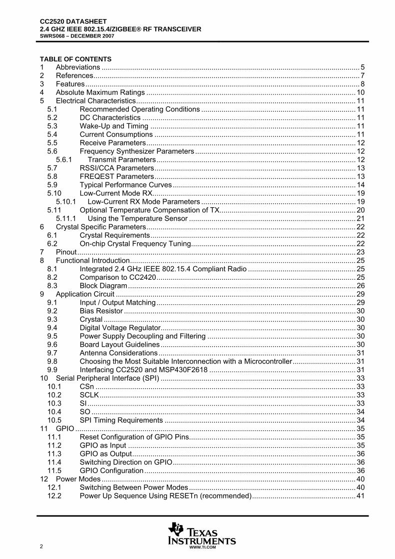
TABLE OF CONTENTS 1 Abbreviations ............................................................................................................................... 5 2 References................................................................................................................................... 7 3 Features....................................................................................................................................... 8 4 Absolute Maximum Ratings .......................................................................................................10 5 Electrical Characteristics............................................................................................................ 11
5.1 Recommended Operating Conditions ............................................................................ 11 5.2 DC Characteristics ......................................................................................................... 11 5.3 Wake-Up and Timing ..................................................................................................... 11 5.4 Current Consumptions ................................................................................................... 11 5.5 Receive Parameters....................................................................................................... 12 5.6 Frequency Synthesizer Parameters ............................................................................... 12
5.6.1 Transmit Parameters.................................................................................................. 12 5.7 RSSI/CCA Parameters................................................................................................... 13 5.8 FREQEST Parameters................................................................................................... 13 5.9 Typical Performance Curves.......................................................................................... 14 5.10 Low-Current Mode RX.................................................................................................... 19
5.10.1 Low-Current RX Mode Parameters ............................................................................ 19 5.11 Optional Temperature Compensation of TX................................................................... 20
5.11.1 Using the Temperature Sensor .................................................................................. 21 6 Crystal Specific Parameters....................................................................................................... 22
6.1 Crystal Requirements..................................................................................................... 22 6.2 On-chip Crystal Frequency Tuning................................................................................. 22
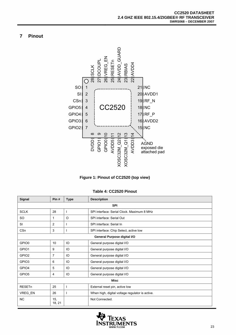
7 Pinout......................................................................................................................................... 23 8 Functional Introduction............................................................................................................... 25
8.1 Integrated 2.4 GHz IEEE 802.15.4 Compliant Radio ..................................................... 25 8.2 Comparison to CC2420.................................................................................................. 25 8.3 Block Diagram................................................................................................................ 26
9 Application Circuit ...................................................................................................................... 29 9.1 Input / Output Matching.................................................................................................. 29 9.2 Bias Resistor ..................................................................................................................30 9.3 Crystal ............................................................................................................................ 30 9.4 Digital Voltage Regulator................................................................................................ 30 9.5 Power Supply Decoupling and Filtering ......................................................................... 30 9.6 Board Layout Guidelines................................................................................................ 30 9.7 Antenna Considerations................................................................................................. 31 9.8 Choosing the Most Suitable Interconnection with a Microcontroller............................... 31 9.9 Interfacing CC2520 and MSP430F2618 ........................................................................ 31
10 Serial Peripheral Interface (SPI) ................................................................................................ 33 10.1 CSn ................................................................................................................................ 33 10.2 SCLK.............................................................................................................................. 33 10.3 SI.................................................................................................................................... 33 10.4 SO .................................................................................................................................. 34 10.5 SPI Timing Requirements .............................................................................................. 34
11 GPIO .......................................................................................................................................... 35 11.1 Reset Configuration of GPIO Pins.................................................................................. 35 11.2 GPIO as Input ................................................................................................................ 35 11.3 GPIO as Output.............................................................................................................. 36 11.4 Switching Direction on GPIO.......................................................................................... 36 11.5 GPIO Configuration........................................................................................................ 36
12 Power Modes ............................................................................................................................. 40 12.1 Switching Between Power Modes.................................................................................. 40 12.2 Power Up Sequence Using RESETn (recommended)................................................... 41
CC2520 DATASHEET2.4 GHZ IEEE 802.15.4/ZIGBEE® RF TRANSCEIVER
SWRS068 – DECEMBER 2007
WWW.TI.COM 3
12.3 Power Up With SRES .................................................................................................... 41 13 Instruction Set ............................................................................................................................ 43
13.1 Definitions ...................................................................................................................... 43 13.2 Instruction Descriptions.................................................................................................. 43 13.3 Instruction Set Summary................................................................................................ 51 13.4 Status Byte..................................................................................................................... 53 13.5 Command Strobes ......................................................................................................... 53 13.6 Command Strobe Buffer ................................................................................................ 53
14 Exceptions ................................................................................................................................. 55 14.1 Exceptions on GPIO Pins............................................................................................... 56 14.2 Predefined Exception Channels..................................................................................... 56 14.3 Binding Exceptions to Instructions (command strobes) ................................................. 57
15 Memory Map .............................................................................................................................. 59 15.1 FREG ............................................................................................................................. 60 15.2 SREG ............................................................................................................................. 60 15.3 TX FIFO ......................................................................................................................... 60 15.4 RX FIFO ......................................................................................................................... 60 15.5 MEM............................................................................................................................... 60 15.6 Frame Filtering and Source Matching Memory Map ...................................................... 60
16 Frequency and Channel Programming ...................................................................................... 62 17 IEEE 802.15.4-2006 Modulation Format.................................................................................... 63 18 IEEE 802.15.4-2006 Frame Format........................................................................................... 65
18.1 PHY Layer ......................................................................................................................65 18.2 MAC Layer ..................................................................................................................... 65
19 Transmit Mode ........................................................................................................................... 67 19.1 TX Control ...................................................................................................................... 67 19.2 TX State Timing ............................................................................................................. 67 19.3 TX FIFO Access............................................................................................................. 67
19.3.1 Retransmission........................................................................................................... 68 19.3.2 Error Conditions ......................................................................................................... 68
19.4 TX Flow Diagram ........................................................................................................... 69 19.5 Frame Processing .......................................................................................................... 70
19.5.1 Synchronization Header ............................................................................................. 70 19.5.2 Frame Length Field .................................................................................................... 70 19.5.3 Frame Check Sequence............................................................................................. 70
19.6 Exceptions...................................................................................................................... 71 19.7 Clear Channel Assessment............................................................................................ 71 19.8 Output Power Programming........................................................................................... 71 19.9 Tips And Tricks .............................................................................................................. 72
20 Receive Mode ............................................................................................................................ 73 20.1 RX Control...................................................................................................................... 73 20.2 RX State Timing ............................................................................................................. 73 20.3 Frame Processing .......................................................................................................... 73
20.3.1 Synchronization Header And Frame Length Fields.................................................... 74 20.3.2 Frame Filtering ........................................................................................................... 74 20.3.3 Source Address Matching .......................................................................................... 77 20.3.4 Frame Check Sequence............................................................................................. 80 20.3.5 Acknowledgement Transmission................................................................................ 81
20.4 RX FIFO Access ............................................................................................................ 82 20.4.1 Using the FIFO and FIFOP Signals............................................................................ 82 20.4.2 Error Conditions ......................................................................................................... 83
20.5 RSSI............................................................................................................................... 83 20.6 Link Quality Indication .................................................................................................... 84
CC2520 DATASHEET 2.4 GHZ IEEE 802.15.4/ZIGBEE® RF TRANSCEIVER SWRS068 – DECEMBER 2007
4 WWW.TI.COM
21 Radio Control State Machine ..................................................................................................... 85 22 Crystal Oscillator........................................................................................................................ 87 23 External Clock Output ................................................................................................................ 88 24 Random Number Generation..................................................................................................... 89 25 Memory Management Instructions............................................................................................. 91
25.1 RXBUFMOV................................................................................................................... 92 25.2 TXBUFCP ...................................................................................................................... 92 25.3 MEMCP..........................................................................................................................92 25.4 MEMCPR ....................................................................................................................... 92 25.5 MEMXCP ....................................................................................................................... 92
26 Security Instructions................................................................................................................... 93 26.1 Decoding of the Flags Field in CC2520.......................................................................... 93 26.2 INC ................................................................................................................................. 94 26.3 ECB................................................................................................................................ 94 26.4 ECBO ............................................................................................................................. 95 26.5 ECBX ............................................................................................................................. 95 26.6 CTR / UCTR................................................................................................................... 96 26.7 CBC-MAC ...................................................................................................................... 97 26.8 CCM / UCCM ................................................................................................................. 97
26.8.1 Inputs to the CCM and UCCM Instructions ................................................................ 97 26.9 Examples from IEEE802.15.4-2006............................................................................... 98
26.9.1 Authentication Only Using CCM* ............................................................................... 99 26.9.2 Encryption Only Using CCM* ..................................................................................... 99 26.9.3 Combination of Encryption and Authentication Using CCM*.................................... 100
27 Packet Sniffing ......................................................................................................................... 101 28 Registers.................................................................................................................................. 102
28.1 Register Settings Update ............................................................................................. 103 28.2 Register Access Modes................................................................................................ 103 28.3 Register Descriptions ................................................................................................... 105
29 Datasheet Revision History...................................................................................................... 126 30 Packaging Information ............................................................................................................. 127
30.1 Mechanical Data .......................................................................................................... 128
CC2520 DATASHEET2.4 GHZ IEEE 802.15.4/ZIGBEE® RF TRANSCEIVER
SWRS068 – DECEMBER 2007
WWW.TI.COM 5
1 Abbreviations AAF Anti Aliasing Filter ACK Acknowledge ADC Analog to Digital Converter ADI Analog-Digital Interface AES Advanced Encryption Standard AGC Automatic Gain Control AM Active Mode ARIB Association of Radio Industries and Businesses BER Bit Error Rate BIST Built In Self Test CBC-MAC Cipher Block Chaining Message Authentication Code CCA Clear Channel Assessment CCM Counter mode + CBC-MAC CDM Charged Device Model CFR Code of Federal Regulations CHP Charge Pump CMOS Complementary Metal Oxide Semiconductor CRC Cyclic Redundancy Check CSMA-CA Carrier Sense Multiple Access with Collision Avoidance CTR Counter mode (encryption) CW Continuous Wave DAC Digital to Analog Converter DC Direct Current DPU Data Processing Unit DSSS Direct Sequence Spread Spectrum ECB Electronic Code Book (mode of AES operation) ESD Electro Static Discharge ESR Equivalent Series Resistance ETSI European Telecommunications Standards Institute EU European Union EVM Error Vector Magnitude FCC Federal Communications Commission FCF Frame Control Field FCS Frame Check Sequence FFCTRL FIFO and Frame Control FIFO First In First Out FS Frequency Synthesizer FSM Finite State Machine GPIO General Purpose Input/Output HBM Human Body Model HSSD High Speed Serial Debug I/O Input / Output I/Q In-phase / Quadrature-phase IEEE Institute of Electrical and Electronics Engineers IF Intermediate Frequency ISM Industrial, Scientific and Medical ITU-T International Telecommunication Union –
Telecommunication Standardization Sector kbps kilo bits per second LB Loop Back LF Loop Filter LNA Low-Noise Amplifier LO Local Oscillator LPF Low Pass Filter LPM Low-Power Mode
CC2520 DATASHEET 2.4 GHZ IEEE 802.15.4/ZIGBEE® RF TRANSCEIVER SWRS068 – DECEMBER 2007
6 WWW.TI.COM
LQI Link Quality Indication LSB Least Significant Bit / Byte LUT Look-Up Table MAC Medium Access Control MCU Micro Controller Unit MFR MAC Footer MHR MAC Header MIC Message Integrity Code MISO Master In Slave Out MM Machine Model MOSI Master Out Slave In MPDU MAC Protocol Data Unit MSB Most significant Bit / Byte MSDU MAC Service Data Unit NA Not Available NC Not Connected O-QPSK Offset - Quadrature Phase Shift Keying PA Power Amplifier PAN Personal Area Network PCB Printed Circuit Board PD Power Down, Phase Detector PER Packet Error Rate PHR PHY Header PHY Physical Layer PLL Phase Locked Loop PQFP Plastic Quad FlatPack PSDU PHY Service Data Unit PUE Pull-Up Enable QLP Quad Leadless Package RAM Random Access Memory RBW Resolution BandWidth RF Radio Frequency RHD Not actually an acronym. This is the package name used in TI. RISC Reduced Instruction Set Computer RoHS Restriction of Hazardous Substances Directive ROM Read Only Memory RSSI Received Signal Strength Indicator RX Receive SFD Start of Frame Delimiter SHR Synchronization Header SI Serial In SO Serial Out SPI Serial Peripheral Interface S-PQFP Plastic Quad Flat Pack T/R Transmit / Receive TBD To Be Decided / To Be Defined TX Transmit UI User Interface VCO Voltage Controlled Oscillator VGA Variable Gain Amplifier XOSC Crystal Oscillator LR Low Rate NaN Not any Number
CC2520 DATASHEET2.4 GHZ IEEE 802.15.4/ZIGBEE® RF TRANSCEIVER
SWRS068 – DECEMBER 2007
WWW.TI.COM 7
2 References [1] IEEE std. 802.15.4 - 2003: Wireless Medium Access Control (MAC) and Physical Layer (PHY)
specifications for Low Rate Wireless Personal Area Networks (LR-WPANs) http://standards.ieee.org/getieee802/download/802.15.4-2003.pdf
[2] IEEE std. 802.15.4 - 2006: Wireless Medium Access Control (MAC) and Physical Layer (PHY) specifications for Low Rate Wireless Personal Area Networks (LR-WPANs) http://standards.ieee.org/getieee802/download/802.15.4-2006.pdf
[3] CC2420 datasheet http://www.ti.com/lit/pdf/swrs041
[4] NIST FIPS Pub 197: Advanced Encryption Standard (AES), Federal Information Processing Standards Publication 197, US Department of Commerce/N.I.S.T., November 26, 2001. http://csrc.nist.gov/publications/fips/fips197/fips-197.pdf
[5] CC2520 reference designs http://focus.ti.com/docs/prod/folders/print/cc2520.html#applicationnotes
[6] CC2520 Errata note http://www.ti.com/lit/pdf/swrz024
[7] CC2520 Product folder http://focus.ti.com/docs/prod/folders/print/cc2520.html
[8] NIST software package for randomness testing: http://csrc.nist.gov/rng/
[9] The diehard software package for randomness testing: http://stat.fsu.edu/~geo/diehard.html
[10] MSP430F2618 Product folder http://focus.ti.com/docs/prod/folders/print/msp430f2618.html
[11] 2.4 GHz Inverted F Antenna http://www.ti.com/lit/pdf/swru120
[12] Antenna selection guide http://www.ti.com/lit/pdf/swra161
CC2520 DATASHEET 2.4 GHZ IEEE 802.15.4/ZIGBEE® RF TRANSCEIVER SWRS068 – DECEMBER 2007
8 WWW.TI.COM
3 Features 2394-2507MHz transceiver • DSSS transceiver • 250kbps data rate, 2 MChip/s chip rate • O-QPSK with half sine pulse shaping modulation • Very low current consumption
RX (receiving frame, -50 dBm): 18.5 mA RX (waiting for frame): 22.3 mA TX (+5 dBm output power): 33.6 mA TX (0 dBm output power): 25.8 mA
• Three flexible power modes for reduced power consumption • Low power fully static CMOS design • Very good sensitivity (-98dBm) • High adjacent channel rejection (49 dB) • High alternate channel rejection (54 dB) • On chip VCO, LNA, PA and filters. • Low supply voltage (1.8 - 3.8 V) • Programmable output power up to +5 dBm • I/Q direct conversion transceiver Small Size • QFN 28 (RHD) package, 5 x 5 mm • Very few external components
o minimized number of passives o Only reference crystal needed
• Clock output for other ICs to limit the number of crystals needed in a system • No external filters needed. Easy and Flexible User Interface • 4-wire SPI • Serial clock up to 8 MHz • 6 GPIO pins with full flexibility • Interrupt generator • Full control of automatic responses to different events • Embedded packet sniffer mode • CC2420 compatibility mode Data Processing Unit For Advanced Data Handling • Spacious (768 byte) on-chip RAM allows powerful on-chip frame processing • 128 byte transmit data FIFO • 128 byte receive data FIFO • Full read and write access to RAM • 128 bit AES IEEE 802.15.4 MAC Hardware Support • Automatic preamble generator • Synchronization word insertion and detection • CRC-16 computation and verification over the MAC payload • Frame filtering • Automatic ACK and setting of the pending-bit • Clear Channel Assessment (CCA) • Energy detection / RSSI • Link Quality Indication (LQI) • Fully automatic MAC security (CTR, CBC-MAC, CCM)
CC2520 DATASHEET2.4 GHZ IEEE 802.15.4/ZIGBEE® RF TRANSCEIVER
SWRS068 – DECEMBER 2007
WWW.TI.COM 9
Development Tools • See product folder [7] Suited For Use in Systems That Target Compliance to the Following Standards • IEEE 802.15.4 PHY • ETSI EN 300 328 • ETSI EN 300 440 class 2 • FCC CFR47 part 15 • ARIB STD-T66
CC2520 DATASHEET 2.4 GHZ IEEE 802.15.4/ZIGBEE® RF TRANSCEIVER SWRS068 – DECEMBER 2007
10 WWW.TI.COM
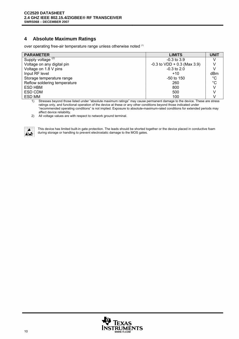
4 Absolute Maximum Ratings over operating free-air temperature range unless otherwise noted (1) PARAMETER LIMITS UNIT Supply voltage (2) -0.3 to 3.9 V Voltage on any digital pin -0.3 to VDD + 0.3 (Max 3.9) V Voltage on 1.8 V pins -0.3 to 2.0 V Input RF level +10 dBm Storage temperature range -50 to 150 °C Reflow soldering temperature 260 °C ESD HBM 800 V ESD CDM 500 V ESD MM 100 V
1) Stresses beyond those listed under “absolute maximum ratings” may cause permanent damage to the device. These are stress ratings only, and functional operation of the device at these or any other conditions beyond those indicated under “recommended operating conditions” is not implied. Exposure to absolute-maximum-rated conditions for extended periods may affect device reliability.
2) All voltage values are with respect to network ground terminal.
This device has limited built-in gate protection. The leads should be shorted together or the device placed in conductive foam during storage or handling to prevent electrostatic damage to the MOS gates.
CC2520 DATASHEET2.4 GHZ IEEE 802.15.4/ZIGBEE® RF TRANSCEIVER
SWRS068 – DECEMBER 2007
WWW.TI.COM 11
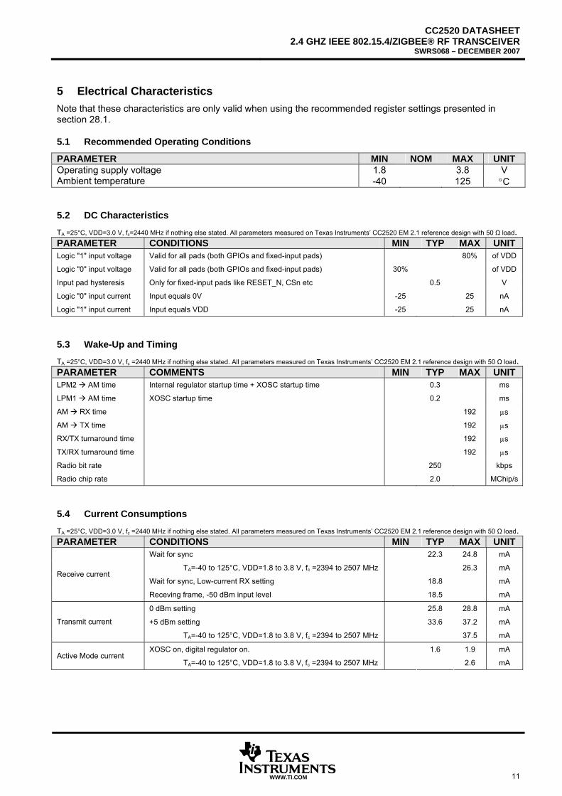
5 Electrical Characteristics Note that these characteristics are only valid when using the recommended register settings presented in section 28.1.
5.1 Recommended Operating Conditions
PARAMETER MIN NOM MAX UNIT Operating supply voltage 1.8 3.8 V Ambient temperature -40 125 °C
5.2 DC Characteristics
TA =25°C, VDD=3.0 V, fc=2440 MHz if nothing else stated. All parameters measured on Texas Instruments’ CC2520 EM 2.1 reference design with 50 Ω load. PARAMETER CONDITIONS MIN TYP MAX UNIT Logic "1" input voltage Valid for all pads (both GPIOs and fixed-input pads) 80% of VDD
Logic "0" input voltage Valid for all pads (both GPIOs and fixed-input pads) 30% of VDD
Input pad hysteresis Only for fixed-input pads like RESET_N, CSn etc 0.5 V
Logic "0" input current Input equals 0V -25 25 nA
Logic "1" input current Input equals VDD -25 25 nA
5.3 Wake-Up and Timing
TA =25°C, VDD=3.0 V, fc =2440 MHz if nothing else stated. All parameters measured on Texas Instruments’ CC2520 EM 2.1 reference design with 50 Ω load. PARAMETER COMMENTS MIN TYP MAX UNIT LPM2 AM time Internal regulator startup time + XOSC startup time 0.3 ms
LPM1 AM time XOSC startup time 0.2 ms
AM RX time 192 µs
AM TX time 192 µs
RX/TX turnaround time 192 µs
TX/RX turnaround time 192 µs
Radio bit rate 250 kbps
Radio chip rate 2.0 MChip/s
5.4 Current Consumptions
TA =25°C, VDD=3.0 V, fc =2440 MHz if nothing else stated. All parameters measured on Texas Instruments’ CC2520 EM 2.1 reference design with 50 Ω load. PARAMETER CONDITIONS MIN TYP MAX UNIT
Wait for sync 22.3 24.8 mA
TA=-40 to 125°C, VDD=1.8 to 3.8 V, fc =2394 to 2507 MHz 26.3 mA
Wait for sync, Low-current RX setting 18.8 mA Receive current
Receving frame, -50 dBm input level 18.5 mA
0 dBm setting 25.8 28.8 mA
+5 dBm setting 33.6 37.2 mA Transmit current
TA=-40 to 125°C, VDD=1.8 to 3.8 V, fc =2394 to 2507 MHz 37.5 mA
XOSC on, digital regulator on. 1.6 1.9 mA Active Mode current
TA=-40 to 125°C, VDD=1.8 to 3.8 V, fc =2394 to 2507 MHz 2.6 mA
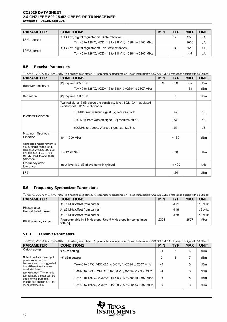
CC2520 DATASHEET 2.4 GHZ IEEE 802.15.4/ZIGBEE® RF TRANSCEIVER SWRS068 – DECEMBER 2007
12 WWW.TI.COM
PARAMETER CONDITIONS MIN TYP MAX UNIT XOSC off, digital regulator on. State retention. 175 250 µA
LPM1 current TA=-40 to 125°C, VDD=1.8 to 3.8 V, fc =2394 to 2507 MHz 1000 µA
XOSC off, digital regulator off. No state retention. 30 120 nA LPM2 current
TA=-40 to 125°C, VDD=1.8 to 3.8 V, fc =2394 to 2507 MHz 4.5 µA
5.5 Receive Parameters
TA =25°C, VDD=3.0 V, fc =2440 MHz if nothing else stated. All parameters measured on Texas Instruments’ CC2520 EM 2.1 reference design with 50 Ω load. PARAMETER CONDITIONS MIN TYP MAX UNIT
[2] requires -85 dBm -99 -98 -95 dBm Receiver sensitivity
TA=-40 to 125°C, VDD=1.8 to 3.8V, fc =2394 to 2507 MHz -88 dBm
Saturation [2] requires -20 dBm 6 dBm
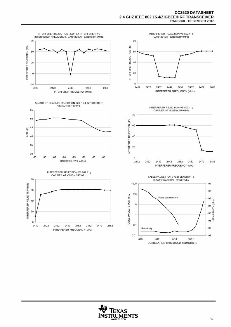
Wanted signal 3 dB above the sensitivity level, 802.15.4 modulated interferer at 802.15.4 channels:
±5 MHz from wanted signal. [2] requires 0 dB 49 dB
±10 MHz from wanted signal. [2] requires 30 dB 54 dB Interferer Rejection
±20MHz or above. Wanted signal at -82dBm. 55 dB
30 – 1000 MHz < -80 dBm Maximum Spurious Emission Conducted measurement in a 50Ω single ended load. Complies with EN 300 328, EN 300 440 class 2, FCC CFR47, Part 15 and ARIB STD-T-66
1 – 12.75 GHz -56 dBm
Frequency error tolerance Input level is 3 dB above sensitivity level. +/-400 kHz
IIP3 -24 dBm
5.6 Frequency Synthesizer Parameters
TA =25°C, VDD=3.0 V, fc =2440 MHz if nothing else stated. All parameters measured on Texas Instruments’ CC2520 EM 2.1 reference design with 50 Ω load. PARAMETER CONDITIONS MIN TYP MAX UNIT
At ±1 MHz offset from carrier -111 dBc/Hz
At ±2 MHz offset from carrier -118 dBc/Hz Phase noise. Unmodulated carrier
At ±5 MHz offset from carrier -128 dBc/Hz
RF Frequency range Programmable in 1 MHz steps. Use 5 MHz steps for compliance with [2].
2394 2507 MHz
5.6.1 Transmit Parameters
TA =25°C, VDD=3.0 V, fc =2440 MHz if nothing else stated. All parameters measured on Texas Instruments’ CC2520 EM 2.1 reference design with 50 Ω load. PARAMETER CONDITIONS MIN TYP MAX UNIT
0 dBm setting -3 1 5 dBm
+5 dBm setting 2 5 7 dBm
TA=-40 to 85°C, VDD=2.0 to 3.8 V, fc =2394 to 2507 MHz -3 8 dBm
TA=-40 to 85°C , VDD=1.8 to 3.8 V, fc =2394 to 2507 MHz -4 8 dBm
TA=-40 to 125°C, VDD=2.0 to 3.8 V, fc =2394 to 2507 MHz -6 8 dBm
Output power Note: to reduce the output power variation over temperature, it is suggested that different settings are used at different temperatures. The on-chip temperature sensor can be used for this purpose. Please see section 5.11 for more information. TA=-40 to 125°C, VDD=1.8 to 3.8 V, fc =2394 to 2507 MHz -9 8 dBm
CC2520 DATASHEET2.4 GHZ IEEE 802.15.4/ZIGBEE® RF TRANSCEIVER
SWRS068 – DECEMBER 2007
WWW.TI.COM 13
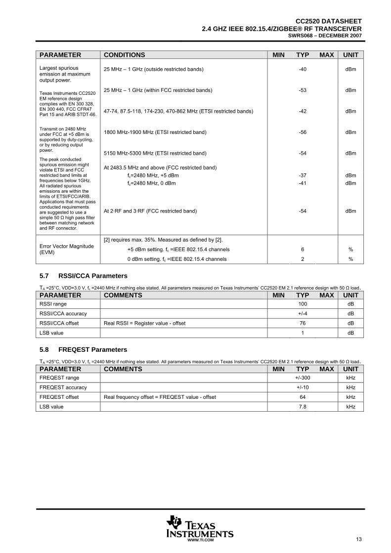
PARAMETER CONDITIONS MIN TYP MAX UNIT
25 MHz – 1 GHz (outside restricted bands) -40 dBm
25 MHz – 1 GHz (within FCC restricted bands) -53 dBm
47-74, 87.5-118, 174-230, 470-862 MHz (ETSI restricted bands) -42 dBm
1800 MHz-1900 MHz (ETSI restricted band) -56 dBm
5150 MHz-5300 MHz (ETSI restricted band) -54 dBm
At 2483.5 MHz and above (FCC restricted band) fc=2480 MHz, +5 dBm -37 dBm fc=2480 MHz, 0 dBm -41 dBm
Largest spurious emission at maximum output power. Texas Instruments CC2520 EM reference design complies with EN 300 328, EN 300 440, FCC CFR47 Part 15 and ARIB STDT-66.
Transmit on 2480 MHz under FCC at +5 dBm is supported by duty-cycling, or by reducing output power.
The peak conducted spurious emission might violate ETSI and FCC restricted band limits at frequencies below 1GHz. All radiated spurious emissions are within the limits of ETSI/FCC/ARIB. Applications that must pass conducted requirements are suggested to use a simple 50 Ω high pass filter between matching network and RF connector.
At 2·RF and 3·RF (FCC restricted band) -54 dBm
[2] requires max. 35%. Measured as defined by [2].
+5 dBm setting. fc =IEEE 802.15.4 channels 6 % Error Vector Magnitude (EVM)
0 dBm setting. fc =IEEE 802.15.4 channels 2 %
5.7 RSSI/CCA Parameters
TA =25°C, VDD=3.0 V, fc =2440 MHz if nothing else stated. All parameters measured on Texas Instruments’ CC2520 EM 2.1 reference design with 50 Ω load. PARAMETER COMMENTS MIN TYP MAX UNIT RSSI range 100 dB
RSSI/CCA accuracy +/-4 dB
RSSI/CCA offset Real RSSI = Register value - offset 76 dB
LSB value 1 dB
5.8 FREQEST Parameters
TA =25°C, VDD=3.0 V, fc =2440 MHz if nothing else stated. All parameters measured on Texas Instruments’ CC2520 EM 2.1 reference design with 50 Ω load. PARAMETER COMMENTS MIN TYP MAX UNIT FREQEST range +/-300 kHz
FREQEST accuracy +/-10 kHz
FREQEST offset Real frequency offset = FREQEST value - offset 64 kHz
LSB value 7.8 kHz
CC2520 DATASHEET 2.4 GHZ IEEE 802.15.4/ZIGBEE® RF TRANSCEIVER SWRS068 – DECEMBER 2007
14 WWW.TI.COM
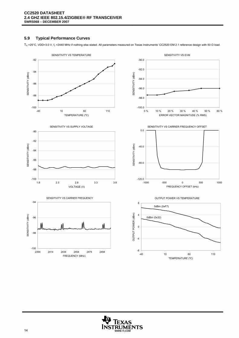
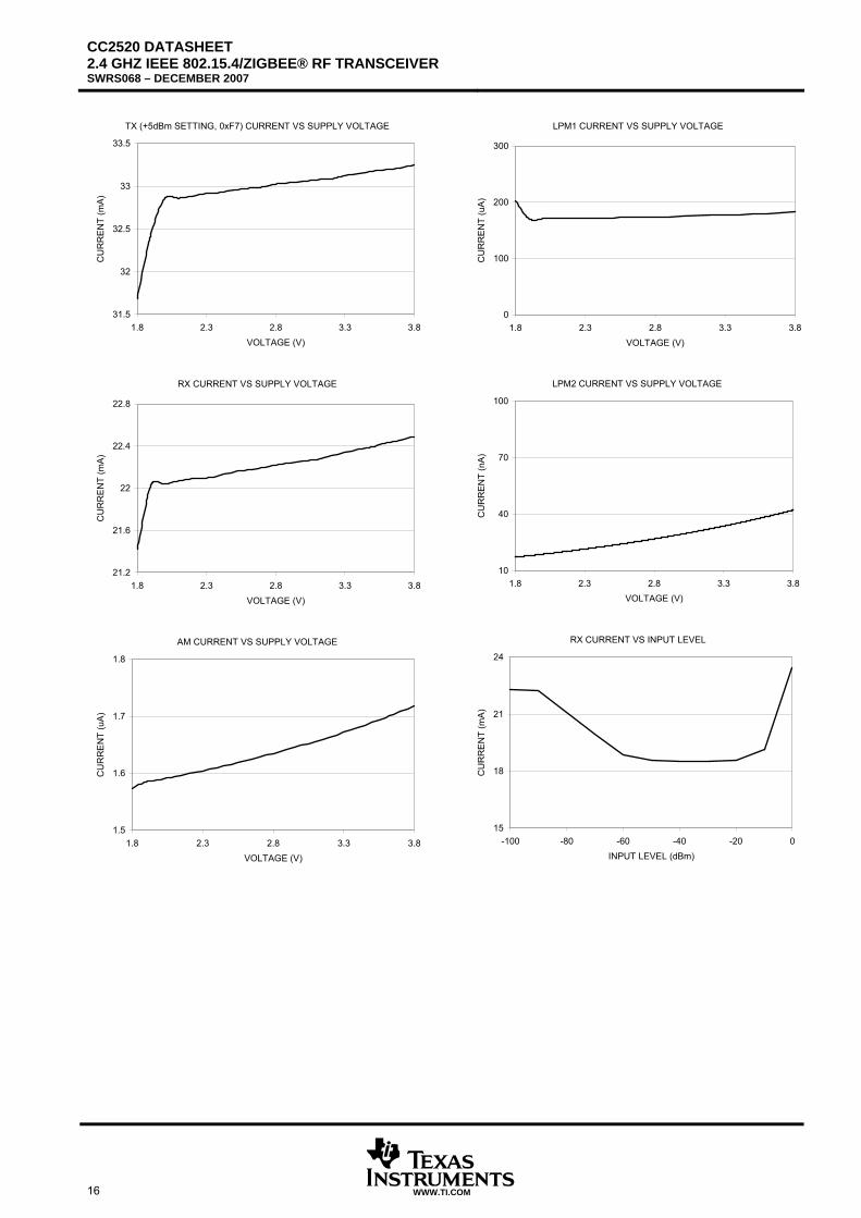
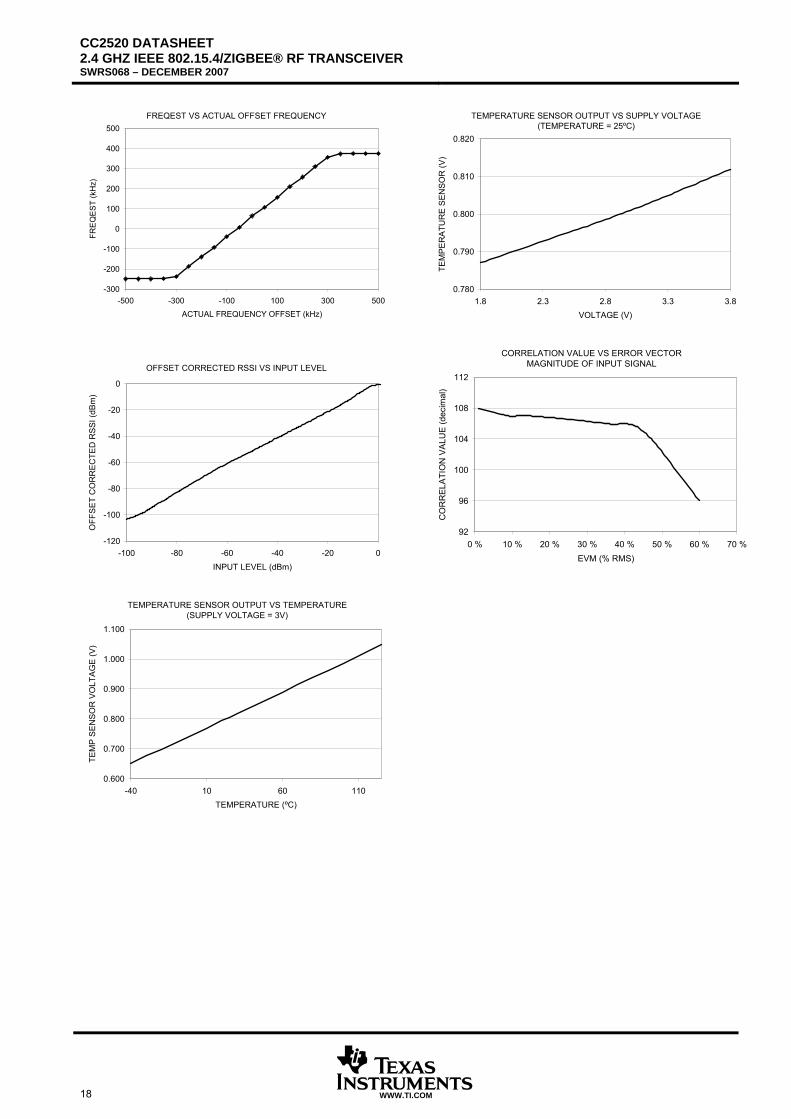
5.9 Typical Performance Curves TA =25°C, VDD=3.0 V, fc =2440 MHz if nothing else stated. All parameters measured on Texas Instruments’ CC2520 EM 2.1 reference design with 50 Ω load.
SENSITIVITY VS TEMPERATURE
-100
-98
-96
-94
-92
-40 10 60 110TEMPERATURE (ºC)
SEN
SIT
IVIT
Y (d
Bm
)
SENSITIVITY VS SUPPLY VOLTAGE
-100
-98
-96
-94
-92
-90
1.8 2.3 2.8 3.3 3.8VOLTAGE (V)
SE
NS
ITIV
ITY
(dB
m)
SENSITIVITY VS CARRIER FREQUENCY
-100
-98
-96
-94
2394 2414 2434 2454 2474 2494FREQUENCY (MHz)
SEN
SIT
IVIT
Y (d
Bm)
SENSITIVITY VS EVM
-100.0
-98.0
-96.0
-94.0
-92.0
-90.0
0 % 10 % 20 % 30 % 40 % 50 % 60 %ERROR VECTOR MAGNITUDE (% RMS)
SEN
SIT
IVIT
Y (d
Bm
)
SENSITIVITY VS CARRIER FREQUENCY OFFSET
-120.0
-80.0
-40.0
0.0
-1000 -500 0 500 1000FREQUENCY OFFSET (kHz)
SEN
SITI
VITY
(dBm
)
OUTPUT POWER VS TEMPERATURE
-8
-4
0
4
8
-40 10 60 110TEMPERATURE (ºC)
OU
TPU
T P
OW
ER (d
Bm
)
5dBm (0xF7)
0dBm (0x32)
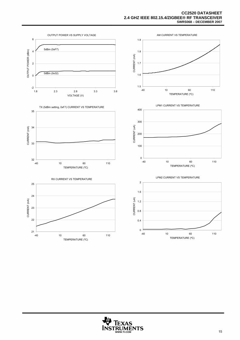
CC2520 DATASHEET2.4 GHZ IEEE 802.15.4/ZIGBEE® RF TRANSCEIVER
SWRS068 – DECEMBER 2007
WWW.TI.COM 15
OUTPUT POWER VS SUPPLY VOLTAGE
-2
0
2
4
6
1.8 2.3 2.8 3.3 3.8VOLTAGE (V)
OU
TPU
T P
OW
ER
(dBm
) 5dBm (0xF7)
0dBm (0x32)
TX (5dBm setting, 0xF7) CURRENT VS TEMPERATURE
32
33
34
35
-40 10 60 110TEMPERATURE (ºC)
CU
RR
EN
T (m
A)
RX CURRENT VS TEMPERATURE
21
22
23
24
25
-40 10 60 110TEMPERATURE (ºC)
CU
RR
EN
T (m
A)
AM CURRENT VS TEMPERATURE
1.5
1.6
1.7
1.8
1.9
-40 10 60 110TEMPERATURE (ºC)
CU
RR
ENT
(mA
)
LPM1 CURRENT VS TEMPERATURE
0
100
200
300
400
-40 10 60 110TEMPERATURE (ºC)
CU
RR
EN
T (u
A)
LPM2 CURRENT VS TEMPERATURE
0
0.4
0.8
1.2
1.6
2
-40 10 60 110TEMPERATURE (ºC)
CU
RR
EN
T (u
A)
CC2520 DATASHEET 2.4 GHZ IEEE 802.15.4/ZIGBEE® RF TRANSCEIVER SWRS068 – DECEMBER 2007
16 WWW.TI.COM
TX (+5dBm SETTING, 0xF7) CURRENT VS SUPPLY VOLTAGE
31.5
32
32.5
33
33.5
1.8 2.3 2.8 3.3 3.8VOLTAGE (V)
CU
RR
EN
T (m
A)
RX CURRENT VS SUPPLY VOLTAGE
21.2
21.6
22
22.4
22.8
1.8 2.3 2.8 3.3 3.8VOLTAGE (V)
CU
RR
EN
T (m
A)
AM CURRENT VS SUPPLY VOLTAGE
1.5
1.6
1.7
1.8
1.8 2.3 2.8 3.3 3.8VOLTAGE (V)
CU
RR
EN
T (u
A)
LPM1 CURRENT VS SUPPLY VOLTAGE
0
100
200
300
1.8 2.3 2.8 3.3 3.8VOLTAGE (V)
CU
RR
EN
T (u
A)
LPM2 CURRENT VS SUPPLY VOLTAGE
10
40
70
100
1.8 2.3 2.8 3.3 3.8VOLTAGE (V)
CU
RR
ENT
(nA
)
RX CURRENT VS INPUT LEVEL
15
18
21
24
-100 -80 -60 -40 -20 0INPUT LEVEL (dBm)
CU
RR
EN
T (m
A)
CC2520 DATASHEET2.4 GHZ IEEE 802.15.4/ZIGBEE® RF TRANSCEIVER
SWRS068 – DECEMBER 2007
WWW.TI.COM 17
INTERFERER REJECTION (802.15.4 INTERFERER) VS INTERFERER FREQUENCY. CARRIER AT -82dBm/2440MHz.
-25
0
25
50
75
2400 2420 2440 2460 2480INTERFERER FREQUENCY (MHz)
INTE
RFE
RE
R R
EJE
CTI
ON
(dB
)
ADJACENT CHANNEL REJECTION (802.15.4 INTERFERER) VS CARRIER LEVEL
30
35
40
45
50
55
-95 -90 -85 -80 -75 -70 -65 -60CARRIER LEVEL (dBm)
AC
R (d
B)
INTERFERER REJECTION VS 802.11g CARRIER AT -82dBm/2405MHz
0
20
40
60
80
2412 2422 2432 2442 2452 2462 2472 2482INTERFERER FREQUENCY (MHz)
INTE
RFE
RE
R R
EJE
CTI
ON
(dB
)
INTERFERER REJECTION VS 802.11g CARRIER AT -82dBm/2440MHz
0
20
40
60
80
2412 2422 2432 2442 2452 2462 2472 2482INTERFERER FREQUENCY (MHz)
INTE
RFE
RE
R R
EJE
CTI
ON
(dB
)
INTERFERER REJECTION VS 802.11g
CARRIER AT -82dBm/2480MHz
0
20
40
60
80
2412 2422 2432 2442 2452 2462 2472 2482INTERFERER FREQUENCY (MHz)
INTE
RFE
RE
R R
EJE
CTI
ON
(dB
)
FALSE PACKET RATE AND SENSITIVITY vs CORRELATION THRESHOLD
0.01
0.1
1
10
100
1000
0x0B 0x0F 0x13 0x17CORRELATION THRESHOLD (MDMCTRL1)
FALS
E P
AC
KE
TS P
ER
MIN
.
-98
-97
-96
-95
-94
-93
-92
-91
SE
NS
ITIV
ITY
(dB
m)False packets/min
Sensitivity
CC2520 DATASHEET 2.4 GHZ IEEE 802.15.4/ZIGBEE® RF TRANSCEIVER SWRS068 – DECEMBER 2007
18 WWW.TI.COM
FREQEST VS ACTUAL OFFSET FREQUENCY
-300
-200
-100
0
100
200
300
400
500
-500 -300 -100 100 300 500ACTUAL FREQUENCY OFFSET (kHz)
FRE
QE
ST (k
Hz)
OFFSET CORRECTED RSSI VS INPUT LEVEL
-120
-100
-80
-60
-40
-20
0
-100 -80 -60 -40 -20 0INPUT LEVEL (dBm)
OFF
SE
T C
OR
RE
CTE
D R
SS
I (dB
m)
TEMPERATURE SENSOR OUTPUT VS TEMPERATURE (SUPPLY VOLTAGE = 3V)
0.600
0.700
0.800
0.900
1.000
1.100
-40 10 60 110TEMPERATURE (ºC)
TEM
P SE
NSO
R V
OLT
AG
E (V
)
TEMPERATURE SENSOR OUTPUT VS SUPPLY VOLTAGE (TEMPERATURE = 25ºC)
0.780
0.790
0.800
0.810
0.820
1.8 2.3 2.8 3.3 3.8VOLTAGE (V)
TEM
PER
ATU
RE
SEN
SOR
(V)
CORRELATION VALUE VS ERROR VECTOR MAGNITUDE OF INPUT SIGNAL
92
96
100
104
108
112
0 % 10 % 20 % 30 % 40 % 50 % 60 % 70 %EVM (% RMS)
CO
RR
ELA
TIO
N V
ALU
E (d
ecim
al)
CC2520 DATASHEET2.4 GHZ IEEE 802.15.4/ZIGBEE® RF TRANSCEIVER
SWRS068 – DECEMBER 2007
WWW.TI.COM 19
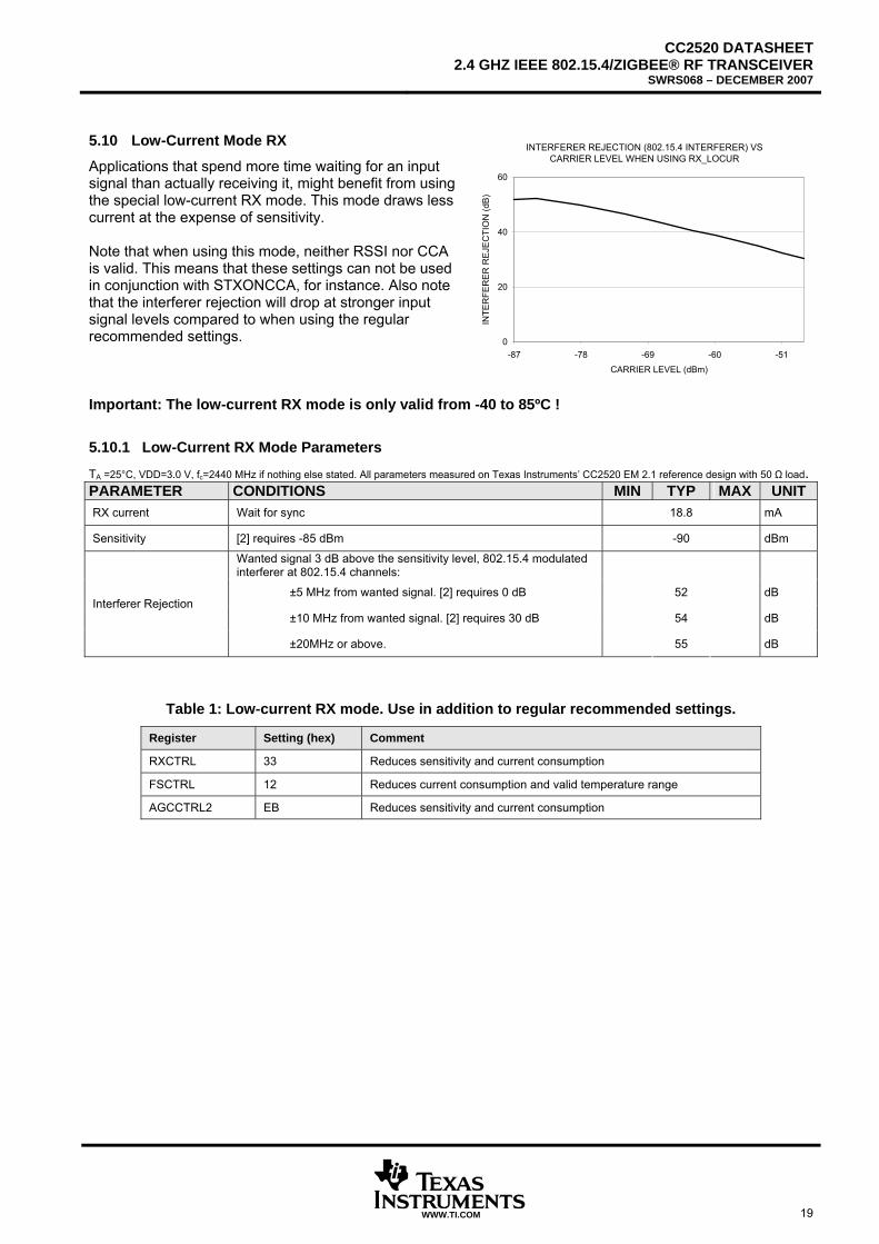
5.10 Low-Current Mode RX
Applications that spend more time waiting for an input signal than actually receiving it, might benefit from using the special low-current RX mode. This mode draws less current at the expense of sensitivity. Note that when using this mode, neither RSSI nor CCA is valid. This means that these settings can not be used in conjunction with STXONCCA, for instance. Also note that the interferer rejection will drop at stronger input signal levels compared to when using the regular recommended settings. Important: The low-current RX mode is only valid from -40 to 85ºC !
5.10.1 Low-Current RX Mode Parameters
TA =25°C, VDD=3.0 V, fc=2440 MHz if nothing else stated. All parameters measured on Texas Instruments’ CC2520 EM 2.1 reference design with 50 Ω load. PARAMETER CONDITIONS MIN TYP MAX UNIT RX current Wait for sync 18.8 mA
Sensitivity [2] requires -85 dBm -90 dBm
Wanted signal 3 dB above the sensitivity level, 802.15.4 modulated interferer at 802.15.4 channels:
±5 MHz from wanted signal. [2] requires 0 dB 52 dB
±10 MHz from wanted signal. [2] requires 30 dB 54 dB Interferer Rejection
±20MHz or above. 55 dB
Table 1: Low-current RX mode. Use in addition to regular recommended settings.
Register Setting (hex) Comment
RXCTRL 33 Reduces sensitivity and current consumption
FSCTRL 12 Reduces current consumption and valid temperature range
AGCCTRL2 EB Reduces sensitivity and current consumption
INTERFERER REJECTION (802.15.4 INTERFERER) VS CARRIER LEVEL WHEN USING RX_LOCUR
0
20
40
60
-87 -78 -69 -60 -51CARRIER LEVEL (dBm)
INTE
RFE
RER
REJ
EC
TIO
N (d
B)
CC2520 DATASHEET 2.4 GHZ IEEE 802.15.4/ZIGBEE® RF TRANSCEIVER SWRS068 – DECEMBER 2007
20 WWW.TI.COM
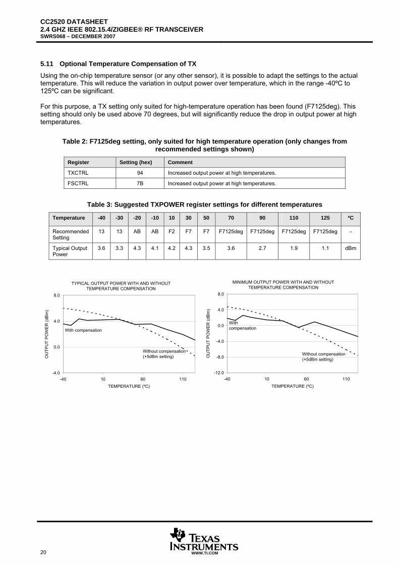
5.11 Optional Temperature Compensation of TX
Using the on-chip temperature sensor (or any other sensor), it is possible to adapt the settings to the actual temperature. This will reduce the variation in output power over temperature, which in the range -40ºC to 125ºC can be significant. For this purpose, a TX setting only suited for high-temperature operation has been found (F7125deg). This setting should only be used above 70 degrees, but will significantly reduce the drop in output power at high temperatures.
Table 2: F7125deg setting, only suited for high temperature operation (only changes from recommended settings shown)
Register Setting (hex) Comment
TXCTRL 94 Increased output power at high temperatures.
FSCTRL 7B Increased output power at high temperatures.
Table 3: Suggested TXPOWER register settings for different temperatures
Temperature -40 -30 -20 -10 10 30 50 70 90 110 125 ºC
Recommended Setting
13 13 AB AB F2 F7 F7 F7125deg F7125deg F7125deg F7125deg -
Typical Output Power
3.6 3.3 4.3 4.1 4.2 4.3 3.5 3.6 2.7 1.9 1.1 dBm
TYPICAL OUTPUT POWER WITH AND WITHOUT TEMPERATURE COMPENSATION
-4.0
0.0
4.0
8.0
-40 10 60 110TEMPERATURE (ºC)
OU
TPU
T PO
WE
R (d
Bm
)
With compensation
Without compensation(+5dBm setting)
MINIMUM OUTPUT POWER WITH AND WITHOUT TEMPERATURE COMPENSATION
-12.0
-8.0
-4.0
0.0
4.0
8.0
-40 10 60 110TEMPERATURE (ºC)
OU
TPU
T P
OW
ER (d
Bm)
With compensation
Without compensation(+5dBm setting)
CC2520 DATASHEET2.4 GHZ IEEE 802.15.4/ZIGBEE® RF TRANSCEIVER
SWRS068 – DECEMBER 2007
WWW.TI.COM 21
5.11.1 Using the Temperature Sensor
The on-chip temperature sensor can be accessed via the GPIO0 and GPIO1 pins by following this procedure: • Configure GPIO0 and GPIO1 as inputs by writing 0x80 to the GPIOCTRL0 and GPIOCTRL1 registers. • Enable analog output functionality for these two pins by setting GPIOCTRL.GPIO_ACTRL=’1’. • Select temperature sensor output by writing 0x01 to the ATEST register. This will make GPIO1 output
GND and GPIO0 will output a voltage proportional to the temperature. • Use an ADC in the microcontroller to measure the output voltage on GPIO0 and then calculate the
temperature. The output from the temperature sensor is shown in graph form in section 5.9, but as a basis for calculating the temperature, the following numbers can be used: Tc=-40 – 125°C, VDD=1.8 – 3.8 V
Parameter Min Typ Max Unit
Temp sensor voltage at 25°C 0.8 V
Temp. sens. output vs temperature 25 mV/10°C
Temp. sens. output vs supply voltage 6 mV/V
Temp. sens accuracy no calibration (at fixed voltage) +/-12 °C
Temp, sens. accuracy with 1-point calibration (at fixed voltage) +/-1 °C
CC2520 DATASHEET 2.4 GHZ IEEE 802.15.4/ZIGBEE® RF TRANSCEIVER SWRS068 – DECEMBER 2007
22 WWW.TI.COM
6 Crystal Specific Parameters
6.1 Crystal Requirements
PARAMETER CONDITIONS MIN TYP MAX UNIT
Crystal frequency 32 MHz
Crystal frequency accuracy requirement
Including initial tolerance, aging and temperature dependency, as specified by [2]. Can be relaxed using on-chip crystal tuning (see below).
- 40
40 ppm
ESR 60 Ohm
C0 7 pF
CL 16 pF
6.2 On-chip Crystal Frequency Tuning
PARAMETER CONDITIONS MIN TYP MAX UNIT
Crystal tuning range (Ctune) Only adding capacitance is possible 7 pF Crystal tuning step size 0.4 pF Crystal tuning drift In % of applied tuning +/-10 %
CRYSTAL TUNING USING CC2520 EM 2.1 REFERENCE DESIGN (NX3225DA, CL = 16 pF) :
Start-up time 0.2 ms Crystal tuning step size 3 ppm Crystal tuning range
NDK crystal NX3225DA, CL=16 pF
-45 ppm CRYSTAL TUNING USING OTHER CRYSTALS, ALL NUMBERS ARE ESTIMATES :
Start-up time 0.2 ms
Crystal tuning step size 8 ppm
Crystal tuning range
NDK crystal NX4025DA, CL=13 pF
-120 ppm
Start-up time 0.1 ms
Crystal tuning step size 10 ppm
Crystal tuning range
NDK crystal NX5032SA, CL=10 pF
-160 ppm
See section 22 for further details on using the crystal oscillator.
CC2520 DATASHEET2.4 GHZ IEEE 802.15.4/ZIGBEE® RF TRANSCEIVER
SWRS068 – DECEMBER 2007
WWW.TI.COM 23
7 Pinout
1234567
8 9 10 11 12 13 1415161718192021
28 27 26 25 24 23 22
SOSI
CSnGPIO5GPIO4GPIO3GPIO2
DV
DD
GP
IO1
GP
IO0
AV
DD
5X
OS
C32
M_Q
2X
OS
C32
M_Q
1A
VD
D3
CC2520
NCAVDD2RF_PNCRF_NAVDD1NC
AGNDexposed dieattached pad
SC
LKD
CO
UP
LV
RE
G_E
NR
ES
ETn
AV
DD
_GU
AR
DR
BIA
SA
VD
D4
Figure 1: Pinout of CC2520 (top view)
Table 4: CC2520 Pinout
Signal Pin # Type Description
SPI
SCLK 28 I SPI interface: Serial Clock. Maximum 8 MHz
SO 1 O SPI interface: Serial Out
SI 2 I SPI interface: Serial In
CSn 3 I SPI interface: Chip Select, active low
General Purpose digital I/O
GPIO0 10 IO General purpose digital I/O
GPIO1 9 IO General purpose digital I/O
GPIO2 7 IO General purpose digital I/O
GPIO3 6 IO General purpose digital I/O
GPIO4 5 IO General purpose digital I/O
GPIO5 4 IO General purpose digital I/O
Misc
RESETn 25 I External reset pin, active low
VREG_EN 26 I When high, digital voltage regulator is active.
NC 15, 18, 21
Not Connected.
CC2520 DATASHEET 2.4 GHZ IEEE 802.15.4/ZIGBEE® RF TRANSCEIVER SWRS068 – DECEMBER 2007
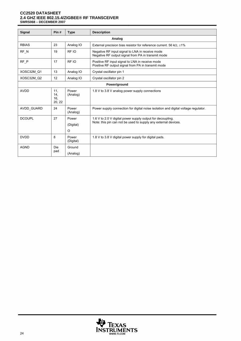
24 WWW.TI.COM
Signal Pin # Type Description
Analog
RBIAS 23 Analog IO External precision bias resistor for reference current. 56 kΩ, ±1%
RF_N 19 RF IO Negative RF input signal to LNA in receive mode Negative RF output signal from PA in transmit mode
RF_P 17 RF IO Positive RF input signal to LNA in receive mode Positive RF output signal from PA in transmit mode
XOSC32M_Q1 13 Analog IO Crystal oscillator pin 1
XOSC32M_Q2 12 Analog IO Crystal oscillator pin 2
Power/ground
AVDD 11, 14, 16, 20, 22
Power (Analog)
1.8 V to 3.8 V analog power supply connections
AVDD_GUARD 24 Power (Analog)
Power supply connection for digital noise isolation and digital voltage regulator.
DCOUPL 27 Power
(Digital)
O
1.6 V to 2.0 V digital power supply output for decoupling. Note: this pin can not be used to supply any external devices.
DVDD 8 Power (Digital)
1.8 V to 3.8 V digital power supply for digital pads.
AGND Die pad
Ground
(Analog)
CC2520 DATASHEET2.4 GHZ IEEE 802.15.4/ZIGBEE® RF TRANSCEIVER
SWRS068 – DECEMBER 2007
WWW.TI.COM 25
8 Functional Introduction
8.1 Integrated 2.4 GHz IEEE 802.15.4 Compliant Radio
CC2520 features a Direct Conversion Transceiver operating in the 2.4 GHz band with excellent receiver sensitivity and robustness to interferers. The CC2520 radio complies with the IEEE 802.15.4 PHY specification. The radio has 250 kbps data rate, 2 Mchip/s chip rate, and is suitable for systems targeting compliance with worldwide radio frequency regulations covered by ETSI EN 300 328 and EN 300 440 class 2 (Europe), FCC CFR47 Part 15 (US) and ARIB STD-T66 (Japan).
8.2 Comparison to CC2420
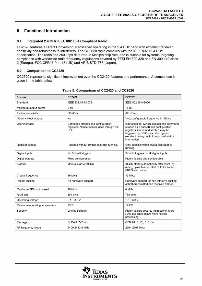
CC2520 represents significant improvement over the CC2420 features and performance. A comparison is given in the table below.
Table 5: Comparison of CC2420 and CC2520
Feature CC2420 CC2520
Standard IEEE 802.15.4-2003 IEEE 802.15.4-2006
Maximum output power 0 dB +5 dB
Typical sensitivity -95 dBm -98 dBm
General clock output No Yes, configurable frequency 1-16MHz
User interface Command strobes and configuration registers. All user control goes through the SPI.
Instruction set (which includes the command strobes as a subset) and configuration registers. Command strobes may be triggered by GPIO pins, which gives excellent timing control. Improved status information.
Register access Possible without crystal oscillator running. Only possible when crystal oscillator is running.
Digital inputs No Schmitt triggers Schmitt triggers on all digital inputs.
Digital outputs Fixed configuration Highly flexible and configurable
Start up Manual start of XOSC XOSC starts automatically after reset (by reset_n pin). Manual start of XOSC after SRES instruction.
Crystal frequency 16 MHz 32 MHz
Packet sniffing No hardware support Hardware support for non-intrusive sniffing of both transmitted and received frames.
Maximum SPI clock speed 10 MHz 8 MHz
RAM size 364 byte 768 byte
Operating voltage 2.1 – 3.6 V 1.8 – 3.8 V
Maximum operating temperature 85°C 125°C
Security Limited flexibility Highly flexible security instructions. More RAM available allows more flexible processing.
Package QLP-48, 7x7 mm QFN 28 (RHD), 5x5 mm
RF frequency range 2400-2483.5 MHz 2394-2507 MHz
CC2520 DATASHEET 2.4 GHZ IEEE 802.15.4/ZIGBEE® RF TRANSCEIVER SWRS068 – DECEMBER 2007
26 WWW.TI.COM
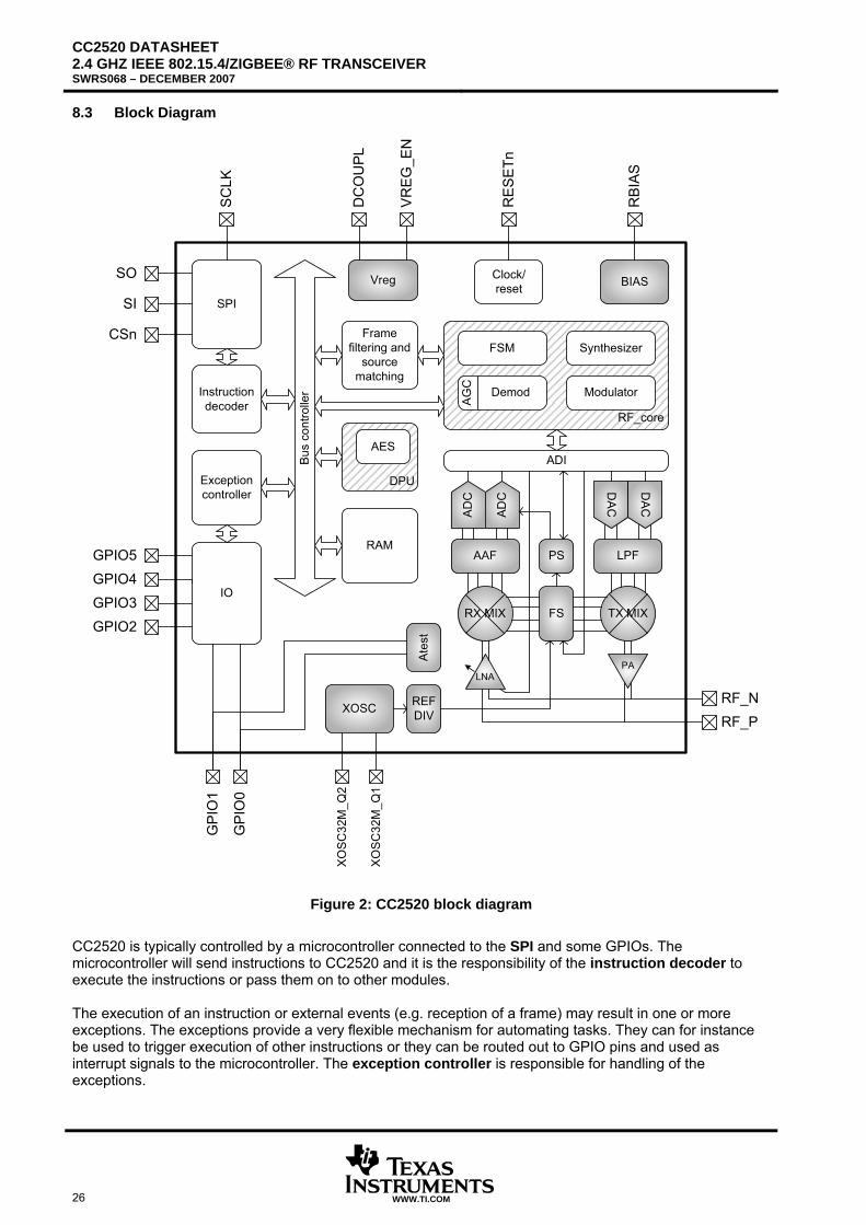
8.3 Block Diagram
RF_core
Framefiltering and
source matching
GPIO5
IO
SPI
Instruction decoder
Clock/reset
RAM
DPU
GPIO4GPIO3GPIO2
GP
IO1
GP
IO0
SO
SI
CSn
Exception controller
AD
C
ADC
DA
C
DA
C
LPF
TX MIX
PA
RX MIX
AAF
LNA
AES
Modulator
SynthesizerFSM
FS
REF DIVXOSC
XO
SC32
M_Q
2
XO
SC32
M_Q
1
Bus
cont
rolle
r
BIAS
SC
LK
RE
SE
Tn
RB
IAS
RF_NRF_P
ADI
Vreg
DC
OU
PL
VR
EG
_EN
Demod
AG
C
PS
ADI
Ate
st
Figure 2: CC2520 block diagram
CC2520 is typically controlled by a microcontroller connected to the SPI and some GPIOs. The microcontroller will send instructions to CC2520 and it is the responsibility of the instruction decoder to execute the instructions or pass them on to other modules. The execution of an instruction or external events (e.g. reception of a frame) may result in one or more exceptions. The exceptions provide a very flexible mechanism for automating tasks. They can for instance be used to trigger execution of other instructions or they can be routed out to GPIO pins and used as interrupt signals to the microcontroller. The exception controller is responsible for handling of the exceptions.
CC2520 DATASHEET2.4 GHZ IEEE 802.15.4/ZIGBEE® RF TRANSCEIVER
SWRS068 – DECEMBER 2007
WWW.TI.COM 27
The microcontroller will typically be connected to one or more of the GPIO pins. The function of each pin is independently controlled by the IO module based on register settings. It is possible to observe a large number of internal signals on the GPIO pins. The GPIO pins can also be configured as inputs and used to trigger the execution of certain instructions. This would typically be used when the microcontroller needs to precisely control the timing of an instruction. The RAM module contains memory which is used for receive and transmit FIFOs (in fixed address ranges) and temporary storage for other data. There are separate instructions for general memory access and FIFO access. The data processing unit (DPU) is responsible for execution of the more advanced instructions. The DPU includes an AES core, which is used while executing the security instructions. Memory management (copying, incrementing etc.) is also performed by the DPU. The Clock/Reset module generates the internal clocks and reset signals. The RF core contains several submodules that support and control the analog radio modules. The FSM submodule controls the RF transceiver state, the transmitter and receiver FIFOs and most of the dynamically controlled analog signals such as power up / down of analog modules. The FSM is used to provide the correct sequencing of events (such as performing an FS calibration before enabling the receiver). Also, it provides step by step processing of incoming frames from the demodulator: reading the frame length, counting the number of bytes received, checks the FCS, and finally, optionally handles automatic transmission of ACK frames after successful frame reception. It performs similar tasks in TX including performing an optional CCA before transmission and automatically going to RX after the end of transmission to receive an ACK frame. Finally, the FSM controls the transfer of data between modulator/demodulator and the TXFIFO/RXFIFO in RAM. The modulator transforms raw data into I/Q signals to the transmitter DAC. This is done in compliance with the IEEE 802.15.4 standard. The demodulator is responsible for retrieving the sent data from the received signal. The amplitude information from the demodulator is used by the automatic gain control (AGC). The AGC adjusts the gain of the analog LNA so that the signal level within the receiver is approximately constant.. The frame filtering and source matching supports the FSM in RF_core by performing all operations needed in order to do frame filtering and source address matching, as defined by IEEE 802.15.4. The xosc module interfaces the crystal which is connected to the XOSC32M_Q1 and XOSC32M_Q2 pins. The xosc module generates a clock for the digital part and RF system, and implements the programmable crystal frequency tuning. The BIAS module generates voltage and current references. It relies on a high precision (1%) 56kΩ external resistor which is shown in the application circuit in Figure 3. The TX DACs convert the digital baseband signal to analog signals. After LPF the signal is fed to the TXMIX module, which is an up-converting complex mixer. The PA amplifies the RF signal up to a maximum of ~5dBm during TX. The LNA amplifies the received RF signal. The gain is controlled by the digital AGC module so that optimum sensitivity and interferer rejection is achieved. The RXMIX module is a complex down-mixer that converts the RF signal to a baseband signal. A passive anti-aliasing filter (AAF) low pass filters the signal after down mixing. The low pass filtered I and Q signals and digitized by the ADC.

CC2520 DATASHEET 2.4 GHZ IEEE 802.15.4/ZIGBEE® RF TRANSCEIVER SWRS068 – DECEMBER 2007
28 WWW.TI.COM
The frequency synthesizer (FS) generates the carrier wave for the RF signal. The voltage regulator (Vreg) provides a 1.8V supply voltage to the digital core. It contains a current limiter, which is enabled for currents above ~32mA.
CC2520 DATASHEET2.4 GHZ IEEE 802.15.4/ZIGBEE® RF TRANSCEIVER
SWRS068 – DECEMBER 2007
WWW.TI.COM 29
9 Application Circuit Very few external components are required for the operation of CC2520. A typical application circuit is shown in Figure 4. Note that it does not show how the board layout should be done. The board layout will greatly influence the RF performance of CC2520. This section is meant as an introduction only. For further details, see the reference design, which includes complete board layouts and bill of materials with manufacturer and part numbers. The reference design can be downloaded from the CC2520 product folder [7]. Note that decoupling capacitors are not shown in the figure below. See the reference design for complete bill of materials.
8 9 10 11 12 13 14
28 27 26 25 24 23 22
DVD
D
GP
IO1
GP
IO0
AVD
D5
XOSC
32M
_Q2
XOSC
32M
_Q1
AVD
D3
SC
LK
DC
OU
PL
VR
EG
_EN
RES
ETn
AVD
D_G
UAR
D
RBI
AS
AVD
D4
Dig
ital i
nter
face
Figure 3: Typical application circuit with transmission line balun for single-ended operation
See the antenna selection guide [12] for further details on other compact and low-cost alternatives.
9.1 Input / Output Matching
The RF input/output is high impedance and differential. When using an unbalanced antenna such as a monopole, a balun should be used in order to optimize performance. The balun can be implemented using low-cost discrete inductors and capacitors only or in combination with transmission lines replacing the discrete inductors. Figure 4 shows the balun implemented in a two-layer reference design. It consists of three transmission lines (L1, L2 and L3) and the discrete components C191, C171, C192, C173 and C174. The circuit will present the optimum RF termination to CC2520 with a 50Ω load on the antenna connection.
CC2520 DATASHEET 2.4 GHZ IEEE 802.15.4/ZIGBEE® RF TRANSCEIVER SWRS068 – DECEMBER 2007
30 WWW.TI.COM
C19
1C
171
C172C
192
C173 C174
R201
SMA connector
PCB antenna
CC
2520
Figure 4: Actual board layout of the RF section of the reference design (rev 2.1).
9.2 Bias Resistor
The bias resistor R231 is used to set an accurate bias current. A high precision (±1%) 56kΩ resistor should be used.
9.3 Crystal
An external 32MHz crystal with two loading capacitors (C121 and C131) is used for the crystal oscillator. It is possible to feed a single-ended signal to the XOSC32M_Q1 pin and thus not use a crystal.
9.4 Digital Voltage Regulator
The on chip voltage regulator supplies 1.8 V to the digital part of CC2520. C271 is a decoupling capacitor for the voltage regulator. Note that this should not be used to provide power to other IC’s.
9.5 Power Supply Decoupling and Filtering
Proper power supply decoupling must be used for optimum performance. This is shown as a lumped capacitor C1 in Figure 4. The placement and size of the decoupling capacitors and the power supply filtering are very important to achieve the best performance in an application. TI provides a compact reference design that should be followed very closely.
9.6 Board Layout Guidelines
It is highly recommended to copy the board layout from the reference design [5].
• It is recommended to use star topology for the power supplies to CC2520. • The power supply decoupling capacitor C1 is a lumped component. On the actual board layout
there should be separate decoupling capacitors as close to each of the power pins as possible. • The balun is highly layout sensitive. The inductors in Figure 4 are actually transmission lines
embedded in the PCB and their values must be adapted according to the board layout. The values of the capacitors C192, C172, C173 and C174 must also be adapted to the actual board layout.
• The GPIO pins can be configured to use internal pull-up resistors. They are not enabled after a reset or in LPM2. Remember to take the default GPIO configuration into consideration when connecting these signals, because there will be some time before the MCU is able to change the configuration. In LPM2 GPIO5 (which is configured as an input) should be connected to either
CC2520 DATASHEET2.4 GHZ IEEE 802.15.4/ZIGBEE® RF TRANSCEIVER
SWRS068 – DECEMBER 2007
WWW.TI.COM 31
ground or VDD. The other GPIO pins should be grounded or high impedance. Failing to do this, will result in significantly higher current consumption than necessary.
• The SO pin is configured as an input when CSn is high or the device is in reset or LPM2. This makes it possible to connect multiple SPI slaves to one SPI master. This pin should not be left floating when in LPM2, as this will draw more current than necessary. If the voltage level can not be controlled in any other way, use a 1MOhm pull-down resistor.
• The crystal input lines should be routed as far away from each other as practically possible. • The NC pins can be left floating. • Glitches on the digital inputs may create serious issues in a system design. The digital input pads
have Schmitt-triggers to help make them less sensitive to glitches, but the board layout should still avoid routing the digital input lines close to other noisy signals.
9.7 Antenna Considerations
The reference design contains two antenna options. As default, the SMA connector is connected to the balun through a 0Ω resistor. This resistor can be soldered off and rotated 90° clockwise in order to connect to the PCB antenna, which is a planar inverted F antenna (PIFA). Note that all testing and characterization has been done using the SMA connector. The PCB antenna has only been functionally tested by establishing a link between two EMs. In our experiment, the PCB antenna gave approximately the same range as when using an antenna connected to the SMA connector. Please refer to the antenna selection guide [12] and the Inverted F antenna app note [11] for further details.
9.8 Choosing the Most Suitable Interconnection with a Microcontroller
• Connect the 4 SPI signals; CSn, SCLK, SI and SO to the microcontroller. These signals are required in order to configure CC2520 and exchange data with it.
• Connect RESETn to the microcontroller. Using the RESETn signal is the recommended way to reset CC2520 for instance after powering up. If saving a pin is critical, the RESETn pin can be connected to VDD. The CC2520 can still be reset with the SRES command strobe. This will also require a manual start of the crystal oscillator by issuing a SXOSCON command strobe.
• Connecting VREG_EN to the microcontroller will make it possible to put CC2520 into LPM2 to save power. VREG_EN may be connected to VDD and thus always leave the regulator on. If power saving is not important in the target application, this may be an acceptable way of saving a pin.
• Connecting one or more of the GPIOs to the microcontroller is optional. The number of GPIOs to connect depends on the application. Connecting more GPIOs to the microcontroller generally gives more flexibility and less SPI traffic because it reduces the need to keep reconfiguring the GPIOs for different uses.
• If CC2520 will be providing clock to the microcontroller, GPIO0 should be connected to the clock input of the microcontroller. After reset, GPIO0 will output a 1MHz clock signal with 50/50 duty cycle.
The digital IO of CC2520 is described in more detail from section 12.
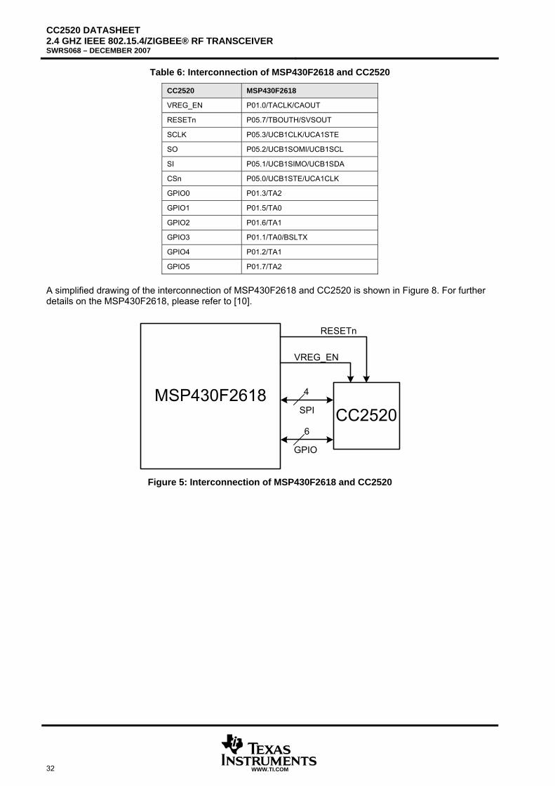
9.9 Interfacing CC2520 and MSP430F2618
The MSP430F2618 is well suited for use with the CC2520. The suggested interfacing of these two chips is given in Table 5. The interconnections shown in Table 6 are exactly the same as is used in the CC2520 development kit [5].
CC2520 DATASHEET 2.4 GHZ IEEE 802.15.4/ZIGBEE® RF TRANSCEIVER SWRS068 – DECEMBER 2007
32 WWW.TI.COM
Table 6: Interconnection of MSP430F2618 and CC2520
CC2520 MSP430F2618
VREG_EN P01.0/TACLK/CAOUT
RESETn P05.7/TBOUTH/SVSOUT
SCLK P05.3/UCB1CLK/UCA1STE
SO P05.2/UCB1SOMI/UCB1SCL
SI P05.1/UCB1SIMO/UCB1SDA
CSn P05.0/UCB1STE/UCA1CLK
GPIO0 P01.3/TA2
GPIO1 P01.5/TA0
GPIO2 P01.6/TA1
GPIO3 P01.1/TA0/BSLTX
GPIO4 P01.2/TA1
GPIO5 P01.7/TA2
A simplified drawing of the interconnection of MSP430F2618 and CC2520 is shown in Figure 8. For further details on the MSP430F2618, please refer to [10].
SPI
GPIO
RESETn
VREG_EN
4
6
Figure 5: Interconnection of MSP430F2618 and CC2520
CC2520 DATASHEET2.4 GHZ IEEE 802.15.4/ZIGBEE® RF TRANSCEIVER
SWRS068 – DECEMBER 2007
WWW.TI.COM 33
10 Serial Peripheral Interface (SPI) The SPI provides an interface for giving instructions to the CC2520 and transferring data between CC2520 and a microcontroller. The CC2520 4-wire slave interface consists of three input signals (CSn, SCLK and SI) and one output signal (SO). In section 15 all instructions available via the SPI interface are listed and described. The instructions are byte oriented and required bytes sent over the interface to CC2520 vary from 1 and up. To transfer one byte CSn must be pulled low and SCLK must complete 8 periods starting with a positive edge. There are no requirements to maximum period for SCLK or that it needs to be continuous. As long as CSn is held low, SCLK can be halted at any time and started again when desired.
10.1 CSn
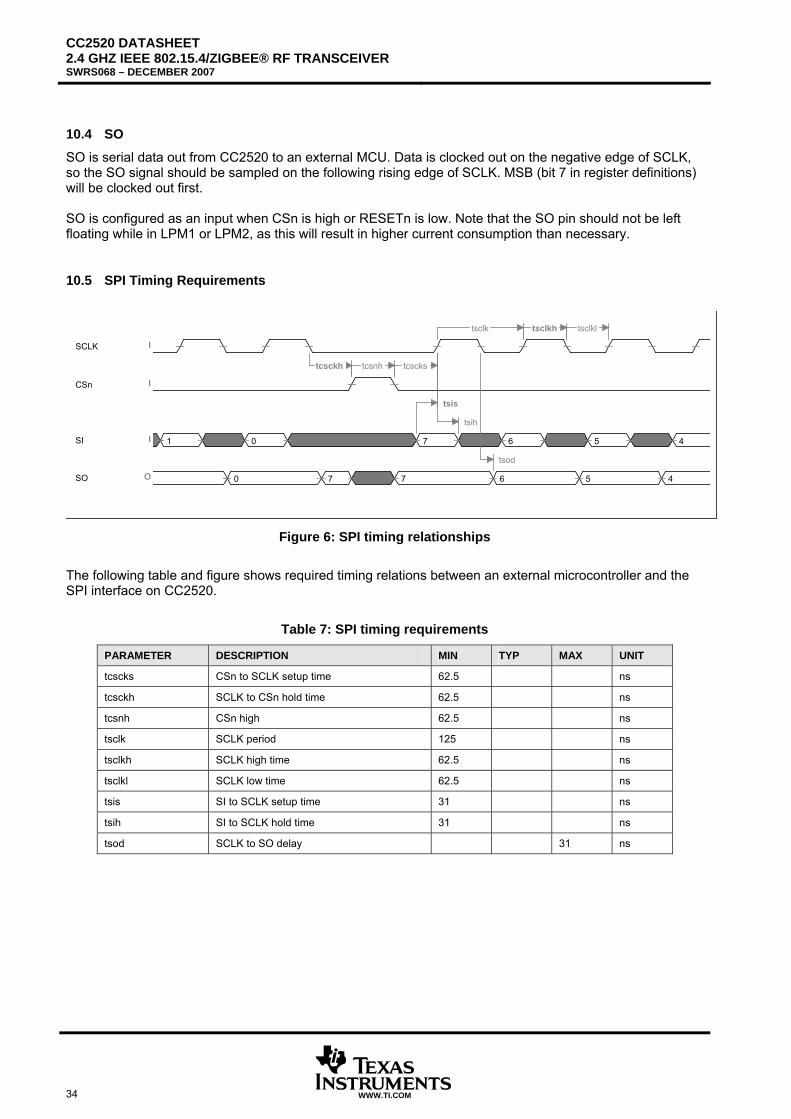
CSn is an input enable signal for the SPI and is controlled by the external MCU. The CSn signal is used as an asynchronous active high reset to the SPI module. CSn must be held low during all SPI operations and must also be held low for more than two periods of XOSC before the first positive edge of SCLK and more than two periods of XOSC after the last negative edge of SCLK. When CSn is high it must be held high for at least 2 periods of XOSC. CSn can be held low between SPI operations in the case where the last instruction completed has a constant number of bytes, but this will result in unnecessary power consumption since parts of the instruction controller will then be running. The instructions that have a constant number of bytes can be found in the instruction summary table in section 15.3. I.e. SRXON (1 byte) and RXMASKAND (3 bytes) has constant number of bytes and REGRD (2 bytes or more) has user controlled number of bytes indicated in the table by three dots (…) in the byte column after the last required byte of the instruction command (Byte 3 for REGRD). Instructions that have user controlled number of bytes are ended by rising CSn. Status is output as the first byte on SO during the first byte of all instructions. When instructions are transferred consecutively without rising CSn between them, the status byte on SO may not contain the correct current status. However, the status will be updated for the second byte of an instruction so i.e RXMASKAND which outputs status also during the second instruction byte will then output the correct status during the second byte. When pulling CSn low after power-up, SO outputs the internal XOSC stable signal combinatorically, so no edge on SCLK is necessary to find the XOSC stable status. In any case where CSn is pulled low and SO is low it means that XOSC is still not stable and thus there is no clock in the digital part. The maximum time from power up to XOSC should be stable is described in section 5.3.
10.2 SCLK
SCLK is controlled by an external MCU and is an input clock to CC2520. SCLK is asynchronous to the internal XOSC clock in CC2520. The maximum SCLK frequency is 8 MHz. There is no minimum frequency requirement.
10.3 SI
SI is the serial data input from the microcontroller to CC2520. Data shall be sent with MSB first (bit 7 in each byte of instruction commands). Data should be set up on the negative edge of SCLK and will be clocked into CC2520 by the next positive edge of SCLK.
CC2520 DATASHEET 2.4 GHZ IEEE 802.15.4/ZIGBEE® RF TRANSCEIVER SWRS068 – DECEMBER 2007
34 WWW.TI.COM
10.4 SO
SO is serial data out from CC2520 to an external MCU. Data is clocked out on the negative edge of SCLK, so the SO signal should be sampled on the following rising edge of SCLK. MSB (bit 7 in register definitions) will be clocked out first. SO is configured as an input when CSn is high or RESETn is low. Note that the SO pin should not be left floating while in LPM1 or LPM2, as this will result in higher current consumption than necessary.
10.5 SPI Timing Requirements
SCLK I
CSn I
SI I
SO O
1 0 7 6 5 4
0 7 7 6 5 4
tcsckstcsnh
tsclk
tsih
tsis
tcsckh
tsclkh
tsod
tsclkl
Figure 6: SPI timing relationships
The following table and figure shows required timing relations between an external microcontroller and the SPI interface on CC2520.
Table 7: SPI timing requirements
PARAMETER DESCRIPTION MIN TYP MAX UNIT
tcscks CSn to SCLK setup time 62.5 ns
tcsckh SCLK to CSn hold time 62.5 ns
tcsnh CSn high 62.5 ns
tsclk SCLK period 125 ns
tsclkh SCLK high time 62.5 ns
tsclkl SCLK low time 62.5 ns
tsis SI to SCLK setup time 31 ns
tsih SI to SCLK hold time 31 ns
tsod SCLK to SO delay 31 ns
CC2520 DATASHEET2.4 GHZ IEEE 802.15.4/ZIGBEE® RF TRANSCEIVER
SWRS068 – DECEMBER 2007
WWW.TI.COM 35
11 GPIO CC2520 has 6 GPIO pins that can be individually configured as inputs, outputs and activate pull-up resistors. Each GPIO has an associated register, GPIOCTRLn, where the MSB configure the pin to either input or output. The GPIOCTRL register control pull-up for each individual GPIO pin, extra drive strength for all pins and analog function for pin 0 and 1. See section 30 for details about test functionality and observability through GPIO. Note that GPIO5, which is configured as an input in LPM2, should be tied either to ground or VDD when entering LPM2. If GPIO5 (or any other input) is left floating, the current consumption will be unpredictable.
11.1 Reset Configuration of GPIO Pins
The reset setting for GPIO pins are as shown in the table below. This is also the configuration that is used when the device is in LPM2. If a different GPIO setup is required, the GPIOs have to be re-configured every time CC2520 has been in LPM2. This particular reset configuration was selected so that CC2520 looks as much like CC2420 as possible.
Table 8: GPIO reset state
GPIO pin
Dir Value Pull up
Extra drive
Polarity Signal GPIOCTRLn value (hex)
Description
0 Out 0 No No Positive clock 0x00 1MHz clock signal with 50/50 duty cycle.
1 Out 0 No No Positive fifo 0x27 High when one or more bytes are in the RX FIFO. Low during RX FIFO overflow.
2 Out 0 No No Positive fifop 0x28 High when the number of bytes in the RX FIFO exceeds the programmable threshold or at least one complete frame is in the RX FIFO. Also high during RX FIFO overflow.
3 Out 0 No No Positive cca 0x29 Clear channel assessment. See FSMSTAT1 register for details on how to configure the behavior of this signal.
4 Out 0 No No Positive sfd 0x2A Pin is high when SFD has been received or transmitted. Cleared when leaving RX/TX respectively.
5 In Tie to ground or VDD
No No Positive 0x90 No function
11.2 GPIO as Input
When configured as input, the GPIO pin can be used to trigger one of 16 different command strobes (See section 15) as shown in the GPIO configuration table in section 12.6. These command strobes are a subset of all the SPI instructions available. The command strobe is triggered by applying a rising or falling edge to the GPIO pin depending on the setting in the GPIOPOLARITY register. Which command strobe the pin triggers is set by the 7 LSBs in GPIOCTRLn. Example: Set up GPIO2 to run SACK instruction on rising edge.
• Set GPIOPOLARITY[2] to ‘1’. GPIO pin 2 set to rising edge active. • Set GPOICTRL2[7:0] to “1000 0101” . GPIO pin 2 is now an input and connected to the SACK
instruction.
CC2520 DATASHEET 2.4 GHZ IEEE 802.15.4/ZIGBEE® RF TRANSCEIVER SWRS068 – DECEMBER 2007
36 WWW.TI.COM
11.3 GPIO as Output
When a GPIO pin is configured as an output, the signal corresponding to the CTRLn setting in GPIOCTRLn register (CTRLn values are shown in Table 8 in section 12.6). The polarity of the pin is set in the GPIOPOLARITY register. Example: Set up GPIO3 to output sniff_data with active high level indication.
• Set GPIOPOLARITY[3] to ‘1’’. GPIO pin 3 set to active high level indication. • Set GPIOCTRL3[7:0] to “0011 0010”. GPIO pin 3 is now an output and outputs sniff_data.
11.4 Switching Direction on GPIO
When switching from output to input, care must be taken so that command strobes are not triggered unintentionally. Changing GPIOn to a command strobe triggering input (one of the first 16 entries in Table 8) needs to be done using the following procedure to avoid changing direction while the pin is high:
1. Write 0x7E to GPIOCTRLn to make it output a constant 0. 2. Drive a ‘0’ from the microcontroller to the GPIO pin. 3. Write for instance 0x88 to GPIOCTRLn to change to input that triggers the STXON command
strobe.
11.5 GPIO Configuration
Table 8 summarizes the signals that are available as output on any GPIO pin. The CTRLn column shows the configuration value that needs to be written to any one of the GPIOCTRL0-GPIOCTRL5 registers in order to get the described functionality. The IN column in Table 8 shows which command strobe that will be executed if the GPIO is configured as input and an edge (with the correct polarity) is applied. The OUT column shows the name of the internal signal that is observable on the pin if the GPIO is configured as an output.
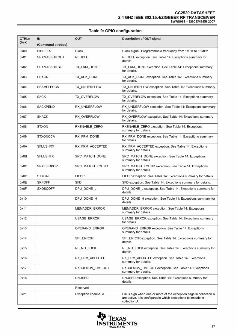
CC2520 DATASHEET2.4 GHZ IEEE 802.15.4/ZIGBEE® RF TRANSCEIVER
SWRS068 – DECEMBER 2007
WWW.TI.COM 37
Table 9: GPIO configuration
CTRLn (hex)
IN
(Command strobes)
OUT Description of OUT signal
0x00 SIBUFEX Clock Clock signal. Programmable frequency from 1MHz to 16MHz
0x01 SRXMASKBITCLR RF_IDLE RF_IDLE exception. See Table 14: Exceptions summary for details.
0x02 SRXMASKBITSET TX_FRM_DONE TX_FRM_DONE exception. See Table 14: Exceptions summary for details.
0x03 SRXON TX_ACK_DONE TX_ACK_DONE exception. See Table 14: Exceptions summary for details.
0x04 SSAMPLECCA TX_UNDERFLOW TX_UNDERFLOW exception. See Table 14: Exceptions summary for details.
0x05 SACK TX_OVERFLOW TX_OVERFLOW exception. See Table 14: Exceptions summary for details.
0x06 SACKPEND RX_UNDERFLOW RX_UNDERFLOW exception. See Table 14: Exceptions summary for details.
0x07 SNACK RX_OVERFLOW RX_OVERFLOW exception. See Table 14: Exceptions summary for details.
0x08 STXON RXENABLE_ZERO RXENABLE_ZERO exception. See Table 14: Exceptions summary for details.
0x09 STXONCCA RX_FRM_DONE RX_FRM_DONE exception. See Table 14: Exceptions summary for details.
0x0A SFLUSHRX RX_FRM_ACCEPTED RX_FRM_ACCEPTED exception. See Table 14: Exceptions summary for details.
0x0B SFLUSHTX SRC_MATCH_DONE SRC_MATCH_DONE exception. See Table 14: Exceptions summary for details.
0x0C SRXFIFOPOP SRC_MATCH_FOUND SRC_MATCH_FOUND exception. See Table 14: Exceptions summary for details.
0x0D STXCAL FIFOP FIFOP exception. See Table 14: Exceptions summary for details.
0x0E SRFOFF SFD SFD exception. See Table 14: Exceptions summary for details.
0x0F SXOSCOFF DPU_DONE_L DPU_DONE_L exception. See Table 14: Exceptions summary for details.
0x10 DPU_DONE_H DPU_DONE_H exception. See Table 14: Exceptions summary for details.
0x11 MEMADDR_ERROR MEMADDR_ERROR exception. See Table 14: Exceptions summary for details.
0x12 USAGE_ERROR USAGE_ERROR exception. See Table 14: Exceptions summary for details.
0x13 OPERAND_ERROR OPERAND_ERROR exception. See Table 14: Exceptions summary for details.
0x14 SPI_ERROR SPI_ERROR exception. See Table 14: Exceptions summary for details.
0x15 RF_NO_LOCK RF_NO_LOCK exception. See Table 14: Exceptions summary for details.
0x16 RX_FRM_ABORTED RX_FRM_ABORTED exception. See Table 14: Exceptions summary for details.
0x17 RXBUFMOV_TIMEOUT RXBUFMOV_TIMEOUT exception. See Table 14: Exceptions summary for details.
0x18 UNUSED UNUSED exception. See Table 14: Exceptions summary for details.
... Reserved
0x21 Exception channel A Pin is high when one or more of the exception flags in collection A are active. It is configurable which exceptions to include in collection A.
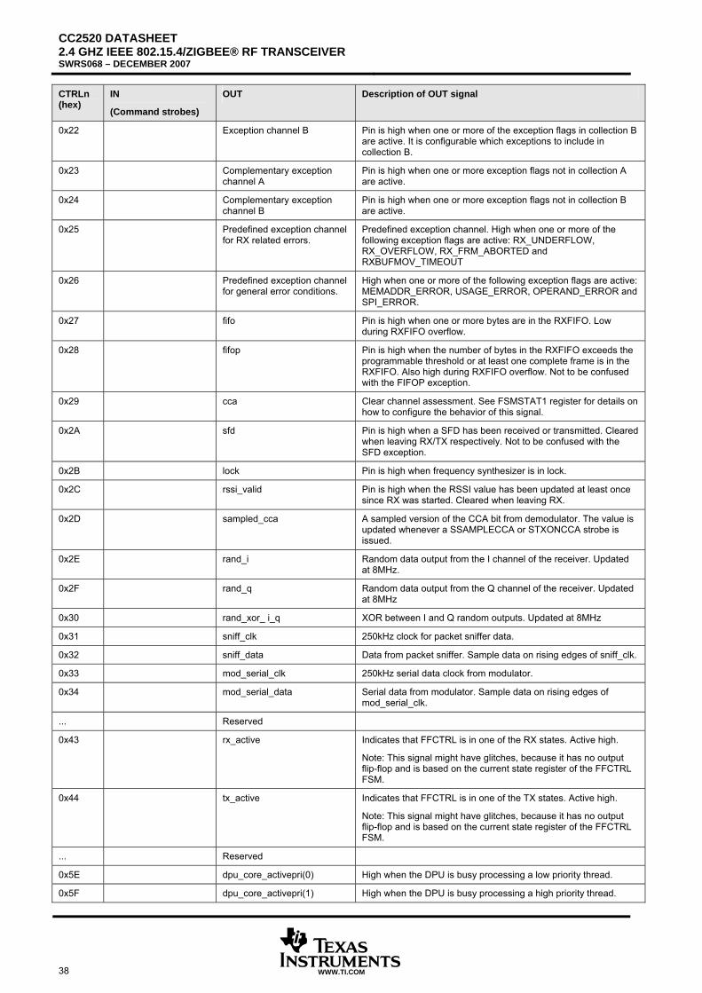
CC2520 DATASHEET 2.4 GHZ IEEE 802.15.4/ZIGBEE® RF TRANSCEIVER SWRS068 – DECEMBER 2007
38 WWW.TI.COM
CTRLn (hex)
IN
(Command strobes)
OUT Description of OUT signal
0x22 Exception channel B Pin is high when one or more of the exception flags in collection B are active. It is configurable which exceptions to include in collection B.
0x23 Complementary exception channel A
Pin is high when one or more exception flags not in collection A are active.
0x24 Complementary exception channel B
Pin is high when one or more exception flags not in collection B are active.
0x25 Predefined exception channel for RX related errors.
Predefined exception channel. High when one or more of the following exception flags are active: RX_UNDERFLOW, RX_OVERFLOW, RX_FRM_ABORTED and RXBUFMOV_TIMEOUT
0x26 Predefined exception channel for general error conditions.
High when one or more of the following exception flags are active: MEMADDR_ERROR, USAGE_ERROR, OPERAND_ERROR and SPI_ERROR.
0x27 fifo Pin is high when one or more bytes are in the RXFIFO. Low during RXFIFO overflow.
0x28 fifop Pin is high when the number of bytes in the RXFIFO exceeds the programmable threshold or at least one complete frame is in the RXFIFO. Also high during RXFIFO overflow. Not to be confused with the FIFOP exception.
0x29 cca Clear channel assessment. See FSMSTAT1 register for details on how to configure the behavior of this signal.
0x2A sfd Pin is high when a SFD has been received or transmitted. Cleared when leaving RX/TX respectively. Not to be confused with the SFD exception.
0x2B lock Pin is high when frequency synthesizer is in lock.
0x2C rssi_valid Pin is high when the RSSI value has been updated at least once since RX was started. Cleared when leaving RX.
0x2D sampled_cca A sampled version of the CCA bit from demodulator. The value is updated whenever a SSAMPLECCA or STXONCCA strobe is issued.
0x2E rand_i Random data output from the I channel of the receiver. Updated at 8MHz.
0x2F rand_q Random data output from the Q channel of the receiver. Updated at 8MHz
0x30 rand_xor_ i_q XOR between I and Q random outputs. Updated at 8MHz
0x31 sniff_clk 250kHz clock for packet sniffer data.
0x32 sniff_data Data from packet sniffer. Sample data on rising edges of sniff_clk.
0x33 mod_serial_clk 250kHz serial data clock from modulator.
0x34 mod_serial_data Serial data from modulator. Sample data on rising edges of mod_serial_clk.
... Reserved
0x43 rx_active Indicates that FFCTRL is in one of the RX states. Active high.
Note: This signal might have glitches, because it has no output flip-flop and is based on the current state register of the FFCTRL FSM.
0x44 tx_active Indicates that FFCTRL is in one of the TX states. Active high.
Note: This signal might have glitches, because it has no output flip-flop and is based on the current state register of the FFCTRL FSM.
... Reserved
0x5E dpu_core_activepri(0) High when the DPU is busy processing a low priority thread.
0x5F dpu_core_activepri(1) High when the DPU is busy processing a high priority thread.

CC2520 DATASHEET2.4 GHZ IEEE 802.15.4/ZIGBEE® RF TRANSCEIVER
SWRS068 – DECEMBER 2007
WWW.TI.COM 39
CTRLn (hex)
IN
(Command strobes)
OUT Description of OUT signal
... Reserved
0x62 dpu_state_l_active High when low priority thread is pending or active.
0x63 dpu_state_h_active High when high priority thread is pending or active.
… Reserved
0x7E ‘0’ Constant value
0x7F ‘1’ Constant value
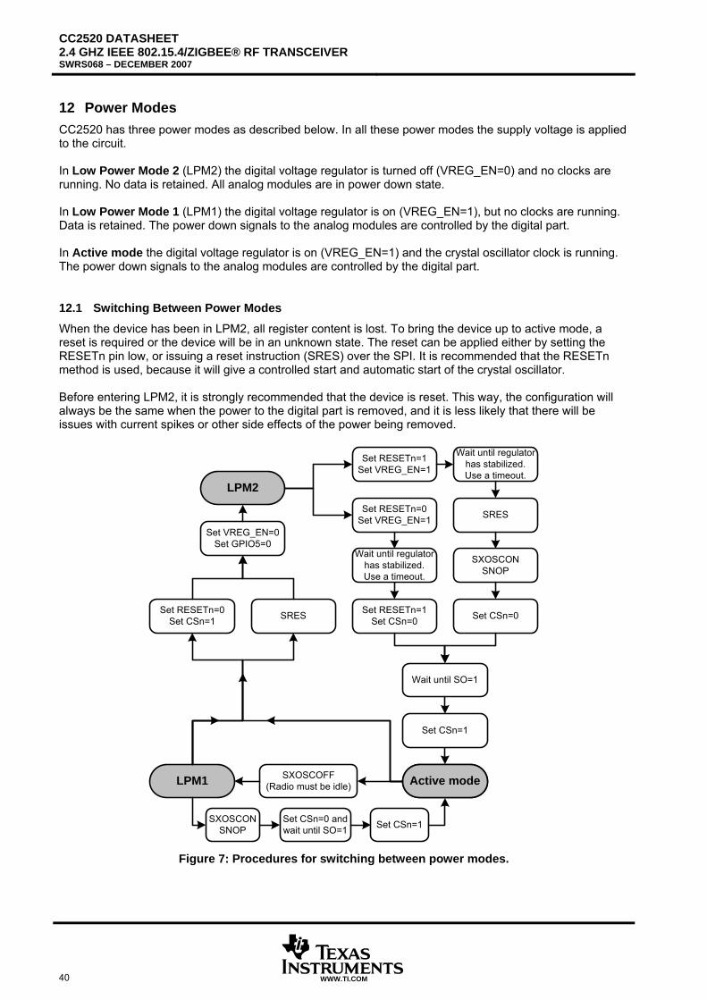
CC2520 DATASHEET 2.4 GHZ IEEE 802.15.4/ZIGBEE® RF TRANSCEIVER SWRS068 – DECEMBER 2007
40 WWW.TI.COM
12 Power Modes CC2520 has three power modes as described below. In all these power modes the supply voltage is applied to the circuit. In Low Power Mode 2 (LPM2) the digital voltage regulator is turned off (VREG_EN=0) and no clocks are running. No data is retained. All analog modules are in power down state. In Low Power Mode 1 (LPM1) the digital voltage regulator is on (VREG_EN=1), but no clocks are running. Data is retained. The power down signals to the analog modules are controlled by the digital part. In Active mode the digital voltage regulator is on (VREG_EN=1) and the crystal oscillator clock is running. The power down signals to the analog modules are controlled by the digital part.
12.1 Switching Between Power Modes
When the device has been in LPM2, all register content is lost. To bring the device up to active mode, a reset is required or the device will be in an unknown state. The reset can be applied either by setting the RESETn pin low, or issuing a reset instruction (SRES) over the SPI. It is recommended that the RESETn method is used, because it will give a controlled start and automatic start of the crystal oscillator. Before entering LPM2, it is strongly recommended that the device is reset. This way, the configuration will always be the same when the power to the digital part is removed, and it is less likely that there will be issues with current spikes or other side effects of the power being removed.
Active mode
Set RESETn=0Set VREG_EN=1
Set RESETn=1Set CSn=0
Wait until SO=1
Wait until regulator has stabilized. Use a timeout.
SXOSCOFF(Radio must be idle)
SXOSCONSNOP
Set RESETn=0Set CSn=1
Set VREG_EN=0Set GPIO5=0
LPM1
LPM2
Set RESETn=1 Set VREG_EN=1
Wait until regulator has stabilized. Use a timeout.
SRES
SXOSCONSNOP
Set CSn=0
Active mode
SRES
Set CSn=0 andwait until SO=1
Set CSn=1
Set CSn=1
Figure 7: Procedures for switching between power modes.
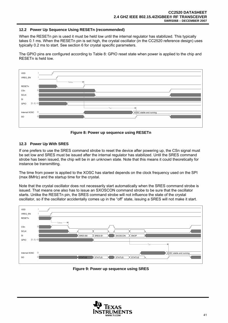
CC2520 DATASHEET2.4 GHZ IEEE 802.15.4/ZIGBEE® RF TRANSCEIVER
SWRS068 – DECEMBER 2007
WWW.TI.COM 41
12.2 Power Up Sequence Using RESETn (recommended)
When the RESETn pin is used it must be held low until the internal regulator has stabilized. This typically takes 0.1 ms. When the RESETn pin is set high, the crystal oscillator (in the CC2520 reference design) uses typically 0.2 ms to start. See section 6 for crystal specific parameters. The GPIO pins are configured according to Table 8: GPIO reset state when power is applied to the chip and RESETn is held low.
VDD I
VREG_EN I
RESETn I
CSn O
SCLK I
SI I
GPIO IO[5..0]
Internal XOSC O
SO O
XOSC stable and running
Txr
Tdres
Figure 8: Power up sequence using RESETn
12.3 Power Up With SRES
If one prefers to use the SRES command strobe to reset the device after powering up, the CSn signal must be set low and SRES must be issued after the internal regulator has stabilized. Until the SRES command strobe has been issued, the chip will be in an unknown state. Note that this means it could theoretically for instance be transmitting. The time from power is applied to the XOSC has started depends on the clock frequency used on the SPI (max 8MHz) and the startup time for the crystal. Note that the crystal oscillator does not necessarily start automatically when the SRES command strobe is issued. That means one also has to issue an SXOSCON command strobe to be sure that the oscillator starts. Unlike the RESETn pin, the SRES command strobe will not influence the state of the crystal oscillator, so if the oscillator accidentally comes up in the “off” state, issuing a SRES will not make it start.
VDD I
VREG_EN I
RESETn I
CSn O
SCLK I
SI I
GPIO IO[5..0]
Internal XOSC O
SO O
SRES B0 SRES B1 SXOSCON SNOP
XOSC stable and running
STATUS STATUS STATUS STATUS
Txr
Tdres
Figure 9: Power up sequence using SRES

CC2520 DATASHEET 2.4 GHZ IEEE 802.15.4/ZIGBEE® RF TRANSCEIVER SWRS068 – DECEMBER 2007
42 WWW.TI.COM
Table 10: Start-up Timing
Name Description Time
Tdres Time required after VREG_EN is activated until RESETn is released or CSn is set low.
≥ 0.1 ms
Txr Time for internal XOSC to stabilize after RESETn is released or SXOSCON strobe is issued.
0.2 ms (crystal dependent)
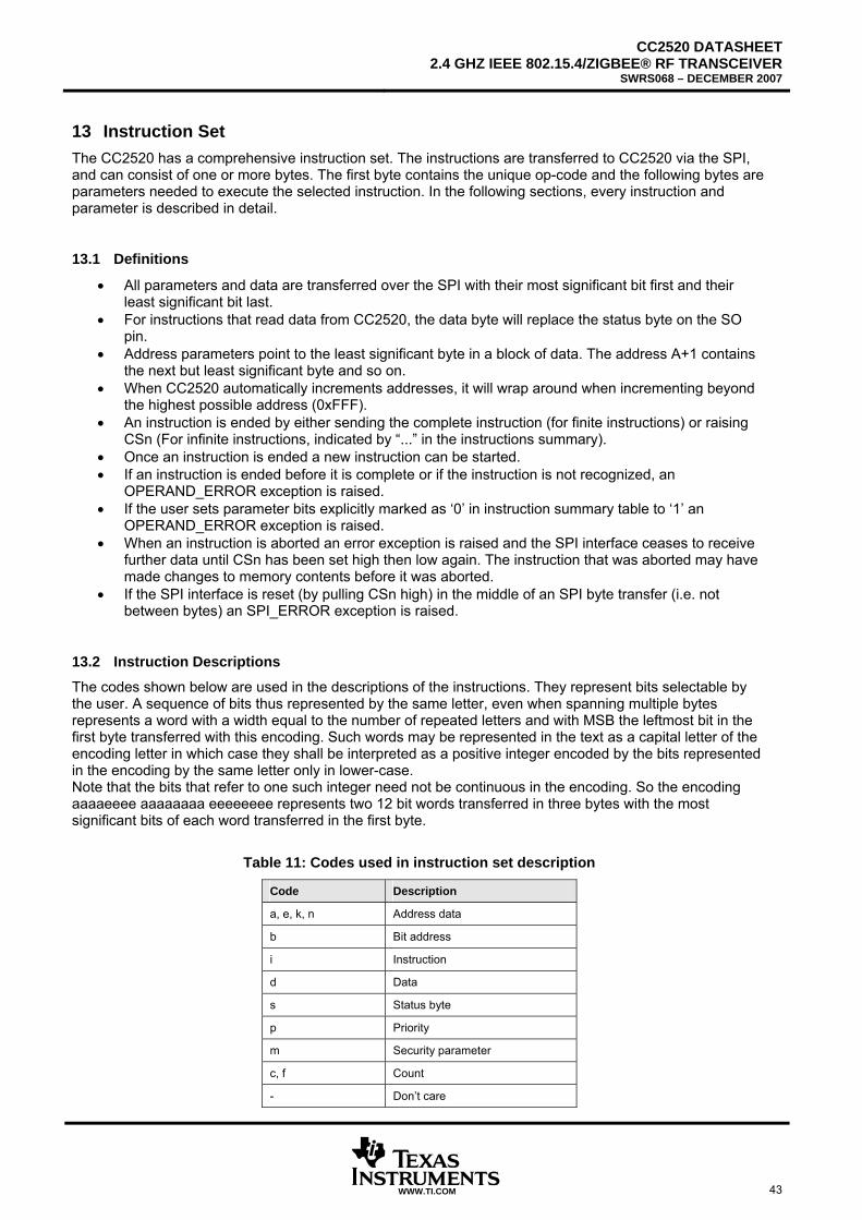
CC2520 DATASHEET2.4 GHZ IEEE 802.15.4/ZIGBEE® RF TRANSCEIVER
SWRS068 – DECEMBER 2007
WWW.TI.COM 43
13 Instruction Set The CC2520 has a comprehensive instruction set. The instructions are transferred to CC2520 via the SPI, and can consist of one or more bytes. The first byte contains the unique op-code and the following bytes are parameters needed to execute the selected instruction. In the following sections, every instruction and parameter is described in detail.
13.1 Definitions
• All parameters and data are transferred over the SPI with their most significant bit first and their least significant bit last.
• For instructions that read data from CC2520, the data byte will replace the status byte on the SO pin.
• Address parameters point to the least significant byte in a block of data. The address A+1 contains the next but least significant byte and so on.
• When CC2520 automatically increments addresses, it will wrap around when incrementing beyond the highest possible address (0xFFF).
• An instruction is ended by either sending the complete instruction (for finite instructions) or raising CSn (For infinite instructions, indicated by “...” in the instructions summary).
• Once an instruction is ended a new instruction can be started. • If an instruction is ended before it is complete or if the instruction is not recognized, an
OPERAND_ERROR exception is raised. • If the user sets parameter bits explicitly marked as ‘0’ in instruction summary table to ‘1’ an
OPERAND_ERROR exception is raised. • When an instruction is aborted an error exception is raised and the SPI interface ceases to receive
further data until CSn has been set high then low again. The instruction that was aborted may have made changes to memory contents before it was aborted.
• If the SPI interface is reset (by pulling CSn high) in the middle of an SPI byte transfer (i.e. not between bytes) an SPI_ERROR exception is raised.
13.2 Instruction Descriptions
The codes shown below are used in the descriptions of the instructions. They represent bits selectable by the user. A sequence of bits thus represented by the same letter, even when spanning multiple bytes represents a word with a width equal to the number of repeated letters and with MSB the leftmost bit in the first byte transferred with this encoding. Such words may be represented in the text as a capital letter of the encoding letter in which case they shall be interpreted as a positive integer encoded by the bits represented in the encoding by the same letter only in lower-case. Note that the bits that refer to one such integer need not be continuous in the encoding. So the encoding aaaaeeee aaaaaaaa eeeeeeee represents two 12 bit words transferred in three bytes with the most significant bits of each word transferred in the first byte.
Table 11: Codes used in instruction set description
Code Description
a, e, k, n Address data
b Bit address
i Instruction
d Data
s Status byte
p Priority
m Security parameter
c, f Count
- Don’t care
CC2520 DATASHEET 2.4 GHZ IEEE 802.15.4/ZIGBEE® RF TRANSCEIVER SWRS068 – DECEMBER 2007
44 WWW.TI.COM
Table 12: CC2520 instruction set
OPCODE Inputs Outputs Description Possible exceptions
Peripheral instructions
IBUFLD i[7:0]
s[7:0] Load instruction into instruction buffer. The instruction buffer holds a single instruction 1 byte long. The instruction to be loaded, I, is held and shall be parsed as a normal instruction when SIBUFEX is executed as if those bytes had just been transferred to the SPI interface.
Once the instruction held in the instruction buffer is executed it is replaced by SNOP.
SIBUFEX
Command strobe
s[7:0]
Execute the instruction stored in the instruction buffer as though those bytes had been transferred on the SPI interface.
A USAGE_ERROR exception is raised if the instructions stored are not valid for use with the instruction buffer.
The executed instruction may raise any exception it normally can.
USAGE_ERROR Special.
SSAMPLECCA
Command strobe
s[7:0]
Sample the value of the CCA status signal, and store in status register.
SNOP s[7:0] No Operation (has no other effect than reading out status-bits)
SXOSCON s[7:0] Turn on the crystal oscillator. If this instruction is executed when the XOSC is already on, the instruction has no effect.
This instruction can only be run as the first instruction after CSn has been pulled low.
Must be immediately followed by a SNOP instruction in order to terminate properly.
OPERAND_ERROR
STXCAL
Command strobe
s[7:0] Enable and calibrate frequency synthesizer for TX; Go from RX / TX to a wait state where only the synthesizer is running. For test purposes only.
If a frame is currently being received a RX_FRM_ABORTED exception is raised.
RX_FRM_ABORTED
SRXON
Command strobe
s[7:0] Enable RX.
If a frame is currently being received a RX_FRM_ABORTED exception is raised.
RX_FRM_ABORTED
STXON
Command strobe
s[7:0] Enable TX after calibration (if not already performed)
If a frame is currently being received a RX_FRM_ABORTED exception is raised.
RX_FRM_ABORTED
STXONCCA
Command strobe
s[7:0] If CCA indicates a clear channel:
Enable calibration, then TX.
else
do nothing
Also sample the value of the CCA status signal, and store in status register.
SRFOFF
Command strobe
s[7:0] Disable RX/TX and frequency synthesizer.
If RX, TX and frequency synthesizer is already off a USAGE_ERROR exception is raised and the instruction has no effect.
If a frame is currently being received a RX_FRM_ABORTED exception is raised.
USAGE_ERROR RX_FRM_ABORTED
CC2520 DATASHEET2.4 GHZ IEEE 802.15.4/ZIGBEE® RF TRANSCEIVER
SWRS068 – DECEMBER 2007
WWW.TI.COM 45
OPCODE Inputs Outputs Description Possible exceptions
SXOSCOFF
Command strobe
s[7:0] Turn off the crystal oscillator.
If the RF section is not idle a USAGE_ERROR is generated.
If a frame is currently being received a RX_FRM_ABORTED exception is raised.
USAGE_ERROR
RX_FRM_ABORTED
SFLUSHRX
Command strobe
s[7:0] Flush the RX FIFO and reset the demodulator.
If a frame is currently being received a RX_FRM_ABORTED exception is raised.
RX_FRM_ABORTED
SFLUSHTX
Command strobe
s[7:0] Flush the TX FIFO
SACK
Command strobe
s[7:0] Send acknowledgement frame, with the frame pendig subfield cleared, following reception of the current frame.
Raises USAGE_ERROR exception if a frame is currently not being received. In this case no ACK frame is sent.
USAGE_ERROR
SACKPEND
Command strobe
s[7:0] Send acknowledgement frame, with the frame pendig subfield set, following reception of the current frame.
Raises USAGE_ERROR exception if a frame is currently not being received. In this case no ACK frame is sent.
USAGE_ERROR
SNACK
Command strobe
s[7:0] Do not send an acknowledgement frame to the currently received frame, even if the rfr_autoack is set.
Raises USAGE_ERROR exception if a frame is currently not being received. In this case no ACK frame is sent.
USAGE_ERROR
SRXMASKBITSET
Command strobe
s[7:0] Set bit 13 in the RXMASK.
SRXMASKBITCLR
Command strobe
s[7:0] Clear bit 13 in the RXMASK.
Raises RXENABLE_ZERO exception if this causes the RXENABE registers to be zero.
RXENABLE_ZERO
RXMASKOR d[15:0] s[7:0]
Perform bitwise OR between RX enable mask and D.
RXMASKAND d[15:0] s[7:0]
Perform bitwise AND between RX enable mask and D. Raises RXENABLE_ZERO exception if this causes the RXENABLE registers to be zero.
RXENABLE_ZERO
Data IO
BSET a[7:3] b[2:0]
s[7:0] Set a single bit. Writes 1 to bit B in address A. This is done without affecting the value of, or triggering side-effects of other bits at the same address. Only the address range [0, 31] is accessible with this instruction.
MEMADDR_ERROR
BCLR a[7:3] b[2:0]
s[7:0] Clear a single bit. Writes 0 to bit B in address A. This is done without affecting the value of, or triggering side-effects of other bits at the same address. Only the address range [0, 31] is accessible with this instruction.
MEMADDR_ERROR
MEMRD a[11:0] s[7:0] d[7:0] ...
Read memory. The n’th byte of data D is read from address (A+n). Note that when an address with LSB=0 is read the content of the corresponding address with LSB=1 is buffered. If that address is read immediately after within the same MEMRD instruction, the buffered copy is read. In this way a read of a complete 16 bit word is performed as an atomic operation.
MEMADDR_ERROR
MEMWR a[11:0] d[7:0] ...
s[7:0] d[7:0] ...
Write memory. The n’th byte of data D input with the instruction is written to address (A+n).
In addition, the n’th byte of data D output from the instruction is the unaltered data read from the memory location (A+n).
MEMADDR_ERROR
REGRD a[5:0] s[7:0] d[7:0] ...
Same functionality as MEMRD, except the operation can only be started from addresses below 0x40.
MEMADDR_ERROR
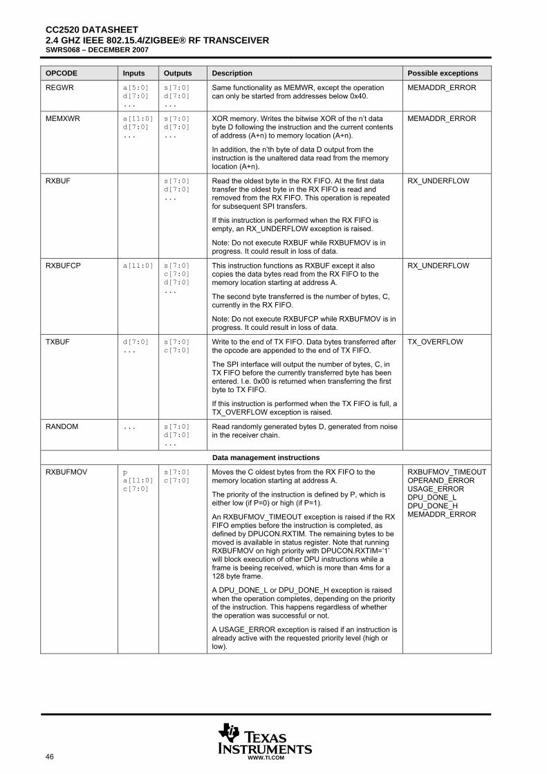
CC2520 DATASHEET 2.4 GHZ IEEE 802.15.4/ZIGBEE® RF TRANSCEIVER SWRS068 – DECEMBER 2007
46 WWW.TI.COM
OPCODE Inputs Outputs Description Possible exceptions
REGWR a[5:0] d[7:0] ...
s[7:0] d[7:0] ...
Same functionality as MEMWR, except the operation can only be started from addresses below 0x40.
MEMADDR_ERROR
MEMXWR a[11:0] d[7:0] ...
s[7:0] d[7:0] ...
XOR memory. Writes the bitwise XOR of the n’t data byte D following the instruction and the current contents of address (A+n) to memory location (A+n).
In addition, the n’th byte of data D output from the instruction is the unaltered data read from the memory location (A+n).
MEMADDR_ERROR
RXBUF s[7:0] d[7:0] ...
Read the oldest byte in the RX FIFO. At the first data transfer the oldest byte in the RX FIFO is read and removed from the RX FIFO. This operation is repeated for subsequent SPI transfers.
If this instruction is performed when the RX FIFO is empty, an RX_UNDERFLOW exception is raised.
Note: Do not execute RXBUF while RXBUFMOV is in progress. It could result in loss of data.
RX_UNDERFLOW
RXBUFCP a[11:0] s[7:0] c[7:0] d[7:0] ...
This instruction functions as RXBUF except it also copies the data bytes read from the RX FIFO to the memory location starting at address A.
The second byte transferred is the number of bytes, C, currently in the RX FIFO.
Note: Do not execute RXBUFCP while RXBUFMOV is in progress. It could result in loss of data.
RX_UNDERFLOW
TXBUF d[7:0] ...
s[7:0] c[7:0]
Write to the end of TX FIFO. Data bytes transferred after the opcode are appended to the end of TX FIFO.
The SPI interface will output the number of bytes, C, in TX FIFO before the currently transferred byte has been entered. I.e. 0x00 is returned when transferring the first byte to TX FIFO.
If this instruction is performed when the TX FIFO is full, a TX_OVERFLOW exception is raised.
TX_OVERFLOW
RANDOM ... s[7:0] d[7:0] ...
Read randomly generated bytes D, generated from noise in the receiver chain.
Data management instructions
RXBUFMOV p a[11:0] c[7:0]
s[7:0] c[7:0]
Moves the C oldest bytes from the RX FIFO to the memory location starting at address A.
The priority of the instruction is defined by P, which is either low (if P=0) or high (if P=1).
An RXBUFMOV_TIMEOUT exception is raised if the RX FIFO empties before the instruction is completed, as defined by DPUCON.RXTIM. The remaining bytes to be moved is available in status register. Note that running RXBUFMOV on high priority with DPUCON.RXTIM=’1’ will block execution of other DPU instructions while a frame is beeing received, which is more than 4ms for a 128 byte frame.
A DPU_DONE_L or DPU_DONE_H exception is raised when the operation completes, depending on the priority of the instruction. This happens regardless of whether the operation was successful or not.
A USAGE_ERROR exception is raised if an instruction is already active with the requested priority level (high or low).
RXBUFMOV_TIMEOUT OPERAND_ERROR USAGE_ERROR DPU_DONE_L DPU_DONE_H MEMADDR_ERROR
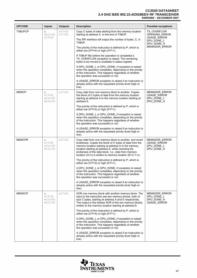
CC2520 DATASHEET2.4 GHZ IEEE 802.15.4/ZIGBEE® RF TRANSCEIVER
SWRS068 – DECEMBER 2007
WWW.TI.COM 47
OPCODE Inputs Outputs Description Possible exceptions
TXBUFCP p a[11:0] c[7:0]
s[7:0] c[7:0]
Copy C bytes of data starting from the memory location starting at address AT Tto the end of TXBUF.
The SPI interface will output the number of bytes, C, in TXBUF.
The priority of the instruction is defined by P, which is either low (if P=0) or high (if P=1).
If TXBUF fills before the operation is completed a TX_OVERFLOW exception is raised. The remaining bytes to be moved is available in status register.
A DPU_DONE_L or DPU_DONE_H exception is raised when the operation completes, depending on the priority of the instruction. This happens regardless of whether the operation was successful or not.
A USAGE_ERROR exception is raised if an instruction is already active with the requested priority level (high or low).
TX_OVERFLOW OPERAND_ERROR USAGE_ERROR DPU_DONE_L DPU_DONE_H MEMADDR_ERROR
MEMCP p c[7:0] a[11:0] e[11:0]
s[7:0] Copy data from one memory block to another. Copies the block of C bytes of data from the memory location starting at address A to the memory location starting at address E.
The priority of the instruction is defined by P, which is either low (if P=0) or high (if P=1).
A DPU_DONE_L or DPU_DONE_H exception is raised when the operation completes, depending on the priority of the instruction. This happens regardless of whether the operation was successful or not.
A USAGE_ERROR exception is raised if an instruction is already active with the requested priority level (high or low).
MEMADDR_ERROR USAGE_ERROR DPU_DONE_L DPU_DONE_H
MEMCPR p c[7:0] a[11:0] e[11:0]
s[7:0] Copy data from one memory block to another, and revert endianess. Copies the block of C bytes of data from the memory location starting at address A to the memory location starting at address E, while reverting the endianess of the data block. I.e., data from memory location (A+n) is written to memory location (E+C-1-n).
The priority of the instruction is defined by P, which is either low (if P=0) or high (if P=1).
A DPU_DONE_L or DPU_DONE_H exception is raised when the operation completes, depending on the priority of the instruction. This happens regardless of whether the operation was successful or not.
A USAGE_ERROR exception is raised if an instruction is already active with the requested priority level (high or low).
MEMADDR_ERROR USAGE_ERROR DPU_DONE_L DPU_DONE_H
MEMXCP p c[7:0] a[11:0] e[11:0]
s[7:0] XOR one memory block with another memory block. The input to the instruction are two memory blocks, both of size C bytes, starting at address A and E respectively. The output is the bitwise XOR of the two memory blocks, written to the memory location starting at address E.
The priority of the instruction is defined by P, which is either low (if P=0) or high (if P=1).
A DPU_DONE_L or DPU_DONE_H exception is raised when the operation completes, depending on the priority of the instruction. This happens regardless of whether the operation was successful or not.
A USAGE_ERROR exception is raised if an instruction is already active with the requested priority level (high or low).
MEMADDR_ERROR DPU_DONE_L DPU_DONE_H USAGE_ERROR
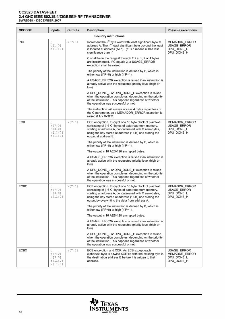
CC2520 DATASHEET 2.4 GHZ IEEE 802.15.4/ZIGBEE® RF TRANSCEIVER SWRS068 – DECEMBER 2007
48 WWW.TI.COM
OPCODE Inputs Outputs Description Possible exceptions
Security instructions
INC p c[1:0] a[11:0]
s[7:0] Increment the 2C byte word with least significant byte at address A. The nth least significant byte beyond the least is located at address (A+n). (n’ < n means n’ has less significance than n)
C shall be in the range 0 through 2, i.e. 1, 2 or 4 bytes are incremented. If C equals 3, a USAGE_ERROR exception shall be raised.
The priority of the instruction is defined by P, which is either low (if P=0) or high (if P=1).
A USAGE_ERROR exception is raised if an instruction is already active with the requested priority level (high or low).
A DPU_DONE_L or DPU_DONE_H exception is raised when the operation completes, depending on the priority of the instruction. This happens regardless of whether the operation was successful or not.
The instruction will always access 4 bytes regardless of the C parameter, so a MEMADDR_ERROR exception is raised if A > 0x3FC.
MEMADDR_ERROR USAGE_ERROR DPU_DONE_L DPU_DONE_H
ECB p k[7:0] c[3:0] a[11:0] e[11:0]
s[7:0] ECB encryption. Encrypt one 16 byte block of plaintext consisting of (16-C) bytes of data read from memory, starting at address A, concatenated with C zero-bytes, using the key stored at address (16⋅K) and storing the output at address E.
The priority of the instruction is defined by P, which is either low (if P=0) or high (if P=1).
The output is 16 AES-128 encrypted bytes.
A USAGE_ERROR exception is raised if an instruction is already active with the requested priority level (high or low).
A DPU_DONE_L or DPU_DONE_H exception is raised when the operation completes, depending on the priority of the instruction. This happens regardless of whether the operation was successful or not.
MEMADDR_ERROR USAGE_ERROR DPU_DONE_L DPU_DONE_H
ECBO p k[7:0] c[3:0] a[11:0]
s[7:0] ECB encryption. Encrypt one 16 byte block of plaintext consisting of (16-C) bytes of data read from memory, starting at address A, concatenated with C zero-bytes, using the key stored at address (16⋅K) and storing the output by overwriting the data from address A.
The priority of the instruction is defined by P, which is either low (if P=0) or high (if P=1).
The output is 16 AES-128 encrypted bytes.
A USAGE_ERROR exception is raised if an instruction is already active with the requested priority level (high or low).
A DPU_DONE_L or DPU_DONE_H exception is raised when the operation completes, depending on the priority of the instruction. This happens regardless of whether the operation was successful or not.
MEMADDR_ERROR USAGE_ERROR DPU_DONE_L DPU_DONE_H
ECBX p k[7:0] c[3:0] a[11:0] e[11:0]
s[7:0] ECB encryption and XOR. As ECB except each ciphertext byte is bitwise XOR’ed with the existing byte in the destination address E before it is written to that address.
USAGE_ERROR MEMADDR_ERROR DPU_DONE_L DPU_DONE_H
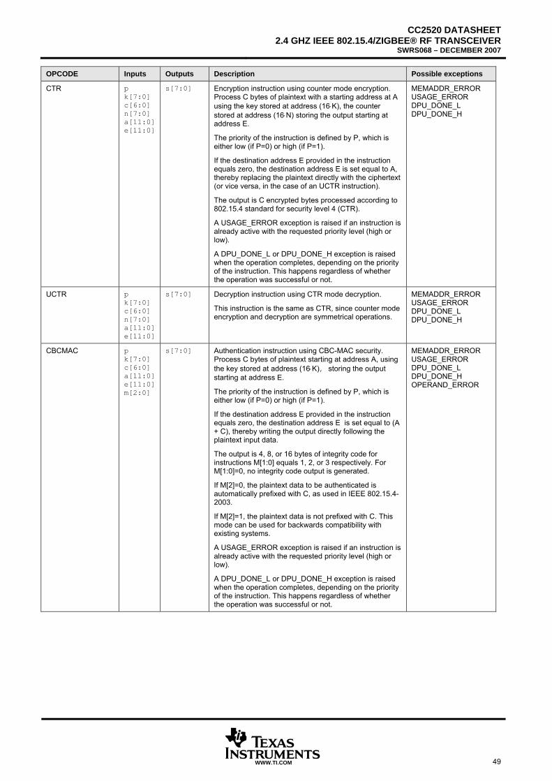
CC2520 DATASHEET2.4 GHZ IEEE 802.15.4/ZIGBEE® RF TRANSCEIVER
SWRS068 – DECEMBER 2007
WWW.TI.COM 49
OPCODE Inputs Outputs Description Possible exceptions
CTR p k[7:0] c[6:0] n[7:0] a[11:0] e[11:0]
s[7:0] Encryption instruction using counter mode encryption. Process C bytes of plaintext with a starting address at A using the key stored at address (16⋅K), the counter stored at address (16⋅N) storing the output starting at address E.
The priority of the instruction is defined by P, which is either low (if P=0) or high (if P=1).
If the destination address E provided in the instruction equals zero, the destination address E is set equal to A, thereby replacing the plaintext directly with the ciphertext (or vice versa, in the case of an UCTR instruction).
The output is C encrypted bytes processed according to 802.15.4 standard for security level 4 (CTR).
A USAGE_ERROR exception is raised if an instruction is already active with the requested priority level (high or low).
A DPU_DONE_L or DPU_DONE_H exception is raised when the operation completes, depending on the priority of the instruction. This happens regardless of whether the operation was successful or not.
MEMADDR_ERROR USAGE_ERROR DPU_DONE_L DPU_DONE_H
UCTR p k[7:0] c[6:0] n[7:0] a[11:0] e[11:0]
s[7:0] Decryption instruction using CTR mode decryption.
This instruction is the same as CTR, since counter mode encryption and decryption are symmetrical operations.
MEMADDR_ERROR USAGE_ERROR DPU_DONE_L DPU_DONE_H
CBCMAC p k[7:0] c[6:0] a[11:0] e[11:0] m[2:0]
s[7:0] Authentication instruction using CBC-MAC security. Process C bytes of plaintext starting at address A, using the key stored at address (16⋅K)T, Tstoring the output starting at address E.
The priority of the instruction is defined by P, which is either low (if P=0) or high (if P=1).
If the destination address E provided in the instruction equals zero, the destination address E is set equal to (A + C), thereby writing the output directly following the plaintext input data.
The output is 4, 8, or 16 bytes of integrity code for instructions M[1:0] equals 1, 2, or 3 respectively. For M[1:0]=0, no integrity code output is generated.
If M[2]=0, the plaintext data to be authenticated is automatically prefixed with C, as used in IEEE 802.15.4-2003.
If M[2]=1, the plaintext data is not prefixed with C. This mode can be used for backwards compatibility with existing systems.
A USAGE_ERROR exception is raised if an instruction is already active with the requested priority level (high or low).
A DPU_DONE_L or DPU_DONE_H exception is raised when the operation completes, depending on the priority of the instruction. This happens regardless of whether the operation was successful or not.
MEMADDR_ERROR USAGE_ERROR DPU_DONE_L DPU_DONE_H OPERAND_ERROR
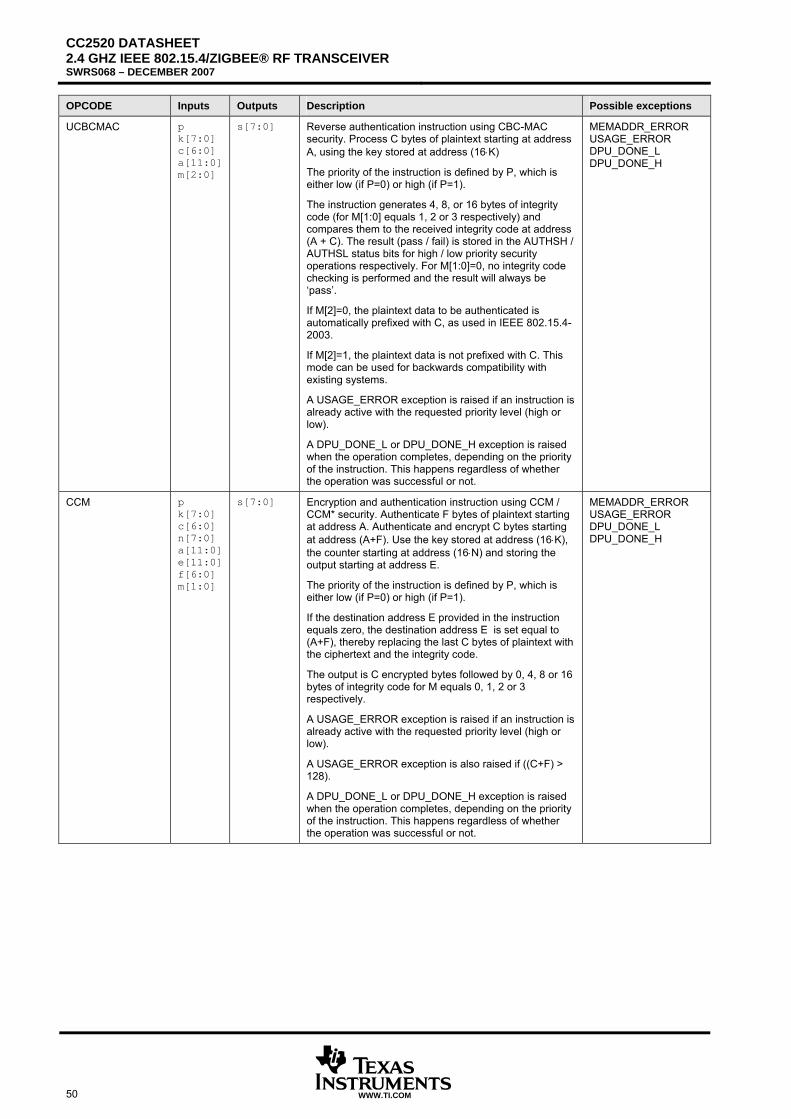
CC2520 DATASHEET 2.4 GHZ IEEE 802.15.4/ZIGBEE® RF TRANSCEIVER SWRS068 – DECEMBER 2007
50 WWW.TI.COM
OPCODE Inputs Outputs Description Possible exceptions
UCBCMAC p k[7:0] c[6:0] a[11:0] m[2:0]
s[7:0] Reverse authentication instruction using CBC-MAC security. Process C bytes of plaintext starting at address A, using the key stored at address (16⋅K)
The priority of the instruction is defined by P, which is either low (if P=0) or high (if P=1).
The instruction generates 4, 8, or 16 bytes of integrity code (for M[1:0] equals 1, 2 or 3 respectively) and compares them to the received integrity code at address (A + C). The result (pass / fail) is stored in the AUTHSH / AUTHSL status bits for high / low priority security operations respectively. For M[1:0]=0, no integrity code checking is performed and the result will always be ‘pass’.
If M[2]=0, the plaintext data to be authenticated is automatically prefixed with C, as used in IEEE 802.15.4-2003.
If M[2]=1, the plaintext data is not prefixed with C. This mode can be used for backwards compatibility with existing systems.
A USAGE_ERROR exception is raised if an instruction is already active with the requested priority level (high or low).
A DPU_DONE_L or DPU_DONE_H exception is raised when the operation completes, depending on the priority of the instruction. This happens regardless of whether the operation was successful or not.
MEMADDR_ERROR USAGE_ERROR DPU_DONE_L DPU_DONE_H
CCM p k[7:0] c[6:0] n[7:0] a[11:0] e[11:0] f[6:0] m[1:0]
s[7:0] Encryption and authentication instruction using CCM / CCM* security. Authenticate F bytes of plaintext starting at address A. Authenticate and encrypt C bytes starting at address (A+F). Use the key stored at address (16⋅K), the counter starting at address (16⋅N) and storing the output starting at address E.
The priority of the instruction is defined by P, which is either low (if P=0) or high (if P=1).
If the destination address E provided in the instruction equals zero, the destination address E is set equal to (A+F), thereby replacing the last C bytes of plaintext with the ciphertext and the integrity code.
The output is C encrypted bytes followed by 0, 4, 8 or 16 bytes of integrity code for M equals 0, 1, 2 or 3 respectively.
A USAGE_ERROR exception is raised if an instruction is already active with the requested priority level (high or low).
A USAGE_ERROR exception is also raised if ((C+F) > 128).
A DPU_DONE_L or DPU_DONE_H exception is raised when the operation completes, depending on the priority of the instruction. This happens regardless of whether the operation was successful or not.
MEMADDR_ERROR USAGE_ERROR DPU_DONE_L DPU_DONE_H
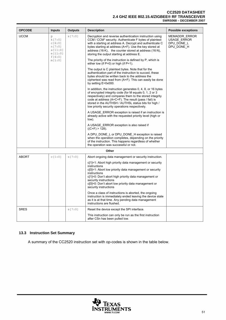
CC2520 DATASHEET2.4 GHZ IEEE 802.15.4/ZIGBEE® RF TRANSCEIVER
SWRS068 – DECEMBER 2007
WWW.TI.COM 51
OPCODE Inputs Outputs Description Possible exceptions
UCCM p k[7:0] c[6:0] n[7:0] a[11:0] e[11:0] f[6:0] m[1:0]
s[7:0] Decryption and reverse authentication instruction using CCM / CCM* security. Authenticate F bytes of plaintext with a starting at address A. Decrypt and authenticate C bytes starting at address (A+F). Use the key stored at address (16⋅K)T, Tthe counter stored at address (16⋅N), storing the output starting at address E.
The priority of the instruction is defined by P, which is either low (if P=0) or high (if P=1).
The output is C plaintext bytes. Note that for the authentication part of the instruction to succed, these bytes should be written back to the address the ciphertext was read from (A+F). This can easily be done by setting E=0x000.
In addition, the instruction generates 0, 4, 8, or 16 bytes of encrypted integrity code (for M equals 0, 1, 2 or 3 respectively) and compares them to the stored integrity code at address (A+C+F). The result (pass / fail) is stored in the AUTHSH / AUTHSL status bits for high / low priority security operations respectively.
A USAGE_ERROR exception is raised if an instruction is already active with the requested priority level (high or low).
A USAGE_ERROR exception is also raised if ((C+F) > 128).
A DPU_DONE_L or DPU_DONE_H exception is raised when the operation completes, depending on the priority of the instruction. This happens regardless of whether the operation was successful or not.
MEMADDR_ERROR USAGE_ERROR DPU_DONE_L DPU_DONE_H
Other
ABORT c[1:0] s[7:0] Abort ongoing data management or security instruction.
c[1]=1: Abort high priority data management or security instructions c[0]=1: Abort low priority data management or security instructions c[1]=0: Don’t abort high priority data management or security instructions c[0]=0: Don’t abort low priority data management or security instructions
Once a class of instructions is aborted, the ongoing instruction is immediately ended leaving the device state as it is at that time. Any pending data management instructions are flushed.
SRES s[7:0] Reset the device except the SPI interface.
This instruction can only be run as the first instruction after CSn has been pulled low.
13.3 Instruction Set Summary
A summary of the CC2520 instruction set with op-codes is shown in the table below.
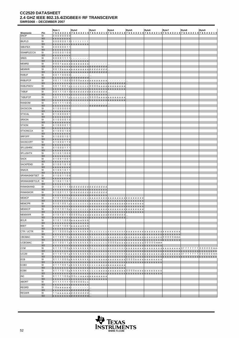
CC2520 DATASHEET 2.4 GHZ IEEE 802.15.4/ZIGBEE® RF TRANSCEIVER SWRS068 – DECEMBER 2007
52 WWW.TI.COM
Byte 1 Byte2 Byte3 Byte4 Byte5 Byte6 Byte7 Byte8 Byte9Mnemonic Pin 7 6 5 4 3 2 1 0 7 6 5 4 3 2 1 0 7 6 5 4 3 2 1 0 7 6 5 4 3 2 1 0 7 6 5 4 3 2 1 0 7 6 5 4 3 2 1 0 7 6 5 4 3 2 1 0 7 6 5 4 3 2 1 0 7 6 5 4 3 2 1 0SNOP SI 0 0 0 0 0 0 0 0
SO s s s s s s s sIBUFLD SI 0 0 0 0 0 0 1 0 i i i i i i i i
SO s s s s s s s s s s s s s s s sSIBUFEX SI 0 0 0 0 0 0 1 1
SO s s s s s s s sSSAMPLECCA SI 0 0 0 0 0 1 0 0
SO s s s s s s s sSRES SI 0 0 0 0 1 1 1 1 - - - - - - - -
SO s s s s s s s s s s s s s s s sMEMRD SI 0 0 0 1 a a a a a a a a a a a a - - - - - - - - ...
SO s s s s s s s s s s s s s s s s d d d d d d d d ...MEMWR SI 0 0 1 0 a a a a a a a a a a a a d d d d d d d d ...
SO s s s s s s s s s s s s s s s s d d d d d d d d ...RXBUF SI 0 0 1 1 0 0 0 0 - - - - - - - - ...
SO s s s s s s s s d d d d d d d d ...RXBUFCP SI 0 0 1 1 1 0 0 0 0 0 0 0 a a a a a a a a a a a a - - - - - - - - ...
SO s s s s s s s s c c c c c c c c s s s s s s s s d d d d d d d d ...RXBUFMOV SI 0 0 1 1 0 0 1 p c c c c c c c c 0 0 0 0 a a a a a a a a a a a a
SO s s s s s s s s c c c c c c c c s s s s s s s s s s s s s s s sTXBUF SI 0 0 1 1 1 0 1 0 d d d d d d d d d d d d d d d d ...
SO s s s s s s s s c c c c c c c c s s s s s s s s ...TXBUFCP SI 0 0 1 1 1 1 1 p c c c c c c c c 0 0 0 0 a a a a a a a a a a a a
SO s s s s s s s s c c c c c c c c s s s s s s s s s s s s s s s sRANDOM SI 0 0 1 1 1 1 0 0 - - - - - - - - - - - - - - - - ...
SO s s s s s s s s - - - - - - - - d d d d d d d d ...SXOSCON SI 0 1 0 0 0 0 0 0
SO s s s s s s s sSTXCAL SI 0 1 0 0 0 0 0 1
SO s s s s s s s sSRXON SI 0 1 0 0 0 0 1 0
SO s s s s s s s sSTXON SI 0 1 0 0 0 0 1 1
SO s s s s s s s sSTXONCCA SI 0 1 0 0 0 1 0 0
SO s s s s s s s sSRFOFF SI 0 1 0 0 0 1 0 1
SO s s s s s s s sSXOSCOFF SI 0 1 0 0 0 1 1 0
SO s s s s s s s sSFLUSHRX SI 0 1 0 0 0 1 1 1
SO s s s s s s s sSFLUSHTX SI 0 1 0 0 1 0 0 0
SO s s s s s s s sSACK SI 0 1 0 0 1 0 0 1
SO s s s s s s s sSACKPEND SI 0 1 0 0 1 0 1 0
SO s s s s s s s sSNACK SI 0 1 0 0 1 0 1 1
SO s s s s s s s sSRXMASKBITSET SI 0 1 0 0 1 1 0 0
SO s s s s s s s sSRXMASKBITCLR SI 0 1 0 0 1 1 0 1
SO s s s s s s s sRXMASKAND SI 0 1 0 0 1 1 1 0 d d d d d d d d d d d d d d d d
SO s s s s s s s s s s s s s s s s s s s s s s s sRXMASKOR SI 0 1 0 0 1 1 1 1 d d d d d d d d d d d d d d d d
SO s s s s s s s s s s s s s s s s s s s s s s s sMEMCP SI 0 1 0 1 0 0 0 p c c c c c c c c a a a a e e e e a a a a a a a a e e e e e e e e
SO s s s s s s s s s s s s s s s s s s s s s s s s s s s s s s s s s s s s s s s sMEMCPR SI 0 1 0 1 0 0 1 p c c c c c c c c a a a a e e e e a a a a a a a a e e e e e e e e
SO s s s s s s s s s s s s s s s s s s s s s s s s s s s s s s s s s s s s s s s sMEMXCP SI 0 1 0 1 0 1 0 p c c c c c c c c a a a a e e e e a a a a a a a a e e e e e e e e
SO s s s s s s s s s s s s s s s s s s s s s s s s s s s s s s s s s s s s s s s sMEMXWR SI 0 1 0 1 0 1 1 0 0 0 0 0 a a a a a a a a a a a a d d d d d d d d ...
SO s s s s s s s s s s s s s s s s s s s s s s s s d d d d d d d d ...BCLR SI 0 1 0 1 1 0 0 0 a a a a a b b b
SO s s s s s s s s s s s s s s s sBSET SI 0 1 0 1 1 0 0 1 a a a a a b b b
SO s s s s s s s s s s s s s s s sCTR / UCTR SI 0 1 1 0 0 0 0 p k k k k k k k k 0 c c c c c c c n n n n n n n n a a a a e e e e a a a a a a a a e e e e e e e e
SO s s s s s s s s s s s s s s s s s s s s s s s s s s s s s s s s s s s s s s s s s s s s s s s s s s s s s s s sCBCMAC SI 0 1 1 0 0 1 0 p k k k k k k k k 0 c c c c c c c a a a a e e e e a a a a a a a a e e e e e e e e 0 0 0 0 0 m m m
SO s s s s s s s s s s s s s s s s s s s s s s s s s s s s s s s s s s s s s s s s s s s s s s s s s s s s s s s sUCBCMAC SI 0 1 1 0 0 1 1 p k k k k k k k k 0 c c c c c c c 0 0 0 0 a a a a a a a a a a a a 0 0 0 0 0 m m m
SO s s s s s s s s s s s s s s s s s s s s s s s s s s s s s s s s s s s s s s s s s s s s s s s sCCM SI 0 1 1 0 1 0 0 p k k k k k k k k 0 c c c c c c c n n n n n n n n a a a a e e e e a a a a a a a a e e e e e e e e 0 f f f f f f f 0 0 0 0 0 0 m m
SO s s s s s s s s s s s s s s s s s s s s s s s s s s s s s s s s s s s s s s s s s s s s s s s s s s s s s s s s s s s s s s s s s s s s s s s sUCCM SI 0 1 1 0 1 0 1 p k k k k k k k k 0 c c c c c c c n n n n n n n n a a a a e e e e a a a a a a a a e e e e e e e e 0 f f f f f f f 0 0 0 0 0 0 m m
SO s s s s s s s s s s s s s s s s s s s s s s s s s s s s s s s s s s s s s s s s s s s s s s s s s s s s s s s s s s s s s s s s s s s s s s s sECB SI 0 1 1 1 0 0 0 p k k k k k k k k c c c c a a a a a a a a a a a a 0 0 0 0 e e e e e e e e e e e e
SO s s s s s s s s s s s s s s s s s s s s s s s s s s s s s s s s s s s s s s s s s s s s s s s sECBO SI 0 1 1 1 0 0 1 p k k k k k k k k c c c c a a a a a a a a a a a a
SO s s s s s s s s s s s s s s s s s s s s s s s s s s s s s s s sECBX SI 0 1 1 1 0 1 0 p k k k k k k k k c c c c a a a a a a a a a a a a 0 0 0 0 e e e e e e e e e e e e
SO s s s s s s s s s s s s s s s s s s s s s s s s s s s s s s s s s s s s s s s s s s s s s s s sINC SI 0 1 1 1 1 0 0 p 0 0 c c a a a a a a a a a a a a
SO s s s s s s s s s s s s s s s s s s s s s s s sABORT SI 0 1 1 1 1 1 1 1 0 0 0 0 0 0 c c
SO s s s s s s s s s s s s s s s sREGRD SI 1 0 a a a a a a - - - - - - - - ...
SO s s s s s s s s d d d d d d d d ...REGWR SI 1 1 a a a a a a d d d d d d d d ...
SO s s s s s s s s d d d d d d d d ...
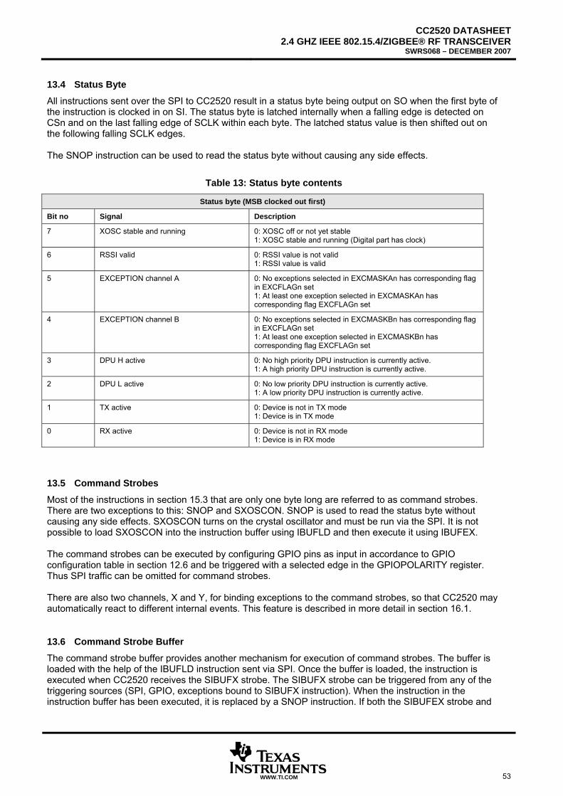
CC2520 DATASHEET2.4 GHZ IEEE 802.15.4/ZIGBEE® RF TRANSCEIVER
SWRS068 – DECEMBER 2007
WWW.TI.COM 53
13.4 Status Byte
All instructions sent over the SPI to CC2520 result in a status byte being output on SO when the first byte of the instruction is clocked in on SI. The status byte is latched internally when a falling edge is detected on CSn and on the last falling edge of SCLK within each byte. The latched status value is then shifted out on the following falling SCLK edges. The SNOP instruction can be used to read the status byte without causing any side effects.
Table 13: Status byte contents
Status byte (MSB clocked out first)
Bit no Signal Description
7 XOSC stable and running 0: XOSC off or not yet stable 1: XOSC stable and running (Digital part has clock)
6 RSSI valid 0: RSSI value is not valid 1: RSSI value is valid
5 EXCEPTION channel A 0: No exceptions selected in EXCMASKAn has corresponding flag in EXCFLAGn set 1: At least one exception selected in EXCMASKAn has corresponding flag EXCFLAGn set
4 EXCEPTION channel B 0: No exceptions selected in EXCMASKBn has corresponding flag in EXCFLAGn set 1: At least one exception selected in EXCMASKBn has corresponding flag EXCFLAGn set
3 DPU H active 0: No high priority DPU instruction is currently active. 1: A high priority DPU instruction is currently active.
2 DPU L active 0: No low priority DPU instruction is currently active. 1: A low priority DPU instruction is currently active.
1 TX active 0: Device is not in TX mode 1: Device is in TX mode
0 RX active 0: Device is not in RX mode 1: Device is in RX mode
13.5 Command Strobes
Most of the instructions in section 15.3 that are only one byte long are referred to as command strobes. There are two exceptions to this: SNOP and SXOSCON. SNOP is used to read the status byte without causing any side effects. SXOSCON turns on the crystal oscillator and must be run via the SPI. It is not possible to load SXOSCON into the instruction buffer using IBUFLD and then execute it using IBUFEX. The command strobes can be executed by configuring GPIO pins as input in accordance to GPIO configuration table in section 12.6 and be triggered with a selected edge in the GPIOPOLARITY register. Thus SPI traffic can be omitted for command strobes. There are also two channels, X and Y, for binding exceptions to the command strobes, so that CC2520 may automatically react to different internal events. This feature is described in more detail in section 16.1.
13.6 Command Strobe Buffer
The command strobe buffer provides another mechanism for execution of command strobes. The buffer is loaded with the help of the IBUFLD instruction sent via SPI. Once the buffer is loaded, the instruction is executed when CC2520 receives the SIBUFX strobe. The SIBUFX strobe can be triggered from any of the triggering sources (SPI, GPIO, exceptions bound to SIBUFX instruction). When the instruction in the instruction buffer has been executed, it is replaced by a SNOP instruction. If both the SIBUFEX strobe and

CC2520 DATASHEET 2.4 GHZ IEEE 802.15.4/ZIGBEE® RF TRANSCEIVER SWRS068 – DECEMBER 2007
54 WWW.TI.COM
the IBUFLD instruction are received at the same time, the old command strobe is executed. The new strobe that the user tried to write to the buffer is lost and will never be executed.
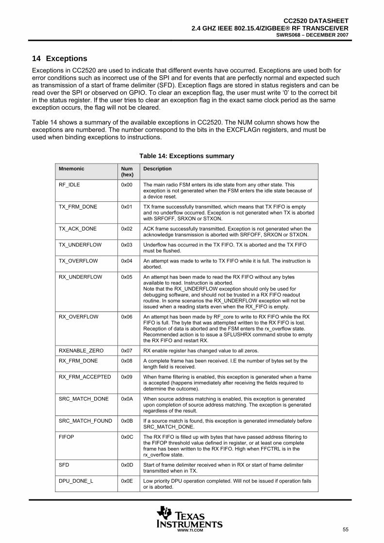
CC2520 DATASHEET2.4 GHZ IEEE 802.15.4/ZIGBEE® RF TRANSCEIVER
SWRS068 – DECEMBER 2007
WWW.TI.COM 55
14 Exceptions Exceptions in CC2520 are used to indicate that different events have occurred. Exceptions are used both for error conditions such as incorrect use of the SPI and for events that are perfectly normal and expected such as transmission of a start of frame delimiter (SFD). Exception flags are stored in status registers and can be read over the SPI or observed on GPIO. To clear an exception flag, the user must write ‘0’ to the correct bit in the status register. If the user tries to clear an exception flag in the exact same clock period as the same exception occurs, the flag will not be cleared. Table 14 shows a summary of the available exceptions in CC2520. The NUM column shows how the exceptions are numbered. The number correspond to the bits in the EXCFLAGn registers, and must be used when binding exceptions to instructions.
Table 14: Exceptions summary
Mnemonic Num (hex)
Description
RF_IDLE 0x00 The main radio FSM enters its idle state from any other state. This exception is not generated when the FSM enters the idle state because of a device reset.
TX_FRM_DONE 0x01 TX frame successfully transmitted, which means that TX FIFO is empty and no underflow occurred. Exception is not generated when TX is aborted with SRFOFF, SRXON or STXON.
TX_ACK_DONE 0x02 ACK frame successfully transmitted. Exception is not generated when the acknowledge transmission is aborted with SRFOFF, SRXON or STXON.
TX_UNDERFLOW 0x03 Underflow has occurred in the TX FIFO. TX is aborted and the TX FIFO must be flushed.
TX_OVERFLOW 0x04 An attempt was made to write to TX FIFO while it is full. The instruction is aborted.
RX_UNDERFLOW 0x05 An attempt has been made to read the RX FIFO without any bytes available to read. Instruction is aborted. Note that the RX_UNDERFLOW exception should only be used for debugging software, and should not be trusted in a RX FIFO readout routine. In some scenarios the RX_UNDERFLOW exception will not be issued when a reading starts even when the RX_FIFO is empty.
RX_OVERFLOW 0x06 An attempt has been made by RF_core to write to RX FIFO while the RX FIFO is full. The byte that was attempted written to the RX FIFO is lost. Reception of data is aborted and the FSM enters the rx_overflow state. Recommended action is to issue a SFLUSHRX command strobe to empty the RX FIFO and restart RX.
RXENABLE_ZERO 0x07 RX enable register has changed value to all zeros.
RX_FRM_DONE 0x08 A complete frame has been received. I.E the number of bytes set by the length field is received.
RX_FRM_ACCEPTED 0x09 When frame filtering is enabled, this exception is generated when a frame is accepted (happens immediately after receiving the fields required to determine the outcome).
SRC_MATCH_DONE 0x0A When source address matching is enabled, this exception is generated upon completion of source address matching. The exception is generated regardless of the result.
SRC_MATCH_FOUND 0x0B If a source match is found, this exception is generated immediately before SRC_MATCH_DONE.
FIFOP 0x0C The RX FIFO is filled up with bytes that have passed address filtering to the FIFOP threshold value defined in register, or at least one complete frame has been written to the RX FIFO. High when FFCTRL is in the rx_overflow state.
SFD 0x0D Start of frame delimiter received when in RX or start of frame delimiter transmitted when in TX.
DPU_DONE_L 0x0E Low priority DPU operation completed. Will not be issued if operation fails or is aborted.
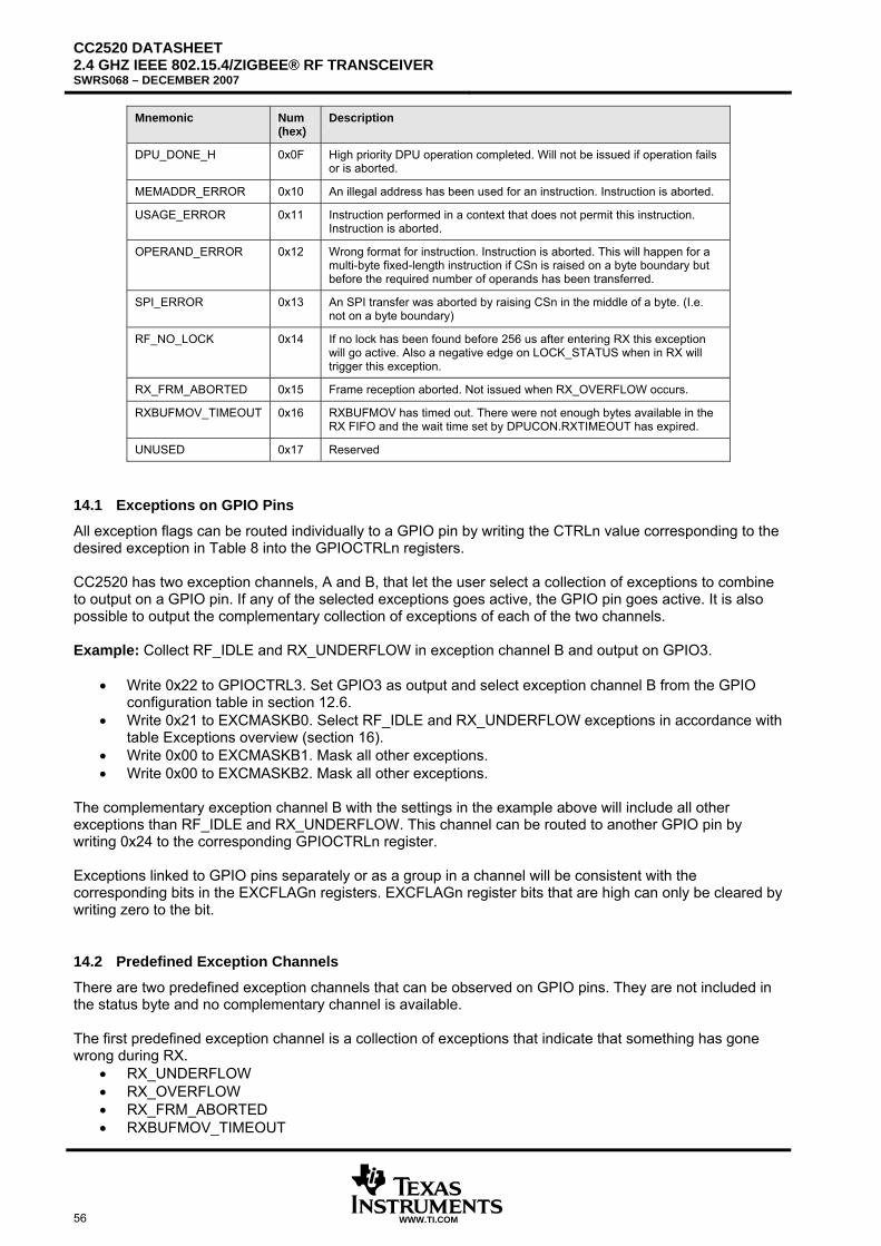
CC2520 DATASHEET 2.4 GHZ IEEE 802.15.4/ZIGBEE® RF TRANSCEIVER SWRS068 – DECEMBER 2007
56 WWW.TI.COM
Mnemonic Num (hex)
Description
DPU_DONE_H 0x0F High priority DPU operation completed. Will not be issued if operation fails or is aborted.
MEMADDR_ERROR 0x10 An illegal address has been used for an instruction. Instruction is aborted.
USAGE_ERROR 0x11 Instruction performed in a context that does not permit this instruction. Instruction is aborted.
OPERAND_ERROR 0x12 Wrong format for instruction. Instruction is aborted. This will happen for a multi-byte fixed-length instruction if CSn is raised on a byte boundary but before the required number of operands has been transferred.
SPI_ERROR 0x13 An SPI transfer was aborted by raising CSn in the middle of a byte. (I.e. not on a byte boundary)
RF_NO_LOCK 0x14 If no lock has been found before 256 us after entering RX this exception will go active. Also a negative edge on LOCK_STATUS when in RX will trigger this exception.
RX_FRM_ABORTED 0x15 Frame reception aborted. Not issued when RX_OVERFLOW occurs.
RXBUFMOV_TIMEOUT 0x16 RXBUFMOV has timed out. There were not enough bytes available in the RX FIFO and the wait time set by DPUCON.RXTIMEOUT has expired.
UNUSED 0x17 Reserved
14.1 Exceptions on GPIO Pins
All exception flags can be routed individually to a GPIO pin by writing the CTRLn value corresponding to the desired exception in Table 8 into the GPIOCTRLn registers. CC2520 has two exception channels, A and B, that let the user select a collection of exceptions to combine to output on a GPIO pin. If any of the selected exceptions goes active, the GPIO pin goes active. It is also possible to output the complementary collection of exceptions of each of the two channels. Example: Collect RF_IDLE and RX_UNDERFLOW in exception channel B and output on GPIO3.
• Write 0x22 to GPIOCTRL3. Set GPIO3 as output and select exception channel B from the GPIO configuration table in section 12.6.
• Write 0x21 to EXCMASKB0. Select RF_IDLE and RX_UNDERFLOW exceptions in accordance with table Exceptions overview (section 16).
• Write 0x00 to EXCMASKB1. Mask all other exceptions. • Write 0x00 to EXCMASKB2. Mask all other exceptions.
The complementary exception channel B with the settings in the example above will include all other exceptions than RF_IDLE and RX_UNDERFLOW. This channel can be routed to another GPIO pin by writing 0x24 to the corresponding GPIOCTRLn register. Exceptions linked to GPIO pins separately or as a group in a channel will be consistent with the corresponding bits in the EXCFLAGn registers. EXCFLAGn register bits that are high can only be cleared by writing zero to the bit.
14.2 Predefined Exception Channels
There are two predefined exception channels that can be observed on GPIO pins. They are not included in the status byte and no complementary channel is available. The first predefined exception channel is a collection of exceptions that indicate that something has gone wrong during RX.
• RX_UNDERFLOW • RX_OVERFLOW • RX_FRM_ABORTED • RXBUFMOV_TIMEOUT
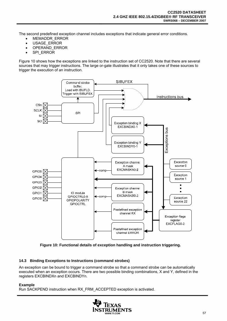
CC2520 DATASHEET2.4 GHZ IEEE 802.15.4/ZIGBEE® RF TRANSCEIVER
SWRS068 – DECEMBER 2007
WWW.TI.COM 57
The second predefined exception channel includes exceptions that indicate general error conditions.
• MEMADDR_ERROR • USAGE_ERROR • OPERAND_ERROR • SPI_ERROR
Figure 10 shows how the exceptions are linked to the instruction set of CC2520. Note that there are several sources that may trigger instructions. The large or-gate illustrates that it only takes one of these sources to trigger the execution of an instruction.
Exce
ptio
ns b
us
Figure 10: Functional details of exception handling and instruction triggering.
14.3 Binding Exceptions to Instructions (command strobes)
An exception can be bound to trigger a command strobe so that a command strobe can be automatically executed when an exception occurs. There are two possible binding combinations, X and Y, defined in the registers EXCBINDXn and EXCBINDYn. Example Run SACKPEND instruction when RX_FRM_ACCEPTED exception is activated.

CC2520 DATASHEET 2.4 GHZ IEEE 802.15.4/ZIGBEE® RF TRANSCEIVER SWRS068 – DECEMBER 2007
58 WWW.TI.COM
1. Write 0x06 to EXCBINDX0. This will select SACKPEND as the bound instruction from Table 8: GPIO
configuration. 2. Write 0x89 to EXCBINDX1. Enables X-binding and selects RX_FRM_ACCEPTED as the bound
exception from Table 14: Exceptions summary. Note Be aware of the offset in numbering in the tables Exceptions summary (section 16) and GPIO configuration (section 12.6) for exceptions. It is for example possible to route the exception RF_IDLE to a GPIO pin in the GPIOCTRLn.CTRLn register bit when the pin is set as output. In this case, the exception RF_IDLE has the numbering 0x01 in accordance to Table 9: GPIO configuration When RF_IDLE is to be bound with an instruction the numbering to be used in EXCBINDX/Y1 is 0x00 in accordance to Table 14: Exceptions summary.
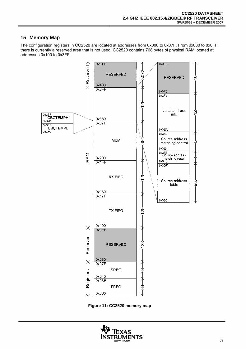
CC2520 DATASHEET2.4 GHZ IEEE 802.15.4/ZIGBEE® RF TRANSCEIVER
SWRS068 – DECEMBER 2007
WWW.TI.COM 59
15 Memory Map The configuration registers in CC2520 are located at addresses from 0x000 to 0x07F. From 0x080 to 0x0FF there is currently a reserved area that is not used. CC2520 contains 768 bytes of physical RAM located at addresses 0x100 to 0x3FF.
Figure 11: CC2520 memory map
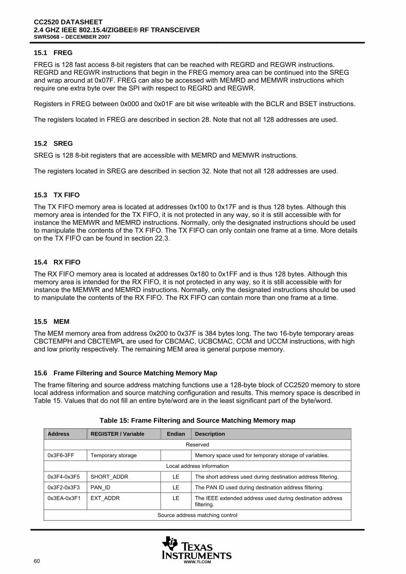
CC2520 DATASHEET 2.4 GHZ IEEE 802.15.4/ZIGBEE® RF TRANSCEIVER SWRS068 – DECEMBER 2007
60 WWW.TI.COM
15.1 FREG
FREG is 128 fast access 8-bit registers that can be reached with REGRD and REGWR instructions. REGRD and REGWR instructions that begin in the FREG memory area can be continued into the SREG and wrap around at 0x07F. FREG can also be accessed with MEMRD and MEMWR instructions which require one extra byte over the SPI with respect to REGRD and REGWR. Registers in FREG between 0x000 and 0x01F are bit wise writeable with the BCLR and BSET instructions. The registers located in FREG are described in section 28. Note that not all 128 addresses are used.
15.2 SREG
SREG is 128 8-bit registers that are accessible with MEMRD and MEMWR instructions. The registers located in SREG are described in section 32. Note that not all 128 addresses are used.
15.3 TX FIFO
The TX FIFO memory area is located at addresses 0x100 to 0x17F and is thus 128 bytes. Although this memory area is intended for the TX FIFO, it is not protected in any way, so it is still accessible with for instance the MEMWR and MEMRD instructions. Normally, only the designated instructions should be used to manipulate the contents of the TX FIFO. The TX FIFO can only contain one frame at a time. More details on the TX FIFO can be found in section 22.3.
15.4 RX FIFO
The RX FIFO memory area is located at addresses 0x180 to 0x1FF and is thus 128 bytes. Although this memory area is intended for the RX FIFO, it is not protected in any way, so it is still accessible with for instance the MEMWR and MEMRD instructions. Normally, only the designated instructions should be used to manipulate the contents of the RX FIFO. The RX FIFO can contain more than one frame at a time.
15.5 MEM
The MEM memory area from address 0x200 to 0x37F is 384 bytes long. The two 16-byte temporary areas CBCTEMPH and CBCTEMPL are used for CBCMAC, UCBCMAC, CCM and UCCM instructions, with high and low priority respectively. The remaining MEM area is general purpose memory.
15.6 Frame Filtering and Source Matching Memory Map
The frame filtering and source address matching functions use a 128-byte block of CC2520 memory to store local address information and source matching configuration and results. This memory space is described in Table 15. Values that do not fill an entire byte/word are in the least significant part of the byte/word.
Table 15: Frame Filtering and Source Matching Memory map
Address REGISTER / Variable Endian Description
Reserved
0x3F6-3FF Temporary storage Memory space used for temporary storage of variables.
Local address information
0x3F4-0x3F5 SHORT_ADDR LE The short address used during destination address filtering.
0x3F2-0x3F3 PAN_ID LE The PAN ID used during destination address filtering.
0x3EA-0x3F1 EXT_ADDR LE The IEEE extended address used during destination address filtering.
Source address matching control
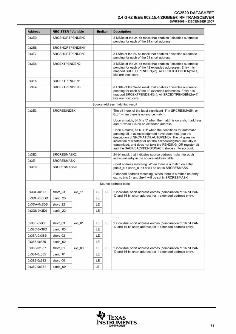
CC2520 DATASHEET2.4 GHZ IEEE 802.15.4/ZIGBEE® RF TRANSCEIVER
SWRS068 – DECEMBER 2007
WWW.TI.COM 61
Address REGISTER / Variable Endian Description
0x3E9 SRCSHORTPENDEN2 8 MSBs of the 24-bit mask that enables / disables automatic pending for each of the 24 short address.
0x3E8 SRCSHORTPENDEN1
0x3E7 SRCSHORTPENDEN0 8 LSBs of the 24-bit mask that enables / disables automatic pending for each of the 24 short address.
0x3E6 SRCEXTPENDEN2 8 MSBs of the 24-bit mask that enables / disables automatic pending for each of the 12 extended addresses. Entry n is mapped SRCEXTPENDEN[2n]. All SRCEXTPENDEN[2n+1] bits are don't care.
0x3E5 SRCEXTPENDEN1
0x3E4 SRCEXTPENDEN0 8 LSBs of the 24-bit mask that enables / disables automatic pending for each of the 12 extended addresses. Entry n is mapped SRCEXTPENDEN[2n]. All SRCEXTPENDEN[2n+1] bits are don't care.
Source address matching result
0x3E3 SRCRESINDEX The bit index of the least significant '1' in SRCRESMASK, or 0x3F when there is no source match.
Upon a match, bit 5 is '0' when the match is on a short address and '1' when it is on an extended address.
Upon a match, bit 6 is '1' when the conditions for automatic pending bit in acknowledgment have been met (see the description of SRCMATCH.AUTOPEND). The bit gives no indication of whether or not the acknowledgment actually is transmitted, and does not take the PENDING_OR register bit and the SACK/SACKPEND/SNACK strobes into account.
0x3E2 SRCRESMASK2
0x3E1 SRCRESMASK1
0x3E0 SRCRESMASK0
24-bit mask that indicates source address match for each individual entry in the source address table.
Short address matching: When there is a match on entry panid_n + short_n, bit n will be set in SRCRESMASK.
Extended address matching: When there is a match on entry ext_n, bits 2n and 2n+1 will be set in SRCRESMASK.
Source address table
0x3DE-0x3DF short_23 LE
0x3DC-0x3DD panid_23 LE
0x3DA-0x3DB short_22 LE
0x3D8-0x3D9 panid_22
ext_11
LE
LE 2 individual short address entries (combination of 16 bit PAN ID and 16 bit short address) or 1 extended address entry.
- - - - -
0x38E-0x38F short_03 LE
0x38C-0x38D panid_03 LE
0x38A-0x38B short_02 LE
0x388-0x389 panid_02
ext_01
LE
LE 2 individual short address entries (combination of 16 bit PAN ID and 16 bit short address) or 1 extended address entry.
0x386-0x387 short_01 LE
0x384-0x385 panid_01 LE
0x382-0x383 short_00 LE
0x380-0x381 panid_00
ext_00
LE
LE 2 individual short address entries (combination of 16 bit PAN ID and 16 bit short address) or 1 extended address entry.

CC2520 DATASHEET 2.4 GHZ IEEE 802.15.4/ZIGBEE® RF TRANSCEIVER SWRS068 – DECEMBER 2007
62 WWW.TI.COM
16 Frequency and Channel Programming The carrier frequency is set by programming the 7 bit frequency word located in FREQCTRL.FREQ[6:0]. CC2520 supports carrier frequencies in the range 2394MHz to 2507MHz. The carrier frequency FC in MHz is given by FC = (2394 + FREQCTRL.FREQ[6:0]) MHz, and is programmable in 1 MHz steps. IEEE 802.15.4-2006 specifies 16 channels within the 2.4 GHz band. They are numbered 11 through 26 and are 5 MHz apart. The RF frequency of channel k is given by [2].
[ ] [ ]26,11)11(52405 ∈−+= kMHzkFc For operation in channel k, the FREQCTRL.FREQ register should therefore be set to FREQCTRL.FREQ = 11 + 5 (k-11)
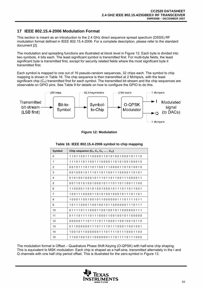
CC2520 DATASHEET2.4 GHZ IEEE 802.15.4/ZIGBEE® RF TRANSCEIVER
SWRS068 – DECEMBER 2007
WWW.TI.COM 63
17 IEEE 802.15.4-2006 Modulation Format This section is meant as an introduction to the 2.4 GHz direct sequence spread spectrum (DSSS) RF modulation format defined in IEEE 802.15.4-2006. For a complete description, please refer to the standard document [2]. The modulation and spreading functions are illustrated at block level in Figure 12. Each byte is divided into two symbols, 4 bits each. The least significant symbol is transmitted first. For multi-byte fields, the least significant byte is transmitted first, except for security related fields where the most significant byte it transmitted first. Each symbol is mapped to one out of 16 pseudo-random sequences, 32 chips each. The symbol to chip mapping is shown in Table 16. The chip sequence is then transmitted at 2 Mchips/s, with the least significant chip (C0) transmitted first for each symbol. The transmitted bit stream and the chip sequences are observable on GPIO pins. See Table 9 for details on how to configure the GPIO to do this.
Figure 12: Modulation
Table 16: IEEE 802.15.4-2006 symbol to chip mapping
Symbol Chip sequence (C0, C1, C2, … , C31)
0 1 1 0 1 1 0 0 1 1 1 0 0 0 0 1 1 0 1 0 1 0 0 1 0 0 0 1 0 1 1 1 0
1 1 1 1 0 1 1 0 1 1 0 0 1 1 1 0 0 0 0 1 1 0 1 0 1 0 0 1 0 0 0 1 0
2 0 0 1 0 1 1 1 0 1 1 0 1 1 0 0 1 1 1 0 0 0 0 1 1 0 1 0 1 0 0 1 0
3 0 0 1 0 0 0 1 0 1 1 1 0 1 1 0 1 1 0 0 1 1 1 0 0 0 0 1 1 0 1 0 1
4 0 1 0 1 0 0 1 0 0 0 1 0 1 1 1 0 1 1 0 1 1 0 0 1 1 1 0 0 0 0 1 1
5 0 0 1 1 0 1 0 1 0 0 1 0 0 0 1 0 1 1 1 0 1 1 0 1 1 0 0 1 1 1 0 0
6 1 1 0 0 0 0 1 1 0 1 0 1 0 0 1 0 0 0 1 0 1 1 1 0 1 1 0 1 1 0 0 1
7 1 0 0 1 1 1 0 0 0 0 1 1 0 1 0 1 0 0 1 0 0 0 1 0 1 1 1 0 1 1 0 1
8 1 0 0 0 1 1 0 0 1 0 0 1 0 1 1 0 0 0 0 0 0 1 1 1 0 1 1 1 1 0 1 1
9 1 0 1 1 1 0 0 0 1 1 0 0 1 0 0 1 0 1 1 0 0 0 0 0 0 1 1 1 0 1 1 1
10 0 1 1 1 1 0 1 1 1 0 0 0 1 1 0 0 1 0 0 1 0 1 1 0 0 0 0 0 0 1 1 1
11 0 1 1 1 0 1 1 1 1 0 1 1 1 0 0 0 1 1 0 0 1 0 0 1 0 1 1 0 0 0 0 0
12 0 0 0 0 0 1 1 1 0 1 1 1 1 0 1 1 1 0 0 0 1 1 0 0 1 0 0 1 0 1 1 0
13 0 1 1 0 0 0 0 0 0 1 1 1 0 1 1 1 1 0 1 1 1 0 0 0 1 1 0 0 1 0 0 1
14 1 0 0 1 0 1 1 0 0 0 0 0 0 1 1 1 0 1 1 1 1 0 1 1 1 0 0 0 1 1 0 0
15 1 1 0 0 1 0 0 1 0 1 1 0 0 0 0 0 0 1 1 1 0 1 1 1 1 0 1 1 1 0 0 0
The modulation format is Offset – Quadrature Phase Shift Keying (O-QPSK) with half-sine chip shaping. This is equivalent to MSK modulation. Each chip is shaped as a half-sine, transmitted alternately in the I and Q channels with one half chip period offset. This is illustrated for the zero-symbol in Figure 13.

CC2520 DATASHEET 2.4 GHZ IEEE 802.15.4/ZIGBEE® RF TRANSCEIVER SWRS068 – DECEMBER 2007
64 WWW.TI.COM
Figure 13: I / Q Phases when transmitting a zero-symbol chip sequence, TC = 0.5 µs
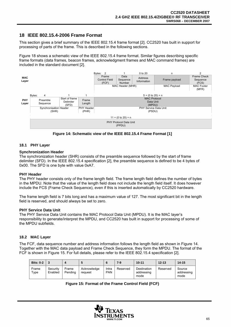
CC2520 DATASHEET2.4 GHZ IEEE 802.15.4/ZIGBEE® RF TRANSCEIVER
SWRS068 – DECEMBER 2007
WWW.TI.COM 65
18 IEEE 802.15.4-2006 Frame Format This section gives a brief summary of the IEEE 802.15.4 frame format [2]. CC2520 has built in support for processing of parts of the frame. This is described in the following sections. Figure 18 shows a schematic view of the IEEE 802.15.4 frame format. Similar figures describing specific frame formats (data frames, beacon frames, acknowledgment frames and MAC command frames) are included in the standard document [2].
PHYLayer
FrameControl Field
(FCF)
DataSequenceNumber
2 1Bytes:
AddressInformation
0 to 20
Frame payload
nFrame Check
Sequence(FCS)
2
MAC Header (MHR) MAC Payload MAC Footer(MFR)
FrameLength
MAC ProtocolData Unit(MPDU)
Start of frameDelimiter
(SFD)
Bytes: 1 1 5 + (0 to 20) + n
PreambleSequence
4
Synchronisation Header(SHR)
PHY Header(PHR)
PHY Service Data Unit(PSDU)
PHY Protocol Data Unit(PPDU)
11 + (0 to 20) + n
MACLayer
Figure 14: Schematic view of the IEEE 802.15.4 Frame Format [1]
18.1 PHY Layer
Synchronization Header The synchronization header (SHR) consists of the preamble sequence followed by the start of frame delimiter (SFD). In the IEEE 802.15.4 specification [2], the preamble sequence is defined to be 4 bytes of 0x00. The SFD is one byte with value 0xA7. PHY Header The PHY header consists only of the frame length field. The frame length field defines the number of bytes in the MPDU. Note that the value of the length field does not include the length field itself. It does however include the FCS (Frame Check Sequence), even if this is inserted automatically by TCC2520 Thardware. The frame length field is 7 bits long and has a maximum value of 127. The most significant bit in the length field is reserved, and should always be set to zero. PHY Service Data Unit The PHY Service Data Unit contains the MAC Protocol Data Unit (MPDU). It is the MAC layer’s responsibility to generate/interpret the MPDU, and CC2520 has built in support for processing of some of the MPDU subfields.
18.2 MAC Layer
The FCF, data sequence number and address information follows the length field as shown in Figure 14. Together with the MAC data payload and Frame Check Sequence, they form the MPDU. The format of the FCF is shown in Figure 15. For full details, please refer to the IEEE 802.15.4 specification [2].
Bits: 0-2 3 4 5 6 7-9 10-11 12-13 14-15
Frame Type
Security Enabled
Frame Pending
Acknowledge request
Intra PAN
Reserved Destination addressing mode
Reserved Source addressing mode
Figure 15: Format of the Frame Control Field (FCF)

CC2520 DATASHEET 2.4 GHZ IEEE 802.15.4/ZIGBEE® RF TRANSCEIVER SWRS068 – DECEMBER 2007
66 WWW.TI.COM
Frame Check Sequence A 2-byte frame check sequence (FCS) follows the last MAC payload byte as shown in Figure 14. The FCS is calculated over the MPDU, i.e. the length field is not part of the FCS. The FCS polynomial defined in [2] is
1)( 51216 +++= xxxxG CCC2520 supports automatic calculation/verification of the FCS. See sections 20.3 and 22.1.3 for details.
CC2520 DATASHEET2.4 GHZ IEEE 802.15.4/ZIGBEE® RF TRANSCEIVER
SWRS068 – DECEMBER 2007
WWW.TI.COM 67
19 Transmit Mode This section describes how to control the transmitter, the integrated frame processing and how to use the TX FIFO.
19.1 TX Control
CC2520 has many built in features for frame processing and status reporting. Note that CC2520 provides features that make it easy for the microcontroller to have precise control of the timing of outgoing frames. This is very important in an IEEE 802.15.4/ZigBee system, because there are strict timing requirements to such systems. Frame transmission will be started by the following actions:
• The STXON command strobe o The SAMPLED_CCA signal is not updated.
• The STXONCCA command strobe, provided that the CCA signal is high. o Aborts ongoing transmission/reception and forces a TX calibration followed by transmission. o The SAMPLED_CCA signal is updated
Clear channel assessment is described in detail in section 19.7. Frame transmission will be aborted by the following command actions:
• The SRXON command strobe o Aborts ongoing transmission and forces a RX calibration
• The SRFOFF command strobe o Aborts ongoing transmission/reception and forces the FSM to the IDLE state.
• The STXON command strobe o See above.
To enable the receiver after transmission with STXON, the FRMCTRL1.SET_RXENMASK_ON_TX bit should be set. This will set bit 14 in RXENABLE when STXON is executed. When transmitting with STXONCCA, the receiver would be on before the transmission and will be turned back on afterwards (unless the RXENABLE registers have been cleared in the mean time).
19.2 TX State Timing
Transmission of preamble begins 192 us after the STXON or STXONCCA command strobe. This is referred to as "TX turnaround time" in [2]. There is an equal delay when returning to receive mode. When returning to idle or receive mode, there is a 2 us delay while the modulator ramps down the signals to the DACs. The down ramping happens automatically after the complete MPDU (as defined by the length byte) has been transmitted or if TX underflow occurs. This affects:
• The SFD signal, which is stretched by 2 us. • The radio FSM transition to the IDLE state, which is delayed by 2 us.
19.3 TX FIFO Access
The TX FIFO can hold 128 bytes and only one frame at a time. The frame can be buffered before or after the TX command strobe is executed, as long as it does not generate TX underflow (see the error conditions listed below). Figure 16 illustrates what needs to be written to the TX FIFO (marked blue). Additional bytes are ignored, unless TX overflow occurs (see the error conditions listed below).
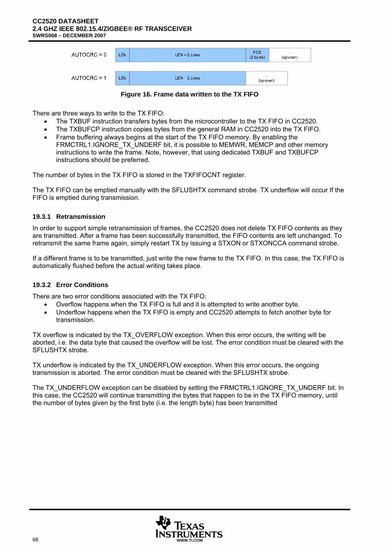
CC2520 DATASHEET 2.4 GHZ IEEE 802.15.4/ZIGBEE® RF TRANSCEIVER SWRS068 – DECEMBER 2007
68 WWW.TI.COM
Figure 16. Frame data written to the TX FIFO
There are three ways to write to the TX FIFO:
• The TXBUF instruction transfers bytes from the microcontroller to the TX FIFO in CC2520. • The TXBUFCP instruction copies bytes from the general RAM in CC2520 into the TX FIFO. • Frame buffering always begins at the start of the TX FIFO memory. By enabling the
FRMCTRL1.IGNORE_TX_UNDERF bit, it is possible to MEMWR, MEMCP and other memory instructions to write the frame. Note, however, that using dedicated TXBUF and TXBUFCP instructions should be preferred.
The number of bytes in the TX FIFO is stored in the TXFIFOCNT register. The TX FIFO can be emptied manually with the SFLUSHTX command strobe. TX underflow will occur If the FIFO is emptied during transmission.
19.3.1 Retransmission
In order to support simple retransmission of frames, the CC2520 does not delete TX FIFO contents as they are transmitted. After a frame has been successfully transmitted, the FIFO contents are left unchanged. To retransmit the same frame again, simply restart TX by issuing a STXON or STXONCCA command strobe. If a different frame is to be transmitted, just write the new frame to the TX FIFO. In this case, the TX FIFO is automatically flushed before the actual writing takes place.
19.3.2 Error Conditions
There are two error conditions associated with the TX FIFO: • Overflow happens when the TX FIFO is full and it is attempted to write another byte. • Underflow happens when the TX FIFO is empty and CC2520 attempts to fetch another byte for
transmission. TX overflow is indicated by the TX_OVERFLOW exception. When this error occurs, the writing will be aborted, i.e. the data byte that caused the overflow will be lost. The error condition must be cleared with the SFLUSHTX strobe. TX underflow is indicated by the TX_UNDERFLOW exception. When this error occurs, the ongoing transmission is aborted. The error condition must be cleared with the SFLUSHTX strobe. The TX_UNDERFLOW exception can be disabled by setting the FRMCTRL1.IGNORE_TX_UNDERF bit. In this case, the CC2520 will continue transmitting the bytes that happen to be in the TX FIFO memory, until the number of bytes given by the first byte (i.e. the length byte) has been transmitted
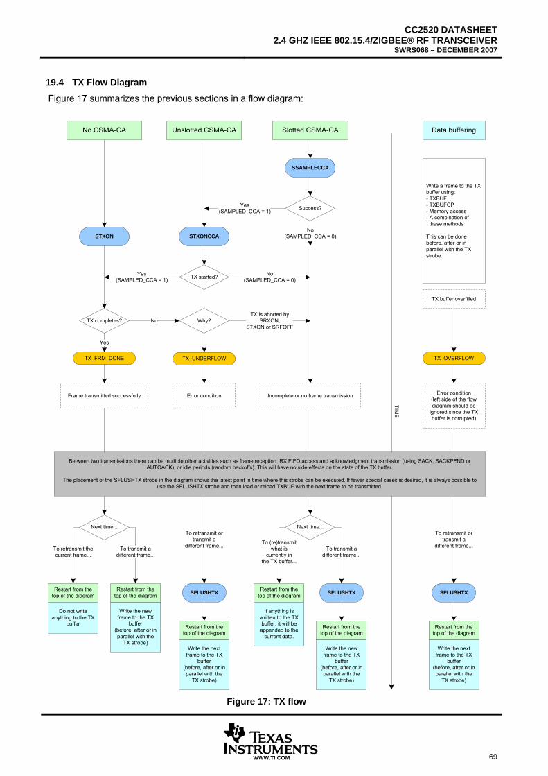
CC2520 DATASHEET2.4 GHZ IEEE 802.15.4/ZIGBEE® RF TRANSCEIVER
SWRS068 – DECEMBER 2007
WWW.TI.COM 69
19.4 TX Flow Diagram
Figure 17 summarizes the previous sections in a flow diagram:
Frame transmitted successfully Incomplete or no frame transmission
Write a frame to the TX buffer using:- TXBUF - TXBUFCP - Memory access- A combination of these methods
This can be done before, after or in parallel with the TX strobe.
STXONCCASTXON
SSAMPLECCA
No
No(SAMPLED_CCA = 0)
Yes(SAMPLED_CCA = 1)
TX completes?
TX_FRM_DONE
TX started?
Yes
Next time...
To retransmit the current frame...
Why?
To retransmit or transmit a
different frame...
TX is aborted by SRXON,
STXON or SRFOFF
TX_OVERFLOW
TX buffer overfilled
Error condition
To transmit a different frame...
Next time...
To (re)transmit what is
currently in the TX buffer...
To transmit a different frame...
SFLUSHTXSFLUSHTX
Error condition(left side of the flow diagram should be
ignored since the TX buffer is corrupted)
TX_UNDERFLOW
To retransmit or transmit a
different frame...
SFLUSHTX
TIME
Write the next frame to the TX
buffer (before, after or in parallel with the
TX strobe)
Write the new frame to the TX
buffer (before, after or in parallel with the
TX strobe)
Write the next frame to the TX
buffer (before, after or in parallel with the
TX strobe)
Write the new frame to the TX
buffer (before, after or in parallel with the
TX strobe)
No(SAMPLED_CCA = 0)
Success?Yes(SAMPLED_CCA = 1)
No CSMA-CA Unslotted CSMA-CA Slotted CSMA-CA
Between two transmissions there can be multiple other activities such as frame reception, RX FIFO access and acknowledgment transmission (using SACK, SACKPEND or AUTOACK), or idle periods (random backoffs). This will have no side effects on the state of the TX buffer.
The placement of the SFLUSHTX strobe in the diagram shows the latest point in time where this strobe can be executed. If fewer special cases is desired, it is always possible to use the SFLUSHTX strobe and then load or reload TXBUF with the next frame to be transmitted.
Restart from the top of the diagram
If anything is written to the TX buffer, it will be
appended to the current data.
Data buffering
Restart from the top of the diagram
Do not write anything to the TX
buffer
Restart from the top of the diagram
Restart from the top of the diagram
Restart from the top of the diagram
Restart from the top of the diagram
Figure 17: TX flow
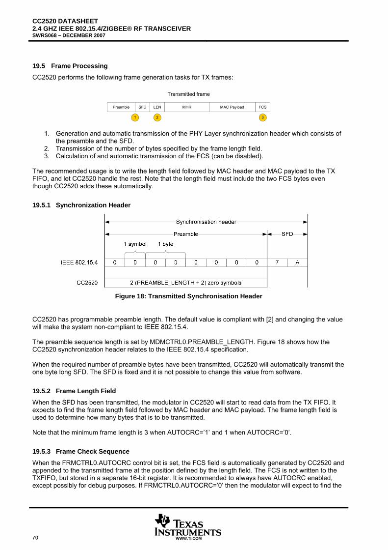
CC2520 DATASHEET 2.4 GHZ IEEE 802.15.4/ZIGBEE® RF TRANSCEIVER SWRS068 – DECEMBER 2007
70 WWW.TI.COM
19.5 Frame Processing
CC2520 performs the following frame generation tasks for TX frames:
Preamble SFD MHR FCSLEN
1 3
MAC Payload
Transmitted frame
2
1. Generation and automatic transmission of the PHY Layer synchronization header which consists of the preamble and the SFD.
2. Transmission of the number of bytes specified by the frame length field. 3. Calculation of and automatic transmission of the FCS (can be disabled).
The recommended usage is to write the length field followed by MAC header and MAC payload to the TX FIFO, and let CC2520 handle the rest. Note that the length field must include the two FCS bytes even though CC2520 adds these automatically.
19.5.1 Synchronization Header
Figure 18: Transmitted Synchronisation Header
TCC2520 has programmable Tpreamble length. The default value is compliant with [2] and changing the value will make the system non-compliant to IEEE 802.15.4. The preamble sequence length is set by MDMCTRL0.PREAMBLE_LENGTH. Figure 18 shows how the TCC2520T synchronization header relates to the IEEE 802.15.4 specification. When the required number of preamble bytes have been transmitted, CC2520 will automatically transmit the one byte long SFD. The SFD is fixed and it is not possible to change this value from software.
19.5.2 Frame Length Field
When the SFD has been transmitted, the modulator in CC2520 will start to read data from the TX FIFO. It expects to find the frame length field followed by MAC header and MAC payload. The frame length field is used to determine how many bytes that is to be transmitted. Note that the minimum frame length is 3 when AUTOCRC=’1’ and 1 when AUTOCRC=’0’.
19.5.3 Frame Check Sequence
When the FRMCTRL0.AUTOCRC control bit is set, the FCS field is automatically generated by CC2520 and appended to the transmitted frame at the position defined by the length field. The FCS is not written to the TXFIFO, but stored in a separate 16-bit register. It is recommended to always have AUTOCRC enabled, except possibly for debug purposes. If FRMCTRL0.AUTOCRC=’0’ then the modulator will expect to find the
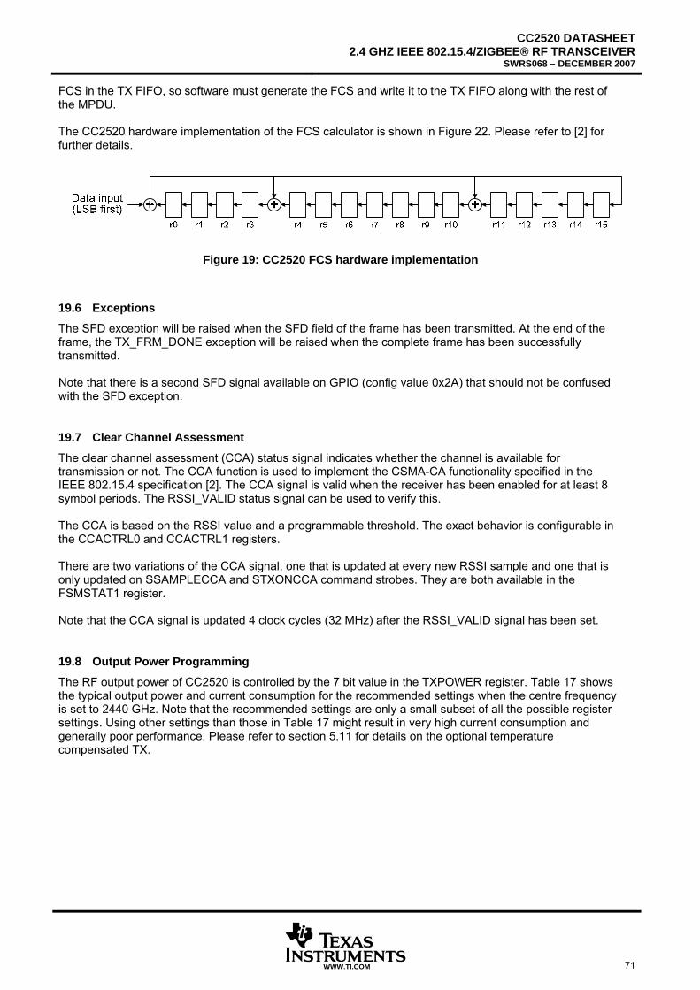
CC2520 DATASHEET2.4 GHZ IEEE 802.15.4/ZIGBEE® RF TRANSCEIVER
SWRS068 – DECEMBER 2007
WWW.TI.COM 71
FCS in the TX FIFO, so software must generate the FCS and write it to the TX FIFO along with the rest of the MPDU. The TCC2520T hardware implementation of the FCS calculator is shown in Figure 22. Please refer to [2] for further details.
Figure 19: CC2520 FCS hardware implementation
19.6 Exceptions
The SFD exception will be raised when the SFD field of the frame has been transmitted. At the end of the frame, the TX_FRM_DONE exception will be raised when the complete frame has been successfully transmitted. Note that there is a second SFD signal available on GPIO (config value 0x2A) that should not be confused with the SFD exception.
19.7 Clear Channel Assessment
The clear channel assessment (CCA) status signal indicates whether the channel is available for transmission or not. The CCA function is used to implement the CSMA-CA functionality specified in the IEEE 802.15.4 specification [2]. The CCA signal is valid when the receiver has been enabled for at least 8 symbol periods. The RSSI_VALID status signal can be used to verify this. The CCA is based on the RSSI value and a programmable threshold. The exact behavior is configurable in the CCACTRL0 and CCACTRL1 registers. There are two variations of the CCA signal, one that is updated at every new RSSI sample and one that is only updated on SSAMPLECCA and STXONCCA command strobes. They are both available in the FSMSTAT1 register. Note that the CCA signal is updated 4 clock cycles (32 MHz) after the RSSI_VALID signal has been set.
19.8 Output Power Programming
The RF output power of CC2520 is controlled by the 7 bit value in the TXPOWER register. Table 17 shows the typical output power and current consumption for the recommended settings when the centre frequency is set to 2440 GHz. Note that the recommended settings are only a small subset of all the possible register settings. Using other settings than those in Table 17 might result in very high current consumption and generally poor performance. Please refer to section 5.11 for details on the optional temperature compensated TX.
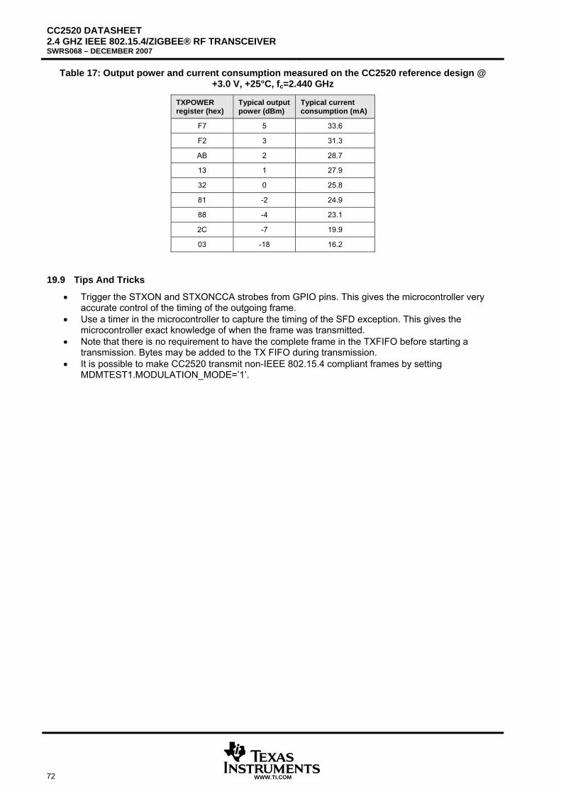
CC2520 DATASHEET 2.4 GHZ IEEE 802.15.4/ZIGBEE® RF TRANSCEIVER SWRS068 – DECEMBER 2007
72 WWW.TI.COM
Table 17: Output power and current consumption measured on the CC2520 reference design @ +3.0 V, +25°C, fc=2.440 GHz
TXPOWER register (hex)
Typical output power (dBm)
Typical current consumption (mA)
F7 5 33.6
F2 3 31.3
AB 2 28.7
13 1 27.9
32 0 25.8
81 -2 24.9
88 -4 23.1
2C -7 19.9
03 -18 16.2
19.9 Tips And Tricks
• Trigger the STXON and STXONCCA strobes from GPIO pins. This gives the microcontroller very accurate control of the timing of the outgoing frame.
• Use a timer in the microcontroller to capture the timing of the SFD exception. This gives the microcontroller exact knowledge of when the frame was transmitted.
• Note that there is no requirement to have the complete frame in the TXFIFO before starting a transmission. Bytes may be added to the TX FIFO during transmission.
• It is possible to make CC2520 transmit non-IEEE 802.15.4 compliant frames by setting MDMTEST1.MODULATION_MODE=’1’.
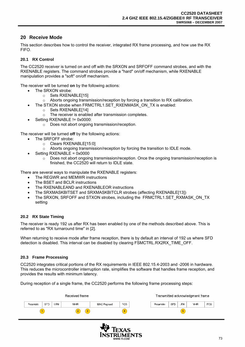
CC2520 DATASHEET2.4 GHZ IEEE 802.15.4/ZIGBEE® RF TRANSCEIVER
SWRS068 – DECEMBER 2007
WWW.TI.COM 73
20 Receive Mode This section describes how to control the receiver, integrated RX frame processing, and how use the RX FIFO.
20.1 RX Control
The CC2520 receiver is turned on and off with the SRXON and SRFOFF command strobes, and with the RXENABLE registers. The command strobes provide a "hard" on/off mechanism, while RXENABLE manipulation provides a "soft" on/off mechanism. The receiver will be turned on by the following actions:
• The SRXON strobe: o Sets RXENABLE[15] o Aborts ongoing transmission/reception by forcing a transition to RX calibration.
• The STXON strobe when FRMCTRL1.SET_RXENMASK_ON_TX is enabled: o Sets RXENABLE[14] o The receiver is enabled after transmission completes.
• Setting RXENABLE != 0x0000: o Does not abort ongoing transmission/reception.
The receiver will be turned off by the following actions:
• The SRFOFF strobe: o Clears RXENABLE[15:0] o Aborts ongoing transmission/reception by forcing the transition to IDLE mode.
• Setting RXENABLE = 0x0000 o Does not abort ongoing transmission/reception. Once the ongoing transmission/reception is
finished, the CC2520 will return to IDLE state. There are several ways to manipulate the RXENABLE registers:
• The REGWR and MEMWR instructions • The BSET and BCLR instructions • The RXENABLEAND and RXENABLEOR instructions • The SRXMASKBITSET and SRXMASKBITCLR strobes (affecting RXENABLE[13]) • The SRXON, SRFOFF and STXON strobes, including the FRMCTRL1.SET_RXMASK_ON_TX
setting
20.2 RX State Timing
The receiver is ready 192 us after RX has been enabled by one of the methods described above. This is referred to as "RX turnaround time" in [2]. When returning to receive mode after frame reception, there is by default an interval of 192 us where SFD detection is disabled. This interval can be disabled by clearing FSMCTRL.RX2RX_TIME_OFF.
20.3 Frame Processing
CC2520 integrates critical portions of the RX requirements in IEEE 802.15.4-2003 and -2006 in hardware. This reduces the microcontroller interruption rate, simplifies the software that handles frame reception, and provides the results with minimum latency. During reception of a single frame, the CC2520 performs the following frame processing steps:
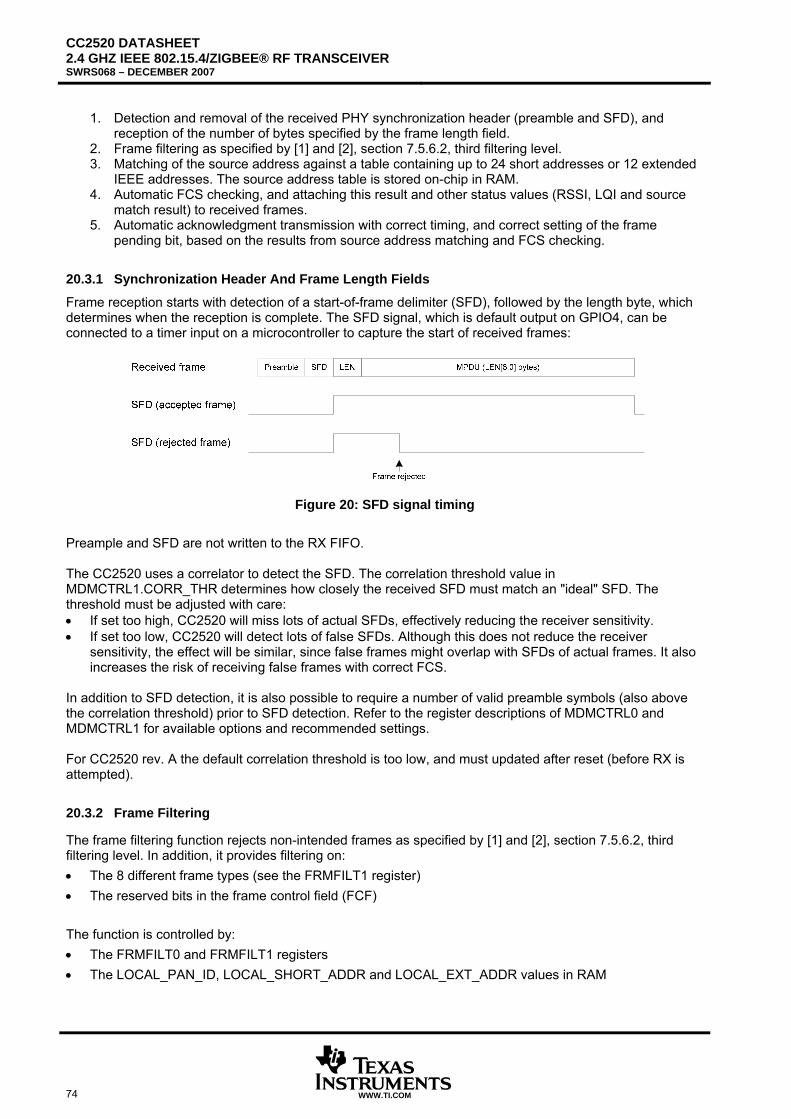
CC2520 DATASHEET 2.4 GHZ IEEE 802.15.4/ZIGBEE® RF TRANSCEIVER SWRS068 – DECEMBER 2007
74 WWW.TI.COM
1. Detection and removal of the received PHY synchronization header (preamble and SFD), and
reception of the number of bytes specified by the frame length field. 2. Frame filtering as specified by [1] and [2], section 7.5.6.2, third filtering level. 3. Matching of the source address against a table containing up to 24 short addresses or 12 extended
IEEE addresses. The source address table is stored on-chip in RAM. 4. Automatic FCS checking, and attaching this result and other status values (RSSI, LQI and source
match result) to received frames. 5. Automatic acknowledgment transmission with correct timing, and correct setting of the frame
pending bit, based on the results from source address matching and FCS checking.
20.3.1 Synchronization Header And Frame Length Fields
Frame reception starts with detection of a start-of-frame delimiter (SFD), followed by the length byte, which determines when the reception is complete. The SFD signal, which is default output on GPIO4, can be connected to a timer input on a microcontroller to capture the start of received frames:
Figure 20: SFD signal timing
Preample and SFD are not written to the RX FIFO. The CC2520 uses a correlator to detect the SFD. The correlation threshold value in MDMCTRL1.CORR_THR determines how closely the received SFD must match an "ideal" SFD. The threshold must be adjusted with care: • If set too high, CC2520 will miss lots of actual SFDs, effectively reducing the receiver sensitivity. • If set too low, CC2520 will detect lots of false SFDs. Although this does not reduce the receiver
sensitivity, the effect will be similar, since false frames might overlap with SFDs of actual frames. It also increases the risk of receiving false frames with correct FCS.
In addition to SFD detection, it is also possible to require a number of valid preamble symbols (also above the correlation threshold) prior to SFD detection. Refer to the register descriptions of MDMCTRL0 and MDMCTRL1 for available options and recommended settings. For CC2520 rev. A the default correlation threshold is too low, and must updated after reset (before RX is attempted).
20.3.2 Frame Filtering
The frame filtering function rejects non-intended frames as specified by [1] and [2], section 7.5.6.2, third filtering level. In addition, it provides filtering on: • The 8 different frame types (see the FRMFILT1 register) • The reserved bits in the frame control field (FCF) The function is controlled by: • The FRMFILT0 and FRMFILT1 registers • The LOCAL_PAN_ID, LOCAL_SHORT_ADDR and LOCAL_EXT_ADDR values in RAM
CC2520 DATASHEET2.4 GHZ IEEE 802.15.4/ZIGBEE® RF TRANSCEIVER
SWRS068 – DECEMBER 2007
WWW.TI.COM 75
Filtering Algorithm The FRMFILT0.FRM_FILTER_EN bit controls whether frame filtering is applied or not. When disabled, the CC2520 will accept all received frames. When enabled (which is the default setting), the CC2520 will only accept frames that fulfill all of the following requirements: • The length byte must be equal to or higher than the “minimum frame length”, which is derived from the
source- and destination address mode and PAN ID compression subfields of the FCF. • The reserved FCF bits [9:7] and’ed together with FRMFILT0.FCF_RESERVED_BITMASK must equal
0b000. • The value of the frame version subfield of the FCF cannot be higher than
FRMFILT0.MAX_FRAME_VERSION. • The source and destination address modes cannot be reserved values (1). • Destination address:
• If a destination PAN ID is included in the frame, it must match LOCAL_PANID or must be the broadcast PAN identifier (0xFFFF).
• If a short destination address is included in the frame, it must match either LOCAL_SHORT_ADDR or the broadcast address (0xFFFF).
• If an extended destination address is included in the frame, it must match LOCAL_EXT_ADDR. • Frame type:
• Beacon frames (0) are only accepted when: • FRMFILT1.ACCEPT_FT0_BEACON = 1 • Length byte >= 9 • The destination address mode is 0 (no destination address) • The source address mode is 2 or 3 (i.e. a source address is included) • The source PAN ID matches LOCAL_PANID, or LOCAL_PANID equals 0xFFFF
• Data (1) frames are only accepted when: • FRMFILT1.ACCEPT_FT1_DATA = 1 • Length byte >= 9 • A destination address and/or source address is included in the frame. If no destination address
is included in the frame, the FRMFILT0.PAN_COORDINATOR bit must be set and the source PAN ID must equal LOCAL_PANID.
• Acknowledgment (2) frames are only accepted when: • FRMFILT1.ACCEPT_FT2_ACK = 1 • Length byte = 5
• MAC command (3) frames are only accepted when: • FRMFILT1.ACCEPT_FT3_MAC_CMD = 1 • Length byte >= 9 • A destination address and/or source address is included in the frame. If no destination address
is included in the frame, the FRMFILT0.PAN_COORDINATOR bit must be set and the source PAN ID must equal LOCAL_PANID for the frame to be accepted..
• Reserved frame types (4, 5, 6 and 7) are only accepted when: • FRMFILT1.ACCEPT_FT4TO7_RESERVED = 1 (default is 0) • Length byte >= 9
The following operations are performed before the filtering begins, with no effect on the frame data stored in the RX FIFO:
• Bit 7 of the length byte is masked out (don’t care). • If FRMFILT1.MODIFY_FT_FILTER is unlike zero, the MSB of the frame type subfield of the FCF is
either inverted or forced to 0 or 1.
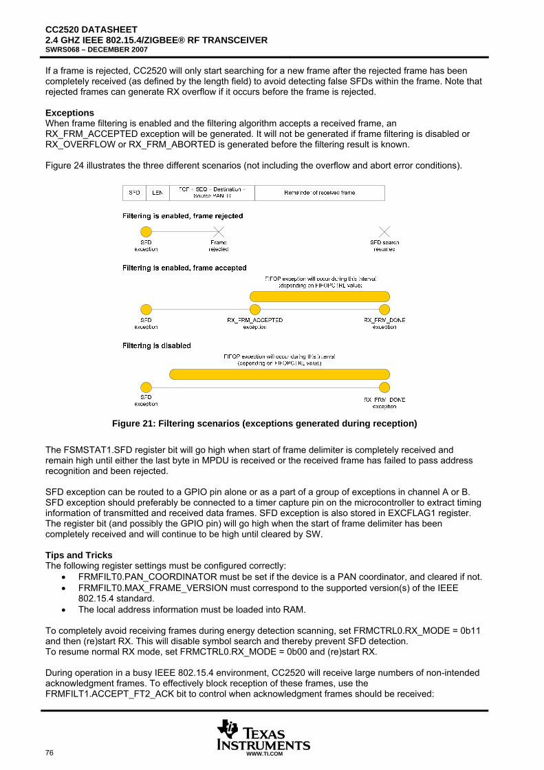
CC2520 DATASHEET 2.4 GHZ IEEE 802.15.4/ZIGBEE® RF TRANSCEIVER SWRS068 – DECEMBER 2007
76 WWW.TI.COM
If a frame is rejected, CC2520 will only start searching for a new frame after the rejected frame has been completely received (as defined by the length field) to avoid detecting false SFDs within the frame. Note that rejected frames can generate RX overflow if it occurs before the frame is rejected. Exceptions When frame filtering is enabled and the filtering algorithm accepts a received frame, an RX_FRM_ACCEPTED exception will be generated. It will not be generated if frame filtering is disabled or RX_OVERFLOW or RX_FRM_ABORTED is generated before the filtering result is known. Figure 24 illustrates the three different scenarios (not including the overflow and abort error conditions).
Figure 21: Filtering scenarios (exceptions generated during reception)
The FSMSTAT1.SFD register bit will go high when start of frame delimiter is completely received and remain high until either the last byte in MPDU is received or the received frame has failed to pass address recognition and been rejected. SFD exception can be routed to a GPIO pin alone or as a part of a group of exceptions in channel A or B. SFD exception should preferably be connected to a timer capture pin on the microcontroller to extract timing information of transmitted and received data frames. SFD exception is also stored in EXCFLAG1 register. The register bit (and possibly the GPIO pin) will go high when the start of frame delimiter has been completely received and will continue to be high until cleared by SW. Tips and Tricks The following register settings must be configured correctly:
• FRMFILT0.PAN_COORDINATOR must be set if the device is a PAN coordinator, and cleared if not. • FRMFILT0.MAX_FRAME_VERSION must correspond to the supported version(s) of the IEEE
802.15.4 standard. • The local address information must be loaded into RAM.
To completely avoid receiving frames during energy detection scanning, set FRMCTRL0.RX_MODE = 0b11 and then (re)start RX. This will disable symbol search and thereby prevent SFD detection. To resume normal RX mode, set FRMCTRL0.RX_MODE = 0b00 and (re)start RX. During operation in a busy IEEE 802.15.4 environment, CC2520 will receive large numbers of non-intended acknowledgment frames. To effectively block reception of these frames, use the FRMFILT1.ACCEPT_FT2_ACK bit to control when acknowledgment frames should be received:
CC2520 DATASHEET2.4 GHZ IEEE 802.15.4/ZIGBEE® RF TRANSCEIVER
SWRS068 – DECEMBER 2007
WWW.TI.COM 77
• Set FRMFILT1.ACCEPT_FT2_ACK after successfully starting a transmission with acknowledgment request, and clear the bit again after the acknowledgment frame has been received, or the timeout has been reached.
• Keep the bit cleared otherwise. It is not necessary to turn off the receiver while changing the values of the FRMFILT0/1 registers and the local address information stored in RAM. However, if the changes take place between reception of the SFD byte and the source PAN ID (i.e. between the SFD and RX_FRM_ACCEPTED exceptions), the modified values must be considered as don’t care for that particular frame (CC2520 will use either the old or the new value). Note that it is possible to make CC2520 ignore all IEEE 802.15.4 incoming frames by setting MDMTEST1.MODULATION_MODE=’1’.
20.3.3 Source Address Matching
CC2520 supports matching of the source address in received frames against a table stored in the on-chip memory. The table is 96 bytes long, and hence it can contain up to:
• 24 short addresses (2 + 2 bytes each) • 12 IEEE extended addresses (8 bytes each).
Source address matching will only be performed when frame filtering is also enabled, and the received frame has been accepted. The function is controlled by:
• The SRCMATCH, SRCSHORTEN0, SRCSHORTEN1, SRCSHORTEN2, SRCEXTEN0, SRCEXTEN1 and SRCEXTEN2 registers
• The source address table in RAM. Applications Automatic acknowledgment transmission with correct setting of the frame pending bit: When using indirect frame transmission, the devices will send data requests to poll frames stored on the coordinator. To indicate whether it actually has a frame stored for the device, the coordinator must set or clear the frame pending bit in the returned acknowledgment frame. On most 8- and 16-bit MCUs, however, there is not enough time to determine this, and so the coordinator ends up setting the pending bit regardless of whether there are pending frames for the device (as required by IEEE 802.15.4 [2]). This is wasteful in terms of power consumption, because the polling device will have to keep its receiver enabled for a considerable period of time, even if there are no frames for it. By loading the destination addresses in the indirect frame queue into the source address table and enabling the AUTOPEND function, CC2520 will set the pending bit in outgoing acknowledgment frames automatically. This way the operation is no longer timing critical, as the effort done by the microcontroller is when adding or removing frames in the indirect frame queue and updating the source address table accordingly. Security material look-up: To reduce the time needed to process secured frames, the source address table can be set up so the entries match the table of security keys on the microcontroller. A second level of masking on the table entries allows this application to be combined with automatic setting of the pending bit in acknowledgment frames. Other applications: The two previous applications are the main targets for the source address matching function. However, for proprietary protocols that only rely on the basic IEEE 802.15.4 frame format, there are several other useful applications. For instance, by using it together with the exception binding mechanism, it is possible to create firewall functionality where only a specified set of nodes will be acknowledged. The Source Address Table The source address table begins at address 0x380 in RAM as shown in Figure 11. The space is shared between short and extended addresses, and the SRCSHORTEN0/1/2 and SRCEXTEN0/1/2 registers are used to control which entries are enabled. All values in the table are little-endian (as in the received frames).
• A short address entry starts with the 16-bit PAN ID followed by the 16-bit short address. These entries are stored at address 0x380 + (4 × n), where n is a number between 0 and 23.
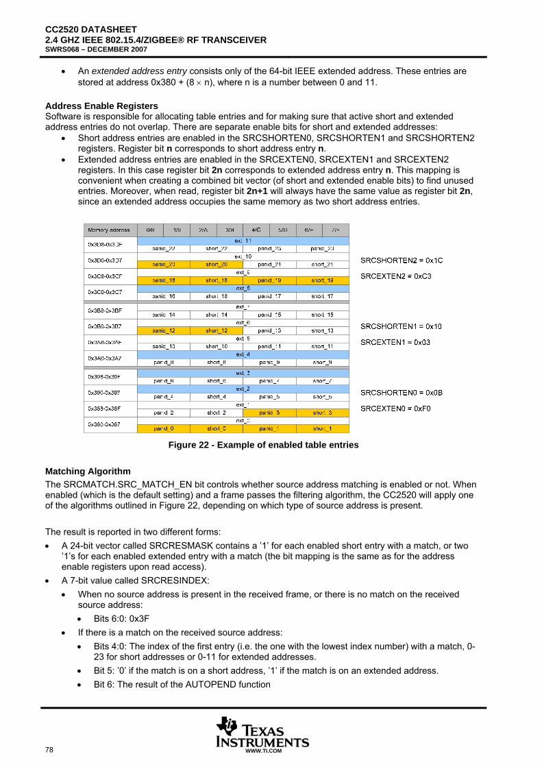
CC2520 DATASHEET 2.4 GHZ IEEE 802.15.4/ZIGBEE® RF TRANSCEIVER SWRS068 – DECEMBER 2007
78 WWW.TI.COM
• An extended address entry consists only of the 64-bit IEEE extended address. These entries are stored at address 0x380 + (8 × n), where n is a number between 0 and 11.
Address Enable Registers Software is responsible for allocating table entries and for making sure that active short and extended address entries do not overlap. There are separate enable bits for short and extended addresses:
• Short address entries are enabled in the SRCSHORTEN0, SRCSHORTEN1 and SRCSHORTEN2 registers. Register bit n corresponds to short address entry n.
• Extended address entries are enabled in the SRCEXTEN0, SRCEXTEN1 and SRCEXTEN2 registers. In this case register bit 2n corresponds to extended address entry n. This mapping is convenient when creating a combined bit vector (of short and extended enable bits) to find unused entries. Moreover, when read, register bit 2n+1 will always have the same value as register bit 2n, since an extended address occupies the same memory as two short address entries.
Figure 22 - Example of enabled table entries
Matching Algorithm The SRCMATCH.SRC_MATCH_EN bit controls whether source address matching is enabled or not. When enabled (which is the default setting) and a frame passes the filtering algorithm, the CC2520 will apply one of the algorithms outlined in Figure 22, depending on which type of source address is present. The result is reported in two different forms: • A 24-bit vector called SRCRESMASK contains a ’1’ for each enabled short entry with a match, or two
’1’s for each enabled extended entry with a match (the bit mapping is the same as for the address enable registers upon read access).
• A 7-bit value called SRCRESINDEX: • When no source address is present in the received frame, or there is no match on the received
source address: • Bits 6:0: 0x3F
• If there is a match on the received source address: • Bits 4:0: The index of the first entry (i.e. the one with the lowest index number) with a match, 0-
23 for short addresses or 0-11 for extended addresses. • Bit 5: ’0’ if the match is on a short address, ’1’ if the match is on an extended address. • Bit 6: The result of the AUTOPEND function
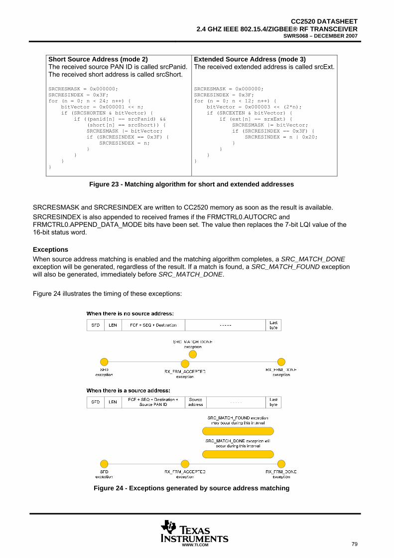
CC2520 DATASHEET2.4 GHZ IEEE 802.15.4/ZIGBEE® RF TRANSCEIVER
SWRS068 – DECEMBER 2007
WWW.TI.COM 79
Short Source Address (mode 2) The received source PAN ID is called srcPanid. The received short address is called srcShort. SRCRESMASK = 0x000000; SRCRESINDEX = 0x3F; for (n = 0; n < 24; n++) bitVector = 0x000001 << n; if (SRCSHORTEN & bitVector) if ((panid[n] == srcPanid) && (short[n] == srcShort)) SRCRESMASK |= bitVector; if (SRCRESINDEX == 0x3F) SRCRESINDEX = n;
Extended Source Address (mode 3) The received extended address is called srcExt. SRCRESMASK = 0x000000; SRCRESINDEX = 0x3F; for (n = 0; n < 12; n++) bitVector = 0x000003 << (2*n); if (SRCEXTEN & bitVector) if (ext[n] == srxExt) SRCRESMASK |= bitVector; if (SRCRESINDEX == 0x3F) SRCRESINDEX = n | 0x20;
Figure 23 - Matching algorithm for short and extended addresses
SRCRESMASK and SRCRESINDEX are written to CC2520 memory as soon as the result is available. SRCRESINDEX is also appended to received frames if the FRMCTRL0.AUTOCRC and FRMCTRL0.APPEND_DATA_MODE bits have been set. The value then replaces the 7-bit LQI value of the 16-bit status word. Exceptions When source address matching is enabled and the matching algorithm completes, a SRC_MATCH_DONE exception will be generated, regardless of the result. If a match is found, a SRC_MATCH_FOUND exception will also be generated, immediately before SRC_MATCH_DONE. Figure 24 illustrates the timing of these exceptions:
Figure 24 - Exceptions generated by source address matching
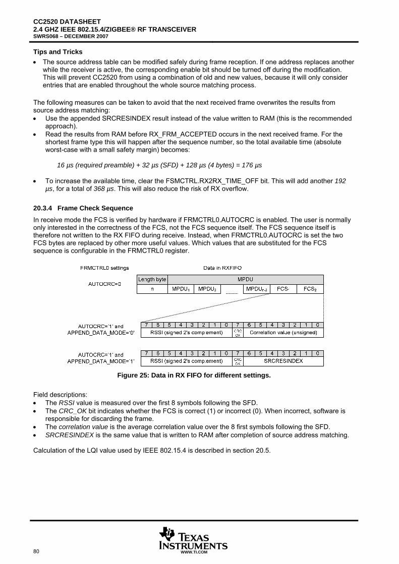
CC2520 DATASHEET 2.4 GHZ IEEE 802.15.4/ZIGBEE® RF TRANSCEIVER SWRS068 – DECEMBER 2007
80 WWW.TI.COM
Tips and Tricks • The source address table can be modified safely during frame reception. If one address replaces another
while the receiver is active, the corresponding enable bit should be turned off during the modification. This will prevent CC2520 from using a combination of old and new values, because it will only consider entries that are enabled throughout the whole source matching process.
The following measures can be taken to avoid that the next received frame overwrites the results from source address matching: • Use the appended SRCRESINDEX result instead of the value written to RAM (this is the recommended
approach). • Read the results from RAM before RX_FRM_ACCEPTED occurs in the next received frame. For the
shortest frame type this will happen after the sequence number, so the total available time (absolute worst-case with a small safety margin) becomes:
16 µs (required preamble) + 32 µs (SFD) + 128 µs (4 bytes) = 176 µs
• To increase the available time, clear the FSMCTRL.RX2RX_TIME_OFF bit. This will add another 192 µs, for a total of 368 µs. This will also reduce the risk of RX overflow.
20.3.4 Frame Check Sequence
In receive mode the FCS is verified by hardware if FRMCTRL0.AUTOCRC is enabled. The user is normally only interested in the correctness of the FCS, not the FCS sequence itself. The FCS sequence itself is therefore not written to the RX FIFO during receive. Instead, when FRMCTRL0.AUTOCRC is set the two FCS bytes are replaced by other more useful values. Which values that are substituted for the FCS sequence is configurable in the FRMCTRL0 register.
Figure 25: Data in RX FIFO for different settings.
Field descriptions: • The RSSI value is measured over the first 8 symbols following the SFD. • The CRC_OK bit indicates whether the FCS is correct (1) or incorrect (0). When incorrect, software is
responsible for discarding the frame. • The correlation value is the average correlation value over the 8 first symbols following the SFD. • SRCRESINDEX is the same value that is written to RAM after completion of source address matching. Calculation of the LQI value used by IEEE 802.15.4 is described in section 20.5.
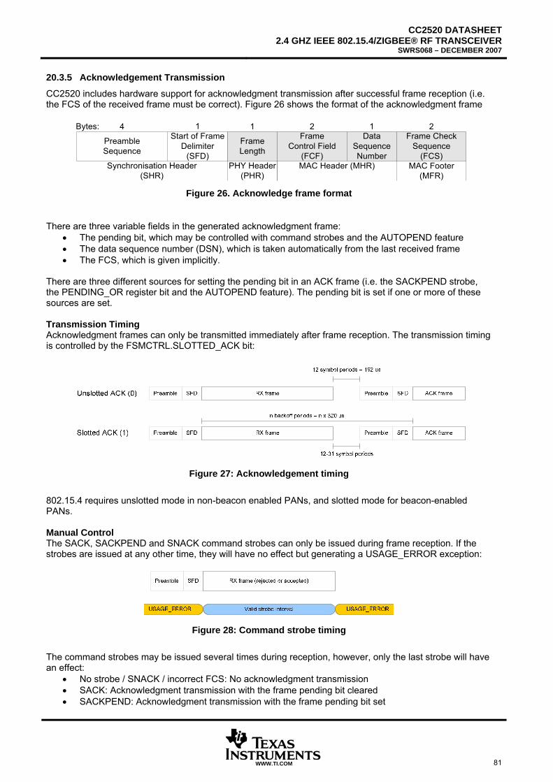
CC2520 DATASHEET2.4 GHZ IEEE 802.15.4/ZIGBEE® RF TRANSCEIVER
SWRS068 – DECEMBER 2007
WWW.TI.COM 81
20.3.5 Acknowledgement Transmission
TCC2520T includes hardware support for acknowledgment transmission after successful frame reception (i.e. the FCS of the received frame must be correct). Figure 26 shows the format of the acknowledgment frame
FrameControl Field
(FCF)
DataSequenceNumber
2 1Frame Check
Sequence(FCS)
2
MAC Header (MHR) MAC Footer(MFR)
FrameLength
Start of FrameDelimiter
(SFD)
Bytes: 1 1
PreambleSequence
4
Synchronisation Header(SHR)
PHY Header(PHR)
Figure 26. Acknowledge frame format
There are three variable fields in the generated acknowledgment frame:
• The pending bit, which may be controlled with command strobes and the AUTOPEND feature • The data sequence number (DSN), which is taken automatically from the last received frame • The FCS, which is given implicitly.
There are three different sources for setting the pending bit in an ACK frame (i.e. the SACKPEND strobe, the PENDING_OR register bit and the AUTOPEND feature). The pending bit is set if one or more of these sources are set. Transmission Timing Acknowledgment frames can only be transmitted immediately after frame reception. The transmission timing is controlled by the FSMCTRL.SLOTTED_ACK bit:
Figure 27: Acknowledgement timing
802.15.4 requires unslotted mode in non-beacon enabled PANs, and slotted mode for beacon-enabled PANs. Manual Control The SACK, SACKPEND and SNACK command strobes can only be issued during frame reception. If the strobes are issued at any other time, they will have no effect but generating a USAGE_ERROR exception:
Figure 28: Command strobe timing
The command strobes may be issued several times during reception, however, only the last strobe will have an effect:
• No strobe / SNACK / incorrect FCS: No acknowledgment transmission • SACK: Acknowledgment transmission with the frame pending bit cleared • SACKPEND: Acknowledgment transmission with the frame pending bit set
CC2520 DATASHEET 2.4 GHZ IEEE 802.15.4/ZIGBEE® RF TRANSCEIVER SWRS068 – DECEMBER 2007
82 WWW.TI.COM
Automatic Control (AUTOACK) When FRMFILT0.FRM_FILTER_EN and FRMCTRL0.AUTOACK are both enabled, the CC2520 will determine automatically whether or not to transmit acknowledgment frames:
• The RX frame must be accepted by frame filtering (indicated by the RX_FRM_ACCEPTED exception)
• The acknowledgment request bit must be set in the RX frame • The RX frame must not be a beacon or an acknowledgment frame • The FCS of the RX frame must be correct
Automatic acknowledgments can be overridden by the SACK, SACKPEND and SNACK command strobes. For instance, if the microcontroller is low on memory resources and cannot store a received frame, the SNACK strobe can be issued during reception and prevent acknowledging the discarded frame. By default, the AUTOACK feature never sets the frame pending bit in the acknowledgment frames. Apart from manual override with command strobes, there are two options:
• Automatic control, using the AUTOPEND feature • Manual control, using the FRMCTRL1.PENDING_OR bit
Automatic Setting of the Frame Pending Field (AUTOPEND) When the SRCMATCH.AUTOPEND bit is set, the result from source address matching determines the value of the frame pending field. Upon reception of a frame, the frame pending field in the (possibly) returned acknowledgment will be set, given that:
• FRMFILT0.FRAME_FILTER_EN is set. • SRCMATCH.SRC_MATCH_EN is set. • SRCMATCH.AUTOPEND is set. • The received frame matches the current SRCMATCH.PEND_DATAREQ_ONLY setting. • The received source address matches at least one source match table entry, which is enabled in
both SRCSHORTEN and SRCSHORTPENDEN, or SRCEXTEN and SRCEXTPENDEN. If the source matching table runs full, the FRMCTRL1.PENDING_OR bit may be used to override the AUTOPEND feature and temporarily acknowledge all frames with the frame pending field set.
20.4 RX FIFO Access
The RX FIFO can hold one or more received frames, provided that the total number of bytes is 128 or less. There are two ways to determine the number of bytes in the RX FIFO:
• Reading RXFIFOCNT register • Using the FIFOP and FIFO signals in combination with the FIFOPCTRL.FIFOPTHR setting
There are several ways to access the RX FIFO:
• The RXBUF instruction transfers received bytes from CC2520 to the microcontroller • The RXBUFCP instruction transfers received bytes from CC2520 to the microcontroller and makes
a copy of the read bytes in CC2520 RAM • The RXBUFMOV instruction transfers received bytes from the RX FIFO to CC2520 RAM • The RXFIRST register allows software to peek at the head byte in the RX FIFO
The SFLUSHRX command strobe resets the RX FIFO, removing all received frames, and clearing all counters, status signals and sticky error conditions.
20.4.1 Using the FIFO and FIFOP Signals
The FIFO and FIFOP signals are useful when reading out received frames in small portions while the frame is received:
• The FIFO signal (default output on GPIO1) goes high when there is one or more bytes in the RX FIFO, but low when RX overflow has occurred.
• The FIFOP signal (default output on GPIO2) goes high when
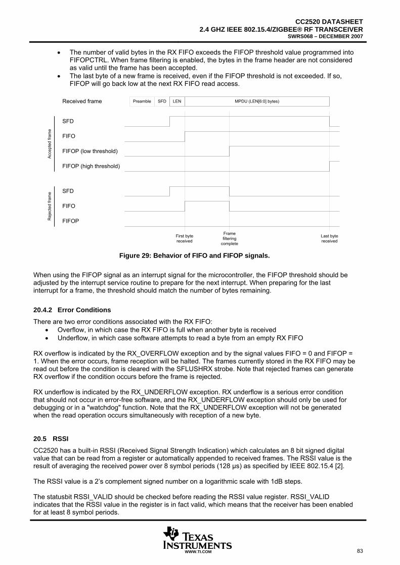
CC2520 DATASHEET2.4 GHZ IEEE 802.15.4/ZIGBEE® RF TRANSCEIVER
SWRS068 – DECEMBER 2007
WWW.TI.COM 83
• The number of valid bytes in the RX FIFO exceeds the FIFOP threshold value programmed into FIFOPCTRL. When frame filtering is enabled, the bytes in the frame header are not considered as valid until the frame has been accepted.
• The last byte of a new frame is received, even if the FIFOP threshold is not exceeded. If so, FIFOP will go back low at the next RX FIFO read access.
SFD
Received frame Preamble SFD LEN MPDU (LEN[6:0] bytes)
FIFO
FIFOP (low threshold)
FIFOP (high threshold)
Acce
pted
fram
eR
ejec
ted
fram
e SFD
FIFO
FIFOP
First byte received
Frame filtering
complete
Last byte received
Figure 29: Behavior of FIFO and FIFOP signals.
When using the FIFOP signal as an interrupt signal for the microcontroller, the FIFOP threshold should be adjusted by the interrupt service routine to prepare for the next interrupt. When preparing for the last interrupt for a frame, the threshold should match the number of bytes remaining.
20.4.2 Error Conditions
There are two error conditions associated with the RX FIFO: • Overflow, in which case the RX FIFO is full when another byte is received • Underflow, in which case software attempts to read a byte from an empty RX FIFO
RX overflow is indicated by the RX_OVERFLOW exception and by the signal values FIFO = 0 and FIFOP = 1. When the error occurs, frame reception will be halted. The frames currently stored in the RX FIFO may be read out before the condition is cleared with the SFLUSHRX strobe. Note that rejected frames can generate RX overflow if the condition occurs before the frame is rejected. RX underflow is indicated by the RX_UNDERFLOW exception. RX underflow is a serious error condition that should not occur in error-free software, and the RX_UNDERFLOW exception should only be used for debugging or in a "watchdog" function. Note that the RX_UNDERFLOW exception will not be generated when the read operation occurs simultaneously with reception of a new byte.
20.5 RSSI
CC2520 has a built-in RSSI (Received Signal Strength Indication) which calculates an 8 bit signed digital value that can be read from a register or automatically appended to received frames. The RSSI value is the result of averaging the received power over 8 symbol periods (128 µs) as specified by IEEE 802.15.4 [2]. The RSSI value is a 2’s complement signed number on a logarithmic scale with 1dB steps. The statusbit RSSI_VALID should be checked before reading the RSSI value register. RSSI_VALID indicates that the RSSI value in the register is in fact valid, which means that the receiver has been enabled for at least 8 symbol periods.
CC2520 DATASHEET 2.4 GHZ IEEE 802.15.4/ZIGBEE® RF TRANSCEIVER SWRS068 – DECEMBER 2007
84 WWW.TI.COM
To find the actual signal power P at the RF pins with reasonable accuracy, an offset has to be added to the RSSI value.
P = RSSI - OFFSET [dBm] The offset is an empirical value which is found during characterization and is approximately 76 dBm for the CC2520 reference design. E.g. reading a RSSI value of -10 from the RSSI register means that the RF input power is approximately -86 dBm. It is configurable how CC2520 updates the RSSI register after it has first become valid. If FRMCTRL0.ENERGY_SCAN=’0’ (default), the RSSI register contains the latest value available, but if this bit is set to ‘1’, a peak search is performed and the RSSI register will contain the largest value since the energy scan was enabled.
20.6 Link Quality Indication
The link quality indication (LQI) is a measurement of the strength and/or quality of the received frame as defined by the IEEE 802.15.4 standard [2]. The LQI value is required by the IEEE 802.15.4 standard [2] to be limited to the range 0 through 255, with at least 8 unique values. CC2520 does not provide a LQI value directly, but reports several measurements that can be used by the microcontroller to calculate a LQI value. The RSSI value may be used by the MAC software to calculate the LQI value. This approach has the disadvantage that e.g. a narrowband interferer inside the channel bandwidth will increase the RSSI and thus the LQI value although it actually reduces the true link quality. CC2520 therefore also provides an average correlation value for each incoming frame, based on the 8 first symbols following the SFD. This unsigned 7-bit value can be looked upon as a measurement of the “chip error rate,” although CC2520 does not do chip decision. As described in section 20.3.4, the average correlation value for the 8 first symbols is appended to each received frame together with the RSSI and CRC OK/not OK when MDMCTRL0.AUTOCRC is set. A correlation value of ~110 indicates a maximum quality frame while a value of ~50 is typically the lowest quality frames detectable by CC2520. Software must convert the correlation value to the range 0-255 as defined by [2], for instance by calculating:
LQI = (CORR - a)b limited to the range 0-255, where a and b are found empirically based on PER measurements as a function of the correlation value. A combination of RSSI and correlation values may also be used to generate the LQI value.
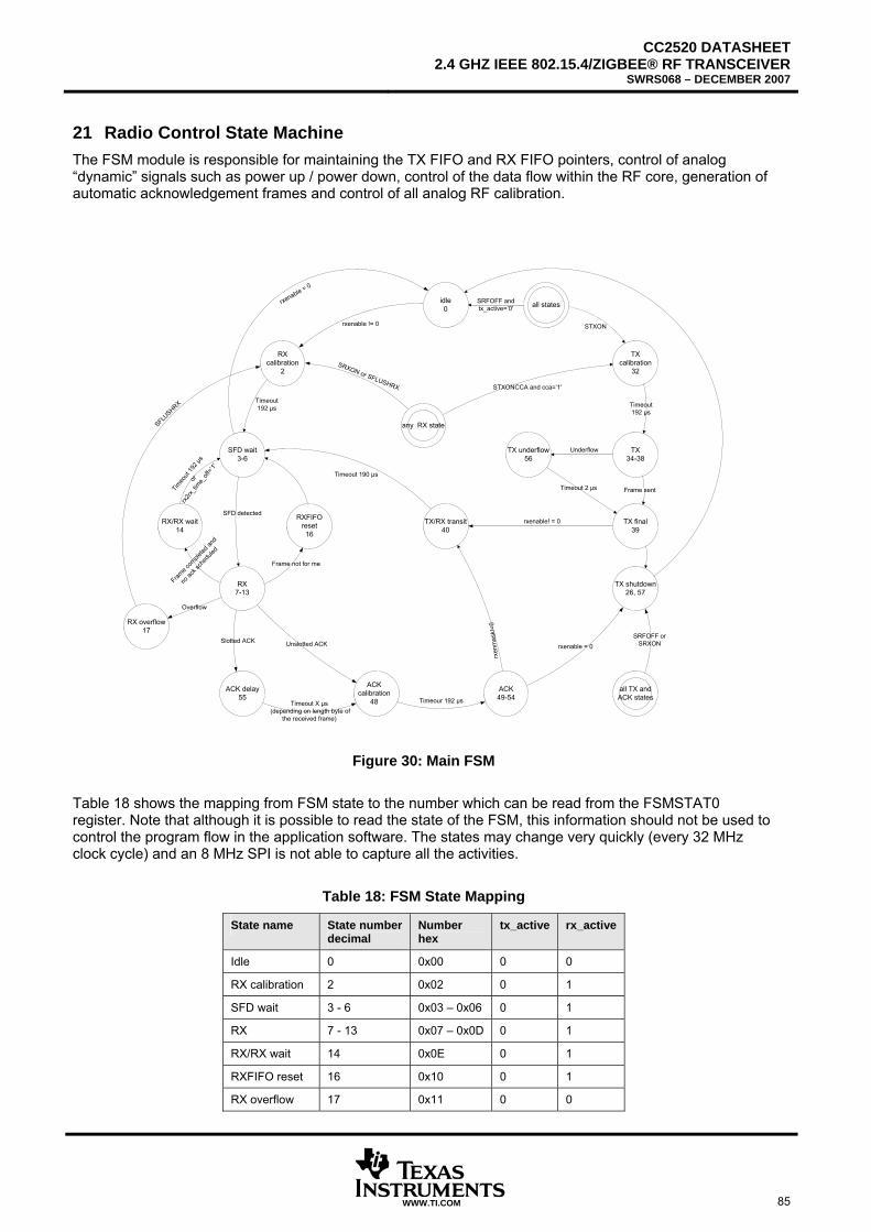
CC2520 DATASHEET2.4 GHZ IEEE 802.15.4/ZIGBEE® RF TRANSCEIVER
SWRS068 – DECEMBER 2007
WWW.TI.COM 85
21 Radio Control State Machine The FSM module is responsible for maintaining the TX FIFO and RX FIFO pointers, control of analog “dynamic” signals such as power up / power down, control of the data flow within the RF core, generation of automatic acknowledgement frames and control of all analog RF calibration.
RX calibration
2
SFD wait3-6
TX calibration
32
TX34-38
ACK calibration
48
STXON
Timeout192 µs
Timeout192 µs
RXFIFO reset16
rxenable! = 0
all states
Frame c
omple
ted an
d
no ac
k sch
edule
d
ACK49-54
rxen
mas
k!=0
RX overflow17
any RX state
STXONCCA and cca=’1'
TX final39
Frame sent
idle0
TX/RX transit40
Timeout 190 µs
RX7-13
SRXON or SFLUSHRX
RX/RX wait14
Timeo
ut 19
2 µs
or
rx2rx_
time_
off=’1
'
ACK delay55
TX underflow56
all TX and ACK states
TX shutdown26, 57
SFD detected
SRFOFF andtx_active=’0'
rxenable != 0
rxenable = 0
Timeour 192 µsTimeout X µs (depending on length byte of
the received frame)
Unslotted ACKSlotted ACK
Overflow
Frame not for me
SFLUSHRX
SRFOFF orSRXONrxenable = 0
Timeout 2 µs
Underflow
Figure 30: Main FSM
Table 18 shows the mapping from FSM state to the number which can be read from the FSMSTAT0 register. Note that although it is possible to read the state of the FSM, this information should not be used to control the program flow in the application software. The states may change very quickly (every 32 MHz clock cycle) and an 8 MHz SPI is not able to capture all the activities.
Table 18: FSM State Mapping
State name State numberdecimal
Number hex
tx_active rx_active
Idle 0 0x00 0 0
RX calibration 2 0x02 0 1
SFD wait 3 - 6 0x03 – 0x06 0 1
RX 7 - 13 0x07 – 0x0D 0 1
RX/RX wait 14 0x0E 0 1
RXFIFO reset 16 0x10 0 1
RX overflow 17 0x11 0 0

CC2520 DATASHEET 2.4 GHZ IEEE 802.15.4/ZIGBEE® RF TRANSCEIVER SWRS068 – DECEMBER 2007
86 WWW.TI.COM
State name State numberdecimal
Number hex
tx_active rx_active
TX calibration 32 0x20 1 0
TX 34 - 38 0x22 – 0x26 1 0
TX final 39 0x27 1 0
TX/RX transit 40 0x28 1 0
ACK calibration 48 0x30 1 0
ACK 49 - 54 0x31 – 0x36 1 0
ACK delay 55 0x37 1 0
TX underflow 56 0x38 1 0
TX shutdown 26, 57 0x1A, 0x39 1 0
CC2520 DATASHEET2.4 GHZ IEEE 802.15.4/ZIGBEE® RF TRANSCEIVER
SWRS068 – DECEMBER 2007
WWW.TI.COM 87
22 Crystal Oscillator The internal crystal oscillator generates the main frequency reference. The reference frequency must be 32 MHz. Because the crystal frequency is used as reference for the data rate as well as other internal signal processing functions, other frequencies cannot be used. The crystal must be connected between the XOSC32M_Q1 and XOSC32M_Q2 pins. The oscillator is designed for parallel mode operation of the crystal. In addition, loading capacitors (C121 and C131) for the crystal are required. The loading capacitor values depend on the total load capacitance, CL, specified for the crystal. The total load capacitance seen between the crystal terminals should equal CL for the crystal to oscillate at the specified frequency. CC2520 has the ability to add more capacitance in order to tune the oscillator frequency. The amount of extra capacitance is configurable with the FREQTUNE register.
131121
111
CC
CCC parasitictuneL
+++=
The parasitic capacitance is constituted by pin input capacitance and PCB stray capacitance. The total parasitic capacitance is typically 2 pF - 5 pF. Note that the default value for the FREQTUNE register means “no added capacitance”, which means that only reduction of the frequency is possible. By reducing the external capacitors (C121 and C131), the default frequency is increased. This way, the actual frequency tuning range can be moved so that both positive and negative tuning around the target frequency is possible. The crystal oscillator is amplitude regulated. This means that a high current is used to start up the oscillations. When the amplitude builds up, the current is reduced to what is necessary to maintain a stable oscillation. This ensures a fast start-up and keeps the drive level to a minimum. The ESR of the crystal must be within the specification in order to ensure a reliable start-up. See section 6 for crystal specific parameters (including tuning).
CC2520 DATASHEET 2.4 GHZ IEEE 802.15.4/ZIGBEE® RF TRANSCEIVER SWRS068 – DECEMBER 2007
88 WWW.TI.COM
23 External Clock Output CC2520 can provide a 50-50 duty cycle clock signal to external circuits. This is an advantage for low-cost systems where one wants as few components as possible, because both the microcontroller and CC2520 can run on the same crystal. CC2520 has a clock divider that can make glitch free changes between many different frequencies between 1 and 16 MHz. After a reset, CC2520 will output a 1MHz clock on GPIO0. Note that CC2520 needs to be in active mode in order for the crystal oscillator to be running and thus have the ability to provide an external clock. The procedure for waking a system up from LPM2 is as follows:
• MCU is running on RC oscillator, CC2520 is in LPM2 • Change CC2520 from LPM2 to active mode. • Switch the MCU over to the 1 MHz clock that CC2520 outputs on GPIO0. • Change to the desired clock frequency.
The procedure for bringing a system from active mode to LPM2 is as follows:
• Switch MCU over to RC oscillator. • Set CC2520 in LPM2.
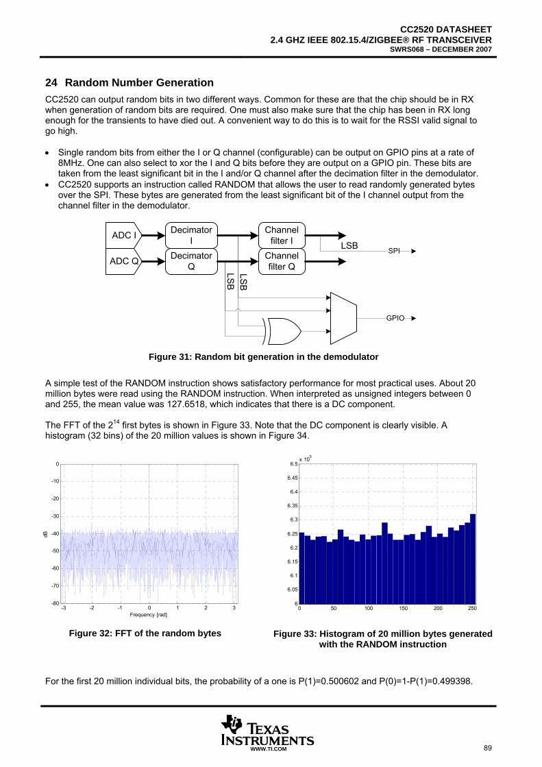
CC2520 DATASHEET2.4 GHZ IEEE 802.15.4/ZIGBEE® RF TRANSCEIVER
SWRS068 – DECEMBER 2007
WWW.TI.COM 89
24 Random Number Generation CC2520 can output random bits in two different ways. Common for these are that the chip should be in RX when generation of random bits are required. One must also make sure that the chip has been in RX long enough for the transients to have died out. A convenient way to do this is to wait for the RSSI valid signal to go high. • Single random bits from either the I or Q channel (configurable) can be output on GPIO pins at a rate of
8MHz. One can also select to xor the I and Q bits before they are output on a GPIO pin. These bits are taken from the least significant bit in the I and/or Q channel after the decimation filter in the demodulator.
• CC2520 supports an instruction called RANDOM that allows the user to read randomly generated bytes over the SPI. These bytes are generated from the least significant bit of the I channel output from the channel filter in the demodulator.
ADC I
ADC Q
Decimator I
Decimator Q
Channel filter I
Channel filter Q
GPIO
LSB
LSB
SPILSB
Figure 31: Random bit generation in the demodulator
A simple test of the RANDOM instruction shows satisfactory performance for most practical uses. About 20 million bytes were read using the RANDOM instruction. When interpreted as unsigned integers between 0 and 255, the mean value was 127.6518, which indicates that there is a DC component. The FFT of the 214 first bytes is shown in Figure 33. Note that the DC component is clearly visible. A histogram (32 bins) of the 20 million values is shown in Figure 34.
-3 -2 -1 0 1 2 3-80
-70
-60
-50
-40
-30
-20
-10
0
dB
Frequency [rad] Figure 32: FFT of the random bytes
0 50 100 150 200 2506
6.05
6.1
6.15
6.2
6.25
6.3
6.35
6.4
6.45
6.5x 10⁵
Figure 33: Histogram of 20 million bytes generated with the RANDOM instruction
For the first 20 million individual bits, the probability of a one is P(1)=0.500602 and P(0)=1-P(1)=0.499398.

CC2520 DATASHEET 2.4 GHZ IEEE 802.15.4/ZIGBEE® RF TRANSCEIVER SWRS068 – DECEMBER 2007
90 WWW.TI.COM
Note that to fully qualify the random generator as “true random”, much more elaborate tests are required. There are software packages available on the internet that may be useful in this respect [8], [9].
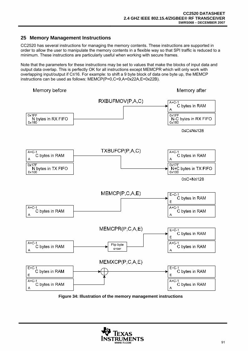
CC2520 DATASHEET2.4 GHZ IEEE 802.15.4/ZIGBEE® RF TRANSCEIVER
SWRS068 – DECEMBER 2007
WWW.TI.COM 91
25 Memory Management Instructions CC2520 has several instructions for managing the memory contents. These instructions are supported in order to allow the user to manipulate the memory contents in a flexible way so that SPI traffic is reduced to a minimum. These instructions are particularly useful when working with secure frames. Note that the parameters for these instructions may be set to values that make the blocks of input data and output data overlap. This is perfectly OK for all instructions except MEMCPR which will only work with overlapping input/output if C≤16. For example: to shift a 9 byte block of data one byte up, the MEMCP instructions can be used as follows: MEMCP(P=0,C=9,A=0x22A,E=0x22B).
Figure 34: Illustration of the memory management instructions
CC2520 DATASHEET 2.4 GHZ IEEE 802.15.4/ZIGBEE® RF TRANSCEIVER SWRS068 – DECEMBER 2007
92 WWW.TI.COM
25.1 RXBUFMOV
The RXBUFMOV instruction reads data from the RX FIFO and places the data at a specified memory location as illustrated in Figure 35.
25.2 TXBUFCP
The TXBUFCP instruction copies a block of data starting at a specified memory location into the TX FIFO as illustrated in Figure 35.
25.3 MEMCP
The MEMCP instruction copies a block of data starting at a specified memory location into another memory location as illustrated in Figure 35.
25.4 MEMCPR
The MEMCPR instruction copies a block of data starting at a specified memory location into another memory location while reversing the endianess. In other words the byte at memory location A+n is copied to memory location E+C-1-n.
25.5 MEMXCP
The MEMXCP instruction xors two blocks of data and writes the result back to the memory location of the second block. This is primarily used as a subroutine for some of the security instructions. It can also be used to clear (set to zero) blocks of RAM with one short SPI instruction. By using the same source and target address, the data is xor’ed with itself, which always results in zero being written back to the RAM.
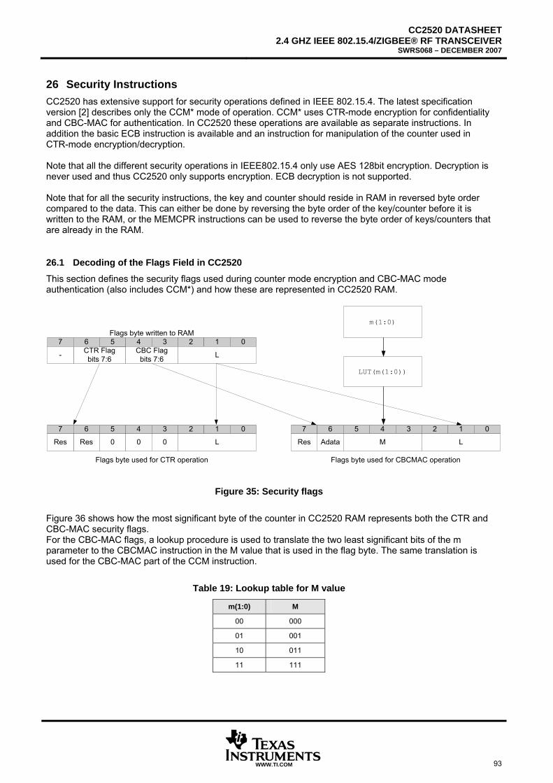
CC2520 DATASHEET2.4 GHZ IEEE 802.15.4/ZIGBEE® RF TRANSCEIVER
SWRS068 – DECEMBER 2007
WWW.TI.COM 93
26 Security Instructions CC2520 has extensive support for security operations defined in IEEE 802.15.4. The latest specification version [2] describes only the CCM* mode of operation. CCM* uses CTR-mode encryption for confidentiality and CBC-MAC for authentication. In CC2520 these operations are available as separate instructions. In addition the basic ECB instruction is available and an instruction for manipulation of the counter used in CTR-mode encryption/decryption. Note that all the different security operations in IEEE802.15.4 only use AES 128bit encryption. Decryption is never used and thus CC2520 only supports encryption. ECB decryption is not supported. Note that for all the security instructions, the key and counter should reside in RAM in reversed byte order compared to the data. This can either be done by reversing the byte order of the key/counter before it is written to the RAM, or the MEMCPR instructions can be used to reverse the byte order of keys/counters that are already in the RAM.
26.1 Decoding of the Flags Field in CC2520
This section defines the security flags used during counter mode encryption and CBC-MAC mode authentication (also includes CCM*) and how these are represented in CC2520 RAM.
7 6CTR Flag bits 7:6
5 4 3 2 1 0
- CBC Flag bits 7:6 L
7 6
Res
5 4 3 2 1 0
L
7 6
Adata
5 4 3 2 1 0
M L0 0 0
m(1:0)
Flags byte written to RAM
Flags byte used for CTR operation
Res Res
LUT(m(1:0))
Flags byte used for CBCMAC operation
Figure 35: Security flags
Figure 36 shows how the most significant byte of the counter in CC2520 RAM represents both the CTR and CBC-MAC security flags. For the CBC-MAC flags, a lookup procedure is used to translate the two least significant bits of the m parameter to the CBCMAC instruction in the M value that is used in the flag byte. The same translation is used for the CBC-MAC part of the CCM instruction.
Table 19: Lookup table for M value
m(1:0) M
00 000
01 001
10 011
11 111
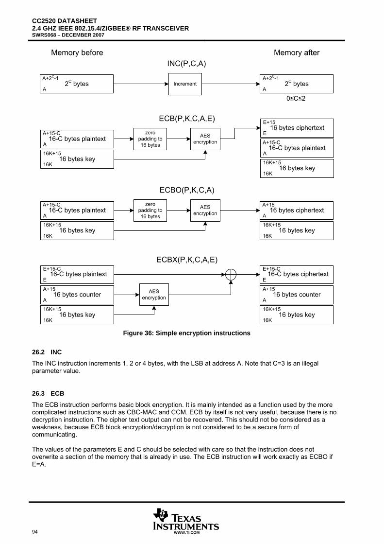
CC2520 DATASHEET 2.4 GHZ IEEE 802.15.4/ZIGBEE® RF TRANSCEIVER SWRS068 – DECEMBER 2007
94 WWW.TI.COM
16 bytes key16K
16K+15
16-C bytes plaintextA
A+15-C
ECB(P,K,C,A,E)16 bytes ciphertext
E
E+15
16 bytes key16K
16K+15
ECBX(P,K,C,A,E)
16-C bytes plaintextE
E+15-C
16 bytes counterA
A+15
AES encryption
zero padding to 16 bytes
AES encryption
16 bytes key16K
16K+15
16-C bytes plaintextA
A+15-C
16 bytes key16K
16K+15
16-C bytes plaintextA
A+15-C
ECBO(P,K,C,A)
AES encryption
zero padding to 16 bytes
16 bytes key16K
16K+15
16 bytes ciphertextA
A+15
16 bytes key16K
16K+15
16-C bytes ciphertextE
E+15-C
16 bytes counterA
A+15
Memory before Memory after
2C bytesA
A+2C-1
INC(P,C,A)
Increment 2C bytesA
A+2C-1
0≤C≤2
Figure 36: Simple encryption instructions
26.2 INC
The INC instruction increments 1, 2 or 4 bytes, with the LSB at address A. Note that C=3 is an illegal parameter value.
26.3 ECB
The ECB instruction performs basic block encryption. It is mainly intended as a function used by the more complicated instructions such as CBC-MAC and CCM. ECB by itself is not very useful, because there is no decryption instruction. The cipher text output can not be recovered. This should not be considered as a weakness, because ECB block encryption/decryption is not considered to be a secure form of communicating. The values of the parameters E and C should be selected with care so that the instruction does not overwrite a section of the memory that is already in use. The ECB instruction will work exactly as ECBO if E=A.

CC2520 DATASHEET2.4 GHZ IEEE 802.15.4/ZIGBEE® RF TRANSCEIVER
SWRS068 – DECEMBER 2007
WWW.TI.COM 95
26.4 ECBO
The ECBO instruction is identical to ECB, except that it will store its output to the same memory locations as the input was read from. It will always output 16 bytes even though the input was not a full 16 bytes.
26.5 ECBX
The ECBX instruction is identical to ECB, except that it will bitwise XOR the result from the encryption with the memory contents of the output address. The values of the parameters E and C should be selected with care so that the instruction does not overwrite a section of the memory that is already in use. The ECBX instruction will work exactly as ECBXO if E=A. Note that the terminology from counter mode encryption is used in Figure 37.
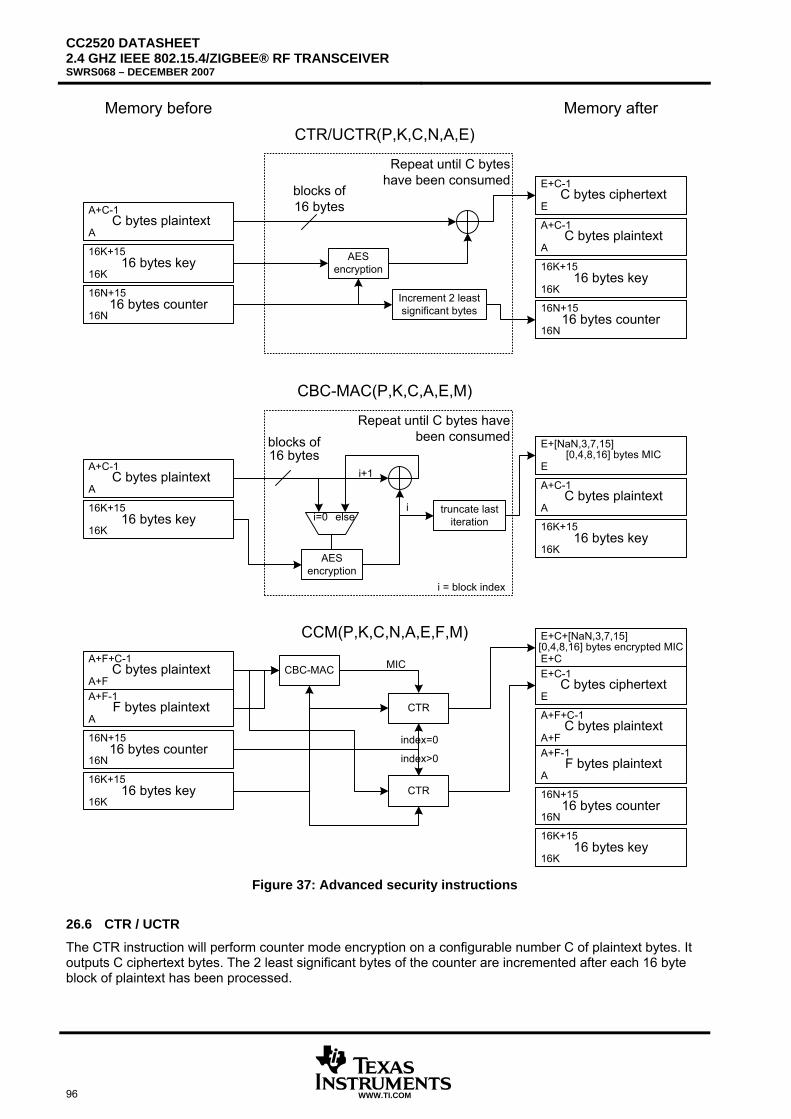
CC2520 DATASHEET 2.4 GHZ IEEE 802.15.4/ZIGBEE® RF TRANSCEIVER SWRS068 – DECEMBER 2007
96 WWW.TI.COM
Repeat until C bytes have been consumed
16 bytes counter16N
16N+15
CTR/UCTR(P,K,C,N,A,E)
C bytes plaintextA
A+C-1
16 bytes key16K
16K+15 AES encryption
16 bytes counter16N
16N+15
C bytes plaintextA
A+C-1
16 bytes key16K
16K+15
C bytes ciphertext
Increment 2 least significant bytes
blocks of 16 bytes E
E+C-1
CBC-MAC(P,K,C,A,E,M)
16 bytes key16K
16K+15
16 bytes key16K
16K+15
16 bytes counter16N
16N+15
CCM(P,K,C,N,A,E,F,M)
F bytes plaintextA
A+F-1
16 bytes key16K
16K+15
16 bytes counter16N
16N+15
16 bytes key16K
16K+15
C bytes ciphertextE
E+C-1C bytes plaintextA+F
A+F+C-1[0,4,8,16] bytes encrypted MICE+C
E+C+[NaN,3,7,15]
F bytes plaintextA
A+F-1
C bytes plaintextA+F
A+F+C-1
CTR
C bytes plaintextA
A+C-1
Repeat until C bytes have been consumed
AES encryption
blocks of 16 bytes
C bytes plaintextA
A+C-1
[0,4,8,16] bytes MICE
E+[NaN,3,7,15]
i=0truncate last
iterationelse
CBC-MAC
CTR
i
i+1
Memory before Memory after
i = block index
MIC
index=0
index>0
Figure 37: Advanced security instructions
26.6 CTR / UCTR
The CTR instruction will perform counter mode encryption on a configurable number C of plaintext bytes. It outputs C ciphertext bytes. The 2 least significant bytes of the counter are incremented after each 16 byte block of plaintext has been processed.
CC2520 DATASHEET2.4 GHZ IEEE 802.15.4/ZIGBEE® RF TRANSCEIVER
SWRS068 – DECEMBER 2007
WWW.TI.COM 97
If the last block of plaintext is not 16 bytes long, only the required number of bits (from the MSB end) from the encryption is used in the XOR operation. The UCTR instruction performs counter mode decryption and is absolutely identical to the CTR instruction because counter mode encryption and decryption are symmetrical operations.
26.7 CBC-MAC
The CBC-MAC instruction performs authentication. Note that if M[1:0]=0 no authentication code is output. For other values of M[1:0] the number of authentication bytes that are output is 2M[1:0]+1. If M[2]=0 the plaintext data is prefixed with the value of C expanded to 8 bits by concatenation of a 0 at the MSB end.
26.8 CCM / UCCM
The CCM instruction uses both CBC-MAC and CTR to perform both authentication and encryption. It supports the CCM* mode of operation as specified in IEEE 802.14.5-2006 [2]. The authentication (CBC-MAC) part calculates a Message Integrity Code (MIC) over the address range A to A+F+C-1. The resulting MIC is encrypted with CTR mode encryption using the counter value with index 0. The encryption (CTR) part encrypts the address range A+F to A+F+C-1 using CTR mode encryption and counter values with index 1 and up, and thus generates C bytes of ciphertext. The output which is the concatenation of the ciphertext and the encrypted MIC is written to memory starting at address E. The UCCM instruction decrypts the ciphertext in the address range A+F to A+F+C-1 using CTR mode decryption. A MIC is then generated in the same way as for the CCM instruction, and compared to the MIC in the input data. The result of the MIC comparison is stored in the DPUSTAT register.
26.8.1 Inputs to the CCM and UCCM Instructions
The input parameters to the CCM and UCCM instructions are described in detail in Figure 38 and Figure 39 with notes on how they related to the terminology used in the IEEE 802.15.4 specifications.
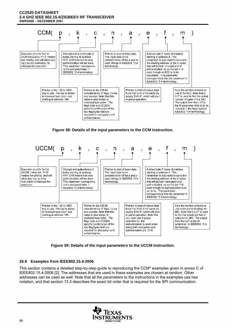
CC2520 DATASHEET 2.4 GHZ IEEE 802.15.4/ZIGBEE® RF TRANSCEIVER SWRS068 – DECEMBER 2007
98 WWW.TI.COM
Figure 38: Details of the input parameters to the CCM instruction.
Figure 39: Details of the input parameters to the UCCM instruction.
26.9 Examples from IEEE802.15.4-2006
This section contains a detailed step-by-step guide to reproducing the CCM* examples given in annex C of IEEE802.15.4-2006 [2]. The addresses that are used in these examples are chosen at random. Other addresses can be used as well. Note that all the parameters to the instructions in the examples use hex notation, and that section 13.3 describes the exact bit order that is required for the SPI communication.
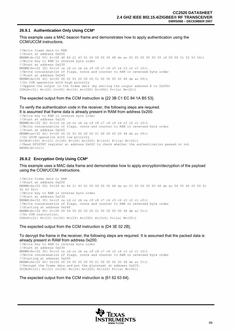
CC2520 DATASHEET2.4 GHZ IEEE 802.15.4/ZIGBEE® RF TRANSCEIVER
SWRS068 – DECEMBER 2007
WWW.TI.COM 99
26.9.1 Authentication Only Using CCM*
This example uses a MAC beacon frame and demonstrates how to apply authentication using the CCM/UCCM instructions. //Write frame data to RAM //Start at address 0x200 MEMWR(A=02 00 D=08 d0 84 21 43 01 00 00 00 00 48 de ac 02 05 00 00 00 55 cf 00 00 51 52 53 54) //Write key to RAM in reverse byte order //Start at address 0x230 MEMWR(A=02 30 D=cf ce cd cc cb ca c9 c8 c7 c6 c5 c4 c3 c2 c1 c0) //Write concatenation of flags, nonce and counter to RAM in reversed byte order //Start at address 0x240 MEMWR(A=02 40 D=00 00 02 05 00 00 00 01 00 00 00 00 48 de ac 09) //Do CCM operation with high priority //Append the output to the frame data (by setting the output address E to 0x000) CCM(P=01 K=23 C=00 N=24 A=200 E=000 F=1a M=02) The expected output from the CCM instruction is 22 3B C1 EC 84 1A B5 53. To verify the authentication code in the receiver, the following steps are required. It is assumed that frame data is already present in RAM from address 0x200. //Write key to RAM in reverse byte order //Start at address 0x230 MEMWR(A=02 30 D=cf ce cd cc cb ca c9 c8 c7 c6 c5 c4 c3 c2 c1 c0) //Write concatenation of flags, nonce and counter to RAM in reversed byte order //Start at address 0x240 MEMWR(a=02 40 D=00 00 02 05 00 00 00 01 00 00 00 00 48 de ac 09) //Do UCCM operation with low priority UCCM(P=00 K=23 C=00 N=24 A=200 E=2c0 F=1a M=02) //Read DPUSTAT register at address 0x02C to check whether the authentication passed or not REGRD(A=2c)
26.9.2 Encryption Only Using CCM*
This example uses a MAC data frame and demonstrates how to apply encryption/decryption of the payload using the CCM/UCCM instructions. //Write frame data to RAM //Start at address 0x200 MEMWR(A=02 00 D=69 dc 84 21 43 02 00 00 00 00 48 de ac 01 00 00 00 00 48 de ac 04 05 00 00 00 61 62 63 64) //Write key to RAM in reverse byte order //Start at address 0x230 MEMWR(A=02 30 D=cf ce cd cc cb ca c9 c8 c7 c6 c5 c4 c3 c2 c1 c0) //Write concatenation of flags, nonce and counter to RAM in reversed byte order //Starting at address 0x240 MEMWR(A=02 40 D=00 00 04 05 00 00 00 01 00 00 00 00 48 de ac 01) //Do CCM instruction. CCM(P=01 K=23 C=04 N=24 A=200 E=2c0 F=1a M=00) The expected output from the CCM instruction is D4 3E 02 2B. To decrypt the frame in the receiver, the following steps are required. It is assumed that the packed data is already present in RAM from address 0x200. //Write key to RAM in reverse byte order //Start at address 0x230 MEMWR(A=02 30 D=cf ce cd cc cb ca c9 c8 c7 c6 c5 c4 c3 c2 c1 c0) //Write concatenation of flags, nonce and counter to RAM in reversed byte order //Starting at address 0x240 MEMWR(A=02 40 D=00 00 04 05 00 00 00 01 00 00 00 00 48 de ac 01) //Decrypt the frame data and put the plaintext at address 0x2C0. UCCM(P=01 K=23 C=04 N=24 A=200 E=2c0 F=1a M=00) The expected output from the CCM instruction is 61 62 63 64.
CC2520 DATASHEET 2.4 GHZ IEEE 802.15.4/ZIGBEE® RF TRANSCEIVER SWRS068 – DECEMBER 2007
100 WWW.TI.COM
26.9.3 Combination of Encryption and Authentication Using CCM*
This example uses a MAC command frame and demonstrates how to apply both encryption/decryption and authentication using the CCM/UCCM instructions. //Write frame data to RAM //Start at address 0x200 MEMWR(A=02 00 D=2b dc 84 21 43 02 00 00 00 00 48 de ac ff ff 01 00 00 00 00 48 de ac 06 05 00 00 00 01 CE) //Write key to RAM in reverse byte order //Start at address 0x230 MEMWR(A=02 30 D=cf ce cd cc cb ca c9 c8 c7 c6 c5 c4 c3 c2 c1 c0) //Write concatenation of flags, nonce and counter to RAM in reversed byte order //Starting at address 0x240 MEMWR(A=02 40 D=00 00 06 05 00 00 00 01 00 00 00 00 48 de ac 09) //Do CCM instruction. //Replace the last byte in the plaintext frame with the cipehertext and encrypted MIC by setting the output address E to 0x000. CCM(P=01 K=23 C=01 N=24 A=200 E=000 F=1d M=02) The expected output from the CCM instruction is D8 4F DE 52 90 61 F9 C6 F1. To decrypt the frame in the receiver, the following steps are required. It is assumed that the packed data is already present in RAM from address 0x200. //Write key to RAM in reverse byte order //Start at address 0x230 MEMWR(A=02 30 D=cf ce cd cc cb ca c9 c8 c7 c6 c5 c4 c3 c2 c1 c0) //Write concatenation of flags, nonce and counter to RAM in reversed byte order //Starting at address 0x240 MEMWR(A=02 40 D=00 00 06 05 00 00 00 01 00 00 00 00 48 de ac 09) //Decrypt the frame data and authenticate the MIC. Note that the output address E is set to 0x000. UCCM(P=01 K=23 C=01 N=24 A=200 E=000 F=1d M=02) //Read DPUSTAT register at address 0x02C to check whether the authentication passed or not REGRD(A=2c) The expected plaintext output from the UCCM instruction is CE.

CC2520 DATASHEET2.4 GHZ IEEE 802.15.4/ZIGBEE® RF TRANSCEIVER
SWRS068 – DECEMBER 2007
WWW.TI.COM 101
27 Packet Sniffing Packet sniffing is a non-intrusive way of observing data that is either being transmitted or received by CC2520. The packet sniffer outputs a clock and a data signal which should be sampled on the rising edges of the clock. The two packet sniffer signals are observable as GPIO outputs. For accurate time stamping, the SFD signal should also be output. Because CC2520 only supports a data rate of 250kbps, the packet sniffer clock frequency is 250 kHz. The data is output serially with the MSB of each byte first, which is opposite of the actual RF transmission, but more convenient when processing the data. It is possible to use an SPI slave to receive the data stream. When sniffing frames in TX mode, the data that is read from the TX FIFO by the modulator is the same data that is output by the packet sniffer. However, if automatic CRC generation is enabled, the packet sniffer will NOT output these 2 bytes. Instead, it will replace the CRC bytes with 0x8080. This value can never occur as the last two bytes of a received frame (when automatic CRC checking is enabled), and thus it provides a way for the receiver of the sniffed data to separate frames that were transmitted by the CC2520 and frames that were received by the CC2520. When sniffing frames in RX mode, the data that is written to the RX FIFO by the demodulator is the same data that is output by the packet sniffer. In other words, the last two bytes are either the received CRC value or the CRC OK/RSSI/correlation/SRCRESINDEX value that may automatically replace the CRC value, depending on configuration settings. Note that in order to observe the packet sniffing data on GPIO pins, the packet sniffer module must be enabled in the MDMTEST1 register, and the correct GPIO configuration must be written to any of the GPIOn registers.
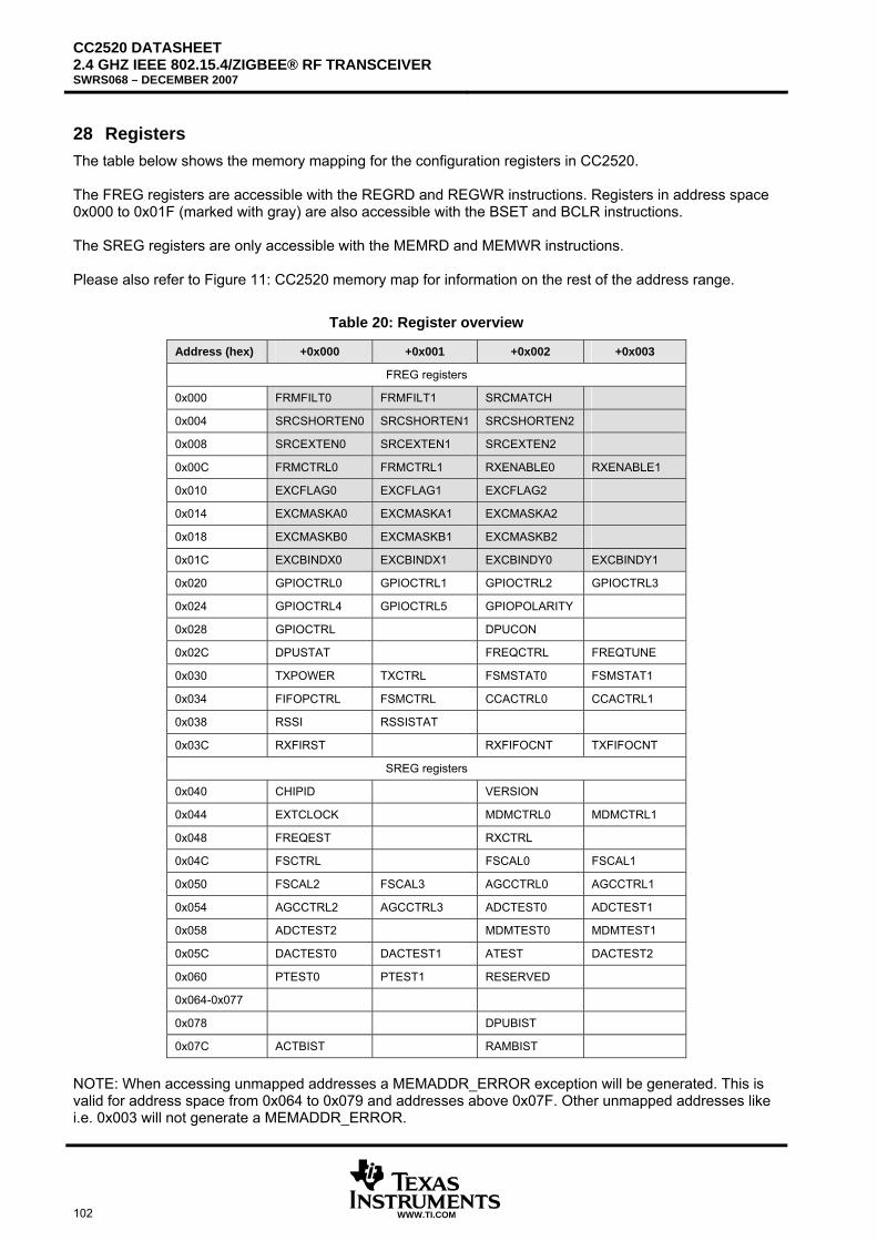
CC2520 DATASHEET 2.4 GHZ IEEE 802.15.4/ZIGBEE® RF TRANSCEIVER SWRS068 – DECEMBER 2007
102 WWW.TI.COM
28 Registers The table below shows the memory mapping for the configuration registers in CC2520. The FREG registers are accessible with the REGRD and REGWR instructions. Registers in address space 0x000 to 0x01F (marked with gray) are also accessible with the BSET and BCLR instructions. The SREG registers are only accessible with the MEMRD and MEMWR instructions. Please also refer to Figure 11: CC2520 memory map for information on the rest of the address range.
Table 20: Register overview
Address (hex) +0x000 +0x001 +0x002 +0x003
FREG registers
0x000 FRMFILT0 FRMFILT1 SRCMATCH
0x004 SRCSHORTEN0 SRCSHORTEN1 SRCSHORTEN2
0x008 SRCEXTEN0 SRCEXTEN1 SRCEXTEN2
0x00C FRMCTRL0 FRMCTRL1 RXENABLE0 RXENABLE1
0x010 EXCFLAG0 EXCFLAG1 EXCFLAG2
0x014 EXCMASKA0 EXCMASKA1 EXCMASKA2
0x018 EXCMASKB0 EXCMASKB1 EXCMASKB2
0x01C EXCBINDX0 EXCBINDX1 EXCBINDY0 EXCBINDY1
0x020 GPIOCTRL0 GPIOCTRL1 GPIOCTRL2 GPIOCTRL3
0x024 GPIOCTRL4 GPIOCTRL5 GPIOPOLARITY
0x028 GPIOCTRL DPUCON
0x02C DPUSTAT FREQCTRL FREQTUNE
0x030 TXPOWER TXCTRL FSMSTAT0 FSMSTAT1
0x034 FIFOPCTRL FSMCTRL CCACTRL0 CCACTRL1
0x038 RSSI RSSISTAT
0x03C RXFIRST RXFIFOCNT TXFIFOCNT
SREG registers
0x040 CHIPID VERSION
0x044 EXTCLOCK MDMCTRL0 MDMCTRL1
0x048 FREQEST RXCTRL
0x04C FSCTRL FSCAL0 FSCAL1
0x050 FSCAL2 FSCAL3 AGCCTRL0 AGCCTRL1
0x054 AGCCTRL2 AGCCTRL3 ADCTEST0 ADCTEST1
0x058 ADCTEST2 MDMTEST0 MDMTEST1
0x05C DACTEST0 DACTEST1 ATEST DACTEST2
0x060 PTEST0 PTEST1 RESERVED
0x064-0x077
0x078 DPUBIST
0x07C ACTBIST RAMBIST
NOTE: When accessing unmapped addresses a MEMADDR_ERROR exception will be generated. This is valid for address space from 0x064 to 0x079 and addresses above 0x07F. Other unmapped addresses like i.e. 0x003 will not generate a MEMADDR_ERROR.
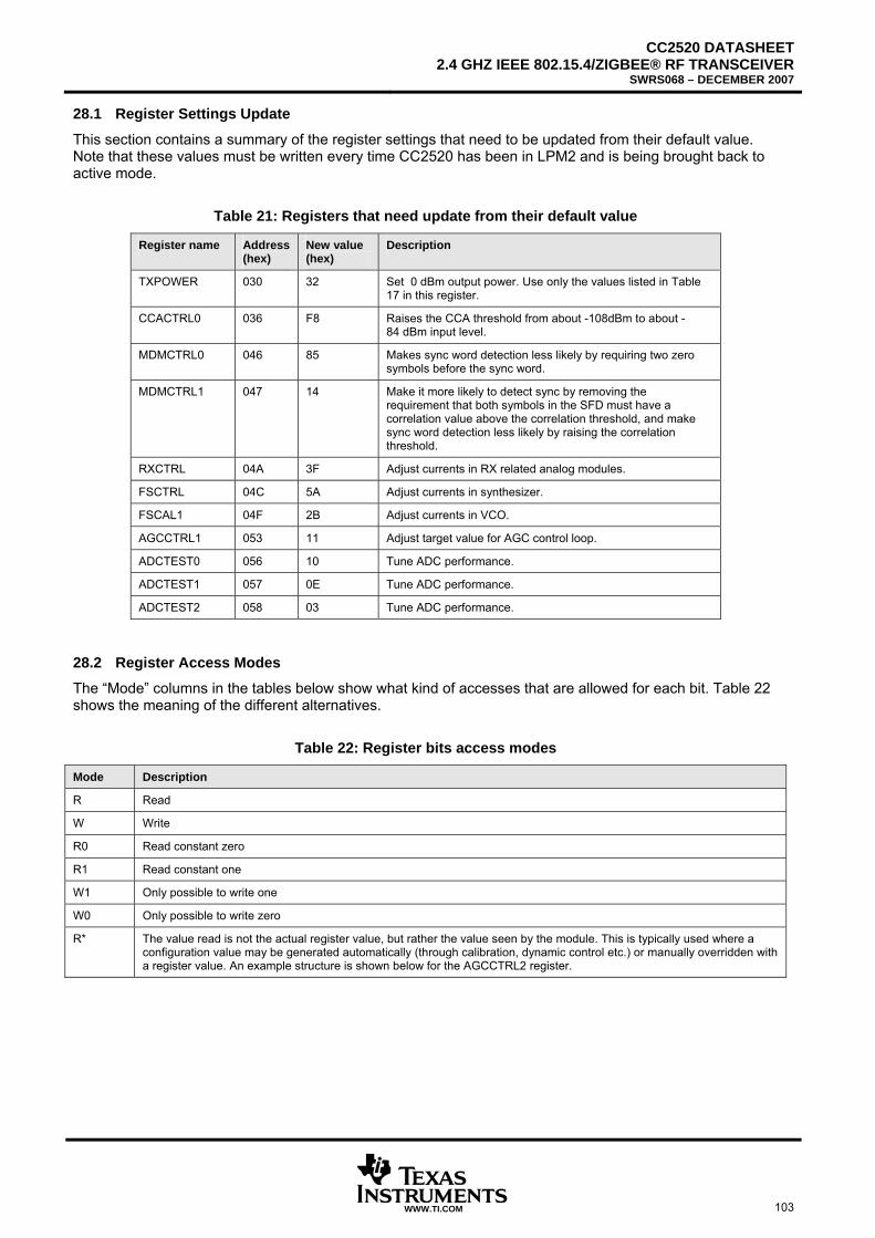
CC2520 DATASHEET2.4 GHZ IEEE 802.15.4/ZIGBEE® RF TRANSCEIVER
SWRS068 – DECEMBER 2007
WWW.TI.COM 103
28.1 Register Settings Update
This section contains a summary of the register settings that need to be updated from their default value. Note that these values must be written every time CC2520 has been in LPM2 and is being brought back to active mode.
Table 21: Registers that need update from their default value
Register name Address (hex)
New value (hex)
Description
TXPOWER 030 32 Set 0 dBm output power. Use only the values listed in Table 17 in this register.
CCACTRL0 036 F8 Raises the CCA threshold from about -108dBm to about -84 dBm input level.
MDMCTRL0 046 85 Makes sync word detection less likely by requiring two zero symbols before the sync word.
MDMCTRL1 047 14 Make it more likely to detect sync by removing the requirement that both symbols in the SFD must have a correlation value above the correlation threshold, and make sync word detection less likely by raising the correlation threshold.
RXCTRL 04A 3F Adjust currents in RX related analog modules.
FSCTRL 04C 5A Adjust currents in synthesizer.
FSCAL1 04F 2B Adjust currents in VCO.
AGCCTRL1 053 11 Adjust target value for AGC control loop.
ADCTEST0 056 10 Tune ADC performance.
ADCTEST1 057 0E Tune ADC performance.
ADCTEST2 058 03 Tune ADC performance.
28.2 Register Access Modes
The “Mode” columns in the tables below show what kind of accesses that are allowed for each bit. Table 22 shows the meaning of the different alternatives.
Table 22: Register bits access modes
Mode Description
R Read
W Write
R0 Read constant zero
R1 Read constant one
W1 Only possible to write one
W0 Only possible to write zero
R* The value read is not the actual register value, but rather the value seen by the module. This is typically used where a configuration value may be generated automatically (through calibration, dynamic control etc.) or manually overridden with a register value. An example structure is shown below for the AGCCTRL2 register.
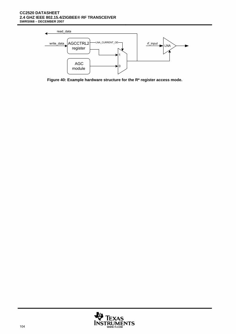
CC2520 DATASHEET 2.4 GHZ IEEE 802.15.4/ZIGBEE® RF TRANSCEIVER SWRS068 – DECEMBER 2007
104 WWW.TI.COM
AGCCTRL2register
LNA
AGCmodule
LNA_CURRENT_OE
1
0
rf_input
read_data
write_data
Figure 40: Example hardware structure for the R* register access mode.
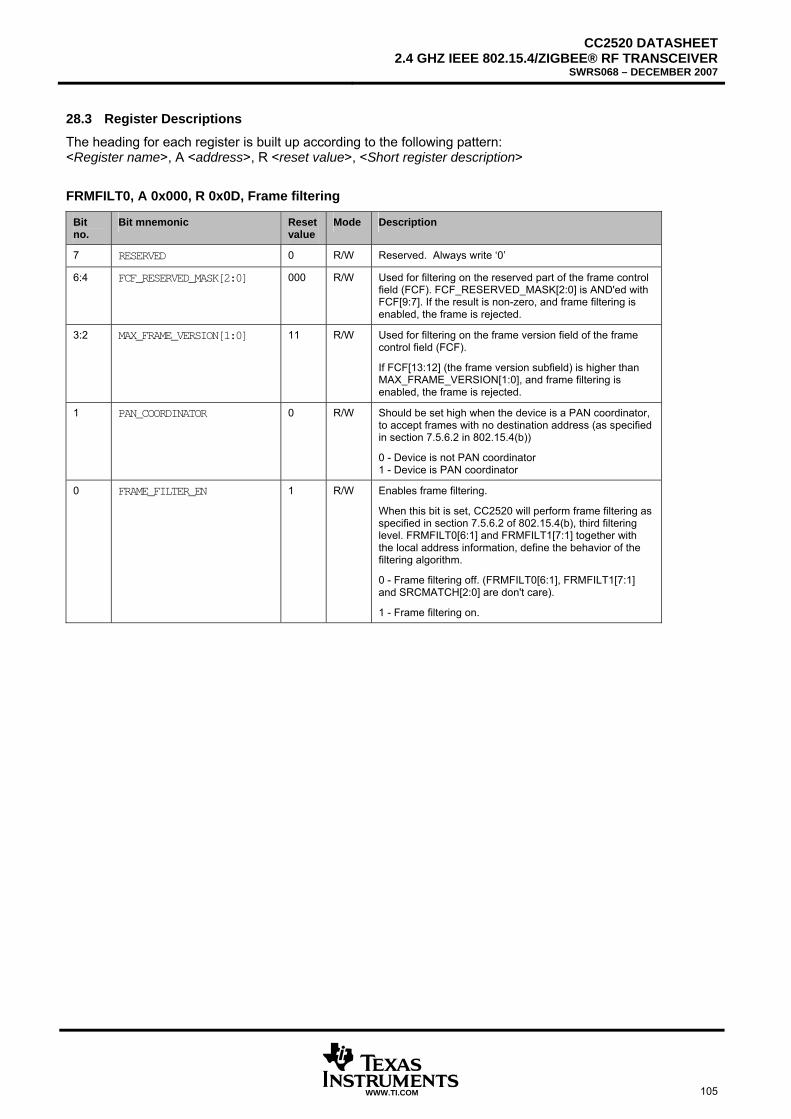
CC2520 DATASHEET2.4 GHZ IEEE 802.15.4/ZIGBEE® RF TRANSCEIVER
SWRS068 – DECEMBER 2007
WWW.TI.COM 105
28.3 Register Descriptions
The heading for each register is built up according to the following pattern: <Register name>, A <address>, R <reset value>, <Short register description>
FRMFILT0, A 0x000, R 0x0D, Frame filtering
Bit no.
Bit mnemonic Reset value
Mode Description
7 RESERVED 0 R/W Reserved. Always write ‘0’
6:4 FCF_RESERVED_MASK[2:0] 000 R/W Used for filtering on the reserved part of the frame control field (FCF). FCF_RESERVED_MASK[2:0] is AND'ed with FCF[9:7]. If the result is non-zero, and frame filtering is enabled, the frame is rejected.
3:2 MAX_FRAME_VERSION[1:0] 11 R/W Used for filtering on the frame version field of the frame control field (FCF).
If FCF[13:12] (the frame version subfield) is higher than MAX_FRAME_VERSION[1:0], and frame filtering is enabled, the frame is rejected.
1 PAN_COORDINATOR 0 R/W Should be set high when the device is a PAN coordinator, to accept frames with no destination address (as specified in section 7.5.6.2 in 802.15.4(b))
0 - Device is not PAN coordinator 1 - Device is PAN coordinator
0 FRAME_FILTER_EN 1 R/W Enables frame filtering.
When this bit is set, CC2520 will perform frame filtering as specified in section 7.5.6.2 of 802.15.4(b), third filtering level. FRMFILT0[6:1] and FRMFILT1[7:1] together with the local address information, define the behavior of the filtering algorithm.
0 - Frame filtering off. (FRMFILT0[6:1], FRMFILT1[7:1] and SRCMATCH[2:0] are don't care).
1 - Frame filtering on.
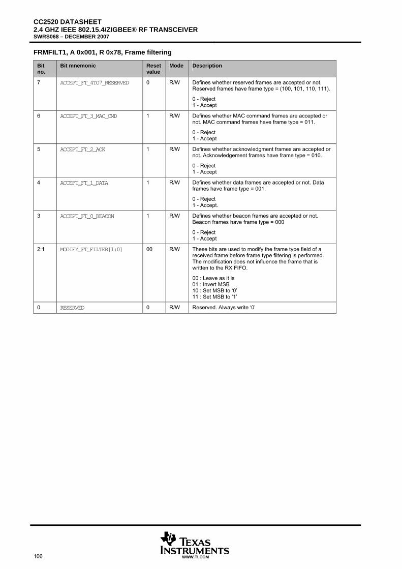
CC2520 DATASHEET 2.4 GHZ IEEE 802.15.4/ZIGBEE® RF TRANSCEIVER SWRS068 – DECEMBER 2007
106 WWW.TI.COM
FRMFILT1, A 0x001, R 0x78, Frame filtering
Bit no.
Bit mnemonic Reset value
Mode Description
7 ACCEPT_FT_4TO7_RESERVED 0 R/W Defines whether reserved frames are accepted or not. Reserved frames have frame type = (100, 101, 110, 111).
0 - Reject 1 - Accept
6 ACCEPT_FT_3_MAC_CMD 1 R/W Defines whether MAC command frames are accepted or not. MAC command frames have frame type = 011.
0 - Reject 1 - Accept
5 ACCEPT_FT_2_ACK 1 R/W Defines whether acknowledgment frames are accepted or not. Acknowledgement frames have frame type = 010.
0 - Reject 1 - Accept
4 ACCEPT_FT_1_DATA 1 R/W Defines whether data frames are accepted or not. Data frames have frame type = 001.
0 - Reject 1 - Accept.
3 ACCEPT_FT_0_BEACON 1 R/W Defines whether beacon frames are accepted or not. Beacon frames have frame type = 000
0 - Reject 1 - Accept
2:1 MODIFY_FT_FILTER[1:0] 00 R/W These bits are used to modify the frame type field of a received frame before frame type filtering is performed. The modification does not influence the frame that is written to the RX FIFO.
00 : Leave as it is 01 : Invert MSB 10 : Set MSB to ‘0’ 11 : Set MSB to ‘1’
0 RESERVED 0 R/W Reserved. Always write ‘0’
CC2520 DATASHEET2.4 GHZ IEEE 802.15.4/ZIGBEE® RF TRANSCEIVER
SWRS068 – DECEMBER 2007
WWW.TI.COM 107
SRCMATCH, A 0x002, R 0x07, Source address matching and pending bits
Bit no. Bit mnemonic Reset value
Mode Description
7:3 RESERVED[4:0] 0x00 R/W Reserved. Always write ‘0’
2 PEND_DATAREQ_ONLY 1 R/W When this bit is set, the AUTOPEND function also requires that the received frame is a "DATA REQUEST" MAC command frame.
1 AUTOPEND 1 R/W Automatic acknowledgment pending flag enable.
Upon reception of a frame, the pending bit in the (possibly) returned acknowledgment will be set automatically, given that:
- FRMFILT0.FRAME_FILTER_EN is set.
- SRCMATCH.SRC_MATCH_EN is set.
- SRCMATCH.AUTOPEND is set.
- The received frame matches the current SRCMATCH.PEND_DATAREQ_ONLY setting.
- The received source address matches at least one source match table entry, which is enabled in both SHORT_ADDR_EN and SHORT_PEND_EN or EXT_ADDR_EN and EXT_PEND_EN.
Note: Details for SHORT_PEND_EN and EXT_PEND_EN is found in memory map description.
0 SRC_MATCH_EN 1 R/W Source address matching enable (This bit is “don’t care” if FRMFILT0.FRAME_FILTER_EN = 0)
SRCSHORTEN0, A 0x004, R 0x00, Short address matching
Bit no. Bit mnemonic Reset value
Mode Description
7:0 SHORT_ADDR_EN[7:0] 0x00 R/W The 7:0 part of the 24-bit word SHORT_ADDR_EN that enables / disables source address matching for each of the 24 short address table entries.
Optional safety feature: To ensure that an entry in the source matching table is not used while it is being updated, set the corresponding SHORT_ADDR_EN bit to 0 while updating.
SRCSHORTEN1, A 0x005, R 0x00, Short address matching
Bit no. Bit mnemonic Reset value
Mode Description
7:0 SHORT_ADDR_EN[15:8] 0x00 R/W The 15:8 part of the 24-bit word SHORT_ADDR_EN See description of SRCSHORTEN0.
SRCSHORTEN2, A 0x006, R 0x00, Short address matching
Bit no. Bit mnemonic Reset value
Mode Description
7:0 SHORT_ADDR_EN[23:16] 0x00 R/W The 23:16 part of the 24-bit word SHORT_ADDR_EN See description of SRCSHORTEN0.
CC2520 DATASHEET 2.4 GHZ IEEE 802.15.4/ZIGBEE® RF TRANSCEIVER SWRS068 – DECEMBER 2007
108 WWW.TI.COM
SRCEXTEN0, A 0x008, R 0x00, Extended address matching
Bit no. Bit mnemonic Reset value
Mode Description
7:0 EXT_ADDR_EN[7:0] 0x00 R/W RO
The 7:0 part of the 24-bit word EXT_ADDR_EN that enables / disables source address matching for each of the 12 extended address table entries.
Write access: Extended address enable for table entry n (0 to 7) is mapped to EXT_ADDR_EN[2n]. All EXT_ADDR_EN[2n + 1] bits are read only and don’t care when written to.
Read access: Extended address enable for table entry n (0 to 7) is mapped to both EXT_ADDR_EN[2n] and EXT_ADDR_EN[2n+1].
Optional safety feature: To ensure that an entry in the source matching table is not used while it is being updated, set the corresponding EXT_ADDR_EN bit to 0 while updating.
SRCEXTEN1, A 0x009, R 0x00, Extended address matching
Bit no. Bit mnemonic Reset value
Mode Description
7:0 EXT_ADDR_EN[15:8] 0x00 R/W The 15:8 part of the 24-bit word EXT_ADDR_EN See description of SRCEXTEN0.
SRCEXTEN2, A 0x00A, R 0x00, Extended address matching
Bit no. Bit mnemonic Reset value
Mode Description
7:0 EXT_ADDR_EN[23:16] 0x00 R/W The 23:16 part of the 24-bit word EXT_ADDR_EN See description of SRCEXTEN0.
CC2520 DATASHEET2.4 GHZ IEEE 802.15.4/ZIGBEE® RF TRANSCEIVER
SWRS068 – DECEMBER 2007
WWW.TI.COM 109
FRMCTRL0, A 0x00C, R 0x40, Frame handling
Bit no. Bit mnemonic Reset value
Mode Description
7 APPEND_DATA_MODE 0 R/W When AUTOCRC = 0:Don’t care
When AUTOCRC = 1:
0: RSSI + The crc_ok bit and the 7 bit correlation value is appended at the end of each received frame
1: RSSI + The crc_ok bit and the 7 bit SRCRESINDEX is appended at the end of each received frame. See Table 15 for details.
6 AUTOCRC 1 R/W In TX: 1: A CRC-16 (ITU-T) is generated in hardware and appended to the transmitted frame. There is no need to write the two last bytes to TXBUF. 0: No CRC-16 is appended to the frame. The two last bytes of the frame must be generated manually and written to TXBUF (if not, TX_UNDERFLOW will occur).
In RX 1: The CRC-16 is checked in hardware, and replaced in the RX FIFO by a 16-bit status word which contains a CRC OK bit. The status word is controllable through APPEND_DATA_MODE 0: The last two bytes of the frame (crc-16 field) are stored in the RXFIFO. The CRC check (if any) must be done manually.
Note that this setting does not influence acknowledgment transmission (including AUTOACK)
5 AUTOACK 0 R/W Defines whether CC2520 automatically transmits acknowledge frames or not. When autoack is enabled, all frames that are accepted by address filtering, have the acknowledge request flag set and have a valid CRC, are automatically acknowledged 12 symbol periods after being received.
0 - Autoack disabled 1 - Autoack enabled
4 ENERGY_SCAN 0 R/W Defines whether the RSSI register contains the most recent signal strength or the peak signal strength since the energy scan was enabled.
0 - Most recent signal strength 1 - Peak signal strength
3:2 RX_MODE[1:0] 00 R/W Set RX modes
00: Normal operation, use RXFIFO. 01: Reserved 10: RXFIFO looping ignore overflow in RXFIFO, infinite reception.11: Same as normal operation except that symbol search is disabled. Can be used for RSSI or CCA measurements when it is undesired to find symbol.
1:0 TX_MODE[1:0] 00 R/W Set test modes for TX
00: Normal operation, transmit TXFIFO 01: Reserved. Should not be used. 10: TXFIFO looping ignore underflow in TXFIFO and read cyclic, infinite transmission. 11: Send pseudo random data from CRC, infinite transmission.
CC2520 DATASHEET 2.4 GHZ IEEE 802.15.4/ZIGBEE® RF TRANSCEIVER SWRS068 – DECEMBER 2007
110 WWW.TI.COM
FRMCTRL1, A 0x00D, R 0x01, Frame handling
Bit no.
Bit mnemonic Reset value
Mode Description
7:3 RESERVED 0x00 R0 Read as zero
2 PENDING_OR 0 R/W Defines whether the pending data bit in outgoing acknowledgment frames are always set to ‘1’ or controlled by the main FSM and the address filtering.
0 - Pending data bit is controlled by main FSM and address filtering 1 - Pending data bit is always ‘1’.
1 IGNORE_TX_UNDERF 0 R/W Defines whether TX underflow should be ignored or not.
0 - Normal TX operation. TX underflow is detected and TX is aborted if underflow occurs
1 - Ignore TX underflow. Transmit the number of bytes given by the length field.
0 SET_RXENMASK_ON_TX 1 R/W Defines whether STXON will set bit 14 in the RXENABLE register or leave it unchanged.
0: Do not affect RXENABLE.
1: Set bit 14 in RXENABLE. Used for backwards compatibility with CC2420.
CC2520 DATASHEET2.4 GHZ IEEE 802.15.4/ZIGBEE® RF TRANSCEIVER
SWRS068 – DECEMBER 2007
WWW.TI.COM 111
RXENABLE0, A 0x00E, R 0x00, RX enabling
Bit no.
Bit mnemonic Reset value
Mode Description
7:0 RXENMASK[7:0] 0x00 R/W LSB part of the 16 bit word RXENMASK
RXENABLE enables the receiver. A non-zero value in this register will cause the main FSM to enable the receiver when in idle, after transmission and after acknowledgement transmission.
The following strobes can modify RXENMASK:
SRXON: Set bit 15 in RXENMASK
STXON: Set bit 14 in RXENMASK if SET_RXENMASK_ON_TX = ‘1’
SRFOFF: Clears all bits in RXENMASK
The following instructions modifies RXENMASK:
RXMASKAND : Performs a bitwise AND between RXENMASK and the 16 bit parameter given with the instruction
RXMASKOR : Performs a bitwise OR between RXENMASK and the 16 bit parameter given with the instruction
RXENABLE can also be written and is bit accessible. BSET and BCLR set and clear any of the 16 bits in RXENMASK. SRXMASKBITSET and SRXMASKBITCLR will set and clear bit 13 in RXENMASK.
There are several sources which might try to modify RXENMASK simultaneously. To handle the case of simultaneous access to RXENMASK from different sources the following rules apply:
- If two sources are not in conflict (they modify different parts of the register) both their requests to modify RXENMASK will be processed.
-Data bus has priority over all sources (BSET, BCLR, REGWR, MEMWR)
Strobes which modify RXENMASK are prioritized as following:
1 SRFOFF
2 SXTON
3 SRXON
4 RXMASKOR
5 RXMASKAND
6 SRXMASKBITSET
7 SRXMASKBITCLR
RXENABLE1, A 0x00F, R 0x00, RX enabling
Bit no.
Bit mnemonic Reset value
Mode Description
7:0 RXENMASK[15:8] 0x00 R/W MSB part of the 16 bit word RXENMASK Se description of RXENABLE0.
CC2520 DATASHEET 2.4 GHZ IEEE 802.15.4/ZIGBEE® RF TRANSCEIVER SWRS068 – DECEMBER 2007
112 WWW.TI.COM
EXCFLAG0, A 0x010, R 0x00, Exception flags
Bit no.
Bit mnemonic Reset value
Mode Description
7:0 EXCFLAG[7:0] 0x00 R/W0 Exception pending bits for exceptions 7 to 0. Whenever an exception occurs this bit will be set by hardware. Only software can clear this bit. EXCFKLAG is write zero only and attempts to write ‘1’ to any bits in EXFLAG will not result in a register change.
1: This exception has occurred and not yet cleared. 0: This exception has not yet occurred or has been cleared by software.
Bit no Exception
0 RF_IDLE
1 TX_FRM_DONE
2 TX_ACK_DONE
3 TX_UNDERFLOW
4 TX_OVERFLOW
5 RX_UNDERFLOW
6 RX_OVERFLOW
7 RXENABLE_ZERO
EXCFLAG1, A 0x011, R 0x00, Exception flags
Bit no.
Bit mnemonic Reset value
Mode Description
7:0 EXCFLAG[15:8] 0x00 R/W0 Exception pending bits for exceptions 15 to 8. See description above.
Bit no Exception
8 RX_FRM_DONE
9 RX_FRM_ACCEPTED
10 SRC_MATCH_DONE
11 SRC_MATCH_FOUND
12 FIFOP
13 SFD
14 DPU_DONE_L
15 DPU_DONE_H
CC2520 DATASHEET2.4 GHZ IEEE 802.15.4/ZIGBEE® RF TRANSCEIVER
SWRS068 – DECEMBER 2007
WWW.TI.COM 113
EXCFLAG2, A 0x012, R 0x00, Exception flags
Bit no.
Bit mnemonic Reset value
Mode Description
7:0 EXCFLAG[23:16] 0x00 R/W0 Exception pending bits for exceptions 23 to 16. See description above.
Bit no Exception
16 MEMADDR_ERROR
17 USAGE_ERROR
18 OPERAND_ERROR
19 SPI_ERROR
20 RF_NO_LOCK
21 RX_FRM_ABORTED
22 RXBUFMOV_TIMEOUT
23 UNUSED
EXCMASKA0, A 0x014, R 0x00, Exception masking channel A
Bit no.
Bit mnemonic Reset value
Mode Description
7:0 EXCMASKA[7:0] 0x00 R/W The 7:0 part of 24 bit word EXCMASKA
Mask exceptions for channel A. If channel A is selected as output configuration for a pin, an exception indication will be generated on that pin when a selected exception occurs. If the complementary channel is selected, then an exception will be indicated when a masked exception occurs.
For each bit:
1: Selected 0: Masked
EXCMASKA1, A 0x015, R 0x00, Exception masking channel A
Bit no.
Bit mnemonic Reset value
Mode Description
7:0 EXCMASKA[15:8] 0x00 R/W The 15:8 part of 24 bit word EXCMASKA See description of EXCMASKA0.
EXCMASKA2, A 0x016, R 0x00, Exception masking channel A
Bit no.
Bit mnemonic Reset value
Mode Description
7:0 EXCMASKA[23:16] 0x00 R/W The 23:16 part of 24 bit word EXCMASKA See description of EXCMASKA0.
CC2520 DATASHEET 2.4 GHZ IEEE 802.15.4/ZIGBEE® RF TRANSCEIVER SWRS068 – DECEMBER 2007
114 WWW.TI.COM
EXCMASKB0, A 0x018, R 0x00, Exception masking channel B
Bit no.
Bit mnemonic Reset value
Mode Description
7:0 EXCMASKB[7:0] 0x00 R/W The 7:0 part of 24 bit word EXCMASKB
Mask exceptions for channel B. If channel B is selected as output configuration for a pin, an exception indication will be generated on that pin when a selected exception occurs. If the complementary channel is selected, then an exception will be indicated when a masked exception occurs.
For each bit:
1: Selected 0: Masked
EXCMASKB1, A 0x019, R 0x00, Exception masking channel B
Bit no.
Bit mnemonic Reset value
Mode Description
7:0 EXCMASKB[15:8] 0x00 R/W The 15:8 part of 24 bit word EXCMASKB See description of EXCMASKB0.
EXCMASKB2, A 0x01A, R 0x00, Exception masking channel B
Bit no.
Bit mnemonic Reset value
Mode Description
7:0 EXCMASKB[23:16] 0x00 R/W The 23:16 part of 24 bit word EXCMASKB See description of EXCMASKB0.
EXCBINDX0, A 0x01C, R 0x00, Exception binding channel X
Bit no.
Bit mnemonic Reset value
Mode Description
7:4 RESERVED 0x0 R0 Read as zero
3:0 INSTRUCTIONX 0x0 R/W Instruction for channel X
Instruction number to bind to exception. See documentation for GPIO configuration for list over possible instructions that can be bound.
EXCBINDX1, A 0x01D, R 0x12, Exception binding channel X
Bit no.
Bit mnemonic Reset value
Mode Description
7 BINDX_EN 0 R/W Defines whether exception binding for channel X is enabled or not.
0 - Binding disabled. 1 -: Binding enabled. Whenever the exception given by EXCEPTIONX occurs the instruction given by INSTRUCTIONX is executed.
6:5 RESERVED 00 R0 Read as zero
4:0 EXCEPTIONX 0x12 R/W Exception for channel X
Exception number to bind to an instruction. Se table in Exception overview for valid configurations
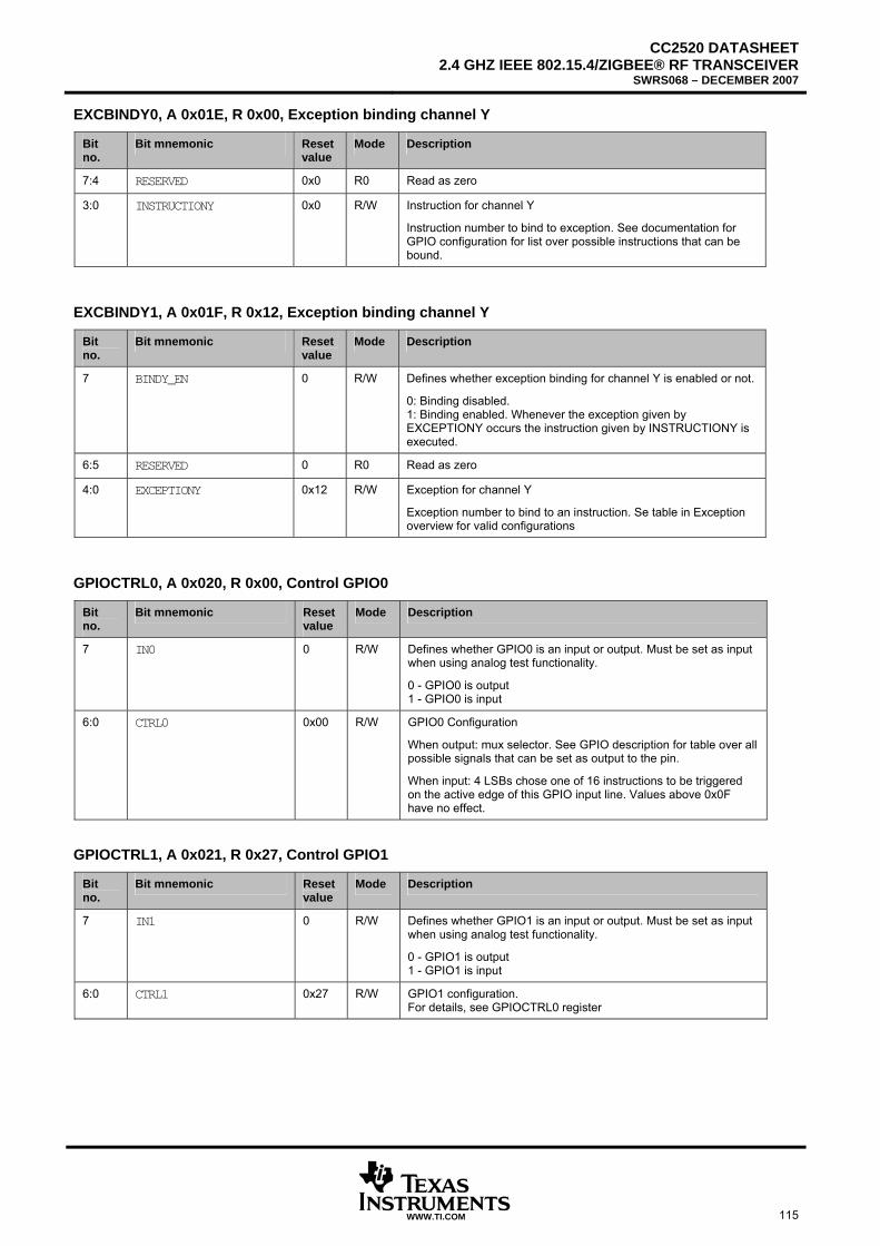
CC2520 DATASHEET2.4 GHZ IEEE 802.15.4/ZIGBEE® RF TRANSCEIVER
SWRS068 – DECEMBER 2007
WWW.TI.COM 115
EXCBINDY0, A 0x01E, R 0x00, Exception binding channel Y
Bit no.
Bit mnemonic Reset value
Mode Description
7:4 RESERVED 0x0 R0 Read as zero
3:0 INSTRUCTIONY 0x0 R/W Instruction for channel Y
Instruction number to bind to exception. See documentation for GPIO configuration for list over possible instructions that can be bound.
EXCBINDY1, A 0x01F, R 0x12, Exception binding channel Y
Bit no.
Bit mnemonic Reset value
Mode Description
7 BINDY_EN 0 R/W Defines whether exception binding for channel Y is enabled or not.
0: Binding disabled. 1: Binding enabled. Whenever the exception given by EXCEPTIONY occurs the instruction given by INSTRUCTIONY is executed.
6:5 RESERVED 0 R0 Read as zero
4:0 EXCEPTIONY 0x12 R/W Exception for channel Y
Exception number to bind to an instruction. Se table in Exception overview for valid configurations
GPIOCTRL0, A 0x020, R 0x00, Control GPIO0
Bit no.
Bit mnemonic Reset value
Mode Description
7 IN0 0 R/W Defines whether GPIO0 is an input or output. Must be set as input when using analog test functionality.
0 - GPIO0 is output 1 - GPIO0 is input
6:0 CTRL0 0x00 R/W GPIO0 Configuration
When output: mux selector. See GPIO description for table over all possible signals that can be set as output to the pin.
When input: 4 LSBs chose one of 16 instructions to be triggered on the active edge of this GPIO input line. Values above 0x0F have no effect.
GPIOCTRL1, A 0x021, R 0x27, Control GPIO1
Bit no.
Bit mnemonic Reset value
Mode Description
7 IN1 0 R/W Defines whether GPIO1 is an input or output. Must be set as input when using analog test functionality.
0 - GPIO1 is output 1 - GPIO1 is input
6:0 CTRL1 0x27 R/W GPIO1 configuration. For details, see GPIOCTRL0 register
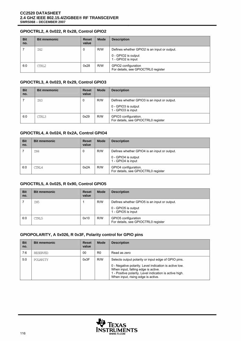
CC2520 DATASHEET 2.4 GHZ IEEE 802.15.4/ZIGBEE® RF TRANSCEIVER SWRS068 – DECEMBER 2007
116 WWW.TI.COM
GPIOCTRL2, A 0x022, R 0x28, Control GPIO2
Bit no.
Bit mnemonic Reset value
Mode Description
7 IN2 0 R/W Defines whether GPIO2 is an input or output.
0 - GPIO2 is output 1 - GPIO2 is input
6:0 CTRL2 0x28 R/W GPIO2 configuration For details, see GPIOCTRL0 register
GPIOCTRL3, A 0x023, R 0x29, Control GPIO3
Bit no.
Bit mnemonic Reset value
Mode Description
7 IN3 0 R/W Defines whether GPIO3 is an input or output.
0 - GPIO3 is output 1 - GPIO3 is input
6:0 CTRL3 0x29 R/W GPIO3 configuration. For details, see GPIOCTRL0 register
GPIOCTRL4, A 0x024, R 0x2A, Control GPIO4
Bit no.
Bit mnemonic Reset value
Mode Description
7 IN4 0 R/W Defines whether GPIO4 is an input or output.
0 - GPIO4 is output 1 - GPIO4 is input
6:0 CTRL4 0x2A R/W GPIO4 configuration. For details, see GPIOCTRL0 register
GPIOCTRL5, A 0x025, R 0x90, Control GPIO5
Bit no.
Bit mnemonic Reset value
Mode Description
7 IN5 1 R/W Defines whether GPIO5 is an input or output.
0 - GPIO5 is output 1 - GPIO5 is input
6:0 CTRL5 0x10 R/W GPIO5 configuration For details, see GPIOCTRL0 register
GPIOPOLARITY, A 0x026, R 0x3F, Polarity control for GPIO pins
Bit no.
Bit mnemonic Reset value
Mode Description
7:6 RESERVED 00 R0 Read as zero
5:0 POLARITY 0x3F R/W Selects output polarity or input edge of GPIO pins.
0 - Negative polarity. Level indication is active low. When input, falling edge is active. 1 - Positive polarity. Level indication is active high. When input, rising edge is active.
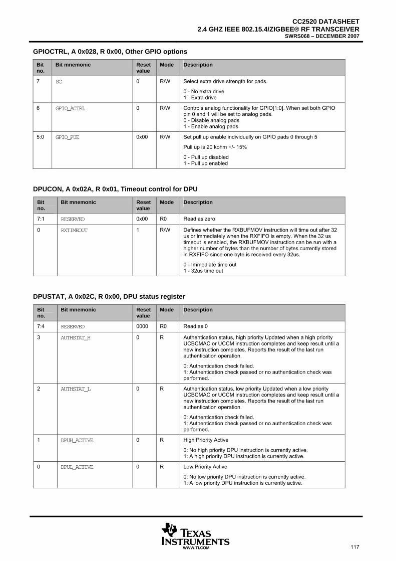
CC2520 DATASHEET2.4 GHZ IEEE 802.15.4/ZIGBEE® RF TRANSCEIVER
SWRS068 – DECEMBER 2007
WWW.TI.COM 117
GPIOCTRL, A 0x028, R 0x00, Other GPIO options
Bit no.
Bit mnemonic Reset value
Mode Description
7 SC 0 R/W Select extra drive strength for pads.
0 - No extra drive 1 - Extra drive
6 GPIO_ACTRL 0 R/W Controls analog functionality for GPIO[1:0]. When set both GPIO pin 0 and 1 will be set to analog pads. 0 - Disable analog pads 1 - Enable analog pads
5:0 GPIO_PUE 0x00 R/W Set pull up enable individually on GPIO pads 0 through 5
Pull up is 20 kohm +/- 15%
0 - Pull up disabled 1 - Pull up enabled
DPUCON, A 0x02A, R 0x01, Timeout control for DPU
Bit no.
Bit mnemonic Reset value
Mode Description
7:1 RESERVED 0x00 R0 Read as zero
0 RXTIMEOUT 1 R/W Defines whether the RXBUFMOV instruction will time out after 32 us or immediately when the RXFIFO is empty. When the 32 us timeout is enabled, the RXBUFMOV instruction can be run with a higher number of bytes than the number of bytes currently stored in RXFIFO since one byte is received every 32us.
0 - Immediate time out 1 - 32us time out
DPUSTAT, A 0x02C, R 0x00, DPU status register
Bit no.
Bit mnemonic Reset value
Mode Description
7:4 RESERVED 0000 R0 Read as 0
3 AUTHSTAT_H 0 R Authentication status, high priority Updated when a high priority UCBCMAC or UCCM instruction completes and keep result until a new instruction completes. Reports the result of the last run authentication operation.
0: Authentication check failed. 1: Authentication check passed or no authentication check was performed.
2 AUTHSTAT_L 0 R Authentication status, low priority Updated when a low priority UCBCMAC or UCCM instruction completes and keep result until a new instruction completes. Reports the result of the last run authentication operation.
0: Authentication check failed. 1: Authentication check passed or no authentication check was performed.
1 DPUH_ACTIVE 0 R High Priority Active
0: No high priority DPU instruction is currently active. 1: A high priority DPU instruction is currently active.
0 DPUL_ACTIVE 0 R Low Priority Active
0: No low priority DPU instruction is currently active. 1: A low priority DPU instruction is currently active.
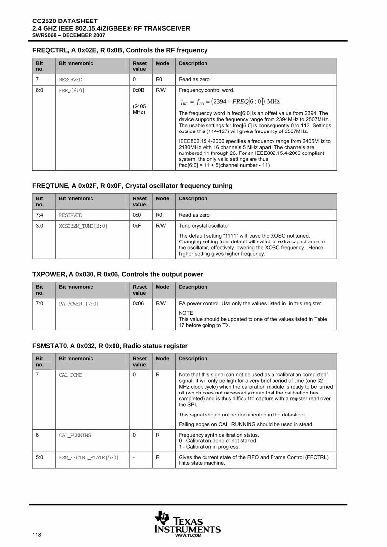
CC2520 DATASHEET 2.4 GHZ IEEE 802.15.4/ZIGBEE® RF TRANSCEIVER SWRS068 – DECEMBER 2007
118 WWW.TI.COM
FREQCTRL, A 0x02E, R 0x0B, Controls the RF frequency
Bit no.
Bit mnemonic Reset value
Mode Description
7 RESERVED 0 R0 Read as zero
6:0 FREQ[6:0] 0x0B
(2405 MHz)
R/W Frequency control word.
[ ]( ) MHz 0:62394 FREQff LORF +==
The frequency word in freq[6:0] is an offset value from 2394. The device supports the frequency range from 2394MHz to 2507MHz. The usable settings for freq[6:0] is consequently 0 to 113. Settings outside this (114-127) will give a frequency of 2507MHz.
IEEE802.15.4-2006 specifies a frequency range from 2405MHz to 2480MHz with 16 channels 5 MHz apart. The channels are numbered 11 through 26. For an IEEE802.15.4-2006 compliant system, the only valid settings are thus freq[6:0] = 11 + 5(channel number - 11)
FREQTUNE, A 0x02F, R 0x0F, Crystal oscillator frequency tuning
Bit no.
Bit mnemonic Reset value
Mode Description
7:4 RESERVED 0x0 R0 Read as zero
3:0 XOSC32M_TUNE[3:0] 0xF R/W Tune crystal oscillator
The default setting “1111” will leave the XOSC not tuned. Changing setting from default will switch in extra capacitance to the oscillator, effectively lowering the XOSC frequency. Hence higher setting gives higher frequency.
TXPOWER, A 0x030, R 0x06, Controls the output power
Bit no.
Bit mnemonic Reset value
Mode Description
7:0 PA_POWER [7:0] 0x06 R/W PA power control. Use only the values listed in in this register.
NOTE This value should be updated to one of the values listed in Table 17 before going to TX.
FSMSTAT0, A 0x032, R 0x00, Radio status register
Bit no.
Bit mnemonic Reset value
Mode Description
7 CAL_DONE 0 R Note that this signal can not be used as a “calibration completed” signal. It will only be high for a very brief period of time (one 32 MHz clock cycle) when the calibration module is ready to be turned off (which does not necessarily mean that the calibration has completed) and is thus difficult to capture with a register read over the SPI.
This signal should not be documented in the datasheet.
Falling edges on CAL_RUNNING should be used in stead.
6 CAL_RUNNING 0 R Frequency synth calibration status. 0 - Calibration done or not started 1 - Calibration in progress.
5:0 FSM_FFCTRL_STATE[5:0] - R Gives the current state of the FIFO and Frame Control (FFCTRL) finite state machine.
CC2520 DATASHEET2.4 GHZ IEEE 802.15.4/ZIGBEE® RF TRANSCEIVER
SWRS068 – DECEMBER 2007
WWW.TI.COM 119
FSMSTAT1, A 0x033, R 0x00, Radio status register
Bit no.
Bit mnemonic Reset value
Mode Description
7 FIFO 0 R FIFO is high whenever there is data in the RXFIFO. Low during RXFIFO overflow
6 FIFOP 0 R FIFOP is set high when there are more than FIFOP_THR bytes of data in the RXFIFO that has passed frame filtering.
FIFOP is set high when there is at least one complete frame in the RXFIFO. FIFOP is set low again when a byte is read from the RXFIFO and this leaves less than FIFOP_THR bytes in the FIFO.
FIFOP is high during RXFIFO overflow
5 SFD 0 R In TX: 0: When a complete frame with SFD has been sent or no SFD has been sent 1: SFD has been sent
In RX: 0: When a complete frame has been received or no SFD has been received 1: SFD has been received
4 CCA 0 R Clear channel assessment. Dependent on CCA_MODE settings. See CCACTRL1 for details.
3 SAMPLED_CCA 0 R Contains a sampled value of the CCA. The value is updated whenever a SSAMPLECCA or STXONCCA strobe is issued
2 LOCK_STATUS 0 R '1' when PLL is in lock, otherwise '0'.
1 TX_ACTIVE 0 R Status signal, active when FFCTRL is in one of the transmit states
0 RX_ACTIVE 0 R Status signal, active when FFCTRL is in one of the receive states
FIFOPCTRL, A 0x034, R 0x40, FIFOP threshold
Bit no.
Bit mnemonic Reset value
Mode Description
7 RESERVED 0 R0 Read as zero
6:0 FIFOP_THR[6:0] 0x40 R/W Threshold used when generating FIFOP signal
FSMCTRL, A 0x035, R 0x01, FSM options
Bit no.
Bit mnemonic Reset value
Mode Description
7:2 RESERVED 0x00 R0 Read as zero
1 SLOTTED_ACK 0 R/W Controls timing of transmission of acknowledge frames
0: The acknowledge frame will be sent 12 symbol periods after the end of the received frame which requests the aknowledge.
1: The acknowledge frame will be sent at the first backoff slot boundary more than 12 symbol periods after the end of the received frame which requests the aknowledge
0 RX2RX_TIME_OFF 1 R/W Defines whether or not a 12 symbol time out should be used after frame reception has ended.
0 - No time out. 1 - 12 symbol period time out.
CC2520 DATASHEET 2.4 GHZ IEEE 802.15.4/ZIGBEE® RF TRANSCEIVER SWRS068 – DECEMBER 2007
120 WWW.TI.COM
CCACTRL0, A 0x036, R 0xE0, CCA threshold
Bit no.
Bit mnemonic Reset value
Mode Description
7:0 CCA_THR[7:0] 0xE0 R/W Clear Channel Assessment threshold value, signed 2’s complement number for comparison with the RSSI.
The unit is 1 dB, offset is about 76dBm. The CCA signal goes high when the received signal is below this value. The CCA signal is available on the CCA pin and in FSMSTAT1 register.
Note that the value should never be set lower than CCA_HYST-128 in order to avoid erroneous behavior of the CCA signal.
NOTE The reset value translates to an input level of approximately -32 – 76 = -108 dBm, which is well below the sensitivity limit. That means the CCA signal will never indicate a clear channel.
This register should be updated to 0xF8, which translates to an input level of about -8 - 76 = -84dBm.
CCACTRL1, A 0x037, R 0x1A, Other CCA options
Bit no.
Bit mnemonic Reset value
Mode Description
7:5 RESERVED 000 R0 Read as zero
4:3 CCA_MODE[1:0] 11 R/W 00 : CCA always set to ‘1’ 01 : CCA = ‘1’ when RSSI < CCA_THR-CCA_HYST, CCA = ‘0’ when RSSI >= CCA_THR 10 : CCA = ‘1’ when not receiving a frame, else CCA = ‘0’ 11 : CCA = ‘1’ when RSSI < CCA_THR-CCA_HYST and not receiving a frame, CCA=0 when RSSI >= CCA_THR or receiving a frame
2:0 CCA_HYST[2:0] 010 R/W Sets the level of CCA hysteresis. Unsigned values given in dB.
RSSI, A 0x038, R 0x80, RSSI status register
Bit no.
Bit mnemonic Reset value
Mode Description
7:0 RSSI_VAL[7:0] 0x80 R RSSI estimate on a logarithmic scale, signed number on 2’s complement.
Unit is 1 dB, offset is TBD [depends on the absolute gain of the RX chain, including external components, and should be measured]. The RSSI value is averaged over 8 symbol periods. The RSSI_VALID status bit should be checked before reading RSSI_VAL the first time.
The reset value of –128 also indicates that the RSSI value is invalid.
RSSISTAT, A 0x039, R 0x00, RSSI valid status register
Bit no.
Bit mnemonic Reset value
Mode Description
7:1 RESERVED 0000 000
R0 Read as zero
0 RSSI_VALID 0 R RSSI value is valid. Occurs eight symbol periods after entering RX
CC2520 DATASHEET2.4 GHZ IEEE 802.15.4/ZIGBEE® RF TRANSCEIVER
SWRS068 – DECEMBER 2007
WWW.TI.COM 121
RXFIRST, A 0x03C, R 0x00, First byte in RXFIFO
Bit no.
Bit mnemonic Reset value
Mode Description
7:0 DATA[7:0] 0x00 R First byte of the RXFIFO. Note: Reading this register will not modify the contents of the FIFO.
RXFIFOCNT, A 0x03E, R 0x00, Number of bytes in RXFIFO
Bit no.
Bit mnemonic Reset value
Mode Description
7:0 RXFIFOCNT[7:0] 0x00 R Number of bytes in the RXFIFO. Unsigned integer.
TXFIFOCNT, A 0x03F, R 0x00, Number of bytes in TXFIFO
Bit no.
Bit mnemonic Reset value
Mode Description
7:0 TXFIFOCNT[7:0] 0x00 R Number of bytes in the TXFIFO. Unsigned integer.
CHIPID, A 0x040, R 0x84, Chip ID
Bit no.
Bit mnemonic Reset value
Mode Description
7:0 CHIPID[7:0] 0x84 R Chip ID number. 0x84 = CC2520
VERSION, A 0x042, R 0x00, Chip version number
Bit no.
Bit mnemonic Reset value
Mode Description
7:0 VERSION[7:0] 0x00 R Chip version. Unsigned integer.
CC2520 DATASHEET 2.4 GHZ IEEE 802.15.4/ZIGBEE® RF TRANSCEIVER SWRS068 – DECEMBER 2007
122 WWW.TI.COM
EXTCLOCK, A 0x044, R 0x20, Controls clock output
Bit no.
Bit mnemonic Reset value
Mode Description
7:6 RESERVED 00 R0 Read as zero
5 EXTCLOCK_EN 1 RW Defines whether the clock generator module for the external clock is enabled or not. Note that a GPIO pin must be configured as output and Clock must be selected in one of the GPIOCTRLn registers to get the clock at the selected pin.
1 - Clock running 0 - Clock off
4:0 EXT_FREQ 0x00 RW Frequency setting of external clock. Changes of frequencies are glitch free and have 50/50 duty cycle. I.e. a change of frequency will not have effect before a complete period of the current clock setting is finished.
Setting Div. factor Frequency [MHz]
00000 32 1,00
00001 31 1,03
00010 30 1,07
00011 29 1,10
00100 28 1,14
00101 27 1,19
00110 26 1,23
00111 25 1,28
01000 24 1,33
01001 23 1,39
01010 22 1,45
01011 21 1,52
01100 20 1,60
01101 19 1,68
01110 18 1,78
01111 17 1,88
10000 16 2,00
10001 15 2,13
10010 14 2,29
10011 13 2,46
10100 12 2,67
10101 11 2,91
10110 10 3,20
10111 9 3,56
11000 8 4,00
11001 7 4,57
11010 6 5,33
11011 5 6,40
11100 4 8,00
11101 3 10,67
11110 2 16,00
11111 2 16,00
CC2520 DATASHEET2.4 GHZ IEEE 802.15.4/ZIGBEE® RF TRANSCEIVER
SWRS068 – DECEMBER 2007
WWW.TI.COM 123
MDMCTRL0, A 0x046, R 0x45, Controls modem
Bit no.
Bit mnemonic Reset value
Mode Description
7:6 DEM_NUM_ZEROS[1:0] 01 R/W Sets how many zero symbols have to be detected before the sync word when searching for sync. Note that only one is required to have a correlation value above the correlation threshold set in MDMCTRL1 register.
00 : reserved 01 : 1 zero symbols 10 : 2 zero symbols 11 : 3 zero symbols
NOTE This value should be updated to “10” before attempting RX. Testing has shown that the reset value causes too many false frames to be received.
5 DEMOD_AVG_MODE 0 R/W Defines the behavior or the frequency offset averaging filter.
0 - Lock average level after preamble match. Restart frequency offset calibration when searching for the next frame. 1 - Continuously update average level.
4:1 PREAMBLE_LENGTH [3:0]
0010 R/W The number of preamble bytes (2 zero-symbols) to be sent in TX mode prior to the SFD, encoded in steps of 2. The reset value of 2 is compliant with IEEE 802.15.4
0000 - 2 leading zero bytes 0001 - 3 leading zero bytes 0010 - 4 leading zero bytes … 1111 - 17 leading zero bytes
0 TX_FILTER 1 R/W Defines what kind of TX filter that is used. The normal TX filter is as defined by the IEEE802.15.4 standard. Extra filtering may be applied in order to lower the out of band emissions.
0 - Normal TX filtering 1 - Enable extra filtering
MDMCTRL1, A 0x047, R 0x2E, Controls modem
Bit no.
Bit mnemonic Reset value
Mode Description
7:6 RESERVED 00 R0 Read as zero
5 CORR_THR_SFD 1 R/W Defines requirements for SFD detection:
0 - The correlation value of one of the zero symbols of the preamble must be above the correlation threshold. 1 - The correlation value of one zero symbol of the preamble and both symbols in the SFD must be above the correlation threshold.
NOTE This value should be changed to ‘0’ before attempting RX. This will give the best trade off between good sensitivity and few false SFD detections.
4:0 CORR_THR[4:0] 0x0E R/W Demodulator correlator threshold value, required before SFD search.
Threshold value adjusts how the receiver synchronizes to data from the radio. If threshold is set too low sync can more easily be found on noise. If set too high the sensitivity will be reduced but sync will not likely be found on noise.
I combination with DEM_NUM_ZEROS the system can be tuned so sensitivity is high with less synch found on noise.
NOTE This value should be changed to 0x14 before attempting RX. Testing has shown that too many false frames are received if the reset value is used.
CC2520 DATASHEET 2.4 GHZ IEEE 802.15.4/ZIGBEE® RF TRANSCEIVER SWRS068 – DECEMBER 2007
124 WWW.TI.COM
FREQEST, A 0x048, R 0x00, Estimated RF frequency offset.
Bit no.
Bit mnemonic Reset value
Mode Description
7:0 FREQEST[7:0] 0x00 R Signed 2’s complement value. Contains an estimate of the frequency offset between carrier and the receiver LO. The offset frequency is FREQESTx7800 Hz. DEM_AVG_MODE controls when this estimate is updated. If DEM_AVG_MODE = 0 it is updated until sync is found. Then the frequency offset estimate is frozen until the end of the received frame. If DEM_AVG_MODE = 1 it is updated as long as the demodulator is enabled.
MDMTEST1, A 0x05B, R 0x08, Test register for modem
Bit no.
Bit mnemonic Reset value
Mode Description
7:4 RESERVED 0000 R0 Read as zero
3 RESERVED 1 R/W Do not write.
2 RFC_SNIFF_EN 0 R/W 0 - Packet sniffer module disabled 1 - Packet sniffer module enabled. The received and transmitted data can be observed on GPIO pins.
1 MODULATION_MODE 0 R/W Set one of two RF modulation modes for RX / TX
0 - IEEE 802.15.4 compliant mode 1 - Reversed phase, non-IEEE compliant
0 RESERVED 0 R/W Do not write.
CC2520 DATASHEET2.4 GHZ IEEE 802.15.4/ZIGBEE® RF TRANSCEIVER
SWRS068 – DECEMBER 2007
WWW.TI.COM 125
The following registers in the address range 0x04A to 0x07F are for performance tuning and test purposes and should generally not be written. The registers that require updates to give the performance described in this datasheet are listed in Table 21: Registers that need update from their default value.
RXCTRL, A 0x04A, R 0x29, Test/tuning of RX modules
FSCTRL, A 0x04C, R 0x55, Test/tuning of synthesizer
FSCAL0, A 0x04E, R 0x24, Test/tuning of synthesizer
FSCAL1, A 0x04F, R 0x29, Test/tuning of VCO
FSCAL2, A 0x050, R 0x20, Test/tuning of VCO
FSCAL3, A 0x051, R 0x2A, Test/tuning of VCO
AGCCTRL0, A 0x052, R 0x5F, Test/tuning of AGC
AGCCTRL1, A 0x053, R 0x0E, Test/tuning of AGC
AGCCTRL2, A 0x054, R 0x00, Test/tuning of LNA
AGCCTRL3, A 0x055, R 0x2E, Test/tuning of AGC and AAF
ADCTEST0, A 0x056, R 0x66, Test/tuning of ADC
ADCTEST1, A 0x057, R 0x0A, Test/tuning of ADC
ADCTEST2, A 0x058, R 0x05, Test/tuning of ADC
MDMTEST0, A 0x05A, R 0x05, Test/tuning of modem
DACTEST0, A 0x05C, R 0x00, Test/tuning of DAC
DACTEST1, A 0x05D, R 0x00, Test/tuning of DAC
ATEST, A 0x05E, R 0x00, Controls analog test mode
DACTEST2, A 0x05F, R 0x00, Test/tuning of DAC
PTEST0, A 0x060, R 0x00, Test/tuning of power down signals
PTEST1, A 0x061, R 0x00, Test/tuning of power down signals
RESERVED, A 0x062, R 0x00, Not currently in use
DPUBIST, A 0x07A, R 0x00, Test/tuning of DPU ROM
ACTBIST, A 0x07C, R 0x00, Test/tuning of ACT ROM
RAMBIST, A 0x07E, R 0x02, Test/tuning of RAM

CC2520 DATASHEET 2.4 GHZ IEEE 802.15.4/ZIGBEE® RF TRANSCEIVER SWRS068 – DECEMBER 2007
126 WWW.TI.COM
29 Datasheet Revision History Literature Number
Release Date Comments
SWRS068 2007-12-20 Initial release
NOTE: Page and figure numbers refer to the respective document revision.
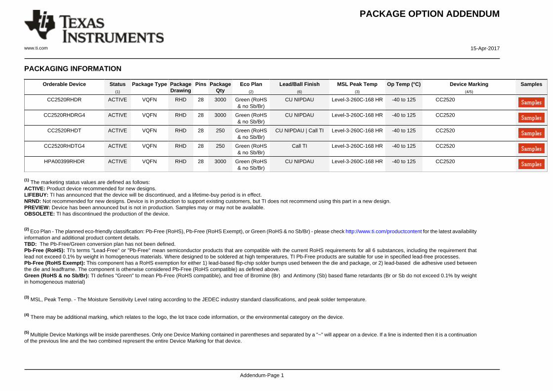
PACKAGE OPTION ADDENDUM
www.ti.com 15-Apr-2017
Addendum-Page 1
PACKAGING INFORMATION
Orderable Device Status(1)
Package Type PackageDrawing
Pins PackageQty
Eco Plan(2)
Lead/Ball Finish(6)
MSL Peak Temp(3)
Op Temp (°C) Device Marking(4/5)
Samples
CC2520RHDR ACTIVE VQFN RHD 28 3000 Green (RoHS& no Sb/Br)
CU NIPDAU Level-3-260C-168 HR -40 to 125 CC2520
CC2520RHDRG4 ACTIVE VQFN RHD 28 3000 Green (RoHS& no Sb/Br)
CU NIPDAU Level-3-260C-168 HR -40 to 125 CC2520
CC2520RHDT ACTIVE VQFN RHD 28 250 Green (RoHS& no Sb/Br)
CU NIPDAU | Call TI Level-3-260C-168 HR -40 to 125 CC2520
CC2520RHDTG4 ACTIVE VQFN RHD 28 250 Green (RoHS& no Sb/Br)
Call TI Level-3-260C-168 HR -40 to 125 CC2520
HPA00399RHDR ACTIVE VQFN RHD 28 3000 Green (RoHS& no Sb/Br)
CU NIPDAU Level-3-260C-168 HR -40 to 125 CC2520
(1) The marketing status values are defined as follows:ACTIVE: Product device recommended for new designs.LIFEBUY: TI has announced that the device will be discontinued, and a lifetime-buy period is in effect.NRND: Not recommended for new designs. Device is in production to support existing customers, but TI does not recommend using this part in a new design.PREVIEW: Device has been announced but is not in production. Samples may or may not be available.OBSOLETE: TI has discontinued the production of the device.
(2) Eco Plan - The planned eco-friendly classification: Pb-Free (RoHS), Pb-Free (RoHS Exempt), or Green (RoHS & no Sb/Br) - please check http://www.ti.com/productcontent for the latest availabilityinformation and additional product content details.TBD: The Pb-Free/Green conversion plan has not been defined.Pb-Free (RoHS): TI's terms "Lead-Free" or "Pb-Free" mean semiconductor products that are compatible with the current RoHS requirements for all 6 substances, including the requirement thatlead not exceed 0.1% by weight in homogeneous materials. Where designed to be soldered at high temperatures, TI Pb-Free products are suitable for use in specified lead-free processes.Pb-Free (RoHS Exempt): This component has a RoHS exemption for either 1) lead-based flip-chip solder bumps used between the die and package, or 2) lead-based die adhesive used betweenthe die and leadframe. The component is otherwise considered Pb-Free (RoHS compatible) as defined above.Green (RoHS & no Sb/Br): TI defines "Green" to mean Pb-Free (RoHS compatible), and free of Bromine (Br) and Antimony (Sb) based flame retardants (Br or Sb do not exceed 0.1% by weightin homogeneous material)
(3) MSL, Peak Temp. - The Moisture Sensitivity Level rating according to the JEDEC industry standard classifications, and peak solder temperature.
(4) There may be additional marking, which relates to the logo, the lot trace code information, or the environmental category on the device.
(5) Multiple Device Markings will be inside parentheses. Only one Device Marking contained in parentheses and separated by a "~" will appear on a device. If a line is indented then it is a continuationof the previous line and the two combined represent the entire Device Marking for that device.
PACKAGE OPTION ADDENDUM
www.ti.com 15-Apr-2017
Addendum-Page 2
(6) Lead/Ball Finish - Orderable Devices may have multiple material finish options. Finish options are separated by a vertical ruled line. Lead/Ball Finish values may wrap to two lines if the finishvalue exceeds the maximum column width.
Important Information and Disclaimer:The information provided on this page represents TI's knowledge and belief as of the date that it is provided. TI bases its knowledge and belief on informationprovided by third parties, and makes no representation or warranty as to the accuracy of such information. Efforts are underway to better integrate information from third parties. TI has taken andcontinues to take reasonable steps to provide representative and accurate information but may not have conducted destructive testing or chemical analysis on incoming materials and chemicals.TI and TI suppliers consider certain information to be proprietary, and thus CAS numbers and other limited information may not be available for release.
In no event shall TI's liability arising out of such information exceed the total purchase price of the TI part(s) at issue in this document sold by TI to Customer on an annual basis.
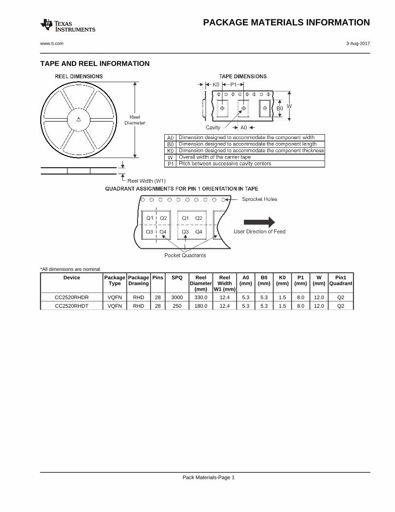
TAPE AND REEL INFORMATION
*All dimensions are nominal
Device PackageType
PackageDrawing
Pins SPQ ReelDiameter
(mm)
ReelWidth
W1 (mm)
A0(mm)
B0(mm)
K0(mm)
P1(mm)
W(mm)
Pin1Quadrant
CC2520RHDR VQFN RHD 28 3000 330.0 12.4 5.3 5.3 1.5 8.0 12.0 Q2
CC2520RHDT VQFN RHD 28 250 180.0 12.4 5.3 5.3 1.5 8.0 12.0 Q2
PACKAGE MATERIALS INFORMATION
www.ti.com 3-Aug-2017
Pack Materials-Page 1
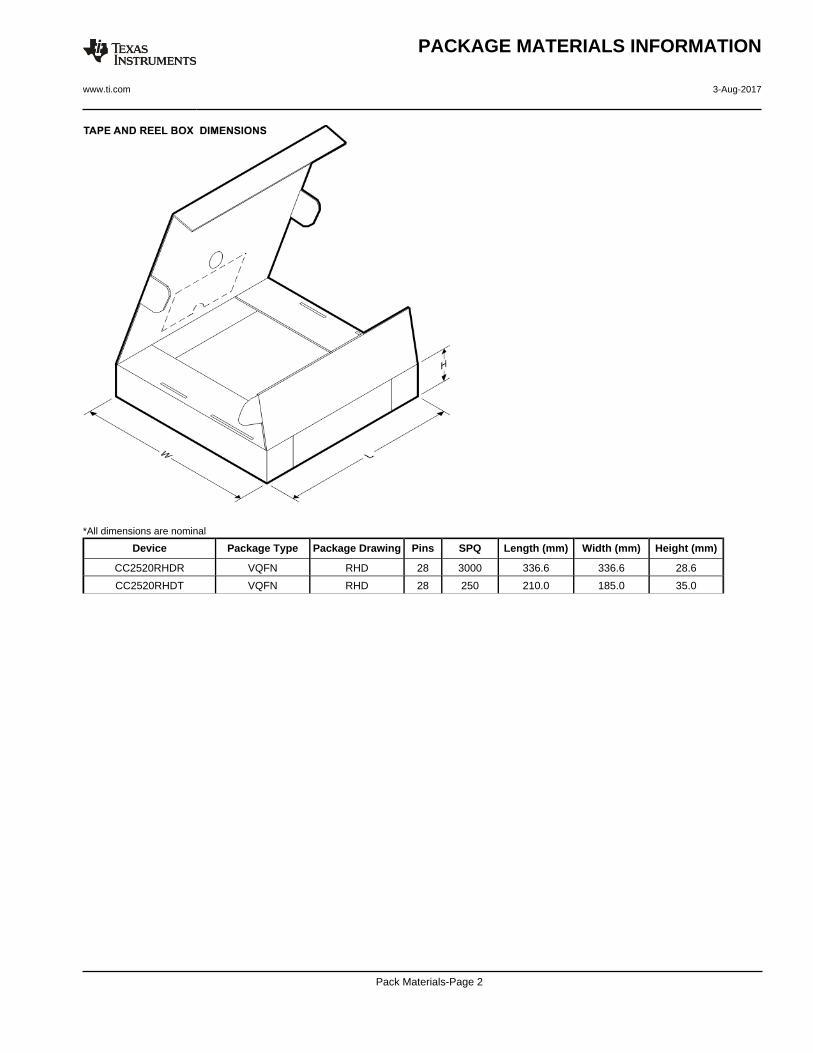
*All dimensions are nominal
Device Package Type Package Drawing Pins SPQ Length (mm) Width (mm) Height (mm)
CC2520RHDR VQFN RHD 28 3000 336.6 336.6 28.6
CC2520RHDT VQFN RHD 28 250 210.0 185.0 35.0
PACKAGE MATERIALS INFORMATION
www.ti.com 3-Aug-2017
Pack Materials-Page 2
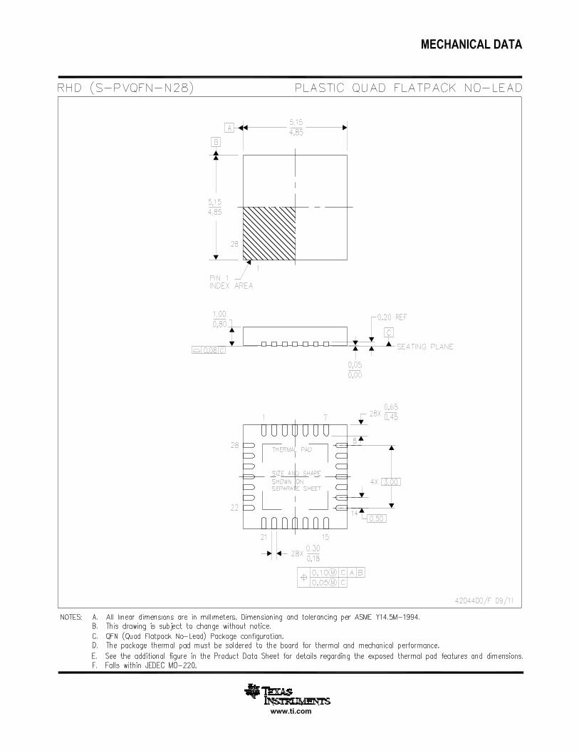

IMPORTANT NOTICE
Texas Instruments Incorporated (TI) reserves the right to make corrections, enhancements, improvements and other changes to itssemiconductor products and services per JESD46, latest issue, and to discontinue any product or service per JESD48, latest issue. Buyersshould obtain the latest relevant information before placing orders and should verify that such information is current and complete.TI’s published terms of sale for semiconductor products (http://www.ti.com/sc/docs/stdterms.htm) apply to the sale of packaged integratedcircuit products that TI has qualified and released to market. Additional terms may apply to the use or sale of other types of TI products andservices.Reproduction of significant portions of TI information in TI data sheets is permissible only if reproduction is without alteration and isaccompanied by all associated warranties, conditions, limitations, and notices. TI is not responsible or liable for such reproduceddocumentation. Information of third parties may be subject to additional restrictions. Resale of TI products or services with statementsdifferent from or beyond the parameters stated by TI for that product or service voids all express and any implied warranties for theassociated TI product or service and is an unfair and deceptive business practice. TI is not responsible or liable for any such statements.Buyers and others who are developing systems that incorporate TI products (collectively, “Designers”) understand and agree that Designersremain responsible for using their independent analysis, evaluation and judgment in designing their applications and that Designers havefull and exclusive responsibility to assure the safety of Designers' applications and compliance of their applications (and of all TI productsused in or for Designers’ applications) with all applicable regulations, laws and other applicable requirements. Designer represents that, withrespect to their applications, Designer has all the necessary expertise to create and implement safeguards that (1) anticipate dangerousconsequences of failures, (2) monitor failures and their consequences, and (3) lessen the likelihood of failures that might cause harm andtake appropriate actions. Designer agrees that prior to using or distributing any applications that include TI products, Designer willthoroughly test such applications and the functionality of such TI products as used in such applications.TI’s provision of technical, application or other design advice, quality characterization, reliability data or other services or information,including, but not limited to, reference designs and materials relating to evaluation modules, (collectively, “TI Resources”) are intended toassist designers who are developing applications that incorporate TI products; by downloading, accessing or using TI Resources in anyway, Designer (individually or, if Designer is acting on behalf of a company, Designer’s company) agrees to use any particular TI Resourcesolely for this purpose and subject to the terms of this Notice.TI’s provision of TI Resources does not expand or otherwise alter TI’s applicable published warranties or warranty disclaimers for TIproducts, and no additional obligations or liabilities arise from TI providing such TI Resources. TI reserves the right to make corrections,enhancements, improvements and other changes to its TI Resources. TI has not conducted any testing other than that specificallydescribed in the published documentation for a particular TI Resource.Designer is authorized to use, copy and modify any individual TI Resource only in connection with the development of applications thatinclude the TI product(s) identified in such TI Resource. NO OTHER LICENSE, EXPRESS OR IMPLIED, BY ESTOPPEL OR OTHERWISETO ANY OTHER TI INTELLECTUAL PROPERTY RIGHT, AND NO LICENSE TO ANY TECHNOLOGY OR INTELLECTUAL PROPERTYRIGHT OF TI OR ANY THIRD PARTY IS GRANTED HEREIN, including but not limited to any patent right, copyright, mask work right, orother intellectual property right relating to any combination, machine, or process in which TI products or services are used. Informationregarding or referencing third-party products or services does not constitute a license to use such products or services, or a warranty orendorsement thereof. Use of TI Resources may require a license from a third party under the patents or other intellectual property of thethird party, or a license from TI under the patents or other intellectual property of TI.TI RESOURCES ARE PROVIDED “AS IS” AND WITH ALL FAULTS. TI DISCLAIMS ALL OTHER WARRANTIES ORREPRESENTATIONS, EXPRESS OR IMPLIED, REGARDING RESOURCES OR USE THEREOF, INCLUDING BUT NOT LIMITED TOACCURACY OR COMPLETENESS, TITLE, ANY EPIDEMIC FAILURE WARRANTY AND ANY IMPLIED WARRANTIES OFMERCHANTABILITY, FITNESS FOR A PARTICULAR PURPOSE, AND NON-INFRINGEMENT OF ANY THIRD PARTY INTELLECTUALPROPERTY RIGHTS. TI SHALL NOT BE LIABLE FOR AND SHALL NOT DEFEND OR INDEMNIFY DESIGNER AGAINST ANY CLAIM,INCLUDING BUT NOT LIMITED TO ANY INFRINGEMENT CLAIM THAT RELATES TO OR IS BASED ON ANY COMBINATION OFPRODUCTS EVEN IF DESCRIBED IN TI RESOURCES OR OTHERWISE. IN NO EVENT SHALL TI BE LIABLE FOR ANY ACTUAL,DIRECT, SPECIAL, COLLATERAL, INDIRECT, PUNITIVE, INCIDENTAL, CONSEQUENTIAL OR EXEMPLARY DAMAGES INCONNECTION WITH OR ARISING OUT OF TI RESOURCES OR USE THEREOF, AND REGARDLESS OF WHETHER TI HAS BEENADVISED OF THE POSSIBILITY OF SUCH DAMAGES.Unless TI has explicitly designated an individual product as meeting the requirements of a particular industry standard (e.g., ISO/TS 16949and ISO 26262), TI is not responsible for any failure to meet such industry standard requirements.Where TI specifically promotes products as facilitating functional safety or as compliant with industry functional safety standards, suchproducts are intended to help enable customers to design and create their own applications that meet applicable functional safety standardsand requirements. Using products in an application does not by itself establish any safety features in the application. Designers mustensure compliance with safety-related requirements and standards applicable to their applications. Designer may not use any TI products inlife-critical medical equipment unless authorized officers of the parties have executed a special contract specifically governing such use.Life-critical medical equipment is medical equipment where failure of such equipment would cause serious bodily injury or death (e.g., lifesupport, pacemakers, defibrillators, heart pumps, neurostimulators, and implantables). Such equipment includes, without limitation, allmedical devices identified by the U.S. Food and Drug Administration as Class III devices and equivalent classifications outside the U.S.TI may expressly designate certain products as completing a particular qualification (e.g., Q100, Military Grade, or Enhanced Product).Designers agree that it has the necessary expertise to select the product with the appropriate qualification designation for their applicationsand that proper product selection is at Designers’ own risk. Designers are solely responsible for compliance with all legal and regulatoryrequirements in connection with such selection.Designer will fully indemnify TI and its representatives against any damages, costs, losses, and/or liabilities arising out of Designer’s non-compliance with the terms and provisions of this Notice.
Mailing Address: Texas Instruments, Post Office Box 655303, Dallas, Texas 75265Copyright © 2017, Texas Instruments Incorporated