
22 μA, RRIO, CMOS,18 V Operational Amplifiers Data …€¦ · Data Sheet AD8657/AD8659 Rev. C |...
24
22 μA, RRIO, CMOS,18 V Operational Amplifiers Data Sheet AD8657/AD8659 Rev. C Information furnished by Analog Devices is believed to be accurate and reliable. However, no responsibility is assumed by Analog Devices for its use, nor for any infringements of patents or other rights of third parties that may result from its use. Specifications subject to change without notice. No license is granted by implication or otherwise under any patent or patent rights of Analog Devices. Trademarks and registered trademarks are the property of their respective owners. One Technology Way, P.O. Box 9106, Norwood, MA 02062-9106, U.S.A. Tel: 781.329.4700 www.analog.com Fax: 781.461.3113 ©2011–2017 Analog Devices, Inc. All rights reserved. FEATURES Micropower at high voltage (18 V): 22 μA maximum Low offset voltage: 350 μV maximum Low input bias current: 20 pA maximum Gain bandwidth product: 230 kHz at AV = 100 typical Unity-gain crossover: 230 kHz −3 dB closed-loop bandwidth: 305 kHz Single-supply operation: 2.7 V to 18 V Dual-supply operation: ±1.35 V to ±9 V Unity-gain stable Excellent electromagnetic interference immunity APPLICATIONS Portable operating systems Current monitors 4 mA to 20 mA loop drivers Buffer/level shifting Multipole filters Remote/wireless sensors Low power transimpedance amplifiers GENERAL DESCRIPTION The AD8657/AD8659 are dual and quad micropower, precision, rail-to-rail input/output amplifiers optimized for low power and wide operating supply voltage range applications. The AD8657/AD8659 operate from 2.7 V to 18 V with a typical quiescent supply current of 18 μA. The devices use the Analog Devices, Inc., patented DigiTrim® trimming technique, which achieves low offset voltage. The AD8657/AD8659 also have high immunity to electromagnetic interference. The combination of low supply current, low offset voltage, very low input bias current, wide supply range, and rail-to-rail input and output make the AD8657/AD8659 ideal for current monitoring in process and motor control applications. The combination of precision specifications makes these devices ideal for dc gain and buffering of sensor front ends or high impedance input sources in wireless or remote sensors or transmitters. The AD8657/AD8659 are specified over the extended industrial temperature range (−40°C to +125°C). e AD8657 is available in an 8-lead MSOP package and an 8-lead LFCSP package; the AD8659 is available in a 14-lead SOIC package and 16-lead LFCSP package. PIN CONNECTION DIAGRAMS OUT A 1 –IN A 2 +IN A 3 V– 4 V+ 8 OUT B 7 –IN B 6 +IN B 5 AD8657 TOP VIEW (Not to Scale) 08804-001 Figure 1. AD8657 Pin Configuration, 8-Lead MSOP 08804-061 AD8657 TOP VIEW (Not to Scale) NOTES 1. CONNECT THE EXPOSED PAD TO V– OR LEAVE IT UNCONNECTED. 3 +IN A 4 V– 1 OUT A 2 –IN A 6 –IN B 5 +IN B 8 V+ 7 OUT B Figure 2. AD8657 Pin Configuration, 8-Lead LFCSP Note: For AD8659 pin connections and for more information about the pin connections for these products, see the Pin Configurations and Function Descriptions section. 0 10 20 30 40 50 60 –50 –25 0 25 50 75 100 125 I SY PER AMP (μA) TEMPERATURE (°C) V SY = 2.7V V SY = 18V 08804-023 Figure 3. AD8657, Supply Current vs. Temperature Table 1. Precision Micropower Op Amps (<250 μA) Supply Voltage 5 V 12 V to 16 V 36 V Single AD8538 OP196 AD8603 ADA4051-1 Dual AD8539 AD8657 AD8622 AD8607 ADA4091-2 ADA4051-2 ADA4096-2 Quad AD8609 AD8659 AD8624 ADA4091-4 ADA4096-4
Transcript of 22 μA, RRIO, CMOS,18 V Operational Amplifiers Data …€¦ · Data Sheet AD8657/AD8659 Rev. C |...
22 μA, RRIO, CMOS,18 V Operational Amplifiers
Data Sheet AD8657/AD8659
Rev. C Information furnished by Analog Devices is believed to be accurate and reliable. However, no responsibility is assumed by Analog Devices for its use, nor for any infringements of patents or other rights of third parties that may result from its use. Specifications subject to change without notice. No license is granted by implication or otherwise under any patent or patent rights of Analog Devices. Trademarks and registered trademarks are the property of their respective owners.
One Technology Way, P.O. Box 9106, Norwood, MA 02062-9106, U.S.A.Tel: 781.329.4700 www.analog.com Fax: 781.461.3113 ©2011–2017 Analog Devices, Inc. All rights reserved.
FEATURES Micropower at high voltage (18 V): 22 μA maximum Low offset voltage: 350 μV maximum Low input bias current: 20 pA maximum Gain bandwidth product: 230 kHz at AV = 100 typical Unity-gain crossover: 230 kHz −3 dB closed-loop bandwidth: 305 kHz Single-supply operation: 2.7 V to 18 V Dual-supply operation: ±1.35 V to ±9 V Unity-gain stable Excellent electromagnetic interference immunity
APPLICATIONS Portable operating systems Current monitors 4 mA to 20 mA loop drivers Buffer/level shifting Multipole filters Remote/wireless sensors Low power transimpedance amplifiers
GENERAL DESCRIPTION The AD8657/AD8659 are dual and quad micropower, precision, rail-to-rail input/output amplifiers optimized for low power and wide operating supply voltage range applications.
The AD8657/AD8659 operate from 2.7 V to 18 V with a typical quiescent supply current of 18 μA. The devices use the Analog Devices, Inc., patented DigiTrim® trimming technique, which achieves low offset voltage. The AD8657/AD8659 also have high immunity to electromagnetic interference.
The combination of low supply current, low offset voltage, very low input bias current, wide supply range, and rail-to-rail input and output make the AD8657/AD8659 ideal for current monitoring in process and motor control applications. The combination of precision specifications makes these devices ideal for dc gain and buffering of sensor front ends or high impedance input sources in wireless or remote sensors or transmitters.
The AD8657/AD8659 are specified over the extended industrial temperature range (−40°C to +125°C). The AD8657 is available in an 8-lead MSOP package and an 8-lead LFCSP package; the AD8659 is available in a 14-lead SOIC package and 16-lead LFCSP package.
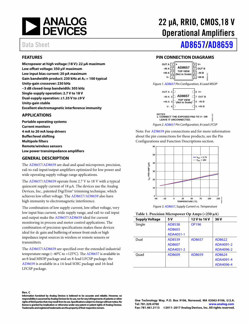
PIN CONNECTION DIAGRAMS OUT A 1
–IN A 2
+IN A 3
V– 4
V+8
OUT B7
–IN B6
+IN B5
AD8657TOP VIEW
(Not to Scale)
0880
4-00
1
Figure 1. AD8657 Pin Configuration, 8-Lead MSOP
0880
4-06
1
AD8657TOP VIEW
(Not to Scale)
NOTES1. CONNECT THE EXPOSED PAD TO V– OR LEAVE IT UNCONNECTED.
3+IN A
4V–
1OUT A
2–IN A
6 –IN B
5 +IN B
8 V+
7 OUT B
Figure 2. AD8657 Pin Configuration, 8-Lead LFCSP
Note: For AD8659 pin connections and for more information about the pin connections for these products, see the Pin Configurations and Function Descriptions section.
0
10
20
30
40
50
60
–50 –25 0 25 50 75 100 125
I SY
PER
AM
P (µ
A)
TEMPERATURE (°C)
VSY = 2.7VVSY = 18V
0880
4-02
3
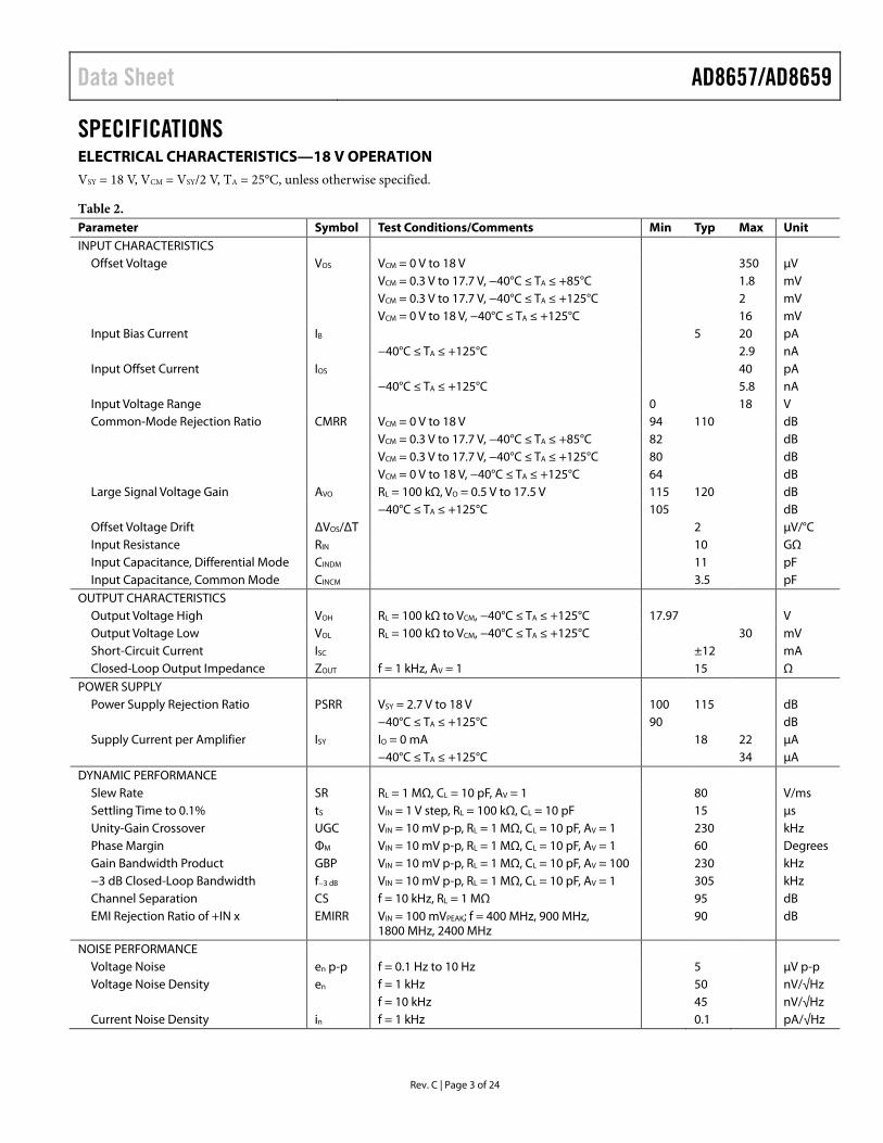
Figure 3. AD8657, Supply Current vs. Temperature
Table 1. Precision Micropower Op Amps (<250 μA) Supply Voltage 5 V 12 V to 16 V 36 V Single AD8538 OP196 AD8603 ADA4051-1 Dual AD8539 AD8657 AD8622 AD8607 ADA4091-2 ADA4051-2 ADA4096-2 Quad AD8609 AD8659 AD8624 ADA4091-4 ADA4096-4
AD8657/AD8659 Data Sheet
Rev. C | Page 2 of 24
TABLE OF CONTENTS Features .............................................................................................. 1
Applications ....................................................................................... 1
General Description ......................................................................... 1
Pin Connection Diagrams ............................................................... 1
Revision History ............................................................................... 2
Specifications ..................................................................................... 3
Electrical Characteristics—18 V Operation ............................. 3
Electrical Characteristics—10 V Operation ............................. 4
Electrical Characteristics—2.7 V Operation ............................ 5
Absolute Maximum Ratings ............................................................ 6
Thermal Resistance ...................................................................... 6
ESD Caution .................................................................................. 6
Pin Configurations and Function Descriptions ........................... 7
Typical Performance Characteristics ..............................................9
Applications Information .............................................................. 19
Input Stage ................................................................................... 19
Output Stage ................................................................................ 20
Rail to Rail ................................................................................... 20
Resistive Load ............................................................................. 20
Comparator Operation—AD8657 ........................................... 21
EMI Rejection Ratio .................................................................. 22
4 mA to 20 mA Process Control Current Loop Transmitter—AD8657 ........................................................................................ 22
Outline Dimensions ....................................................................... 23
Ordering Guide .......................................................................... 24
REVISION HISTORY 6/2017—Rev. B to Rev. A Change to 4 mA to 20 mA Process Control Current Loop Transmitter—AD8657 Section and Figure 78 ............................ 22 Updated Outline Dimensions ....................................................... 24 Changes to Ordering Guide .......................................................... 24 8/2012—Rev. A to Rev. B Added AD8659 ................................................................... Universal Changes to Features Section............................................................ 1 Changes to Pin Connection Diagrams Section ............................ 1 Added Figure 3, Renumbered Figures Sequentially ..................... 1 Changes to Table 1 ............................................................................ 1 Reordered Table 2 and Table 4 ........................................................ 3 Changes to Table 2 ............................................................................ 3 Changes to Table 3 ............................................................................ 4 Changes to Table 4 ............................................................................ 5 Changes to Table 6 ............................................................................ 6 Added Pin Configurations and Function Descriptions Section 7 Added Figure 4 and Figure 5 ........................................................... 7 Added Table 7, Renumbered Tables Sequentially ........................ 7 Added Figure 6 and Figure 7 ........................................................... 8 Added Table 8 .................................................................................... 8 Changes to Figure 10 and Figure 13 ............................................... 9 Changes to Figure 14, Figure 15, Figure 17, and Figure 18 ....... 10 Changes to Figure 28 and Figure 31 ............................................. 12 Changes to Figure 32 ...................................................................... 13 Changes to Figure 39 ...................................................................... 14 Changes to Figure 63 and Figure 66 ............................................. 18 Moved Figure 68 ............................................................................. 19
Change to Inverting Op Amp Configuration Section Heading and Changes to Figure 70 .............................................................. 20 Change to Noninverting Op Amp Configuration Heading and Changes to Figure 71 ...................................................................... 20 Change to Comparator Operation—AD8657 Heading ............ 21 Change to 4 mA to 20 mA Process Control Current Loop Transmitter—AD8657 Section Heading and Changed 33 μA to 34 μA ................................................................................ 22 Updated Outline Dimensions ....................................................... 24 Added Figure 81 and Figure 82 .................................................... 24 Changes to Ordering Guide .......................................................... 24 3/2011—Rev. 0 to Rev. A Added LFCSP Package Information ........................... Throughout Added Figure 2, Renumbered Subsequent Figures .................... 1 Changes to Table 2, Introductory Text; Input Characteristics, Offset Voltage and Common-Mode Rejection Ratio Test Conditions/Comments; and Dynamic Performance, Phase Margin Values .................................................................................... 3 Changes to Table 3, Introductory Text; Input Characteristics, Offset Voltage and Common-Mode Rejection Ratio Test Conditions/Comments ..................................................................... 4 Changes to Table 4, Introductory Text; Input Characteristics, Offset Voltage and Common-Mode Rejection Ratio Test Conditions/Comments ..................................................................... 5 Changes to Thermal Resistance Section and Table 5 ................... 6 Updated Outline Dimensions ....................................................... 21 Changes to Ordering Guide .......................................................... 21 1/2011—Revision 0: Initial Version
Data Sheet AD8657/AD8659
Rev. C | Page 3 of 24
SPECIFICATIONS ELECTRICAL CHARACTERISTICS—18 V OPERATION VSY = 18 V, VCM = VSY/2 V, TA = 25°C, unless otherwise specified.
Table 2. Parameter Symbol Test Conditions/Comments Min Typ Max Unit INPUT CHARACTERISTICS
Offset Voltage VOS VCM = 0 V to 18 V 350 µV VCM = 0.3 V to 17.7 V, −40°C ≤ TA ≤ +85°C 1.8 mV VCM = 0.3 V to 17.7 V, −40°C ≤ TA ≤ +125°C 2 mV VCM = 0 V to 18 V, −40°C ≤ TA ≤ +125°C 16 mV Input Bias Current IB 5 20 pA −40°C ≤ TA ≤ +125°C 2.9 nA Input Offset Current IOS 40 pA −40°C ≤ TA ≤ +125°C 5.8 nA Input Voltage Range 0 18 V Common-Mode Rejection Ratio CMRR VCM = 0 V to 18 V 94 110 dB VCM = 0.3 V to 17.7 V, −40°C ≤ TA ≤ +85°C 82 dB VCM = 0.3 V to 17.7 V, −40°C ≤ TA ≤ +125°C 80 dB VCM = 0 V to 18 V, −40°C ≤ TA ≤ +125°C 64 dB Large Signal Voltage Gain AVO RL = 100 kΩ, VO = 0.5 V to 17.5 V 115 120 dB −40°C ≤ TA ≤ +125°C 105 dB Offset Voltage Drift ΔVOS/ΔT 2 μV/°C Input Resistance RIN 10 GΩ Input Capacitance, Differential Mode CINDM 11 pF Input Capacitance, Common Mode CINCM 3.5 pF
OUTPUT CHARACTERISTICS Output Voltage High VOH RL = 100 kΩ to VCM, −40°C ≤ TA ≤ +125°C 17.97 V Output Voltage Low VOL RL = 100 kΩ to VCM, −40°C ≤ TA ≤ +125°C 30 mV Short-Circuit Current ISC ±12 mA Closed-Loop Output Impedance ZOUT f = 1 kHz, AV = 1 15 Ω
POWER SUPPLY Power Supply Rejection Ratio PSRR VSY = 2.7 V to 18 V 100 115 dB −40°C ≤ TA ≤ +125°C 90 dB Supply Current per Amplifier ISY IO = 0 mA 18 22 µA −40°C ≤ TA ≤ +125°C 34 µA
DYNAMIC PERFORMANCE Slew Rate SR RL = 1 MΩ, CL = 10 pF, AV = 1 80 V/ms Settling Time to 0.1% tS VIN = 1 V step, RL = 100 kΩ, CL = 10 pF 15 µs Unity-Gain Crossover UGC VIN = 10 mV p-p, RL = 1 MΩ, CL = 10 pF, AV = 1 230 kHz Phase Margin ΦM VIN = 10 mV p-p, RL = 1 MΩ, CL = 10 pF, AV = 1 60 Degrees Gain Bandwidth Product GBP VIN = 10 mV p-p, RL = 1 MΩ, CL = 10 pF, AV = 100 230 kHz −3 dB Closed-Loop Bandwidth f−3 dB VIN = 10 mV p-p, RL = 1 MΩ, CL = 10 pF, AV = 1 305 kHz Channel Separation CS f = 10 kHz, RL = 1 MΩ 95 dB EMI Rejection Ratio of +IN x EMIRR VIN = 100 mVPEAK; f = 400 MHz, 900 MHz,
1800 MHz, 2400 MHz 90 dB
NOISE PERFORMANCE Voltage Noise en p-p f = 0.1 Hz to 10 Hz 5 µV p-p Voltage Noise Density en f = 1 kHz 50 nV/√Hz f = 10 kHz 45 nV/√Hz Current Noise Density in f = 1 kHz 0.1 pA/√Hz
AD8657/AD8659 Data Sheet
Rev. C | Page 4 of 24
ELECTRICAL CHARACTERISTICS—10 V OPERATION VSY = 10 V, VCM = VSY/2 V, TA = 25°C, unless otherwise specified.
Table 3. Parameter Symbol Test Conditions/Comments Min Typ Max Unit INPUT CHARACTERISTICS
Offset Voltage VOS VCM = 0 V to 10 V 350 µV VCM = 0.3 V to 9.7 V, −40°C ≤ TA ≤ +85°C 1.6 mV VCM = 0.3 V to 9.7 V, −40°C ≤ TA ≤ +125°C 2 mV VCM = 0 V to 10 V, −40°C ≤ TA ≤ +125°C 16 mV Input Bias Current IB 2 15 pA −40°C ≤ TA ≤ +125°C 2.6 nA Input Offset Current IOS 30 pA −40°C ≤ TA ≤ +125°C 5.2 nA Input Voltage Range 0 10 V Common-Mode Rejection Ratio CMRR VCM = 0 V to 10 V 88 105 dB VCM = 0.3 V to 9.7 V, −40°C ≤ TA ≤ +85°C 76 dB VCM = 0.3 V to 9.7 V, −40°C ≤ TA ≤ +125°C 75 dB VCM = 0 V to 10 V, −40°C ≤ TA ≤ +125°C 59 dB Large Signal Voltage Gain AVO RL = 100 kΩ, VO = 0.5 V to 9.5 V 108 120 dB −40°C ≤ TA ≤ +125°C 100 dB Offset Voltage Drift ΔVOS/ΔT 2 μV/°C Input Resistance RIN 10 GΩ Input Capacitance, Differential Mode CINDM 11 pF Input Capacitance, Common Mode CINCM 3.5 pF
OUTPUT CHARACTERISTICS Output Voltage High VOH RL = 100 kΩ to VCM, −40°C ≤ TA ≤ +125°C 9.98 V Output Voltage Low VOL RL = 100 kΩ to VCM, −40°C ≤ TA ≤ +125°C 20 mV Short-Circuit Current ISC ±11 mA Closed-Loop Output Impedance ZOUT f = 1 kHz, AV = 1 15 Ω
POWER SUPPLY Power Supply Rejection Ratio PSRR VSY = 2.7 V to 18 V 100 115 dB −40°C ≤ TA ≤ +125°C 90 dB Supply Current per Amplifier ISY IO = 0 mA 18 22 µA −40°C ≤ TA ≤ +125°C 34 µA
DYNAMIC PERFORMANCE Slew Rate SR RL = 1 MΩ, CL = 10 pF, AV = 1 75 V/ms Settling Time to 0.1% ts VIN = 1 V step, RL = 100 kΩ, CL = 10 pF 15 µs Unity-Gain Crossover UGC VIN = 10 mV p-p, RL = 1 MΩ, CL = 10 pF, AV = 1 225 kHz Phase Margin ΦM VIN = 10 mV p-p, RL = 1 MΩ, CL = 10 pF, AV = 1 60 Degrees Gain Bandwidth Product GBP VIN = 10 mV p-p, RL = 1 MΩ, CL = 10 pF, AV = 100 230 kHz −3 dB Closed-Loop Bandwidth f−3 dB VIN = 10 mV p-p, RL = 1 MΩ, CL = 10 pF, AV = 1 300 kHz Channel Separation CS f = 10 kHz, RL = 1 MΩ 95 dB EMI Rejection Ratio of +IN x EMIRR VIN = 100 mVPEAK; f = 400 MHz, 900 MHz,
1800 MHz, 2400 MHz 90 dB
NOISE PERFORMANCE Voltage Noise en p-p f = 0.1 Hz to 10 Hz 5 µV p-p Voltage Noise Density en f = 1 kHz 50 nV/√Hz f = 10 kHz 45 nV/√Hz Current Noise Density in f = 1 kHz 0.1 pA/√Hz

Data Sheet AD8657/AD8659
Rev. C | Page 5 of 24
ELECTRICAL CHARACTERISTICS—2.7 V OPERATION VSY = 2.7 V, VCM = VSY/2 V, TA = 25°C, unless otherwise specified.
Table 4. Parameter Symbol Test Conditions/Comments Min Typ Max Unit INPUT CHARACTERISTICS
Offset Voltage VOS VCM = 0 V to 2.7 V 350 µV VCM = 0.3 V to 2.4 V, −40°C ≤ TA ≤ +85°C 1.2 mV VCM = 0.3 V to 2.4 V, −40°C ≤ TA ≤ +125°C 2.5 mV VCM = 0 V to 2.7 V, −40°C ≤ TA ≤ +125°C 16 mV Input Bias Current IB 1 10 pA −40°C ≤ TA ≤ +125°C 2.6 nA Input Offset Current IOS 20 pA −40°C ≤ TA ≤ +125°C 5.2 nA Input Voltage Range 0 2.7 V Common-Mode Rejection Ratio CMRR VCM = 0 V to 2.7 V 77 95 dB VCM = 0.3 V to 2.4 V, −40°C ≤ TA ≤ +85°C 69 dB VCM = 0.3 V to 2.4 V, −40°C ≤ TA ≤ +125°C 62 dB VCM = 0 V to 2.7 V, −40°C ≤ TA ≤ +125°C 47 dB Large Signal Voltage Gain AVO RL = 100 kΩ, VO = 0.5 V to 2.2 V 95 105 dB
−40°C ≤ TA ≤ +125°C 90 dB Offset Voltage Drift ΔVOS/ΔT 2 μV/°C Input Resistance RIN 10 GΩ Input Capacitance, Differential Mode CINDM 11 pF Input Capacitance, Common Mode CINCM 3.5 pF
OUTPUT CHARACTERISTICS Output Voltage High VOH RL = 100 kΩ to VCM, −40°C ≤ TA ≤ +125°C 2.69 V Output Voltage Low VOL RL = 100 kΩ to VCM, −40°C ≤ TA ≤ +125°C 10 mV Short-Circuit Current ISC ±4 mA Closed-Loop Output Impedance ZOUT f = 1 kHz, AV = 1 20 Ω
POWER SUPPLY Power Supply Rejection Ratio PSRR VSY = 2.7 V to 18 V 100 115 dB −40°C ≤ TA ≤ +125°C 90 dB Supply Current per Amplifier ISY IO = 0 mA 18 22 µA
−40°C ≤ TA ≤ +125°C 34 µA DYNAMIC PERFORMANCE
Slew Rate SR RL = 1 MΩ, CL = 10 pF, AV = 1 50 V/ms Settling Time to 0.1% ts VIN = 1 V step, RL = 100 kΩ, CL = 10 pF 20 µs Unity-Gain Crossover UGC VIN = 10 mV p-p, RL = 1 MΩ, CL = 10 pF, AV = 1 190 kHz Phase Margin ΦM VIN = 10 mV p-p, RL = 1 MΩ, CL = 10 pF, AV = 1 55 Degrees Gain Bandwidth Product GBP VIN = 10 mV p-p, RL = 1 MΩ, CL = 10 pF, AV = 100 200 kHz −3 dB Closed-Loop Bandwidth f−3 dB VIN = 10 mV p-p, RL = 1 MΩ, CL = 10 pF, AV = 1 245 kHz Channel Separation CS f = 10 kHz, RL = 1 MΩ 95 dB EMI Rejection Ratio of +IN x EMIRR VIN = 100 mVPEAK; f = 400 MHz, 900 MHz,
1800 MHz, 2400 MHz 90 dB
NOISE PERFORMANCE Voltage Noise en p-p f = 0.1 Hz to 10 Hz 6 µV p-p Voltage Noise Density en f = 1 kHz 60 nV/√Hz
f = 10 kHz 56 nV/√Hz Current Noise Density in f = 1 kHz 0.1 pA/√Hz

AD8657/AD8659 Data Sheet
Rev. C | Page 6 of 24
ABSOLUTE MAXIMUM RATINGS Table 5. Parameter Rating Supply Voltage 20.5 V Input Voltage (V−) − 300 mV to (V+) + 300 mV Input Current1 ±10 mA Differential Input Voltage ±VSY Output Short-Circuit
Duration to GND Indefinite
Temperature Ranges Storage −65°C to +150°C Operating −40°C to +125°C Junction −65°C to +150°C
Lead Temperature (Soldering, 60 sec)
300°C
1 The input pins have clamp diodes to the power supply pins. Limit the input
current to 10 mA or less whenever input signals exceed the power supply rail by 0.3 V.
Stresses at or above those listed under Absolute Maximum Ratings may cause permanent damage to the product. This is a stress rating only; functional operation of the product at these or any other conditions above those indicated in the operational section of this specification is not implied. Operation beyond the maximum operating conditions for extended periods may affect product reliability.
THERMAL RESISTANCE θJA is specified for the worst-case conditions, that is, a device soldered in a circuit board for surface-mount packages using a standard 4-layer JEDEC board. The exposed pad (LFCSP packages only) is soldered to the board.
Table 6. Thermal Resistance Package Type θJA θJC Unit 8-Lead MSOP (RM-8) 142 45 °C/W 8-Lead LFCSP (CP-8-11) 75 12 °C/W 14-Lead SOIC (R-14) 115 36 °C/W 16-Lead LFCSP (CP-16-20) 52 13 °C/W
ESD CAUTION
Data Sheet AD8657/AD8659
Rev. C | Page 7 of 24
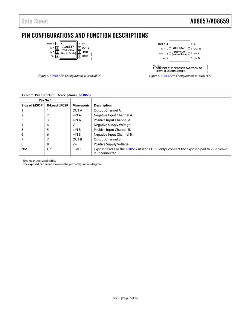
PIN CONFIGURATIONS AND FUNCTION DESCRIPTIONS OUT A 1
–IN A 2
+IN A 3
V– 4
V+8
OUT B7
–IN B6
+IN B5
AD8657TOP VIEW
(Not to Scale)
0880
4-00
1
Figure 4. AD8657 Pin Configuration, 8-Lead MSOP
0880
4-06
1
AD8657TOP VIEW
(Not to Scale)
NOTES1. CONNECT THE EXPOSED PAD TO V– OR LEAVE IT UNCONNECTED.
3+IN A
4V–
1OUT A
2–IN A
6 –IN B
5 +IN B
8 V+
7 OUT B
Figure 5. AD8657 Pin Configuration, 8-Lead LFCSP
Table 7. Pin Function Descriptions, AD8657 Pin No.1
Mnemonic Description 8-Lead MSOP 8-Lead LFCSP 1 1 OUT A Output Channel A. 2 2 −IN A Negative Input Channel A. 3 3 +IN A Positive Input Channel A. 4 4 V− Negative Supply Voltage. 5 5 +IN B Positive Input Channel B. 6 6 −IN B Negative Input Channel B. 7 7 OUT B Output Channel B. 8 8 V+ Positive Supply Voltage. N/A EP2 EPAD Exposed Pad. For the AD8657 (8-lead LFCSP only), connect the exposed pad to V− or leave
it unconnected. 1 N/A means not applicable. 2 The exposed pad is not shown in the pin configuration diagram.

AD8657/AD8659 Data Sheet
Rev. C | Page 8 of 24
OUT A 1
–IN A 2
+IN A 3
V+ 4
OUT D14
–IN D13
+IN D12
V–11
+IN B 5 +IN C10
–IN B 6 –IN C9
OUT B 7 OUT C8
AD8659TOP VIEW
(Not to Scale)
0880
4-10
3
Figure 6. AD8659 Pin Configuration, 14-Lead SOIC_N
NOTES1. NIC = NO INTERNAL CONNECTION.2. CONNECT THE EXPOSED PAD TO V– OR LEAVE IT UNCONNECTED.
–IN D
+IN D
V–
+IN C
–IN A
V+
+IN A
+IN B
OU
T B
–IN
B
OU
T C
–IN
C
NIC
OU
T A
OU
T D
NC
0880
4-10
4
12
11
10
1
3
4 9
2
65 7 8
16 15 14 13
TOP VIEW(Not to Scale)
AD8659
Figure 7. AD8659 Pin Configuration, 16-Lead LFCSP
Table 8. Pin Function Descriptions, AD8659 Pin No.1
Mnemonic Description 14-Lead SOIC 16-Lead LFCSP 1 15 OUT A Output Channel A. 2 1 −IN A Negative Input Channel A. 3 2 +IN A Positive Input Channel A. 11 10 V− Negative Supply Voltage. 5 4 +IN B Positive Input Channel B. 6 5 −IN B Negative Input Channel B. 7 6 OUT B Output Channel B. 4 3 V+ Positive Supply Voltage. 8 7 OUT C Output Channel C. 9 8 −IN C Negative Input Channel C. 10 9 +IN C Positive Input Channel C. 12 11 +IN D Positive Input Channel D. 13 12 −IN D Negative Input Channel D. 14 14 OUT D Output Channel D. N/A 13 NIC No Internal Connection. N/A 16 NIC No Internal Connection. N/A EP2 EPAD2 Exposed Pad. For the AD8659 (16-lead LFCSP only), connect the exposed pad to
V− or leave it unconnected. 1 N/A means not applicable. 2 The exposed pad is not shown in the pin configuration diagram.

Data Sheet AD8657/AD8659
Rev. C | Page 9 of 24
TYPICAL PERFORMANCE CHARACTERISTICS TA = 25°C, unless otherwise noted.
20
40
60
80
100
120
140
160
NU
MB
ER O
FA
MPL
IFIE
RS
VSY = 2.7VVCM = VSY/2
0
–140
–120
–100 –8
0
–60
–40
–20 0 20 40 60 80 100
120
140
VOS (µV)
0880
4-00
2
Figure 8. Input Offset Voltage Distribution
0
2
4
6
8
10
12
14
16
18
0 0.5 1.0 1.5 2.0 2.5 3.0 3.5 4.0 4.5 5.0 5.5 6.0 6.5 7.0
NU
MB
ER O
FA
MPL
IFIE
RS
TCVOS (µV/°C)
VSY = 2.7V–40°C ≤ TA ≤ +125°C
0880
4-00
3
Figure 9. Input Offset Voltage Drift Distribution
–350
–250
–150
–50
50
150
250
350
0 0.3 0.6 0.9 1.2 1.5 1.8 2.1 2.4 2.7
V OS
(µV)
VCM (V)
VSY = 2.7V
0880
4-20
7
Figure 10. Input Offset Voltage vs. Common-Mode Voltage
0
20
40
60
80
100
120
140
160
–140
–120
–100 –8
0
–60
–40
–20 0 20 40 60 80 100
120
140
NU
MB
ER O
FA
MPL
IFIE
RS
VOS (µV)
VSY = 18VVCM = VSY/2
0880
4-00
5
Figure 11. Input Offset Voltage Distribution
0
2
4
6
8
10
12
14
18
16
20
0 0.5 1.0 1.5 2.0 2.5 3.0 3.5 4.0 4.5 5.0 5.5 6.0 6.5 7.0
NU
MB
ER O
FA
MPL
IFIE
RS
TCVOS (µV/°C)
VSY = 18V–40°C ≤ TA ≤ +125°C
0880
4-00
6
Figure 12. Input Offset Voltage Drift Distribution
–350
–250
–150
–50
50
150
250
350
0 2 4 6 8 10 12 14 16 18
V OS
(µV)
VCM (V)
0880
4-21
0
VSY = 18V
Figure 13. Input Offset Voltage vs. Common-Mode Voltage

AD8657/AD8659 Data Sheet
Rev. C | Page 10 of 24
–3.0
–2.5
–2.0
–1.5
–1.0
–0.5
0
0.5
1.0
1.5
2.0
2.5
3.0
0 0.3 0.6 0.9 1.2 1.5 1.8 2.1 2.4 2.7
V OS
(mV)
VCM (V)
VSY = 2.7V–40°C ≤ TA ≤ +85°C
0880
4-21
1
Figure 14. Input Offset Voltage vs. Common-Mode Voltage
–6
–4
–2
0
2
4
6
0 0.3 0.6 0.9 1.2 1.5 1.8 2.1 2.4 2.7
V OS
(mV)
VCM (V)
VSY = 2.7V–40°C ≤ TA ≤ +125°C
0880
4-21
2
Figure 15. Input Offset Voltage vs. Common-Mode Voltage
0.1
1
10
100
1000
10000
25 50 75 100 125
I B (p
A)
TEMPERATURE (°C)
IB+IB–
VSY = 2.7V
0880
4-00
8
Figure 16. Input Bias Current vs. Temperature
–3.0
–2.5
–2.0
–1.5
–1.0
–0.5
0
0.5
1.0
1.5
2.0
2.5
3.0
0 2 4 6 8 10 12 14 16 18
V OS
(mV)
VCM (V)
VSY = 18V–40°C < TA < +85°C
0880
4-21
4
Figure 17. Input Offset Voltage vs. Common-Mode Voltage
–6
–4
–2
0
2
4
6
0 2 4 6 8 10 12 14 16 18
V OS
(mV)
VCM (V)
VSY = 18V–40°C ≤ TA ≤ +125°C
0880
4-21
5
Figure 18. Input Offset Voltage vs. Common-Mode Voltage
0.1
1
10
100
1000
10000
25 50 75 100 125
I B (p
A)
TEMPERATURE (°C)
VSY = 18V
0880
4-01
1IB+IB–
Figure 19. Input Bias Current vs. Temperature
Data Sheet AD8657/AD8659
Rev. C | Page 11 of 24
–4
–3
–2
–1
0
1
2
3
4
0 0.3 0.6 0.9 1.2 1.5 1.8 2.1 2.4 2.7
I B (n
A)
VCM (V)
25°C85°C125°C
VSY = 2.7V
0880
4-00
9
Figure 20. Input Bias Current vs. Common-Mode Voltage
0.01m
0.1m
1m
10m
100m
1
10
0.001 0.01 0.1 1 10 100
OU
TPU
T VO
LTA
GE
(VO
H)T
O S
UPP
LY R
AIL
(V)
LOAD CURRENT (mA)
–40°C+25°C+85°C+125°C
VSY = 2.7V
0880
4-01
0
Figure 21. Output Voltage (VOH) to Supply Rail vs. Load Current
0.01m
0.1m
1m
10m
100m
1
10
0.001 0.01 0.1 1 10 100
OU
TPU
T VO
LTA
GE
(VO
L)TO
SU
PPLY
RA
I L (V
)
LOAD CURRENT (mA)
–40°C+25°C+85°C+125°C
VSY = 2.7V
0880
4-01
4
Figure 22. Output Voltage (VOL) to Supply Rail vs. Load Current
0 2 4 6 8 10 12 14 16 18VCM (V)
25°C85°C125°C
VSY = 18V
0880
4-01
2
–4
–3
–2
–1
0
1
2
3
4
I B (n
A)
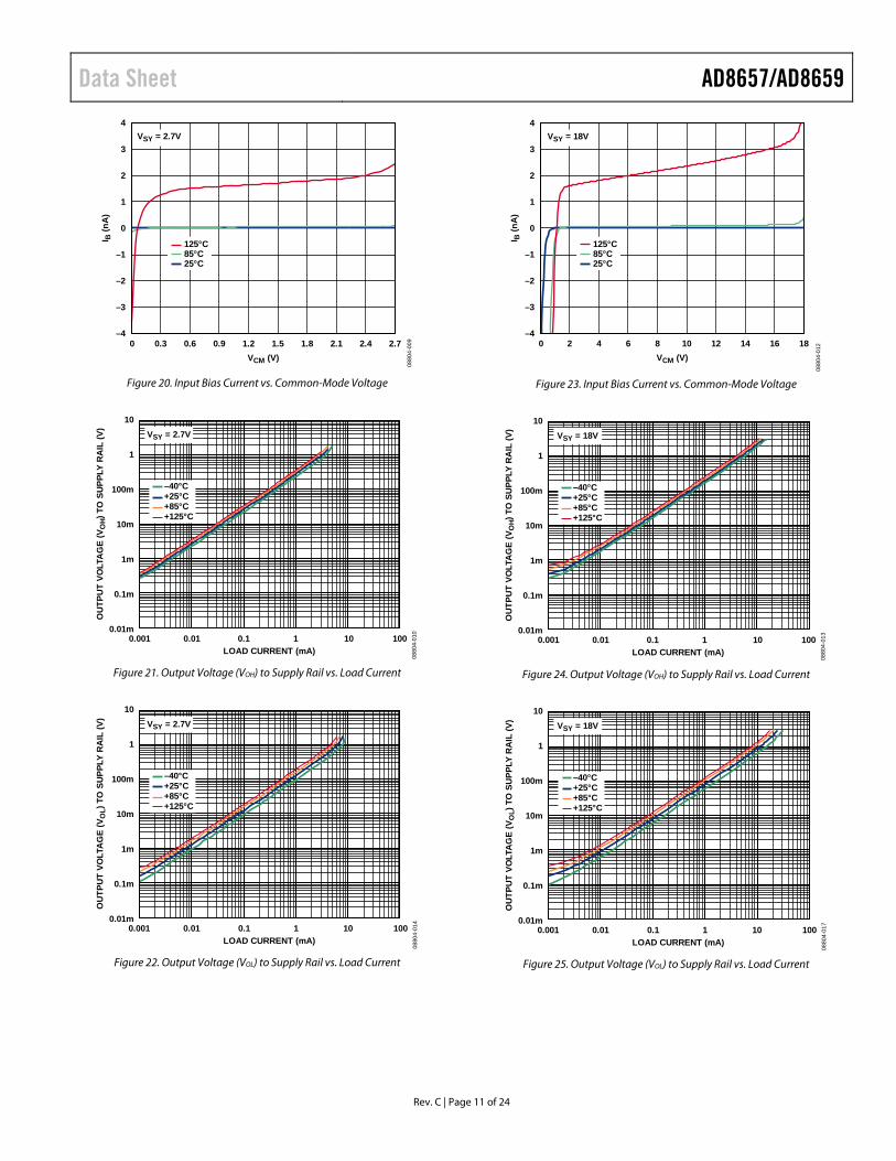
Figure 23. Input Bias Current vs. Common-Mode Voltage
0.01m
0.1m
1m
10m
100m
1
10
OU
TPU
T VO
LTA
GE
(VO
H)T
O S
UPP
LY R
AIL
(V)
LOAD CURRENT (mA)
–40°C+25°C+85°C+125°C
VSY = 18V
0.001 0.01 0.1 1 10 100
0880
4-01
3
Figure 24. Output Voltage (VOH) to Supply Rail vs. Load Current
0.01m
0.1m
1m
10m
100m
1
10
0.001 0.01 0.1 1 10 100
OU
TPU
T VO
LTA
GE
(VO
L)TO
SU
PPLY
RA
I L (V
)
LOAD CURRENT (mA)
–40°C+25°C+85°C+125°C
VSY = 18V
0880
4-01
7
Figure 25. Output Voltage (VOL) to Supply Rail vs. Load Current

AD8657/AD8659 Data Sheet
Rev. C | Page 12 of 24
2.695
2.696
2.697
2.698
2.699
2.700
–50 –25 0 25 50 75 100 125
OU
TPU
T VO
LTA
GE,
VO
H (V
)
TEMPERATURE (°C)
RL = 100kΩ
RL = 1MΩ
VSY = 2.7V
0880
4-01
5
Figure 26. Output Voltage (VOH) vs. Temperature
0
2
4
6
8
10
12
–50 –25 0 25 50 75 100 125
OU
TPU
T VO
LTA
GE,
VO
L (m
V)
TEMPERATURE (°C)
RL = 100kΩ
RL = 1MΩ
VSY = 2.7V
0880
4-01
6
Figure 27. Output Voltage (VOL) vs. Temperature
0
5
10
15
20
25
30
35
0 0.3 0.6 0.9 1.2 1.5 1.8 2.1 2.4 2.7
I SY
PER
AM
P (µ
A)
VCM (V)
–40°C+25°C+85°C+125°C
VSY = 2.7V
0880
4-22
5
Figure 28. Supply Current vs. Common-Mode Voltage
17.975
17.980
17.985
17.990
17.995
18.000
–50 –25 0 25 50 75 100 125
OU
TPU
T VO
LTA
GE,
VO
H (V
)
TEMPERATURE (°C)
RL = 100kΩ
RL = 1MΩ
VSY = 18V
0880
4-01
8
Figure 29. Output Voltage (VOH) vs. Temperature
0
2
4
6
8
10
12
–50 –25 0 25 50 75 100 125
OU
TPU
T VO
LTA
GE,
VO
L (m
V)
TEMPERATURE (°C)
RL = 100kΩ
RL = 1MΩ
VSY = 18V
0880
4-01
9
Figure 30. Output Voltage (VOL) vs. Temperature
0
5
10
15
20
25
30
35
0 3 6 9 12 15 18
I SY
PER
AM
P (µ
A)
VCM (V)
VSY = 18V
–40°C+25°C+85°C+125°C
0880
4-22
8
Figure 31. Supply Current vs. Common-Mode Voltage
Data Sheet AD8657/AD8659
Rev. C | Page 13 of 24
0
5
10
15
20
25
30
35
40
0 3 6 9 12 15 18
–40°C+25°C+85°C+125°C
I SY
PER
AM
P (µ
A)
VSY (V)
0880
4-22
9
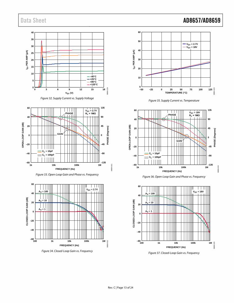
Figure 32. Supply Current vs. Supply Voltage
–135
–90
–45
0
45
90
135
–60
–20
–40
0
20
40
60
1k 10k 100k 1M
PHA
SE (D
egre
es)
OPE
N-L
OO
P G
AIN
(dB
)
FREQUENCY (Hz)
VSY = 2.7VRL = 1MΩPHASE
GAIN
0880
4-02
1
CL = 10pFCL = 100pF
Figure 33. Open-Loop Gain and Phase vs. Frequency
–60
–40
–20
0
20
40
60
100 1k 10k 100k 1M
CLO
SED
-LO
OP
GA
IN (d
B)
FREQUENCY (Hz)
VSY = 2.7VAV = 100
AV = 10
AV = 1
0880
4-02
2
Figure 34. Closed-Loop Gain vs. Frequency
0
10
20
30
40
50
60
–50 –25 0 25 50 75 100 125
I SY
PER
AM
P (µ
A)
TEMPERATURE (°C)
VSY = 2.7VVSY = 18V
0880
4-02
3
Figure 35. Supply Current vs. Temperature
1k 10k 100k 1M
OPE
N-L
OO
P G
AIN
(dB
)
FREQUENCY (Hz)
VSY = 18VRL = 1MΩ
0880
4-02
4
PHASE
CL = 10pFCL = 100pF
–135
–90
–45
0
45
90
135
–60
–20
–40
0
20
40
60
GAIN
PHA
SE (D
egre
es)
Figure 36. Open-Loop Gain and Phase vs. Frequency
–60
–40
–20
0
20
40
60
100 1k 10k 100k 1M
CLO
SED
-LO
OP
GA
IN (d
B)
FREQUENCY (Hz)
VSY = 18VAV = 100
AV = 10
AV = 108
804-
025
Figure 37. Closed-Loop Gain vs. Frequency
AD8657/AD8659 Data Sheet
Rev. C | Page 14 of 24
1
10
100
1000
100 1k 10k 100k
Z OU
T (Ω
)
FREQUENCY (Hz)
VSY = 2.7V
AV = 1
AV = 10AV = 100
0880
4-02
6
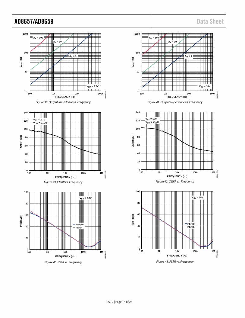
Figure 38. Output Impedance vs. Frequency
0
20
40
60
80
100
120
140
100 1k 10k 100k 1M
CM
RR
(dB
)
FREQUENCY (Hz) 0880
4-23
6
VSY = 2.7VVCM = VSY/2
Figure 39. CMRR vs. Frequency
0
20
40
60
80
100
100 1k 10k 100k 1M
PSR
R (d
B)
FREQUENCY (Hz)
PSRR+PSRR–
VSY = 2.7V
0880
4-02
8
Figure 40. PSRR vs. Frequency
1
10
100
1000
100 1k 10k 100k
Z OU
T (Ω
)
FREQUENCY (Hz)
VSY = 18V
AV = 1
AV = 10AV = 100
0880
4-02
9
Figure 41. Output Impedance vs. Frequency
100 1k 10k 100k 1M
CM
RR
(dB
)
FREQUENCY (Hz)
VSY = 18VVCM = VSY/2
0
20
40
60
80
100
120
140
0880
4-03
0
Figure 42. CMRR vs. Frequency
0
20
40
60
80
100
100 1k 10k 100k 1M
PSR
R (d
B)
FREQUENCY (Hz)
PSRR+PSRR–
VSY = 18V
0880
4-03
1
Figure 43. PSRR vs. Frequency
Data Sheet AD8657/AD8659
Rev. C | Page 15 of 24
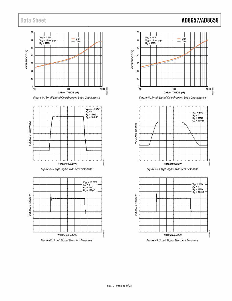
0
10
20
30
40
50
60
70
10 100 1000
OV
ER
SH
OO
T (
%)
CAPACITANCE (pF)
VSY = 2.7VVIN = 10mV p-pRL = 1MΩ
OS+OS–
0880
4-03
2
Figure 44. Small Signal Overshoot vs. Load Capacitance
TIME (100µs/DIV)
VO
LT
AG
E (
500m
V/D
IV)
VSY = ±1.35VAV = 1RL = 1MΩCL = 100pF
0880
4-03
3
Figure 45. Large Signal Transient Response
TIME (100µs/DIV)
VO
LT
AG
E (
5mV
/DIV
)
VSY = ±1.35VAV = 1RL = 1MΩCL = 100pF
0880
4-03
4
Figure 46. Small Signal Transient Response
0
10
20
30
40
50
60
70
10 100 1000
OV
ER
SH
OO
T (
%)
CAPACITANCE (pF)
VSY = 18VVIN = 10mV p-pRL = 1MΩ
OS+OS–
0880
4-03
5
Figure 47. Small Signal Overshoot vs. Load Capacitance
TIME (100µs/DIV)
VO
LT
AG
E (
5V/D
IV)
VSY = ±9VAV = 1RL = 1MΩCL = 100pF
0880
4-03
6
Figure 48. Large Signal Transient Response
TIME (100µs/DIV)
VO
LT
AG
E (
5mV
/DIV
)
VSY = ±9VAV = 1RL = 1MΩCL = 100pF
0880
4-03
7
Figure 49. Small Signal Transient Response

AD8657/AD8659 Data Sheet
Rev. C | Page 16 of 24
TIME (40µs/DIV)
–0.4
–0.2
0
2
1
0
INP
UT
VO
LT
AG
E (
V)
OU
TP
UT
VO
LT
AG
E (
V)
VSY = ±1.35AV = –10RL = 1MΩ
INPUT
OUTPUT
0880
4-03
9
Figure 50. Positive Overload Recovery
TIME (40µs/DIV)
0
0.2
0.4
0
–1
–2
INP
UT
VO
LT
AG
E (
V)
OU
TP
UT
VO
LT
AG
E (
V)
VSY = ±1.35VAV = –10RL = 1MΩ
INPUT
OUTPUT
0880
4-03
8
Figure 51. Negative Overload Recovery
TIME (10µs/DIV)
0
+5mV
–5mV
VO
LT
AG
E (
500m
V/D
IV)
VSY = 2.7VRL = 100kΩCL = 10pF
INPUT
OUTPUTERROR BAND
0880
4-04
0
Figure 52. Positive Settling Time to 0.1%
TIME (40µs/DIV)
–1
0
–2
10
5
0
INP
UT
VO
LT
AG
E (
V)
OU
TP
UT
VO
LT
AG
E (
V)
VSY = ±9VAV = –10RL = 1MΩ
INPUT
OUTPUT
0880
4-04
2
Figure 53. Positive Overload Recovery
TIME (40µs/DIV)
0
1
2
0
–5
–10
INP
UT
VO
LT
AG
E (
V)
OU
TP
UT
VO
LT
AG
E (
V)
VSY = ±9VAV = –10RL = 1MΩ
INPUT
OUTPUT
0880
4-04
1
Figure 54. Negative Overload Recovery
TIME (10µs/DIV)
0
+5mV
–5mV
VO
LT
AG
E (
500m
V/D
IV)
VSY = 18VRL = 100kΩCL = 10pF
INPUT
OUTPUTERROR BAND
0880
4-04
3
Figure 55. Positive Settling Time to 0.1%

Data Sheet AD8657/AD8659
Rev. C | Page 17 of 24
TIME (10µs/DIV)
0
+5mV
–5mV
VO
LT
AG
E (
500m
V/D
IV)
VSY = 2.7VRL = 100kΩCL = 10pF
INPUT
OUTPUT
ERROR BAND
0880
4-04
4
Figure 56. Negative Settling Time to 0.1%
1
10
100
1000
10 100 1k 10k 100k 1M
VO
LTA
GE
NO
ISE
DE
NS
ITY
(n
V/√
Hz)
FREQUENCY (Hz)
VSY = 2.7V08
804-
045
Figure 57. Voltage Noise Density vs. Frequency
TIME (2s/DIV)
VO
LT
AG
E (
2µV
/DIV
)
VSY = 2.7V
0880
4-04
6
Figure 58. 0.1 Hz to 10 Hz Noise
TIME (10µs/DIV)
0
+5mV
–5mV
VO
LT
AG
E (
500m
V/D
IV)
VSY =18VRL = 100kΩCL = 10pF
INPUT
OUTPUT
ERROR BAND
0880
4-04
7
Figure 59. Negative Settling Time to 0.1%
1
10
100
1000
10 100 1k 10k 100k 1M
VO
LTA
GE
NO
ISE
DE
NS
ITY
(n
V/√
Hz)
FREQUENCY (Hz)
VSY = 18V
0880
4-04
8
Figure 60. Voltage Noise Density vs. Frequency
TIME (2s/DIV)
VO
LT
AG
E (
2µV
/DIV
)
VSY = 18V
0880
4-04
9
Figure 61. 0.1 Hz to 10 Hz Noise

AD8657/AD8659 Data Sheet
Rev. C | Page 18 of 24
0
0.5
1.0
1.5
2.0
2.5
3.0
10 100 1k 10k 100k 1M
OU
TPU
T SW
ING
(V)
FREQUENCY (Hz)
VSY = 2.7VVIN = 2.6VRL = 1MΩAV = 1
0880
4-05
0
Figure 62. Output Swing vs. Frequency
0.01
0.1
1
10
10 100 1k 10k 100k
THD
+ N
(%)
FREQUENCY (Hz)
VSY = 2.7VVIN = 0.2V RMSRL = 1MΩAV = 1
0880
4-26
0
Figure 63. THD + N vs. Frequency
–140
–120
–100
–80
–60
–40
–20
0
100 1k 10k 100k
CH
AN
NE
L SE
PAR
ATIO
N (d
B)
FREQUENCY (Hz)
VIN = 0.5V p-pVIN = 1.5V p-pVIN = 2.6V p-p
VSY = 2.7VRL = 1MΩAV = –100
0880
4-05
2
RL
1MΩ10kΩ
Figure 64. Channel Separation vs. Frequency
10 100 1k 10k 100k 1M
OU
TPU
T SW
ING
(V)
FREQUENCY (Hz)
0
2
4
6
8
10
12
14
16
18
20
VSY = 18VVIN = 17.9VRL = 1MΩAV = 1
0880
4-05
3
Figure 65. Output Swing vs. Frequency
0.001
0.01
0.1
1
10
100
10 100 1k 10k 100k
THD
+ N
(%)
FREQUENCY (Hz) 0880
4-26
3
VSY = 18VVIN = 0.2V RMSRL = 1MΩAV = 1
Figure 66. THD + N vs. Frequency
–140
–120
–100
–80
–60
–40
–20
0
100 1k 10k 100k
CH
AN
NE
L SE
PAR
ATIO
N (d
B)
FREQUENCY (Hz)
VSY = 18VRL = 1MΩAV = –100
VIN = 1V p-pVIN = 5V p-pVIN = 10V p-pVIN = 15V p-pVIN = 17V p-p
0880
4-05
5
RL
1MΩ10kΩ
Figure 67. Channel Separation vs. Frequency

Data Sheet AD8657/AD8659
Rev. C | Page 19 of 24
APPLICATIONS INFORMATION V+
V–
+IN x R1
D1 D2
M1 M2
M7 M6
M3 M4M5
VB1 M8
M10
M9
M16
M17
M11
VB2 OUT x
M12
M14
M13
M15
I1
R2–IN x
0880
4-05
6
Figure 68. Simplified Schematic
The AD8657/AD8659 are low power, rail-to-rail input and output precision CMOS amplifiers that operate over a wide supply voltage range of 2.7 V to 18 V. The AD8657/AD8659 use the Analog Devices DigiTrim technique to achieve a higher degree of precision than is available from other CMOS amplifiers. The DigiTrim technique is a method of trimming the offset voltage of an amplifier after assembly. The advantage of post-package trimming is that it corrects any shifts in offset voltage caused by mechanical stresses of assembly.
The AD8657/AD8659 also employ unique input and output stages to achieve a rail-to-rail input and output range with a very low supply current.
INPUT STAGE Figure 68 shows the simplified schematic of the AD8657/AD8659. The input stage comprises two differential transistor pairs, an NMOS pair (M1, M2) and a PMOS pair (M3, M4). The input common-mode voltage determines which differential pair turns on and is more active than the other.
The PMOS differential pair is active when the input voltage approaches and reaches the lower supply rail. The NMOS pair is needed for input voltages up to and including the upper supply rail. This topology allows the amplifier to maintain a wide dynamic input voltage range and to maximize signal swing to both supply rails.
For the majority of the input common-mode voltage range, the PMOS differential pair is active. Differential pairs commonly exhibit different offset voltages. The handoff from one pair to the other creates a step-like characteristic that is visible in the VOS vs. VCM graphs (see Figure 10 and Figure 13). This characteristic is inherent in all rail-to-rail amplifiers that use the dual differential pair topology. Therefore, always choose a common-mode voltage that does not include the region of handoff from one input differential pair to the other.
Additional steps in the VOS vs. VCM curves are also visible as the input common-mode voltage approaches the power supply rails.
These changes are a result of the load transistors (M8, M9, M14, and M15) running out of headroom. As the load transistors are forced into the triode region of operation, the mismatch of their drain impedances contributes to the offset voltage of the amplifier. This problem is exacerbated at high temperatures due to the decrease in the threshold voltage of the input transistors (see Figure 14, Figure 15, Figure 17, and Figure 18 for typical perfor-mance data).
Current Source I1 drives the PMOS transistor pair. As the input common-mode voltage approaches the upper rail, I1 is steered away from the PMOS differential pair through the M5 transistor. The bias voltage, VB1 (see Figure 68), controls the point where this transfer occurs. M5 diverts the tail current into a current mirror consisting of the M6 and M7 transistors. The output of the current mirror then drives the NMOS pair. Note that the activation of this current mirror causes a slight increase in supply current at high common-mode voltages (see Figure 28 and Figure 31 for more details).
The AD8657/AD8659 achieve their high performance by using low voltage MOS devices for their differential inputs. These low voltage MOS devices offer excellent noise and bandwidth per unit of current. Each differential input pair is protected by proprie-tary regulation circuitry (not shown in the simplified schematic). The regulation circuitry consists of a combination of active devices that maintain the proper voltages across the input pairs during normal operation and passive clamping devices that protect the amplifier during fast transients. However, these passive clamping devices begin to forward bias as the common-mode voltage approaches either power supply rail, thereby causing an increase in the input bias current (see Figure 20 and Figure 23).
The input devices are also protected from large differential input voltages by clamp diodes (D1 and D2). These diodes are buffered from the inputs with two 10 kΩ resistors (R1 and R2). The differential diodes turn on whenever the differential voltage exceeds approximately 600 mV; in this condition, the differential input resistance drops to 20 kΩ.

AD8657/AD8659 Data Sheet
Rev. C | Page 20 of 24
OUTPUT STAGE The AD8657/AD8659 feature a complementary output stage consisting of the M16 and M17 transistors. These transistors are configured in Class AB topology and are biased by the voltage source, VB2. This topology allows the output voltage to go within millivolts of the supply rails, achieving a rail-to-rail output swing. The output voltage is limited by the output impedance of the transistors, which are low RON MOS devices. The output voltage swing is a function of the load current and can be estimated using the output voltage to the supply rail vs. load current diagrams (see Figure 21, Figure 22, Figure 24, and Figure 25).
RAIL TO RAIL The AD8657/AD8659 feature rail-to-rail input and output with a supply voltage from 2.7 V to 18 V. Figure 69 shows the input and output waveforms of the AD8657/AD8659 configured as a unity-gain buffer with a supply voltage of ±9 V and a resistive load of 1 MΩ. With an input voltage of ±9 V, the AD8657/AD8659 allow the output to swing very close to both rails. Additionally, they do not exhibit phase reversal.
TIME (200µs/DIV)
VO
LT
AG
E (
5V/D
IV)
VSY = ±9VRL = 1MΩ
0880
4-05
7
INPUTOUTPUT
Figure 69. Rail-to-Rail Input and Output
RESISTIVE LOAD The feedback resistor alters the load resistance that an amplifier sees. It is, therefore, important to be aware of the value of feed-back resistors chosen for use with the AD8657/AD8659. The amplifiers are capable of driving resistive loads down to 100 kΩ. The following two examples, inverting and noninverting configurations, show how the feedback resistor changes the actual load resistance seen at the output of the amplifier.
Inverting Op Amp Configuration
Figure 70 shows the AD8657/AD8659 in an inverting configu-ration with a resistive load, RL, at the output. The actual load seen by the amplifier is the parallel combination of the feedback resistor, R2, and load, RL. For example, the combination of a feed-back resistor of 1 kΩ and a load of 1 MΩ results in an equivalent load resistance of 999 Ω at the output. Because the AD8657/ AD8659 are incapable of driving such a heavy load, performance degrades greatly.
To avoid loading the output, use a larger feedback resistor, but consider the resistor thermal noise effect on the overall circuit.
AD8657/AD8659
R1
R2
RL
–VSY
RL, EFF = RL || R2
+VSY
VIN
VOUT
0880
4-05
8
Figure 70. Inverting Op Amp Configuration
Noninverting Op Amp Configuration
Figure 71 shows the AD8657/AD8659 in a noninverting configu-ration with a resistive load, RL, at the output. The actual load seen by the amplifier is the parallel combination of R1 + R2 and RL.
R1
R2
RL
–VSY
RL, EFF = RL || (R1 + R2)
+VSY
VIN
VOUT
0880
4-05
9
AD8657/AD8659
Figure 71. Noninverting Op Amp Configuration
Data Sheet AD8657/AD8659
Rev. C | Page 21 of 24
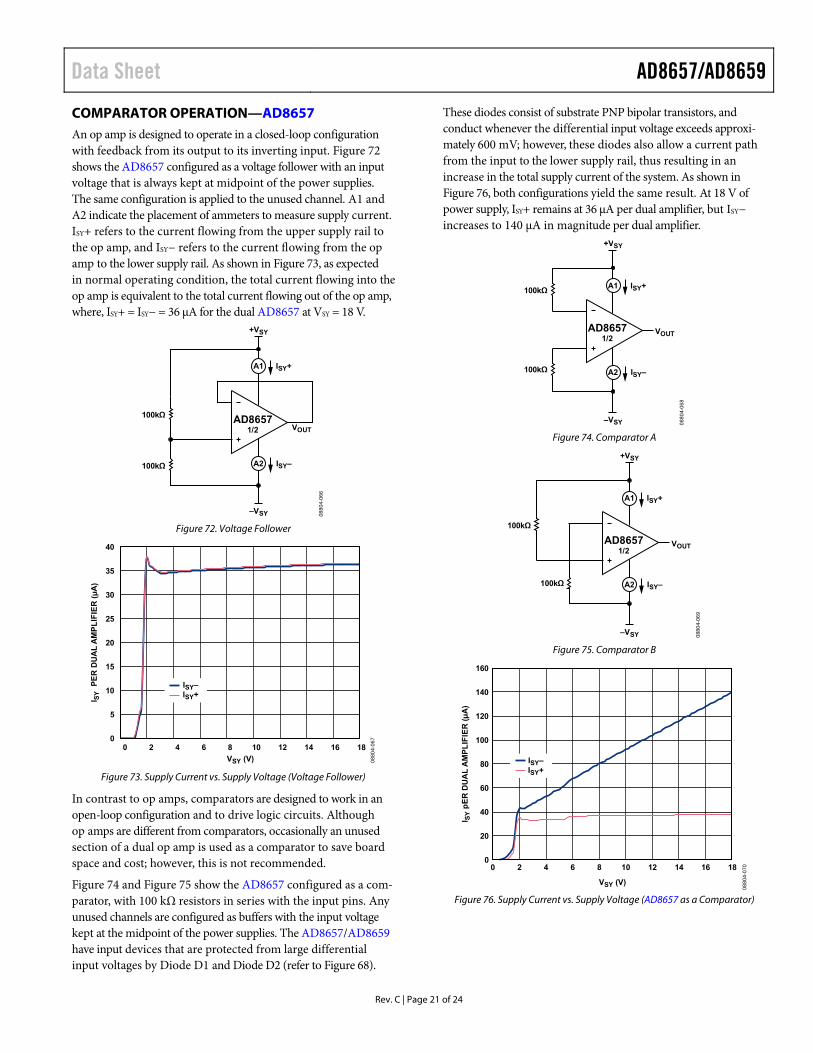
COMPARATOR OPERATION—AD8657 An op amp is designed to operate in a closed-loop configuration with feedback from its output to its inverting input. Figure 72 shows the AD8657 configured as a voltage follower with an input voltage that is always kept at midpoint of the power supplies. The same configuration is applied to the unused channel. A1 and A2 indicate the placement of ammeters to measure supply current. ISY+ refers to the current flowing from the upper supply rail to the op amp, and ISY− refers to the current flowing from the op amp to the lower supply rail. As shown in Figure 73, as expected in normal operating condition, the total current flowing into the op amp is equivalent to the total current flowing out of the op amp, where, ISY+ = ISY− = 36 μA for the dual AD8657 at VSY = 18 V.
AD86571/2
A1
100kΩ
100kΩ
ISY+
+VSY
VOUT
–VSY
ISY–A2
0880
4-06
6
Figure 72. Voltage Follower
0
5
10
15
20
25
30
35
40
0 2 4 6 8 10 12 14 16 18
I SY
P
ER
DU
AL
AM
PL
IFIE
R (
µA
)
VSY (V)
ISY–ISY+
0880
4-06
7
Figure 73. Supply Current vs. Supply Voltage (Voltage Follower)
In contrast to op amps, comparators are designed to work in an open-loop configuration and to drive logic circuits. Although op amps are different from comparators, occasionally an unused section of a dual op amp is used as a comparator to save board space and cost; however, this is not recommended.
Figure 74 and Figure 75 show the AD8657 configured as a com-parator, with 100 kΩ resistors in series with the input pins. Any unused channels are configured as buffers with the input voltage kept at the midpoint of the power supplies. The AD8657/AD8659 have input devices that are protected from large differential input voltages by Diode D1 and Diode D2 (refer to Figure 68).
These diodes consist of substrate PNP bipolar transistors, and conduct whenever the differential input voltage exceeds approxi-mately 600 mV; however, these diodes also allow a current path from the input to the lower supply rail, thus resulting in an increase in the total supply current of the system. As shown in Figure 76, both configurations yield the same result. At 18 V of power supply, ISY+ remains at 36 μA per dual amplifier, but ISY− increases to 140 μA in magnitude per dual amplifier.
AD86571/2
A1100kΩ
100kΩ
ISY+
+VSY
VOUT
–VSY
ISY–A2
0880
4-06
8
Figure 74. Comparator A
AD86571/2
A1
100kΩ
100kΩ
ISY+
+VSY
VOUT
–VSY
ISY–A2
0880
4-06
9
Figure 75. Comparator B
0
20
40
60
80
100
120
140
160
0 2 4 6 8 10 12 14 16 18
I SY
pE
R D
UA
LA
MP
LIF
IER
(µ
A)
VSY (V)
ISY–ISY+
0880
4-07
0
Figure 76. Supply Current vs. Supply Voltage (AD8657 as a Comparator)

AD8657/AD8659 Data Sheet
Rev. C | Page 22 of 24
Note that 100 kΩ resistors are used in series with the input of the op amp. If smaller resistor values are used, the supply current of the system increases much more. For more details on op amps as comparators, refer to the AN-849 Application Note Using Op Amps as Comparators.
EMI REJECTION RATIO Circuit performance is often adversely affected by high frequency electromagnetic interference (EMI). In the event where signal strength is low and transmission lines are long, an op amp must accurately amplify the input signals. However, all op amp pins—the noninverting input, inverting input, positive supply, negative supply, and output pins—are susceptible to EMI signals. These high frequency signals are coupled into an op amp by various means such as conduction, near field radiation, or far field radi-ation. For example, wires and PCB traces can act as antennas and pick up high frequency EMI signals.
Precision op amps, such as the AD8657 and AD8659, do not amplify EMI or RF signals because of their relatively low bandwidth. However, due to the nonlinearities of the input devices, op amps can rectify these out-of-band signals. When these high frequency signals are rectified, they appear as a dc offset at the output.
To describe the ability of the AD8657/AD8659 to perform as intended in the presence of an electromagnetic energy, the electromagnetic interference rejection ratio (EMIRR) of the noninverting pin is specified in Table 2, Table 3, and Table 4 of the Specifications section. A mathematical method of measuring EMIRR is defined as follows:
EMIRR = 20 log (VIN_PEAK/ΔVOS)
20
40
60
80
100
120
140
10M 100M 1G 10G
EM
IRR
(d
B)
FREQUENCY (Hz)
VIN = 100mVPEAKVSY = 2.7V TO 18V
0880
4-07
1
Figure 77. EMIRR vs. Frequency
4 mA TO 20 mA PROCESS CONTROL CURRENT LOOP TRANSMITTER—AD8657 The 2-wire current transmitters are often used in distributed control systems and process control applications to transmit analog signals between sensors and process controllers. Figure 78 shows a 4 mA to 20 mA current loop transmitter.
The transmitter powers directly from the control loop power supply, and the current in the loop carries signal from 4 mA to 20 mA. Thus, 4 mA establishes the baseline current budget within which the circuit must operate. Using the AD8657 is an excellent choice due to its low supply current of 34 μA per amplifier over temperature and supply voltage. The current transmitter controls the current flowing in the loop, where a zero-scale input signal is represented by 4 mA of current and a full-scale input signal is represented by 20 mA. The transmitter also floats from the control loop power supply, VDD, while signal ground is in the receiver. The loop current is measured at the load resistor, RL, at the receiver side.
At a zero-scale input, a current of VREF/RNULL flows through R´. This creates a current flowing through the sense resistor, ISENSE, determined by the following equation (see Figure 78 for details):
ISENSE, MIN = (VREF × R´)/(RNULL × RSENSE)
With a full-scale input voltage, current flowing through R´ is increased by the full-scale change in VIN/RSPAN. This creates an increase in the current flowing through the sense resistor.
ISENSE, DELTA = (Full-Scale Change in VIN × R´)/(RSPAN × RSENSE)
Therefore
ISENSE, MAX = ISENSE, MIN + ISENSE, DELTA
When R´ >> RSENSE, the current through the load resistor at the receiver side is almost equivalent to ISENSE.
Figure 78 is designed for a full-scale input voltage of 5 V. At 0 V of input, loop current is 3.5 mA; and at a full scale of 5 V, the loop current is 21 mA. This allows software calibration to fine tune the current loop to the 4 mA to 20 mA range.
The AD8657 and ADR3550 both consume only 160 μA quiescent current, making 3.34 mA current available to power additional signal conditioning circuitry or to power a bridge circuit.
RL100Ω
VDD18V
C210µF
C30.1µF
C1390pF
C40.1µF
R43.3kΩ
Q1
D1 4mATO
20mAR31.2kΩ
RNULL1MΩ
1%
VREF
RSPAN200kΩ
1%VIN0V TO 5V
R168kΩ
1%
R22kΩ1%
NOTES1. R1 + R2 = R´.
1/2AD8657
C510µF
RSENSE100Ω
1%
0880
4-06
0
VOUT
GND
ADR3550VIN
Figure 78. 4 mA to 20 mA Current Loop Transmitter

Data Sheet AD8657/AD8659
Rev. C | Page 23 of 24
OUTLINE DIMENSIONS
COMPLIANT TO JEDEC STANDARDS MO-187-AA
6°0°
0.800.550.40
4
8
1
5
0.65 BSC
0.400.25
1.10 MAX
3.203.002.80
COPLANARITY0.10
0.230.09
3.203.002.80
5.154.904.65
PIN 1IDENTIFIER
15° MAX0.950.850.75
0.150.05
10-0
7-20
09-B
Figure 79. 8-Lead Mini Small Outline Package [MSOP]
(RM-8) Dimensions shown in millimeters
2.442.342.24
0.300.250.20
PIN 1 INDEXAREA
0.800.750.70
1.701.601.50
0.203 REF
0.05 MAX0.02 NOM
0.50 BSC
3.103.00 SQ2.90
COPLANARITY0.08
0.500.400.30
COMPLIANT TOJEDEC STANDARDS MO-229-W3030D-4
0.20 MIN
8
1
5
4
PKG
-005
136
02-1
0-20
17-C
SEATINGPLANE
TOP VIEW
SIDE VIEW
EXPOSEDPAD
BOTTOM VIEW
FOR PROPER CONNECTION OFTHE EXPOSED PAD, REFER TOTHE PIN CONFIGURATION ANDFUNCTION DESCRIPTIONSSECTION OF THIS DATA SHEET
PIN 1INDIC ATOR AREA OPTIONS(SEE DETAIL A)
1
DETAIL A(JEDEC 95)
Figure 80. 8-Lead Lead Frame Chip Scale Package [LFCSP]
3 mm × 3 mm Body and 0.75 mm Package Height (CP-8-11)
Dimensions shown in millimeters

AD8657/AD8659 Data Sheet
Rev. C | Page 24 of 24
CONTROLLING DIMENSIONS ARE IN MILLIMETERS; INCH DIMENSIONS(IN PARENTHESES) ARE ROUNDED-OFF MILLIMETER EQUIVALENTS FORREFERENCE ONLY AND ARE NOT APPROPRIATE FOR USE IN DESIGN.
COMPLIANT TO JEDEC STANDARDS MS-012-AB
0606
06-A
14 8
71
6.20 (0.2441)5.80 (0.2283)
4.00 (0.1575)3.80 (0.1496)
8.75 (0.3445)8.55 (0.3366)
1.27 (0.0500)BSC
SEATINGPLANE
0.25 (0.0098)0.10 (0.0039)
0.51 (0.0201)0.31 (0.0122)
1.75 (0.0689)1.35 (0.0531)
0.50 (0.0197)0.25 (0.0098)
1.27 (0.0500)0.40 (0.0157)
0.25 (0.0098)0.17 (0.0067)
COPLANARITY0.10
8°0°
45°
Figure 81. 14-Lead Standard Small Outline Package [SOIC_N]
Narrow Body (R-14)
Dimensions shown in millimeters and (inches)
2.702.60 SQ2.50
COMPLIANT TO JEDEC STANDARDS MO-220-WGGC.
1
0.65BSC
16
58
9
12
13
4
4.104.00 SQ3.90
0.450.400.35
0.800.750.70 0.05 MAX
0.02 NOM
0.20 REF
0.20 MIN
COPLANARITY0.08
PIN 1INDICATOR
0.350.300.25
BOTTOM VIEW
PKG
-004
828
SEATINGPLANE
TOP VIEW
SIDE VIEWFOR PROPER CONNECTION OFTHE EXPOSED PAD, REFER TOTHE PIN CONFIGURATION ANDFUNCTION DESCRIPTIONSSECTION OF THIS DATA SHEET.
02-2
2-20
17-C
1
PIN 1INDIC ATOR AREA OPTIONS(SEE DETAIL A)
DETAIL A(JEDEC 95)
EXPOSEDPAD
Figure 82. 16-Lead Lead Frame Chip Scale Package [LFCSP]
4 mm × 4 mm Body and 0.75 mm Package Height (CP-16-17)
Dimensions shown in millimeters
ORDERING GUIDE Model1 Temperature Range Package Description Package Option Branding AD8657ARMZ −40°C to +125°C 8-Lead Mini Small Outline Package [MSOP] RM-8 A2N AD8657ARMZ-R7 −40°C to +125°C 8-Lead Mini Small Outline Package [MSOP] RM-8 A2N AD8657ARMZ-RL −40°C to +125°C 8-Lead Mini Small Outline Package [MSOP] RM-8 A2N AD8657ACPZ-R7 −40°C to +125°C 8-Lead Lead Frame Chip Scale Package [LFCSP] CP-8-11 A2N AD8657ACPZ-RL −40°C to +125°C 8-Lead Lead Frame Chip Scale Package [LFCSP] CP-8-11 A2N AD8659ARZ −40°C to +125°C 14-Lead Standard Small Outline Package [SOIC_N] R-14 AD8659ARZ-R7 −40°C to +125°C 14-Lead Standard Small Outline Package [SOIC_N] R-14 AD8659ARZ-RL −40°C to +125°C 14-Lead Standard Small Outline Package [SOIC_N] R-14 AD8659ACPZ-R7 −40°C to +125°C 16-Lead Lead Frame Chip Scale Package [LFCSP] CP-16-17 AD8659ACPZ-RL −40°C to +125°C 16-Lead Lead Frame Chip Scale Package [LFCSP] CP-16-17 1 Z = RoHS Compliant Part.
©2011–2017 Analog Devices, Inc. All rights reserved. Trademarks and registered trademarks are the property of their respective owners. D08804-0-6/17(C)


