216 W All in One Power Supply Reference Design Featuring ...
25
1 TND399/D Rev. 0, February-10 216 W All in One Power Supply Reference Design Featuring NCP1605, NCP1397 and NCP4303 Documentation
-
Upload
nguyenxuyen -
Category
Documents
-
view
217 -
download
0
Transcript of 216 W All in One Power Supply Reference Design Featuring ...

1
TND399/D Rev. 0, February-10
216 W All in One Power Supply Reference Design Featuring
NCP1605, NCP1397 and NCP4303 Documentation

2
Intellectual Property is conveyed by the transfer of this documentation. This reference design documentation package is provided only to assist the customers in evaluation and feasibility assessment of the reference design. The design intent is to demonstrate that efficiencies beyond 85% are achievable cost effectively utilizing ON Semiconductor provided ICs and discrete components in conjunction with other inexpensive components. It is expected that users may make further refinements to meet specific performance goals.

3
1 Overview`......................................................................................................4 2 Specification .................................................................................................5
2.1 Efficiency requirements ..........................................................................5 2.2 Input Voltage ..........................................................................................5 2.3 Main Power Supply Output voltage: .......................................................5 2.4 Standby Power Supply: ..........................................................................6
3 Architecture Overview...................................................................................6 3.1 Primary Side: Power Factor Correction Stage ........................................6 3.2 Primary Side: Half bridge resonant LLC Converter.................................7
3.2.1 The Half Bridge Resonant LLC topology .........................................7 3.2.2 LLC elements used in the reference design ....................................8 3.2.3 LLC Gain Characteristics.................................................................9 3.2.4 LLC Controller: NCP1397................................................................9 3.2.5 More information..............................................................................9
3.3 Secondary Side: Synchronous Rectification ...........................................9 3.3.1 Why Synchronous Rectification.......................................................9 3.3.2 Synchronous Rectification Controller: NCP4303 ...........................11
4 Performance Results ..................................................................................12 4.1 Total Efficiency .....................................................................................12 4.2 Light load Efficiency..............................................................................12
4.2.1 Discharging X2 Capacitors ............................................................12 4.2.2 Results ..........................................................................................13
5 Detail losses distribution .............................................................................14 5.1 Power Factor ........................................................................................14
6 Board Picture ..............................................................................................15 7 Schematic ...................................................................................................16 8 Board Layout ..............................................................................................17 9 Board Part list .............................................................................................21 10 Resources/Contact Information ..................................................................25 11 Appendix.....................................................................................................25
11.1 Link to ON Semiconductor’s web site ...................................................25 11.2 Industry information links: .....................................................................25 11.3 Additional collateral from ON Semiconductor .......................................25 11.4 Other ON Semiconductor Discrete Products ........................................25
4
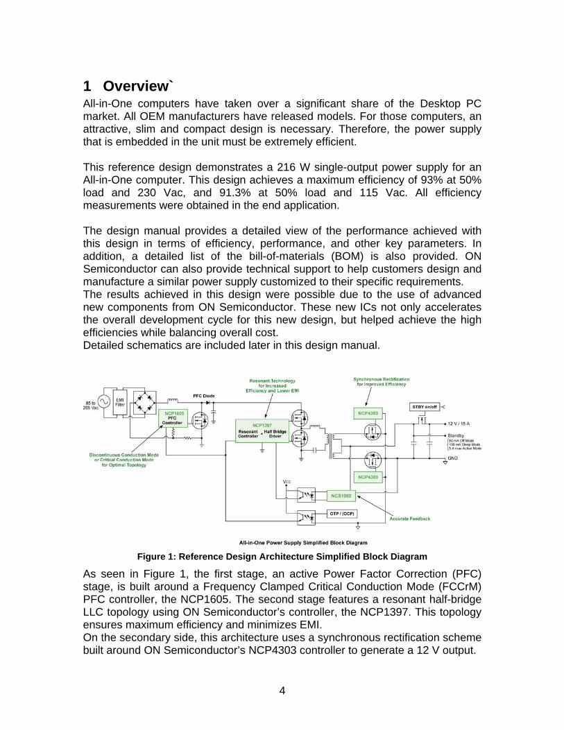
1 Overview` All-in-One computers have taken over a significant share of the Desktop PC market. All OEM manufacturers have released models. For those computers, an attractive, slim and compact design is necessary. Therefore, the power supply that is embedded in the unit must be extremely efficient. This reference design demonstrates a 216 W single-output power supply for an All-in-One computer. This design achieves a maximum efficiency of 93% at 50% load and 230 Vac, and 91.3% at 50% load and 115 Vac. All efficiency measurements were obtained in the end application. The design manual provides a detailed view of the performance achieved with this design in terms of efficiency, performance, and other key parameters. In addition, a detailed list of the bill-of-materials (BOM) is also provided. ON Semiconductor can also provide technical support to help customers design and manufacture a similar power supply customized to their specific requirements. The results achieved in this design were possible due to the use of advanced new components from ON Semiconductor. These new ICs not only accelerates the overall development cycle for this new design, but helped achieve the high efficiencies while balancing overall cost. Detailed schematics are included later in this design manual.
Figure 1: Reference Design Architecture Simplified Block Diagram
As seen in Figure 1, the first stage, an active Power Factor Correction (PFC) stage, is built around a Frequency Clamped Critical Conduction Mode (FCCrM) PFC controller, the NCP1605. The second stage features a resonant half-bridge LLC topology using ON Semiconductor’s controller, the NCP1397. This topology ensures maximum efficiency and minimizes EMI. On the secondary side, this architecture uses a synchronous rectification scheme built around ON Semiconductor’s NCP4303 controller to generate a 12 V output.

5
2 Specification
2.1 Efficiency requirements This reference design exceeds the 80 PLUS Silver (www.80pls.org), ENERGY STAR® 5.0 (www.energystar.gov), and Climate Savers Computing Initiative (CSCI) Step 3 (www.climatesaverscomputing.org) efficiency targets for desktop PC single-output power supplies. Table 1 hereafter shows a summary of the efficiency targets from these different organizations.
Table 1
2.2 Input Voltage • Universal input 90 Vac to 265 Vac, 47-63 Hz
2.3 Main Power Supply Output voltage: • 12 V / 15 A
Levels Specification
20% of rated
outputpower
50% of rated
outputpower
100% of rated
outputpower
Effective Date
• Single-Output• Non-Redundant• PFC 0.9 at 50%
81% 85% 81% StartJune 2007
• Single-Output• Non-Redundant• PFC 0.9 at 50%
85% 89% 85% StartJune 2008
• Single-Output• Non-Redundant• PFC 0.9 at 50%
88% 92% 88% StartJune 2010
• Single-Output• Non-Redundant• PFC 0.9 at 50%
90% 94% 91% Target
Efficiency (%)
Sing
le-O
utpu
t

6
2.4 Standby Power Supply: • 50 mA in off mode • 100 mA in sleep mode • 5 A in active mode
3 Architecture Overview The architecture selected is designed around a succession of conversion stages as illustrated in Figure 1. The first stage is a universal input, active power factor boost delivering a constant output voltage of 385 V to the second stage, the half-bridge resonant LLC converter. On the secondary side, this architecture uses a synchronous rectification scheme built around ON Semiconductor’s NCP4303 controller in order to generate a +12 V output. The semiconductor components, supporting this All in One PC reference design are the NCP1605 PFC controller, the NCP1397 half-bridge resonant controller and the NCP4303 synchronous rectification.
3.1 Primary Side: Power Factor Correction Stage ON Semiconductor offers solutions for 3 PFC operation modes:
Table 2: PFC operation modes
For a 216 W output power design, a Frequency Clamped Critical Conduction Mode (FCCrM) approach is the most suitable one because of its high efficiency and smooth EMI signature. The NCP1605 operates in this mode. The circuit also incorporates protection features for a rugged operation together with some dedicated circuitry to lower the power consumed by the PFC stage in no load conditions.
Operating Mode Main Feature
Critical conduction Mode (CrM)
Large rms currentSwitching frequency is not fixed
e.g.: NCP1606
Frequency ClampedCritical Conduction
Mode (FCCrM)
Large rms currentFrequency is limitedReduced coil inductance
e.g.: NCP1605
ContinuousConduction Mode
(CCM)
Always hard-switchingInductor value is largestMinimized rms current
e.g.: NCP1654
IL
IL
IL
TclampTclamp

7
3.2 Primary Side: Half bridge resonant LLC Converter
3.2.1 The Half Bridge Resonant LLC topology The Half Bridge Resonant LLC topology, that is a member of the Series Resonant Converters (SRC), is widely used in applications where high power density is necessary. The Half Bridge Resonant LLC converter is an attractive alternative to the traditional Half Bridge (HB) topology for several reasons. Advantages include:
• ZVS (Zero Voltage Switching) capability over the entire load range: Switching takes place under conditions of zero drain voltage, which results is nearly nearly zero turn-on losses. This improves the EMI signature compared to the HB, which operates under hard-switching conditions.
• Low turnoff current: Switches are turned off under low current conditions, lowering turn-off losses compared to the HB topology.
• Zero current turnoff of the secondary diodes: When the converter operates under full load, the output rectifiers are turned off under zero-current conditions, reducing the EMI signature.
• No increased component count: The component count is virtually the same as the classical half bridge topology.
Figure 2 shows the structure of this resonant converter. A 50 % duty-cycle half-bridge delivers high-voltage square waves swinging from 0 V to the input voltage VIN to a resonating circuit. By adjusting the frequency via a voltage-controlled oscillator (VCO), the feedback loop can adjust the output level depending on the power demand.
1
Vin
Q
Qb
6 5 7
9
Vout
RLC
N:1Ls Cs
Lm
Figure 2
The resonating circuit is made of a capacitor, Cs, in series with two inductors, Ls and Lm. One of these inductors, Lm, represents the magnetizing inductance of the transformer and creates one resonating point together with Ls and Cs. The

8
reflection of the load across this inductor will either make it disappear from the circuit (Lm is fully short-circuited by a reflected RL of low value at heavy load currents) or will make it stay in series with the inductor Ls in light load conditions. As a result, dependant on the loading conditions, the resonant frequency will move between a minimum and a maximum:
The steady state frequency of operation depends on the power demand. For a low power demand, the operating frequency is rather high, away from the resonating point. On the contrary, at high power, the switching frequency decreases approaching resonant frequency to deliver the necessary amount of current to the load. This topology behaves like a frequency dependent divider.
Figure 3: Substitutive schematic of the LLC resonant converter
ηπ ⋅⋅⋅
= 22
8nRR L
ac
Where: RL is the real loading resistance n is the transformer turns ratio η is the expected efficiency
3.2.2 LLC elements used in the reference design • Transformer:
o Primary inductance Lm= 430 uH o Leakage inductance Llk= 55 uH o Turn ratio primary to secondary n = 17.5 o Turn ratio primary to auxiliary naux = 11.6
• Resonant coil: Ls= 30 uH • Resonant capacitor: Cs= 2 x 12 nF

9
3.2.3 LLC Gain Characteristics
0.000
0.010
0.020
0.030
0.040
0.050
0.060
0.070
0.080
0.090
0.100
1.00E+04 1.00E+05 1.00E+06
Frequency [Hz]
Gai
n [-]
Full load
fop= 87 kHz@ Vbulk=350 Vdc fop= 103 kHz@ Vbulk=385 Vdc
fop= 124 kHz@ Vbulk=420 Vdc
Figure 4: Gain Characteristics
Please note that the selected resonant tank provides narrow operating frequency range.
3.2.4 LLC Controller: NCP1397 The heart of the half-bridge resonant LLC converter stage is the NCP1397. Thanks to its proprietary high-voltage technology, this controller includes a bootstrapped MOSFET driver for half-bridge applications that accept bulk voltages up to 600 V. Multiples protections (e.g. immediate shutdown or timer-based event, brownout, broken optocoupler detection, etc), contribute to a safer converter design, without additional complex circuit. An adjustable dead time also helps lower the shoot-through current contribution as the switching frequency increases.
3.2.5 More information More information about LLC structure can be found in the ON Semiconductor application note AND8311/D (Understanding the LLC Structure in Resonant Applications).
3.3 Secondary Side: Synchronous Rectification
3.3.1 Why Synchronous Rectification Figure 5 highlights the benefits of using synchronous rectification at higher output current compared to the standard approach of using diodes.

10
Figure 5: Synchronous Rectification benefits
Figure 5 also shows that in light load conditions, the Synchronous Rectification must be turned off. Figure 6 details how the NCP4303 is disabled when the output current is low.
Figure 6: Syn. Rectification controller is shut down when the output current is low
0
1
2
3
4
5
6
0 3 6 9 12 15 18Output current [A]
Loss
es [W
]Losses calculated for one Shottky diode
Losses calculated for one SR MOSFET (including driving)
1.4 % of output power
2.17 % of output power
2.33 % of output power
Point at which Sync Rec has advantages

11
3.3.2 Synchronous Rectification Controller: NCP4303 The 12 V output generated by the half-bridge resonant LLC converter is rectified using a proprietary synchronous rectification scheme built around two NCP4303 controllers and two external single N-channel MOSFETs. Key features offered by the NCP4303:
• Operates in CCM and DCM Applications • True Secondary Zero Current Detection with Adjustable Threshold • Automatic Parasitic Inductance Compensation • 50 ns Turn off Delay from CS to Driver • Interface to External Signal for CCM Mode • Trigger Input to enter Standby Mode • Adjustable Min Ton Independent of Vcc Level • Adjustable Min Toff Independent of Vcc Level • 5 A / 2.5 A Peak Current Drive Capability • Voltage range up to 30 V (Gate drive clamp of either 12 V or 5 V) • Low startup and standby current consumption

12
4 Performance Results
4.1 Total Efficiency
808182838485868788899091929394
0 3 6 9 12 15 18Output current [A]
Effic
ienc
y [%
]
230 110
Figure 7: Efficiency Measurements
Total Efficiency 20% load 50% load 100% load
AC input Meas. Spec. Meas. Spec. Meas. Spec. Conclusion
110 VAC 89.6% 85% 91.3% 89% 89.1% 85% Passed 230 VAC 90.6% 85% 93.0% 89% 91.9% 85% Passed
Table 3: Efficiency results
4.2 Light load Efficiency
4.2.1 Discharging X2 Capacitors Achieving the lowest possible standby power is one of the goals of this reference design. X2 capacitors are used to minimize the conducted EMI signature of the power supply. For safety reasons, it is mandatory to discharge those capacitors once the application is unplugged. Often resistors perform this function. This result in power always being dissipated, it significantly alters the efficiency of the power supply in light load condition. In this reference design, dedicated circuitry has been used to improve this power loss (see Figure 8). The capacitor C3 is discharged via R5 and R6 that are only connected when the mains is gone and when Q6 is turned on.

13
Figure 8: an efficient way to discharge X2 capacitors
4.2.2 Results
0
200
400
600
800
1000
1200
1400
1600
1800
2000
90 115 140 165 190 215 240 265AC voltage [V]
Con
sum
ptio
n [m
W]
No load50 mA load
Figure 9: Light load efficiency measurements

14
5 Detail losses distribution
0
1
2
3
4
5
6
7
8
9
Output
switc
h
LLC M
OSFETs
Reson
ant c
oil
PFC coil
Bridge
rect.
Transfo
rmer
PFC sw. &
diod
e
SR recti
fier
Pd [W
]
Vin=110 VacVin=230 Vac
Figure 10: Losses Distributions
5.1 Power Factor Power Factor
AC input 20% load 50% load 100% load Specification Conclusion
110 VAC 0.954 0.984 0.992 Passed
230 VAC 0.756 0.881 0.940
PF > 0.9 @ 100% and 50 % of
rated output power
Passed
Table 4

15
6 Board Picture
Resonant inductor
Transformer
SR MOSFETsand STBY switch on cooler
Output connector
Secondarycapacitor
PFC stage
LLC stage
EMI filter
NCP1605 PFC cnt. NCP1397B LLC cnt.
2 x NCP4303 SR cnt.
NCS1002 regulator
LM324 amplifier

16
7 Schematic
Figure 11: Power Supply Schematic

17
8 Board Layout
Figure 12: PCB top side

18
Figure 13: Top side components

19
Figure 14: PCB bottom side

20
Figure 15: Bottom side components

21
9 Board Part list Parts Qty Value Device
B1 1 KBU8R BRIDGE RECTIFIER
C1, C3 2 22u ELECTROLYTIC CAPACITOR
C10 1 120u ELECTROLYTIC CAPACITOR
C11, C29 2 1u CERAMIC CAPACITOR C13 1 820n CERAMIC CAPACITOR
C14, C34, C38, C44, C48, C52, C57, C58, C60, C69 10 100n CERAMIC CAPACITOR C15 1 1u CERAMIC CAPACITOR
C16, C17 2 22n CERAMIC CAPACITOR C2 1 1n CERAMIC CAPACITOR
C20, C21, C22, C23, C24, C25, C26 7 470uF/16V ELECTROLYTIC CAPACITOR
C27, C66 2 220n CERAMIC CAPACITOR C28, C67 2 22n CERAMIC CAPACITOR
C31 1 330n CERAMIC CAPACITOR C35 1 220p CERAMIC CAPACITOR
C36, C43 2 100p CERAMIC CAPACITOR
C4 1 10u/50V ELECTROLYTIC CAPACITOR
C40 1 6.8n CERAMIC CAPACITOR C42 1 470n X2 CAPACITOR
C46, C47 2 470n CERAMIC CAPACITOR C49 1 47p CERAMIC CAPACITOR
C5, C32 2 33n CERAMIC CAPACITOR C50 1 560p CERAMIC CAPACITOR C51 1 10n CERAMIC CAPACITOR
C53 1 220u/25 ELECTROLYTIC CAPACITOR
C54, C55 2 10u/15V CERAMIC CAPACITOR C56, C65 2 2n2 CERAMIC CAPACITOR
C59 1 47n CERAMIC CAPACITOR C6, C7, C19 3 1u POLYESTER CAPACITOR
C63 1 1uF CERAMIC CAPACITOR
C64 1 4u7/35V ELECTROLYTIC CAPACITOR
C68 1 100n CERAMIC CAPACITOR

22
C8, C39 2 3n9 CERAMIC CAPACITOR C9, C18 2 12n CERAMIC CAPACITOR
CY1 1 2n2/Y1 Y1 CAPACITOR D1, D2, D7, D11, D19, D20, D26, D30 8 MMSD4148 DIODE
D12 1 MM3Z18VT1G ZENER DIODE D14 1 MMSZ5236BT1G ZENER DIODE
D22, D23, D31, D33, D34, D35 6 NSR0340HT1G DIODE D3 1 M1MA142WKT1G DOUBLE DIODE D32 1 MURA160 DIODE D4 1 1N5408 DIODE D5 1 MMSZ16 ZENER DIODE D6 1 MURF550MFG DIODE
D8, D21 2 12CWQ06FNDPAK DOUBLE DIODE D9, D13, D17 3 MRA4007 DIODE
F1 1 5A FUSE IC1, IC2 2 NCP4303A SR CONTROLLER
IC3 1 NCP1605 PFC CONTROLLER IC4 1 NCS1002 CV/CC CONTROLLER IC5 1 LM358D OPERATION AMPLIFIER IC6 1 NCP1397B RESONANT CONTROLLER IC7 1 TLV431 VOLTAGE REFERENCE L1 1 200uH INDUCTOR
L2, L4 2 INDUCTOR L3 1 30uH INDUCTOR
L5 1 82721A COMMON MODE INDUCTOR
L6, L7 2 70nH INDUCTOR OK1, OK2 2 PC817 TRANSISTOR
Q1, Q2, Q14, Q16 4 BC846A TRANSISTOR Q10 1 BC807-16L TRANSISTOR
Q11, Q15 2 IRFB3206 N-MOSFET Q4 1 IPP20N60 N-MOSFET
Q5, Q12 2 STP12NM50FP N-MOSFET Q6 1 MPSA44 TRANSISTOR Q7 1 BC856B TRANSISTOR Q8 1 15N04N N-MOSFET
Q9, Q13 2 2N7002E MOSFET R1, R9, R15, R57 4 22R RESISTOR SMD
R103 1 62k RESISTOR SMD

23
R105 1 24k RESISTOR SMD R106 1 200R RESISTOR SMD R108 1 560k RESISTOR SMD
R11, R12, R22, R23, R37, R38, R55, R56 8 1.8M RESISTOR SMD R110, R111 2 6k8 RESISTOR SMD
R114 1 2.7k RESISTOR SMD R116 1 27k RESISTOR SMD R117 1 2.2k RESISTOR SMD R123 1 18R RESISTOR SMD R126 1 22k RESISTOR SMD R127 1 9.1k RESISTOR SMD
R13, R20 2 220 HV RESISTOR SMD R135, R141 2 7.5k RESISTOR SMD
R137 1 330 RESISTOR SMD R142 1 200k RESISTOR SMD
R16, R25, R36 3 1M8 RESISTOR SMD R18 1 220k RESISTOR SMD
R19, R90 2 27R RESISTOR SMD R2, R42, R45, R69, R70, R86, R87, R95, R121, R122, R125, R130, R144,
R145 14 1k RESISTOR SMD
R21 1 33R RESISTOR SMD R24, R109, R124, R133 4 5.6k RESISTOR SMD
R26 1 1k RESISTOR SMD R27 1 2R2 RESISTOR SMD
R28, R80, R81 3 10R RESISTOR SMD R29, R120 2 47k RESISTOR SMD
R3, R17 2 100R RESISTOR SMD R30, R33, R35, R39, R48, R51, R52, R71, R76, R77, R107, R113, R148 13 10k RESISTOR SMD
R31, R91 2 56k RESISTOR SMD R34, R67 2 16k RESISTOR SMD R4, R100 2 100k RESISTOR SMD R40, R59 2 0R RESISTOR SMD
R41 1 20k RESISTOR SMD R43 1 470 RESISTOR SMD R46 1 0.1R RESISTOR R47 1 10 RESISTOR-SMD
R5, R14 2 47k HV RESISTOR SMD R50 1 51R RESISTOR-SMD

24
R53 1 8.2k RESISTOR-SMD R54, R134, R138 3 6.2k RESISTOR-SMD
R58 1 7k5 RESISTOR-SMD R6, R49 2 4.7R RESISTOR-SMD
R60 1 1M8 RESISTOR-SMD R61 1 0R002 RESISTOR-SMD
R62, R79 2 22k RESISTOR-SMD R63 1 47R RESISTOR-SMD
R64, R132 2 10k@25deg THERMISTOR R65, R66 2 4R7 RESISTOR-SMD
R7 1 4M7 RESISTOR R73 1 1k RESISTOR-SMD R74 1 5k6 RESISTOR-SMD
R75, R112, R140 3 22k RESISTOR-SMD R78, R139 2 150k RESISTOR-SMD
R8 1 330R RESISTOR-SMD R82 1 430k RESISTOR-SMD R83 1 51k RESISTOR-SMD R85 1 18k RESISTOR-SMD
R92, R147 2 13k RESISTOR-SMD R94, R97, R136 3 15k RESISTOR-SMD
R96, R146 2 330k RESISTOR-SMD R98 1 6.8k RESISTOR-SMD
R99, R128 2 43k RESISTOR-SMD TR1 1 TRANSFORMER

25
10 Resources/Contact Information Data sheets, applications information and samples for the ON Semiconductor components are available at www.onsemi.com. Links to the datasheets of the main components used in this design are included in the Appendix. Authors of this document are Jaromir Uherek, Roman Stuler and Christophe Warin
11 Appendix
11.1 Link to ON Semiconductor’s web site • ON Semiconductor Home Page
11.2 Industry information links: • ENERGY STAR • 80 PLUS Efficiency Requirements • Climate Savers Computing Initiative • IEC61000-3-2 Requirements • European Union (EU) Energy Star Page
11.3 Additional collateral from ON Semiconductor • NCP1605: Enhanced, High Voltage and Efficient Standby Mode PF Controller • NCP1397: High Perf. Resonant Mode Controller with Integrated High Voltage Drivers • NCP4303: Secondary Side Synchronous Rectification Driver • TLV431: Low Voltage Precision Adjustable Shunt Regulator • NCS1002: CV/CC Secondary Controller • LM358D: Single Supply Dual Operational Amplifier
11.4 Other ON Semiconductor Discrete Products • MMSD4148 • MM3Z18VT1G • MMSZ5236BT1G • NSR0340HT1G • M1MA142WKT1G • MURA160 • 1N5408 • MMSZ16 • MURF550MFG • MRA4007 • BC846A • BC856
BC807-16L