2.1 Modular Microoptical Systems for Sensors and ...
32
2.1 Modular Microoptical Systems for Sensors and Telecommunication U. Wallrabe and J. Mohr, Forschungszentrum Karlsruhe, Karlsruhe, Germany Abstract This paper focuses on fabrication and assembly processes of modular and hybrid microoptical systems in use in sensor and telecommunica- tion fields. These microoptical systems are made by a huge variety of processes, which are commonly known as microsystem technology. Nevertheless, quite a lot of them are based on the LIGA process, since LIGA is an “assembly friendly” technology. Modular microoptical systems typically comprise several functions incorporating mechanical or electromechanical components beside the optical elements. The assembly of the diverse submounts and compo- nents is performed actively as well as passively. In many cases, all of these functions can be combined on one single chip. In several cases, however, a pair of chips, which is assembled in a flip-chip like way, is used. The framework of the paper leads to a definition of the terminus “modular microoptical system” and argues for the advantages of such a modular design approach. It closes with some remarks on automatic assembly strategies. Keywords: microoptics; modular; hybrid; flip-chip; assembly Contents 2.1.1 Introduction ......................................... 144 2.1.2 Definition of a Modular Microoptical System .................. 145 2.1.3 Optomechanical Systems ................................ 146 2.1.3.1 Fiber Coupler in Silicon with Rhombus-like Grooves ............. 147 2.1.3.2 Easy-assembly Fiber Coupler from Polymer ................... 148
Transcript of 2.1 Modular Microoptical Systems for Sensors and ...

2.1 Modular Microoptical Systemsfor Sensors and Telecommunication
���������� and � ��� Forschungszentrum Karlsruhe, Karlsruhe,Germany
Abstract
This paper focuses on fabrication and assembly processes of modularand hybrid microoptical systems in use in sensor and telecommunica-tion fields. These microoptical systems are made by a huge variety ofprocesses, which are commonly known as microsystem technology.Nevertheless, quite a lot of them are based on the LIGA process, sinceLIGA is an “assembly friendly” technology.
Modular microoptical systems typically comprise several functionsincorporating mechanical or electromechanical components beside theoptical elements. The assembly of the diverse submounts and compo-nents is performed actively as well as passively. In many cases, all ofthese functions can be combined on one single chip. In several cases,however, a pair of chips, which is assembled in a flip-chip like way, isused.
The framework of the paper leads to a definition of the terminus“modular microoptical system” and argues for the advantages of sucha modular design approach. It closes with some remarks on automaticassembly strategies.
Keywords: microoptics; modular; hybrid; flip-chip; assembly
Contents
2.1.1 Introduction . . . . . . . . . . . . . . . . . . . . . . . . . . . . . . . . . . . . . . . . . 144
2.1.2 Definition of a Modular Microoptical System . . . . . . . . . . . . . . . . . . 145
2.1.3 Optomechanical Systems . . . . . . . . . . . . . . . . . . . . . . . . . . . . . . . . 1462.1.3.1 Fiber Coupler in Silicon with Rhombus-like Grooves . . . . . . . . . . . . . 1472.1.3.2 Easy-assembly Fiber Coupler from Polymer . . . . . . . . . . . . . . . . . . . 148

2.1.3.3 Expanded Beam Fiber Coupler . . . . . . . . . . . . . . . . . . . . . . . . . . . . 149
2.1.4 Opto-electromechanical Systems 1: Optical Benches Combinedwith Electrooptical Components . . . . . . . . . . . . . . . . . . . . . . . . . . . 151
2.1.4.1 Heterodyne Receiver . . . . . . . . . . . . . . . . . . . . . . . . . . . . . . . . . . . 1512.1.4.2 Spectrometer . . . . . . . . . . . . . . . . . . . . . . . . . . . . . . . . . . . . . . . . 1532.1.4.3 Distance Sensor . . . . . . . . . . . . . . . . . . . . . . . . . . . . . . . . . . . . . . 1542.1.4.4 Blood Flow Sensor . . . . . . . . . . . . . . . . . . . . . . . . . . . . . . . . . . . . 155
2.1.5 Opto-electromechanical Systems 2: Optical Benches Combinedwith Electrooptical Components and Actuators . . . . . . . . . . . . . . . . . 157
2.1.5.1 Segmented Deformable Mirror . . . . . . . . . . . . . . . . . . . . . . . . . . . . 1582.1.5.2 Optical Cross Connect with Linear Motion Actuated by Electrostatics . 1592.1.5.3 Optical Cross Connect with Vertical Motion Generated
by Piezo Actuators . . . . . . . . . . . . . . . . . . . . . . . . . . . . . . . . . . . . 1602.1.5.4 Optical Cross Connect with Rotating Mirrors Actuated by Electrostatics 1622.1.5.5 Oscillating Modulator for Infrared Light Actuated by Electromagnetics 1642.1.5.6 Laser Scanner for Barcode Reading Actuated by Electromagnetics . . . 166
2.1.6 A Final Word About Assembly Technology . . . . . . . . . . . . . . . . . . . 167
2.1.7 Conclusions . . . . . . . . . . . . . . . . . . . . . . . . . . . . . . . . . . . . . . . . . 172
2.1.8 References . . . . . . . . . . . . . . . . . . . . . . . . . . . . . . . . . . . . . . . . . . 173
2.1.1 Introduction
The tremendous increase in demand for rapid information and communicationhas pushed light to the number one data transfer medium. The great advantagesof light are not only its unique velocity but also its insensitivity to disturbancebecause the photons do not interact either with external fields or with them-selves. This makes light a very attractive medium to transfer information, espe-cially across long distances but also on short stretches. The percentage of infor-mation that is already transferred by light through optical fiber networks differsfrom country to country. In Germany, for example, it has already reached 90%since investigations started quite early in this promising technology [1]. Recentinterest in optical telecommunications lies not only in global networks, but alsoin private households [2] and in cars [3]. Hence optical components that enterthe consumer market are subject to increased price pressure.
Similar arguments are valid for optical sensors. Again, the insensitivity to dis-turbance is the main reason for the increasing application of optical sensors incars and industrial production for control and monitoring of automatic processes.Also in medical technology, optical sensors are of great interest because they aremostly non-invasive and can be used in the proximity of strong fields, eg, closeto the magnetic field of a nuclear resonance tomograph [4].
Striving for cost reduction through higher integration and on-going miniaturi-zation, the field of micro optics becomes an enabling technology for optical tele-
144 2.1 Modular Microoptical Systems for Sensors and Telecommunication
communication and sensors. There are two basic technology approaches: a fullyintegrated fabrication sequence or a modular or hybrid set-up. The choice ofwhich one is the most suitable is related to the number of pieces to be fabri-cated, the complexity of available processes and the respective yield, and thefreedom in design and construction. Each approach has its specific advantages.In case of lower numbers and for the combination of several functional compo-nents, the modular design and fabrication is often the better choice. The pro-cesses are easier and safer, and one can work with pre-tested components, whichhelps to enhance the yield.
This chapter concentrates on micro optical systems for telecommunication andsensors that follow the modular approach, in addition based on micro electro me-chanical system (MEMS) or micro opto electro mechanical system (MOEMS)techniques. Examples for diverse purposes will be presented.
2.1.2 Definition of a Modular Microoptical System
The definition of the expression ‘modular microoptical system’ as it will be un-derstood in this paper is best done in the reverse direction. An ‘optical system’comprises a variety of functions in one unit: optical function and normally elec-trical and/or mechanical function. Examples of pure optical function are simplylight transfer, refraction and diffraction, imaging, filtering, light splitting orsuperposition. Electrical or optoelectrical function can be light generation, detec-tion or analysis, electronic circuitry, or current/voltage supply to other functionalcomponents. Mechanical or electromechanical function is provided by alignmentstructures or positioning aids, fixing and clamping structures, actuators, heatersand coolers.
Such an optical system is called ‘micro’ when at least one component of it isfabricated by means of micro-technology. The overall size of the system or evenof the diverse components is not necessarily in the range of micrometers, butmaybe some structural detail calls for micro-technology. A huge variety of suchmicrooptical systems have been presented in recent years. These can simply befiber couplers [5] or beam splitters [6], or more complex devices as switchablemirrors [7, 8], fiber switches [9, 10], Fabry-Perrot interferometers [11], or modu-lators [12].
A microoptical system is defined as ‘modular’ or sometimes just ‘hybrid’ ifthe diverse functions are not fabricated in one common fully integrated fabrica-tion sequence and/or if they are not integrated on the same substrate. An opticalbench, eg, fabricated with an adapted process on one substrate, and an actuator,which is fabricated with another specific process on a second substrate, form twomodules, which are finally put together. In addition, the components required foreach module can be fabricated separately and mounted in a hybrid way. It isclear that the definition of ‘modular’ and ‘hybrid’ cannot be used rigidly. In gen-
A2.1.2 Definition of a Modular Microoptical System 145

eral, the individual scientist decides whether he or she considers a system justdeveloped already to be a modular or just a hybrid set-up. Also in this chapter,we did not succeed in separating them. Hence modular and hybrid systems willnecessarily be mixed up or even lead to contradictory points of view. We willstress this aspect in Section 2.1.5, which describes the most complex modularsystems in this chapter.
Anyhow, no matter what name it is given, a modular or hybrid microopticalsystem is always related to assembly technology comprising alignment and fixa-tion [13]. This can be performed either actively or passively. Active alignmentmeans that the output signal of the system is monitored during assembly in orderto obtain an optimum result. Passive assembly, in contrast, makes use of inte-grated alignment aids for the diverse components without the need for monitor-ing. The question of which method is the most suitable needs to be answered foreach system separately. It is dependent on the function of the system and on theavailable fabrication and assembly procedures.
The examples of modular microoptical systems that are given in the followingsections are split into three categories. The first covers pure opto-mechanical sys-tems without any need for electrical units. The second covers opto-electro-me-chanical systems in which the electrical units are responsible for light generationand detection. The third also describes opto-electro-mechanical systems, but in-cluding electrically driven actuators. In order not to overload this chapter, onlythe modular concepts and operating principles of the systems will be explained.For detailed results we refer to the original publications.
2.1.3 Optomechanical Systems
Pure optomechanical modular systems can hardly be found. Again, the boundarybetween a monolithic, integrated system and a hybrid, modular system is float-ing. This becomes clear from consideration of an optical bench with non-inte-grated but assembled microoptical components. The base plate of an opticalbench mostly is a monolithic device with alignment aids and perhaps some inte-grated devices such as a prism or a mirror. When additional components such asfibers, lenses, beam splitters, etc., are assembled on the bench it becomes a sys-tem according to the definition above. A very simple example is a fiber coupleras used for telecommunication purposes with the optical function of guidinglight from one fiber to the next and the mechanical function of alignment andfixation. Three different approaches to fiber couplers are presented in the follow-ing discussion.
146 2.1 Modular Microoptical Systems for Sensors and Telecommunication

2.1.3.1 Fiber Coupler in Silicon with Rhombus-like Grooves
Fibers are commonly aligned by grooves on a chip running parallel to the fiberaxis or they are pushed through holes in a chip mounted perpendicular to thefiber axis. Most popular are V-grooves etched in single crystal silicon [14]. Thefibers are fixed by glue and covered with a glass plate. A newer approach is touse rhombus-shaped channels [15] as indicated in Figure 2.1.1. The grooves al-low for lateral and vertical positioning of the fibers. The authors claim two ad-vantages over simple V-grooves. First, the volume of the rhombus is smaller, thusreducing the amount of glue which is necessary. This again reduces shear stressin the whole assembly of the Si chip, the cover glass plate, the fibers, and theglue owing to the different thermal expansion when temperature changes occur.Second, fiber assembly is very easy because funnels are generated owing to theetching process at the edges of the chip. The fibers are inserted at the wide end
A2.1.3 Optomechanical Systems 147
Figure 2.1.1. Comparison of fiber grooves with triangular and rhombus-like shapes [15](with permission of Springer-Verlag).
Figure 2.1.2. Rhombus-like channel with funnel at the end etched in silicon and fiber as-sembled in channel [15] (with permission of Springer-Verlag).
of the funnels, and as they are pushed forward they center by themselves (Figure2.1.2). The end face is finally prepared with a wafer saw.
2.1.3.2 Easy-assembly Fiber Coupler from Polymer
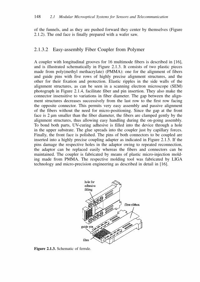
A coupler with longitudinal grooves for 16 multimode fibers is described in [16],and is illustrated schematically in Figure 2.1.3. It consists of two plastic piecesmade from poly(methyl methacrylate) (PMMA): one for the alignment of fibersand guide pins with five rows of highly precise alignment structures, and theother for their fixation and protection. Elastic ripples in the side walls of thealignment structures, as can be seen in a scanning electron microscope (SEM)photograph in Figure 2.1.4, facilitate fiber and pin insertion. They also make theconnector insensitive to variations in fiber diameter. The gap between the align-ment structures decreases successively from the last row to the first row facingthe opposite connector. This permits very easy assembly and passive alignmentof the fibers without the need for micro-positioning. Since the gap at the frontface is 2 �m smaller than the fiber diameter, the fibers are clamped gently by thealignment structures, thus allowing easy handling during the on-going assembly.To bond both parts, UV-curing adhesive is filled into the device through a holein the upper substrate. The glue spreads into the coupler just by capillary forces.Finally, the front face is polished. The pins of both connectors to be coupled areinserted into a highly precise coupling adapter as indicated in Figure 2.1.5. If thepins damage the respective holes in the adaptor owing to repeated reconnection,the adaptor can be replaced easily whereas the fibers and connectors can bemaintained. The coupler is fabricated by means of plastic micro-injection mold-ing made from PMMA. The respective molding tool was fabricated by LIGAtechnology and micro-precision engineering as described in detail in [16].
148 2.1 Modular Microoptical Systems for Sensors and Telecommunication
Figure 2.1.3. Schematic of ferrule.

2.1.3.3 Expanded Beam Fiber Coupler
A comparable connector concept is reported in [17]. The authors also describean injection molded coupler for which the tool was made in a similar way; how-ever, the precision fiber grooves are obtained by V-grooves etched in silicon.They extended this concept to an expanded beam coupler [18] with the advan-tage of decreased sensitivity to fiber misalignment and to impurities. In that casethe fibers are not coupled face to face but lens arrays are placed between themin order to expand the light beam for coupling and refocus it again into the out-put fibers as sketched in Figure 2.1.6. For this purpose, lens alignment structuresare positioned in front of the V-grooves. Figure 2.1.7 shows the front face of
A2.1.3 Optomechanical Systems 149
Figure 2.1.4. SEM of alignment structures.
Figure 2.1.5. Pair of ferrules with coupling adapter.

150 2.1 Modular Microoptical Systems for Sensors and Telecommunication
Figure 2.1.6. Principle of an expanded beam fiber coupler [18] (with permission ofSPIE).
Figure 2.1.7. Front view of a molded expanded beam coupler with alignment structuresfor a lens array [18] (with permission of SPIE).
Figure 2.1.8. Assembled coupler with lens array, guide pins, and fiber ribbon [18] (withpermission of SPIE).
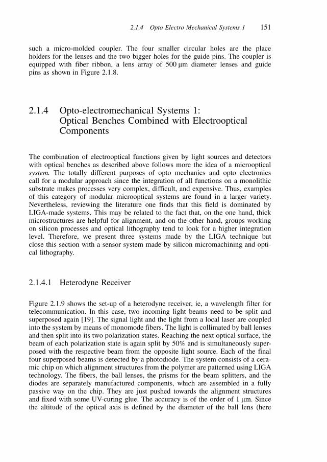
such a micro-molded coupler. The four smaller circular holes are the placeholders for the lenses and the two bigger holes for the guide pins. The coupler isequipped with fiber ribbon, a lens array of 500 �m diameter lenses and guidepins as shown in Figure 2.1.8.
2.1.4 Opto-electromechanical Systems 1:Optical Benches Combined with ElectroopticalComponents
The combination of electrooptical functions given by light sources and detectorswith optical benches as described above follows more the idea of a microopticalsystem. The totally different purposes of opto mechanics and opto electronicscall for a modular approach since the integration of all functions on a monolithicsubstrate makes processes very complex, difficult, and expensive. Thus, examplesof this category of modular microoptical systems are found in a larger variety.Nevertheless, reviewing the literature one finds that this field is dominated byLIGA-made systems. This may be related to the fact that, on the one hand, thickmicrostructures are helpful for alignment, and on the other hand, groups workingon silicon processes and optical lithography tend to look for a higher integrationlevel. Therefore, we present three systems made by the LIGA technique butclose this section with a sensor system made by silicon micromachining and opti-cal lithography.
2.1.4.1 Heterodyne Receiver
Figure 2.1.9 shows the set-up of a heterodyne receiver, ie, a wavelength filter fortelecommunication. In this case, two incoming light beams need to be split andsuperposed again [19]. The signal light and the light from a local laser are coupledinto the system by means of monomode fibers. The light is collimated by ball lensesand then split into its two polarization states. Reaching the next optical surface, thebeam of each polarization state is again split by 50% and is simultaneously super-posed with the respective beam from the opposite light source. Each of the finalfour superposed beams is detected by a photodiode. The system consists of a cera-mic chip on which alignment structures from the polymer are patterned using LIGAtechnology. The fibers, the ball lenses, the prisms for the beam splitters, and thediodes are separately manufactured components, which are assembled in a fullypassive way on the chip. They are just pushed towards the alignment structuresand fixed with some UV-curing glue. The accuracy is of the order of 1 �m. Sincethe altitude of the optical axis is defined by the diameter of the ball lens (here
A2.1.4 Opto Electro Mechanical Systems 1 151

900 �m), a fiber with a diameter of only 125 �m needs to be levered to the sameheight. This is obtained by a fiber mount as becomes clear from Figure 2.1.10.The electrical connection of the diodes is done with gold tracks, which were pre-patterned on the substrate by optical lithography and wet etching.
152 2.1 Modular Microoptical Systems for Sensors and Telecommunication
Figure 2.1.9. Set-up of heterodyne receiver.
Figure 2.1.10. Fiber mount levelling the fiber on the optical axis defined by the ball lens.
2.1.4.2 Spectrometer
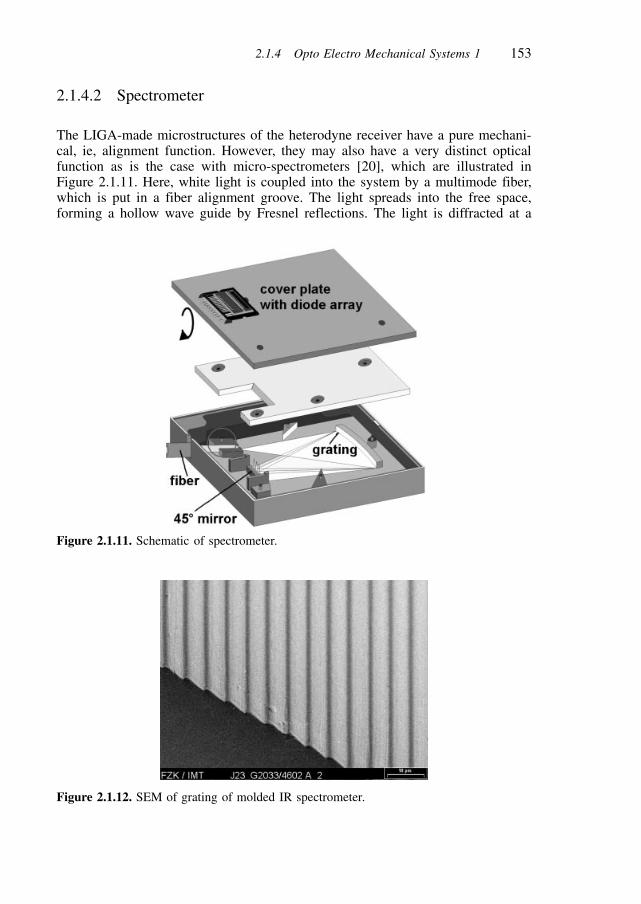
The LIGA-made microstructures of the heterodyne receiver have a pure mechani-cal, ie, alignment function. However, they may also have a very distinct opticalfunction as is the case with micro-spectrometers [20], which are illustrated inFigure 2.1.11. Here, white light is coupled into the system by a multimode fiber,which is put in a fiber alignment groove. The light spreads into the free space,forming a hollow wave guide by Fresnel reflections. The light is diffracted at a
A2.1.4 Opto Electro Mechanical Systems 1 153
Figure 2.1.11. Schematic of spectrometer.
Figure 2.1.12. SEM of grating of molded IR spectrometer.

reflection grating (Figure 2.1.12), and is coupled out of the system at a 45 � mir-ror next to the fiber. The fiber groove, the grating, and the 45 � mirror are fabri-cated in one step by hot embossing techniques [21] using a molding tool madeby LIGA technology. The polymer typically used for hot embossing is PMMA.Hence a gold layer needs to be sputtered on the PMMA structures to make themreflective. A cover plate seals the spectrometer and serves also as the upper sur-face of the hollow wave guide. An electrooptical chip with a photodiode arrayand analog electronics is finally put head-over on top of the spectrometer. Thefull system with the size of a match box is displayed in Figure 2.1.13.
2.1.4.3 Distance Sensor
A similar idea of a hybrid assembly was used for a micro-distance sensor work-ing on the basis of the triangulation principle [22], ie, the position of the spot onthe sensor’s detector is dependent on the distance of the object to be measured.As with the spectrometer, the distance sensor is divided into two functional units:a passive optical chip again fabricated by LIGA technology including bentmirrors, 45 � mirrors, and alignment structures for cylindrical lenses (Figure2.1.14a), and an electrooptical chip (Figure 2.1.14b) with a laser, a photodiodeand a position-sensitive detector (PSD). The optical components on the LIGAchip are made from PMMA covered with an evaporated gold layer. Both chipsare again mounted head-over to form an opto-electro-mechanical sensor system.For easy assembly, two micro-spheres of glass are used as position aligners ofthe LIGA and the Si chip (Figure 2.1.14c). First, the micro-spheres are placedinto pyramidal grooves on the Si base, thus centering themselves. Then, the opti-cal chip with two cylindrical holes for the spheres is passively aligned on the Sichip. The two chips before the head-over assembly are shown in Figure 2.1.15.The Si chip is already mounted on a carrier in a TO8 housing.
154 2.1 Modular Microoptical Systems for Sensors and Telecommunication
Figure 2.1.13. Full spectrometer system.

2.1.4.4 Blood Flow Sensor
Not only LIGA structures provide the advantage of optical function in parallelwith alignment accuracy. Another good example is a non-invasive blood flowsensor that makes use of the Doppler method [23]. Once again, the device is anassembly of two chips [24], as can be seen in Figure 2.1.16: one Si chip with V-grooves serves as a protection cap for the lower chip, which is an Si substratewith a polyimide waveguide, a laser diode (LD), a photodiode (PD) and elec-trodes on top of it. The Si substrate was patterned with terraces, Au/Pt/Ti elec-
A2.1.4 Opto Electro Mechanical Systems 1 155
a) b)
c)
Figure 2.1.14. (a) Passive optical chip; (b) electrooptical Si chip; (c) head-over assemblyof opto-electro-mechanical distance sensor system [22] (with permission of Springer-Ver-lag).
cylinderlenses
glasspheres
laserdiode
photo-diode

trodes, AuSn solder layers, and a three-layer polyimide waveguide. The convex-shaped edge of the waveguide collimates the light from the edge-emitting laserin the horizontal direction, thus allowing operation without the need for an addi-tional lens. Figure 2.1.17 shows a close-up view of the front face of the chippackage and the fully assembled sensor system, which is only 20 mm long.
156 2.1 Modular Microoptical Systems for Sensors and Telecommunication
Figure 2.1.15. Photograph of two chips before final assembly [22] (with permission ofSpringer-Verlag).
Figure 2.1.16. Schematic set-up of blood flow sensor and photograph of the Si substrate[24] (with permission of IEEE).

2.1.5 Opto-electromechanical Systems 2:Optical Benches Combined with ElectroopticalComponents and Actuators
In contrast to the preceding section, the idea of a system is now extended by theinclusion of actuators. Again, a modular set-up has the advantage of much easierprocesses and gives rise to more degrees of freedom for linear movement, rota-tion, and tilting. Also, the kind of actuation is easier to choose among electro-statics, electromagnetics, piezoelectric or thermal effects, or even hydraulic pres-sure or capillary forces. The choice of actuation principle is dependent on the re-quired displacement or angle as a function of the force, on boundary conditionssuch as the available driving current or voltage, the allowed temperature rise, orthe environmental conditions in the working area.
This category of opto-electro-mechanical systems is dominated by applicationsfrom the telecom field. Although a huge number of publications are concernedwith fully integrated systems, there are also some dealing with a modular set-up.No matter whether scanners or switches for fiberoptical networks are discussed,the main focus is put on steerable mirrors. The six systems presented in this sec-
A2.1.5 Opto-electromechanical Systems 2 157
Figure 2.1.17. Close-up of front face of chip package and fully assembled sensor [24](with permission of IEEE).

tion exemplify the variety of kinds of motion and actuation principles. In addi-tion, they represent diverse levels of the modular approach. As already men-tioned in the Introduction, we will use the modular microoptical systems of thissection to discuss the definition ‘modular’ once more, now with practical exam-ples.
2.1.5.1 Segmented Deformable Mirror
As in the previous section, a flip-chip-like assembly concept was used for a seg-mented deformable micromirror array for free-space optical communication as isexplained in Figure 2.1.18 [25]. The upper chip contains on its top surface seg-mented mirrors, which are attached to actuator segments, each of which is sus-pended from four cantilevers in order to pull them down. The lower chip con-tains square electrodes to apply electrostatic forces to the actuators and support-ing side walls in order to bond the two chips mechanically. All functional ele-ments, ie, the mirrors, actuators, supporting side walls and electrodes, are pat-terned in polysilicon. For thermal compression bonding, gold bond pads are de-posited on top of the side walls and onto the frame of the mirror segments. Thespacing between the actuators and electrodes is about 5 �m, which results in dis-placements of the mirrors of 1 �m at a voltage of 200 V. An SEM photograph ofone pixel of the assembled device is shown top-down in Figure 2.1.19. Part ofthe mirror has been broken off to show the underlying actuator and electrodes.
This concept easily allows one to create large mirror arrays such as1000×1000 pixels and to put the electrodes directly on integrated circuitry.Thinking on such a big scale, a single mirror is just a component of the whole
158 2.1 Modular Microoptical Systems for Sensors and Telecommunication
Figure 2.1.18. Schematic 3D drawing of a deformable micro-mirror array before and afterbonding. The vertical scale is expanded 10-fold [25] (with permission of IEEE).

system. However, on a small scale the single mirror can also be considered as asystem made of two modules: an opto mechanical (upper chip) and an electrical(lower chip) module.
2.1.5.2 Optical Cross Connect with Linear Motion Actuatedby Electrostatics
Again, flip-chip assembly was chosen for an optical fiber cross connect withMEMS switches [26] and integrated waveguides [27]. Figure 2.1.20 shows theMEMS fiber switch made by deep reactive ion etching (DRIE). It consists of twolinear electrostatic comb-like micro actuators, which generate a linear movementof the long bar in the center. The mirror (top left corner in Figure 2.1.20), whichresembles a needle in this design, is part of the bar and can move into the freespace between the grooves for the waveguides. Sixteen of these switches are ar-ranged on the substrate to form a 4 ×4 switch array as can be seen on the leftside of Figure 2.1.21. A second chip provides the integrated waveguides madefrom SiOxNy on SiO2 also patterned by DRIE. At the position of the mirrors, thewaveguides become slimmer in order to bring them as close together as possibleand thus reduce optical losses (Figure 2.1.21, right). In addition, the faces of thewaveguides can be given an optical shape. The waveguide chip is put head-overon the mechanical chip and fibers are attached to the edges of the package (Fig-ure 2.1.21, center).
In this case, the modular aspect is obvious and easy to find. The two chipshave absolutely distinct functions, one for optical waveguiding with integratedimaging, the other providing the electromechanical actuator. Hence the completesystem is an assembly of two modules.
A2.1.5 Opto-electromechanical Systems 2 159
Figure 2.1.19. SEM of a single pixel [25] (with permission of IEEE).

2.1.5.3 Optical Cross Connect with Vertical Motion Generatedby Piezo Actuators
A different approach for the realization of a 4 ×4 optical switch is described in[28]. It is a fully hybrid set-up of mostly commercial components. The principlebecomes clear from Figure 2.1.22, which shows a 1 ×4 channel system. The lightfrom the incoming fiber is collimated by miniature collimation optics. The beampasses four cantilevers with prisms on them. The cantilevers are piezoelectricbimorph actuators, which bend in the vertical direction, thus pulling the ‘non-active’ prisms below the optical axis. Depending on the position of the only ‘ac-
160 2.1 Modular Microoptical Systems for Sensors and Telecommunication
Figure 2.1.20. Flip-chip set-up of 4 ×4 optical cross connector [27] (with permission ofIEEE).
Figure 2.1.21. Close-up view of waveguides at the cross point [27] (with permission ofIEEE).

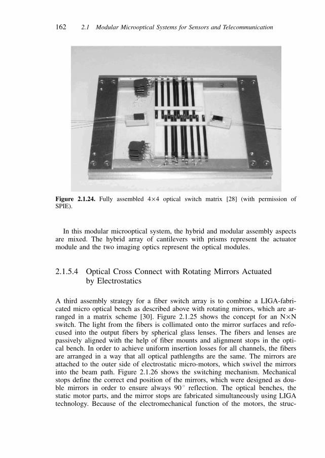
tive’ prism, one of the four output fibers is chosen. The light is coupled into theoutput fibers by means of another miniaturized focusing optics. Multiplying thissubsystem by a factor of four, the overall system is obtained. For assembly ofthe piezo actuators, a ceramic submount providing precise alignment grooveswas prepared. The prisms were assembled all in parallel using a vacuum matrixgripper [29] with triangular precision engineered grooves. The miniature focus-ing optics are shown in Figure 2.1.23. An Si fiber array with an angle polishededge is mounted on a ceramic base. In order to minimize back reflections, a cou-pling wedge is used to guide the light from the fibers to a micro-lens array. Thethree components are actively aligned and fixed with UV-curing glue. The fullsystem of a 4×4 switch array after electrical connection of the actuators andfiber insertion is shown in Figure 2.1.24.
A2.1.5 Opto-electromechanical Systems 2 161
Figure 2.1.22. Schematic drawing of hybrid fiber switch based on piezo actuators [28](with permission of SPIE).
Figure 2.1.23. Schematic drawing of miniaturized focusing optics [28] (with permissionof SPIE).
In this modular microoptical system, the hybrid and modular assembly aspectsare mixed. The hybrid array of cantilevers with prisms represent the actuatormodule and the two imaging optics represent the optical modules.
2.1.5.4 Optical Cross Connect with Rotating Mirrors Actuatedby Electrostatics
A third assembly strategy for a fiber switch array is to combine a LIGA-fabri-cated micro optical bench as described above with rotating mirrors, which are ar-ranged in a matrix scheme [30]. Figure 2.1.25 shows the concept for an N×Nswitch. The light from the fibers is collimated onto the mirror surfaces and refo-cused into the output fibers by spherical glass lenses. The fibers and lenses arepassively aligned with the help of fiber mounts and alignment stops in the opti-cal bench. In order to achieve uniform insertion losses for all channels, the fibersare arranged in a way that all optical pathlengths are the same. The mirrors areattached to the outer side of electrostatic micro-motors, which swivel the mirrorsinto the beam path. Figure 2.1.26 shows the switching mechanism. Mechanicalstops define the correct end position of the mirrors, which were designed as dou-ble mirrors in order to ensure always 90 � reflection. The optical benches, thestatic motor parts, and the mirror stops are fabricated simultaneously using LIGAtechnology. Because of the electromechanical function of the motors, the struc-
162 2.1 Modular Microoptical Systems for Sensors and Telecommunication
Figure 2.1.24. Fully assembled 4 ×4 optical switch matrix [28] (with permission ofSPIE).

A2.1.5 Opto-electromechanical Systems 2 163
Figure 2.1.25. Schematic drawing of N×N matrix switch using rotating mirrors.
Figure 2.1.26. Switching mechanism of rotating mirrors.

tures are made from electroplated nickel on a sacrificial layer [31]. The rotorswith the attached double mirrors are manufactured similarly on a separate sub-strate and are set manually above the stators. The fiber mounts from PMMA arepatterned on a third substrate. Figure 2.1.27 shows a close-up view of a fully as-sembled 2×2 switch matrix. On the left side, the fiber on the fiber mount and alens are pushed towards the stop structures of the optical bench. The mirror infront of the lens is in the ‘on’ position and the mirror below in the ‘off’ position.
This switch matrix can be considered as a fully hybrid set-up since all compo-nents and functions are finally placed on one substrate although they have beenfabricated on three substrates in total. It is a question of preference to define theoptical part with fibers and lenses as the optical module and the rotating mirroras the mechanical module.
2.1.5.5 Oscillating Modulator for Infrared Light Actuatedby Electromagnetics
To complete this section about opto-electro-mechanical systems including actua-tors, two examples from the sensor field are given. The first is a modulator, ie, achopper, for infrared light for suppression of noise in infrared spectrometers [32].The working principle becomes clear from the demonstrator shown in Figure2.1.28. Alignment structures for input and output fibers are patterned on a ceram-ic substrate in parallel with a movable shutter (looking like a small hammer inFigure 2.1.28) and an electromagnetic actuator, which becomes obvious from thecoil in the upper part of the picture. The structures are fabricated using LIGAtechnology and electroplating of Permalloy, which is a soft magnetic alloy of80% nickel and 20% iron. A current flowing through the coil generates a mag-netic field, which is guided through the metallic yoke. Owing to the decrease in
164 2.1 Modular Microoptical Systems for Sensors and Telecommunication
Figure 2.1.27. Close-up view of fully assembled 2 ×2 switch matrix.

the resistance of the magnetic circuit, the shutter is pulled backwards betweenthe pole shoes of the circuit, thus enhancing the metallic cross section for themagnetic field. A sinusoidal current generates a periodic field and an oscillationof the shutter. The yoke for the coil is manufactured on a separate substrate andreleased. The coil is wound manually so far and then assembled on the substrateusing alignment and clamping structures. For integration of the chopper in aspectrometer (discussed above in Section 2.1.4), the fiber alignment structuresare skipped. The chopper is put head-over in the light-input part of the spectrom-eter. This is facilitated by four stops on the edges of the yoke and the fixing
A2.1.5 Opto-electromechanical Systems 2 165
Figure 2.1.28. Demonstrator for electromagnetic microchopper.
Figure 2.1.29. Close-up of shutter in front of fiber.

block of the shutter, which were patterned simultaneously for this purpose. Fig-ure 2.1.29 shows a close-up view of the very precise position of the shutter tipdirectly in front of the input fiber of a spectrometer in its alignment groove.
The final system of the spectrometer including the chopper is a full modularassembly of an optical and an electromechanical module. The chopper itself is apure hybrid device.
2.1.5.6 Laser Scanner for Barcode Reading Actuatedby Electromagnetics
The second sensor example is a laser scanner for barcode reading [33] with asimilar actuation principle as the chopper. Figure 2.1.30 shows a schematic draw-ing of the scanner. Again, a magnetic circuit with an assembled coil is fabricatedfrom Permalloy by means of LIGA. A perpendicular mirror is attached on afreely suspended metal anchor, which is part of the magnetic circuit. The air gapin the circuit and therefore, the magnetic resistance are minimized when the an-
166 2.1 Modular Microoptical Systems for Sensors and Telecommunication
Figure 2.1.30. Schematic drawing of a laser scanner for barcode reading.
Figure 2.1.31. Stroboscopic photographs of a scanner at a deflection angle of 20 �.

chor is deflected towards the ends of the pole shoes. As above, a periodic currentwill generate an oscillation of the mirror with twice the current’s frequency. Themirror is made from a 100 �m thick Si wafer, which is coated with a reflectiveAu layer and cut to pieces of 1.5×1.6 mm2 by a wafer saw. It is placed in analignment groove, which was patterned in the anchor and is fixed by adhesivebonding. At a current of 20 mA, the scanner reaches a scan angle of 12 � in anonresonant mode. Figure 2.1.31 demonstrates the motion with two stroboscopicphotographs.
Like the chopper discussed before, the scanner is a hybrid device. In this case,however, it is a module in a ‘macroscopic’ optical system, which so far is notmade by means of micro-technology.
2.1.6 A Final Word About Assembly Technology
No matter what categories of opto-electro-mechanical systems were discussedabove, they all had one common task: assembly! Many components could be as-sembled passively using alignment aids such as stops or grooves, which were di-rectly patterned into the basic structures or substrates. If not, alignment had to bedone actively, which means that the performance of a device is optimized whileit is operated and the components are still under positioning control. For the fab-rication of demonstrators or prototypes, both assembly strategies are done moreor less manually. However, for industrial fabrication, automatic assembly proce-dures are desired. Several research groups are concerned with that target and aredeveloping grippers, bonders, dispensers for adhesives, and so on.
Some specific aspects for the assembly of microoptical devices are listed in[34]. The components have various but typical shapes such as spheres (balllenses), cylinders (mirrors, GRIN lenses, fibers), plates (mirrors, lens arrays) orprisms (beam splitters). They are small, of low weight and have smooth surfaces,which enhances adhesion. They are sensitive to electrostatic fields or mechanicalstress, the material typically is brittle so careful handling with the necessity ofsensing small gripping forces is required. Finally, the most important goal is notto damage the optical surfaces of the components that have to be picked andplaced. These handling conditions are also valid for all items concerned withstorage in magazines and transportation. Some examples given in [34] are a ma-gazine for cylinder lenses (Figure 2.1.32), a gripper for active alignment ofprisms (Figure 2.1.33) and a fiber gripper and manipulator (Figure 2.1.34). Themagazine allows safe storage of the cylinder lenses in a reproducible position. Itprovides a defined interface to the other assembly equipment with sufficientspace between the lenses to pick them up. The fiber manipulator consists of twogrippers, the first for stress relief and the second to pick the fiber at its uncoatedtip and for fine positioning, eg, when the fiber is threaded through a hole as indi-cated in Figure 2.1.34.
A2.1.6 A Final Word About Assembly Technology 167

A complete system for automatic assembly of a microoptical duplexer [35] forwhich ball lenses, monomode fibers, and wavelength filters have to be assembledinto an optical bench and a housing is described in [36]. The authors have devel-oped magazines and grippers for all components. All grippers work by vacuum suc-tion except the one for the fibers. For proper material flow during assembly, a com-plete tray on a xy-stage was developed which carries all magazines as sketched inFigure 2.1.35. The tray is pushed towards three reference pins to ensure a precise
168 2.1 Modular Microoptical Systems for Sensors and Telecommunication
Figure 2.1.32. Magazine for the storage of cylinder lenses [34] (with permission ofSPIE).
Figure 2.1.33. Gripper and alignment system for prisms [34] (with permission of SPIE).

position in the overall automatic assembly set-up. The magazines allow the storageof the pieceparts of six duplexer systems, which means that always one tray is in theassembly machine, and a second can be filled off-line with pieceparts in parallel.The diverse grippers and a dispenser for adhesive are mounted on a tool turret,which allows a fast change of tools while occupying only limited space becauseof its compact construction, as can be seen in Figure 2.1.36.
A2.1.6 A Final Word About Assembly Technology 169
Figure 2.1.34. Gripper and manipulator for fibers [34] (with permission of SPIE).
Figure 2.1.35. Work tray containing magazines for material flow during automatic assem-bly.

One very essential task for alignment and assembly is free sight to the devices nomatter whether microscopes are used for manual assembly or cameras for automaticprocesses. More complex positioning strategies are reported in [38] in the case offlip-chip assembly when the devices are mounted head-over and are hidden onebehind the other. As indicated in Figure 2.1.37, a laser chip is to be put on a fibersubmount. Both chips carry reference structures as alignment aids. One positioningstrategy is explained in Figure 2.1.38. The gripper for the laser chip is also equippedwith reference marks. When the chip is attached to the gripper, the relative positionof the chip to the gripper can be calculated from the image, which is detected by acamera below the chip. In the next step, the fiber submount is placed under a cam-era looking from above in order to calculate the relative position of the submountwith respect to the gripper. Finally, the flip-chip assembly is done automaticallyusing the calculated coordinates by an xy-stage. Another strategy makes use of aprism as an image splitter as shown in Figure 2.1.39. In this case, the camera isplaced beside the assembly, a prism is inserted in the free space between the twochips, and the reference marks of both chips are displayed in parallel. This set-up allows a closed-loop control of the alignment.
170 2.1 Modular Microoptical Systems for Sensors and Telecommunication
Figure 2.1.36. Tool turret carrying grippers and a dispenser.

A2.1.6 A Final Word About Assembly Technology 171
Figure 2.1.37. Flip-chip assembly of a laser chip on a fiber submount [37] (with permis-sion of SPIE).
Figure 2.1.38. Alignment strategy for flip-chip assembly using markers on the chip-grip-per [37] (with permission of SPIE).
Figure 2.1.39. Alignment strategy for flip-chip assembly using prisms as image splitter[37] (with permission of SPIE).

2.1.7 Conclusions
We have presented a wide variety of modular microoptical systems for telecom-munication and sensors. In doing so, we have distinguished between pure optomechanical devices and opto-electro-mechanical systems. Some of them repre-sent the modular aspect just very basically such as the fiber connectors (Section2.1.3) or the segmented mirror (Section 2.1.5.1). Other systems follow almostcompletely the modular method of design and manufacturing such as the dis-tance sensor (Section 2.1.4.3) or the fiber switch array (Section 2.1.5.2).
It is obvious from the wide range of concepts that we have described that themodular approach is convenient and helpful in order to produce more and morecomplex systems for always higher demands and broader applications. It allowsone to fabricate the separate modules with adapted processes, which are not toodifficult and time consuming and therefore not too expensive.
On the other hand, one has to ensure that these advantages are not overcomeby the costs and problems due to the consequently necessary assembly. Researchand development are performed for hybrid solutions, eg, magazines and assem-bly tools for single components such as lenses or fibers are investigated. How-ever, for a real modular approach to manufacturing and assembly, new strategiesneed to be found. Microfabricated components should not be first released fromtheir substrate, then be collected in a magazine which perhaps does not providesufficient position accuracy for a gripper to pick it up again without any need forimaging. In contrast, the method of assembly already needs to be considered inan ‘assembly friendly’ design of the diverse components and modules and intheir fabrication process.
The most important task, however, is the clear and unequivocal definition ofinterfaces. This is relevant for all aspects of hybrid and modular design andmanufacturing, not only for micro-optics but for all kind of systems. It includesinterfaces for on-going fabrication such as substrate size and chip size, compa-tible materials, how an intermediate product is supplied to the next fabricationstep, all assembly features including dicing, bonding, and packaging, and – final-ly and often forgotten – measurement methods with well-defined critical values.
The developers of modular micro-systems have to work hand in hand with thedevelopers of the assembly tools and also of the fabrication equipment. Themore they stick to the interfaces and standards, which mostly still need to be de-fined, the more they can use their developments for several modules or evenother purposes. This will make the modular approach economically feasible atleast for smaller and medium numbers of pieces such as are often required espe-cially in the sensor field.
172 2.1 Modular Microoptical Systems for Sensors and Telecommunication

2.1.8 References
[1] Deutsche Agenda, Optische Technologien für das 21. Jahrhundert, Düsseldorf: VDI-Technologiezentrum, 2000, pp. 3–6.
[2] Stix, G., Sci. Am. 284 (2001) 68–73.[3] Schramm, D., Engel, A., F&M-Feinwerktechnik 110, No. 3 (2002) 34–36.[4] Kiyoyuki, K., Kikins, R., Jolesz, F. A., in: Proc MICCAI99, Vol. 1679 (1999) 1020–
1031.[5] Product Overview, Fiber Optic Connectors, Europhotonics June/July (2000) 56–59.[6] Hibino, Y., Hanawa, F., Nakagome, H., Ishii, M., Takato, N., J. Lightwave Technol.
13 (1995) 1728–1735.[7] Bishop, D. J., Giles, C.R., Das, S.R., Sci. Am. 284 (2001) 74–79.[8] Sawada, R., Higurashi, E., Shimizu, A., Maruno, T., in: Proc. IEEE/LEOS Interna-
tional Conference on Optical MEMS 2001, Okinawa, 2001, pp. 23–24.[9] Marxer, C., de Rooij, N., J. Lightwave Technol. 17 (1999) 2–6.
[10] Field, L. A., Burriesci, D.L., Robrish, P.R., Ruby, R.C., Sens. Actuators A 53 (1996)311–315.
[11] Kim, Y., Neikirk, D.P., Sens. Actuators A 50 (1996) 141–146.[12] Debéda, H., v. Freyhold, T., Mohr, J., Wallrabe, U., Wengelink, J., J. Microelectro-
mech. Syst. 8 (1999) 258–263.[13] Mohr, J., Last, A., Hollenbach, U., Oka, T., Wallrabe, U., in: Proc. IEEE/LEOS
International Conference on Optical MEMS 2001, Okinawa, 2001, pp. 77–78.[14] Strandmann, C., Baecklund, Y., Proc. SPIE 2639 (1995) 18–24.[15] Hoffmann, M., Voges, E., Appl. Phys. B 73 (2001) 629–633.[16] Wallrabe, U., Dittrich, H., Friedsam, G., Hanemann, Th., Mohr, J., Müller, K., Piot-
ter, V., Ruther, P., Schaller, Th., Zissler, W., Microsyst. Technol. 8 (2002) 83–87.[17] Dunkel, K., Bauer, H.-D., Ehrfeld, W., Hossfeld, J., Weber, L., Hörcher, G., Müller,
G., J. Micromech. Microeng. 8 (1998) 301–306.[18] Schulze, J., Ehrfeld, W., Hossfeld, J., Klaus, M., Kufner, M., Kufner, S., Müller, H.,
Picard, A., Proc. SPIE 3737 (1999) 562–571.[19] Ziegler, P., Wengelink, J., Mohr, J., in: Proc. 3rd International Conference on Micro
Opto Electro Mechanical Systems MOEMS’99, Mainz, 1999, pp. 186–189.[20] Krippner, P., Kühner, T., Mohr, J., Saile, V., Proc. SPIE 3912 (2000) 141–149.[21] Hanemann, Th., Heckele, M., Piotter, V., Polym. News 25 (2000) 224–229.[22] Oka, T., Nakajima, H., Shiratsuki, A., Tsugai, M., Wallrabe, U., Hollenbach, U.,
Krippner, P., Mohr, J., in: Proc. 11th International Conference on Solid-State Sen-sors and Actuators, TRANSDUCER’01, Munich, 2001, pp. 536–539.
[23] Bonner, R., Nossal, R., Appl. Opt. 20 (1981) 2097–2107.[24] Higurashi, E., Sawada, R., Ito, T., in: Proc. IEEE/LEOS Optical MEMS 2002,
Lugano, IEEE Cat. No. 02EX610, 2002, pp. 33–34.[25] Peter, Y.-A., Carr, E., Solgaard, O., in: Proc. IEEE/LEOS Optical MEMS 2002,
Lugano, IEEE Cat. No. 02EX610, 2002, pp. 197–198.[26] Dellmann, L., Noell, W., Marxer, C., Weible, K., Hoffmann, M., de Rooij, N.F., in:
Proc. 11th International Conference on Solid-State Sensors and Actuators, TRANS-DUCER‘01, Munich, 2001, pp. 1332–1335.
[27] Noell, W., Clerc, P.-A., Dellmann, L., Guldimann, B., Herzig, H. P., Manzardo, O.,Marxer, C., Weible, K., Dändliker, R., de Rooij, N. F., IEEE J. Sel. Top. QuantumElectron. 8 (2002) 148–154.
A2.1.8 References 173
[28] Göhring, R., Wippermann, F., Kubitz, K., Proc. SPIE 4178 (2000) 59–66.[29] Göhring, R., Wippermann, F., Kubitz, K., Bücker, P., Götz, B., Proc. SPIE 3952
(2000) 339–345.[30] Ruzzu, A., Haller, D., Mohr, J., Wallrabe, U., Proc. SPIE 4178 (2000) 67–76.[31] Kunz, T., Kohl, M., Ruzzu, A., Skrobanek, K., Wallrabe, U., Microsyst. Technol. 6
(2000) 121–125.[32] Krippner, P., Mohr, J., Saile, V., Proc. SPIE 3878 (1999) 144.[33] Krevet, B., Hoffmann, S., Kohl, M., Mohr, J., Oliva, G., in: Proc. ACTUATOR 2002,
8th International Conference on New Actuators, Bremen, 2002, pp. 312–315.[34] Beckert, E., Mohaupt, M., Harnisch, G., Eberhardt, R., Proc. SPIE 4755 (2002)
531–548.[35] Müller, A., Göttert, J., Mohr, J., Rogner, A., Microsyst. Technol. 2 (1996) 40–45.[36] Gengenbach, U., Engelhardt, F., Scharnowell, R., in: Proc. Symposium on Handling
and Assembly of Microparts, Institute for Precision Engineering, Technical Univer-sity Vienna, Vienna, 1997, pp. 30–35.
[37] Reinhart, G., Jacob, D., Proc. SPIE 4178 (2000) 395–402.
List of Abbreviations
Abbreviation Explanation
DRIE deep reactive ion etchingLD laser diodeMEMS micro-electro-mechanical systemMOEMS micro-opto-electro-mechanical systemPD photodiodePMMA poly(methyl methacrylate)PSD position-sensitive detectorSEM scanning electron microscopeLIGA LIthography, Galvanik (electroplating),
Abformung (molding)
174 2.1 Modular Microoptical Systems for Sensors and Telecommunication


![of Hermitian Modular Forms. - uni-bielefeld.de · Definition 2.1. [24, page 31] A function f : H → C is called a Hermitian modular form for the congruence subgroup Γqof weight](https://static.fdocuments.in/doc/165x107/5eb79de051782c37106df872/of-hermitian-modular-forms-uni-definition-21-24-page-31-a-function-f-.jpg)