2048MB DDR3 – SDRAM SO-DIMM
14
Data Sheet Rev.1.0 08.05.2009 Swissbit Germany AG Wolfener Straße 36 Fon: +49 (0) 30 93 69 54 - 0 www.swissbit.com Page 1 D-12681 Berlin Fax: +49 (0) 30 93 69 54 - 55 eMail: [email protected] of 14 2048MB DDR3 – SDRAM SO-DIMM 204 Pin SO-DIMM SGN02G64B1BF2MT-CCR 2048MB PC3-10600 in FBGA Technique RoHS compliant Environmental Requirements: Operating temperature (ambient) Standard Grade 0°C to 70°C Grade W -40°C to 85°C Operating Humidity 10% to 90% relative humidity, noncondensing Operating Pressure 105 to 69 kPa (up to 10000 ft.) Storage Temperature -55°C to 100°C Storage Humidity 5% to 95% relative humidity, noncondensing Storage Pressure 1682 PSI (up to 5000 ft.) at 50°C Options: Frequency / Latency Marking DDR3 1333 MHz CL9 -CC DDR3 1066 MHz CL7 -BB Module densities 2048MB with 16 dies and 2 ranks Standard Grade (T A ) 0°C to 70°C (Tc) 0°C to 85°C Grade W (T A ) -40°C to 85°C (Tc) -40°C to 95°C Features: 204-pin 64-bit Small Outline, Dual-In-Line Double Data Rate synchronous DRAM Module DDR3 - SDRAM component base Micron MT41J128M8 V DD = 1.5V ±0.075V, V DDQ 1.5V ±0.075V Auto Refresh (CBR) and Self Refresh 8k Refresh every 64ms 1.5V I/O ( SSTL_15 compatible) Serial Presence Detect with EEPROM Four bit prefetch architecture DLL to align DQ and DQS transitions with CK Multiple internal device banks for concurrent operation Programmable CAS latency (CL) Posted CAS additive latency (AL) WRITE latency = READ latency – 1 t CK Programmable burst length: 8 or 4 Adjustable data-output drive strength On-die termination (ODT) Gold-contact pad This module family is fully pin and functional compatible to the JEDEC PC3-10600 spec. and JEDEC- Standard MO 224C. (see www.jedec.org ) The pcb and all components are manufactured according to the RoHS compliance specification [EU Directive 2002/95/EC Restriction of Hazardous Substances (RoHS)] Figure: mechanical dimensions
Transcript of 2048MB DDR3 – SDRAM SO-DIMM

Data Sheet Rev.1.0 08.05.2009
Swissbit Germany AG Wolfener Straße 36 Fon: +49 (0) 30 93 69 54 - 0 www.swissbit.com Page 1 D-12681 Berlin Fax: +49 (0) 30 93 69 54 - 55 eMail: [email protected] of 14
2048MB DDR3 – SDRAM SO-DIMM 204 Pin SO-DIMM
SGN02G64B1BF2MT-CCR
2048MB PC3-10600 in FBGA Technique
RoHS compliant
Environmental Requirements: � Operating temperature (ambient) Standard Grade 0°C to 70°C Grade W -40°C to 85°C � Operating Humidity 10% to 90% relative humidity, noncondensing � Operating Pressure 105 to 69 kPa (up to 10000 ft.) � Storage Temperature -55°C to 100°C � Storage Humidity 5% to 95% relative humidity, noncondensing � Storage Pressure 1682 PSI (up to 5000 ft.) at 50°C
Options: � Frequency / Latency Marking
DDR3 1333 MHz CL9 -CC DDR3 1066 MHz CL7 -BB
� Module densities 2048MB with 16 dies and 2 ranks
� Standard Grade (TA) 0°C to 70°C (Tc) 0°C to 85°C
� Grade W (TA) -40°C to 85°C (Tc) -40°C to 95°C
Features:
� 204-pin 64-bit Small Outline, Dual-In-Line Double Data Rate synchronous DRAM Module
� DDR3 - SDRAM component base Micron MT41J128M8
� VDD = 1.5V ±0.075V, VDDQ 1.5V ±0.075V � Auto Refresh (CBR) and Self Refresh 8k Refresh
every 64ms � 1.5V I/O ( SSTL_15 compatible) � Serial Presence Detect with EEPROM � Four bit prefetch architecture � DLL to align DQ and DQS transitions with CK � Multiple internal device banks for concurrent
operation � Programmable CAS latency (CL) � Posted CAS additive latency (AL) � WRITE latency = READ latency – 1 tCK � Programmable burst length: 8 or 4 � Adjustable data-output drive strength � On-die termination (ODT) � Gold-contact pad � This module family is fully pin and functional
compatible to the JEDEC PC3-10600 spec. and JEDEC- Standard MO 224C. (see www.jedec.org)
� The pcb and all components are manufactured according to the RoHS compliance specification [EU Directive 2002/95/EC Restriction of Hazardous Substances (RoHS)]
Figure: mechanical dimensions
Data Sheet Rev.1.0 08.05.2009
Swissbit Germany AG Wolfener Straße 36 Fon: +49 (0) 30 93 69 54 - 0 www.swissbit.com Page 2 D-12681 Berlin Fax: +49 (0) 30 93 69 54 - 55 eMail: [email protected] of 14
This Swissbit module is an industry standard 204-pin 8-byte DDR3 SDRAM Small Outline Dual-In-line Memory Module (SO-DIMM) which is organized as x64 high speed CMOS memory arrays. The module uses internally configured oct-bank DDR3 SDRAM devices. The module uses double data rate architecture to achieve high-speed operation. DDR3 SDRAM modules operate from a differential clock (CK and CK#). READ and WRITE accesses to a DDR3 SDRAM module is burst-oriented; accesses start at a selected location and continue for a programmed number of locations in a programmed sequence. The burst length is either four or eight locations. An auto precharge function can be enabled to provide a self-timed row precharge that is initiated at the end of a burst access. The DDR3 SDRAM devices have a multibank architecture which allows a concurrent operation that is providing a high effective bandwidth. A self refresh mode is provided and a power-saving “power-down” mode. All inputs and all full drive-strength outputs are SSTL_15 compatible. The DDR3 SDRAM module uses the serial presence detect (SPD) function implemented via serial EEPROM using the standard I2C protocol. This nonvolatile storage device contains 256 bytes. The first 128 bytes are utilized by the SO-DIMM manufacturer (Swissbit) to identify the module type, the module’s organization and several timing parameters. The second 128 bytes are available to the end user.
Module Configuration
Organization DDR3 SDRAMs used Row Addr. Device Bank
Select Col. Addr. Refresh Module Bank Select
256M x 64bit 16 x 128M x 8bit (1Gbit)
14 BA0, BA1, BA2
10 8k S0#, S1#
Module Dimensions
in mm
67.60 (long) x 30(high) x 4.10 [max] (thickness)
Timing Parameters
Part Number Module Density Transfer Rate Memory clock/Data bit rate Latency
SGN02G64B1BF2MT-BB[W]R 2048MB 8.5 GB/s 1.87ns/1066MT/s 8500-777
SGN02G64B1BF2MT-CC[W]R 2048MB 10.6 GB/s 1.5ns/1333MT/s 10600-999
Pin Name
A0-9, A11 – A13 Address Inputs
A10/AP Address Input / Autoprecharge Bit
BA0, BA1 Bank Address Inputs
DQ0 – DQ63 Data Input / Output
DM0-DM7 Input Data Mask
RAS# Row Address Strobe
CAS# Column Address Strobe
WE# Write Enable
CKE0 – CKE1 Clock Enable
CK0 – CK2 Clock Inputs, positive line
CK0# – CK2# Clock Inputs, negative line
DQS0 - DQS7 Data Strobe, positive line
DQS0# - DQS7# Data Strobe, negative line (only used when differential data strobe mode is enabled)
Data Sheet Rev.1.0 08.05.2009
Swissbit Germany AG Wolfener Straße 36 Fon: +49 (0) 30 93 69 54 - 0 www.swissbit.com Page 3 D-12681 Berlin Fax: +49 (0) 30 93 69 54 - 55 eMail: [email protected] of 14
S0#, S1# Chip Select
Event# Temperature event: The EVENT# pin is asserted by the temperature sensor when critical
VDD Supply Voltage (1.5V± 0.075V)
VREFDQ Reference voltage: DQ, DM (VDD/2)
VREFCA Reference voltage: Control, command, and address (VDD/2)
VSS Ground
VTT Termination voltage: Used for control, command, and address (VDD/2).
VDDSPD Serial EEPROM Positive Power Supply
SCL Serial Clock for Presence Detect
SDA Serial Data Out for Presence Detect
SA0 – SA1 Presence Detect Address Inputs
ODT0, ODT1 On-Die Termination
NC No Connection
Pin Configuration
Frontside
PIN Symbol PIN Symbol PIN Symbol PIN Symbol
1 VREFDQ 53 DQ19 105 VDD 155 VSS
3 VSS 55 VSS 107 A10 157 DQ42
5 DQ0 57 DQ24 109 BA0 159 DQ43
7 DQ1 59 DQ25 111 VDD 161 VSS
9 VSS 61 VSS 113 WE# 163 DQ48
11 DM0 63 DM3 115 CAS# 165 DQ49
13 VSS 65 VSS 117 VDD 167 VSS
15 DQ2 67 DQ26 119 A13 169 DQS6#
17 DQ3 69 DQ27 121 NC 171 DQS6
19 VSS 71 VSS 123 VDD 173 VSS
21 DQ8 73 CKE0 125 NC 175 DQ50
23 DQ9 75 VDD 127 VSS 177 DQ51
25 VSS 77 NC 129 DQ32 179 VSS
27 DQS1# 79 BA2 131 DQ33 181 DQ56
29 DQS1 81 VDD 133 VSS 183 DQ57
31 VSS 83 A12 135 DQS4# 185 VSS
33 DQ10 85 A9 137 DQS4 187 DM7
35 DQ11 87 VDD 139 VSS 189 VSS
37 VSS 89 A8 141 DQ34 191 DQ58
39 DQ16 91 A5 143 DQ35 193 DQ59
41 DQ17 93 VDD 145 VSS 195 VSS
43 VSS 95 A3 147 DQ40 197 SA0
45 DQS2# 97 A1 149 DQ41 199 VDDSPD
47 DQS2 99 VDD 151 VSS 201 SA1
49 VSS 101 CK0 153 DM5 203 VTT
51 DQ18 103 CK0#
Data Sheet Rev.1.0 08.05.2009
Swissbit Germany AG Wolfener Straße 36 Fon: +49 (0) 30 93 69 54 - 0 www.swissbit.com Page 4 D-12681 Berlin Fax: +49 (0) 30 93 69 54 - 55 eMail: [email protected] of 14
Backside
Pin Symbol Pin Symbol Pin Symbol Pin Symbol
2 VSS 54 VSS 106 VDD 156 VSS
4 DQ4 56 DQ28 108 BA1 158 DQ46
6 DQ5 58 DQ29 110 RAS# 160 DQ47
8 VSS 60 VSS 112 VDD 162 VSS
10 DQS0# 62 DQS3# 114 S0# 164 DQ52
12 DQS0 64 DQS3 116 ODT0 166 DQ53
14 VSS 66 VSS 118 VDD 168 VSS
16 DQ6 68 DQ30 120 NC 170 DM6
18 DQ7 70 DQ31 122 NC 172 VSS
20 VSS 72 VSS 124 VDD 174 DQ54
22 DQ12 74 NC 126 VREFCA 176 DQ55
24 DQ13 76 VDD 128 VSS 178 VSS
26 VSS 78 NC 130 DQ36 180 DQ60
28 DM1 80 NC/A14 132 DQ37 182 DQ61
30 Reset# 82 VDD 134 VSS 184 VSS
32 VSS 84 A11 136 DM4 186 DQS7#
34 DQ14 86 A7 138 VSS 188 DQS7
36 DQ15 88 VDD 140 DQ38 190 VSS
38 VSS 90 A6 142 DQ39 192 DQ62
40 DQ20 92 A4 144 VSS 194 DQ63
42 DQ21 94 VDD 146 DQ44 196 VSS
44 VSS 96 A2 148 DQ45 198 EVENT#
46 DM2 98 A0 150 VSS 200 SDA
48 VSS 100 VDD 152 DQS5# 202 SCL
50 DQ22 102 CK1 154 DQS5 204 VTT
52 DQ23 104 CK1#
Data Sheet Rev.1.0 08.05.2009
Swissbit Germany AG Wolfener Straße 36 Fon: +49 (0) 30 93 69 54 - 0 www.swissbit.com Page 5 D-12681 Berlin Fax: +49 (0) 30 93 69 54 - 55 eMail: [email protected] of 14
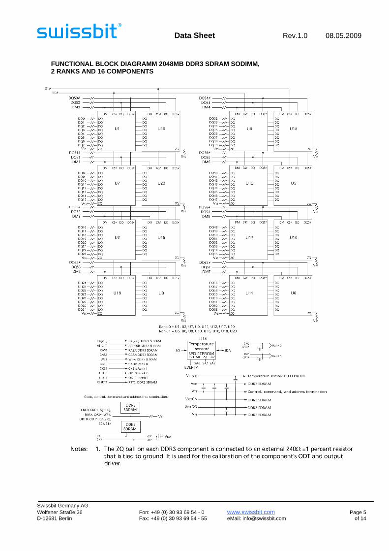
FUNCTIONAL BLOCK DIAGRAMM 2048MB DDR3 SDRAM SODIMM, 2 RANKS AND 16 COMPONENTS

Data Sheet Rev.1.0 08.05.2009
Swissbit Germany AG Wolfener Straße 36 Fon: +49 (0) 30 93 69 54 - 0 www.swissbit.com Page 6 D-12681 Berlin Fax: +49 (0) 30 93 69 54 - 55 eMail: [email protected] of 14
MAXIMUM ELECTRICAL DC CHARACTERISTICS
PARAMETER/ CONDITION SYMBOL MIN MAX UNITS Supply Voltage VDD -0.4 1.975 V I/O Supply Voltage VDDQ -0.4 1.975 V VDDL Supply Voltage VDDL -0.4 1.975 V Voltage on any pin relative to VSS Vin, Vout -0.4 1.975 V INPUT LEAKAGE CURRENT Any input 0V ≤ VIN ≤ VDD, VREF pin 0V ≤ VIN ≤ 0.95V (All other pins not under test = 0V)
Command/Address RAS#, CAS#, WE#, S#, CKE
-16 16
CK, CK# -16 16
DM
II
-2 2
µA
OUTPUT LEAKAGE CURRENT (DQ’s and ODT are disabled; 0V ≤ VOUT ≤ VDDQ) DQ, DQS, DQS#
IOZ -5 5 µA
VREF LEAKAGE CURRENT ; VREF is on a valid level IVREF -8 8 µA DC OPERATING CONDITIONS
PARAMETER/ CONDITION SYMBOL MIN NOM MAX UNITS Supply Voltage VDD 1.425 1.5 1.575 V I/O Supply Voltage VDDQ 1.425 1.5 1.575 V VDDL Supply Voltage VDDL 1.425 1.5 1.575 V I/O Reference Voltage VREF 0.49 x VDDQ 0.50 x VDDQ 0.51x VDDQ V I/O Termination Voltage (system) VTT 0.49 x VDDQ-20mV 0.50 x VDDQ 0.51x VDDQ+20mV V Input High (Logic 1) Voltage VIH (DC) VREF + 0.1 VDDQ + 0.3 V Input Low (Logic 0) Voltage VIL (DC) -0.3 VREF – 0.1 V AC INPUT OPERATING CONDITIONS
PARAMETER/ CONDITION SYMBOL MIN MAX UNITS Input High (Logic 1) Voltage VIH (AC) VREF + 0.175 - V Input Low (Logic 0) Voltage VIL (AC) - VREF - 0.175 V CAPACITANCE
At DDR3 data rates, it is recommended to simulate the performance of the module to achieve optimum values. When inductance and delay parameters associated with trace lengths are used in simulations, they are significantly more accurate and realistic than a gross estimation of module capacitance. Simulations can then render a considerably more accurate result. JEDEC modules are now designed by using simulations to close timing budgets.
Data Sheet Rev.1.0 08.05.2009
Swissbit Germany AG Wolfener Straße 36 Fon: +49 (0) 30 93 69 54 - 0 www.swissbit.com Page 7 D-12681 Berlin Fax: +49 (0) 30 93 69 54 - 55 eMail: [email protected] of 14
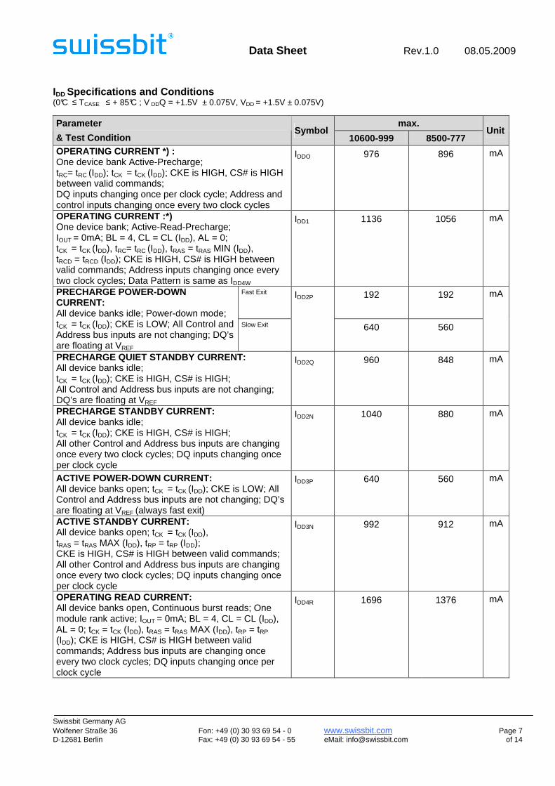
IDD Specifications and Conditions (0°C ≤ TCASE ≤ + 85°C ; V DDQ = +1.5V ± 0.075V, VDD = +1.5V ± 0.075V)
max. Parameter
& Test Condition Symbol
10600-999 8500-777 Unit
OPERATING CURRENT *) : One device bank Active-Precharge; tRC= tRC (IDD); tCK = tCK (IDD); CKE is HIGH, CS# is HIGH between valid commands; DQ inputs changing once per clock cycle; Address and control inputs changing once every two clock cycles
IDDO 976 896 mA
OPERATING CURRENT :*) One device bank; Active-Read-Precharge; IOUT = 0mA; BL = 4, CL = CL (IDD), AL = 0; tCK = tCK (IDD), tRC= tRC (IDD), tRAS = tRAS MIN (IDD), tRCD = tRCD (IDD); CKE is HIGH, CS# is HIGH between valid commands; Address inputs changing once every two clock cycles; Data Pattern is same as IDD4W
IDD1 1136 1056 mA
Fast Exit
192 192 PRECHARGE POWER-DOWN CURRENT: All device banks idle; Power-down mode; tCK = tCK (IDD); CKE is LOW; All Control and Address bus inputs are not changing; DQ’s are floating at VREF
Slow Exit
IDD2P
640 560
mA
PRECHARGE QUIET STANDBY CURRENT: All device banks idle; tCK = tCK (IDD); CKE is HIGH, CS# is HIGH; All Control and Address bus inputs are not changing; DQ’s are floating at VREF
IDD2Q 960 848 mA
PRECHARGE STANDBY CURRENT: All device banks idle; tCK = tCK (IDD); CKE is HIGH, CS# is HIGH; All other Control and Address bus inputs are changing once every two clock cycles; DQ inputs changing once per clock cycle
IDD2N 1040 880 mA
ACTIVE POWER-DOWN CURRENT: All device banks open; tCK = tCK (IDD); CKE is LOW; All Control and Address bus inputs are not changing; DQ’s are floating at VREF (always fast exit)
IDD3P 640 560 mA
ACTIVE STANDBY CURRENT: All device banks open; tCK = tCK (IDD), tRAS = tRAS MAX (IDD), tRP = tRP (IDD); CKE is HIGH, CS# is HIGH between valid commands; All other Control and Address bus inputs are changing once every two clock cycles; DQ inputs changing once per clock cycle
IDD3N 992 912 mA
OPERATING READ CURRENT: All device banks open, Continuous burst reads; One module rank active; IOUT = 0mA; BL = 4, CL = CL (IDD), AL = 0; tCK = tCK (IDD), tRAS = tRAS MAX (IDD), tRP = tRP (IDD); CKE is HIGH, CS# is HIGH between valid commands; Address bus inputs are changing once every two clock cycles; DQ inputs changing once per clock cycle
IDD4R 1696 1376 mA

Data Sheet Rev.1.0 08.05.2009
Swissbit Germany AG Wolfener Straße 36 Fon: +49 (0) 30 93 69 54 - 0 www.swissbit.com Page 8 D-12681 Berlin Fax: +49 (0) 30 93 69 54 - 55 eMail: [email protected] of 14
max. Parameter
& Test Condition Symbol
10600-999 8500-777 Unit
OPERATING WRITE CURRENT: All device banks open, Continuous burst writes; One module rank active; BL = 4, CL = CL (IDD), AL = 0; tCK = tCK (IDD), tRAS = tRAS MAX (IDD), tRP = tRP (IDD); CKE is HIGH, CS# is HIGH between valid commands; Address bus inputs are changing once every two clock cycles; DQ inputs changing once per clock cycle
IDD4W 1856 1616 mA
BURST REFRESH CURRENT: tCK = tCK (IDD); refresh command at every tRFC (IDD) interval, CKE is HIGH, CS# is HIGH between valid commands; All other Control and Address bus inputs are changing once every two clock cycles; DQ inputs changing once per clock cycle
IDD5 3840 3520 mA
SELF REFRESH CURRENT: CK and CK# at 0V; CKE ≤ 0.2V; All other Control and Address bus inputs are floating at VREF; DQ’s are floating at VREF
IDD6 96 96 mA
OPERATING CURRENT*) : Four device bank interleaving READs, IOUT = 0mA; BL = 4, CL = CL (IDD), AL = tRCD (IDD) – 1 x tCK (IDD); tCK = tCK (IDD), tRC = tRC (IDD), tRRD = tRRD (IDD), tRCD = tRCD (IDD); CKE is HIGH, CS# is HIGH between valid commands; Address bus inputs are not changing during DESELECT; DQ inputs changing once per clock cycle
IDD7 4016 3216 mA
*) Value calculated as one module rank in this oper ating condition, and all other module ranks in IDD2 P (CKE LOW) mode. TIMING VALUES USED FOR IDD MEASUREMENT
IDD MEASUREMENT CONDITIONS SYMBOL 10600-999 8500-777 Unit CL (IDD) 9 7 tCK tRCD (IDD) 13.5 13.125 ns tRC (IDD) 49.5 50.625 ns tRRD (IDD) 6 7.5 ns tCK (IDD) 1.5 1,87 ns tRAS MIN (IDD) 36 37.5 ns tRAS MAX (IDD) 70,200 70,200 ns tRP (IDD) 13.5 13.125 ns tRFC (IDD) 110 110 ns
Data Sheet Rev.1.0 08.05.2009
Swissbit Germany AG Wolfener Straße 36 Fon: +49 (0) 30 93 69 54 - 0 www.swissbit.com Page 9 D-12681 Berlin Fax: +49 (0) 30 93 69 54 - 55 eMail: [email protected] of 14
DDR3 SDRAM COMPONENT ELECTRICAL CHARACTERISTICS AND RECO MMENDED AC OPERATING CONDITIONS (0°C ≤ TCASE ≤ + 85°C; V DDQ = +1.5V ± 0.075V, VDD = +1.5V ± 0.075V)
AC CHARACTERISTICS 10600-999 8500-777 PARAMETER SYMBOL MIN MAX Min MAX Unit Clock cycle time CL = 10 tCK (10) 1.5 <1.875 - - ns
CL = 9 tCK (9) 1.5 <1.875 - - ns CL = 8 tCK (8) 1.875 <2.5 - - ns CL = 7 tCK (7) 1.875 <2.5 1.875 <2.5 ns
CL = 6 tCK (6) 2.5 3.3 2.5 3.3 ns CK high-level width tCH 0.47 0.53 0.47 0.53 tCK CK low-level width tCL 0.47 0.53 0.47 0.53 tCK Data-out high-impedance window from CK/CK#
tHZ 0.25 0.3 ns
Data-out low-impedance window from CK/CK#
tLZ -0.5 0.25 -0.6 0.3 ns
DQ and DM input setup time relative to DQS
tDS(Base) 30 25 ps
DQ and DM input hold time relative to DQS
tDH(Base) 65 100 ps
DQ and DM input setup time relative to DQS VREF=1V/ns
tDS1V 180 200 ps
DQ and DM input hold time relative to DQS VREF=1V/ns
tDH1V 165 200 ps
DQ and DM input pulse width ( for each input )
tDIPW 0.4 0.49 ns
DQS, DQS# to DQ skew, per access
tDQSQ 125 150 ps
DQ-DQS hold, DQS to first DQ to go non-valid, per access
tQH 0.38
0.38 tCK
(AVG) DQS input high pulse width tDQSH 0.45 0.55 0.45 0.55 tCK DQS input low pulse width tDQSL 0.45 0.55 0.45 0.55 tCK DQS, DQS# rising to/from CK, CK#
tDQSCK -255 +255 -300 300 ps
DQS, DQS# rising to/from CK, CK# when DLL disabled
tDQSCK
DLL_DIS 1 10 1 10 ns
DQS falling edge to CK rising - setup time
tDSS 0.2 0.2 tCK
DQS falling edge from CK rising - hold time
tDSH 0.2 0.2 tCK
DQS read preamble tRPRE 0.9 Note1 0.9 Note1 tCK DQS read postamble tRPST 0.3 Note2 0.3 Note2 tCK DQS write preamble tWPRE 0.9 0.9 tCK DQS write postamble tWPST 0.3 0.3 tCK Positive DQS latching edge to associated clock edge
tDQSS - 0.25 + 0.25 - 0.25 + 0.25 tCK
Address and control input pulse width ( for each input )
tIPW 400 490 ps
CTRL, CMD, Addr setup to CK, CK#
tIS(Base) 65 125 ps
CTRL, CMD, Addr setup to CK, CK# VREF @ 1V/ns
tIS(1V) 240 300 ps
1 The maximum preamble is bound by tLZDQS (MAX) 2 The maximum postamble is bound by tHZDQS (MAX)

Data Sheet Rev.1.0 08.05.2009
Swissbit Germany AG Wolfener Straße 36 Fon: +49 (0) 30 93 69 54 - 0 www.swissbit.com Page 10 D-12681 Berlin Fax: +49 (0) 30 93 69 54 - 55 eMail: [email protected] of 14
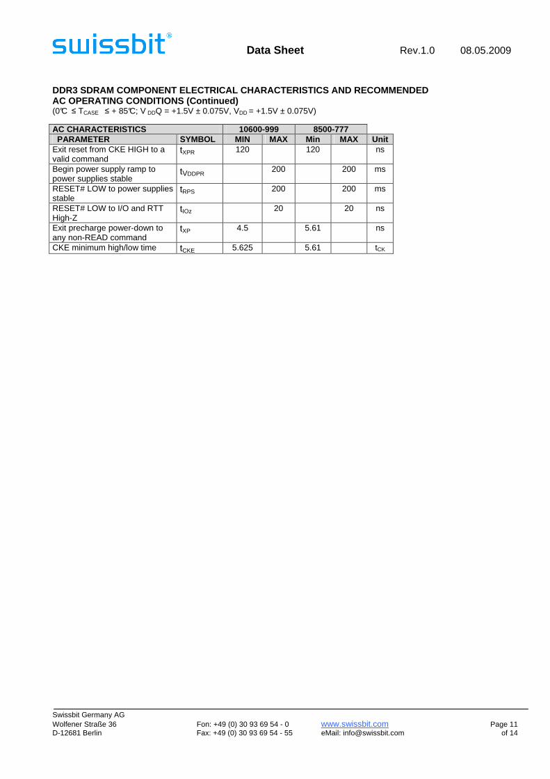
DDR3 SDRAM COMPONENT ELECTRICAL CHARACTERISTICS AND RECO MMENDED AC OPERATING CONDITIONS (Continued) (0°C ≤ TCASE ≤ + 85°C; V DDQ = +1.5V ± 0.075V, VDD = +1.5V ± 0.075V)
AC CHARACTERISTICS 10600-999 8500-777 PARAMETER SYMBOL MIN MAX MIN MAX Unit CTRL, CMD, Addr hold to CK, CK# tIH(Base) 140 200 ps
CTRL, CMD, Addr hold to CK, CK# VREF @ 1V/ns tIH(1V) 240 300 ps
CAS# to CAS# command delay tCCD 4 4 tCK
ACTIVE to ACTIVE (same bank) command period tRC 49.5 50.625 ns
ACTIVE bank a to ACTIVE bank b command tRRD 6 7.5 ns
ACTIVE to READ or WRITE delay tRCD 13.5 13.125 ns
1K Page size 30 37.5 Four bank Activate period 2K Page size
tFAW 45 50
ns
ACTIVE to PRECHARGE command tRAS 36 70,200 37.5 70,200 ns
Internal READ to precharge command delay tRTP 7.5 7.5 ns
Write recovery time tWR 15 15 ns Auto precharge write recovery + precharge time tDAL tWR + tRP/tCK tWR +
tRP/tCK ns
Internal WRITE to READ command delay tWTR 7.5 7.5 ns
PRECHARGE command period tRP 15 13.125 ns LOAD MODE command cycle time tMRD 6 7.5 tCK
REFRESH to ACTIVE or REFRESH to REFRESH command interval
tRFC 110 70,200 110 70,200 ns
Average periodic refresh interval tREFI 7.8 7.8 µs RTT turn-on from ODTL on reference tAON -250 250 -300 300 ps
RTT turn-on from ODTL off reference tAOF 0.3 0.7 0.3 0.7 tCK
Asynchronous RTT turn-on delay (power Down with DLL off) tAONPD 1 9 1 9 ns
Asynchronous RTT turn-off delay (power Down with DLL off) tAOFPD 1 9 1 9 ns
RTT dynamic change skew tADC 0.3 0.7 0.3 0.7 tCK Exit self refresh to commands not requiring a locked DLL tXS 120 120 ns
Write levelling setup from rising CK, CK# crossing to rising DQS, DQS# crossing
tWLS 195 245 ps
Write levelling setup from rising DQS, DQS# crossing to rising CK, CK# crossing
tWLH 195 245 ps
First DQS, DQS# rising edge tWLMRD 40 40 tCK
DQS, DQS# delay tWLDQSEN 25 25 tCK
Data Sheet Rev.1.0 08.05.2009
Swissbit Germany AG Wolfener Straße 36 Fon: +49 (0) 30 93 69 54 - 0 www.swissbit.com Page 11 D-12681 Berlin Fax: +49 (0) 30 93 69 54 - 55 eMail: [email protected] of 14
DDR3 SDRAM COMPONENT ELECTRICAL CHARACTERISTICS AND RECO MMENDED AC OPERATING CONDITIONS (Continued) (0°C ≤ TCASE ≤ + 85°C; V DDQ = +1.5V ± 0.075V, VDD = +1.5V ± 0.075V)
AC CHARACTERISTICS 10600-999 8500-777 PARAMETER SYMBOL MIN MAX Min MAX Unit Exit reset from CKE HIGH to a valid command
tXPR 120 120 ns
Begin power supply ramp to power supplies stable
tVDDPR 200 200 ms
RESET# LOW to power supplies stable
tRPS 200 200 ms
RESET# LOW to I/O and RTT High-Z
tIOz 20 20 ns
Exit precharge power-down to any non-READ command
tXP 4.5 5.61 ns
CKE minimum high/low time tCKE 5.625 5.61 tCK
Data Sheet Rev.1.0 08.05.2009
Swissbit Germany AG Wolfener Straße 36 Fon: +49 (0) 30 93 69 54 - 0 www.swissbit.com Page 12 D-12681 Berlin Fax: +49 (0) 30 93 69 54 - 55 eMail: [email protected] of 14
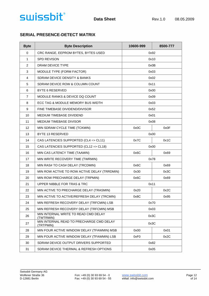
SERIAL PRESENCE-DETECT MATRIX
Byte Byte Description 10600-999 8500-777
0 CRC RANGE, EEPROM BYTES, BYTES USED 0x92
1 SPD REVISON 0x10
2 DRAM DEVICE TYPE 0x0B
3 MODULE TYPE (FORM FACTOR) 0x03
4 SDRAM DEVICE DENSITY & BANKS 0x02
5 SDRAM DEVICE ROW & COLUMN COUNT 0x11
6 BYTE 6 RESERVED 0x00
7 MODULE RANKS & DEVICE DQ COUNT 0x09
8 ECC TAG & MODULE MEMORY BUS WIDTH 0x03
9 FINE TIMEBASE DIVIDEND/DIVISOR 0x52
10 MEDIUM TIMEBASE DIVIDEND 0x01
11 MEDIUM TIMEBASE DIVISOR 0x08
12 MIN SDRAM CYCLE TIME (TCKMIN) 0x0C 0x0F
13 BYTE 13 RESERVED 0x00
14 CAS LATENCIES SUPPORTED (CL4 => CL11) 0x7C 0x1C
15 CAS LATENCIES SUPPORTED (CL12 => CL18) 0x00
16 MIN CAS LATENCY TIME (TAAMIN) 0x6C 0x69
17 MIN WRITE RECOVERY TIME (TWRMIN) 0x78
18 MIN RAS# TO CAS# DELAY (TRCDMIN) 0x6C 0x69
19 MIN ROW ACTIVE TO ROW ACTIVE DELAY (TRRDMIN) 0x30 0x3C
20 MIN ROW PRECHARGE DELAY (TRPMIN) 0x6C 0x69
21 UPPER NIBBLE FOR TRAS & TRC 0x11
22 MIN ACTIVE TO PRECHARGE DELAY (TRASMIN) 0x20 0x2C
23 MIN ACTIVE TO ACTIVE/REFRESH DELAY (TRCMIN) 0x8C 0x95
24 MIN REFRESH RECOVERY DELAY (TRFCMIN) LSB 0x70
25 MIN REFRESH RECOVERY DELAY (TRFCMIN) MSB 0x03
26 MIN INTERNAL WRITE TO READ CMD DELAY (TWTRMIN) 0x3C
27 MIN INTERNAL READ TO PRECHARGE CMD DELAY (TRTPMIN)
0x3C
28 MIN FOUR ACTIVE WINDOW DELAY (TFAWMIN) MSB 0x00 0x01
29 MIN FOUR ACTIVE WINDOW DELAY (TFAWMIN) LSB 0xF0 0x2C
30 SDRAM DEVICE OUTPUT DRIVERS SUPPORTED 0x82
31 SDRAM DEVICE THERMAL & REFRESH OPTIONS 0x05
Data Sheet Rev.1.0 08.05.2009
Swissbit Germany AG Wolfener Straße 36 Fon: +49 (0) 30 93 69 54 - 0 www.swissbit.com Page 13 D-12681 Berlin Fax: +49 (0) 30 93 69 54 - 55 eMail: [email protected] of 14
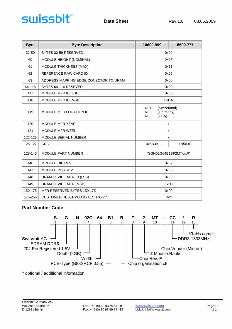
Byte Byte Description 10600-999 8500-777
32-59 BYTES 32-59 RESERVED 0x00
60 MODULE HEIGHT (NOMINAL) 0x0F
61 MODULE THICKNESS (MAX) 0x11
62 REFERENCE RAW CARD ID 0x05
63 ADDRESS MAPPING EDGE CONECTOR TO DRAM 0x00
64-116 BYTES 64-116 RESEVED 0x00
117 MODULE MFR ID (LSB) 0x83
118 MODULE MFR ID (MSB) 0xDA
119 MODULE MFR LOCATION ID 0x01 (Swizerland) 0x02 (Germany) 0x03 (USA)
120 MODULE MFR YEAR x
121 MODULE MFR WEEK x
122-125 MODULE SERIAL NUMBER x
126-127 CRC 0x5B3A 0x503F
128-145 MODULE PART NUMBER "SGN02G64B1BF2MT-xxR"
146 MODULE DIE REV 0x52
147 MODULE PCB REV 0x00
148 DRAM DEVICE MFR ID (LSB) 0x80
149 DRAM DEVICE MFR (MSB) 0x2C
150-175 MFR RESERVED BYTES 150-175 0x00
176-255 CUSTOMER RESERVED BYTES 176-255 0xff
Part Number Code
S G N 02G 64 B1 B F 2 MT - CC * R 1 2 3 4 5 6 7 8 9 10 11 12 13
*RoHs compl. Swissbit AG DDR3-1333MHz
SDRAM DDR3 204 Pin Registered 1.5V Chip Vendor (Micron)
Depth (2GB) 2 Module Ranks Width Chip Rev. F
PCB-Type (B83SRCF 0.55) Chip organisation x8
* optional / additional information

Data Sheet Rev.1.0 08.05.2009
Swissbit Germany AG Wolfener Straße 36 Fon: +49 (0) 30 93 69 54 - 0 www.swissbit.com Page 14 D-12681 Berlin Fax: +49 (0) 30 93 69 54 - 55 eMail: [email protected] of 14
Locations
Swissbit AG Industriestrasse 4 – 8 CH – 9552 Bronschhofen Switzerland Phone: +41 (0)71 913 72 66 Fax: +41 (0)71 913 74 50 new phone numbers effective from 28.01.2009 Phone: +41 (0)71 913 03 03 Fax: +41 (0)71 913 03 15 _____________________________ Swissbit Germany GmbH Wolfener Strasse 36 D – 12681 Berlin Germany Phone: +49 (0)30 93 69 54 – 0 Fax: +49 (0)30 93 69 54 – 55 _____________________________ Swissbit NA, Inc. 14 Willett Avenue, Suite 301A Port Chester, NY 10573 USA Phone: +1 914 935 1400 Fax: +1 914 935 9865 _____________________________ Swissbit NA, Inc. 3913 Todd Lane, Suite – 307 Austin, TX 78744 USA Phone: +1 512 302 9001 Fax: +1 512 302 4808 _____________________________ Swissbit Japan, Inc. 3F Core Koenji, 2-1-24 Koenji-Kita, Suginami-Ku, Tokyo 166-0002 Japan Phone: +81 3 5356 3511 Fax: +81 3 5356 3512