2018 Product overview - Vectrawave · integrated circuits (MMIC), solutions using SiP (system in a...
32
2018 Product overview
Transcript of 2018 Product overview - Vectrawave · integrated circuits (MMIC), solutions using SiP (system in a...

2018Product overview
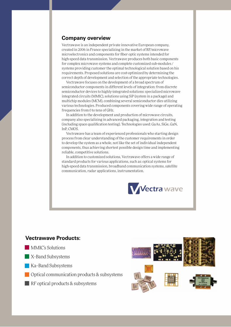
Vectrawave is an independent private innovative European company, created in 2006 in France specializing in the market of RF/microwave microelectronics and components for fiber optic systems intended for high-speed data transmission. Vectrawave produces both basic components for complex microwave systems and complete customized sub-modules / systems providing customer the optimal technological solution based on his requirements. Proposed solutions are cost-optimized by determining the correct depth of development and selection of the appropriate technologies.
Vectrawave focuses on the development of a broad spectrum of semiconductor components in different levels of integration: from discrete semiconductor devices to highly-integrated solutions: specialized microwave integrated circuits (MMIC), solutions using SiP (system in a package) and multichip modules (MCM), combining several semiconductor dies utilizing various technologies. Produced components covering wide range of operating frequencies from 0 to tens of GHz.
In addition to the development and production of microwave circuits, company also specializing in advanced packaging, integration and testing (including space qualification testing). Technologies used: GaAs, SiGe, GaN, InP, CMOS.
Vectrawave has a team of experienced professionals who starting design process from clear understanding of the customer requirements in order to develop the system as a whole, not like the set of individual independent components, thus achieving shortest possible design time and implementing reliable, competitive solutions.
In addition to customized solutions, Vectrawave offers a wide range of standard products for various applications, such as: optical systems for high-speed data transmission, broadband communication systems, satellite communication, radar applications, instrumentation.
MMIC’s Solutions
X–Band Subsystems
Ka–Band Subsystems
Optical communication products & subsystems
RF optical products & subsystems
Company overview
Vectrawave Products:
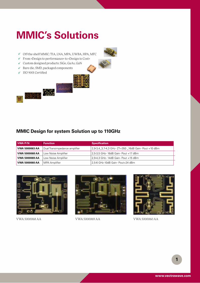
MMIC’s Solutions
MMIC Design for system Solution up to 110GHz
www.vectrawave.com
Off-the-shelf MMIC: TIA, LNA, MPA, UWBA, HPA, MFCFrom «Design to performance» to «Design to Cost»Custom designed products: SiGe, GaAs, GaN
Bare die, SMD, packaged componentsISO 9001 Certified
VWA P/N Function Specification
VWA 5000063 AA Dual Transimpedance amplifier 2,9-3,4_3,7-4,3 GHz - ZT=350 _16dB Gain - Pout +10 dBm
VWA 5000068 AA Low Noise Amplifier 2,5-3,5 GHz - 16dB Gain - Pout +17 dBm
VWA 5000069 AA Low Noise Amplifier 2,9-4,3 GHz - 14dB Gain - Pout +15 dBm
VWA 5000060 AA MPA Amplifier 2,5-6 GHz -10dB Gain - Pout+24 dBm
VWA 5000068 AA VWA 5000069 AA VWA 5000060 AA
1

GaAs HPA = 5W, 9W,10W, 12W, 15WGaN/SiC HPA = 35W
VWA 5000057 AA = DPS 6 Bits /7-13 GHzVWA 5000055 AA = DAT 5 Bits /DC – 18GHzVWA 5000049 AA = MFC /8-12 GHzVWA 5005017 LA = LNA /8-12 GHz
Chip Set 1: LNA, MFC, HPA (MPA)Chip Set 2: LNA, DPS, DAT, MPA, HPA
TX/RX MMIC chipset solution
X Band Design Kit for T/R Die Status
P/N Function Frequency Gain/A/PHI Size (mm) P,E
VWA 5000061 AA Gain Block Amplifier 7 to 13 GHz 13dB 2,3X3,0X0,1 P
VWA 50035 AA Medium Power Amplifier 8 to 13 GHz 22dB 3,5X2,9X0,2 P
VWA 50035 AC Medium Power Amplifier 8 to 12 GHz 22dB 2,3X1,8X0,1 P
VWA 5000058 AA High Power Amplifier (2 Stages) 8 to 11GHz 21dB 1,4X4,4X0,1 P
VWA 5000059 AA High Power Amplifier (2 Stages) 9 to 11GHz 21dB 2,5X4,4X0,1 P
VWA 50036 AC High Power Amplifier (3 Stages) 7 to 13 GHz 21dB 4,1X4,4X0,1 P
VWA 5000070 AA High Power Amplifier (2 Stages) 8.5 to 10.5GHz 17dB 4,4X3,6X0,1 P
VWA 5000042 AA High Power Amplifier (3 Stages) 8 to 12 GHz 25dB 3,9X4,5X0,1 P
VWA 5005017 LA Low Noise Amplifier (NF=1,6dB) 9 to 12 GHz 19dB 1,6X1,1X0,1 P
VWA 5000048 AA Low Noise Amplifier (NF=1,1dB) 8 to 12 GHz 32dB 2,4X1,56X0,1 P
VWA 5000055 AA 5 Bits Digital Attenuator DC-18GHz 31dB/5 Bits 2,4X1,55X0,1 P
VWA 5000057 AA 6 Bits Digital Phase Shifter 7-13 GHz 360°/6 Bits 3X2,1X0,1 P
VWA 5000049 AA Multi Function Chip (DPS/DAT) 8 to 12 GHz 20dB 4X5X0,1 P
Усилитель мощностиVWA 5000042 AA
Функциональная блок-диаграмма
VWA 5000048 AA
VWA 5000049 AA МШУ
LNA
Антенна
A.
HPA
Con
trol
In
terf
ace
Tx
Rx
DF
Tx/Rx
Многофункциональная микросхема (Core Chip)
Power AmplifierVWA 5000042 AA/VWA 5000059 AA
MFCVWA 5000049 AA
LNAVWA 5000048 AA, /VWA 5005017 LA
Antenna
2
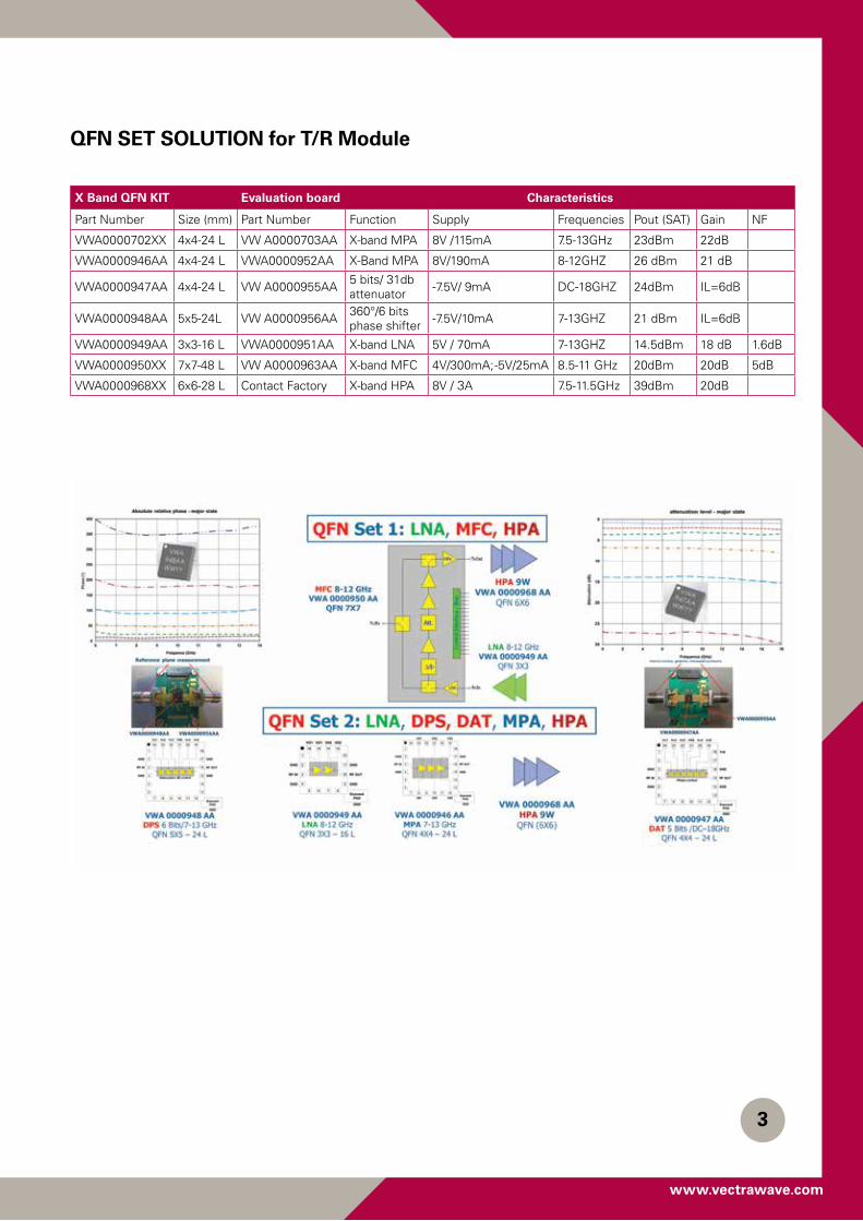
QFN SET SOLUTION for T/R Module
www.vectrawave.com
X Band QFN KIT Evaluation board Characteristics
Part Number Size (mm) Part Number Function Supply Frequencies Pout (SAT) Gain NF
VWA0000702XX 4x4-24 L VW A0000703AA X-band MPA 8V /115mA 7.5-13GHz 23dBm 22dB
VWA0000946AA 4x4-24 L VWA0000952AA X-Band MPA 8V/190mA 8-12GHZ 26 dBm 21 dB
VWA0000947AA 4x4-24 L VW A0000955AA 5 bits/ 31db attenuator -7.5V/ 9mA DC-18GHZ 24dBm IL=6dB
VWA0000948AA 5x5-24L VW A0000956AA 360°/6 bits phase shifter -7.5V/10mA 7-13GHZ 21 dBm IL=6dB
VWA0000949AA 3x3-16 L VWA0000951AA X-band LNA 5V / 70mA 7-13GHZ 14.5dBm 18 dB 1.6dB
VWA0000950XX 7x7-48 L VW A0000963AA X-band MFC 4V/300mA; -5V/25mA 8.5-11 GHz 20dBm 20dB 5dB
VWA0000968XX 6x6-28 L Contact Factory X-band HPA 8V / ЗА 7.5-11.5GHz 39dBm 20dB
3
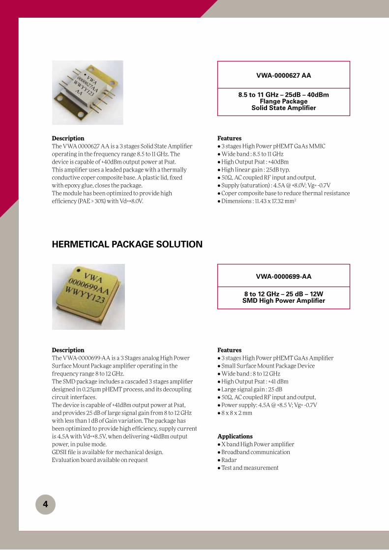
HERMETICAL PACKAGE SOLUTION
VWA-0000627 AA
8.5 to 11 GHz – 25dB – 40dBmFlange Package
Solid State Amplifier
VWA-0000699-AA
8 to 12 GHz – 25 dB – 12WSMD High Power Amplifier
DescriptionThe VWA 0000627 AA is a 3 stages Solid State Amplifieroperating in the frequency range 8.5 to 11 GHz. Thedevice is capable of +40dBm output power at Psat.This amplifier uses a leaded package with a thermallyconductive coper composite base. A plastic lid, fixedwith epoxy glue, closes the package.The module has been optimized to provide highefficiency (PAE > 30%) with Vd=+8.0V.
DescriptionThe VWA-0000699-AA is a 3 Stages analog High Power Surface Mount Package amplifier operating in the frequency range 8 to 12 GHz.The SMD package includes a cascaded 3 stages amplifier designed in 0.25μm pHEMT process, and its decoupling circuit interfaces.The device is capable of +41dBm output power at Psat, and provides 25 dB of large signal gain from 8 to 12 GHz with less than 1 dB of Gain variation. The package has been optimized to provide high efficiency, supply current is 4.5A with Vd=+8.5V, when delivering +41dBm output power, in pulse mode.GDSII file is available for mechanical design.Evaluation board available on request
Features• 3 stages High Power pHEMT GaAs MMIC• Wide band : 8.5 to 11 GHz• High Output Psat : +40dBm• High linear gain : 25dB typ.• 50Ω, AC coupled RF input and output,• Supply (saturation) : 4.5A @ +8.0V; Vg= -0.7V• Coper composite base to reduce thermal resistance• Dimensions : 11.43 x 17.32 mm2
Features• 3 stages High Power pHEMT GaAs Amplifier• Small Surface Mount Package Device• Wide band : 8 to 12 GHz• High Output Psat : +41 dBm• Large signal gain : 25 dB• 50Ω, AC coupled RF input and output,• Power supply: 4.5A @ +8.5 V; Vg= -0.7V• 8 x 8 x 2 mm
Applications• X band High Power amplifier• Broadband communication• Radar• Test and measurement
4
www.vectrawave.com
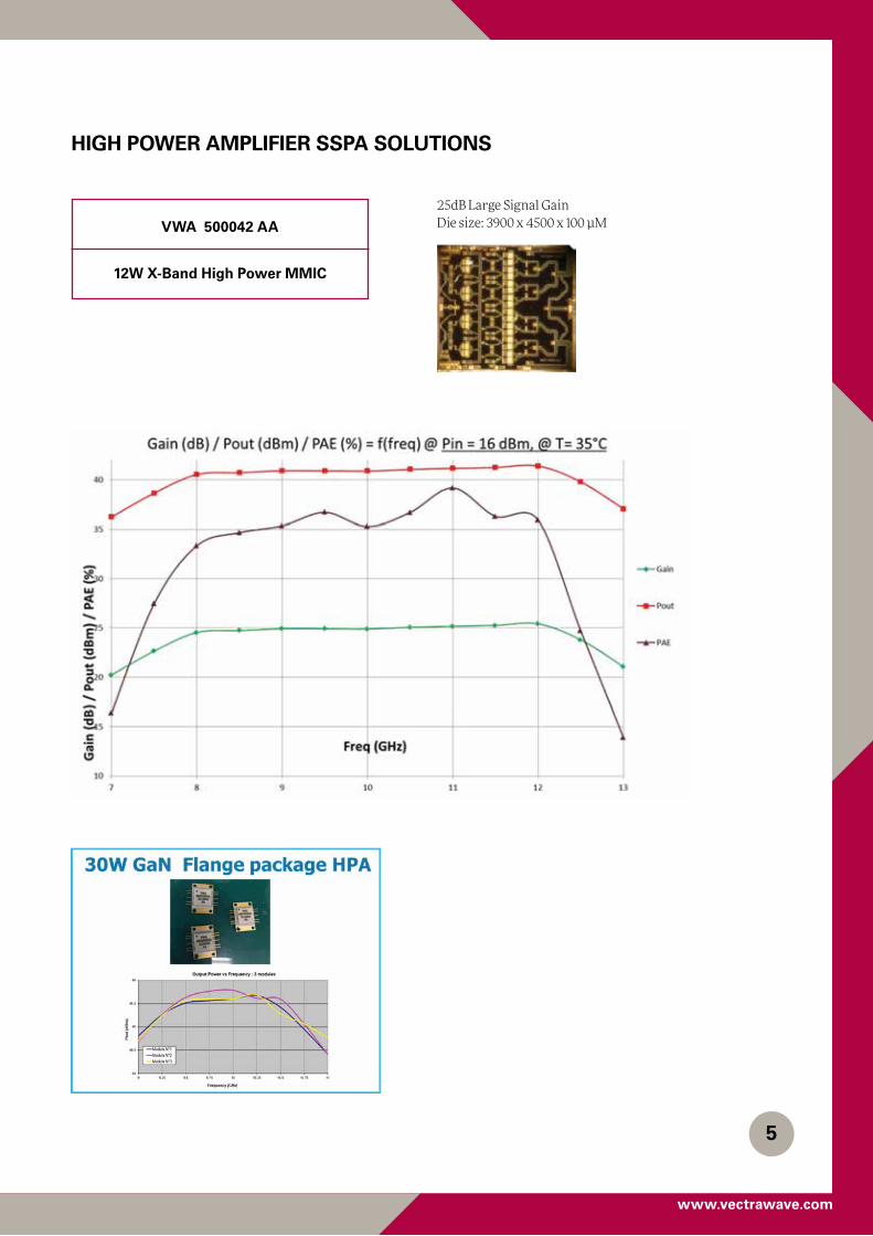
HIGH POWER AMPLIFIER SSPA SOLUTIONS
VWA 500042 AA
12W X-Band High Power MMIC
25dB Large Signal GainDie size: 3900 x 4500 x 100 µM
5
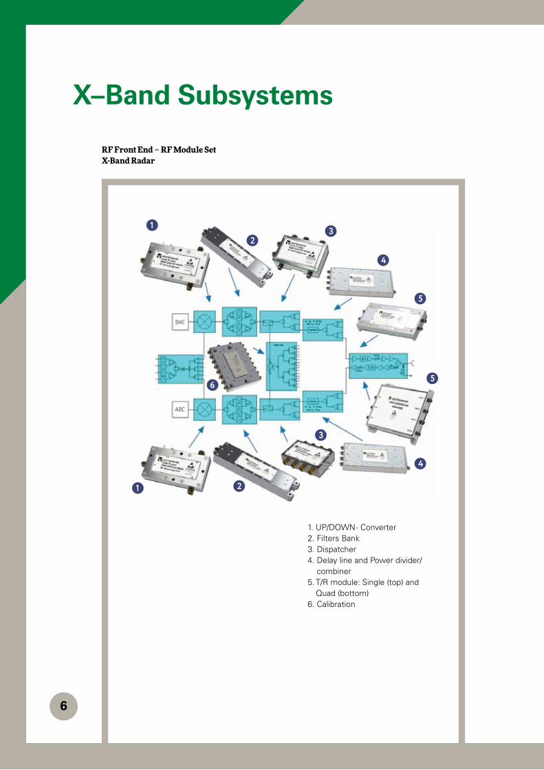
X–Band Subsystems
RF Front End – RF Module SetX-Band Radar
1. UP/DOWN - Converter2. Filters Bank3. Dispatcher4. Delay line and Power divider/
combiner5. T/R module: Single (top) and
Quad (bottom)6. Calibration
1
1
2
2
6
3
3
4
4
5
5
6
www.vectrawave.com
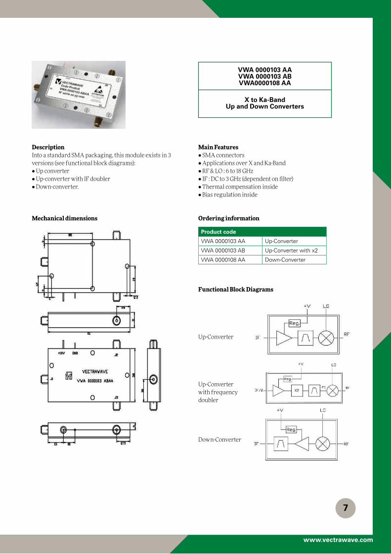
VWA 0000103 AAVWA 0000103 ABVWA0000108 AA
X to Ka-BandUp and Down Converters
DescriptionInto a standard SMA packaging, this module exists in 3versions (see functional block diagrams):• Up converter• Up-converter with IF doubler• Down-converter.
Main Features• SMA connectors• Applications over X and Ka-Band• RF & LO : 6 to 18 GHz• IF : DC to 3 GHz (dependent on filter)• Thermal compensation inside• Bias regulation inside
Up-Converter
Down-Converter
Up-Converterwith frequencydoubler
Ordering information
Functional Block Diagrams
Mechanical dimensions
Product code
VWA 0000103 AA Up-Converter
VWA 0000103 AB Up-Converter with x2
VWA 0000108 AA Down-Converter
7
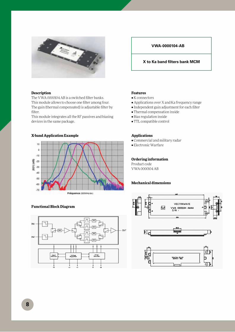
X to Ka band filters bank MCM
DescriptionThe VWA 0000104 AB is a switched filter banks.This module allows to choose one filter among four.The gain (thermal compensated) is adjustable filter by filter.This module integrates all the RF passives and biasing devices in the same package.
Features• K connectors• Applications over X and Ka frequency range• Independent gain adjustment for each filter• Thermal compensation inside• Bias regulation inside• TTL compatible control
Applications• Commercial and military radar• Electronic Warfare
Ordering informationProduct codeVWA 0000104 AB
Functional Block Diagram
Mechanical dimensions
X-band Application Example
VWA-0000104-AB
8

www.vectrawave.com
DescriptionThe 4 and 5 delay lines units (LSB=45ps) exist in two versions : with a 4 ways combiner or with a 4 ways divider.Units with combiner integrate also a 5 bits attenuator (LSB=1dB).Power divider and power combiner are balanced in amplitude (<0.5dB) and phase (<5°).Amplifiers inside offset the losses.
Main Features• K connectors• Applications over X-band• Thermal compensation inside• Bias regulation inside• TTL compatible control• Combiner or divider inside• 5 bits attenuator inside (unit with combiner)
VWA 0000106 AAVWA 0000107 AAVWA 0000507 AAVWA0000506 AA
DELAY LINES
Ordering informationFunctional Block Diagrams
VWA 0000507 AA
VWA 0000506 AA VWA 0000107 AA
VWA 0000106 AA
Product code
VWA 0000106 AAAA 4 bits delay line & divider
VWA 0000107 AAAA Combiner & 4 bits delay line
VWA 0000506 AAAA Combiner & 5 bits delay line
VWA 0000507 AAAA 5 bits delay line & divider
9
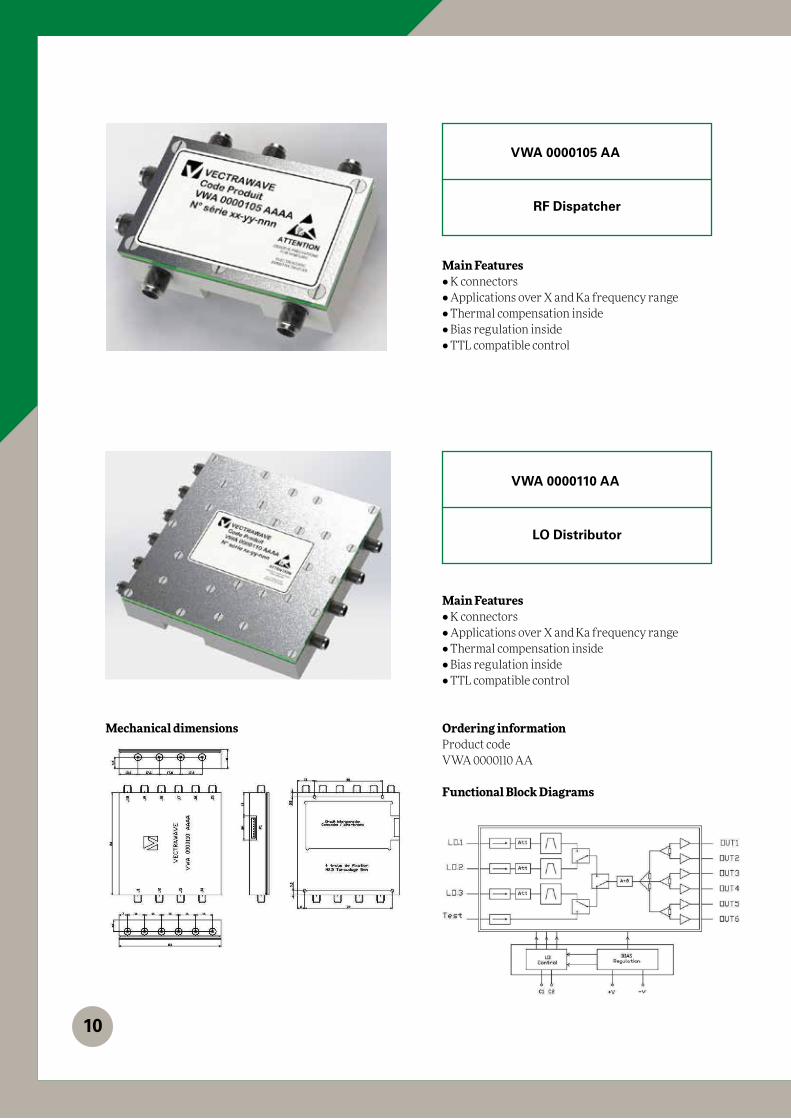
Main Features• K connectors• Applications over X and Ka frequency range• Thermal compensation inside• Bias regulation inside• TTL compatible control
Main Features• K connectors• Applications over X and Ka frequency range• Thermal compensation inside• Bias regulation inside• TTL compatible control
Mechanical dimensions
Functional Block Diagrams
RF Dispatcher
LO Distributor
VWA 0000105 AA
VWA 0000110 AA
Ordering informationProduct codeVWA 0000110 AA
10
www.vectrawave.com
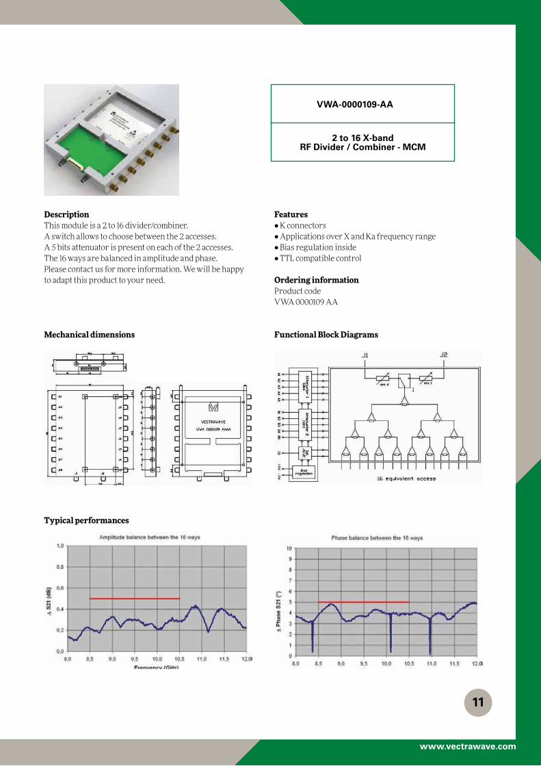
DescriptionThis module is a 2 to 16 divider/combiner.A switch allows to choose between the 2 accesses.A 5 bits attenuator is present on each of the 2 accesses.The 16 ways are balanced in amplitude and phase.Please contact us for more information. We will be happy to adapt this product to your need.
Features• K connectors• Applications over X and Ka frequency range• Bias regulation inside• TTL compatible control
Mechanical dimensions
Typical performances
Functional Block Diagrams
2 to 16 X-bandRF Divider / Combiner - MCM
VWA-0000109-AA
Ordering informationProduct codeVWA 0000109 AA
11
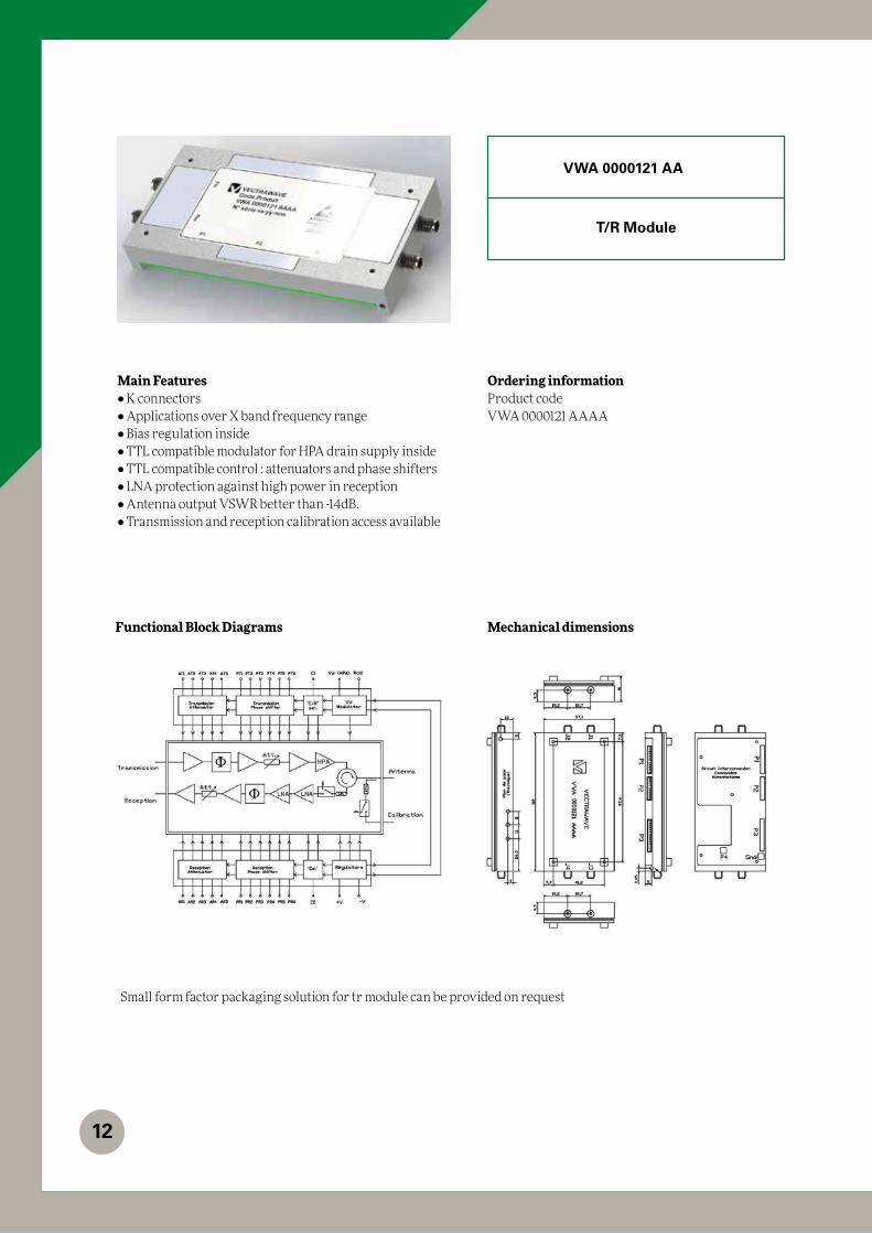
Main Features• K connectors• Applications over X band frequency range• Bias regulation inside• TTL compatible modulator for HPA drain supply inside• TTL compatible control : attenuators and phase shifters• LNA protection against high power in reception• Antenna output VSWR better than -14dB.• Transmission and reception calibration access available
Functional Block Diagrams
T/R Module
VWA 0000121 AA
Ordering informationProduct codeVWA 0000121 AAAA
Mechanical dimensions
Small form factor packaging solution for tr module can be provided on request
12

www.vectrawave.com
Quadri-module (MFC based)
Single Module (DAT & DPS)
13

Ka–Band Subsystems
• Double Stage Up Converter and dual switched SSPA,• Transpose an IF signal (1-1.5GHz) to a Ka-band RF signal
(29.5-31GHz, 3 x Sub bandwidth of 500MHz),• 55dB gain max for a Saturated Output Power to 39dBm,• RS485 Monitoring and Control• Mobile and Satellite Communications Applications
VWA0000687AA – 10W Ka Band Bloc Up Converter
WVA0000688AA-First stage Up-Converter
WVA0000689AA-Second stage Up-Converter
VWA0000690AA – Solid State Power Amplifier
VWA0000687AA – 10W Ka Band Bloc Up Converter
14
WVA0000688AA-First stage Up-Converter
WVA0000689AA-Second stage Up-Converter
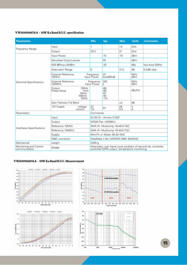
VWA0000687AA – 10W Ka Band B.U.C. specification
Parameters Min Typ Max Units Comments
Frequency RangeInput 1 1.5 GHz
Output 29.5 31 GHz
Electrical Specifications
Input Power -15 -10 dBm
Saturated Output power 39 dBm
IM3 @Pout=34dBm -25 dBc two-tone 5MHz
Attenuator Range 0 31.5 dB 0.5dB step
External Reference Frequency 10MHz Input Power
100±5dB5d8
MHzdBm
External Reference Frequency100MHz Input Power
1002
MHzdBm
Output 100Hz Phase Noise 1kHz 10kHz 100kHz 1MHz
-66-80-81-94-115
dBc/Hz
Gain Flatness Full Band ±3 dB DC Supply voltage current
221.6 24 26
4.5VA
Parameters Comments
Interfaces Specifications
Input K2.92 (f) – Anritsu K102F
Output WR28 Flat - UG599-U
Reference 10MHz SMA (f) - Multicomp 19-49-5-TGC
Reference 100MHz SMA (f) - Multicomp 19-49-5-TGC
Supply Mini-Fit Jr- Molex 39-30-1042M&C connector DataMate L-Tek HARWIN M80- 8420342
Mechanical weight 2300 gMonitoring and Control communication RS485 Attenuator, sub- band Local oscillator of second Up- converter,
switched SSPA output, temperature monitoring
VWA0000687AA – 10W Ka Band B.U.C. Measurement
15
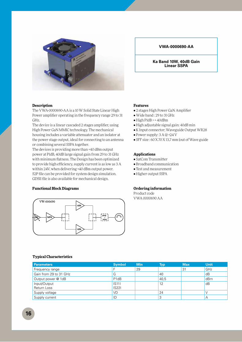
DescriptionThe VWA-0000690-AA is a 10 W Solid State Linear High Power amplifier operating in the frequency range 29 to 31 GHz.The device is a linear cascaded 2 stages amplifier, using High Power GaN MMIC technology. The mechanical housing includes a variable attenuator and an isolator at the power stage output, ideal for connecting to an antenna or combining several SSPA together.The devices is providing more than +40 dBm output power at P1dB, 40dB large signal gain from 29 to 31 GHz with minimum flatness. The Design has been optimized to provide high efficiency, supply current is as low as 3 A within 24V, when delivering +40 dBm output power.S2P file can be provided for system design simulation.GDSII file is also available for mechanical design.
Features• 2 stages High Power GaN Amplifier• Wide band : 29 to 31 GHz• High P1dB > + 40dBm• High adjustable signal gain: 40dB min• K Input connector; Waveguide Output WR28• Power supply: 3 A @ +24 V• SFF size : 60 X 70 X 13,7 mm (out of Wave guide
Applications• SatCom Transmitter• Broadband communication• Test and measurement• Higher output SSPA
Typical Characteristics
Ka Band 10W, 40dB GainLinear SSPA
VWA-0000690-AA
Ordering informationProduct codeVWA 0000690 AA
Functional Block Diagrams
Parameters Symbol Min Typ Max UnitFrequency range F 29 31 GHzGain from 29 to 31 GHz G 40 dBOutput power @ 1dB P1dB 40,5 dBmInput/Output Return Loss
IS11I IS22I
12 dB
Supply voltage VD 24 VSupply current ID 3 A
16
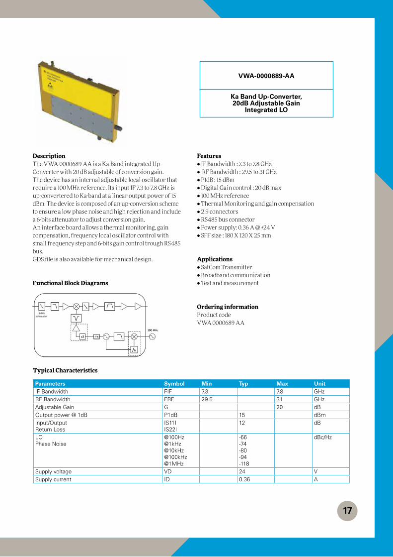
DescriptionThe VWA-0000689-AA is a Ka-Band integrated Up-Converter with 20 dB adjustable of conversion gain.The device has an internal adjustable local oscillator that require a 100 MHz reference. Its input IF 7.3 to 7.8 GHz is up-convertered to Ka-band at a linear output power of 15 dBm. The device is composed of an up-conversion scheme to ensure a low phase noise and high rejection and include a 6-bits attenuator to adjust conversion gain.An interface board allows a thermal monitoring, gain compensation, frequency local oscillator control with small frequency step and 6-bits gain control trough RS485 bus.GDS file is also available for mechanical design.
Features• IF Bandwidth : 7.3 to 7.8 GHz• RF Bandwidth : 29.5 to 31 GHz• P1dB : 15 dBm• Digital Gain control : 20 dB max• 100 MHz reference• Thermal Monitoring and gain compensation• 2.9 connectors• RS485 bus connector• Power supply: 0.36 A @ +24 V• SFF size : 180 X 120 X 25 mm
Applications• SatCom Transmitter• Broadband communication• Test and measurement
Typical Characteristics
Ka Band Up-Converter,20dB Adjustable Gain
Integrated LO
VWA-0000689-AA
Ordering informationProduct codeVWA 0000689 AA
Functional Block Diagrams
Parameters Symbol Min Typ Max UnitIF Bandwidth FIF 7.3 7.8 GHzRF Bandwidth FRF 29.5 31 GHzAdjustable Gain G 20 dBOutput power @ 1dB P1dB 15 dBmInput/Output Return Loss
IS11I IS22I
12 dB
LOPhase Noise
@100Hz@1kHz@10kHz@100kHz@1MHz
-66-74-80-94-118
dBc/Hz
Supply voltage VD 24 VSupply current ID 0.36 A
17
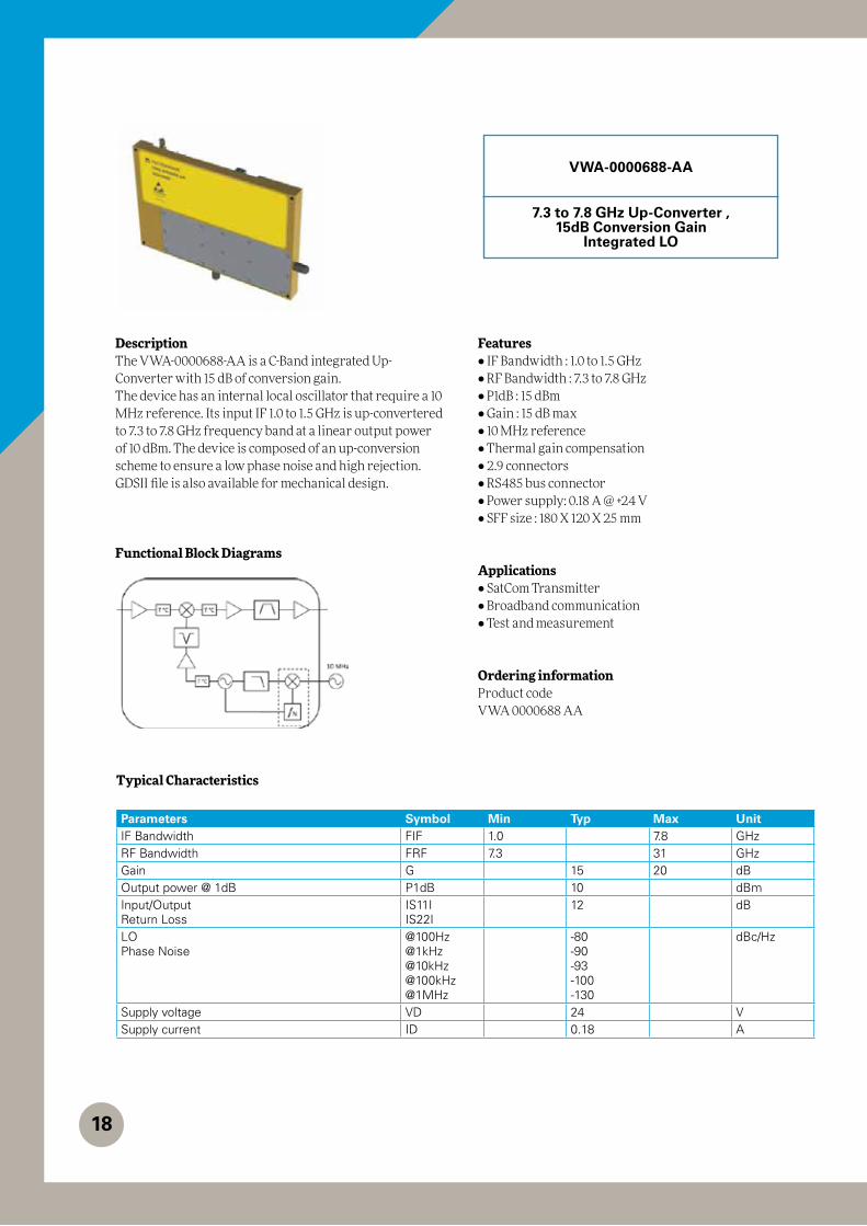
DescriptionThe VWA-0000688-AA is a C-Band integrated Up-Converter with 15 dB of conversion gain.The device has an internal local oscillator that require a 10 MHz reference. Its input IF 1.0 to 1.5 GHz is up-convertered to 7.3 to 7.8 GHz frequency band at a linear output power of 10 dBm. The device is composed of an up-conversion scheme to ensure a low phase noise and high rejection.GDSII file is also available for mechanical design.
Features• IF Bandwidth : 1.0 to 1.5 GHz• RF Bandwidth : 7.3 to 7.8 GHz• P1dB : 15 dBm• Gain : 15 dB max• 10 MHz reference• Thermal gain compensation• 2.9 connectors• RS485 bus connector• Power supply: 0.18 A @ +24 V• SFF size : 180 X 120 X 25 mm
Applications• SatCom Transmitter• Broadband communication• Test and measurement
Typical Characteristics
7.3 to 7.8 GHz Up-Converter ,15dB Conversion Gain
Integrated LO
VWA-0000688-AA
Ordering informationProduct codeVWA 0000688 AA
Functional Block Diagrams
Parameters Symbol Min Typ Max UnitIF Bandwidth FIF 1.0 7.8 GHzRF Bandwidth FRF 7.3 31 GHzGain G 15 20 dBOutput power @ 1dB P1dB 10 dBmInput/Output Return Loss
IS11I IS22I
12 dB
LOPhase Noise
@100Hz@1kHz@10kHz@100kHz@1MHz
-80-90-93-100-130
dBc/Hz
Supply voltage VD 24 VSupply current ID 0.18 A
18

«Providing integrated solution for PAM4 & 400 G Optical links»
Distributed MMIC Amplifier up to 50GHz
Optical Receiver
QFN Drivers up to 40GHz
Dual/Quad Driver for optical transmitter
30KHz to 40 GHz Driver Amplifier
Optical Switch/Amplifier
Optical communication products & subsystems
19
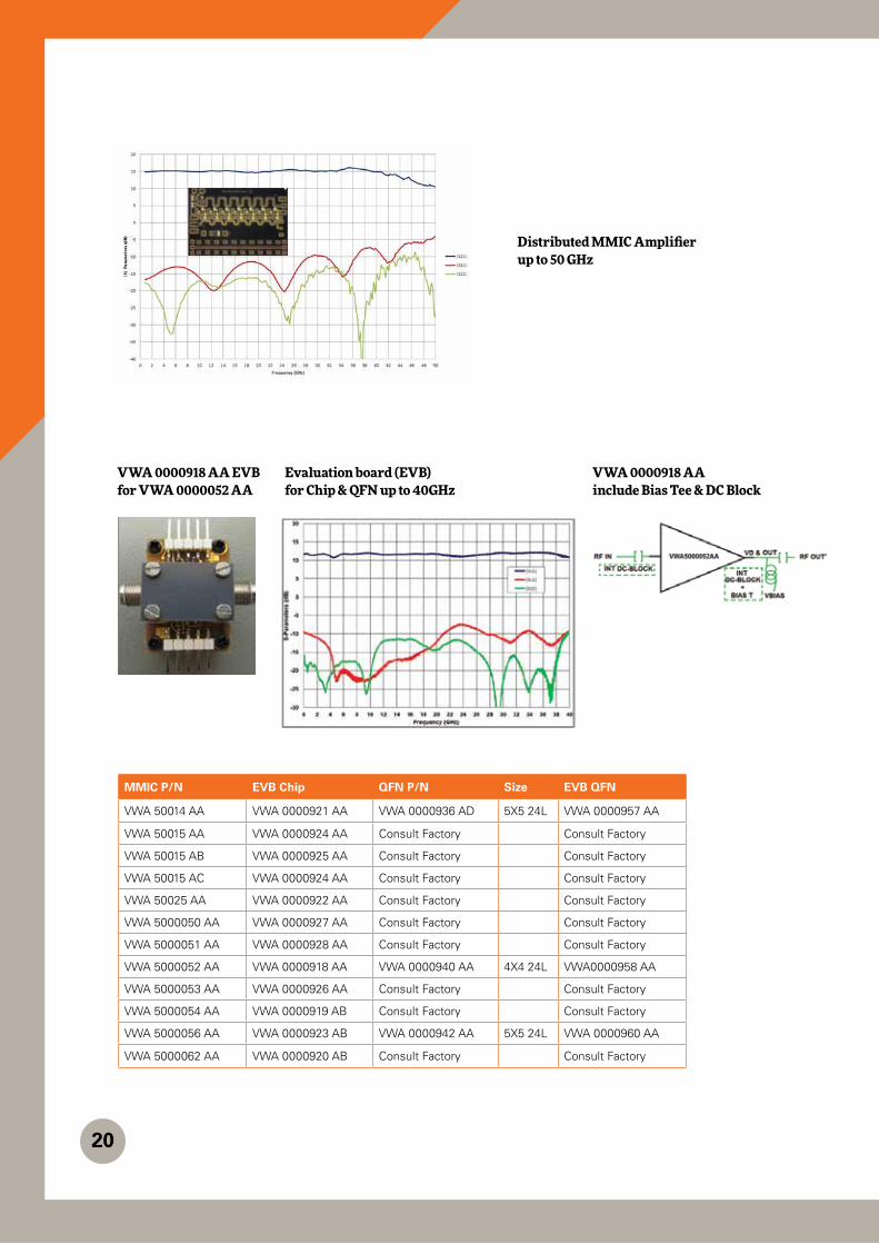
Evaluation board (EVB) for Chip & QFN up to 40GHz
VWA 0000918 AA EVB for VWA 0000052 AA
VWA 0000918 AA include Bias Tee & DC Block
MMIC P/N EVB Chip QFN P/N Size EVB QFN
VWA 50014 AA VWA 0000921 AA VWA 0000936 AD 5X5 24L VWA 0000957 AA
VWA 50015 AA VWA 0000924 AA Consult Factory Consult Factory
VWA 50015 AB VWA 0000925 AA Consult Factory Consult Factory
VWA 50015 AC VWA 0000924 AA Consult Factory Consult Factory
VWA 50025 AA VWA 0000922 AA Consult Factory Consult Factory
VWA 5000050 AA VWA 0000927 AA Consult Factory Consult Factory
VWA 5000051 AA VWA 0000928 AA Consult Factory Consult Factory
VWA 5000052 AA VWA 0000918 AA VWA 0000940 AA 4X4 24L VWA0000958 AA
VWA 5000053 AA VWA 0000926 AA Consult Factory Consult Factory
VWA 5000054 AA VWA 0000919 AB Consult Factory Consult Factory
VWA 5000056 AA VWA 0000923 AB VWA 0000942 AA 5X5 24L VWA 0000960 AA
VWA 5000062 AA VWA 0000920 AB Consult Factory Consult Factory
Distributed MMIC Amplifier up to 50 GHz
20
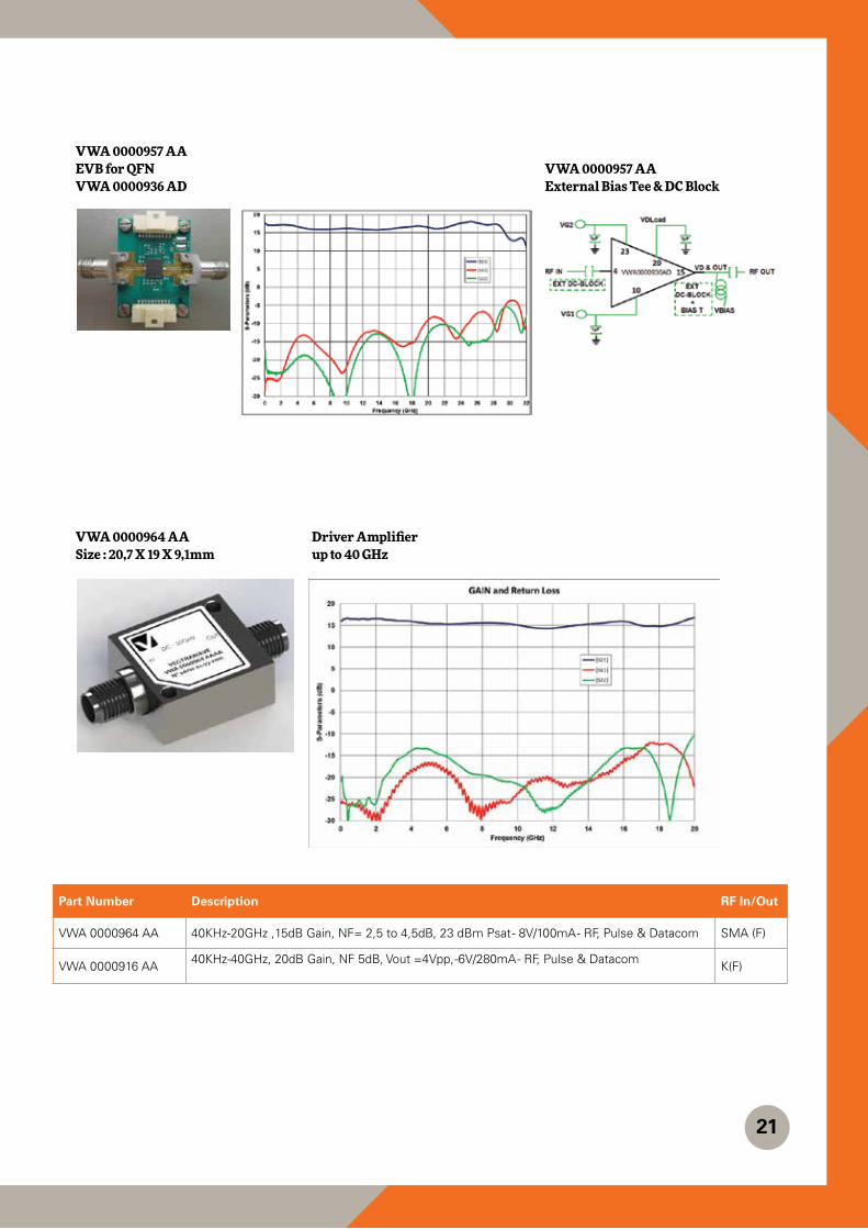
VWA 0000957 AAEVB for QFN VWA 0000936 AD
VWA 0000964 AASize : 20,7 X 19 X 9,1mm
Driver Amplifier up to 40 GHz
VWA 0000957 AA External Bias Tee & DC Block
Part Number Description RF In/Out
VWA 0000964 AA 40KHz-20GHz ,15dB Gain, NF= 2,5 to 4,5dB, 23 dBm Psat - 8V/100mA - RF, Pulse & Datacom SMA (F)
VWA 0000916 AA 40KHz-40GHz, 20dB Gain, NF 5dB, Vout =4Vpp, -6V/280mA - RF, Pulse & Datacom K(F)
21
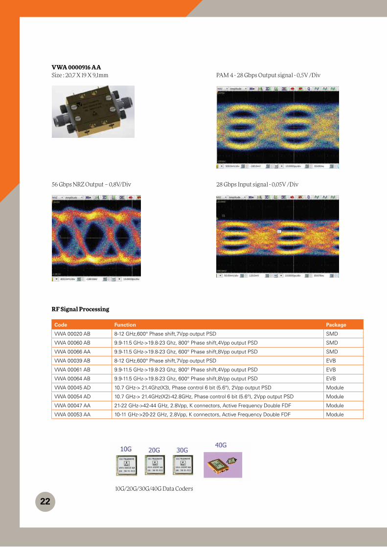
VWA 0000916 AASize : 20,7 X 19 X 9,1mm
56 Gbps NRZ Output – 0,8V/Div
10G/20G/30G/40G Data Coders
PAM 4 - 28 Gbps Output signal - 0,5V /Div
28 Gbps Input signal - 0,05V /Div
Code Function Package
VWA 00020 AB 8-12 GHz,600° Phase shift,7Vpp output PSD SMD
VWA 00060 AB 9.9-11.5 GHz->19.8-23 Ghz, 800° Phase shift,4Vpp output PSD SMD
VWA 00066 AA 9.9-11.5 GHz->19.8-23 Ghz, 600° Phase shift,8Vpp output PSD SMD
VWA 00039 AB 8-12 GHz,600° Phase shift,7Vpp output PSD EVB
VWA 00061 AB 9.9-11.5 GHz->19.8-23 Ghz, 800° Phase shift,4Vpp output PSD EVB
VWA 00064 AB 9.9-11.5 GHz->19.8-23 Ghz, 600° Phase shift,8Vpp output PSD EVB
VWA 00045 AD 10.7 GHz-> 21.4Ghz(X3), Phase control 6 bit (5.6°), 2Vpp output PSD Module
VWA 00054 AD 10.7 GHz-> 21.4GHz(X2)-42.8GHz, Phase control 6 bit (5.6°), 2Vpp output PSD Module
VWA 00047 AA 21-22 GHz->42-44 GHz, 2.8Vpp, K connectors, Active Frequency Double FDF Module
VWA 00053 AA 10-11 GHz->20-22 GHz, 2.8Vpp, K connectors, Active Frequency Double FDF Module
RF Signal Processing
22

Code Function Package
VWA 00020 AB 8-12 GHz,600° Phase shift,7Vpp output PSD SMD
VWA 00060 AB 9.9-11.5 GHz->19.8-23 Ghz, 800° Phase shift,4Vpp output PSD SMD
VWA 00066 AA 9.9-11.5 GHz->19.8-23 Ghz, 600° Phase shift,8Vpp output PSD SMD
VWA 00039 AB 8-12 GHz,600° Phase shift,7Vpp output PSD EVB
VWA 00061 AB 9.9-11.5 GHz->19.8-23 Ghz, 800° Phase shift,4Vpp output PSD EVB
VWA 00064 AB 9.9-11.5 GHz->19.8-23 Ghz, 600° Phase shift,8Vpp output PSD EVB
VWA 00045 AD 10.7 GHz-> 21.4Ghz(X3), Phase control 6 bit (5.6°), 2Vpp output PSD Module
VWA 00054 AD 10.7 GHz-> 21.4GHz(X2)-42.8GHz, Phase control 6 bit (5.6°), 2Vpp output PSD Module
VWA 00047 AA 21-22 GHz->42-44 GHz, 2.8Vpp, K connectors, Active Frequency Double FDF Module
VWA 00053 AA 10-11 GHz->20-22 GHz, 2.8Vpp, K connectors, Active Frequency Double FDF Module
High Speed Logic & Data Coders
Code Function Package
VWA 50001 AA 40 Gbps, 800 mVpp, NRZ to RZ-DPSK coder Die
VWA 50002 AA 40 Gbps, 800 mVpp, D - FF Gate Die
VWA 50023 AA 40 Gbps, 800 mVpp, Differential Coder Die
VWA 50024 AA 40 Gbps, 800 mVpp, NRZ to RZ Coder Die
VWA 50029 AA 40 Gbps, 800 mVpp Duobinary Coder Die
VWA 50030 AA 40 Gbps, 800 mVpp Differential Limiter Amplifier Die
VWA 00055 AA 30 Gbps, 800 mVpp, NRZ to RZ-DPSK coder QFN
VWA 00056 AA 30 Gbps, 800 mVpp, D - FF Gate QFN
VWA 00057 AA 30 Gbps, 800 mVpp, Differential Limiter Amplifier QFN
VWA 00058 AA 30 Gbps, 800 mVpp Duobinary Coder QFN
VWA 00059 AA 30 Gbps, 800 mVpp, NRZ to RZ Coder QFN
VWA 00074 AB 30 Gbps, 800 mVpp, Differential Coder QFN
VWA 00077 AB 30 Gbps, 800 mVpp, GPPO connectors, NRZ to RZ-DPSK coder EVB
VWA 00088 AB 30 Gbps, 800 mVpp, GPPO Connectors, D - FF Gate EVB
VWA 00094 AB 30 Gbps, 800 mVpp, GPPO Connectors, Duobinary Coder EVB
VWA 00095 AB 30 Gbps, 800 mVpp, GPPO Connectors, NRZ to RZ Coder EVB
VWA 00078 AB 30 Gbps, 800 mVpp, GPPO Connectors, Differential Coder EVB
VWA 00075 AB 30 Gbps,GPPO connectors, NRZ to RZ-DPSK Coder with Double Driver 7Vpp EVB
VWA 00068 AB 40 Gbps, 800 mVpp, K connectors, NRZ to RZ-DPSK coder Module
VWA 00069 AB 40 Gbps, 800 mVpp, K Connectors, D - FF Gate Module
VWA 00070 AB 40 Gbps, 800 mVpp, K Connectors, Differential Coder Module
VWA 00071 AB 40 Gbps, 800 mVpp, K Connectors, NRZ to RZ Coder Module
VWA 00072 AB 40 Gbps, 800 mVpp, K Connectors, Duobinary Coder Module
VWA 00087 AB 40 Gbps, 800 mVpp, K Connectors, Differential Limiter Amplifier Module
23
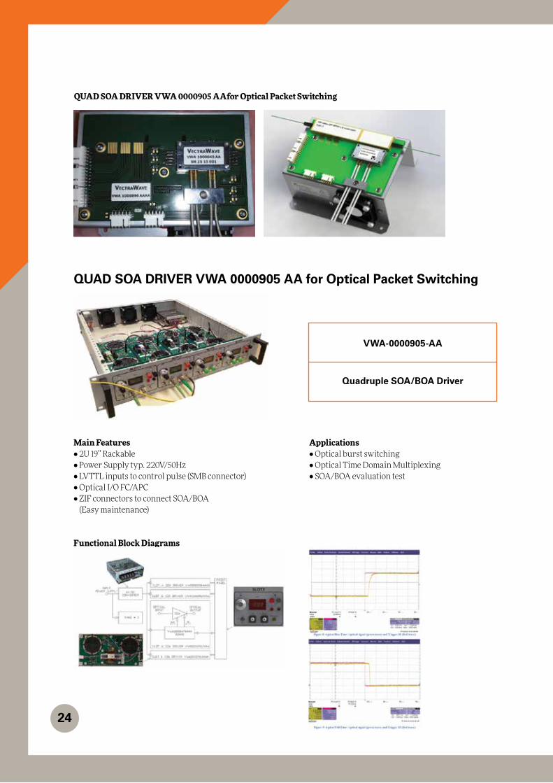
QUAD SOA DRIVER VWA 0000905 AA for Optical Packet Switching
Main Features• 2U 19’’ Rackable• Power Supply typ. 220V/50Hz• LVTTL inputs to control pulse (SMB connector)• Optical I/O FC/APC• ZIF connectors to connect SOA/BOA
(Easy maintenance)
Applications• Optical burst switching• Optical Time Domain Multiplexing• SOA/BOA evaluation test
Quadruple SOA/BOA Driver
VWA-0000905-AA
Functional Block Diagrams
QUAD SOA DRIVER VWA 0000905 AAfor Optical Packet Switching
24
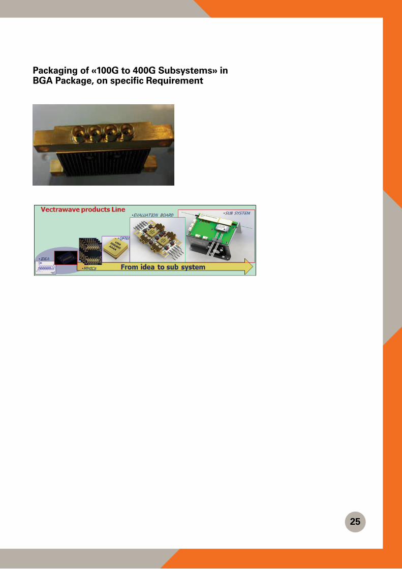
Packaging of «100G to 400G Subsystems» in BGA Package, on specific Requirement
25
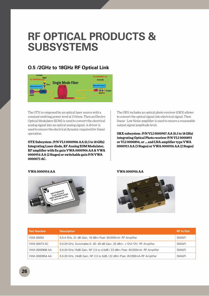
O.5 /2GHz to 18GHz RF Optical Link
RF OPTICAL PRODUCTS & SUBSYSTEMS
The OTX is composed by an optical laser source with a constant emitting power level at 1550nm. Then an Electro Optical Modulator (EOM) is used to convert the electrical analog signal into an optical analog signal. A driver is used to ensure the electrical dynamic required for linear operation. OTX Subsystem : P/N VLI 0000906 AA (0,5 to 18 GHz) Integrating Laser diode, RF Analog EOM Modulator, RF amplifier with fix gain VWA 0000906 AA & VWA 0000954 AA (2 Stages) or switchable gain P/N VWA 0000073 AC.
The ORX includes an optical photo receiver (ORX) allows to convert the optical signal into electrical signal. Then linear Low Noise amplifier is used to ensure a reasonable output signal amplitude level.
ORX subsystem : P/N VLI 0000907 AA (0,5 to 18 GHz) integrating Optical Photo receiver P/N VLI 0000893 or VLI 0000894, or .., and LNA amplifier type VWA 0000913 AA (3 Stages) or VWA 0000916 AA (2 Stages)
VWA 0000954 AA VWA 0000916 AA
Part Number Description RF In/Out
VWA 00052 0,5-4 GHz ,31 dB Gain, 18 dBm Psat - 9V/200mA - RF Amplifier SMA(F)
VWA 00073 AC 0,5-20 GHz, Switchable 0 - 20 - 40 dB Gain, 20 dBm - +12V/-12V - RF Amplifier SMA(F)
VWA 0000906 AA 0,5-20 GHz,15dB Gain, NF 2,5 to 4,5dB / 23 dBm Psat - 9V/200mA - RF Amplifier SMA(F)
VWA 0000954 AA 0,5-20 GHz, 24dB Gain, NF 2,5 to 5dB / 22 dBm Psat - 8V/290mA -RF Amplifier SMA(F)
26
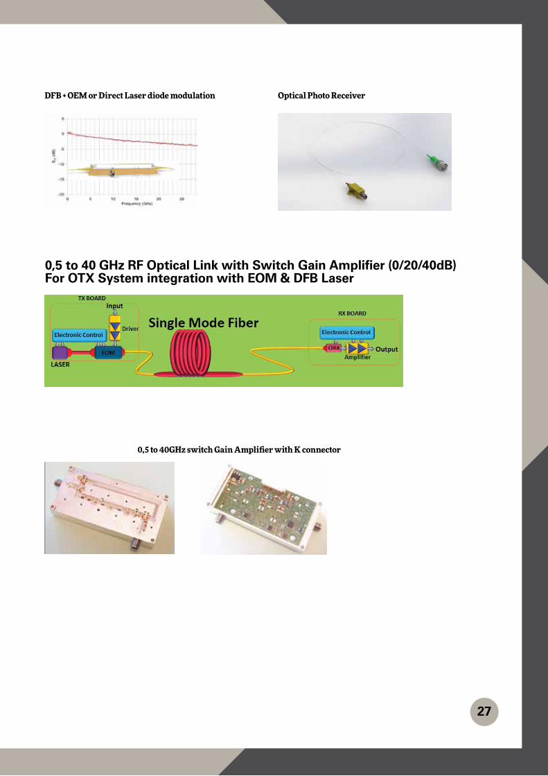
0,5 to 40 GHz RF Optical Link with Switch Gain Amplifier (0/20/40dB)For OTX System integration with EOM & DFB Laser
DFB + OEM or Direct Laser diode modulation
0,5 to 40GHz switch Gain Amplifier with K connector
Optical Photo Receiver
Part Number Description RF In/Out
VWA 00052 0,5-4 GHz ,31 dB Gain, 18 dBm Psat - 9V/200mA - RF Amplifier SMA(F)
VWA 00073 AC 0,5-20 GHz, Switchable 0 - 20 - 40 dB Gain, 20 dBm - +12V/-12V - RF Amplifier SMA(F)
VWA 0000906 AA 0,5-20 GHz,15dB Gain, NF 2,5 to 4,5dB / 23 dBm Psat - 9V/200mA - RF Amplifier SMA(F)
VWA 0000954 AA 0,5-20 GHz, 24dB Gain, NF 2,5 to 5dB / 22 dBm Psat - 8V/290mA -RF Amplifier SMA(F)
27
Micro strip Pin Optical Receiver
Optical Receiver with K connector
Optical Receiver with coplanar PIN
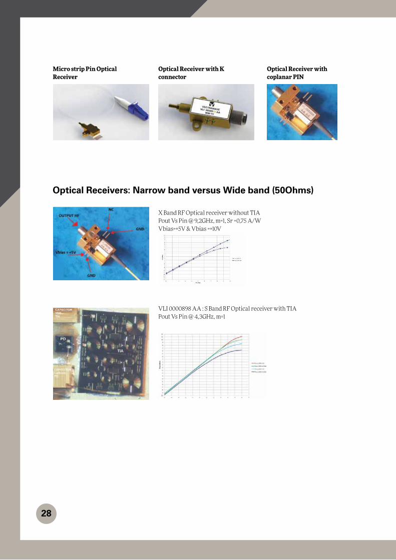
Optical Receivers: Narrow band versus Wide band (50Ohms)
X Band RF Optical receiver without TIAPout Vs Pin @ 9,2GHz, m=1, Sr =0,75 A/W Vbias=+5V & Vbias =+10V
VLI 0000898 AA : S Band RF Optical receiver with TIAPout Vs Pin @ 4,3GHz, m=1
28
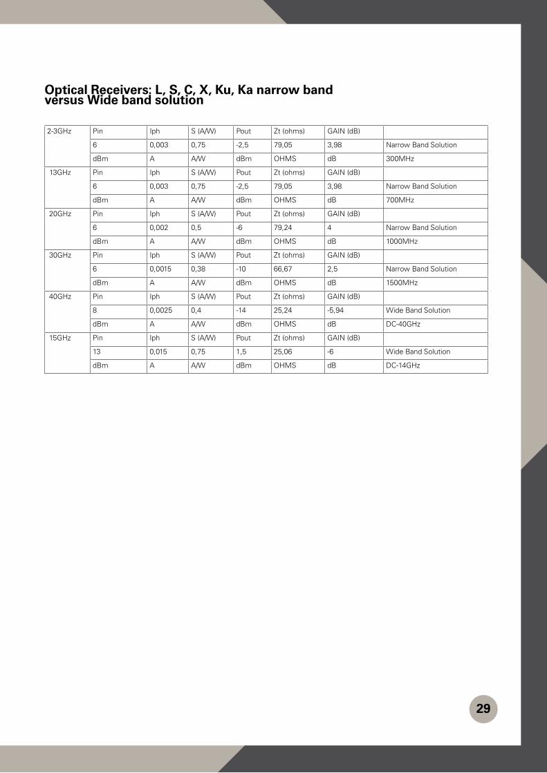
2-3GHz
Pin Iph S (A/W) Pout Zt (ohms) GAIN (dB)
6 0,003 0,75 -2,5 79,05 3,98 Narrow Band Solution
dBm A A/W dBm OHMS dB 300MHz
13GHz
Pin Iph S (A/W) Pout Zt (ohms) GAIN (dB)
6 0,003 0,75 -2,5 79,05 3,98 Narrow Band Solution
dBm A A/W dBm OHMS dB 700MHz
20GHz
Pin Iph S (A/W) Pout Zt (ohms) GAIN (dB)
6 0,002 0,5 -6 79,24 4 Narrow Band Solution
dBm A A/W dBm OHMS dB 1000MHz
30GHz
Pin Iph S (A/W) Pout Zt (ohms) GAIN (dB)
6 0,0015 0,38 -10 66,67 2,5 Narrow Band Solution
dBm A A/W dBm OHMS dB 1500MHz
40GHz
Pin Iph S (A/W) Pout Zt (ohms) GAIN (dB)
8 0,0025 0,4 -14 25,24 -5,94 Wide Band Solution
dBm A A/W dBm OHMS dB DC-40GHz
15GHz
Pin Iph S (A/W) Pout Zt (ohms) GAIN (dB)
13 0,015 0,75 1,5 25,06 -6 Wide Band Solution
dBm A A/W dBm OHMS dB DC-14GHz
Optical Receivers: L, S, C, X, Ku, Ka narrow band versus Wide band solution
29

Lannion office : 4, Rue André Marie Ampère - 22300 LannionHead office : Rue de la Croix Blanche, Immeuble LOGI - 78350 Les Loges en Josas – FranceAsia Office : 4F 123 AnMei St. NeiHu – Taipei – 11484 – Taiwan - Tel: +886 2 8791 7699
[email protected] +33 (0)619 870 560
www.vectrawave.com