2015/9/4System Arch 2008 (Fire Tom Wada) 1 SEMICONDUCTOR TECHNOLOGY -CMOS- Fire Tom Wada.
29
22/03/13 System Arch 2008 (Fire Tom Wada) 1 SEMICONDUCTOR TECHNOLOGY -CMOS- Fire Tom Wada
-
Upload
dylan-sullivan -
Category
Documents
-
view
234 -
download
0
Transcript of 2015/9/4System Arch 2008 (Fire Tom Wada) 1 SEMICONDUCTOR TECHNOLOGY -CMOS- Fire Tom Wada.

23/04/19System Arch 2008 (Fire Tom
Wada) 1
SEMICONDUCTOR TECHNOLOGY-CMOS-
Fire Tom Wada

23/04/19 System Arch 2008 (Fire Tom Wada) 2
What is semiconductor and LSIs
Huge number of transistors can be integrated in a small Si chip.
The size of the chip is roughly the size of nails.
Currently, 10M transistors can be integrated.
1000 times integration comparing to 20 yrs ago.
The cost of the chip is roughly same. All electronic equipments are powered by
LSIs. PCs, Cellular phones, 3D graphics,
Internet.

23/04/19 System Arch 2008 (Fire Tom Wada) 3
PC mother board
Large Scale Integration

23/04/19 System Arch 2008 (Fire Tom Wada) 4
SONY PLAYSTATION 2 MAINBOARD
Rendering LSI
High Speed Memory
Graphics LSI
Direct RDRAM

23/04/19 System Arch 2008 (Fire Tom Wada) 5
Mobile Phone MainboardMobile Phone MainboardMemory, Logic,
Analog

23/04/19 System Arch 2008 (Fire Tom Wada) 6
Key device is LSI
INTEL Pentium III module

23/04/19 System Arch 2008 (Fire Tom Wada) 7
This is a packaged LSI-Pentium III 300MHz Cache LSI-
15 mm
20 mm

23/04/19 System Arch 2008 (Fire Tom Wada) 8
Si chip is molded in the package.
2 million transistor Chip is connected to the pins thru
wires.

23/04/19 System Arch 2008 (Fire Tom Wada) 9
6 inches Si wafer

23/04/19 System Arch 2008 (Fire Tom Wada) 10
8 inches Si wafer
Hundreds of Chips
on a Si
Wafer

23/04/19 System Arch 2008 (Fire Tom Wada) 11
Several hundreds of chips are fabricated on a wafer simultaneously.

23/04/19 System Arch 2008 (Fire Tom Wada) 12
Chip photo- Motion Estimation Chip for HDTV camera -
9.1 mm
8.6 mm
Your small
finger’s nail size.
200M transistor
s.

23/04/19 System Arch 2008 (Fire Tom Wada) 13
Scanning Electron Microscope photo- Cross-section of the LSI -
0.5 micron

23/04/19 System Arch 2008 (Fire Tom Wada) 14
Structure Of CMOS LSI
Isolation PN-Isolation, Local oxidation
Si Substrate Bulk, epitaxial , SOI
Well Structure N-type well in P-type Substrate
Latch Up PNP Bipolar Transistor and NPN Bipolar Transistor
Fabrication Process Technology

23/04/19 System Arch 2008 (Fire Tom Wada) 15
Cross-section of the LSI
P-type Si substrateN-type well
N+ N+ P+ P+
Metal wiring
Poly-silicon
Poly-silicon
N-type MOS transistor
P-type MOS transistor
Si wafer

23/04/19 System Arch 2008 (Fire Tom Wada) 16
Transistor module ( FEP)
65nmLithography(VUV, EPL) Mask
CMPplanarization
Low Resistance Contact withHigh Aspect ratio
High κGate insulator
Fine Cu interconnectLow κ
interdielectric
SiGe/Metal gate
Multi-level Metalization
Module( BEP)
Low Resistance Ultra shallow junction
Low stress Shallow Trench Isolation
Advanced Process Development

23/04/19 System Arch 2008 (Fire Tom Wada) 17
LSI integration trend- Moore’s law -
Wide-TV, PHS Wide-TV, PHS phonephone
DVD player
DVD-ROM
DVD-RAMDVD recorder
Source: SEMATEC
81
10B
1B
100M
10M
1M
100K
10K
1K83 85 87 89 91 93 95 97 99 01 03 05 07 09
0.8 0.5 0.3 0.18
CHANNEL LENGTH (MICRON)
0.13
Digital HDTV receiver
Nu
mb
er
of
tran
sis
tors
on
a
ch
ip
The number of transistors are
increasing by 58% per year.
- Moore’s Law -
23/04/19 System Arch 2008 (Fire Tom Wada) 18
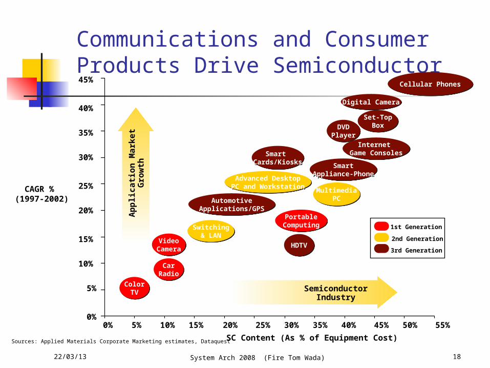
Communications and Consumer Products Drive Semiconductor
Sources: Applied Materials Corporate Marketing estimates, Dataquest
35%
30%
25%
20%
15%
10%
5%
0%0% 5% 10% 15% 20% 25% 30% 35%
CAGR % (1997-2002)
SemiconductorIndustry
Ap
plicati
on
Mark
et
Gro
wth
SC Content (As % of Equipment Cost)
3rd Generation
2nd Generation
1st Generation
ColorTV
ColorTV
CarRadioCar
Radio
VideoCameraVideo
Camera
PortableComputingPortable
ComputingSwitching& LAN
Switching& LAN
HDTVHDTV
MultimediaPC
MultimediaPC
Advanced DesktopPC and WorkstationAdvanced Desktop
PC and Workstation
AutomotiveApplications/GPS
AutomotiveApplications/GPS
DVDPlayerDVD
Player
Set-TopBox
Set-TopBox
Internet Game Consoles
Internet Game ConsolesSmart
Cards/KiosksSmart
Cards/KiosksSmart
Appliance-PhoneSmart
Appliance-Phone
Digital CameraDigital Camera
40% 45% 50% 55%
40%
45%Cellular PhonesCellular Phones

23/04/19 System Arch 2008 (Fire Tom Wada) 19
Fabrication Process Issues
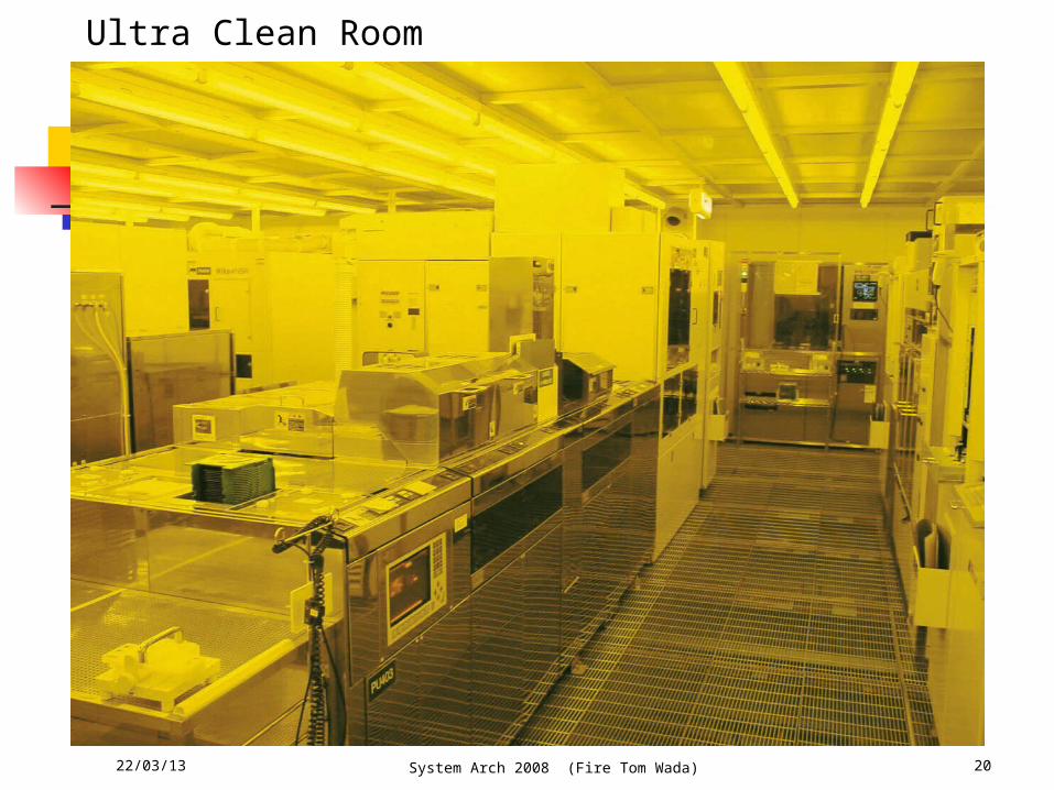
23/04/19 System Arch 2008 (Fire Tom Wada) 20
Ultra Clean Room
23/04/19 System Arch 2008 (Fire Tom Wada) 21
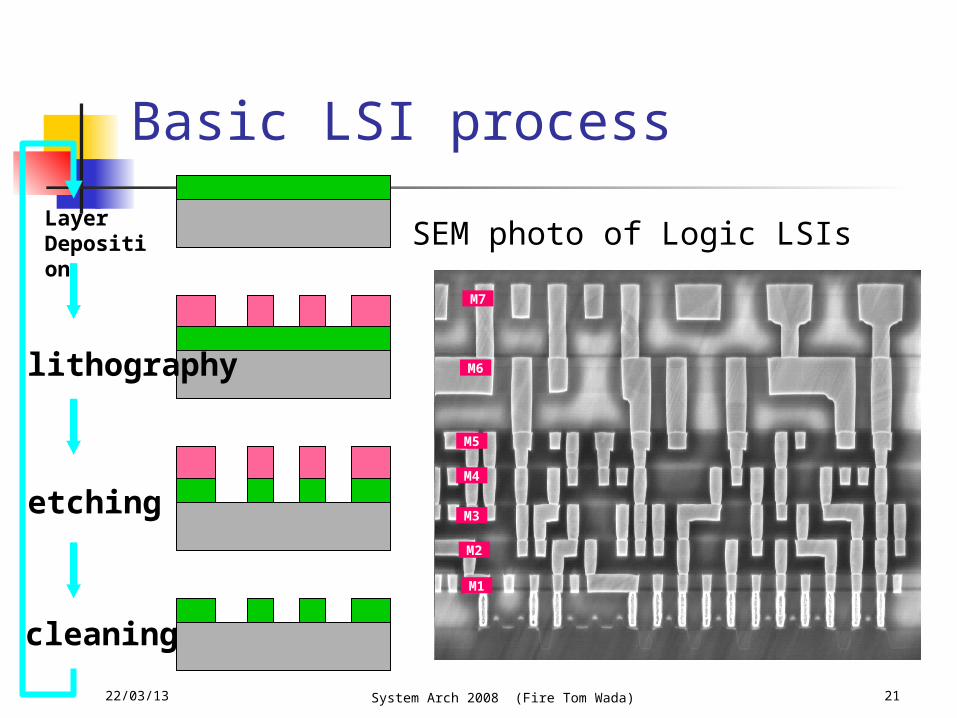
Basic LSI process
Layer Deposition
lithography
etching
cleaning
M1
M2
M3
M4
M5
M6
M7
SEM photo of Logic LSIs

23/04/19 System Arch 2008 (Fire Tom Wada) 22
Projection
A A A A A A A A A A A A A A A A A A A A A A A A A A A A A A A A A A A A A A A A
Lens
Si Wafer
Mask
Lens
Light Source
X
Y
Stage

23/04/19 System Arch 2008 (Fire Tom Wada) 23
Wafer Test
scribing
Chips
Mounting
Bonding
Enclosing
marking
Final Test I
Burn-In
Ex.)Vcc:7V , Temp.:125 , 24℃ ~ 42hrs
Remove Process defect Chips
Functional Test , DC TestA
ssem
bly
Flo
w
Shipping TestFinal Test II
Packaging & Test
Sample
Wafer
Functional Test , DC/AC Test
Functional Test(at Speed) , DC/AC Test
Pre Test
Testing

23/04/19 System Arch 2008 (Fire Tom Wada) 24
Large Scale Integration
NMOS , PMOS and Wiring All Logic Function can be made Memory Element Can be made
Billions of Transistors and wiring make LSI!

23/04/19 System Arch 2008 (Fire Tom Wada) 25
CMOS NOT (Inverter)

23/04/19 System Arch 2008 (Fire Tom Wada) 26
CMOS NAND と NORA B f
0 0 1
0 1 1
1 0 1
1 1 0
A B f
0 0 1
0 1 0
1 0 0
1 1 0

23/04/19 System Arch 2008 (Fire Tom Wada) 27
Classification Of LSI
1. Logic LSI: Micro Processor, Digital Signal Processor (DSP), FPGA2. Memory LSI: RAM (DRAM, SRAM), ROM (Flash Memory)3. Analog LSI: ADC, DAC, Filter, Amplifier
Micro Processor (PC’s central processing Unit) Perform Digital computation according to the program in Memory Integration in 7000 times in 25 years, (Moor’s Law) Clock Speed : 700 times in 25 years
Memory LSI: Dynamic Random Access Memory: Main memory for Computer, 4-
times density in 4 years Static Random Access Memory : work memory for mobile
equipments Flash Memory : Nonvolatile memory , Digital Camera Storage
Analog LSI: Used for interface, high speed RF interface, Analog to Digital
Conversion, Digital to Analog Conversion

23/04/19 System Arch 2008 (Fire Tom Wada) 28
Analog to Digital Conversion
ADC LSI
Analog to Digital
Sample the analog wave
Convert to Digital format in Binary
Same as f(t) to AnContinuous time
Discrete time

23/04/19 System Arch 2008 (Fire Tom Wada) 29
SoC Flash Memory
Chip photo