2015 NEPP ETW - Reliability of Class-Y Packages in focus ... - Fri/1100 - NEPP... · JPL and...
31
Reliability of Class-Y Packages in focus of Xilinx V4/V5 and Aeroflex packages Jong-ook Suh [email protected] 818-354-4574 Jet Propulsion Laboratory, California Institute of Technology NASA Electronic Parts and Packaging Program (NEPP) 2015 Annual NEPP Electronic Technology Workshop (ETW) June 26th, 2015 1
Transcript of 2015 NEPP ETW - Reliability of Class-Y Packages in focus ... - Fri/1100 - NEPP... · JPL and...

Reliability of Class-Y Packages in focus of Xilinx V4/V5
and Aeroflex packages
Jong-ook Suh
818-354-4574
Jet Propulsion Laboratory, California Institute of Technology
NASA Electronic Parts and Packaging Program (NEPP)
2015 Annual NEPP Electronic Technology Workshop (ETW)
June 26th, 2015
1

Background
2To be presented by Jong-ook Suh at the NASA NEPP Electronics Technology Workshop (ETW), Greenbelt, MD, June 23-25, 2015
Class-Y packages : Non-hermetic ceramic flip chip packages
Underfill and heat spread attach material are exposed to outside environment.
• Direct attachment of heat spread to die for better thermal management.
• Easy to mount capacitors close to the die.
Xilinx CF package (before 2014) Xilinx CN Package (2014)
Package Assembly IBM Bromont, Canada Kyocera / Six Sigma
Heat spread SiC (non-conductive) Al-SiC (Conductive)
Heat spread corner pillar None 4 corner pillars
Heat spread attach material (TIM1) Electrically conductive Electrically non-conductive
Flip chip bump 95Pb5Sn Sn63Pb37
Underfill IBM proprietary Xilinx proprietary
Solder Columns IBM CLASP column
(90Pb10Sn)
Six Sigma column (80Pb20Sn
with Cu spiral)
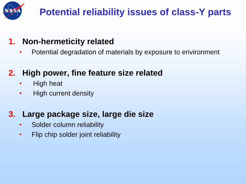
Potential reliability issues of class-Y parts
1. Non-hermeticity related
• Potential degradation of materials by exposure to environment
2. High power, fine feature size related
• High heat
• High current density
3. Large package size, large die size
• Solder column reliability
• Flip chip solder joint reliability
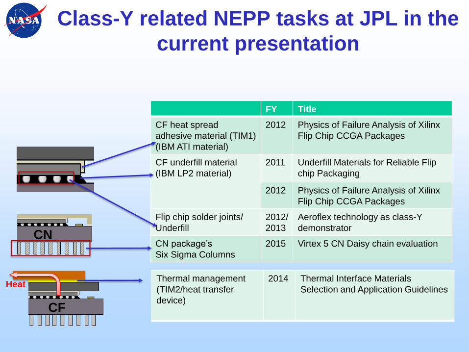
Thermal management
(TIM2/heat transfer
device)
2014 Thermal Interface Materials
Selection and Application Guidelines
Class-Y related NEPP tasks at JPL in the
current presentation
FY Title
CF heat spread
adhesive material (TIM1)
(IBM ATI material)
2012 Physics of Failure Analysis of Xilinx
Flip Chip CCGA Packages
CF underfill material
(IBM LP2 material)
2011 Underfill Materials for Reliable Flip
chip Packaging
2012 Physics of Failure Analysis of Xilinx
Flip Chip CCGA Packages
Flip chip solder joints/
Underfill
2012/
2013
Aeroflex technology as class-Y
demonstrator
CN package’s
Six Sigma Columns
2015 Virtex 5 CN Daisy chain evaluationCN
CF
Heat

Underfill and TIM1 study
Motivation:
Potential degradation of underfill and TIM1 by exposure to environment
Procedure:
• Raw materials of the CF package (LP2 & ATI) were procured from IBM during FY11 and
FY12.
(Raw materials of the CN package are currently being procured. Xilinx has provided raw material
information to Shri Agarwal at JPL.)
• Assessed and rated the potential risks of various constituents of the LEO environment to
the reliabilities of the materials prior to experiments.
• Ionizing radiation, UV radiation: Mitigated by shielding practices. Not strong enough to
deteriorate underfill and TIM1 materials.
• Atomic oxygen (ATOX) : Only low energy ATOX inside spacecraft. No direct ATOX
impingement.
• Long term vacuum exposure
• Humidity
• Exposed cured samples to various types of environment for extended time.
TIM1
Underfill
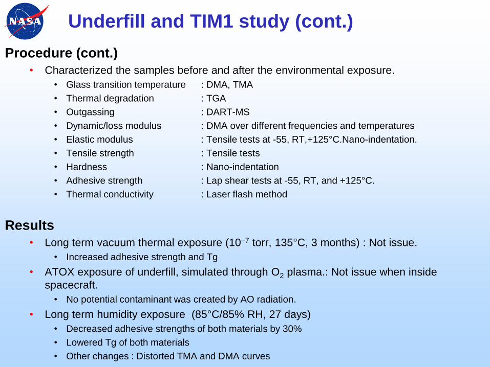
Underfill and TIM1 study (cont.)
Procedure (cont.)
• Characterized the samples before and after the environmental exposure.
• Glass transition temperature : DMA, TMA
• Thermal degradation : TGA
• Outgassing : DART-MS
• Dynamic/loss modulus : DMA over different frequencies and temperatures
• Elastic modulus : Tensile tests at -55, RT,+125°C.Nano-indentation.
• Tensile strength : Tensile tests
• Hardness : Nano-indentation
• Adhesive strength : Lap shear tests at -55, RT, and +125°C.
• Thermal conductivity : Laser flash method
Results
• Long term vacuum thermal exposure (10–7 torr, 135°C, 3 months) : Not issue.
• Increased adhesive strength and Tg
• ATOX exposure of underfill, simulated through O2 plasma.: Not issue when inside
spacecraft.
• No potential contaminant was created by AO radiation.
• Long term humidity exposure (85°C/85% RH, 27 days)
• Decreased adhesive strengths of both materials by 30%
• Lowered Tg of both materials
• Other changes : Distorted TMA and DMA curves

Flip chip solder interconnection reliability
JPL and Aeroflex performed a collaborative study on reliability of class-Y
packages.
• Aeroflex has been qualifying their packaging technology for Class-Y parts.
• Aeroflex supplied its R&D samples to JPL. Flip chip on ceramic substrate with daisy chained
flip chip bumps. No columns.
Aeroflex sample
Component Aeroflex Sample Xilinx CN Package Xilinx CF Package
Die Dimension 15 x 15x 0.7mm 25x 18x 1 mm 25x18x1mm
Under Bump Metallurgy (UBM) Al/Ni(V)/Cu (Typical sputtered) Ti/Cu/Ni Ti/Cu/Ni (Typical electroplated)
Underfill Material Aeroflex proprietary Kyocera proprietary LP2 material; IBM proprietary.
Flip chip Solder Bump Material Sn63Pb37 (Tm=183˚C) Sn63Pb37 (Tm=183˚C) 95Pb5Sn (Tm= 308~312 ˚ C)
Substrate/Carrier Multilayer ceramic Multilayer ceramic Multilayer ceramic
Flip chip passivation opening
size
80 μm ~80 μm ~80 μm
UBM Diameter 102 µm ~105 µm ~105 µm
Flip chip Solder Bump height
(assembled)
~80 μm ~90 μm ~90 μm
Flip chip Solder Bump width ~150 μm ~150 μm ~150 μm
Flip chip Solder Bump pitch size 254 μm ~250 μm ~250 μm
Die
Substrate

• Samples were pre-conditioned and temperature cycled.
• Long term vacuum thermal aging
(IBM underfill material exhibited improved properties after long term vacuum thermal aging.)
• Long term humidity exposure
(IBM underfill showed 30% reduction in adhesive strength, reduced Tg.. )
• Multiple reflow
• Sn63 bumps will reflow during the subsequent reflow process.
– Both Aeroflex and Xilinx CN packages have Sn63 flip chip solder bumps.
– Xilinx CF package had 95Pb high-Pb flip chip solder bumps.
• Current stressing
• Electromigration reduces the solder joint strength.
• Test conditions
• No pre-conditioning (control) Temp cycling (-55/125°C)
• Long term vacuum thermal aging (10–7 torr, 135°C, 3 months) Temp cycling
• Long term humidity exposure (85°C/85%, 27 days) Temp cycling
• Multiple reflow (5x reflows) Temp cycling
• Current stressing (96 hours, 2 x 10⁴ A/cm2 at 110°C, Package : RT) Temp cycling
8
Flip chip solder joint interconnection reliability (cont.)
• Results
• Vacuum thermal aging and multiple reflow improved temp cycling life, almost by 50%.
• Humidity exposure reduced temp cycling life, almost by 30%
• Current stressing did not affect the temp cycling life.
Precondition Weibull Life Weibull Slope Weibull Fit R2
Baseline (no precondition) 3629 6.3 0.9613
Vacuum Thermal aging (10–7 torr, 135°C, 3 months) 5474 8.9 0.9402
Humidity exposure (85°C/85%, 27 days) 2438 7.5 0.9717
Multiple reflow (5X reflows) 5237 6.4 0.9348
Current stressing ( 96 hours, 2 x 10⁴ A/cm2 at 110°C) 3978 4.9 0.8013
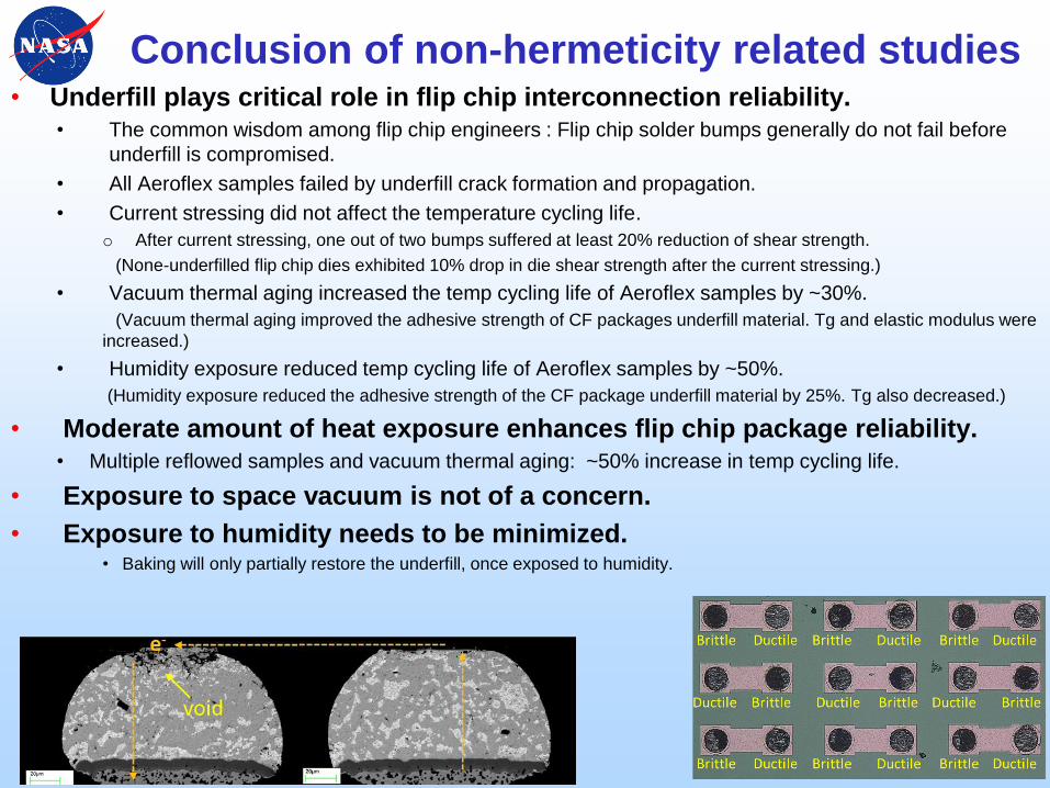
• Underfill plays critical role in flip chip interconnection reliability. • The common wisdom among flip chip engineers : Flip chip solder bumps generally do not fail before
underfill is compromised.
• All Aeroflex samples failed by underfill crack formation and propagation.
• Current stressing did not affect the temperature cycling life.
o After current stressing, one out of two bumps suffered at least 20% reduction of shear strength.
(None-underfilled flip chip dies exhibited 10% drop in die shear strength after the current stressing.)
• Vacuum thermal aging increased the temp cycling life of Aeroflex samples by ~30%.
(Vacuum thermal aging improved the adhesive strength of CF packages underfill material. Tg and elastic modulus were
increased.)
• Humidity exposure reduced temp cycling life of Aeroflex samples by ~50%.
(Humidity exposure reduced the adhesive strength of the CF package underfill material by 25%. Tg also decreased.)
• Moderate amount of heat exposure enhances flip chip package reliability.• Multiple reflowed samples and vacuum thermal aging: ~50% increase in temp cycling life.
• Exposure to space vacuum is not of a concern.
• Exposure to humidity needs to be minimized.• Baking will only partially restore the underfill, once exposed to humidity.
Conclusion of non-hermeticity related studies

The adhesive strength of TIM1 material and
thermal management scheme
40
50
60
70
80
90
100
110
120
0 5 10 15 20 25
Junction temperature
TIM2 temperature
*Assumed 65°C at the chassis mounting
V5 power disspation (W)
Te
mp
era
ture
(°C
)
−55°C +22°C at +125°C
Lap shear strength (psi) 1985 2061 631
Lap shear strength of the TIM1 material of Xilinx CF package
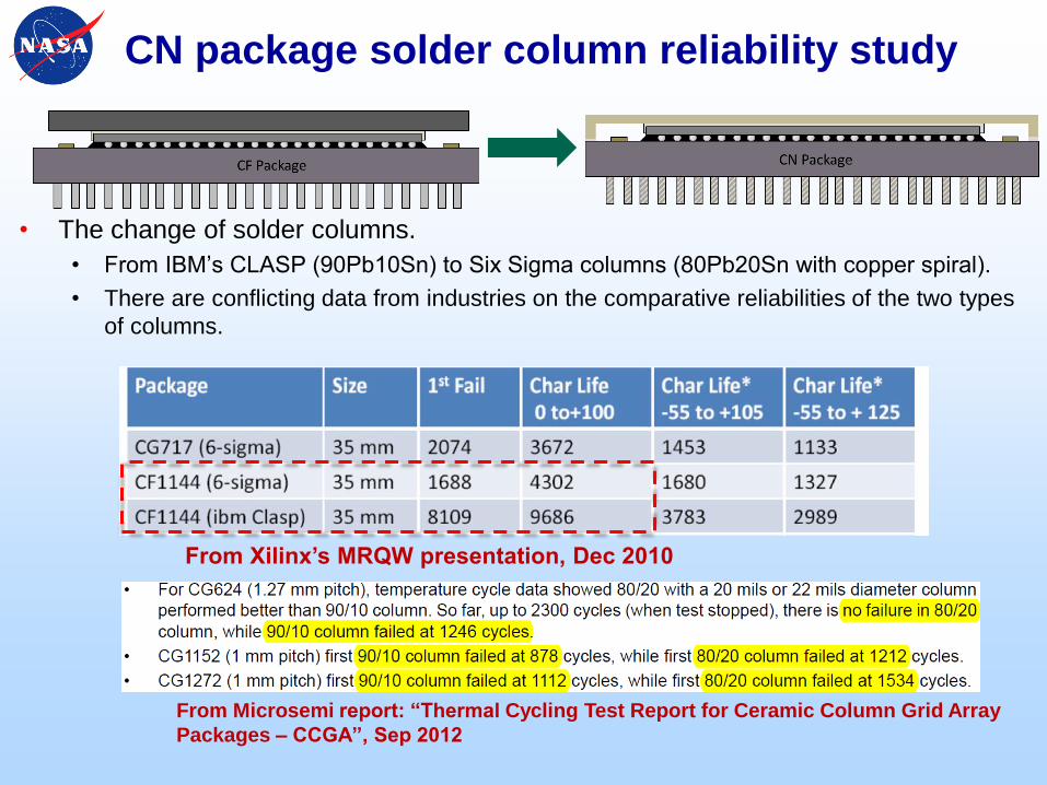
CN package solder column reliability study
• The change of solder columns.
• From IBM’s CLASP (90Pb10Sn) to Six Sigma columns (80Pb20Sn with copper spiral).
• There are conflicting data from industries on the comparative reliabilities of the two types
of columns.
From Xilinx’s MRQW presentation, Dec 2010
From Microsemi report: “Thermal Cycling Test Report for Ceramic Column Grid Array
Packages – CCGA”, Sep 2012
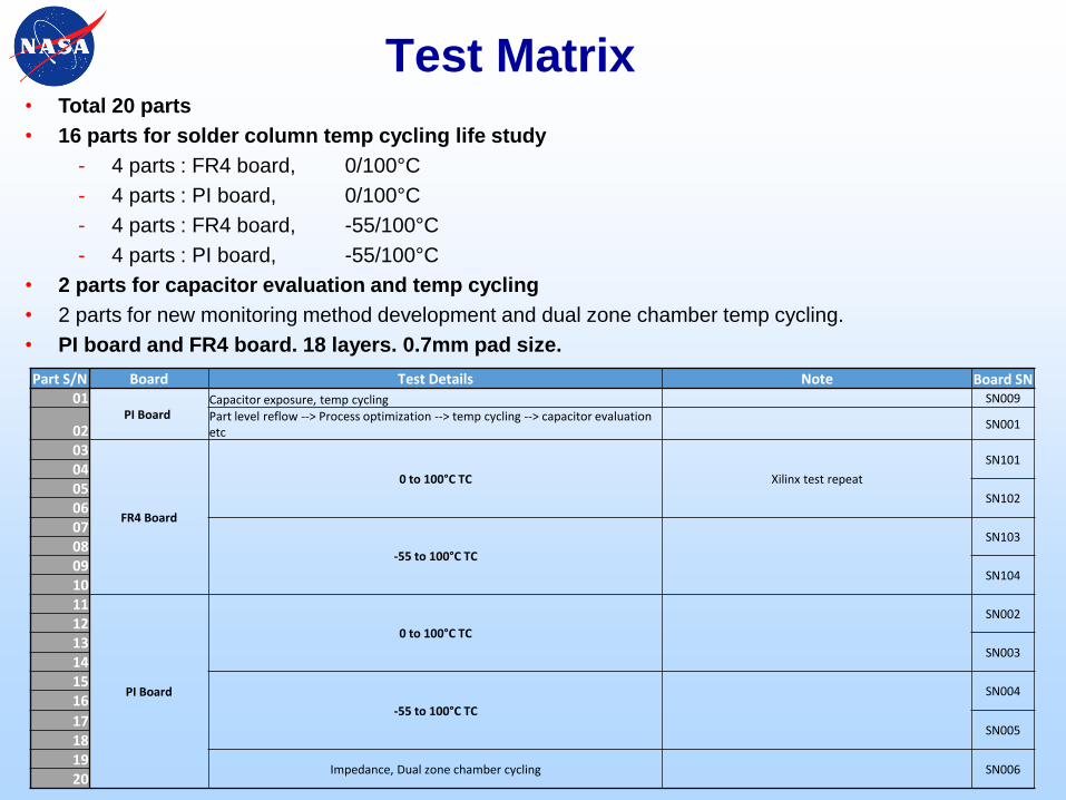
Test Matrix• Total 20 parts
• 16 parts for solder column temp cycling life study
- 4 parts : FR4 board, 0/100°C
- 4 parts : PI board, 0/100°C
- 4 parts : FR4 board, -55/100°C
- 4 parts : PI board, -55/100°C
• 2 parts for capacitor evaluation and temp cycling
• 2 parts for new monitoring method development and dual zone chamber temp cycling.
• PI board and FR4 board. 18 layers. 0.7mm pad size.
Part S/N Board Test Details Note Board SN01
PI BoardCapacitor exposure, temp cycling SN009
02Part level reflow --> Process optimization --> temp cycling --> capacitor evaluation etc
SN001
03
FR4 Board
0 to 100°C TC Xilinx test repeat
SN1010405
SN1020607
-55 to 100°C TC
SN1030809
SN1041011
PI Board
0 to 100°C TC
SN0021213
SN0031415
-55 to 100°C TC
SN00416
17SN005
1819
Impedance, Dual zone chamber cycling SN00620
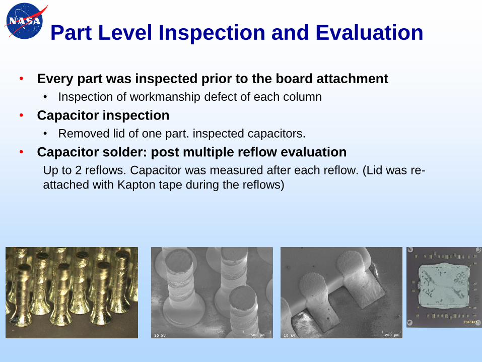
Part Level Inspection and Evaluation
• Every part was inspected prior to the board attachment
• Inspection of workmanship defect of each column
• Capacitor inspection
• Removed lid of one part. inspected capacitors.
• Capacitor solder: post multiple reflow evaluation
Up to 2 reflows. Capacitor was measured after each reflow. (Lid was re-
attached with Kapton tape during the reflows)

Test Board Assembly• Pad/solder mask opening size and board finish are same as the Xilinx
test board
• Two V5s per board
• Two types of resin materials:
- Polyimide (IPC 4041/41)
- FR4 (IPC 4041/26)
• Seven daisy chains per V5
- Each corners, outer 2 rows, next 3 rows, and all internal rows.

0 20 40 60 80 100
0
20
40
60
80
100
Temperature cycling
16
0 to 100°C, 10 min ramp, 10 min dwell.
327 cycles.
Time (min)
Te
mp
(°C
)
0 20 40 60 80 100
4
8
12
16
20
24
28
32
36
Time (min)
Oh
m
4 Corner daisy chains
Outer 2 rows
Next 3 rows
All internal rows
-55 to 100°C, 47 min ramp, 10 min dwell.
54 cycles.
Tem
p (
°C)
Time (min)50 100 150 200
-60
-40
-20
0
20
40
60
80
100
Time (min)
Oh
m
4 corner daisy chains
Outer 2 rows
Next 3 rows
All internal rows
50 100 150 200
5
10
15
20
25
30
17
Synergistic aspects with other NEPP task at JPL
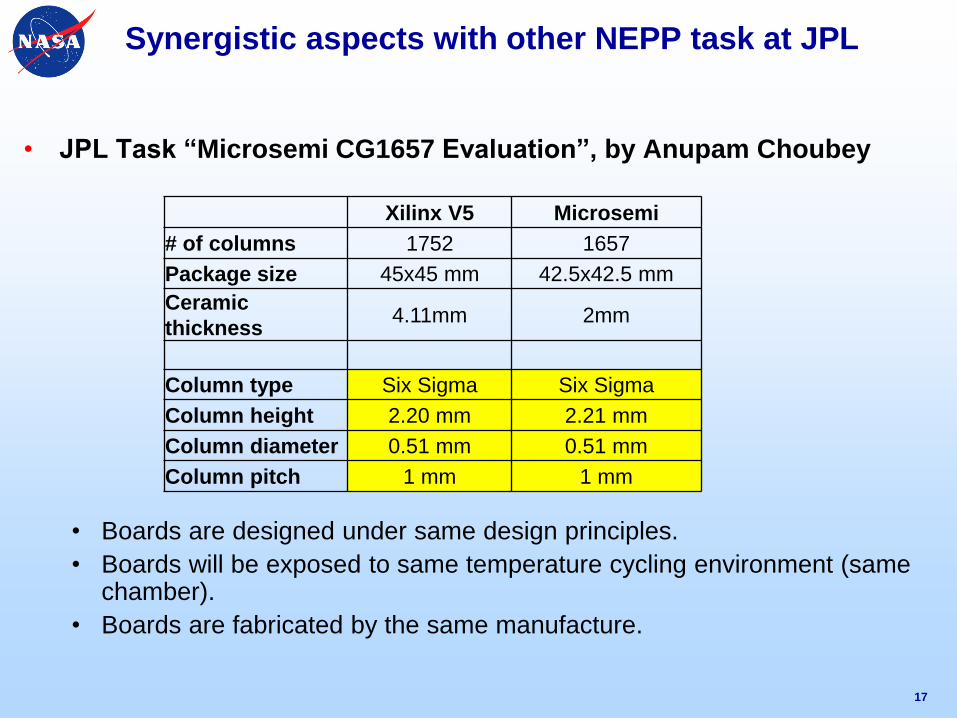
• JPL Task “Microsemi CG1657 Evaluation”, by Anupam Choubey
• Boards are designed under same design principles.
• Boards will be exposed to same temperature cycling environment (same chamber).
• Boards are fabricated by the same manufacture.
Xilinx V5 Microsemi
# of columns 1752 1657
Package size 45x45 mm 42.5x42.5 mm
Ceramic
thickness4.11mm 2mm
Column type Six Sigma Six Sigma
Column height 2.20 mm 2.21 mm
Column diameter 0.51 mm 0.51 mm
Column pitch 1 mm 1 mm

Related documents
• Jong-ook Suh, R. Peter Dillon, “Xilinx V4 Package Reliability: Properties and Reliability of
LP2 Underfill”, NEPP report, 2012.
• Jong-ook Suh, “Physics of Failure Analysis of Xilinx Flip Chip CCGA Packages: Effects
of Mission Environments on Properties of LP2 Underfill and ATI Lid Adhesive
Materials”, NEPP report, 2013.
• Jong-ook Suh, Scott Popelar, Shri Agarwal, “Aeroflex Technology as Class-Y
Demonstrator”, NEPP report, 2014
• Jong-ook Suh, R. Peter Dillon, Stephen Tseng, “ Thermal Interface Materials Selection and
Application Guidelines: In Perspective of Xilinx Virtex-5QV Thermal Management”,
NEPP report, in release process.
18

Microsemi CG1657 Evaluation
19
–RTG4 Die
PME 0508 2
terminal
capacitors
placed inside
Under fill
Thermal adhesive between die and seal lid
Kovar Lid
Microsemi
Microsemi
CG1657 (flip chip): 1657 columns, 1mm pitch
• Die size: 23 mm x 24 mm x 675 um
• Package weight: 28.8 grams
• Package size: 42.5 mm square
• Package height: 5.42 mm
Anupam [email protected]
818-354-0522

Optical Images
20
2.21
mm
1 mm

Capacitor Revision (Change from AVX to
Presidio)
21
Current Cap Revised Version
Manufacturer AVX (X7R) Presidio (X7R)
Electrode BME (Nickel) PME (Silver Palladium)
Voltage 6.3V and 4V 6.3V
Capacitance 2.2 ± 20%
0.68 ± 20%
0.18 uF ± 10%
Dissipation Factor 5% max. (for 10V) 7.5% (MIL-PRF-Thin)
Thermal
Conductivity
4-5 W/m K 6W/mK
Terminations Plated Ni and
Solder
NT9 (Ni + 90%Sn-
10%Pb)
L x W x T (mm) 2.03 x 1.27 x 0.96 0.05 x 0.08 x 0.017
Inductance 55 to 65 pH 110 to 130 pH range
Metallization Band 0.005 min band
0.02 min space
AVX Inter-
digitated
Capacitor
Presidio Low
Inductance
Capacitor

Package Internal View
22

Elemental Composition External
Package
23
–Au
Plating
–Ni-
Au
–Ni-
Au
–Alumi
na
–Alumi
na
–Ni-
Au–Ni-
Au–Au
Plating
–Kovar Lid
–Alumina Substrate
1. Kovar ring is braze
to ceramic with Ag-
Cu – Braze alloy
2. Then Kovar lid is
seam seal to Kovar
ring
3. Ni-Au plating is final
step
–Au plating
–Ni plating
Solder Columns
24
Cu
Bright
areas
are Pb

EDX Elemental Mapping
25
–Sn-Cu
Map–Pb Map
–C
u–S
n
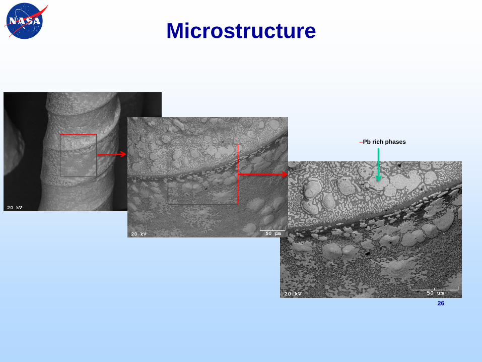
Microstructure
26
–Pb rich phases

Thermal Shock Results
27
Level Number Mean Std Dev Std Err Mean Lower 95% Upper 95%
TCT 0 28 0.435714 0.048795 0.00922 0.41679 0.45464
TCT 250 28 0.421429 0.041786 0.00790 0.40523 0.43763
TCT 400 28 0.425000 0.044096 0.00833 0.40790 0.44210
• Component level thermal shock
performed to investigate any
anomalies under thermal shock
• Thermal shock conditions
(-55C to 125C), Ramp < 2 min, 10 min
dwell
• No significant increase in resistance
observed
• Next step: Mount the package onto
PCB and thermal cycle
Target resistance for individual pin pairs: 0.4 Ohms
+ −
Resistance Probes (0.4
Ohms)

28
Presidio Capacitor (PME) - Electrode Silver, PalladiumDielectric – Barium Titanium oxide
Ag
Pd
Ba, Ti
O
Pd, Ag Electrode
Barium Titanium Oxide dielectric
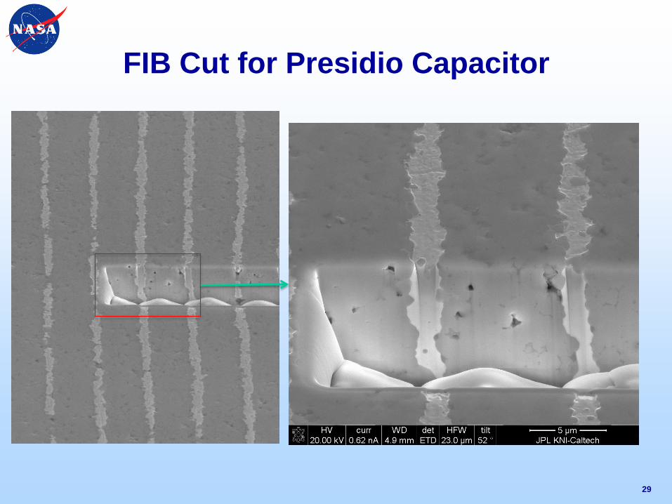
29
FIB Cut for Presidio Capacitor
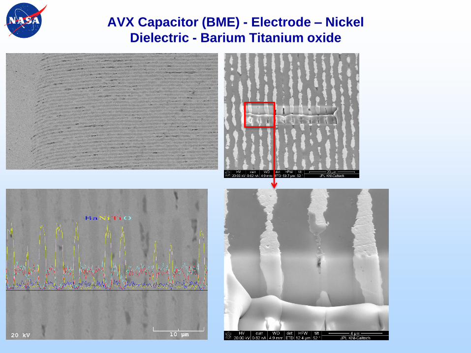
AVX Capacitor (BME) - Electrode – Nickel
Dielectric - Barium Titanium oxide

Mechanical Package Model
Solidworks Model: Daniel
Lamadrid, JPL Summer Intern