2015 HOMO and LUMO evaluation, biomedical applications, etc. 8) Technologies of organic electronics:...
124
2 nd International Fall School on Organic Electronics Book of abstracts September 20-25, 2015 Moscow region, Russia Soyuz Hotel www.ispm.ru/ifsoe-2015 IFSOE 2015
-
Upload
phunghuong -
Category
Documents
-
view
216 -
download
1
Transcript of 2015 HOMO and LUMO evaluation, biomedical applications, etc. 8) Technologies of organic electronics:...

2nd International Fall School on Organic Electronics
Book of abstracts
September 20-25, 2015Moscow region, Russia
Soyuz Hotelwww.ispm.ru/ifsoe-2015
I FS O E2 0 1 5

2
2nd INTERNATIONAL FALL SCHOOL ON ORGANIC ELECTRONICS – 2015 (IFSOE-2015)
OrganizersDivision of Chemistry and Material Science of Russian Academy of Sciences
Enikolopov Institute of Synthetic Polymeric Materials of Russian Academy of Sciences (ISPM RAS)
Lomonosov Moscow State University (MSU)
Russian Science Foundation (RSF)
Russian Foundation for Basic Research (RFBR)
Federal Agency of Scientific Organizations
Scientific program1) Fundamentals of organic electronics: charge transport, modeling, photophysics, etc.
2) Materials for organic electronics: organic conductors and semiconductors, dielectrics, substrates, etc.
3) Organic field-effect transistors: single crystal, polymer and monolayer OFETs, integrated circuits and related devices.
4) Organic light-emitting devices: OLEDs and OLETs, white light-emitting devices, TADF devices, organic lasers.
5) Organic and hybrid solar cells: small molecules and polymer photovoltaics, tandem cells, perovskites-based photovoltaics, etc.
6) Organic sensors: physical (pressure, temperature, photo, etc.) sensors, chemo- and biosensors.
7) Characterization techniques: various spectroscopy, microscopy, and x-ray scattering techniques, charge mobility measurements, thermal and surface analysis, HOMO and LUMO evaluation, biomedical applications, etc.
8) Technologies of organic electronics: printing of organic materials and devices, roll-to-roll techniques, ink formulations, encapsulation, etc.

3
School ChairsProf. Sergey Ponomarenko (Enikolopov Institute of Synthetic Polymeric Materials of RAS, Russia)Prof. Dmitry Paraschuk (Lomonosov Moscow State University, Russia)
International Advisory BoardProf. Vladimir Agranovich (Institute for Spectroscopy RAS, Russia)Prof. Mikhail Alfimov (Photochemistry Center of RAS, Russia)Prof. Paul Berger (Ohio State University, USA)Prof. Christoph Brabec (University Erlangen-Nürnberg, Germany)Prof. Sergei Chvalun (National Research Center “Kurchatov Institute”, Russia)Prof. Vladimir Dyakonov (University of Würzburg, Germany)Prof. Antonio Facchetti (Northwestern University, USA)Prof. Sir Richard Friend (University of Cambridge, UK)Prof. Marcus Halik (University Erlangen-Nürnberg, Germany)Dr. Stephan Kirchmeyer (Heraeus Precious Metals GmbH, Germany)Prof. Alexei Khokhlov (Lomonosov Moscow State University, Russia)Prof. Guglielmo Lanzani (Politechnico di Milano, Italy)Prof. Dmitrii Perepichka (McGill University, Canada)Prof. Maxim Pshenichnikov (University of Groningen, the Netherlands)Dr. Abderrahim Yassar (Ecole polytechnique, France)
Local Organizing CommitteeAlexey Sizov – workshop secretaryDr. Elena AginaAskold Trul
Technical PartnerProfessional Congress Organizer – UniFest CongressProject Coordinator – Tatiana Volkova

School-conference program

IFSOE-2015 Time Schedule
SundaySeptember 20th
MondaySeptember 21th
TuesdaySeptember 22th
WednesdaySeptember 23th
ThursdaySeptember 24th
FridaySeptember 25th
Conference School
9:00Dago de Leeuw Jean Roncali Luisa Torsi Ma Dongge
Alexey Komolov 9:00Mikhail Vener
10:00
Visit to Moscow
Kremlin and Russian
Diamond Fund
(optional)
Lunch
Registration at ISPM
RAS
16:00 departure to
Conference Site
Johannes Gierschner Vladimir Dyakonov Fabio Biscarini Antonio FacchettiViktor Ivanov 10:00
Sergey Novikov11:00 Coffee-break Closing ceremony.
Dmitry Paraschuk11:00
Aldo Di Carlo Valerii Kobryanskii Paul BergerPavel Troshin
12:00 Artem Bakulin 12:00
Martijn Kemerink Dimitri Ivanov Stephan KirchmeyerDmitry Godovsky
13:00 Albert Nasibulin 13:00
Lunch14:00 14:00
Conference
15:00
Oral Talks 1 Oral Talks 2 Oral Talks 4
Trip to New Jerusalem (optional)
Departure 15:00
16:00 16:00
Coffee-break
17:00Hotel arrival.
RegistrationPoster session 1 Oral Talks 3 Poster sesion 2
17:00
18:00 18:00
19:00Dinner
Conference dinner
Dinner19:00
School
Sport activities (swimming pool,
wellness, spa)
Moscow sightseeing tour
Sport activities (swimming pool,
wellness, spa)
20:00 School opening.
Christoph Brabec
20:00
21:00 21:00
Welcome-party22:00-22:30 22:00-22:30

6
Sunday, September 20th
10:00 – 16:00 Visit to Moscow Kremlin (optional) Registration at ISPM RAS. Departure to conference site
19:00 – 20:00 Dinner
20:00 – 20:15 School opening
20:15 – 21:15 T-1. Christoph Brabec. Principal failure and degradation mechanisms of organic semiconductors
21:15 – 22:30 Welcome-party
Monday, September 21st
8:00 – 9:00 Breakfast
Chair: Christoph Brabec
9:00 – 10:00 T-2. Dago de Leeuw. Nuclear tunneling based hopping transport in organic semiconductors
10:00 – 11:00 T-3. Johannes Gierschner. Photophysics in Luminescent Single Crystals for Organic Optoelectronics
11:00 – 11:30 Coffee-break
Chair: Jean Roncali
11:30 – 12:30 T-4. Aldo Di Carlo. Design, fabrication and scaling up of Mesoscopic Solar cells: from dye sensitization to perovskites
12:30 – 13:30 T-5. Martijn Kemerink. Organic solar cells as non-equilibrium devices
13:30 – 15:00 Lunch
Oral Talks 1. Chair: Dmitry Paraschuk
15:00 – 15:15 O-1. Yulia Krupskaya. Fx-TCNQ family for systematic studies on organic single crystals
15:15 – 15:30 O-2. Luidmila Kudriashova. Photoluminescent Kinetics in Crystalline Films of Thiophene-Phenylene Co-Oligomers
15:30 – 15:45 O-3. Alexey Sizov. Self-assembled monolayer field-effect transistors based on Langmiur-Blodgett films of organosilicon derivatives of conjugated oligomers
15:45 – 16:00 O-4. Arthur Mannanov. Fluorescence Dynamics from a Monolayer of Organic Semiconductor
16:00 – 16:15 O-5. Elena Agina. Polymer surface engineering for efficient printing of conductive metal nanoparticle inks
16:15 – 16:30 O-6. Andrey Sosorev. Determining the limiting factor for the organic solar efficiency with a new analytical kinetic model
16:30 – 17:00 Coffee-break
17:00 – 18:30 Poster session 1 (P-1 – P-23)
19:00 – 20:00 Dinner
20:00 – 22:30 Sport activities

7
Tuesday, September 22th
8:00 – 9:00 Breakfast
Chair: Aldo Di Carlo
9:00 – 10:00 T-6. Jean Roncali. Design of active materials for organics photovoltaics: dead-ends and promises
10:00 – 11:00 T-7. Vladimir Dyakonov. Charge Carrier Recombination and Electronic Traps in Perovskite Solar Cells
11:00 – 11:30 Coffee-break
Chair: Johannes Gierschner
11:30 – 12:30 T-8. Valerii Kobryanskii. Conjugated polymers and carbon materials with low defect content for organic electronics
12:30 – 13:30 T-9. Dimitri Ivanov. Structure of the active layers of organic electronic devices as assessed by X-ray scattering and microscopy
13:30 – 14:30 Lunch
Oral Talks 2. Chair: Vladimir Dyakonov
14:30 – 14:45 O-7. Oleg Kozlov. Electron and Hole Transfer in Organic Photovoltaics: Insights from Ultrafast Spectroscopy
14:45 – 15:00 O-8. Riccardo Volpi. Monte Carlo Simulations for Organic Materials
15:00 – 15:15 O-9. Tejas Sherkar. Dielectric Effects at Organic/Inorganic Interfaces in Nanostructured Devices
15:15 – 15:30 O-10. Hassan Abdalla. Effective Temperature and Universal Conductivity Scaling in Organic Semiconductors
15:30 – 15:45 O-11. Stavros Athanasopoulos. Understanding diffusion of charged, singlet and triplet excitations in disordered organic semiconductors
15:45 – 16:00 O-12. Alexei Chepelianskii. Low-temperature transport properties of long lived photo-excitations in organic materials
16:00 – 16:15 O-13. Nikolaos Felekidis. Open circuit voltage and efficiency in ternary OPV blends
16:15 – 16:45 Coffee-break
Oral Talks 3. Chair: Dimitri Ivanov
16:45 – 17:00 O-14. Niko Van den Brande. Thermal characterization of thin layers for polymer photovoltaics by fast scanning chip calorimetry
17:00 – 17:15 O-15. Maxime Defour. New methodology based on fast scanning calorimetry to determine the eutectic composition of polymer/fullerene organic photovoltaics
17:15 – 17:30 O-16. Yuriy Luponosov. Design of donor-acceptor oligomers with electron-withdrawing alkyldicyanovinyl groups for solution-processed organic solar cells
17:30 – 17:45 O-17. Solmaz Torabi. Fullerene derivatives functionalized with triethylene glycole side chains as high dielectric constant acceptors in bulk heterojunction solar cells
17:45 – 18:00 O-18. Irina Klimovich. Low Band-Gap Benzoxadiazole-Based Conjugated Polymers for Organic Solar Cells
18:00 – 18:15 O-19. Ferdinand Melkonyan. Bithiophenesulfonamide (BTSA): a New Acceptor Building Block for the π-Conjugated Donor-Acceptor Polymer Semiconductors

8
18:00 – 19:00 Dinner
19:00 – 22:30 Moscow Sightseeing tour
Wednesday, September 23th
8:00 – 9:00 Breakfast
Chair: Martijn Kemerink
9:00 – 10:00 T-10. Luisa Torsi. Printable bioelectronics to investigate functional biological interfaces
10:00 – 11:00 T-11. Fabio Biscarini. Implantable Organic Electronics for Spinal Cord Injury
11:00 – 11:30 Coffee-break
Chair: Sergey Ponomarenko
11:30 – 12:30 T-12. Paul Berger. Organic Photovoltaics for Indoor Applications
12:30 – 13:30 T-13. Stephan Kirchmeyer. Flexible Touch Sensors made from PEDOT:PSS
13:30 – 15:00 Lunch
Oral Talks 4. Chair: Pavel Troshin
15:00 – 15:15 O-20. Oleg Borshchev. Benzothiadiazole-based nanostructured organosilicon luminophores for organic optoelectronics
15:15 – 15:30 O-21. Maxim Kazantsev. Single crystals grown from novel thiophene-phenylene oligomer for organic optoelectronics
15:30 – 15:45 O-22. Vladimir Bruevich. Raman spectroscopy as a probe for intermolecular interaction and domain boundaries in organic semiconducting single crystals
15:45 – 16:00 O-23. Silvia Conti. Towards high performance all printed Organic Field Effect Transistors
16:00 – 16:15 O-24. Maria Kotova. Printable multibit resistive memory based on polymer admixtures
16:15 – 16:30 O-25. Fabrizio Antonio Viola. Flexible multimodal sensors based on Organic Charge Modulated Thin Film Transistors
16:30 – 17:00 Coffee-break
17:00 – 18:30 Poster session 2 (P-24 – P-54)
19:00 – 22:30 Conference dinner
Thursday, September 24th
8:00 – 9:00 Breakfast
Chair: Fabio Biscarini
9:00 – 10:00 T-14. Ma Dongge. Organic semiconductor heterojunctions and its application in organic light-emitting diodes
10:00 – 11:00 T-15. Antonio Facchetti. Electronic Materials Design and Their Implementation in Field-Effect Devices

9
11:00 – 11:30 Coffee-break
Chair: Paul Berger
11:30 – 12:00 I-1. Pavel Troshin. Towards understanding photochemical degradation of electron donor and acceptor components of organic bulk heterojunction solar cells
12:00 – 12:30 I-2. Artem Bakulin. Optical vibrational control of charge transport in organic semiconductors
12:30 – 13:00 I-3. Dmitry Godovsky. Resistive switch Red-Ox behavior as mechanism behind the operation of polyaniline memristors and neural network elements
13:00 – 13:30 I-4. Albert Nasibulin. Carbon nanomaterials for flexible and transparent electronics
13:30 – 15:00 Lunch
15:00 – 19:00 Trip to New Jerusalem Monastery (optional)
19:00 – 20:00 Dinner
20:00 – 22:30 Sport activities
Friday, September 25th
8:00 – 9:00 Breakfast
Chair: Dmitry Paraschuk
9:00 – 9:30 I-5. Alexey Komolov. Electronic properties of conjugated organic films and of their interfaces with solid surfaces studied by electron spectroscopy techniques
9:30 – 10:00 I-6 Mikhail Vener. Toward a unified description of different intermolecular interactions in organic crystals. Combined X-ray Crystallographic, Infrared/Raman Spectroscopic and solid-state DFT study
10:00 – 10:30 I-7. Viktor Ivanov. Computer simulation of microscopic ordering and charge transport in thiophene-based conjugated polymer PBTTT-C14
10:30 – 11:00 I-8. Sergey Novikov. Charge transport in amorphous organic materials: effect of spatial correlation of the random energy landscape
11:00 – 12:00 I-9. Dmitry Paraschuk. Organic electronics in Russia: current state and perspectives.Closing ceremony.
13:30 – 15:00 Lunch
15:00 – 15:15 Departure to Moscow

10
Alam, Shahidul P1 Investigation of temperature stability of single carrier hole only devices
Anisimov, Daniel S. P2 Domain structure in semiconducting Langmuir films for monolayer organic field-effect transistors
Bakulin, Artem P3 Optically induced phenomena in monolayer organic field-effect transistors
Becker, Christina S. P4 Synthesis and photophysical properties of thieno[3,4-b]pyrazine containing conjugated polymers
Dominskiy, Dmitry I. P5 Liquid-processed transition metal dichalcogenide films for field-effect transistors
Dronov, Mikhail A. P6 Modeling resistive switching in organic-based ReRAM
Drozdov, Fedor V. P7 Influence of solvent vapor annealing on the performance of organic solar cells
Emelianov, Aleksei V. P8 Single-molecular junctions based on polyaniline molecules and sin-gle-walled carbon nanotubes contacts
Fedorov, Igor V. P9 Narrow-spectrum optoelectronic switches based on thiacarbocyanine dye self-organized nanostructures
Feldman, Elizaveta V. P10 Tip-enhanced Raman spectroscopy as a probe for organic bulk het-erojunction and semiconducting monolayers
Grigorieva, Anastasia V. P11 Synthesis of CH3NH3PbI3/TiO2 films in solvothermal and supercriti-cal fluids
Guseynov, Abdul-Akim D. P12 Synthesis of ASnI3 (A=Cs+, CH3NH3+) perovskite-like structures and their optical performance
Ivanova, Olga P. P13 The effect of nanoparticle concentrations and film thicknesses on the electophysical properties of PPX+CdS composites
Kahle, Frank-Julian P14 Applicability of MIS-CELIV to Determine Charge Carrier Mobilities in Organic Semiconductors
Kleymyuk , Elena A. P15 Synthesis and properties of oligoarylsilanes with various conjugation lengths and degrees of branching
Kolesnikov, Efim A. P16 Synthesis of CH3NH3PbI3/TiO2 composite films for application in solar power engineering
Koutny, Jan P17 New organic materials with high solid state fluorescence
Krupskaya, Yulia P18 Tuning the charge transfer in Fx-TCNQ/Rubrene single-crystal inter-faces
Leonova, Alexandra S. P19 Polyaniline-based electrochemical sensor for selective ascorbic acid determination
Levitskaya, Alina I. P20 Molecular design of polymer materials with quadratic nonlinear optical response: structure-property relationship for epoxy-based oligomers with chromophore-containing moieties in the side chain
Malakhova, Yulia N. P21 Structurization in Langmuir films polyaniline prospectively polymer for making the active layer of organic memristor
Mannanov, Artur L. P22 Optimization of organic solar cells based on star-shaped oligothio-phenes
Popov, Alexandr G. P23 Molecular orientation of photoinduced radical poly(3-hexylthiphene) in bilayer P3HT|PCBM
Poster session 1 Monday, September 21th, 17:00
Poster session 2 Wednesday, September 23th, 17:00
Postnikov, Valery A. P24 Solution processed large single crystal films of terminal-substituted quaterphenyl
Pushkarev, Anatoly P25 OLEDs and OPVs based on polyvinylcarbazole with BODIPY dopants
Pushkarev, Anatoly P26 Photophysical properties of Sm, Eu, Gd and Yb complexes with dithia- and diselenophosphinate ligands

11
Sanchez Vera, Edna Luz P27 Characterization of a Label-free single cell impedance with 3D micro-electrodes passivated with 3D organic structures
Saunina, Anna Yu. P28 Transport level and mobility of charge carriers in disordered organic materials at moderate concentration
Sharipova, Anastasiya P29 Self-organization of azochromophores in design of polymer nonlin-ear-optical materials; Molecular modeling and DFT calculations
Shi, Junqing P30 Solid State Luminescence Enhancement in Dicyano-Distyrylbenzenes: Intra- and Intermolecular Contributions
Sionova, Marcela P31 Novel small molecules for organic electronics and photonics
Skorotetcky, Maxim S. P32 Novel highly efficient blue-emitting branched oligoarylsilanes based on phenyloxazoles
Solodukhin, Alexander N. P33 New star-shaped tris(2-methoxyphenyl)amine-based donor-acceptor oligomers for organic photovoltaics
Starikova, Tatiana Yu. P34 Synthesis and Photophysical Properties of a Novel Cyan-Emitting Nanostructured Organosilicon Luminophore
Stritesky, Stanislav P35 OFET transistors for logical circuit
Tereshchenko, Alexey S. P36 Nanostructured organosilicon luminophores and their application in organic photonic and optoelectronic devices
Travkin, Vlad V. P37 Tandem photovoltaic cells with hybrid organic/inorganic junctions
Trukhanov, Vasilii A. P38 Comparison of normal and inverted device architectures for novel star-shaped oligothiophene-based organic solar cells
Trul, Askold A. P39 Disiloxane derivatives of BTBT for monolayer organic field-effect transistors
Turkina, Polina I. P40 Water-dispersible carbon nanotubes / polyaniline composites with improved electrical conductivity
Uvarov, Mikhail N. P41 1,8-diazabenzopyrenes and 1,7-diazaperylenes: synthesys and char-acterization as electron donor and acceptor molecules
Naumov, Artem P42 Effects of static and dynamic disorder on exciton and charge carrier transport in π-conjugated systems
Konstantinov, Vlad G. P43 Effect of sample size on photoluminescence of crystalline thio-phene-phenylene co-oligomers
Mumyatov, Alexander V. P44 Photovoltaic performance of some conventional and innovative fullerene- and polymer-based photoactive materials
Khanin, Dmitry A. P45 Effects of donor and acceptor units on physical and photovoltaic properties of D-A oligomers
Toropynina, Victoria Y. P46 Unsymmetrical donor-acceptor oligomer based on triphenylamine: synthesis and properties in comparison with star-shaped analog
Roesch, Roland P47 Influence of electrical stress on the degradation of polymer solar cells
Van Dyck, Colin P48 Molecular Rectifiers: A new design based on asymmetric anchoring moieties
Belousov, Sergei A. P49 Simulation of outcoupling in OLEDs with structured cathodes with finite-difference time-domain method
Bogdanova, Maria V. P50 Drift-diffusion simulation of charge transport in organic semiconduc-tors as a part of multiscale modeling chain for organic devices
Burganov, Timur I. P51 Differences in photochemical properties of phospholes and 1,2-di-phospholes
Dominguez, Sergio Ulises Espinosa
P52 Conjugated Polyelectrolytes for Electronic and Optoelectronic Appli-cations
Rozhkov, Sergey S. P53 Synthesis of conjugated oxadiazole cycles systems on the base of maleic anhydride
Stankevich, Andrei V. P54 Increase of luminescence via small molecules alignment

Tutorial lectures

13
T-1Principal failure and degradation mechanisms of organic semiconductors
C. BrabecUniversity Erlangen-Nürnberg, Germany
e-mail: [email protected]
14
Nuclear tunneling based hopping transport in organic semiconductors
D. de LeeuwMax Planck Institute for Polymer Research, Ackermannweg 10, 55128, Mainz, Germany
Charge transport in conjugated polymers has been under intense research, both from an experimental and theoretical point of view. Due to the presence of disorder in real devices, the highly conjugated path is segmented in spatially and energetically distributed sites. As a consequence, electrical conduction in disordered conjugated polymers occurs by hopping. The transport then depends on the hopping rate and on the explicit shape of the DOS.
At high charge carrier density the disorder is effectively suppressed. In recent experiments at high carrier densities using chemically highly doped in-plane diodes and ferroelectric field-effect transistors it was demonstrated that at low temperatures there is a finite conductivity. This is in strong contrast with the semi-classical approaches, where the conductivity is expected to vanish when the temperature approaches absolute zero. The finite conductivity at low temperatures originates from nuclear tunneling, which takes into account the existence of absolute-zero ground-state oscillations that drive the tunneling of the carrier between the initial and final state. Based on this quantum mechanical tunneling process an analytical expression for the current density in the absence of disorder could be derived.
Here, we show that the charge transport also at low carrier density can be described by nuclear tunneling. To that end, we use hole-only diodes based on poly(2-methoxy, 5-(2′ ethyl-hexyloxy)-p-phenylene vinylene) (MEH-PPV), measured at a wide temperature and field range. We perform master equation calculations to obtain the dependence of charge carrier mobility on electric field, temperature, carrier density and Kondo parameter. These results arethen included in a numerical drift-diffusion model, in order to fit the experimental data. We demonstrate that nuclear tunneling, unlike other semi-classical models such those based on Miller-Abrahams or Marcus hopping rates, provides a consistent description of the chargetransport for an unprecedented large bias, temperature and carrier density range.
T-2
15
Photophysics in Luminescent Single Crystals for Organic Optoelectronics
J. GierschnerMadrid Institute for Advanced Studies, IMDEA Nanoscience, Madrid, Spain
The last years have seen a boost in small molecule based conjugated materials for innovative (opto)electronic applications. Targeted design of such materials requires however a systematic understanding of structure-property relationships; indeed, this can only be achieved if all intra- and intermolecular parameters can be controlled. We are thereforesystematically investigating libraries of luminescent single crystals and co-crystals with known crystal structure1, by integrating steady-state and time-resolved fluorescence &absorption spectroscopy and quantum chemistry (inter alia via a QM:MM scheme) to unveil features and fates of molecular excitons. Our studies give detailed insight into the conditions for effective & color-tuned spontaneous and stimulated light emission1,2, the cooperativeeffect of molecular properties and intermolecular arrangement on the emission process1,3, and morphological issues which sensitively control the fate of the excitons4. This knowledge forms a unique basis to create novel functional materials for (multi-chromophore) optoelectronic applications by targeted design.
1 (a) J. Gierschner, S. Y. Park, J. Mater. Chem. C 1 (2013) 5818. (b) S.-J. Yoon, S. Varghese, S. K. Park, R. Wannemacher, J. Gierschner, S. Y. Park, Adv. Opt. Mater. 1 (2013) 232.2 (a) S. Varghese, S-J. Yoon, S. Casado, R. Fischer, R. Wannemacher, S. Y. Park, J. Gierschner, Adv. Opt. Mater. 2 (2014) 542. (b) J. Gierschner, S. Varghese, S. Y. Park, Adv. Opt. Mater. 3 (2015) in submission.3 (a) W. Wykes, R. Parambil, D. Beljonne, J. Gierschner, submitted.4 J. Gierschner, L. Lüer, B. Milián-Medina, D. Oelkrug, H.-J. Egelhaaf, J. Phys. Chem. Lett. 4(2013) 2686.
T-3
16
Design, fabrication and scaling up of Mesoscopic Solar cells: from dye sensitization to perovskites
A. Di CarloCHOSE, Dept. Electronics Eng. University of Rome “Tor Vergata”, Rome, Italy
This lecture is devoted to solution-processed solar cells where the active region is composed of a mesoporous metal oxide, typically TiO2. To this class of photovoltaic devices belong the Dye Sensitized Solar cells and the Perovskite Solar Cells.
Dye sensitized solar cells (DSCs) have revealed important features in terms of cost, lightning conditions and lifetime, with respect to other photovoltaic technologies. Processing of DSC enables a full customization of the photo-active area of the devices that allows for achieving aesthetical requirements partially disabled by traditional photovoltaic technologies. In the first part of this contribution, I will focus on this technology and the possible routes to scale up DSCs, in a pilot line production system, up to module size.
The second part of this contribution is devoted to perovskite based solar cells. We will discuss the use of a new promising class of light harvesting materials, namely the hybrid organic halide perovskites (CH3NH3PbI3), for the fabrication of small area and series-connected monolithic perovskite modules. For small area devices, a power conversion efficiency (PCE) of 18.4% has been reached using a bilayer structure consisting of 85% formamidinium lead iodide (FAPbI3) and 15% of methylammonium lead bromide (MAPbBr3), while the record efficiency has been certified to be 20.1% by the National Renewable Energy Laboratory. Similarly, the development of large active area prototypes has evolved with an equal impressive pace, achieving η=13% in 2014 on 10 cm2 and η=9.6% on an even larger active area (100 cm2). To achieve this goal, important innovative procedures were implemented in order to define a reproducible fabrication path applicable to large area devices, such as an optimized laser patter procedure. A promising long-term stability was obtained for the module with Spiro-OMeTAD as HTM.
_____________________________1 H. Zhou, Q. Chen, G. Li, S. Luo, T.-b. Song, H.-S. Duan, Z. Hong, J. You, Y. Liu and Y. Yang, "Interface engineering of highly efficient perovskite solar cells," Science, vol. 345, pp. 542-546, 2014.2 F. Matteocci, S. Razza, F. Di Giacomo, S. Casaluci, G. Mincuzzi, T. Brown, A. D’Epifanio, S. Licoccia and A. Di Carlo, "Solid-state solar module based on mesoscopic organometal halide perovskite: a route towards the upscaling process," Physical Chemistry Chemical Physics, vol. 16, pp. 3918-3923, 2014.3 F. Matteocci, L. Cinà, F. Di Giacomo, S. Razza, A. L. Palma, A. Guidobaldi, A. D’Epifanio, S. Licoccia, T. M. Brown, A. Reale and A. Di Carlo, "High efficiency photovoltaic module based on mesoscopic organometal halide perovskite," Progress in Photovoltaics: Research and Applications, 2014.
T-4

17
Design, fabrication and scaling up of Mesoscopic Solar cells: from dye sensitization to perovskites
A. Di CarloCHOSE, Dept. Electronics Eng. University of Rome “Tor Vergata”, Rome, Italy
This lecture is devoted to solution-processed solar cells where the active region is composed of a mesoporous metal oxide, typically TiO2. To this class of photovoltaic devices belong the Dye Sensitized Solar cells and the Perovskite Solar Cells.
Dye sensitized solar cells (DSCs) have revealed important features in terms of cost, lightning conditions and lifetime, with respect to other photovoltaic technologies. Processing of DSC enables a full customization of the photo-active area of the devices that allows for achieving aesthetical requirements partially disabled by traditional photovoltaic technologies. In the first part of this contribution, I will focus on this technology and the possible routes to scale up DSCs, in a pilot line production system, up to module size.
The second part of this contribution is devoted to perovskite based solar cells. We will discuss the use of a new promising class of light harvesting materials, namely the hybrid organic halide perovskites (CH3NH3PbI3), for the fabrication of small area and series-connected monolithic perovskite modules. For small area devices, a power conversion efficiency (PCE) of 18.4% has been reached using a bilayer structure consisting of 85% formamidinium lead iodide (FAPbI3) and 15% of methylammonium lead bromide (MAPbBr3), while the record efficiency has been certified to be 20.1% by the National Renewable Energy Laboratory. Similarly, the development of large active area prototypes has evolved with an equal impressive pace, achieving η=13% in 2014 on 10 cm2 and η=9.6% on an even larger active area (100 cm2). To achieve this goal, important innovative procedures were implemented in order to define a reproducible fabrication path applicable to large area devices, such as an optimized laser patter procedure. A promising long-term stability was obtained for the module with Spiro-OMeTAD as HTM.
_____________________________1 H. Zhou, Q. Chen, G. Li, S. Luo, T.-b. Song, H.-S. Duan, Z. Hong, J. You, Y. Liu and Y. Yang, "Interface engineering of highly efficient perovskite solar cells," Science, vol. 345, pp. 542-546, 2014.2 F. Matteocci, S. Razza, F. Di Giacomo, S. Casaluci, G. Mincuzzi, T. Brown, A. D’Epifanio, S. Licoccia and A. Di Carlo, "Solid-state solar module based on mesoscopic organometal halide perovskite: a route towards the upscaling process," Physical Chemistry Chemical Physics, vol. 16, pp. 3918-3923, 2014.3 F. Matteocci, L. Cinà, F. Di Giacomo, S. Razza, A. L. Palma, A. Guidobaldi, A. D’Epifanio, S. Licoccia, T. M. Brown, A. Reale and A. Di Carlo, "High efficiency photovoltaic module based on mesoscopic organometal halide perovskite," Progress in Photovoltaics: Research and Applications, 2014.
Organic solar cells as non-equilibrium devices
A. Melianas1, F. Etzold2, T. J. Savenije3, F. Laquai2, O. Inganäs1, M. Kemerink1,4*1 Department of Physics, Chemistry and Biology, Linköping University, Sweden
2 Max Planck Institute for Polymer Research, Germany3 Department of Chemical Engineering, Delft University of Technology, The Netherlands4 Department of Applied Physics, Eindhoven University of Technology, The Netherlands
*e-mail: [email protected]
In analogy to modern, high-performance inorganic solar cells, it is often tacitly assumed that organic photovoltaic devices operate under near-equilibrium conditions, i.e. following photon absorption and charge generation, but before any transport to the electrodes occurs, the charge carrier populations have fully thermalized in their respective density of states (DOS). Only under this condition can drift-diffusion type device models be applied and can the open circuit voltage be calculated as a difference between electron and hole quasi Fermi levels.Here, we unify transient experiments and simulations to show that organic photovoltaic (OPV) devices operate far from quasi-equilibrium. As the photo-generated carriers are transported to the electrodes a substantial amount of their energy is lost by continuous thermalization in the disorder-broadened density of states. The magnitude of this loss can be reduced by rational material design and morphology control. Thermalization in OPV devices is a two-step process: (1) diffusion- (2) drift-dominated carrier motion. Since thermalization occurs downhill in energy, carrier motion is boosted by this process, leading to a time-dependent mobility as confirmed by direct experiments. We identify the time and distance scales relevant for charge extraction and show that charge carriers are extracted from the operating OPV device before reaching equilibrium. Our large body of data thus indicates that OPV devices operate out-of-equilibrium, where quasi-equilibrium Fermi-Dirac statistics are invalid.
Fig. 1. Charge carrier thermalization in OPV devices is a two-step process: first, most of the excess energy is lost by diffusion, as indicated by the red arrow going back-and-forth. At later time scales the drift component of motion gradually becomes important and directed transport
(yellow arrow) begins. During transport to the electrode the remaining excess energy is continuously, but not entirely lost by further thermalization. Charges are extracted from the
photovoltaic device before reaching equilibrium at σ2/kT.
T-5
18
Design of active materials for organics photovoltaics: dead-ends and promises
J. RoncaliGroup Linear Conjugated Systems, CNRS, Moltech Anjou, University of Angers
2 Bd Lavoisier 49045 Angers France. e-mail: [email protected]
Organic solar cells (OSCs) offer the possibility to develop low-cost and lightweight sources of photovoltaic electrical energy by means of simple technologies with low environmental impact. Efficient OSCs are based on a heterojunction formed by contacting an electron donor material with an electron acceptor. Since the invention of solution-processed bulk heterojunction based on interpenetrated networks of donor an acceptor materials, soluble π-conjugated (co)polymers have represented the most widely investigated class of donor materials. However, the polydispersity inherent to polymers can be a possible source of problems regarding the reproducibility of the composition and properties of the active materials. An alternative solution, proposed ten years ago consists in replacing polymers by soluble conjugated molecules1. Another major interest of working with well-defined chemical structures is the possibility to analyze structure-properties relationships that remain one of the major tools for chemists interested in the design of new materials.
Initiated in our group with 3D conjugated systems2, this approach has rapidly given rise to the synthesis of hundreds of new molecules. Together with a parallel progress in device optimization, this huge effort of synthetic chemistry has recently led to power conversion efficiencies (PCE) similar to those obtained with the best polymer cells3.Whereas these high efficiencies have been obtained with rather complex molecular architectures requiring multi-step syntheses, the development of active materials by simple and scalable syntheses compatible with future industrial production appears as a useful complementary approach to the optimization of PCE4.
In this presentation the relationships between the molecular structure, electronic properties and photovoltaic performances of compounds based on small push-pull molecules will be discussed with emphasis on the design of materials combining structural simplicity and synthetic accessibility, all factors that are expected to play a determining role in the context of a future industrial production of OSCs.
1 Roncali J., Frère P., Blanchard P., de Bettignies R., Turbiez M., Roquet S., Leriche P., Nicolas Y. Thin Solid Films, 2006, 511-512, 567.2 Roquet S., de Bettignies R., Leriche P., Roncali J., J. Mater. Chem. 2006, 16, 3040.3 Ni, W., Wan X., Li M., Wang Y., Chen, Y. Chem. Commun. 2015, 51, 4936.4 Roncali J., Leriche P., Blanchard P., Adv. Mater. 2014, 26, 3821.
T-6
19
Design of active materials for organics photovoltaics: dead-ends and promises
J. RoncaliGroup Linear Conjugated Systems, CNRS, Moltech Anjou, University of Angers
2 Bd Lavoisier 49045 Angers France. e-mail: [email protected]
Organic solar cells (OSCs) offer the possibility to develop low-cost and lightweight sources of photovoltaic electrical energy by means of simple technologies with low environmental impact. Efficient OSCs are based on a heterojunction formed by contacting an electron donor material with an electron acceptor. Since the invention of solution-processed bulk heterojunction based on interpenetrated networks of donor an acceptor materials, soluble π-conjugated (co)polymers have represented the most widely investigated class of donor materials. However, the polydispersity inherent to polymers can be a possible source of problems regarding the reproducibility of the composition and properties of the active materials. An alternative solution, proposed ten years ago consists in replacing polymers by soluble conjugated molecules1. Another major interest of working with well-defined chemical structures is the possibility to analyze structure-properties relationships that remain one of the major tools for chemists interested in the design of new materials.
Initiated in our group with 3D conjugated systems2, this approach has rapidly given rise to the synthesis of hundreds of new molecules. Together with a parallel progress in device optimization, this huge effort of synthetic chemistry has recently led to power conversion efficiencies (PCE) similar to those obtained with the best polymer cells3.Whereas these high efficiencies have been obtained with rather complex molecular architectures requiring multi-step syntheses, the development of active materials by simple and scalable syntheses compatible with future industrial production appears as a useful complementary approach to the optimization of PCE4.
In this presentation the relationships between the molecular structure, electronic properties and photovoltaic performances of compounds based on small push-pull molecules will be discussed with emphasis on the design of materials combining structural simplicity and synthetic accessibility, all factors that are expected to play a determining role in the context of a future industrial production of OSCs.
1 Roncali J., Frère P., Blanchard P., de Bettignies R., Turbiez M., Roquet S., Leriche P., Nicolas Y. Thin Solid Films, 2006, 511-512, 567.2 Roquet S., de Bettignies R., Leriche P., Roncali J., J. Mater. Chem. 2006, 16, 3040.3 Ni, W., Wan X., Li M., Wang Y., Chen, Y. Chem. Commun. 2015, 51, 4936.4 Roncali J., Leriche P., Blanchard P., Adv. Mater. 2014, 26, 3821.
Charge Carrier Recombination and Electronic Traps in Perovskite Solar Cells
V. DyakonovUniversity of Würzburg, Institute of Physics, Am Hubland, Würzburg, 97074, Germany,
Bavarian Center for Applied Energy Research (ZAE Bayern), Würzburg, Germanye-mail: [email protected]
Hybrid perovskite solar cells are progressing very fast, showing extraordinary performance, which is closer to the maximum possible value defined by the Shockley-Queisser limit than many other PV technologies1. However, there is a lack of fundamental understanding of the photovoltaic properties and working principles of this class of solar cells. For example, anomalous current-voltage hysteresis is often observed in perovskite solar cells, being either an interface phenomenon or related to the bulk perovskite. Other interesting issues are polarization effects either related to the reorientation of organic molecules or due to trapped charges or migration of charged species. Here, we present our studies on the charge carrier recombination in vapor deposited planar methylammonium lead iodide perovskite (MAPbI3) solar cells. In the open-circuit voltage decay, we observed two very different time domains in the transients2. On short time scales, we observed a voltage drop very similar to the reference polymer-fullerene solar cells. A second, much slower decay on longer time scales was observed only in perovskite solar cells. Interestingly, in perovskite devices, the recombination dynamics at all timescales were found to be dependent on the preconditioning of the devices by light illumination prior to measuring. To address the possible influence of electronic traps on the devices performance and to identify the energy levels of such states, we performed thermally stimulated current (TSC) measurements on solution processed MAPbI3 solar cells3. To separate between bulk and interfacial traps, we varied the device configuration using different transport layers in normal and inverted device geometry and also studied pure perovskite layers. We observed several peaks in the TSC measurements indicative of very shallow traps near the conduction or valence bands, but also due to deep traps in the band gap of the perovskite. Finally, we observed a very asymmetric peak at T=162 K, which we assigned to the structural phase transition of the perovskite crystal from the orthorhombic to the tetragonal crystal structure. The fundamental processes in hybrid (perovskite) solar cells will be discussed and compared to those in organic solar cells.
1 K. Tvingstedt et al., Sci. Rep. 2014, 6071. 2 A. Baumann et al., Appl. Phys. Lett. Mater. 2014, 2, 081501.3 A. Baumann et al., J. Phys. Chem. Lett. 2015, 6, 2350.
T-7

20
Conjugated polymers and carbon materials with low defect content for organic electronics
V.M. KobryanskiiLebedev Physical Institute RAS
e-mail: [email protected]
Crystal silicon with very low concentration of defects was created half a century ago. Advances in silicon electronics determined the course of scientific and technical advance for many years. In 1964, Little suggested (Phys. Rev 134, A1416) that it might be possible to synthesize a room temperature superconductor using organic materials in which the electrons traveled along certain kinds of chains, effectively confined to one dimension. Above enumerated discoveries led to changes in the general concept of future scientific and technical progress. Unprecedented search of new materials disposing of unique electro-physical and optoelectronic properties began. The ion-radical salts, conjugated polymers, ceramic superconductors and carbon materials were discovered. Scores of thousand articles were published, thousand patents issued and obtained, several hundred start-up companies were set up. According to the expert estimation, total expenses for research in this area amounted to hundred billion dollars for the last 50 years. However, none of the above-stated materials have found any wide application in the Hi-Tech industry. The published results reveal that a structural disorder and defects are a primary cause preventing the application of the above-stated materials in electro-physics and optoelectronics. They result in low stability, low critical current in superconductors, low mobility of charges and excitations in semiconductors and, consequently, lead to low efficiency displayed by the devices made. There can be a very large variety of chemical, conformation and supra-molecular defects in solid matter. Defects are formed in the processes of chemical synthesis and solid phase formation. The most highly ordered and low-defect solid state specimens are inorganic mono-crystals. While using special methods for chemical cleaning of the initial substances/compounds and due to controlled crystal growth inorganic mono-crystals can acquire less than 10-7 molar percent of admixtures (defects). Amorphous, ceramic, polymeric, carbon and nanostructure materials, as a rule, contain considerably more defects than inorganic mono-crystals. Besides, the important feature about these materials is that they differ from inorganic mono-crystals by a larger variety of defects inherent in them. For this reason research workers can hardly succeed in their efforts to establish not only the concentration, but also the structure of defects in these materials. Long-term efforts experienced by thousand research workers reveal that standard methods of chemical synthesis and solid state formation can hardly be used to manufacture highly ordered and low-defect amorphous, ceramic, conjugated polymeric and carbon materials for applications in electro-physics and optoelectronics. In our projects chemical synthesis combined with the stereo-specific catalysis, self-organization and matrix synthesis are used to produce organic, polymeric, carbon and nano-structured materials with a small amount of defects. The essence of developing procedures consists in high mobility of chemical groups and matrix identification of fragments of chemical structure throughout all the stages of synthesis and solid phase formation.
T-8
21
Structure of the active layers of organic electronic devices as assessed by X-ray scattering and microscopy
D. IvanovLomonosov Moscow State University, Russia
In the talk, the aspects related to the structural analysis of the active layers of organic electronic devices will be addressed. In particular, the technique of surface diffraction will be introduced and typical approaches allowing to explore the microstructure and texture of thin organic films will be presented. It will be also shown how the results extracted from reciprocal-space techniques such as X-ray scattering can be combined with those delivered by direct-space technique such as scanning probe microscopy.
Conjugated polymers and carbon materials with low defect content for organic electronics
V.M. KobryanskiiLebedev Physical Institute RAS
e-mail: [email protected]
Crystal silicon with very low concentration of defects was created half a century ago. Advances in silicon electronics determined the course of scientific and technical advance for many years. In 1964, Little suggested (Phys. Rev 134, A1416) that it might be possible to synthesize a room temperature superconductor using organic materials in which the electrons traveled along certain kinds of chains, effectively confined to one dimension. Above enumerated discoveries led to changes in the general concept of future scientific and technical progress. Unprecedented search of new materials disposing of unique electro-physical and optoelectronic properties began. The ion-radical salts, conjugated polymers, ceramic superconductors and carbon materials were discovered. Scores of thousand articles were published, thousand patents issued and obtained, several hundred start-up companies were set up. According to the expert estimation, total expenses for research in this area amounted to hundred billion dollars for the last 50 years. However, none of the above-stated materials have found any wide application in the Hi-Tech industry. The published results reveal that a structural disorder and defects are a primary cause preventing the application of the above-stated materials in electro-physics and optoelectronics. They result in low stability, low critical current in superconductors, low mobility of charges and excitations in semiconductors and, consequently, lead to low efficiency displayed by the devices made. There can be a very large variety of chemical, conformation and supra-molecular defects in solid matter. Defects are formed in the processes of chemical synthesis and solid phase formation. The most highly ordered and low-defect solid state specimens are inorganic mono-crystals. While using special methods for chemical cleaning of the initial substances/compounds and due to controlled crystal growth inorganic mono-crystals can acquire less than 10-7 molar percent of admixtures (defects). Amorphous, ceramic, polymeric, carbon and nanostructure materials, as a rule, contain considerably more defects than inorganic mono-crystals. Besides, the important feature about these materials is that they differ from inorganic mono-crystals by a larger variety of defects inherent in them. For this reason research workers can hardly succeed in their efforts to establish not only the concentration, but also the structure of defects in these materials. Long-term efforts experienced by thousand research workers reveal that standard methods of chemical synthesis and solid state formation can hardly be used to manufacture highly ordered and low-defect amorphous, ceramic, conjugated polymeric and carbon materials for applications in electro-physics and optoelectronics. In our projects chemical synthesis combined with the stereo-specific catalysis, self-organization and matrix synthesis are used to produce organic, polymeric, carbon and nano-structured materials with a small amount of defects. The essence of developing procedures consists in high mobility of chemical groups and matrix identification of fragments of chemical structure throughout all the stages of synthesis and solid phase formation.
T-9

22
Printable bioelectronics to investigate functional biological interfaces
L. Torsi
Dipartimento di Chimica - Università degli Studi di Bari “Aldo Moro”- Via Orabona, 470126, Bari, Italy
e-mail: [email protected]
Printable and organic bioelectronics is a research field that foster the development of key-technologies to investigate biointerfaces exploiting the direct interfacing of a field-effect transistor with functioning or even living bio-systems. These devices can be used to investigate fundamental aspects of bio-chemical interactions and exploit this knowledge to realize ultra-sensitive biological sensors. Organic, as well as printable materials such as graphene or zinc-oxide can be used as convenient semiconducting layer that can lead to highly performing low-cost bioelectronic sensing devices potentially very useful for point-of-care applications.
This lecture will provide an overview on different sensing transistor structures with an emphasis on electronic rather than on electrochemical detection. The differences among the structures will be highlighted along with the implications on the sensing performance level in terms of figure of merits such as repeatability, sensitivity and selectivity. The key aspectsgoverning the interaction processes will be discussed showing how such different approachescan allow to gather a rather complete picture of the processes occurring at the biological interfaces.
T-10
23
Printable bioelectronics to investigate functional biological interfaces
L. Torsi
Dipartimento di Chimica - Università degli Studi di Bari “Aldo Moro”- Via Orabona, 470126, Bari, Italy
e-mail: [email protected]
Printable and organic bioelectronics is a research field that foster the development of key-technologies to investigate biointerfaces exploiting the direct interfacing of a field-effect transistor with functioning or even living bio-systems. These devices can be used to investigate fundamental aspects of bio-chemical interactions and exploit this knowledge to realize ultra-sensitive biological sensors. Organic, as well as printable materials such as graphene or zinc-oxide can be used as convenient semiconducting layer that can lead to highly performing low-cost bioelectronic sensing devices potentially very useful for point-of-care applications.
This lecture will provide an overview on different sensing transistor structures with an emphasis on electronic rather than on electrochemical detection. The differences among the structures will be highlighted along with the implications on the sensing performance level in terms of figure of merits such as repeatability, sensitivity and selectivity. The key aspectsgoverning the interaction processes will be discussed showing how such different approachescan allow to gather a rather complete picture of the processes occurring at the biological interfaces.
T-11Implantable Organic Electronics for Spinal Cord Injury
F. BiscariniUniversity of Modena and Reggio, Italy
e-mail: [email protected]

24
Organic Photovoltaics for Indoor Applications
P.R. BergerDepartment of Electrical and Computer Engineering, Ohio State University
Since their inception, organic photovoltaics (OPV) have been a cynosure of the photovoltaic community, owing to their flexibility, affordability, and mass production capabilities. For the last two decades, research on OPV has been propelled by advancementsin nanotechnology, polymer synthesis, and semiconductor processing techniques and fructified as OPV power conversion efficiency (PCE) surpassed 10%. Relatively lower PCE of OPV cells, compared with inorganic PV cells (~30 %), has always been pointed out as a bottleneck for commercial viability, although OPV tends to be envisioned as a point-of-use energy source, versus a remote solar energy farm convolved with high voltage transmission overhead, thereby following a different business model.
Key troika parameters that drive commercial opportunities of solar cells are efficiency, price, and lifetime, and the relative importance of each parameter should be carefully considered depending on the nature of the application. Flexibility, coupled with affordability owing to mass production capabilities, of OPV suggests itself as a promising candidate for indoor applications, such as energy harvesting for nodes in the Internet-of-Things. Foremost, emission from widely used indoor light sources, e.g. halogen and fluorescent matches the OPV absorption profile well. SmartTags, an organic RFID with energy harvesting OPV, would be one of the modalities envisioned for indoor applications.
In this talk, I will present on the plasmonic metal nanoparticles to enhance optical absorption and photocurrent generation in OPV from many directions. Metallic nanostructures can exhibit collective electron excitations known as surface plasmon, which act like a distributed lens across the OPV surface. With incident light, the surface charges of metallic nanoparticles interact with the electromagnetic field, leading to an electric field enhancement that can then be coupled into the ultra-thin photoactive absorption region,thereby enhancing absorption. Use of plasmonically-assisted OPV as a power source for organic RFID will also be discussed.
T-12

25
Flexible Touch Sensors made from PEDOT:PSS
S. Kirchmeyer1* 1Heraeus Deutschland GmbH & Co. KG, 51368 Leverkusen, Germany
*e-mail: [email protected]
Continuous progress in conductivity, cost, and versatility as well as the tailored structuring process yielding invisible patterns makes Heraeus PEDOT-based conductive polymers the best choice for transparent electrodes for the future touch screen market. Touch screens based on Clevios™ have been commercialized. Heraeus will continue to develop Clevios™ further towards the needs of the touch screen applications. Heraeus’ focus in Taiwan is to cooperate with the leading Taiwanese institute, ITRI, to close remaining technology gaps and establish the supply chain for mass production.
Organic Photovoltaics for Indoor Applications
P.R. BergerDepartment of Electrical and Computer Engineering, Ohio State University
Since their inception, organic photovoltaics (OPV) have been a cynosure of the photovoltaic community, owing to their flexibility, affordability, and mass production capabilities. For the last two decades, research on OPV has been propelled by advancementsin nanotechnology, polymer synthesis, and semiconductor processing techniques and fructified as OPV power conversion efficiency (PCE) surpassed 10%. Relatively lower PCE of OPV cells, compared with inorganic PV cells (~30 %), has always been pointed out as a bottleneck for commercial viability, although OPV tends to be envisioned as a point-of-use energy source, versus a remote solar energy farm convolved with high voltage transmission overhead, thereby following a different business model.
Key troika parameters that drive commercial opportunities of solar cells are efficiency, price, and lifetime, and the relative importance of each parameter should be carefully considered depending on the nature of the application. Flexibility, coupled with affordability owing to mass production capabilities, of OPV suggests itself as a promising candidate for indoor applications, such as energy harvesting for nodes in the Internet-of-Things. Foremost, emission from widely used indoor light sources, e.g. halogen and fluorescent matches the OPV absorption profile well. SmartTags, an organic RFID with energy harvesting OPV, would be one of the modalities envisioned for indoor applications.
In this talk, I will present on the plasmonic metal nanoparticles to enhance optical absorption and photocurrent generation in OPV from many directions. Metallic nanostructures can exhibit collective electron excitations known as surface plasmon, which act like a distributed lens across the OPV surface. With incident light, the surface charges of metallic nanoparticles interact with the electromagnetic field, leading to an electric field enhancement that can then be coupled into the ultra-thin photoactive absorption region,thereby enhancing absorption. Use of plasmonically-assisted OPV as a power source for organic RFID will also be discussed.
T-13

26
Organic semiconductor heterojunctions and its application in organic light-emitting diodes
Dongge Ma
State Key Laboratory of Polymer Physics and Chemistry, Changchun Institute of Applied Chemistry, Chinese Academy of Sciences, Changchun 130022, P. R. China
e-mail: [email protected]
Organic light-emitting diodes (OLEDs) are driven by injected charges from an anode and a cathode. Low energy barriers at electrode/organic film interfaces are desired for efficient charge injection and are generally a prerequisite to high device performance. The general methods are introducing an interfacial layer or doping organic layers at electrodes. However, as we know, the device performance is yet strongly independent on the work function of used electrode metals, which is difficult to be resolved now. More seriously, the instability caused by defects and high space electric field due to charge accumulation at the interface betweenelectrodes and organics is detrimental to the efficiency and lifetime of OLEDs.
In addition, tandem or stacked OLED is a promising device structure that can potentiallyachieve both high efficiency and long operating hours. A typical tandem OLED is fabricated by vertically connecting several individual electroluminescent (EL) units together in series via the so-called charge generation layer (CGL). In tandem OLEDs, the CGL obviously plays a very important role. Therefore, how to construct an effective CGL become a key in the fabrication of high efficiency tandem OLEDs.
In this lecture, we presented the concept of the organic semiconductor heterojunctionscomposed of a p-type organic semiconductor and an n-type organic semiconductor, respectively, as charge injectors and CGLs in OLEDs. It is found that as charge injectorsinstead of metal electrode, the fabricated OLEDs show high efficiency. More attractively, the charge carrier injection is only dependent on the electric field on the heterojunction, and the metal electrodes here just play the function of providing an electric field. Therefore, the organic heterojunction injector-based OLEDs still achieve excellent EL performance even though using air- and chemistry-stable high work function metals such as Au, Ag, and Cu as contact electrodes, which is generally very difficult in conventional OLEDs. As CGLs in tandem OLEDs, we found that not only the brightness and current efficiency are doubled, but also the power efficiency is also greatly improved, which is difficult in tandem OLEDs based on general CGLs.
T-14

27
Organic semiconductor heterojunctions and its application in organic light-emitting diodes
Dongge Ma
State Key Laboratory of Polymer Physics and Chemistry, Changchun Institute of Applied Chemistry, Chinese Academy of Sciences, Changchun 130022, P. R. China
e-mail: [email protected]
Organic light-emitting diodes (OLEDs) are driven by injected charges from an anode and a cathode. Low energy barriers at electrode/organic film interfaces are desired for efficient charge injection and are generally a prerequisite to high device performance. The general methods are introducing an interfacial layer or doping organic layers at electrodes. However, as we know, the device performance is yet strongly independent on the work function of used electrode metals, which is difficult to be resolved now. More seriously, the instability caused by defects and high space electric field due to charge accumulation at the interface betweenelectrodes and organics is detrimental to the efficiency and lifetime of OLEDs.
In addition, tandem or stacked OLED is a promising device structure that can potentiallyachieve both high efficiency and long operating hours. A typical tandem OLED is fabricated by vertically connecting several individual electroluminescent (EL) units together in series via the so-called charge generation layer (CGL). In tandem OLEDs, the CGL obviously plays a very important role. Therefore, how to construct an effective CGL become a key in the fabrication of high efficiency tandem OLEDs.
In this lecture, we presented the concept of the organic semiconductor heterojunctionscomposed of a p-type organic semiconductor and an n-type organic semiconductor, respectively, as charge injectors and CGLs in OLEDs. It is found that as charge injectorsinstead of metal electrode, the fabricated OLEDs show high efficiency. More attractively, the charge carrier injection is only dependent on the electric field on the heterojunction, and the metal electrodes here just play the function of providing an electric field. Therefore, the organic heterojunction injector-based OLEDs still achieve excellent EL performance even though using air- and chemistry-stable high work function metals such as Au, Ag, and Cu as contact electrodes, which is generally very difficult in conventional OLEDs. As CGLs in tandem OLEDs, we found that not only the brightness and current efficiency are doubled, but also the power efficiency is also greatly improved, which is difficult in tandem OLEDs based on general CGLs.
Electronic Materials Design and Their Implementation in Field-Effect Devices
A. FacchettiPolyera Corporation and Northwestern University
This tutorial explains the basic materials concepts that participants will need to understand the fundamentals of organic/printed electronic materials for transistor (TFT), circuits, and sensor applications. The basic structure and operation of these devices will be briefly summarizedand the state-of-the art performance achieved so far for solution-processed devices reviewed.Several classes of semiconductor materials will be covered including molecular/polymeric organics, solution-processable inorganics, and nanoparticle/nanowire suspensions. Furthermore, the principal materials family needed for the completion of these devices (substrates, conductors, dielectric, surface treatment/charge injection layers) will be summarized particularly those compatible with the printed electronics vision. Finally, sore recent R&D activities in this field at Northwestern U. and Polyera corporation will be presented.
T-15

Invited lectures

29
Towards understanding photochemical degradation of electron donor and acceptor components of organic bulk heterojunction solar cells
L. N. Inasaridze, I. V. Martynov, L. A. Frolova, D. K. Susarova, P. A. TroshinInstitute for Problems of Chemical Physics of Russian Academy of Sciences, Academician
Semenov av. 1, Chernogolovka, Moscow region, 142432, Russiae-mail: [email protected]
Organic solar cells have demonstrated efficiencies above 10% recently, but their practical implementation is restricted mainly due to insufficient operational stability. Many research groups investigated photooxidation of organic semiconductors drawing the conclusions on their relative stability. However, one can hardly expect that organic solar cells will sustain operation under ambient conditions for any reasonable period of time. It is more likely that action of oxygen and moisture will be avoided by using appropriate encapsulation. It should be emphasized that intense light and elevated temperatures along might also cause significant degradation of organic materials limiting the device performance and stability. This aspect remains poorly understood in the field at the moment.
In this talk we will present results of our study of “intrinsic stability” of a series ofconjugated polymers and fullerene derivatives under anaerobic conditions. We will comparethe potential of different instrumental techniques used for monitoring the photochemical degradation of organic semiconductor materials. In particular, the application of the ESR spectroscopy as a highly sensitive method for quantitative determination of radical species generated in conjugated polymers and fullerene derivatives under various aging conditions will be highlighted1,2.
Special attention will be paid to the problem of facile photodimerization and photopolymerization of different types of functional fullerene derivatives including standard [60]PCBM. The main factors influencing the photostability of the fullerene derivatives will be discussed. Some details of the mechanism of the photoinduced cross-linking reaction will be unraveled and few types of the photochemically stable fullerene derivatives will be presented.
Finally, we believe that the presented experimental results will allow one to correlate the intrinsic stability of conjugated polymers and fullerene derivatives with their molecular structures which would be an important step towards rational design of novel highly stable materials for organic photovoltaics.
1 D. K. Susarova, P. A. Troshin et. al. Chem. Comm., 2015, 51, 2239-22412 L. A. Frolova, P.A. Troshin et. al. Chem. Comm., 2015, 51, 2242-2244
I-1
30
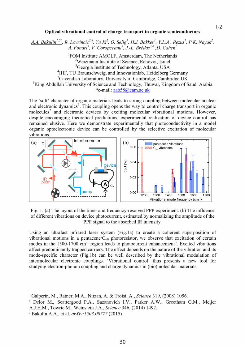
Optical vibrational control of charge transport in organic semiconductors
A.A. Bakulin1,5*, R. Lovrincic2,4, Yu Xi2, O. Selig1, H.J. Bakker1, Y.L.A . Rezus1, P.K. Nayak2,A. Fonari3, V. Coropceanu3, J.-L. Brédas3,6 ,D. Cahen2
1FOM Institute AMOLF, Amsterdam, The Netherlands2Weizmann Institute of Science, Rehovot, Israel3Georgia Institute of Technology, Atlanta, USA
4IHF, TU Braunschweig, and Innovationlab, Heidelberg Germany5Cavendish Laboratory, University of Cambridge, Cambridge UK
6King Abdullah University of Science and Technology, Thuwal, Kingdom of Saudi Arabia*e-mail: [email protected]
The ‘soft’ character of organic materials leads to strong coupling between molecular nuclear and electronic dynamics1. This coupling opens the way to control charge transport in organic molecules2 and electronic devices by exciting molecular vibrational motions. However, despite encouraging theoretical predictions, experimental realization of device control has remained elusive. Here we demonstrate experimentally that photoconductivity in a model organic optoelectronic device can be controlled by the selective excitation of molecular vibrations.
Fig. 1. (a) The layout of the time- and frequency-resolved PPP experiment. (b) The influence of different vibrations on device photocurrent, estimated by normalizing the amplitude of the
PPP signal to the absorbed IR intensity.
Using an ultrafast infrared laser system (Fig.1a) to create a coherent superposition of vibrational motions in a pentacene/C60 photoresistor, we observe that excitation of certain modes in the 1500-1700 cm-1 region leads to photocurrent enhancement3. Excited vibrations affect predominantly trapped carriers. The effect depends on the nature of the vibration and its mode-specific character (Fig.1b) can be well described by the vibrational modulation of intermolecular electronic couplings. ‘Vibrational control’ thus presents a new tool for studying electron-phonon coupling and charge dynamics in (bio)molecular materials.
1 Galperin, M., Ratner, M.A., Nitzan, A. & Troisi, A., Science 319, (2008) 1056.2 Delor M., Scattergood P.A., Sazanovich I.V., Parker A.W., Greetham G.M., Meijer A.J.H.M., Towrie M., Weinstein J.A., Science 346, (2014) 1492.3 Bakulin A.A., et al. arXiv:1503.00777 (2015)
(a) (b)
I-2

31
Optical vibrational control of charge transport in organic semiconductors
A.A. Bakulin1,5*, R. Lovrincic2,4, Yu Xi2, O. Selig1, H.J. Bakker1, Y.L.A . Rezus1, P.K. Nayak2,A. Fonari3, V. Coropceanu3, J.-L. Brédas3,6 ,D. Cahen2
1FOM Institute AMOLF, Amsterdam, The Netherlands2Weizmann Institute of Science, Rehovot, Israel3Georgia Institute of Technology, Atlanta, USA
4IHF, TU Braunschweig, and Innovationlab, Heidelberg Germany5Cavendish Laboratory, University of Cambridge, Cambridge UK
6King Abdullah University of Science and Technology, Thuwal, Kingdom of Saudi Arabia*e-mail: [email protected]
The ‘soft’ character of organic materials leads to strong coupling between molecular nuclear and electronic dynamics1. This coupling opens the way to control charge transport in organic molecules2 and electronic devices by exciting molecular vibrational motions. However, despite encouraging theoretical predictions, experimental realization of device control has remained elusive. Here we demonstrate experimentally that photoconductivity in a model organic optoelectronic device can be controlled by the selective excitation of molecular vibrations.
Fig. 1. (a) The layout of the time- and frequency-resolved PPP experiment. (b) The influence of different vibrations on device photocurrent, estimated by normalizing the amplitude of the
PPP signal to the absorbed IR intensity.
Using an ultrafast infrared laser system (Fig.1a) to create a coherent superposition of vibrational motions in a pentacene/C60 photoresistor, we observe that excitation of certain modes in the 1500-1700 cm-1 region leads to photocurrent enhancement3. Excited vibrations affect predominantly trapped carriers. The effect depends on the nature of the vibration and its mode-specific character (Fig.1b) can be well described by the vibrational modulation of intermolecular electronic couplings. ‘Vibrational control’ thus presents a new tool for studying electron-phonon coupling and charge dynamics in (bio)molecular materials.
1 Galperin, M., Ratner, M.A., Nitzan, A. & Troisi, A., Science 319, (2008) 1056.2 Delor M., Scattergood P.A., Sazanovich I.V., Parker A.W., Greetham G.M., Meijer A.J.H.M., Towrie M., Weinstein J.A., Science 346, (2014) 1492.3 Bakulin A.A., et al. arXiv:1503.00777 (2015)
(a) (b)
Resistive switch Red-Ox behavior as mechanism behind the operation of polyaniline memristors and neural network elements
D.Yu. Godovsky1, O. Bogomolova2, M. Kondratenko3, V. Sergeyev2
1 Institute of Elementoorganic Compounds RAS, Vavilova, 28, Moscow, 1999912 Moscow State University Chemistry Dept, Vorobievy Gory, Moscow, 199991
3 Moscow State University Physics Dept., Vorobievy Gory, Moscow, 199991
Memristors are becoming the real part of integral circuits and memory elements, though the mechanisms, governing their behavior are still under investigation and discussion. We studied polyaniline-based memristor films in solutions, using spectroelectrochemistry along with ACand DC conductivity measurements. The resistive switch effect mechanism was studied by us for polyaniline film memrisors in aqueous and non-aqueous solutions of H+ acids (HCl) and Li+-based salts (LiClO4 in acetonytrile). The spectroelectrochemical measurements were done along with cyclovotammetry and resistance measurements in AC and DC current mode of the films. We found, that the resistive switch (memristive) behavior can be explained by the change of Red-Ox states of PANI (Fig.1). The smooth and non threshold-like behavior of resistivity is due to the mixture of different red-ox states in different PANI segments (blocks)due to the local red-ox non-equality. This partwise, confirms the PANI structure model representing it as a co-polymer, having different types of segments (blocks) :dipheno-,benzene- . The retention of resistivity corresponding to the conservation of mentioned mixed Red-Ox states after switching-off the voltage observed both electrically and spectroelectrochemically, providing the basis for the memory effect of PANi memristors.Another key property of memristor – dependence of current state on the prehistory of charge injection/extraction at different voltages is also well explained, if assuming that different blocks (segments) in PANi can require different voltage or amount of charge for oxidation or reduction.
The behavior of PANi, where protons were substituted by Li+ ions in non-aqueous solutions of LiClO4 in acetonytrile show no conductivity threshold and no memristivebehavior either, which well corresponds to the Red-Ox chemistry of PANi in basic solutions. This points to the fact, that protons are necessary for the operation of PANi based memristors.The obtained results could shade light onto the basic principles of operation of inorganic memristors as well.
Also the possibility of PANi use for Artificial Neural Networks was opened, since PANi can make a conductive bridge (emeraldine salt) between two conductive contacts and stay in such position long time enough realizing Hebbian rule – two fired-two wired.
Fig.1 Different red-ox states of PANi, conductive one –emeraldine salt
I-3
32
Carbon nanomaterials for flexible and transparent electronics
A.G. Nasibulin 1,2
1 Department of Applied Physics, Aalto University School of Science, Puumiehenkuja 2, 00076, Espoo, Finland
2 Skolkovo Institute of Science and Technology, 100 Novaya st., Skolkovo, Odintsovsky district, Moscow Region, Russia 143025
*e-mail: [email protected]
Since the 1980s, carbon nanomaterials, such as fullerenes, nanofibers, carbon nanotubes, graphene, graphene nanoribbons, have attracted tremendous attention of the researchers due to their unique properties. In the presentation, different carbon nanomaterials, their properties and applications in flexible and transparent electronics will be reviewed. The main stress of the presentation will be on single-walled carbon nanotube films and graphene.
Carbon nanotubes (CNTs) are a unique family of materials exhibiting diverse useful chemical and physical properties. The CNTs and especially single-walled CNTs (SWCNTs) were found to have exceptional mechanical, thermal and electronic properties. Among different routes to synthesize SWCNTs, an aerosol CVD method is one of the most promising. This method allows growing high quality and clean SWCNTs with certain diameters and lengths.1 CNTs can be deposited onto practically any substrate, including temperature nontolerant polymers, so that time-consuming steps of CNT purification from the catalyst and support, dispersion and deposition processes are avoided. Taking into account high transparency, SWCNT films are a strong candidate for the replacement of commonly used transparent electrodes, such as indium-tin oxide (ITO), which have several drawbacks, including high refractive index and haze, spectrally non-uniform optical transmission, limited flexibility, restricted chemical robustness and depleted raw material supply. SWCNT networks have been demonstrated to show potential advantages in performance and fabrication cost reduction in comparison with ITO as well as most of organic materials that have been extensively studied as low-cost alternatives2. Furthermore, high flexibility of the SWCNTs opens avenues beyond the ITO, i.e. creation of completely new components, urgently needed in the flexible, transparent and stretchable electronics.3
Graphene possesses similar properties to SWCNTs. Graphene is strictly two-dimensional material exhibits exceptionally high crystal and electronic quality and, despite its short history, has already revealed a cornucopia of new physics and potential applications. It is tougher than diamond, but stretches like rubber. It is very transparent and conducts electricity and heat better than copper nanowires. The importance of graphene as a material for flexible optoelectronic applications is not in doubt including ITO replacement.
This work was partially supported by Ministry of Education and Science of Russian Federation (Project DOI: RFMEFI58114X0006).
1 Nasibulin, A. G., Shandakov, S. D., Zavodchikova, M., Kauppinen, E. I., Russian Chemical Review 80, 771-786 (2011). 2 Kaskela, A., Nasibulin, A.G., Zavodchikova, M., Aitchison, B., Papadimitratos, A., Tian, Y., Zhu, Z., Jiang, H., Brown, D.P., Zakhidov, A., and Kauppinen, E.I., Nano Letters 10, pp. 4349-4355 (2010).Nasibulin, A. G., Kaskela, A. O., Mustonen, K., Anisimov, A. S., Ruiz, V., Kivistö, S., Rackauskas, S., Timmermans, M. Y., Pudas, M., Aitchison, B., Kauppinen, M., Brown, D. P., Okhotnikov, O. G., Kauppinen, E. I., ACS Nano 5, 3214-3221 (2011).3 Sun, D-M., Timmermans, M.Y., Kaskela, A., Nasibulin, A.G., Kishimoto, S., Mizutani, T., Kauppinen, E.I., and Ohno, Y., Nature Communications 4, 2302 (2013).
I-4

33
Carbon nanomaterials for flexible and transparent electronics
A.G. Nasibulin 1,2
1 Department of Applied Physics, Aalto University School of Science, Puumiehenkuja 2, 00076, Espoo, Finland
2 Skolkovo Institute of Science and Technology, 100 Novaya st., Skolkovo, Odintsovsky district, Moscow Region, Russia 143025
*e-mail: [email protected]
Since the 1980s, carbon nanomaterials, such as fullerenes, nanofibers, carbon nanotubes, graphene, graphene nanoribbons, have attracted tremendous attention of the researchers due to their unique properties. In the presentation, different carbon nanomaterials, their properties and applications in flexible and transparent electronics will be reviewed. The main stress of the presentation will be on single-walled carbon nanotube films and graphene.
Carbon nanotubes (CNTs) are a unique family of materials exhibiting diverse useful chemical and physical properties. The CNTs and especially single-walled CNTs (SWCNTs) were found to have exceptional mechanical, thermal and electronic properties. Among different routes to synthesize SWCNTs, an aerosol CVD method is one of the most promising. This method allows growing high quality and clean SWCNTs with certain diameters and lengths.1 CNTs can be deposited onto practically any substrate, including temperature nontolerant polymers, so that time-consuming steps of CNT purification from the catalyst and support, dispersion and deposition processes are avoided. Taking into account high transparency, SWCNT films are a strong candidate for the replacement of commonly used transparent electrodes, such as indium-tin oxide (ITO), which have several drawbacks, including high refractive index and haze, spectrally non-uniform optical transmission, limited flexibility, restricted chemical robustness and depleted raw material supply. SWCNT networks have been demonstrated to show potential advantages in performance and fabrication cost reduction in comparison with ITO as well as most of organic materials that have been extensively studied as low-cost alternatives2. Furthermore, high flexibility of the SWCNTs opens avenues beyond the ITO, i.e. creation of completely new components, urgently needed in the flexible, transparent and stretchable electronics.3
Graphene possesses similar properties to SWCNTs. Graphene is strictly two-dimensional material exhibits exceptionally high crystal and electronic quality and, despite its short history, has already revealed a cornucopia of new physics and potential applications. It is tougher than diamond, but stretches like rubber. It is very transparent and conducts electricity and heat better than copper nanowires. The importance of graphene as a material for flexible optoelectronic applications is not in doubt including ITO replacement.
This work was partially supported by Ministry of Education and Science of Russian Federation (Project DOI: RFMEFI58114X0006).
1 Nasibulin, A. G., Shandakov, S. D., Zavodchikova, M., Kauppinen, E. I., Russian Chemical Review 80, 771-786 (2011). 2 Kaskela, A., Nasibulin, A.G., Zavodchikova, M., Aitchison, B., Papadimitratos, A., Tian, Y., Zhu, Z., Jiang, H., Brown, D.P., Zakhidov, A., and Kauppinen, E.I., Nano Letters 10, pp. 4349-4355 (2010).Nasibulin, A. G., Kaskela, A. O., Mustonen, K., Anisimov, A. S., Ruiz, V., Kivistö, S., Rackauskas, S., Timmermans, M. Y., Pudas, M., Aitchison, B., Kauppinen, M., Brown, D. P., Okhotnikov, O. G., Kauppinen, E. I., ACS Nano 5, 3214-3221 (2011).3 Sun, D-M., Timmermans, M.Y., Kaskela, A., Nasibulin, A.G., Kishimoto, S., Mizutani, T., Kauppinen, E.I., and Ohno, Y., Nature Communications 4, 2302 (2013).
Electronic properties of conjugated organic films and of their interfaces with solid surfaces studied by electron spectroscopy techniques.
A.S. KomolovSt. Petersburg state University
Electronic properties of the surfaces of the conjugated organic materials have attracted scientific interest because of possible applications in organic electronics devices as well as in single-molecule devices. The electron spectroscopy techniques were used successfully to characterize the energy level alignment and the density of the electronic states at organic film interfaces with metal and semiconductor surfaces. Selected results on the interfacial vacuum level shift and on the formation of a 5-7 nm extended interface layer obtained by core-level and ultraviolet photoelectron spectroscopy will be reviewed. The electronic properties of the surface organic layers can be tuned by means of the influence of the substrate material and by introducing polar substituents into the molecules. That may have a pronounced effect on the density of valence states and on the density of the unoccupied electronic states (DOS and DOUS, respectively). Particularly, the substitution by electron-withdrawing groups would typically provide a stabilization of the energy positions of the edges of the forbidden energy gap and to narrowing of the bandgap. The changes of the DOS peak structure can be monitored by means of ultraviolet photoelectron spectroscopy, the DOUS changes can be monitored by means of inverse photoemission spectroscopy (IPES), by means of near edge X-ray absorption spectroscopy (NEXAFS) and using the total current spectroscopy (TCS). The experimental results are supported by the results of the first-principle electron structure calculations. The recent results on the interface formation and on the DOUS of the ultrathin films of substituted fullerene and phthalocyanine films on solid surfaces are presented.
I-5

34
Toward a unified description of different intermolecular interactions in organic crystals. Combined X-ray Crystallographic, Infrared/Raman Spectroscopic and solid-state DFT
study.
M.V. VenerMendeleev University of Chemical Technology, Moscow, Russia
Kurnakov Institute of General and Inorganic Chemistry, RAS, Moscow, Russia
The enthalpy/energy Eint of a particular noncovalent/intermolecular interaction (NI) in solids is a target property in the context of crystal engineering, the theoretical prediction of high-performance novel organic semiconductor materials, the formation of pharmaceutical salts and cocrystals. In contract to the gas-phase species, a quantitative description of NIs in organic crystals is a difficult problem. To the experimental end, evaluation of the Eint value of the particular NI in a solid state requires the extraction of the cohesive energy per a considered interaction from the whole set of intermolecular interactions. Different energy decomposition schemes1,2 successfully used for the Eint computations in the gas-phase systems have a limited applicability for a solid state. The quantitative description of NIs in crystals can be reached by the Bader analysis of the periodic electron density in conjunction with the empirical formula relating the kinetic energy density at the bond critical point andEint
3,4. The key role in this approach plays solid-state DFT computations. The starting point is the X-ray data on the organic crystal structure (the cif file).
Several examples of the applicability of this approach to evaluation of different properties of one- and two component crystals will be given. (i) Theoretical IR spectrum in the 10 – 3600 frequency region of the serine-H2O and serine-H2O2 solvates5. (ii) Evaluation of the lattice energy of the pharmaceutical salts and cocrystals6,7. (iii) Applicability of the dimeric heterosynthon concept for the two-component crystals consisting of molecules with the equivalent binding sites8. (iv) Strength of hydrogen bonds in ionic liquids9.
1 B. Bankiewicz, P. Matczak, M. Palusiak, J. Phys. Chem. A 116 (2012) 452.2 M. Anand, I. Fernandez, H.F. Schaefer, et. al. J. Comput. Chem. 2015, DOI: 10.1002/jcc.23976.3 M.V. Vener, A.N. Egorova, A.V. Churakov, V.G. Tsirelson J. Comput. Chem. 33 (2012) 2303.4 A.V. Shishkina, V.V. Zhurov, A.I. Stash et al., Cryst. Growth Des. 13 (2013) 816.5 M. V. Vener, A. G. Medvedev, A. V. Churakov et al. J. Phys. Chem. A 115 (2011) 13657.6 A.N. Manin, A.P. Voronin, N.G. Manin et al. J. Phys. Chem. B 118 (2014) 6803.7 M. V. Vener, E. O. Levina, O. A. Koloskov, et al. Cryst. Growth Des. 14 (2014) 4997.8 A.G. Medvedev, A.V. Shishkina, P.V. Prikhodchenko et al. RSC Advances 5 (2015) 29601.9 S. A. Katsyuba, M. V. Vener, E. E. Zvereva et al. J. Phys. Chem. B 117 (2013) 9094.
I-6

35
Toward a unified description of different intermolecular interactions in organic crystals. Combined X-ray Crystallographic, Infrared/Raman Spectroscopic and solid-state DFT
study.
M.V. VenerMendeleev University of Chemical Technology, Moscow, Russia
Kurnakov Institute of General and Inorganic Chemistry, RAS, Moscow, Russia
The enthalpy/energy Eint of a particular noncovalent/intermolecular interaction (NI) in solids is a target property in the context of crystal engineering, the theoretical prediction of high-performance novel organic semiconductor materials, the formation of pharmaceutical salts and cocrystals. In contract to the gas-phase species, a quantitative description of NIs in organic crystals is a difficult problem. To the experimental end, evaluation of the Eint value of the particular NI in a solid state requires the extraction of the cohesive energy per a considered interaction from the whole set of intermolecular interactions. Different energy decomposition schemes1,2 successfully used for the Eint computations in the gas-phase systems have a limited applicability for a solid state. The quantitative description of NIs in crystals can be reached by the Bader analysis of the periodic electron density in conjunction with the empirical formula relating the kinetic energy density at the bond critical point andEint
3,4. The key role in this approach plays solid-state DFT computations. The starting point is the X-ray data on the organic crystal structure (the cif file).
Several examples of the applicability of this approach to evaluation of different properties of one- and two component crystals will be given. (i) Theoretical IR spectrum in the 10 – 3600 frequency region of the serine-H2O and serine-H2O2 solvates5. (ii) Evaluation of the lattice energy of the pharmaceutical salts and cocrystals6,7. (iii) Applicability of the dimeric heterosynthon concept for the two-component crystals consisting of molecules with the equivalent binding sites8. (iv) Strength of hydrogen bonds in ionic liquids9.
1 B. Bankiewicz, P. Matczak, M. Palusiak, J. Phys. Chem. A 116 (2012) 452.2 M. Anand, I. Fernandez, H.F. Schaefer, et. al. J. Comput. Chem. 2015, DOI: 10.1002/jcc.23976.3 M.V. Vener, A.N. Egorova, A.V. Churakov, V.G. Tsirelson J. Comput. Chem. 33 (2012) 2303.4 A.V. Shishkina, V.V. Zhurov, A.I. Stash et al., Cryst. Growth Des. 13 (2013) 816.5 M. V. Vener, A. G. Medvedev, A. V. Churakov et al. J. Phys. Chem. A 115 (2011) 13657.6 A.N. Manin, A.P. Voronin, N.G. Manin et al. J. Phys. Chem. B 118 (2014) 6803.7 M. V. Vener, E. O. Levina, O. A. Koloskov, et al. Cryst. Growth Des. 14 (2014) 4997.8 A.G. Medvedev, A.V. Shishkina, P.V. Prikhodchenko et al. RSC Advances 5 (2015) 29601.9 S. A. Katsyuba, M. V. Vener, E. E. Zvereva et al. J. Phys. Chem. B 117 (2013) 9094.
Computer simulation of microscopic ordering and charge transport in thiophene-based conjugated polymer PBTTT-C14
C. Poelking1, E. Cho2,3, A. Malafeev4, V. Ivanov4*, K. Kremer1, C. Risko2, J.-L. Brédas2,D. Andrienko1
1Max Planck Institute for Polymer Research, Mainz, Germany2School of Chemistry and Biochemistry and Center for Organic Photonics and Electronics,
Georgia Institute of Technology, Atlanta, Georgia, United States3School of Materials Science and Engineering, Georgia Institute of Technology, Atlanta,
Georgia, United States4Moscow State University, Faculty of Physics, Moscow, Russia
*e-mail: [email protected]
We have performed computer simulation study of the temperature dependence of the dynamic disorder in the crystalline lamellar arrangement of the highly crystalline conjugated polymer, poly(2,5-bis(3-tetradecylthiophen-2-yl)thieno[3,2-b]thiophene), PBTTT-C14, and established a link between the microscopic ordering and the charge-transport parameters. Thestructure disorder has been characterized by three order parameters: dynamic, nematic, and paracrystallinity. An abrupt decrease of the side-chain dynamic order, observed around 400 K, correlates well with a sharp increase of the backbone paracrystallinity, while all nematic and dynamic order parameters of the backbone as well as the unit-cell expansion along the π-stacking direction show a monotonic linear temperature dependence.
The morphological disorder leads to broadening of distributions of the electronic coupling elements and site energies. The variation in electronic couplings was found to occur on a much faster time scale (hundreds of femtoseconds) than a typical time required for a single electron-transfer event. Hence, the electronic coupling elements were preaveraged before calculating electron-transfer rates. Site energies, by contrast, were found to change on a significantly slower scale and thus could be treated as static on the time scale of charge transport. Finally, the hole mobility, reproduces well the value measured in a short-channel thin-film transistor. Preaveraging the electronic couplings (due to their fast dynamics) leads to a factor of 5 increase in the average mobility.
We came to the conclusion that, in order to secure polymeric organic semiconductors with large charge-carrier mobilities, it is not enough to have large electronic coupling averages. In addition, the fast time-scale dynamics of the polymers and, even more importantly, the small energetic disorder (which evolves on a much slower than the charge-carrier dynamics time scale) are desirable. From the point of view of chemical design, it should be noted that the alkyl side chains that are added for solubility purposes can affect the backbone paracrystallinity and hence increase the energetic disorder if they do not remain in a highly crystalline state. It is therefore important that both backbones and side chains maintain good crystalline order.
These results which will be presented at IFSOE-2015 have been published before1.
This work was partly supported by the DFG programs IRTG 1328 and SPP 1355, and BMBF grants MESOMERIE and MEDOS.
1 Poelking C., Cho E., Malafeev A., Ivanov V., Kremer K., Risko C., Brédas J.-L., Andrienko D. J. Phys. Chem. C 2013, 117, 1633−1640.
I-7

36
Charge transport in amorphous organic materials: effect of spatial correlation of the random energy landscape
S.V. NovikovA.N. Frumkin Institute of Physical Chemistry and Electrochemistry, Leninsky prosp. 31,
Moscow 119071, RussiaNational Research University Higher School of Economics, Myasnitskaya ul. 20, Moscow
101000, Russia
A general feature of amorphous organic materials is a long range spatial correlation of the random energy landscape U(r)1. Correlation arises because of the influence of themolecules having permanent dipole or quadrupole moments. For dipolar materials the energy correlation function has a form C(r) = ⟨U(r)U(0)⟩ ∝ 1/r, while for the quadrupolar materials C(r) ∝ 1/r3. Spatial correlations provide particular field dependence of the hopping carrier drift mobility µ(E) in organic materials2. Typically, in organic materials the density of states (DOS) has a Gaussian form. For the Gaussian DOS power law correlation function C(r) ∝1/rn gives the mobility field dependence lnµ(E) ∝ En/(n+1). This is the reason for the ubiquitous observation of the Poole-Frenkel mobility field dependence lnµ(E) ∝ E1/2 in amorphous organic materials1. Important property of the Gaussian DOS is the eventual development of the quasi-equilibrium (non-dispersive) transport regime for any temperature. In this regime the carrier mobility does not depend on time for t →∞.
Electrostatic origin of the random carrier energy in organic materials provides a non-trivial modification of the energy landscape at the vicinity of the conducting electrode. In the thing layer, relevant for injection, magnitude of the electrostatic disorder decays and correlation becomes different from the bulk. These variations lead to the much more uniform distribution of the injection current over electrode surface in organic electronic devices.
1 S.V. Novikov, A.V. Vannikov, J. Phys. Chem. C 113 (2009) 2532.2 S.V. Novikov, D.H. Dunlap, V.M. Kenkre, P.E. Parris, A.V. Vannikov, Phys. Rev. Lett. 81(1998) 4472.
I-8

37
Charge transport in amorphous organic materials: effect of spatial correlation of the random energy landscape
S.V. NovikovA.N. Frumkin Institute of Physical Chemistry and Electrochemistry, Leninsky prosp. 31,
Moscow 119071, RussiaNational Research University Higher School of Economics, Myasnitskaya ul. 20, Moscow
101000, Russia
A general feature of amorphous organic materials is a long range spatial correlation of the random energy landscape U(r)1. Correlation arises because of the influence of themolecules having permanent dipole or quadrupole moments. For dipolar materials the energy correlation function has a form C(r) = ⟨U(r)U(0)⟩ ∝ 1/r, while for the quadrupolar materials C(r) ∝ 1/r3. Spatial correlations provide particular field dependence of the hopping carrier drift mobility µ(E) in organic materials2. Typically, in organic materials the density of states (DOS) has a Gaussian form. For the Gaussian DOS power law correlation function C(r) ∝1/rn gives the mobility field dependence lnµ(E) ∝ En/(n+1). This is the reason for the ubiquitous observation of the Poole-Frenkel mobility field dependence lnµ(E) ∝ E1/2 in amorphous organic materials1. Important property of the Gaussian DOS is the eventual development of the quasi-equilibrium (non-dispersive) transport regime for any temperature. In this regime the carrier mobility does not depend on time for t →∞.
Electrostatic origin of the random carrier energy in organic materials provides a non-trivial modification of the energy landscape at the vicinity of the conducting electrode. In the thing layer, relevant for injection, magnitude of the electrostatic disorder decays and correlation becomes different from the bulk. These variations lead to the much more uniform distribution of the injection current over electrode surface in organic electronic devices.
1 S.V. Novikov, A.V. Vannikov, J. Phys. Chem. C 113 (2009) 2532.2 S.V. Novikov, D.H. Dunlap, V.M. Kenkre, P.E. Parris, A.V. Vannikov, Phys. Rev. Lett. 81(1998) 4472.
Organic electronics in Russia: current state and perspectivesD. Paraschuk
Faculty of Physics & International Laser Center, Lomonosov Moscow State University, Russia
The recent research on organic electronics in Russia is reviewed. The results of the most active Russian research groups are highlighted. The visibility of research on organic electronics in Russia at the international level is analyzed, active and possible collaborative international projects are considered. The results of the recent two IFSOE are summarized, and the IFSOE 2016 is discussed. Perspectives of organic electronics in Russia in education, research and industry are presented.
I-9

Oral talks

39
Fx-TCNQ family for systematic studies on organic single crystals
Y. Krupskaya1*, M. Gibertini2, N. Marzari2, A.F. Morpurgo1
1Department of Quantum Matter Physics (DQMP), University of Geneva2Theory and Simulation of Materials (THEOS), École Polytechnique Fédérale de Lausanne
*e-mail: [email protected]
It is believed that in the absence of extrinsic disorder, electronic transport in field effect transistors (FET) of top-quality organic molecular semiconductors occurs in the so-called band-like (intrinsic) regime, in which the carrier mobility increases upon lowering temperature. To access the intrinsic transport properties of organic FET it is essential to understand the nature of this regime and to identify the microscopic material parameters that favor its occurrence, which are both currently unknown. In this respect, comparative studies of different organic semiconductors are highly desired. It would be ideal to compare single crystals formed by identical constituent molecules, but having different crystal packing, resulting in different electronic bands and molecular motion and, therefore, different transport properties. However, such studies were not reported in organics due to the absence of suitable materials and because the number of organic molecular semiconductors known to exhibit band-like transport is very limited. We have shown experimentally that the Fx-TCNQ (fluorinated tetracyanoquinodimethane) molecules do constitute a suitable family for this kind of comparative studies1. Though these molecules are not identical, they are very similar: the only difference is that one or several H atoms in the TCNQ molecule are substituted by F atoms.
This work was enabled by a main, unanticipated finding. F2-TCNQ single-crystal FET reproducibly exhibit very high room-temperature electron mobility μ = 6-7 cm2V-1s-1,increasing by a factor of 3 to 4 upon reducing T from room temperature to 150 K, where it reaches a value μ = 25 cm2V-1s-1. These values represent the largest relative increase in mobility upon lowering T, ever reported in organic FET. This finding was unexpected, because TCNQ single-crystal FET were investigated earlier, and found to be of insufficient quality to access the band-like transport regime; similarly, our measurements on F4-TCNQ devices showed no sign of band-like transport. We performed X-ray analysis and atomic force microscopy (AFM) measurements to exclude a possibility of different quality of the crystals in the bulk and on the surface. There does not appear to be any obvious extrinsic reason to account for the observed large disparity in the transport properties of these three materials.To analyze the intrinsic properties of the three studied materials, and to understand why F2-TCNQ FET exhibit such an outstanding behavior, we have performed systematic structural studies and electronic band-structure calculations. We find that F2-TCNQ crystals have a crystalline structure with a primitive unit cell containing a single molecule, so that all the molecules in the crystal are oriented parallel to each other. Additionally, F2-TCNQ crystals have identical packing on two orthogonal crystals surfaces. We also find that the band originating from the overlap between LUMOs (lowest unoccupied molecular orbitals) has a very large width 0.8 eV (the largest among the organic molecular semiconductors commonly used for the realization of FET) and a clear three-dimensional character. All these properties are conducive to a more pronounced electron delocalization, which could account for the remarkable behavior of F2-TCNQ single-crystal FET.This work was supported by German Research Foundation DFG (project № KR 4364/1-1).
1 Y. Krupskaya, M. Gibertini, N. Marzari, A. F. Morpurgo. Adv. Mater. 2015, 27, 2453-2458.
O-1

40
Photoluminescent Kinetics in Crystalline Films of Thiophene-Phenylene Co-Oligomers
L.G. Kudryashova1*, V.A. Postnikov2, V.V. Bruevich1, O.V. Borshchev3, Yu.N. Luponosov3,S.A. Ponomarenko3, M.S. Pshenichnikov4, D.Yu. Paraschuk1
1Faculty of Physics and International Laser Center,Lomonosov Moscow State University, Russia
2Physics and Material Science Department, DNA CEA, Ukr.3 Institute of Synthetic Polymer Materials RAS, Russia
4 Zernike Institute for Advanced Materials University of Groningen, Netherlands*e-mail: [email protected]
Single crystals of thiophene-phenylene co-oligomers (TPCO) have already shown their high potential for organic optoelectronics as they combine efficient charge transport withhigh photoluminescence (PL) quantum yield (QY). However, the origin of this unique combination is yet unclear. Here we report on PL dynamics from novel TPCOs single crystals with the identical conjugated core (5,5’-diphenyl-2,2’-bithiophene, PTTP) and differentterminal substituents that have strong effect on the crystal packing. The PL QY from crystals is a factor of 2-3 higher than that in diluted solutions. The maximum QY exceeds 60% (re-absorption corrected) which is the highest among the insofar reported for the TPCOs. The single-exponential PL decay with a lifetime of ~1 ns is very close to the radiative lifetime which suggests low concentration of exciton traps. We also observed noticeable (especially at 77 K) spectral dynamics in the PL spectrum at ~100 ps time scale which are thought to indicate strong energy exchange between excitonic sub-ensembles in the TPCO crystals. This highlights extremely rich photophysics that could be harnessed in advanced organic light-emitting devices. This work was supported by RFBR (projects № 13-02-01313 and № 15-02-09375).
O-2

41
Photoluminescent Kinetics in Crystalline Films of Thiophene-Phenylene Co-Oligomers
L.G. Kudryashova1*, V.A. Postnikov2, V.V. Bruevich1, O.V. Borshchev3, Yu.N. Luponosov3,S.A. Ponomarenko3, M.S. Pshenichnikov4, D.Yu. Paraschuk1
1Faculty of Physics and International Laser Center,Lomonosov Moscow State University, Russia
2Physics and Material Science Department, DNA CEA, Ukr.3 Institute of Synthetic Polymer Materials RAS, Russia
4 Zernike Institute for Advanced Materials University of Groningen, Netherlands*e-mail: [email protected]
Single crystals of thiophene-phenylene co-oligomers (TPCO) have already shown their high potential for organic optoelectronics as they combine efficient charge transport withhigh photoluminescence (PL) quantum yield (QY). However, the origin of this unique combination is yet unclear. Here we report on PL dynamics from novel TPCOs single crystals with the identical conjugated core (5,5’-diphenyl-2,2’-bithiophene, PTTP) and differentterminal substituents that have strong effect on the crystal packing. The PL QY from crystals is a factor of 2-3 higher than that in diluted solutions. The maximum QY exceeds 60% (re-absorption corrected) which is the highest among the insofar reported for the TPCOs. The single-exponential PL decay with a lifetime of ~1 ns is very close to the radiative lifetime which suggests low concentration of exciton traps. We also observed noticeable (especially at 77 K) spectral dynamics in the PL spectrum at ~100 ps time scale which are thought to indicate strong energy exchange between excitonic sub-ensembles in the TPCO crystals. This highlights extremely rich photophysics that could be harnessed in advanced organic light-emitting devices. This work was supported by RFBR (projects № 13-02-01313 and № 15-02-09375).
Self-assembled monolayer field-effect transistors based on Langmuir films of organosilicon-containing of conjugated oligomers
A.S. Sizov1*, D.S. Anisimov1,2, E.V. Agina1, O.V. Borshchev1, S.N. Chvalun1, S.A. Ponomarenko1,3
1 Institute of Synthetic Polymer Materials RAS, Russia
2 Faculty of Physics & International Laser Center, Lomonosov Moscow State University, Russia
3Moscow State University, Department of Chemistry, Russia
*e-mail: [email protected]
Organic Field-Effect Transistor (OFET) is one of the main building blocks of low-cost polymer-based electronics. Monolayer OFETs is an object of growing scientific interest because of combination of moderate electrical performance and low semiconductor thickness, which makes them perspective in gas-sensing applications1. A traditional approach to the fabrication of monolayer OFETs is a self-assembly from the solution on the substrate. However, this process involves a formation of the covalent bonds between the semiconducting film and the dielectric. For this purpose self-assembly requires a chemically active molecules (e.g. chlorosilanes), which are not chemically stable in an air environment. In addition, the process of layer formation is relatively slow (tens of hours for full surface coverage).
Fig. 1. Transfer characteristics of the monolayer OFET (a) and morphology of O(Si-Und-4T-Hex)2 LB film studied with atomic force microscopy (b).
In this work, we apply the Langmuir-Blodgett (LB) and Langmuir-Schaefer (LS) techniques to the fabrication of self-assembled monolayer OFETs (SAMFETs) based on a series of functional and chemically inert conjugated oligomers. The electrical performance of such devices is typical for SAMFETs, the hole mobility is up to 3*10-3 cm2/Vs and the on-off ratio is up to 105 (Fig 1)2. The developed approach is relatively fast, environment-friendly and can be utilized in large-area low-cost electronics production. The fabricated devices are stable under air environment for at least 6 month, which makes them perspective as a basis for gas sensors. This work was supported by RFBR (grant 14-03-00873) and Russian Academy of Sciences (program OKh-3). 1 Andringa, A. M., Spijkman, M. J. et. al., Organic Electronics, 11, 895 (2010) 2 Sizov, A. S., Anisimov, D. S. at. al., Langmuir, 30, 15327 (2014)
a)
O-3
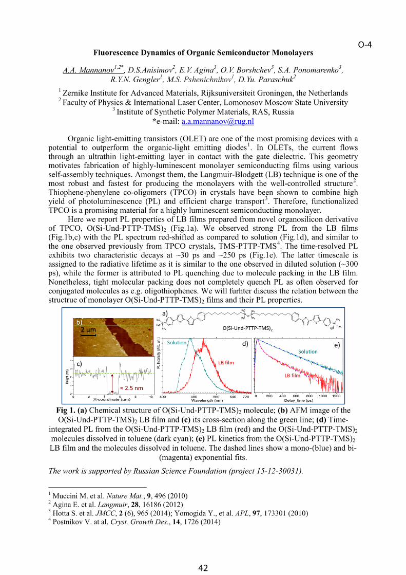
42
Fluorescence Dynamics of Organic Semiconductor Monolayers
A.A. Mannanov1,2*, D.S.Anisimov2, E.V. Agina3, O.V. Borshchev3, S.A. Ponomarenko3,R.Y.N. Gengler1, M.S. Pshenichnikov1, D.Yu. Paraschuk2
1 Zernike Institute for Advanced Materials, Rijksuniversiteit Groningen, the Netherlands2 Faculty of Physics & International Laser Center, Lomonosov Moscow State University
3 Institute of Synthetic Polymer Materials, RAS, Russia*e-mail: [email protected]
Organic light-emitting transistors (OLET) are one of the most promising devices with a potential to outperform the organic-light emitting diodes1. In OLETs, the current flows through an ultrathin light-emitting layer in contact with the gate dielectric. This geometry motivates fabrication of highly-luminescent monolayer semiconducting films using various self-assembly techniques. Amongst them, the Langmuir-Blodgett (LB) technique is one of the most robust and fastest for producing the monolayers with the well-controlled structure2.Thiophene-phenylene co-oligomers (TPCO) in crystals have been shown to combine high yield of photoluminescence (PL) and efficient charge transport3. Therefore, functionalized TPCO is a promising material for a highly luminescent semiconducting monolayer.
Here we report PL properties of LB films prepared from novel organosilicon derivative of TPCO, O(Si-Und-PTTP-TMS)2 (Fig.1a). We observed strong PL from the LB films (Fig.1b,c) with the PL spectrum red-shifted as compared to solution (Fig.1d), and similar to the one observed previously from TPCO crystals, TMS-PTTP-TMS4. The time-resolved PL exhibits two characteristic decays at ~30 ps and ~250 ps (Fig.1e). The latter timescale is assigned to the radiative lifetime as it is similar to the one observed in diluted solution (~300ps), while the former is attributed to PL quenching due to molecule packing in the LB film.Nonetheless, tight molecular packing does not completely quench PL as often observed for conjugated molecules as e.g. oligothiophenes. We will furhter discuss the relation between the structrue of monolayer O(Si-Und-PTTP-TMS)2 films and their PL properties.
Fig 1. (a) Chemical structure of O(Si-Und-PTTP-TMS)2 molecule; (b) AFM image of the O(Si-Und-PTTP-TMS)2 LB film and (c) its cross-section along the green line; (d) Time-
integrated PL from the O(Si-Und-PTTP-TMS)2 LB film (red) and the O(Si-Und-PTTP-TMS)2molecules dissolved in toluene (dark cyan); (e) PL kinetics from the O(Si-Und-PTTP-TMS)2LB film and the molecules dissolved in toluene. The dashed lines show a mono-(blue) and bi-
(magenta) exponential fits.
The work is supported by Russian Science Foundation (project 15-12-30031).
1 Muccini M. et al. Nature Mat., 9, 496 (2010)2 Agina E. et al. Langmuir, 28, 16186 (2012)3 Hotta S. et al. JMCC, 2 (6), 965 (2014); Yomogida Y., et al. APL, 97, 173301 (2010)4 Postnikov V. at al. Cryst. Growth Des., 14, 1726 (2014)
O-4
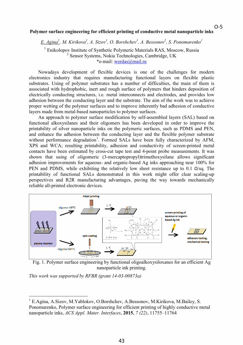
43
Fluorescence Dynamics of Organic Semiconductor Monolayers
A.A. Mannanov1,2*, D.S.Anisimov2, E.V. Agina3, O.V. Borshchev3, S.A. Ponomarenko3,R.Y.N. Gengler1, M.S. Pshenichnikov1, D.Yu. Paraschuk2
1 Zernike Institute for Advanced Materials, Rijksuniversiteit Groningen, the Netherlands2 Faculty of Physics & International Laser Center, Lomonosov Moscow State University
3 Institute of Synthetic Polymer Materials, RAS, Russia*e-mail: [email protected]
Organic light-emitting transistors (OLET) are one of the most promising devices with a potential to outperform the organic-light emitting diodes1. In OLETs, the current flows through an ultrathin light-emitting layer in contact with the gate dielectric. This geometry motivates fabrication of highly-luminescent monolayer semiconducting films using various self-assembly techniques. Amongst them, the Langmuir-Blodgett (LB) technique is one of the most robust and fastest for producing the monolayers with the well-controlled structure2.Thiophene-phenylene co-oligomers (TPCO) in crystals have been shown to combine high yield of photoluminescence (PL) and efficient charge transport3. Therefore, functionalized TPCO is a promising material for a highly luminescent semiconducting monolayer.
Here we report PL properties of LB films prepared from novel organosilicon derivative of TPCO, O(Si-Und-PTTP-TMS)2 (Fig.1a). We observed strong PL from the LB films (Fig.1b,c) with the PL spectrum red-shifted as compared to solution (Fig.1d), and similar to the one observed previously from TPCO crystals, TMS-PTTP-TMS4. The time-resolved PL exhibits two characteristic decays at ~30 ps and ~250 ps (Fig.1e). The latter timescale is assigned to the radiative lifetime as it is similar to the one observed in diluted solution (~300ps), while the former is attributed to PL quenching due to molecule packing in the LB film.Nonetheless, tight molecular packing does not completely quench PL as often observed for conjugated molecules as e.g. oligothiophenes. We will furhter discuss the relation between the structrue of monolayer O(Si-Und-PTTP-TMS)2 films and their PL properties.
Fig 1. (a) Chemical structure of O(Si-Und-PTTP-TMS)2 molecule; (b) AFM image of the O(Si-Und-PTTP-TMS)2 LB film and (c) its cross-section along the green line; (d) Time-
integrated PL from the O(Si-Und-PTTP-TMS)2 LB film (red) and the O(Si-Und-PTTP-TMS)2molecules dissolved in toluene (dark cyan); (e) PL kinetics from the O(Si-Und-PTTP-TMS)2LB film and the molecules dissolved in toluene. The dashed lines show a mono-(blue) and bi-
(magenta) exponential fits.
The work is supported by Russian Science Foundation (project 15-12-30031).
1 Muccini M. et al. Nature Mat., 9, 496 (2010)2 Agina E. et al. Langmuir, 28, 16186 (2012)3 Hotta S. et al. JMCC, 2 (6), 965 (2014); Yomogida Y., et al. APL, 97, 173301 (2010)4 Postnikov V. at al. Cryst. Growth Des., 14, 1726 (2014)
Polymer surface engineering for efficient printing of conductive metal nanoparticle inks
E. Agina1, M. Kirikova1, A. Sizov1, O. Borshchev1, A. Bessonov2, S. Ponomarenko1
1 Enikolopov Institute of Synthetic Polymeric Materials RAS, Moscow, Russia2 Sensor Systems, Nokia Technologies, Cambridge, UK
*e-mail: [email protected]
Nowadays development of flexible devices is one of the challenges for modern electronics industry that requires manufacturing functional layers on flexible plastic substrates. Using of polymer substrates has a number of difficulties, the main of them is associated with hydrophobic, inert and rough surface of polymers that hinders deposition of electrically conducting structures, i.e. metal interconnects and electrodes, and provides low adhesion between the conducting layer and the substrate. The aim of the work was to achieve proper wetting of the polymer surfaces and to improve inherently bad adhesion of conductive layers made from metal-based nanoparticles to polymer surfaces.
An approach to polymer surface modification by self-assembled layers (SAL) based onfunctional alkoxysilanes and their oligomers has been developed in order to improve the printability of silver nanoparticle inks on the polymeric surfaces, such as PDMS and PEN, and enhance the adhesion between the conducting layer and the flexible polymer substrate without performance degradation1. Formed SALs have been fully characterized by AFM, XPS and WCA; resulting printability, adhesion and conductivity of screen-printed metal contacts have been estimated by cross-cut tape test and 4-point probe measurements. It was shown that using of oligomeric (3-mercaptopropyl)trimethoxysilane allows significant adhesion improvements for aqueous- and organic-based Ag inks approaching near 100% for PEN and PDMS, while exhibiting the relatively low sheet resistance up to 0.1 Ω/sq. The printability of functional SALs demonstrated in this work might offer clear scaling-up perspectives and R2R manufacturing advantages, paving the way towards mechanically reliable all-printed electronic devices.
Fig. 1. Polymer surface engineering by functional oligoalkoxysiloxanes for an efficient Agnanoparticle ink printing.
This work was supported by RFBR (grant 14-03-00873a)
1 E.Agina, A.Sizov, M.Yablokov, O.Borshchev, A.Bessonov, M.Kirikova, M.Bailey, S. Ponomarenko, Polymer surface engineering for efficient printing of highly conductive metal nanoparticle inks, ACS Appl. Mater. Interfaces, 2015, 7 (22), 11755–11764
O-5

44
Determining the limiting factor for the organic solar efficiency with a new analytical kinetic model
A.Yu. Sosorev1, D.Yu. Godovsky2, D.Yu. Paraschuk1
1 Faculty of Physics and International Laser Center, M.V. Lomonosov Moscow State University,
2 Institute of Elementoorganic Compounds, Russian Academy of Science
Organic photovoltaics is a perspective alternative to the traditional inorganic solar cells due to the ease of production, lightweight and low cost. In the last decade, efficiency of the organic solar cells increased in several times approaching the lower limit of commercial viability. However, organic cells remain much less efficient than their inorganic counterparts. Nevertheless, ability to tune and improve properties of organic materials provides an opportunity for further increase of the organic solar cell performance. Theoretical modeling of the organic solar cell operation can yield an estimation of ultimate efficiency and provide a roadmap for further development.
In the present study, we suggest a new kinetic model of the organic solar cell operation. The model is based on the concept of two-step charge generation via intermediate charge-transfer (CT) states (Fig. 1). The first step, CT state formation, is described by Marcus model1, while the second step, CT state dissociation into free charges, is described by Onsager-Braun theory2 modified to account for the excess energy (“hotness”) of the states. In our modeling, excess energy is responsible for increased mobility of the non-thermalized charges generated upon CT state dissociation, in accordance with recent experimental findings3.
Within the frames of the suggested model, we address the impacts of the driving force, geminate recombination rate, charge mobility, average electron-hole separation in CT state, dielectric permittivity and reorganization energy on the organic solar cell efficiency, and conclude that the most important one is the reorganization energy. Interestingly, we find that when these properties are favorable, moderate variation in some of them results in insignificant variation of the cell efficiency. However, when these properties are poor, little variation of any of them significantly influences the cell performance. We address the ultimate efficiency in dependence of the bandgap and find that the model advices to use relatively large bandgaps (ca. 1.5-2 eV) as compared to that suggested by the Shockley-Quiesser model, until materials with significantly better electronic properties are found. We compare our findings with that of previously proposed models and discuss the physical reasons underlying the obtained results.
Fig. 1. Overview of the suggested model.
1 Marcus, R.A. Rev. Mod. Phys., 1993. 65(3): p. 599-610.2 Braun, C.L. J. Chem. Phys., 1984. 80(9): p. 4157-4161.3 Melianas, A., et al. Adv. Funct. Mater., 2014. 24(28): p. 4507-4514.
O-6
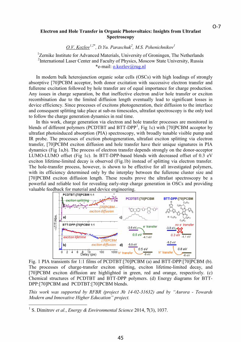
45
Determining the limiting factor for the organic solar efficiency with a new analytical kinetic model
A.Yu. Sosorev1, D.Yu. Godovsky2, D.Yu. Paraschuk1
1 Faculty of Physics and International Laser Center, M.V. Lomonosov Moscow State University,
2 Institute of Elementoorganic Compounds, Russian Academy of Science
Organic photovoltaics is a perspective alternative to the traditional inorganic solar cells due to the ease of production, lightweight and low cost. In the last decade, efficiency of the organic solar cells increased in several times approaching the lower limit of commercial viability. However, organic cells remain much less efficient than their inorganic counterparts. Nevertheless, ability to tune and improve properties of organic materials provides an opportunity for further increase of the organic solar cell performance. Theoretical modeling of the organic solar cell operation can yield an estimation of ultimate efficiency and provide a roadmap for further development.
In the present study, we suggest a new kinetic model of the organic solar cell operation. The model is based on the concept of two-step charge generation via intermediate charge-transfer (CT) states (Fig. 1). The first step, CT state formation, is described by Marcus model1, while the second step, CT state dissociation into free charges, is described by Onsager-Braun theory2 modified to account for the excess energy (“hotness”) of the states. In our modeling, excess energy is responsible for increased mobility of the non-thermalized charges generated upon CT state dissociation, in accordance with recent experimental findings3.
Within the frames of the suggested model, we address the impacts of the driving force, geminate recombination rate, charge mobility, average electron-hole separation in CT state, dielectric permittivity and reorganization energy on the organic solar cell efficiency, and conclude that the most important one is the reorganization energy. Interestingly, we find that when these properties are favorable, moderate variation in some of them results in insignificant variation of the cell efficiency. However, when these properties are poor, little variation of any of them significantly influences the cell performance. We address the ultimate efficiency in dependence of the bandgap and find that the model advices to use relatively large bandgaps (ca. 1.5-2 eV) as compared to that suggested by the Shockley-Quiesser model, until materials with significantly better electronic properties are found. We compare our findings with that of previously proposed models and discuss the physical reasons underlying the obtained results.
Fig. 1. Overview of the suggested model.
1 Marcus, R.A. Rev. Mod. Phys., 1993. 65(3): p. 599-610.2 Braun, C.L. J. Chem. Phys., 1984. 80(9): p. 4157-4161.3 Melianas, A., et al. Adv. Funct. Mater., 2014. 24(28): p. 4507-4514.
Electron and Hole Transfer in Organic Photovoltaics: Insights from Ultrafast Spectroscopy
O.V. Kozlov1,2*, D.Yu. Paraschuk2, M.S. Pshenichnikov1
1Zernike Institute for Advanced Materials, University of Groningen, The Netherlands2International Laser Center and Faculty of Physics, Moscow State University, Russia
*e-mail: [email protected]
In modern bulk heterojunction organic solar cells (OSCs) with high loadings of strongly absorptive [70]PCBM acceptor, both donor excitation with successive electron transfer and fullerene excitation followed by hole transfer are of equal importance for charge production.Any issues in charge separation, be that ineffective electron and/or hole transfer or exciton recombination due to the limited diffusion length eventually lead to significant losses in device efficiency. Since processes of excitons photogeneration, their diffusion to the interface and consequent splitting take place at sub-ns timescales, ultrafast spectroscopy is the only tool to follow the charge generation dynamics in real time.
In this work, charge generation via electron and hole transfer processes are monitored in blends of different polymers (PCDTBT and BTT-DPP1, Fig 1c) with [70]PCBM acceptor by ultrafast photoinduced absorption (PIA) spectroscopy, with broadly tunable visible pump and IR probe. The processes of exction photogeneration, ultrafast exciton splitting via electron transfer, [70]PCBM exciton diffusion and hole transfer have their unique signatures in PIA dynamics (Fig 1a,b). The process of electron transfer depends strongly on the donor-acceptor LUMO-LUMO offset (Fig 1c). In BTT-DPP-based blends with decreased offset of 0.3 eVexciton lifetime-limited decay is observed (Fig.1b) instead of splitting via electron transfer.The hole-transfer process, however, is shown to be effective for all investigated polymers, with its efficiency determined only by the interplay between the fullerene cluster size and [70]PCBM exciton diffusion length. These results prove the ultrafast spectroscopy be apowerful and reliable tool for revealing early-step charge generation in OSCs and providingvaluable feedback for material and device engineering.
Fig. 1 PIA transients for 1:1 films of PCDTBT:[70]PCBM (a) and BTT-DPP:[70]PCBM (b). The processes of charge-transfer exciton splitting, exciton lifetime-limited decay, and [70]PCBM exciton diffusion are highlighted in green, red and orange, respectively. (c) Chemical structures of PCDTBT and BTT-DPP polymers. (d) Energy diagrams for BTT-DPP:[70]PCBM and PCDTBT:[70]PCBM blends.This work was supported by RFBR (project № 14-02-31632) and by “Aurora - Towards Modern and Innovative Higher Education” project.
1 S. Dimitrov et al., Energy & Environmental Science 2014, 7(3), 1037.
O-7

46
Monte Carlo Simulations for Organic Materials
R. Volpi*, S. Stafström, M. LinaresDepartment of Physics, Chemistry and Biology, Linköping University
*email: [email protected]
In the last decades organic semiconductors, and in particular polymeric materials, have attracted a huge interest among scientists. They are low cost to produce and exhibit peculiar characteristics that can lead to new promising applications such as: organic light-emitting diodes (OLED) and organic solar cells (OPV). Theoretical studies are very useful for the improvement of such devices in terms of the understanding of their supramolecular organization and to help the polymer design process. The intrinsic probabilistic nature of the conduction, together with the structural disorder exhibited by these materials, render an analytical expression of the conductivity difficult; these aspects are instead suitable to be modeled in a Monte Carlo simulation1. In our previous study2 we focus on the mobility dependence of organic materials for a broad range of electric field strengths. It is well known in literature that to analyze this field dependence correctly, the spatial correlation effects in the energetic landscape have to be taken into account3,4. We propose a model suitable for an extended electric field range (0- 1.6x10⁷ V/cm). The mobility field dependence is not reducible to a single functional expression, such as Poole-Frenkel5, instead we have to take into account the existence of different operating regions, already known in literature. In particular we identify some important transition fields characteristic for every material that lead to the 3 important regions for the functional dependence of the mobility on the electric field: Percolation, Correlation and Inverted Marcus. In this way we are able to locate these 3 regions on the field axis. Monte-Carlo simulations of holes hopping in disordered PPV are presented and analyzed to support our thesis2.
Recents developments of our code including the presence of several charge carriers and the effects of polarization will be presented. These improvements are used for the studyof c60 material and of donor-acceptor interfaces.
1 M. Jakobsson, M. Linares, S. Stafström., J. Chem. Phys. 137, 114901 (2012)2 R. Volpi, S. Stafström, M. Linares. J. Chem. Phys. 142, 094503 (2015)3 D. Dunlap, V. Kenkre, P. Parris., J. Imag. Sci. and Tech. 43, 437 (1999)4 S. Novikov, A. Vannikov., J. Phys. Chem. 99, 14573 (1995)5 J. Frenkel., Phys. Rev. 54, 647 (1938).
Fig. 1: Traps analysis. Distribution of (a) dwell times and (b) hops numbers per molecule. Illustration of the system is presented in (c), the molecules are colored on the basis of the number of hops in a simulation. The scale is from red to blue, passing through white. In (d) we can see what we call a trapping resonant dimer, a composite trap that cannot be seen from the molecular dwell times distribution.
O-8

47
Monte Carlo Simulations for Organic Materials
R. Volpi*, S. Stafström, M. LinaresDepartment of Physics, Chemistry and Biology, Linköping University
*email: [email protected]
In the last decades organic semiconductors, and in particular polymeric materials, have attracted a huge interest among scientists. They are low cost to produce and exhibit peculiar characteristics that can lead to new promising applications such as: organic light-emitting diodes (OLED) and organic solar cells (OPV). Theoretical studies are very useful for the improvement of such devices in terms of the understanding of their supramolecular organization and to help the polymer design process. The intrinsic probabilistic nature of the conduction, together with the structural disorder exhibited by these materials, render an analytical expression of the conductivity difficult; these aspects are instead suitable to be modeled in a Monte Carlo simulation1. In our previous study2 we focus on the mobility dependence of organic materials for a broad range of electric field strengths. It is well known in literature that to analyze this field dependence correctly, the spatial correlation effects in the energetic landscape have to be taken into account3,4. We propose a model suitable for an extended electric field range (0- 1.6x10⁷ V/cm). The mobility field dependence is not reducible to a single functional expression, such as Poole-Frenkel5, instead we have to take into account the existence of different operating regions, already known in literature. In particular we identify some important transition fields characteristic for every material that lead to the 3 important regions for the functional dependence of the mobility on the electric field: Percolation, Correlation and Inverted Marcus. In this way we are able to locate these 3 regions on the field axis. Monte-Carlo simulations of holes hopping in disordered PPV are presented and analyzed to support our thesis2.
Recents developments of our code including the presence of several charge carriers and the effects of polarization will be presented. These improvements are used for the studyof c60 material and of donor-acceptor interfaces.
1 M. Jakobsson, M. Linares, S. Stafström., J. Chem. Phys. 137, 114901 (2012)2 R. Volpi, S. Stafström, M. Linares. J. Chem. Phys. 142, 094503 (2015)3 D. Dunlap, V. Kenkre, P. Parris., J. Imag. Sci. and Tech. 43, 437 (1999)4 S. Novikov, A. Vannikov., J. Phys. Chem. 99, 14573 (1995)5 J. Frenkel., Phys. Rev. 54, 647 (1938).
Fig. 1: Traps analysis. Distribution of (a) dwell times and (b) hops numbers per molecule. Illustration of the system is presented in (c), the molecules are colored on the basis of the number of hops in a simulation. The scale is from red to blue, passing through white. In (d) we can see what we call a trapping resonant dimer, a composite trap that cannot be seen from the molecular dwell times distribution.
Dielectric Effects at Organic/Inorganic Interfaces in Nanostructured Devices
T.S. Sherkar1*, L.J.A. Koster1
1Photophysics and Optoelectronics, Zernike Institute for Advanced Materials*e-mail: [email protected]
Dielectric interfaces are universal in organic electronic devices and are central to the device performance as they are active sites for generation and recombination of charge carriers. The hypotheses for charge carrier recombination include the pinning down of the charge carrier at the interface via coulomb interaction as a result of the mismatch (ε2/ε1) in the dielectric constant (ε) of the materials forming the interface1,2. Electrostatic polarization in presence of the dielectric mismatch is known to give rise to induced surface charges on the interface. Here, we embark on a theoretical approach to understand the electrostatic effects due to induced charges on interfaces which are known to influence the local charge dynamics during device operation.
Due to the high mismatch in the dielectric constant between materials used in hybrid organic/inorganic (OI) devices, these systems serve as an ideal platform to study the modified electrostatic effects due to the presence of a dielectric interface.
We consider a charge separation scenario across the interface and calculate the binding energy of the charge carrier for variations in the interfacial factors as described below. We find that the high dielectric mismatch (ε2/ε1 > 10) is responsible for binding of the charge carrier with energies above several kT. For the variation in interface shape and size (both defined by the morphology), we show that assumption of the planar interface (infinitely long) overestimates the attractive potential. The change in the interface curvature (defined by the local shape and size) affects the binding energy of the charge carrier by order of kT.Anisotropy is shown to critically affect the electrostatic force along the principal axis, while the binding energy of the charge is altered by more than 5 kT.
We are able to give an upper limit on the change in the binding energy for the variations in the above interfacial factors. These limits can serve as guidelines for optimization, interface engineering and design of high efficiency organic electronics devices.
1 Graetzel, M.; Janssen, R. a J.; Mitzi, D. B.; Sargent, E. H. Nature 2012, 488, 304–312.2 Noone, K. M.; Subramaniyan, S.; Zhang, Q.; Cao, G.; Jenekhe, S. A.; Ginger, D. S. J. Phys.Chem. C 2011, 115, 24403–24410.
Fig.1. Dielectric mismatch in hybrid organic/inorganic devices results in pinning of hole to the interface with binding energy in the order of several kT. This scenario is unfavorable for efficient charge separation and transport.
O-9

48
Effective Temperature and Universal Conductivity Scaling in Organic Semiconductors
H. Abdalla1*, K. Van de Ruit2 ,M. Kemerink1,2
1 Department of Physics, Chemistry and Biology, Linköping University, Sweden2 Eindhoven University of Technology, Department of Applied Physics, The Netherlands
*e-mail: [email protected]
For many disordered organic semiconductors with high charge carrier concentrations the conductivity has been found to show power-law temperature dependence in the Ohmic regime and a steeper power-law dependence on the field in the non-Ohmic regime. If the current is scaled as 𝑗𝑗𝑗𝑗 𝑇𝑇𝑇𝑇1+𝛼𝛼𝛼𝛼⁄ vs. 𝑉𝑉𝑉𝑉 𝑇𝑇𝑇𝑇⁄ , as in Fig.1, a single universal line is obtained. This concept is commonly referred to as Universal Scaling (US). Several theoretical frameworks based on fundamentally different and mutually exclusive physical mechanisms exist that attempt to derive or explain US. However, no consensus has been reached.
0.01 0.1 1 10 100 100010-5
10-4
10-3
10-2
10-1
100
101
102
1030.01 0.1 1 10 100 1000
10-5
10-4
10-3
10-2
10-1
100
101
102
103
J/T(1
+α) (A
/m2 K
α+1
)
eV/kT
4.00034.0064.0094.00124.0154.0184.0214.0244.0274.0304.0
Fig. 1. Collapse of all current data of measurements of PEDOT:PSS at different temperatures and electric fields to one universal line with two distinct regimes, Ohmic and non-Ohmic, as
indicated by the dotted lines
Universal curves can also be obtained using a seemingly unrelated procedure, first described by Marianer and Shklovskii (MS) for an exponential DOS, and later extended to Gaussian DOS.. This effective temperature (𝑇𝑇𝑇𝑇𝑒𝑒𝑒𝑒𝑒𝑒𝑒𝑒𝑒𝑒𝑒𝑒) concept states that the field has a similar effect on carrier transport as the lattice temperature and that the effect of both can be combined into 𝑇𝑇𝑇𝑇𝑒𝑒𝑒𝑒𝑒𝑒𝑒𝑒𝑒𝑒𝑒𝑒 . Plotting 𝑇𝑇𝑇𝑇𝑒𝑒𝑒𝑒𝑒𝑒𝑒𝑒𝑒𝑒𝑒𝑒 𝑇𝑇𝑇𝑇⁄ vs. 𝑞𝑞𝑞𝑞𝑞𝑞𝑞𝑞𝑞𝑞𝑞𝑞 𝑘𝑘𝑘𝑘𝐵𝐵𝐵𝐵𝑇𝑇𝑇𝑇⁄ collapses all data points to a single universal line.Here we show that US and MS are equally applicable to an extensive dataset on PEDOT:PSS and in fact exhibit full functional equivalency in field and temperature dependence. Furthermore, we show by means of kinetic Monte Carlo (kMC) simulations that both concepts have their physical origin in the heating of the charge carrier distribution. Due to the time-dependent nature of kMC we were able to study the energy relaxation of the charge carriers and to derive an analytical model based on a simple heat balance that consistently describes US and MS-type behavior.
O-10

49
Effective Temperature and Universal Conductivity Scaling in Organic Semiconductors
H. Abdalla1*, K. Van de Ruit2 ,M. Kemerink1,2
1 Department of Physics, Chemistry and Biology, Linköping University, Sweden2 Eindhoven University of Technology, Department of Applied Physics, The Netherlands
*e-mail: [email protected]
For many disordered organic semiconductors with high charge carrier concentrations the conductivity has been found to show power-law temperature dependence in the Ohmic regime and a steeper power-law dependence on the field in the non-Ohmic regime. If the current is scaled as 𝑗𝑗𝑗𝑗 𝑇𝑇𝑇𝑇1+𝛼𝛼𝛼𝛼⁄ vs. 𝑉𝑉𝑉𝑉 𝑇𝑇𝑇𝑇⁄ , as in Fig.1, a single universal line is obtained. This concept is commonly referred to as Universal Scaling (US). Several theoretical frameworks based on fundamentally different and mutually exclusive physical mechanisms exist that attempt to derive or explain US. However, no consensus has been reached.
0.01 0.1 1 10 100 100010-5
10-4
10-3
10-2
10-1
100
101
102
1030.01 0.1 1 10 100 1000
10-5
10-4
10-3
10-2
10-1
100
101
102
103
J/T(1
+α) (A
/m2 K
α+1
)
eV/kT
4.00034.0064.0094.00124.0154.0184.0214.0244.0274.0304.0
Fig. 1. Collapse of all current data of measurements of PEDOT:PSS at different temperatures and electric fields to one universal line with two distinct regimes, Ohmic and non-Ohmic, as
indicated by the dotted lines
Universal curves can also be obtained using a seemingly unrelated procedure, first described by Marianer and Shklovskii (MS) for an exponential DOS, and later extended to Gaussian DOS.. This effective temperature (𝑇𝑇𝑇𝑇𝑒𝑒𝑒𝑒𝑒𝑒𝑒𝑒𝑒𝑒𝑒𝑒) concept states that the field has a similar effect on carrier transport as the lattice temperature and that the effect of both can be combined into 𝑇𝑇𝑇𝑇𝑒𝑒𝑒𝑒𝑒𝑒𝑒𝑒𝑒𝑒𝑒𝑒 . Plotting 𝑇𝑇𝑇𝑇𝑒𝑒𝑒𝑒𝑒𝑒𝑒𝑒𝑒𝑒𝑒𝑒 𝑇𝑇𝑇𝑇⁄ vs. 𝑞𝑞𝑞𝑞𝑞𝑞𝑞𝑞𝑞𝑞𝑞𝑞 𝑘𝑘𝑘𝑘𝐵𝐵𝐵𝐵𝑇𝑇𝑇𝑇⁄ collapses all data points to a single universal line.Here we show that US and MS are equally applicable to an extensive dataset on PEDOT:PSS and in fact exhibit full functional equivalency in field and temperature dependence. Furthermore, we show by means of kinetic Monte Carlo (kMC) simulations that both concepts have their physical origin in the heating of the charge carrier distribution. Due to the time-dependent nature of kMC we were able to study the energy relaxation of the charge carriers and to derive an analytical model based on a simple heat balance that consistently describes US and MS-type behavior.
Understanding diffusion of charged, singlet and triplet excitations in disordered organic semiconductors
S. Athanasopoulos1*, S.T. Hoffmann1, I.I. Fishchuk2, A. Kadashchuk2, H. Bässler1, A. Köhler1
1Experimental Physics II, University of Bayreuth2Institute for Nuclear Research, National Academy of Sciences of Ukraine
*e-mail: [email protected]
The transport of charges and neutral excitations in disordered molecular systems triggers significant electronic processes that govern the efficiency of organic semiconductor devices. For example, in polymer-fullerene organic solar cells light absorption creates spin-singlet excitons that should reach by diffusion to an interface between the donor and acceptor material in order to dissociate to free carriers. Subsequently these carriers have to find their way to the electrodes by avoiding recombination in order to contribute to the photocurrent. Similarly, the transport of triplet states plays an important role in hybrid organic-inorganic solar cells that utilise the fission of a photogenerated singlet exciton to two triplet excitons in order to achieve conversion efficiencies that overome the Shockley-Queisser limit. In OLEDs both triplet and singlet excitons are generated by the recombination of electron and hole charges injected from the electrodes. The emission of these species and their up-converted or down-converted products will determine the efficiency and colour of the display.
Here we investigate how electronic excitations, namely charges, singlet and triplet excitons, diffuse by hopping in disordered organic materials with an aim to obtain a unified description of their transport properties. We pinpoint important similarities but also crucial differences on their transport characteristics. For this, we have combined luminescence experiments for a representative range of polymers and oligomers having various degrees of conjugation with Monte Carlo transport simulations to describe temperature dependent diffusion of excitations that couple by short- or long-range interactions in both equilibrium and at non-equilibrium conditions1. We find that below a disorder controlled transition temperature, transport of triplets/charges most often becomes kinetically frustrated in contrast to transport of singlets. However, by modelling the spectral relaxation we show that the appearance of frustrated diffusion is not intrinsically linked to the type of excitation or the transfer mechanism but is rather a fingerprint of the available target sites2. Monte Carlo simulations are in agreement with analytical theory at the limits of zero and room temperature and a scaling of the diffusivity and the spectral shift with the dimensionless disorder parameter is obtained for all types of excitations. Finally we compare polaronic versus disorder hopping transport for charge carriers and triplet excitons and determine under which conditions each transport regime is met. A recently developed analytical model3 sheds light on the gap between disorder and polaron controlled transport formulations.
1 Hoffmann S.T., Athanasopoulos S., Beljonne D., Bässler H., Köhler A. J. Phys. Chem. C2012, 116, 16371-16383, “How do Triplets and Charges Move in Disordered Organic Semiconductors? A Monte Carlo Study Comprising the Equilibrium and Nonequilibrium Regime”.2 Athanasopoulos S., Hoffmann S.T., Bässler H., Köhler A., Beljonne D. J. Phys. Chem. Lett.2013, 4, 1694-1700, “To Hop or Not to Hop? Understanding the Temperature Dependence of Spectral Diffusion in Organic Semiconductors”.3 Fishchuk I.I., Kadashchuk A., Hoffmann S.T., Athanasopoulos S., Genoe J., Bässler H., Köhler A. Phys. Rev. B 2013, 88, 125202, “Unified Description for Hopping Transport in Organic Semiconductors Including Both Energetic Disorder and Polaronic Contributions”
O-11

50
Low-temperature transport properties of long lived photo-excitations in organic materials
A.D. Chepelianskii1,2*, S.L. Bayliss2, H. Bouchiat1, N.C. Geenham2, R.H. Friend3
1LPS, Univ. Paris-Sud, CNRS UMR 8502, F-91405, Orsay, France 2Cavendish Laboratory, University of Cambridge, Cambridge, CB3 OHE, U.K
*e-mail: [email protected]
In organic semi-conductors long lived photo-induced excitations can take the form of electron-hole pairs and triplet excitons which are respectively protected by charge and spin conservation. We determined the localization length of the photo-induced charges in a photovoltaic donor-acceptor blend at low temperatures by comparing their dielectric and electron spin-resonance susceptibilities. Our results show that at cryogenic temperatures excitons are dissociated into long lived states, but that these are confined within a separation of around 4nm. We also measured the Debye and recombination times, showing the coexistence of a fast electrical response corresponding to delocalized motion, with glass-like recombination kinetics.
We then investigated spin dependentrecombination pathways for triplet excitons generated by singlet fission using optically detected magnetic resonance. We showed that geminate recombination between a pair of triplets in TIPS-tetracene and non-geminate triplet-triplet annihilation are characterized by distinct magnetic resonance line-shapes at low temperatures.
_______________________ 1 A.D. Chepelianskii, Jianpu Wang, R.H. Friend, Phys. Rev. Lett. 112, 126802 (2014)2 S.L. Bayliss, A.D. Chepelianskii, A. Sepe, B.J. Walker, B. Ehrler, M.J. Bruzek, J.E. Anthony and N.C. Greenham, Phys. Rev. Lett. 112, 238701 (2014).
Figure 1. Schematic of the experiment: Nb meanders forming asuperconducting resonator are covered by a thin PV layer. The sample can be excited both optically and by AC electric and magnetic fields created by within the resonator. A scanning electron microscope image of the resonator is shown on top-right inset, and the chemical formulas of the studied molecules are shown on the right.
O-12

51
Low-temperature transport properties of long lived photo-excitations in organic materials
A.D. Chepelianskii1,2*, S.L. Bayliss2, H. Bouchiat1, N.C. Geenham2, R.H. Friend3
1LPS, Univ. Paris-Sud, CNRS UMR 8502, F-91405, Orsay, France 2Cavendish Laboratory, University of Cambridge, Cambridge, CB3 OHE, U.K
*e-mail: [email protected]
In organic semi-conductors long lived photo-induced excitations can take the form of electron-hole pairs and triplet excitons which are respectively protected by charge and spin conservation. We determined the localization length of the photo-induced charges in a photovoltaic donor-acceptor blend at low temperatures by comparing their dielectric and electron spin-resonance susceptibilities. Our results show that at cryogenic temperatures excitons are dissociated into long lived states, but that these are confined within a separation of around 4nm. We also measured the Debye and recombination times, showing the coexistence of a fast electrical response corresponding to delocalized motion, with glass-like recombination kinetics.
We then investigated spin dependentrecombination pathways for triplet excitons generated by singlet fission using optically detected magnetic resonance. We showed that geminate recombination between a pair of triplets in TIPS-tetracene and non-geminate triplet-triplet annihilation are characterized by distinct magnetic resonance line-shapes at low temperatures.
_______________________ 1 A.D. Chepelianskii, Jianpu Wang, R.H. Friend, Phys. Rev. Lett. 112, 126802 (2014)2 S.L. Bayliss, A.D. Chepelianskii, A. Sepe, B.J. Walker, B. Ehrler, M.J. Bruzek, J.E. Anthony and N.C. Greenham, Phys. Rev. Lett. 112, 238701 (2014).
Figure 1. Schematic of the experiment: Nb meanders forming asuperconducting resonator are covered by a thin PV layer. The sample can be excited both optically and by AC electric and magnetic fields created by within the resonator. A scanning electron microscope image of the resonator is shown on top-right inset, and the chemical formulas of the studied molecules are shown on the right.
Open circuit voltage and efficiency in ternary OPV blends
N. Felekidis1*, E. Wang2, M. Kemerink1,3**1 Complex Materials and Devices, Department of Physics, Chemistry and Biology, Linköping
University2 Department of Chemistry and Chemical Engineering, Chalmers University of Technology
3 Department of Applied Physics, Eindhoven University of Technology*e-mail: [email protected]**e-mail: [email protected]
The tunability of the open-circuit voltage (Voc) in ternary blend bulk heterojunction (BHJ) solar cells has been demonstrated for a large number of material systems.1,2,3 Rather than being pinned by the lowest effective bandgap, Voc is -surprisingly- found to be a smooth function of the ratio of the two donor polymers or the two acceptor fullerenes. Combining experiments and modeling we arrive at a simple physical understanding of the composition dependence of Voc in ternary BHJ. This insight is subsequently used to assess the potential efficiency increase in these systems. We consistently find that for given Donor1, 2 energy levels, systematic but modest efficiency improvements can be reached in ternary systems as compared to binary ones. However, for state-of-the-art absorbers, having broad and strong absorption bands, and (close to) ideal energy levels, we find that ternary blends offer no advantages over binary ones.
Figure 1. Plot of Voc of ternary organic BHJ vs. donor ratio; binary compounds sit at 0 and 1. Symbols and lines are experimental data and model results for the indicated two-donor-single
acceptor systems.
1 Luyao Lu, Tao Xu, Wei Chen, Erik S. Landry, Luping Yu, Ternary blend polymer solar cells with enhanced power conversion efficiency, Nature Photonics, September 20142 Petr P. Khlyabich, Beate Burkhart, Barry C. Thompson, Compositional Dependence of the Open-Circuit Voltage in Ternary Blend Bulk Heterojunction Solar Cells Based on Two Donor Polymers, Journal of the American Chemical Society, 15 May 20123 Petr P. Khlyabich, Beate Burkhart, Barry C. Thompson, Efficient Ternary Blend Bulk Heterojunction Solar Cells with Tunable Open-Circuit Voltage, American Chemical Society,2011
O-13
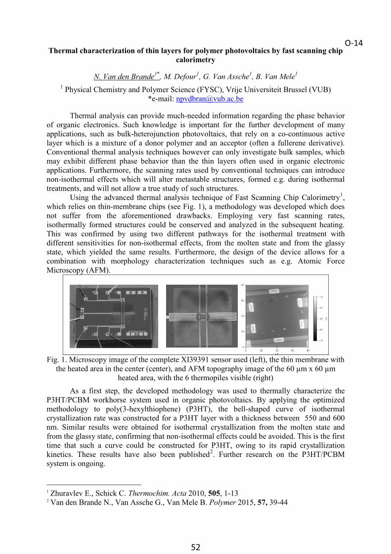
52
Thermal characterization of thin layers for polymer photovoltaics by fast scanning chip calorimetry
N. Van den Brande1*, M. Defour1, G. Van Assche1, B. Van Mele1
1 Physical Chemistry and Polymer Science (FYSC), Vrije Universiteit Brussel (VUB)*e-mail: [email protected]
Thermal analysis can provide much-needed information regarding the phase behavior of organic electronics. Such knowledge is important for the further development of many applications, such as bulk-heterojunction photovoltaics, that rely on a co-continuous active layer which is a mixture of a donor polymer and an acceptor (often a fullerene derivative). Conventional thermal analysis techniques however can only investigate bulk samples, which may exhibit different phase behavior than the thin layers often used in organic electronic applications. Furthermore, the scanning rates used by conventional techniques can introduce non-isothermal effects which will alter metastable structures, formed e.g. during isothermal treatments, and will not allow a true study of such structures.
Using the advanced thermal analysis technique of Fast Scanning Chip Calorimetry1,which relies on thin-membrane chips (see Fig. 1), a methodology was developed which does not suffer from the aforementioned drawbacks. Employing very fast scanning rates, isothermally formed structures could be conserved and analyzed in the subsequent heating. This was confirmed by using two different pathways for the isothermal treatment with different sensitivities for non-isothermal effects, from the molten state and from the glassy state, which yielded the same results. Furthermore, the design of the device allows for acombination with morphology characterization techniques such as e.g. Atomic ForceMicroscopy (AFM).
Fig. 1. Microscopy image of the complete XI39391 sensor used (left), the thin membrane with the heated area in the center (center), and AFM topography image of the 60 µm x 60 µm
heated area, with the 6 thermopiles visible (right)As a first step, the developed methodology was used to thermally characterize the
P3HT/PCBM workhorse system used in organic photovoltaics. By applying the optimized methodology to poly(3-hexylthiophene) (P3HT), the bell-shaped curve of isothermal crystallization rate was constructed for a P3HT layer with a thickness between 550 and 600nm. Similar results were obtained for isothermal crystallization from the molten state andfrom the glassy state, confirming that non-isothermal effects could be avoided. This is the first time that such a curve could be constructed for P3HT, owing to its rapid crystallization kinetics. These results have also been published2. Further research on the P3HT/PCBM system is ongoing.
1 Zhuravlev E., Schick C. Thermochim. Acta 2010, 505, 1-132 Van den Brande N., Van Assche G., Van Mele B. Polymer 2015, 57, 39-44
O-14
53
Thermal characterization of thin layers for polymer photovoltaics by fast scanning chip calorimetry
N. Van den Brande1*, M. Defour1, G. Van Assche1, B. Van Mele1
1 Physical Chemistry and Polymer Science (FYSC), Vrije Universiteit Brussel (VUB)*e-mail: [email protected]
Thermal analysis can provide much-needed information regarding the phase behavior of organic electronics. Such knowledge is important for the further development of many applications, such as bulk-heterojunction photovoltaics, that rely on a co-continuous active layer which is a mixture of a donor polymer and an acceptor (often a fullerene derivative). Conventional thermal analysis techniques however can only investigate bulk samples, which may exhibit different phase behavior than the thin layers often used in organic electronic applications. Furthermore, the scanning rates used by conventional techniques can introduce non-isothermal effects which will alter metastable structures, formed e.g. during isothermal treatments, and will not allow a true study of such structures.
Using the advanced thermal analysis technique of Fast Scanning Chip Calorimetry1,which relies on thin-membrane chips (see Fig. 1), a methodology was developed which does not suffer from the aforementioned drawbacks. Employing very fast scanning rates, isothermally formed structures could be conserved and analyzed in the subsequent heating. This was confirmed by using two different pathways for the isothermal treatment with different sensitivities for non-isothermal effects, from the molten state and from the glassy state, which yielded the same results. Furthermore, the design of the device allows for acombination with morphology characterization techniques such as e.g. Atomic ForceMicroscopy (AFM).
Fig. 1. Microscopy image of the complete XI39391 sensor used (left), the thin membrane with the heated area in the center (center), and AFM topography image of the 60 µm x 60 µm
heated area, with the 6 thermopiles visible (right)As a first step, the developed methodology was used to thermally characterize the
P3HT/PCBM workhorse system used in organic photovoltaics. By applying the optimized methodology to poly(3-hexylthiophene) (P3HT), the bell-shaped curve of isothermal crystallization rate was constructed for a P3HT layer with a thickness between 550 and 600nm. Similar results were obtained for isothermal crystallization from the molten state andfrom the glassy state, confirming that non-isothermal effects could be avoided. This is the first time that such a curve could be constructed for P3HT, owing to its rapid crystallization kinetics. These results have also been published2. Further research on the P3HT/PCBM system is ongoing.
1 Zhuravlev E., Schick C. Thermochim. Acta 2010, 505, 1-132 Van den Brande N., Van Assche G., Van Mele B. Polymer 2015, 57, 39-44
New methodology based on fast scanning calorimetry to determine the eutectic composition of polymer/fullerene organic photovoltaics.
M. Defour1, N. Van den Brande1, G. Van Assche1, B. Van Mele1
1Department of Physical Chemistry and Polymer Science (FYSC) Faculty of Engineering Sciences Vrije Universiteit Brussel (VUB), Pleinlaan 2 1050 Brussels, Belgium
In bulk-heterojunction organic photovoltaics (OPVs), the active layer consists of a co-continuous blend of an electron donor polymer and a fullerene acceptor material1. The blend ratio of donor to acceptor material has a strong influence on the morphology and consequently on the performance of the active layer2. State diagrams are essential to develop appropriatethermal annealing treatments for organic solar cells (OSCs). Moreover, the development ofstate diagrams can lead to a better understanding of phase separation behaviour and insight inthe presumed eutectic composition which might give rise to an ideal nanomorphology, and anoptimized device performance3,4. Using rapid heat cool calorimetry (RHC)5, an advanced fast scanning thermal analysis technique, a methodology to accurately determine state diagrams was developed for the benchmark P3HT:PCBM system (poly(3-hexylthiophene):[6,6]-phenyl-C61-butyric acid methyl ester). The high heating and cooling rates of this techniquewere proven to be sufficient to suppress the kinetics of crystallization in this system, and make it possible to observe the glass transition temperature with an increased sensitivity6. In this study, a new methodology based on RHC was developed to confirm the presence of aeutectic composition and temperature.
1 B. Thompson, J. Fréchet, Organic Photovoltaics, 47 (2008) 58.2 H. Hoppe, N.S. Sariciftci, J. of Mat. Chem.16 (2006) 453 J. Zhao, A. Swimmen, G. Van Assche, J. Manca, D. Vanderzande, B. Van Mele, J. of Phys. Chem. B, 113 (2009) 1587.4 C. Nicolet, D. Deribew, C. Renaud, G. Fleury, C. Brochon, E. Cloutet, L. Vignau, G. Wantz, H. Cramail, M. Geoghengan, G. Hasziioannou, J. of Phys. Chem.B, 115 (2011) 12 717.5 R.L. Danley, P.A. Caulfield, S.R. Aubuchon, American Laboratory, 40 (2008) 9.6 F. Demir, N. Van den Brande, B. Van Mele, S. Bertho, D. Vanderzande, J. Manca, and G. Assche, J. of Thermal Analysis and Calorimetry, 105 (2011) 845.
O-15

54
Design of donor-acceptor oligomers with electron-withdrawing alkyldicyanovinyl groups for solution-processed organic solar cells
Yu.N. Luponosov1*, J. Min2, A.N. Solodukhin1, S.M. Peregudova2 , P.V. Dmitryakov3,F.V. Drozdov, S.N. Chvalun1, C.J. Brabec2, S.A. Ponomarenko1
1Institute of Synthetic Polymeric Materials of RAS, Russia2 Institute of Materials for Electronics and Energy Technology (I-MEET), Germany
*e-mail: [email protected]
A library of donor-acceptor oligomers of star-shaped1-7 and linear8,9 architecture having alkyldicyanovinyl (alkyl-DCV) acceptor and various donor groups linked through (oligo)thiophene π-bridge was designed and successfully synthesized (Fig.1). Comparison to their full analogs with common DCV groups having active hydrogen instead of alkyl (Fig.1,R'=H) revealed that the molecules with alkyl-DCV groups demonstrate higher solubility, better crystallinity and electrochemical stability. Bulk heterojunction organic solar cells prepared from these molecules as donors and PCBM[70] as acceptor by solution processing showed power conversion efficiency up to 5.4 - 6.4%, which was found to be 2-3 times higher as compared to those based on the analogous molecules with common DCV groups.i
R' R'S
X R"R"
SS S
n n
CNNCCNNCN
R''
R'' R''
S
S
S
R'R'
R'
CNNC
CN
CN
CNNC n
n
n
Where: n = 1-4
**
**
H*OMe*H
*H
*
**
***
*
Where: n = 2-3; X = C or Si
(a) (b)
R' =
R'' =
R' =R'' =
Fig. 1. Schematic representation of (a) star-shaped and (b) linear oligomersThis work in the part of star-shaped oligomers was supported by Russian Science Foundation (14-13-01380). The part of this work including synthesis and characterization of linear oligomers and their analogs with common DCV groups was supported by RFBR (№15-33-20957) and Program of President of Russian Federation (МК-5061.2015.3), respectively.
1 Y.N. Luponosov, A. N. Solodukhin, S. A. Ponomarenko Polym. Sci. Ser. C 2014, 56, 104-134.2 S. Ponomarenko , Y.N. Luponosov , J. Min , A. N. Solodukhin , N. Surin, M. Shcherbina, S. N. Chvalun, T. Ameri, C. J. Brabec Faraday Discuss. 2014, 174, 313-3393 J. Min, Y.N. Luponosov, A. Gerl, M.S. Polinskaya, S.M. Peregudova, P.V. Dmitryakov, A.V. Bakirov, M.A. Shcherbina, S.N. Chvalun, S. Grigorian, N. Kaush-Busies, S.A. Ponomarenko, T. Ameri, C.J. Brabec Adv Energy Mater 2014, 4, 1301234.4 J. Min, Y.N. Luponosov, D. Baran, S.N. Chvalun, M.A. Shcherbina, A.V. Bakirov, S.M. Peregudova, N. Kausch-Busies, . A. Ponomarenko , T. Ameri, C.J. Brabec J. Mater. Chem. A 2014, 2, 16135.5 J. Min, Y. N. Luponosov, A. N. Solodukhin, N. Kausch-Busies, S. A. Ponomarenko, T. Ameri, C. J. Brabec J. Mater. Chem. C 2014, 2, 7614–7620.6 O.V. Kozlov, Y. N. Luponosov, S.A. Ponomarenko, N. Kausch-Busies, D. Yu. Paraschuk, Y. Olivier, D. Beljonne, J. Cornil, M. S. Pshenichnikov Adv. Energy Mater. 2015, 5, 1401657.7 J. Min, Y. N. Luponosov, Z-G. Zhang, S. A. Ponomarenko, T. Ameri, Y.F. Li, C.J. Brabec Adv. Energy Mat. 2015, 4, 1400816.8 Y.N. Luponosov, J. Min, T. Ameri, C.J. Brabec, S.A. Ponomarenko Organic Electron. 2014, 15, 38009 Y.N. Luponosov, J. Min, D.A. Khanin, D. Baran, S.A. Pisarev, S.M. Peregudova, P.V. Dmitryakov, S.N. Chvalun, E.A. Svidchenko, T. Ameri, C.J. Brabec, S.A. Ponomarenko J. Photon. Energy. 2015, 5, 057213.10 J. Min,Y.N. Luponosov, N.Gasparini, M. Richter, A.V. Bakirov, M. A. Shcherbina, S. N. Chvalun, L. Grodd, S. Grigorian, T. Ameri, S. A. Ponomarenko, C.J. Brabec Adv Energy Mater. 2015 in print.
O-16

55
Design of donor-acceptor oligomers with electron-withdrawing alkyldicyanovinyl groups for solution-processed organic solar cells
Yu.N. Luponosov1*, J. Min2, A.N. Solodukhin1, S.M. Peregudova2 , P.V. Dmitryakov3,F.V. Drozdov, S.N. Chvalun1, C.J. Brabec2, S.A. Ponomarenko1
1Institute of Synthetic Polymeric Materials of RAS, Russia2 Institute of Materials for Electronics and Energy Technology (I-MEET), Germany
*e-mail: [email protected]
A library of donor-acceptor oligomers of star-shaped1-7 and linear8,9 architecture having alkyldicyanovinyl (alkyl-DCV) acceptor and various donor groups linked through (oligo)thiophene π-bridge was designed and successfully synthesized (Fig.1). Comparison to their full analogs with common DCV groups having active hydrogen instead of alkyl (Fig.1,R'=H) revealed that the molecules with alkyl-DCV groups demonstrate higher solubility, better crystallinity and electrochemical stability. Bulk heterojunction organic solar cells prepared from these molecules as donors and PCBM[70] as acceptor by solution processing showed power conversion efficiency up to 5.4 - 6.4%, which was found to be 2-3 times higher as compared to those based on the analogous molecules with common DCV groups.i
R' R'S
X R"R"
SS S
n n
CNNCCNNCN
R''
R'' R''
S
S
S
R'R'
R'
CNNC
CN
CN
CNNC n
n
n
Where: n = 1-4
**
**
H*OMe*H
*H
*
**
***
*
Where: n = 2-3; X = C or Si
(a) (b)
R' =
R'' =
R' =R'' =
Fig. 1. Schematic representation of (a) star-shaped and (b) linear oligomersThis work in the part of star-shaped oligomers was supported by Russian Science Foundation (14-13-01380). The part of this work including synthesis and characterization of linear oligomers and their analogs with common DCV groups was supported by RFBR (№15-33-20957) and Program of President of Russian Federation (МК-5061.2015.3), respectively.
1 Y.N. Luponosov, A. N. Solodukhin, S. A. Ponomarenko Polym. Sci. Ser. C 2014, 56, 104-134.2 S. Ponomarenko , Y.N. Luponosov , J. Min , A. N. Solodukhin , N. Surin, M. Shcherbina, S. N. Chvalun, T. Ameri, C. J. Brabec Faraday Discuss. 2014, 174, 313-3393 J. Min, Y.N. Luponosov, A. Gerl, M.S. Polinskaya, S.M. Peregudova, P.V. Dmitryakov, A.V. Bakirov, M.A. Shcherbina, S.N. Chvalun, S. Grigorian, N. Kaush-Busies, S.A. Ponomarenko, T. Ameri, C.J. Brabec Adv Energy Mater 2014, 4, 1301234.4 J. Min, Y.N. Luponosov, D. Baran, S.N. Chvalun, M.A. Shcherbina, A.V. Bakirov, S.M. Peregudova, N. Kausch-Busies, . A. Ponomarenko , T. Ameri, C.J. Brabec J. Mater. Chem. A 2014, 2, 16135.5 J. Min, Y. N. Luponosov, A. N. Solodukhin, N. Kausch-Busies, S. A. Ponomarenko, T. Ameri, C. J. Brabec J. Mater. Chem. C 2014, 2, 7614–7620.6 O.V. Kozlov, Y. N. Luponosov, S.A. Ponomarenko, N. Kausch-Busies, D. Yu. Paraschuk, Y. Olivier, D. Beljonne, J. Cornil, M. S. Pshenichnikov Adv. Energy Mater. 2015, 5, 1401657.7 J. Min, Y. N. Luponosov, Z-G. Zhang, S. A. Ponomarenko, T. Ameri, Y.F. Li, C.J. Brabec Adv. Energy Mat. 2015, 4, 1400816.8 Y.N. Luponosov, J. Min, T. Ameri, C.J. Brabec, S.A. Ponomarenko Organic Electron. 2014, 15, 38009 Y.N. Luponosov, J. Min, D.A. Khanin, D. Baran, S.A. Pisarev, S.M. Peregudova, P.V. Dmitryakov, S.N. Chvalun, E.A. Svidchenko, T. Ameri, C.J. Brabec, S.A. Ponomarenko J. Photon. Energy. 2015, 5, 057213.10 J. Min,Y.N. Luponosov, N.Gasparini, M. Richter, A.V. Bakirov, M. A. Shcherbina, S. N. Chvalun, L. Grodd, S. Grigorian, T. Ameri, S. A. Ponomarenko, C.J. Brabec Adv Energy Mater. 2015 in print.
Fullerene derivatives functionalized with triethylene glycole side chains as high dielectric constant acceptors in bulk heterojunction solar cells
S. Torabi1*, F.J. Bahnamiri1,2,J.C. Hummelen1,2, L.J.A. Koster1
1 Zernike Institute for Advanced Materials2 Stratingh Institute for Chemistry
*e-mail: [email protected]
Current organic materials for organic photovoltaics (OPV) have low dielectric constants in the range of 2 to 4. As a consequence, bound electron and hole pairs (excitons) are produced upon absorption of light which yields limited power conversion efficiency. Implementing enhanced dielectric properties for donor/acceptor materials affects three important aspects: Reducing exciton binding energy, suppressing space charge effects and reducing geminate and bimolecular recombination.
To increase the dielectric constant of donors and acceptors for OPV, highly polar triethylene glycol side chains were included to known fullerenes. Remarkable enhancements in the relative dielectric constants of the altered acceptors were observed with respect to their analogue compounds without oxygenated side chains.1 Importantly, the applied functionalization did not affect the mobility of electrons and holes and provided better solubility for compounds.
We used the high dielectric constant fullerene derivatives in blends with poly[[4,8–bis[(2–ethylhexyl)oxy]benzo[1,2–b:4,5–b']dithiophene–2,6–diyl][3–fluoro–2–[(2–ethylhexyl)carbonyl]thieno[3,4–b]thiophenediyl]] known as PTB7 in conventional and inverted bulk heterojunction organic solar cells.
This work is part of the research program of the Foundation for Fundamental Research on Matter (FOM), which is part of the Netherlands Organization for Scientific Research (NWO).
This is a publication by the FOM Focus Group 'Next Generation Organic Photovoltaics', participating in the Dutch Institute for Fundamental Energy Research (DIFFER)
1 S. Torabi, F. Jahani Bahnamiri, I. Van Severen, S. Patil, R. W. A. Havenith, R. C. Chiechi, L. Lutsen, D. Vanderzande, T. J. Cleij, J. C. Hummelen, and L. J. A. Koster, Adv. Funct. Mater. 2015, 25, 150–157
O-17

56
Low Band-Gap Benzoxadiazole-Based Conjugated Polymers for Organic Solar Cells
I.V. Klimovich*, D.K. Susarova, O.A. Mukhacheva, L.N. Inasaridze, P.A. Troshin Institute of Problems of Chemical Physics, Russian Academy of Science, Semenov Av 1,
Chernogolovka, Moscow region, Russia*e-mail: [email protected]
In the last decades, many efforts were focused on the design of electron donor conjugated polymers for organic solar cells. Nevertheless, a number of the reported benzoxadiazole-containing polymers remains very limited in spite of their advanced optical and electrochemical properties. Recently, very promising copolymers (-X-TTBTBTT-)n(X –fluorene, carbazole; B -benzothiadiazole, T – thiophene) were designed in our group1. It was shown that they have lower LUMO energies and smaller band gaps in comparison with the conventional (-X-TBT-)n copolymers.
In this work we report a family of similar (-X-TTATATT-)n copolymers, where A represents benzoxadiazole, see Fig. 1. According to the UV-Vis spectra and electrochemistry data, the synthesized polymers have narrow band gaps of~ 1.6 eV and deep-lying HOMO energy levels of ca. -5.5 eV. It was revealed that solubilizing alkyl side chains such as EtHex, BuOct, HexDec and OctDodec affect the morphology of the polymer composites with [70]PCBM and influence significantly on the solar cell performance. Power conversion efficiencies above 4.0% were achieved in the preliminary experiments using novel polymers as electron donor materials in organic solar cells. There is a potential for significant increase in the solar cells performance via further optimization of the materials (e.g. molecular weights) and devices (active layer morphology, buffer layers and etc.).
NN
O N
SSS
S
S
R1
R2
N ON n
R2
R1
C8H17C8H17
R1 = C2H5, R2 = C4H9
R1 = C4H9, R2 = C6H13
R1 = C6H13, R2 = C8H17
R1 = C8H17, R2 = C10H21
Fig. 1. Molecular structure of investigated polymers.
1 A. V. Akkuratov et al. J. Mater. Chem. C, 2015, 3(7), 1497-1506
O-18

57
Low Band-Gap Benzoxadiazole-Based Conjugated Polymers for Organic Solar Cells
I.V. Klimovich*, D.K. Susarova, O.A. Mukhacheva, L.N. Inasaridze, P.A. Troshin Institute of Problems of Chemical Physics, Russian Academy of Science, Semenov Av 1,
Chernogolovka, Moscow region, Russia*e-mail: [email protected]
In the last decades, many efforts were focused on the design of electron donor conjugated polymers for organic solar cells. Nevertheless, a number of the reported benzoxadiazole-containing polymers remains very limited in spite of their advanced optical and electrochemical properties. Recently, very promising copolymers (-X-TTBTBTT-)n(X –fluorene, carbazole; B -benzothiadiazole, T – thiophene) were designed in our group1. It was shown that they have lower LUMO energies and smaller band gaps in comparison with the conventional (-X-TBT-)n copolymers.
In this work we report a family of similar (-X-TTATATT-)n copolymers, where A represents benzoxadiazole, see Fig. 1. According to the UV-Vis spectra and electrochemistry data, the synthesized polymers have narrow band gaps of~ 1.6 eV and deep-lying HOMO energy levels of ca. -5.5 eV. It was revealed that solubilizing alkyl side chains such as EtHex, BuOct, HexDec and OctDodec affect the morphology of the polymer composites with [70]PCBM and influence significantly on the solar cell performance. Power conversion efficiencies above 4.0% were achieved in the preliminary experiments using novel polymers as electron donor materials in organic solar cells. There is a potential for significant increase in the solar cells performance via further optimization of the materials (e.g. molecular weights) and devices (active layer morphology, buffer layers and etc.).
NN
O N
SSS
S
S
R1
R2
N ON n
R2
R1
C8H17C8H17
R1 = C2H5, R2 = C4H9
R1 = C4H9, R2 = C6H13
R1 = C6H13, R2 = C8H17
R1 = C8H17, R2 = C10H21
Fig. 1. Molecular structure of investigated polymers.
1 A. V. Akkuratov et al. J. Mater. Chem. C, 2015, 3(7), 1497-1506
Bithiophenesulfonamide (BTSA): a New Acceptor Building Block for the π-Conjugated Donor-Acceptor Polymer Semiconductors
F.S. Melkonyan1*, A.F. Facchetti1, 2, T.J. Marks1
1 Northwestern University, Department of Chemistry2 Polyera Corporation
*e-mail: [email protected]
Organic semiconducting materials are of the great importance for the development of modern high performing optoelectronic materials featuring low cost, compatibility with flexible plastic substrates, and simple roll-to-roll processing technologies. π-Conjugated Donor-Acceptor (D-A) polymers represents one of the most important class of organic semiconductors. Conjugation of donor and acceptor units in a polymer backbone renders a number of unique properties of D-A polymers: 1. Ability to tune HOMO and LUMO energy levels as well as energy gap between frontier orbitals of materials; 2. Stabilization of exciton formation; 3. Enhanced interplanar (interchain) interaction leading to better packing of the material. The choice of appropriate donor and acceptor is critically important for the construction of D-A polymer1. A large variety of electron rich thiophene based molecules used as donor units. On the other hand electron poor heterocyclic systems can be efficiently employed as acceptor units for D-A polymers. Recently, our group has developed bithiopheneimide (BTI) building block2, which has been successfully used for the synthesis of a number of high performing organic semiconducting materials including n- and p-type semiconductors3 for organic field effect transistors (OFET) and donor materials4 for bulk heterojunction organic photovoltaic devices (OPV). Using BTI as a starting point for design we proposed, based on DFT calculation, a new building block for the development of novel D-A polymeric organic semiconducting materials – Bithiophenesulfonamide (BTSA). The key structural/electronic feature of BTSA is a sulfonamide moiety, which serves as a bridge inside the bithiophene core. The employment of sulfonamide functionality allows constructing a “second generation” bithiophene based acceptor building block in which the sterically congested 7-membered core (BTI) is replaced with more energy favorable/stable 6-membered core (BTSA). In addition, a very electron withdrawing SO2 unit ensures the overall electron-accepting properties of the molecule. We accomplished the synthesis and characterization of a series of BTSA-based Donor-Acceptor copolymers and studied theirperformance in OFET (BGTC, TGBC) and OPV devices using BTSA based materials as active layer semiconductors. Preliminary results demonstrate an interesting features and high potential of BTSA materials for the field of organic semiconducting materials.
1 Guo, X.; Facchetti, A.; Marks, T. J., Chemical Reviews (2014), 114, 8943.2 Letizia, J. A.; Salata, M. R.; Tribout, C. M.; Facchetti, A.; Ratner, M. A.; Marks, T. J., Journal of the American Chemical Society (2008), 130, 9679.3 Guo, X. G.; Ortiz, R. P.; Zheng, Y.; Hu, Y.; Noh, Y. Y.; Baeg, K. J.; Facchetti, A.; Marks, T. J., Journal of the American Chemical Society (2011), 133, 1405.4 Guo, X. G.; Zhou, N. J.; Lou, S. J.; Smith, J.; Tice, D. B.; Hennek, J. W.; Ortiz, R. P.; Navarrete, J. T. L.; Li, S. Y.; Strzalka, J.; Chen, L. X.; Chang, R. P. H.; Facchetti, A.; Marks, T. J., Nature Photonics (2013), 7, 825.
O-19
58
Benzothiadiazole-based nanostructured organosilicon luminophores for organic optoelectronics
O.V. Borshchev*1, M.S. Skorotetcky1, N.M. Surin1, E.A. Svidchenko1, Y.V. Fedorov2,S.A. Ponomarenko1,3
1 Enikolopov Institute of Synthetic Polymeric Materials RAS2 Nesmeyanov Institute of Organoelement Compounds RAS
3Moscow State University, Department of Chemistry*e-mail: [email protected]
Recently we have developed a new class of highly efficient luminescent materials with unique properties - nanostructured organosilicon luminophores (NOLs).1 These are branched molecules, where two types of organic chromophores are connected to each other via silicon atoms, which brake the conjugation between them and fix them specifically in the space at 1-2nm distance necessary for efficient Förster energy transfer.2,3,4 NOLs possess several advantages: absorption in a wide optical spectral region; 5–10 times higher absorption cross-sections than those of the best low molar weight organic luminophores; very highphotoluminescence quantum yield; luminescence spectra in the defined wavelength region; short luminescence lifetime. Photoluminescence study of the NOLs has shown an intramolecular energy transfer with the efficiency up to 99% and luminescence quantum yield up to 95% in various spectral regions. It should be noted that combination of different chromophores in NOLs allows tuning their emission wavelengths in a wide spectral region, which open possibilities for their wide application as spectral shifters – convertors of the emission with the energy of high frequency photons (140–400 nm) into emission in the visible spectral range (400–700 nm).5
Benzothiadiazole is one of the most widely used acceptor moieties in low band gap materials for organic electronic applications. Motivation for incorporation of this heterocyclicunit into NOLs is its high absorption coefficient and luminescent quantum yield, large Stocks shift, low bandgap and excellent thermal stability. Thus, we synthesized a series of new NOLs containing benzothiadiazole unit, investigated their optical and thermal properties. The new NOLs obtained were used in various devices of organic photonics and electronics, such as plastic scintillators, spectral shifting fibers, organic light-emitting diodes (OLEDs), organic solar cells (OSCs) and others.
This work was supported by Russian Foundation for Basic Research (Project No. 13-03-12451), Foundation of President of the Russian Federation (project MK 6501.2015.3) andPresidium of the Russian Academy of Sciences (Program No. P-24).
1 S.A. Ponomarenko, N.M. Surin, O.V. Borshchev, Y.N. Luponosov, D.Y. Akimov, I.S. Alexandrov, A.A. Burenkov, A.G. Kovalenko, V.N. Stekhanov, E.A. Kleymyuk, O.T. Gritsenko, G.V. Cherkaev,A.S. Kechek’yan, O.A. Serenko, A.M. Muzafarov Scientific Reports 2014, 4, 6549.
2 O.V. Borshchev, S.A. Ponomarenko, N.M. Surin, M.I. Buzin, A.P. Pleshkova, N.V. Demchenko, V.V. Myakushev, A.M. Muzafarov, Organometallics, 2007, 26, 5165.3 Yu.N. Luponosov, S.A. Ponomarenko, N.M. Surin, O.V. Borshchev, E.A. Shumilkina,
A.M. Muzafarov, Chem. Mater. 2009, 21, 447.4 O.V. Borshchev, Y.N. Luponosov, E.A. Kleymyuk, N.M. Surin, S.A. Ponomarenko, A.M. Muzafarov Russ. Chem. Bull., 2010, 4, 781.
5 D.Y. Akimov, A.V. Akindinov, I.S. Alexandrov, V.A. Belov, O.V. Borshchev, A.A. Burenkov, M.V. Danilov, A.G. Kovalenko, Y.N. Luponosov, S.A. Ponomarenko, V.N. Stekhanov, N.M. Surin, S.A. Zav’yalov, M.Yu. Yablokov, NIM A, 2012, 695, 403-406.
O-20
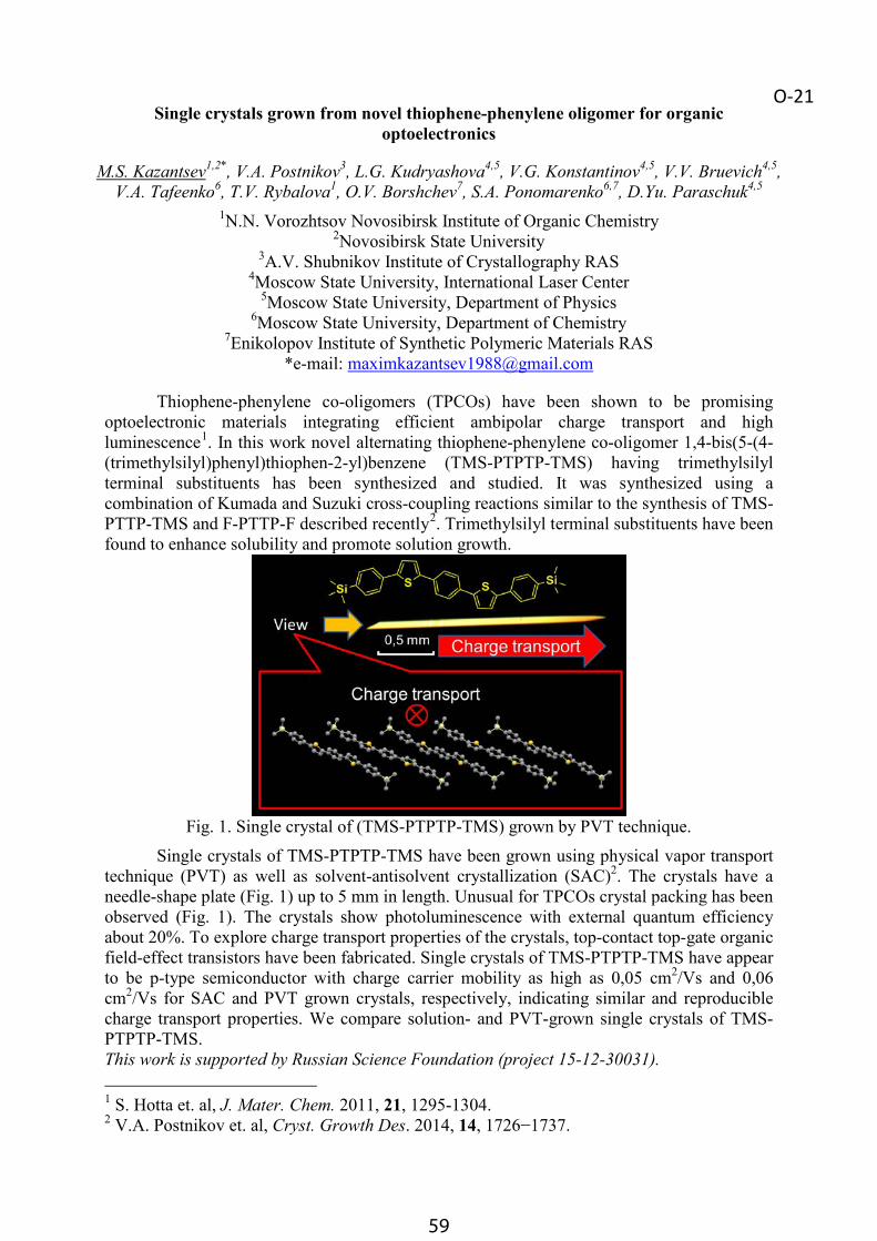
59
Single crystals grown from novel thiophene-phenylene oligomer for organic optoelectronics
M.S. Kazantsev1,2*, V.A. Postnikov3, L.G. Kudryashova4,5, V.G. Konstantinov4,5, V.V. Bruevich4,5,V.A. Tafeenko6, T.V. Rybalova1, O.V. Borshchev7, S.A. Ponomarenko6,7, D.Yu. Paraschuk4,5
1N.N. Vorozhtsov Novosibirsk Institute of Organic Chemistry2Novosibirsk State University
3A.V. Shubnikov Institute of Crystallography RAS4Moscow State University, International Laser Center
5Moscow State University, Department of Physics6Moscow State University, Department of Chemistry
7Enikolopov Institute of Synthetic Polymeric Materials RAS*e-mail: [email protected]
Thiophene-phenylene co-oligomers (TPCOs) have been shown to be promisingoptoelectronic materials integrating efficient ambipolar charge transport and high luminescence1. In this work novel alternating thiophene-phenylene co-oligomer 1,4-bis(5-(4-(trimethylsilyl)phenyl)thiophen-2-yl)benzene (TMS-PTPTP-TMS) having trimethylsilylterminal substituents has been synthesized and studied. It was synthesized using a combination of Kumada and Suzuki cross-coupling reactions similar to the synthesis of TMS-PTTP-TMS and F-PTTP-F described recently2. Trimethylsilyl terminal substituents have been found to enhance solubility and promote solution growth.
Fig. 1. Single crystal of (TMS-PTPTP-TMS) grown by PVT technique.Single crystals of TMS-PTPTP-TMS have been grown using physical vapor transport
technique (PVT) as well as solvent-antisolvent crystallization (SAC)2. The crystals have aneedle-shape plate (Fig. 1) up to 5 mm in length. Unusual for TPCOs crystal packing has been observed (Fig. 1). The crystals show photoluminescence with external quantum efficiency about 20%. To explore charge transport properties of the crystals, top-contact top-gate organic field-effect transistors have been fabricated. Single crystals of TMS-PTPTP-TMS have appear to be p-type semiconductor with charge carrier mobility as high as 0,05 cm2/Vs and 0,06 cm2/Vs for SAC and PVT grown crystals, respectively, indicating similar and reproducible charge transport properties. We compare solution- and PVT-grown single crystals of TMS-PTPTP-TMS.This work is supported by Russian Science Foundation (project 15-12-30031).
1 S. Hotta et. al, J. Mater. Chem. 2011, 21, 1295-1304.2 V.A. Postnikov et. al, Cryst. Growth Des. 2014, 14, 1726−1737.
O-21Benzothiadiazole-based nanostructured organosilicon luminophores for organic
optoelectronics
O.V. Borshchev*1, M.S. Skorotetcky1, N.M. Surin1, E.A. Svidchenko1, Y.V. Fedorov2,S.A. Ponomarenko1,3
1 Enikolopov Institute of Synthetic Polymeric Materials RAS2 Nesmeyanov Institute of Organoelement Compounds RAS
3Moscow State University, Department of Chemistry*e-mail: [email protected]
Recently we have developed a new class of highly efficient luminescent materials with unique properties - nanostructured organosilicon luminophores (NOLs).1 These are branched molecules, where two types of organic chromophores are connected to each other via silicon atoms, which brake the conjugation between them and fix them specifically in the space at 1-2nm distance necessary for efficient Förster energy transfer.2,3,4 NOLs possess several advantages: absorption in a wide optical spectral region; 5–10 times higher absorption cross-sections than those of the best low molar weight organic luminophores; very highphotoluminescence quantum yield; luminescence spectra in the defined wavelength region; short luminescence lifetime. Photoluminescence study of the NOLs has shown an intramolecular energy transfer with the efficiency up to 99% and luminescence quantum yield up to 95% in various spectral regions. It should be noted that combination of different chromophores in NOLs allows tuning their emission wavelengths in a wide spectral region, which open possibilities for their wide application as spectral shifters – convertors of the emission with the energy of high frequency photons (140–400 nm) into emission in the visible spectral range (400–700 nm).5
Benzothiadiazole is one of the most widely used acceptor moieties in low band gap materials for organic electronic applications. Motivation for incorporation of this heterocyclicunit into NOLs is its high absorption coefficient and luminescent quantum yield, large Stocks shift, low bandgap and excellent thermal stability. Thus, we synthesized a series of new NOLs containing benzothiadiazole unit, investigated their optical and thermal properties. The new NOLs obtained were used in various devices of organic photonics and electronics, such as plastic scintillators, spectral shifting fibers, organic light-emitting diodes (OLEDs), organic solar cells (OSCs) and others.
This work was supported by Russian Foundation for Basic Research (Project No. 13-03-12451), Foundation of President of the Russian Federation (project MK 6501.2015.3) andPresidium of the Russian Academy of Sciences (Program No. P-24).
1 S.A. Ponomarenko, N.M. Surin, O.V. Borshchev, Y.N. Luponosov, D.Y. Akimov, I.S. Alexandrov, A.A. Burenkov, A.G. Kovalenko, V.N. Stekhanov, E.A. Kleymyuk, O.T. Gritsenko, G.V. Cherkaev,A.S. Kechek’yan, O.A. Serenko, A.M. Muzafarov Scientific Reports 2014, 4, 6549.
2 O.V. Borshchev, S.A. Ponomarenko, N.M. Surin, M.I. Buzin, A.P. Pleshkova, N.V. Demchenko, V.V. Myakushev, A.M. Muzafarov, Organometallics, 2007, 26, 5165.3 Yu.N. Luponosov, S.A. Ponomarenko, N.M. Surin, O.V. Borshchev, E.A. Shumilkina,
A.M. Muzafarov, Chem. Mater. 2009, 21, 447.4 O.V. Borshchev, Y.N. Luponosov, E.A. Kleymyuk, N.M. Surin, S.A. Ponomarenko, A.M. Muzafarov Russ. Chem. Bull., 2010, 4, 781.
5 D.Y. Akimov, A.V. Akindinov, I.S. Alexandrov, V.A. Belov, O.V. Borshchev, A.A. Burenkov, M.V. Danilov, A.G. Kovalenko, Y.N. Luponosov, S.A. Ponomarenko, V.N. Stekhanov, N.M. Surin, S.A. Zav’yalov, M.Yu. Yablokov, NIM A, 2012, 695, 403-406.

60
Raman spectroscopy as a probe for intermolecular interaction and domain boundaries in organic semiconducting single crystals
E.V. Feldman1, V.V. Bruevich1*, Yu. N. Luponosov2, O.V. Borshchev2, S.A. Ponomarenko2,D.Yu. Paraschuk1
1Faculty of Physics and International Laser Center M.V.Lomonosov MSU2Institute of Synthetic Polymer Materials RAS
*e-mail: [email protected]
Organic semiconducting materials promise the new generation of electronics especially in the light-emitting and photovoltaic applications, such as displays, lighting, solar cells and photodetectors. Thorough understanding of charge transport depending on the material structure is one of the main milestones on the way to an efficient device. Highly ordered organic semiconducting single crystals can be considered as a test bench for studying structure – semiconducting properties correlation on the molecular scale.
Raman spectroscopy is a powerful tool for studying conjugated organic materials atthe molecular level. Importantly, Raman spectroscopy could be used to probe intermolecular interactions using low frequency (LF) Raman spectra1.
Here, we present our recent results on Raman spectroscopy of thiophene−phenelyne co-oligomers (TPCOs) single crystals. These molecules are promising candidates for organic light emitting transistors (OLETs) combining efficient luminescence and charge transport properties. We show that Raman microscopy is sensitive to the orientation of single crystal domains. For that, we analyze the frequency range of covalent C—C vibrations and found clear domain boundaries. We also show that LF Raman spectroscopy can be used as a sensitive tool to study molecular packing and intermolecular interactions in a highly ordered crystalline structure. Fig.1 shows typical dependence of LF Raman spectra of one of the TCPO single crystals on temperature that can be used to analyze the temperature dependence of the molecular order and vibrations.
Fig. 1. (a) Raman spectra for different temperatures; (b) LF Raman peak position dependence on temperature; (c) TPCO chemical structure.
By studying the temperature data for the LF Raman spectra, we correlate the intermolecular vibrations with the crystal structure parameters. The correlation between intermolecular packing, vibrations and the semiconducting properties of the crystals studied are discussed.
This work was supported by RFFI grants 15-02-09375 and 13-02-01313 and M. V. Lomonosov Moscow State University Program of Development.
1 Ando M., et al. Adv. Mater. 2015, 27, 122–129
O-22

61
Towards high performance all printed Organic Field Effect Transistors
S. Conti1*, S. Lai1, P. Cosseddu1, A. Bonfiglio1
1University of Cagliari, Department of Electrical and Electronic Engineering*e-mail: [email protected]
Several examples of Organic Thin-Film Transistor (OTFT) based sensors have been so far proposed in literature, but several technological drawbacks still limit the actual exploitation of the potentialities of organic electronics in the field of biomedical engineering and biorobotics. For instance, Organic Field-Effect Transistors (OFETs) are typically biasedat high voltages (tens of volts), which are not compatible with biological applications. Moreover, the response of OFET-based devices is typically slow, thus impeding their employment for the transduction of several biological signals, such as action potential of electrically active cells. Even if several solutions to these drawbacks have been proposed for small area techniques, less has been done for large area, low-cost fabrication techniques suchas ink-jet printing.
The activity here described is related to the optimization of the printing process of gate dielectrics for high performing, low-voltage OFETs, as the electrical properties of thesedevices strongly depend on the morphological features of the dielectric and on its interface with the semiconductor.
The fabrication of ultra-thin dielectric layers to be used as gate insulator in low voltage OFETs was thoroughly explored. In particular, a homemade poly vinyl phenol (PVP) formulation has been employed. A detailed electrical and morphological characterization hasbeen performed on the printed dielectric layers. Subsequently, bottom gate, bottom contact OFETs have been fabricated. Gate dielectrics have been printed over a pre-patterned aluminum gate electrode, whereas PEDOT:PSS source and drain electrodes have been printed. TIPS-Pentacene was employed as the organic semiconductor, deposited from liquid phase. The optimization of the ink properties on one side, and of the ink-jet printing parameters on the other, allowed obtaining flexible low voltage OFETs with good electrical performances (Figure 1). Thanks to the high capacitive coupling allowed by the ultrathin printed dielectric layer (around 30 nm), the fabricated devices can be operated at very low voltages, as low as 2V, showing hole mobility up to 2.2x10⁻² cm2/Vs, Ion/Ioff up to 103 and remarkably low leakage currents (10 pA). As main outlook, the optimization of the printing process for the gate electrode and for the organic semiconductor will be carried out, in order to obtain fully printed and high performing OFETs.
0.0 -0.4 -0.8 -1.2 -1.6
0.0
-5.0x10⁻⁸
-1.0x10⁻⁷
-1.5x10⁻⁷
-2.0x10⁻⁷
-2.5x10⁻⁷
Id [A
]
Vd [V]
Vg = -0.75V Vg = -1.00V Vg = -1.25V Vg = -1.50V Vg = -1.75V
Figure 1: electrical characterization
O-23

62
Printable multibit resistive memory based on polymer admixtures.
M.S. Kotova1*,M.A. Dronov1, T.V. Dubinina1
1Moscow State University, Department of Physics*e-mail: [email protected]
Development of organic memory devices is one of the major directions of the modern organic electronics. A possibility to construct memory devices from soluble organic materials by different printing technologies demonstrates high potential of the resistive memory (ReRAM). The operating parameters of ReRAM devices meet the requirements for memory applications.
The principles of operation of ReRAM devices presume an ability of the system to switch between at least two states “ON” and “OFF” with different resistances. Resistance of the “OFF” state may exceed the “ON” state resistance by 7 orders of magnitude. Resistive switchings (RS) between these two states occur under application of electric field of arequired magnitude. RS can be reversible and repeatable.
We observed the RS effect in a wide range of organic materials: polymer materialssuch as polystyrene, polycarbonate with and without admixture of metal micro particles1 and photosensitizing dyes on hard substrates in macro and micro spatial scales. For fully inject printing technologies, we studied the possibility of producing printable ReRAM from soluble polymer materials and admixtures on flexible substrates.
We found that the substrate material does not play a major role for the observation of RS. Therefore the RS were observed for all kinds of materials studied on polymer substrates. Optimisation of the sample and the contact area geometries provided the critical electric field needed for switching to the “ON” state less than 10 kV/cm. This value is below the breakdown electric field and is less than value of critical field for macro polymer samples onhard substrates. We also printed up to 25 bits on a single substrate and did not observe any significant crosstalks between neighbouring cells.
We demonstrated a possibility for producing ink-jet printable ReRAM memory devices. This result demonstrates a high potential for construction of printable, efficient andnon-volatile multibit memory devices.
This work was supported by RFBR (project № 14-02-31569, project № 14-03-31579).
1 Kotova M.S., Dronov M.A., Belogorokhov I.A. Bulletin of Moscow State University, 2012,3.2 122501.
O-24

63
Flexible multimodal sensors based on Organic Charge Modulated Thin Film Transistors.
F. Viola*, P. Cosseddu, S. Lai, A. Spanu, A. Bonfiglio1Department of Electrical and Electronic Engineering
University of Cagliari, Piazza d’Armi, 09123Cagliari, Italy
*e-mail: [email protected]
In this work, we introduce a novel approach for the fabrication of temperature and pressure sensors. The devices are based on the integration of an Organic Charge Modulated Field Effect Transistor (OCMFET) with a pyro/piezoelectric polymer element, namely PVDF(Fig. 1.). This transistor configuration has been already employed for different charge sensing systems. The core of the device is a floating gate electrode which is partially covered by a combination of two ultrathin (80 nm) gate dielectrics (namely Al2O3 and Parylene C), thanks to this approach the devices can be operated at voltages as small as 3 V. On this coated area Source, Drain and control Gate electrodes are realized, and finally an organic semiconductor, TIPS-Pentacene, is deposited by drop casting onto the channel of the device. The control gate is used for setting the working point of the sensor. If an additional charge is induced on the floating gate, this perturbation induces a modulation of the charge carriers density in the transistor channel. Consequently, a threshold voltage variation is induced, thus leading to a variation of the device output current. In order to obtain a temperature/pressure sensor, pyro/piezoelectric material based capacitor was connected to the uncoated area (sensing area) of the floating gate. In this case, any temperature/pressure variation in the pyro/piezoelectricelement will induce a charge separation in the device floating gate, thus turning the OCMFET into a temperature/pressure transducer.
Fig. 1. Schematic representation of the OCMFET integrated with a pyro/piezoelectric elementThe electrical characterization of this sensor has demonstrated, as reported in Figure 2
that it is able to clerly detect, in a linear and reproducible way, both Temperature and Pressure (Force). The flexibility of the final straucture and the ease of the fabrication process make thi approach very interesting for a wide range of applications, going from wearable electronics to artificial skin in robotics.
Fig. 2. Current variations VS Temperature (left) and Force (right)
O-25Printable multibit resistive memory based on polymer admixtures.
M.S. Kotova1*,M.A. Dronov1, T.V. Dubinina1
1Moscow State University, Department of Physics*e-mail: [email protected]
Development of organic memory devices is one of the major directions of the modern organic electronics. A possibility to construct memory devices from soluble organic materials by different printing technologies demonstrates high potential of the resistive memory (ReRAM). The operating parameters of ReRAM devices meet the requirements for memory applications.
The principles of operation of ReRAM devices presume an ability of the system to switch between at least two states “ON” and “OFF” with different resistances. Resistance of the “OFF” state may exceed the “ON” state resistance by 7 orders of magnitude. Resistive switchings (RS) between these two states occur under application of electric field of arequired magnitude. RS can be reversible and repeatable.
We observed the RS effect in a wide range of organic materials: polymer materialssuch as polystyrene, polycarbonate with and without admixture of metal micro particles1 and photosensitizing dyes on hard substrates in macro and micro spatial scales. For fully inject printing technologies, we studied the possibility of producing printable ReRAM from soluble polymer materials and admixtures on flexible substrates.
We found that the substrate material does not play a major role for the observation of RS. Therefore the RS were observed for all kinds of materials studied on polymer substrates. Optimisation of the sample and the contact area geometries provided the critical electric field needed for switching to the “ON” state less than 10 kV/cm. This value is below the breakdown electric field and is less than value of critical field for macro polymer samples onhard substrates. We also printed up to 25 bits on a single substrate and did not observe any significant crosstalks between neighbouring cells.
We demonstrated a possibility for producing ink-jet printable ReRAM memory devices. This result demonstrates a high potential for construction of printable, efficient andnon-volatile multibit memory devices.
This work was supported by RFBR (project № 14-02-31569, project № 14-03-31579).
1 Kotova M.S., Dronov M.A., Belogorokhov I.A. Bulletin of Moscow State University, 2012,3.2 122501.

Poster presentations

65
Investigation of temperature stability of single carrier hole only devices
S.Alam1*, C.R. Singh2, H. Hoppe1
1Institute of Physics, Ilmenau University of Technology, Ilmenau, Germany2Department of Macromolecular Chemistry I, Universität Bayreuth, Germany
*e-mail: [email protected]
Thin hole transport layers (HTL) are crucial elements in organic semiconductor based devices. Metal oxides are an encouraging material class for this purpose. Metal oxides can be used to modify either of the two contacts in a device for improved wettability as well as chemical and electronic compatibility of the contacts with the organic layer. Several materials like NiO, V2O5, WO3 and MoO3 have demonstrated encouraging prospective for performing as efficient charge transport layers. Among them molybdenum oxide (MoO3) attracted extensive interest due to its superior performance.
In order to evaluate charge transport properties of annealed semiconductor films, devices are required to be stable at high annealing temperature. Whereas PEDOT:PSS has generally proper charge injection and extraction properties, these may drastically change upon heating above certain temperature. In this work, we show that a MoO3 interlayer can efficiently substitute PEDOT:PSS as hole transport layer within single carrier hole only devices, because of its better stability at high annealing temperature.
P-1
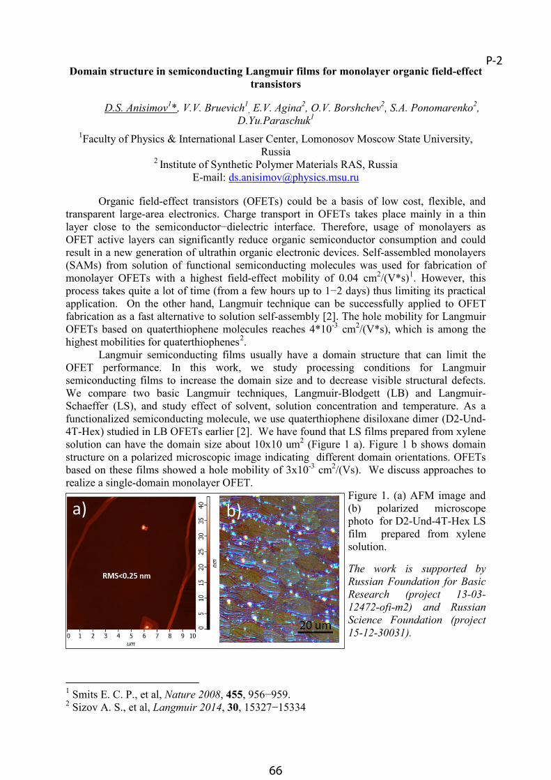
66
Domain structure in semiconducting Langmuir films for monolayer organic field-effect transistors
D.S. Anisimov1*, V.V. Bruevich1, E.V. Agina2, O.V. Borshchev2, S.A. Ponomarenko2,
D.Yu.Paraschuk1
1Faculty of Physics & International Laser Center, Lomonosov Moscow State University, Russia
2 Institute of Synthetic Polymer Materials RAS, RussiaE-mail: [email protected]
Organic field-effect transistors (OFETs) could be a basis of low cost, flexible, and transparent large-area electronics. Сharge transport in OFETs takes place mainly in a thin layer close to the semiconductor−dielectric interface. Therefore, usage of monolayers as OFET active layers can significantly reduce organic semiconductor consumption and could result in a new generation of ultrathin organic electronic devices. Self-assembled monolayers(SAMs) from solution of functional semiconducting molecules was used for fabrication of monolayer OFETs with a highest field-effect mobility of 0.04 cm2/(V*s)1. However, this process takes quite a lot of time (from a few hours up to 1−2 days) thus limiting its practical application. On the other hand, Langmuir technique can be successfully applied to OFET fabrication as a fast alternative to solution self-assembly [2]. The hole mobility for Langmuir OFETs based on quaterthiophene molecules reaches 4*10-3 cm2/(V*s), which is among the highest mobilities for quaterthiophenes2.
Langmuir semiconducting films usually have a domain structure that can limit the OFET performance. In this work, we study processing conditions for Langmuir semiconducting films to increase the domain size and to decrease visible structural defects.We compare two basic Langmuir techniques, Langmuir-Blodgett (LB) and Langmuir-Schaeffer (LS), and study effect of solvent, solution concentration and temperature. As a functionalized semiconducting molecule, we use quaterthiophene disiloxane dimer (D2-Und-4T-Hex) studied in LB OFETs earlier [2]. We have found that LS films prepared from xylene solution can have the domain size about 10x10 um2 (Figure 1 a). Figure 1 b shows domain structure on a polarized microscopic image indicating different domain orientations. OFETs based on these films showed a hole mobility of 3х10-3 cm2/(Vs). We discuss approaches to realize a single-domain monolayer OFET.
Figure 1. (a) AFM image and (b) polarized microscope photo for D2-Und-4T-Hex LS film prepared from xylene solution.
The work is supported by Russian Foundation for Basic Research (project 13-03-12472-ofi-m2) and Russian Science Foundation (project 15-12-30031).
1 Smits E. C. P., et al, Nature 2008, 455, 956−959.2 Sizov A. S., et al, Langmuir 2014, 30, 15327−15334
b)a) b)
P-2

67
Optically induced phenomena in monolayer organic field-effect transistors
A.A. Bakulin1,2*, O. Selig1, H.J. Bakker1, Y.L.A. Rezus1, V.V. Bruevich,3 D.S. Anisimov3,S.A. Ponomarenko4, D.Yu. Paraschuk3
1 FOM Institute AMOLF, Amsterdam, The Netherlands2 Cavendish Laboratory, University of Cambridge, Cambridge UK
3 Faculty of Physics and International Laser Center, Lomonosov Moscow State University, Moscow, Russian Federation
4 Enikolopov Institute of Synthetic Polymeric Materials of Russian Academy of Sciences, Moscow, Russian Federation*e-mail: [email protected]
The strong optical absorption of organic semiconductors combined with powerful modern optical techniques offers a unique opportunity for developing ultrafast and energy efficient optical switching of molecular electronic devices. We have previously demonstrated that molecular systems provide a number of electronic1 and vibronic2 mechanisms for ultrafast optical control of electronic device performance. Yet, important questions remain before this knowledge can be extended to design optically controlled organic field-effecttransistors (OFET). For example, little progress has been made in understanding light-sensitive transistors and their behaviour under external illumination. Such studies are limited by practical constraints including poorly defined transistor channel areas, different dynamics of electrons and holes and the spatial mismatch between charge generation and transport regions.
Fig. 1. The influence of exciting molecular vibrations (blue) in the transistor chanel on the photocurrent produced by the monolayer OFET (red).
Here we apply methodolgy of ultrafast optical spectroscopy to investigate charge dynamics in monolayer OFETs. We study Langmuir OFETs based on quaterthiophene disiloxane dimer (D2-Und-4T-Hex)3 and analyse how photo-doping affects the device parameters under continuous wave illumination as well as under pulsed non-equilibrium conditions. We also show,(fig.1) that excitation of certain modes in the 1200-1600 cm-1
region of D2-Und-4T-Hex leads to photocurrent enhancement. Excited vibrations affect predominantly exciton dissociation in the active layer, which highlights the potential of fast and efficient optical control for both charge and energy transport in organic optoelectronic devices.This work is supported by Russian Foundation for Basic Research, project 15-53-10070_KO_a.
1 Bakulin A.A. et al., Science 335, (2012) 1340.2 Bakulin A.A., et al. arXiv:1503.00777 (2015)3 Sizov et al, Langmuir, 30, (2014) 15327
P-3Domain structure in semiconducting Langmuir films for monolayer organic field-effect
transistors
D.S. Anisimov1*, V.V. Bruevich1, E.V. Agina2, O.V. Borshchev2, S.A. Ponomarenko2,
D.Yu.Paraschuk1
1Faculty of Physics & International Laser Center, Lomonosov Moscow State University, Russia
2 Institute of Synthetic Polymer Materials RAS, RussiaE-mail: [email protected]
Organic field-effect transistors (OFETs) could be a basis of low cost, flexible, and transparent large-area electronics. Сharge transport in OFETs takes place mainly in a thin layer close to the semiconductor−dielectric interface. Therefore, usage of monolayers as OFET active layers can significantly reduce organic semiconductor consumption and could result in a new generation of ultrathin organic electronic devices. Self-assembled monolayers(SAMs) from solution of functional semiconducting molecules was used for fabrication of monolayer OFETs with a highest field-effect mobility of 0.04 cm2/(V*s)1. However, this process takes quite a lot of time (from a few hours up to 1−2 days) thus limiting its practical application. On the other hand, Langmuir technique can be successfully applied to OFET fabrication as a fast alternative to solution self-assembly [2]. The hole mobility for Langmuir OFETs based on quaterthiophene molecules reaches 4*10-3 cm2/(V*s), which is among the highest mobilities for quaterthiophenes2.
Langmuir semiconducting films usually have a domain structure that can limit the OFET performance. In this work, we study processing conditions for Langmuir semiconducting films to increase the domain size and to decrease visible structural defects.We compare two basic Langmuir techniques, Langmuir-Blodgett (LB) and Langmuir-Schaeffer (LS), and study effect of solvent, solution concentration and temperature. As a functionalized semiconducting molecule, we use quaterthiophene disiloxane dimer (D2-Und-4T-Hex) studied in LB OFETs earlier [2]. We have found that LS films prepared from xylene solution can have the domain size about 10x10 um2 (Figure 1 a). Figure 1 b shows domain structure on a polarized microscopic image indicating different domain orientations. OFETs based on these films showed a hole mobility of 3х10-3 cm2/(Vs). We discuss approaches to realize a single-domain monolayer OFET.
Figure 1. (a) AFM image and (b) polarized microscope photo for D2-Und-4T-Hex LS film prepared from xylene solution.
The work is supported by Russian Foundation for Basic Research (project 13-03-12472-ofi-m2) and Russian Science Foundation (project 15-12-30031).
1 Smits E. C. P., et al, Nature 2008, 455, 956−959.2 Sizov A. S., et al, Langmuir 2014, 30, 15327−15334
b)a) b)
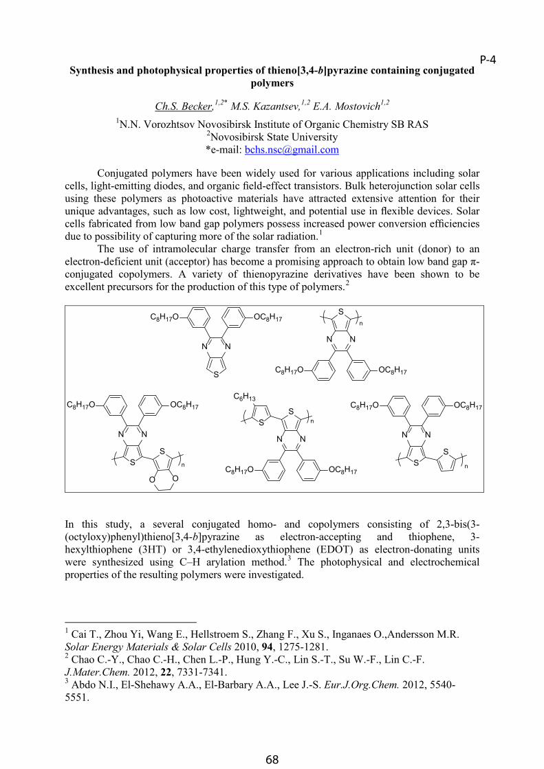
68
Synthesis and photophysical properties of thieno[3,4-b]pyrazine containing conjugated polymers
Ch.S. Becker,1,2* M.S. Kazantsev,1,2 E.A. Mostovich1,2
1N.N. Vorozhtsov Novosibirsk Institute of Organic Chemistry SB RAS2Novosibirsk State University*e-mail: [email protected]
Conjugated polymers have been widely used for various applications including solar cells, light-emitting diodes, and organic field-effect transistors. Bulk heterojunction solar cells using these polymers as photoactive materials have attracted extensive attention for their unique advantages, such as low cost, lightweight, and potential use in flexible devices. Solar cells fabricated from low band gap polymers possess increased power conversion efficiencies due to possibility of capturing more of the solar radiation.1
The use of intramolecular charge transfer from an electron-rich unit (donor) to an electron-deficient unit (acceptor) has become a promising approach to obtain low band gap π-conjugated copolymers. A variety of thienopyrazine derivatives have been shown to be excellent precursors for the production of this type of polymers.2
S
NN
OC8H17C8H17O S
NN
OC8H17C8H17O
S
N N
C8H17O OC8H17
S
S
NN
OC8H17C8H17O
S
O O
C6H13
S
NN
OC8H17C8H17O
S
n
nn
n
In this study, a several conjugated homo- and copolymers consisting of 2,3-bis(3-(octyloxy)phenyl)thieno[3,4-b]pyrazine as electron-accepting and thiophene, 3-hexylthiophene (3HT) or 3,4-ethylenedioxythiophene (EDOT) as electron-donating unitswere synthesized using C–H arylation method.3 The photophysical and electrochemicalproperties of the resulting polymers were investigated.
1 Cai T., Zhou Yi, Wang E., Hellstroem S., Zhang F., Xu S., Inganaes O.,Andersson M.R. Solar Energy Materials & Solar Cells 2010, 94, 1275-1281.2 Chao C.-Y., Chao C.-H., Chen L.-P., Hung Y.-C., Lin S.-T., Su W.-F., Lin C.-F.J.Mater.Chem. 2012, 22, 7331-7341.3 Abdo N.I., El-Shehawy A.A., El-Barbary A.A., Lee J.-S. Eur.J.Org.Chem. 2012, 5540-5551.
P-4
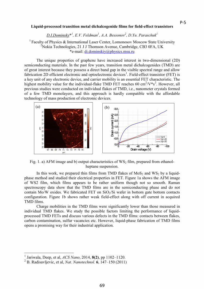
69
0 -20 -40 -60 -80 -1000,0
-0,5
-1,0
-1,5
-2,0
-2,5
-3,0Dr
ain
curr
ent (
nA)
Drain voltage (V)
Vg=0Vg=-20Vg=-50
Liquid-processed transition metal dichalcogenide films for field-effect transistors
D.I.Dominsky*1, E.V. Feldman1, A.A. Bessonov2, D.Yu. Paraschuk1
1 Faculty of Physics & International Laser Center, Lomonosov Moscow State University 2Nokia Technologies, 21 J J Thomson Avenue, Cambridge, CB3 0FA, UK
*e-mail: [email protected]
The unique properties of graphene have increased interest in two-dimensional (2D) semiconducting materials. In the past few years, transition metal dichalcogenides (TMD) are of great interest because they possess a direct band gap in the visible spectral range and allow fabrication 2D efficient electronic and optoelectronic devices1. Field-effect transistor (FET) is a key unit of any electronic device, and carrier mobility is an essential FET characteristic. The highest mobility value for the individual-flake TMD FET reaches 60 cm2/V*s2. However, allprevious studies were conducted on individual flakes of TMD, i.e., nanometer crystals formed of a few TMD monolayers, and this approach is hardly compatible with the affordabletechnology of mass production of electronic devices.
Fig. 1. a) AFM image and b) output characteristics of WS2 film, prepared from ethanol-heptane suspension.
In this work, we prepared thin films from TMD flakes of MoS2 and WS2 by a liquid-phase method and studied their electrical properties in FET. Figure 1a shows the AFM image of WS2 film, which films appears to be rather uniform though not so smooth. Raman spectroscopy data show that the TMD films are in the semiconducting phase and do not contain Mo/W oxides. We fabricated FET on SiO2/Si wafer in bottom gate bottom contacts configuration. Figure 1b shows rather weak field-effect along with off current in acquiredTMD films.
Charge mobilities in the TMD films were significantly lower than those measured in individual TMD flakes. We study the possible factors limiting the performance of liquid-processed TMD FETs and discuss various defects in the TMD films: contacts between flakes,carbon contamination, sulfur vacancies etc. However, liquid-phase fabrication of TMD films opens a promising way for their industrial application.
1 Jariwala, Deep, et al, ACS Nano, 2014, 8(2), pp 1102–1120.2 B. Radisavljevic, et al, Nat. Nanotechnol. 6, 147–150 (2011)
(a) (b)
P-5Synthesis and photophysical properties of thieno[3,4-b]pyrazine containing conjugated
polymers
Ch.S. Becker,1,2* M.S. Kazantsev,1,2 E.A. Mostovich1,2
1N.N. Vorozhtsov Novosibirsk Institute of Organic Chemistry SB RAS2Novosibirsk State University*e-mail: [email protected]
Conjugated polymers have been widely used for various applications including solar cells, light-emitting diodes, and organic field-effect transistors. Bulk heterojunction solar cells using these polymers as photoactive materials have attracted extensive attention for their unique advantages, such as low cost, lightweight, and potential use in flexible devices. Solar cells fabricated from low band gap polymers possess increased power conversion efficiencies due to possibility of capturing more of the solar radiation.1
The use of intramolecular charge transfer from an electron-rich unit (donor) to an electron-deficient unit (acceptor) has become a promising approach to obtain low band gap π-conjugated copolymers. A variety of thienopyrazine derivatives have been shown to be excellent precursors for the production of this type of polymers.2
S
NN
OC8H17C8H17O S
NN
OC8H17C8H17O
S
N N
C8H17O OC8H17
S
S
NN
OC8H17C8H17O
S
O O
C6H13
S
NN
OC8H17C8H17O
S
n
nn
n
In this study, a several conjugated homo- and copolymers consisting of 2,3-bis(3-(octyloxy)phenyl)thieno[3,4-b]pyrazine as electron-accepting and thiophene, 3-hexylthiophene (3HT) or 3,4-ethylenedioxythiophene (EDOT) as electron-donating unitswere synthesized using C–H arylation method.3 The photophysical and electrochemicalproperties of the resulting polymers were investigated.
1 Cai T., Zhou Yi, Wang E., Hellstroem S., Zhang F., Xu S., Inganaes O.,Andersson M.R. Solar Energy Materials & Solar Cells 2010, 94, 1275-1281.2 Chao C.-Y., Chao C.-H., Chen L.-P., Hung Y.-C., Lin S.-T., Su W.-F., Lin C.-F.J.Mater.Chem. 2012, 22, 7331-7341.3 Abdo N.I., El-Shehawy A.A., El-Barbary A.A., Lee J.-S. Eur.J.Org.Chem. 2012, 5540-5551.
70
Modeling resistive switching in organic-based ReRAM
M.A. Dronov1,2*, M.S. Kotova1, I.A Belogorokhov.21M.V. Lomonosov Moscow State University, Moscow, Russian Federation
2Federal State Research and Design Institute of Rare Metal Industry ("Giredmet"), Moscow, Russian Federation
*e-mail: [email protected]
Resistive switching, the reversible modulation of electronic conductivity, is of interest for prospective memory devices that could be a perfect electronic memory. Though different types of ReRAM (Resistive Random Access Memory) exist, the organic based ReRAM is of a special interest due to the possibility for production of high performance devices using arelatively simple technology.
Despite recent advantages in understanding of underlying physical mechanisms for resistive switching, there is still a relatively large set of experimental data that cannot be explained. The five main mechanisms of the resistive switching are: the phase change mechanism (PCM), the thermo-chemical mechanism (TCM), the valency change mechanism (VCM), the electro-chemical metallisation (ECM) and the electrostatic/electronic mechanism (EEM). The problem is that for the widely observed unipolar switching only PCM and TCM are applicable which often seems to be not possible in organic materials, while all other mechanisms require the bipolar behaviour, with channels forming/dissolving (for VCM or ECM) with different voltage polarities.
We demonstrated previously1,2 that admixture of photosensitive molecules to the polymer switching layer may lead to addition of two effects to the conventional resistive switching (controlled by electric field). The first one is the photo-induced switching (i.e. nonvolatile change in the resistance controlled by light), the second is the photo-controllable switching (i.e. change of critical switching parameters under illumination).
We suggest an adaptation and extension for the model used for filament thermal dissolution in NiO metal-insulator-metal switches3. Our main extension to the model is to account for charge carrier generation under illumination as an effective modification to the filament electrical resistance.
The calculated filament parameters match reasonably with estimates for silver based filaments. This result provides an argument supporting a filament formation from the contact material though other options are possible.
This work was supported by RFBR (project 14-02-31569) and by Federal Target Grant "Research and development on priority Areas of Science and Technology Complex of Russia for 2014-2020" (government contract 14.576.21.0029 Unique identifier for Applied Scientific Research (project) RFMEFI57614X0029).
1 M. Dronov, I. Belogorohov and D. Khokhlov (2011). New MEH-PPV Based Composite Materials for Rewritable Nonvolatile Polymer Memory Devices. MRS Proceedings, 1337,mrss11-1337-q05-07 doi:10.1557/opl.2011.980.2 M. Dronov, M. Kotova and I. Belogorohov (2015). Photo-controllable Resistive Memory Based on Polymer Materials. MRS Proceedings, 1729, mrsf14-1729-m02-08doi:10.1557/opl.2015.289.3 U. Russo, D. Ielmini, C. Cagli, A.L. Lacaita: Self-accelerated thermal dissolution model for reset programming in unipolar resistive-switching memory (RRAM) devices. IEEE Trans. Electron Devices 56(2), 193–200 (2009)
P-6

71
Influence of solvent vapor annealing on the performance of organic solar cells
F. Drozdov1, Yu. Luponosov1, А. Gavrik2, V. Dyakonov2, S. Ponomarenko1
1Institute of Synthetic Polymer Materials RAS2Julius Maximilian University of Würzburg
*e-mail: [email protected]
It is well known that performance of the organic solar cells (OSCs) strongly depends on the properties of functional materials used for their preparation, including their energy levels, band gap, light absorption efficiency, charge carriers mobility, etc. However, for achieving the best device performance, some other parameters, namely active layer morphology and uniformity need to be taken into consideration. These parameters influence on the efficiency of charges dissociation and transport processes in the active layer and, consequently, can significantly change short circuit current (Isc) and fill factor (FF) of the OSC. There are a few methods to improve the active layer morphology: thermal annealing, usage of additives and vapor solvent annealing. The last method is based on changingmolecular ordering in the bulk by treating the active layer by vapors of a good solvent. In the case of OSCs, this method can lead to a significantly optimization of the donor : acceptor domain structure.
In this work two low bandgap copolymers, pCPDT-DTBT and pCPDT-DFCPDT, and two small molecules, DTS(Oct)2-(2T-DCV-Me)2 and DTS(EH)2-(2T-DCV-Me)2, were selected as donor parts and PC71BM as acceptor, from mixtures of which OSCs with common architecture ITO/PEDOT:PSS/donor:PCBM70/Ca,Al were prepared. Active layers were deposited by spin-coating from mixture with chlorobenzene in the inert atmosphere. In the case of the small molecules based OSCs, the ratio of donor:acceptor mixture was 1:1 and 3:1, while it was 1:1in the case of copolymers based OSCs. After deposition of the layer active,the devices were treated in the atmosphere of chloroform by a fixed time: 90 sec for OSCs based on small molecules and 120, 300, 420 sec for copolymers-based OSCs.
S
Si
SS S
S SNC CN CNNC
R R
SS
RR
SS
FFn
R=
S
S
NS
N
RR
SS
n
R=
R=
pCPDT-DTBTpCPDT-DFCPDT
DTS(Oct)2-(2T-DCV-Me)2
DTS(EH)2-(2T-DCV-Me)2
It was shown that the power conversion efficiency (PCE) of annealed OSCs based onDTS(Oct)2-(2T-DCV-Me)2 increased from 1,15% to 2,2% as compared to not annealed OSCs,but in the case of DTS(EH)2-(2T-DCV-Me)2 PCE was not changed. For the copolymers-based OSCs the maximum of PCE = 2,97% comparing with 1,5% was achieved.
Thus, as a result, in the case of DTS(Oct)2-(2T-DCV-Me)2 and copolymers, more crystallinity character of molecules allows to improve morphology of OSCs active layer in bulk and, as consequence, total PCE, but not in the case of amorphous molecules of DTS(EH)2-(2T-DCV-Me)2.This work was supported by RFBR (project № 15-33-20957).
P-7Modeling resistive switching in organic-based ReRAM
M.A. Dronov1,2*, M.S. Kotova1, I.A Belogorokhov.21M.V. Lomonosov Moscow State University, Moscow, Russian Federation
2Federal State Research and Design Institute of Rare Metal Industry ("Giredmet"), Moscow, Russian Federation
*e-mail: [email protected]
Resistive switching, the reversible modulation of electronic conductivity, is of interest for prospective memory devices that could be a perfect electronic memory. Though different types of ReRAM (Resistive Random Access Memory) exist, the organic based ReRAM is of a special interest due to the possibility for production of high performance devices using arelatively simple technology.
Despite recent advantages in understanding of underlying physical mechanisms for resistive switching, there is still a relatively large set of experimental data that cannot be explained. The five main mechanisms of the resistive switching are: the phase change mechanism (PCM), the thermo-chemical mechanism (TCM), the valency change mechanism (VCM), the electro-chemical metallisation (ECM) and the electrostatic/electronic mechanism (EEM). The problem is that for the widely observed unipolar switching only PCM and TCM are applicable which often seems to be not possible in organic materials, while all other mechanisms require the bipolar behaviour, with channels forming/dissolving (for VCM or ECM) with different voltage polarities.
We demonstrated previously1,2 that admixture of photosensitive molecules to the polymer switching layer may lead to addition of two effects to the conventional resistive switching (controlled by electric field). The first one is the photo-induced switching (i.e. nonvolatile change in the resistance controlled by light), the second is the photo-controllable switching (i.e. change of critical switching parameters under illumination).
We suggest an adaptation and extension for the model used for filament thermal dissolution in NiO metal-insulator-metal switches3. Our main extension to the model is to account for charge carrier generation under illumination as an effective modification to the filament electrical resistance.
The calculated filament parameters match reasonably with estimates for silver based filaments. This result provides an argument supporting a filament formation from the contact material though other options are possible.
This work was supported by RFBR (project 14-02-31569) and by Federal Target Grant "Research and development on priority Areas of Science and Technology Complex of Russia for 2014-2020" (government contract 14.576.21.0029 Unique identifier for Applied Scientific Research (project) RFMEFI57614X0029).
1 M. Dronov, I. Belogorohov and D. Khokhlov (2011). New MEH-PPV Based Composite Materials for Rewritable Nonvolatile Polymer Memory Devices. MRS Proceedings, 1337,mrss11-1337-q05-07 doi:10.1557/opl.2011.980.2 M. Dronov, M. Kotova and I. Belogorohov (2015). Photo-controllable Resistive Memory Based on Polymer Materials. MRS Proceedings, 1729, mrsf14-1729-m02-08doi:10.1557/opl.2015.289.3 U. Russo, D. Ielmini, C. Cagli, A.L. Lacaita: Self-accelerated thermal dissolution model for reset programming in unipolar resistive-switching memory (RRAM) devices. IEEE Trans. Electron Devices 56(2), 193–200 (2009)

72
Single-molecular junctions based on polyaniline molecules and single-walled carbon nanotubes contacts
A.V. Emelianov, A.V. Romashkin, K.A. Tsarik, M.G. Guschin, I.I. BobrinetskiyNational Research University of Electronic Technology
*e-mail: [email protected]
The ability to control the conductance of single molecules will have a major impact in nanoscale electronics. Understanding electron conduction in atomic and molecular scale nanodevices can be achieved from formation of molecular channels. In clear contrast to gold electrodes, the nanotubes can act as true nanoscale electrodes and the properties of the junction may be dramatically modified by changing the topology of the contacts between the nanotubes and the molecules. However, the fabrication of reliable, nanometer-sized gaps separating two contacts remains one of the main challenges for the implementation of carbon-based electrodes.
Single-walled carbon nanotubes (SWCNTs) were provided by Professor A. Nasibulin (Skoltech). They were grown on Si/SiO2 substrate using gas-phase process formation based on thermal decomposition of ferrocene in the presence of carbon monoxide. Source and drain 100/5 nm Au/Cr electrodes were fabricated by photolithography, the gate electrode was high doped Si substrate. Using focused ion beam we cut SWCNTs and made a gap ~ 30-60 nm(Fig. 1). Polyaniline (PANI) molecules in emeraldine base form with an average molecular weight ~ 10000 were used as an organic channel between two formed SWCNTs. It is worth noting that the conductance of this form of PANI is ~ 1×10⁻⁹ S/cm. PANI molecules were deposited on a substrate using drop-coating technique. The concentration of the solution was 0.01 mg/ml and the volume of the drop was 0.2 µl. After that current-voltage (Fig. 2), optical and morphological characteristics of fabricated devices have been measured.
Using SWCNTs as contacts allow us to create highly conductive molecular junctionsbased on PANI molecules. It may be possible because SWCNTs have a high ability to inject charge and as they are true nanoscale electrodes. It helps us to understand transport mechanisms in organic molecules by varying a gate voltage that leads to change the properties of molecules. The average conductance of formed devices was about 3,2×10⁻³ S/cm (for doped PANI – 1-2 S/cm) and linear mobility ~ 2,2 cm2/V×s Thus, we showed the possibility of making a functional molecular device using single molecules as an active channel and the ability to control of its properties.
Fig. 1. SEM image of the cutting SWCNT using FIB between two Au contacts
Fig. 2. Transfer C-V curve for SWCNT and for molecular junction based on PANI
molecules and SWCNTs contacts
P-8
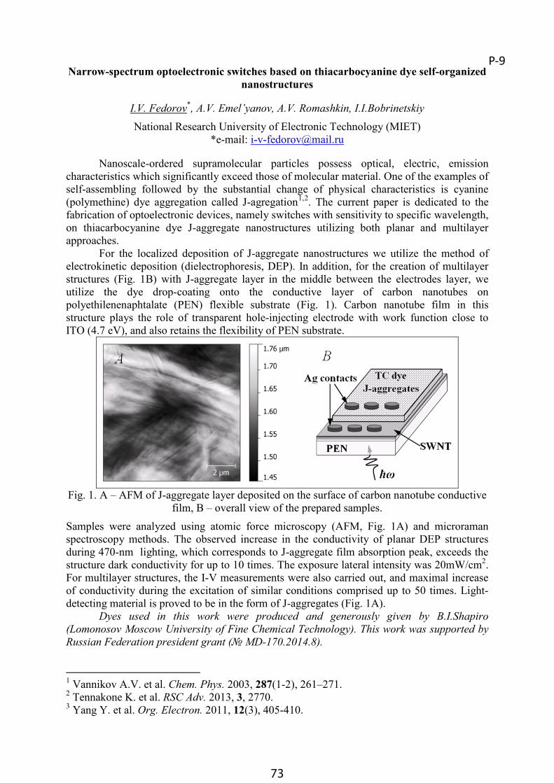
73
Narrow-spectrum optoelectronic switches based on thiacarbocyanine dye self-organizednanostructures
I.V. Fedorov*, A.V. Emel’yanov, A.V. Romashkin, I.I.BobrinetskiyNational Research University of Electronic Technology (MIET)
*e-mail: [email protected]
Nanoscale-ordered supramolecular particles possess optical, electric, emission characteristics which significantly exceed those of molecular material. One of the examples of self-assembling followed by the substantial change of physical characteristics is cyanine (polymethine) dye aggregation called J-agregation1,2. The current paper is dedicated to the fabrication of optoelectronic devices, namely switches with sensitivity to specific wavelength, on thiacarbocyanine dye J-aggregate nanostructures utilizing both planar and multilayer approaches.
For the localized deposition of J-aggregate nanostructures we utilize the method of electrokinetic deposition (dielectrophoresis, DEP). In addition, for the creation of multilayer structures (Fig. 1B) with J-aggregate layer in the middle between the electrodes layer, we utilize the dye drop-coating onto the conductive layer of carbon nanotubes on polyethilenenaphtalate (PEN) flexible substrate (Fig. 1). Carbon nanotube film in this structure plays the role of transparent hole-injecting electrode with work function close to ITO (4.7 eV), and also retains the flexibility of PEN substrate.
Fig. 1. A – AFM of J-aggregate layer deposited on the surface of carbon nanotube conductive film, B – overall view of the prepared samples.
Samples were analyzed using atomic force microscopy (AFM, Fig. 1A) and microraman spectroscopy methods. The observed increase in the conductivity of planar DEP structures during 470-nm lighting, which corresponds to J-aggregate film absorption peak, exceeds the structure dark conductivity for up to 10 times. The exposure lateral intensity was 20mW/cm2.For multilayer structures, the I-V measurements were also carried out, and maximal increase of conductivity during the excitation of similar conditions comprised up to 50 times. Light-detecting material is proved to be in the form of J-aggregates (Fig. 1A).
Dyes used in this work were produced and generously given by B.I.Shapiro (Lomonosov Moscow University of Fine Chemical Technology). This work was supported byRussian Federation president grant (№ MD-170.2014.8).
1 Vannikov A.V. et al. Chem. Phys. 2003, 287(1-2), 261–271.2 Tennakone K. et al. RSC Adv. 2013, 3, 2770.3 Yang Y. et al. Org. Electron. 2011, 12(3), 405-410.
P-9Single-molecular junctions based on polyaniline molecules and single-walled carbon
nanotubes contacts
A.V. Emelianov, A.V. Romashkin, K.A. Tsarik, M.G. Guschin, I.I. BobrinetskiyNational Research University of Electronic Technology
*e-mail: [email protected]
The ability to control the conductance of single molecules will have a major impact in nanoscale electronics. Understanding electron conduction in atomic and molecular scale nanodevices can be achieved from formation of molecular channels. In clear contrast to gold electrodes, the nanotubes can act as true nanoscale electrodes and the properties of the junction may be dramatically modified by changing the topology of the contacts between the nanotubes and the molecules. However, the fabrication of reliable, nanometer-sized gaps separating two contacts remains one of the main challenges for the implementation of carbon-based electrodes.
Single-walled carbon nanotubes (SWCNTs) were provided by Professor A. Nasibulin (Skoltech). They were grown on Si/SiO2 substrate using gas-phase process formation based on thermal decomposition of ferrocene in the presence of carbon monoxide. Source and drain 100/5 nm Au/Cr electrodes were fabricated by photolithography, the gate electrode was high doped Si substrate. Using focused ion beam we cut SWCNTs and made a gap ~ 30-60 nm(Fig. 1). Polyaniline (PANI) molecules in emeraldine base form with an average molecular weight ~ 10000 were used as an organic channel between two formed SWCNTs. It is worth noting that the conductance of this form of PANI is ~ 1×10⁻⁹ S/cm. PANI molecules were deposited on a substrate using drop-coating technique. The concentration of the solution was 0.01 mg/ml and the volume of the drop was 0.2 µl. After that current-voltage (Fig. 2), optical and morphological characteristics of fabricated devices have been measured.
Using SWCNTs as contacts allow us to create highly conductive molecular junctionsbased on PANI molecules. It may be possible because SWCNTs have a high ability to inject charge and as they are true nanoscale electrodes. It helps us to understand transport mechanisms in organic molecules by varying a gate voltage that leads to change the properties of molecules. The average conductance of formed devices was about 3,2×10⁻³ S/cm (for doped PANI – 1-2 S/cm) and linear mobility ~ 2,2 cm2/V×s Thus, we showed the possibility of making a functional molecular device using single molecules as an active channel and the ability to control of its properties.
Fig. 1. SEM image of the cutting SWCNT using FIB between two Au contacts
Fig. 2. Transfer C-V curve for SWCNT and for molecular junction based on PANI
molecules and SWCNTs contacts

74
Tip-enhanced Raman spectroscopy as a probe for organic bulk heterojunction and semiconducting monolayers
E.V. Feldman1, A.A. Mannanov1, V.V. Bruevich1, O.V. Kozlov1, A.Yu. Gavrik1, D. Yu. Paraschuk1
1 Lomonosov Moscow State University, Department of Physics & International Laser Center*e-mail: [email protected]
Combination of high spatial resolution with chemical selectivity is an great demand for probing organic electronics materials. The maximum spatial resolution achievable in Raman microscopy is limited by approximately half the wavelength of the Raman excitation. Tip-enhanced Raman Spectroscopy (TERS) overcomes these limitations by combining scanning probe microscopy and Raman spectroscopy. TERS allows obtaining localized molecular vibrational information with a spatial resolution reaching 10 nm1.
Despite serious effort, TERS technique has not yet evolved to a commonly used spectroscopic method. Samples that can be efficiently studied by TERS are very limited. In organic electronics, where microscopic analysis with chemical selectivity at the nanometer scale is particularly in demand, practical implementation of TERS has met additional difficulties. Attempts to study organic bulk heterojunction materials using TERS microscopy were not successful because of tip degradation during the scanning. However, TERS was used to record of the local Raman spectra in selected points on the sample2.
In the present work, we used TERS to study bulk heterojunction morphology inultrathin polymer-fullerene blends and semiconducting monolayers. We have evaluated two approaches to observe TERS in the scanning mode: a metal tip in the tunneling mode and ametallized AFM cantilever in the semi-contact mode. For each approach, we have optimizedparameters of the scanning probe (material, hardness and radius). We optimized thefabrication of probes to achieve a tip radius less than 30nm (Fig. 1(a)). This allowed us to obtain a spectral map of P3HT:PCBM with submicrometer spatial resolution (Fig. 1(b)). Also we have successfully recorded a Raman spectrum of quaterthiophene siloxane dimer monolayer film3 by using TERS that can substantially increase the Raman signal (Fig. 1(c)).
Fig. 1. a) SEM image of a silver probe; b) Spectral map of a P3HT:PCBM film in the scanning mode; c) Spectral map of tip-enhanced Raman intensity of quaterthiophene siloxane
dimer monolayer film. Maximum of intensity is observed close to the fixed tip.We discuss fabrication of probes, different approaches of measuring, and other issues
related to TERS in organic electronics. Our results indicate that the TERS technique is a promising tool for organic electronics.This work was supported by Russian Science Foundation (project 15-12-30031) and done using equipment supplied by M.V. Lomonosov Moscow State University Program of Development.
1 N. Hayazawa et al. Raman Spectroscopy for Nanomaterials Characterization. 2012, 445–476.2 Xiao Wang et al. Adv. Funct. Mater. 2010, 20, 492–499.3 Sizov A. S. et al. Langmuir, v.30, №50, 15327-15334 (2014).
P-10

75
Synthesis of CH3NH3PbI3/TiO2 films in solvothermal and supercritical fluids
A. V. Grigorieva1*, N. A. Belich1, S. V. Balakhonov1, S. Z. Vatsadze2, E. A. Goodilin1,2
1Moscow State University, Department of Materials Science2Moscow State University, Department of Chemistry
*e-mail: [email protected]
One of the most perspective trends of current development of alternative energy is related to “all solid” solar cells. A great challenge is now deals with new organic-inorganic perovskites providing solar cell efficiency above 20.1%. The number of publications related on perovskite dye compounds grows up remarkably for the last five years. The modern photovoltaic elements supposes deep modifications of the original Graetzel element of 1991, the most important innovation is application of a special sensitizer which effectively absorbslight in the visible and near IR range.
Micromorphology and crystal structure of the perovskite-like dye compounds are keyfactors which influence on absorption and charge transport of the materials. Organic-inorganic compounds are especially apposite example of the materials with anisotropy. This motivates to analyze dye compounds of faced differently.
All experiments were performed in double excess of methylammonium iodide to PbI2in the liquor. That was demonstrated that the solvothermal growth of CH3NH3PbI3 in propanol-2 media leads to prismatic shape of crystallites contrary to cube-like obtained via recrystallization in air. Increasing temperature of the treatment the micron- and submicron-sized crystallites of the pure CH3NH3PbI3 phase of tetragonal lead-methylammonium iodide were obtained. An increase of pressure in the system up to 100 bar at 250°C produced the crystallites of tetragonal CH3NH3PbI3 of cage-like morphology with rather rough (100) planes.
Supercritical fluids of CO2-propanol-2 were proposed as the perfect media for the synthesis of CH3NH3PbI3/TiO2 composite films by transport reaction. This work was supported by RFBR (project № 13-03-01143).
P-11Tip-enhanced Raman spectroscopy as a probe for organic bulk heterojunction and
semiconducting monolayers
E.V. Feldman1, A.A. Mannanov1, V.V. Bruevich1, O.V. Kozlov1, A.Yu. Gavrik1, D. Yu. Paraschuk1
1 Lomonosov Moscow State University, Department of Physics & International Laser Center*e-mail: [email protected]
Combination of high spatial resolution with chemical selectivity is an great demand for probing organic electronics materials. The maximum spatial resolution achievable in Raman microscopy is limited by approximately half the wavelength of the Raman excitation. Tip-enhanced Raman Spectroscopy (TERS) overcomes these limitations by combining scanning probe microscopy and Raman spectroscopy. TERS allows obtaining localized molecular vibrational information with a spatial resolution reaching 10 nm1.
Despite serious effort, TERS technique has not yet evolved to a commonly used spectroscopic method. Samples that can be efficiently studied by TERS are very limited. In organic electronics, where microscopic analysis with chemical selectivity at the nanometer scale is particularly in demand, practical implementation of TERS has met additional difficulties. Attempts to study organic bulk heterojunction materials using TERS microscopy were not successful because of tip degradation during the scanning. However, TERS was used to record of the local Raman spectra in selected points on the sample2.
In the present work, we used TERS to study bulk heterojunction morphology inultrathin polymer-fullerene blends and semiconducting monolayers. We have evaluated two approaches to observe TERS in the scanning mode: a metal tip in the tunneling mode and ametallized AFM cantilever in the semi-contact mode. For each approach, we have optimizedparameters of the scanning probe (material, hardness and radius). We optimized thefabrication of probes to achieve a tip radius less than 30nm (Fig. 1(a)). This allowed us to obtain a spectral map of P3HT:PCBM with submicrometer spatial resolution (Fig. 1(b)). Also we have successfully recorded a Raman spectrum of quaterthiophene siloxane dimer monolayer film3 by using TERS that can substantially increase the Raman signal (Fig. 1(c)).
Fig. 1. a) SEM image of a silver probe; b) Spectral map of a P3HT:PCBM film in the scanning mode; c) Spectral map of tip-enhanced Raman intensity of quaterthiophene siloxane
dimer monolayer film. Maximum of intensity is observed close to the fixed tip.We discuss fabrication of probes, different approaches of measuring, and other issues
related to TERS in organic electronics. Our results indicate that the TERS technique is a promising tool for organic electronics.This work was supported by Russian Science Foundation (project 15-12-30031) and done using equipment supplied by M.V. Lomonosov Moscow State University Program of Development.
1 N. Hayazawa et al. Raman Spectroscopy for Nanomaterials Characterization. 2012, 445–476.2 Xiao Wang et al. Adv. Funct. Mater. 2010, 20, 492–499.3 Sizov A. S. et al. Langmuir, v.30, №50, 15327-15334 (2014).

76
Synthesis of ASnI3 (A=Cs+, CH3NH3+) perovskite-like structures and their optical
performance
A.-A.D. Guseynov1*, A. V. Grigorieva1, E. A. Goodilin1
1Moscow State University, Department of Chemistry.*e-mail: [email protected]
Light-absorbing tin halide perovskites are the subject of increasing number of research projects in the field of inorganic chemistry of organic-inorganic halides. Such halides are mainly using as sensitizers in Grätzel cells. In distinction from mostly using in this field lead halide perovskites tin-based compounds are non-toxic. More than that, tin-based perovskites show better light absorption than lead analogues due to smaller band gap. Among thedisadvantages of such sensitizers is their rapid degradation under ambient conditions.Stabilization of tin halide perovskites is one of the most important problems connected with their wide application in solar cells.
In April 2014 first solar cell using completely lead-free tin halide perovskite (tinmethylammonium iodide) as a sensitizer was studied; efficiency of this device was over 6 %,VOC ~ 0.88V, energy losses (defined as the difference between band gap and open circuit voltage multiplied by the electron charge) was 0.35 eV that is near to same characteristic of silicon-based cell. Considerable degradation of tin methylammonium iodide (which may undergo both of these processes) may be noted after 2 hours of staying of samples in open air1. It is important that even degraded samples shows good light absorption. From of the allthree-dimensional tin halide perovskites, tin methylammonium iodide (CH3NH3SnI3), tin formamidium iodide (HC(NH2)2SnI3) and tin cesium iodide (CsSnI3) are most often considering in literature. All of these compounds show good light absorption in visible and UV region.
In this work we synthesized three-dimensional tin halide perovskites: tin cesium iodide and tin methylammonium iodide. Both these compounds were crystallized from solution with variation of solvent (2-propanol or water), temperature and inertness of atmosphere. Absorption spectra of the samples show the absorption edge at ~950 nm which corresponds to the band gap ~1.3 eV which is near to the data described in literature Samples obtained from water solution by heating under inert atmosphere were the most homogenous due to respectively small solubility of oxygen in water and short time of staying samples under atmosphere that may have admixture of oxygen. After that we studied absorption spectra of thin films of these compounds crystallized from water solution (with heating under inert atmosphere) on glass and mesoporous TiO2. Two-phase thin films of tin halide perovskites with general formula Csx(CH3NH3)1-xSnI3 (where x = 0.1, 0.5 and 0.9) on glass were obtained and their absorption spectra was also investigated. Degradation of CsSnI3 and CH3NH3SnI3 films was studied by XRD. After all, we studied absorption spectrum of Cs2SnI6which may be used as air-stable sensitizer in Grätzel cells. As it may be seen from absorption spectra, all the samples of perovskites are not completely single phase but strong absorption peak on ~1.3 eV typical for these perovskites is present. The main admixture is presumably tin tetraiodide (it may cause absorption peak in blue region). Perovskites with general formula Csx(CH3NH3)1-xSnI3 had similar absorption spectra when x = 0.1, 0.9 and even 0.5. XRD pattern of 1-, 2- and 3 week-old samples had intensive reflections of SnI4 at 12.4° and 25.1° .Samples of Cs2SnI6 obtained from solution in DMF with heating in open air were completely homogeneous and their absorption spectra match literature data.
1 Stoumpos C.C., Malliakas C.D., Kanatzidis M.G. Inorg Chem. 2013. 52(15) 9019-9038.
P-12

77
The effect of nanoparticle concentrations and film thicknesses on the electophysical properties of PPX+CdS composites
O.P. Ivanova1*, E.P. Krinichnaya1, S.A.Zavyalov2, T.S. Zhuravleva1
1Institute of Biochemical Physics, RAS2Scientific Research Center Kurchatov Institute
*e-mail: [email protected]
Optical absorption spectra, dark (σd) and photoconductivity (σph), surface morphology of thin composite films, based on poly-n-xylylene (PPX) and CdS, versus of film thicknesses (d ~ 0.02, 0.5 and 1.0 мкм) and nanoparticles concentration of (C ~ 2 -100 vol.%) were studied. The PPX+CdS films were prepared by low-temperature vapor deposition polymerization (VDP) and were deposited on quartz substrates1. The absorption spectra havethe red shift with increasing of the CdS concentration in the region C < С0 and the blue shift in the region C > С0; so the spectra with the С0 concentration have the maximum red shift for all thicknesses. It was observed the С0 values increased with the growth of film thicknesses:С0 ~ 11, 30, 50 vol.% for the thicknesses d ~ 0.02, 0.5, 1 mkm, correspondingly. Absorption spectra shifts due to the nanoparticle size changes when their concentration increased during polymerization process. The nonmonotonic concentration dependencies of dark σd (C) and photoconductivity σph(С) have been obtained. The maximum values of conductivities (σd and σph) were at the same С0 concentrations as in absorption spectra for each thickness. The values of σd (С0) and σph(С0) are more 10 times than the same values for the pure CdS films. The AFM method has been used for the morphology study of the all PPX+CdS films. It was found the transformation of polymer matrix morphology with the concentration growth: afibrillar-like — a fibrillar - globular -like — a globular-like type (Fig.1). The correlation between conductivity (dark and photo) and optical data for all studied film thicknesses and nanoparticles concentrations was observed.
Fig. 1. AFM-images of the PPX+CdS film surfaces. Frame sizes: 2.5 x 2.5 μkm (2, 11 and 13.5 vol. %) and 1.996 x 1.996 μkm (6 vol. %).
1 Zavyalov S.A., Pivkina A.N., Schoonman J., Solid State Ionics 2002, 147, 415-223.
P-13Synthesis of ASnI3 (A=Cs+, CH3NH3
+) perovskite-like structures and their optical performance
A.-A.D. Guseynov1*, A. V. Grigorieva1, E. A. Goodilin1
1Moscow State University, Department of Chemistry.*e-mail: [email protected]
Light-absorbing tin halide perovskites are the subject of increasing number of research projects in the field of inorganic chemistry of organic-inorganic halides. Such halides are mainly using as sensitizers in Grätzel cells. In distinction from mostly using in this field lead halide perovskites tin-based compounds are non-toxic. More than that, tin-based perovskites show better light absorption than lead analogues due to smaller band gap. Among thedisadvantages of such sensitizers is their rapid degradation under ambient conditions.Stabilization of tin halide perovskites is one of the most important problems connected with their wide application in solar cells.
In April 2014 first solar cell using completely lead-free tin halide perovskite (tinmethylammonium iodide) as a sensitizer was studied; efficiency of this device was over 6 %,VOC ~ 0.88V, energy losses (defined as the difference between band gap and open circuit voltage multiplied by the electron charge) was 0.35 eV that is near to same characteristic of silicon-based cell. Considerable degradation of tin methylammonium iodide (which may undergo both of these processes) may be noted after 2 hours of staying of samples in open air1. It is important that even degraded samples shows good light absorption. From of the allthree-dimensional tin halide perovskites, tin methylammonium iodide (CH3NH3SnI3), tin formamidium iodide (HC(NH2)2SnI3) and tin cesium iodide (CsSnI3) are most often considering in literature. All of these compounds show good light absorption in visible and UV region.
In this work we synthesized three-dimensional tin halide perovskites: tin cesium iodide and tin methylammonium iodide. Both these compounds were crystallized from solution with variation of solvent (2-propanol or water), temperature and inertness of atmosphere. Absorption spectra of the samples show the absorption edge at ~950 nm which corresponds to the band gap ~1.3 eV which is near to the data described in literature Samples obtained from water solution by heating under inert atmosphere were the most homogenous due to respectively small solubility of oxygen in water and short time of staying samples under atmosphere that may have admixture of oxygen. After that we studied absorption spectra of thin films of these compounds crystallized from water solution (with heating under inert atmosphere) on glass and mesoporous TiO2. Two-phase thin films of tin halide perovskites with general formula Csx(CH3NH3)1-xSnI3 (where x = 0.1, 0.5 and 0.9) on glass were obtained and their absorption spectra was also investigated. Degradation of CsSnI3 and CH3NH3SnI3 films was studied by XRD. After all, we studied absorption spectrum of Cs2SnI6which may be used as air-stable sensitizer in Grätzel cells. As it may be seen from absorption spectra, all the samples of perovskites are not completely single phase but strong absorption peak on ~1.3 eV typical for these perovskites is present. The main admixture is presumably tin tetraiodide (it may cause absorption peak in blue region). Perovskites with general formula Csx(CH3NH3)1-xSnI3 had similar absorption spectra when x = 0.1, 0.9 and even 0.5. XRD pattern of 1-, 2- and 3 week-old samples had intensive reflections of SnI4 at 12.4° and 25.1° .Samples of Cs2SnI6 obtained from solution in DMF with heating in open air were completely homogeneous and their absorption spectra match literature data.
1 Stoumpos C.C., Malliakas C.D., Kanatzidis M.G. Inorg Chem. 2013. 52(15) 9019-9038.

78
Applicability of MIS-CELIV to Determine Charge Carrier Mobilities in Organic Semiconductors
F.-J. Kahle, S. Tscheuschner, A. KöhlerExperimental Physics II, Department of Physics, University of Bayreuth, Germany
Conventional CELIV was originally developed for the investigation of equilibrium charge carriers in inorganic semiconductors. As organic semiconductors do not feature any equilibrium charges, extrinsic generation is necessary. This may be either done by Photoexcitation (Laser) or by injection from external electrodes. In this work we used a novel technique based on the latter generation principle: MIS-CELIV (MIS: Metal-Insulator-Semiconductor)1. In contrast to conventional CELIV this technique allows for the selective measurement of electron or hole mobilities. Despite a seemingly easy measurement protocol, the reasonable interpretation of the measurement in the framework of the published theory turns out to be possible only in limited cases. By comparing as-cast samples with thermally annealed ones, we can show that processing conditions and therefore morphology play a major role for the applicability of the MIS-CELIV technique. For a more general use of MIS-CELIV this needs to be considered in theoretical derivations in the future.
1 Juška, G., Nekrašas, N., and Genevičius, K., (2012) J. Non-Cryst. Solids, 358(4), 748.
P-14

79
Synthesis and properties of oligoarylsilanes with various conjugation lengths and degrees of branching
E.A. Kleymyuk 1*, O.V. Borshchev 1, N.M. Surin 1, M.I. Buzin2, S.A. Ponomarenko1,A.M. Muzafarov1,2
1 Enikolopov Institute of Synthetic Polymer Materials of RAS, Moscow2 Nesmeyanov Institute of Organoelement Compounds of RAS, Moscow
*e-mail: [email protected]
The issue of regulation photophysical and optical characteristics of macromolecules plays an important role in the creation of functional materials for organic electronics and photonics. Particular attention deserve conjugated linear and branched oligomers andpolymers with oligoarylsilanes fragments at the silicon atom, that exhibit effective luminescence. Previously we have prepared a number of linear and starlike oligothiophenesilanes with peculiar luminescence1 and photovoltaic properties2. An efficient energy transfer between the adjacent luminophores in highly luminescent branched or dendritic organosilicon macromolecules with high photoluminescence quantum yield (PLQY) were reported as well 3. However, a systematic study of the influence of oligoaryl fragments topology on the optical properties of such compounds was missing. The goal of this work was to synthesize a series of novel linear and branched organosilicon molecules (Fig. 1) and systematic investigate of the effect of various molecular parameters on their optical, thermaland physical chemical properties.
S**
**
**
CH3
CH3
*
*
*Ar = R = CH3
Ar
R
Si
n
Ar
R
n Ar
Rn
CH3
n=2-4
Ar
R
Sin
Ar
Rn
ArR
n ArR
n
n=2-5
ArR Sin Ar Rn
CH3
CH3
n=2-4
Fig. 1. Series of novel linear and branched organosilicon molecules.It was found that increasing the branching extent in a series biarylsilanes extent leads
to a significant increase in the PLQY. However, the ter- and quaterarylsilanes do not follow this trend, and their spectral-luminescent characteristics are completely determined by the properties of their oligoarylenes units. All the compounds received exhibit high thermal and thermal-oxidative stability and can be used in various organic optoelectronics devices.This work was supported by Russian Foundation for Basic Research (grant 13-03-01315).
1 Shumilkina E.A., Borshchev O.V., Ponomarenko S.A., Surin N.M., Pleshkova A.P., Muzafarov A.M. Mendeleev Commun., 2007, 17, 34-36.2 E. A. Kleymyuk, P. A. Troshin, E. A. Khakina, Y. N. Luponosov, Y. L. Moskvin, S. M. Peregudova, S. D. Babenko, T. Meyer-Friedrichsen, S. A. Ponomarenko, Energy Environ. Sci., 2010, 3, 1941–19483 S.A. Ponomarenko, N.M. Surin, O.V. Borshchev, Y.N. Luponosov, D.Y. Akimov, I.S. Alexandrov, A.A. Burenkov, A.G. Kovalenko, V.N. Stekhanov, E.A. Kleymyuk, O.T. Gritsenko, G.V. Cherkaev, A.S. Kechek’yan, O.A. Serenko, A.M. Muzafarov, Sci. Rep.,2014, 10, 6549
P-15Applicability of MIS-CELIV to Determine Charge Carrier Mobilities in Organic
Semiconductors
F.-J. Kahle, S. Tscheuschner, A. KöhlerExperimental Physics II, Department of Physics, University of Bayreuth, Germany
Conventional CELIV was originally developed for the investigation of equilibrium charge carriers in inorganic semiconductors. As organic semiconductors do not feature any equilibrium charges, extrinsic generation is necessary. This may be either done by Photoexcitation (Laser) or by injection from external electrodes. In this work we used a novel technique based on the latter generation principle: MIS-CELIV (MIS: Metal-Insulator-Semiconductor)1. In contrast to conventional CELIV this technique allows for the selective measurement of electron or hole mobilities. Despite a seemingly easy measurement protocol, the reasonable interpretation of the measurement in the framework of the published theory turns out to be possible only in limited cases. By comparing as-cast samples with thermally annealed ones, we can show that processing conditions and therefore morphology play a major role for the applicability of the MIS-CELIV technique. For a more general use of MIS-CELIV this needs to be considered in theoretical derivations in the future.
1 Juška, G., Nekrašas, N., and Genevičius, K., (2012) J. Non-Cryst. Solids, 358(4), 748.

80
Synthesis of CH3NH3PbI3/TiO2 composite films for application in solar power engineering
E.A. Kolesnikov*, N.A. Belich, A.V. Grigorieva, E.A. GoodilinLomonosov Moscow State University, Faculty of Material Science, Moscow, Russia
E-mail: [email protected]
Photovoltaic devices based on perovskite compounds are one of the promising mainstreams in solar power engineering, which capable of ensuring the efficiency of the devices up to 20%, that is the record for solar cells containing sensitizer. Organic-inorganic perovskites are applied as sensitizers in photovoltaic cells since 2009, the efficiency of the first perovskite solar cell was 3.8%. During the next four years the efficiency of perovskite-based cells increased more than four times and achieved 20.1 % in 2014.
The aim of this work is the synthesis and physicochemical analysis of composite films CH3NH3PbI3/TiO2. Thin films of titanium dioxide were obtained by spin-coating method using different Ti(OiPr)4 – alcohol mixtures as precursors. Micromorphology and phase composition of the films were controlled by electron microscopy, XRD, diffuse reflectance spectroscopy. It was established that the problem of the formation of anatase thin films with titanium isopropoxide as a precursor was cracking during annealing that required to optimize the conditions of heat treatment (reduction in the rate of heating). There was proposed the deposition method to form even coatings of organic-inorganic perovskite sensitizer atsubmicron-thick fine TiO2 (anatase) films. That was observed also that CH3NH3PbI3recrystallized from different solvents (DMSO, DMF, i-C3H7OH, n-C4H9OH-1) corresponds totetragonal phase in the temperature range of 100-150°C while at higher temperatures the perovskite decomposes yielding in lead iodide admixture.
P-16
81
New organic materials with high solid state fluorescence
J. Koutný1*,M. Vala1, S. Luňák1, K. Pauk2, A. Imramovský2, M. Weiter1
1Brno University of Technology, Faculty of Chemistry, Materials Research Center2Faculty of Chemical Technology, University of Pardubice
*e-mail: [email protected]
In the recent years research of relationship between photoluminescence emission in a solid state and chemical structure has received considerable attention. New materials with strong emission in a solid state are being studied intensively, particularly because of their potential multiple applications, such as organic light-emitting diodes, organic light emitting thin-film transistors and organic solid state lasers. Obtaining these materials is very problematic. Nowadays we know many types of conjugated molecules with strong emission in solution but only a few in the solid state. This is caused by molecular aggregation in the solid state because intermolecular interaction between the excited molecules and the adjacent molecules arises in aggregation material, e.g. transfer of energy and electrons, formation of excimers etc. This interaction leads to new quenching channels that reduce fluorescence emission. Most of these interactions depend on the distance between the molecules and their mutual position. Relatively small variation of the chemical structure brings significantly different molecule geometry in the solid state and thus diverse optical properties.
The contribution is focused on the influence of the chemical structure modification e.g. by various strength of the donor and acceptor groups on the optical properties and mainly on the fluorescence in solid state. The influence was investigated with the help of variousdonor-π-conjugated bridge-acceptor molecules where the bridge represents framework with bulky substituents oriented perpendicular to π-conjugated plane. Optical properties such as absorption, fluorescence, fluorescence quantum yield (PLQY) and lifetime in the solid state were studied and discussed.
This work was supported by Czech Science Foundation via project No. 15-05095S,research infrastructures were supported by projects MŠMT No. LO1211.
P-17Synthesis of CH3NH3PbI3/TiO2 composite films for application in solar power
engineering
E.A. Kolesnikov*, N.A. Belich, A.V. Grigorieva, E.A. GoodilinLomonosov Moscow State University, Faculty of Material Science, Moscow, Russia
E-mail: [email protected]
Photovoltaic devices based on perovskite compounds are one of the promising mainstreams in solar power engineering, which capable of ensuring the efficiency of the devices up to 20%, that is the record for solar cells containing sensitizer. Organic-inorganic perovskites are applied as sensitizers in photovoltaic cells since 2009, the efficiency of the first perovskite solar cell was 3.8%. During the next four years the efficiency of perovskite-based cells increased more than four times and achieved 20.1 % in 2014.
The aim of this work is the synthesis and physicochemical analysis of composite films CH3NH3PbI3/TiO2. Thin films of titanium dioxide were obtained by spin-coating method using different Ti(OiPr)4 – alcohol mixtures as precursors. Micromorphology and phase composition of the films were controlled by electron microscopy, XRD, diffuse reflectance spectroscopy. It was established that the problem of the formation of anatase thin films with titanium isopropoxide as a precursor was cracking during annealing that required to optimize the conditions of heat treatment (reduction in the rate of heating). There was proposed the deposition method to form even coatings of organic-inorganic perovskite sensitizer atsubmicron-thick fine TiO2 (anatase) films. That was observed also that CH3NH3PbI3recrystallized from different solvents (DMSO, DMF, i-C3H7OH, n-C4H9OH-1) corresponds totetragonal phase in the temperature range of 100-150°C while at higher temperatures the perovskite decomposes yielding in lead iodide admixture.
82
Tuning the charge transfer in Fx-TCNQ/Rubrene single-crystal interfaces
Y. Krupskaya*, I. G. Lezama, A. F. MorpurgoDepartment of Quantum Matter Physics (DQMP), University of Geneva
*e-mail: [email protected]
Direct contact of two initially insulating organic single crystals can cause significant interfacial electrical conductance and in some cases can even lead to metallic behaviour. This conductance originates from charge transferred from one material to the other, confined within the first few molecular layers near the interface. The amount of interfacial charge is expected to depend on the electron affinity and ionization potential of the two materials or, equivalently, on the difference in their chemical potentials. However, virtually no work has been done to test experimentally the validity of this expectation and very little is known about the microscopic mechanisms responsible for the interfacial charge transfer between organic single crystals. In general, the number of studied organic single-crystal interfaces is a very limited and it seems clear that reaching a proper understanding of charge transfer in these systems still requires a very considerable amount of work.
An effective way to proceed is to perform investigations enabling the comparison of interfaces between organic semiconductors in which, ideally, only one experimental parameter is varied controllably and systematically. However, so far there are no reports on this kind of studies. To start research in this direction, we performed comparative experiments on a class of high-quality organic single-crystal interfaces, formed by Rubrene(tetraphenyltetracene), as donor, and different members of the Fx-TCNQ (fluorinated tetracyanoquinodimethane) family, as acceptors. Since an increase in the number of fluorine atoms lowers the energy of the molecular levels in the Fx-TCNQ molecules, comparing the behavior of these interfaces enables a systematic analysis of charge transfer upon increasingelectron affinity. Through resistivity ρ and Hall Effect measurements we identify the type of carriers that mediate interfacial transport, and determine their density and mobility. The measurements have shown that in all interfaces, the charge transfer leads to significantly enhanced interfacial conductivity and that the charge transfer and the conductivity do indeed increase upon increasing the electron affinity of the Fx-TCNQ molecules. All the systematic and consistent results allowed us to develop a simple physical scenario that correctly captures the observed transport properties.
To analyse the energetics of the Fx-TCNQ/Rubrene interfaces, we have experimentally (using Kelvin probe microscopy) determined the relative band alignment in the crystals andbuilt their single particle band diagrams. Here we have found that the band diagrams qualitatively explain the systematic changes in the charge transfer depending on the electron affinity of the Fx-TCNQ molecules. However, quantitative analysis of the charge transfer in terms of band diagrams reveals a discrepancy on the scale of ~100 meV in the interfacial energy level alignment. This observation is not very surprising because in organic semiconductors there are different phenomena which could affect the band alignment on that energy scale and which are not considered in the inorganic semiconductor picture. The examples of such phenomena are the reorganization energy due to molecule deformation or screening on the HOMO/LUMO gap due to accumulation of a significant amount of charge carriers at the interface. Our experiments clearly indicate that for quantitatively accurate description of the charge transfer, such specific for organic semiconductors phenomena have to be taken into account; and the fact that we are now able to do systematic comparative experiments is a good starting point to elucidate the physics of these systems.
This work was supported by German Research Foundation DFG (project № KR 4364/1-1).
P-18

83
Polyaniline-based electrochemical sensor for selective ascorbic acid determination
A.S. Leonova*, K.A. Milakin, A.V. Kubarkov, O.A. Pyshkina, V.G. SergeyevMoscow State University, Department of Chemistry
*e-mail: [email protected]
Polyaniline (PANI) is an organic conductor attracting growing scientific attention due to possible biosensing applications. Electrochemical activity of PANI combined with high electrical conductivity and environmental stability makes it promising sensing material for electrochemical analysis.
Ascorbic acid is one of the analytes that can be determined electrochemically using PANI-based electrodes. Quantitative detection of ascorbic acid plays an important role in medical analysis. However, its determination in biological objects is complicated by the presence of dopamine, whose redox potential is similar to that of ascorbic acid.In the present work, polyaniline-based sensing electrodes were developed for potentiometric determination of ascorbic acid in solutions. Two different types of PANI-based sensors were constructed. These are PANI-covered screen-printed carbon electrode and electrically conducting PANI / nylon 6 composite film. The influence of electrode template on the analytical performance characteristics was investigated.
Analytical conditions were selected in such a way so that PANI to be reduced by ascorbic acid but be unable to interact with dopamine. In such conditions, the presence of 0.4mM dopamine does not interfere with ascorbic determination. Ascorbic acid detection limit was found to be as low as 4 µM.
P-19Tuning the charge transfer in Fx-TCNQ/Rubrene single-crystal interfaces
Y. Krupskaya*, I. G. Lezama, A. F. MorpurgoDepartment of Quantum Matter Physics (DQMP), University of Geneva
*e-mail: [email protected]
Direct contact of two initially insulating organic single crystals can cause significant interfacial electrical conductance and in some cases can even lead to metallic behaviour. This conductance originates from charge transferred from one material to the other, confined within the first few molecular layers near the interface. The amount of interfacial charge is expected to depend on the electron affinity and ionization potential of the two materials or, equivalently, on the difference in their chemical potentials. However, virtually no work has been done to test experimentally the validity of this expectation and very little is known about the microscopic mechanisms responsible for the interfacial charge transfer between organic single crystals. In general, the number of studied organic single-crystal interfaces is a very limited and it seems clear that reaching a proper understanding of charge transfer in these systems still requires a very considerable amount of work.
An effective way to proceed is to perform investigations enabling the comparison of interfaces between organic semiconductors in which, ideally, only one experimental parameter is varied controllably and systematically. However, so far there are no reports on this kind of studies. To start research in this direction, we performed comparative experiments on a class of high-quality organic single-crystal interfaces, formed by Rubrene(tetraphenyltetracene), as donor, and different members of the Fx-TCNQ (fluorinated tetracyanoquinodimethane) family, as acceptors. Since an increase in the number of fluorine atoms lowers the energy of the molecular levels in the Fx-TCNQ molecules, comparing the behavior of these interfaces enables a systematic analysis of charge transfer upon increasingelectron affinity. Through resistivity ρ and Hall Effect measurements we identify the type of carriers that mediate interfacial transport, and determine their density and mobility. The measurements have shown that in all interfaces, the charge transfer leads to significantly enhanced interfacial conductivity and that the charge transfer and the conductivity do indeed increase upon increasing the electron affinity of the Fx-TCNQ molecules. All the systematic and consistent results allowed us to develop a simple physical scenario that correctly captures the observed transport properties.
To analyse the energetics of the Fx-TCNQ/Rubrene interfaces, we have experimentally (using Kelvin probe microscopy) determined the relative band alignment in the crystals andbuilt their single particle band diagrams. Here we have found that the band diagrams qualitatively explain the systematic changes in the charge transfer depending on the electron affinity of the Fx-TCNQ molecules. However, quantitative analysis of the charge transfer in terms of band diagrams reveals a discrepancy on the scale of ~100 meV in the interfacial energy level alignment. This observation is not very surprising because in organic semiconductors there are different phenomena which could affect the band alignment on that energy scale and which are not considered in the inorganic semiconductor picture. The examples of such phenomena are the reorganization energy due to molecule deformation or screening on the HOMO/LUMO gap due to accumulation of a significant amount of charge carriers at the interface. Our experiments clearly indicate that for quantitatively accurate description of the charge transfer, such specific for organic semiconductors phenomena have to be taken into account; and the fact that we are now able to do systematic comparative experiments is a good starting point to elucidate the physics of these systems.
This work was supported by German Research Foundation DFG (project № KR 4364/1-1).
84
Molecular design of polymer materials with quadratic nonlinear optical response: structure-property relationship for epoxy-based oligomers with chromophore-
containing moieties in the side chain
A.I. Levitskaya*, O.D. Fominykh, A.A. Kalinin, M.Yu. BalakinaA.E. Arbuzov Institute of Organic and Physical Chemistry of Kazan Scientific Center
of Russian Academy of Sciences*e-mail: [email protected]
Development of photonics and optoelectronics stimulates interest in new organic polymer materials with quadratic nonlinear-optical (NLO) activity, the latter being conditioned by organic NLO-active moieties incorporated into the polymer in various ways (as guest molecules or fragments covalently attached to the polymer chain). Among the key problems in this field are the following: the design of effective organic dipole chromophores possessing high first hyperpolarizability, and the search for the ways of their organization in polymer matrix providing optimal NLO response to the applied electric field. Quantum-chemical calculations and molecular modelling can help in solving these problems.
Here we present modeling of composite materials of new type consisting of epoxy-based oligomers (EAD) with dendritic fragments containing azochromophores, 4-amino-4’-nitroazobenzene - DR, and various chromophores-guests. The chromophores incorporation into the dendrons branches could promote their spatial separation thus minimizing the probability of detrimental dipole-dipole interaction and diminishing the NLO response. Special attention was paid to the design of new dipole chromophores, in particular those with 3,7-divinylquinoxalin-2-one π-electron bridge, dimethyl donor and various cyano-containing acceptor fragments (dicyanovinyl, DCV; 5,5-dimethyl-2-dicyanomethylene-3-cyano-2,5-dihydrofuran-4-yl, TCF; and 5-dicyanomethylene-2-oxo-4-cyano-2,5-dihydropyrrol-3-yl, TCP). Polymer matrix is modelled by epoxyamine dimers containing 1,3 – bis [6-(N-methyl-4-(4′-nitrophenylazo)anilino)-hexaoxy]-2-propyl dendritic fragments in the side-chain; newly designed chromophores were used as guests together with earlier studied 4-amino-4′-tricyanoethenylazobenzene – TCE. The structure of the studied molecular systems was established in the course of the conformational search performed by Monte-Carlo technique with ММFF94s force field1. The effect of the force field modification in terms of quantum-chemically calculated electrostatic partial charges (ESP and RESP charges) was examined. ESP and RESP charges were estimated at the following levels: ωB97X-D/6-31G*; B3LYP/cc-pVTZ/IEFPCM//HF/6-31G**2. Electric characteristics (dipole moments and molecular polarizabilities) of the designed chromophores were calculated nonempirically at the TDHF//B3LYP/aug-cc-pVDZ′ level; the characteristics of the dimers were calculated at theTDHF//AM1 level using Jaguar3 and Firefly4 program packages. Oligomers modeling was performed in the framework of MacroModel5 program package. The performed modeling has revealed self-organization of chromophores in which both guest chromophores and those belonging to the dendritic fragments participate. The optimal value of chromophores-guests per dendritic fragment producing maximal value of first hyperpolarizability was obtained.
Financial support of Russian Foundation for Basic Research (grant No 15-03-03048A) is gratefully acknowledged.
1 T.A. Halgren J. Am. Chem. Soc. 1992, 114(20), 7827-7843.2 RESP ESP charge Derive Server Development; http://q4md-forcefieldtools.org3 Jaguar, version 8.6, Schrodinger, LLC, New York, 2014.4 A. Granovsky, Firefly v.8.0.1, http://classic.chem.msu.su/gran/firefly/index.html5 MacroModel, version 10.6, Schrodinger, LLC, New York, 2014.
P-20

85
Structurization in Langmuir films polyaniline prospectively polymer for making the active layer of organic memristor
Y.N. Malakhova1,2*, A.N. Korovin1, A.V. Rogachev1, A.A. Stupnikov1, V.V. Erokhin1,3
1National Research Centre «Kurchatov Institute»2Enikolopov Institute of Synthetic Polymer Materials RAS
3CNR-IMEM, Department of Physics, University of Parma, Italy*e-mail: [email protected]
The development of non-volatile electronics elements with a resistance determined by the leaked charge history (memristors) is the promising trend. The electrochemical organic memristor is a stand-along device designed and realized for the reproduction of some synapse properties in electronic circuits1,2. Organic memristor based on polyaniline and silver chloride electrode separated by polyethylene oxide doped with lithium ions can be assembled on a planar thin-film technology3. At present time more complicated circuits and systems based on the organic memristors with prediction of properties could be designed based on electrochemical model of the polyaniline memristor4.
Functionality of such memristors is based on electrochemical control of oxidation state of polyaniline film. Performance of electrochemical reactions is usually limited by iondiffusion speed through the interface. Therefore the study of polyaniline film structure is very important for improving memristor characteristics.
In this work the assembling of a planar thin-film organic memristor produced with sequential deposition onto the substrate polyaniline film, a layer of electrolyte matrix doped with lithium ions and silver chloride electrode. Polyaniline (Sigma Aldrich or synthesized)was dissolved in N-methylpirrolidone. The polyaniline Langmuir films was transferred onto the substrate by horizontal lift (Langmuir-Schaefer method). There are two possibilities to get a layer of polyaniline in the conducting state: dope deposited film in HCl solution or use HClsolution as the subphase for Langmuir films.
The molecular structure of polyaniline Langmuir films onto pure water (pH 5.5) or onto HCl solution (pH 2) is different. The crystallographic lattice for emeraldine base (partial matching EB-II) and salt (ES-I) have been identified by X-ray diffraction in grazing incidence geometry («Langmuir», Kurchatov Institute Synchrotron Radiation Source). Langmuir filmsof emeraldine base or salt was transferred onto solid substrates from 1 to 60 layers. Theirsurface topography was determined using atomic force microscopy. The thickness for eachlayer emeraldine base or salt for synthesized polyaniline was 3.5 nm and 5 nm, respectively.There were determined the current-voltage characteristics of the memristors based on this polyaniline films.
This work was partially supported by grant of the President of the Russian Federation for the state support of young Russian scientists (MK-5779.2015.3) and RFBR (project № 15-29-01324).
1 Erokhin V., Berzina T., Camorani P., Smerieri A., Vavoulis D., Feng J., Fontana M.P.BioNanoSci. 2011, 1, 24.2 Erokhin V., Fontana M.P. J. Comput. Theor. Nanosci. 2011, 8, 313.3 Erokhin V., Berzina T., Fontana M.P. Journal of Applied Physics. 2005, 97, 064501.4 Demin V.A., Erokhin V.V., Kashkarov P.K., Kovalchuk M.V. Journal of Applied Physics.2014, 116, 064507.
P-21Molecular design of polymer materials with quadratic nonlinear optical response:
structure-property relationship for epoxy-based oligomers with chromophore-containing moieties in the side chain
A.I. Levitskaya*, O.D. Fominykh, A.A. Kalinin, M.Yu. BalakinaA.E. Arbuzov Institute of Organic and Physical Chemistry of Kazan Scientific Center
of Russian Academy of Sciences*e-mail: [email protected]
Development of photonics and optoelectronics stimulates interest in new organic polymer materials with quadratic nonlinear-optical (NLO) activity, the latter being conditioned by organic NLO-active moieties incorporated into the polymer in various ways (as guest molecules or fragments covalently attached to the polymer chain). Among the key problems in this field are the following: the design of effective organic dipole chromophores possessing high first hyperpolarizability, and the search for the ways of their organization in polymer matrix providing optimal NLO response to the applied electric field. Quantum-chemical calculations and molecular modelling can help in solving these problems.
Here we present modeling of composite materials of new type consisting of epoxy-based oligomers (EAD) with dendritic fragments containing azochromophores, 4-amino-4’-nitroazobenzene - DR, and various chromophores-guests. The chromophores incorporation into the dendrons branches could promote their spatial separation thus minimizing the probability of detrimental dipole-dipole interaction and diminishing the NLO response. Special attention was paid to the design of new dipole chromophores, in particular those with 3,7-divinylquinoxalin-2-one π-electron bridge, dimethyl donor and various cyano-containing acceptor fragments (dicyanovinyl, DCV; 5,5-dimethyl-2-dicyanomethylene-3-cyano-2,5-dihydrofuran-4-yl, TCF; and 5-dicyanomethylene-2-oxo-4-cyano-2,5-dihydropyrrol-3-yl, TCP). Polymer matrix is modelled by epoxyamine dimers containing 1,3 – bis [6-(N-methyl-4-(4′-nitrophenylazo)anilino)-hexaoxy]-2-propyl dendritic fragments in the side-chain; newly designed chromophores were used as guests together with earlier studied 4-amino-4′-tricyanoethenylazobenzene – TCE. The structure of the studied molecular systems was established in the course of the conformational search performed by Monte-Carlo technique with ММFF94s force field1. The effect of the force field modification in terms of quantum-chemically calculated electrostatic partial charges (ESP and RESP charges) was examined. ESP and RESP charges were estimated at the following levels: ωB97X-D/6-31G*; B3LYP/cc-pVTZ/IEFPCM//HF/6-31G**2. Electric characteristics (dipole moments and molecular polarizabilities) of the designed chromophores were calculated nonempirically at the TDHF//B3LYP/aug-cc-pVDZ′ level; the characteristics of the dimers were calculated at theTDHF//AM1 level using Jaguar3 and Firefly4 program packages. Oligomers modeling was performed in the framework of MacroModel5 program package. The performed modeling has revealed self-organization of chromophores in which both guest chromophores and those belonging to the dendritic fragments participate. The optimal value of chromophores-guests per dendritic fragment producing maximal value of first hyperpolarizability was obtained.
Financial support of Russian Foundation for Basic Research (grant No 15-03-03048A) is gratefully acknowledged.
1 T.A. Halgren J. Am. Chem. Soc. 1992, 114(20), 7827-7843.2 RESP ESP charge Derive Server Development; http://q4md-forcefieldtools.org3 Jaguar, version 8.6, Schrodinger, LLC, New York, 2014.4 A. Granovsky, Firefly v.8.0.1, http://classic.chem.msu.su/gran/firefly/index.html5 MacroModel, version 10.6, Schrodinger, LLC, New York, 2014.

86
Optimization of organic solar cells based on star-shaped oligothiophenes
A.L. Mannanov1*, V.A. Trukhanov1, A.N. Solodukhin2, Yu.N. Luponosov2, S.A. Ponomarenko2,D.Yu. Paraschuk1
1Faculty of Physics and International Laser Center, Lomonosov Moscow State University2Institute of Synthetic Polymer Materials, RAS
*e-mail: [email protected]
The efficiency and stability of organic solar cells is still lower than those of inorganic solar cells. The performance of small-molecule organic solar cells (OSC) has been dramatical-ly increased for the recent years. Oligothiophenes are among the most promising materials for small-molecule organic solar cells, e.g., OSC based on star-shaped oligothiophenes (SSO)show the efficiency up to 5.4%1. In this work, we optimize the performance of OSC based on SSO N(Ph(OMe)-2T-DCN-Me)3 and N(Ph-2T-DCN-Et)3 with a triphenylamine donor core and dicyanovinyl acceptor terminal groups (Fig. 1). These OSC have been demonstrated anefficiency of 3.9% and 3.5%, respectively2,3. In the SSO OSC, the short-circuit current usual-ly well corresponds to the film optical absorption, and the open circuit voltage agrees with a
difference between the energies of the donor HOMO and the ac-ceptor LUMO. Therefore, we assume that the efficiency ofSSO OSC can be increased mainly by increasing the fill fac-tor, which is relatively low. Pos-sibly, the low fill factor of these samples is a result of non-optimal morphology of the ac-tive layer. To optimize the mor-phology of the active layer, we used various fabrication proto-cols including thermal and sol-vent-vapor annealing, high-boiling solvent additives and others. We have found that acombination of hot solutionspin-coated on a hot substrate and solvent-vapor annealing re-sults in the best performance N(Ph-2T-DCN-Et)3 OSC. Im-pacts of all the fabrication pro-tocols on the photovoltaic per-formance of SSO OSC are dis-cussed.
Fig. 1. (a), (b) Structural formulas of SSO N(Ph-2T-DCN-Et)3 and N(Ph(OMe)-2T-DCN-Me)3; (c) I/V curve for N(Ph-2T-DCN-Et)3/PC70BM solar cell.
1 Jie Min, et al. Advanced Energy Materials. 2014, 1400816.2 Jie Min, et al. Journal of Materials Chemistry C. 2014, 2, 7614.3 S. A. Ponomarenko, et al. Faraday Discussions. 2014, 174, 1.
P-22

87
Molecular orientation of photoinduced radical poly(3-hexylthiphene) in bilayer P3HT|PCBM
A.G. Popov1,2*, M.N. Uvarov1, L.V. Kulik1
1Voevodsky Institute of Chemical Kinetics and Combustion SB RAS2Novosibirsk State University
*e-mail: [email protected]
In this work distribution of orientation of the poly(3-hexylthiophene) in bilayer P3HT|PCBM was studied by the X and Q-band electron paramagnetic resonance. P3HT|PCBM bilayer samples were fabricated by spin coating PCBM dissolved in CH2Cl2onto P3HT film. Dissolution of the P3HT does not occur because P3HT is not soluble in CH2Cl2.
Orientation of the P3HT was obtained by the simulation of the spectrum EPR. According to this modeling polythiophene chains lie in the substrate plane, side chains lie at the angle of π/4 to the plane (fig. 1c). Orientation of the P3HT is the same for hydrophobic (parafilm) and hydrophilic (glass) substrates. Thermal annealing (1600, 2050) and rotational speed of the spin coating also does not influence on the orientation of the polythiophene.
a) b) c)
Fig. 1. Kind of crystalline orientation of the P3HT with respect to the substrate, a) edge-onlamellae structure, b) face-on lamellae structure, c) inclined lamellae structure
This work was supported by RFBR (project № 15-03-07682a).
P-23Optimization of organic solar cells based on star-shaped oligothiophenes
A.L. Mannanov1*, V.A. Trukhanov1, A.N. Solodukhin2, Yu.N. Luponosov2, S.A. Ponomarenko2,D.Yu. Paraschuk1
1Faculty of Physics and International Laser Center, Lomonosov Moscow State University2Institute of Synthetic Polymer Materials, RAS
*e-mail: [email protected]
The efficiency and stability of organic solar cells is still lower than those of inorganic solar cells. The performance of small-molecule organic solar cells (OSC) has been dramatical-ly increased for the recent years. Oligothiophenes are among the most promising materials for small-molecule organic solar cells, e.g., OSC based on star-shaped oligothiophenes (SSO)show the efficiency up to 5.4%1. In this work, we optimize the performance of OSC based on SSO N(Ph(OMe)-2T-DCN-Me)3 and N(Ph-2T-DCN-Et)3 with a triphenylamine donor core and dicyanovinyl acceptor terminal groups (Fig. 1). These OSC have been demonstrated anefficiency of 3.9% and 3.5%, respectively2,3. In the SSO OSC, the short-circuit current usual-ly well corresponds to the film optical absorption, and the open circuit voltage agrees with a
difference between the energies of the donor HOMO and the ac-ceptor LUMO. Therefore, we assume that the efficiency ofSSO OSC can be increased mainly by increasing the fill fac-tor, which is relatively low. Pos-sibly, the low fill factor of these samples is a result of non-optimal morphology of the ac-tive layer. To optimize the mor-phology of the active layer, we used various fabrication proto-cols including thermal and sol-vent-vapor annealing, high-boiling solvent additives and others. We have found that acombination of hot solutionspin-coated on a hot substrate and solvent-vapor annealing re-sults in the best performance N(Ph-2T-DCN-Et)3 OSC. Im-pacts of all the fabrication pro-tocols on the photovoltaic per-formance of SSO OSC are dis-cussed.
Fig. 1. (a), (b) Structural formulas of SSO N(Ph-2T-DCN-Et)3 and N(Ph(OMe)-2T-DCN-Me)3; (c) I/V curve for N(Ph-2T-DCN-Et)3/PC70BM solar cell.
1 Jie Min, et al. Advanced Energy Materials. 2014, 1400816.2 Jie Min, et al. Journal of Materials Chemistry C. 2014, 2, 7614.3 S. A. Ponomarenko, et al. Faraday Discussions. 2014, 174, 1.

88
Solution processed large single crystal films of terminal-substituted quaterphenyl
V.A. Postnikov1*, N.I. Sorokina1, O.A. Alekseeva1, V.V. Grebenev1, M.S. Lyasnikova1,O.V. Borshchev2, S.A. Ponomarenko2,3, V.V. Bruevich4,5, D.Yu. Paraschuk4,5
1A.V. Shubnikov Institute of Crystallography RAS2Enikolopov Institute of Synthetic Polymeric Materials RAS
3 Department of Chemistry, Lomonosov Moscow State University4Faculty of Physics & International Laser Center, Lomonosov Moscow State University
*e-mail: [email protected]
Linear p-oligophenyls are known to be excellent blue emitters for organic optoelectornics, and their luminescence color can be tuned by varying the oligomer chain length1. Single crystalline films are in great demand for organic optoelectronics allowing fabrication light-emitting field-effect devices and lasers. Addition of terminal substituents in p-oligophenyls allows increasing solubility to use various wet methods for single crystal growth. In this work we report about solution processed large single crystal films of novel p-oligophenyl with trimethylsilyl terminal substituents – 4,4'''-bis(trimethylsilyl)-1,1':4',1'':4'',1'''-quaterphenyl (TMS-4P-TMS).
Si Si
By the differential scanning calorimetry measurements it has been established that the
melting point of TMS-4P-TMS is Tm=268.8ºC and at Тtr=150.9ºC has been fixed apparently the polymorphic transition. The single crystals films have been grown by the solvent-antisolvent crystallization technique from toluene solution in the saturated butanol vapors atmosphere2. This method allowed us to grow single crystals films of TMS-4P-TMS with sizes of more than 10 mm within 5 days (Fig. 1a). Basically, the crystals had a parallelogram shape with internal angels about 79º and 101º (Fig. b). The crystal structure was studied by X-Ray diffraction, which showed that the crystal lattice is triclinic with herringbone molecular packing. In this packing the terminal substituents − TMS groups form the (001) crystallographic plane. We discuss the effect of terminal groups in p-oligophenyls on the solution crystallization and the crystal structure.
a bFig.1. Single crystals films of TMS-4P-TMS on glass substrate (a) and optical crystal micro-
image in crossed polarizers (b).This work is supported by Russian Science Foundation (project 15-12-30031).
1 Douglas C. Neckers et al., Advances in Photochemistry, 2002, 27, 113.2 V.A. Postnikov et. al, Cryst. Growth Des. 2014, 14, 1726−1737.
P-24

89
OLEDs and OPVs based on polyvinylcarbazole with BODIPY dopants
A.P. Pushkarev1*, Yu.S. Marfin2, A.A. Maleev1, M.N. Bochkarev1
1G.A. Razuvaev Institute of Organometallic Chemistry RAS 2Department of Inorganic Chemistry, Ivanovo State University of Chemistry and Technology
*e-mail: [email protected]
Boron-dipyrromethene (BODIPY) complexes with various substituents present are known as the efficient fluorescent dyes. They have vast applications in molecular optics such as molecular rotors for liquids viscosity measurement, emissive materials for OLED-devices, photoactive compounds for OPV cells. In this work we examined two BODIPY dyes with naphthyl- (1) or perenyl- (2) substituted dipyrromethene ligand (Fig. 1a) as the active materials for OLEDs and OPVs.
R
NN
H3C
C2H5
H3C
CH3
C2H5
CH3B
FF
R =
1
or
2
a
Fig. 1. Complexes 1, 2 (a); EL spectra (b); current-voltage-luminance and photovoltaic characteristics of devices (c,d).
Electroluminescent (EL) properties of 1 and 2 were studied on three-layer diodes with a structure ITO/PVK:1(2) (5% wt., 50 nm)/BATH (20 nm)/AlQ3 (20 nm)/Yb comprised ofpolyvinylcarbazole:complex emissive layer, bathophenanthroline (BATH) hole-blocking layer, tris(8-oxyquinolinolate)aluminium (AlQ3) electron transport layer and ytterbium cathode. Both the devices exhibited emission of moderate intensity at 552 nm along with weak band of PVK at 437 nm (Fig. 1b). In the case of PVK:2 based OLED maximumbrightness (164 cd/m2 at 15 V) was obtained. With respect to the neat PVK-based sample, dye-doped ones demonstrated the increasing of nanostructure conductivity (Fig. 1c). In order to investigate a photovoltaic response of 1 and 2 simple OPVs (ITO/PVK:1 or 2 (5% wt., 50 nm)/C60 (50 nm)/Yb) were fabricated and tested under irradiation of the Ocean Optics LS-1-CAL tungsten lamp (P = 33 mW/cm2). It was found that incorporation of the dyes into the PVK matrix leads to increasing of Jsc and decreasing of Voc (Fig. 1d). The PCE values of the PVK:1 (0.09%) and PVK:2 (0.095%) based devices are somewhat higher than that of the neat PVK-based one (0.083%).This work was supported by RFBR (project 15-43-02496) and grant of the President of the Russian Federation (2013 – 2015, Grant No. SP-1742.2013.1).
P-25Solution processed large single crystal films of terminal-substituted quaterphenyl
V.A. Postnikov1*, N.I. Sorokina1, O.A. Alekseeva1, V.V. Grebenev1, M.S. Lyasnikova1,O.V. Borshchev2, S.A. Ponomarenko2,3, V.V. Bruevich4,5, D.Yu. Paraschuk4,5
1A.V. Shubnikov Institute of Crystallography RAS2Enikolopov Institute of Synthetic Polymeric Materials RAS
3 Department of Chemistry, Lomonosov Moscow State University4Faculty of Physics & International Laser Center, Lomonosov Moscow State University
*e-mail: [email protected]
Linear p-oligophenyls are known to be excellent blue emitters for organic optoelectornics, and their luminescence color can be tuned by varying the oligomer chain length1. Single crystalline films are in great demand for organic optoelectronics allowing fabrication light-emitting field-effect devices and lasers. Addition of terminal substituents in p-oligophenyls allows increasing solubility to use various wet methods for single crystal growth. In this work we report about solution processed large single crystal films of novel p-oligophenyl with trimethylsilyl terminal substituents – 4,4'''-bis(trimethylsilyl)-1,1':4',1'':4'',1'''-quaterphenyl (TMS-4P-TMS).
Si Si
By the differential scanning calorimetry measurements it has been established that the
melting point of TMS-4P-TMS is Tm=268.8ºC and at Тtr=150.9ºC has been fixed apparently the polymorphic transition. The single crystals films have been grown by the solvent-antisolvent crystallization technique from toluene solution in the saturated butanol vapors atmosphere2. This method allowed us to grow single crystals films of TMS-4P-TMS with sizes of more than 10 mm within 5 days (Fig. 1a). Basically, the crystals had a parallelogram shape with internal angels about 79º and 101º (Fig. b). The crystal structure was studied by X-Ray diffraction, which showed that the crystal lattice is triclinic with herringbone molecular packing. In this packing the terminal substituents − TMS groups form the (001) crystallographic plane. We discuss the effect of terminal groups in p-oligophenyls on the solution crystallization and the crystal structure.
a bFig.1. Single crystals films of TMS-4P-TMS on glass substrate (a) and optical crystal micro-
image in crossed polarizers (b).This work is supported by Russian Science Foundation (project 15-12-30031).
1 Douglas C. Neckers et al., Advances in Photochemistry, 2002, 27, 113.2 V.A. Postnikov et. al, Cryst. Growth Des. 2014, 14, 1726−1737.

90
Photophysical properties of Sm, Eu, Gd and Yb complexes with dithia- and diselenophosphinate ligands
A.P. Pushkarev1*, M.E. Burin1, A.N. Yablonskiy2, B.A. Andreev2, M.N. Bochkarev1
1G.A. Razuvaev Institute of Organometallic Chemistry RAS 2Institute for Physics of Microstructures RAS
*e-mail: [email protected]
Recently we reported luminescence study of lanthanide 2-mercaptobenzothazolates containing Ln-S valence bonds1. It was shown that the Eu(III) and Yb(III) complexes tend to form low-energy ligand to metal charge transfer states (LMCT) that have a significant impact on metal-centered emission intensity and can participate in a redox excitation mechanism.In order to prove the proposed excitation mechanism the organolanthanide complexes with dithia- and diselenophosphinate ligands (1-8) were synthesized (Fig. 1a). Upon excitation of the LMCT absorption bands in UV-vis spectral region the Sm (1, 2) and Yb (7, 8) derivativesexhibit f-f emission of moderate intensity (Fig. 1b,c). In contrast, the complexes of Eu (3, 4)and Gd (6) do not reveal any photoluminescence (PL) at 290 and 77 K. The ligand triplet state (3T1) energy for Ln(S2PPh2)3•(THF)n was determined from phosphorescence spectra of Gd (5)and equals to 20240 cm-1. It is worth noting that large energy gap between 3T1 level of the ligand and 2F5/2 resonant level of the Yb(III) ion as well as zero spectral overlap integralbetween donor and acceptor can not explain NIR radiation generated by 7. We assume that areversible electron transfer process is responsible for the photophysical properties of the europium and ytterbium compounds. The lifetimes of the bands at 650 nm (1, 2) and 1006 nm
PX
Ln
3
[THF]nX
Ln = Sm, n = 2, X = S (1), Se (2);
Ln = Eu, n = 2, X = S (3), Se (4);
Ln = Gd, n = 2, X = S (5), Se (6);
Ln = Yb, n = 1, X = S(7), Se (8)
.
aLn(X2PPh2)3 (THF)n
Fig. 1. Complexes 1-8 (a); PL spectra at 77K and radiative decay for 1,2,7 and 8 (b-e).(7, 8) were found to be 44, 32, 5.6 and 2.8 µs, respectively (Fig. 1d,e). The unusual radiative decay in the cases of 1 and 2 can be interpreted by a simultaneous population of the LMCT state and 4G5/2 level of the Sm(III) since the LMCT absorption bands and f-f absorption ones are located in the similar spectral range. Based on the measured (τexp) and calculated (τcal)(using the Judd–Ofelt theory) lifetimes it was found that PL EQE for the compounds 1 and 2exceeds 1%.This work was supported by the Russian Scientific Foundation (project 14-13-01158).
1 Ilichev V.A. et al., Phys. Chem. Chem. Phys., 2015, 17, 11000-11005.
P-26

91
Characterization of a Label-free single cell impedance with 3D microelectrodespassivated with 3D organic structures.
E.L. Sanchez-Vera1,2*, E. Rollo1, S. Kilchenmann1, C. Guiducci1
1 Interfaculty Institute of Bioengineering, Ecole Polytechnique Fédérale de Lausanne (EPFL)2Plema, Grenoble Institut National Polytechnique (INP)
*e-mail: [email protected]
Particle and cell counting is important in several fields including environmental and biological sciences. The concentration of particles in air or water is studied to determine the pollution and it is also the main factor to consider for a water purifying system; the amount of bacteria or viruses present in a patient is crucial for an accurate diagnosis. Likewise, the concentration of particles found in blood would help to choose an adequate treatment.Because the sample of interest often contains a heterogeneous population of cells, it is generally very important to sort them. Powerful techniques such as fluorescence-activated cell sorting (FACS) and magnetic-activated cell sorting (MACS) have been developed to make a distinction between types of cells in a flow. Nevertheless, the complexity, user specialization, the reagent cost, such as labeling antibodies and magnetic nanoparticles, are some of the factors that prevent these techniques to be widely used in many cases1. Moreover, the use of some labeling antibodies may result in the alteration of the cell viability and function, and in the case of FACS the sterility is compromised2.
In this work, we study the possibility of using impedance measurements, a type of label free, low cost and accessible technique for distinguishing and sorting activated Tc cells from no activated in a flow, where the passage of a particle is detected as a pick in impedance. For fabricating of the device first a 50um pillars where etched on a Si wafer (Figure 1a), then passivated with a layer of SiO2 (Figure 1b). In order to create the 3D electrodes and metal contacts a sputter layer of Ti and Pt of 20 and 200nm respectively covered the chips followed by a thin layer of 20nm Ti was evaporated (Figure 1c); this metal layers were then patterned by means of dry etching (Figure 1d). The chips where passivated by evaporating a 250nm layer of SiO2 (Figure 1e). Lastly 3D structures made of organic epoxy based negative photoresist SU-8 were put as electrical passivation for the side walls of the electrodes with a photolithography step. The resulting structured is shown in the figure below to the right.We show that modern photolitography processing permits fabrication of microelectro-mechanical systems (MEMS) devices containing organic components.
Figure 1 Fabrication sequence of the 3D electrodes (left) and SEM picture of the organic photoresist SU-8 build on the side walls of the tree-dimensinal electrodes (right). The image
has been artificially coloured by computer.
1 Daniel R. Gossett, Westbrook M. Weaver, et al. Anal Bioanal Chem. 2010, 397, 3249–3267.2 Ashok Kumar and Aditi Bhardwaj. Biomed. Mater, 2008, 3, 1748-6041.
P-27Photophysical properties of Sm, Eu, Gd and Yb complexes with dithia- and
diselenophosphinate ligands
A.P. Pushkarev1*, M.E. Burin1, A.N. Yablonskiy2, B.A. Andreev2, M.N. Bochkarev1
1G.A. Razuvaev Institute of Organometallic Chemistry RAS 2Institute for Physics of Microstructures RAS
*e-mail: [email protected]
Recently we reported luminescence study of lanthanide 2-mercaptobenzothazolates containing Ln-S valence bonds1. It was shown that the Eu(III) and Yb(III) complexes tend to form low-energy ligand to metal charge transfer states (LMCT) that have a significant impact on metal-centered emission intensity and can participate in a redox excitation mechanism.In order to prove the proposed excitation mechanism the organolanthanide complexes with dithia- and diselenophosphinate ligands (1-8) were synthesized (Fig. 1a). Upon excitation of the LMCT absorption bands in UV-vis spectral region the Sm (1, 2) and Yb (7, 8) derivativesexhibit f-f emission of moderate intensity (Fig. 1b,c). In contrast, the complexes of Eu (3, 4)and Gd (6) do not reveal any photoluminescence (PL) at 290 and 77 K. The ligand triplet state (3T1) energy for Ln(S2PPh2)3•(THF)n was determined from phosphorescence spectra of Gd (5)and equals to 20240 cm-1. It is worth noting that large energy gap between 3T1 level of the ligand and 2F5/2 resonant level of the Yb(III) ion as well as zero spectral overlap integralbetween donor and acceptor can not explain NIR radiation generated by 7. We assume that areversible electron transfer process is responsible for the photophysical properties of the europium and ytterbium compounds. The lifetimes of the bands at 650 nm (1, 2) and 1006 nm
PX
Ln
3
[THF]nX
Ln = Sm, n = 2, X = S (1), Se (2);
Ln = Eu, n = 2, X = S (3), Se (4);
Ln = Gd, n = 2, X = S (5), Se (6);
Ln = Yb, n = 1, X = S(7), Se (8)
.
aLn(X2PPh2)3 (THF)n
Fig. 1. Complexes 1-8 (a); PL spectra at 77K and radiative decay for 1,2,7 and 8 (b-e).(7, 8) were found to be 44, 32, 5.6 and 2.8 µs, respectively (Fig. 1d,e). The unusual radiative decay in the cases of 1 and 2 can be interpreted by a simultaneous population of the LMCT state and 4G5/2 level of the Sm(III) since the LMCT absorption bands and f-f absorption ones are located in the similar spectral range. Based on the measured (τexp) and calculated (τcal)(using the Judd–Ofelt theory) lifetimes it was found that PL EQE for the compounds 1 and 2exceeds 1%.This work was supported by the Russian Scientific Foundation (project 14-13-01158).
1 Ilichev V.A. et al., Phys. Chem. Chem. Phys., 2015, 17, 11000-11005.
92
Transport level and mobility of charge carriers in disordered organic materials at moderate concentration
V.R. Nikitenko*, N.A. Sannikova, A.Y. SauninaNational Research Nuclear University MEPhI (Moscow Engineering Physics Institute),
Department of Condensed Matter*e-mail: [email protected]
Disordered organic semiconductors provide a wide variety of applications in electronicdevices, such as organic light-emitting diodes, organic field-effect transistors and organicsolar cells, therefore understanding of transport mechanism in such materials is of great importance. It is known that the charge transport in disordered organic materials is due to ahopping process between localized energy states. According to the basic theory of transport in these materials, so-called Gaussian Disordered Model, the energies of states are randomly distributed, following the Gaussian law, and not spatially correlated1.
A transport level concept is one of useful and powerful tools for transport modelling in disordered organic materials, since it allows to employ a relatively simple formalism of multiple trapping model to description of a hopping transport. Transport level concept seemingly valid also in the case of correlated disorder2. This concept was mainly used in alimit of low relative concentrations of charge carriers c. In higher concentration case,considering that charge carriers can not hop to a state, which is already occupied, it was obtained that the transport level Etr≈const at c<
10-2 at typical values of parameters, and after
this point its value is increasing3. However, the effect of microscopic Coulomb fields of neighboring charges on transport energy was not taken into account, although this effect is significant at these very moderate concentrations (c <
10-2). Meanwhile, the presence of this
field could cause the decreasing of transport level value, because it reduces the activation energy of a hop.
In a present work the distribution function of the module of Coulomb field, created by the nearest neighboring charge, was obtained in analytic form, providing that a concentration is rather small and one can consider only nearest neighbor. On this base, with the use oftransport energy model4, the transport energy and the mobility of charge carriers were calculated. It was demonstrated, that the transport level value reduces significantly and,therefore, the mobility of charge carriers is increasing significantly with increasing concentration. These results are in qualitative agreement with existing theoretical and experimantal data.
Thus, this work proves the applicability of the transport level concept to analytical modelling of mobility of charge carriers on a concentration of charge carriers.This work was supported by Ministry of Education and Science of Russian Federation, Agreement No. 14.575.21.0002, ID RFMEFI57514X0002.
1Bässler H. Phys. Status Solidi B 1993, 175, 152 Porvatkina O.V., Nikitenko V.R., Strikhanov M.N. J. of Physics: Conference Series 2014,541, 012102.3 Oelerich J.O., Huemmer D., Weseloh M., and Baranovskii S.D. Appl. Phys. Lett. 2010, 97,143302.4 Nikitenko V.R., Strikhanov M.N. J. Appl. Phys. 2014, 115, 073704.
P-28

93
Self-organization of azochromophores in design of polymer nonlinear-optical materials;Molecular modeling and DFT calculations
A.V. Sharipova*, O.D. Fominykh, M.Yu. BalakinaA.E. Arbuzov Institute of Organic and Physical Chemistry of Kazan Scientific Centre of RAS
*e-mail: [email protected]
The functional materials development, in particular, the creation of new optoelectronic materials needs clarification of the role of noncovalent interactions in the enchancement or decrease of nonlinear optical (NLO) response at the molecular and supramolecular level.Atomistic modeling of epoxy-based oligomers with multichromophore dendritic fragments in the side chain revealed self-organization of chromophore groups. Chromophores were shown to form the stacks with the distances between their planes being about 4 Å1. We have studied the effect of stacking-structure formation of a pair of azochromophores on the values of the corresponding electric properties – dipole moments, polarizabilities and hyperpolarizabilities – in the framework of DFT technique with dispersion corrections taken into account. The structures of the stacking dimers of azochromophores, disperse red (DR), are optimized at the DFT-D level with various DFs: generalized gradient approximation (GGA) В97D, range-separated ωВ97X-D, meta-GGA M06-2X and also at the MP2 level. For geometry optimization in all cases the 6-31G(d) basis set is used, as it was shown that additional diffuse functions result in insignificant changes in geometry. For the calculation of electric properties in the framework of TDHF technique we used Dunning’s correlation-consistent basis set aug-cc-pVDZ. The geometrical parameters, binding energies and molecular polarizabilities of stacked dimer were calculated with the account of basis set superposition error (BSSE). To study the characteristic features of bonding in stacked chromophore dimers Quantum Theory of Atoms in molecules (QTAIM) topological analysis was performed. This approach allows characterization of the peculiarities of intermolecular interactions in the cluster basing on the analysis of its electron charge density distribution. According to the analysis, the presence of bond critical points is revealed in the intermolecular region, the signs and values of topological characteristics giving evidence for the noncovalent van der Waals interaction between the chromophores in the dimer. Range-separated ωВ97X-D density functional provides reliable values of molecular polarizabilities and seems suitable for the estimation of both the binding energies and NLO characteristics. Mutual arrangement of chromophores in the dimer is shown to affect the values of first hyperpolarizability. The enhancement of the dimer hyperpolarizability by 48% is obtained for the case when azo-chromophores are greatly shifted one relative to another compared to that for one chromophore. The observed moderate increase of first hyperpolarizability values for stacked dimer may be caused by the disturbance of π-conjugation in the chromophores due to the stacking structure formation.All the above calculations were carried out using Firefly 8.0.12 and AIM20003 program packages.This work was supported by RFBR (project № 15-03-04423A). 1
1 Fominykh O.D., Balakina M.Yu. Modeling of Structure and Nonlinear Optical Activity of Epoxy-Based Oligomers with Dendritic Multichromophore Fragments. Macrom. Symp. 2012, 316(1), 52-62.2 Granovsky A. Firefly version 8.0.1, http://classic.chem.msu.su/gran/firefly/index.html.3 Biegler-König F., Schönbohm J., Bayles D. AIM2000 - A Program to Analyze and Visualize Atoms in Molecules. J. Comput. Chem. 2001, 22(5), 545-559.
P-29Transport level and mobility of charge carriers in disordered organic materials at
moderate concentration
V.R. Nikitenko*, N.A. Sannikova, A.Y. SauninaNational Research Nuclear University MEPhI (Moscow Engineering Physics Institute),
Department of Condensed Matter*e-mail: [email protected]
Disordered organic semiconductors provide a wide variety of applications in electronicdevices, such as organic light-emitting diodes, organic field-effect transistors and organicsolar cells, therefore understanding of transport mechanism in such materials is of great importance. It is known that the charge transport in disordered organic materials is due to ahopping process between localized energy states. According to the basic theory of transport in these materials, so-called Gaussian Disordered Model, the energies of states are randomly distributed, following the Gaussian law, and not spatially correlated1.
A transport level concept is one of useful and powerful tools for transport modelling in disordered organic materials, since it allows to employ a relatively simple formalism of multiple trapping model to description of a hopping transport. Transport level concept seemingly valid also in the case of correlated disorder2. This concept was mainly used in alimit of low relative concentrations of charge carriers c. In higher concentration case,considering that charge carriers can not hop to a state, which is already occupied, it was obtained that the transport level Etr≈const at c<
10-2 at typical values of parameters, and after
this point its value is increasing3. However, the effect of microscopic Coulomb fields of neighboring charges on transport energy was not taken into account, although this effect is significant at these very moderate concentrations (c <
10-2). Meanwhile, the presence of this
field could cause the decreasing of transport level value, because it reduces the activation energy of a hop.
In a present work the distribution function of the module of Coulomb field, created by the nearest neighboring charge, was obtained in analytic form, providing that a concentration is rather small and one can consider only nearest neighbor. On this base, with the use oftransport energy model4, the transport energy and the mobility of charge carriers were calculated. It was demonstrated, that the transport level value reduces significantly and,therefore, the mobility of charge carriers is increasing significantly with increasing concentration. These results are in qualitative agreement with existing theoretical and experimantal data.
Thus, this work proves the applicability of the transport level concept to analytical modelling of mobility of charge carriers on a concentration of charge carriers.This work was supported by Ministry of Education and Science of Russian Federation, Agreement No. 14.575.21.0002, ID RFMEFI57514X0002.
1Bässler H. Phys. Status Solidi B 1993, 175, 152 Porvatkina O.V., Nikitenko V.R., Strikhanov M.N. J. of Physics: Conference Series 2014,541, 012102.3 Oelerich J.O., Huemmer D., Weseloh M., and Baranovskii S.D. Appl. Phys. Lett. 2010, 97,143302.4 Nikitenko V.R., Strikhanov M.N. J. Appl. Phys. 2014, 115, 073704.

94
Solid State Luminescence Enhancement in Dicyano-Distyrylbenzenes: Intra- and
Intermolecular Contributions
J. Shi1, S.-J. Yoon2, S.K. Park2, S.Y. Park2, S. Varghese1, B. Milián-Medina1,J. Gierschner1
1 Madrid Institute for Advanced Studies - IMDEA Nanoscience, Madrid, SpainTel: +34 912998765 E-mail: [email protected]
2 Center for Supramolecular Optoelectronic Materials, Department of Materials Science and Engineering, Seoul National University, Seoul, South Korea
Within the last few decades, aggregation-induced enhanced emission (AIEE) of conjugated organic compounds has drawn much attention, in particular due to applications in optoelectronics1. However, the mechanism is not yet fully elucidated,being a complex synergetic process determined by both intra- and intermolecular factors2,3. Hence, gaining deeper insights into the AIEE mechanism is highly beneficial towards targeted design strategies for optoelectronic applications.
We investigate here structure–property relationships of functionalized dicyano-distyrylbenzenes (DCS, Fig. 1), being a AIEE prototype material. Intra- and intermolecular factors are elucidated independently both in solution and in the solid state through an integrative approach combining steady-state and time-resolved fluorescence and pump-probe techniques with computational methods4. Our library of molecules with systematic variation of the cyano-substituent position (α/β), the presence of additional alkoxy substituents in the central and/or terminal phenyl rings, allows for systematic tuning of solution and solid state luminescence properties, providing anin-depth understanding of the AIEE mechanism and suggesting design strategies for highly effective functionalized DSB-based materials4.
Fig. 1: Functionalization of DSB
1 S.-J. Yoon et al, J. Am. Chem. Soc. 132 (2010) 13675. (b) X. Luo et al, J. Phys. Chem. C 116 (2012) 21967.2 J. Gierschner et al, J. Phys. Chem. Lett. 4 (2013) 2686.3 J. Gierschner, S. Y. Park, J. Mater. Chem. C 1 (2013) 5818.4 J. Shi et al, in preparation.
P-30

95
Novel small molecules for organic electronics and photonics
M. Sionová1*, M. Vala1, J. Krajčovič1, M. Weiter1
1Brno University of Technology, Faculty of Chemistry, Material Research Centre*e-mail: [email protected]
Organic molecules are potential materials for low cost, light weight or flexible organic electronics and photonics. Small molecules have some main benefits when compared to polymeric materials (a perfectly defined chemical structure, purification of a single molecule is easier, the analysis of the relationship between structure and properties is more straightforward, etc.) which lead to greater interest in these materials.The aims of this study were to synthetize and characterize novel small molecule materials (based on diketopyrrolopyrroles) for use in organic electronics and photonics. The materials were characterized with respect to their molecular structure. Optical and electrical properties of the devices were investigated.
These small molecules thin films were prepared by spin-coating and vacuum evaporation. Their optical properties was studied by absorption and fluorescence spectroscopy, the electrical conductivity were studied by steady state current-voltage characterization. Subsequently, the different structures of organic solar cells were prepared. Their optoelectronic and electrical properties such as spectrally resolved photoconductivity, charge carrier photogeneration and photovoltaic conversion efficiency was studied.
This work was supported by Czech Science Foundation via project No. 15-05095S, research infrastructures were supported by projects MŠMT No. LO1211.
P-31Solid State Luminescence Enhancement in Dicyano-Distyrylbenzenes: Intra- and
Intermolecular Contributions
J. Shi1, S.-J. Yoon2, S.K. Park2, S.Y. Park2, S. Varghese1, B. Milián-Medina1,J. Gierschner1
1 Madrid Institute for Advanced Studies - IMDEA Nanoscience, Madrid, SpainTel: +34 912998765 E-mail: [email protected]
2 Center for Supramolecular Optoelectronic Materials, Department of Materials Science and Engineering, Seoul National University, Seoul, South Korea
Within the last few decades, aggregation-induced enhanced emission (AIEE) of conjugated organic compounds has drawn much attention, in particular due to applications in optoelectronics1. However, the mechanism is not yet fully elucidated,being a complex synergetic process determined by both intra- and intermolecular factors2,3. Hence, gaining deeper insights into the AIEE mechanism is highly beneficial towards targeted design strategies for optoelectronic applications.
We investigate here structure–property relationships of functionalized dicyano-distyrylbenzenes (DCS, Fig. 1), being a AIEE prototype material. Intra- and intermolecular factors are elucidated independently both in solution and in the solid state through an integrative approach combining steady-state and time-resolved fluorescence and pump-probe techniques with computational methods4. Our library of molecules with systematic variation of the cyano-substituent position (α/β), the presence of additional alkoxy substituents in the central and/or terminal phenyl rings, allows for systematic tuning of solution and solid state luminescence properties, providing anin-depth understanding of the AIEE mechanism and suggesting design strategies for highly effective functionalized DSB-based materials4.
Fig. 1: Functionalization of DSB
1 S.-J. Yoon et al, J. Am. Chem. Soc. 132 (2010) 13675. (b) X. Luo et al, J. Phys. Chem. C 116 (2012) 21967.2 J. Gierschner et al, J. Phys. Chem. Lett. 4 (2013) 2686.3 J. Gierschner, S. Y. Park, J. Mater. Chem. C 1 (2013) 5818.4 J. Shi et al, in preparation.
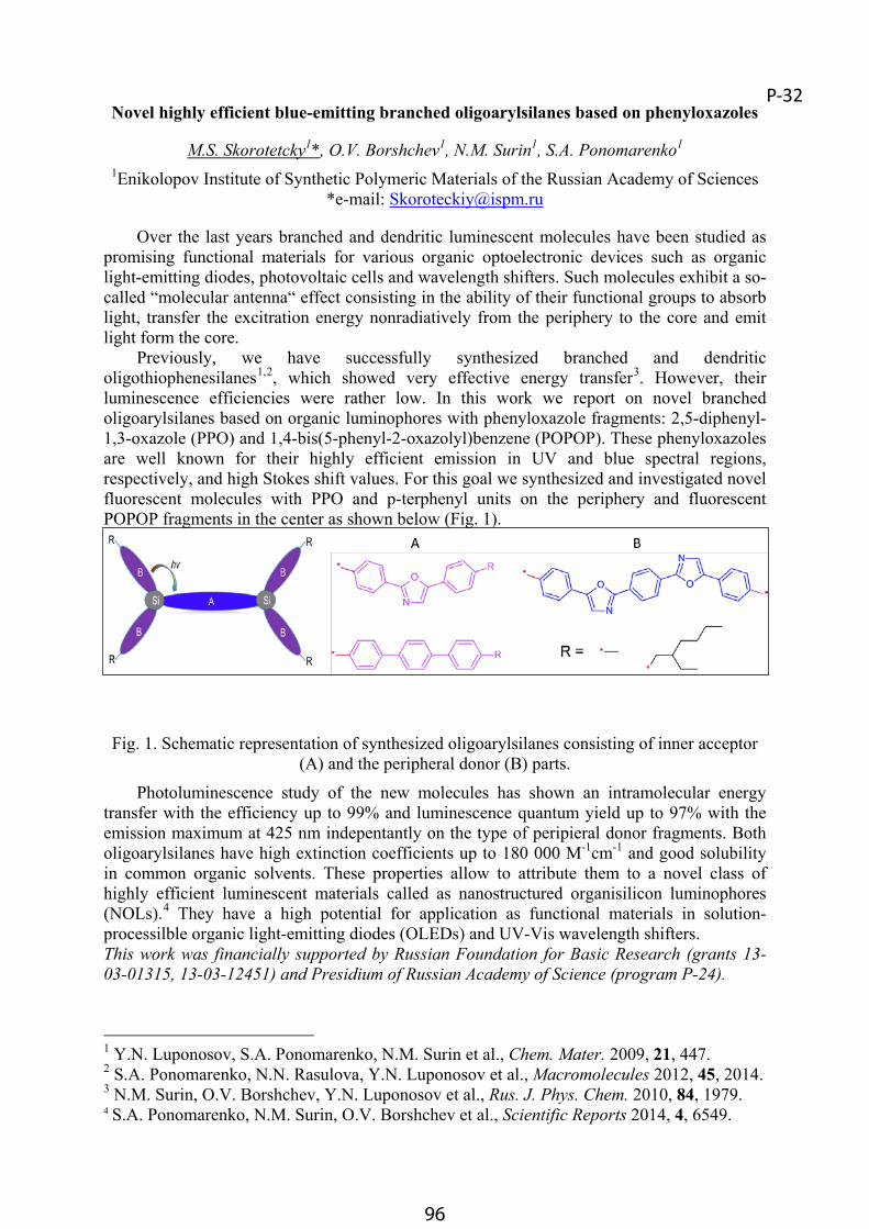
96
Novel highly efficient blue-emitting branched oligoarylsilanes based on phenyloxazoles
M.S. Skorotetcky1*, O.V. Borshchev1, N.M. Surin1, S.A. Ponomarenko1
1Enikolopov Institute of Synthetic Polymeric Materials of the Russian Academy of Sciences*e-mail: [email protected]
Over the last years branched and dendritic luminescent molecules have been studied as promising functional materials for various organic optoelectronic devices such as organic light-emitting diodes, photovoltaic cells and wavelength shifters. Such molecules exhibit a so-called “molecular antenna“ effect consisting in the ability of their functional groups to absorb light, transfer the excitration energy nonradiatively from the periphery to the core and emit light form the core.
Previously, we have successfully synthesized branched and dendritic oligothiophenesilanes1,2, which showed very effective energy transfer3. However, their luminescence efficiencies were rather low. In this work we report on novel branched oligoarylsilanes based on organic luminophores with phenyloxazole fragments: 2,5-diphenyl-1,3-oxazole (PPO) and 1,4-bis(5-phenyl-2-oxazolyl)benzene (POPOP). These phenyloxazoles are well known for their highly efficient emission in UV and blue spectral regions, respectively, and high Stokes shift values. For this goal we synthesized and investigated novel fluorescent molecules with PPO and p-terphenyl units on the periphery and fluorescent POPOP fragments in the center as shown below (Fig. 1).
Fig. 1. Schematic representation of synthesized oligoarylsilanes consisting of inner acceptor (A) and the peripheral donor (B) parts.
Photoluminescence study of the new molecules has shown an intramolecular energy transfer with the efficiency up to 99% and luminescence quantum yield up to 97% with the emission maximum at 425 nm indepentantly on the type of peripieral donor fragments. Both oligoarylsilanes have high extinction coefficients up to 180 000 M-1cm-1 and good solubility in common organic solvents. These properties allow to attribute them to a novel class of highly efficient luminescent materials called as nanostructured organisilicon luminophores (NOLs).4 They have a high potential for application as functional materials in solution-processilble organic light-emitting diodes (OLEDs) and UV-Vis wavelength shifters.This work was financially supported by Russian Foundation for Basic Research (grants 13-03-01315, 13-03-12451) and Presidium of Russian Academy of Science (program P-24).
1 Y.N. Luponosov, S.A. Ponomarenko, N.M. Surin et al., Chem. Mater. 2009, 21, 447.2 S.A. Ponomarenko, N.N. Rasulova, Y.N. Luponosov et al., Macromolecules 2012, 45, 2014.3 N.M. Surin, O.V. Borshchev, Y.N. Luponosov et al., Rus. J. Phys. Chem. 2010, 84, 1979. 4 S.A. Ponomarenko, N.M. Surin, O.V. Borshchev et al., Scientific Reports 2014, 4, 6549.
P-32

97
New star-shaped tris(2-methoxyphenyl)amine-based donor-acceptor oligomers for organic photovoltaics
A.N. Solodukhin1*, Y.N. Luponosov1, J. Min2, T. Ameri2, A.V. Bakirov1, M.S. Scherbina1, P.V. Dmitryakov1, S.N. Chvalun1, C.J. Brabec2, S.A. Ponomarenko1
1Institute of Synthetic Polymeric Materials RAS2Institute of Materials for Electronics and Energy Technology, Friedrich-Alexander-
University Erlangen-Nuremberg*e-mail: [email protected]
Thiophene-based organic semiconductors have been widely investigated as promising materials for organic electronics. Star-shaped and dendritic oligomers are very promising candidates among them1,2,3,4,5. In this work a series of novel star-shaped oligomers with tris(2-methoxyphenyl)amine donor core and bithiophene or terthiophene conjugated arms having dicyanovinyl acceptor substituents were synthesized and investigated (Figure 1).
S
S
S
NC
NC
SS
SNC
CN
S
SS
N
CNNC
O
OO
SS
HNC
CN
S
S
HCN
CN
S
S
N
H
CNNC
O
OO
SS
NC
CN
S
S
CN
CN
S
S
N
CNNC
O
OO
S
S
S
NC
NC
SS
SNC
CN
S
SS
N
CNNC
O
OO
N(Ph(OMe)-3T-DCV-Et)3
N(Ph(OMe)-2T-DCV)3 N(Ph(OMe)-2T-DCV-Me)3
N(Ph(OMe)-3T-DCV-Hex)3
Fig. 1. Chemical structures of the star-shaped oligomers synthesized and investigated.Synthesis of the star-shaped oligomers was based on a recently developed synthetic
approach using the Knövenagel condensation of the ketone precursor with malononitrile under a microwave irradiationi. The electrochemical, thermal and optical properties of these molecules were investigated by cyclic voltammetry, differential scanning calorimetry, thermogravimetric analysis and UV-Vis spectroscopy. They were applied as donor materials in solution processable bulk heterojunction organic photovoltaic devices. The best organic solar cell based on these star-shaped oligomers as a donor and PCBM[70] as an acceptor showed the open-circuit voltage of 0.88 V, the short-circuit current density of 9.15 mA/cm2,the fill factor of 54.4% and the power conversion efficiency of 4.38%.This work was supported by the Russian Scientific Foundation (project № 14-13-01380).
1 J. Min, Y. N. Luponosov, T. Ameri et al., Organic Electronics, 2013, 14, 219–229.2 Y.N. Luponosov, A.N. Solodukhin, S.A. Ponomarenko, Polymer Science, Ser. C, 2014, 56(1), 105–135.3 J. Min, Y.N. Luponosov, A. Gerl et al., Adv. Energy Mater., 2014, 4(5), 1301234.4 J. Min, Yu.N. Luponosov, A.N. Solodukhin et al., J. Mater. Chem. C, 2014, 36(2), 7614-7620.5 S.A. Ponomarenko, Y.N. Luponosov, J. Min et al., Faraday Discuss., 2014, 174, 313-339.
P-33Novel highly efficient blue-emitting branched oligoarylsilanes based on phenyloxazoles
M.S. Skorotetcky1*, O.V. Borshchev1, N.M. Surin1, S.A. Ponomarenko1
1Enikolopov Institute of Synthetic Polymeric Materials of the Russian Academy of Sciences*e-mail: [email protected]
Over the last years branched and dendritic luminescent molecules have been studied as promising functional materials for various organic optoelectronic devices such as organic light-emitting diodes, photovoltaic cells and wavelength shifters. Such molecules exhibit a so-called “molecular antenna“ effect consisting in the ability of their functional groups to absorb light, transfer the excitration energy nonradiatively from the periphery to the core and emit light form the core.
Previously, we have successfully synthesized branched and dendritic oligothiophenesilanes1,2, which showed very effective energy transfer3. However, their luminescence efficiencies were rather low. In this work we report on novel branched oligoarylsilanes based on organic luminophores with phenyloxazole fragments: 2,5-diphenyl-1,3-oxazole (PPO) and 1,4-bis(5-phenyl-2-oxazolyl)benzene (POPOP). These phenyloxazoles are well known for their highly efficient emission in UV and blue spectral regions, respectively, and high Stokes shift values. For this goal we synthesized and investigated novel fluorescent molecules with PPO and p-terphenyl units on the periphery and fluorescent POPOP fragments in the center as shown below (Fig. 1).
Fig. 1. Schematic representation of synthesized oligoarylsilanes consisting of inner acceptor (A) and the peripheral donor (B) parts.
Photoluminescence study of the new molecules has shown an intramolecular energy transfer with the efficiency up to 99% and luminescence quantum yield up to 97% with the emission maximum at 425 nm indepentantly on the type of peripieral donor fragments. Both oligoarylsilanes have high extinction coefficients up to 180 000 M-1cm-1 and good solubility in common organic solvents. These properties allow to attribute them to a novel class of highly efficient luminescent materials called as nanostructured organisilicon luminophores (NOLs).4 They have a high potential for application as functional materials in solution-processilble organic light-emitting diodes (OLEDs) and UV-Vis wavelength shifters.This work was financially supported by Russian Foundation for Basic Research (grants 13-03-01315, 13-03-12451) and Presidium of Russian Academy of Science (program P-24).
1 Y.N. Luponosov, S.A. Ponomarenko, N.M. Surin et al., Chem. Mater. 2009, 21, 447.2 S.A. Ponomarenko, N.N. Rasulova, Y.N. Luponosov et al., Macromolecules 2012, 45, 2014.3 N.M. Surin, O.V. Borshchev, Y.N. Luponosov et al., Rus. J. Phys. Chem. 2010, 84, 1979. 4 S.A. Ponomarenko, N.M. Surin, O.V. Borshchev et al., Scientific Reports 2014, 4, 6549.

98
Synthesis and Photophysical Properties of a Novel Cyan-Emitting Nanostructured Organosilicon Luminophore
T.Yu. Starikova1,2*, O.V. Borshchev2, N.M. Surin2, E.A. Svidchenko2, Y.V. Fedorov3,S.A.Ponomarenko2,4
1 Moscow State University, Department of Materials Science2 Enikolopov Institute of Synthetic Polymer Materials RAS
3 Nesmeyanov Institute of Organoelement Compounds RAS4 Moscow State University, Chemistry Department
*e-mail: [email protected]
Nanostructured Organosilicon Luminophores (NOLs) attract a vivid scientific and technological interest due to their unique optical properties, such as high quantum yields (QYs) combined with high molar extinction coefficients and short photoluminescence (PL) lifetimes1,2. NOL is a branched molecule which combines two different type luminophores with different band gaps connected to each other via silicon atoms. Thus, intramolecular Forster electron excitation energy transfer from the wider band gap luminophore (donor) to the narrower band gap luminophore (acceptor) is very efficient. Compared to inorganic quantum dots, organic NOLs are expected to exhibit lower toxicity and better compatibility with polymer matrices.
In this work, synthesis of the novel NOL containing six 5-hexyl-2,2’-bithyophene fragments per molecule and a central 1,4-bis(5-phenylthienyl-2)phenylene cyan-emitting fragment (Fig.1) was made by a multistep “bottom-up” approach. The donor part of the molecule was prepared via coupling of the organic lithium derivative of 5-hexyl-2,2’-bithiophene with (4-Br-phenyl)-trichlorosilane. The prepared precursor reacted with a bifunctional organoboronic derivative of 1,4-bis(2-thienyl)-benzene via Suzuki reaction to give the desired NOL. Its chemical structure was confirmed by a combination of GPC, NMR and MALDI-TOF techniques.
Fig.1. Chemical structure of the synthesized cyan-emitting NOL.
The NOL synthesized exhibits two absorption maxima at 337 nm and 380 nm with the molar extinction coefficient of 1.5×10⁵ L*mol/cm at 337 nm. Its PL spectrum has two maxima at 440 and 470 nm. An outstanding feature of this NOL is a very short luminescence lifetime of 0.8 ns combined with a very high luminescence QY of 94±6%. The estimated intramolecular energy transfer efficiency from the donor luminophores to the acceptor luminophore was found to be 97%. Due to these unique properties, the synthesized NOL is a promising material for high speed organic photonics.
This work was partially supported by RFBR (grant 13-03-01315).
1 S.A. Ponomarenko, N.M. Surin, O.V. Borshchev et. al. Sci. Rep. 2014, 4, 6549.2 M.S. Skorotetcky, O.V. Borshchev, N.M. Surin et al. Silicon 2015, 7, 191-200.
P-34
99
OFET transistors for logical circuit
S. Stritesky1*, M. Weiter1, M. Vala1, V. Simek2, A.Crha2, R. Ruzicka2
1 Brno University of Technology, Faculty of Chemistry, Material Research CentreBrno, Czech Republic
22Brno University of Technology, Faculty of Information Technology,Brno, Czech Republic
*e-mail: [email protected]
To date, a lot of publications were focused on increasing charge carrier mobility by synthesis of new organic semiconductors or suitable morphology of organic semiconductors in area of organic conducting channel. While progress in this area is significant, very little attention had been so far focused on integration of these materials into units and in particular to an electronic circuit due to the complexity of this problem.
This study is focused on organic field-effect transistors (OFETs), characterization of these transistors and identification of relevant parameters for logic circuit. Based on established parameters, simple logic circuits were designed. The main object of this study involves the preparation and characterization of OFETs which will be used in logical circuits. The obtained results will help to construction of more complex circuit with the prospect of industrial application.This work was supported by the Czech Science Foundation (project 13-29358S) and by the Ministry of Education Youth and Sports of the Czech Republic (project LO1211).
P-35Synthesis and Photophysical Properties of a Novel Cyan-Emitting Nanostructured
Organosilicon Luminophore
T.Yu. Starikova1,2*, O.V. Borshchev2, N.M. Surin2, E.A. Svidchenko2, Y.V. Fedorov3,S.A.Ponomarenko2,4
1 Moscow State University, Department of Materials Science2 Enikolopov Institute of Synthetic Polymer Materials RAS
3 Nesmeyanov Institute of Organoelement Compounds RAS4 Moscow State University, Chemistry Department
*e-mail: [email protected]
Nanostructured Organosilicon Luminophores (NOLs) attract a vivid scientific and technological interest due to their unique optical properties, such as high quantum yields (QYs) combined with high molar extinction coefficients and short photoluminescence (PL) lifetimes1,2. NOL is a branched molecule which combines two different type luminophores with different band gaps connected to each other via silicon atoms. Thus, intramolecular Forster electron excitation energy transfer from the wider band gap luminophore (donor) to the narrower band gap luminophore (acceptor) is very efficient. Compared to inorganic quantum dots, organic NOLs are expected to exhibit lower toxicity and better compatibility with polymer matrices.
In this work, synthesis of the novel NOL containing six 5-hexyl-2,2’-bithyophene fragments per molecule and a central 1,4-bis(5-phenylthienyl-2)phenylene cyan-emitting fragment (Fig.1) was made by a multistep “bottom-up” approach. The donor part of the molecule was prepared via coupling of the organic lithium derivative of 5-hexyl-2,2’-bithiophene with (4-Br-phenyl)-trichlorosilane. The prepared precursor reacted with a bifunctional organoboronic derivative of 1,4-bis(2-thienyl)-benzene via Suzuki reaction to give the desired NOL. Its chemical structure was confirmed by a combination of GPC, NMR and MALDI-TOF techniques.
Fig.1. Chemical structure of the synthesized cyan-emitting NOL.
The NOL synthesized exhibits two absorption maxima at 337 nm and 380 nm with the molar extinction coefficient of 1.5×10⁵ L*mol/cm at 337 nm. Its PL spectrum has two maxima at 440 and 470 nm. An outstanding feature of this NOL is a very short luminescence lifetime of 0.8 ns combined with a very high luminescence QY of 94±6%. The estimated intramolecular energy transfer efficiency from the donor luminophores to the acceptor luminophore was found to be 97%. Due to these unique properties, the synthesized NOL is a promising material for high speed organic photonics.
This work was partially supported by RFBR (grant 13-03-01315).
1 S.A. Ponomarenko, N.M. Surin, O.V. Borshchev et. al. Sci. Rep. 2014, 4, 6549.2 M.S. Skorotetcky, O.V. Borshchev, N.M. Surin et al. Silicon 2015, 7, 191-200.
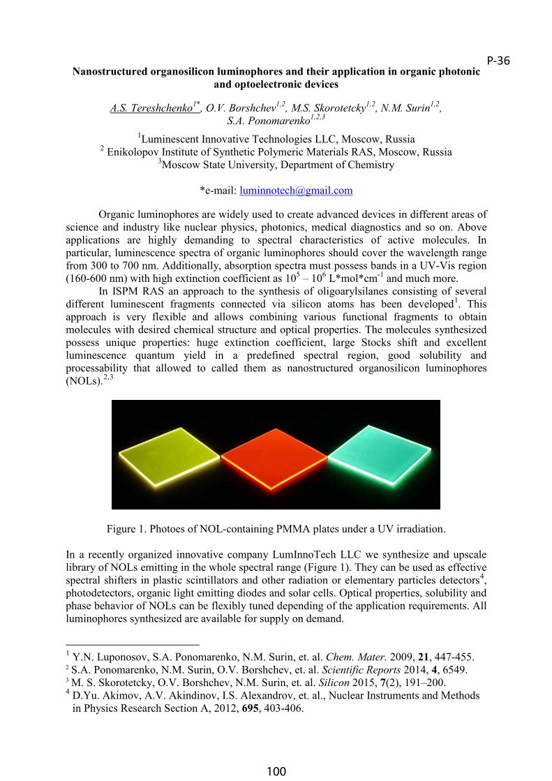
100
Nanostructured organosilicon luminophores and their application in organic photonicand optoelectronic devices
A.S. Tereshchenko1*, O.V. Borshchev1,2, M.S. Skorotetcky1,2, N.M. Surin1,2,S.A. Ponomarenko1,2,3
1Luminescent Innovative Technologies LLC, Moscow, Russia2 Enikolopov Institute of Synthetic Polymeric Materials RAS, Moscow, Russia
3Moscow State University, Department of Chemistry
*e-mail: [email protected]
Organic luminophores are widely used to create advanced devices in different areas of science and industry like nuclear physics, photonics, medical diagnostics and so on. Above applications are highly demanding to spectral characteristics of active molecules. In particular, luminescence spectra of organic luminophores should cover the wavelength range from 300 to 700 nm. Additionally, absorption spectra must possess bands in a UV-Vis region (160-600 nm) with high extinction coefficient as 105 – 106 L*mol*cm-1 and much more.
In ISPM RAS an approach to the synthesis of oligoarylsilanes consisting of several different luminescent fragments connected via silicon atoms has been developed1. This approach is very flexible and allows combining various functional fragments to obtain molecules with desired chemical structure and optical properties. The molecules synthesized possess unique properties: huge extinction coefficient, large Stocks shift and excellent luminescence quantum yield in a predefined spectral region, good solubility and processability that allowed to called them as nanostructured organosilicon luminophores (NOLs).2,3
Figure 1. Photoes of NOL-containing PMMA plates under a UV irradiation.
In a recently organized innovative company LumInnoTech LLC we synthesize and upscale library of NOLs emitting in the whole spectral range (Figure 1). They can be used as effective spectral shifters in plastic scintillators and other radiation or elementary particles detectors4,photodetectors, organic light emitting diodes and solar cells. Optical properties, solubility and phase behavior of NOLs can be flexibly tuned depending of the application requirements. All luminophores synthesized are available for supply on demand.
1 Y.N. Luponosov, S.A. Ponomarenko, N.M. Surin, et. al. Chem. Mater. 2009, 21, 447-455.2 S.A. Ponomarenko, N.M. Surin, O.V. Borshchev, et. al. Scientific Reports 2014, 4, 6549.3 M. S. Skorotetcky, O.V. Borshchev, N.M. Surin, et. al. Silicon 2015, 7(2), 191–200.4 D.Yu. Akimov, A.V. Akindinov, I.S. Alexandrov, et. al., Nuclear Instruments and Methods
in Physics Research Section A, 2012, 695, 403-406.
P-36
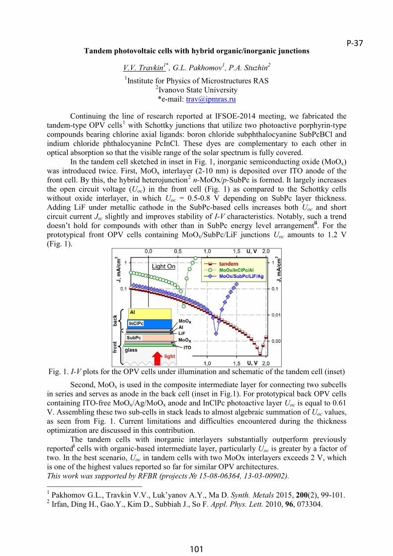
101
Tandem photovoltaic cells with hybrid organic/inorganic junctions
V.V. Travkin1*, G.L. Pakhomov1, P.A. Stuzhin2
1Institute for Physics of Microstructures RAS2Ivanovo State University*e-mail: [email protected]
Continuing the line of research reported at IFSOE-2014 meeting, we fabricated the tandem-type OPV cells1 with Schottky junctions that utilize two photoactive porphyrin-type compounds bearing chlorine axial ligands: boron chloride subphthalocyanine SubPcBCl and indium chloride phthalocyanine PcInCl. These dyes are complementary to each other in optical absorption so that the visible range of the solar spectrum is fully covered.
In the tandem cell sketched in inset in Fig. 1, inorganic semiconducting oxide (MoOx)was introduced twice. First, MoOx interlayer (2-10 nm) is deposited over ITO anode of the front cell. By this, the hybrid heterojunction2 n-MoOx/p-SubPc is formed. It largely increasesthe open circuit voltage (Uoc) in the front cell (Fig. 1) as compared to the Schottky cells without oxide interlayer, in which Uoc = 0.5-0.8 V depending on SubPc layer thickness.Adding LiF under metallic cathode in the SubPc-based cells increases both Uoc and short circuit current Jsc slightly and improves stability of I-V characteristics. Notably, such a trend doesn’t hold for compounds with other than in SubPc energy level arrangementii. For the prototypical front OPV cells containing MoOx/SubPc/LiF junctions Uoc amounts to 1.2 V(Fig. 1).
Fig. 1. I-V plots for the OPV cells under illumination and schematic of the tandem cell (inset) Second, MoOx is used in the composite intermediate layer for connecting two subcells
in series and serves as anode in the back cell (inset in Fig.1). For prototypical back OPV cells containing ITO-free MoOx/Ag/MoOx anode and InClPc photoactive layer Uoc is equal to 0.61V. Assembling these two sub-cells in stack leads to almost algebraic summation of Uoc values, as seen from Fig. 1. Current limitations and difficulties encountered during the thickness optimization are discussed in this contribution.
The tandem cells with inorganic interlayers substantially outperform previously reportedi cells with organic-based intermediate layer, particularly Uoc is greater by a factor of two. In the best scenario, Uoc in tandem cells with two MoOx interlayers exceeds 2 V, which is one of the highest values reported so far for similar OPV architectures.This work was supported by RFBR (projects № 15-08-06364, 13-03-00902).
1 Pakhomov G.L., Travkin V.V., Luk’yanov A.Y., Ma D. Synth. Metals 2015, 200(2), 99-101.2 Irfan, Ding H., Gao.Y., Kim D., Subbiah J., So F. Appl. Phys. Lett. 2010, 96, 073304.
P-37Nanostructured organosilicon luminophores and their application in organic photonic
and optoelectronic devices
A.S. Tereshchenko1*, O.V. Borshchev1,2, M.S. Skorotetcky1,2, N.M. Surin1,2,S.A. Ponomarenko1,2,3
1Luminescent Innovative Technologies LLC, Moscow, Russia2 Enikolopov Institute of Synthetic Polymeric Materials RAS, Moscow, Russia
3Moscow State University, Department of Chemistry
*e-mail: [email protected]
Organic luminophores are widely used to create advanced devices in different areas of science and industry like nuclear physics, photonics, medical diagnostics and so on. Above applications are highly demanding to spectral characteristics of active molecules. In particular, luminescence spectra of organic luminophores should cover the wavelength range from 300 to 700 nm. Additionally, absorption spectra must possess bands in a UV-Vis region (160-600 nm) with high extinction coefficient as 105 – 106 L*mol*cm-1 and much more.
In ISPM RAS an approach to the synthesis of oligoarylsilanes consisting of several different luminescent fragments connected via silicon atoms has been developed1. This approach is very flexible and allows combining various functional fragments to obtain molecules with desired chemical structure and optical properties. The molecules synthesized possess unique properties: huge extinction coefficient, large Stocks shift and excellent luminescence quantum yield in a predefined spectral region, good solubility and processability that allowed to called them as nanostructured organosilicon luminophores (NOLs).2,3
Figure 1. Photoes of NOL-containing PMMA plates under a UV irradiation.
In a recently organized innovative company LumInnoTech LLC we synthesize and upscale library of NOLs emitting in the whole spectral range (Figure 1). They can be used as effective spectral shifters in plastic scintillators and other radiation or elementary particles detectors4,photodetectors, organic light emitting diodes and solar cells. Optical properties, solubility and phase behavior of NOLs can be flexibly tuned depending of the application requirements. All luminophores synthesized are available for supply on demand.
1 Y.N. Luponosov, S.A. Ponomarenko, N.M. Surin, et. al. Chem. Mater. 2009, 21, 447-455.2 S.A. Ponomarenko, N.M. Surin, O.V. Borshchev, et. al. Scientific Reports 2014, 4, 6549.3 M. S. Skorotetcky, O.V. Borshchev, N.M. Surin, et. al. Silicon 2015, 7(2), 191–200.4 D.Yu. Akimov, A.V. Akindinov, I.S. Alexandrov, et. al., Nuclear Instruments and Methods
in Physics Research Section A, 2012, 695, 403-406.
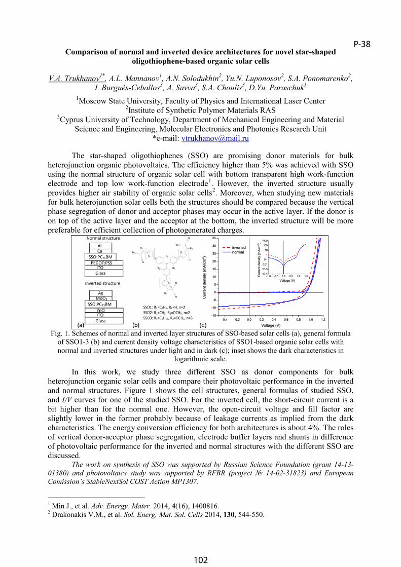
102
Comparison of normal and inverted device architectures for novel star-shaped oligothiophene-based organic solar cells
V.A. Trukhanov1*, A.L. Mannanov1, A.N. Solodukhin2, Yu.N. Luponosov2, S.A. Ponomarenko2,I. Burgués-Ceballos3, A. Savva3, S.A. Choulis3, D.Yu. Paraschuk1
1Moscow State University, Faculty of Physics and International Laser Center 2Institute of Synthetic Polymer Materials RAS
3Cyprus University of Technology, Department of Mechanical Engineering and Material Science and Engineering, Molecular Electronics and Photonics Research Unit
*e-mail: [email protected]
The star-shaped oligothiophenes (SSO) are promising donor materials for bulk heterojunction organic photovoltaics. The efficiency higher than 5% was achieved with SSOusing the normal structure of organic solar cell with bottom transparent high work-function electrode and top low work-function electrode1. However, the inverted structure usually provides higher air stability of organic solar cells2. Moreover, when studying new materials for bulk heterojunction solar cells both the structures should be compared because the vertical phase segregation of donor and acceptor phases may occur in the active layer. If the donor is on top of the active layer and the acceptor at the bottom, the inverted structure will be more preferable for efficient collection of photogenerated charges.
Fig. 1. Schemes of normal and inverted layer structures of SSO-based solar cells (a), general formula of SSO1-3 (b) and current density voltage characteristics of SSO1-based organic solar cells with normal and inverted structures under light and in dark (c); inset shows the dark characteristics in
logarithmic scale.
In this work, we study three different SSO as donor components for bulk heterojunction organic solar cells and compare their photovoltaic performance in the inverted and normal structures. Figure 1 shows the cell structures, general formulas of studied SSO,and I/V curves for one of the studied SSO. For the inverted cell, the short-circuit current is abit higher than for the normal one. However, the open-circuit voltage and fill factor are slightly lower in the former probably because of leakage currents as implied from the dark characteristics. The energy conversion efficiency for both architectures is about 4%. The roles of vertical donor-acceptor phase segregation, electrode buffer layers and shunts in difference of photovoltaic performance for the inverted and normal structures with the different SSO are discussed.
The work on synthesis of SSO was supported by Russian Science Foundation (grant 14-13-01380) and photovoltaics study was supported by RFBR (project № 14-02-31823) and European Comission’s StableNextSol COST Action MP1307.
1 Min J., et al. Adv. Energy. Mater. 2014, 4(16), 1400816.2 Drakonakis V.M., et al. Sol. Energ. Mat. Sol. Cells 2014, 130, 544-550.
P-38

103
Disiloxane derivatives of BTBT for monolayer organic field-effect transistors
A.A. Trul1*, E.V. Agina1, A.S. Sizov1, O.V. Borshchev1, S.A. Ponomarenko1,2
1Institute of Synthetic Polymer Materials RAS2Moscow State University, Department of Chemistry
*e-mail: [email protected]
The most part of organic electronic devices are based on organic field-effect transistors (OFETs). Since charge transport mainly takes place in a few nanometers thick layer of organic semiconductor1, formation of monolayer OFETs allows to save significant amount of rather expensive organic semiconducting materials decreasing costs of target devices without losing its functionality in OFETs. Thus, usage of monolayer OFETs is one ofthe perspective ways in organic electronics. It was shown that [1]benzothieno[3,2-b][1]-benzothiophene (BTBT) derivatives have high potential for OFETs due to its high charge carrier mobility (up to 43 cm2/Vs in thick OFETs2).
Here we adopted spin-coating, Langmuir-Blodgett (LB) and Langmuir-Schaefer (LS)techniques for the fabrication of BTBT-based monolayer OFETs. Disiloxane disubstitutedderivative of BTBT – 1,3-bis[11-(7-hexyl[1]benzothieno[3,2-b][1]benzothien-2-yl)undecyl]-1,1,3,3-tetramethyldisiloxane, O-(Si-Und-BTBT-Hex)2, which is stable under normal atmospheric conditions, has been used as an active layer in these OFETs. Figure 1demonstrates output (a) and transfer (b) characteristics of OFETs with 30 µm channel length.Such behavior is typical for p- type devices.
Figure 1. Output (a) and transfer (b) characteristics of OTFTs with 30 µm channel length.
The OFETs show hole mobility up to 0.04 cm2/(V s) for spin-coating devices and up to 0.002 cm2/(V s) for LB and LS devices. The obtained on/off current ratio were up to 106 (SC devices) and up to 104 (LB and LS devices). These OFETs were found to be stable after half-year storage under ambient conditions that enables using this organic semiconducting compound for large-area electronics fabrication.
This work was supported by RFBR (project № 14-03-00873) and Russian Academy of Sciences (program OKh-3).
1 Dinelli, F.; Murgia, M.; Levy, P.; Cavallini, M.; Biscarini, F.; de Leeuw, D.M. Phys. Rev.Lett. 2004, 92, 116802.2 Yuan, Y., et al., Nature Commun. 5:3005 (2014).
-50 -45 -40 -35 -30 -25 -20 -15 -10 -5 0 5-6E-7
-5E-7
-4E-7
-3E-7
-2E-7
-1E-7
0
1E-7
Vg=-40V
Vg=-30V
Dra
in c
urr
ent, A
Drain voltage, V
Vg=-20V
-45 -40 -35 -30 -25 -20 -15 -10 -5 0 5 10
1E-11
1E-10
1E-9
1E-8
1E-7
1E-6
1E-5
-D
rain
curr
ent,
Gate voltage,
0.0
5.0E-7
1.0E-6
1.5E-6
2.0E-6
2.5E-6
3.0E-6
3.5E-6
4.0E-6
-D
rain
curr
ant,
Vd=-20V
(a) (b)
P-39Comparison of normal and inverted device architectures for novel star-shaped
oligothiophene-based organic solar cells
V.A. Trukhanov1*, A.L. Mannanov1, A.N. Solodukhin2, Yu.N. Luponosov2, S.A. Ponomarenko2,I. Burgués-Ceballos3, A. Savva3, S.A. Choulis3, D.Yu. Paraschuk1
1Moscow State University, Faculty of Physics and International Laser Center 2Institute of Synthetic Polymer Materials RAS
3Cyprus University of Technology, Department of Mechanical Engineering and Material Science and Engineering, Molecular Electronics and Photonics Research Unit
*e-mail: [email protected]
The star-shaped oligothiophenes (SSO) are promising donor materials for bulk heterojunction organic photovoltaics. The efficiency higher than 5% was achieved with SSOusing the normal structure of organic solar cell with bottom transparent high work-function electrode and top low work-function electrode1. However, the inverted structure usually provides higher air stability of organic solar cells2. Moreover, when studying new materials for bulk heterojunction solar cells both the structures should be compared because the vertical phase segregation of donor and acceptor phases may occur in the active layer. If the donor is on top of the active layer and the acceptor at the bottom, the inverted structure will be more preferable for efficient collection of photogenerated charges.
Fig. 1. Schemes of normal and inverted layer structures of SSO-based solar cells (a), general formula of SSO1-3 (b) and current density voltage characteristics of SSO1-based organic solar cells with normal and inverted structures under light and in dark (c); inset shows the dark characteristics in
logarithmic scale.
In this work, we study three different SSO as donor components for bulk heterojunction organic solar cells and compare their photovoltaic performance in the inverted and normal structures. Figure 1 shows the cell structures, general formulas of studied SSO,and I/V curves for one of the studied SSO. For the inverted cell, the short-circuit current is abit higher than for the normal one. However, the open-circuit voltage and fill factor are slightly lower in the former probably because of leakage currents as implied from the dark characteristics. The energy conversion efficiency for both architectures is about 4%. The roles of vertical donor-acceptor phase segregation, electrode buffer layers and shunts in difference of photovoltaic performance for the inverted and normal structures with the different SSO are discussed.
The work on synthesis of SSO was supported by Russian Science Foundation (grant 14-13-01380) and photovoltaics study was supported by RFBR (project № 14-02-31823) and European Comission’s StableNextSol COST Action MP1307.
1 Min J., et al. Adv. Energy. Mater. 2014, 4(16), 1400816.2 Drakonakis V.M., et al. Sol. Energ. Mat. Sol. Cells 2014, 130, 544-550.

104
Water-dispersible carbon nanotubes / polyaniline composites with improved electrical conductivity
P.I. Turkina*, A.V. Kubarkov, O.A. Pyshkina, V.G. SergeyevMoscow State University, Department of Chemistry
*e-mail: [email protected]
In recent years, composites of carbon nanotubes with polyaniline (PANI) attract considerable attention because of their high electrical conductivity, electrochemical activity and capacity, making them promising for applications in electronic devices, supercapacitors and electrochemical sensors. Preparation, processing and application of such composites is complicated due to insolubility of both nanotubes and polyaniline in all common solvents caused by their strong tendency to self-aggregation.
In the present work water-dispersible carbon nanotubes / PANI composites of uniform structure were prepared. Multi-walled carbon nanotubes were previously functionalized with sulfophenyl groups via diazotation reaction to obtain sulfonated nanotubes (sNT) with high dispersibility in aqueous medium up to 1 mg/mL. Oxidative chemical polymerization of aniline was then carried out in sNT aqueous dispersions. As a result, uniform PANI layers were formed at the nanotubes surfaces. The presence of sulfonic groups provided the dispersibility of PANI/sNT complexes. Mechanically stable free-standing composite films were cast from prepared PANI/sNT dispersions. Electrical conductivity of sNT/PANI films was found to be several times higher than that of both sNT and PANI individual components.Electrochemical properties of the composites were studied by cyclic voltammetry.
This work was supported by RFBR (project № 14-03-31332).
P-40

105
1,8-diazabenzopyrenes and 1,7-diazaperylenes: synthesys and characterization as electron donor and acceptor molecules
M.N. Uvarov1*, D.S. Baranov1,2, A.G. Popov1,2, M.S. Kazantsev3, E.A. Mostovich3,E.M. Glebov1,2, L.V. Kulik1,2
1Voevodsky Institute of Chemical Kinetics and Combustion SB RAS2Novosibirsk State University
3Vorozhtsov Institute of Organic Chemistry SB RAS*e-mail: [email protected]
Novel organic donor-acceptor systems with π-conjugated parts are promising for photovoltaic applications. The aim of this work is to obtain new molecules with condensed heterocycles and understanding their capability as organic semiconductor material in photovoltaic devices. The synthesized derivatives of 1,8-diazabenzopyrene1 and 1,7-diazaperylene2 with different substitutes R (Fig.1) were characterized by cyclic voltammetry (CVA), UV-vis and luminescence spectroscopies.
Fig.1. The derivatives of 1,8-diazabenzopyrene (A) and 1,7-diazaperylene (B).For the substances investigated the HOMO-LUMO gap was determined in the range of 1,7 –2,7 eV both by CVA technique and from UV-vis spectra edges. Photoinduced electron transfer in composites consisting of the compound a with MEH-PPV (Poly[2-methoxy-5-(2-ethylhexyloxy)-1,4-phenylenevinylene]), and b with P3HT (Poly(3-hexylthiophene-2,5-diyl)) produced two lines in light-induced EPR spectra. Two light-induced EPR lines were obtained for the composites of c:P3HT and c:PCBM ([6,6]-Phenyl C61 butyric acid methyl ester), where the substance c could be electron donor or acceptor. These EPR lines were attributed to the radicals c-:P3HT+ and c+:PCBM- for the corresponding composites. This work was supported by RFBR (projects № 14-03-31183, № 15-33-20421).
1 Baranov D.S., Popov A.G., Uvarov M.N., et al. Synth. Met. 2015, 201, 43–48.2 Baranov D.S., Popov A.G., Uvarov M.N., Kulik L.V. Mendeleev Commun. 2014, 24, 383-385.
P-41Water-dispersible carbon nanotubes / polyaniline composites with improved electrical
conductivity
P.I. Turkina*, A.V. Kubarkov, O.A. Pyshkina, V.G. SergeyevMoscow State University, Department of Chemistry
*e-mail: [email protected]
In recent years, composites of carbon nanotubes with polyaniline (PANI) attract considerable attention because of their high electrical conductivity, electrochemical activity and capacity, making them promising for applications in electronic devices, supercapacitors and electrochemical sensors. Preparation, processing and application of such composites is complicated due to insolubility of both nanotubes and polyaniline in all common solvents caused by their strong tendency to self-aggregation.
In the present work water-dispersible carbon nanotubes / PANI composites of uniform structure were prepared. Multi-walled carbon nanotubes were previously functionalized with sulfophenyl groups via diazotation reaction to obtain sulfonated nanotubes (sNT) with high dispersibility in aqueous medium up to 1 mg/mL. Oxidative chemical polymerization of aniline was then carried out in sNT aqueous dispersions. As a result, uniform PANI layers were formed at the nanotubes surfaces. The presence of sulfonic groups provided the dispersibility of PANI/sNT complexes. Mechanically stable free-standing composite films were cast from prepared PANI/sNT dispersions. Electrical conductivity of sNT/PANI films was found to be several times higher than that of both sNT and PANI individual components.Electrochemical properties of the composites were studied by cyclic voltammetry.
This work was supported by RFBR (project № 14-03-31332).
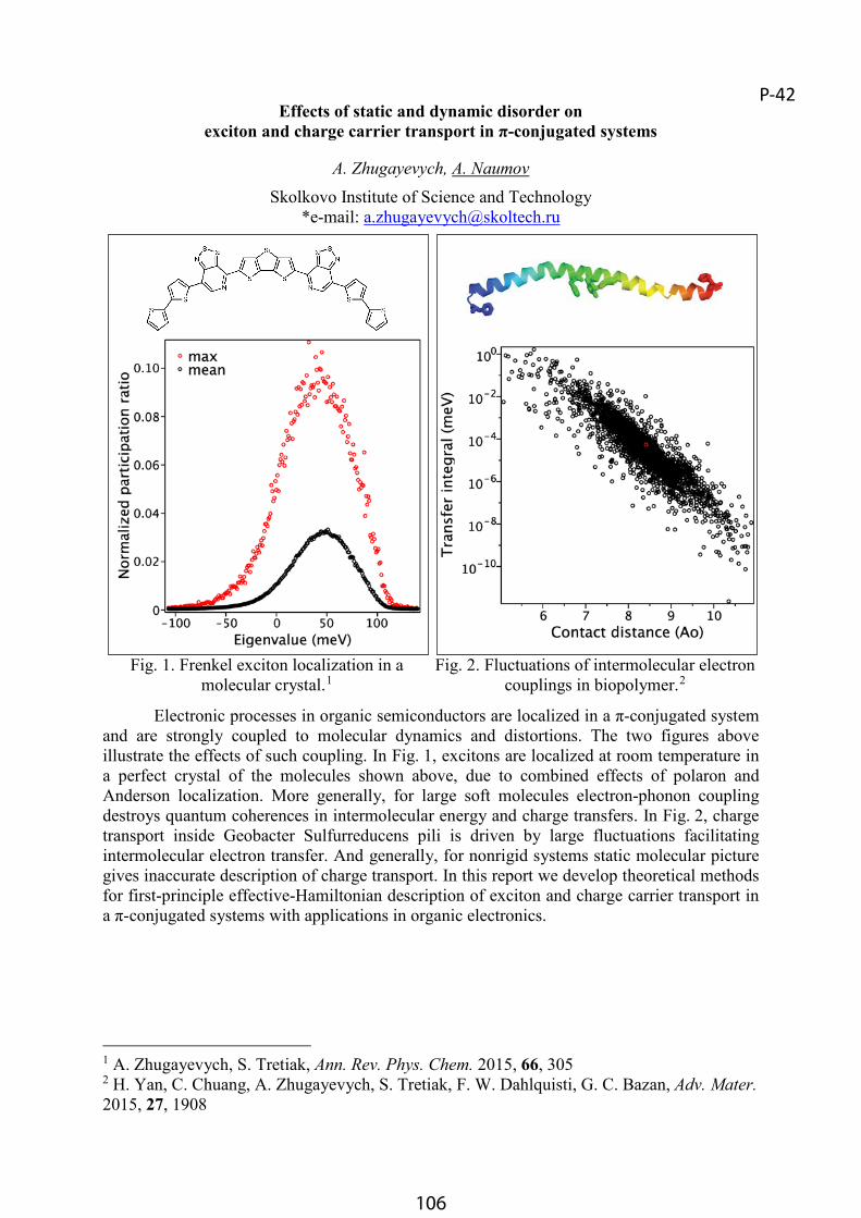
106
Effects of static and dynamic disorder onexciton and charge carrier transport in π-conjugated systems
A. Zhugayevych, A. NaumovSkolkovo Institute of Science and Technology
*e-mail: [email protected]
Fig. 1. Frenkel exciton localization in a molecular crystal.1
Fig. 2. Fluctuations of intermolecular electron couplings in biopolymer.2
Electronic processes in organic semiconductors are localized in a π-conjugated systemand are strongly coupled to molecular dynamics and distortions. The two figures above illustrate the effects of such coupling. In Fig. 1, excitons are localized at room temperature in a perfect crystal of the molecules shown above, due to combined effects of polaron and Anderson localization. More generally, for large soft molecules electron-phonon coupling destroys quantum coherences in intermolecular energy and charge transfers. In Fig. 2, charge transport inside Geobacter Sulfurreducens pili is driven by large fluctuations facilitating intermolecular electron transfer. And generally, for nonrigid systems static molecular picture gives inaccurate description of charge transport. In this report we develop theoretical methods for first-principle effective-Hamiltonian description of exciton and charge carrier transport in a π-conjugated systems with applications in organic electronics.
1 A. Zhugayevych, S. Tretiak, Ann. Rev. Phys. Chem. 2015, 66, 3052 H. Yan, C. Chuang, A. Zhugayevych, S. Tretiak, F. W. Dahlquisti, G. C. Bazan, Adv. Mater.2015, 27, 1908
P-42

107
Effect of sample size on photoluminescence of crystalline thiophene-phenylene co-oligomers
V.G. Konstantinov1*, L.G. Kudryashova1, O.V. Borshchev2, S.A. Ponomarenko2,3,D.Y. Paraschuk1,
1Physics Department and International Laser Center,Moscow State University, Moscow, Russia
2Institute of Synthetic Polymeric Materials of Russian Academy of Sciences, Moscow, Russia3Chemistry Department, Moscow State University, Moscow, Russia
*e-mail: [email protected]
Single crystals of thiophene-phenylene co-oligomers (TPCO) are promising materials for organic optoelectronics as they demonstrate high photoluminescence (PL) efficiency andcharge carrier mobilities. PL external quantum yield (QY) of TPCO was found to be about 60 %1, and charge mobilities in the range 0.1–1.0 cm2/(V·s) were reported2.
In this work, we investigate PL and its QY in two similar types of solution-grown TPCOsingle crystals: 5,5'-bis(4-(trimethylsilyl)phenyl)-2,2'-bithiophene (TMS-PTTP-TMS) and5,5'-bis(4-(trifluoromethyl)phenyl)-2,2'-bithiophene (CF3-PTTP-CF3). The single crystalline TPCO films have sizes of 1-3 mm with thickness of some um. In the studied crystals, PL reabsorption is noticeable due to absorption and emission spectra overlap. To avoid reabsorption and increase PL QY, we milled the single crystals. Fig. 1 demonstrates PL spectra and PL QY of single crystals and their milled samples. It is seen that milling decreases the reabsorption effect. However, we found that the larger CF3-PTTP-CF3 films show lower PL QY, whereas the larger TMS-PTTP-TMS demonstrates higher PL QY. The possiblereasons of different PL features of the two types of TPCO crystals are discussed.
Fig. 1. PL spectra of TMS-PTTP-TMS and CF3-PTTP-CF3 single crystals (black) and milled samples (red)
1 Hong-Hua Fang et al. Adv. Funct. Mater. 2012, 22, 33–38.2 Hotta S., Yamao T. J. Mater. Chem., 2011, 21, 1295-1304.
TMS-PTTP-TMS CF3-PTTP-CF3
P-43Effects of static and dynamic disorder on
exciton and charge carrier transport in π-conjugated systems
A. Zhugayevych, A. NaumovSkolkovo Institute of Science and Technology
*e-mail: [email protected]
Fig. 1. Frenkel exciton localization in a molecular crystal.1
Fig. 2. Fluctuations of intermolecular electron couplings in biopolymer.2
Electronic processes in organic semiconductors are localized in a π-conjugated systemand are strongly coupled to molecular dynamics and distortions. The two figures above illustrate the effects of such coupling. In Fig. 1, excitons are localized at room temperature in a perfect crystal of the molecules shown above, due to combined effects of polaron and Anderson localization. More generally, for large soft molecules electron-phonon coupling destroys quantum coherences in intermolecular energy and charge transfers. In Fig. 2, charge transport inside Geobacter Sulfurreducens pili is driven by large fluctuations facilitating intermolecular electron transfer. And generally, for nonrigid systems static molecular picture gives inaccurate description of charge transport. In this report we develop theoretical methods for first-principle effective-Hamiltonian description of exciton and charge carrier transport in a π-conjugated systems with applications in organic electronics.
1 A. Zhugayevych, S. Tretiak, Ann. Rev. Phys. Chem. 2015, 66, 3052 H. Yan, C. Chuang, A. Zhugayevych, S. Tretiak, F. W. Dahlquisti, G. C. Bazan, Adv. Mater.2015, 27, 1908

108
Photovoltaic performance of some conventional and innovative fullerene- and polymer-based photoactive materials
A.V. Mumyatov1,2*, A.V. Akkuratov1,2, I. E. Kuznetsov1,2, F. A. Prudnov1, D. K. Susarova1
1 Institute for Problems of Chemical Physics of Russian Academy of Sciences2 FOMaterials LTD
*e-mail: [email protected]
Institute for Problems of Chemical Physics of Russian Academy of Sciences (IPCP RAS) was involved in the development of organic bulk heterojunction solar cells since early 2000s. A number of novel fullerene derivatives and conjugated polymers were designed for highly efficient and stable organic photovoltaics (OPV). The accumulated scientific knowledge and expertise were reflected in a number of high-level publications and patents. In particular, it was shown that reliable performances of organic solar cells can be achieved only via a severe quality control of all employed organic semiconductor materials using the most sensitive analytical techniques (e.g. special ESR or impedance methods developed at IPCP RAS1-3).
IPCP RAS has launched recently a spin-off company FOMaterials LTD with the aim to provide high-quality fullerene- and polymer-based materials to the Russian and international research groups working in the field of organic electronics and, in particular, OPV. In this presentation we will discuss recent results of the collaborative research performed at FOMaterials LTD company and IPCP RAS and directed towards large-scale preparation of conventional (e.g. PCDTBT, F8TBT, PCBM, ICBA) and a number of innovative polymers and fullerene derivatives. In particular, we will present the data on photovoltaic performance of our materials in standard and inverted device geometries.
1 D. K. Susarova, N. P. Piven, A. V. Akkuratov, L. F. Frolova, M. S. Polinskaya, S. A.Ponomarenko, S. D. Babenko, P. A. Troshin, ESR spectroscopy as a powerful technique forprobing the quality of conjugated polymers designed for photovoltaic applications. Chem. Comm., 2015, 51, 2239-22412 L. A. Frolova, N. P. Piven, D. K. Susarova, A. V. Akkuratov, S. D. Babenko, P.A. Troshin. ESR spectroscopy for monitoring photochemical and thermal degradation of conjugated polymers used as electron donor materials in organic bulk heterojunction solar cells. Chem. Comm., 2015, 51, 2242-22443 P. A. Troshin, D. K. Susarova, Y. L. Moskvin, I. E. Kuznetsov, S. A. Ponomarenko, E. N. Myshkovskaya, K. A. Zakharcheva, A. A. Balakai, S. D. Babenko, V. F. Razumov. A simple approach to control the quality of conjugated polymers designed for photovoltaic applications. Adv. Funct. Mater. 2010, 20, 4351–4357
P-44

109
Effects of donor and acceptor units on physical and photovoltaic properties of D-Aoligomers
D.A. Khanin1*, Y.N. Luponosov1, J. Min2, T. Ameri2, P.V. Dmitryakov3, Obrezkova M.A.,1S.M. Peregudova1, F.V. Drozdov1, N.M. Surin, C.J. Brabec2, S.A. Ponomarenko1
1Institute of Synthetic Polymeric Materials RAS2Institute of Materials for Electronics and Energy Technology, Friedrich-Alexander-
University Erlangen-Nuremberg3Scientific and Research Centre Kurchatov Institute
*e-mail: [email protected]
Organic solar cell technology is a promising candidate for the solar energy conversion compared to its inorganic counterparts due to its low cost, light weight, and potential use in flexible devices. Small molecules are one of the most interesting candidates for these purposes. In this work, a library of new oligomers (see Figure 1), where benzodithiophene, dithienosilole1 or dithienopyrrole donor central units linked through bithiophene π-bridges with various acceptor units, such as dicyanovinyl, alkyl-rhodanine or alkyldicyanovinylsubstitutes, were synthesized. The electrochemical, thermal and optical properties of these molecules were investigated by cyclic voltammetry, differential scanning calorimetry, thermogravimetric analysis and UV-Vis spectroscopy. These oligomers exhibit interesting optical and promising photovoltaic properties that are highly dependent on the type of central donor and terminal acceptor units as well as the length of alkyl groups.2,3.
SSR Ar S
SR
S S
N
C8H17H17C8
S S
Si
C8H17H17C8
S
S
O-C8H17
O-C8H17
S S
Si
C10H21H21C10
* Me
CNNC
SN
S
O
*
SN
S
O
*
*
CNNC
HNALK
** R =
;
Ar =
;
;
;
;
Fig. 1. Schematic structures of the linear D-A oligomersThis work was supported by RFBR (№15-33-20957). Synthesis and characterization of oligomers with alkyl-rhodanine groups was supported by Program of President of Russian Federation (МК-5061.2015.3).
1 Yuriy N. Luponosov, Jie Min, Tayebeh Ameri, Christoph J. Brabec, Sergei A. Ponomarenko Organic Electronics 2014, 15, 3800.2 Luponosov, Y. N., Min, J., Bakirov, A.V., Dmitryakov, P.V., Chvalun, S. N., Peregudova, S. M., Ameri, T., Brabec, C. J., Ponomarenko, S. A., “Dyes and Pigments,” (2015), 122, 213-223.3 Min, J., Luponosov, Y. N., Gasparini, N., Richter, M., Bakirov, A. V., Shcherbina, M. A., Chvalun, S. N., Grodd, L., Grigorian, S., Ameri, T., Ponomarenko, S. A., Brabec, C. J. (2015), Adv. Energy Mater. doi: 10.1002/aenm.201500386
P-45Photovoltaic performance of some conventional and innovative fullerene- and polymer-
based photoactive materials
A.V. Mumyatov1,2*, A.V. Akkuratov1,2, I. E. Kuznetsov1,2, F. A. Prudnov1, D. K. Susarova1
1 Institute for Problems of Chemical Physics of Russian Academy of Sciences2 FOMaterials LTD
*e-mail: [email protected]
Institute for Problems of Chemical Physics of Russian Academy of Sciences (IPCP RAS) was involved in the development of organic bulk heterojunction solar cells since early 2000s. A number of novel fullerene derivatives and conjugated polymers were designed for highly efficient and stable organic photovoltaics (OPV). The accumulated scientific knowledge and expertise were reflected in a number of high-level publications and patents. In particular, it was shown that reliable performances of organic solar cells can be achieved only via a severe quality control of all employed organic semiconductor materials using the most sensitive analytical techniques (e.g. special ESR or impedance methods developed at IPCP RAS1-3).
IPCP RAS has launched recently a spin-off company FOMaterials LTD with the aim to provide high-quality fullerene- and polymer-based materials to the Russian and international research groups working in the field of organic electronics and, in particular, OPV. In this presentation we will discuss recent results of the collaborative research performed at FOMaterials LTD company and IPCP RAS and directed towards large-scale preparation of conventional (e.g. PCDTBT, F8TBT, PCBM, ICBA) and a number of innovative polymers and fullerene derivatives. In particular, we will present the data on photovoltaic performance of our materials in standard and inverted device geometries.
1 D. K. Susarova, N. P. Piven, A. V. Akkuratov, L. F. Frolova, M. S. Polinskaya, S. A.Ponomarenko, S. D. Babenko, P. A. Troshin, ESR spectroscopy as a powerful technique forprobing the quality of conjugated polymers designed for photovoltaic applications. Chem. Comm., 2015, 51, 2239-22412 L. A. Frolova, N. P. Piven, D. K. Susarova, A. V. Akkuratov, S. D. Babenko, P.A. Troshin. ESR spectroscopy for monitoring photochemical and thermal degradation of conjugated polymers used as electron donor materials in organic bulk heterojunction solar cells. Chem. Comm., 2015, 51, 2242-22443 P. A. Troshin, D. K. Susarova, Y. L. Moskvin, I. E. Kuznetsov, S. A. Ponomarenko, E. N. Myshkovskaya, K. A. Zakharcheva, A. A. Balakai, S. D. Babenko, V. F. Razumov. A simple approach to control the quality of conjugated polymers designed for photovoltaic applications. Adv. Funct. Mater. 2010, 20, 4351–4357

110
Unsymmetrical donor-acceptor oligomer based on triphenylamine: synthesis and properties in comparison with star-shaped analog
V.Y. Toropynina1*, Y.N. Luponosov1, A.N. Solodukhin1, S.A. Ponomarenko1
1Enikolopov Institute of Synthetic Polymeric Materials of the Russian Academy of Sciences*e-mail: [email protected]
Donor-acceptor oligomer based on electron-donating triphenylamine and electron-withdrawing dicyanovinyl groups are actively studied as promising semiconductor materials for organic photovoltaics. 1, 2, 3, 4. In this work novel unsymmetrical donor-acceptor oligomerbased on the triphenylamine with oligothiophene arms end-capped with alkyldicyanovinyl substituent was synthesized and investigated in comparison with star-shaped analogs (Figure 1). The unsymmetrical molecule has less molecular weight as compared to star-shaped analogwhich makes possible using vacuum sublimation technique for fabrication of organic solar cells. Besides that, its synthesis is more convenient. Synthesis of the unsymmetrical donor-acceptor oligomer was based on a recently developed synthetic approach using the Knövenagel condensation of the ketone precursors with malononitrile under a microwave irradiation5. The electrochemical, thermal and optical properties of the molecule were investigated by cyclic voltammetry, differential scanning calorimetry, thermogravimetric analysis and UV-Vis spectroscopy. These properties will be shown in comparison with properties similar star-shaped molecule with triphenylamine core.
N
S
SS
S
SS
NCCN
CNCN
NC CN
NS
SNC CN
Fig. 1. Schematic representation of the unsymmetrical oligomer and its star-shaped analog.This work was supported by the Program of Presidium of Russian Academy of Sciences P-8.The work in the part of synthesis and investigations of star-shaped oligomers was supported by Russian Science Foundation (14-13-01380).
1 Y.N. Luponosov, A.N. Solodukhin, S.A. Ponomarenko, Polymer Science, Ser. C, 2014, 56(1), 105–135.2 J. Min, Y.N. Luponosov, A. Gerl et al., Adv. Energy Mater., 2014, 4(5), 1301234.3 S.A. Ponomarenko, Y.N. Luponosov, J. Min et al., Faraday Discuss., 2014, 174, 313-339.4 O. V. Kozlov , Y. N. Luponosov , S. A. Ponomarenko et al., Adv. Energy Mater. 2015, 5(7), 1401657.5 J. Min, Y. N. Luponosov, T. Ameri et al., Organic Electronics, 2013, 14, 219–229.
P-46

111
Influence of electrical stress on the degradation of polymer solar cells
R. Roesch1*, T. Faber1, H. Hoppe1
1Technische Universität Ilmenau, Institute of Physics*e-mail: [email protected]
The stability of polymer solar cells is an ever-present topic in today’s research on organic photovoltaics. While protocols for stability testing have been established within the course of the International Summits on Organic Solar Cell Stability (ISOS)1, there is no consensus on the voltage range within which solar cells should be characterized during degradation experiments. We show that this open parameter can result in different effects on the degradation path and the amount of degradation. In-situ measurements of IV-characteristics of continuously illuminated PCDTBT:PC70BM solar cells were conducted every 30 minutes for about 1600 hours. Three different potential regimes were realized by applying three different voltage ranges: “forward voltage” (-0.1 V … 5 V), “basic voltage” (-0.1 V … 1 V) and “reverse voltage” (-5 V … 1 V). A strong influence of the applied voltages and currents running through the device on the initial exponential decrease of the power conversion efficiency, the so-called “burn-in”, was revealed. The origin of the differences is discussed and degradation pathways are suggested.
This work was supported by the German Federal Ministry of Education and Research in the framework of “AIMS in OPV” (project № 03EK3502).
1 Reese M.O. et al. Solar Energy Materials & Solar Cells 2011, 95, 1253-1267.
P-47Unsymmetrical donor-acceptor oligomer based on triphenylamine: synthesis and
properties in comparison with star-shaped analog
V.Y. Toropynina1*, Y.N. Luponosov1, A.N. Solodukhin1, S.A. Ponomarenko1
1Enikolopov Institute of Synthetic Polymeric Materials of the Russian Academy of Sciences*e-mail: [email protected]
Donor-acceptor oligomer based on electron-donating triphenylamine and electron-withdrawing dicyanovinyl groups are actively studied as promising semiconductor materials for organic photovoltaics. 1, 2, 3, 4. In this work novel unsymmetrical donor-acceptor oligomerbased on the triphenylamine with oligothiophene arms end-capped with alkyldicyanovinyl substituent was synthesized and investigated in comparison with star-shaped analogs (Figure 1). The unsymmetrical molecule has less molecular weight as compared to star-shaped analogwhich makes possible using vacuum sublimation technique for fabrication of organic solar cells. Besides that, its synthesis is more convenient. Synthesis of the unsymmetrical donor-acceptor oligomer was based on a recently developed synthetic approach using the Knövenagel condensation of the ketone precursors with malononitrile under a microwave irradiation5. The electrochemical, thermal and optical properties of the molecule were investigated by cyclic voltammetry, differential scanning calorimetry, thermogravimetric analysis and UV-Vis spectroscopy. These properties will be shown in comparison with properties similar star-shaped molecule with triphenylamine core.
N
S
SS
S
SS
NCCN
CNCN
NC CN
NS
SNC CN
Fig. 1. Schematic representation of the unsymmetrical oligomer and its star-shaped analog.This work was supported by the Program of Presidium of Russian Academy of Sciences P-8.The work in the part of synthesis and investigations of star-shaped oligomers was supported by Russian Science Foundation (14-13-01380).
1 Y.N. Luponosov, A.N. Solodukhin, S.A. Ponomarenko, Polymer Science, Ser. C, 2014, 56(1), 105–135.2 J. Min, Y.N. Luponosov, A. Gerl et al., Adv. Energy Mater., 2014, 4(5), 1301234.3 S.A. Ponomarenko, Y.N. Luponosov, J. Min et al., Faraday Discuss., 2014, 174, 313-339.4 O. V. Kozlov , Y. N. Luponosov , S. A. Ponomarenko et al., Adv. Energy Mater. 2015, 5(7), 1401657.5 J. Min, Y. N. Luponosov, T. Ameri et al., Organic Electronics, 2013, 14, 219–229.

112
Molecular Rectifiers: A new design based on asymmetric anchoring moieties
C. Van Dyck, M.A. RatnerNorthwestern University
The quest for a molecular rectifier is among the major challenges of Molecular Electronics1. Nowadays best single molecule rectifiers exhibit limited performances, with typical rectification ratios lower than one order of magnitude2. In previous works3,4, we focused on the Fermi level alignment problem in molecular junctions, more particularly the characterization of the Fermi level pinning phenomenon5,6, at the theoretical level. We showed that this effect has a deep influence on the response of the transmission spectrum to an applied bias. Indeed, the Fermi level pinning leads to a control and a splitting of the energy levels coupled to their respective electrodes. This is at the origin of a consequent orbital polarization effect3,4.
Relying on our characterization of these effects, we introduce here three simple rules to design an efficient rectifying molecule, and demonstrate its functioning at the theoretical level, using the NEGF-DFT technique7. The design rules notably require both the introduction of asymmetric anchoring moieties and a decoupling bridge. They lead to a new rectification mechanism based on the compression and control of the HOMO/LUMO gap by the electrode Fermi levels, arising from a pinning effect. Significant rectification ratios up to two orders of magnitude can easily be obtained and are theoretically predicted, as the mechanism opposes the resonant to the non-resonant tunneling transport mechanisms.
1 Aviram, A. and M.A. Ratner, Molecular rectifiers. Chemical Physics Letters, 1974. 29(2): p. 277-283.2 Díez-Pérez, I., et al., Rectification and stability of a single molecular diode with controlled orientation. Nat Chem, 2009. 1(8): p. 635-641.3 Van Dyck, C., V. Geskin, and J. Cornil, Fermi Level Pinning and Orbital Polarization Effects in Molecular Junctions: The Role of Metal Induced Gap States. Advanced Functional Materials, 2014. 24(39): p. 6154-6165.4 Van Dyck, C., et al., Impact of derivatization on electron transmission through dithienylethene-based photoswitches in molecular junctions. Physical Chemistry Chemical Physics, 2013. 15(12): p. 4392-4404.5 Kim, B., et al., Molecular Tunnel Junctions Based on π-Conjugated Oligoacene Thiols and Dithiols between Ag, Au, and Pt Contacts: Effect of Surface Linking Group and Metal Work Function. Journal of the American Chemical Society, 2011. 133(49): p. 19864-19877.6 Sayed, S.Y., et al., Charge transport in molecular electronic junctions: Compression of the molecular tunnel barrier in the strong coupling regime. Proceedings of the National Academy of Sciences, 2012. 109(29): p. 11498-11503.7 Van Dyck, C. and M.A. Ratner, Molecular Rectifiers: A New Design Based on Asymmetric Anchoring Moieties. Nano Letters, 2015. 15(3): p. 1577-1584.
P-48

113
Molecular Rectifiers: A new design based on asymmetric anchoring moieties
C. Van Dyck, M.A. RatnerNorthwestern University
The quest for a molecular rectifier is among the major challenges of Molecular Electronics1. Nowadays best single molecule rectifiers exhibit limited performances, with typical rectification ratios lower than one order of magnitude2. In previous works3,4, we focused on the Fermi level alignment problem in molecular junctions, more particularly the characterization of the Fermi level pinning phenomenon5,6, at the theoretical level. We showed that this effect has a deep influence on the response of the transmission spectrum to an applied bias. Indeed, the Fermi level pinning leads to a control and a splitting of the energy levels coupled to their respective electrodes. This is at the origin of a consequent orbital polarization effect3,4.
Relying on our characterization of these effects, we introduce here three simple rules to design an efficient rectifying molecule, and demonstrate its functioning at the theoretical level, using the NEGF-DFT technique7. The design rules notably require both the introduction of asymmetric anchoring moieties and a decoupling bridge. They lead to a new rectification mechanism based on the compression and control of the HOMO/LUMO gap by the electrode Fermi levels, arising from a pinning effect. Significant rectification ratios up to two orders of magnitude can easily be obtained and are theoretically predicted, as the mechanism opposes the resonant to the non-resonant tunneling transport mechanisms.
1 Aviram, A. and M.A. Ratner, Molecular rectifiers. Chemical Physics Letters, 1974. 29(2): p. 277-283.2 Díez-Pérez, I., et al., Rectification and stability of a single molecular diode with controlled orientation. Nat Chem, 2009. 1(8): p. 635-641.3 Van Dyck, C., V. Geskin, and J. Cornil, Fermi Level Pinning and Orbital Polarization Effects in Molecular Junctions: The Role of Metal Induced Gap States. Advanced Functional Materials, 2014. 24(39): p. 6154-6165.4 Van Dyck, C., et al., Impact of derivatization on electron transmission through dithienylethene-based photoswitches in molecular junctions. Physical Chemistry Chemical Physics, 2013. 15(12): p. 4392-4404.5 Kim, B., et al., Molecular Tunnel Junctions Based on π-Conjugated Oligoacene Thiols and Dithiols between Ag, Au, and Pt Contacts: Effect of Surface Linking Group and Metal Work Function. Journal of the American Chemical Society, 2011. 133(49): p. 19864-19877.6 Sayed, S.Y., et al., Charge transport in molecular electronic junctions: Compression of the molecular tunnel barrier in the strong coupling regime. Proceedings of the National Academy of Sciences, 2012. 109(29): p. 11498-11503.7 Van Dyck, C. and M.A. Ratner, Molecular Rectifiers: A New Design Based on Asymmetric Anchoring Moieties. Nano Letters, 2015. 15(3): p. 1577-1584.
Simulation of outcoupling in OLEDs with structured cathodes with finite-difference time-domain method
S. Belousov1,2, I. Polishchuk1, M. Bogdanova2, I. Valuev2,3
1 NRC “Kurchatov Institute”, 123182, Moscow, Kurchatov sq., 1 (Russia)2 Kintech Lab, 123182, Moscow, Kurchatov sq., 1 (Russia)
3 Joint Institute for High Temperatures RAS, 125412, Moscow, Izhorskaya st., 13 (Russia)
We study the optical performance of organic light emitting diodes (OLEDs) with the corrugated cathode. We consider a generic OLED design, which is shown on Figure 1 (left panel). The modeled structure consists (from bottom to top) of a metallic cathode, organic electron transport layer (ETL) and hole transport layer (HTL), the transparent conducting cathode (indium-tin oxide, ITO), and the glass substrate. Close proximity of an emitting layer to the metallic cathode (less than 100nm) in OLEDs strongly affects the light outcoupling efficiency in these devices. The major loss channel is associated with the near field coupling of the dipole emitters to the nonradiative surface plasmon (SP) waves supported by the cathode 1 . Creating subwavelength corrugations at the cathode surface 1, 2 , 3 opens up a radiative decay channel for the SP waves, leading to the enhanced light outcoupling from the device.
We consider an OLED with 2D periodic corrugation at the cathode-organic interface. The structure consists of cylindrical holes organized into the square lattice. We assume that the emitters are confined to the ETL/HTL interface. The emitters are modeled as point dipole sources. The modeling is performed with our dedicated Electromagnetic Template Library (EMTL)4 implementation of the finite-difference time-domain (FDTD) method5.
We show that outcoupling efficiency of vertically oriented emitters (with respect to layer interfaces) is greatly enhanced by the presence of corrugations due to the radiative SP resonances forming at the corrugated interface. We find that outcoupling efficiency of randomly oriented emitters is enhanced by 25% (Figure 1, right panel) in accordance with experimental findings6.
1 W. H. Koo, S. M. Jeong, F. Araoka, K. Ishikawa, S. Nishimura, T. Toyooka, and H. Takezoe; Nat. Photon., 2010, 4, 222.2 J. Frischeisen, Q. Niu, A. Abdellah, J. B. Kinzel, R. Gehlhaar, G. Scarpa, C. Adachi, P. Lugli, and W. Brutting; Opt. Express., 2011, 19, A7.3 K. Endo and C. Adachi; Appl. Phys. Lett., 2014, 2014, 104, 121102.4 Electromagnetic Template Library (EMTL), Kintech Lab Ltd, http://fdtd.kintechlab.com5 Taflove, A., and Hagness, S. H., Computational Electrodynamics: The Finite Difference Time-Domain Method, Artech House, Boston, 2005.6 S. Murano, D. Pavicic, M. Furno, C. Rothe, T.W. Canzler, A. Haldi, F. Löser, O. Fahdel, F. Cardinali; SID Symposium Digest of Technical Papers, 2012, 43, 687.
P-49
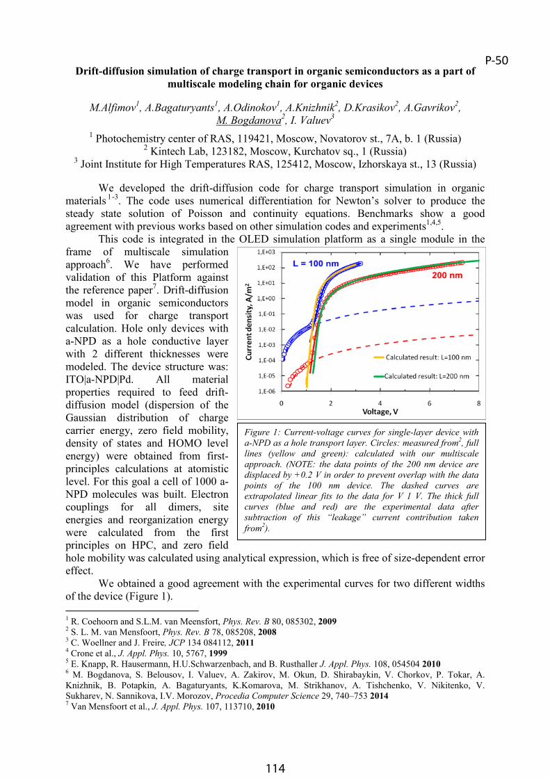
114
Drift-diffusion simulation of charge transport in organic semiconductors as a part of multiscale modeling chain for organic devices
M.Alfimov1, A.Bagaturyants1, A.Odinokov1, A.Knizhnik2, D.Krasikov2, A.Gavrikov2,M. Bogdanova2, I. Valuev3
1 Photochemistry center of RAS, 119421, Moscow, Novatorov st., 7A, b. 1 (Russia)2 Kintech Lab, 123182, Moscow, Kurchatov sq., 1 (Russia)
3 Joint Institute for High Temperatures RAS, 125412, Moscow, Izhorskaya st., 13 (Russia)
We developed the drift-diffusion code for charge transport simulation in organic materials 1-3. The code uses numerical differentiation for Newton’s solver to produce the steady state solution of Poisson and continuity equations. Benchmarks show a good agreement with previous works based on other simulation codes and experiments1,4,5.
This code is integrated in the OLED simulation platform as a single module in the frame of multiscale simulation approach6. We have performed validation of this Platform against the reference paper7. Drift-diffusion model in organic semiconductors was used for charge transport calculation. Hole only devices with a-NPD as a hole conductive layer with 2 different thicknesses were modeled. The device structure was: ITO|a-NPD|Pd. All material properties required to feed drift-diffusion model (dispersion of the Gaussian distribution of charge carrier energy, zero field mobility, density of states and HOMO level energy) were obtained from first-principles calculations at atomistic level. For this goal a cell of 1000 a-NPD molecules was built. Electron couplings for all dimers, site energies and reorganization energy were calculated from the first principles on HPC, and zero field hole mobility was calculated using analytical expression, which is free of size-dependent error effect.
We obtained a good agreement with the experimental curves for two different widths of the device (Figure 1).
1 R. Coehoorn and S.L.M. van Meensfort, Phys. Rev. B 80, 085302, 20092 S. L. M. van Mensfoort, Phys. Rev. B 78, 085208, 20083 C. Woellner and J. Freire, JCP 134 084112, 20114 Crone et al., J. Appl. Phys. 10, 5767, 19995 E. Knapp, R. Hausermann, H.U.Schwarzenbach, and B. Rusthaller J. Appl. Phys. 108, 054504 20106 M. Bogdanova, S. Belousov, I. Valuev, A. Zakirov, M. Okun, D. Shirabaykin, V. Chorkov, P. Tokar, A. Knizhnik, B. Potapkin, A. Bagaturyants, K.Komarova, M. Strikhanov, A. Tishchenko, V. Nikitenko, V. Sukharev, N. Sannikova, I.V. Morozov, Procedia Computer Science 29, 740–753 20147 Van Mensfoort et al., J. Appl. Phys. 107, 113710, 2010
Figure 1: Current-voltage curves for single-layer device with a-NPD as a hole transport layer. Circles: measured from2, full lines (yellow and green): calculated with our multiscale approach. (NOTE: the data points of the 200 nm device are displaced by +0.2 V in order to prevent overlap with the data points of the 100 nm device. The dashed curves are extrapolated linear fits to the data for V 1 V. The thick full curves (blue and red) are the experimental data after subtraction of this “leakage” current contribution taken from2).
P-50

115
Drift-diffusion simulation of charge transport in organic semiconductors as a part of multiscale modeling chain for organic devices
M.Alfimov1, A.Bagaturyants1, A.Odinokov1, A.Knizhnik2, D.Krasikov2, A.Gavrikov2,M. Bogdanova2, I. Valuev3
1 Photochemistry center of RAS, 119421, Moscow, Novatorov st., 7A, b. 1 (Russia)2 Kintech Lab, 123182, Moscow, Kurchatov sq., 1 (Russia)
3 Joint Institute for High Temperatures RAS, 125412, Moscow, Izhorskaya st., 13 (Russia)
We developed the drift-diffusion code for charge transport simulation in organic materials 1-3. The code uses numerical differentiation for Newton’s solver to produce the steady state solution of Poisson and continuity equations. Benchmarks show a good agreement with previous works based on other simulation codes and experiments1,4,5.
This code is integrated in the OLED simulation platform as a single module in the frame of multiscale simulation approach6. We have performed validation of this Platform against the reference paper7. Drift-diffusion model in organic semiconductors was used for charge transport calculation. Hole only devices with a-NPD as a hole conductive layer with 2 different thicknesses were modeled. The device structure was: ITO|a-NPD|Pd. All material properties required to feed drift-diffusion model (dispersion of the Gaussian distribution of charge carrier energy, zero field mobility, density of states and HOMO level energy) were obtained from first-principles calculations at atomistic level. For this goal a cell of 1000 a-NPD molecules was built. Electron couplings for all dimers, site energies and reorganization energy were calculated from the first principles on HPC, and zero field hole mobility was calculated using analytical expression, which is free of size-dependent error effect.
We obtained a good agreement with the experimental curves for two different widths of the device (Figure 1).
1 R. Coehoorn and S.L.M. van Meensfort, Phys. Rev. B 80, 085302, 20092 S. L. M. van Mensfoort, Phys. Rev. B 78, 085208, 20083 C. Woellner and J. Freire, JCP 134 084112, 20114 Crone et al., J. Appl. Phys. 10, 5767, 19995 E. Knapp, R. Hausermann, H.U.Schwarzenbach, and B. Rusthaller J. Appl. Phys. 108, 054504 20106 M. Bogdanova, S. Belousov, I. Valuev, A. Zakirov, M. Okun, D. Shirabaykin, V. Chorkov, P. Tokar, A. Knizhnik, B. Potapkin, A. Bagaturyants, K.Komarova, M. Strikhanov, A. Tishchenko, V. Nikitenko, V. Sukharev, N. Sannikova, I.V. Morozov, Procedia Computer Science 29, 740–753 20147 Van Mensfoort et al., J. Appl. Phys. 107, 113710, 2010
Figure 1: Current-voltage curves for single-layer device with a-NPD as a hole transport layer. Circles: measured from2, full lines (yellow and green): calculated with our multiscale approach. (NOTE: the data points of the 200 nm device are displaced by +0.2 V in order to prevent overlap with the data points of the 100 nm device. The dashed curves are extrapolated linear fits to the data for V 1 V. The thick full curves (blue and red) are the experimental data after subtraction of this “leakage” current contribution taken from2).
Differences in photochemical properties of phospholes and 1,2-diphospholes
T.I. Burganov*, S.A. Katsyuba, E.E. Zvereva, A.A. Zagidullin, V.A. Milyukov, O.G.Sinyashin.A.E. Arbuzov Institute of Organic and Physical Chemistry of Kazan Scientific Center of the
Russian Academy of Sciences*e-mail: [email protected] , [email protected]
The π-conjugated materials based on organophosphorus compounds represent a valuable addition to the pool of building blocks for molecular electronics. Phospholes (five-membered 6π-systems with one phosphorus atoms) as subunits for the π-conjugated systems are the most widely investigated P-heterocycles, because they display interesting electronic properties with both high electron-accepting and electron-transporting abilities. Abilities of 3,4,5-triaryl-1-R-1,2-diphospholes (DPs) to conjugation with exocyclic moieties are shown[1] to be very close to those of phospholes, but their luminescent properties are unknown. We have undertaken the first study of the emission spectra of DPs. According to the data obtained, these compounds in n-hexane solutions demonstrate moderate luminescence practically in the same range ~ 400-500 nm as related phospholes. At the same time, Stokes shift for DPs amounts to ~ 70 nm, which is considerably smaller than in the case of phospholes (~ 110 nm). It is shown that emission properties of DPs can be tuned by means of chemical modification of exocyclic aromatic moieties, but “structure-property” relations for emission spectra are dramatically different from those found earlier1 for absorption spectra.Problems with quantum-chemical description of these specific properties are discussed.
This work was supported by the Council on Grants of the Russian Federation President (MK- 7748.2015.3) and the Russian Foundation for Basic Research (№ 14-03-00920 А)
1 S. A. Katsyuba, T. I. Burganov, E. E. Zvereva, A. A. Zagidullin, V. A. Miluykov, P. Lönnecke, E. Hey-Hawkins, O. G. Sinyashin, J. Phys. Chem. A, 2014, 118, 12168-12177.
P-51

116
Conjugated Polyelectrolytes for Electronic and Optoelectronic Applications
S.E. Domínguez, P. Damlin, C. KvarnströmLaboratory of Materials Chemistry and Chemical Analysis, University of Turku, Finland
e-mail: [email protected]
Conjugated polyelectrolytes (CPEs) have a conjugated backbone (with pi-orbitals, which generate electron delocalization) and also polar functional groups (which generate solubility in polar solvents), reason why these molecules find applications both in solution and in solid state. In solution, their chromophore-fluorophore nature, together with all the driving forces of interaction CPEs have (pi-pi stacking, hydrophobic interactions, electrostatic forces and hydrogen bonding) make these molecules to aggregate in different modes, in function of their molecular structure and the surrounding media, reason why their optical properties have been exploited for sensing in solution.
In solid state, their polymeric and pi-conjugated nature makes them semiconductingand bendable, but also and thanks to their polar nature, important surface electronic properties emerge, such as permanent dipoles, which modifies the Fermi level, allowing fine-tune the work function and energy barriers. Also, their counter-ions allow on one hand, to tune theirinterfacial and charge-mobility properties, and on the other hand the possibility of mixed ionic-electronic transport. The solution-processability of CPEs allows roll-to-roll printing, or, when casted onto oppositely charged surfaces, layer-by-layer self-assembly through electrostatic interactions. On the other hand, when casted onto surfaces with orthogonal solubility, it is possible to obtain extremely defined interfaces. Because of these properties,CPEs have been applied in polymeric organic solar cells as active or electrode buffer layers,in hybrid solar cells, and also as interfacial layers in organic light emitting diodes and organic field-effect transistors.
This contribution will present an overview of our ongoing research on the solution and solid-state properties of a set of CPEs in different media, using different techniques, such as spectroscopic (absorption, fluorescence, FT-IR, electron paramagnetic resonance, photon correlation, intensity modulated photocurrent, impedance), molecular modeling (Density Functional Theory in solution), solid-state electrochemistry (galvanostatic and potentiostatic), spectro-electrochemistry, and also surface (contact angle goniometry, AFM) and structural (grazing incidence small angle x-ray scattering) analyses.
____________________________1 Bazan, G. C. and Liu, B. (ed). (2013). Conjugated Polyelectrolytes, Fundamentals and Applications. Weinheim, Germany: Wiley-VCH. 2 Leger, J., Berggren, M. and Carter, S. (2011). Iontronics, Ionic Carriers in Organic Electronic Materials and Devices. Boca Raton, FL: CRC Press.3 Lee, W., Seo, J. H. and Woo, H. Y. (2013). “Conjugated polyelectrolytes: A new class of semiconducting materials for organic electronic devices,” Polymer 54, 5104-5121.
P-52
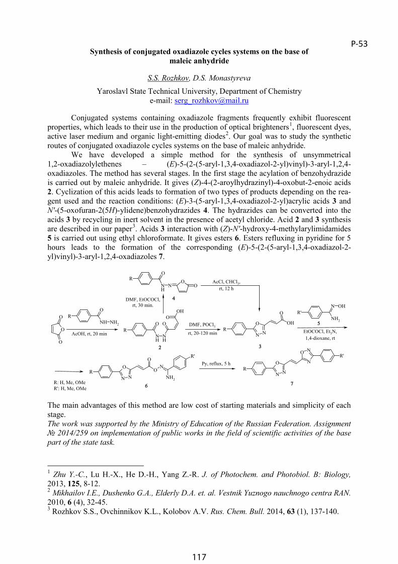
117
Synthesis of conjugated oxadiazole cycles systems on the base ofmaleic anhydride
S.S. Rozhkov, D.S. MonastyrevaYaroslavl State Technical University, Department of Chemistry
e-mail: [email protected]
Conjugated systems containing oxadiazole fragments frequently exhibit fluorescent properties, which leads to their use in the production of optical brighteners1, fluorescent dyes, active laser medium and organic light-emitting diodes2. Our goal was to study the synthetic routes of conjugated oxadiazole cycles systems on the base of maleic anhydride.
We have developed a simple method for the synthesis of unsymmetrical 1,2-oxadiazolylethenes – (E)-5-(2-(5-aryl-1,3,4-oxadiazol-2-yl)vinyl)-3-aryl-1,2,4-oxadiazoles. The method has several stages. In the first stage the acylation of benzohydrazide is carried out by maleic anhydride. It gives (Z)-4-(2-aroylhydrazinyl)-4-oxobut-2-enoic acids2. Cyclization of this acids leads to formation of two types of products depending on the rea-gent used and the reaction conditions: (E)-3-(5-aryl-1,3,4-oxadiazol-2-yl)acrylic acids 3 and N'-(5-oxofuran-2(5H)-ylidene)benzohydrazides 4. The hydrazides can be converted into the acids 3 by recycling in inert solvent in the presence of acetyl chloride. Acid 2 and 3 synthesisare described in our paper3. Acids 3 interaction with (Z)-N'-hydroxy-4-methylarylimidamides5 is carried out using ethyl chloroformate. It gives esters 6. Esters refluxing in pyridine for 5 hours leads to the formation of the corresponding (E)-5-(2-(5-aryl-1,3,4-oxadiazol-2-yl)vinyl)-3-aryl-1,2,4-oxadiazoles 7.
NH
O
NH2
R
O
O
ONH
O
NH
O
OHO
RO
N N
OH
O
R
NH2
N OHR'
O
N NO
ON
NH2
R'
R N N
O N
NOR'
R
NH
O
NO
OR
AcOH, rt, 20 min rt, 20-120 min
DMF, POCl3
2 3
5
6
EtOCOCl, Et3N, 1,4-dioxane, rt
Py, reflux, 5 h
R: H, Me, OMe 7
DMF, EtOCOCl,rt, 30 min.
AcCl, CHCl3,rt, 12 h
4
R': H, Me, OMe
The main advantages of this method are low cost of starting materials and simplicity of each stage.The work was supported by the Ministry of Education of the Russian Federation. Assignment № 2014/259 on implementation of public works in the field of scientific activities of the base part of the state task.
1 Zhu Y.-C., Lu H.-X., He D.-H., Yang Z.-R. J. of Photochem. and Photobiol. B: Biology,2013, 125, 8-12.2 Mikhailov I.E., Dushenko G.A., Elderly D.A. et. al. Vestnik Yuznogo nauchnogo centra RAN.2010, 6 (4), 32-45.3 Rozhkov S.S., Ovchinnikov K.L., Kolobov A.V. Rus. Chem. Bull. 2014, 63 (1), 137-140.
P-53

118
Increase of luminescence via small molecules alignment
A.V. Stankevich*, V.S. Bezruchenko, A.A. Muravsky, A.A. Murauski, V.E. Agabekov.Institute of Chemistry of New Materials NAS of Belarus
*e-mail: [email protected]
Organic semiconducting materials find its application for organic light emitting diodes(OLED)1 and organic field effect transistors. Electrical properties of these materials strongly depend on ordering of organic molecules inside thin film2. Molecular ordering dramatically changes the ionization potential3, light absorption and luminescence, carrier mobility, stability of the films4. Previously we found dependence of anchoring energy of PEDOT:PSS on order parameter of luminescence molecules5. In this work we investigate luminescence changes of model molecules of oligo(phenylenevinylene) dye wet coated on PEDOT:PSS alignment layer .
Films were prepared as following5: First, the solution of PEDOT:PSS BAYTRON® was rod-coated on glass substrate. The obtained PEDOT:PSS film was hotplate baked at 180 °C for 30 min and then rubbed.
We prepared rubbed and non-rubbed PEDOT:PSS films to study the difference in luminiscence. The films were rod-coated with oligo(phenylenevinylene) dye using 2% solution in chlorobenzene.
Oligo(phenylenevinylene) dyes form uniaxial films on rubbed PEDOT:PSS surface(fig. 1 a). Rubbed and non-rubbed surfaces give order parameters of the dye film 0.65 and 0.34, correspondingly. Ordered film luminesce is 20 times greater (fig. 1 a,b), which can be explained assuming that molucules on the non-rubbed surface have partialy vertical aligmentand light excitation in normal to the film surface. Also alignment could improve external quantum efficiency (EQE) of luminescence. Rubbed PEDOT:PSS films have high azimuthal anchoring energy and align molecules parallel to the surface. This method can increaseluminance of linear organic emitters both in wet and vacuum deposition process.
a bFigure 1 Anisotropic luminesence of oligo(phenylenevinylene) on (a) rubbed (b) non-rubbed
PEDOT:PSS surface
1 Hoi Nok Tsao, Don Cho, Jens Wenzel Andreasen et al., Advanced Materials 21 (2), 209 (2009).2 Martin Grell and Donal DC Bradley, Advanced Materials 11 (11), 895 (1999).3 Wei Chen, Han Huang, Shi Chen et al., Chemistry of Materials 20 (22), 7017 (2008).4 Laure Biniek, Stéphanie Pouget, David Djurado et al., Macromolecules (2014).5 A. Stankevich, V. Bezruchenko A. Muravsky et al., 46-3 SID Symposium Digest of Technical Papers 46 (2015).
P-54

Author index
Increase of luminescence via small molecules alignment
A.V. Stankevich*, V.S. Bezruchenko, A.A. Muravsky, A.A. Murauski, V.E. Agabekov.Institute of Chemistry of New Materials NAS of Belarus
*e-mail: [email protected]
Organic semiconducting materials find its application for organic light emitting diodes(OLED)1 and organic field effect transistors. Electrical properties of these materials strongly depend on ordering of organic molecules inside thin film2. Molecular ordering dramatically changes the ionization potential3, light absorption and luminescence, carrier mobility, stability of the films4. Previously we found dependence of anchoring energy of PEDOT:PSS on order parameter of luminescence molecules5. In this work we investigate luminescence changes of model molecules of oligo(phenylenevinylene) dye wet coated on PEDOT:PSS alignment layer .
Films were prepared as following5: First, the solution of PEDOT:PSS BAYTRON® was rod-coated on glass substrate. The obtained PEDOT:PSS film was hotplate baked at 180 °C for 30 min and then rubbed.
We prepared rubbed and non-rubbed PEDOT:PSS films to study the difference in luminiscence. The films were rod-coated with oligo(phenylenevinylene) dye using 2% solution in chlorobenzene.
Oligo(phenylenevinylene) dyes form uniaxial films on rubbed PEDOT:PSS surface(fig. 1 a). Rubbed and non-rubbed surfaces give order parameters of the dye film 0.65 and 0.34, correspondingly. Ordered film luminesce is 20 times greater (fig. 1 a,b), which can be explained assuming that molucules on the non-rubbed surface have partialy vertical aligmentand light excitation in normal to the film surface. Also alignment could improve external quantum efficiency (EQE) of luminescence. Rubbed PEDOT:PSS films have high azimuthal anchoring energy and align molecules parallel to the surface. This method can increaseluminance of linear organic emitters both in wet and vacuum deposition process.
a bFigure 1 Anisotropic luminesence of oligo(phenylenevinylene) on (a) rubbed (b) non-rubbed
PEDOT:PSS surface
1 Hoi Nok Tsao, Don Cho, Jens Wenzel Andreasen et al., Advanced Materials 21 (2), 209 (2009).2 Martin Grell and Donal DC Bradley, Advanced Materials 11 (11), 895 (1999).3 Wei Chen, Han Huang, Shi Chen et al., Chemistry of Materials 20 (22), 7017 (2008).4 Laure Biniek, Stéphanie Pouget, David Djurado et al., Macromolecules (2014).5 A. Stankevich, V. Bezruchenko A. Muravsky et al., 46-3 SID Symposium Digest of Technical Papers 46 (2015).

120
AH. AbdallaV.E. AgabekovE.V. AginaA.V. AkkuratovS. AlamO.A. AlekseevaM. AlfimovT. AmeriB.A. AndreevD. AndrienkoD.S. AnisimovS. Athanasopoulos
BA. BagaturyantsF.J. BahnamiriA.V. BakirovH.J. BakkerA.A. BakulinS.V. BalakhonovM.Yu. BalakinaD.S. BaranovH. BässlerS.L. BaylissCh.S. BeckerN.A. BelichI.A. BelogorokhovS. BelousovP.R. BergerA.A. BessonovV.S. BezruchenkoF. BiscariniI.I. BobrinetskiyM.N. BochkarevM. BogdanovaO. BogomolovaA. BonfiglioO.V. Borshchev
H. BouchiatC.J. BrabecJ.-L. BrédasV.V. BruevichT.I. BurganovI. Burgués-CeballosM.E. BurinM.I. Buzin
4811841, 42, 43, 66, 103108658811497, 109903541, 42, 66, 6749
114559730, 6730, 677584, 9310549506875, 80701132443, 691182372, 7389, 90113, 1143161, 6340, 41, 42, 43, 58, 59, 60, 66, 79, 96, 98, 100, 103, 1075013, 54, 97, 10930, 3540, 59, 60, 66, 67, 741151029079
CD. CahenA.D. ChepelianskiiE. ChoS.A. ChoulisS.N. ChvalunS. ContiV. CoropceanuP. CossedduA. Crha
DP. DamlinM. DefourD. de LeeuwA. Di CarloP.V. DmitryakovS.E. DomínguezD.I. DominskyM.A. DronovF.V. DrozdovT.V. DubininaV. Dyakonov
EA.V. EmelianovV.V. ErokhinF. Etzold
FT. FaberA.F. FacchettiY.V. FedorovI.V. FedorovE.V. FeldmanN. FelekidisI.I. FishchukO.D. FominykhA. FonariR.H. FriendL.A. Frolova
GA.Yu. GavrikA. GavrikovN.C. GeenhamR.Y.N. GenglerM. GibertiniJ. Gierschner
30503510241, 54, 97613061, 6399
11652, 53141654, 97, 1091166962, 7054, 71, 1096219, 71
72, 738517
11127, 5758, 987360, 69, 74514984, 93305029
71, 7411450423915, 94

121
E.M. GlebovD.Yu. GodovskyE.A. GoodilinV.V. GrebenevA.V. GrigorievaC. GuiducciM.G. GuschinA.-A.D. Guseynov
HS.T. HoffmannH. HoppeJ.C. Hummelen
IA. ImramovskýL.N. InasaridzeO. InganäsD. IvanovV. IvanovO.P. Ivanova
KA. KadashchukF.-J. KahleA.A. KalininS.A. KatsyubaM.S. KazantsevM. KemerinkS. KilchenmannS. KirchmeyerM. KirikovaE.A. KleymyukI.V. KlimovichA. KnizhnikV.M. KobryanskiiA. KöhlerE.A. KolesnikovA.S. KomolovM. KondratenkoA.N. KorovinL.J.A. KosterM.S. KotovaJ. KoutnýO.V. KozlovJ. KrajčovičD. KrasikovK. KremerE.P. Krinichnaya
10531, 4475, 76, 808875, 76, 80917276
4965, 11155
8129, 5617213577
49788411559, 68, 10517, 48, 5191254379561142049, 788033318547, 5562, 708145, 74951143577
Y. KrupskayaA.V. KubarkovL.G. KudryashovaL.V. KulikI.E. KuznetsovC. Kvarnström
LS. LaiF. LaquaiA.S. LeonovaA.I. LevitskayaI.G. LezamaM. LinaresR. LovrincicS. LuňákYu.N. Luponosov
M.S. Lyasnikova
MDonnge MaI.V. MartynovA. MalafeevN. MarzariA.A. MannanovA.L. MannanovT.J. MarksY.N. MalakhovaYu.S. MarfinA.A. MaleevA. MelianasF.S. MelkonyanK.A. MilakinB. Milián-MedinaV.A. MilyukovJ. MinD.S. MonastyrevaA.F. MorpurgoE.A. MostovichO.A. MukhachevaA.A. MurauskiA.A. MuravskyA.M. Muzafarov
NA.G. NasibulinA. NaumovP.K. Nayak
39, 8283, 10440, 59, 10787, 105108116
61, 631783848246308140, 54, 60, 71, 86, 97, 102, 109, 11088
2629353942, 7486, 102578589891757839411554, 97, 10911739, 8268, 1055611811879
3210630
122
V.R. NikitenkoS.V. Novikov
OM.A. ObrezkovaA. Odinokov
PG.L. PakhomovD.Yu. Paraschuk
S.K. ParkS.Y. ParkK. PaukS.M. PeregudovaC. PoelkingI. PolishchukS.A. Ponomarenko
A.G. PopovV.A. PostnikovF.A. PrudnovM.S. PshenichnikovA.P. PushkarevO.A. Pyshkina
RM.A. RatnerY.L.A. RezusC. RiskoR. RoeschA.V. RogachevE. RolloA.V. RomashkinJ. RoncaliS.S. RozhkovR. RuzickaT.V. Rybalova
SE.L. Sanchez-VeraN.A. SannikovaA.Y. SauninaT.J. SavenijeA. Savva
9236
109114
10137, 40, 42, 44, 45, 59, 60, 66, 67, 69, 74, 86, 102, 10794948154, 1093511340, 41, 42, 43, 54, 58, 59, 60, 66, 67, 71, 79, 86, 96, 97, 98, 100, 102, 103, 107, 109, 11087, 10540, 59, 8810840, 42, 4589, 9083, 104
11230, 6735111859172, 73181179959
91929217102
M.S. ScherbinaO. SeligV.G. SergeyevA.V. SharipovaT.S. SherkarJ. ShiV. SimekC.R. SinghO.G. SinyashinM. SionováA.S. SizovM.S. SkorotetckyA.N. SolodukhinN.I. SorokinaA.Yu. SosorevA. SpanuS. StafströmA.V. StankevichT.Yu. StarikovaS. StriteskyA.A. StupnikovP.A. StuzhinN.M. Surin
D.K. SusarovaE.A. Svidchenko
TV.A. TafeenkoA.S. TereshchenkoS. TorabiL. TorsiV.V. TravkinP.A. TroshinV.A. TrukhanovA.A. TrulK.A. TsarikS. TscheuschnerP.I. Turkina
UM.N. Uvarov
VM. ValaI. ValuevG. Van AsscheK. Van de RuitN. Van den Brande
9730, 6731, 83, 10493479499651159541, 43, 10358, 96, 10054, 86, 97, 102, 1108844634611898998510158, 79, 96, 98, 100, 10929, 56, 10858, 98
59100552210129, 5686, 1021037278104
87, 105
81, 95, 99113, 11452, 534852, 53

123
C. Van DyckB. Van MeleS. VargheseS.Z. VatsadzeM.V. VenerF. ViolaR. Volpi
WE. WangM. Weiter
XYu Xi
YA.N. YablonskiyS.-J. Yoon
ZA.A. ZagidullinS.A. ZavyalovA. ZhugayevychT.S. ZhuravlevaE.E. Zvereva
11252, 539475346346
5181, 95, 99
30
9094
1157710677115

IFSOE 2015www.ispm.ru/ifsoe-2015
Sponsors
DMITRY ZIMINFOUNDATIONDYNASTY
The school is supported by
The conference is supported by
RUSSIANFOUNDATIONFOR BASICREASERCH