2009 IMPACT Workshop - University of California, San...
52
IMPACT • CMP • 1 10/2/09 Faculty Presentation: CMP By David Dornfeld, Mechanical Engineering, UC-Berkeley 2009 IMPACT Workshop
Transcript of 2009 IMPACT Workshop - University of California, San...
IMPACT • CMP • 1 10/2/09
Faculty Presentation: CMPBy David Dornfeld, Mechanical Engineering, UC-Berkeley
2009 IMPACT Workshop
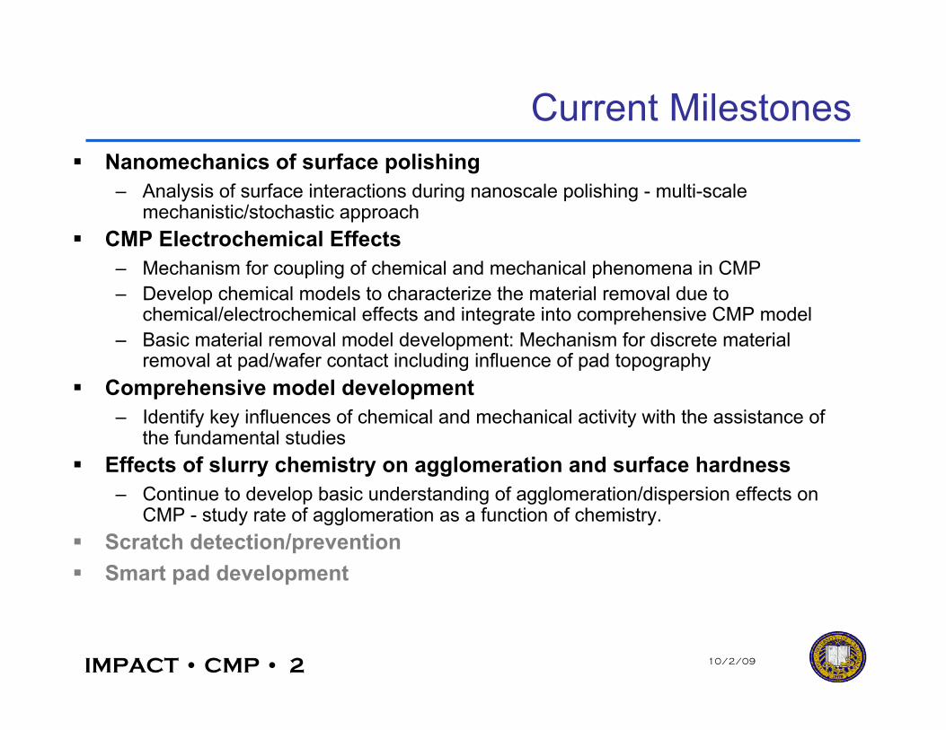
IMPACT • CMP • 2 10/2/09
Current Milestones Nanomechanics of surface polishing
– Analysis of surface interactions during nanoscale polishing - multi-scalemechanistic/stochastic approach
CMP Electrochemical Effects– Mechanism for coupling of chemical and mechanical phenomena in CMP– Develop chemical models to characterize the material removal due to
chemical/electrochemical effects and integrate into comprehensive CMP model– Basic material removal model development: Mechanism for discrete material
removal at pad/wafer contact including influence of pad topography Comprehensive model development
– Identify key influences of chemical and mechanical activity with the assistance ofthe fundamental studies
Effects of slurry chemistry on agglomeration and surface hardness– Continue to develop basic understanding of agglomeration/dispersion effects on
CMP - study rate of agglomeration as a function of chemistry. Scratch detection/prevention Smart pad development
10/2/09IMPACT • CMP • 3
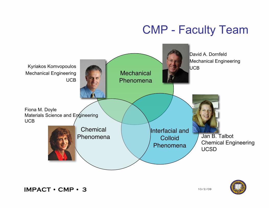
CMP - Faculty Team
MechanicalPhenomena
ChemicalPhenomena
Interfacial andColloid
PhenomenaJan B. TalbotChemical EngineeringUCSD
David A. DornfeldMechanical EngineeringUCB
Fiona M. DoyleMaterials Science and EngineeringUCB
Kyriakos KomvopoulosMechanical Engineering
UCB
10/2/09IMPACT • CMP • 4
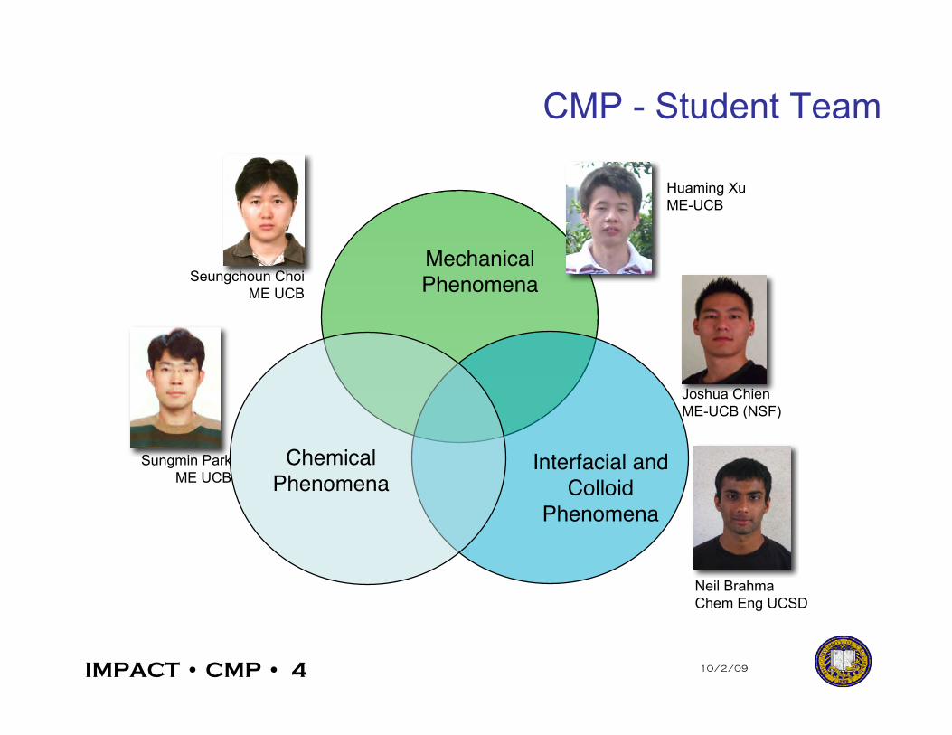
CMP - Student Team
MechanicalPhenomena
ChemicalPhenomena
Interfacial andColloid
Phenomena
Neil BrahmaChem Eng UCSD
Sungmin ParkME UCB
Huaming Xu ME-UCB
Joshua ChienME-UCB (NSF)
Seungchoun ChoiME UCB
IMPACT • CMP • 5 10/2/09
Head
Platen
Paddo
wn-
forc
e
slurrysupply
rotationof wafer
head
Wafer 4-12”
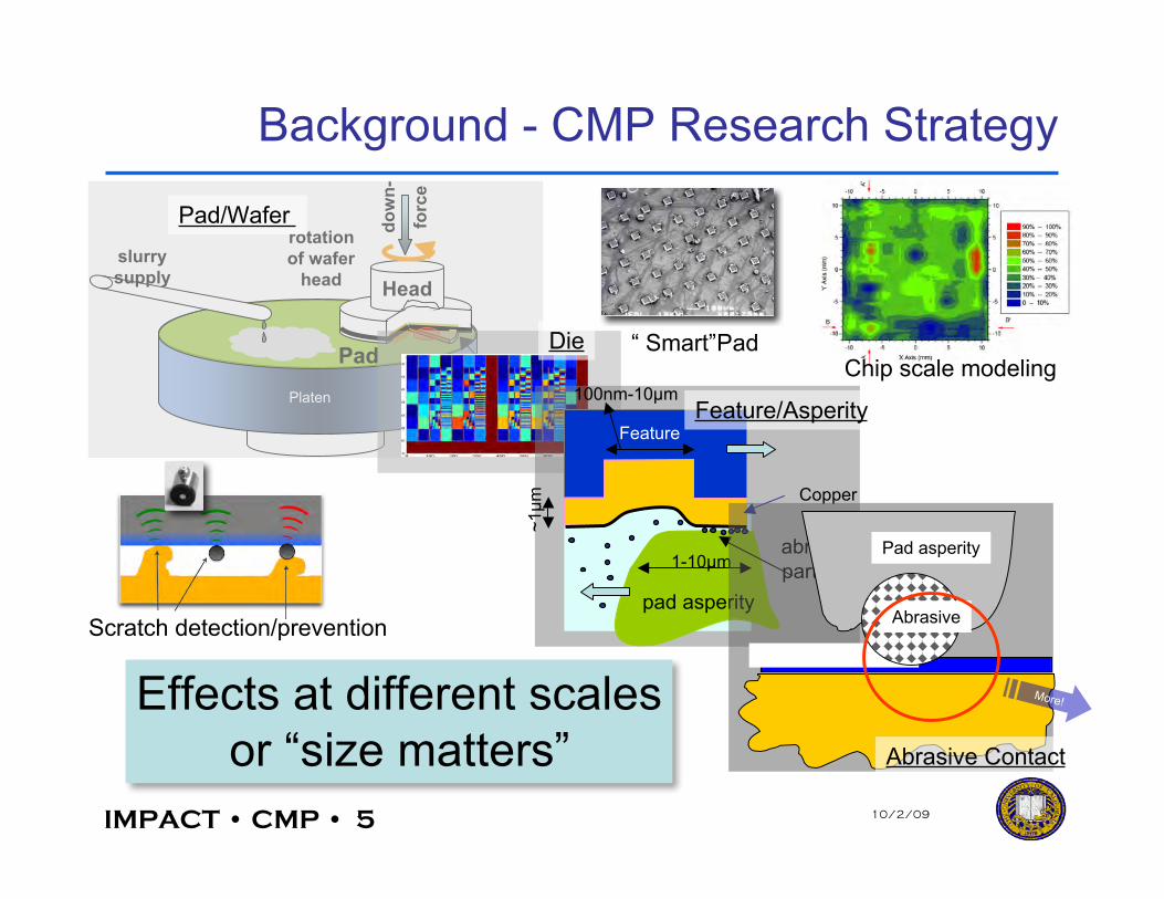
Background - CMP Research Strategy
Effects at different scalesor “size matters”
Copper
Feature
pad asperity
abrasiveparticles
100nm-10µm
~1µm
1-10µmPad asperity
Abrasive
Pad/Wafer
Die
Feature/Asperity
Abrasive Contact
More!
Chip scale modeling
Scratch detection/prevention
“ Smart”Pad
IMPACT • CMP • 6 10/2/09
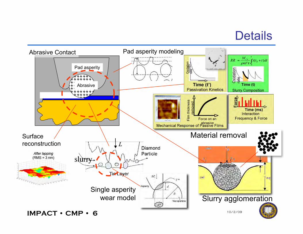
Pad asperity
Abrasive
Abrasive Contact
Details
Slurry agglomerationSingle asperity
wear model
Material removalSurface reconstruction
Pad asperity modeling
IMPACT • CMP • 7 10/2/09
Details on the posters!
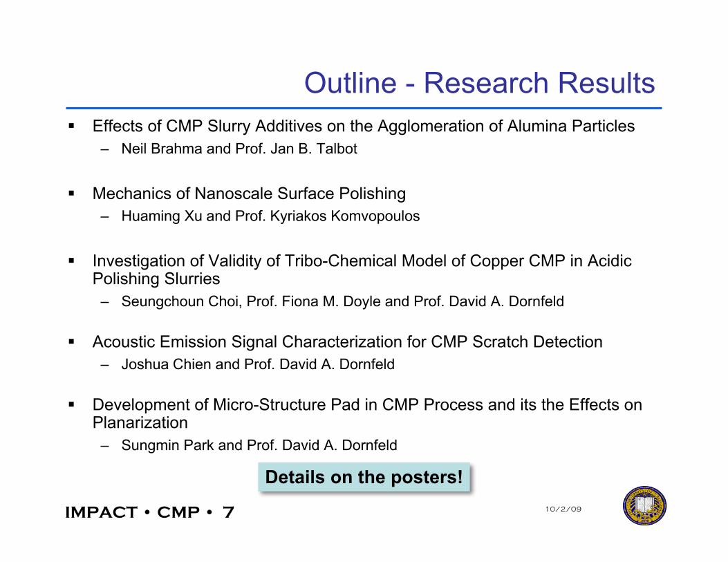
Outline - Research Results Effects of CMP Slurry Additives on the Agglomeration of Alumina Particles
– Neil Brahma and Prof. Jan B. Talbot
Mechanics of Nanoscale Surface Polishing– Huaming Xu and Prof. Kyriakos Komvopoulos
Investigation of Validity of Tribo-Chemical Model of Copper CMP in AcidicPolishing Slurries– Seungchoun Choi, Prof. Fiona M. Doyle and Prof. David A. Dornfeld
Acoustic Emission Signal Characterization for CMP Scratch Detection– Joshua Chien and Prof. David A. Dornfeld
Development of Micro-Structure Pad in CMP Process and its the Effects onPlanarization– Sungmin Park and Prof. David A. Dornfeld
IMPACT • CMP • 8 10/2/09
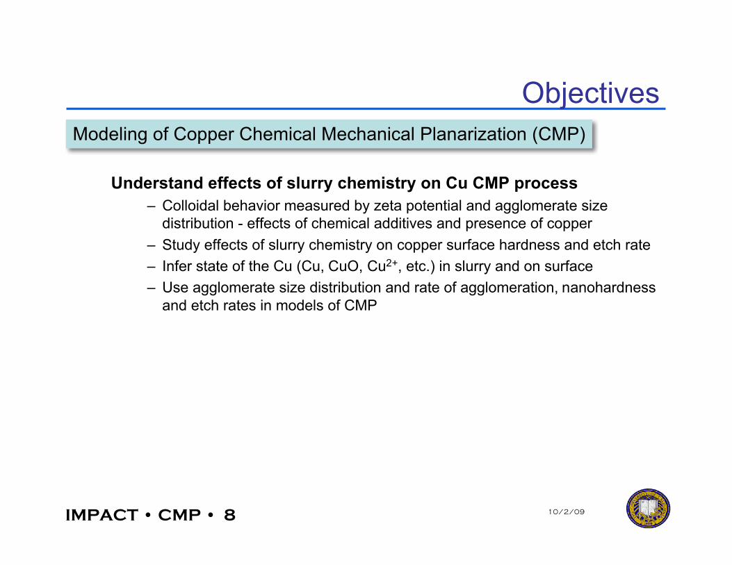
Objectives
Understand effects of slurry chemistry on Cu CMP process– Colloidal behavior measured by zeta potential and agglomerate size
distribution - effects of chemical additives and presence of copper– Study effects of slurry chemistry on copper surface hardness and etch rate– Infer state of the Cu (Cu, CuO, Cu2+, etc.) in slurry and on surface– Use agglomerate size distribution and rate of agglomeration, nanohardness
and etch rates in models of CMP
Modeling of Copper Chemical Mechanical Planarization (CMP)
IMPACT • CMP • 9 10/2/09IMPACT - Poster Presentation
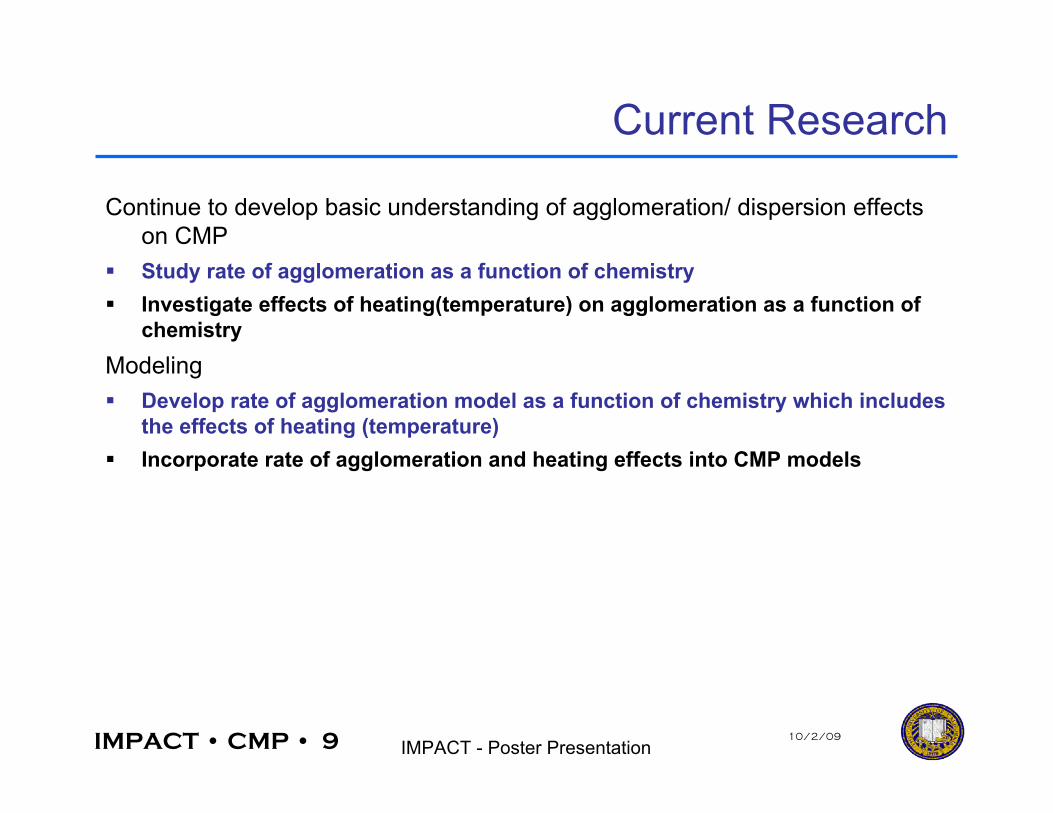
Current Research
Continue to develop basic understanding of agglomeration/ dispersion effectson CMP
Study rate of agglomeration as a function of chemistry Investigate effects of heating(temperature) on agglomeration as a function of
chemistryModeling Develop rate of agglomeration model as a function of chemistry which includes
the effects of heating (temperature) Incorporate rate of agglomeration and heating effects into CMP models
IMPACT • CMP • 10 10/2/09
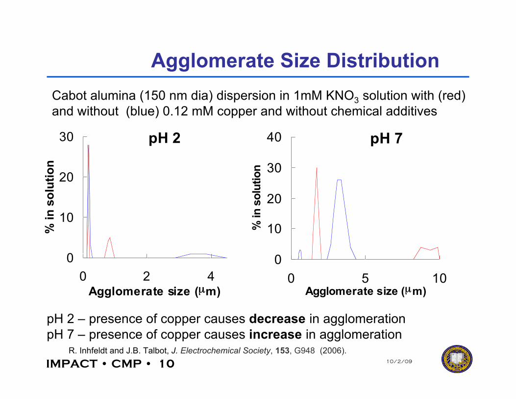
Agglomerate Size Distribution
pH 2 – presence of copper causes decrease in agglomerationpH 7 – presence of copper causes increase in agglomeration
Cabot alumina (150 nm dia) dispersion in 1mM KNO3 solution with (red)and without (blue) 0.12 mM copper and without chemical additives
pH 2
0
10
20
30
0 2 4
Agglomerate size (µm)
% in
so
luti
on
pH 7
0
10
20
30
40
0 5 10
Agglomerate size (µm)
% in
so
lutio
n
R. Inhfeldt and J.B. Talbot, J. Electrochemical Society, 153, G948 (2006).
IMPACT • CMP • 11 10/2/09
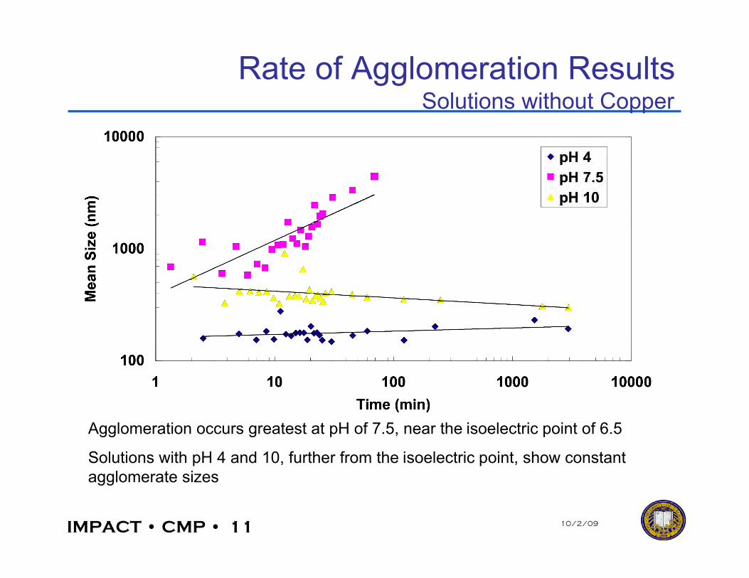
Rate of Agglomeration ResultsSolutions without Copper
Agglomeration occurs greatest at pH of 7.5, near the isoelectric point of 6.5
Solutions with pH 4 and 10, further from the isoelectric point, show constantagglomerate sizes
IMPACT • CMP • 12 10/2/09
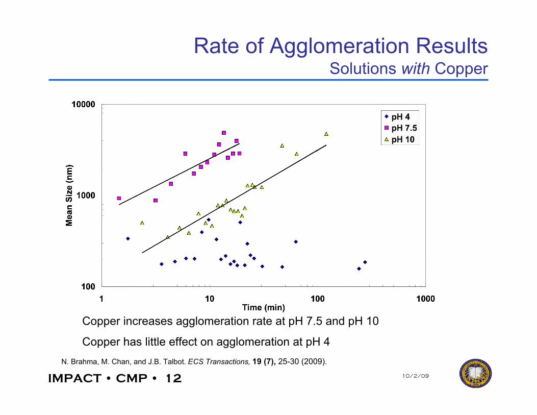
Rate of Agglomeration ResultsSolutions with Copper
Copper increases agglomeration rate at pH 7.5 and pH 10
Copper has little effect on agglomeration at pH 4N. Brahma, M. Chan, and J.B. Talbot. ECS Transactions, 19 (7), 25-30 (2009).
IMPACT • CMP • 13 10/2/09
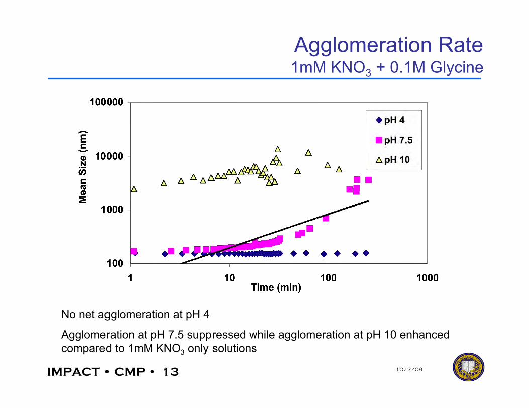
Agglomeration Rate1mM KNO3 + 0.1M Glycine
No net agglomeration at pH 4
Agglomeration at pH 7.5 suppressed while agglomeration at pH 10 enhancedcompared to 1mM KNO3 only solutions
IMPACT • CMP • 14 10/2/09
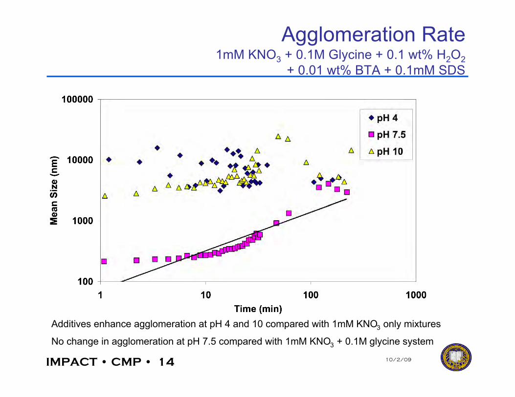
Agglomeration Rate1mM KNO3 + 0.1M Glycine + 0.1 wt% H2O2
+ 0.01 wt% BTA + 0.1mM SDS
Additives enhance agglomeration at pH 4 and 10 compared with 1mM KNO3 only mixtures
No change in agglomeration at pH 7.5 compared with 1mM KNO3 + 0.1M glycine system
IMPACT • CMP • 15 10/2/09
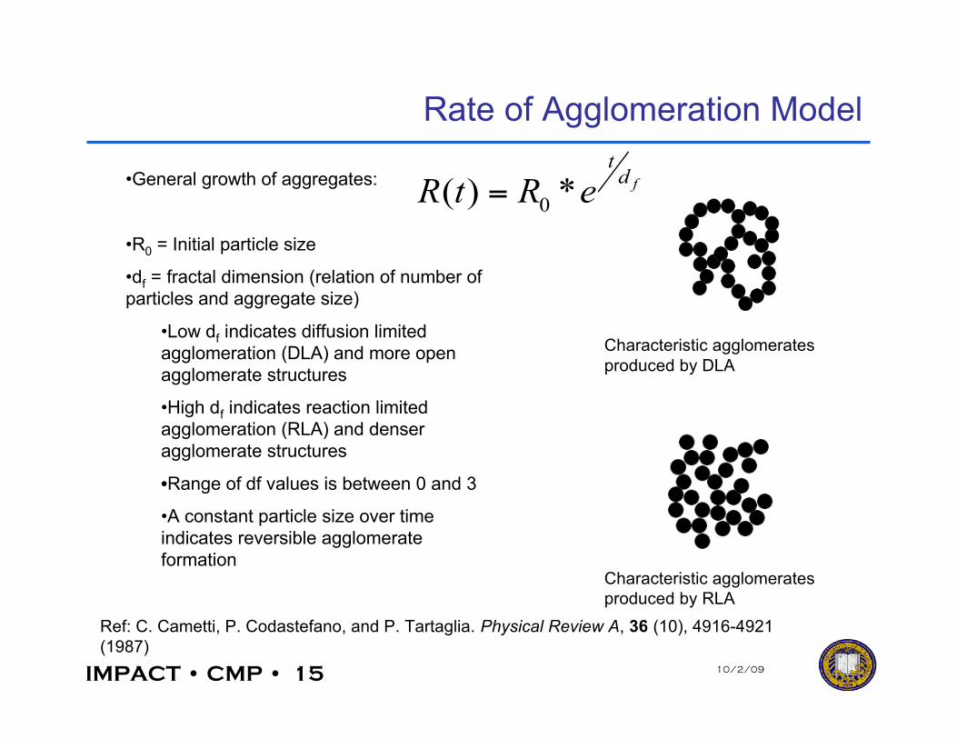
Rate of Agglomeration Model
•General growth of aggregates:
•R0 = Initial particle size
•df = fractal dimension (relation of number ofparticles and aggregate size)
•Low df indicates diffusion limitedagglomeration (DLA) and more openagglomerate structures
•High df indicates reaction limitedagglomeration (RLA) and denseragglomerate structures
•Range of df values is between 0 and 3
•A constant particle size over timeindicates reversible agglomerateformation
Ref: C. Cametti, P. Codastefano, and P. Tartaglia. Physical Review A, 36 (10), 4916-4921(1987)
Characteristic agglomeratesproduced by DLA
Characteristic agglomeratesproduced by RLA
0( ) * f
td
R t R e=
IMPACT • CMP • 16 10/2/09
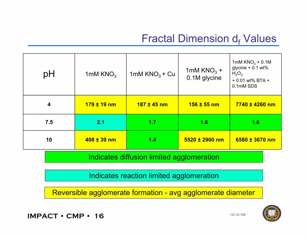
Fractal Dimension df Values
pH 1mM KNO3 1mM KNO3 + Cu 1mM KNO3 +0.1M glycine
1mM KNO3 + 0.1Mglycine + 0.1 wt%H2O2
+ 0.01 wt% BTA +0.1mM SDS
4 179 ± 19 nm 187 ± 45 nm 156 ± 55 nm 7740 ± 4260 nm
7.5 2.1 1.7 1.6 1.6
10 408 ± 39 nm 1.4 5520 ± 2900 nm 6580 ± 3670 nm
Reversible agglomerate formation - avg agglomerate diameter
Indicates reaction limited agglomeration
Indicates diffusion limited agglomeration
IMPACT • CMP • 17 10/2/09
Conclusions
• Effect of pH and Copper on Agglomeration Rate• Rates of agglomeration are sensitive to slurry pH• Copper has little effect on agglomeration at low pH, but causes slurries ata pH nearer the IEP or higher to agglomerate more quickly• Both presence of copper and pH affect agglomeration mechanism
• Effect of Additives on Agglomeration Rate• Glycine has no effect on pH 4, but suppresses agglomeration at pH 7.5and enhances it at pH 10• Addition of H2O2, BTA, and SDS have no effect on pH 7.5 compared toKNO3 + glycine, however enhanced aggregation at pH 4 and pH 10 isobserved
IMPACT • CMP • 18 10/2/09
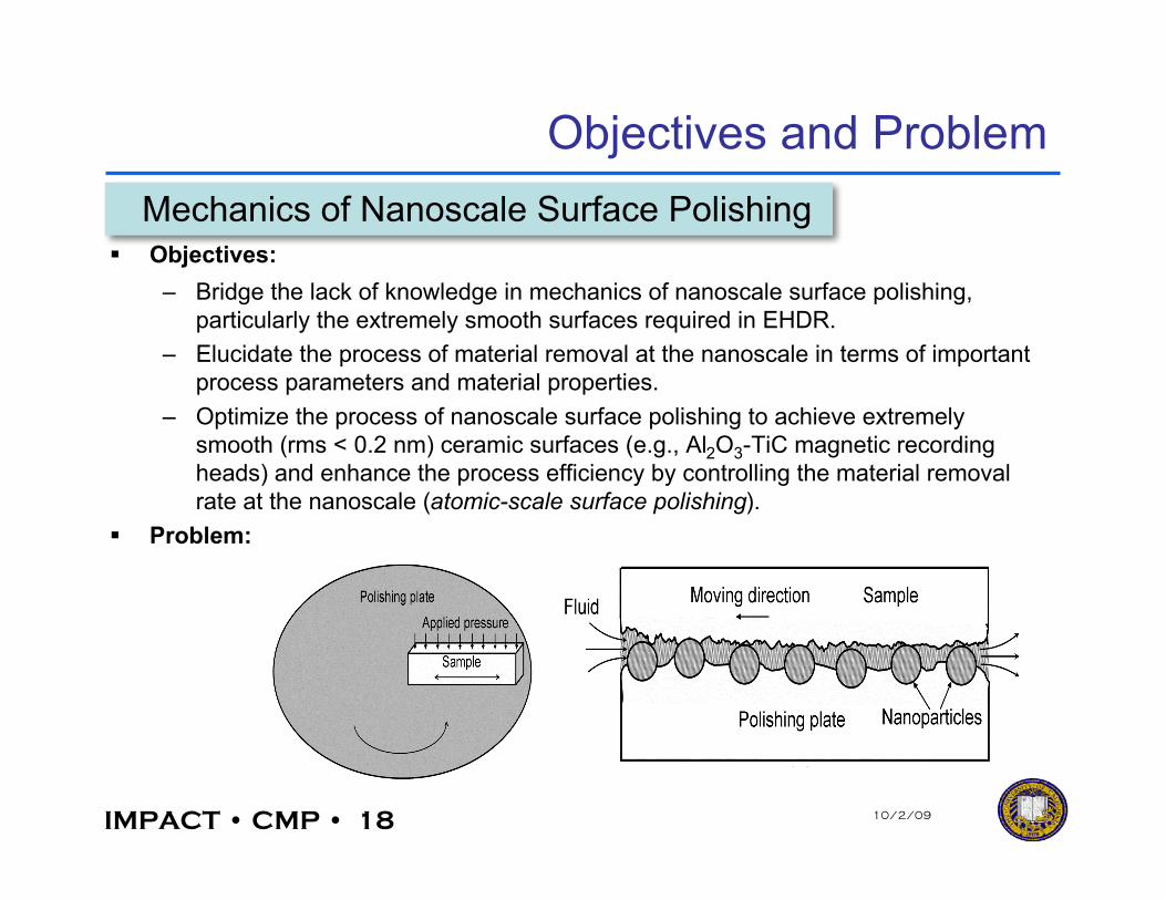
Objectives and Problem
Objectives:– Bridge the lack of knowledge in mechanics of nanoscale surface polishing,
particularly the extremely smooth surfaces required in EHDR.– Elucidate the process of material removal at the nanoscale in terms of important
process parameters and material properties.– Optimize the process of nanoscale surface polishing to achieve extremely
smooth (rms < 0.2 nm) ceramic surfaces (e.g., Al2O3-TiC magnetic recordingheads) and enhance the process efficiency by controlling the material removalrate at the nanoscale (atomic-scale surface polishing).
Problem:
Mechanics of Nanoscale Surface Polishing
IMPACT • CMP • 19 10/2/09
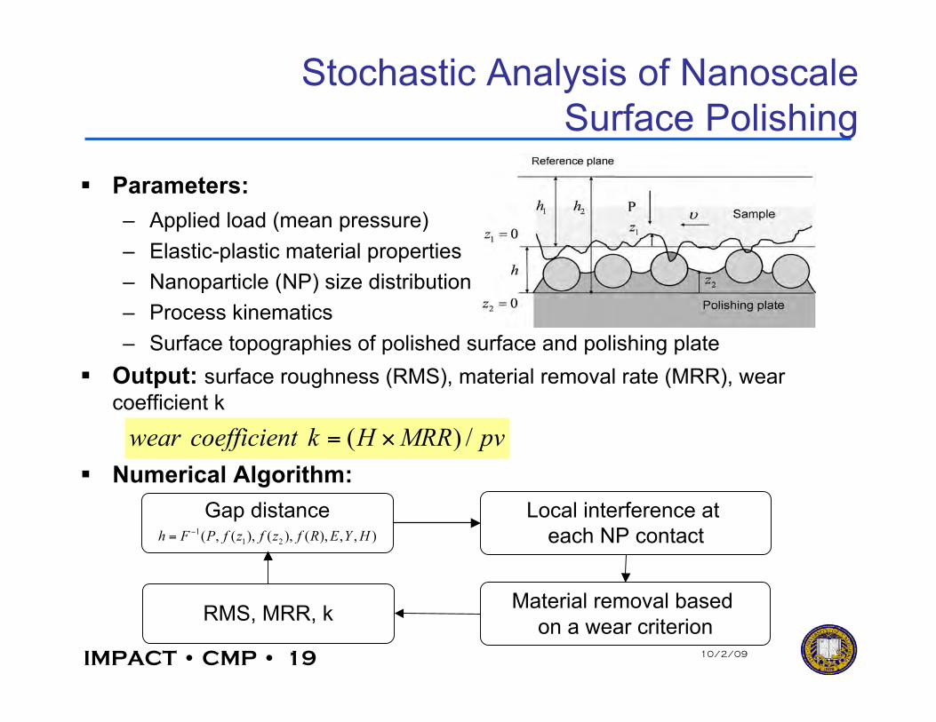
Stochastic Analysis of NanoscaleSurface Polishing
Parameters:– Applied load (mean pressure)– Elastic-plastic material properties– Nanoparticle (NP) size distribution– Process kinematics– Surface topographies of polished surface and polishing plate
Output: surface roughness (RMS), material removal rate (MRR), wearcoefficient k
Numerical Algorithm:( ) /wear coefficient k H MRR pv= !
RMS, MRR, k
Local interference at each NP contact
Gap distance1
1 2( , ( ), ( ), ( ), , , )h F P f z f z f R E Y H!=
Material removal based on a wear criterion
IMPACT • CMP • 20 10/2/09
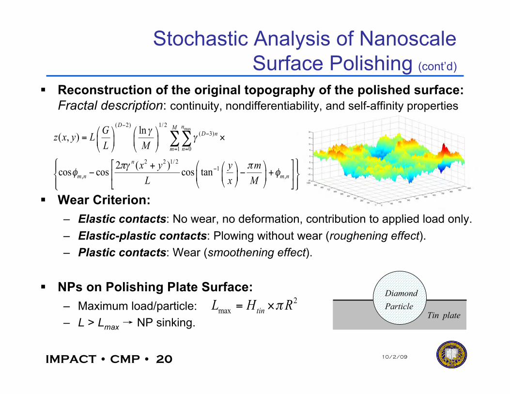
Stochastic Analysis of NanoscaleSurface Polishing (cont’d)
Reconstruction of the original topography of the polished surface:Fractal description: continuity, nondifferentiability, and self-affinity properties
Wear Criterion:– Elastic contacts: No wear, no deformation, contribution to applied load only.– Elastic-plastic contacts: Plowing without wear (roughening effect).– Plastic contacts: Wear (smoothening effect).
NPs on Polishing Plate Surface:– Maximum load/particle:– L > Lmax → NP sinking.
max( 2) 1/ 2
( 3)
1 0
2 2 1/ 21
, ,
ln( , )
2 ( )cos cos cos tan
D nMD n
m n
n
m n m n
Gz x y L
L M
x y y m
L x M
!!
"! "# #
$
$
= =
$
% & % &= '( ) ( )
* + * +
, -. /% &+0 0% &$ $ +1 23 4( )( )
* +* +0 05 67 8
99
Tin plate
Diamond
Particle2
max tinL H R!= "
IMPACT • CMP • 21 10/2/09
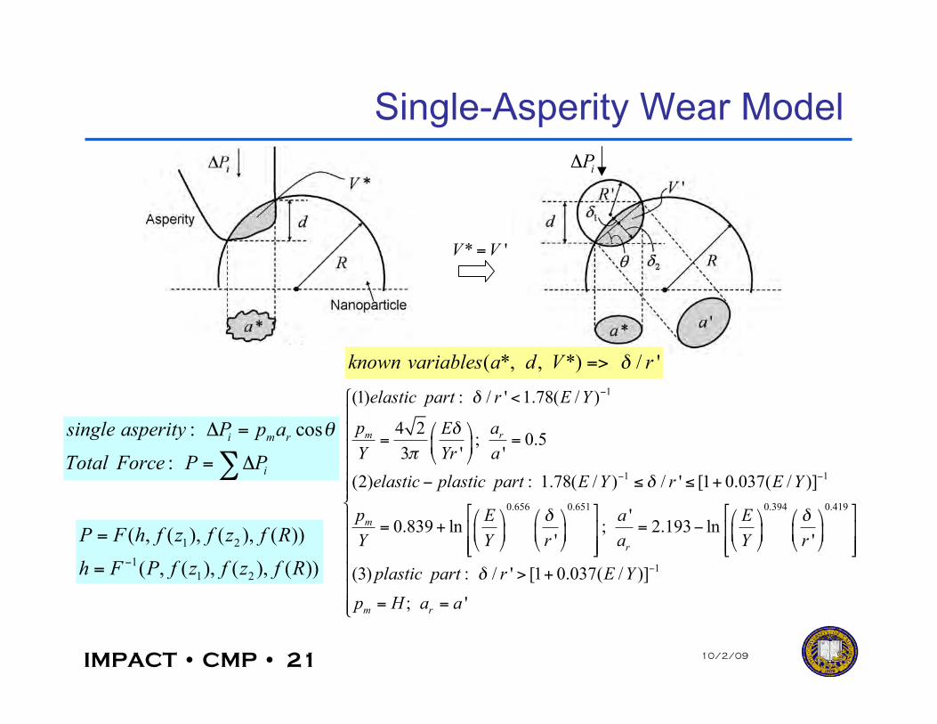
Single-Asperity Wear Model
1
1 1
0.656 0.651 0.394 0.
(1) : / ' 1.78( / )
4 2; 0.5
3 ' '
(2) : 1.78( / ) / ' [1 0.037( / )]
'0.839 ln ; 2.193 ln
' '
m r
m
r
elastic part r E Y
p aE
Y Yr a
elastic plastic part E Y r E Y
p E a E
Y Y r a Y r
!
!
"
!
! !
#
# #
<
$ %= =& '
( )
# * * +
+ ,$ % $ % $ % $ %= + = #- .& ' & ' & ' & '
( ) ( ) ( ) ( )- ./ 0
419
1(3) : / ' [1 0.037( / )]
; 'm r
plastic part r E Y
p H a a
! #
12222223
+ ,2- .2 - ./ 02
2 > +2
= =24
: cos
:
i m r
i
single asperity P p a
Total Force P P
!" =
= "#
1 2
1
1 2
( , ( ), ( ), ( ))
( , ( ), ( ), ( ))
P F h f z f z f R
h F P f z f z f R!
=
=
* 'V V=
iP!
( *, , *) / 'known variables a d V r!=>
IMPACT • CMP • 22 10/2/09
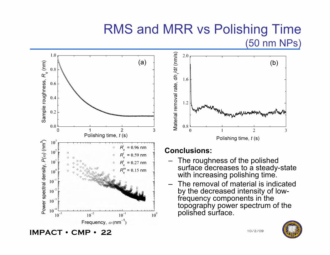
RMS and MRR vs Polishing Time(50 nm NPs)
Conclusions:– The roughness of the polished
surface decreases to a steady-statewith increasing polishing time.
– The removal of material is indicatedby the decreased intensity of low-frequency components in thetopography power spectrum of thepolished surface.
IMPACT • CMP • 23 10/2/09
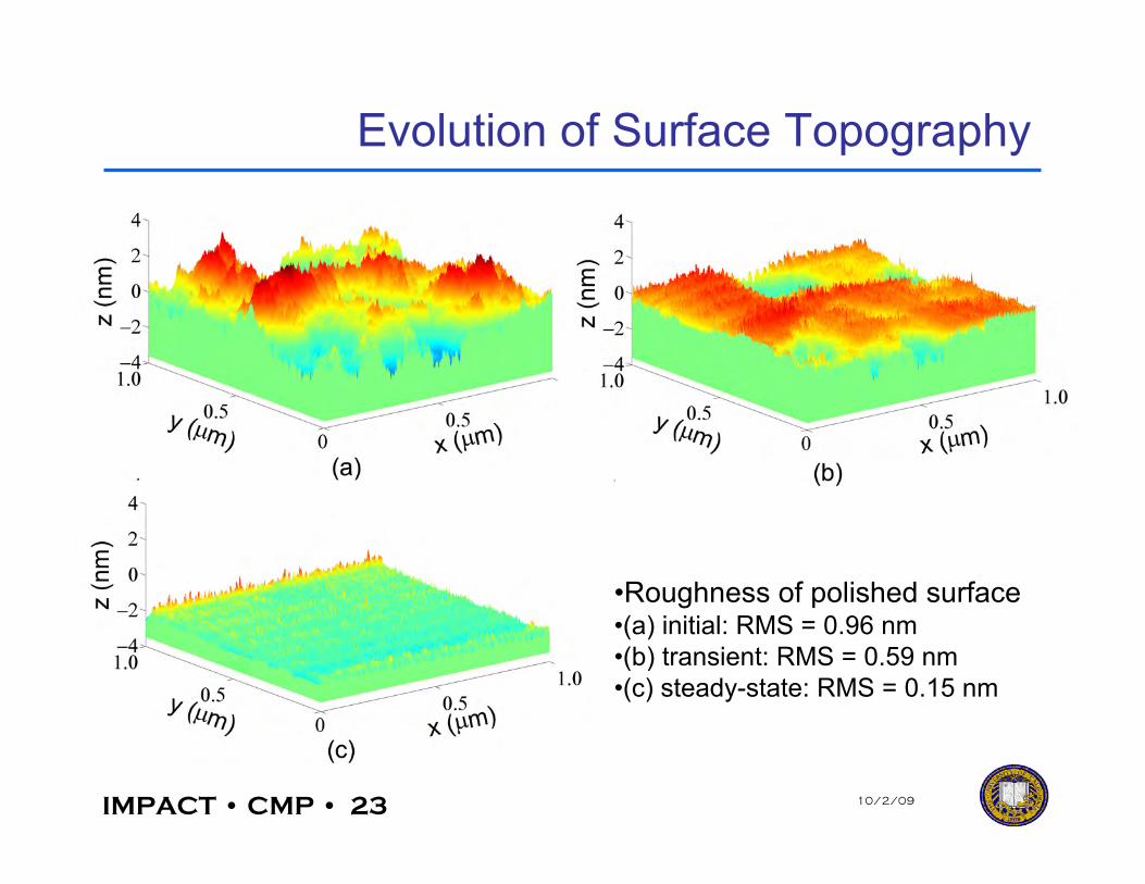
Evolution of Surface Topography
•Roughness of polished surface•(a) initial: RMS = 0.96 nm•(b) transient: RMS = 0.59 nm•(c) steady-state: RMS = 0.15 nm
IMPACT • CMP • 24 10/2/09
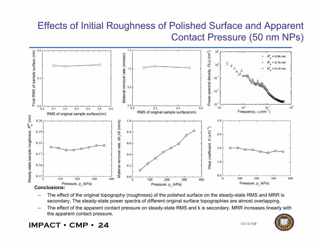
Effects of Initial Roughness of Polished Surface and ApparentContact Pressure (50 nm NPs)
Conclusions:– The effect of the original topography (roughness) of the polished surface on the steady-state RMS and MRR is
secondary. The steady-state power spectra of different original surface topographies are almost overlapping.– The effect of the apparent contact pressure on steady-state RMS and k is secondary. MRR increases linearly with
the apparent contact pressure.
IMPACT • CMP • 25 10/2/09
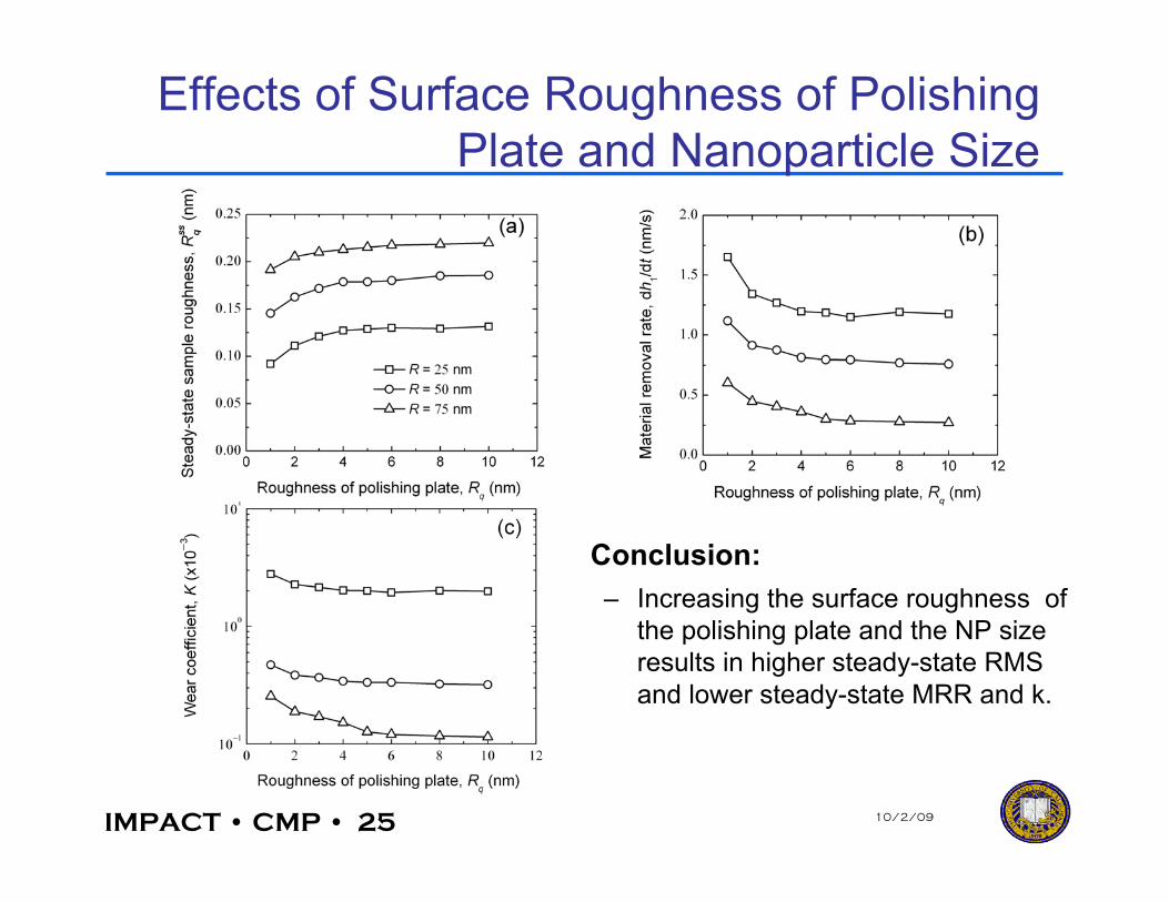
Effects of Surface Roughness of PolishingPlate and Nanoparticle Size
Conclusion:– Increasing the surface roughness of
the polishing plate and the NP sizeresults in higher steady-state RMSand lower steady-state MRR and k.
IMPACT • CMP • 26 10/2/09
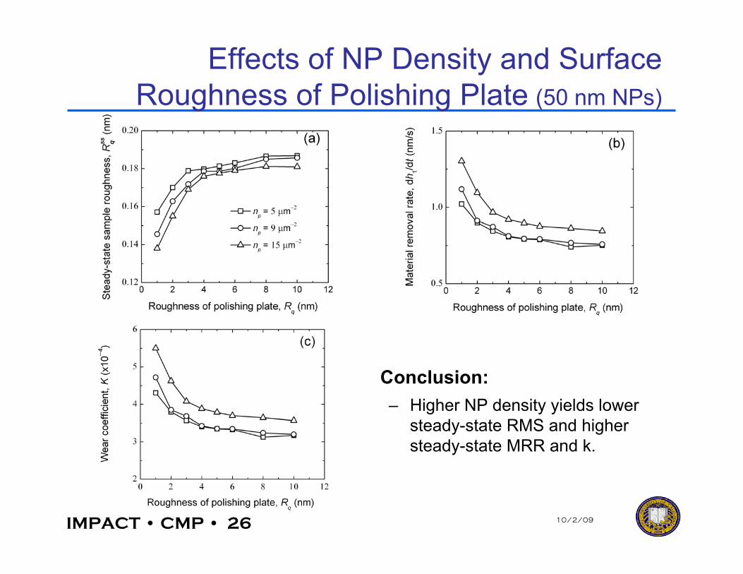
Effects of NP Density and SurfaceRoughness of Polishing Plate (50 nm NPs)
Conclusion:– Higher NP density yields lower
steady-state RMS and highersteady-state MRR and k.
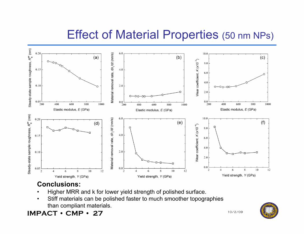
IMPACT • CMP • 27 10/2/09
Effect of Material Properties (50 nm NPs)
Conclusions:• Higher MRR and k for lower yield strength of polished surface.• Stiff materials can be polished faster to much smoother topographies
than compliant materials.
IMPACT • CMP • 28 10/2/09
Future Goals Slip-line plasticity analysis and FEM modeling of a single NP
removing material from the polished surface (analysis of materialremoval at the NP level).
FEM analysis of material removal at the NP scale (a fracturemechanics approach).
Nanoscale polishing mechanics studied by nanoscratchingexperiments involving diamond tips of different size/shape anddifferent contact loads.
Friction coefficient measurements and lubricant chemistry effect onMRR and material transfer to the polishing plate surface (modelextension from mechanical to chemomechanical polishing).
Nanoscale polishing experiments under different loads and speedswith glycol and other hydrocarbon-based lubricants (study of chemicaleffects on nanoscale polishing).
IMPACT • CMP • 29 10/2/09
Objective
Complete the comprehensive model of CMP for homogeneoussubstrate, and start adapting this to account for patterndependence– Complete the model that links mechanical and electrochemical
characteristics using millisecond-scale protective film formation kinetics.– Numerically implement the tribo-chemical model of copper CMP and
verify the validity of the model.– Draw on abrasive-scale and pattern-scale capabilities to extend the
model to DfM applications.
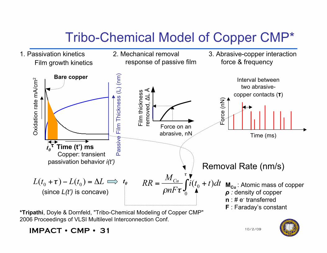
Investigation of Validity of Tribo-Chemical Model of Copper CMP in Acidic Polishing Slurries
IMPACT • CMP • 30 10/2/09
Problem
The interval between consecutive copper and asperities/abrasivesinteractions is important in determining the amount of protective filmon copper surface during copper CMP.
The asperities of most conventional CMP pads are randomlydistributed, and thus their interaction with copper during copperCMP is also randomized.
A fixed abrasive pad has been adopted to provide a defined intervalbetween consecutive copper and asperities/abrasives interactions,but these have a much larger geometric scale than conventionalCMP pads, which makes it less effective in simulating copper CMPoperation, where millisecond-scale interactions dominate behavior.
The oxidation rate of copper in a solution whose potential iscontrolled by an oxidizer (i.e. H2O2) is hard to compare withchronoamperometry data because of passivation of copper when alarge amount of oxidizer is present.
IMPACT • CMP • 31 10/2/09
Tribo-Chemical Model of Copper CMP*O
xida
tion
rate
mA
/cm
2 Bare copper
Time (t’) msCopper: transient
passivation behavior i(t’)
Pas
sive
Film
Thi
ckne
ss (L
) (nm
)
1. Passivation kineticsFilm growth kinetics
Interval betweentwo abrasive-
copper contacts (τ)
Time (ms)
Forc
e (n
N)
Force on anabrasive, nN
Film
thic
knes
sre
mov
ed, Δ
L Å
t0
τ
! +=
"
"#0
0 )( dtttinF
MRR
Cu
Removal Rate (nm/s)
τ
MCu : Atomic mass of copperρ : density of coppern : # e- transferredF : Faraday’s constant
*Tripathi, Doyle & Dornfeld, "Tribo-Chemical Modeling of Copper CMP"2006 Proceedings of VLSI Multilevel Interconnection Conf.
3. Abrasive-copper interactionforce & frequency
2. Mechanical removalresponse of passive film
LtLtL !="+ )()( 00 # t0(since L(t’) is concave)
IMPACT • CMP • 32 10/2/09
11/02/2009
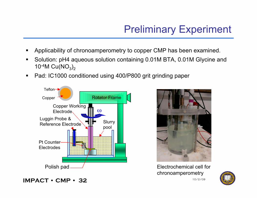
Preliminary Experiment
Applicability of chronoamperometry to copper CMP has been examined. Solution: pH4 aqueous solution containing 0.01M BTA, 0.01M Glycine and
10-4M Cu(NO3)2
Pad: IC1000 conditioned using 400/P800 grit grinding paper
Electrochemical cell forchronoamperometry
Pt CounterElectrodes
Luggin Probe & Reference Electrode
Polish pad
Copper WorkingElectrode
Slurrypool
Rotator Frame
ω
Teflon
Copper
IMPACT • CMP • 33 10/2/09
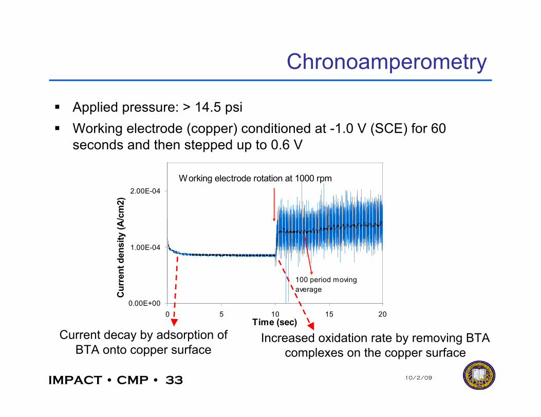
Chronoamperometry
Applied pressure: > 14.5 psi Working electrode (copper) conditioned at -1.0 V (SCE) for 60
seconds and then stepped up to 0.6 V
0.00E+00
1.00E-04
2.00E-04
0 5 10 15 20
Time (sec)
Cu
rren
t d
en
sit
y (
A/c
m2)
Working electrode rotation at 1000 rpm
100 period moving
average
Current decay by adsorption ofBTA onto copper surface
Increased oxidation rate by removing BTAcomplexes on the copper surface
IMPACT • CMP • 34 10/2/09
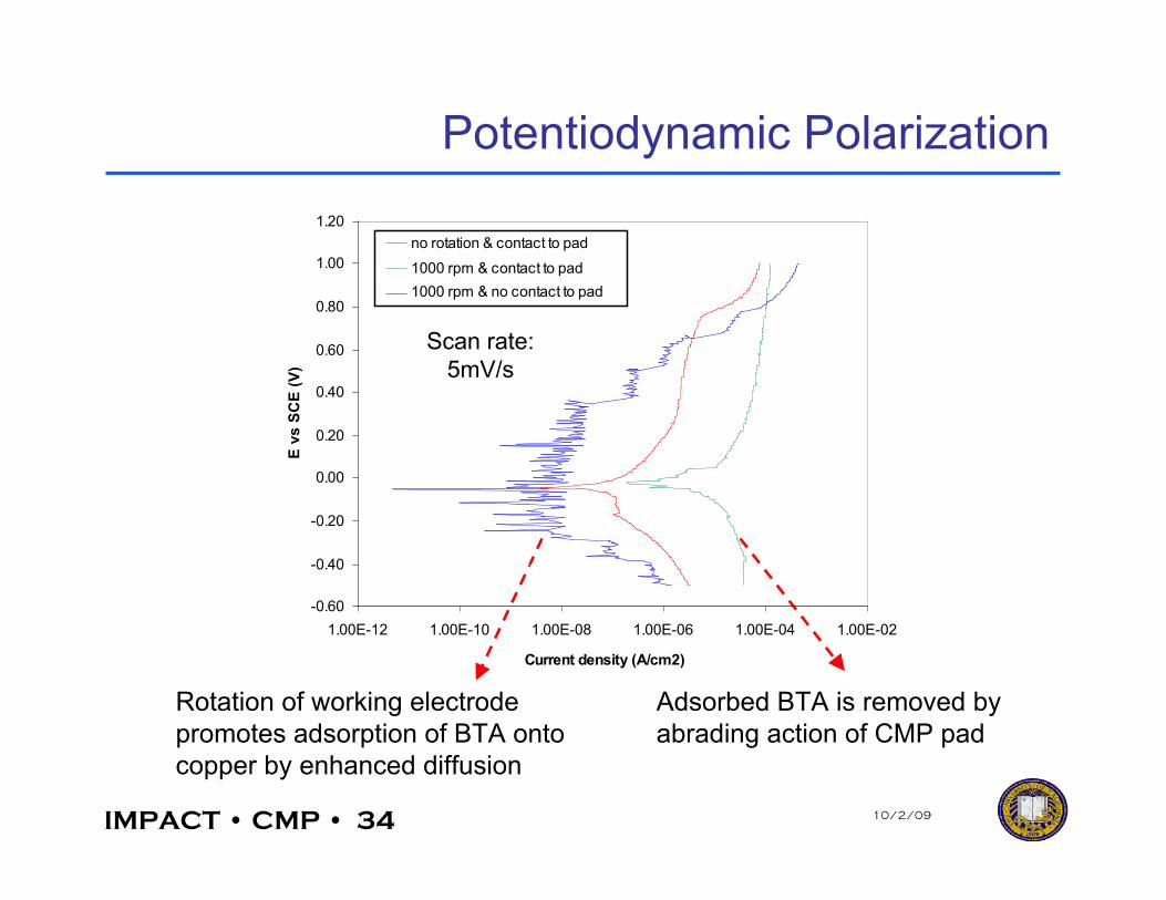
Potentiodynamic Polarization
Rotation of working electrodepromotes adsorption of BTA ontocopper by enhanced diffusion
Scan rate:5mV/s
Adsorbed BTA is removed byabrading action of CMP pad
-0.60
-0.40
-0.20
0.00
0.20
0.40
0.60
0.80
1.00
1.20
1.00E-12 1.00E-10 1.00E-08 1.00E-06 1.00E-04 1.00E-02
Current density (A/cm2)
E v
s S
CE
(V
)
no rotation & contact to pad
1000 rpm & contact to pad
1000 rpm & no contact to pad
IMPACT • CMP • 35 10/2/09
Shortcomings of prototype, and remedial strategies
Very low MRR (circa 3 nm/min assuming Cu(II) oxidation state)– Mainly due to no abrasives being involved
→Need to use abrasives for higher removal rates– Material removal occurred mostly at outer region of the copper
electrode because of low linear velocity at inner region→Electrode is being modified to use a rotating ring electrode to achieverelatively uniform linear velocity distribution along the radial direction of theelectrode. Will also lower Ohmic resistance encountered by current.
Uncertainty on applied pressure and rotational speed of workingelectrode (which changes with applied pressure)
→Transducers to be installed to measure pressure, strobe tachometer to beused to measure rotational speed accurately
Noisy signal→Securely fix reference and counter electrodes so as to minimize vibration byrotation of copper electrode
IMPACT • CMP • 36 10/2/09
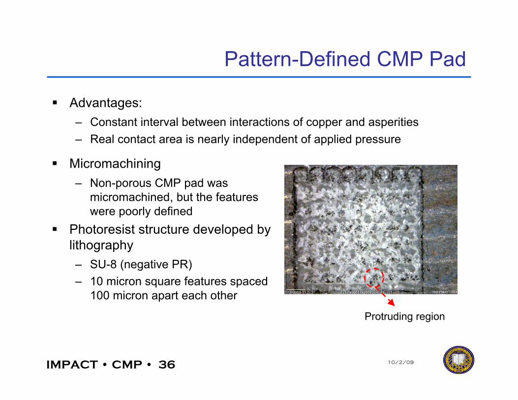
Pattern-Defined CMP Pad
Advantages:– Constant interval between interactions of copper and asperities– Real contact area is nearly independent of applied pressure
Micromachining– Non-porous CMP pad was
micromachined, but the featureswere poorly defined
Photoresist structure developed bylithography– SU-8 (negative PR)– 10 micron square features spaced
100 micron apart each other
Protruding region
IMPACT • CMP • 37 10/2/09
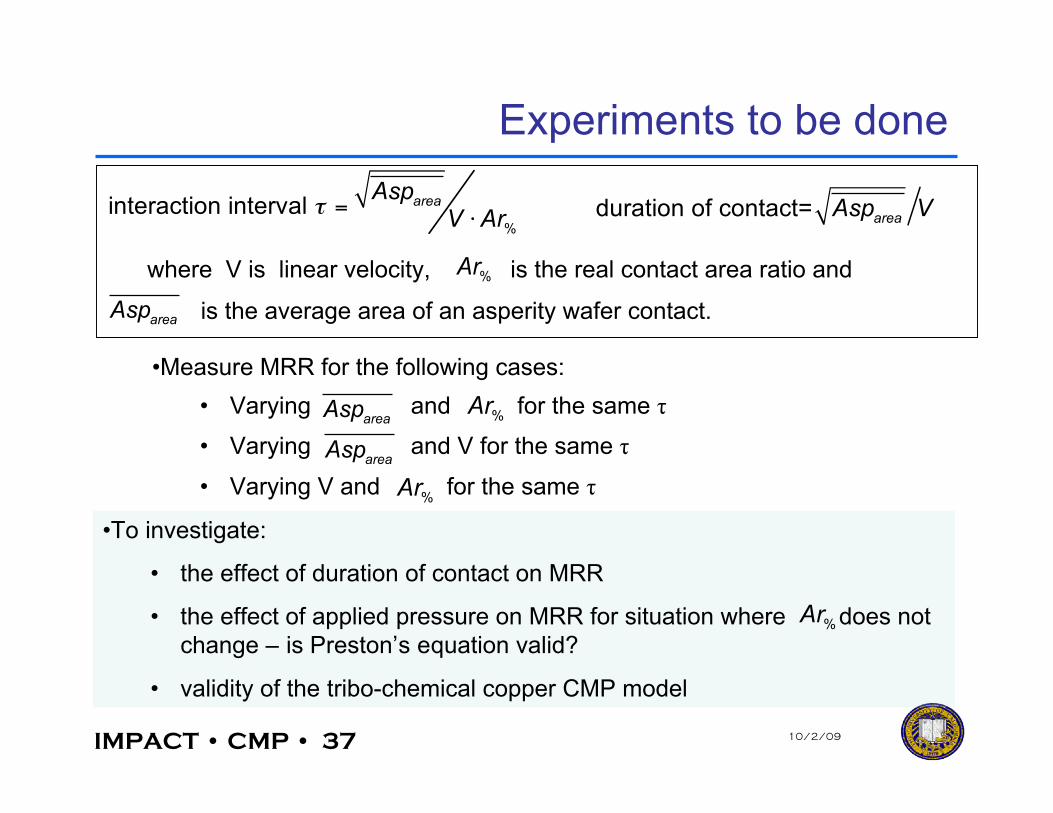
Experiments to be done
where V is linear velocity, is the real contact area ratio and
! ="
%
interaction interval areaAsp
V Ar duration of contact=area
Asp V
%Ar
areaAsp is the average area of an asperity wafer contact.
•Measure MRR for the following cases:• Varying and for the same τ
• Varying and V for the same τ
• Varying V and for the same τ
areaAsp
areaAsp
%Ar
%Ar
•To investigate:
• the effect of duration of contact on MRR
• the effect of applied pressure on MRR for situation where does notchange – is Preston’s equation valid?
• validity of the tribo-chemical copper CMP model
%Ar
IMPACT • CMP • 38 10/2/0911/02/2009
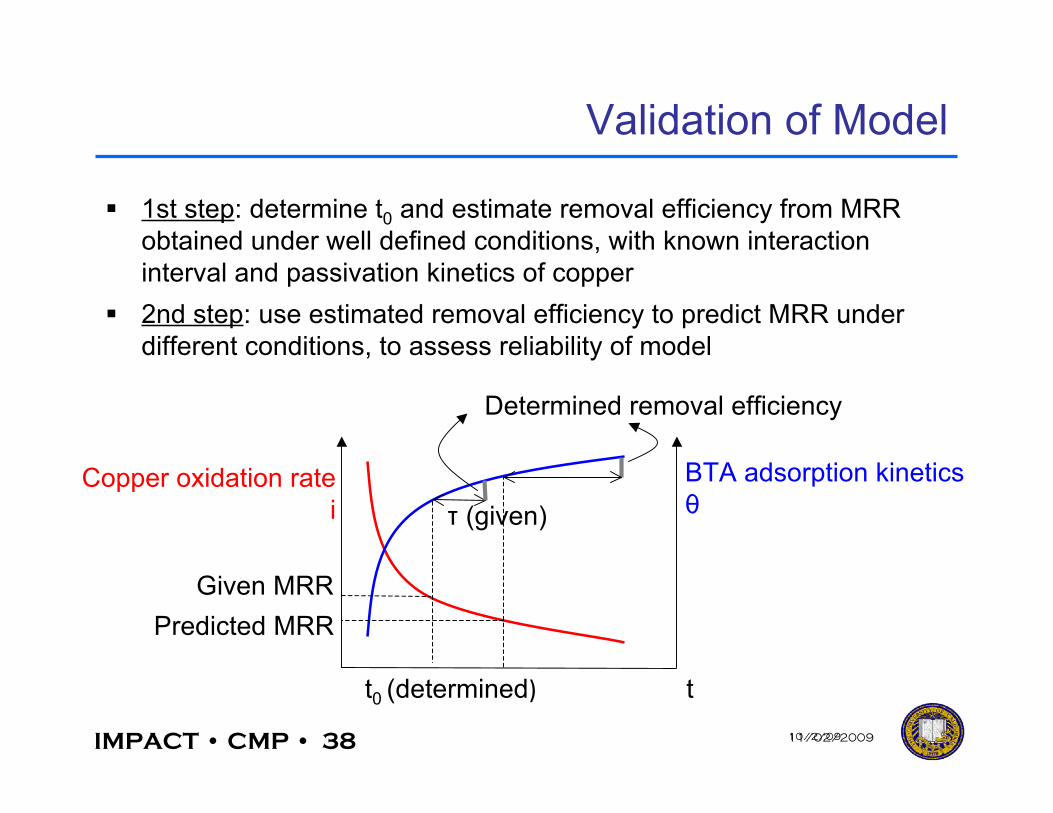
Validation of Model
1st step: determine t0 and estimate removal efficiency from MRRobtained under well defined conditions, with known interactioninterval and passivation kinetics of copper
2nd step: use estimated removal efficiency to predict MRR underdifferent conditions, to assess reliability of model
Copper oxidation ratei
t
BTA adsorption kineticsθτ (given)
t0 (determined)
Given MRR
Determined removal efficiency
Predicted MRR
IMPACT • CMP • 39 10/2/09
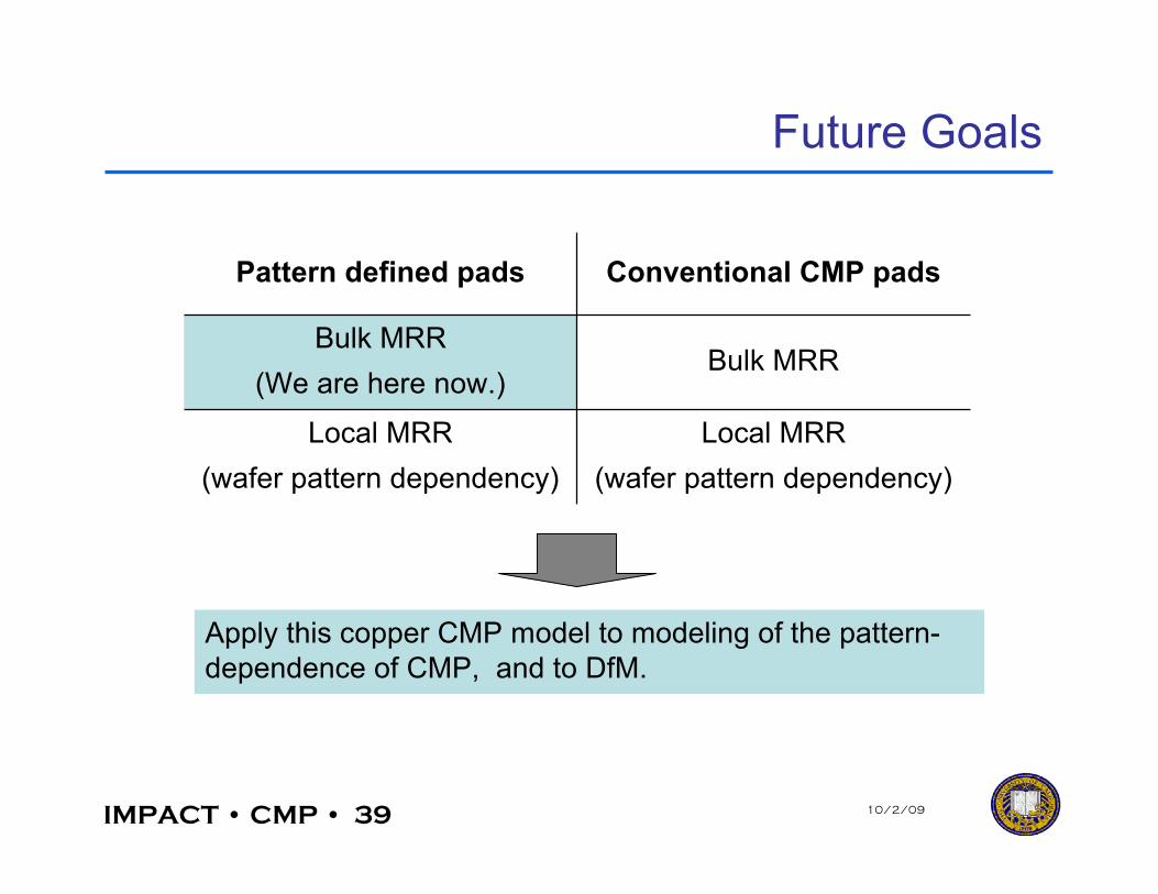
Future Goals
Pattern defined pads Conventional CMP pads
Bulk MRR(We are here now.)
Bulk MRR
Local MRR(wafer pattern dependency)
Local MRR(wafer pattern dependency)
Apply this copper CMP model to modeling of the pattern-dependence of CMP, and to DfM.
IMPACT • CMP • 40 10/2/09
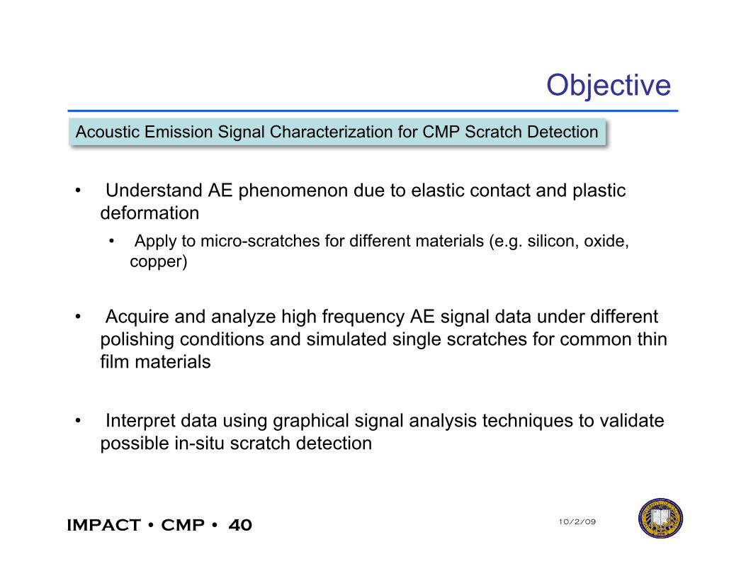
Objective
• Understand AE phenomenon due to elastic contact and plasticdeformation• Apply to micro-scratches for different materials (e.g. silicon, oxide,
copper)
• Acquire and analyze high frequency AE signal data under differentpolishing conditions and simulated single scratches for common thinfilm materials
• Interpret data using graphical signal analysis techniques to validatepossible in-situ scratch detection
Acoustic Emission Signal Characterization for CMP Scratch Detection
IMPACT • CMP • 41 10/2/09
The Problem
• Scratch detection done ex-situ, typically visual, after processing a batch ofwafers• many wafers may be scratched before detection• visual inspection/monitoring decreases throughput
• Traditional sensor and monitoring methods not precision or robust enoughto detect micro-scratching; either too global (averaging), or too local (pointdetection)• difficult to distinguish between scratch and “normal” abrasion process
• Detecting energy alone is not enough!
Use AE to extract material signature and/or frequency pattern
IMPACT • CMP • 42 10/2/09
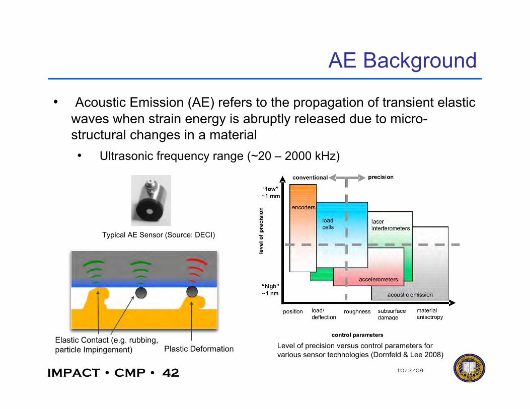
AE Background
• Acoustic Emission (AE) refers to the propagation of transient elasticwaves when strain energy is abruptly released due to micro-structural changes in a material• Ultrasonic frequency range (~20 – 2000 kHz)
Plastic DeformationElastic Contact (e.g. rubbing, particle Impingement) Level of precision versus control parameters for
various sensor technologies (Dornfeld & Lee 2008)
Typical AE Sensor (Source: DECI)
IMPACT • CMP • 43 10/2/09
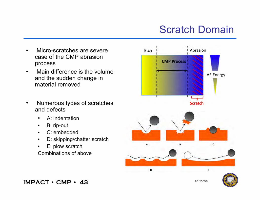
Scratch Domain
• Micro-scratches are severecase of the CMP abrasionprocess
• Main difference is the volumeand the sudden change inmaterial removed
• Numerous types of scratchesand defects• A: indentation• B: rip-out• C: embedded• D: skipping/chatter scratch• E: plow scratchCombinations of above
IMPACT • CMP • 44 10/2/09
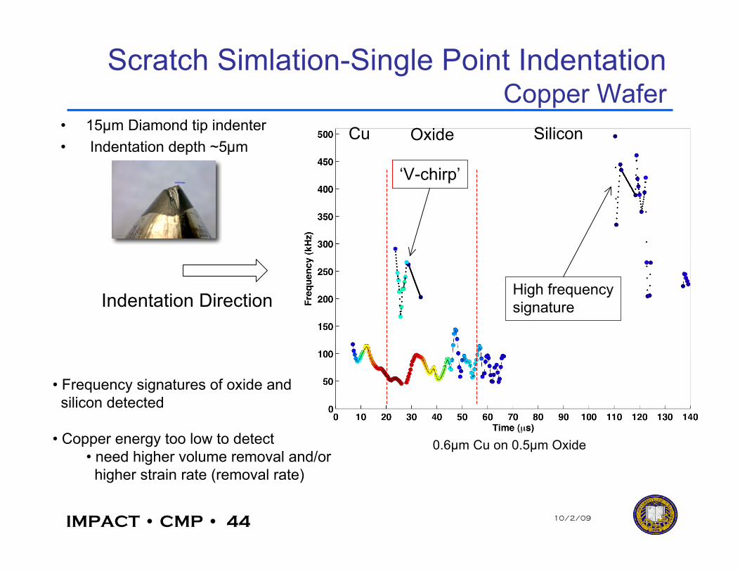
Scratch Simlation-Single Point IndentationCopper Wafer
SiliconOxide
‘V-chirp’
High frequencysignature
0.6µm Cu on 0.5µm Oxide
Cu
Indentation Direction
• Frequency signatures of oxide and silicon detected
• Copper energy too low to detect• need higher volume removal and/or higher strain rate (removal rate)
• 15µm Diamond tip indenter• Indentation depth ~5µm
IMPACT • CMP • 45 10/2/09
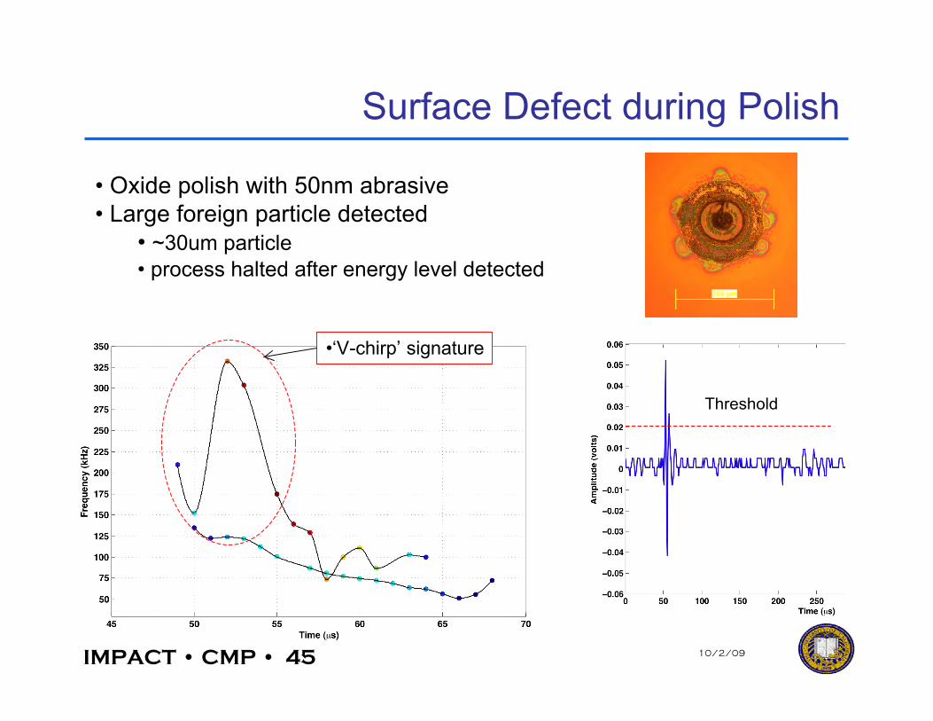
Surface Defect during Polish
•‘V-chirp’ signature
• Oxide polish with 50nm abrasive• Large foreign particle detected
• ~30um particle• process halted after energy level detected
Threshold
IMPACT • CMP • 46 10/2/09
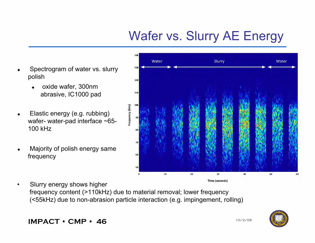
Wafer vs. Slurry AE Energy
• Slurry energy shows higher frequency content (>110kHz) due to material removal; lower frequency (<55kHz) due to non-abrasion particle interaction (e.g. impingement, rolling)
Spectrogram of water vs. slurrypolish
oxide wafer, 300nmabrasive, IC1000 pad
Elastic energy (e.g. rubbing)wafer- water-pad interface ~65-100 kHz
Majority of polish energy samefrequency
IMPACT • CMP • 47 10/2/09
Conclusion• High frequency AE signatures exists in silicon and oxide
• silicon and oxide show higher AE energy than copper• macro scratches detectable through the oxide
• Advance signal processing techniques and hardware needed to extractand analyze AE signal
• large computations may be reduced once AE scratch signals arefully characterized
• High frequency AE signature for copper (metals) may exist• need higher sensitivity AE sensors and higher signal-to-noise ratioamplifiers to detect copper removal
AE is a viable sensor technology for in-situ scratch and defectdetection
IMPACT • CMP • 48 10/2/09
Future Goals
• More precision signal characterization, focusing on copper detectionand continuous AE signature extraction
• Investigate the detection of different wave types (e.g. lamb, Rayleigh,etc…) for more unique scratch behavior
• Develop a relatively low delay micro-scratch monitoring system• Implement an integrated feedback using adaptive signalprocessing (e.g. least mean squared algorithm)
• Develop wireless AE setup for full CMP integration
IMPACT • CMP • 49 10/2/09
Objectives
Characterization of a conventional pad
The analysis of structural effects
The fabrication of prototype pads using micro molding technology for bettertesting, validation, and comparison with conventional pad
Study on of various CMP performance vs. pad designs shows improvedMRR, reduced dishing and erosion
Development of Micro-Structure Pad in CMP Process and Evaluating the Effects on Planarization
IMPACT • CMP • 50 10/2/09
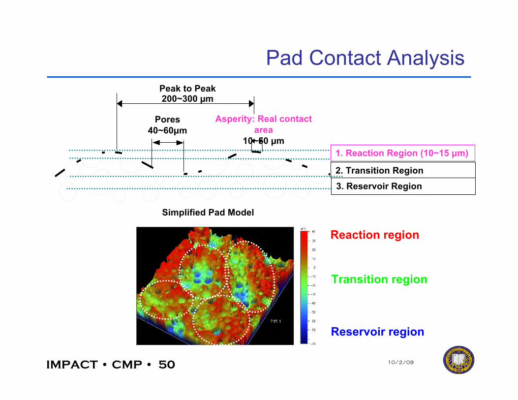
Pad Contact Analysis
Simplified Pad Model
Asperity: Real contactarea
10~50 µm
Pores40~60µm
Peak to Peak200~300 µm
1. Reaction Region (10~15 µm)
2. Transition Region3. Reservoir Region
Reaction region
Reservoir region
Transition region
IMPACT • CMP • 51 10/2/09
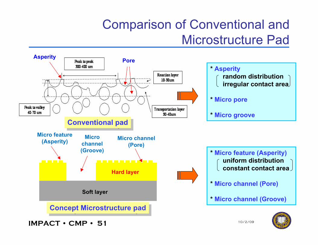
Asperity Pore
Conventional padConventional pad
* Micro feature (Asperity) uniform distribution constant contact area
* Micro channel (Pore)
* Micro channel (Groove)
* Asperity random distribution irregular contact area
* Micro pore
* Micro groove
Concept Microstructure padConcept Microstructure pad
Soft layer
Hard layer
Micro feature(Asperity) Micro channel
(Pore)Micro
channel(Groove)
Comparison of Conventional andMicrostructure Pad
IMPACT • CMP • 52 10/2/09
Future Goals
The fabrication of completed Microstructure pad using micro-moldingtechnology
STI CMP performances using the Microstructure pad• Pattern selectivity
• Effect of defects such as nitride erosion, corner rounding and oxidedishing
Accomplishment of planarization within wafer
Survey of materials and design concept
Other applications: metal CMP (Cu, W)