2008 Advanced Materials Characterization Workshop · 2008 Advanced Materials Characterization...
28
1 2008 Advanced Materials Characterization Workshop Mt il h t i ti Sponsors: The Frederick Seitz Materials Research Laboratory University of Illinois at Urbana-Champaign Materials characterization: the need for complementary techniques Ivan Petrov 1 Sponsors: Supported by the U.S. Department of Energy under grants DEFG02-07-ER46453 and DEFG02-07-ER46471 © 2008 University of Illinois Board of Trustees. All rights reserved. Why materials analysis Material characterization at the atomic scale is needed: needed: • In order to understand/control the synthesis processes • In order to understand why materials, micro-, and nanosystems work or fail Understand 2 Understand synthesis – structure/composition – properties relationship
Transcript of 2008 Advanced Materials Characterization Workshop · 2008 Advanced Materials Characterization...
1
2008 Advanced Materials Characterization Workshop
M t i l h t i ti
Sponsors:
The Frederick Seitz Materials Research LaboratoryUniversity of Illinois at Urbana-Champaign
Materials characterization: the need for complementary techniques
Ivan Petrov
1
Sponsors:
Supported by the U.S. Department of Energy under grants DEFG02-07-ER46453 and DEFG02-07-ER46471© 2008 University of Illinois Board of Trustees. All rights reserved.
Why materials analysis
Material characterization at the atomic scale is needed:needed:
• In order to understand/control the synthesis processes• In order to understand why materials, micro-, and
nanosystems work or fail
Understand
2
Understand synthesis – structure/composition – properties relationship
2
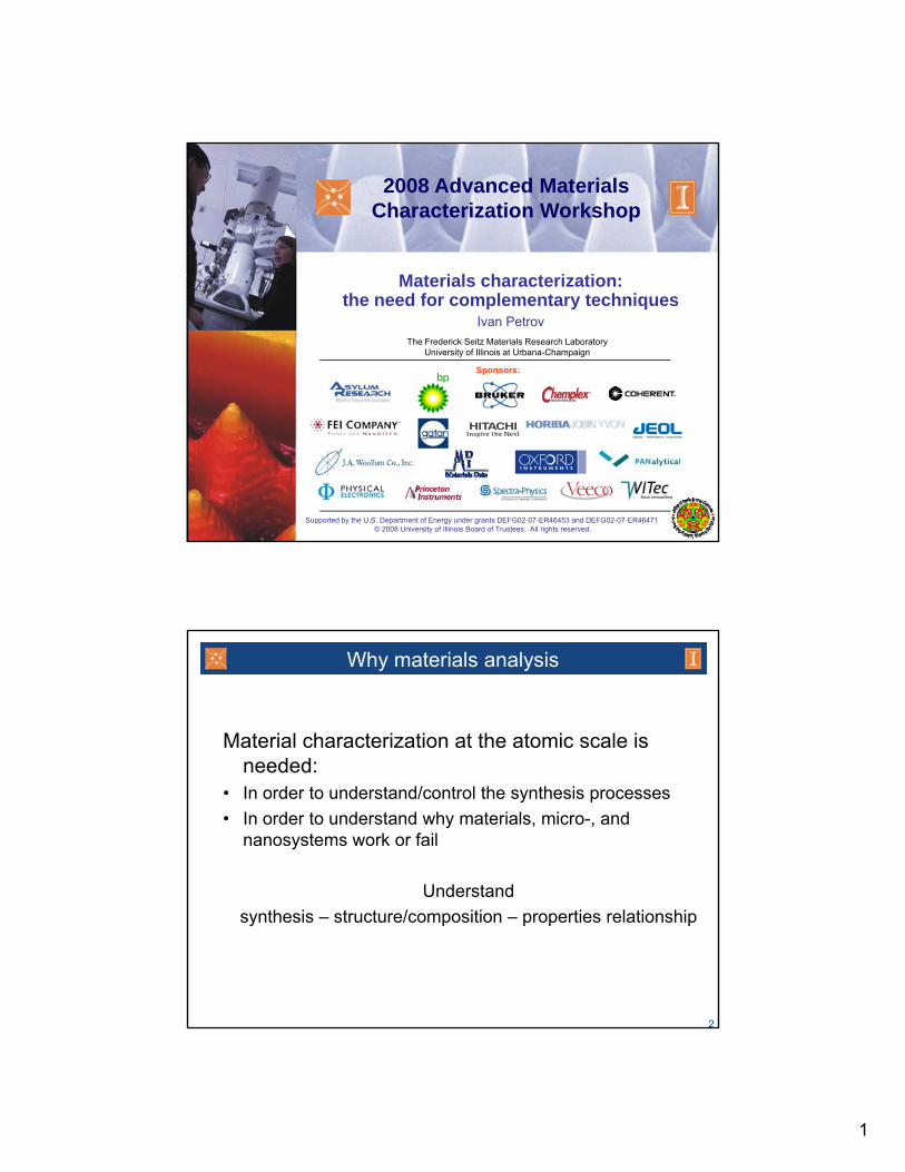
Main questions to answer
1. What are the building blocks – elemental and chemical analysis
2. What is the electronic structure3. What is the arrangement of the building blocks –
crystallographic analysis4. What are the surface morphology and bulk
nanostructure – imaging from micron to sub-nanometer scale
3
nanometer scale
IonsElectrons
IonsElectrons
Primary beam (source, gun)
Secondary beam (spectrometers, detectors)
Wide variety of methods for materials analysis
ElectronsPhotons
ElectronsPhotons
4
* with ions and electrons: the sample is in vacuum** exception: scanning probe microscopy
3
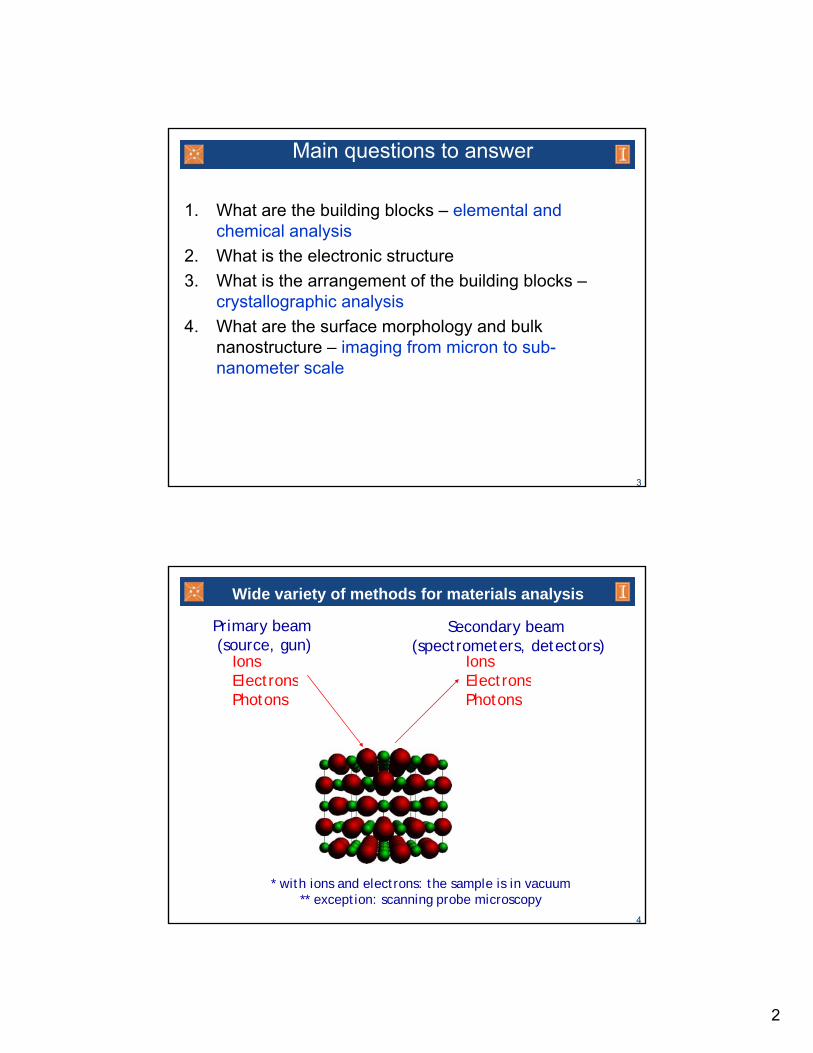
5
http://www.eaglabs.com/
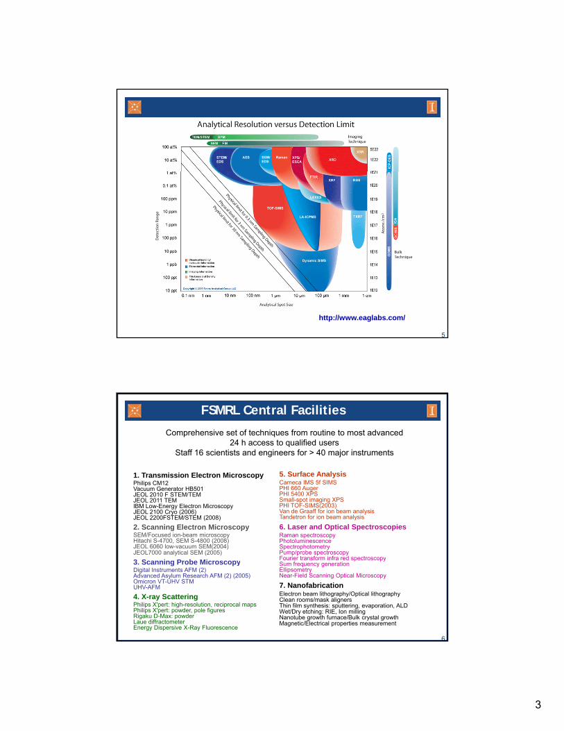
FSMRL Central Facilities
Comprehensive set of techniques from routine to most advanced24 h access to qualified users
Staff 16 scientists and engineers for > 40 major instruments
5. Surface Analysis1 Transmission Electron Microscopy 5. Surface AnalysisCameca IMS 5f SIMSPHI 660 AugerPHI 5400 XPSSmall-spot imaging XPSPHI TOF-SIMS(2003)Van de Graaff for ion beam analysisTandetron for ion beam analysis
6. Laser and Optical SpectroscopiesRaman spectroscopyPhotoluminescenceSpectrophotometryPump/probe spectroscopyFourier transform infra red spectroscopy
1. Transmission Electron MicroscopyPhilips CM12Vacuum Generator HB501JEOL 2010 F STEM/TEMJEOL 2011 TEMIBM Low-Energy Electron MicroscopyJEOL 2100 Cryo (2006)JEOL 2200FSTEM/STEM (2008)2. Scanning Electron MicroscopySEM/Focused ion-beam microscopyHitachi S-4700, SEM S-4800 (2008)JEOL 6060 low-vacuum SEM(2004)JEOL7000 analytical SEM (2005)
6
Fourier transform infra red spectroscopySum frequency generation EllipsometryNear-Field Scanning Optical Microscopy
7. NanofabricationElectron beam lithography/Optical lithographyClean rooms/mask alignersThin film synthesis: sputtering, evaporation, ALDWet/Dry etching: RIE, Ion millingNanotube growth furnace/Bulk crystal growthMagnetic/Electrical properties measurement
3. Scanning Probe MicroscopyDigital Instruments AFM (2) Advanced Asylum Research AFM (2) (2005)Omicron VT-UHV STMUHV-AFM4. X-ray ScatteringPhilips X'pert: high-resolution, reciprocal maps Philips X'pert: powder, pole figuresRigaku D-Max: powderLaue diffractometerEnergy Dispersive X-Ray Fluorescence

4
interaction with ANL:High-power lithium-ion battery failure mechanisms
A comprehensive characterization approach
0.5 μm
0.5 μm
Aged
0
1000
2000
3000
4000
5000
6000
7000
8000
682 683 684 685 686 687 688 689 690 691 692
Binding energy, eV
LiF
-(CF2-CH2)n-XPS, F1s spectrum50C, 60% SOC, 16 wk test
0
1000
2000
3000
4000
5000
6000
7000
8000
282 283 284 285 286 287 288 289 290 291 292 293 294
Binding Energy, eV
graphite
-(CF2-CH2)n--(CF2-CH2)n-
-(CH2)n-
-C-O-
-OCO2-
XPS, C1s spectrumPositive electrode50C, 60% SOC, 16 wk test
-C=O
-O-C=O
Imaging Spectroscopy (XPS) Elemental analysis
HRTEM Crystallography and EELS
X-ray structure
refinement
C Li
Ni All
Fresh
7
20 nm
530 535 540 545 550 555 560 565 570 575 580 585 590eV
0.00
0.01
0.02
0.03
0.04
0.05
0.06
0.07
0.08
0.09
0.10
0.11
µm
850 860 870 880 890 900 910eV
0.00
0.02
0.04
0.06
0.08
0.10
µm
Bulk
Bulk O K-edge
Ni L-edge
Particle Surface
HRTEM, Crystallography, and EELS
(006)(113)
(110)
(018)(107)(015)
(104)
(012)
(101)
C(002)
(003)
Inte
nsity
(a.u
.)
2-theta (o)
f
nbeam[beam particles cm-
3]
Beam Flux: Jbeam= nbeamv [beam particles cm-2s-1]
Scattering cross section – one target atom
v – beam particle velocity
vΔtσ=π r2
V = vΔtσ
] p y
8
Nevents= nbeamV = nbeamvΔtσ = JbeamσΔt
σ = Nevents_per-seccond/Jbeam
5
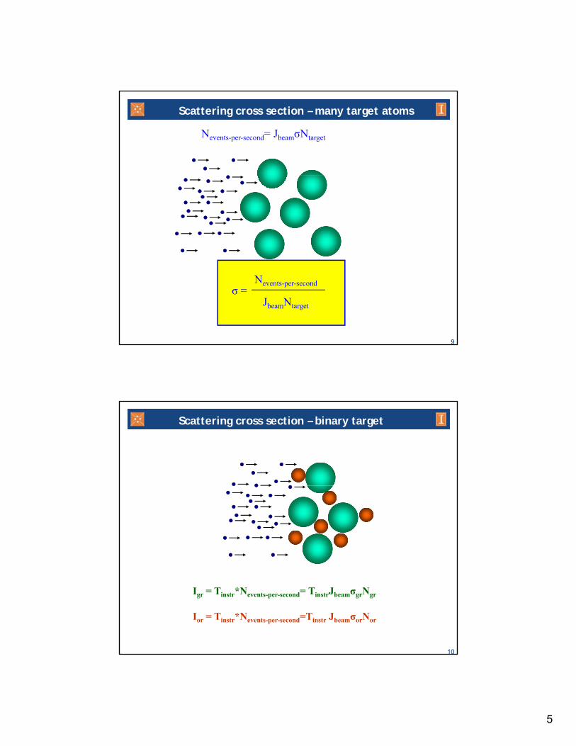
Nevents-per-second= JbeamσNtarget
Scattering cross section – many target atoms
9
σ = Nevents-per-second
JbeamNtarget
Scattering cross section – binary target
10
Igr = Tinstr*Nevents-per-second= TinstrJbeamσgrNgr
Ior = Tinstr*Nevents-per-second=Tinstr JbeamσorNor

6
σ=π r2
Δt
Mean free path
vΔt V = vΔtσ
Nevents= ntargetV = ntargetvΔtσ
T l d di t Δt
11
λ = 1/ σ ntarget (cm/events)
Mean free path = Traveled distance
Number of events=
vΔt
ntargetvΔtσ
Scattering cross-section - σ
σ – probability that a scattering process occurs
σ = N/Jbeamntarget (events/beam particle/(atom/cm2))
N – number of events of certain type per sec (elastic, inner shell ionization, etc)Jbeam – particle beam flux (particles/sec/cm2)ntarget – target atom density (atoms/cm3)
λ – mean free path
12
λ = 1/ σ ntarget (cm/events)
If several different scattering processes can occur (λi)
1/λtotal = Σ(1/λi)

7
Beam particles properties
0.0122
13
X-ray/Matter InteractionsCoherent scattering
hν0
hν0hν1
Fluorescence
hν2 Photoelectrone-
Incoherent scattering
Incident x-ray photons XRD
XRF
XPSAuger electrone-
Coherent scattering (Thompson scattering / diffraction): incident photon hνo interacts with e- with no energy loss and no phase change
Incoherent scattering (Compton scattering): (a) e- absorbes incident energy hνo (excited photoelectron); (b) part of the energy is emitted at different energy hν1 and different phase.
50 μm – 5 cm
5 μm
Sample
Interactionvolume hν: photon
e-: electron
14
( ) p gy gy 1 p
Fluorescence (Characteristic x-rays): (a) K/L shell e- absorb incident energy hνo; (b) outer shell e-“cascade” down filling the “holes” causing secondary photons emission (hν2).
Photoelectron emission: hν0 energy is used to eject electron e- with kinetic energy = hνo – B.E.(binding energy).
Auger electron emission: (a) incident hν0 used to eject e- from atom; (b) 2nd e- “falls” to lower levels to fill the “hole”and a photon is
emitted; (c) the emitted photon is absorbed by valance e-, which ionizes and leaves the atom.
8
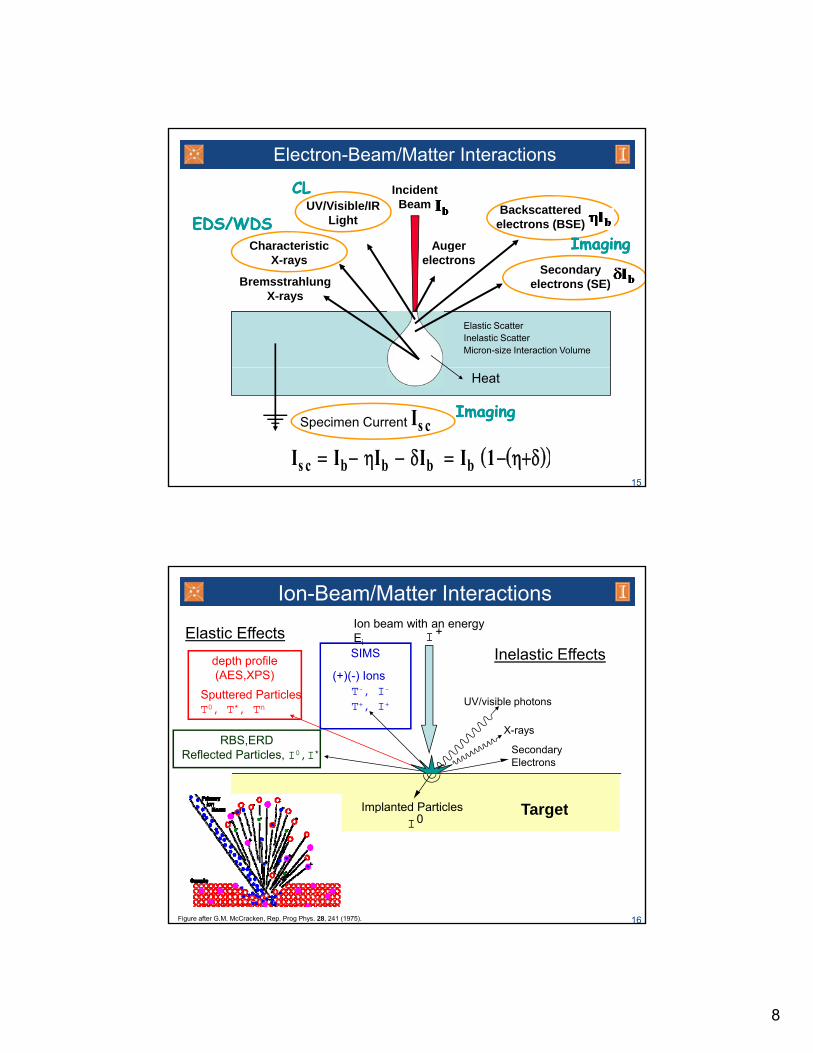
Electron-Beam/Matter Interactions
IncidentBeam
Characteristic
UV/Visible/IR Light
AugerEDS/WDSEDS/WDS
ImagingImaging
CLCLBackscattered
electrons (BSE)
Secondary electrons (SE)
Characteristic X-rays
Bremsstrahlung X-rays
Auger electrons
ImagingImaging
Elastic ScatterInelastic ScatterMicron-size Interaction Volume
15
Heat
Specimen Current
Is c = Ib− ηIb − δIb = Ib (1−(η+δ))
ImagingImagingIs c
Ion-Beam/Matter Interactions
Inelastic Effects
Ion beam with an energy Ei
+IElastic Effects
(+)(-) Ions
SIMSdepth profile (AES,XPS)
Implanted Particles
UV/visible photons
X-rays
SecondaryElectrons
Sputtered ParticlesT0, T*, Tn
Reflected Particles, I0,I*
T+, I+
T t
T-, I-
RBS,ERD
16
Implanted ParticlesI0
Target
Figure after G.M. McCracken, Rep. Prog Phys. 28, 241 (1975).

9
What is the arrangement of the atoms in materials -crystallographic analysis
Answering question #3
usingelastic (coherent) electron and x-ray scatteringdiffraction analysis (reciprocal space mapping)
17
Coherent diffraction by a crystal
plane normal1 1’
Ki Kd
Plane wave(x-ray or electron)
θ
d sinθ
A
B
C
d
2 2’
Ki
d
KΨ = Ψoe2πx/λ
Ψ = Ψoe2πKx
18
2n d sinλ = θBragg’s Law: by definition wave vector |Ki,d| = 1/λ
scattering vector: |K|/2 = |Kd| sinθ
|K|= 2sinθ/ λ= 1/d
10
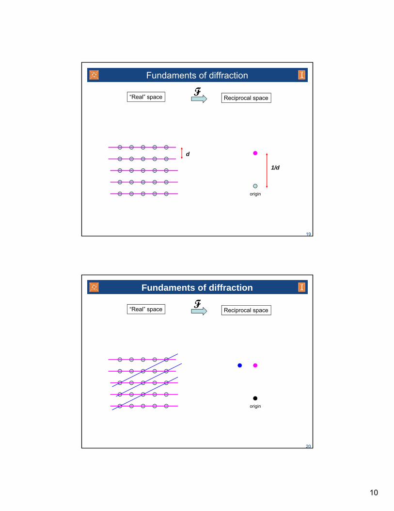
Fundaments of diffraction
“Real” space Reciprocal spaceF
d
1/d
19
origin
Fundaments of diffraction
“Real” space Reciprocal spaceF
20
origin
11
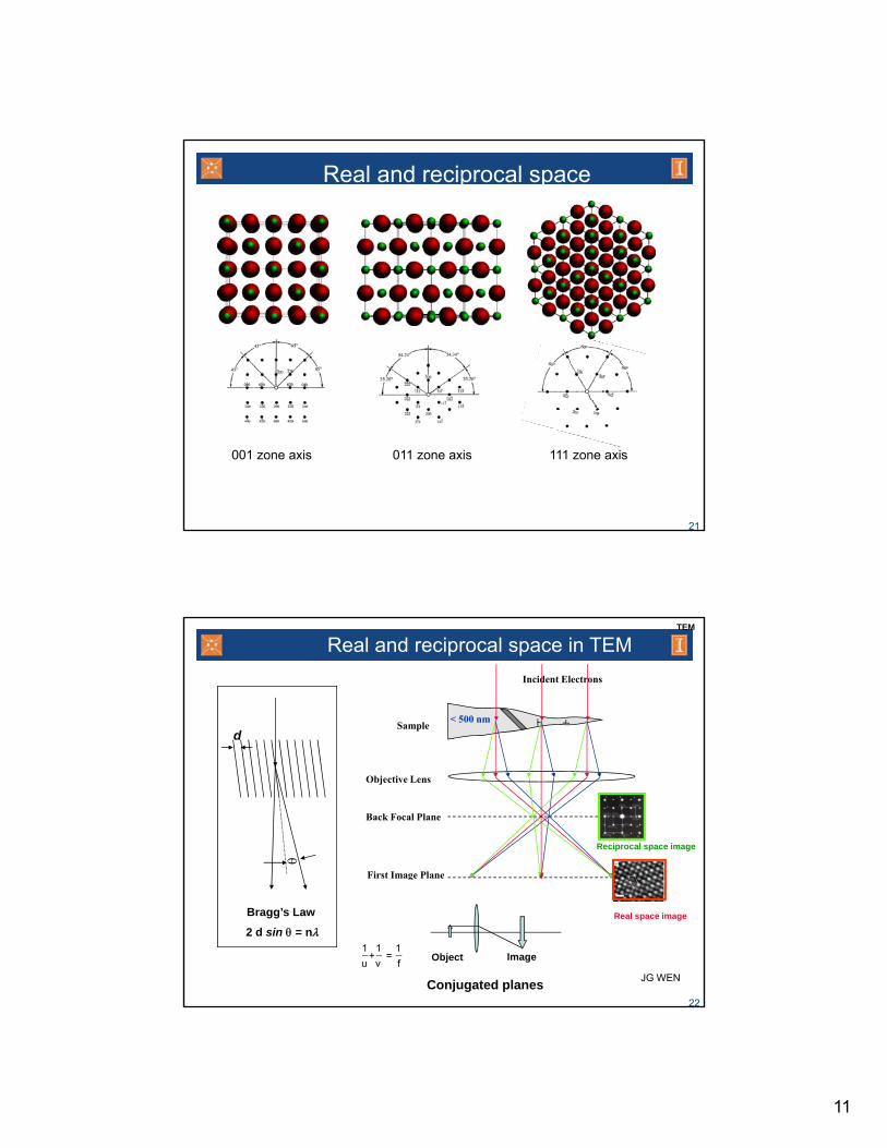
Real and reciprocal space
21
001 zone axis 011 zone axis 111 zone axis
Real and reciprocal space in TEMTEM
Sample
Incident Electrons
< 500 nm
d
Objective Lens
Back Focal Plane
First Image Plane
Reciprocal space image
θ
22
Conjugated planes
Object Image
First Image Plane
Real space image
u v f_ _ _+ =1 1 1
Bragg’s Law
2 d sin θ = nλ
JG WEN

12
Real and reciprocal space 022002
022
50 nm50 nm
23
001 zone axis 011 zone axis 111 zone axis
Selected-area electron diffractionExample of SAED and
dark-field imaging1) Selected-area Diffraction2) Nanobeam Diffraction3) Convergent-beam electron diffraction
Major Diffraction Techniques
Selected area apertureHigh-contrast
24
Selected-area apertureaperture
JG Wen

13
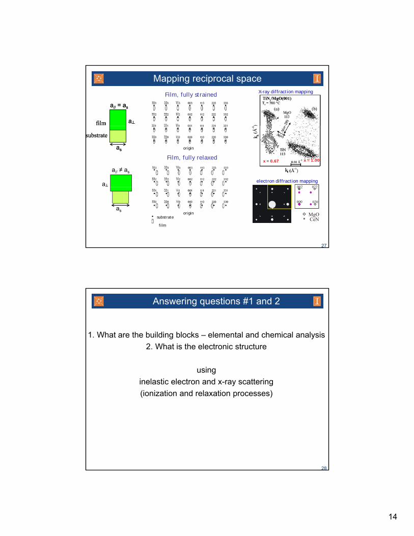
Mapping reciprocal spaceFilm, fully strained
film
a// = as
a┴film
a// = as
a┴
X-ray diffraction mapping
origin
Film, fully relaxed
022002electron diffraction mapping
x = 0.67 x = 1.00
substrate
as
substrate
as
a// ≠ as
a┴
25
originsubstrate
film
MgOCeN
000 020
022002
as
Instrumentation: high resolution configuration
ω
φ ψ
x-raysource
x-raymirror
slit
4-reflectionGe(220)
monochromator
ω
2θ
slit
Crossed slits(variable slit+mask)
3-bounceanalyzercrystal
Δθ =12 arc-secΔλ/λ = 5x10⁻⁵
X’Pert XRD #1High resolution
configuration with mirror and 4-reflections
26
“Upper” detector(open: < 1o acceptance)
“Lower” detector(triple axis: 12 arc-sec acceptance)
monochromator
Mauro Sardela
• Line focus;• Parabolic x-ray mirror;• 4-reflection monochromator (12 arc-sec resolution);
• Open detector or analyzer crystal.
Programmableattenuator
14
Mapping reciprocal spaceFilm, fully strained
film
a// = as
a┴film
a// = as
a┴
X-ray diffraction mapping
origin
Film, fully relaxed
022002electron diffraction mapping
x = 0.67 x = 1.00
substrate
as
substrate
as
a// ≠ as
a┴
27
originsubstrate
film
MgOCeN
000 020
022002
as
1. What are the building blocks – elemental and chemical analysis2. What is the electronic structure
Answering questions #1 and 2
2. What is the electronic structure
usinginelastic electron and x-ray scattering(ionization and relaxation processes)
28
15
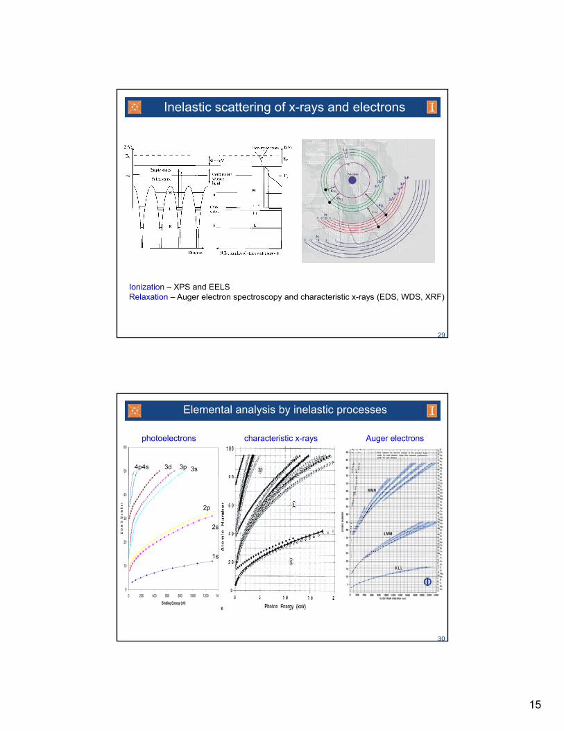
Inelastic scattering of x-rays and electrons
29
Ionization – XPS and EELSRelaxation – Auger electron spectroscopy and characteristic x-rays (EDS, WDS, XRF)
50
60
3s3p3d4s4p
Elemental analysis by inelastic processes
photoelectrons characteristic x-rays Auger electrons
20
30
40
Ato
mic
Num
ber
1s
2s
2p
30
0
10
0 200 400 600 800 1000 1200 1400
Binding Energy (eV)

16
Ionization
BE = hν (known) – KE(measured) BE = Eo(measured) – Eloss(measured)
S t t KE
Photoelectron Spectroscopy Electron Energy-Loss Spectroscopy
Conduction BandConduction Band
Valence Band
Fermi Level
Free Electron Level
Eincident X-ray = hν
Φ Conduction BandConduction Band
Valence Band
Eincident electron = Eo
Φ
Spectrometer, KE
31
1s
2s
2pBE
1s
2s
2pBE
Spectrometer, Eo, Eloss
Relaxation
Free Electron Level
Incident particle Ejected Electron Emitted Auger ElectronEmitted X-ray Photon
ionization
Conduction BandConduction Band
Valence Band
Fermi Level
2s
2p
Conduction Band
Valence Band
L2,L3
L1
32
1s K
KLL Auger electron
EAuger = E(K)- E(L2,3) - E(L2,3)
EX-ray = E(K) – E(L2,3)
17
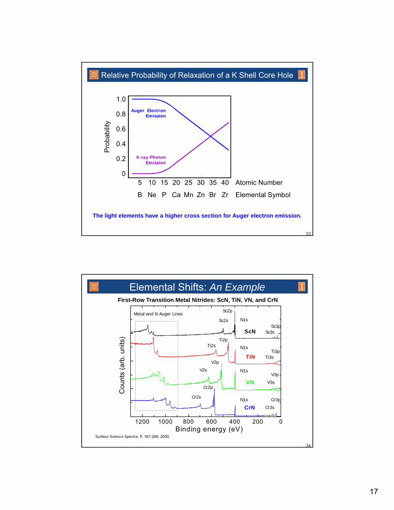
Relative Probability of Relaxation of a K Shell Core Hole
0.8
1.0Auger Electron
Emission
0
0.2
0.4
0.6
Prob
abili
ty
X-ray Photon Emission
33
5
B Ne P Ca Mn Zn Br Zr
10 15 20 25 30 35 40 Atomic Number
Elemental Symbol
The light elements have a higher cross section for Auger electron emission.
Elemental Shifts: An Example
ScN
Metal and N Auger LinesN1s
Sc2p
Sc2sSc3p
Sc3s
First-Row Transition Metal Nitrides: ScN, TiN, VN, and CrN
VN
TiN
ScN
Cou
nts
(arb
. uni
ts)
N1s
N1s
Ti2p
V2p
Cr2p
Ti2s
V2s
Sc3s
Ti3s
V3s
Ti3p
V3p
34
1200 1000 800 600 400 200 0
CrN
C
Binding energy (eV)
N1sCr2s
Cr3s
Cr3p
Surface Science Spectra, 7, 167-280, 2000.

18
1O primary e-beam0.5-30 keV
Scanning electron microscopy (SEM)primary e-beam
100-300 keV
Scanning transmissionelectron microscopy (STEM)
Elemental analysis by electron microscopySTEM
backscattered electrons
secondary electrons<50 eV
Auger electrons
characteristic &Bremsstrahlung x-rays
characteristic &Bremsstrahlung x-rays
Probe size 0.18 nm
Thickness
35
1 μm
“Coherent”Scattering
(i.e. Interference)
“Incoherent”Scattering
i.e. Rutherford
<100 nm
energy loss spectroscopy
Ion impact collision cascadeEnergy increasing (dependent on Mi/Mt)
Threshold regimerecoils sputtered, butno (limited) cascades
Linear cascadea series of binary collisions
Spike regimehigh density of recoils
36P.Sigmund, “Sputtering by ion bombardment: theoretical concepts”, in Sputtering by particle bombardment I, edited by R. Behrish, Springer-Verlag, 1981
• Ions striking a surface interact with a number of atoms in a series collisions; • recoiled target atoms in turn collide with atom at rest generating a collision cascade.• The initial ion energy and momentum are distributed to among the target recoil atoms. • When Ei > 1 keV, the cascade is “linear”, i.e. approximated by a series of binary collisions in a stationary matrix.
19
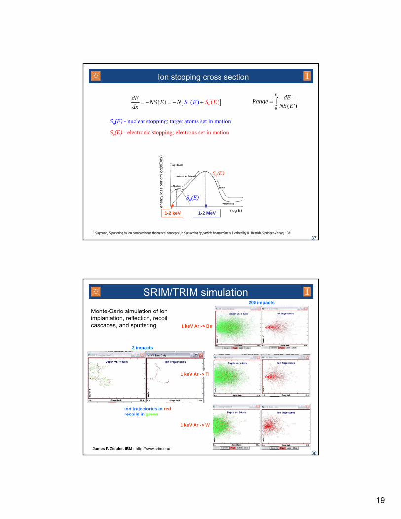
Ion stopping cross section
[ ]( )( )) (en S EdE N N SS E Edx
= − = − +0
'( ')
E dERangeNS E
= ∫
S (E) - nuclear stopping; target atoms set in motion
Se(E)
r cm
log(
dE/d
x)
Sn(E) nuclear stopping; target atoms set in motion
Se(E) - electronic stopping; electrons set in motion
37P.Sigmund, “Sputtering by ion bombardment: theoretical concepts”, in Sputtering by particle bombardment I, edited by R. Behrish, Springer-Verlag, 1981
Sn(E)
1-2 keV
ener
gy lo
ss p
er
1-2 MeV (log E)
SRIM/TRIM simulation
1 keV Ar -> Be
Monte-Carlo simulation of ion implantation, reflection, recoil cascades, and sputtering
200 impacts
1 keV Ar -> Ti
2 impacts
38James F. Ziegler, IBM : http://www.srim.org/
1 keV Ar -> W
ion trajectories in redrecoils in green
20
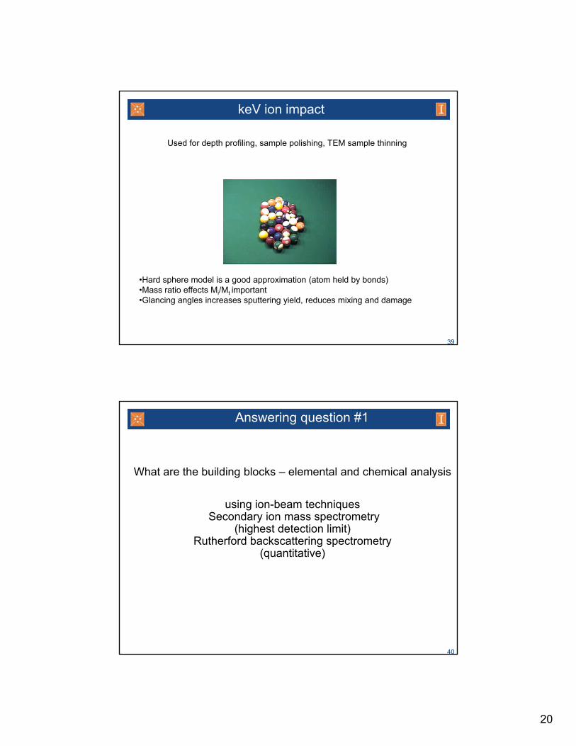
keV ion impact
Used for depth profiling, sample polishing, TEM sample thinning
39
•Hard sphere model is a good approximation (atom held by bonds)•Mass ratio effects Mi/Mt important•Glancing angles increases sputtering yield, reduces mixing and damage
What are the building blocks – elemental and chemical analysis
Answering question #1
using ion-beam techniquesSecondary ion mass spectrometry
(highest detection limit)Rutherford backscattering spectrometry
(quantitative)
40
21
4. What are the surface morphology and bulk nanostructure – imaging from micron to sub-nanometer scale
Answering question #4
g g
usingScanning probe microscopy
Scanning electron microscopy
41
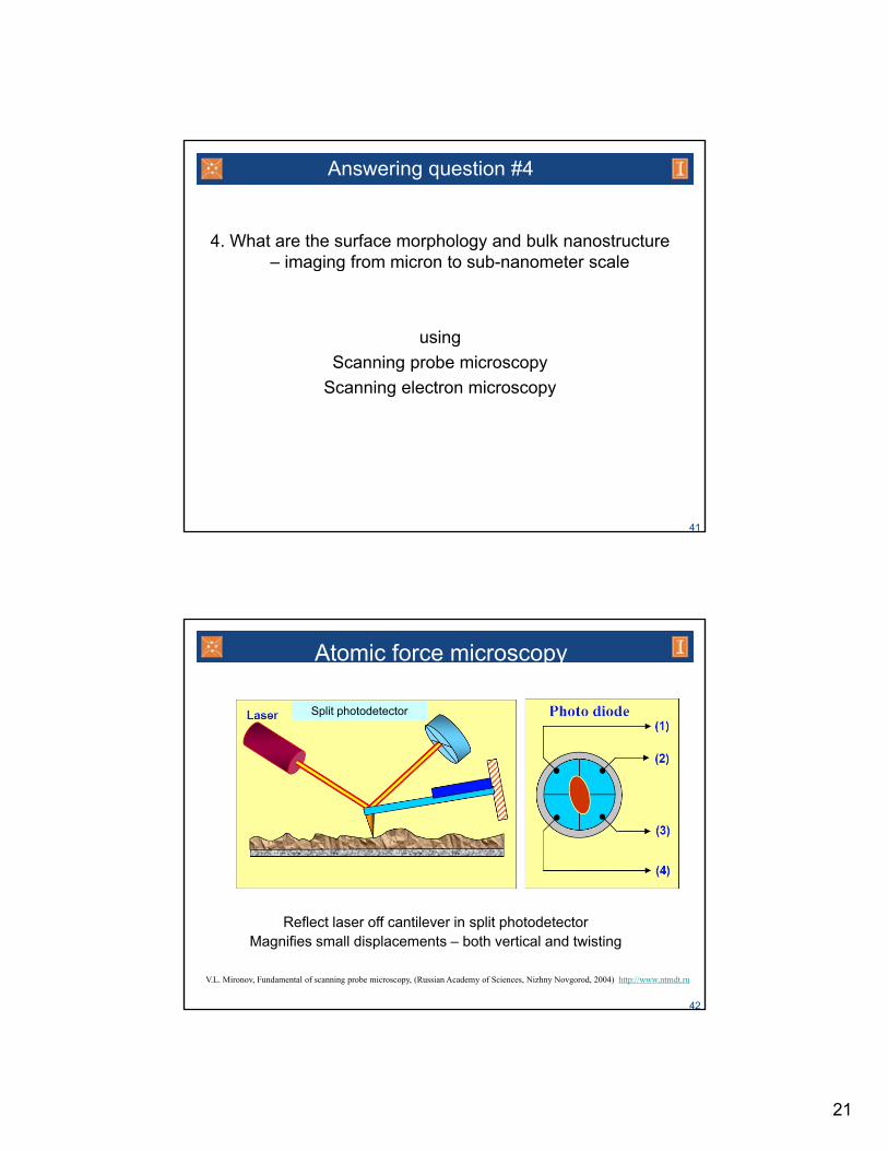
Split photodetector
Atomic force microscopy
42
Reflect laser off cantilever in split photodetectorMagnifies small displacements – both vertical and twisting
V.L. Mironov, Fundamental of scanning probe microscopy, (Russian Academy of Sciences, Nizhny Novgorod, 2004) http://www.ntmdt.ru
22
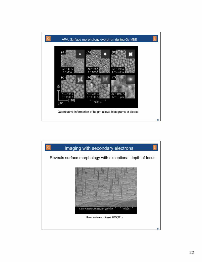
AFM: Surface morphology evolution during Ge MBE
43
Quantitative information of height allows histograms of slopes
Reveals surface morphology with exceptional depth of focus
Imaging with secondary electrons
44
Reactive ion etching of Al/Si(001)
23
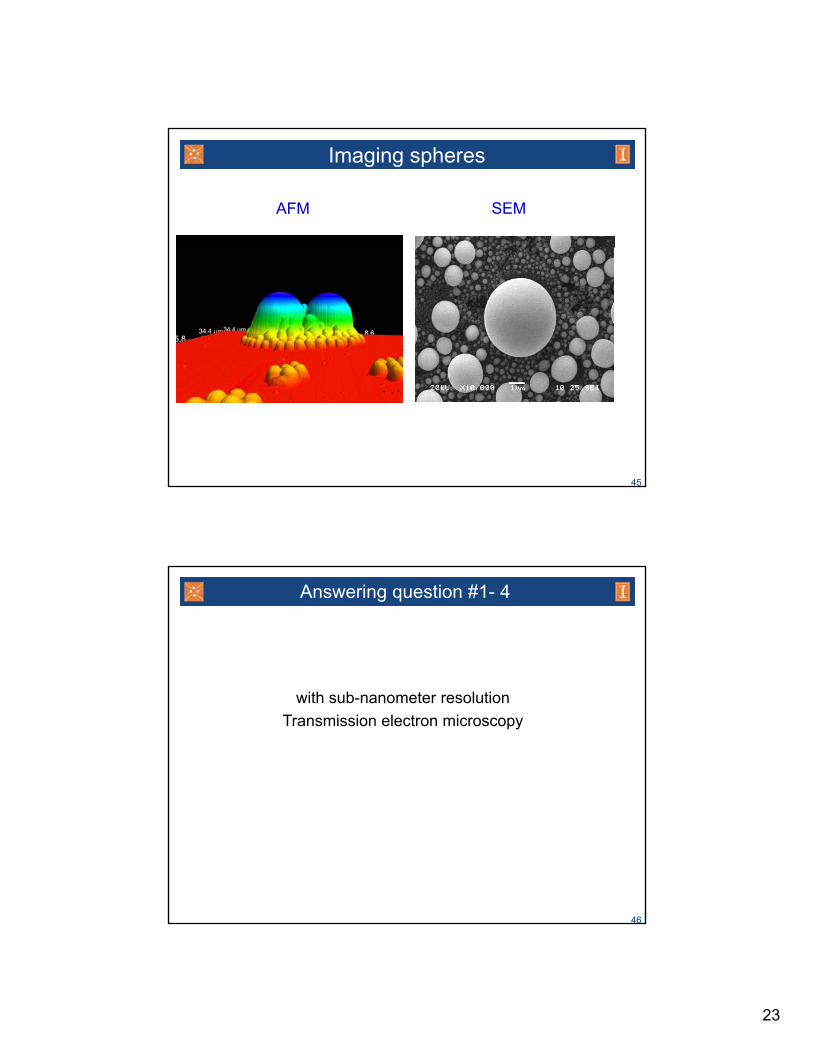
Imaging spheres
AFM SEM
45
Answering question #1- 4
with sub-nanometer resolutionTransmission electron microscopy
46
24
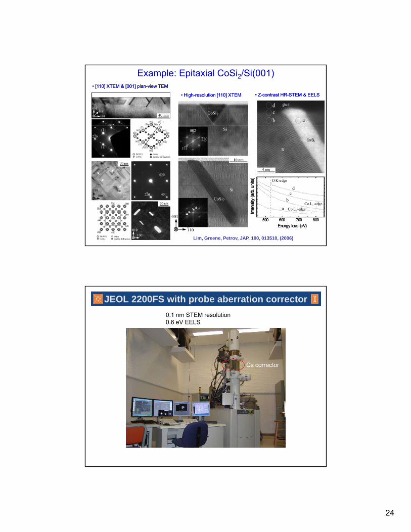
•• HighHigh--resolution [110] XTEMresolution [110] XTEM
Example: Epitaxial CoSi2/Si(001)•• [110] XTEM & [001] plan[110] XTEM & [001] plan--view TEMview TEM
bcd
a
glue
•• ZZ--contrast HRcontrast HR--STEM & EELSSTEM & EELS
nits
)
nits
)
5 nm
CoSi 2
Si
O K-edge
500 600 700 800
Inte
nsity
(arb
. u
Energy loss (eV)
500 600 700 800
Inte
nsity
(arb
. u
Energy loss (eV)
a
bc
d
Co L -edge2
Co L -edge3
Lim, Greene, Petrov, JAP, 100, 013510, (2006)
JEOL 2200FS with probe aberration corrector0.1 nm STEM resolution 0.6 eV EELS
Cs corrector

25
Materials characterization: the need for complementary techniques
Typical sequence to study a set of samples:
1/ non-destructive analysis with no sample preparation to map out phase composition (XRD), surface morphology (AFM, SEM), elemental composition (RBS, EDS)2/ measure physical properties - electrical, mechanical, optical etc.3/ analysis selected samples by surface analysis (e.g. AES, XPS) depth profiling,cross-sectional SEM4/ Select key samples for plan-view and cross-section TEM to understand critical behavior physical properties
49
Examples: synthesis of Ta-N films
Rich phase system.Ta-N phase Structure Lattice constants (Å)
α-Ta cubic a = 3.3058β-Ta tetragonal a = 10.194, c = 5.313
β-TaN0 04 cubic a =10.09
0 5 10
30003020°C
3500
Weight Percent Nitrogen
L
β TaN0.04 cubic a 10.09TaN0.1 cubic a = 3.369Ta4N orthorhombic a = 5.16, b = 3.11, c = 4.94
γ-Ta2N hexagonal a = 3.0445, c = 4.9141TaN0.8 hexagonal a = 2.931, c = 2.879δ-TaN cubic a = 4.33ε-TaN hexagonal a = 5.1918(3), c = 2.9081(2)Ta5N6 hexagonal a = 5.176(6), c = 10.35(3)Ta4N5 tetragonal a = 6.83(13), c= 4.269(6)Ta3N5 orthorhombic a = 3.893, b = c = 10.264
0 10 20 30 40 50 601000
1500
2000
2500
Atomic Percent Nitrogen
Tem
pera
ture
°C
(Ta) γ-Ta N2
ε-TaN
δ-TaN
50
δ-TaN thin films (NaCl-structure) for replacing TiN.- Hard and wear resistant coatings: high hardness and mechanical strength.- Diffusion barrier layers: chemical inertness and low resistivity.
Growth of δ-TaN thin films: reactive magnetron sputtering.

26
)
Ts = 100 °Ct = 500 nm cubic TaN0.1
hexagonal γ-Ta2Ncubic δ-TaNbct-TaNx
+
*TaNx/SiO2/Si(001)GA-XRD 2θ scans TEM
111112321220
fcc bct
Phase identification
Inte
nsity
(a.u
.)
0.063
0.125
0.150
0.250
(311
)
(220
)
*
*
*(2
00)
fN2 = 1
(301
)
(200
)
(110
)
(111
)
110
200
111
200 002301400
51
20 30 40 50 60 70 80
++0.013 (211
)
(200
)
(110
)
2θ (deg)
+
(101
)
0.025 (002
)
(112
)
(110
)
0.050 δ-TaNx: ao = 0.443 nmbct-TaNx: a = 0.590 nm, c = 0.443 nm
N/Ta = 1.96
Growth phase map for TaNx
Pure Ar: tetragonal β-Ta @ Ts < 150 °Cbcc α-Ta @ Ts > 400 °C.
1000= α-Ta= α-Ta + β-Ta
= δ-TaN + ε-TaN= δ-TaN
= Ta4N+TaN0.1
= Ta4N
TaNx growth phase map
Composition measured by RBS and AES
fN2 < 0.1: three consecutive narrow lower nitride regions, defined by tilted boundaries toward higher fN2 with increasing Ts.
0.1 <fN2 < 0.3 and Ts ≤ 650 °C: single-phase δ-TaNx.
400
600
800
1000 β= β-Ta = TaN0.1
= δ-TaN + bct TaN4
= γ-Ta2N = γ-Ta2N + δ-TaN
T s (°C
)
52
0.1 <fN2 < 0.3 and Ts > 650 °C:hexagonal ε-TaNx + δ-TaNx.
Pure N2: δ-TaNx + bct-TaNx.
0 0.1 0.2 0.3 1.00
200
400
fN2
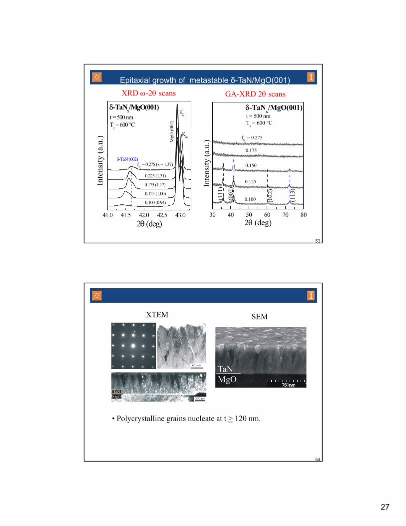
27
t = 500 nmT = 600 °C
δ-TaNx/MgO(001)K
α1
2)
t = 500 nmT 600 °C
δ-TaNx/MgO(001)
XRD ω-2θ scans GA-XRD 2θ scans
Epitaxial growth of metastable δ-TaN/MgO(001)
nten
sity
(a.u
.)
0.125
0.150
fN2
= 0.275
0.175
Ts 600 C
0 175 (1 17)
0.225 (1.31)
fN2
= 0.275 (x = 1.37)
Inte
nsity
(a.u
.)
δ-TaN (002)
Kα2
MgO
(002Ts = 600 °C
53
30 40 50 60 70 80
(113
)
(022
)
(002
)
(111
)
0.100In
2θ (deg)
0.125 (1.00)
0.175 (1.17)I
41.0 41.5 42.0 42.5 43.02θ (deg)
0.100 (0.94)
XTEM SEM
MgOTaN80 nm
300 nm
54
• Polycrystalline grains nucleate at t > 120 nm.
28
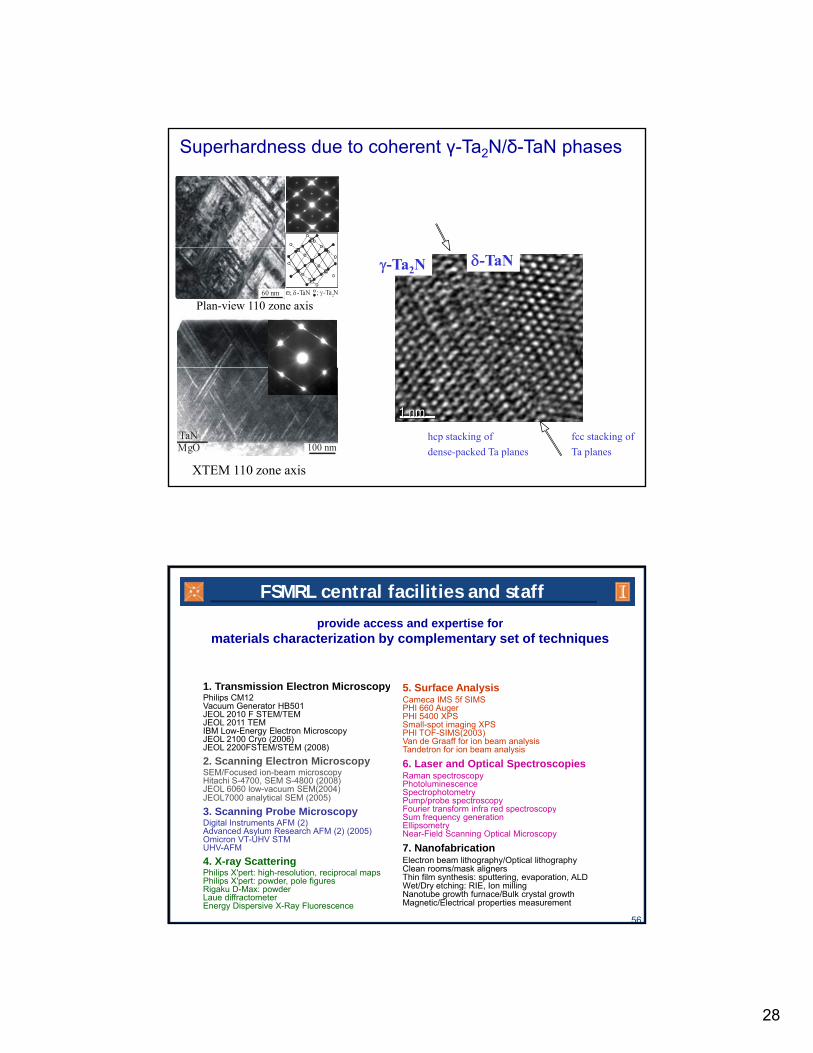
Superhardness due to coherent γ-Ta2N/δ-TaN phases
; -Ta Nγ 2; δ-TaN60 nm
Plan-view 110 zone axis
δ-TaNγ-Ta2N
100 nmMgOTaN
XTEM 110 zone axis
1 nm1 nm
fcc stacking ofTa planes
hcp stacking ofdense-packed Ta planes
FSMRL central facilities and staff
provide access and expertise for materials characterization by complementary set of techniques
1 Transmission Electron Microscopy 5 S f A l i1. Transmission Electron MicroscopyPhilips CM12Vacuum Generator HB501JEOL 2010 F STEM/TEMJEOL 2011 TEMIBM Low-Energy Electron MicroscopyJEOL 2100 Cryo (2006)JEOL 2200FSTEM/STEM (2008)2. Scanning Electron MicroscopySEM/Focused ion-beam microscopyHitachi S-4700, SEM S-4800 (2008)JEOL 6060 low-vacuum SEM(2004)JEOL7000 analytical SEM (2005)
5. Surface AnalysisCameca IMS 5f SIMSPHI 660 AugerPHI 5400 XPSSmall-spot imaging XPSPHI TOF-SIMS(2003)Van de Graaff for ion beam analysisTandetron for ion beam analysis
6. Laser and Optical SpectroscopiesRaman spectroscopyPhotoluminescenceSpectrophotometryPump/probe spectroscopy
56
3. Scanning Probe MicroscopyDigital Instruments AFM (2) Advanced Asylum Research AFM (2) (2005)Omicron VT-UHV STMUHV-AFM4. X-ray ScatteringPhilips X'pert: high-resolution, reciprocal maps Philips X'pert: powder, pole figuresRigaku D-Max: powderLaue diffractometerEnergy Dispersive X-Ray Fluorescence
p p p pyFourier transform infra red spectroscopySum frequency generation EllipsometryNear-Field Scanning Optical Microscopy
7. NanofabricationElectron beam lithography/Optical lithographyClean rooms/mask alignersThin film synthesis: sputtering, evaporation, ALDWet/Dry etching: RIE, Ion millingNanotube growth furnace/Bulk crystal growthMagnetic/Electrical properties measurement