2007 IEEE INTERNATIONAL CIRCUITS
119
ADVANCE PROGRAM 2007 IEEE INTERNATIONAL SOLID-STATE CIRCUITS CONFERENCE FEBRUARY 11,12,13,14,15 CONFERENCE THEME: The 4 Dimensions of IC Innovation SAN FRANCISCO MARRIOTT HOTEL IEEE SOLID-STATE CIRCUITS SOCIETY/IEEE SAN FRANCISCO SECTION, BAY AREA COUNCIL/UNIV. OF PA. SUNDAY ALL-DAY: 3 FORUMS: NV MEMORY; 3D-CHIPSTACKS; PAS AND TXS 10 TUTORIALS 2 SPECIAL-TOPIC SESSIONS: DIGITALLY-ENHANCED ANALOG/RF; CIRCUITS IN 2012 5-DAY PROGRAM THURSDAY ALL-DAY: 4 FORUMS: NOISE IN IMAGERS; AUTOMOTIVE BUSES; DYNAMIC µP OPTIMIZATION; LV AMPS FOR FILTERING/CONVERSION SHORT-COURSE: ANALOG/RF IN nm CMOS
Transcript of 2007 IEEE INTERNATIONAL CIRCUITS

ADVANCE PROGRAM
2007IEEE
INTERNATIONALSOLID-STATE
CIRCUITSCONFERENCE
FEBRUARY11,12,13,14,15
CONFERENCE THEME:
The 4 Dimensions of IC Innovation
SAN FRANCISCOMARRIOTT HOTELIE
EE
SO
LID
-STA
TE C
IRC
UIT
S S
OC
IETY
/IEE
E S
AN
FR
AN
CIS
CO
SE
CTI
ON
, BA
Y A
RE
A C
OU
NC
IL/U
NIV
. OF
PA
.
SUND
AY A
LL-D
AY: 3
FORU
MS:
NV M
EMOR
Y; 3D
-CHI
PSTA
CKS;
PAS
AND
TXS
10 TU
TORI
ALS
2 SPE
CIAL
-TOP
IC SE
SSIO
NS:D
IGITA
LLY-E
NHAN
CED
ANAL
OG/R
F; CIR
CUITS
IN20
12
5-DA
YPR
OGRA
M
THUR
SDAY
ALL
-DAY
: 4 F
ORUM
S:NO
ISE
INIM
AGER
S; AU
TOM
OTIV
EBU
SES;
D YNA
MIC
µP O
PTIM
IZATI
ON; L
V AM
PSFO
RFIL
TERI
NG/C
ONVE
RSIO
N
SHOR
T-CO
URSE
:ANA
LOG/R
F IN
nmCM
OS

ISSCC VISION STATEMENT The International Solid-State Circuits Conference is the foremost global forum for presentation of advances in solid-state circuits and systems-on-a-chip. The Conference offers a unique opportunity for engineers working at the cutting edge of IC design and application to maintain technical currency and to network with leading experts.
CONFERENCE HIGHLIGHTS
On Sunday, February 11, the day before the official opening of the Conference, ISSCC 2007 offers:
A choice of up to 4 of a total of 10 Tutorials Three ISSCC Advanced Circuits Forums: o GIRAFE (GHz Radio Front Ends): Power Amplifiers o Memory: Non-Volatile Memory o Technology Directions: 3-D Electronics
The 90-minute tutorials offer background information and a review of the basics in specific circuit design topics. In the all-day Advanced Circuit Design Forums, leading experts present state-of-the-art design strategies in a workshop-like format. The Forums are targeted at designers experienced in the technical field. On Sunday evening, two Special-Topic Evening Sessions addressing next-generation circuit-design challenges will be offered starting at 7:30PM:
Digitally Enhanced Analog and RF Circuit Design in the Year 2012
The Special-Topic Evening Sessions are open to all ISSCC attendees. On Monday, February 12, ISSCC 2007 offers three plenary papers followed by six parallel technical sessions. A Social Hour open to all ISSCC attendees will follow the afternoon session. The Social Hour will feature posters from the winners of the 2007 joint DAC – ISSCC student design contest and the 2006 Asia Solid-State Circuits Conference student design contest. Monday evening features a panel discussion “Ultimate Limits of Integrated Electronics” and two Special-Topic Evening Sessions:
Last Mile Access Options: PON/DSL/Cable/Wireless Automotive Signal Processing Technologies
On Tuesday, February 13, ISSCC 2007 offers morning and afternoon technical sessions, followed by a Social Hour, an evening panel; “Digital RF - Fundamentally a New Technology or Just Marketing Hype” and three Special-Topic Evening Sessions:
Highlights of IEDM Secure Digital Systems Implantable and Prosthetic Devices
Wednesday, February 14 features morning and afternoon technical sessions. On Thursday, February 15, ISSCC 2007 offers a choice of four events:
An ISSCC Short Course: “Analog, Mixed-Signal and RF Circuit Design in Nanometer CMOS”. Two sessions of the Short Course will be offered, with staggered starting times. Four ISSCC Advanced Circuits Forums: o Microprocessors: Adaptive Techniques for Dynamic
Processor Optimization o Circuit Design: Low-Voltage Analog Amplifier Design for Filtering
and A/D Conversion o ATAC: Automotive Bus Systems o Imager: Noise in Imaging Systems
Registration for educational events will be filled on a first-come, first-served basis. Use of the ISSCC web-registration site (www.isscc.org) is strongly encouraged. You will be provided with immediate confirmation on registration for Tutorials, Advanced Circuit Design Forums and the Short Course.
2

CONTENTS
3
Tutorials ............................................................................................................................................ 4-9 FORUMS
F1 Memory Design Forum.................................................................................................... 10-11 F2 Circuit Design Forum....................................................................................................... 12-13 F3 GIRAFE Design Forum..................................................................................................... 14-15
SPECIAL-TOPIC SESSIONS SE1 Digitally-Enhanced Analog & RF ............................................................................................16 SE2 Circuit Design in the Year 2012 .............................................................................................17
PAPER SESSIONS 1 Plenary Session............................................................................................................... 18-19 2 Optical Communications.................................................................................................. 20-21 3 Emerging Devices and Circuits ........................................................................................ 22-23 4 RF Building Blocks........................................................................................................... 24-25 5 Microprocessors ............................................................................................................. 26-27 6 UWB & mm-Wave Communications ............................................................................... 28-29 7 Display Electronics .......................................................................................................... 30-31
DISCUSSION SESSIONS SE3 Last Mile Access Options: PON/DSL/Cable/Wireless ....................................................... 32-33 E1 Ultimate Limits of Integrated Electronics...............................................................................34 SE4 Automotive Signal Processing Technologies.........................................................................35
PAPER SESSIONS 8 Biomedical Devices.......................................................................................................... 36-37 9 Clocking........................................................................................................................... 38-39 10 mm-Wave Transceivers and Building Blocks................................................................... 40-41 11 TV Tuner/RFID................................................................................................................. 42-43 12 Gigabit CDRs and Equalizers ........................................................................................... 44-45 13 ∆∑ ADCs and Converter Techniques ................................................................................ 46-47 14 Baseband Signal Processing ........................................................................................... 48-49 15 Multimedia and Parallel Signal Processors...................................................................... 50-51 16 Power Distribution and Management .............................................................................. 52-53 17 Analog Techniques & PLLs.............................................................................................. 54-55 18 SRAM .............................................................................................................................. 56-57 19 Cellular and Multi-Mode Transceivers ............................................................................. 58-59 Conference Timetable ............................................................................................................... 60-61 Conference Registration and Hotel-Reservations Forms .................................................... Inserts
PAPER SESSIONS 20 Proximity Data and Power Transmissions....................................................................... 62-63
DISCUSSION SESSIONS SE5 Highlights of IEDM 2006 .......................................................................................................64 SE6 Secure Digital Systems..........................................................................................................65 E2 Digital RF – Fundamentally a New Technology or Just Marketing Hype?............................................................................................................66 SE7 Implantable and Prosthetic Devices: Life-Changing Circuits..................................................67
PAPER SESSIONS 21 Sensors and MEMS ......................................................................................................... 68-69 22 Digital Circuit Innovations ............................................................................................... 70-71 23 Broadband RF and Radar................................................................................................. 72-73 24 Multi-GB/s Transceivers .................................................................................................. 74-75 25 Nyquist ADC Techniques ................................................................................................. 76-77 26 Non-Volatile Memories .................................................................................................... 78-79 27 DRAM and eRAM............................................................................................................. 80-81 28 Image Sensors ................................................................................................................ 82-83 29 Analog & Power Management Techniques ...................................................................... 84-85 30 Building Blocks for High-Speed Transceivers.................................................................. 86-87 31 WLAN/Bluetooth.............................................................................................................. 88-89 32 Trends in Wireless Systems ............................................................................................ 90-91
SHORT COURSE Analog, Mixed-Signal, and RF Circuit Design in Nanometer CMOS............................................... 92-95
FORUMS F4 Imager Design Forum...................................................................................................... 96-97 F5 ATAC ............................................................................................................................... 98-99 F6 Microprocessor Forum................................................................................................ 100-101 F7 Circuit Design Forum................................................................................................... 102-103 Information.............................................................................................................................. 104-108 Committees ............................................................................................................................. 109-115 Conference Information.................................................................................................................116 Hotel Layout ............................................................................................................................ 117-118

TUTORIALS
4
T1: Embedded Power-Management Circuits
Due to the drastic increase of system integration and power consumption of an IC with technology scaling, power management becomes a critical issue in determining the overall performance of the IC. This tutorial starts with a brief overview of power management circuits for embedded applications. There follows a detailed explanation of the operation and design issues associated with various on-chip power converter circuits including linear regulator, switched-inductor regulator, and switched-capacitor regulator. The focus is on the analog circuit techniques, and the control mechanism for implementing these power converters. Instructor: Philip K.T. Mok received his B.A.Sc., M.A.Sc., and Ph.D. degrees in electrical and computer engineering from the University of Toronto, Toronto, ON, Canada, in 1986, 1989, and 1995, respectively. In January 1995, he joined the Department of Electronic and Computer Engineering at the Hong Kong University of Science and Technology, Hong Kong, China, where he is currently an Associate Professor. His current research interests include power-management integrated circuits and low-voltage analog integrated-circuits. He received the Henry G. Acres Medal, the W.S. Wilson Medal, and a Teaching-Assistant Award from the University of Toronto, and the Teaching Excellence Appreciation Award twice from The Hong Kong University of Science and Technology. He has served on the ISSCC analog sub-committee since 2005 and is an associate editor for the IEEE Transactions on Circuits and Systems II and the Journal of Solid-State Circuits since 2006. T2: Continuous-Time ∆Σ Data Converters
While technologies are continuing to provide us with ever faster transistors they also demand that we work at lower supply voltages. The analog designer has to search for new concepts to counteract the reduction of signal swings and increase in power. Although time-continuous circuits are anything but new, they are gaining a renewed interest not only in the academic, but also in the industrial community. With the main focus on baseband applications, different aspects of continuous-time ∆Σ modulators will be covered when operated under low-power and low-voltage constraints:
• Architectures for baseband applications • Implicit anti-aliasing filter • Influence of non-idealities and correction techniques • Implementations (low power, ultra wideband, high performance)
Instructor: Yiannos Manoli holds the Chair of Microelectronics at the University of Freiburg, Germany. His current research interests lie in the design of low-voltage and low-power mixed-signal CMOS circuits, sensor read-out circuits as well as A/D- and D/A-converters with over 150 papers in these areas. He holds a B.A. degree in Physics and Mathematics, a M.S. degree in electrical engineering and computer science from the University of California, Berkeley, and the Dr. Ing. Degree in electrical engineering from the Gerhard Mercator University in Duisburg, Germany.

Sunday, February 11th
5
T3: Dealing with Issues in VLSI Interconnect Scaling
Designers have recognized for many years that on-chip wires can limit system performance, and as technologies continue to scale, the problems posed by on-chip wires continue to worsen. This tutorial introduces models for the resistance, capacitance, and inductance of on-chip wiring and discusses metrics for the delay, bandwidth, noise performance, and energy costs of wires. We consider scaling trends several generations into the future, and how wires perform relative to transistors. We will also examine broader implications of wires for design and CAD tools, notably how they impact architectural trends for both custom and ASIC design flows. Finally, a number of promising design techniques and technologies that can improve the performance of on-chip communication are discussed. Instructor: Ron Ho is a Senior Research Scientist at Sun Microsystems Laboratories in Menlo Park, CA, where he worries about the future of wires. He received his Ph.D. in electrical engineering from Stanford University. From 1993 to 2003, he was at Intel in Santa Clara, CA, where he worked on processors ranging from the 80486 to the 3rd-generation Itanium. In 2003, he joined Sun Labs, where he is currently researching high-performance and low-energy communication technologies, both on a single chip and between two chips. In 2005, he was also a Lecturer at Stanford University, where he taught a graduate class on circuit design. T4: Dynamic Offset-Cancellation Techniques in CMOS
In analog CMOS design, offset is a fact of life! Even in modern processes, device mismatch typically results in offset voltages of several millivolts. But many analog circuits, e.g. precision amplifiers, sensor interfaces, and ADCs require much lower offset levels. Fortunately, by using dynamic offset-cancellation techniques such as auto-zeroing and chopping, microvolt levels of offset can be routinely achieved in standard CMOS. Compared to the alternatives, i.e. the use of huge devices or trimming, the use of dynamic offset-cancellation techniques has the added advantage of also reducing 1/f noise and drift, thus making it possible to design circuits that are thermal-noise limited. In this tutorial, an introduction to the basic theory behind auto-zeroing and chopping will be given, the pros and cons of both techniques highlighted, and recent advances in the state-of-the-art reviewed. Examples will be given of the use of auto-zeroing and chopping in CMOS circuits and systems with residual offsets as low as 50nV. Instructor: Kofi A. A. Makinwa is an Associate Professor at Delft University of Technology, The Netherlands. He received the B.Sc. and M.Sc. degrees from Obafemi Awolowo University, Nigeria, in 1985 and 1988, respectively. In 1989, he received the M.E.E. degree from the Philips International Institute, The Netherlands, and then joined Philips Research Laboratories as a research scientist. In 2004, he received the Ph.D. degree from Delft University of Technology. He holds nine U.S. patents, has (co)-authored over 40 technical papers, and has given tutorials at the Eurosensors and the IEEE Sensors conferences. His main research interests are in the design of precision analog circuitry, ∆Σ modulators, and sensor interfaces. Dr. Makinwa has served on the technical program committees of the ISSCC, the International Solid-State Sensors and Actuators Conference (Transducers), and the IEEE Sensors conference. In 2005, he received the Veni and Simon Stevin Gezel awards from the Dutch Technology Foundation (STW), and was a co-recipient of the ISSCC 2005 Jack Kilby award.

TUTORIALS
6
T5: Error-Correcting Codes for Memories
Today's memories are increasingly susceptible to cosmic-ray-induced errors. In addition, lowering the supply voltage can increase circuit errors by reducing noise margin. Error-correcting code (ECC) can help solve both these problems by adding redundancy that allows recovery from errors. This tutorial starts from the basics of Shannon's theorem, and explores the need of ECC in nano-scale CMOS, soft errors in memory and basic coding such as Hamming code, cyclic code, and BCH code. It covers these topics in the context of modern memory, and their effect in advancing memory performance. The techniques are also applicable to high-speed logic. Instructor: Takayuki Kawahara is a chief researcher at Central Research Laboratory, Hitachi Ltd. Since joining the laboratory in 1985, he has made fundamental contributions in many areas in the field of low-power memories, including subthreshold-current reduction by gate-source self-reverse biasing, an over-drive sense-amplifier scheme, and charge-recycling. Currently, his responsibility is to explore a new conceptual memory. He received B.S. and M.S. degrees in physics in 1983 and 1985, and a Ph.D. degree in electronics in 1993 from Kyushu University, Fukuoka, Japan. T6: CMOS Front-End Circuit Design
In this turorial a general introduction covering system aspects of RF communication and relevant definitions, will be given. The tutorial covers CMOS RFIC design of low noise amplifiers LNAs and downconversion mixers. The circuit-design lecture first treats the modeling of CMOS devices including noise sources. Next, LNA and mixer design is presented from specifications to detailed topology discussions including all relevant aspects like impedance matching, noise figure, gain, bandwidth, linearity, and low-voltage design, without forgetting the crucial and critical RF ESD protection of LNAs. The circuits are illustrated through many measured test chip case studies aiming at RF standards from 1 to 20GHz. Instructor: Marc Tiebout (S'90-M'93) received his M.S. degree in electrical and mechanical engineering in 1992 from the Katholieke Universiteit Leuven (Belgium) and the Ph.D. degree in electrical engineering from the Technical University of Berlin in 2004. In 1993, he joined Siemens, Corporate Research and Development, Microelectronics, in Munich, Germany, designing analog integrated circuits in CMOS and BiCMOS technologies. In 1997 he started the design of RF devices and building blocks in sub-µm CMOS technologies. From 1999 to 2005, he was with Infineon Technologies AG, Munich, Germany, where he worked on RF CMOS circuits and transceivers for cellular wireless communication products and conducted high-frequency RF CMOS research for 17 and 24GHz applications. Since March 2006, he is with Infineon Technologies Austria, Villach, acting as concept engineer for UWB front-end development. His main interest focusses on low-power high-frequency circuits and systems in CMOS. Marc Tiebout serves as a member of the technical program committee of ISSCC and ESSCIRC. He has authored and coauthored more than 30 IEEE publications.

Sunday, February 11th
7
T7: Vector Processing as an Enabler for Software-Defined Radio in Handsets
Wireless radio standards (for cellular, broadcast, connectivity, and positioning) are rapidly proliferating and continuously evolving. Accordingly, the trend in mobile handsets is toward multi-standard and multi-channel solutions (short term), and software defined radio (SDR) and cognitive radio (long term). The required baseband signal processing involves many giga operations per second, at a power budget of only a few hundred mW. In this tutorial we analyze the trade-off between the required flexibility (programmability) versus power consumption and die area for SDR. For a large class of baseband functions (including demodulation, channel estimation, equalization, interference cancellation, synchronization), programmable vector processing (SIMD) is presented as a key enabler for SDR. A number of vector processors are reviewed, ranging from products today to academic prototypes. Instructor: Kees van Berkel is a Fellow at NXP Research in Eindhoven, the Netherlands. He received an M.S. degree (cum laude) in electrical engineering at the Delft University of Technology in 1980 and a PhD degree in computer science from the Eindhoven University of Technology (TU/e, 1992). Since 1996, he is a visiting Professor at the TU/e. During the 90s, he pioneered research on asynchronous VLSI circuits and contributed to their industrial application. Since the late 90s, his research focus moved to architectures for mobile wireless terminals. He initiated and co-architected the EVP, NXP's vector processor for modem applications. His current research interests include software-defined radio, signal processing algorithms, low-power vector DSPs, and interconnect-centric device architectures. T8: Organic-Transistor Circuit Design
Organic transistors are expected to provide a way to build printable, flexible, and large-area electronic systems, which may open up new applications. This tutorial provides a comprehensive view of integrated circuit design approaches based on organic transistors. The tutorial covers organic IC examples like E-skin, sheet-type scanner, and Braille display.
• Technology aspect (process, structure, material, and encapsulation) • Advantages and disadvantages • Circuit design (modeling, and what are the differences from silicon) • Coping with issues of low speed and reliability • Applications and design examples • Remaining issues and future directions
Instructor Takayasu Sakurai received the B.S., M.S. and Ph.D degrees in electrical engineering from University of Tokyo. In 1981, he joined Toshiba, where he designed numerous VLSI products including memories and processors. From 1988 to 1990, he was a visiting researcher at University of California, Berkeley. From 1996, he is a Professor at University of Tokyo, working on VLSI design and organic circuits. He was a conference chair and a TPC member of international conferences in the field of VLSI design including ISSCC, VLSI Circuit Symp., A-SSCC, CICC, ESSCIRC, and DAC. He is a recepient of 2005 IEEE ICICDT award, 2004 IEEE Takuo Sugano award, 2005 P&I patent of the year award, and other awards. He is an IEEE Fellow, a STARC Fellow, an elected AdCom member for the IEEE SSCS, and an IEEE CAS and SSCS distinguished lecturer.

TUTORIALS
8
T9: Radio Design for MIMO Systems with an Emphasis on IEEE 802.11n
Essential to the overall system design of a MIMO system, is the radio design. This course will provide a brief introduction to the legacy 802.11 a/b/g systems, followed by a discussion of the history of multiple antenna systems and the conventional analog-based techniques such as MRC. A general introduction to the 802.11n will then follow, which includes the channelization and modulation types, the definition and the description of the concepts behind the multiple spatial streams (MxN), and additional PHY and MAC techniques allowing for higher rates and/or longer reach. These features include the use of short guard-interval (GI), implicit and explicit beam-forming, space-time block codes (STBC), the use of Greenfield mode, and aggregation techniques. The requirements of 802.11n standard such as sensitivity and EVM and their relation to analog impairments such as phase noise, quadrature imbalances, linearity, and cross-talk will also be discussed. Some specific circuit examples will be presented and some unique circuit implementation challenges of MIMO radios will be discussed. Some measured performance numbers (range and throughput) will be also presented. The course will wrap up by discussing the future trends of MIMO radio implementation.
Instructor: Arya Behzad has worked in various senior circuit and system design capacities at various companies. Since 1998 he has been with Broadcom Corporation working on integrated tuners, gigabit Ethernet and wireless LAN systems and ICs. He is currently a Director of Engineering working on radios for current and future generation wireless products, and Product Line Manager for all Wireless LAN Radio products. He has over 70 patents issued and pending as well as many publications in the areas of precision analog circuits, cellular transceivers, integrated tuners, gigabit Ethernet, and wireless LANs. He has taught courses and presented technical seminars at various conferences and at several universities. Mr. Behzad is on his fifth year serving as a member of the ISSCC Wireless Technical Committee. He has served as a Guest Editor of JSSC and is currently an Associate Editor of the Journal. Mr. Behzad obtained his M.S. EE from UC Berkeley in 1994 after completing his thesis on the Infopad project.

Sunday, February 11th
9
T10: Fundamentals of Electronic Dispersion Compensation
Electronic dispersion compensation (EDC) has emerged as the technology enabling the migration of metro and long-haul optical fiber and backplane links to 10Gb/s to 40Gb/s rates. Both links suffer from various forms of dispersion or intersymbol interference (ISI), and noise. Fiber links also exhibit non-linearities due to fiber amplifiers and the photo-detector. The stringent power and throughput requirements have forced transmit and receiver ICs to be predominantly mixed-signal and the modulation to be binary. Meeting the challenges of designing next generation high data rate systems within a tight power budget requires the designer to understand the very basis of information transfer and go beyond the waveform shaping aspect exemplified by the ‘eye-opening’ techniques prevalent today. This tutorial will provide an overview of efficient transmit and receive techniques for both linear (back-plane) and non-linear (fiber) channels such as matched filtering, linear, decision-feedback, transmit techniques (pre-emphasis and partial response coding), maximum likelihood detector (‘Viterbi equalizer’) and their implications on mixed-signal design. The design of an OC-192 EDC chip-set will be presented as a case-study. Finally, the tutorial will conclude with a discussion on advanced topics and future directions. Instructor: Naresh Shanbhag is currently a Professor in the Department of Electrical and Computer Engineering and the Coordinated Science Laboratory at the University of Illinois at Urbana-Champaign, Urbana, IL, USA. His research interests are in the area of low-power/high-performance integrated circuits and systems for DSP and communications. He is also a co-founder and Chief Technology Officer of Intersymbol Communications, Inc., (a wholly owned subsidiary of Kodeos Communications, Inc., since March 2006) Champaign, IL, USA, which was founded in 2000, and where he provides strategic directions in the development of EDC based mixed-signal receivers for next generation optical fiber links. He received his Ph.D. in EE from the University of Minnesota, located in Minneapolis, USA, in 1993. From 1993, Dr. Shanbhag worked at AT&T Bell Laboratories where he lead the development of its 51.84Mb/s VDSL chip-sets before joining the University of Illinois in 1995. Dr. Shanbhag became an IEEE Fellow in 2006, received the 2001 IEEE Transactions on VLSI Best Paper Award, the 1999 IEEE Leon K. Kirchmayer Best Paper Award, the 1999 Xerox Faculty Award, the Distinguished Lecturership from the IEEE Circuits and Systems Society in 1997, the National Science Foundation CAREER Award in 1996, and the 1994 Darlington Best Paper Award from the IEEE Circuits and Systems Society. From 1997 to 1999 and from 1999 to 2002, he served as an Associate Editor for the IEEE Transaction on Circuits and Systems: Part II and the IEEE Transactions on VLSI, respectively.

MEMORY DESIGN FORUM
10
F1: Non-Volatile Memory Circuit Design and Technology
Organizer/Chair: Mark Bauer, Intel, Folsom, CA Committee: Giulio Casagrande, ST Microelectronics, Milano,Italy Hideto Hidaka, Renesas, Itami, Hyogo, Japan Yair Sofer, Saifun Semiconductors, Netanya, Isreal Solid-state non-volatile memories have seen explosive growth in the last few years in electronic applications such as memory cards, cell phones, still and video cameras, digital music, video players and other consumer electronic devices. With the memory cost per bit reducing at very aggressive rates, the industry is seeing even more solid-state non-volatile memory applications emerging such as disk caches and solid-state disks for use in personal and portable computers. Application requirements for low-cost, low-power, high-performance non-volatile memory, and major challenges associated with aggressively scaling process technologies have driven the industry to many new circuit design, architecture and technology innovations.
Floating gate structures continue to dominate non-volatile memory technology. These structures typically use a polysilicon floating gate as the storage node and are arranged in various memory arrays to achieve architectures such as NAND flash and NOR flash memory. To program and erase the memory cell, electron tunneling methods are used to place or remove electrons from the floating gate. Other material types are being developed as floating gate replacements such as NROM memories where the storage material is a nitride material. Non-electron storage non-volatile memory types such as PRAM (phase-change RAM) and MEMS-based memories are also being researched. Alternative cell structures such as FeRAM (ferro-electric RAM) and MRAM (magnetic RAM) have recently become commercially available. These newer memory types have the potential to be used in existing non-volatile memory sockets or drive new applications.
Many circuit design and architectural innovations have been developed over the years to overcome scaling challenges and improve performance on established non-volatile memory technologies. New circuit and architecture development are required to design a memory using the new cell types and structures. Multi-level design, multi-bit design and, on-chip read/write buffer architectures are just a few examples.
The Advanced Circuits Forum on Non-Volatile Memory Circuit Design and Technology will first present an overview of floating-gate type non-volatile memory cells and structures along with recent advancements in extensions of electron storage with new material types. In addition, new memory cell types and structures using different materials will be discussed along with the challenges associated with integration of new materials into a CMOS technology. The discussion of technology will lay the foundation for the subsequent discussions on design techniques for the various non-volatile memory types. Following the design discussions, we will explore different non-volatile memory applications and how the various memory technologies and designs fit within the range of applications.
This all day forum encourages open exchange in a closed forum. Attendance is limited and pre-registration is required. Coffee breaks and lunch will be provided to allow a chance for participants to discuss the issues and ask follow-up questions to the forum presenters.

Sunday, February 11th 8:00 AM
11
Forum Agenda
Time Topic 8:00 Continental Breakfast 8:30 Introduction and Overview Mark Bauer, Intel, Folsom, CA 9:00 Non-Volatile Memory Technology: Present and Future Trends Al Fazio, Intel, Santa Clara, CA 10:15 Break 10:30 NOR Flash Memory Design Kerry Tedrow, Intel, Folsom, CA 11:30 NAND Flash Memory Design Tomoharu Tanaka, Micron, Kamata, Japan 12:30 Lunch 1:15 NROM Memory Design Yair Sofer, Saifun Semiconductors, Netanya, Israel 2:00 Embedded Flash Memory Design Hideto Hidaka, Renesas, Itami, Japan 2:45 Break 3:00 Circuits and Design Challenges for Alternative and Emerging NVM Shine Chung, TSMC, Shin-Chu, Tiawan 4:00 Non-Volatile Memory Applications Koji Sakui, Sony, Japan 5:00 Parting Remarks and Wrap-up

CIRCUIT DESIGN FORUM
12
F2: Design of 3D-Chipstacks Organizer: Werner Weber, Infineon Technologies, Munich, Germany Co-Organizer: William Bowhill, Intel, Hudson, MA Committee: Kerry Bernstein, IBM Yorktown Heights, NY
Anantha Chandrakasan, MIT, Cambridge, MA Ronald Ho, Sun Microsystems, Menlo Park, CA Peter Kogge, University of Notre Dame, Notre Dame, IN Samuel Naffziger, Advanced Micro Devices, Fort Collins, CO Hiroyuki Mizuno, Hitachi, Tokyo, Japan
Many experts claim that ‘Moore’s Law’ will gradually come to its end and will be replaced by new innovations headlined by the term ‘More Than Moore.’ Among others, this term comprises advanced multi-chip integration methods such as 3D System Integration. This technology provides high-potential performance benefits in terms of geometry and speed and has drawn major attention by a large number of research groups in the past few years. Numerous process architectures have been developed and the first cost-effective commercialized applications in the communications and memory fields are expected to come to market soon. The objective of this forum is to introduce the different process architectures and present potential applications to be deployed in the coming years. The forum will provide an overview of the field and the different technological approaches. Digging deeper, it will provide an understanding of potential memory and processor applications giving performance and cost arguments. The forum is intended for circuit and system designers and engineering students wishing to gain insight into this interface between circuit design, system design and packaging and how it may impact applications in the near future. The forum will start with a technology overview by Harry Hedler (Qimonda) highlighting the different process architectures and their benefits and shortcomings. In the second presentation, Mitsumasa Koyanagi (Tohoku U) will present prototypes based on wafer-to-wafer stacking and chip-to-wafer stacking. He became a father of 3D integration when he introduced wafer stacking 25 years ago. Muhannad Bakir (Georgia Tech) will then address the important topics of heat removal and power distribution in the chip-stacks. The technology section is then concluded with a presentation by Tadahiro Kuroda (Keio U) who will address chip-to-chip data communication by inductive and capacitive coupling. The applications section starts with a presentation by Dan Radack (DARPA) who provides an overview of possible applications and their advantages and disadvantages. Wilfried Haensch (IBM) will then discuss the processor applications, elaborating on alternative integration strategies. Bryan Black (Intel) will continue the discussion of processor applications and discuss design challenges of 3D integration. Dong-Ho Lee (Samsung) will contrast this with memory applications. The presentation by Bert Gyselinckx (IMEC) will highlight the opportunities of 3D integration for miniaturized wireless sensor networks. Finally, Hannu Tenhunen (KTH Sweden) will elaborate on the cost and performance trade-offs for 3D mixed signal systems. The forum concludes with a panel discussion, which will provide the audience the chance to engage in extended discussions with the presenters.

Sunday, February 11th 8:00 AM
13
Forum Agenda Time Topic 8:00 Breakfast
8:20 Introduction Werner Weber, Infineon, Munich, Germany
3D Technologies
8:30 Status, Opportunities and Trends of 3D Integration by Thru-Silicon-Via Stacking
Harry Hedler, Qimonda, Munich, Germany
9:15 New Three-Dimensional Integration Technologies Based on Wafer-to-Wafer and Chip-to-Wafer Bonding Methods Mitsumasa Koyanagi, Tohoku University, Sendai, Japan
10:00 Break
10:15 Heat Removal and Power Delivery for 3D SoC Muhannad Bakir, Georgia Institute of Technology, Atlanta, GA
10:45 CMOS Proximity Wireless Communications of SiP Integration Tadahiro Kuroda, Keio University, Yokohama, Japan
3D Applications
11:15 Applications of 3D Integration Dan Radack, DARPA, Arlington, VA
11:45 Is 3D the Next Big Thing in Microprocessors? Wilfried Haensch, IBM, Yorktown Heights, NY
12:15 Lunch
1:15 3D Design Opportunities and Challenges for Microprocessors Bryan Black, Intel, Austin, TX
1:45 3D Chip Stacking Technology for Memory Device Dong-Ho Lee, Samsung, Yongin City, Korea
2:30 Break
2:45 3D System-in-Package Integration of Wireless Sensor Nodes Bert Gyselinckx, IMEC, Leuven, Belgium
3:30 Performance and Cost Trade-Offs for SoC, SoP and 3D Integration Hannu Tenhunen, Royal Institute of Technology, Kista, Sweden
4:00 Panel discussion
5:00 Conclusion

GIRAFE DESIGN FORUM
14
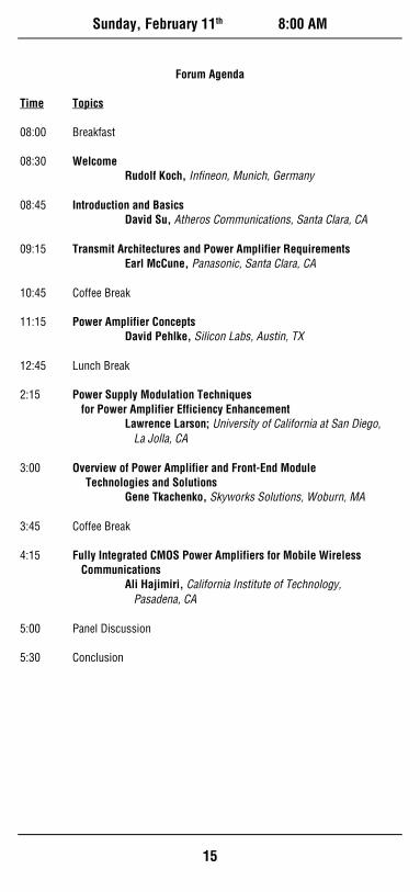
F3: Power Amplifiers and Transmitter Architectures Organizer: Rudolf Koch, Infineon Technologies, Germany
Co-Organizer: Francesco Svelto, University of Pavia, Pavia, Italy
Committee: David Su, Atheros Communications, Santa Clara, CA Tony Montalvo, Analog Devices, Raleigh, NC Ali Hajimiri, California Institute of Technology,
Pasadena, CA Aarno Paerssinen, Nokia, Helsinki, Finland Arya Behzad, Broadcom, San Diego, CA In this all-day forum, new trends in power amplifiers and (PAs) transmit architectures for wireless communications will be discussed.
Mobile phones are evolving from single-standard voice phones to multi-standard multi-band multi-application mobile terminals. High integration levels and re-configurability of the signal processing chain are a must for those all-in-one phones to minimize chip area and cost, but have so far only been demonstrated in transceivers. For entry-level phones single-chip transceiver and baseband integration is a reality now. Power amplifiers, however, have so far been resisting this trend — at least in cellular applications. One PA per band and per standard will be too bulky and too expensive for future terminals. Future PAs must be reconfigurable to support several standards. Silicon integration is a requirement for “intelligent” PAs and is promising cost reduction over III-V PAs, but can it handle the power levels and peak voltages of cellular phones? A variety of PA architectures promises high PAE under certain conditions. For power efficient structures it is, however, no longer sufficient to optimize the PA alone. Rather co-development and common optimization of transmitter, PA, and power supply is required. This forum will highlight the latest trends in PA and transmitter design.
The morning session begins with an introduction into the topic by David Su (Atheros). The second speaker, Earl McCune (Panasonic) will discuss transmit architectures, their impact on the PA concept, and show practical results for various approaches. The third and last speaker of the morning session, David Pehlke (Silicon Labs) will look in detail into a variety of PA concepts and linearization techniques and explain their tradeoffs.
The afternoon session will be opened by Lawrence Larson (UC San Diego), who will show how the various power supply modulation schemes can be used to enhance PA efficiency. Special attention will be given to OFDM applications. The fifth speaker, Gene Tkachenko (Skyworks Solutions) will cover technology requirements and solutions for cellular PAs and front-end modules. The effects of critical system parameters on technology choice will be explained. Finally, Ali Hajimiri (CalTech) will show novel circuit concepts enabling CMOS integration of power amplifiers even for GSM.
The forum will conclude with a panel discussion, where the attendees have the opportunity to ask questions and to share their views.
Attendance is limited and pre-registration is required. This all-day forum encourages open information exchange.
The targeted participants are circuit designers and concept engineers working on wireless transmitters or power amplifiers who want to learn about the latest developments in system and circuit design.
Sunday, February 11th 8:00 AM
15
Forum Agenda
Time Topics 08:00 Breakfast 08:30 Welcome Rudolf Koch, Infineon, Munich, Germany 08:45 Introduction and Basics David Su, Atheros Communications, Santa Clara, CA 09:15 Transmit Architectures and Power Amplifier Requirements Earl McCune, Panasonic, Santa Clara, CA 10:45 Coffee Break 11:15 Power Amplifier Concepts David Pehlke, Silicon Labs, Austin, TX 12:45 Lunch Break 2:15 Power Supply Modulation Techniques
for Power Amplifier Efficiency Enhancement Lawrence Larson; University of California at San Diego, La Jolla, CA
3:00 Overview of Power Amplifier and Front-End Module
Technologies and Solutions Gene Tkachenko, Skyworks Solutions, Woburn, MA 3:45 Coffee Break 4:15 Fully Integrated CMOS Power Amplifiers for Mobile Wireless
Communications Ali Hajimiri, California Institute of Technology, Pasadena, CA
5:00 Panel Discussion 5:30 Conclusion

SPECIAL-TOPIC EVENING SESSIONS
16
SE1: Digitally-Enhanced Analog & RF Co-Organizer: Kari Halonen, Helsinki University of Technology, Espoo, Finland Co-Organizer: Stefan Heinen, Infineon Technologies, Duisburg, Germany Chair: Robert Neff, Agilent, Santa Clara, CA As CMOS chip technologies scale to finer line widths, smaller devices, and lower voltages, the job of the analog circuit designer is getting harder every year. Analog circuit targets are harder to achieve with larger device mismatch, non-ideal device characteristics, and less voltage available for design. At the same time, the scaled technologies reduce power and area for digital circuits, and modern design tools make digital signal processing and control lower cost every year. The trends promise the displacement of high linearity, highly accuracy, challenging analog circuits by lower performance analog, enhanced by digital signal processing. The final achievement is better performance, at lower cost and design time.
Time Topics 7:30 Digitally Assisted Analog Circuits – A Motivational Overview
Boris Murmann, Stanford University, Stanford, CA 8:00 Digitally Corrected Data Converters
Steve Lewis, University of California, Davis, CA 8:30 Digital Calibration and Linearity Correction in RF Transceivers
Larry Larson, University of California, San Diego, CA 9:00 Digitally Controlled Radios: Clean RF Building Blocks for Flexibility
and Energy Efficiency Jan Craninckx, IMEC, Leuven, Belgium

Sunday, February 11th 7:30 PM
17
SE2: Circuit Design in the Year 2012 Co-Organizer: Anantha Chandrakasan, Massachusetts Institute of
Technology, Cambridge, MA Co-Organizer / Chair: Kerry Bernstein, IBM, Yorktown Heights, NY
This special-topic-session will provide a thorough overview of special circuit design considerations which will accommodate sub-32nm device idiosyncrasies. While it is known that scaling effects will continue to profoundly impact high speed logic, designers rarely get a glimpse of the integrated response of all the resources on–board future high performance processors. Four experts will share their insight into issues confronting microprocessor and mixed-signal design in 2012 and offer potential solutions. Time Topics 7:30 Impact of Future Technology Scaling Options on
Processor Design, David Frank, IBM, TJ Watson, Yorktown Heights, NY
8:00 Technology Scaling and Analog Circuits:
Challenges and Solutions, Hae-Seung Lee, Massachusetts Institute of
Technology, Cambridge, MA 8:30 Digital Circuit Design Insights from Analog Experiences,
Marcel Pelgrom, Philips Research, Eindhoven, The Netherlands
9:00 Will FinFETs Replace Planar CMOS by Year 2012?, Borivoje Nikolic, University of California, Berkeley, CA

SESSION 1
18
PLENARY SESSION - INVITED PAPERS Chair: Timothy Tredwell, Eastman Kodak, Rochester, NY
ISSCC Executive-Committee Chair Associate Chair: Jan Van der Spiegel, University of Pennsylvania,
Philadelphia, PA ISSCC Program-Committee Chair
FORMAL OPENING OF THE CONFERENCE 8:30AM 1.1 Foundry Future: Challenges in the 21st Century 8:40 AM
Morris Chang, Taiwan Semiconductor Manufacturing, Hsinchu, Taiwan The dedicated-foundry industry was established in 1987, with the incorporation of Taiwan Semiconductor Manufacturing Company (TSMC). Silicon-wafer production at foundries has increased significantly since that time, to account for over 20% of all wafer volume; Foundries are now an integral part of the overall semiconductor supply-chain. There is every reason to anticipate that the importance of the foundry industry will increase further: We believe that the foundry business-model is an important positive influence on the health of the overall IC industry. Accordingly, it is critically necessary to scan the future for potential issues that might inhibit foundry-industry growth. We see two significant challenges that the foundry industry must address, in order to ensure its continued expansion:
The first and foremost challenge is business growth: We anticipate that growth matching previous industry experience may be more difficult to attain in the future, simply because revenue growth of the semiconductor IC industry (as a whole) has slowed since 2000. Prior to this, the average industry growth-rate was 16%, but, over the period 2000 to 2010, the growth rate will slow to 6%. Additionally, the penetration of the CMOS-logic market by the foundry industry cannot continue unabated indefinitely; saturation should be anticipated in the future. The second challenge for the foundry industry is to maintain profitability: The growth of the industry has attracted many companies to offer foundry services. Consequently, competition between these companies increases the potential for commoditization of foundry services, where many foundries, with apparently similar (but substantively different) services, compete on the basis of price alone. We believe that the foundry industry must respond to these challenges by two means: expanding into new IC-product markets enabled by the cost reduction and performance increases resulting from technology scaling; and by penetrating segments of the IC market that are currently not involved in foundry relationships, by broadening the range of technologies that are offered. In the future, circuit designers can expect, therefore, to be able to access process technologies tuned in various ways: For memory, analog, high-performance-logic, or image-sensor applications, as well as for CMOS logic. The foundry company must develop strategies to avoid commoditization! In our opinion, one of the most important aspects of the foundry response to commoditization must be to create a much deeper and broader relationship between the foundry and each of its customers. This new type of integrated relationship differs from many previous foundry–customer relationships, in that both design and technology engineering proceed concurrently from an early stage in the product-development effort. Note that the success of this relationship will require a much greater information flow between the design and foundry teams, and optimization of both design and process technology to meet product requirements. Such relationships can offer a significant advantage to customers in meeting product-cost, performance, and time-to-market requirements. ISSCC, SSCS, JSSCC, & IEEE AWARD PRESENTATIONS 9:30 AM
BREAK 10:00 AM
Monday, February 12th 8:30 AM
19
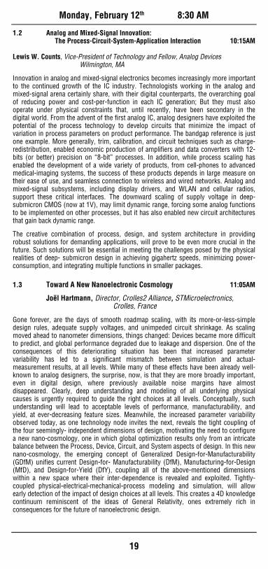
1.2 Analog and Mixed-Signal Innovation: The Process-Circuit-System-Application Interaction 10:15AM
Lewis W. Counts, Vice-President of Technology and Fellow, Analog Devices
Wilmington, MA
Innovation in analog and mixed-signal electronics becomes increasingly more important to the continued growth of the IC industry. Technologists working in the analog and mixed-signal arena certainly share, with their digital counterparts, the overarching goal of reducing power and cost-per-function in each IC generation; But they must also operate under physical constraints that, until recently, have been secondary in the digital world. From the advent of the first analog IC, analog designers have exploited the potential of the process technology to develop circuits that minimize the impact of variation in process parameters on product performance. The bandgap reference is just one example. More generally, trim, calibration, and circuit techniques such as charge-redistribution, enabled economic production of amplifiers and data converters with 12-bits (or better) precision on “8-bit” processes. In addition, while process scaling has enabled the development of a wide variety of products, from cell-phones to advanced medical-imaging systems, the success of these products depends in large measure on their ease of use, and seamless connection to wireless and wired networks. Analog and mixed-signal subsystems, including display drivers, and WLAN and cellular radios, support these critical interfaces. The downward scaling of supply voltage in deep-submicron CMOS (now at 1V), may limit dynamic range, forcing some analog functions to be implemented on other processes, but it has also enabled new circuit architectures that gain back dynamic range.
The creative combination of process, design, and system architecture in providing robust solutions for demanding applications, will prove to be even more crucial in the future. Such solutions will be essential in meeting the challenges posed by the physical realities of deep- submicron design in achieving gigahertz speeds, minimizing power- consumption, and integrating multiple functions in smaller packages.
1.3 Toward A New Nanoelectronic Cosmology 11:05AM
Joël Hartmann, Director, Crolles2 Alliance, STMicroelectronics, Crolles, France
Gone forever, are the days of smooth roadmap scaling, with its more-or-less-simple design rules, adequate supply voltages, and unimpeded circuit shrinkage. As scaling moved ahead to nanometer dimensions, things changed: Devices became more difficult to predict, and global performance degraded due to leakage and dispersion. One of the consequences of this deteriorating situation has been that increased parameter variability has led to a significant mismatch between simulation and actual-measurement results, at all levels. While many of these effects have been already well-known to analog designers, the surprise, now, is that they are more broadly important, even in digital design, where previously available noise margins have almost disappeared. Clearly, deep understanding and modeling of all underlying physical causes is urgently required to guide the right choices at all levels. Conceptually, such understanding will lead to acceptable levels of performance, manufacturability, and yield, at ever-decreasing feature sizes. Meanwhile, the increased parameter variability observed today, as one technology node invites the next, reveals the tight coupling of the four seemingly- independent dimensions of design, motivating the need to configure a new nano-cosmology, one in which global optimization results only from an intricate balance between the Process, Device, Circuit, and System aspects of design. In this new nano-cosmology, the emerging concept of Generalized Design-for-Manufacturability (GDfM) unifies current Design-for- Manufacturability (DfM), Manufacturing-for-Design (MfD), and Design-for-Yield (DfY), coupling all of the above-mentioned dimensions within a new space where their inter-dependence is revealed and exploited. Tightly-coupled physical-electrical-mechanical-process modeling and simulation, will allow early detection of the impact of design choices at all levels. This creates a 4D knowledge continuum reminiscent of the ideas of General Relativity, ones extremely rich in consequences for the future of nanoelectronic design.

SESSION 2
20
OPTICAL COMMUNICATIONS
Chair: Sung Min Park, Ewha Womans University, Seoul, Korea Associate Chair: Yuriy Greshishchev, Nortel, Ottawa, Canada
2.1 A Fully Integrated 4×10Gb/s DWDM Optoelectronic Transceiver in a Standard 0.13µm CMOS SOI
1:30 PM A. Narasimha, B. Analui, Y. Liang, T. Sleboda, C. Gunn Luxtera, Carlsbad, CA
A 4-wavelength DWDM optoelectronic transceiver, implemented in a 0.13μm CMOS SOI process, achieves an aggregate rate of 40Gb/s transmission over single fiber. It integrates four 10Gb/s transceivers consisting of modulator drivers, optical modulators, optical multiplexers and demultiplexers, and TIAs to achieve a BER of <10-12 and a power consumption of 120mW.
2.2 A 90nm CMOS 16Gb/s Transceiver for Optical Interconnects 2:00 PM
S. Palermo1, A. Emami-Neyestanak2, M. Horowitz1 1Stanford University, Stanford, CA, 2Columbia University, New York, NY
An optical interconnect transceiver incorporates a 4-tap FIR TX to reduce VCSEL average current and an integrating/double-sampling RX to eliminate the need for a bit-rate TIA. A dual-loop CDR with baud-rate phase detection further reduces power and area. Fabricated in a 1V 90nm CMOS process, the transceiver achieves 16Gb/s operation while consuming 129mW and occupying 0.105mm2.
2.3 A 20Gb/s Burst-Mode CDR Using Injection-Locking Technique 2:30 PM
J. Lee, M. Liu National Taiwan University, Taipei, Taiwan
The design and experimental verification of a 20Gb/s CDR circuit based on injection-locking technique is presented. Fabricated in 90nm CMOS technology, this circuit achieves a BER of <10-9 for both continuous and burst modes. It has tunability of over 800Mb/s while consuming 175mW. The re-acquisition time of this CDR is 1b interval. Break 3:00 PM
2.4 A 33.6-to-33.8Gb/s Burst-Mode CDR in 90nm CMOS 3:15 PM
L-C. Cho, C. Lee, S-I. Liu National Taiwan University, Taipei, Taiwan
A 33.6-to-33.8Gb/s burst-mode CDR circuit is realized in 90nm CMOS technology. The LC gated VCO, the phase selector, the input matching circuit, and the wideband data buffer are discussed. With 211-1 PRBS input, the measured rms jitter for the recovered data is 1.15ps at 33.72Gb/s. This CDR can tolerate 31 consecutive identical bits with a locking time of 0.2ns(<7b interval). It consumes 73mW from a 1.2V supply excluding the buffers.

Monday, February 12th 1:30 PM
21
2.5 A CMOS Burst-Mode TIA with Step AGC and Selective Internally Created Reset for 1.25Gb/s EPON
3:45 PM Q. Le1, S-G. Lee1, H-Y. Kang2, S-H. Chai3 1Information and Communcations University, Daejeon, Korea 2Electronics and Telecommunications Research Institute, Daejeon, Korea 3Hoseo University, Choongnam, Korea
A selective internal reset mechanism that allows the burst-mode TIA to recover a burst-mode signal as a stand-alone device in EPON is discussed. Using step AGC, the TIA achieves a DR of 27dB and a sensitivity of -31dBm with a PIN photodiode. Moreover, with internal reset, the loud/soft ratio is also 27dB within 100ns guard and preamble times.
2.6 A 40mW 3.5kΩ 3Gb/s CMOS Differential Transimpedance Amplifier Using Negative-Impedance Compensation
4:00 PM C-M. Tsai1, L-R. Huang2 1National Chiao Tung University, Hsinchu, Taiwan 2Industrial Technology Research Institute, Hsinchu, Taiwan
Combining the self-compensated topology with the negative-impedance-compensation technique, a differential TIA with enlarged input-capacitance tolerances is designed in a 0.18µm CMOS technology. The DR is measured to be >20dB without using any gain control. The complete TIA IC consumes 40mW from a 1.8V supply.
2.7 A 40Gb/s Transimpedance-AGC Amplifier with 19dB DR in 90nm CMOS 4:15 PM
C-F. Liao, S-I. Liu National Taiwan University, Taipei, Taiwan
A 40Gb/s transimpedance-AGC amplifier is implemented in 90nm CMOS. The TIA uses reversed triple-resonance networks and negative feedback in a common-gate configuration. Operating at 40Gb/s, the amplifier provides 520mVpp-diff output swing for a current range of 0.44 to 4mApp, achieved by AGC. The integrated input-referred noise is 3.6µArms and the total power consumption is 75mW.
2.8 A 1.2V 5.2mW 40dB 2.5Gb/s Limiting Amplifier in 0.18µm CMOS Using Negative-Impedance Compensation
4:30 PM K. Yoo1, D. Lee1, G. Han1, S-M. Park2, W-S. Oh3 1Yonsei University, Seoul, Korea, 2Ewha Womans University, Seoul, Korea 3Korea Electronics Technology Institute, Seonngnam, Korea
A 2.5Gb/s limiting amplifier is realized in a standard 0.18µm CMOS process, exploiting the negative-impedance compensation technique. Measurements show 2.5Gb/s operation (0.5pF ESD protection diodes included) with 40dB gain, 21psrms jitter for 231-1 PRBS, 9.5mVpp input sensitivity with BER <10-12, and 5.2mW power dissipation from a 1.2V supply. The chip core occupies 0.25×0.1mm2.
2.9 A Fractional-N PLL for SONET-Quality Clock-Synthesis Applications 4:45 PM
A. Thomsen1, L. Zhang1, D. Frey1, Q. Yu2, L. Sun2, A. Garlapati2, R. Hulfachor2, D. Pastorello2, R. Juhn2 1Silicon Laboratories, Austin, TX, 2Silicon Laboratories, Nashua, NH
A frequency-synthesis IC, targeted toward replacing high frequency XOs and VCXOs, is proposed. It is based on a fixed-frequency XO and a fractional-N PLL. A linearized phase detector, phase-error cancellation, and an integrated shielded LC-VCO are used. The measured jitter is 0.3psrms in the OC-192 band. The chip draws 70mA excluding the output driver. Conclusion 5:15 PM

SESSION 3
22
TD: EMERGING DEVICES AND CIRCUITS
Chair: Eugenio Cantatore, Philips Research, Eindhoven, The Netherlands Associate Chair: Shuichi Tahara, NEC, Tsukuba, Japan
3.1 Efficient Power Management Circuit: Thermal Energy Harvesting to Above-IC Microbattery Energy Storage
1:30 PM H. Lhermet1, C. Condemine1, M. Plissonnier2, R. Salot2, P. Audebert1, M. Rosset1 1CEA LETI, Grenoble, France 2CEA LITEN, Grenoble, France
An autonomous power generator unit includes 2 micropower sources and their associated management IC; a 1V miniature thermogenerator and RF power receiver are combined with a micropower DC-DC upconverter, power supply manager and microbattery charger, and a 5nW discharge monitor, to manage and store the harvested energy in a 30mm2 above-IC deposited microbattery.
3.2 Minimum Energy Tracking Loop with Embedded DC-DC Converter Delivering Voltages down to 250mV in 65nm CMOS
2:00 PM Y. Ramadass, A. Chandrakasan Massachusetts Institute of Technology, Cambridge, MA
An energy minimization loop, with on-chip energy sensor circuitry, that can dynamically track the minimum energy operating voltage of a digital circuit with changing workload and operating conditions occupies 0.05mm2 in 65nm CMOS. The DC-DC converter that enables this minimum energy operation can deliver load voltages as low as 250mV and achieved an efficiency >80% while delivering load powers of the order of 1µW and higher from a 1.2V supply.
3.3 LAGS System Using Data/Instruction Grain Power Control 2:30 PM
M. Ikeda1, T. Sogabe1, K. Ishii1, M. Mizuno2, T. Nakura2, K. Nose2, K. Asada1 1University of Tokyo, Tokyo, Japan 2NEC, Sagamihara, Japan
A locally asynchronous, globally synchronous (LAGS) system with data/instruction grain control is presented for the optimization of power supply voltage, speed performance, PVT and noise tolerance. A LAGS CPU with on-chip DC-DC converter that occupies 250×60µm2 in 90nm CMOS has 0.98V to 0.68V VDD control with 50ns/85ns transition time and a speed-tracing accuracy of 5%. Break 3:00 PM
3.4 Gate Work Function Engineering for Nanotube-Based Circuits 3:15 PM
Z. Chen, J. Appenzeller, P. Solomon, Y-M. Lin, P. Avouris IBM T.J. Watson, Yorktown Heights, NY
The impact of different work function metal gates on the performance of individual nanotube transistors and ultimately an entire nano-circuit is presented. The use of an Al-gate, in the case of a carbon nanotube device, translates directly into a threshold-voltage shift relative to a Pd-gated FET, corresponding to the work function difference between the two metal gates. In this way, a CMOS-type 5-stage ring oscillator on an individual carbon nanotube, is realized without the use of dopants.

Monday, February 12th 1:30 PM
23
3.5 Carbon Nanotube Transistor Circuits: Circuit-Level Performance Benchmarking and Design Options for Living with Imperfections
3:45 PM J. Deng1, N. Patil1, K. Ryu2, A. Badmaev2, C. Zhou2, S. Mitra1, H-S. Wong1 1Stanford University, Stanford, CA 2University of Southern California, Los Angeles, CA
One-dimensional carbon nanotube FET (CNFET)-based circuits offer 1.6x faster FO4 speed, 120x smaller static power consumption, and 23x energy-delay product improvement over 32nm node Si CMOS (including diameter and doping variations), provided circuits can be built that are immune to misaligned and metallic nanotubes. A design technique that guarantees correct logic operation in the presence of misaligned nanotubes is also presented.
3.6 An Organic Imager for Flexible Large Area Electronics 4:15 PM
I. Nausieda1, K. Ryu1, I. Kymissis2, A. Akinwande1, V. Bulovic1, C. Sodini1 1Massachusetts Institute of Technology, Cambridge, MA 2Columbia University, New York, NY
An active-matrix organic imager suitable for large area flexible electronics is presented. The imager is fabricated using low-temperature (<95ºC) processing, producing integrated organic transistors, organic photodetectors, and metal interconnects. Each pixel has a responsivity of 6×10⁻⁵A/W and an on/off ratio of 880. The 4×4 array occupies 10.2mm2 and is powered by a 25V supply.
3.7 Passive-Matrix Flexible Electronic Paper Using Quick-Response Liquid Powder Display (QR-LPD) Technology and Custom Driver Circuits
4:45 PM R. Hattori1, M. Asakawa1, Y. Masuda2, N. Nihei2, A. Yokoo2, S. Yamada2, I. Tanuma2 1Kyushu University, Fukuoka, Japan 2Bridgestone, Tokyo, Japan
A low-power high-voltage physically-flexible driver is fabricated for passive-matrix plastic-substrate quick-response liquid powder displays (QR-LPD). A level-shifter circuit effectively reduces the power consumption and the chip area. The 2.3×21.4mm2 IC is thinned down to 35µm to obtain physical flexibility. Conclusion 5:15 PM

SESSION 4
24
RF BUILDING BLOCKS
Chair: Nikolaus Klemmer, Ericsson Mobile Platforms, Research Triangle Park, NC Associate Chair: Satoshi Tanaka, Hitachi, Tokyo, Japan
4.1 A Digitally Modulated Polar CMOS PA with 20MHz Signal BW 1:30 PM
A. Kavousian, D. Su, B. Wooley Stanford University, Stanford, CA
A polar PA employs an array of 64 constant-envelope amplifiers that are activated digitally using 4× oversampling and interpolation to support 64QAM OFDM signals. Implemented in 0.18μm CMOS, the amplifier operates at 1.6GHz with 20MHz signal BW and achieves 7.2% PAE with -26.8dB EVM while delivering 13.6dBm linear output power.
4.2 A 3W 55% PAE CMOS PA with Closed-Loop 20:1 VSWR Protection 2:00 PM
F. Carrara1, C. Presti1, A. Scuderi2, C. Santagati2, G. Palmisano1 1Università di Catania, Catania, Italy 2STMicroelectronics, Catania, Italy
A 0.25μm 2V CMOS PA for GSM applications delivers 3W output power with 55% PAE. A closed-loop mismatch protection method is implemented that enables the PA to sustain a 20:1 load VSWR at full power. The circuit enables faster protection lock-in by reducing the number of low-frequency poles in the loop response.
4.3 Combined Linear and ∆-Modulated Switched-Mode PA Supply Modulator for Polar Transmitters
2:30 PM J. Kitchen, W-Y. Chu, I. Deligoz, S. Kiaei, B. Bakkaloglu Arizona State University, Tempe, AZ
A combined linear and ∆-modulated switched-mode PA supply modulator for polar transmitters is designed in a 0.25µm CMOS process. The modulator follows the input envelope and achieves 20dB output DR, a maximum efficiency of 75.5%, and 75dB SNDR for envelope signals up to 4MHz occupied RF BW. For a 1625kb/s 8PSK RF input at 900MHz, polar modulation of a GSM-900 PA provides 10dB ACPR improvement. Break 3:00 PM
4.4 A Blocker Filtering Technique for Wireless Receivers 3:15 PM
H. Darabi Broadcom, Irvine, CA
A filtering technique to remove out-of-band blockers in wireless receivers is presented. The circuit employs a feedforward filtering path to produce an arbitrarily narrow frequency response in the LNA, relaxing mixer linearity requirements. A prototype amplifier is implemented in a 65nm CMOS process. A stop-band rejection of over 21dB is achieved.
4.5 A 0.13µm 1.5V CMOS I/Q Downconverter with Digital Adaptive IIP2 Calibration
3:45 PM K. Dufrene1, Z. Boos2, R. Weigel1 1University of Erlangen-Nuremberg, Erlangen, Germany 2Infineon Technologies, Munich, Germany
A low-voltage I/Q downconverter with digital adaptive IIP2 calibration is presented. The system maintains high linearity over time by continuously updating tuning codes in response to varying operating conditions. A prototype is fabricated in a 0.13µm RF CMOS process. At 2GHz LO, it draws 48mA from a 1.5V supply.

Monday, February 12th 1:30 PM
25
4.6 A Delay-Line-Based GFSK Demodulator for Low-IF Receivers 4:15 PM
H-S. Kao1, M-J. Yang1, T-C. Lee2 1Alfaplus Semiconductor, Hsin-Chu, Taiwan 2National Taiwan University, Taipei, Taiwan
A low-power GFSK demodulator employing a self-calibrated delay line and DSP circuits achieves an SNR of 14.9dB. Without any accurate analog circuits and oversampling clocks, the demodulator performs detection for frequency offsets up to ±350kHz. Fabricated in a 0.18µm CMOS process, it occupies 0.26mm2 and consumes 2mA from a 1.8V supply.
4.7 A 4.5GHz LC-VCO with Self-Regulating Technique 4:45 PM
A. Dec1, K. Suyama1, T. Kitamura2 1Epoch Microelectronics, Hawthorne, NY 2Renesas Technology, Takasaki, Japan
A 1.8mA, -116dBc/Hz phase noise at 1MHz offset, 4.1-to-5.1GHz LC-VCO is implemented in 0.18µm SOI BiCMOS process. A low supply pushing of 800kHz/V is achieved with the proposed self-regulating technique without using any large internal or external capacitors.
4.8 A 3.2-to-7.3GHz Quadrature Oscillator with Magnetic Tuning 5:00 PM
G. Cusmai1, M. Repossi2, G. Albasini2, F. Svelto1 1Università di Pavia, Pavia, Italy 2STMicroelectronics, Pavia, Italy
A quadrature oscillator employs a transformer-capacitor network as an energy tank. Frequency tuning is done by varying the transformer magnetic field via the ratio of currents in the two windings. Realized prototypes have a 3.2 to 7.3GHz frequency tuning range, a phase noise FOM of 176.5dB at 3.2GHz, 170.5dB at 6.4GHz, and 164dB at 7GHz, all calculated at 10MHz offset, and a phase error of <1.5°. Conclusion 5:15 PM

SESSION 5
26
MICROPROCESSORS
Chair: Stefan Rusu, Intel, Santa Clara, CA Associate Chair: Jim Warnock, IBM T.J. Watson, Yorktown Heights, NY
5.1 Design of the POWER6™ Microprocessor 1:30 PM
J. Friedrich1, B. McCredie1, N. James1, B. Huott2, B. Curran2, E. Fluhr1, G. Mittal1, E. Chan1, Y. Chan2, D. Plass2, S. Chu1, H. Le1, L. Clark1, J. Ripley1, S. Taylor1, J. Dilullo1, M. Lanzerotti3 1IBM, Austin, TX 2IBM, Poughkeepsie, NY 3IBM T.J. Watson, Yorktown Heights, NY
The POWER6™ microprocessor combines ultra-high frequency operation, aggressive power reduction, a highly scalable memory subsystem, and mainframe-like reliability, availability, and serviceability. The 341mm2 700M transistor dual-core microprocessor is fabricated in a 65nm SOI process with 10 levels of low-k copper interconnect. It operates at clock frequencies over 5GHz in high-performance applications, and consumes under 100W in power-sensitive applications.
5.2 An 80-Tile 1.28TFLOPS Network-on-Chip in 65nm CMOS 2:00 PM
S. Vangal1, J. Howard1, G. Ruhl1, S. Dighe1, H. Wilson1, J. Tschanz1, D. Finan1, P. Iyer2, A. Singh2, T. Jacob2, S. Jain2, S. Venkataraman2, Y. Hoskote1, N. Borkar1 1Intel, Hillsboro, OR 2Intel, Bangalore, India
A 275mm2 network-on-chip architecture contains 80 tiles arranged as a 10×8 2D array of floating-point cores and packet-switched routers, operating at 4GHz. The 15-FO4 design employs mesochronous clocking, fine-grained clock gating, dynamic sleep transistors, and body-bias techniques. The 65nm 100M transistor die is designed to achieve a peak performance of 1.0TFLOPS at 1V while dissipating 98W.
5.3 A 4320MIPS Four-Processor Core SMP/AMP with Individually Managed Clock Frequency for Low Power Consumption
2:30 PM Y. Yoshida1, T. Kamei1, K. Hayase1, S. Shibahara1, O. Nishii1, T. Hattori1, A. Hasegawa1, M. Takada2, N. Irie2, K. Uchiyama2, T. Odaka2, K. Takada3, K. Kimura4, H. Kasahara4 1Renesas Technology, Tokyo, Japan 2Hitachi, Tokyo, Japan 3Hitachi ULSI, Tokyo, Japan 4Waseda University, Tokyo, Japan
A 4320MIPS four-core SoC that supports both SMP and AMP for embedded applications is designed in 90nm CMOS. Each processor-core can be operated with a different frequency dynamically including clock stop, while keeping data cache coherency, to maintain maximum processing performance and to reduce average operating power. The 97.6mm2 die achieves a floating-point performance of 16.8GFLOPS. Break 3:00 PM

Monday, February 12th 1:30 PM
27
5.4 An Integrated Quad-Core OpteronTM Processor 3:15 PM
J. Dorsey1, S. Searles1, M. Ciraula1, E. Fang2, S. Johnson1, N. Bujanos1, R. Kumar2, D. Wu1, M. Braganza1, S. Meyers1 1AMD, Austin, TX 2AMD, Sunnyvale, CA
An integrated quad-core x86 processor is implemented in a 65nm 11M SOI CMOS process. Based on an enhanced OpteronTM core, the SoC-developed processor employs power- and thermal-management techniques throughout the design. The SRAM cache designs target process variation considerations and future process scalability. A DDR2/DDR3 combo-PHY and HT3 I/Os provide high-bandwidth interfaces.
5.5 A 25W SoC with Dual 2GHz PowerTM Cores and Integrated Memory and I/O Subsystems
3:45 PM Z. Chen, P. Ananthanarayanan, S. Biswas, H. Chen, C. Chng, S. Desai, S. Desai, D. Go, V. von Kaenel, M. Kanchana, J. Kassoff, F. Klass, W. Ku, T. Li, X. Lu, J. Lin, K. Malik, R. Notani, E. Shiu, C. Shuler, S. Santhanam, G. Scott, T. Takayanagi, P. Trivedi, J. Wang, G. Yiu PA Semi, Santa Clara, CA
An SoC is presented with dual 2GHz PowerTM cores, coherent crossbar interconnect, 2MB L2 cache, and memory and I/O subsystem. The chip consumes a maximum of 25W of power. The 115mm2 die is implemented in a 65nm 8M process with low-power design techniques. Circuits to improve system performance under power constraints are discussed.
5.6 Implementation of the 65nm Dual-Core 64b Merom Processor 4:15 PM
N. Sakran, M. Yuffe, M. Mehalel, J. Doweck, E. Knoll, A. Kovacs Intel, Haifa, Israel
Merom is a dual-core 64b processor implementing the CoreTM architecture. The 143mm2 die has 291M transistors in a 65nm 8M process. The shared 4MB 16-way L2 cache uses PMOS power gating to minimize leakage. The processor operates in a wide core frequency range of 1 to 3GHz, a bus frequency range of 666 to 1333MHz and voltage range of 0.85 to 1.325V, while providing 40% better power performance.
5.7 An 8-Core 64-Thread 64b Power-Efficient SPARC SoC 4:45 PM
U. Nawathe, M. Hassan, K. Yen, L. Warriner, B. Upputuri, D. Greenhill, A. Kumar, H. Park Sun Microsystems, Sunnyvale, CA
The 8-core 64-thread 64b power-efficient 2nd-generation Niagara SPARC SoC has 4MB L2 cache with one x8 PCI-Express, two 10G Ethernet (XAUI), and 8 FBDIMM ports. The on-chip SerDes provide greater than 1Tb/s bandwidth. The 500M transistor chip with a die size of 342mm2 is implemented in a 11M 65nm triple-Vt CMOS process. Conclusion 5:15 PM

SESSION 6
28
UWB & mm-WAVE COMMUNICATIONS SYSTEMS
Chair: Sang-Gug Lee, Information & Communications University, Daejeon, Korea Associate Chair: Ranjit Gharpurey, University of Texas, Austin, TX
6.1 A WiMedia-Compliant UWB Transceiver in 65nm CMOS 1:30 PM
J. Bergervoet1, K. Harish1, S. Lee1, D. Leenaerts1, R. van de Beek1, G. van der Weide1, R. Roovers2 1Philips, Eindhoven, The Netherlands 2NXP Semiconductors, Eindhoven, The Netherlands
A UWB transceiver in baseline 65nm CMOS is presented. The chip has an active area of 0.4mm2 and draws 95mA from a 1.2V supply. It achieves a NF between 5 and 5.5dB over a 3 to 8GHz bandwidth and targets MB-OFDM UWB band groups 1 and 3. The IIP3 of +5dBm and IIP2 of +24dBm make the design suitable for applications where interferer-robust operation is important.
6.2 A 0.18µm CMOS Dual-Band UWB Transceiver 2:00 PM
Y. Zheng, K-W. Wong, M. Asaru, D. Shen, W-H. Zhao, Y-J. The, A. Poh, W-G. Yeoh, R. Singh Institute of Microelectronics, Singapore, Singapore
A dual-band transceiver able to work on both UWB low band (3 to 5GHz) and high band (7 to 9GHz) is presented. A method of DSB upconversion in TX, and SSB downconversion and detection in RX is proposed to achieve high data rate non-coherent communication. Realized in 0.18µm CMOS, the RX achieves an NF of 9.4dB, an IIP3 of -10.3dBm, and a sensitivity of -76dBm. It can attain a transmission rate up to 800Mb/s and draw 55mA and 76mA from a 1.8V supply in TX and RX, respectively.
6.3 A 2.5nJ/b 0.65V 3-to-5GHz Subbanded UWB Receiver in 90nm CMOS 2:30 PM
F. Lee, A. Chandrakasan Massachusetts Institute of Technology, Cambridge, MA
A non-coherent 0-to-16Mb/s UWB receiver using 3-to-5GHz subbanded PPM signaling is implemented in a 90nm CMOS process. The RF and mixed-signal baseband circuits operate at 0.65V. Using duty-cycling, adjustable BPFs, and an energy-aware baseband, the receiver achieves 2.5nJ/b and 10-3 BER with -95dBm sensitivity at 100kb/s. Break 3:00 PM
6.4 A 47pJ/pulse 3.1-to-5GHz All-Digital UWB Transmitter in 90nm CMOS 3:15 PM
D. Wentzloff, A. Chandrakasan Massachusetts Institute of Technology, Cambridge, MA
An all-digital UWB TX is presented that generates PPM pulses with a center frequency tunable to 3 channels in the 3.1-to-5GHz band without the use of an RF oscillator. A delay-based spectral scrambling technique is proposed that exploits the digital architecture. The circuit achieves 47pJ/b at a data rate of 10Mb/s.

Monday, February 12th 1:30 PM
29
6.5 A 0.65-to-1.4nJ/burst 3-to-10GHz UWB Digital TX in 90nm CMOS for IEEE 802.15.4a
3:30 PM J. Ryckaert1,2, G. Van der Plas1, V. De Heyn1, C. Desset1, G. Vanwijnsberghe1, B. Van Poucke1, J. Craninckx1 1IMEC, Leuven, Belgium 2Vrije Universiteit Brussel, Brussels, Belgium
A digital UWB TX that supports the IEEE 802.15.4a standard is presented. A digitally controlled oscillator produces the RF carrier for all bands between 3 and 10GHz. It is embedded in a phase-aligned frequency-locked loop that starts up in 2ns and thus exploits the signal duty-cycle that can be as low as 3%. A digital modulator shapes the BPSK symbols at the required 500MHz chip rate. The energy requirements varies from 0.65nJ at 3.5GHz up to 1.4nJ/burst at 10GHz in 90nm 1V digital CMOS.
6.6 A 1.2V 240MHz CMOS Continuous-Time Low-Pass Filter for a UWB Radio Receiver
4:00 PM V. Saari, M. Kaltiokallio, S. Lindfors, J. Ryynänen, K. Halonen Helsinki University of Technology, Espoo, Finland
A 240MHz 5th-order gm-C low-pass filter for WiMedia UWB system is presented. The filter uses a 1.2V supply and is fabricated in 0.13μm CMOS. The filter is targeted for a direct-conversion radio receiver and is based on precise-gain filter synthesis. It includes gain control from 13 to 48dB in 1dB steps. The filter achieves an input-referred noise of 7.7nV/√Hz, an out-of-band IIP3 of -8.2dBV and consumes 24mW.
6.7 A Fully Integrated 24GHz 4-Channel Phased-Array Transceiver in 0.13µm CMOS Based on a Variable-Phase Ring Oscillator and PLL Architecture
4:15 PM H. Krishnaswamy, H. Hashemi University of Southern California, Los Angeles, CA
A fully integrated 24GHz 4-channel phased-array transceiver in 0.13µm CMOS is reported. The architecture is based on a variable-phase ring oscillator in a PLL that modulates the baseband for each antenna in the TX mode and downconverts the received signal from all antennas in the RX mode without using RF mixers, signal-path phase shifters, or any power combining network. The 2.3×2.1mm2 chip achieves an array transmit EIRP >23.8dBm, RX gain >42dB, and can scan the beam continuously.
6.8 A Bandpass ∆Σ DDFS-Driven 19GHz Frequency Synthesizer for FMCW Automotive RADAR
4:45 PM H. Chung1, U. Lyles2, T. Copani1, B. Bakkaloglu1, S. Kiaei1 1Arizona State University, Tempe, AZ 2Texas Instruments, Melborne, FL
A 19GHz frequency-modulated continuous-wave TX based on a bandpass ∆Σ DDFS-driven RF frequency synthesizer is presented. Implemented in a 0.25µm SiGe process, the synthesizer draws 63mA from a 2.5V supply while achieving a 512MHz FM deviation with a 200Hz FM rate at a center frequency of 19GHz. The measured phase noise of the frequency synthesizer is -113.68dBc/Hz at 1MHz offset frequency from a 19GHz carrier. Conclusion 5:15 PM
SESSION 7
30
DISPLAY ELECTRONICS
Chair: Hiroyuki Hirashima, Sharp, Nara, Japan Associate Chair: Oh-Kyong Kwon, Hanyang University, Seoul, Korea
7.1 An 8b Source Driver for 2.0 inch Full-Color Active-Matrix OLEDs Made with LTPS TFTs
1:30 PM Y-S. Park1, D-Y. Kim1, J-H. Choi1, C-K. Kang1, K-N. Kim1, Y. Matsueda1, H-D. Kim1, H-K. Chung1, O-K. Kwon2 1Samsung SDI, Yongin City, Korea 2Hanyang University, Seoul, Korea
An 8b source driver for 2.0 inch QVGA active-matrix OLEDs is fabricated using LTPS TFTs. This driver uses an 8b DAC that is separated into two parts, a 1-to-3 DEMUX, and a pre-charge method. This scheme reduces the source driver size by 40%. The maximum DNL is under 1LSB. The output voltage variation of the source driver is less than 1 LSB even though the variation of the threshold voltage is ±0.5V.
7.2 A 2.6 inch VGA LCD with an Optical Input Function Using a 1-Transistor Active-Pixel Sensor
2:00 PM C. Brown1, B. Hadwen1, H. Kato2 1Sharp Laboratories of Europe, Oxford, United Kingdom 2Sharp, Nara, Japan
A 2.6 inch VGA active-matrix LCD has an integrated optical input function. The optical input function may be used for touch input or fingerprint recognition applications and is achieved by integrating image sensor elements within each display pixel. By using a 1-transistor active-pixel sensor, a 30Hz, 300dpi VGA image sensor is integrated within an LCD with an aperture ratio of 40%.
7.3 An Integrated LDI with Readout Function for Touch-Sensor-Embedded Display Panels
2:30 PM Y-K. Choi, H. Kim, W. Jung, M. Cho, Z-Y. Wu, H. Kim, Y. Lee, K. Kim, K-S. Lee, J. Kim, M. Lee Samsung Electronics, YongIn, Korea
An integrated mobile LDI with readout function is designed for touch sensor embedded display panels. This device not only drives the display panel but also senses either charge signals or current signals from the TFT sensor array with 8b resolution. The 22×1.8mm2 chip consumes 24mW, with 3mW required for the readout function. Break 3:00 PM
7.4 A Single-Inductor Step-Up DC-DC Switching Converter with Bipolar Outputs for Active-Matrix OLED Mobile Display Panels
3:15 PM C-S. Chae1, H-P. Le1, K-C. Lee1, M-C. Lee1, G-H. Cho1, G-H. Cho2 1KAIST, Daejeon, Korea 2JDA Technology, Daejeon, Korea
A single-chip dual-output step-up DC-DC converter is implemented for active-matrix OLED mobile display panels. The bipolar outputs are regulated independently and integrated with a boost and a charge-pump topology sharing a single inductor. The chip is 4.1mm2 fabricated in a 0.5μm power BiCMOS process and operates at 1MHz with a maximum efficiency of 82.3% at an output power of 330mW.

Monday, February 12th 1:30 PM
31
7.5 A 10b Driver IC for a Spatial Optical Modulator for Full HDTV Applications 3:45 PM
J-S. Kang1, J-H. Kim1, S-Y. Kim1, J-Y. Song1, O-K. Kwon1, Y-J. Lee2, B-H. Kim2, C-W. Park2, K-S. Kwon2, W-T. Choi2, S-K. Yun2, I-J. Yeo2, K-B. Han2, T-S. Kim2, S-I. Park2 1Hanyang University, Seoul, Korea 2Samsung Electro-Mechanics, Suwon, Korea
A 10b driver IC for laser projection full HDTV applications uses a 7b resistor-string DAC and a unity-gain buffer with a 3b DAC. The driver has 546 output channels, output voltage deviation of less than 1mV, a 200MHz mini-LVDS interface, and a maximum settling time of 2.4μs for a 1080pixel spatial optical modulator with 40pF capacitive loads. The IC is fabricated in a 0.35μm CMOS process and the chip area is 21.7×3.0mm2.
7.6 A 16.7M Color VGA Display Driver IC with Partial Graphic RAM and 500Mb/s/ch Serial Interface for Mobile a-Si TFT-LCDs
4:15 PM K-S. Nah, H. Kwon, J-Y. Lee, D. Lee, J-S. Han, Y-H. Lee, H. Rho, J. Kim, B. Kim, M. Lee Samsung Electronics, Giheung, Korea
A single-chip 16.7M color VGA display driver IC featuring partial graphic RAM and 500Mb/s/ch high-speed serial interface has been developed. It pairs with a 1.98-inch mobile VGA amorphous-silicon TFT-LCD panel with 400pixels/in. The IC has been fabricated in a 0.18μm triple-well CMOS process with high-voltage transistors and occupies 23.0×2.5mm2. The chip has two supplies, 1.8 and 2.75V, and uses a total of 45mW.
7.7 A Column Driver with Low-Power Area-Efficient Push-Pull Buffer Amplifiers for Active-Matrix LCDs
4:30 PM Y-S. Son1, J-H. Kim2, H-H. Cho2, J-P. Hong2, J-H. Na2, D-S. Kim2, D-K. Han2, J-C. Hong3, Y-J. Jeon1, G-H. Cho1 1KAIST, Daejeon, Korea 2Siliconworks, Daejeon, Korea 3LG.Philips LCD, Gumi, Korea
Push-pull buffer amplifiers are operated in a transient mode for column drivers suitable for vertical N-dot inversion of an active-matrix LCD (AMLCD) image. Each channel has a static current draw of 3.8μA and an area of 4773μm2. The functionality of the column driver with 720 outputs is fully evaluated on the AMLCD module. The chip size of 23.2mm2 is achieved in a 0.35μm 13.5V CMOS process. Conclusion 4:45 PM

DISCUSSION SESSIONS
32
SE3: Last Mile Access Options: PON/DSL/Cable/Wireless Co-Organizer/Chair: Larry DeVito, Analog Devices, Wilmington, MA Co-Organizer: Yusuke Ohtomo, NTT, Kanagawa, Japan Passive Optical Network (PON) is the next step in the evolution of the access network. The opportunity is to offer a “triple play” of high-speed Internet, voice over IP (VOIP), and multi-channel television (TV) to your home. Especially rapid growth in high-definition TV, needing six times more bandwidth than standard-definition TV, is one driver of the movement to increase bandwidth of access networks. Passive Optical Network (PON) and wireless access networks are now offering an alternative to familiar Cable and DSL networks. Over 2.5 million PON modems are installed in Japan, and deployment now begins in North America. The worldwide market is projected to be hundreds of millions of households; naturally such a huge opportunity creates fierce competition. Advances in silicon LSI for each LAST MILE ACCESS OPTION are surely the key to survival. This session introduces the major options for current and future broadband access networks. The speakers in this special education session come from various areas. Mr. Quigley presents Cable market and technology; Dr. Khotimsky and Dr. Nakagawa, introduce PON for the US and the Far East; Mr. Namaji and Mr. Hauptmann explain DSL from the view of market analysis and technology; and Dr. Soumyanath introduces impact and technical challenges of low-cost Wireless access. This comprehensive coverage of access solutions introduces attendees to the practical system and LSI technology and the market with hopes of stimulating new advances from silicon providers.

Monday, February 12th 8:00 PM
33
Time Topics 8:00 Cable Continues to Dominate High Speed Access in the Next Five Years, Thomas Quigley, Broadcom, NC 8:20 Progress and Perspectives of PON for Residential Broadband Access, Denis A. Khotimsky, Motorola, Lecce, Italy 8:40 Optical and Circuit Design Challenges for High Speed PON Systems, Jun-ichi Nakagawa, Mitsubishi Electric, Kanagawa, Japan 9:00 A View into the Future of DSL Broadband Access Market;
Why the Market Analysts are Wrong, Cyrus K. Namazi, Conexant Systems, Red Bank, NJ
9:20 Ongoing Innovation in DSL: The Enabler for ‘Triple-Play’ Over the Last Mile, Jörg Hauptmann, Infineon Technologies AUSTRIA AG, Villach, Austria 9:40 Low Cost Wireless as an Alternative for Last Mile Access,
Krishnamurthy Soumyanath, Intel, Hillsboro, OR

DISCUSSION SESSIONS
34
E1: Ultimate Limits of Integrated Electronics Organizer: Nicky Lu, Etron Technology, Hsinchu, Taiwan Co-Organizers: C. K. Wang, National Taiwan University, Taipei, Taiwan
Philip Wong, Stanford University, Stanford, CA Sreedhar Natarajan, Emerging Memory Technologies,
Ottawa, Canada Moderator: Philip Wong, Stanford University, Stanford, CA The current technology scaling from a 130nm toward a 32nm node has been progressing much faster than expected, as driven by NAND memories and super-logic-chips, and research results that show a functional FET device with a gate length below 10nm, a level hardly projected by many of the preeminent commentators in the last few decades. Governing physics seems more forgiving than expected. The questions of how to scale below 25nm and what the laws of nature really allow need to be answered. Should we expect a 2.5nm technology? The limit of scaling is application dependent; how will CMOS-scaling stop working for applications that require the use of logic, memory, or analog? Shall we see an entire present-day supercomputer integrated into a single package with all xC functions (anticipated terminology extending from today’s 4C – Computer, Communication, Consumer, Control)? This panel discussion will lead IC industry experts to investigate the limits of our current evolutionary approach and those set by the laws of physics; to assess further whether or how our IC industry can thrive on a single-digit annual compound growth rates and shrinking profit margins while demanding double-digit investments and escalated design expenses; and to explore what new routes can the integrated electronics industry take to the ultimate boundaries of nature. Panelists:
Mark Bohr, Intel, Hillsboro, OR Robert Brodersen, University of California, Berkeley, CA Kiyoo Itoh, Hitachi, Kokubunji, Tokyo, Japan Won-Sung Lee, Samsung, Hwasung-City, Korea J. D. Meindl, Georgia Institute of Technology, Atlanta, GA Hans Stork, Texas Instruments, Dallas, TX

Monday, February 12th 8:00 PM
35
SE4: Automotive Signal Processing Technologies Organizer: Toru Shimizu, Renesas, Tokyo, Japan Chair: Ram Krishnamurthy, Intel, Hillsboro, OR The automobile has become much more than a means of traveling from point A to point B. Today’s automobiles are complex signal processing environments that bring together a wide variety of innovative systems including user friendly interfaces, multimedia content delivery, real-time sensing / control, and networking. This special-topic session presents some of the exciting trends and emerging technologies for future automotive signal processing systems. In this session, experts will describe (i) some of the emerging trends and semiconductor technologies for future automotive electronics, (ii) test methodologies for safety-critical automotive applications, (iii) signal and media processing technologies for engine control and car information systems, and (iv) vision processing architectures for advanced driver assistance systems. Time Topics 8:00 Future Semiconductor Technologies for Next Generation Car
Electronics, Masayuki Hattori, Toyota, Aichi, Japan 8:30 CPU Application Self-Test Using Logic BIST
for Automotive Devices, Hari Pendurty, Texas instruments, Houston, TX
9:00 The Micro-Brains and Muscles for Automotive Electronics,
Toru Baji, Renesas, Tokyo, Japan 9:30 Vision Processing for Advanced Driver Assistance Systems, Kurt Sievers, NXP Semiconductors, Hamburg, Germany

SESSION 8
36
BIOMEDICAL DEVICES
Chair: Roland Thewes, Qimonda, Neubiberg, Germany Associate Chair: Dennis Polla, DARPA, Arlington, VA
8.1 A 232-Channel Visual Prosthesis ASIC with Production-Compliant Safety and Testability
8:30 AM M. Ortmanns1,*, N. Unger1, A. Rocke1, S. Rackow1, M. Gehrke2, H-J. Tiedtke2 1sci-worx, Hannover, Germany, 2IIP Technologies, Bonn, Germany *Now with Albert-Ludwigs-University, Freiburg, Germany
A retina stimulator has been realized in 0.35μm HVCMOS. The 22mm2 ASIC features wireless operation, custom ESD protection and programmable reference tuning. It has 232 channels combined with production-compliant testability and safety, and output swing as high as ±10V at all electrodes. The power overhead is about 20% of the stimulation power.
8.2 A Fully Integrated Digital Hearing-Aid Chip with Human-Factors Considerations
9:00 AM S. Kim, S. Lee, N. Cho, S-J. Song, H-J. Yoo KAIST, Daejeon, Korea
A digital hearing-aid chip integrates a pre-fitting verification algorithm to obtain gain fitting in two steps: coarse and fine. The internal ear canal modeling filter circuit enables the coarse fitting based on the shape of the external ear. Fine fitting verification is performed with external inputs. The 3.74mm2 chip draws less than 120µA from a single 0.9V supply in a 0.18µm CMOS technology.
8.3 A Non-Coherent PSK Receiver with Interference-Canceling for Transcutaneous Neural Implants
9:30 AM M. Zhou, W. Liu University of California, Santa Cruz, CA
A PSK receiver uses bandpass sampling and thus avoids PLLs. It demonstrates that 2Mb/s data can be recovered with 20MHz carrier frequency in transcutaneous neural prostheses. The analog realization is able to cancel interference at 9dB larger than the signal without a filter. The demodulator is fabricated in 0.35µm CMOS, has an active die area of 2.6×1.7mm2, and dissipates 6.2mW.
8.4 An 11k-Electrode 126-Channel High-Density Microelectrode Array to Interact with Electrogenic Cells
9:45 AM U. Frey1, F. Heer1, R. Pedron2, S. Hafizovic1, F. Greve1, J. Sedivy1, K-U. Kirstein3, A. Hierlemann1 1ETH, Zurich, Switzerland, 2NewLogic, Lustenau, Austria 3Miromico, Zurich, Switzerland
A microelectrode array allows an arbitrary group of 126 electrodes to be selected from a total of 11,016 in order to do cell or neural recordings from areas of interest with 18μm spatial resolution and 2.4μVrms input-referred noise. Signals are amplified by 0 to 80dB, band-pass filtered (0.3 to 4kHz), and finally digitized (20kS/s, 8b). Example recordings from acute brain slices are shown. Break 10:00 AM
Tuesday, February 13th 8:30 AM
37
8.5 256-Channel Neural Recording Microsystem with On-Chip 3D Electrodes 10:15 AM
J. Aziz1, M. Derchansky1, B. Bardakjian1, P. Carlen1,2, R. Genov1 1University of Toronto, Toronto, Canada, 2Toronto Western Hospital, Toronto, Canada
A 16×16-channel 3.5×4.5mm2 neural recording interface is fabricated in 0.35µm CMOS and is integrated with on-chip 3D Au and Pt microelectrodes. Each channel dissipates 15µW with an input-referred noise of 7µV over 5kHz bandwidth. A switched-capacitor delta read-out data-compression circuit trades recording accuracy for the output data rate. In-vitro experimental results validate the circuit design and the on-chip 3D electrode bonding technology.
8.6 A 2.2µW 94nV/√Hz Chopper-Stabilized Instrumentation Amplifier for EEG Detection in Chronic Implants
10:45 AM T. Denison1, K. Consoer2, A. Kelly2, A. Hachenburg2, W. Santa1 1Medtronic, Columbia Heights, MN, 2Medtronic, Tempe, AZ
A chopper-stabilized instrumentation amplifier is targeted for “deep-brain” human implants and consumes 2.2μW from a 1.8V supply. The integrated noise from 0.5 to 100Hz is 0.94μVrms, providing a noise efficiency factor of 4.9. The use of chopper stabilization provides rail-to-rail inputs and 105dB CMRR. An integrated 0.5Hz HPF is used to suppress electrode offsets. The circuit is also used in micropower bridge interfaces for impedance measurement and pressure sensing.
8.7 A Current-Sensitive Front-End Amplifier for Nano-Biosensors with a 2MHz BW 11:15 AM
F. Gozzini, G. Ferrari, M. Sampietro Politecnico di Milano, Milan, Italy
Active resistors up to 300GΩ operating down to the fA range are implemented in the feedback path of an integrator-differentiator transimpedance amplifier for high-sensitivity current measurements. The system has 4fA/√Hz noise up to 100kHz, a 2MHz bandwidth, and ensures unlimited measuring time even with nA DC input currents.
8.8 Miniaturization of Magnetic Resonance Microsystem Components for 3D Cell Imaging
11:30 AM L-S. Fan, S. Hsu, J-D. Jin, C-Y. Hsieh, W-C. Lin, H. Hao, H-L. Cheng, K-C. Hsueh, C-Z. Lee National Tsing Hua University, Hsinchu, Taiwan
Magnetic resonance components, including gradient coils and RF coils, are miniaturized using a MEMS batch fabrication process and are combined with a 0.18µm CMOS RF transceiver front-end to implement a compact imaging system. The system aims for a resolution of 6×6µm2 in a 120µm slice. The system could replace high-cost MRI counterparts for micron-resolution 3D images of live cells and enable a desktop cellular MRI system.
8.9 A High-Density Magnetoresistive Biosensor Array with Drift-Compensation Mechanism
11:45 AM S-J. Han1, H. Yu2, B. Murmann1, N. Pourmand2, S. Wang1 1Stanford University, Stanford, CA, 2Stanford Genome Technology Center, Palo Alto, CA
A DNA microarray of 1008 magnetoresistive sensors employing multidivided array structures for detecting either low concentration or large-scale gene information is integrated with a 0.25μm BiCMOS chip. The input-referred noise is below 55nV/√Hz. Ionic solution interferences and drifts during biological reaction are removed by applying an in-plane AC magnetic field with two DC field states. Parallel readout is realized by combining FDM with TDM. Conclusion 12:15 PM

SESSION 9
38
CLOCKING
Chair: Thucydides Xanthopoulos, Cavium Networks, Marlboro, MA Associate Chair: Atila Alvandpour, Linköping University, Linköping, Sweden
9.1 A Wide Power-Supply Range (0.5-to-1.3V) Wide Tuning-Range (500MHz-to-8GHz) All-Static CMOS ADPLL in 65nm SOI
8:30 AM A. Rylyakov1, J. Tierno1, G. English2, D. Friedman1, M. Meghelli1 1IBM T.J. Watson, Yorktown Heights, NY 2IBM, Poughkeepsie, NY
An all-static CMOS 65nm SOI ADPLL has a fully programmable loop filter and a 3rd-order ∆Σ modulator. The DCO is a 3-stage, static-inverter-based ring-oscillator programmable in 768 frequency steps. The ADPLL locks from 500MHz to 8GHz at 1.3V 25°C, and 90MHz to 1.2GHz at 0.5V 100°C. The area is 200×150µm2 and it dissipates 8mW/GHz at 1.2V and 1.6mW/GHz at 0.5V. The synthesized 4GHz clock has period jitter of 0.7psrms, and long-term jitter of 6psrms. The phase noise is -110dBc/Hz at 10MHz offset.
9.2 A 1-to-2GHz 4-Phase On-Chip Clock Generator with Timing-Margin Test Capability
9:00 AM S. Kaeriyama1, M. Kajita2, M. Mizuno1 1NEC, Sagamihara, Japan 2NEC, Fuchu, Japan
A clock generator fabricated in 90nm CMOS occupies 300×128µm2 die area and dissipates 40mW at 1.2V. An interleaved clock-edge control technique extends the frequency tuning range and enables control of both rising and falling edge timing. A clock-period dithering technique enhances frequency tuning resolution. Disturbance-control functions that control jitter, duty cycle, and clock skew make timing margin testing possible.
9.3 All-Digital Dynamic Self-Detection and Self-Compensation of Static Phase Offsets in Charge-Pump PLLs
9:30 AM Y. Liu1, W. Rhee2, D. Friedman2, D. Ham1 1Harvard University, Cambridge, MA 2IBM T.J. Watson, Yorktown Heights, NY
A 90nm CMOS charge-pump PLL incorporates an all-digital auxiliary feedback loop that dynamically detects and compensates the static phase offset. The on-chip monitoring of the static phase offset with a preset target value allows for accurate and reliable compensation. A measured static phase offset as large as 600ps is compensated to a ±15ps range. Break 10:00 AM
9.4 A 40GHz DLL-Based Clock Generator in 90nm CMOS Technology 10:15 AM
C-N. Chuang, S-I. Liu National Taiwan University, Taipei, Taiwan
A 2-to-5GHz multi-phase multi-period-locked DLL is fabricated in a 90nm CMOS technology. At 5GHz, the measured rms jitter is 0.874ps and the peak-to-peak jitter is 7.56ps. The multi-phase DLL is used for a 40GHz clock generator. The core area is 0.374×0.326mm2 and the power consumption is 45mW at 1V.

Tuesday, February 13th 8:30 AM
39
9.5 12GHz Low-Area-Overhead Standing-Wave Clock Distribution with Inductively-Loaded and Coupled Technique
10:45 AM M. Sasaki1, M. Shiozaki1, A. Mori1, A. Iwata1, H. Ikeda2 1Hiroshima University, Hiroshima, Japan 2Elpida Memory, Kanagawa, Japan
A clock distribution network using inductively-loaded standing-wave oscillators is designed. Synchronization among oscillators is achieved through magnetic coupling. The 12GHz clock distribution network is prototyped in a 6M 0.18µm CMOS technology. A peak-to-peak jitter of 4.7ps is achieved on a 5×5 mesh structure, with a pitch of 200µm. The power consumption is 80mW at 0.9V.
9.6 Adaptive Low-Jitter LC-Based Clock Distribution 11:15 AM
L-M. Lee, C-K. Yang University of California, Los Angeles, CA
A low-jitter LC-based clock distribution in 0.13µm CMOS uses a frequency-tuning technique based on a voltage-swing digitizer. Optimum jitter performance is achieved by adaptively adjusting the injection-lock ratio. The efficiency of this technique results in 25% power-savings in the clock buffer for similar or better jitter performance.
9.7 A 7ps-Jitter 0.053mm2 Fast-Lock ADDLL with Wide-Range and High-Resolution All-Digital DCC
11:45 AM D. Shin1, J. Song1, H. Chae1, K-W. Kim2, Y. Choi2, C. Kim1 1Korea University, Seoul, Korea 2Hynix Semiconductor, Icheon, Korea
An ADDLL is designed to achieve low jitter, fast lock time and nearly 50% duty cycle with an open-loop duty-cycle corrector. The ADDLL operates over a frequency range from 440MHz to 1.5GHz with 15 cycles of maximum lock-in time and occupies 0.053mm2 in 0.18µm 1.8V CMOS. The peak-to-peak jitter is 7ps at 1.5GHz and the power consumption is 43mW. Conclusion 12:15 PM

SESSION 10
40
mm-WAVE TRANSCEIVERS AND BUILDING BLOCKS
Chair: Ali Niknejad, University of California, Berkeley, CA Associate Chair: Hiroyuki Sakai, Matsushita Electronic Industrial, Osaka, Japan
10.1 A mm-Wave CMOS Heterodyne Receiver with On-Chip LO and Divider 8:30 AM
B. Razavi University of California, Los Angeles, CA
A heterodyne RX incorporates an LNA, RF and I/Q IF mixers, nested inductors, and a passive-mixer-based Miller divider. Fabricated in a 90nm CMOS process, the RX achieves an NF of 6.9 to 8.3dB from 49 to 53GHz with a gain of 26 to 31.5dB and an I/Q mismatch of 1.6dB/6.5°. The circuit consumes 80mW from a 1.8V supply.
10.2 A 60GHz CMOS Front-End Receiver 9:00 AM
S. Emami1,2, C. Doan2, A. Niknejad1, R. Brodersen1 1University of California, Berkeley, CA 2SiBEAM, Sunnyvale, CA
A 60GHz CMOS front-end receiver is described. The receiver comprises an LNA, a quadrature-balanced downconversion mixer, a VCO, and a frequency doubler. The integrated front-end has a conversion gain of 11.8dB, an NF of 10.4dB, and an input P1dB of -15.8dBm. The receiver is implemented in a digital 0.13µm CMOS process and draws 64mA from a 1.2V supply.
10.3 A 60GHz Low-Power Six-Port Transceiver for Gigabit Software-Defined Transceiver Applications
9:30 AM C-H. Wang, H-Y. Chang, P-S. Wu, K-Y. Lin, T-W. Huang, H. Wang, C-H. Chen National Taiwan University, Taipei, Taiwan
A 60GHz six-port transceiver IC in a standard-bulk 0.13µm CMOS process is reported. This chip is composed of a VCO, a modified reflection-type I/Q modulator, a buffer amplifier, an SPDT switch, an LNA, and a six-port detector. The measured results show 4.5dB conversion gain and 4Gb/s modulation BW with 97.7mW DC power consumption. Break 10:00 AM
10.4 A 23-to-29GHz Differentially Tuned Varactorless VCO in 0.13µm CMOS 10:15 AM
K. Kwok1, J. Long1, J. Pekarik2 1Delft University of Technology, Delft, The Netherlands 2IBM, Burlington, VT
A differentially tuned varactorless VCO is implemented in a 0.13µm CMOS process. The frequency is continuously tunable from 23.2 to 29.4GHz (23.6% range differential and 3.3% range for common-mode tuning) using a single-ended (1.5V max) tuning voltage. Measured phase noise at 26.6GHz is -96.2dBc/Hz (3MHz offset) and the open-drain output buffer delivers -11dBm (single-ended) to a 50Ω load. The 0.3×0.4mm2 core consumes 43mW (6.5mW in the output buffer) from a 1.2V supply.
10.5 A 58-to-60.4GHz Frequency Synthesizer in 90nm CMOS 10:30 AM
C. Lee, S-I. Liu National Taiwan University, Taipei, Taiwan
A 58-60.4GHz frequency synthesizer is implemented in a 90nm CMOS process. A VCO with a distributed-LC tank and a current-reuse frequency divider are used. For 60.4GHz, the measured phase noise at 1MHz and 2MHz offset is -85.1dBc/Hz and -95dBc/Hz, respectively. Including the buffers, the chip consumes 80mW from a 1.2V supply.

Tuesday, February 13th 8:30 AM
41
10.6 A 90GHz 65nm CMOS Injection-Locked Frequency Divider 11:00 AM
P. Mayr, C. Weyers, U. Langmann Ruhr-Universität Bochum, Bochum, Germany
Two injection-locked 2:1 frequency dividers for automotive radar applications achieve locking ranges from 82 to 94.1GHz and from 34.3 to 42.1GHz and consume 4mW and 8.4mW, respectively. The cascade of the two dividers can be locked from 79.7 to 81.6GHz. The 1mm2 chip is implemented in a 65nm CMOS process.
10.7 Low-Power mm-Wave Components up to 104GHz in 90nm CMOS 11:15 AM
B. Heydari, M. Bohsali, E. Adabi, A. Niknejad University of California, Berkeley, CA
A customized 90nm device layout yields an extrapolated fmax of 300GHz. The device is incorporated into a low-power 60GHz amplifier consuming 10.5mW, providing 12dB of gain, and an output P1dB of 4dBm. An experimental 3-stage 104GHz amplifier has a measured peak gain of 9.3dB. Finally, a Colpitts oscillator at 104GHz delivers up to -5dBm of output power while consuming 6mW.
10.8 A Bidirectional RF-Combining 60GHz Phased-Array Front-End 11:45 AM
A. Natarajan1, B. Floyd2, A. Hajimiri1 1California Institute of Technology, Pasadena, CA 2IBM T.J. Watson, Yorktown Heights, NY
A 60GHz RF-combining phased-array front-end is implemented in silicon using a hybrid parallel/series phase-shift approach that reduces the requirements of the on-chip phase shifters. The 4-element array provides for simultaneous illumination of 2 angles of incidence and includes amplitude control and continuous phase adjustment. The front-end NF <6.9dB at 60GHz and the array achieves full spatial coverage with peak-to-null ratio >25dB. It consumes 265mW and occupies 4.6mm2. Conclusion 12:15 PM

SESSION 11
42
TV TUNER/RFID
Chair: David Su, Atheros Communications, Santa Clara, CA Associate Chair: Bud Taddiken, Microtune, Plano, TX
11.1 A 48-to-860MHz CMOS Direct-Conversion TV Tuner 8:30 AM
M. Gupta1, S. Lerstaveesin1, D. Kang1, B-S. Song2 1Chrontel, San Diego, CA 2University of California at San Diego, La Jolla, CA
A single-chip TV-tuner IC receives terrestrial or cable-TV signals in the 48 to 860MHz frequency range without off-chip harmonic rejection and image filters. The midband sensitivity is -86dBm for 8-VSB ATSC signal with BER <10-3, and the MER is 31.5dB when receiving J.83/B 256-QAM constellation from actual cable. A 5×5mm2 chip, implemented in 0.18µm CMOS, consumes 750mW (540mW analog) at 1.8V supply.
11.2 A SiP Tuner with Integrated LC Tracking Filter for both Cable and Terrestrial TV Reception
9:00 AM V. Fillatre, J-R. Tourret, S. Amiot, M. Bernard, C. Caron, O. Crand, A. Daubenfeld, G. Denise, T. Kervaon, M. Kristen, L. Lo Coco, F. Mercier, J-M. Paris, S. Prouet, V. Rambeau, S. Robert, F. Seneschal, J. van Sinderen, O. Susplugas NXP Semiconductors, Caen, France
A SiP tuner is designed for both terrestrial and cable reception of all analog and digital TV standards. It has 5dB of NF over the 48 to 862MHz frequency band. LC tracking filters allow for achieving 55dB weighted video SNR in loaded spectrum conditions. The active die, implemented in a 40GHz-ft BiCMOS process, occupies 5.7mm2 and consumes 750mW.
11.3 A Multi-Standard Analog and Digital TV Tuner for Cable and Terrestrial Applications
9:30 AM J-M. Stevenson, P. Hisayasu, A. Deiss, B. Abesingha, K. Beumer, J. Esquivel Microtune, Plano, TX
A TV tuner fully compliant with ATSC, NTSC, PAL, SECAM, DVB-T, ISDB-T and DMB-T/H standards is described. An array of power detectors and fine-step-size digital gain controls are used to achieve an optimum signal-path gain. The tuner achieves an input sensitivity of better than -84dBm for ATSC digital off-air signals. Implemented in a 0.35µm SiGe BiCMOS process, it occupies 7.3mm2 and consumes 1.5W from a split 5V/3.3V supply. Break 10:00 AM
11.4 A Digital TV Receiver RF and BB Chipset with Adaptive Bias-Current Control for Mobile Applications
10:15 AM T. Sakai1, S. Ito1, N. Kaiki1, A. Sakai2, M. Okazaki2, M. Natsumi2, A. Saito2, K. Kioi2, M. Koutani1, K. Kagoshima1, S. Kawama1, H. Kijima1, S. Toyoyama1, N. Matsunaga1, M. Hamaguchi3, H. Kawamura3, K. Iizuka3 1Sharp, Osaka, Japan 2Sharp, Hiroshima, Japan 3Sharp, Nara, Japan
An ISDB-T 1-segment RF and BB chipset with adaptive bias-current control is presented. The BB IC monitors MER and dynamically sets the bias current of RF sub-circuits. In the worst reception case, the chipset consumes 105mW. In the absence of strong interferences, the adaptive control reduces the consumption down to 77mW without performance degradation.
Tuesday, February 13th 8:30 AM
43
11.5 A 900MHz UHF RFID Reader Transceiver IC 10:45 AM
I. Kipnis1, S. Chiu2, M. Loyer2, J. Carrigan2, J. Rapp3, P. Johansson3, D. Westberg3, J. Johansson3 1Intel, Berkeley, CA 2Intel, Folsom, CA 3Catena Wireless Electronics, Kista, Sweden
A single-chip transceiver for worldwide multi-class UHF RFID readers integrates all RF and analog baseband blocks, a synthesizer, ∆Σ DACs and ADCs, digital filters and modem functions. The output power is up to +20dBm. Sensitivities down to -85dBm can be achieved in the presence of a 0dBm self-jammer. Total power consumption is 1.5W.
11.6 A Single-Chip CMOS Transceiver for UHF Mobile RFID Reader 11:15 AM
I. Kwon1, H. Bang1, K. Choi1, S. Jeon1, S. Jung1, D. Lee1, Y. Eo2, H. Lee1 1Samsung, Yongin, Korea 2Kwangwoon University, Seoul, Korea
A UHF mobile RFID single-chip reader is implemented in a 0.18µm CMOS technology. The reader IC integrates an RF transceiver, a digital baseband modem, an MPU, and host interfaces in 4.5×5.3mm2. The RF transceiver draws 61mA from a 1.8V supply and achieves an 8dBm P1dB, an 18.5dBm IIP3, and a 4dBm TX power.
11.7 An Integrated RFID Reader 11:45 AM
A. Safarian1, A. Shameli1, A. Rofougaran2, M. Rofougaran2, F. De Flaviis1 1University of California, Irvine, CA 2Broadcom, Irvine, CA
A UHF RFID reader that handles RFID tag information as weak as -80dBm along with large inband blockers as large as 20dBm is presented. Fabricated in a 0.18µm CMOS process, the reader selectively attenuates large inband blockers, 40 to 250kHz away from the tag information, by better than 30dB using the limiting concept, while amplifying the tag information by 18dB. Conclusion 12:00 PM

SESSION 12
44
GIGABIT CDRs AND EQUALIZERS
Chair: John T. Stonick, Synopsys, Hillsboro, OR Associate Chair: Jri Lee, National Taiwan University, Taipei, Taiwan
12.1 A 2.8Gb/s All-Digital CDR with a 10b Monotonic DCO 8:30 AM
D-H. Oh, D-S. Kim, S. Kim, D-K. Jeong, W. Kim Seoul National University, Seoul, Korea
A 2.8Gb/s all-digital CDR uses a 10b glitch-free DCO which provides a 0.2 to 0.3% frequency tuning step to reduce the quantization effect. The CDR achieves 7.2psrms jitter at 2.5Gb/s and it operates from a 0.9 to 1.2V supply. The circuit occupies 300×430µm2 in a 0.13μm CMOS process and dissipates 13.2mW from a 1.2V supply when operating at 2.5Gb/s.
12.2 A 40-to-44Gb/s 3× Oversampling CMOS CDR/1:16 DEMUX 9:00 AM
N. Nedovic1, N. Tzartzanis1, H. Tamura2, F. Rotella1, M. Wiklund1, J. Ogawa2, W. Walker1 1Fujitsu Laboratories of America, Sunnyvale, CA 2Fujitsu Laboratories, Kawasaki, Japan
A 3× oversampling CDR and 1:16 DEMUX occupies 0.8×1.8mm2 in a 90nm CMOS process. The chip operates at 40 to 44Gb/s and dissipates 0.91W. Input data is sampled using a 24-phase distributed VCO and a digital CDR recovers 16 bits and a 2.5GHz clock from 48 demultiplexed samples spanning 16UI. Conformance to the ITU G.8251 jitter tolerance mask (BER <10-12 with a 231-1 PRBS source) is demonstrated.
12.3 A 72mW 0.03mm2 Inductorless 40Gb/s CDR in 65nm SOI CMOS 9:30 AM
T. Toifl, C. Menolfi, P. Buchmann, C. Hagleitner, M. Kossel, T. Morf, J. Weiss, M. Schmatz IBM, Rueschlikon, Switzerland
A quarter-rate CDR circuit is based on a dual-loop approach where sampling phases are generated by a phase-programmable PLL that is controlled by a digital DLL. Implemented in 65nm SOI CMOS, the chip occupies 0.03mm2 and consumes 1.8mW/Gb/s. Measurements confirm 40Gb/s operation with a BER <10-12 at a maximum frequency-offset of 400ppm. The phase relation between data and edge samples can be programmed within ±0.1UI. Break 10:00 AM
12.4 A 7.5Gb/s 10-Tap DFE Receiver with First-Tap Partial Response, Spectrally Gated Adaptation, and 2nd-Order Data-Filtered CDR
10:15 AM B. Leibowitz1, J. Kizer1, H. Lee1, F. Chen1,2, A. Ho3, M. Jeeradit1, A. Bansal1, T. Greer1, S. Li1, R. Farjad4, W. Stonecypher1, F. Heaton1, B. Garlepp1, C. Werner1, N. Nguyen1, V. Stojanovic1,2, J. Zerbe1 1Rambus, Los Altos, CA 2Massachusetts Institute of Technology, Cambridge, MA 3SiPix, Fremont, CA 4Aquantia, Milpitas, CA
A 7.5Gb/s receiver has a 3-level DFE architecture to satisfy feedback timing requirements for 10 post-cursor taps. The receiver includes a second-order CDR with partial-response transition data filtering as well as a spectrally gated adaptation engine to prevent equalization updates during poor data patterns. The receiver consumes 136mW in a 90nm CMOS process.

Tuesday, February 13th 8:30 AM
45
12.5 A 7Gb/s 9.3mW 2-Tap Current-Integrating DFE Receiver 10:45 AM
M. Park1, J. Bulzacchelli2, M. Beakes2, D. Friedman2 1Massachusetts Institute of Technology, Cambridge, MA 2IBM T.J. Watson, Yorktown Heights, NY
A 7Gb/s 2-tap current-integrating DFE implemented in a 90nm CMOS process is presented. Low power dissipation (9.3mW) is achieved by replacing resistively loaded analog current summers with resettable integrators. With 7Gb/s PRBS-7 data, the input sensitivity is 61mVpp-diff, and the DFE equalizes a 16-inch backplane with 45% horizontal eye opening. The DFE core (integrators, latches, clock buffers) occupies 85×65μm2.
12.6 A CMOS 1Gb/s 5-Tap Transversal Equalizer Based on Inductorless 3rd-Order Delay Cells
11:15 AM D. Hernandez-Garduno, J. Silva-Martinez Texas A&M University, College Station, TX
The 5-tap FIR structure uses 3rd-order linear-phase cells to implement delays of 500ps for a T/2 fractionally-spaced equalizer. To improve the bandwidth of the summing circuit, the design incorporates a transimpedance load, increasing the bandwidth by a factor of 3.6 over a conventional resistive load. The equalizer consumes 96mW with ±1.5V and occupies 0.26mm2 in a CMOS 0.35µm process.
12.7 Cascading Techniques for a High-Speed Memory Interface 11:45 AM
Z. Gu, P. Gregorius, D. Kehrer, L. Neumann, E. Neuscheler, T. Rickes, H. Ruckerbauer, R. Schledz, M. Streibl, J. Zielbauer Qimonda, Munich, Germany
A memory interface operating up to 5.3Gb/s in a 70nm standard DRAM process is presented. The interface uses differential point-to-point signaling in a chain of 6 devices, in transparent- or resample-repeat mode. Transparent-repeat mode measurements at 4.8Gb/s show eye reduction of 8% UI per device due to jitter accumulation. The last device in the repeat chain has an eye opening of 0.5UI at BER<10-12. The transparent-repeat mode consumes 40% less power and has 80% less latency than resample mode. Conclusion 12:15 PM

SESSION 13
46
∆Σ ADCs AND CONVERTER TECHNIQUES
Chair: Zhongyuan Chang, IDT-Newave Technology, Shanghai, China Associate Chair: Tatsuji Matsuura, Renesas Technology, Tokyo, Japan
13.1 A 56mW CT Quadrature Cascaded ∆Σ Modulator with 77dB DR in a Near Zero-IF 20MHz Band
8:30 AM L. Breems, R. Rutten, R. van Veldhoven, G. van der Weide, H. Termeer NXP Semiconductors, Eindhoven, The Netherlands
A 90nm CMOS CT quadrature ∆Σ modulator is designed for highly digitized wideband receivers. The ADC achieves 77dB DR and 20MHz BW around a 10.5MHz IF and is sampled at 340MHz. The cascaded modulator comprises programmable analog 2nd-order quadrature filters and a digital quadrature noise-cancellation filter. The 0.5mm2 chip draws 56mW from a 1.2V supply.
13.2 A 0.13µm CMOS EDGE/UMTS/WLAN Tri-Mode ∆Σ ADC with -92dB THD 9:00 AM
T. Christen1,2, T. Burger2, Q. Huang1,2 1Advanced Circuit Pursuit, Zurich, Switzerland 2ETH, Zurich, Switzerland
A 2-2 cascaded multi-standard ∆Σ modulator achieves a DR of 88/79/67dB in EDGE/UMTS/WLAN mode, respectively. With a high linearity of -92dB THD and 34dBm IIP3 for EDGE, this ADC is suitable for wireless applications. Implemented in 0.13μm CMOS and occupying 0.4mm2, the modulator covers 0.1-to-10MHz signal bandwidth with scalable power consumption between 2.9 and 20.5mW from a 1.2V supply.
13.3 A 1.2V 121-Mode CT ∆Σ Modulator for Wireless Receivers in 90nm CMOS 9:30 AM
S. Ouzounov, R. van Veldhoven, C. Bastiaansen, K. Vongehr, R. van Wegberg, G. Geelen, L. Breems NXP Semiconductors, Eindhoven, The Netherlands
A reconfigurable CT 5th-order 1b ∆Σ modulator is presented. The DR/BW is programmable from 85dB@100kHz to 52dB@10MHz in 121 steps. Implemented in a 90nm CMOS process, the 0.36mm2 IC includes 2 ∆Σ modulators, a bandgap reference, and a decimator. The power consumption of a single ADC in different modes ranges from 1.44 to 7mW at 1.2V supply. Break 10:00 AM
13.4 A 5th-Order CT/DT Multi-Mode ∆Σ Modulator 10:15 AM
B. Putter NXP Semiconductors, Zurich, Switzerland
A 5th-order CT/DT multi-mode ∆Σ ADC for the digitisation of baseband signals is presented. For accurate loop characteristics, the design uses DT switched-capacitor OTAs for the second- to fifth-stage integrators while the CT first-stage integrator provides anti-alias filtering. Implemented in 65nm CMOS, the design achieves 88/82/73dB DR for EDGE/CDMA/UMTS and draws <1.5mA from a 2.5V supply.

Tuesday, February 13th 8:30 AM
47
13.5 A 65fJ/Conversion-Step 0-to-50MS/s 0-to-0.7mW 9b Charge-Sharing SAR ADC in 90nm Digital CMOS
10:45 AM J. Craninckx, G. Van der Plas IMEC, Leuven, Belgium
A fully dynamic SAR ADC is proposed that uses passive charge-sharing and an asynchronous controller to achieve low power consumption. No active circuits are needed for high-speed operation and all static power is removed, offering a power consumption proportional to sampling frequency from 50MS/s down to 0. The prototype implementation in 90nm digital CMOS achieves 7.8 ENOB, 49dB SNDR at 20MS/s consuming 290µW. This results in a FOM of 65fJ/conversion-step.
13.6 A 14b 40MS/s Redundant SAR ADC with 480MHz Clock in 0.13µm CMOS 11:15 AM
M. Hesener1, T. Eichler1, A. Hanneberg1, D. Herbison1, F. Kuttner2, H. Wenske1 1Infineon Technologies, Neubiberg, Germany 2Infineon Technologies, Villach, Austria
A 2-channel time-interleaved 40MS/s SAR ADC with redundancy is presented. The 0.13µm 1.5V CMOS design runs at 480MHz iteration clock and features 89dB THD and 81dB SNDR. Including the PLL, the second-order anti-alias filter, and reference buffer, the chip consumes 66mW and occupies 0.55mm².
13.7 A 1.5V 200MS/s 13b 25mW DAC with Randomized Nested Background Calibration in 0.13µm CMOS
11:45 AM M. Clara, W. Klatzer, B. Seger, A. Di Giandomenico, L. Gori Infineon Technologies, Villach, Austria
Time-domain randomization of the unit current-cell refresh period converts the tonal behavior of cyclic background calibration into noise. Together with nested calibration of all DAC-segments a low-frequency SFDR of 83.7dB is achieved. The chip is fabricated in a standard 0.13µm CMOS process. Clocked at 200MHz, it consumes 25mW from a 1.5V supply. Conclusion 12:15 PM

SESSION 14
48
BASEBAND SIGNAL PROCESSING
Chair: Steffen Paul, Infineon Technologies, Neubiberg, Germany Associate Chair: Tzi-Dar Chiueh, National Taiwan University, Taipei, Taiwan
14.1 RTL-Based Clock-Recovery Architecture with All-Digital Duty-Cycle Correction for Read/Write Optical Disc Drives
8:30 AM P-Y. Wang, M-T. Yang, S-P. Chen, M-H. Lin, J-B. Yang MediaTek, Hsinchu, Taiwan
An RTL-based clock-recovery (CR) loop offers jitter filtering and frequency multiplication with a data-rate range from 76 to 496Mb/s. The design has direct digital phase shift capability with 20ps resolution for generating write-pulse recording sequences and digital duty-cycle correction for generating 50% duty-cycle clocks. The CR loop occupies 0.08mm2 in 0.13µm CMOS and consumes 12mW with 1.2V supply at a channel rate of 496Mb/s.
14.2 A 1.9Gb/s 358mW 16-to-256 State Reconfigurable Viterbi Accelerator in 90nm CMOS
9:00 AM M. Anders, S. Mathew, S. Hsu, R. Krishnamurthy, S. Borkar Intel, Hillsboro, OR
A 16-to-256 state coarse-grain reconfigurable Viterbi accelerator fabricated in 1.3V, 90nm dual-Vt CMOS technology is described for 3.8GHz operation, with 1.9Gb/s data rate in 32-state mode. Radix-4 ripple-carry ACS circuits, reconfigurable path metric read/write control and tree-bitline traceback memory circuits with programmable ring-buffer decoders enable 358mW total power, measured at 1.3V, 50°C, with performance scalable to 2.35Gb/s at 1.7V, 50°C.
14.3 A Telecom Baseband Circuit-Based on an Asynchronous Network-on-Chip 9:30 AM
D. Lattard1, E. Beigne1, C. Benard1, C. Bour1, F. Clermidy1, Y. Durand1, J. Durupt1, D. Varreau1, P. Vivet1, P. Penard2, A. Bouttier3, F. Berens4 1CEA-LETI, Grenoble, France 2France Telecom R&D, Rennes, France 3Mitsubitshi Electric ITE-TCL, Rennes, France 4STMicroelectronics, Geneva, Switzerland
The FAUST chip integrates a baseband processing architecture in which communications between IPs are supported by an asynchronous network-on-chip (NoC). This distributed and modular structure facilitates physical implementation and power management. A 20-node NoC is implemented in 79.5mm2 using 0.13μm 6M CMOS to address 100Mb/s telecom systems. Break 10:00 AM
14.4 A 50mW HSDPA Baseband Receiver ASIC with Multimode Digital Front-End 10:15 AM
C. Martelli1,2, R. Reutemann3, C. Benkeser1, Q. Huang1,2 1ETH, Zurich, Switzerland 2Advanced Circuit Pursuit, Zollikon, Switzerland 3Miromico, Zurich, Switzerland
A multimode digital front-end for EDGE, WCDMA, and WLAN modes and a WCDMA/HSDPA receiver is implemented in 0.13µm 1P6M CMOS technology occupying 5.15mm2 and dissipating 0.8/48/31mW in EDGE/HSDPA/WLAN modes, respectively.

Tuesday, February 13th 8:30 AM
49
14.5 A 65nm C64x+™ Multi-Core DSP Platform for Communications Infrastructure 10:45 AM
S. Agarwala, A. Rajagopal, A. Hill, M. Joshi, S. Mullinnix Texas Instruments, Dallas, TX
The combined processing power of three 1+GHz DSP cores and 65nm 7M CMOS integration delivers a WCDMA macro base-station on a single chip. The 300M transistor IC can perform up to 24000MIPS, 8000 16b MMACs per second, coupled with symbol-rate and chip-rate acceleration and dissipates less than 6W.
14.6 A GSM Baseband Radio in 0.13µm CMOS with Fully Integrated Power-Management
11:15 AM M. Hammes1, C. Kranz1, J. Kissing1, D. Seippel1, P-H. Bonnaud2, E. Pelos2 1Infineon Technologies, Duisburg, Germany 2Infineon Technologies, Sophia-Antipolis, France
A GSM-compliant baseband radio with integrated power-management unit (PMU) is fabricated in a 0.13µm CMOS process. Challenges due to additional integration of the PMU, including electrical and thermal cross-coupling and high-voltage requirements are addressed.
14.7 An Integrated Draft 802.11n Compliant MIMO Baseband and MAC Processor 11:45 AM
P. Petrus, Q. Sun, S. Ng, J. Cho, N. Zhang, D. Breslin, M. Smith, B. McFarland, S. Sankaran, J. Thomson, R. Mosko, A. Chen, T. Lu, Y-H. Wang, X. Zhang, D. Nakahira, Y. Li, R. Subramanian, A. Venkataraman, P. Kumar, S. Swaminathan, J. Gilbert, W. Choi, H. Ye Atheros Communications, Santa Clara, CA
A 3×3 MIMO baseband and MAC processor in 0.18µm 6M CMOS occupies 62.1mm2 and dissipates (Tx/Rx) 1379/1200mW at 1.8V including ADCs, DACs, and PCI/PCIe PHY. The integrated BB and MAC delivers up to 300Mb/s in 40MHz bandwidth, greater than 150Mb/s TCP throughput best case and a maximum range of 700ft range. Conclusion 12:15 PM
SESSION 15
50
MULTIMEDIA AND PARALLEL SIGNAL PROCESSORS
Chair: Michel Harrand, CEA, Gif-sur-Yvette, France Associate Chair: Liang-Gee Chen, National Taiwan University, Taipei, Taiwan
15.1 XETAL-II: A 107GOPS, 600mW Massively-Parallel Processor for Video Scene Analysis
1:30 PM A. Abbo1, R. Kleihorst2, V. Choudhary1, L. Sevat2, P. Wielage3, S. Mouy3, M. Heijligers3 1Philips Research, Eindhoven, The Netherlands 2NXP Research, Eindhoven, The Netherlands 3NXP Semiconductors, Eindhoven, The Netherlands
Xetal-II is a SIMD processor with 320 processing elements delivering a peak performance of 107GOPS on 16b data while dissipating 600mW. A 10Mb on-chip memory can store up to 4 VGA frames allowing efficient implementation of frame-iterative algorithms. A massively parallel interconnect provides an internal bandwidth of more than 1.3Tb/s to sustain the peak-performance. The 74mm2 IC is fabricated in 90nm CMOS.
15.2 A Programmable 512GOPS Stream Processor for Signal, Image, and Video Processing
2:00 PM B. Khailany1, T. Williams1, J. Lin1, E. Long1, M. Rygh1, D. Tovey1, W. Dally1,2 1Stream Processors, Sunnyvale, CA 2Stanford University, Stanford, CA
A 34M transistor stream processor SoC for signal, image, and video processing contains 80 parallel integer ALUs organized into 16 data-parallel lanes with a 5-ALU VLIW per lane, two CPU cores and I/Os. Implemented in a 0.13µm CMOS technology, sixteen 800MHz data-parallel lanes combine to deliver performance of 512 8b GOPS or 256 16b GOPS.
15.3 A 390MHz Single-Chip Application and Dual-Mode Baseband Processor in 90nm Triple-Vt CMOS
2:30 PM M. Ito1, T. Hattori1, T. Irita1, K. Tatezawa1, F. Tanaka1, K. Hirose1, S. Yoshioka1, K. Ohno1, R. Tsuchihashi2, M. Sakata3, M. Yamamoto4, Y. Arai5 1Renesas Technology, Tokyo, Japan 2NTT DoCoMo, Tokyo, Japan 3Fujitsu, Kanagawa, Japan 4Mitsubishi Electric, Hyogo, Japan 5Sharp, Hiroshima, Japan
A single-chip 11.15×11.15mm2 application and dual-mode WCDMA/HSDPA and GSM/EDGE baseband processor achieves 390MHz in triple-Vt low-power 90nm 8M CMOS. A CPU core standby mode with resume cache reduces leakage current of each CPU to 0.04mA when idle. A dynamic bus clock-stop scheme further reduces power consumption. Interconnect buffers allow the chip to support 30f/s VGA video. Break 3:00 PM
15.4 A 36fps SXGA 3D Display Processor with a Programmable 3D Graphics Rendering Engine
3:15 PM S-H. Kim, J-S. Yoon, C-H. Yu, D. Kim, K. Chung, L-S. Kim KAIST, Daejeon, Korea
A 3D display processor with a programmable 3D graphics rendering engine is implemented. The integrated rendering engine supports Pixel Shader 3.0 and OpenGL ES 2.0. A 3D image synthesis engine generates 3D images at 36fps. The die contains 1.74M gates and occupies 5×5mm2 in 0.18µm CMOS and dissipates 379mW at 1.8V.
Tuesday, February 13th 1:30 PM
51
15.5 A 52.4mW 3D Graphics Processor with 141Mvertices/s Vertex Shader and 3 Power Domains of Dynamic Voltage and Frequency Scaling
3:45 PM B-G. Nam, J. Lee, K. Kim, S. Lee, H-J. Yoo KAIST, Daejeon, Korea
A 3D graphics processor fabricated using 0.18µm 6M CMOS contains 1.57M transistors and 29kB SRAM in a core size of 17.2mm2. The vertex shader utilizes a logarithmic number system for 141Mvertices/s and the 3 power domains are controlled separately by dynamic voltage and frequency scaling for 52.4mW at 60fps.
15.6 A 7-to-183mW Dynamic Quality-Scalable H.264 Video Encoder Chip 4:15 PM
H-C. Chang1, J-W. Chen1, C-L. Su2, Y-C. Yang1, Y. Li1, C-H. Chang1, Z-M. Chen2, W-S. Yang2, C-C. Lin1, C-W. Chen1, J-S. Wang1, J-I. Guo1 1National Chung-Cheng University, Chia-Yi, Taiwan 2National Yun-Lin University of Science Technology, Yun-Lin, Taiwan
A dynamic quality-scalable H.264 video encoder is presented for power-adaptive video encoding. In 0.13µm CMOS technology, it requires 470kgates/13.3kB SRAM and consumes 7mW/183mW in encoding 30fps CIF/HD720 video. Compared to the state-of-the-art design for real-time HD720 video encoding, a 49% reduction in gate count and a 61% reduction in internal memory is achieved.
15.7 A 252kgate/71mW Multi-Standard Multi-Channel Video Decoder for High-Definition Video Applications
4:45 PM C-D. Chien1, C-C. Lin1, Y-H. Shih1, H-C. Chen1, C-J. Huang1, C-Y. Yu1, C-L. Chen2, C-H. Cheng2, J-I. Guo1 1National Chung-Cheng University, Chia-Yi, Taiwan 2Feng-Chia University, Taichung, Taiwan
A multi-standard (JPEG/MPEG-1/2/4/H.264) video decoder includes 252kgates and 4.9kB internal memory in a core size of 4.2×1.2mm2 using 0.13µm 1P8M CMOS. The power consumption at 1.2V supply is 71mW at 120MHz for real-time HD1080 and 7.9mW at 20MHz for real-time H.264 decoding of D1 video. Conclusion 5:15 PM
SESSION 16
52
POWER DISTRIBUTION AND MANAGEMENT
Chair: Alice Wang, Texas Instruments, Dallas, TX Associate Chair: Jos Huisken, Silicon Hive, Eindhoven, The Netherlands
16.1 On-Die Supply-Resonance Suppression Using Band-Limited Active Damping 1:30 PM
J. Xu1, P. Hazucha1, M. Huang1, P. Aseron1, F. Paillet1, G. Schrom1, J. Tschanz1, C. Zhao2, V. De1, T. Karnik1, G. Taylor1 1Intel, Hillsboro, OR 2HaoKai Microelectronics, Shanghai, China
The impedance of a microprocessor power-delivery network peaks at ~140MHz, resulting in power-grid resonance, which lowers operating frequency and compromises reliability. A suppression circuit uses an active-damping technique with a maximum of 12.7dB peak-to-peak noise reduction from 70 to 250MHz in a 90nm CMOS process.
16.2 Fine-Grained In-Circuit Continuous-Time Probing Technique of Dynamic Supply Variations in SoCs
2:00 PM M. Fukazawa1, T. Matsuno1, T. Uemura1, R. Akiyama2, T. Kagemoto3, H. Makino3, H. Takata3, M. Nagata1 1Kobe University, Kobe, Japan 2Renesas Design, Itami, Japan 3Renesas Technology, Itami, Japan
Fine-grained built-in probing circuits are distributed at 120 locations on the SoC to allow continuous-time monitoring of power-supply variations. On-die high-precision sampling circuits with 800μV/100ps resolution allow probing of 26 chip-wide locations of the CPU core including SRAM modules. Analog waveforms and peak-voltage measurements show confirmation of dynamic operation-mode transitions.
16.3 On-Die Supply-Voltage Noise Sensor with Real-Time Sampling Mode for Low-Power Processor Applications
2:30 PM T. Sato1, A. Inoue1, T. Shiota1, T. Inoue1, Y. Kawabe1, T. Hashimoto1, T. Imamura2, Y. Murasaka2, M. Nagata2, A. Iwata2 1Fujitsu Laboratories, Kawasaki, Japan 2A-R-Tec, Higashihiroshima, Japan
A real-time on-die noise sensor continuously detects up to 100 noise events per second without disturbing processor operations, using a 400kb/s serial interface. The noise sensor uses histogram counters and variable detection windows. The sensor measures periodic and single-events in real time. The noise sensor is implemented in a 90nm CMOS testchip. Break 3:00 PM
Tuesday, February 13th 1:30 PM
53
16.4 Adaptive Frequency and Biasing Techniques for Tolerance to Dynamic Temperature-Voltage Variations and Aging
3:15 PM J. Tschanz1, N. Kim1, S. Dighe1, J. Howard1, G. Ruhl1, S. Vangal1, S. Narendra2, Y. Hoskote1, H. Wilson1, C. Lam1, M. Shuman3, C. Tokunaga4, D. Somasekhar1, D. Finan1, T. Karnik1, N. Borkar1, N. Kurd1, V. De1 1Intel, Hillsboro, OR 2Tyfone, Portland, OR 3Oregon State University, Corvallis, OR 4University of Michigan, Ann Arbor, MI
Temperature, voltage, and current sensors monitor the operation of a TCP/IP offload accelerator engine fabricated in 90nm CMOS, and a control unit dynamically changes frequency, voltage, and body bias for optimum performance and energy efficiency. Fast response to droops and temperature changes is enabled by a multi-PLL clocking unit and on-chip body bias. Adaptive techniques are also used to compensate performance degradation due to device aging, reducing the aging guardband.
16.5 A 230-to-500mV 375kHz-to-16MHz 32b RISC Core in 0.18µm CMOS 3:45 PM
J-S. Chen, J-S. Wang, Y-M. Wang, C. Yeh National Chung-Cheng University, Chia-Yi, Taiwan
An ultra-low voltage 32b RISC core is realized with an ultra-low-voltage CMOS technique. An operating frequency of 16MHz is attained with a supply voltage of 500mV and a frequency of 375kHz is attained with a supply voltage of 230mV. Compared to the state-of-the-art-operating from 250 to 500mV, this work offers 6.7× and 125× respective improvements in operating speed.
16.6 Embedded SoC Resource Manager to Control Temperature and Data Bandwidth
4:15 PM M. Saen1, K. Osada1, S. Misaka1, T. Yamada1, Y. Tsujimoto1, Y. Kondoh1, T. Kamei2, Y. Yoshida2, E. Nagahama2, Y. Nitta2, T. Ito2, T. Kameyama2, N. Irie1 1Hitachi, Tokyo, Japan 2Renesas Technology, Tokyo, Japan
A 0.4mm2 SoC resource manager controls operating frequency and allocates data bandwidth using various monitored information such as temperature, frequency of IP blocks and number of operations executed. Results show an increase of allowable temperature range by 30°C for real-time operations of two processor cores and two media processing cores. The design is fabricated in an 8M 90nm CMOS process.
16.7 Comparison of Split- Versus Connected-Core Supplies in the POWER6™ Microprocessor
4:45 PM N. James1, P. Restle2, J. Friedrich1, B. Huott3, B. McCredie1 1IBM, Austin, TX 2IBM T.J. Watson, Yorktown Heights, NY 3IBM, Poughkeepsie, NY
The POWER6™ is a dual-core microprocessor fabricated in a 65nm SOI process with 10 levels of low-k copper interconnects. Chips with split- and connected-core power supplies are fabricated, modeled, and tested, showing both the advantages and disadvantages of each. On-chip noise measurements are compared to simulation. The noise measurements and simulation both show that the shorted core power grid design has less noise and a higher maximum frequency. Conclusion 5:15 PM
SESSION 17
54
ANALOG TECHNIQUES & PLLs
Chair: Vadim Gutnik, Impinj, Newport Beach, CA Associate Chair: Stefan Heinen, Infineon Technologies, Duisburg, Germany
17.1 A Wide-Bandwidth 2.4GHz ISM-Band Fractional-N PLL with Adaptive Phase-Noise Cancellation
1:30 PM A. Swaminathan, K. Wang, I. Galton University of California at San Diego, La Jolla, CA
A 2.4GHz ISM-band PLL with a 730kHz bandwidth, a 12MHz reference, an on-chip loop filter, and worst-case phase noise of -101dBc/Hz and -124dBc/Hz at 100kHz and 3MHz offsets, respectively, is enabled by an adaptive phase-noise cancellation technique with 35μs settling time. The 0.18μm CMOS IC measures 2.2×2.2mm2, and its core circuitry draws 20.9mA from a 1.8V supply.
17.2 A 0.65V 2.5GHz Fractional-N Frequency Synthesizer in 90nm CMOS 2:00 PM
S-A. Yu, P. Kinget Columbia University, New York, NY
A 2.5GHz fractional-N synthesizer is realized in a digital 90nm CMOS technology. The RF dividers operate at 0.65V while the remainder of the PLL operates at 0.5V; no special devices or voltage boosting is used to achieve the 0.5V operation. The synthesizable range covers 2.4 to 2.6GHz with a phase noise of -55dBc/Hz in band and -120dBc/Hz at a 3MHz offset. The synthesizer dissipates 7mW and occupies 0.14mm2.
17.3 A 40-to-800MHz Locking Multi-Phase DLL 2:30 PM
Y-S. Kim1, S-J. Park1, H-J. Park1, Y-S. Kim2, S-W. Jeong2, J-Y. Sim1 1Pohang University of Science and Technology, Pohang, Korea 2Samsung Electronics, Yongin, Korea
A delay matrix and a gradual switching of shunt capacitors in delay cells are proposed for a wide-range-locking multi-phase DLL. With an interpolating resistor network, delay step error is greatly reduced by error averaging. The DLL, implemented in 0.13μm CMOS, has a locking range of 40 to 800MHz. With 40 phases, the maximum delay step error is 16.7ps at 700MHz. The chip dissipates 43mW at 700MHz from a 1.2V supply and the measured jitter is 12pspp and 1.6psrms. Break 3:00 PM
17.4 A Dual-Supply 0.2-to-4GHz PLL Clock Multiplier in a 65nm Dual-Oxide CMOS Process
3:15 PM S. Desai, P. Trivedi, V. von Kaenel P.A. Semi, Santa Clara, CA
A 0.2-to-4GHz PLL generates the clock for an SoC in a 65nm CMOS process. The PLL uses dual-oxide devices operating in different voltage domains to generate a clock with a wide range of output frequencies and low jitter. The measured rms period jitter is 1.5ps at 2GHz and total power consumed from both the 1.0V and 1.8V supplies is 15mW.

Tuesday, February 13th 1:30 PM
55
17.5 A 1.2mW 0.02mm2 2GHz Current-Controlled PLL Based on a Self-Biased Voltage-to-Current Converter
3:45 PM W. Jung, H. Choi, C. Jeong, K. Kim, W. Kim, H. Jeon, G. Koo, J. Kim, J. Seo, J. Kim Samsung Electronics, Yongin, Korea
A 0.5-to-2GHz frequency synthesizer PLL implemented in a 90nm CMOS technology uses a 1.0V supply and dissipates 0.6 and 1.2mW while operating at 1 and 2GHz, respectively. The PLL occupies an active die area of 0.02mm2. The current-controlled method based on a self-biased voltage-to-current converter enables the use of a small size loop filter and makes the PLL bandwidth insensitive to PVT variations and multiplication factor.
17.6 A 1V 18GHz Clock Generator in a 65nm PD-SOI Technology 4:00 PM
F. Gebara, J. Schaub, T. Nguyen, J. Pena, I. Vo, D. Boerstler, K. Nowka IBM, Austin, TX
Two PLLs were designed using current-steering interpolating ring oscillators. The regular-Vt PLL demonstrates a 3.2× lock range and a maximum frequency of 24.6GHz with 1.28psrms jitter at 1V. The high-Vt PLL exhibits a 3.5× lock range at 6% lower frequency. The 0.18mm2 PLLs consume 16mW of power from 1V and are fabricated in a PD-SOI 65nm technology.
17.7 A Double-Tail Latch-Type Voltage Sense Amplifier with 18ps Setup+Hold Time 4:15 PM
D. Schinkel, E. Mensink, E. Klumperink, E. van Tuijl, B. Nauta University of Twente, Enschede, The Netherlands
A latch-type voltage sense amplifier in 90nm CMOS is designed with a separated input and cross-coupled stage. This separation enables fast operation over a wide common-mode and supply voltage range. With a 1-σ offset of 8mV, the circuit consumes 92fJ/decision with a 1.2V supply. It has an input equivalent noise of 1.5mV and requires 18ps setup-plus-hold time.
17.8 A 0.12µm CMOS Comparator Requiring 0.5V at 600MHz and 1.5V at 6GHz 4:30 PM
B. Goll, H. Zimmermann Vienna University of Technology, Vienna, Austria
This comparator has 2 active-load PMOS transistors that can be used to reset the output nodes to the supply level. An NMOS transistor added in the clock line controls the active loads to avoid additional reset switches and continuously biased load transistors. Two NMOSTs added in the input differential amplifier reduce the power consumption, which is 18μW at 0.5V and 600MHz, and 2.65mW at 1.5V and 6GHz.
17.9 A 62µA Interface ASIC for a Capacitive 3-Axis Micro-Accelerometer 4:45 PM
M. Paavola1, M. Kämäräinen1, J. Järvinen1, M. Saukoski1, M. Laiho1,2, K. Halonen1 1Helsinki University of Technology, Espoo, Finland 2University of Turku, Turku, Finland
An interface ASIC for a capacitive 3-axis micro-accelerometer is implemented in a 0.13μm CMOS process. Die area and power dissipation are reduced by using time-multiplexed sampling and duty cycles down to 0.3%. The chip with 0.51mm2 active area draws 62μA from a 1.8V supply while sampling 4 proof masses, each at 1kS/s. With a ±4g capacitive 3-axis accelerometer, the measured noise in the x, y and z directions is 460μg/√Hz, 550μg/√Hz and 550μg/√Hz, respectively. Conclusion 5:15 PM
SESSION 18
56
SRAM
Chair: Kevin Zhang, Intel, Portland, OR Associate Chair: Hiroyuki Yamauchi, Fukuoka Institute of Technology, Fukuoka,
Japan
18.1 Implementation of the CELL Broadband Engine™ in a 65nm SOI Technology Featuring Dual-Supply SRAM Arrays Supporting 6GHz at 1.3V
1:30 PM J. Pille1, C. Adams2, T. Christensen2, S. Cottier3, S. Ehrenreich1, F. Kono4, D. Nelson2, O. Takahashi3, S. Tokito5, O. Torreiter1, O. Wagner1, D. Wendel1 1IBM, Boeblingen, Germany 2IBM, Rochester, MN 3IBM, Austin, TX 4Toshiba American Electronic Components, Austin, TX 5Sony Computer Entertainment, Austin, TX
The 65nm CELL Broadband Engine™ design features a dual power supply, which enhances SRAM stability and performance using an elevated array-specific power supply, while reducing the logic power consumption. Hardware measurements demonstrate low-voltage operation and reduced scatter of the minimum operating voltage. The chip operates at 6GHz at 1.3V and is fabricated in a 65nm CMOS SOI technology.
18.2 A 1.1GHz 12µA/Mb-Leakage SRAM Design in 65nm Ultra-Low-Power CMOS with Integrated Leakage Reduction for Mobile Applications
2:00 PM Y. Wang, H-J. Ahn, U. Bhattacharya, T. Coan, F. Hamzaoglu, W. Hafez, C-H. Jan, S. Kulkarni, J-F. Lin, Y-G. Ng, I. Post, L. Wei, Y. Zhang, K. Zhang, M. Bohr Intel, Hillsboro, OR
A low-power high-speed SRAM macro is implemented in an ultra-low-power 8M 65nm CMOS for mobile applications. The 1Mb macro features a 0.667μm2 low-leakage memory cell and operates with supply voltage from 0.5V to 1.2V. It operates at a frequency of 1.1GHz at 1.2V and 250MHz at 0.7V. Leakage is reduced to 12μA/Mb at the data retention voltage of 0.5V. The measured bitcell leakage from the SRAM array is ~2pA/b at retention voltage with integrated leakage reduction schemes.
18.3 A 45nm Low-Standby-Power Embedded SRAM with Improved Immunity Against Process and Temperature Variations
2:30 PM M. Yabuuchi1, K. Nii1, Y. Tsukamoto1, S. Ohbayashi1, S. Imaoka2, H. Makino1, Y. Yamagami3, S. Ishikura3, T. Terano3, T. Oashi1, K. Hashimoto1, A. Sebe3, G. Okazaki3, K. Satomi3, H. Akamatsu3, H. Shinohara1 1Renesas Technology, Itami, Hyogo, Japan 2Renesas Design, Itami, Hyogo, Japan 3Matsushita Electric Industrial, Nagaokakyo, Kyoto, Japan
A 512kb SRAM module is implemented in a 45nm low-standby-power CMOS with variation-tolerant assist circuits against process and temperature. A passive resistance is introduced to the read assist circuit and a divided VDD line is adopted in the memory array to assist the write. Two SRAM cells with areas of 0.245µm2 and 0.327µm2 are fabricated. Measurements show that the SNM exceeds 120mV and the write margin improves by 15% in the worst PVT condition. Break 3:00 PM

Tuesday, February 13th 1:30 PM
57
18.4 A 65nm 8T Sub-Vt SRAM Employing Sense-Amplifier Redundancy 3:15 PM
N. Verma, A. Chandrakasan Massachusetts Institute of Technology, Cambridge, MA
A 65nm 256kb 8T SRAM operates in sub-Vt at 350mV. Peripheral assists eliminate sub-Vt bitline leakage without limiting read current, and for a given area, sense-amplifier redundancy reduces read errors from offsets by a factor of five compared with device upsizing.
18.5 A High-Density Subthreshold SRAM with Data-Independent Bitline Leakage and Virtual-Ground Replica Scheme
3:45 PM T-H. Kim, J. Liu, J. Keane, C. Kim University of Minnesota, Minneapolis, MN
A 10T SRAM cell with data-independent bitline leakage and a virtual-ground replica scheme allows 1k cells per bitline in subthreshold SRAMs. Reverse short-channel effect is used to improve writability, offer higher speed, reduce junction capacitance, and decrease circuit variability. A 0.13μm, the 480kb SRAM test chip shows a minimum operating voltage of 0.20V.
18.6 A Sub-200mV 6T SRAM in 0.13µm CMOS 4:15 PM
B. Zhai, D. Blaauw, D. Sylvester, S. Hanson University of Michigan, Ann Arbor, MI
A deep-subthreshold 6T SRAM functions from 1.2V to 193mV and is fabricated in an industrial 0.13µm CMOS technology. It provides greater than 2× energy-efficiency improvement over the previously proposed MUX-based subthreshold SRAM designs while using half the area. Adjustable footer and headers are introduced, as well as body-bias techniques to allow low-voltage operation. Conclusion 4:45 PM

SESSION 19
58
CELLULAR AND MULTI-MODE TRANSCEIVERS
Chair: Tony Montalvo, Analog Devices, Raleigh, NC Associate Chair: Aarno Pärssinen, Nokia, Helsinki, Finland
19.1 Direct-Conversion WCDMA Transmitter with -163dBc/Hz Noise at 190MHz Offset
1:30 PM C. Jones, B. Tenbroek, P. Fowers, C. Beghein, J. Strange, F. Beffa, D. Nalbantis Analog Devices, West Malling, United Kingdom
A direct-conversion multi-band TX for 1710 to 2025MHz is implemented in a 0.18µm CMOS process with post-passivation inductors. An on-chip balun and noise of -163dBc/Hz at 190MHz offset enable the PA to be driven directly with no SAW filter. A tapped attenuator provides >60dB gain control at RF.
19.2 A Linear Uplink WCDMA Modulator with -156dBc/Hz Downlink SNR 2:00 PM
D. Papadopoulos1,2, Q. Huang2 1ACP, Zurich, Switzerland 2ETH, Zurich, Switzerland
A linearity-boosting technique for upconversion mixers enables a 0.13µm CMOS WCDMA modulator to achieve -49dBc ACLR and -156dBc/Hz SNR. The chip consumes 113mW from a 1.2V supply. It is suitable for SAW-filter-free TX implementations. Results show that this technique improves the mixer IIP3 by 6dB.
19.3 A WCDMA Transmitter in 0.13µm CMOS Using Direct-Digital RF Modulator 2:15 PM
P. Eloranta, P. Seppinen, S. Kallioinen, T. Saarela, A. Pärssinen Nokia, Helsinki, Finland
A WCDMA transmitter based on direct-digital RF modulator has a power control range of >90dB and achieves an ACPR of -58dBc with a channel power of -2dBm. Using an external PA with a power gain of 27dB, the measured EVM is <2% with signal levels from -35 to +25dBm. The chip is fabricated in a 0.13µm 1.2V CMOS process and occupies 4mm2.
19.4 A Single-Chip Dual-Band CDMA2000 Transceiver in 0.13µm CMOS 2:30 PM
J. Zipper1, R. Vazny1, L. Maurer1, M. Wilhelm2, T. Greifeneder1, A. Holm2 1Danube Integrated Circuit Engineering, Linz, Austria 2Infineon Technologies, Munich, Germany
A single-chip dual-band transceiver for CDMA2000 is presented. For PCS, the zero-IF receiver achieves an NF of 9dB and an IIP3 of 0.5dBm at 32dB gain resulting in a maximal output SNR of 23dB. The key figures of merit for the transmitter are +13.5dBm maximum output power, ACPR1=-57dBc and ACPR2=-69dBc while drawing 34mA average current in typical environment. Break 3:00 PM
19.5 A Dual-Band CMOS Transceiver for 3G TD-SCDMA 3:15 PM
Z. Li1, W. Ni1, J. Ma1, M. Li1, D. Ma1, D. Zhao1, J. Mehta2, D. Hartman2, X. Wang1, K. O3, K. Chen1 1Comlent Communications, Shanghai, China 2Orange Coast Semiconductor, Irvine, CA 3University of Florida, Gainesville, FL
A TD-SCDMA transceiver is integrated in a 0.18µm CMOS process. The RX achieves 62dB voltage gain, 3.2dB NF, and -14.5dBm IIP3. The TX achieves 3.7% EVM with -46dBc ACLR at +4.4dBm maximum output power. On-chip fractional-N PLL has 0.85° jitter and spurs below 77dB. The RX and TX consume 95mW and 158mW, respectively.

Tuesday, February 13th 1:30 PM
59
19.6 A Fully Reconfigurable Software-Defined Radio Transceiver in 0.13µm CMOS 3:45 PM
J. Craninckx1, M. Liu1, D. Hauspie1, V. Giannini1, T. Kim2, J. Lee2, M. Libois1, B. Debaillie1, C. Soens1, M. Ingels1, A. Baschirotto3, J. Van Driessche1, L. Van der Perre1, P. Vanbekbergen1 1IMEC, Leuven, Belgium 2Samsung, Yongin, Korea 3University of Lecce, Lecce, Italy
A fully reconfigurable SDR contains an RX, a TX, and 2 synthesizers for true multi-standard operation. A MEMS-enabled dual-band LNA proves the feasibility of switched antenna filtering for interference robustness. The baseband section is programmable in noise level and in bandwidth from 350kHz to 23MHz. The receiver has 6dB NF, -9dBm IIP3, and up to 90dB gain. Implemented in a 0.13µm CMOS process, it draws 62mA to 120mA in RX mode and 56mA to 89mA in TX mode from a 1.2V supply.
19.7 A Polar Loop Transmitter with Digital Interface including a Loop-Bandwidth Calibration System
4:15 PM Y. Akamine1, S. Tanaka1, M. Kawabe1, T. Okazaki1, Y. Shima1, M. Yamamoto1, R. Takano2, Y. Kimura2 1Hitachi, Tokyo, Japan 2Renesas, Gunma, Japan
An RFIC with digital interface for GSM/EDGE is presented. The architecture is a polar loop transmitter and a direct conversion receiver. The transmitter draws 100mA in GSM and 130mA in EDGE modes. A loop-bandwidth calibration system that can keep the variation of the loop bandwidth to less than ±10% after a few microseconds calibration period is applied. The RFIC also contains a timing-control circuit to avoid having a zero PA output amplitude during the switching between GSM and EDGE.
19.8 A Polynomial-Predistortion Transmitter for WCDMA 4:45 PM
N. Mizusawa, S. Tsuda, T. Itagaki, K. Takagi Sony, Tokyo, Japan
A 0.18µm SiGe BiCMOS WCDMA handset transmitter IC implements a 5th-order analog baseband complex-polynomial predistorter. The IC reduces the power consumption of the GaAs HBT PA for the 1.9GHz WCDMA handset by 18% and raises the maximum output power by 1.5dB. At 0dBm output power, the IC consumes 64mA and 57mA from a 2.4V supply with and without predistortion, respectively.
19.9 A 14mW Fractional-N PLL Modulator with Enhanced Digital Phase Detector and Frequency-Switching Scheme
5:00 PM M. Ferriss, M. Flynn University of Michigan, Ann Arbor, MI
A 2.2GHz fractional-N synthesizer with a digital phase detector and a dual switching scheme is presented. An additional feedback loop incorporating phase oversampling helps to achieve a measured noise performance of -133dBc (-106dBc) at a 10MHz (1MHz) offset. The MSK modulation rate is 927.5kb/s. The 0.7mm2 prototype IC, implemented in a 0.13µm CMOS process, consumes 14mW from a 1.4V supply. Conclusion 5:30 PM

60 61
TIMETABLE OF ISSCC 2007 SESSIONS
8:30A
M
5:15P
M
5:15P
M
ISSC
C 20
07 S
HORT
COU
RSE
ISSC
C 20
07 S
PECI
AL-T
OPIC
EVE
NING
SES
SION
S
ISSC
C 20
07 D
ISCU
SSIO
NS S
ESSI
ONS
ISSC
C 20
07 D
ISCU
SSIO
NS S
ESSI
ONS
ISSC
C 20
07 P
APER
SES
SION
S
SE7:
Impla
ntable
and P
rosthe
tic D
evice
s:Lif
e-Cha
nging
Circ
uits
E2:D
igital
RF -
Fund
amen
tally
a New
Tech
nolog
y or J
ust
Marke
ting H
ype?
T5: E
CC fo
r Mem
ories
(12:3
0pm;
2:30
pm)
Sund
ay, F
ebru
ary 1
1th SE5:
High
lights
of IE
DMSE
6:Se
cure
Digit
al Sy
stems
Sess
ion 18
: SR
AM
T1: E
mbed
ded P
ower-
Mana
geme
nt Ci
rcuits
(12:3
0pm;
2:30
pm)
T2: C
ontin
uous
-Tim
e D
ata C
onve
rters
(8:00
am; 1
0:00a
m)T3
: Dea
ling w
ith Is
sues
in V
LSI In
terco
nnec
t Sca
ling (
12:30
pm; 2
:30pm
)T4
: Dyn
amic
Offse
t-Can
cella
tion T
echn
iques
in C
MOS
(8:00
am; 1
0:00a
m)
Socia
l Hou
r: Pos
ter S
essio
n - D
AC an
d ASS
C St
uden
t Des
ign C
ontes
t Winn
ers
SE4:
Autom
otive
Sign
al Pr
oces
sing T
echn
ologie
s
IMAG
ER D
ESIG
N FO
RUM
ATAC
DES
IGN
FORU
MF7
: Low
-Volt
age A
nalog
Amp
lifier
Desig
n for
Filter
ing &
A/D
Co
nvers
ionF4
: Nois
e in I
magin
g Sys
tems
F5: A
utomo
tive B
us S
ystem
sF6
: Ada
ptive
Tech
nique
s for
Dyna
mic P
roces
sor O
ptimi
zatio
n
CIRC
UIT D
ESIG
N FO
RUM
MICR
OPRO
CESS
OR FO
RUM
8:00A
M
8:00A
MAn
alog,
Mixe
d-Sign
al, an
d RF C
ircuit
Des
ign in
Nan
omete
r CMO
S
Thur
sday
, Feb
ruar
y 15th
1:30P
MSe
ssion
27:
DRAM
and e
RAM
Sess
ion 28
: Im
age S
enso
rsSe
ssion
29:
Analo
g & P
ower
Mana
geme
nt Te
chniq
ues
Sess
ion 23
: Br
oadb
and R
F and
Rad
arSe
ssion
24:
Multi-
Gb/s
Tran
sceiv
ers
Sess
ion 5:
Micro
proce
ssors
Sess
ion 30
: Bu
ilding
Bloc
ks Fo
r High
-Sp
eed T
ransc
eivers
Sess
ion 31
:W
LAN/
Blueto
othSe
ssion
32:
TD: T
rends
in W
ireles
s Sys
tems
8:00P
M
Wed
nesd
ay, F
ebru
ary 1
4th
8:30P
MSe
ssion
21:
Sens
ors &
MEM
SSe
ssion
22:
Digit
al Ci
rcuit I
nnov
ation
sSe
ssion
25:
Nyqu
ist A
DC Te
chniq
ues
Sess
ion 26
: No
n-Vola
tile M
emory
ISSC
C 20
07 TU
TORI
ALS
Tues
day,
Febr
uary
13th
ISSC
C 20
07 P
APER
SES
SION
S
Mond
ay, F
ebru
ary 1
2thIS
SCC
2007
PAP
ER S
ESSI
ONS
Sess
ion 1:
Plen
ary S
essio
n
8:00P
MSE
3: La
st Mi
le Ac
cess
Opti
ons:
PON
/DSL
/Cab
le/
Wire
less
E1: U
ltimate
Limi
ts of
Integ
rated
Elec
tronic
s
Sess
ion 19
: Ce
llular
and M
ulti-M
ode
Tran
sceiv
ers
Sess
ion 20
: TD
: Prox
imity
Data
and P
ower
Tran
smiss
ion1:3
0PM
Sess
ion 15
: Mu
ltimed
ia an
d Para
llel
Signa
l Proc
esso
rs
Sess
ion 16
: Po
wer D
istrib
ution
and
Mana
geme
nt
Sess
ion 17
: An
alog T
echn
iques
& P
LLs
Sess
ion 11
: TV
Tune
r/RFID
Sess
ion 12
: Gi
gabit
CDR
s an
d Equ
alize
rs
Sess
ion 13
: A
DCs a
nd C
onve
rter T
echn
iques
Sess
ion 14
: Ba
seba
nd S
ignal
Proc
essin
g8:3
0AM
Sess
ion 8:
Bio
medic
al De
vices
Sess
ion 9:
Cl
ockin
gSe
ssion
10:
mm-W
ave T
ransc
eivers
and B
uildin
g Blo
cks
SE2:
Circu
it Des
ign in
the Y
ear 2
012
1:30P
MSe
ssion
2:
Optic
al Co
mmun
icatio
nsSe
ssion
3:
TD: E
mergi
ng D
evice
s and
Ci
rcuits
Sess
ion 4:
RF
Buil
ding B
locks
Sess
ion 6:
UW
B &
mm-W
ave
Comm
unica
tions
Sys
tems
Sess
ion 7:
Di
splay
Elec
tronic
s
8:00A
M
MEMO
RY D
ESIG
N FO
RUM
Socia
l Hou
r: Pos
ter S
essio
n - D
AC-IS
SCC
and A
SSC
Stud
ent D
esign
Con
test W
inners
CIRC
UIT D
ESIG
N FO
RUM
GIRA
FE D
ESIG
N FO
RUM
F1: N
on-V
olatile
Mem
ory C
ircuit
Des
ign &
Tech
nolog
yF2
: Des
ign of
3-D
Chips
tacks
F3:P
ower
Ampli
fiers
& Tr
ansm
itter A
rchite
ctures
7:30P
MSE
1: Di
gitall
y Enh
ance
d Ana
log &
RF
T10:
Fund
amen
tals o
f Elec
tronic
Disp
ersion
Com
pens
ation
(8:00
am; 1
0:00a
m)
T6: C
MOS
Fron
t-End
Circ
uit D
esign
(12:3
0pm;
2:30
pm)
T7: V
ector
Proc
essin
g as a
n Ena
bler fo
r Soft
ware-
Defin
ed R
adio
in Ha
ndse
ts (8:
00am
; 10:0
0am)
T8: O
rganic
-Tran
sistor
Circ
uit D
esign
(8:00
am; 1
0:00a
m)T9
: Rad
io De
sign f
or MI
MO S
ystem
s with
an E
mpha
sis on
IEEE
802.1
1n (1
2:30p
m; 2:
30pm
)
Mond
ay, F
ebrua
ry 12
th, 12
:00PM
- 8:00
PM
Tues
day,
Febru
ary 13
th, 10
:00AM
- 8:00
PM
Wed
nesd
ay, F
ebrua
ry 14
th, 10
:00AM
- 3:00
PM
BOOK
DIS
PLAY

SESSION 20
62
TD: PROXIMITY DATA AND POWER TRANSMISSION
Chair: Chris Van Hoof, IMEC, Leuven, Belgium Associate Chair: Philippe Royannez, Texas Instruments, Villeneuve Loubet, France
20.1 3D Capacitive Interconnections with Mono- and Bi-Directional Capabilities 1:30 PM
A. Fazzi1, R. Canegallo2, L. Ciccarelli2, L. Magagni1, F. Natali1, E. Jung3, P. Rolandi2, R. Guerrieri1 1ARCES - University of Bologna, Bologna, Italy 2STMicroelectronics, Agrate Brianza, Italy 3Fraunhofer IZM, Berlin, Germany
A wireless interconnection scheme based on capacitive coupling provides mono- and bi-directional transmission capabilities for 3D system integration. Chips are implemented in 0.13µm CMOS and assembled face-to-face. RX-TX circuits are connected by 8×8µm2 electrodes and this enables the vertical propagation of clock at 1.7GHz, a propagation delay of 420ps for general purpose signals and a throughput of more than 22Mb/s/µm2 with 0.08pJ/b energy consumption.
20.2 A 0.14pJ/b Inductive-Coupling Inter-Chip Data Transceiver with Digitally-Controlled Precise Pulse Shaping
2:00 PM N. Miura1, H. Ishikuro1, T. Sakurai2, T. Kuroda1 1Keio University, Yokohama, Japan 2University of Tokyo, Tokyo, Japan
A transceiver for inductive-coupling is realized. By using a pulse-shaping circuit, the transmitter energy is 0.11pJ/b. Due to device scaling from 180nm CMOS to 90nm CMOS, the receiver energy is 0.03pJ/b. The overall energy dissipation is 20× lower than previous work, without degrading the data rate of 1Gb/s.
20.3 An Attachable Wireless Chip-Access Interface for Arbitrary Data Rate Using Pulse-Based Inductive-Coupling through LSI Package
2:30 PM H. Ishikuro1, S. Iwata2, T. Kuroda1 1Keio University, Yokohama, Japan 2Renesas Technology, Tokyo, Japan
A wireless logic-probing system is presented as one of the applications of the millimeter-range carrierless inductive-coupling technique. A pulse transceiver for a wireless probe and its target LSI is fabricated using a 0.25µm standard CMOS logic process. A maximum data rate of 20Mb/s and a communication range of 1.2mm is achieved. Break 3:00 PM
20.4 Design Solutions for a Multi-Object Wireless Power Transmission Sheet Based on Plastic Switches
3:15 PM M. Takamiya1, T. Sekitani1, Y. Miyamoto1, Y. Noguchi1, H. Kawaguchi2, T. Someya1, T. Sakurai1 1University of Tokyo, Tokyo, Japan 2Kobe University, Kobe, Japan
Design innovations that solve shortcomings of a wireless power transmission sheet are presented. The sheet is made with plastic MEMS switches and organic FET circuits. By using a level shifter with adaptive biasing in the organic circuit, the sheet can be directly driven using 5V digital input. It delivers power to multiple objects, frees the user from position adjustment, and reduces the number of coil arrays.

Tuesday, February 13th 1:30 PM
63
20.5 A Sub-mW Multi-Tone CDMA Baseband Transceiver Chipset for Wireless Body Area Network Applications
3:45 PM J-Y. Yu, C-C. Chung, W-C. Liao, C-Y. Lee National Chiao-Tung University, Hsinchu, Taiwan
A 0.13µm CMOS chipset containing both a wireless sensor node (WSN) and central processing node (CPN) is designed for a wireless body area network. The multi-tone CDMA scheme uses front-end calibration to improve system performance and duty-cycle control to reduce power dissipation. This system allows 10 sensor nodes to coexist and dissipates 21µW(WSN) and 566.4µW(CPN) at 143kb/s and 0.8V supply.
20.6 A 0.9V 2.6mW Body-Coupled Scalable PHY Transceiver for Body Sensor Applications
4:15 PM S-J. Song, N. Cho, S. Kim, J. Yoo, S. Choi, H-J. Yoo KAIST, Daejeon, Korea
An energy-efficient scalable PHY transceiver for body-coupled communications is presented. The analog front-end exploits pulse detection and cross-delayed sampling techniques. The digital baseband has a hierarchical block gating architecture for energy-efficient packet processing. The 0.18µm CMOS PHY transceiver chip operates up to 10Mb/s while consuming 2.6mW from a 0.9V supply.
20.7 Circuit Techniques to Enable 430Gb/s/mm2 Proximity Communication 4:45 PM
D. Hopkins, A. Chow, R. Bosnyak, B. Coates, J. Ebergen, S. Fairbanks, J. Gainsley, R. Ho, J. Lexau, F. Liu, T. Ono, J. Schauer, I. Sutherland, R. Drost Sun Microsystems, Menlo Park, CA
Two chips communicate over a capacitively-coupled I/O link at 1.8Gb/s/ch. Channels are placed on a 36µm pitch. 144 channels operate simultaneously for an aggregate bandwidth of 260Gb/s, or 430Gb/s/mm2 in 0.18µm CMOS. Measured energy consumption is 3.0pJ/b and BER is <10-15. Electronic alignment and crosstalk rejection allow reliable I/O for practical implementation. Conclusion 5:00 PM

DISCUSSION SESSIONS
64
SE5: Highlights of IEDM 2006 Organizer: Albert Theuwissen, DALSA, Eindhoven, The Netherlands Chair: Ernesto Perea, ST Microelectronics, Crolles, France IEDM is the most important international forum for advances in solid-state devices and breakthroughs in semiconductor technology, and is fully supported by the IEEE Electron Devices Society. Amongst the IEDM papers presented last December 2006, following a very rigorous selection process, four papers were invited to be presented at ISSCC this year. It is the very first time that IEDM papers will be presented at the ISSCC. The main reason for doing this is to bring the circuitry engineers close to the forefront of device and technology developments. Both worlds of devices and circuits have so much in common that one cannot live without the other. In this special evening session we try to bring both worlds together. Time Topics 8:00 Three Dimensionally Stacked NAND Flash Memory Technology Using
Stacking Single Crystal Si Layers on ILD and TANOS Structure for Beyond 30nm Node, Soon-Moon Jung, et al, Samsung, Yongin-City, Kyungki-do, Korea 8:30 Doubling or Quadrupling MuGFET fin Integration Scheme with Higher Pattern Fidelity, Lower CD Variation
and Higher Layout Efficiency, Rita Rooyackers, et al, IMEC, Leuven, Belgium
9:00 A Cost-Effective Low Power Platform for the 45nm Technology Node,
Emmanuel Josse, et al, ST Microelectronics, Crolles, France 9:30 Ultra-Thin Phase-Change Bridge Memory Device Using GeSb Y.C. Chen, et al, IBM Almaden Research Center, San Jose, CA
Tuesday, February 13th 8:00 PM
65
SE6: Secure Digital Systems Organizer: David Money Harris, Harvey Mudd College, Claremont, CA
Chair: Norman Rohrer, IBM, Essex Junction, VT
Digital security has become an essential feature of modern IT. It underpins the integrity of online financial transactions and of our privacy. Fortunately, algorithms for secure communication are widely known. They are generally classified as private key or public key cryptosystems. Public-key systems are computationally expensive, but allow communication without first sharing a secret key between the parties. Private-key systems are better suited to encrypting large amounts of data. Hence, public-key systems are generally used to encrypt short messages, sign documents, or exchange secret keys used to encrypt longer messages. Recent advances in hardware design are dramatically improving the cost, speed, and power of cryptographic hardware. Given a long enough key, these systems generally cannot be broken by brute force. However, as the security stakes have risen, the sophistication of the attacks on these systems has risen. Digital systems are vulnerable to side-channel attacks that deduce information by monitoring side-effects of the encryption process. For example, delay, power consumption, or photon emissions give clues sufficient to crack many cryptosystems. Defending against these threats requires attention at many levels, including the development process, the circuit design, and the physical design. This session will address the algorithms and hardware implementations for private and public-key cryptosystems, the major side-channel attacks, and methods of defending against such attacks Time Topics 8:00 Algorithms and Hardware Design for Private Key Cryptography
Ingrid Verbauwhede, K.U. Leuven, Belgium 8:30 Algorithms and Hardware Design for Public Key Cryptography Çetin Kaya Koç, Oregon State University and Istanbul Commerce University
9:00 Side-Channel Attacks
Pankaj Rohatgi, IBM, Yorktown Heights, NY 9:30 Developing a Secure ASIC Chris Curren, EmbedICs, El Segundo, CA

DISCUSSION SESSIONS
66
E2: Digital RF – Fundamentally a New Technology or Just Marketing Hype? Organizers: Chris Rudell, Intel, Santa Clara, CA
Qiuting Huang, ETH Zurich, Zurich, Switzerland Moderator: Thomas Lee, Stanford University, Stanford, CA Recent publications have lauded the benefits of new, highly-integrated transceiver systems which appear to realize receive and transmit paths using all digital electronics. These all-digital radios might radically reduce power consumption and die area, in addition to scaling more gracefully from process node to process node than traditional analog solutions. Have we reached a fundamental milestone in the evolution of mixed-signal electronics? Or has much recent attention merely been given to what all IC designers have known from day one… the more digital, the better! These radios hold the promise of being made programmable for operation on different RF standards. However, have the recently published digital implementations traded away too much performance and are the digital signal processing techniques used too standards-specific? In short, have recent publications added a bit of hyperbole to the novelty of implementing RF transceivers exclusively with digital logic, or is this a watershed achievement in the history of analog and mixed-signal electronics? A group of six distinguished panelist will debate the meaning and impact of “Digital RF.”
Panelist:
Asad Abidi, University of California, Los Angeles, CA Rudolf Koch, Infineon, Munich, Germany Krishnamurthy Soumyanath, Intel, Hillsboro, OR Robert Staszewski, Texas Instruments, Dallas, TX Satoshi Tanaka, Hitachi, Tokyo, Japan David Welland, Silicon Laboratories, Austin, TX

Tuesday, February 13th 8:00 PM
67
SE7: Implantable and Prosthetic Devices: Life-Changing Circuits Organizer: Reid Harrison, University of Utah, Salt Lake City, UT Chair: Ken Wise, University of Michigan, Ann Arbor, MI
Advances in the miniaturization of electronics and an increased understanding of neurophysiology during the twentieth century have led to a rapid growth in neurological technologies – circuits that communicate directly with the human nervous system. Today, analog and mixed-signal integrated circuits form the heart of implantable devices that restore hearing to the profoundly deaf and calm the tremors of Parkinson’s disease. Technologies to stimulate paralyzed muscles and restore vision to the blind are becoming a reality as well. Yet circuits that must operate within the body present enormous technical challenges. Power dissipation is extremely limited since excess heat can damage surrounding tissue, and power typically must be delivered wirelessly. The speakers in this special session have backgrounds spanning technology and medicine, and bring a multidisciplinary perspective to this exciting field.
Dr. Denison will provide an overview of pacemaker development and show how this well-established technology is leading to new circuits for “deep-brain” stimulation to treat disorders such as Parkinson’s or epilepsy. Prof. Loeb will describe small, implantable ASICs for neuromuscular stimulation. Prof. Seligman will discuss cochlear implants – one of the most successful neural interfaces developed in the past few decades – which restore hearing to tens of thousands of deaf persons worldwide. Prof. Zrenner will describe microelectrode stimulation arrays being developed to restore vision to patients who suffer from retinal degeneration. This session will introduce attendees to the challenging field of biomedical microelectronics that promises to improve the quality of life for millions of people in the coming decades. Time Topics 8:00 Troubleshooting the Brain:
Circuits to Help Neurological Disorders, Tim Denison, Medtronic Neurological Technologies,
Columbia Heights, MN 8:30 BIONic Neuromuscular Interfaces,
Gerald Loeb, University of Southern California, Los Angeles, CA
9:00 Cochlear Implant Technology – The Bionic Ear,
Peter Seligman, Cochlear, East Melbourne, Australia
9:30 Subretinal Multielectrode Arrays: Therapy for Blindness?, Eberhart Zrenner, University Eye Hospital,
Tübingen, Germany
SESSION 21
68
SENSORS & MEMS
Chair: Euisik Yoon, University of Minnesota, Minneapolis, MN Associate Chair: Farrokh Ayazi, Georgia Institute of Technology, Atlanta, GA
21.1 A Wireless Strain Sensing Microsystem with External RF Power Source and Two-Channel Data Telemetry Capability
8:30 AM M. Suster, J. Guo, N. Chaimanonart, W. Ko, D. Young Case Western Reserve University, Cleveland, OH
A wireless strain sensing microsystem is powered by a 50MHz signal and can simultaneously telemeter both digitized strain and temperature data over the RF powering link using passive PSK and ASK modulations, respectively. The prototype system achieves a minimum detectable strain of 0.87με over a 10kHz bandwidth with a maximum input signal of ±1000με. The temperature sensor resolution is 0.02C°rms with a 100Hz BW. The chip is fabricated in 1.5μm CMOS and dissipates 6mW.
21.2 A CMOS Single-Chip Electronic Compass with Microcontroller 9:00 AM
C. Schott1, R. Racz2, S. Huber2, A. Manco2, M. Gloor2 1Melexis, Bevaix, Switzerland 2Melexis, Zug, Switzerland
A CMOS single-chip electronic compass with a 16b DSP for heading calculation is presented. A Hall-based 3-axis magnetic-field sensor and analog amplifiers, with a gain of up to 20,000, drive a 12b ADC. A 0.35μm low-voltage CMOS process is used with an added metal layer working as a magnetic-field concentrator with a gain of about 6 to 10. The chip works with a 2.2 to 3.6V supply and draws 5mA in normal mode. The heading resolution is better than 0.5° and the accuracy is better than ±2°.
21.3 A 100Hz 5nT/√Hz Low-Pass ∆Σ Servo-Controlled Microfluxgate Magnetometer Using Pulsed Excitation
9:30 AM F. Gayral1, E. Delevoye1, C. Condemine1, E. Colinet1, N. Delorme1, M. Béranger1, F. Mieyeville2, F. Gaffiot2 1CEA-LETI, Grenoble, France 2Ecole Centrale de Lyon, Lyon, France
An ASIC for an integrated microfluxgate sensor uses pulsed excitation, a 2nd-order ∆Σ modulator, an LPF and an FIR DAC current generator in a fully-digital field-canceling loop to achieve high linearity over a 120μT DR. A low noise floor of 5nT/√Hz is measured over a 100Hz BW. This ASIC can be adapted to numerous applications since it is fully programmable. The 9mm2 ASIC consumes 36mW from 3.3V and is fabricated in a 0.35μm CMOS process. Break 10:00 AM
21.4 A 0.2°/hr Micro-Gyroscope with Automatic CMOS Mode Matching 10:15 AM
A. Sharma, F. Zaman, F. Ayazi Georgia Institute of Technology, Atlanta, GA
A 3V CMOS IC and interface architecture for automatic mode matching of a high-Q silicon tuning-fork gyroscope is presented. Using this scheme, the frequencies of the drive and sense resonant modes of the gyroscope are automatically matched to yield an effective Q of 36,000 in the sense mode. The angular rate sensor yields a bias drift of 0.2°/hr and a scale factor of 88mV/°/s. The IC consumes 6mW and has an area of 2.25 mm2.

Wednesday, February 14th 8:30 AM
69
21.5 A 92dB-DR 13mW ∆Σ Modulator for Spaceborn Fluxgate Sensors 10:45 AM
W. Magnes1, M. Oberst2, A. Valavanoglou1, U. Reichold2, H. Neubauer2, H. Hauer2, P. Falkner3 1Space Research Institute, Graz, Austria 2Fraunhofer Institute for Integrated Circuits, Erlangen, Germany 3European Space Research and Technology Centre, Noordwijk, The Netherlands
A 2-2 cascaded ∆Σ modulator is adapted for near sensor digitization of the magnetic field measured by a fluxgate sensor. The chip contains three fluxgate channels (13mW each) and one voltage channel (10mW). The fluxgate channels achieve a DR of 92dB for field ranges greater than ±2,000nT with 10pT resolution. The chip operates up to 260krad of total ionizing dose. The chip uses 20mm2 in a 0.35μm CMOS process.
21.6 A CMOS 2D Microfluxgate Earth Magnetic Field Sensor with Digital Output 11:15 AM
A. Baschirotto1, E. Dallago2, V. Ferragina2, M. Ferri2, M. Grassi2, P. Malcovati2, M. Marchesi2,3, E. Melissano4, M. Morelli3, A. Rossini2, S. Ruzza2, P. Siciliano4, G. Venchi2 1University of Lecce, Lecce, Italy
2University of Pavia, Pavia, Italy 3STMicroelectronics, Milano, Italy 4CNR-IMM, Lecce, Italy
A complete CMOS integrated microsystem for detecting the direction of the Earth's magnetic field (whose full-scale value is on the order of 60μT), realized with the micromodule approach, including both sensor and electronic interface circuit, achieves 4° accuracy on the measured angle and provides a digital output. The system response is linear in the range of ±60μT, with a maximum non-linearity error of about 3% of full-scale.
21.7 An Integrated Gravimetric FBAR Circuit for Operation in Liquids Using a Flip-Chip Extended 0.13µm CMOS
11:30 AM M. Augustyniak1, W. Weber2, G. Beer3, H. Mulatz1, L. Elbrecht2, H-J. Timme2, M. Tiebout4, W. Simbürger2, C. Paulus5, B. Eversmann6, D. Schmitt-Landsiedel1, R. Thewes7, R. Brederlow2 1TU Munich, Munich, Germany, 2Infineon Technologies, Munich, Germany 3Infineon Technologies, Regensburg, Germany, 4Infineon Technologies, Villach, Austria 5Siemens, Munich, Germany, 6Siemens, Erlangen, Germany 7Qimonda, Munich, Germany
A 0.13μm CMOS chip is fabricated with eight resonator-amplifiers to demonstrate a highly integrated gravimetric sensor based on an FBAR oscillator. The oscillator is attached via flip-chip bonding to a CMOS resonator. Each active 1.86GHz oscillator draws 27mA from a single 1.7V supply for 200×200μm2 sensors. The resonance frequency shifts by 5MHz in ethanol and 7.3MHz in water and jitter is <3kHz.
21.8 A 128×2 CMOS Single-Photon Streak Camera with Timing-Preserving Latchless Pipeline Readout
11:45 AM M. Sergio, C. Niclass, E. Charbon EPFL, Lausanne, Switzerland
A 0.35μm CMOS camera uses 128 single-photon avalanche diodes to simultaneously detect 128 photon times-of-arrival, which are then translated onto pulses that are independently injected into a timing-preserving delay line, implemented along the sensor’s column. With this design, an overall timing accuracy of 145ps (worst case) is achieved, which enables high-precision time-correlated single-photon counting for state-of-the-art physics, bio-molecular, and medical imaging applications. Conclusion 12:15 PM

SESSION 22
70
DIGITAL CIRCUIT INNOVATIONS
Chair: David Blaauw, University of Michigan, Ann Arbor, MI Associate Chair: Georgios Konstadinidis, Sun Microsystems, Sunnyvale, CA
22.1 A Distributed Critical-Path Timing Monitor for a 65nm High-Performance Microprocessor
8:30 AM A. Drake, R. Senger, H. Deogun, G. Carpenter, S. Ghiasi, T. Nguyen, N. James, M. Floyd IBM, Austin, TX
A distributed critical-path timing monitor (CPM) is designed as part of the POWER6TM microprocessor in 65nm SOI. The CPM is capable of monitoring timing margin, process variation, localized noise and VDD droop, or clock stability. It tracks critical-path delay to within 3 FO2 delays at extreme operating voltages with a standard deviation less than 1/2 an FO2 delay. The CPM detects DC VDD droops greater than 10mV and tracks timing changes greater than 1 FO2 delay.
22.2 Statistical Characterization and On-Chip Measurement Methods for Local Random Variability Using Sense-Amplifier-Based Test Structure
9:00 AM S. Mukhopadhyay1,2, K. Kim1, K. Jenkins1, C-T. Chuang1, K. Roy2 1IBM T.J. Watson, Yorktown Heights, NY 2Purdue University, West Lafayette, IN
An on-chip digital characterization method for local random variation in a process is presented. The method uses a sense-amplifier-based test circuit that uses digital voltage measurement instead of the analog current measurements of conventional techniques. The proposed circuit helps design fast on-chip built-in-self-test schemes for measuring random variation. A testchip is designed in 0.13μm CMOS and measured to show the effectiveness of the proposed circuit in extracting local random variation.
22.3 Fine-Grain Redundant Logic Using Defect-Prediction Flip-Flops 9:30 AM
T. Nakura, K. Nose, M. Mizuno NEC, Kanagawa, Japan
Chip production yield of 70% can be increased to 91% by using fine-grain redundant logic in which only the defective portion of the main circuit is switched to a redundant subcircuit block. In addition, defect-prediction flip-flops prevent over 80% of in-field failures caused by latent defects, while maintaining correct operation. All flip-flops are connected via a scan chain, which can be employed to reproduce states used in avoiding defects, and to trace defect points. Break 10:00 AM
22.4 True Random Number Generator with Metastability-Based Quality Control 10:15 AM
C. Tokunaga, D. Blaauw, T. Mudge University of Michigan, Ann Arbor, MI
A proposed metastability-based true random number generator (TRNG) achieves high entropy and passes NIST randomness test by grading the randomness of each metastable event through the measurement of its resolution time, regardless of the output bit value. This allows the system to determine the original noise level at the time of metastability and to tune itself for maximum randomness. A fully integrated 0.036mm2 TRNG is fabricated and measured in a 0.13μm technology.

Wednesday, February 14th 8:30 AM
71
22.5 A 6.3pJ/b 96%-Stable Chip-ID Generating Circuit Using Process Variations 10:45 AM
Y. Su, J. Holleman, B. Otis University of Washington, Seattle, WA
A 128b 6.3pJ/b, 96%-stable chip-ID generation circuit using process variation is designed in a 0.13μm CMOS technology. The circuit consumes 162nW from a 1V supply at low readout frequencies and 6.34µW at 1Mb/s. Two layout techniques are designed and fabricated to provide a performance comparison of power consumption and ID reliability.
22.6 A One-Cycle Lock Time Slew-Rate-Controlled Output Driver 11:15 AM
Y-H. Kwak1, I. Jung1, W-H. Park1, H-D. Lee2, Y-J. Choi2, Y. Kumar1, C. Kim1 1Korea University, Seoul, Korea 2Hynix Semiconductor, Icheon, Korea
A low-power output-on-demand slew-rate-controlled output driver is presented. It has an open-loop digital scheme and a one-cycle lock time applicable to high-speed memory interfaces. The output driver maintains slew rate between 2.1V/ns and 3.6V/ns for the SSTL interface. Fabricated in a 0.18μm CMOS process, the control block of the proposed driver occupies 0.009mm2 and consumes 13.7mW at 1Gb/s. No external resistance is needed to calibrate the output resistance of the output driver.
22.7 A Single-Cycle-Access 128-Entry Fully-Associative TLB for Multi-Core Multi-Threaded Server-on-a-Chip
11:30 AM S. Shastry, A. Bhatia, S. Reddy Sun Microsystems, Sunnyvale, CA
A single-cycle-access, 128-entry fully-associative multi-context TLB was designed for the Niagara2 SPARCTM processor in 65nm triple-Vt 11M 1.1V CMOS. The circuit includes a dual-storage CAM cell, a modified dual matchline, an 8T 1-read/1-write based RAM, 4-way comparators for cache hit, a priority encoder, a multi-match detect, and data parity.
22.8 High-Speed and Low-Energy Capacitively-Driven On-Chip Wires 11:45 AM
R. Ho, T. Ono, F. Liu, R. Hopkins, A. Chow, J. Schauer, R. Drost Sun Microsystems, Menlo Park, CA
Capacitively-driven on-chip wires reduce both latency and energy compared to repeaters. A series coupling capacitance offers pre-emphasis to lower wire delay, reduces the driven load, and lowers the wire voltage swing without a second power supply. A 0.18µm CMOS testchip shows 10.5× energy savings at a 50mV swing compared to full-swing repeated wires, and a 3× gain in wire bandwidth.
22.9 A 0.28pJ/b 2Gb/s/ch Transceiver in 90nm CMOS for 10mm On-Chip Interconnects
12:00 PM E. Mensink, D. Schinkel, E. Klumperink, E. van Tuijl, B. Nauta University of Twente, Enschede, The Netherlands
A low-swing transceiver for 10mm-long 0.54μm-wide on-chip interconnects is presented. A capacitive pre-emphasis transmitter lowers the power and increases the bandwidth. The receiver uses DFE with a power-efficient continuous-time feedback filter. The transceiver, fabricated in 1.2V 90nm CMOS, achieves 2Gb/s. It consumes 0.28pJ/b, which is 7× lower than earlier work. Conclusion 12:15 PM
SESSION 23
72
BROADBAND RF AND RADAR
Chair: Tom Schiltz, Linear Technology, Colorado Springs, CO Associate Chair: Kari Halonen, Technical University of Helsinki, Espoo, Finland
23.1 A Broadband Receive Chain in 65nm CMOS 8:30 AM
S. Lee, J. Bergervoet, K. Harish, D. Leenaerts, R. Roovers, R. van de Beek, G. van der Weide NXP Semiconductors, Eindhoven, The Netherlands
A fully integrated 65nm CMOS broadband RX front-end using a double-loop transformer-feedback LNA is presented. The frequency band from 2 to 8GHz is covered while the NF remains between 4.5 and 5.5dB and IIP3 is –7dBm. The active die area is 0.09mm2 and the circuit consumes 51mW from a 1.2V supply.
23.2 A 0.13µm CMOS LNA with Integrated Balun and Notch Filter for 3-to-5GHz UWB Receivers
9:00 AM A. Bevilacqua1, A. Vallese1, C. Sandner2, M. Tiebout2, A. Gerosa1, A. Neviani1 1University of Padova, Padova, Italy 2Infineon Technologies, Villach, Austria
A 0.13μm CMOS LNA for 3-to-5GHz UWB receivers embedding an integrated balun is reported. The LNA includes an integrated notch filter to mitigate the interference of WLAN blockers both in the UNII and ISM bands. Measured performance includes: voltage gain of 19.4dB, S11<-10dB over the entire band, P1dB>-9.4dBm, and maximum notch filter attenuation of 44dB. The LNA and the notch filter consume 24mW and 7.5mW, respectively.
23.3 An ESD-Protected DC-to-6GHz 9.7mW LNA in 90nm Digital CMOS 9:30 AM
J. Borremans, P. Wambacq IMEC, Leuven, Belgium
A 50×35µm2 DC-to-6GHz LNA is designed in a digital 90nm CMOS process. It draws 8.1mA from a 1.2V supply and achieves a minimum NF of 2.8dB and 17dB of gain. In the 6GHz bandwidth, S11 is below -10dB and the IIP3 varies between -16 and -7dBm. ESD protection of 3.2kV HBM is implemented, as well as an optional second stage with gain selection adding up to 4dB of gain.
23.4 A 1.4V 25mW Inductorless Wideband LNA in 0.13µm CMOS 9:45 AM
R. Ramzan, S. Andersson, J. Dabrowski, C. Svensson Linköping University, Linköping, Sweden
A 1.4V wideband inductorless LNA, implemented in a 0.13µm CMOS process, consumes 25mW and occupies 0.019mm2. Measurement results show 17dB voltage gain, 7GHz BW, 2.4dB NF at 3GHz, -4.1dBm IIP3, and -20dBm P1dB. A common-drain feedback circuit provides wideband 50Ω input matching and partial noise cancellation. A current reuse technique improves both gain and power. Break 10:00 AM

Wednesday, February 14th 8:30 AM
73
23.5 A Monolithic 4-Channel UWB Beam-Former in 0.13µm CMOS Using a Path-Sharing True-Time-Delay Architecture
10:15 AM T-S. Chu, J. Roderick, H. Hashemi University of Southern California, Los Angeles, CA
A fully integrated 4-channel UWB beam-former in 0.13µm CMOS uses a path-sharing true-time-delay architecture with 15ps resolution. The 3.1×3.2mm2 chip produces 11 different scanning angles within ±60° with 10° spatial resolution for 25mm antenna spacing. The front-end achieves an NF of 2.9 to 4.8dB across 18GHz of BW with less than 5ps of group delay variation.
23.6 Heterodyne Phase Locking: A Technique for High-Frequency Division 10:45 AM
B. Razavi University of California, Los Angeles, CA
The use of multiple downconversion mixers in a PLL can provide frequency division with arbitrary integer or fractional divide ratios. A heterodyne PLL, realized in a 0.13μm CMOS process, achieves a lock range of 64GHz to 70GHz with no external tuning. The circuit consumes 6mW from a 1.2V supply.
23.7 A 79GHz SiGe-Bipolar Spread-Spectrum TX for Automotive Radar 11:15 AM
S. Trotta1,2, H. Knapp1, D. Dibra1,2, K. Aufinger1, T. Meister1, J. Boeck1, W. Simbuerger1, A. Scholtz2 1Infineon, Munich, Germany 2Vienna University of Technology, Vienna, Austria
A 79GHz spread-spectrum TX, implemented in a SiGe Bipolar process, consists of a VCO, a prescaler, a PRBS generator, and a biphase modulator. The sequence length of the PRBS is 1023 bits at a bit rate of 1.235Gb/s. The chip provides an output power of -1dBm and draws 750mA from a 5.5V supply.
23.8 A 75GHz PLL in 90nm CMOS 11:45 AM
J. Lee National Taiwan University, Taipei, Taiwan
The design and experimental verification of a 75GHz PLL implemented in a 90nm CMOS process are presented. The circuit incorporates a three-quarter wavelength oscillator and a PFD based on SSB mixers and achieves an operation range of 320MHz and reference sidebands of less than -72dBc while consuming 88mW from a 1.45V supply. Conclusion 12:15 PM

SESSION 24
74
MULTI-Gb/s TRANSCEIVERS
Chair: Robert Payne, Texas Instruments, Dallas, TX Associate Chair: Muneo Fukaishi, NEC, Kawasaki, Japan
24.1 A 12.5Gb/s SerDes in 65nm CMOS Using a Baud-Rate ADC with Digital RX Equalization and Clock Recovery
8:30 AM M. Harwood1, N. Warke2, R. Simpson1, S. Batty1, D. Colman1, E. Carr1, S. Hubbins2, P. Hunt1, A. Joy1, P. Khandelwal1, R. Killips1, T. Krause2, T. Leslie1, S. Lytollis1, A. Pickering1, D. Sebastio1, A. Szczepanek1 1Texas Instruments, Northampton, United Kingdom 2Texas Instruments, Dallas, TX
A DSP-based low-power 12.5Gb/s SerDes using a baud-rate ADC and a digital data-path is developed for backplane data communication. A digital 2-tap FFE and a 5-tap DFE in the RX provide channel compensation. A BER of <10-15 is measured over legacy backplanes with 24dB loss at Nyquist. The power consumption and die area are 330mW and 0.45mm2 per TX/RX pair.
24.2 A 250mW Full-Rate 10Gb/s Transceiver Core in 90nm CMOS using a Tri-State Binary PD with 100ps Gated Digital Output
9:00 AM T. Masuda1, H. Suzuki1, H. Iizuka1, A. Igarashi1, K. Takeshita1, T. Mogi1, N. Shoji1, J. Chatwin2, I. Butler2, D. Mellor2 1Sony, Kanagawa, Japan 2Mixed Signal Systems, Scotts Valley, CA
A full-rate 10Gb/s transceiver core employing a tri-state binary PD with 100ps gated digital output is implemented in a 90nm CMOS process. Direct drive from the VCO is utilized to eliminate the 10GHz clock buffer current. The RX exhibits a recovered-clock jitter of 906fsrms and an input sensitivity of 5.9mVpp. The TX generates a jitter of 5mUIrms. The chip consumes 250mW.
24.3 A 14mW 6.25Gb/s Transceiver in 90nm CMOS for Serial Chip-to-Chip Communication
9:30 AM R. Palmer, J. Poulton, T. Greer, M. Kellam, F. Quan, F. Zarkeshvari, A. Fuller Rambus, Chapel Hill, NC
A power-efficient 6.25Gb/s transceiver in 90nm CMOS for chip-to-chip communication is presented. It dissipates 2.2mW/Gb/s operating at a BER of <10-15 over a channel with -15dB attenuation at 3.125GHz. A shared LC-PLL, resonant clock distribution, a low-swing voltage-mode transmitter, a low-power phase rotator, and a software-based CDR and an adaptive equalizer are used to reduce power. Break 10:00 AM
24.4 A 4-Channel 3.1/10.3Gb/s Transceiver Macro with a Pattern-Tolerant Adaptive Equalizer
10:15 AM Y. Hidaka1, W. Gai1, A. Hattori1, T. Horie1, J. Jiang1, K. Kanda2, Y. Koyanagi1, S. Matsubara2, H. Osone1 1Fujitsu Laboratories of America, Sunnyvale, CA 2Fujitsu Laboratories, Kawasaki, Japan
Fabricated in 90nm CMOS, the chip consumes 545mW and has a pattern-balancing adaptive equalizer that is stable for any data patterns including those with a strong peak component at a single frequency. The adaptive equalizer yields a gain at fs/2 relative to fs/16 varying from -1.7 to 2.2dB for any 8B10B encoded Ethernet frames filled with a fixed data byte.

Wednesday, February 14th 8:30 AM
75
24.5 A 20Gb/s Broadband Transmitter with Auto-Configuration Technique 10:45 AM
J. Lee, H. Wang National Taiwan University, Taipei, Taiwan
An adaptive scheme to automatically configure the transmitter at power up without using any additional trace is proposed. Incorporating inverters and proper terminations, the circuit forms a ring oscillator whose frequency is directly related to channel loss. This approach is verified using a 20Gb/s feedforward transmitter and a corresponding receiver.
24.6 A 16Gb/s Source-Series Terminated Transmitter in 65nm CMOS SOI 11:15 AM
C. Menolfi, T. Toifl, P. Buchmann, M. Kossel, T. Morf, J. Weiss, M. Schmatz IBM, Rueschlikon, Switzerland
A half-rate source-series terminated TX, operating at data-rates up to 16Gb/s, targets chip-to-chip on-board interconnects. The TX features a 4-tap FFE, tunable termination, and clock-cleanup circuitry for low duty-cycle distortion, and is capable of driving loads referenced to a variable termination voltage, including Gnd, VDD, and VDD/2. Implemented in 65nm SOI, it occupies an area of 230×56μm2 and draws 57.5mA from a 1V supply at 16Gb/s.
24.7 Two 10Gb/s/pin Low-Power Interconnect Methods for 3D ICs 11:45 AM
Q. Gu1, Z. Xu1,2, J. Ko1,2, M-C. Chang1 1University of California, Los Angeles, CA 2SST Communications, Los Angeles, CA
Two RF techniques are combined with capacitive coupling interconnect to form ultra-wide-bandwidth impulse interconnect and RF interconnect in 3D IC technology. They achieve 10Gb/s/pin and 11Gb/s/pin transmission with 2.7mW/pin and 4.35mW/pin power consumption, respectively, using the MIT Lincoln Lab 3D 0.18µm CMOS, an 8× improvement over previous work. Conclusion 12:15 PM

SESSION 25
76
NYQUIST ADC TECHNIQUES
Chair: Dieter Draxelmayr, Infineon Techologies, Villach, Austria Associate Chair: Venu Gopinanthan, Texas Instruments, Bangalore, India
25.1 A 0.8V 10b 80MS/s 6.5mW Pipelined ADC with Regulated Overdrive Voltage Biasing
8:30 AM M. Yoshioka, M. Kudo, T. Mori, S. Tsukamoto Fujitsu, Kawasaki, Japan
A low-voltage design is developed for amplifiers in the pipelined ADC, regulating overdrive voltage to be constant over PVT variations. A prototype 10b 80MS/s pipelined ADC is fabricated in a 90nm CMOS process. The ADC consumes 6.5mW from a 0.8V supply and occupies 1.18×0.54mm2.
25.2 A 10b 160MS/s 84mW 1V Subranging ADC in 90nm CMOS 9:00 AM
D. Huber, R. Chandler, A. Abidi University of California, Los Angeles, CA
A 10b 160MS/s subranging ADC with THA is implemented in a 90nm digital CMOS process. Noise averaging and an auto-zeroed comparator are used in the fine converter to achieve low noise and offset at low power dissipation. The prototype converter achieves an ENOB of 9.1b for an 80MHz input and consumes 84mW from a 1V supply.
25.3 A 4.7mW 0.32mm2 10b 30MS/s Pipelined ADC without a Front-End S/H in 90nm CMOS
9:30 AM Y-D. Jeon, S-C. Lee, K-D. Kim, J-K. Kwon, J. Kim Electronics and Telecommunications Research Institute, Daejeon, Korea
A 4.7mW 10b 30MS/s pipelined ADC is implemented without a front-end S/H for low power consumption and small area. The prototype ADC, fabricated in a 90nm CMOS process, shows an SNDR of 58.4dB and an SFDR of 75.2dB with a 2MHz sinusoidal input sampled at 30MS/s. The 0.32mm2 chip dissipates 4.7mW at a 1V supply and has a FOM of 0.23pJ/conversion-step.
25.4 A 10b 205MS/s 1mm2 90nm CMOS Pipeline ADC for Flat-Panel Display Applications
9:45 AM S-C. Lee1, Y-D. Jeon1, K-D. Kim1, J-K. Kwon1, J. Kim1, J-W. Moon2, W. Lee2 1Electronics and Telecommunications Research Institute, Daejeon, Korea 2LG Electronics, Seoul, Korea
A 10b 205MS/s 1mm2 ADC for flat-panel display applications is implemented in a 90nm CMOS process. The ADC with an LDO regulator achieves a 53dB PSRR for a 100MHz noise tone and a 55.2dB SNDR for a 30MHz 1Vpp single-ended input at 205MS/s. The core ADC power consumption is 40mW from a 1V non-regulated supply. Break 10:00 AM
25.5 A Zero-Crossing-Based 8b 200MS/s Pipelined ADC 10:15 AM
L. Brooks, H-S. Lee Massachusetts Institute of Technology, Cambridge, MA
A zero-crossing-based 8b 200MS/s pipelined ADC is implemented in a 0.18µm CMOS process. It uses dynamic zero-crossing detectors and digital FFs that replace the functions of opamps and comparators. The ADC draws no static current. The power consumption is 8.5mW. The FOM is 0.51pJ/step.

Wednesday, February 14th 8:30 AM
77
25.6 A 92.5mW 205MS/s 10b Pipelined IF ADC Implemented in 1.2V/3.3V 0.13µm CMOS
10:45 AM B. Hernes, J. Bjørnsen, T. Andersen, A. Vinje, H. Korsvoll, F. Telstø, A. Briskemyr, C. Holdø, Ø. Moldsvor Nordic Semiconductor, Trondheim, Norway
A 10b 205MS/s IF sampling pipelined ADC is fabricated in 1.2/3.3V 0.13µm CMOS. Power consumption and die area are improved by using single-stage opamps throughout the pipeline chain; digital calibration compensates for the reduced stage gain. Foreground calibration is used to shorten the start-up time and background calibration is used afterwards. The ADC has ENOB of 9.0, ERBW of 330MHz, dissipates 92.5mW, and occupies 0.52mm2.
25.7 An 11b 800MS/s Time-Interleaved ADC with Digital Background Calibration 11:15 AM
C-C. Hsu1, F-C. Huang1, C-Y. Shih1, C-C. Huang1, Y-H. Lin1, C-C. Lee1, B. Razavi2 1Realtek, Hsinchu, Taiwan 2University of California, Los Angeles, CA
An 11b 800MS/s time-interleaved ADC is implemented in a 90nm CMOS process for a 10GBase-T application. A single open-loop T/H circuit using a cascode source follower achieves high resolution and conversion rate. The offset and gain mismatches are corrected by the digital background calibration. The measured DNL and INL are <0.5LSB and <1.6LSB, respectively. The measured SNDRs are 58 and 54dB for 15 and 400MHz inputs, respectively. The 1.4mm2 ADC consumes 350mW from a 1.3V supply (1.5V for T/H).
25.8 A 50GS/s Distributed T/H Amplifier in 0.18µm SiGe BiCMOS 11:45 AM
J. Lee, Y. Baeyens, J. Weiner, Y-K. Chen Lucent Technologies, Murray Hill, NJ
A 3-stage distributed T/H amplifier (DTHA) is presented for high-bit-rate optical receivers and millimeter-wave radios. Distributed topology enhances the bandwidth of the DTHA to >42GHz in track mode. The DTHA achieves 2-tone SFDR of 46dB with 15GHz input signal. The 1.47mm2 chip designed in a 0.18µm SiGe BiCMOS process dissipates 640mW.
25.9 A Cryogenic ADC Operating Down to 4.2K 12:00 PM
Y. Creten1,2, P. Merken1, W. Sansen2, R. Mertens1,2, C. Van Hoof1,2 1IMEC, Heverlee, Belgium 2KU Leuven, Heverlee, Belgium
A SAR ADC is designed to operate from room temperature down to 4.2K, as needed by cryogenic sensor systems. The ADC is robust to cryogenic temperature-induced transistor anomalies. It has an INL of -0.8(0.5)LSB and DNL of 1.1(0.4)LSB at 4.2K(300K). It draws 70µA for a 200pF output capacitor at 3kHz sampling rate and 5V supply. Conclusion 12:15 PM

SESSION 26
78
NON-VOLATILE MEMORIES
Chair: Hideto Hidaka, Renesas Technology, Itami, Japan Associate Chair: Yair Sofer, Saifun Semiconductors, Netany, Israel
26.1 A 90nm 1.8V 512Mb Diode-Switch PRAM with 266MB/s Read Throughput 8:30 AM
K-J. Lee, B. Cho, W-Y. Cho, S. Kang, B-G. Choi, H-R. Oh, C-S. Lee, H-J. Kim, J-M. Park, Q. Wang, M-H. Park, Y-H. Ro, J-Y. Choi, K-S. Kim, Y-R. Kim, W-R. Chung, H-K. Cho, K-W. Lim, C-H. Choi, I-C. Shin, D-E. Kim, K-S. Yu, C-K. Kwak, C-H. Kim Samsung Electronics, Hwasung, Korea
A 512Mb diode-switch PRAM is developed in a 90nm CMOS technology. A core configuration, read/write circuit techniques, and a charge-pump system for the diode-switch PRAM are described. Through these schemes, the PRAM achieves read throughput of 266MB/s and maximum write throughput of 4.64MB/s with a 1.8V supply.
26.2 A 512kB Embedded PRAM with 416kB/s Write Throughput at 100µA Cell Write Current
9:00 AM S. Hanzawa1, N. Kitai2, K. Osada1, A. Kotabe1, Y. Matsui1, N. Matsuzaki1, N. Takaura1, M. Moniwa3, T. Kawahara1 1Hitachi, Tokyo, Japan 2Hitachi ULSI Systems, Tokyo, Japan 3Renesas Technology, Hyogo, Japan
An experimental 512kB embedded PRAM uses a current-saving architecture in a 0.13μm 1.5V CMOS. The write scheme features a low-write-current resistive device and achieves 416kB/s write-throughput at 100μA cell current. A charge-transfer direct-sense scheme has a 16b parallel read access time of 9.9ns in an array drawing 280μA. A standby voltage scheme suppresses leakage current in the cell current path and increases the measured PRAM cell resistance from 3 to 33MΩ.
26.3 A 65nm 1Gb 2b/Cell NOR Flash with 2.25MB/s Program Throughput and 400MB/s DDR Interface
9:30 AM C. Villa, D. Vimercati, S. Schippers, S. Polizzi, A. Scavuzzo, M. Perroni, M. Gaibotti, M. Sali STMicroelectronics, Milan, Italy
A 1.8V 1Gb 2b/cell NOR flash memory is based on a time-domain voltage-ramp reading concept and designed in a 65nm technology. The program method, architecture and algorithm to reach 2.25MB/s programming throughput are presented. The read concept allows 70ns random access time and a 400MB/s sustained read throughput via a DDR interface. Break 10:00 AM
26.4 A 0.13µm 2.125MB 23.5ns Embedded Flash with 2GB/s Read Throughput for Automotive Microcontrollers
10:15 AM C. Deml, M. Jankowski, C. Thalmaier Infineon Technologies, Munich, Germany
A 2.125MB embedded flash module with ECC for automotive microcontrollers is designed for a junction temperature range from -40°C to 150°C. The 23.4mm2 module is fabricated in a 0.13μm CMOS process with non-volatile extension using a uniform cell programming NOR architecture. Careful speed optimization resulted in a 23.5ns access time and 2GB/s read throughput at a 170MHz system clock frequency.

Wednesday, February 14th 8:30 AM
79
26.5 2Mb Spin-Transfer Torque RAM (SPRAM) with Bit-by-Bit Bidirectional Current Write and Parallelizing-Direction Current Read
10:45 AM T. Kawahara1, R. Takemura1, K. Miura1, J. Hayakawa1,2, S. Ikeda2, Y. Lee2, R. Sasaki2, Y. Goto1, K. Itoh3, T. Meguro2, F. Matsukura2, H. Takahashi1, H. Matsuoka1, H. Ohno2 1Hitachi, Tokyo, Japan 2Tohoku University, Sendai, Japan 3Hitachi, Cambridge, United Kingdom
A 1.8V 2Mb spin-transfer torque RAM chip using a 0.2μm logic process with an MgO tunneling barrier cell demonstrates the circuit technologies for potential low-power non-volatile RAM, or universal memory. This chip features an array scheme with bit-by-bit bidirectional current write to achieve proper spin-transfer torque writing in 100ns, and parallelizing-direction current reading with a low-voltage bitline that leads to 40ns access time.
26.6 A 0.05×0.05mm2 RFID Chip with Easily Scaled-Down ID-Memory 11:15 AM
M. Usami1, H. Tanabe1, A. Sato1, I. Sakama1, Y. Maki2, T. Iwamatsu2, T. Ipposhi2, Y. Inoue2 1Hitachi, Tokyo, Japan 2Renesas Technology, Hyogo, Japan
An ultra-small RFID chip uses an electron beam for writing 1T memory cells. A 90nm SOI CMOS process and double-surface electrode chip structures enable the design of 0.05×0.05mm2 and 5µm-thick RFID chips with small, low-cost and highly-reliable 128b ID-memory. The chip is verified at a carrier frequency of 2.45GHz with measured communication distance of 300mm. Conclusion 11:45 AM

SESSION 27
80
DRAM AND eRAM
Chair: Martin Brox, Qimonda, Neubiberg, Germany Associate Chair: Kazuhiko Kajigaya, Elpida Memory, Sagamihara, Japan
27.1 A 500MHz Random Cycle 1.5ns-Latency SOI Embedded DRAM Macro Featuring a 3T Micro Sense Amplifier
1:30 PM J. Barth1, W. Reohr2, P. Parries3, G. Fredeman3, J. Golz3, S. Schuster2, R. Matick2, H. Hunter2, C. Tanner III1, J. Harig1, B. Kahn3, J. Griesemer3, R. Havreluk2, K. Yanagisawa3, T. Kirihata3, S. Iyer3 1IBM, Burlington, VT 2IBM T.J. Watson, Yorktown Heights, NY 3IBM, Hopewell Junction, NY
A prototype SOI embedded DRAM macro is developed for high-performance microprocessors and introduces a performance-enhancing 3T micro sense amplifier architecture (μSA). The macro was characterized via a testchip fabricated in a 65nm SOI deep-trench DRAM process. Measurements confirm 1.5ns random access time with a 1V supply at 85°C and low voltage operation with a 600mV supply.
27.2 A 65nm Embedded SRAM with Wafer-Level Burn-In Mode, Leak-Bit Redundancy and E-Trim Fuse for Known Good Die
2:00 PM S. Ohbayashi1, M. Yabuuchi1, K. Kono1, Y. Oda2, S. Imaoka3, K. Usui4, T. Yonezu1, T. Iwamoto1, K. Nii1, Y. Tsukamoto1, M. Arakawa1, T. Uchida1, M. Okada1, A. Ishii1, H. Makino1, K. Ishibashi1, H. Shinohara1 1Renesas Technology, Itami, Japan 2Shikino High-Tech, Osaka, Japan 3Renesas Device Design, Itami, Japan 4Daioh Electric, Itami, Japan
A wafer-level burn-in (WLBI) mode, a leak-bit redundancy and a small, highly reliable electrically trimmable (e-trim) fuse repair scheme for an embedded 6T-SRAM is used to achieve a known-good-die SoC. A 16Mb SRAM is fabricated with these techniques using a 65nm low-standby-power technology, and its operation is verified. The WLBI mode has a speed penalty of 50ps. The leak-bit redundancy area penalty is less than 2%.
27.3 A Continuous-Adaptive DDR2 Interface with Flexible Round-Trip-Time and Full Self Loop-Backed AC Test
2:30 PM M. Haraguchi, T. Osawa, A. Yamazaki, C. Morishima, T. Morihara, Y. Morooka, Y. Okuno, K. Arimoto Renesas Technology, Itami, Japan
An experimental chip for a 32b wide DDR2 SDRAM interface for SoC is fabricated in a 90nm CMOS process and achieves 960Mb/s/pin operation. Impedance-calibration circuits and flexible round-trip circuits in a continuous-adaptive DDR2 interface are used to suppress skew and allow a longer round-trip time. Break 3:00 PM

Wednesday, February 14th 1:30 PM
81
27.4 An 80nm 4Gb/s/pin 32b 512Mb GDDR4 Graphics DRAM with Low-Power and Low-Noise Data-Bus Inversion
3:15 PM J-D. Ihm, S-J. Bae, K-I. Park, W-J. Lee, H-J. Kim, K-H. Kim, H-K. Lee, M-S. Park, S-Y. Bang, M-J. Lee, G-S. Moon, Y-W. Jang, S-W. Hwang, Y-C. Cho, S-J. Hwang, D-H. Kim, J-H. Lim, J-S. Kim, S-J. Park, O-J. Park, S-M. Yang, J-Y. Choi, Y-W. Kim, H-K. Lee, S-H. Kim, S-J. Jang, Y-H. Jun, S-I. Cho Samsung Electronics, Hwasung, Korea
A 4Gb/s/pin 32b parallel 512Mb GDDR4 SDRAM is implemented in an 80nm DRAM process. It employs a data-bus inversion coding scheme with an analog majority voter insensitive to mismatch, which reduces peak-to-peak jitter by 21ps and voltage fluctuation by 68mV. A dual duty-cycle corrector is proposed to average duty error, and tuning is added to the auto-calibration of driver and termination impedance.
27.5 Phase-Tolerant Latency Control for a Combination 512Mb 2.0Gb/s/pin GDDR3 and 2.5Gb/s/pin GDDR4 SDRAM
3:45 PM B. Johnson1, B. Keeth1, F. Lin1, H. Zheng2 1Micron Technology, Boise, ID 2Micron Technology, Shanghai, China
A 512Mb graphics DRAM device uses phase-tolerant read and write latency control to achieve 2Gb/s/pin GDDR3 and 2.5G/ps/pin GDDR4 operation. The IC is implemented in a 95nm 1.5V triple metal CMOS process.
27.6 A DLL with Jitter-Reduction Techniques for DRAM Interfaces 4:15 PM
B-G. Kim1, L-S. Kim1, K-I. Park2, Y-H. Jun2 1KAIST, Daejeon, Korea 2Samsung Electronics, Hwasung, Korea
A DLL featuring jitter-reduction techniques for a noisy environment is described. Loop behavior is controlled by monitoring the amount of jitter caused by supply noise of a replica delay line. The DLL is implemented in a 0.13µm CMOS process, and at 1GHz, it has 4.58psrms jitter and 29pspp jitter with noisy replica delay line. Conclusion 4:45 PM

SESSION 28
82
IMAGE SENSORS
Chair: Johannes Solhusvik, Micron Technology, Oslo, Norway Associate Chair: Hirofumi Sumi, Sony, Tokyo, Japan
28.1 A Dual-Line Optical-Transient Sensor with On-Chip Precision Time-Stamp Generation
1:30 PM C. Posch, M. Hofstaetter, D. Matolin, G. Vanstraelen, P. Schoen, N. Donath, M. Litzenberger ARC Seibersdorf Research, Vienna, Austria
A 120dB dynamic range 2×256 dual-line optical transient sensor uses pixels that respond asynchronously to relative intensity changes. A time stamp with variable resolution down to 100ns is allocated to the events at the pixel level. The pixel address and time stamp are read out via a 3-stage pipelined synchronous arbiter. The chip is fabricated in 0.35μm CMOS, runs at 40MHz and consumes 250mW at 3.3V.
28.2 A Spatial-Temporal Multi-Resolution CMOS Image Sensor with Adaptive Frame Rates for Moving Objects in the Region-of-Interest
2:00 PM J. Choi1, S-W. Han2, S-J. Kim3, S-I. Chang1, E. Yoon1 1University of Minnesota, Minneapolis, MN 2Pixelplus, Gyeonggi-do, Korea 3KAIST, Daejeon, Korea
A CMOS image sensor simultaneously generates spatial-temporal multi-resolution images from two channels: one for normal images (<30fps) for stationary backgrounds; and the other for high-frame-rate images (adaptable to over 960fps) with reduced spatial resolution for moving objects in the region-of-interest. This sensor employs on-chip motion detection circuits, consumes 75mW at 3.3V and is fabricated in 0.35μm CMOS.
28.3 A Per-Pixel Pulse-FM Background Subtraction Circuit with 175ppm Accuracy for Imaging Applications
2:30 PM S. Kavusi, K. Ghosh, A. El Gamal Stanford University, Stanford, CA
A per-pixel background subtraction circuit for infrared and fluorescence imaging applications is presented. Charge packets controlled by a pulse-FM signal are subtracted from the integrator of each pixel. A 1×16 array of 30μm pixels prototyped in a 0.18μm CMOS process achieves noise, linearity, and spatial current variation of 175ppm, 270ppm, and 3%, respectively, at 43fps. Break 3:00 PM
28.4 A CMOS Image Sensor with a Column-Level Multiple-Ramp Single-Slope ADC 3:15 PM
M. Snoeij1, P. Donegan2, A. Theuwissen1,3, K. Makinwa1, J. Huijsing1 1Delft University of Technology, Delft, The Netherlands 2DALSA, Waterloo, Canada 3DALSA Semiconductors, Eindhoven, The Netherlands
A CMOS image sensor uses a column-level ADC with a multiple-ramp single-slope (MRSS) architecture. This architecture has a 3.3× shorter conversion time than a classic single-slope architecture with equal power. Like the single-slope ADC, the MRSS ADC requires a single comparator per column, and, additionally, 8 switches and some digital circuitry. A prototype in a 0.25μm CMOS process has a frame rate 2.8× that of a single-slope ADC while dissipating 24% more power.

Wednesday, February 14th 1:30 PM
83
28.5 A 1/2.5 inch 8.1Mpixel CMOS Image Sensor for Digital Cameras 3:45 PM
K-B. Cho, M. Lee, S. Eikedal, J. Solhusvik Micron Technology, Pasadena, CA
A 1/2.5 inch 8.1Mpixel CMOS image sensor with 1.75μm pixel pitch is designed to operate at 2.8V for digital still camera applications and down to 2.4V in mobile applications. The chip uses top and bottom multiple channels with a double-data-rate analog signal readout at a rate of 96Mpixels/s, which results in total 192Mpixels/s. With the analog gain set to 15.875 and a 12b ADC the noise floor falls as low as 3.8e-, yielding a pixel DR of 63.8dB.
28.6 A 1/2.7 inch Low-Noise CMOS Image Sensor with Double CDS Architecture for Full HD Camcorders
4:15 PM H. Takahashi, T. Noda, T. Matsuda, T. Watanabe, M. Shinohara, T. Endo, S. Takimoto, R. Mishima, S. Nishimura, K. Sakurai, H. Yuzurihara, S. Inoue Canon, Ayase, Japan
A 1/2.7 inch 1944×1092pixels CMOS image sensor with multi-gain column amplifier and double noise canceller is fabricated in a 0.18μm 1P3M CMOS process. It operates at 48MHz in a progressive scanning mode at 60fps. A 2T/pixel architecture and low optical stack with micro innerlens achieve 14.8ke-/lx·s sensitivity, 14ke- saturation, 3.7e-
rms noise and 12.2e- dark current at 60°C.
28.7 A 2/3 inch CMOS Image Sensor for HDTV Applications with Multiple High-DR Modes and Flexible Scanning
4:45 PM P. Centen1, S. Lehr2, V. Neiss2, S. Roth2, J. Rotte1, H. Schemmann2, M. Schrieber2, P. Vogel2, B-K. Teng2, K. Damstra1 1Grass Valley, Breda, The Netherlands 2Thomson Silicon Components, Villingen, Germany
A 3T CMOS image sensor is designed with cost-effectiveness and a high degree of flexibility in mind. It supports an optimal interaction between imager and the external processing. An overall noise level of 11.5e- (4e- for the pixel alone) is obtained along with a Qmax of more than 15ke- per pixel. The design supports 1920(H)×1080(V)p90 and 1920(H)×1080(V)i180 at a data rate of 2.7Gb/s.
28.8 A MOS Image Sensor with Microlenses Built by Sub-Wavelength Patterning 5:00 PM
K. Toshikiyo, T. Yogo, M. Ishii, K. Yamanaka, T. Matsuno, K. Onozawa, T. Yamaguchi Matsushita Electric Industrial, Kyoto, Japan
A MOS image sensor has digital-microlenses implemented by sub-wavelength patterning of concentric SiO2 ring walls. The sensitivity at the periphery of the imager is 3000e-/lx·s. In comparison, the sensitivity at the periphery of a conventional imager is 1300e-/lx·s. Thus, extremely uniform brightness throughout the reproduced image is demonstrated even with an angle of incidence >45°. Conclusion 5:15 PM
SESSION 29
84
ANALOG & POWER MANAGEMENT TECHNIQUES
Chair: Doug Smith, SMSC, Phoenix, AZ Associate Chair: JoAnn Close, Analog Devices, San Jose, CA
29.1 A 2W CMOS Hybrid Switching Amplitude Modulator for EDGE Polar Transmitters
1:30 PM T-W. Kwak1, M-C. Lee1, B-K. Choi2, H-P. Le1, G-H. Cho1 1KAIST, Daejeon, Korea, 2MagnaChip Semiconductor, Cheongju, Korea
An amplitude modulator for Class-E2 EDGE polar transmitters is fabricated in a 0.35μm CMOS process. This hybrid switching modulator consists of a Class-D amplifier with a 2MHz switching frequency and a wideband buffered analog amplifier having a low output impedance of 200mΩ at high frequency. It can drive an RF PA with an equivalent impedance of 4Ω up to maximum output power of 2.25W with a maximum efficiency of 88.3%. The chip area is 4.7mm2.
29.2 A 5mA 0.6µm CMOS Miller-Compensated LDO Regulator with -27dB Worst-Case Power-Supply Rejection Using 60pF of On-Chip Capacitance
2:00 PM V. Gupta, G. Rincon-Mora Georgia Institute of Technology, Atlanta, GA
A 0.6μm 1.8V 5mA Miller-compensated SoC LDO regulator uses 60pF of capacitance to achieve a worst-case power-supply rejection of -27dB over 50MHz. The entire regulator is shielded from fluctuations in the supply using an NMOS cascode that is biased using a charge pump, voltage reference, and RC filter to maintain low dropout. The RC filter establishes a stable bias for the cascode without a significant impact on the efficiency or bandwidth of the LDO regulator.
29.3 A 1.2-to-8V Charge-Pump with Improved Power Efficiency for Non-Volatile Memories
2:15 PM A. Richelli, L. Mensi, L. Colalongo, Z. Kovács-Vajna University of Brescia, Brescia, Italy
A charge-pump architecture is presented with an improved power efficiency and a high voltage output compared to the known Dickson and Favrat architectures due to partial reuse of the charge stored on the capacitors. An 8-stage charge pump fabricated in a 0.13μm CMOS process has a 1.2V supply and a 100MHz clock. The measured performance indicates that the efficiency can be 25% higher than a Favrat cell. The efficiency increases with the number of stages, reaching 60% with 10 stages.
29.4 A 237mW ADSL2+ CO Line Driver in a Standard 1.2V 0.13µm CMOS 2:30 PM
B. Serneels, M. Steyaert, W. Dehaene KU Leuven, Leuven, Belgium
An ADSL2+ CO line driver with a 5.5V output buffer is implemented in a standard 1.2V 0.13µm CMOS technology. The line driver has an MTPR of 58dB and an efficiency of 42% for driving ADSL2+ signals with an average output power of 20dBm and a crest factor of 5.6. The 5.5V output buffer is designed with only digital active CMOS elements without the use of extra masks. Break 3:00 PM

Wednesday, February 14th 1:30 PM
85
29.5 A 200mA 93% Peak Efficiency Single-Inductor Dual-Output DC-DC Buck Converter
3:15 PM E. Bonizzoni1, F. Borghetti1, P. Malcovati1, F. Maloberti1, B. Niessen2 1University of Pavia, Pavia, Italy, 2austriamicrosystems, Corsico (MI), Italy
A single-inductor dual-output DC-DC buck converter is presented. The inductor, which is external, provides two independent output voltages ranging from 1.2V to the power supply with a maximum total output current of 200mA. The supply can range from 2.6 to 5V. The converter is fabricated in a 0.35μm p-substrate CMOS technology. Measurement results demonstrate that a peak power efficiency as high as 93.3% can be achieved and the efficiency is always >62.5%.
29.6 A 3MHz Low-Voltage Buck Converter with Improved Light Load Efficiency 3:45 PM
M. Mulligan1,2, B. Broach2, T. Lee1 1Stanford University, Stanford, CA, 2National Semiconductor, Santa Clara, CA
A low-voltage synchronous buck converter has been designed and fabricated in a 0.5μm CMOS technology. The converter uses two charge conservation techniques to increase efficiency at light loads while still operating in PWM mode at a switching frequency of 3MHz. These techniques reduce IC power loss from 11.5mW to 8.9mW, a 22.7% reduction, for Iload = 20mA and Vout = 1.8V.
29.7 A Voltage Regulator for Subthreshold Logic with Low Sensitivity to Temperature and Process Variations
4:15 PM G. De Vita, G. Iannaccone Università di Pisa, Pisa, Italy
The VO of a voltage regulator changes with temperature and process variations to make the performance of subthreshold MOS logic almost insensitive to them. The propagation delay of a subthreshold CMOS inverter supplied by this regulator has a temperature sensitivity of 114ppm/°C and a relative standard deviation due to process variations of 4.9%. The regulator is fabricated in a 0.35μm process and draws 2.9 to 3.4μA from 1.8 to 4.3V over the 0 to 80°C range.
29.8 A 3GHz Switching DC-DC Converter Using Clock-Tree Charge-Recycling in 90nm CMOS with Integrated Output Filter
4:30 PM M. Alimadadi, S. Sheikhaei, G. Lemieux, S. Mirabbasi, P. Palmer University of British Columbia, Vancouver, Canada
A 90nm buck converter is intended for complex multi-core ICs. Using the 3GHz system clock for switching reduces the area to 0.27mm2 and allows the output filter to be integrated. Efficiency is increased by recycling clock charge and delivering it to the load instead of ground. A dedicated 3GHz clock circuit driving 12pF consumes 39.9mW. In contrast, a combined clock and converter circuit consumes 56.2mW and delivers 25.7mW at the converter output. Regulation is achieved through PWM of the clock. The circuit converts 1.0V to between 0.5 to 0.7V at 40 to 100mA.
29.9 A Single-Inductor Switching DC-DC Converter with 5 Outputs and Ordered Power-Distributive Control 4:45 PM
H-P. Le1, C-S. Chae1, K-C. Lee1, G-H. Cho1, S-W. Wang2, G-H. Cho3, S-I. Kim4 1KAIST, Daejeon, Korea, 2KEC, Seoul, Korea, 3JDA Technology, Daejeon, Korea, 4LG Electronics, Korea
An integrated 5-output single-inductor multiple-output DC-DC converter with ordered power-distributive control in a 0.5µm BiCMOS process is presented. The converter has four main positive boost outputs programmable from +5 to +12V and one dependent negative output from -12 to -5V. A maximum efficiency of 80.8% is achieved at a total output power of 450mW, with a switching frequency of 700kHz. Conclusion 5:15 PM
SESSION 30
86
BUILDING BLOCKS FOR HIGH-SPEED TRANSCEIVERS
Chair: Michael M. Green, University of California, Irvine, CA Associate Chair: Thomas Burger, ETH, Zurich, Switzerland
30.1 40Gb/s High-Gain Distributed Amplifiers with Cascaded Gain Stages in 0.18µm CMOS
1:30 PM J-C. Chien, L-H. Lu National Taiwan University, Taipei, Taiwan
High-gain distributed amplifiers (DA) using cascaded stages as distributed cells are implemented in 0.18µm CMOS technology. Two DAs with 3×3 and 2×4 configurations are demonstrated for 40Gb/s applications. While consuming 250mW from a 2.8V supply, a GBW of up to 394GHz is achieved.
30.2 A 70GHz Manufacturable Complementary LC-VCO with 6.14GHz Tuning Range in 65nm SOI CMOS
2:00 PM D. Kim1, J. Kim1, J-O. Plouchart2, C. Cho1, W. Li3, D. Lim4, R. Trzcinski1, M. Kumar1, C. Norris1, D. Alhgren1 1IBM, Hopewell Junction, NY 2IBM T.J. Watson, Yorktown Heights, NY 3Yale University, New Haven, CT 4Massachusetts Institute of Technology, Cambridge, MA
A complementary LC-VCO is integrated in a 65nm SOI process and is statistically characterized on a 300mm wafer. Average center frequency is 67.9GHz and frequency tuning range is 6.14GHz or 9.05%. It achieves a phase noise of -106dBc/Hz at 10MHz offset and consumes 5.37mW from a 1.2V supply. The VCO yield is 94.7% for 70GHz operation.
30.3 Performance Variability of a 90GHz Static CML Frequency Divider in 65nm SOI CMOS
2:15 PM D. Lim1, J. Kim2, J-O. Plouchart2, C. Cho2, D. Kim2, R. Trzcinski2, D. Boning1 1Massachusetts Institute of Technology, Cambridge, MA 2IBM, Hopewell Junction, NY
A static CML divide-by-2 frequency divider is integrated in 65nm SOI CMOS. The maximum operating frequency is 90GHz while dissipating 52.4mW. The self-oscillation frequency is 92GHz with 0.57pJ switching energy. Measurement of self-oscillation frequency at multiple bias conditions enables estimation of the variation in threshold voltage, capacitance, and resistance.
30.4 40GHz Wide-Locking-Range Regenerative Frequency Divider and Low-Phase-Noise Balanced VCO in 0.18µm CMOS
2:30 PM J-C. Chien, L-H. Lu National Taiwan University, Taipei, Taiwan
A 40GHz wide-locking-range frequency divider and a low-phase-noise VCO are implemented in 0.18µm CMOS technology. The frequency divider demonstrates a locking range of 10.6GHz with 0dBm input power while the VCO exhibits a phase noise of -108.65dBc/Hz at 1MHz offset. Each of the 2 circuits consumes 6mW from a 1V supply. Break 3:00 PM

Wednesday, February 14th 1:30 PM
87
30.5 A Self-Calibrated On-Chip Phase-Noise-Measurement Circuit with -75dBc Single-Tone Sensitivity at 100kHz Offset
3:15 PM W. Khalil1, B. Bakkaloglu2, S. Kiaei2 1Intel, Chandler, AZ 2Arizona State University, Tempe, AZ
An on-chip phase-noise-measurement circuit with single-tone measurement sensitivity of -75dBc at 100kHz offset from carrier is presented. The circuit uses a delay-line and mixer frequency discriminator and can operate up to 2GHz input frequency. This module does not rely on a reference clock and, with on-line self calibration, its accuracy is stabilized across gate-delay variations.
30.6 A 10dB 44GHz Loss-Compensated Distributed Amplifier 3:45 PM
K. Moez, M. Elmasry University of Waterloo, Waterloo, Canada
An 8-stage distributed amplifier (DA) suitable for 40Gb/s optical communication is implemented in a 0.13µm CMOS process. The losses of on-chip transmission lines are compensated by active negative resistors. The DA achieves a flat gain of 10dB from DC to 44GHz with an input and output matching better than -8dB. The DA dissipates 44mW from two 1V and 1.2V supplies.
30.7 A 10GHz Broadband Amplifier with Bootstrapped 2kV Protection 4:00 PM
W. Soldner1, M. Jung-Kim2, M. Streibl3, H. Gossner3, D. Schmitt-Landsiedel1 1Technical University Munich, Munich, Germany 2Stanford University, Stanford, CA 3Infineon Technologies, Munich, Germany
A phase-corrected bootstrap circuit for active capacitance compensation of a low-C ESD-protection element is discussed. A broadband 2kV-ESD-protected 10GHz amplifier fabricated in a 90nm CMOS process serves as a test vehicle. Inductive peaking compensates for the intrinsic phase shift of the multi-stage bootstrap circuit.
30.8 45% Power Saving in a 0.25µm BiCMOS 10Gb/s 50Ω-Terminated Packaged Active-Load Laser Driver
4:15 PM E. Ayranci1,2, K. Christensen3, P. Andreani1 1Technical University of Denmark, Kgs. Lyngby, Denmark 2Intel Copenhagen, Skovlunde, Denmark 3IPtronics A/S, Roskilde, Denmark
A 0.25µm BiCMOS laser driver based on active loads allows operation at 10Gb/s while drawing 5mA from a 1.8V supply. The design guarantees the correct matching of the driver outputs without the use of physical 50Ω load resistors. This enables a theoretical current consumption reduction of 50% (45% in the actual prototype) compared to the traditional laser-driver design.
30.9 A 240MHz-BW 112dB-DR TIA 4:30 PM
D. Micusik, H. Zimmermann Vienna University of Technology, Vienna, Austria
A non-saturating TIA with 20mA input current overdrive and 48nA equivalent rms input noise current is described. The proposed TIA has a linear region for small input currents and a compressing one for high currents, that would otherwise saturate the TIA. The complete chip including the 50Ω driver occupies 1.24mm2 in 0.35µm SiGe BiCMOS technology. Conclusion 4:45 PM

SESSION 31
88
WLAN/BLUETOOTH
Chair: George Chien, Marvell Semiconductor, Santa Clara, CA Associate Chair: Mototsugu Hamada, Toshiba, Kawasaki, Japan
31.1 A Single-Chip Bluetooth EDR Device in 0.13µm CMOS 1:30 PM
B. Marholev, M. Pan, E. Chien, L. Zhang, R. Roufoogaran, S. Wu, I. Bhatti, E. Lin, M. Kappes, S. Khorram, S. Anand, A. Zolfaghari, J. Castaneda, C. Chien, B. Ibrahim, H. Jensen, H. Kim, P. Lettieri, S. Mak, J. Lin, Y. Wong, R. Lee, M. Syed, M. Rofougaran, A. Rofougaran Broadcom, Irvine, CA
A low-power single-chip Bluetooth EDR device is realized using a configurable transformer-based RF front-end, a low-IF receiver and a direct-conversion transmitter architecture. It is implemented in a 0.13µm CMOS process and occupies 11.8mm2. Sensitivity for 1, 2 and 3Mb/s rates is -88, -90, and -84dBm and transmitter differential EVM is 5.5% rms.
31.2 A Fully Integrated MIMO Multi-Band Direct-Conversion CMOS Transceiver for WLAN Applications (802.11n)
2:00 PM A. Behzad1, K. Carter2, E. Chien2, S. Wu2, M. Pan2, C. Lee1, T. Li2, J. Leete2, S. Au1, M. Kappes3, Z. Zhou2, D. Ojo1, L. Zhang2, A. Zolfaghari2, J. Castanada2, H. Darabi2, B. Yeung2, R. Rofougaran2, M. Rofougaran2, J. Trachewsky4, T. Moorti4, R. Gaikwad1, A. Bagchi4, J. Rael2, B. Marholev2 1Broadcom, San Diego, CA, 2Broadcom, Irvine, CA, 3IQ Analog, San Diego, CA 4Broadcom, Sunnyvale, CA
A single-chip multi-band direct-conversion CMOS MIMO transceiver (2×2) targeted for WLAN applications is presented. This transceiver is capable of satisfying the requirements of the Enhanced Wireless Consortium and achieves PHY rates of >270Mb/s. The receivers and transmitters achieve an EVM of better than -41dB (0.9%) and -40dB (1.0%) operating in legacy g and a modes, respectively. From a 1.8V supply and with both cores operating, the chip draws 275mA in RX mode and 280mA in TX mode.

Wednesday, February 14th 1:30 PM
89
31.3 An 802.11a/b/g RF Transceiver in an SoC 2:30 PM
M. Simon1,2, P. Laaser1, V. Filimon1, H. Geltinger1, D. Friedrich1, Y. Raman1, R. Weigel2 1Infineon Technologies, Neubiberg, Germany 2University of Erlangen-Nuremberg, Erlangen, Germany
The RF transceiver of a 0.13µm CMOS WLAN 802.11a/b/g SoC for cellular applications comprising MAC, PHY, and analog front-end is presented. The transceiver with direct -conversion architecture and broadband 12GHz VCO draws 87/104mA in TX and 69/80mA in RX mode for the 2.4/5.0GHz band. The TX with control loop achieves -32dB EVM at -2dBm output power with 1.5V supply. Break 3:00 PM
31.4 A Fully Integrated RF Front-End with Independent RX/TX Matching and +20dBm Output Power for WLAN Applications
3:15 PM R. Chang1, D. Weber1, M. Lee1, D. Su1, K. Vleugels1, S. Wong2 1Atheros Communications, Santa Clara, CA 2Stanford University, Stanford, CA
An RF front-end for a WLAN SoC is implemented in 0.18µm CMOS. It integrates a +20dBm PA, a high-sensitivity LNA, and a T/R switch. The T/R switch incorporates an impedance-transformation network to provide a receive S11 of -15dB at 2.4GHz and a sensitivity of -73dBm for a 54Mb/s 802.11g signal. For 64QAM OFDM at 2.4GHz, the TX EVM is -25dB at an output power of +16dBm. Conclusion 3:30 PM

SESSION 32
90
TD: TRENDS IN WIRELESS SYSTEMS
Chair: Donhee Ham, Harvard University, Cambridge, MA Associate Chair: Siva Narendra, Tyfone, Portland, OR
32.1 Architectures and Circuits for Software-Defined Radios: Scaling and Scalability for Low Cost and Low Energy
1:30 PM L. Van der Perre1, B. Bougard1, J. Craninckx1, W. Dehaene2, L. Hollevoet1, M. Jayapala1, P. Marchal1, M. Miranda1, P. Raghavan1, T. Schuster1, P. Wambacq1, F. Catthoor1, P. Vanbekbergen1 1IMEC, Leuven, Belgium 2KU Leuven, Leuven, Belgium
Energy scalable architectures and circuits for SDRs are proposed, for both a reconfigurable RF front-end and a heterogeneous multi-processor SoC in a baseband platform. A performance/energy manager dynamically exploits the energy scalability and the dynamics in application requirements and propagation environment, realizing low-power operation. For the transmitter, the energy-scalability is translated to an average system-level energy-efficiency improvement of up to 40%.
32.2 A Low-Phase-Noise 10GHz Optoelectronic RF Oscillator Implemented Using CMOS Photonics
2:00 PM C. Gunn1, D. Guckenberger1, T. Pinguet1, D. Gunn2, D. Eliyahu2, B. Mansoorian3, D. Van Blerkom3, O. Salminen3 1Luxtera, Carlsbad, CA 2OEwaves, Pasadena, CA 3Forza Silicon, Pasadena, CA
A mostly integrated 10.2GHz optoelectronic oscillator (OEO) using Si photonics monolithic integration technology is reported. The OEO is a chip-scale device manufactured using a standard 0.13μm SOI CMOS process, with phase noise of -112dBc/Hz at 10kHz carrier offset and RF power consumption of less than 800mW.
32.3 Advanced MMIC for Passive Millimeter and Submillimeter Wave Imaging 2:30 PM
W. Deal, L. Yujiri, M. Siddiqui, R. Lai Northrop Grumman, Redondo Beach, CA
Passive millimeter wave imaging systems above 100GHz have traditionally relied on mixer front-ends. InP HEMT low-noise amplifiers are reported for considerably higher frequencies, including a 70nm gate cascode amplifier with gain well into the 100GHz range, and two 35nm gate amplifiers operating at ~300GHz. Break 3:00 PM
32.4 UHF RFCPUs on Flexible and Glass Substrates for Secure RFID Systems 3:15 PM
Y. Kurokawa1, T. Ikeda1, M. Endo1, H. Dembo1, D. Kawae1, T. Inoue1, M. Kozuma1, D. Ohgarane1, S. Saito1, K. Dairiki1, H. Takahashi1, Y. Shionoiri1, T. Atsumi1, T. Osada1, K. Takahashi1, T. Matsuzaki1, H. Takashina2, Y. Yamashita2, S. Yamazaki1 1Semiconductor Energy Laboratory, Atsugi, Japan 2TDK, Ichikawa, Japan
A flexible RFID tag communicates using UHF RF signals at 915MHz, consists of an 8b CPU, and employs a DES and anti-side channel attack routine in firmware. The tag realizes stable clock generation by a digital control clock generator, and occupies an area of 10.5×8.9mm2, is 145µm thick, consumes 0.54mW at 1.5V supply, and communicates with a maximum range of 43cm at a power of 9dBm.

Wednesday, February 14th 1:30 PM
91
32.5 A 1V 600µW 2.1GHz Quadrature VCO Using BAW Resonators 3:45 PM
S. Rai, B. Otis University of Washington, Seattle, WA
A 1V 600µW BAW-tuned quadrature VCO designed in 0.13µm CMOS is presented. The BAW QVCO operates at 2.1GHz and achieves a phase noise of -143.5dBc/Hz at 1MHz offset with a FOM of 212.1dB. The QVCO uses time-varying source degeneration to quadrature-couple the two VCO cores.
32.6 A 1.8V 165mW Discrete Wavelet Multi-Tone Baseband Receiver for Cognitive Radio Applications
4:15 PM K-H. Chen, T-D. Chiueh National Taiwan University, Taipei, Taiwan
A 11.7mm2 baseband receiver IC for a cognitive radio system, operating in the GSM band, using discrete wavelet multi-tone modulation is implemented in 0.18µm 1P6M CMOS technology. This chip provides up to 153.6Mb/s uncoded bit rate while consuming 165mW from a 1.8V supply.
32.7 A 2GHz 0.25µm SiGe BiCMOS Oscillator with Flip-Chip Mounted BAW Resonator
4:45 PM S. Razafimandimby1,2, A. Cathelin1, J. Lajoinie1, A. Kaiser2, D. Belot1 1STMicroelectronics, Crolles Cedex, France 2IEMN/ISEN, Villeneuve d'Ascq/Lille, France
An RF oscillator consisting of a BAW resonator on top of a SiGe BiCMOS IC is presented. The circuit achieves a phase noise of -124dBc/Hz at 100kHz carrier offset, -160dBc/Hz floor and supply pushing of 65ppm/V while consuming 12mW in an IC footprint of 0.043mm2.
32.8 A Passive UHF RFID Transponder for EPC Gen 2 with -14dBm Sensitivity in 0.13μm CMOS
5:00 PM R. Barnett, G. Balachandran, S. Lazar, B. Kramer, G. Konnail, S. Rajasekhar, V. Drobny Texas Instruments, Dallas, TX
A passive RFID transponder conforming to the EPC Gen 2 standard is presented, including an RF and analog front-end, EEPROM, and a digital processing core and features a unique RF sampled analog random number generator to support the required anti-collision protocol. Fabricated in 0.13μm CMOS, the 0.55mm2 IC functions at a sensitivity of -14dBm using an 860-to-960MHz carrier at 40-to-160kb/s RX data rates. Conclusion 5:15 PM

SHORT COURSE
92
Analog, Mixed-Signal, and RF Circuit Design in Nanometer CMOS
Organizer: Ian Galton, University of California, San Diego, CA Instructors: Matt Miller, Freescale Semiconductor Bram Nauta, University of Twente, The Netherlands Robert Bogdan Staszewski, Texas Instruments Michel S. J. Steyaert, Katholieke Universiteit, Leuven, Belgium The relentlessly increasing bandwidths and decreasing costs of high-volume communication systems such as cellular handsets have been enabled by sophisticated digital signal processing techniques made practical by the continued scaling of CMOS technology. However, high-performance analog, mixed-signal, and RF circuitry is also required in these systems, and intense market pressure usually dictates that as much of it as possible be integrated along with the digital circuitry in the same technology. Unfortunately, the design of such circuitry becomes increasingly challenging as CMOS technology is scaled into the nanometer regime (<100 nm); low supply voltages, high 1/f noise, high device non-linearity, poor signal isolation, and device leakage limit the effectiveness of traditional analog circuit topologies in critical communication system blocks such as amplifiers, mixers, data converters, and phase-locked loops. This short course will explain the fundamental limitations faced by those designing such blocks in nanometer CMOS, and present state-of-the-art circuit and system-level techniques for addressing these limitations. It is intended for both entry-level and experienced engineers. To Register, please use the ISSCC 2007 Registration Form on the Advance Program Centerfold. Sign-in is at the San Francisco Marriott Hotel, Level B-2, beginning at 7:00AM on Thursday, February 15, 2007. The Short Course will be offered twice on Thursday, February 15: The first offering is scheduled for 8:00AM to 4:30PM. The second offering is scheduled for 10:00AM to 6:30PM. DVD of the Short Course & Selected Referenced Papers: A DVD of the Short-Course may be purchased at registration time, or at the on-site registration desk. A substantial price reduction is offered to those who attend the course. The DVD will be mailed approximately four months after the end of the conference. The DVD will include: (1) The visuals of the four Short-Course presentations in PDF format; (2) Audio recordings of the presentations along with written transcriptions; (3) Bibliographies of background papers for all four presentations; and (4) PDF copies of selected relevant background material and important papers in the field (10 to 20 papers per presentation).

Thursday, February 15th 8:00 AM
93
OUTLINE: RF Transceiver System Design in Nanometer CMOS
In articles, textbooks and research papers we are told again and again that even as CMOS gate lengths become ever smaller, "the analog doesn't shrink." But cell phones have gotten smaller somehow, and the smart money says they will continue to pack more features in the same or smaller form factor for some time to come. Many of the secrets behind this apparent contradiction lie in the IC system-level design. The RF transceiver designer is faced with myriad design choices that have huge impacts on the overall IC performance. Simply choosing the performance targets for the IC is not to be taken lightly. For example, just as in the digital and traditional mixed-signal domains, a goal of minimizing die area as opposed to minimizing current draw can lead to a vastly different set of choices for the LNA, Mixer, baseband filter, and data converter parameters. Likewise, those ever-shrinking gate lengths do indeed lead one to make sharp turns along the path toward the final block specifications. In this presentation Matt Miller will briefly review the history of transceiver design, which has brought us to the present situation wherein the inclusion of an all-CMOS transceiver in a handheld phone is fast becoming the norm. He will then examine the changes in the CMOS environment - the side effects of all those shrinking gates - that are driving the trend toward digitally assisted and sometimes even disappearing analog circuits, and will show examples of how this trend is making itself felt in the RF arena. Instructor: Matt Miller received the B.S. degree in electrical engineering from Purdue University in West Lafayette, Indiana in 1987 and the M.S. degree in electrical engineering from National Technological University in 1996. He joined Motorola in 1988 as a member of the Secure Communications Division where he worked on the development of custom integrated circuits for use in encrypted voice radio products. In 1994, he joined Motorola’s Communications Research Labs and since that time has been involved in the research and design of mixed-signal and RF integrated circuits with emphasis on data conversion and RF transceivers. He is currently a Distinguished Member of the Technical Staff in the Advanced Technology Group of Freescale Semiconductor. He holds 13 patents, has two patents pending, and is the co-author of five IEEE papers and one AES paper.

SHORT COURSE
94
RF Circuit Design in Nanometer CMOS
With CMOS technology entering the nanometer regime, the design of analog and RF circuits is complicated by low supply voltages, very non-linear (and non-quadratic) devices and large 1/f noise. At the same time, circuits are required to operate over increasingly wide bandwidths to implement modern multi-band communication systems as these systems move toward software-defined radio. These trends in technology and system design call for a re-thinking of analog and RF circuit design in nanometer CMOS. Bram Nauta will discuss innovations intended to enable continued progress in spite of these challenges. These innovations include thermal noise canceling, poly-phase distortion canceling and 1/f noise reduction techniques applied to basic RF circuits.
Instructor: Bram Nauta received the M.Sc degree (cum laude) in Electrical Engineering from the University of Twente, Enschede, The Netherlands in 1987. In 1991 he received the Ph.D. degree from the same university on the subject of analog CMOS filters for very high frequencies. In 1991 he joined the Mixed-Signal Circuits and Systems Department of Philips Research, Eindhoven the Netherlands, where he worked on high-speed AD converters. From 1994 to 1998 he led a research group in the same department working on "analog key modules." In 1998 he returned to the University of Twente, as full professor heading the IC Design group, which is part of the CTIT Research Institute. His current research interest is high-speed analog CMOS circuits.
Continuous-Time ADCs in Nanometer CMOS
Due to the ever-increasing data rates of wireless communication systems, the ADCs used require ever-increasing bandwidth. Delta-Sigma (∆Σ) ADCs are very popular for applications requiring high-accuracy because their performances are robust with respect to the non-idealities of CMOS technologies. However, because they are usually implemented using switched-capacitor (SC) circuits, their low speeds and aliasing limit their use in telecommunication applications. In addition, ∆Σ ADCs require special techniques in nanometer technologies because of the reduced supply voltages available. Therefore, continuous-time (CT) implementations of ∆Σ ADCs are being investigated for telecommunication applications. Michel Steyaert will present an overview of the differences between CT and SC ∆Σ ADCs and discuss their relative advantages and disadvantages. Jitter issues are important for CT ∆Σ ADCs and will be discussed. Low-sensitivity feedback (Vref) techniques will be described and some design case studies for low-voltage nanometer technologies will be studied.
Instructor: Michel S.J. Steyaert received his Ph.D. degree in Electronics from the Katholieke Universiteit Leuven in June 1987. In 1988 he was an associated assistant professor at UCLA. In 1989 he joined the ESAT-MICAS group at the Katholieke Universiteit Leuven, were he is now a Full Professor and Chair of the Electrical Engineering department. His current research interests are in analog integrated circuits for high-frequency telecommunication systems and high-performance analog signal processing.
Thursday, February 15th 8:00 AM
95
Frequency Synthesizers in Nanometer CMOS
Frequency synthesizers are currently an integral part of digital, mixed-signal, and RF system-on-chip solutions. As CMOS processes scale down, raw transistor performance and power consumption dramatically improve on the one hand, but difficulties arise in implementing traditional phase-locked loop architectures on the other hand. In this presentation Robert Bogdan Staszewski will first review these challenges — low-voltage limitations, high gate and off-channel leakage, high flicker noise, highly nonlinear device characteristics, poor isolation from digital logic — and will then summarize some well-known workarounds. He will then focus on recently developed solutions that are usable in nanometer CMOS processes. Instructor: Robert Bogdan Staszewski received his Ph.D. from the University of Texas at Dallas in 2002 for his research on RF frequency synthesis in digital deep-submicron CMOS. From 1991 to 1995, he worked at Alcatel Network Systems in Richardson, TX. He joined Texas Instruments in Dallas, TX, in 1995 where he holds an elected title of Distinguished Member of Technical Staff for his pioneering work on the Digital RF Processor (DRP) architecture. He is currently a manager of DRP system and design development for transmitters and frequency synthesizers. He has authored and co-authored 60 journal and conference publications and holds 30 issued and 35 pending US patents.

IMAGER DESIGN FORUM
96
F4: Noise in Imaging Systems Organizer: Albert Theuwissen, DALSA, Eindhoven, Netherlands
Committee: Dan McGrath, Eastman Kodak, Rochester, NY Jed Hurwitz, Gigle Semiconductor, Edinburgh, United Kingdom Hirofumi Sumi, Sony, Tokyo, Japan Boyd Fowler, Fairchild Imaging, Milpitas, CA Makoto Ikeda, University of Tokyo, Tokyo, Japan Takao Kuroda, Matsushita, Kyoto, Japan Johannes Solhusvik, Micron Technology, Pasadena, CA Yonghee Lee, Samsung, Gyeonggi-Do, Korea
Noise in Imaging Systems has much in common with noise in the classical world of analog electronics, but imaging adds some very specific noise issues to consider. In many cases the electronic engineer only refers to temporal noise when discussing noise, but in an imaging system non-temporal noise sources also need to be taken into account. In addition, the perfect image sensor in a perfect camera still suffers from noise, because of the photon shot noise of the input signal. This forum is organized to contribute to a better understanding of noise issues in imaging systems and to stimulate creativity in this field. The speakers at this forum are world experts in this area. Takao Kuroda (Matsushita) will introduce the topic to begin the forum. The next talk, by Boyd Fowler (Fairchild Imaging), will discuss several noise mechanisms starting with the most important one, kT/C noise. The kT/C noise sets a fundamental detection limit on capacitive sensors. Therefore it is important to understand the factors that determine the kT/C noise and how this noise may be mitigated. Bedrabata Pain (JPL) will speak on the topic of device-level noise. The pixels in imagers are becoming extremely small and several noise sources can be distinguished within every pixel. Shrinking the CMOS technology will put constraints on the pixel’s noise behavior. A CMOS imager is usually a complex mixed analog-digital system-on-chip and circuit noise often dominates the total noise of the image sensor. The circuit noise is observed as a fixed pattern noise or a temporal random noise. The former is originated by device mismatches and is cancelled in the analog and/or digital domains, while the latter is more problematic. Shoji Kawahito (Shizuoka U) will discuss noise at the circuit level.
One level higher than the circuit is the system level. Each of the system elements plays an important role in determining the overall noise of the system. The optics may introduce noise in the form of stray signals, such as flare and ghost images, both of which result from internal reflections. A system-level view must also consider factors such as the pixel spectral response, which affects noise amplification, as well as the noise originating from power supply variation, timing jitter, and imperfect FPN cancellation circuits. The speaker invited to talk about system-level noise is Rick Baer (Micron Technology). Random noise and distortion added to an image signal only matters when it can be seen. Seeing it however does not necessarily mean that it will be considered as a defect. Visual artists learn to use the features of a technology that impart a distinctive look to the resulting image for artistic goals. Jim Larimer (ImageMetrics) will review the properties of the human visual system that allow viewers to see distortion and noise in the temporal, spatial and intensity domains of the image, how the eye samples the signal and how this process can “beat” with capture and reconstruction methods.

Thursday, February 15th 8:00 AM
97
The last presentation of the forum will highlight some algorithms used to cancel noise in images. Aleksandra Pizurica (Ghent U) will review some of the latest and best available multiresolution methods for noise reduction. Attention will be given to the following topics: estimation of the noise statistics from the input image (or video); construction of spatially adaptive denoising methods; motion estimation/compensation and noise suppression adapted to motion estimation reliability. In addition, some application specific topics, such as the use of “noise patterns” and camera reference frames for denoising digital camera images will be reviewed. Although this forum focuses on imaging systems, the issues and techniques dealt with are also applicable to other emerging fields.
Forum Agenda Time Topic 8:00 Breakfast
8:30 Welcome and Overview Albert Theuwissen, DALSA, Eindhoven, The Netherlands
8:40 The 4 Dimensions of Noise Takao Kuroda, Panasonic, Kyoto, Japan
9:20 kT/C noise Boyd Fowler, Fairchild Imaging, Milpitas, CA
10:15 Break
10:30 Noise at the Device Level Bedrabata Pain, JPL, Pasadena, CA
11:25 Noise at the Circuit Level Shoji Kawahito, Shizuoka University, Hamamatsu, Japan
12:20 Lunch
1:20 Noise at the System Level Rick Baer, Micron Technology, San Jose, CA
2:15 Perception of Noise in Imagery Jim Larimer, ImageMetrics, Half Moon Bay,CA
3:10 Break
3:25 Noise Reduction Aleksandra Pizurica, Ghent University, Ghent, Belgium
4:20 Panel discussion All speakers and committee members
4:50 Conclusion

ATAC DESIGN FORUM
98
F5: ATAC: Automotive Bus Systems
Organizer/Chair: Wolfgang Pribyl, Graz University of Technology, Austria Co-Chair: Herman Casier, AMI Semiconductor, Oudenaarde, Belgium
Committee: Franz Dielacher, Infineon Technologies, Villach, Austria Muneo Fukaishi, NEC, Kanagawa, Japan Bob Payne, Texas Instruments, Dallas, TX Bill Redman-White, NXP, Southampton, United Kingdom Doug Smith, SMSC, Phoenix, AZ Sam Naffziger, AMD, Fort Collins, CO Jos Huisken, Silicon Hive, Eindhoven, The Netherlands Atila Alvandpour, Linköping University, Sweden This all-day forum is dedicated to automotive bus systems, giving an overview from the physical layers to the higher levels (processors, protocols) up to the system perspective and implementation issues in a recently introduced car platform.
Electrical and system design issues will be discussed as well as the important field of EMC and other aspects of the harsh automotive environment. Processors and protocols will be presented as well as overall system aspects, which have to be taken into account when choosing the bus systems for a car platform. This forum will begin with an overview of different bus systems used in automotive applications by Herman Casier (AMI Semiconductor). In the next presentation Martin Peteratzinger (BMW) will discuss the criteria for bus system selection and optimization, based on the development experience with a recent car platform. The following two papers focus on physical layer aspects. Geert Vandensande (AMI Semiconductor) and Harald Gall (austriamicrosystems) will discuss LIN & CAN bus and Flexray, respectively. They will emphasize the bus-characteristics and design considerations to cope with low-cost and harsh automotive environment requirements. The next talk will concentrate on processors and protocols for bus systems. Shunichi Ko (Fujitsu) will use Flexray as an example for the discussion of this topic. Dave Knapp (SMSC) will focus on the MOST network as a backbone for the multimedia-enabled car in the next presentation. Safety and dependability is the topic of the concluding presentation. From a system perspective, Stefan Poledna (TTTech) will in this paper highlight the needs and state-of-the-art of automotive busses in time- and safety-critical applications. At the end of the afternoon, all speakers will assemble in a panel format for an open discussion with the audience on the challenges in all aspects of automotive bus systems. This all-day forum encourages an open information exchange in a closed environment. Attendance is limited, and pre-registration is required. Coffee breaks and a lunch break will be provided to allow participant to mingle and discuss issues of mutual interest.

Thursday, February 15th 8:00 AM
99
Forum Agenda
Time Topic 8:00 Breakfast 8:30 Welcome and Introduction Wolfgang Pribyl, Graz University of Technology, Graz, Austria 8:40 Overview of Systems and Standards Herman Casier, AMI Semiconductor, Oudenaarde, Belgium 9:10 The New BMW X5 – Criteria for Bus System Selection and Optimization Martin Peteratzinger, BMW, Munich Germany 10:00 The Physical Layer of LIN and CAN-Bus, Driven by Cost
and Automotive Requirements Geert Vandensande, AMI Semiconductor,
Vilvoorde, Belgium 10:50 Break 11:10 Physical Layer of the Flexray Bus, Characteristics & Design Considerations
Harald Gall, austriamicrosystems, Unterpremstaetten, Austria
12:00 Lunch 1:30 Protocols & Processors for Bus Systems, Example Flexray Shunichi Ko, Fujitsu, Japan 2:20 The MOST Network for the Multimedia Enabled Automobile Dave Knapp, SMSC, Austin, TX 3:10 Break 3:30 Safety and Dependability – a System Perspective Stefan Poledna, TTTech & Vienna University of Technology, Austria 4:20 Panel Discussion 5:00 Conclusion
MICROPROCESSOR FORUM
100
F6: Adaptive Techniques for Dynamic Processor Optimization
Organizer/Chair: Shannon Morton, Icera Inc., Bristol, UK
Committee: Alice Wang, Texas Instruments, Dallas, TX Bill Bowhill, Intel, Hudson, MA Georgios Konstadinidis, Sun Microsystems, Sunnyvale, CA James Warnock, IBM, Yorktown Heights, NY Jos Huisken, Silicon Hive, Eindhoven, Netherlands Hiroshi Makino, Renesas, Hyogo, Japan Samuel Naffziger, AMD, Fort Collins, CO Peter Kogge, University of Notre Dame, Notre Dame, IN Norman Rohrer, IBM, Essex Junction, VT One of the most severe repercussions of device scaling in sub-100nm technologies is the large variability in device parameters. This results in a wide range of operating points for manufactured silicon. Furthermore, there is a need to limit power and thermal dissipation to meet overall system or reliability concerns whilst still achieving sufficient performance for each software/system application. As a result, numerous innovative techniques have been developed to allow silicon-based functions to adjust dynamically to achieve their target operating point. Implementing such techniques spans the entire spectrum of design from devices and circuits through to testability and software/system control mechanisms.
In their presentations, the experts assembled for this forum will detail the various issues encountered in designing and utilizing dynamically adaptive systems. This forum is intended for chip designers at all levels who are interested in understanding the opportunity presented by dynamically adaptive chips and systems and the techniques to implement them. The first talk by David Scott (TI), “Technology Challenges of Adaptive Techniques”, will set the stage for the forum by explaining the technology scaling issues that have contributed to an ever widening range of post-fabrication behavior. Koichiro Ishibashi (Renesas) will then present “Adaptive Body Bias Techniques for Low Power SOC”. This talk will focus on various methods of static and dynamic body biasing primarily applied to low power designs. The next two talks discuss dynamically adaptive techniques for high end microprocessor-based systems. “Adaptive Control for High End Processor Power Management” by Thomas Pflüger (IBM) will address the voltage vs. frequency control mechanisms as well as various fundamental architectural techniques to dynamically manage power. Mike Clark (AMD) will follow with “Processor Support for Advanced Power and Thermal Management Techniques in Multi-core Environments”. This talk will address issues such as detailed thermal monitoring, clock domains, and the software control loop, all in the context of a multi-core environment. The fifth presentation by David Blaauw (U Michigan), “Adaptive Architectural Techniques and the Hardware/Software Interface”, comes in two parts. The first will review some of the most useful architectural techniques that can be employed to manage power vs. performance on a dynamic basis. The second part will address a specific method known as “Razor” which dynamically corrects for timing-based errors on chip. Finally, Eric Fetzer (Intel) will discuss the challenges in testing, debugging, and practically implementing dynamically adaptive systems in his talk “The Challenges of Testing Adaptive Techniques”.

Thursday, February 15th 8:00 AM
101
Join us for a full day of expert analysis and presentation. The all-day forum encourages open interchange and discussion. Attendance is limited and pre-registration is required. Breakfast, lunch, and coffee breaks will be provided to allow for a chance for participants to mingle and discuss the issues.
Forum Agenda
Time Topic 8:00 Breakfast 8:45 Welcome and Overview Shannon Morton, Icera Inc., Bristol, UK 9:00 Technology Challenge of Adaptive Techniques David Scott, Texas Instruments, Dallas, TX 10:00 Adaptive Body Bias Techniques for Low Power SOC Koichiro Ishibashi, Renesas, Tokyo, Japan 11:00 Coffee Break 11:15 Adaptive Control for High End Processor Power Management Thomas Pflüger, IBM, Boeblingen, Germany 12:15 Lunch 1:15 Processor Support for Advanced Power and Thermal Management Techniques in Multi-core Environments Mike Clark, AMD, Austin, TX 2:15 Adaptive Architectural Techniques and the Hardware/
Software Interface Dave Blaauw, University of Michigan,
Ann Arbor, MI 3:15 Coffee Break 3:30 The Challenges of Testing Adaptive Techniques Eric Fetzer, Intel, Fort Collins, CO 4:30 Open Panel Discussion & Final Wrap-up
CIRCUIT DESIGN FORUM
102
F7: Low-Voltage Analog Amplifier Design for Filtering and A/D Conversion
Organizer/Chair: Peter Kinget, Columbia University, New York, NY Committee: Andrea Baschirotto, University of Lecce, Lecce, Italy
JoAnn Close, Analog Devices, San Jose, CA Axel Thomsen, Silicon Laboratories, Austin, TX
Analog designers are forced to deal with continuously decreasing supply voltages. Continued process scaling is reducing device dimensions including the gate oxide thickness and, as a result, the breakdown voltage and maximum supply voltage decrease for each process generation. Additionally, the increased use of battery-powered devices motivates the push toward lower supply voltages in mobile applications. While threshold voltages are not significantly lower, the net usable voltage range for signal swing, biasing, and device stacking is substantially reduced. As a result, amplifier performance (e.g., speed, gain and noise) is compromised, which then requires adjustments in the systems where they are applied. This forum addresses the basic design issues for low-voltage amplifier circuits in the context of the applications and systems they operate in. A panel of researchers from academia and industry will review low-voltage amplifier design techniques, amplifier performance degradation due to low-voltage operation, as well as filter and A/D converter architecture solutions to mitigate the amplifier design challenges. The presented techniques will range from product-proven established techniques to more recently developed techniques for aggressive supply voltage scaling. Andrea Baschirotto (U Lecce) will discuss active RC filter design solutions that incorporate limited opamp gain and bandwidth in the filter design process. Peter Kinget’s (Columbia U) talk addresses circuit-level techniques that allow amplifiers to operate at extremely low supplies in filters and converters by utilizing techniques such as bulk biasing or bulk inputs, common-mode level shifting and switch elimination techniques. Un-Ku Moon (Oregon State U) will cover low-voltage, switched-circuit techniques for switched-capacitor and filter applications. Willy Sansen (KU Leuven) will address the issue of noise optimization in headroom-constrained amplifiers. In low supply environments, high-gain amplifiers need to be implemented as multistage amplifiers and Johan Huijsing (TU Delft) will present class-AB techniques as well as compensation techniques that stabilize amplifiers with up to 4 stages. Jieh-Tsorng Wu (National Chiao-Tung U) addresses the performance limitations that amplifiers cause in A/D converters and digital calibration techniques to overcome the amplifier imperfections. The final two presentations focus on how the constraints of low-voltage amplifier design result in engineering decisions. Battery-powered hearing aid IC designs require both low-voltage and low power and Alexander Heubi (AMIS) will discuss a design using low-voltage circuits in some areas while choosing to boost the supply voltage in others. Corey Petersen (Analog Devices) will review the trade-offs in low-voltage design for performance driven applications and discuss under what conditions low-voltage design is really beneficial. The forum will conclude with a panel discussion where the attendees have the opportunity to ask questions and share their views.

Thursday, February 15th 8:00 AM
103
Forum Agenda
Time Topic
08:00 Continental Breakfast
08:30 Welcome and Introduction
Peter Kinget, Columbia University, New York, NY
08:40 Critical Opamp Design Aspects for Low-Voltage Active RC Filters Andrea Baschirotto, University of Lecce, Lecce, Italy
09:20 True Low-Voltage OTAs for 0.5V Active Filters, THAs and CT ∆Σ Converters
Peter Kinget, Columbia University, New York, NY
10:00 Switched-R applications of Low-Voltage Amplifiers Un-Ku Moon, Oregon State University, Corvallis, OR
10:40 Break
11:00 Low-noise Optimization for Low-Voltage Amplifiers Willy Sansen, Katholieke Universiteit Leuven,
Leuven, Belgium
11:40 Low Voltage Multi-Stage Amplifiers Johan Huijsing, Technische Universiteit Delft, The Netherlands
12:20 Lunch
01:40 Calibration techniques for Low-Voltage Amplifier Non-Idealities in Pipelined ADCs
Jieh-Tsorng Wu, National Chiao-Tung University, Taiwan
02:20 Low-Voltage Analog Front End for Digital Hearing Aids Alexander Heubi, AMIS, Switzerland
03:00 Performance Motivated Low-Voltage Analog Circuit Design Corey Petersen, Analog Devices
03:40 Break
04:00 Panel Discussion
05:00 Conclusion
INFORMATION
104
CONFERENCE REGISTRATION
ISSCC offers online registration. This is the fastest, most convenient way to register and will give you immediate confirmation of whether or not you have a place in the Tutorial and Short Course sessions of your choice, as well as in any of the Forums offered. If you register online, which requires a credit card, your registration is processed while you are online, and your written confirmation can be downloaded and printed for your recordkeeping. To register online, go to the ISSCC website at www.isscc.org/isscc or go directly to the registration website at www.yesevents.com/isscc/index.asp You can register by fax or mail using the 2007 IEEE ISSCC Advance Registration Form. All payments must be made in U.S. Dollars, by credit card or check. Checks must be made payable to “ISSCC 2007”. It will take several days before you receive confirmation when you register using the form. Registration forms received without full payment will not be processed until payment is received at YesEvents. Payments by credit card will appear on your monthly statement as a charge from ISSCC regardless of which method you use to register. To register online, go to the ISSCC website at www.isscc.org/isscc or go directly to the registration website at www.yesevents.com/isscc/index.asp. All payments must be made in U.S. Dollars, by credit card or check. Checks must be made payable to “ISSCC 2007”. Payments by credit card will appear on your monthly statement as a charge from ISSCC. For those who wish to register by fax or mail, the Advance Registration Form can be found at the center of this booklet. Please read the explanations and instructions on the back of the form carefully. The deadline for receipt of Early Registration fees is January 5, 2007. After January 5th, and on or before January 19, 2007, registrations will be processed only at the Late Registration rates. After January 19th, you must pay the onsite/highest registration fees. Because of limited seating capacity in the meeting rooms and hotel fire regulations, onsite registrations may be limited. Therefore, you are urged to register early to ensure your participation in all aspects of ISSCC 2007. Full conference registration includes one copy each of the Digest of Technical Papers in both hard copy and on CD, the Visuals Supplement (mailed in the Spring) and the ISSCC 2007 DVD that includes the Digest and Visuals (mailed in June). Student registration does not include the Visuals Supplement or the ISSCC 2007 DVD. All students must present their Student ID at the Conference Registration Desk to receive the student rate. Those registering at the IEEE Member rate must also provide their IEEE Membership number. Those individuals who are members of both IEEE and SSCS will also receive a complimentary copy of the SSCS Digital Archive DVD set for years through 2006. The Onsite and Advance Registration Desks at ISSCC 2007 will be located in the Yerba Buena Ballroom Foyer at the San Francisco Marriott. All participants, except as noted below, must pick up their registration materials at these desks as soon as they arrive at the hotel. Pre-registered Presenting Authors for each paper, and all pre-registered members of the ISSCC Program Committee, must go directly to Golden Gate A3 to collect their conference materials. The Digest of Technical Papers will be available for pick-up onsite beginning on Sunday at 4:00 PM, and during registration hours on Monday through Wednesday.

INFORMATION
105
REGISTRATION HOURS: Saturday, February 10 4:00 PM to 7:00 PM (Tutorial and Forum Attendees Only) Sunday, February 11 6:30 AM to 11:30 AM (Tutorial and Forum Attendees Only) 11:30 AM to 8:00 PM Monday, February 12 6:30 AM to 3:00 PM Tuesday, February 13 8:00 AM to 3:00 PM Wednesday, February 14 8:00 AM to 3:00 PM Thursday, February 15 7:00 AM to 1:00 PM
NEXT ISSCC DATES AND LOCATION
ISSCC 2008 will be held on February 10-14, 2008 at the San Francisco Marriott Hotel.
FURTHER INFORMATION
Please visit the ISSCC website at www.isscc.org/isscc. To be placed on the Conference Mailing List, please contact the Conference Office, c/o Courtesy Associates,
2025 M Street, N.W., Suite 800, Washington, DC 20036 Email: [email protected] Fax: 202-973-8722
HOTEL RESERVATIONS
ISSCC participants are urged to make their hotel reservations online. To do this, go to the conference website at www.isscc.org/isscc and click on the Hotel Reservation link to the San Francisco Marriott. In order to receive the special group rates you will need to enter the following Group Codes: SSCSSCA for a single or double; SSCSSCB for a triple; or SSCSSCC for a quad. The special ISSCC group rates are $209/single; $209/double; $229/triple; and $249/quad (per night plus tax). The dates of your reservation must fall within the period of February 9-15, 2007. All online reservations require the use of a credit card. Online reservations are confirmed immediately, while you are online. We suggest that you print the page containing your confirmation number and reservation details and bring it with you when you travel to ISSCC. Once made and confirmed, your online reservation can be changed by calling the Marriott at 415-896-1600 (ask for “Reservations”); or by faxing your change to the Marriott at 415-486-8153. For those who wish to make hotel reservations by fax or mail, the Hotel Reservation Form can be found in the center of this booklet. Be sure to fill in your correct email address and fax number if you wish to receive a confirmation by email or fax. For those who must make hotel reservations by telephone, call 415-896-1600 and ask for “Reservations.” You must also provide the appropriate Group Code listed above when you are making your reservation. Reservations must be received at the San Francisco Marriott no later than January 19, 2007 to obtain the special ISSCC rates. A limited number of rooms are available at these rates. Once this limit is reached and/or after January 19th, the group rate will no longer be available and reservation requests will be filled at the best available rate.

INFORMATION
106
IMPORTANT NOTICE FOR ALL 2007 ISSCC PARTICPANTS: It is vitally important that all 2007 ISSCC participants who do not live within driving distance of San Francisco make their hotel room reservations at the San Francisco Marriott, which is the conference hotel and location of all technical sessions and all other conference activities. The room rates have been negotiated based upon our need to use all available meeting space in the hotel. If we do not fill our negotiated room block, the ISSCC must pay huge fees for using all of the space. This will then result in unnecessary and unpopular increases in registration fees for ISSCC in future years. Please support the Executive Committee in their attempt to keep your ISSCC registration fees reasonable. Book your room at the San Francisco Marriott hotel for ISSCC 2007.
CONFERENCE PUBLICATIONS
Additional ISSCC 2007 publications can be purchased at the Conference Registration Desks. Prices are lower for purchases collected onsite than for those publications ordered after the Conference that must be shipped to the purchaser for an additional fee. Following ISSCC 2007, please order publications directly from the publisher, [email protected].
TECHNICAL BOOK DISPLAY AND STUDENT POSTERS
A number of technical publishers will have a collection of professional books and textbooks on display during the Conference. These books are available for sale or to order onsite. The Book Display is in the Golden Gate Hall C, located one level above the ballroom. The Book Display will be open on Monday from 12:00Noon - 8:00PM; on Tuesday from 10:00AM to 8:00PM; and on Wednesday from 10:00AM to 3:00PM. For both the ISSCC/DAC 2007 and the Asian Solid-State Circuits Conference (A-SSCC) 2006 student contest winners will display their work in poster form, outside Golden Gate C. All these students will be available to explain their posters during the Social Hours on Monday and Tuesday evenings.
AUTHOR INTERVIEWS This year Author Interviews will be held in the Club Room (one level above the hotel lobby) on Monday and Tuesday. Social Hour refreshments will also be available in the Club Room and surrounding Atrium during the Author Interviews. Please note that the Author Interviews will move to Golden Gate B on Wednesday.
BREAKFAST RECEPTION FOR WOMEN IN SOLID-STATE CIRCUITS Tuesday, February 13th, 7:00 AM, The Club Room
This year ISSCC will be sponsoring a networking event for women in solid-state circuits. It is an opportunity to get to know other women in the profession and discuss a range of topics including leadership, work-life balance, and professional development. A short program will be presented followed by small group discussion. By registering for the event you will receive a ticket to the breakfast (free of charge), a chance to build new friendships, and an opportunity to expand your professional network. Please indicate on your ISSCC registration form if you plan to attend this special event.

INFORMATION
107
UNIVERSITY EVENTS AT ISSCC 2007
Several universities are planning social events during the Conference. A link is provided during on-line registration that will take you to a list of universities where you can send an email to indicate your interest in attending. You can also reach this list directly by going to www.isscc.org/isscc and clicking on the “University Alumni Events” link.
SSCS DIGITAL ARCHIVE DVD SET
All ISSCC registrants who are members of the IEEE Solid State-Circuits Society (SSCS) will receive a complimentary SSCS Digital Archive DVD Set. The two-DVD set contains the IEEE Journal of Solid-State Circuits (1966-2006) and the conference records of the ISSCC (1955-2006), the Symposium on VLSI Circuits (1988-2006), the Custom-Integrated-Circuits Conference (1988-2006), the Asian Solid-State Circuits Conference (2005), and the European Solid-State Circuits Conference (1997-2006).
o To add SSCS membership while renewing IEEE membership, go to www.ieee.org/renew
o To add SSCS membership after renewing IEEE membership, go to www.ieee.org/addservices
o To join IEEE and SSCS, go to www.ieee.org/join Check-off boxes are provided on the registration form for ordering additional copies of the Digital Archive DVD.
CD OF THE ISSCC DIGEST AND DVD OF THE ISSCC DIGEST AND VISUALS SUPPLEMENT
Conference attendees will receive a complementary CD of the ISSCC 2007 Digest of Technical Papers in addition to the printed Digest at the Conference. This CD will allow easy access to an electronic version of the technical papers. In addition, all conference attendees (except student registrants) will receive (by mail) a complementary DVD containing the ISSCC 2007 Digest of Technical Papers and the ISSCC 2007 Visuals Supplement. This DVD will be mailed in June 2007.
ISSCC 2004, 2005, 2006, and 2007 SHORT-COURSE DVDs
DVDs of the ISSCC 2004 Short Course, “Deep-Submicron Analog and RF Circuit Design”; the ISSCC 2005 Short Course, “RF CMOS Circuits”; the ISSCC 2006 Short Course, “Analog-to-Digital Converters”; and the ISSCC 2007 Short Course “Analog, Mixed-Signal and RF Circuit Design in Nanometer CMOS” will be available for purchase at the Conference. These DVDs contain the audio and written textual transcripts synchronized with the presentation visuals. In addition, the DVDs will contain a pdf of the presentations suitable for printing, along with pdfs of key reference material. Check-off boxes are provided on the registration form for purchasing the DVDs. The ISSCC 2007 Short Course DVD will be mailed in June 2007. Quantities of the earlier DVDs are limited.

INFORMATION
108
MEMBERSHIP COUNTS
IEEE members get a registration discount of at least $300 at ISSCC.
If you’re an IEEE member and have forgotten your member number, simply phone IEEE at 1(800) 678-4333 and ask. IEEE membership staff will take about 2 minutes to look-up your number for you. If you come to register onsite without your membership card, you can phone IEEE then too:
Or you can request a look-up by email. Use the online form:
http://www.ieee.org/web/web/accounts/onlinehelp.html If you’re not a member, consider joining before you register and save. Join online at any time day or night and you’ll receive your member number by email confirmation:
https://webapps2.ieee.org/member/Member
Add SSCS membership for just $20 and see the benefits add up. SSCS membership includes Xplore access to all the articles in The Journal, in all the ISSCC Digests back to 1955, the Digests of the CICC and Symposium on VLSI Circuits back to 1988, ESSCIRC from 1997 and now the A-SSCC. Receiving the print version of the Journal costs just $22 more; the freshly redesigned quarterly news comes free with SSCS membership. And while you are here at ISSCC 2007 all SSCS members receive free the SSCS Digital Archive, with all the same articles accessible in Xplore but on a pair of DVDs so you can work untethered. The disks are not designed to work when loaded on local drives or networked. The Journal has increased coverage of technical articles by 40%, the newsletter by 2 ½ times since 1997. The JSSC continues to be the most read in Xplore and the most cited in patents. SSCS members access to online articles has expanded from just the Journal to five major solid-state circuits conferences and most of their historic record over the same time. And local chapters have grown from 2 to 55. 2007 marks a decade of the Solid-State Circuits Society making integrated circuits better. If you haven't tried SSCS membership, it's about time. Use the on-site membership registration desk outside Golden-Gate to renew or join; it is staffed the same hours as the ISSCC registration desk.

COMMITTEES
109
EXECUTIVE COMMITTEE
Chair: Timothy Tredwell, Eastman Kodak, Rochester, NY Executive Director: Dave Pricer, Charlotte, VT Executive Secretary: Frank Hewlett, Jr., Sandia National Laboratories, Albuquerque, NM Director of Finance: Bryant Griffin, Penfield, NY Program Chair: Jan Van der Spiegel, University of Pennsylvania, Philadelphia, PA Program Vice Chair: Yoshiaki Hagihara, Sony, Atsugi, Japan Program Secretary/ Shahriar Mirabbasi, University of British Digest Editor: Columbia, Vancouver, Canada Far-East Chair: Jinyong Chung, Pohang University of Science and Technology, Kyungbuk, Korea Far-East Vice Chair: Takayuki Kawahara, Hitachi, Tokyo, Japan Far-East Secretary: Sung Bae Park, Samsung, Gyenggi, Korea Far-East Liaison/ Chorng-Kuang Wang, National Taiwan University, IEEE SSCS Liaison: Taipei, Taiwan European Chair: Rudolf Koch, Infineon Technologies, Neubiberg, Germany European Vice Chair: Qiuting Huang, ETH Zurich, Zurich Switzerland European Secrectary: Bram Nauta, University of Twente, Enschede,
The Netherlands European Liaison: Albert Theuwissen, DALSA, Eindhoven, The Netherlands TD Subcommittee Chair: Anantha Chandrakasan, Massachusetts Institute of Technology, Cambridge, MA Tutorials, Forums & Short Course/Long-Range Planning Chair: Willy Sansen, Katholieke Universiteit Leuven, Heverlee, Belgium Director of Publications/Presentations: Laura Fujino, University of Toronto, Toronto, Canada Press/Awards Chair: Kenneth C. Smith, University of Toronto, Toronto, Canada Director of Operations: Diane Melton, Courtesy Associates, Washington, D.C. Digest Editors: Mandana Amiri, University of British Columbia, Vancouver, Canada Glenn Gulak, University of Toronto, Toronto, Canada Kostas Pagiamtzis, Altera, San Jose, CA Richard Spencer, University of California, Davis, CA Coordinator of Audio/Visual Services: John Trnka, Rochester, MN
Liaison Members of Representatives: IEEE SSCS: Bryan Ackland, Noble Device Technologies, Wakefield, MA IEEE Bay Area Council: Robert P. Tu IEEE SF Section: James B. Lekas
International Technical Program Committee Program Chair: Jan Van der Spiegel, University of Pennsylvania, Philadelphia, PA Program Vice Chair: Yoshiaki Hagihara, Sony, Atsugi, Japan Program Secretary: Shahriar Mirabbasi, University of British Columbia, Vancouver, Canada

COMMITTEES
110
Analog Subcommittee:
Bill Redman-White, Chair, NXP, Southampton, UK JoAnn Close, Analog Devices, San Jose, CA Brett Forejt, Texas Instruments, Dallas, TX Ian Galton, University of California, San Diego, CA Vadim Gutnik, Impinj, Newport Beach, CA Stefan Heinen, Infineon Technologies, Duisburg, Germany Peter Kinget, Columbia University, New York, NY Bang Won Lee, ATLab, KyungGi-Do, Korea Philip K.T. Mok, Hong Kong University of Science and Technology,
Hong Kong, China Bram Nauta, University of Twente, Enschede, The Netherlands Willy Sansen, Katholieke Universiteit Leuven, Heverlee, Belgium Jan Sevenhans, AMI Semiconductor, Vilvoorde, Belgium Doug Smith, SMSC, Phoenix, AZ Axel Thomsen, Silicon Laboratories, Austin, TX
Data Converters Subcommittee: David Robertson, Chair, Analog Devices, Wilmington, MA Andrea Baschirotto, University of Lecce, Lecce, Italy Aaron Buchwald, Mobius Semiconductor, Irvine, CA Zhongyuan Chang, IDT-Newave Technology, Shanghai, China Dieter Draxelmayr, Infineon Technologies, Villach, Austria Michael Flynn, University of Michigan, Ann Arbor, MI Venu Gopinanthan, Texas Instruments, Bangalore, India Kunihiko Iizuka, SHARP, Nara, Japan Gabriele Manganaro, National Semiconductor, Salem, NH Yiannos Manoli, University of Freiburg, Freiburg, Germany Tatsuji Matsuura, Renesas Technology, Gunma, Japan Boris Murmann, Stanford University, Stanford, CA Robert Neff, Agilent Technologies, Santa Clara, CA Germano Nicollini, ST Microelectronics, Milano, Italy Raf Roovers, Philips, Eindhoven, The Netherlands Sanroku Tsukamoto, Fujtisu, Kanagawa, Japan
Digital Subcommittee: Samuel Naffziger, Chair, AMD, Fort Collins, CO Atila Alvandpour, Linköping University, Linköping, Sweden Fumio Arakawa, Hitachi, Tokyo, Japan David Blaauw, University of Michigan, Ann Arbor, MI Bill Bowhill, Intel, Hudson, MA David Money Harris, Harvey Mudd College, Claremont, CA Ron Ho, Sun Microsystems, Menlo Park, CA Jos Huisken, Silicon Hive, Eindhoven, The Netherlands Hee-Bum Jung, ETRI, Daejeon, Korea Peter Kogge, University of Notre Dame, Notre Dame, IN Georgios Konstadinidis, Sun Microsystems, Sunnyvale, CA Hiroshi Makino, Renesas Technology, Hyogo, Japan Sohichi Miyata, SHARP, Chiba, Japan Shannon Morton, Icera, Bristol, UK Sung Bae Park, Samsung, Gyenggi, Korea Norman Rohrer, IBM, Essex Junction, VT Stefan Rusu, Intel, Santa Clara, CA Alice Wang, Texas Instruments, Dallas, TX Jim Warnock, IBM, Yorktown Heights, NY Thucydides Xanthopoulos, Cavium Networks, Marlboro, MA

COMMITTEES
111
Imagers, MEMS, Medical and Display Subcommittee:
Daniel McGrath, Chair, Eastman Kodak, Rochester, NY Farrokh Ayazi, Georgia Institute of Technology, Atlanta, GA Marshall Bell, National Semiconductor, Chandler, AZ Boyd Fowler, Fairchild Imaging, Milpitas, CA Roberto Guerrieri, Università di Bologna, Bologna, Italy Reid Harrison, University of Utah, Salt Lake City, UT Hiroyuki Hirashima, SHARP, Nara, Japan Jed Hurwitz, Gigle Semiconductor, Edinburgh, Scotland Makoto Ikeda, University of Tokyo, Tokyo, Japan Takao Kuroda, Matsushita Electric Industrial, Kyoto, Japan Oh-Kyong Kwon, Hanyang University, Seoul, Korea Yong-Hee Lee, Samsung, Gyeonggi-Do, Korea Kofi Makinwa, Delft University of Technology, Delft, The Netherlands Johannes Solhusvik, Micron Technology, Pasadena, CA Hirofumi Sumi, Sony, Tokyo, Japan Albert Theuwissen, DALSA, Eindhoven, The Netherlands Roland Thewes, Qimonda, Neubiberg, Germany Ken Wise, University of Michigan, Ann Arbor, MI Euisik Yoon, University of Minnesota, Minneapolis, MN
Memory Subcommittee:
Katsuyuki Sato, Chair, Qimonda Japan, Tokyo, Japan John Barth, IBM, Essex Junction, VT Bruce Bateman, T-RAM Semiconductor, Milpitas, CA Mark Bauer, Intel, Folsom, CA Martin Brox, Qimonda, Neubiberg, Germany Giulio Casagrande, ST Microelectronics, Milano, Italy Jinyong Chung, Pohang University of Science and Technology,
Pohang, Korea Hideto Hidaka, Renesas Technology, Hyogo, Japan Young-Hyun Jun, Samsung, HwaSung-City, Korea Kazuhiko Kajigaya, Elpida Memory, Kanagawa, Japan Takayuki Kawahara, Hitachi, Tokyo, Japan Terry Lee, Micron Technology, Boise, ID Nicky C.C. Lu, Etron Technology, Hsinchu, Taiwan Sreedhar Natarajan, Emerging Memory Technologies, Kanata, Canada Yukihito Oowaki, Toshiba, Kanagawa, Japan Yair Sofer, Saifun Semiconductors, Netanya, Israel Hiroyuki Yamauchi, Fukuoka Institute of Technology, Fukuoka, Japan Kevin Zhang, Intel, Hillsboro, OR
RF Subcommittee:
John Long, Chair, Delft University of Technology, Delft, The Netherlands Pietro Andreani, TU Denmark, Lyngby, Denmark Ken Cioffi, Altierre, San Jose, CA Jan Craninckx, IMEC, Leuven, Belgium Ali Hajimiri, California Institute of Technology, Pasadena, CA Kari Halonen, Helsinki University of Technology, Espoo, Finland Nikolaus Klemmer, Ericsson Mobile Platforms, Research Triangle Park, NC Kumar Lakshmikurmar, Conexant Systems, Red Bank, NJ Shen-luan Liu, National Taiwan University, Taipei, Taiwan Matthew Miller, Freescale Seminconductor, Lake Zurich, IL David Ngo, RF Microdevices, Chandler, AZ Ali Niknejad, University of California, Berkeley, CA Hiroyuki Sakai, Matsushita Electronic Industrial, Osaka, Japan Tom Schiltz, Linear Technology, Colorado Springs, CO Francesco Svelto, Universita of Pavia, Pavia, Italy Satoshi Tanaka, Hitachi, Toyko, Japan Mark Tiebout, Infineon, Munich, Germany

COMMITTEES
112
Signal Processing Subcommittee:
Wanda Gass, Chair, Texas Instruments, Dallas, TX Rajeevan Amirtharajah, University of California, Davis, CA Liang-Gee Chen, National Taiwan University, Taipei, Taiwan Tzi-Dar Chiueh, National Taiwan University, Taipei, Taiwan Jim Goodman, ATI Technologies, Kanata, Canada Michel Harrand, CEA, Gif-sur-Yvette, France Lee-Sup Kim, KAIST, Yuseong-gu, Korea Ram Krishnamurthy, Intel, Hillsboro, OR Lawrence Loh, MediaTek, Hsinchu City, Taiwan Won Namgoong, Atheros Communications, Cupertino, CA Steffen Paul, Infineon Technologies, Neubiberg, Germany Dojun Rhee, Samsung, Suwon, Korea Toru Shimizu, Renesas Technology, Tokyo, Japan Masafumi Takahashi, Toshiba, Kawasaki, Japan Kees van Berkel, Philips Research, Eindhoven, The Netherlands Yiwan Wong, Samsung, Yongin, Korea Hideki Yamauchi, Samsung Electronics, Yongin, Korea
Technology Directions Subcommittee:
Anantha Chandrakasan, Chair, Massachusetts Institute of Technology, Cambridge, MA
Kerry Bernstein, IBM, Yorktown Heights, NY William Bidermann, BK Associates, San Diego, CA Eugenio Cantatore, Philips Research, Eindhoven, The Netherlands Christian Enz, Swiss Center for Electronics and Microtechnology,
Neuchâtel, Switzerland Glenn Gulak, University of Toronto, Toronto, CA Donhee Ham, Harvard University, Cambridge, MA Francis Jeung, ASTRI-WMT, Shatin, Hong Kong Koji Kotani, Tohoku University, Sendai, Japan Hiroyuki Mizuno, Hitachi, Tokyo, Japan Siva Narendra, Tyfone, Portland, OR Larry Pileggi, Carnegie Mellon University, Pittsburgh, PA Dennis Polla, DARPA, Arlington, VA Philippe Royannez, Texas Instruments, Villeneuve-Loubet, France Takayasu Sakurai, University of Tokyo, Tokyo, Japan Shuichi Tahara, NEC, Ibaraki, Japan Chris Van Hoof, IMEC, Leuven, Belgium Chorng-Kuang Wang, National Taiwan University, Taipei, Taiwan Werner Weber, Infineon, Munich, Germany Hoi-Jun Yoo, KAIST, Daejeon, Korea
Wireless & RF Communications Subcommittee:
Trudy Stetzler, Chair, Texas Instruments, Stafford, TX Arya Behzad, Broadcom, San Diego, CA George Chien, Marvell Semiconductor, Santa Clara, CA Ranjit Gharpurey, University of Texas, Austin, TX Mototsugu Hamada, Toshiba, Kawasaki, Japan Qiuting Huang, ETH Zurich, Zurich, Switzerland Mark Ingels, IMEC-DESICS, Leuven, Belgium Rudolf Koch, Infineon Technologies, Neubiberg, Germany Masaru Kokubo, Hitachi, Brisbane, CA Sang-Gug Lee, Information and Communications University, Daejeon, Korea Tadashi Maeda, NEC, Kawasaki, Japan Tony Montalvo, Analog Devices, Raleigh, NC Aarno Parssinen, Nokia, Helsinki, Finland Ernesto Perea, ST Microelectronics, Crolles, France Chris Rudell, Intel, Santa Clara, CA David Su, Atheros Communications, Santa Clara, CA Bud Taddiken, Microtune, Plano, TX Zhihua Wang, Tsinghua University, Beijing, China
COMMITTEES
113
Wireline Communications Subcommittee:
Franz Dielacher, Chair, Infineon Technologies, Villach, Austria Thomas Burger, ETH Zurich, Zurich, Switzerland Herman Casier, AMI Semiconductor, Oudenaarde, Belgium Larry DeVito, Analog Devices, Wilmington, MA Muneo Fukaishi, NEC, Kanagawa, Japan Michael Green, University of California, Irvine, CA Yuriy Greshishchev, Nortel, Ottawa, Canada Kevin Kornegay, Georgia Institute of Technology, Atlanta, GA Jri Lee, National Taiwan University, Taipei, Taiwan Yusuke Ohtomo, NTT, Kanagawa, Japan Hui Pan, Broadcom, Irvine, CA Hong-June Park, Pohang University of Science and Technology,
Pohang, Korea Sung Min Park, Ewha Womans University, Seoul, Korea Bob Payne, Texas Instruments, Dallas, TX Wolfgang Pribyl, Graz University of Technology, Graz, Austria Naresh Shanbhag, University of Illinois, Urbana, IL Mehmet Soyuer, IBM, Yorktown Heights, NY John Stonick, Synopsys, Hillsboro, OR Takuji Yamamoto, Fujitsu, Kawasaki, Japan

COMMITTEES
114
EUROPEAN REGIONAL COMMITTEE
Chair: Rudolf Koch, Infineon Technologies Neubiberg, Germany Vice-Chair: Qiuting Huang, ETH Zurich, Zurich, Switzerland Secretary: Bram Nauta, University of Twente, Enschede, The Netherlands
Members: Atila Alvandpour, Linköping University, Linköping, Sweden Pietro Andreani, TU Denmark, Lyngby, Denmark Andrea Baschirotto, University of Lecce, Lecce, Italy Martin Brox, Qimonda, Neubiberg, Germany Thomas Burger, ETH Zurich, Zurich, Switzerland Eugenio Cantatore, Philips, Eindhoven, The Netherlands Giulio Casagrande, ST Microelectronics, Milano, Italy Herman Casier, AMI Semiconductor, Oudenaarde, Belgium Jan Craninckx, IMEC, Leuven, Belgium Franz Dielacher, Infineon, Villach, Austria Dieter Draxelmayr, Infineon, Villach, Austria Christian Enz, Swiss Center for Electronics and Microtechnology, Neuchâtel, Switzerland Roberto Guerrieri, Università di Bologna, Bologna, Italy Kari Halonen, Technology University of Helsinki, Espoo, Finland Michel Harrand, CEA, Gif-sur-Yvette, France Stefan Heinen, Infineon Technologies, Duisburg, Germany Jos Huisken, Silicon Hive, Eindhoven, The Netherlands Jed Hurwitz, Gigle Semiconductor, Edinburgh, Scotland Mark Ingels, IMEC-DESICS, Leuven, Belgium John Long, Delft University of Technology, Delft, The Netherlands Kofi Makinwa, Delft University of Technology, Delft, The Netherlands Yiannos Manoli, University of Freiburg, Freiburg, Germany Germano Nicollini, ST Microelectronics, Milano, Italy Aarno Parssinen, Nokia, Helsinki, Finland Steffen Paul, Infineon Technologies, Neubiberg, Germany Ernesto Perea, ST Microelectronics, Crolles, France Wolfgang Pribyl, Graz University of Technology, Graz, Austria Bill Redman-White, NXP, Southampton, United Kingdom Raf Roovers, Philips, Eindhoven, The Netherlands Philippe Royannez, Texas Instruments, Villeneuve-Loubet, France Willy Sansen, Katholieke Universiteit Leuven, Heverlee, Belgium Jan Sevenhans, AMI Semiconductor, Vilvoorde, Belgium Yair Sofer, Saifun Semiconductors, Netanya, Israel Francesco Svelto, University of Pavia, Pavia, Italy Albert Theuwissen, DALSA, Eindhoven, The Netherlands Roland Thewes, Qimonda, Neubiberg, Germany Marc Tiebout, Infineon, Munich, Germany Kees van Berkel, Philips, Eindhoven, The Netherlands Chris Van Hoof, IMEC, Leuven, Belgium Werner Weber, Infineon, Munich, Germany

COMMITTEES
115
FAR-EAST REGIONAL COMMITTEE
Chair: Jinyong Chung, Pohang University of Science and Technology, Pohang, Korea Vice Chair: Takayuki Kawahara, Hitachi, Tokyo, Japan Secretary: Sung Bae Park, Samsung, Yongin, Korea
Members: Fumio Arakawa, Hitachi, Tokyo, Japan Zhongyuan Chang, IDT-Newave Technology, Shanghai, China Liang-Gee Chen, National Taiwan University, Taipei, Taiwan Tzi-Dar Chiueh, National Taiwan University, Taipei, Taiwan Muneo Fukaishi, NEC, Kanagawa, Japan Mototsugu Hamada, Toshiba, Kawasaki, Japan Hideto Hidaka, Renesas Technology, Hyogo, Japan Hiroyuki Hirashima, SHARP, Nara, Japan Kunihiko Iizuki, SHARP, Nara, Japan Makoto Ikeda, University of Tokyo, Tokyo, Japan Francis Jeung, ASTRI-WMT, Shatin, Hong Kong Young-Hyun Jun, Samsung, HwaSung-City, Korea Hee-Bum Jung, ETRI, Daejeon, Korea Kazuhiko Kajigaya, Elpida Memory, Kanagawa, Japan Lee-Sup Kim, KAIST, Daejeon, Korea Masaru Kokubo, Hitachi, Brisbane, CA Koji Kotani, Tohoku University, Sendai, Japan Takao Kuroda, Matsushita Electric, Kyoto, Japan Oh-Kyong Kwon, Hanyang University, Seoul, Korea Bang-Won Lee, ATLab, KyungGi-Do, Korea Jri Lee, National Taiwan University, Taipei, Taiwan Sang-Gug Lee, Information and Communications University, Daejeon, Korea Yong-Hee Lee, Samsung, Gyeonggi-Do, Korea Shen-luan Liu, National Taiwan University, Taipei, Taiwan Lawrence Loh, MediaTek, Hsinchu City, Taiwan Nicky C.C. Lu, Etron Technology, Hsinchu, Taiwan Tadashi Maeda, NEC, Kawasaki, Japan Hiroshi Makino, Renesas, Hyogo, Japan Tatsuji Matsuura, Renesas, Gunma, Japan Sohichi Miyata, SHARP, Chiba Japan Hiroyuki Mizuno, Hitachi, Tokyo, Japan Philip Mok, Hong Kong University of Science and Technology, Hong Kong, China Yusuke Ohtomo, NTT, Kanagawa, Japan Yukihito Oowaki, Toshiba, Kanagawa, Japan Hong-June Park, Pohang University, Kyungbuk, Korea Sung Min Park, Ewha Womans University, Seoul, Korea Dojun Rhee, Samsung, Suwon, Korea Hiroyuki Sakai, Matsushita, Osaka, Japan Takayasu Sakurai, University of Tokyo, Tokyo, Japan Katsuyuki Sato, Qimonda Japan, Tokyo, Japan Toru Shimizu, Renesas Technology, Tokyo, Japan Hirofumi Sumi, Sony, Tokyo, Japan Shuichi Tahara, NEC, Ibaraki, Japan Masafumi Takahashi, Toshiba, Kawasaki, Japan Satoshi Tanaka, Hitachi, Tokyo, Japan Sanroku Tsukamoto, Fujitsu, Kanagawa, Japan Chorng-Kuang Wang, National Taiwan University, Taipei, Taiwan Zhihua Wang, Tsinghua University, Bejing, China Yiwan Wong, Samsung, Yongin, Korea Takuji Yamamoto, Fujitsu, Kawasaki, Japan Hideki Yamauchi, Samsung Electronics, Yongin, Korea Hiroyuki Yamauchi, Fukuoka Institute of Technology, Fukuoka, Japan Hoi-Jun Yoo, KAIST, Daejeon, Korea

CONFERENCE INFORMATION
116
The simultaneous timing of papers given at ISSCC permits attendees to session-hop from session to session without having to miss important material. This Advance Program provides you with the starting time for each paper. Taking pictures and videos during any of the sessions is not permitted. A printed supplement with speakers' visuals will be mailed in the Spring to all registrants paying the full member or non-member Conference fees. A DVD containing both the ISSCC 2007 Digest of Technical Papers and the Visuals Supplement will be mailed in June to speakers and all attendees paying the full registration fees. Conference Information: Courtesy Associates Fax: 202-973-8722 email: [email protected] Hotel Information: San Francisco Marriott 55 Fourth Street San Francisco, CA 9410 Telephone: 415-896-1600 Press Information: Kenneth C. Smith University of Toronto Phone: 416-418-3034 Fax: 416-971-2286 email: [email protected] Registration: YesEvents P.O. Box 32862 Baltimore, MD 21282 Phone: 410-559-2236 or 1-800-937-8728 Fax: 410-559-2217 email: [email protected] ISSCC Website: www.isscc.org/isscc Make the most of your trip to San Francisco! Visit the San Francisco Convention & Visitors Bureau website at www.sfvisitor.org. To make your trip to the hotel easier, the Bay Area Rapid Transit (BART) SFO Extension is open, offering a convenient means of transportation between the airport and the hotel. From the SFO Station, take the Dublin/Pleasanton Line, and get off at the Powell Street Station. If you arrive at the Oakland Airport, go to the Coliseum/Oakland Airport Station, take either the Daly City or Millbrae Line, and get off at the Powell Street Station. For additional information on traveling throughout the city, visit BART's website at www.bart.gov. For information on ground transportation, maps and driving directions, visit: www.san-francisco-sfo.com and/or www.sfmarriott.com/travel/directions.aspx ISSCC 2007 is sponsored by the IEEE Solid-State Circuits Society. The co-sponsors are the IEEE San Francisco Section and Bay Area Council, and the University of Pennsylvania.

117
CONFERENCE SPACE LAYOUT
The Conference Book Display and Social Hour will be held in Golden Gate Hall. Layout appears below:
Golden Gate Hall(B2 Level)
2007_APCover_p117_118.qxp 10/26/2006 12:22 PM Page 3
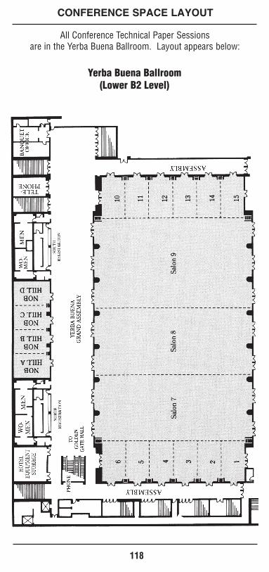
118
CONFERENCE SPACE LAYOUT
All Conference Technical Paper Sessions are in the Yerba Buena Ballroom. Layout appears below:
Yerba Buena Ballroom(Lower B2 Level)
2007_APCover_p117_118.qxp 10/26/2006 12:22 PM Page 4


445 HO
ES
LAN
EP
O B
OX
1331P
ISC
ATA
WA
Y, N
J 08855-1331
ISS
CC
2007 AD
VA
NC
E P
RO
GR
AM
IEEE


![IEEE JOURNAL OF SOLID-STATE CIRCUITS, VOL. 46, NO. 1, JANUARY 2011 …ssl.kaist.ac.kr/2007/data/journal/[2011_JSSC]LongYan.pdf · 2019. 3. 5. · IEEE JOURNAL OF SOLID-STATE CIRCUITS,](https://static.fdocuments.in/doc/165x107/6115b590491e02457105dd76/ieee-journal-of-solid-state-circuits-vol-46-no-1-january-2011-sslkaistackr2007datajournal2011jssc.jpg)