2007 Eckts2 Chapter 14 Output Stages and Power Amplifiers ...
37
CHAPTER 14 2007 Fall: Electronic Circuits 2 CHAPTER 14 Output Stages and Power Amplifiers Deog-Kyoon Jeong dkj @ k dkjeong@snu.ac.kr School of Electrical Engineering S l N ti lU i it Seoul National University
Transcript of 2007 Eckts2 Chapter 14 Output Stages and Power Amplifiers ...

CHAPTER 142007 Fall: Electronic Circuits 2
CHAPTER 14Output Stages and gPower Amplifiers
Deog-Kyoon Jeongdkj @ [email protected]
School of Electrical EngineeringS l N ti l U i itSeoul National University

Introduction
In this chapter, we will be covering…Classification of Output StagesClass A Output StageCl B O t t StClass B Output StageClass AB Output StageBiasing the Class AB CircuitBiasing the Class AB Circuit
11/19/2007 (c) 2007 DK Jeong 2/37
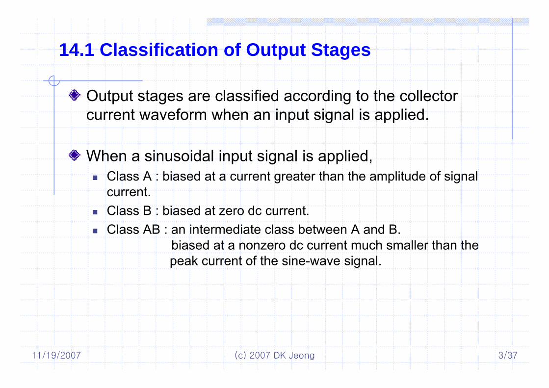
14.1 Classification of Output Stages
Output stages are classified according to the collector current waveform when an input signal is applied.
Wh i id l i i l i li dWhen a sinusoidal input signal is applied,Class A : biased at a current greater than the amplitude of signal currentcurrent.Class B : biased at zero dc current.Class AB : an intermediate class between A and B.
biased at a nonzero dc current much smaller than the peak current of the sine-wave signal.
11/19/2007 (c) 2007 DK Jeong 3/37

14.1 Classification of Output Stages
Collector current waveforms for transistors operating in
(a) class A (b) class B (c) class AB
11/19/2007 (c) 2007 DK Jeong 4/37

14.2 Class A Output Stage - Transfer Characteristic
The emitter follower – the most popular class A ckt.
Figure 14.2 An emitter follower (Q1) biased with a constant current I supplied by transistor Q2.g (Q1) pp y Q2
11/19/2007 (c) 2007 DK Jeong 5/37

14.2 Class A Output Stage - Transfer Characteristic
The bias current must be greater than the largest negative load currentlargest negative load current.
The transfer characteristic is
The positive limit of the linear region is given b
1o I BEv v v= −
by
f
max 1O CC CE satv V V= −
In the negative direction, the limit of the linear region is
v IR or V V= +min 2O L CC CE satv IR or V V= − − +
11/19/2007 (c) 2007 DK Jeong 6/37

14.2 Class A Output Stage - Exercise 14.1
Exercise 14.1 For the emitter follower in the figure below, VCC = 15 V, VCEsat = 0.2 V, VBE=0.7 V, and β is very high. Find the value of R that will establish a bias current sufficiently large to allow the largest possible output signal swing for RL = 1 kΩ. Determine the resulting output signal swing and the minimum and maximum emitter currents.
11/19/2007 (c) 2007 DK Jeong 7/37

14.2 Class A Output Stage - Exercise 14.1
R=?The minimum bias current is given by
| | 14 8V V V− +
Since β is large the current through R
2bias,min
| | 14.8 14.81
CC CE sat
L
V V VI mAR k+
= = =Ω
Since β is large, the current through R = Ibias , so
| | 14 3V V V+ 2
min
| | 14.3 0.9714.8
CC BEV V VR kI mA
− += = = Ω
11/19/2007 (c) 2007 DK Jeong 8/37

14.2 Class A Output Stage - Exercise 14.1
Output signal swing?p g gFor bias current greater than Ibiasmin, the output stage function correctly as long as all BJTs are in linear regionlong as all BJTs are in linear region.
14.8 14.8oV V V− ≤ ≤
Minimum and maximum current?Minimum and maximum current?I E1,max = Ibias,min + iL, max = 29.6 mAI E1 min = 0 AE1,min
11/19/2007 (c) 2007 DK Jeong 9/37

14.2 Class A Output Stage - Signal Waveforms
For sine-wave input, neglecting V th t t ltVCEsat, the output voltage can swing from –VCC to +VCC with the quiescent value being zero.
Since vCE1 = VCC-vo,
11/19/2007 (c) 2007 DK Jeong 10/37

14.2 Class A Output Stage - Signal Waveforms (cont )(cont.)
Assuming that the bias current is l t d t ll iselected to allow a maximum
negative load current of Vcc/RL,
The instantaneous power dissipation in Q1, pD1=vCE1·iC1
11/19/2007 (c) 2007 DK Jeong 11/37

14.2 Class A Output Stage - Power Dissipation
The maximum instantaneous power dissipation in Q1= VCC·I= The quiescent power dissipation in Q1.
Th itt f ll t i t di i t th l t t fThe emitter follower transistor dissipates the largest amount of power when vo=0: The transistor Q1 must be able to withstand a continuous power dissipation of VCC·I.The power dissipation in Q1 depends on the value of RL: When RL=0, a very large current may flow through Q1: short circuit protection is neededprotection is needed.
The maximum instantaneous power dissipation in Q2p p 2=2·VCC·I
11/19/2007 (c) 2007 DK Jeong 12/37

14.2 Class A Output Stage - Power-Conversion EfficiencyEfficiency
Power-Conversion Efficiency of an output stage is defined as
( )( )
LLoad power PS l P
η =
For the emitter follower, the average load power will be
( )SSupply power P
2 2ˆ ˆ
The average (positive + negative) supply power is
2 2( / 2) 12
o oL
L L
V VP
R R= =
The average (positive + negative) supply power is,
Thus, the PCE is, 2S CCP V I=
2ˆ ˆ ˆ1 14 4
o o o
L CC L CC
V V VIR V IR V
η = =
11/19/2007 (c) 2007 DK Jeong 13/37

14.2 Class A Output Stage - Power-Conversion Efficiency (cont)Efficiency (cont)
The maximum efficiency is 25%, obtained when
o CC LV V IR= =
Because 25% is a rather low figure, the class A output stage is rarely used in high-power applications (>1W).
In practice the output voltage swing is limited to lower values to avoid transistors saturation and associated nonlinear distortion. Thus the efficiency achieved is usually in the 10% to 20% rangeusually in the 10% to 20% range.
11/19/2007 (c) 2007 DK Jeong 14/3

14.3 Class B Output Stage
The class B output stage consists of a complementary pare of transistors connected in such a way that both cannot conduct simultaneously.
11/19/2007 (c) 2007 DK Jeong 15/37
Figure 14.5 A class B output stage.

14.3 Class B Output Stage - Circuit Operation
When the input voltage vi is zero, both transistors are cut off – vo is zero.
When vi exceeds about 0.5 V,i ,QN conducts and operates as an emitter follower. v follows vi QP cut offvo follows vi, QP cut off.
When vi goes negative by more than 0.5 V,Q d d iQP conducts and operates as an emitter follower. vo follows vi QN cut off.
The circuit operates in a push-pull fashion.
11/19/2007 (c) 2007 DK Jeong 16/37

14.3 Class B Output Stage - Transfer Characteristic
The transfer characteristic of the class B stage
11/19/2007 (c) 2007 DK Jeong 17/37

14.3 Class B Output Stage - Transfer Characteristic
The dead band results in the crossover distortion.
11/19/2007 (c) 2007 DK Jeong 18/37

14.3 Class B Output Stage - Power-Conversion EfficiencyEfficiency
The average load power will be,2ˆ1
2o
LL
VP R=
The average current drawn from each of the two power supplies will be,
ˆ1 oVP P V
The total supply power will be,
oS S CC
L
P P VRπ+ −= =
ˆ2 oS CC
L
VP V
Rπ=
Thus the PCE is given by
oVπη =
11/19/2007 (c) 2007 DK Jeong 19/37
4 CCVη =

14.3 Class B Output Stage - Power-Conversion Efficiency(cont )Efficiency(cont.)
The maximum efficiency is obtained when is maximum (=VCC-VCESAT≈VCC)oV
At this value of peak output voltage, the PCE is
max 78.5% ( 25% )4
in the class A caseπη = = >>
The maximum average power available from a class B output stage is,2ˆ1 oV
P =2L
L
PR
=
11/19/2007 (c) 2007 DK Jeong 20/37

14.3 Class B Output Stage - Power Dissipation
The quiescent power dissipation of the class B stage is zero.When an input signal is applied, the average power dissipated in the class B stage is given by
D S LP P P= −
Substituting for and for results in2ˆ1
2o
LL
VP
R=
ˆ2 oS CC
L
VP V
Rπ=
D S LP P P
L
2ˆ ˆ2 12
o oD CC
L L
V VP V
R Rπ= −
The maximum average power dissipation is (given by differentiating above eqn )
L L
(given by differentiating above eqn.)2
max 2
2 CCD
L
VPRπ
=
11/19/2007 (c) 2007 DK Jeong 21/37
LRπ

14.3 Class B Output Stage - Power Dissipation (cont )(cont.)
The maximum average power dissipation2
max max 2
2 CCDP DN
L
VP PRπ
= =
11/19/2007 (c) 2007 DK Jeong 22/37
Figure 14.8 Power dissipation of the class B output stage versus amplitude of the output sinusoid.

14.3 Class B Output Stage - Example 14.1
Example 14.1 It is required to design a class B output stage to deliver an average power of 20 W to an 8-Ω load. The power supply is to be selected such that VCC is about 5V greater than the peak output voltage. This avoids transistor saturation and the associated nonlinear distortion, and allows for including short-circuit protection circuitry. Determine the supply voltage required, the peak current drawn from each supply, the total supply power, and the power-conversion efficiency. Also determine the maximum power that each transistor must be able to dissipate safely.
11/19/2007 (c) 2007 DK Jeong 23/37

14.3 Class B Output Stage - Example 14.1
Example 14.1Since
2ˆ1 V
Then
12
oL
L
VP
R=
Then
VRPV LLo 9.172ˆ ==
Therefore we select VCC = 23 V
o
11/19/2007 (c) 2007 DK Jeong 24/37

14.3 Class B Output Stage - Example 14.1
Example 14.1The peak current drawn from each supply is
ARVI o
o 24.2ˆˆ ==
The average power drawn from each supply is
RL
is
1 (2.24 23) 16.4s sP P Wπ+ −= = × =
For a total supply power of 32.8W. The power-conversion efficiency is
π
20 100 61%32 8
LPP
η = = × =
11/19/2007 (c) 2007 DK Jeong 25/37
32.8SP

14.2 Class B Output Stage - Example 14.1
Example 14.1The maximum power dissipated in each transistor is given by,
max max 2CC
DN DPV
P PRπ
= =
2
2
(23) 6.78
LR
W
π
= =2 8π ×
11/19/2007 (c) 2007 DK Jeong 26/37

14.3 Class B Output Stage - Reducing Crossover DistortionDistortion
Reducing crossover distortion by employing a high-gain op amp and overall negative feedback.
The ±0.7 V deadband is reduced to ±0.7/Ao V
11/19/2007 (c) 2007 DK Jeong 27/37
Figure 14.9 Class B circuit with an op amp connected in a negative-feedback loop to reduce crossover distortion.

14.3 Class B Output Stage - Single-Supply OperationOperation
Class B operation from a single power supply
Figure 14.10 Class B output stage operated with a single power supply.
11/19/2007 (c) 2007 DK Jeong 28/37
g p g p g p pp y

14.4 Class AB Output Stage
Crossover distortion can be virtually eliminated by biasing the complementary output transistors at a small nonzero current.
Figure 14.11 Class AB output stage. A bias voltage VBB is applied between the bases of QN and QP, giving rise to a bias current IQ given
11/19/2007 (c) 2007 DK Jeong 29/37
g p g g BB pp QN QP, g g Q gby Eq. (14.23). Thus, for small vI, both transistors conduct and crossover distortion is almost completely eliminated.

14.4 Class AB Output Stage - Circuit Operation
When vI goes positive, the output becomes positive at almost equal valueat almost equal value,
2BB
O I BENVv v v= + −
vO causes a current iL to flow through RL, and iNmust increase
N P Li i i= +
Since the VBB voltage remains constant, the increase in vBEN will result in an equal decrease in vEBP and in iP. The relationship between iN and iP is,vEBP and in iP. The relationship between iN and iP is,
ln ln 2 ln
BEN EBP BB
QN P
v v VIi i
V V V
+ =
⎛ ⎞⎛ ⎞ ⎛ ⎞+ ⎜ ⎟⎜ ⎟ ⎜ ⎟
2
2 2
ln ln 2 ln
0
QN PT T T
S S S
N P Q
V V VI I I
i i I
i i i I
+ = ⎜ ⎟⎜ ⎟ ⎜ ⎟⎝ ⎠ ⎝ ⎠ ⎝ ⎠
=
∴
11/19/2007 (c) 2007 DK Jeong 30/37
2 2 0N L N Qi i i I∴ − − =

14.4 Class AB Output Stage - Circuit Operation (cont )(cont.)
Transfer characteristic of the class AB stageFor small vI, both transistors conduct, and as vI is increased or decreased, one of the two transistors takes over the operation→ crossover distortion is eliminated→ crossover distortion is eliminated
11/19/2007 (c) 2007 DK Jeong 31/37

14.4 Class AB Output Stage - Output Resistance
The output resistance of the class AB b d i d f llcan be derived as follows
||out eN ePR r rV V=
,
||
T TeN eP
N P
T T T
V Vr r
i iV V V
R
= =
∴ = =
The output resistance remains approximately constant in the region
||outN P P N
Ri i i i
∴ = =+
approximately constant in the region around vI=0.At larger load currents, Routdecreases as the load current increases.
11/19/2007 (c) 2007 DK Jeong 32/3

14.4 Class AB Output Stage - Problem 14.16
Problem 14.16 Design the quiescent current of a class AB BJT output stage so that the incremental voltage gain for vi in the vicinity of the origin is in excess of 0.99V/V for loads larger than 100 Ω. Assume that the BJTs have VBE of 0.7V at a current of 100mA and determine the value of VBB required.
The voltage gain of the output stage isThe voltage gain of the output stage isgiven by
Lv RR
RA+
=
Since Av must be greater than 0.99 with R ≥ 100 Ω
outL RR +
with RL ≥ 100 Ω,
Ω≈−≤ 1)11( Lout RA
R
11/19/2007 (c) 2007 DK Jeong 33/37
vA

14.4 Class AB Output Stage - Problem 14.16
Problem 14.16 Rout has a relationship to the circuit parameters, in a way that
Te VrR ==
So the needed IQ to get
Qout I
R22
==
So, the needed IQ to get Rout ≤ 1 Ω is 12.5 mA.
VBB = 2 VBE. Therefore,
VV BEBB 2=
VT ]100
5.12ln7.0[2 +=
11/19/2007 (c) 2007 DK Jeong 34/37
V296.1=

14.5 Biasing The Class AB Circuit - Biasing Using DiodesUsing Diodes
The quiescent current IQ, has the following relationship with IBIAS.
(n denotes the ratio of the emitter-junction area of Q t th j ti f D )Q to the junction area of D.)
BIASQ nII =
n shouldn’t be a large number because IBIAS is drawn into thebecause IBIAS is drawn into the base of QN when its driving a load, thus no current may be left yfor D.
11/19/2007 (c) 2007 DK Jeong 35/37

14.5 Biasing The Class AB Circuit - Biasing Using DiodesUsing Diodes
AdvantageProtection against thermal runaway
DisadvantageVBB’s dependence on the load current
(Thermal runaway: a phenomenon that occurs when the power dissipation of the output stage brings temperature rise to theoutput stage brings temperature rise to the surroundings. The rise in temperature will accommodate more current through BJTs thus forms a positive loop in increasing thethus forms a positive loop in increasing the quiescent current. It will eventually destroy the BJTs.)
11/19/2007 (c) 2007 DK Jeong 36/37

14.5 Biasing The Class AB Circuit - Biasing Using the V MultiplierUsing the VBE Multiplier
(Neglecting base current) R1 and R ill th t IR2 will carry the same current IR, given by
1VI BE=
So, the voltage VBB will be1R
IR =
where
)1(1
21 R
RVV BEBB +=
where
1 RBIASC III −=
1
11 ln
S
CTBE I
IVV =
11/19/2007 (c) 2007 DK Jeong 37/37