2003-10-14 Using RF measurements and simple, empirical...
21
C O N F I D E N T I A L Etch Product Business Group Using RF measurements and simple, empirical plasma models to enhance the performance of dielectric etch systems Steven Shannon, Daniel Hoffman, Jang-Gyoo Yang, Alex Paterson, Theodoros Panagopoulos, John Holland, Dog Buchberger, Brad Mays, Allen Fox, Mike Chafin, Troy Detrick 22 October 2003 56th Gaseous Electronics Conference
Transcript of 2003-10-14 Using RF measurements and simple, empirical...

C O N F I D E N T I A L
Etch Product Business Group
Using RF measurements and simple, empirical plasma models to enhance the performance of dielectric etch systems
Steven Shannon, Daniel Hoffman, Jang-Gyoo Yang, Alex Paterson, Theodoros Panagopoulos, John Holland, Dog Buchberger, Brad Mays, Allen Fox, Mike Chafin, Troy Detrick22 October 200356th Gaseous Electronics Conference

Etch Product Business Group
A more appropriate title slide
Need quick turn-around analysis of plasma processes – especially when customers are involvedNeed simple calculations for results for incorporation into process control algorithmsKey is to not get lost in more complicated details until necessary –start with a simple model and build off of itUsed for customer explanation and simple calculation for process control in etch processes
Focus for this talk – analysis of capacitive coupled plasma etch reactors – RF distributions and simple plasma models
Etch Product Business Group
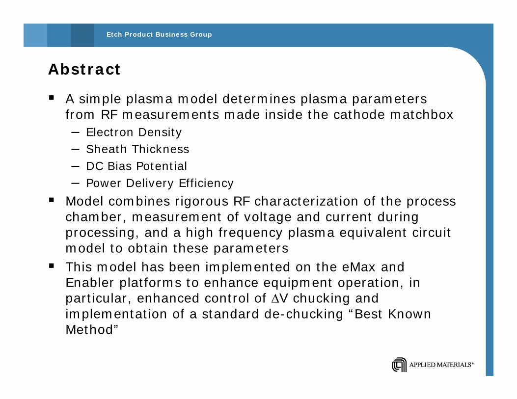
Abstract
A simple plasma model determines plasma parameters from RF measurements made inside the cathode matchbox– Electron Density– Sheath Thickness– DC Bias Potential– Power Delivery Efficiency
Model combines rigorous RF characterization of the process chamber, measurement of voltage and current during processing, and a high frequency plasma equivalent circuit model to obtain these parametersThis model has been implemented on the eMax and Enabler platforms to enhance equipment operation, in particular, enhanced control of ΔV chucking and implementation of a standard de-chucking “Best Known Method”
Etch Product Business Group
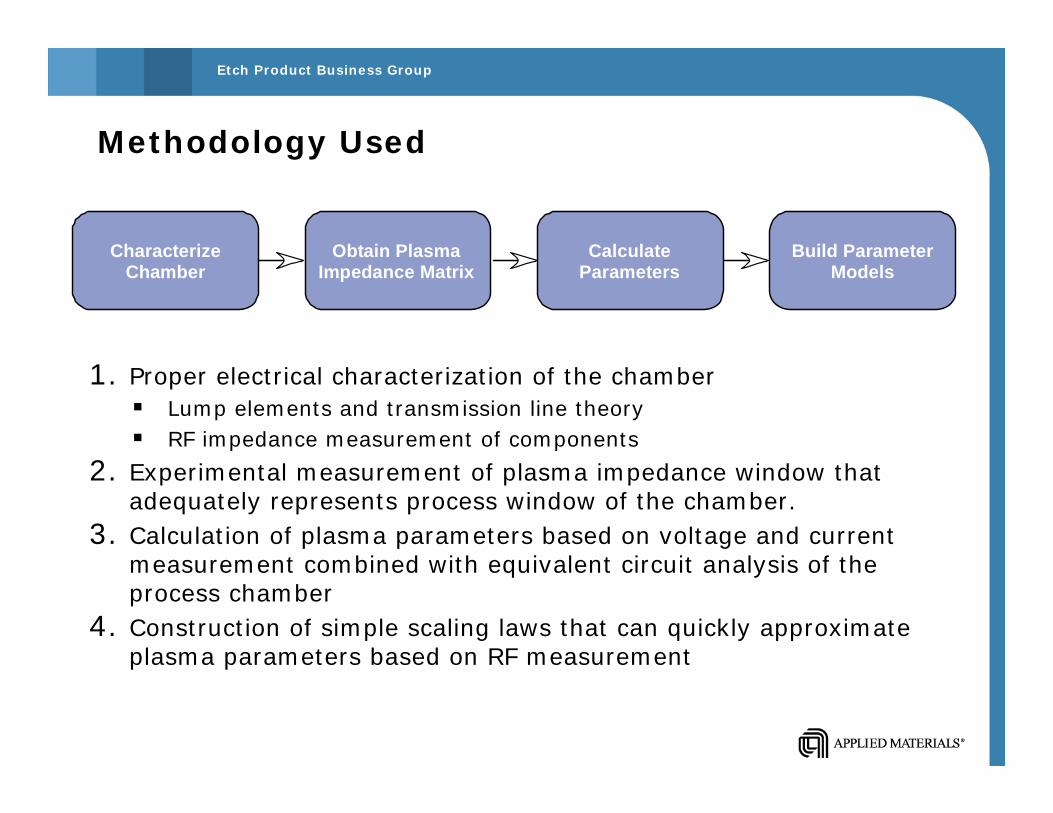
Methodology Used
1. Proper electrical characterization of the chamber Lump elements and transmission line theoryRF impedance measurement of components
2. Experimental measurement of plasma impedance window that adequately represents process window of the chamber.
3. Calculation of plasma parameters based on voltage and current measurement combined with equivalent circuit analysis of the process chamber
4. Construction of simple scaling laws that can quickly approximateplasma parameters based on RF measurement
Build ParameterModels
CalculateParameters
Obtain PlasmaImpedance Matrix
CharacterizeChamber

Etch Product Business Group
Electrical Characterization
RF Generator
Matchbox with VI ProbeMeasure VI for
Process Window
1-Port Impedence Sweepand
Time Domain Reflectometry
NO PLASMA Solve for Plasma Impedences
Calculate Plasma Parameters
Develop Empirical Models Basedon RF measurements (V, I)
RF Generator
Matchbox with VI ProbeControl Plasma ParametersBased on Empirical Models
and VI Measurements
Etch Product Business Group
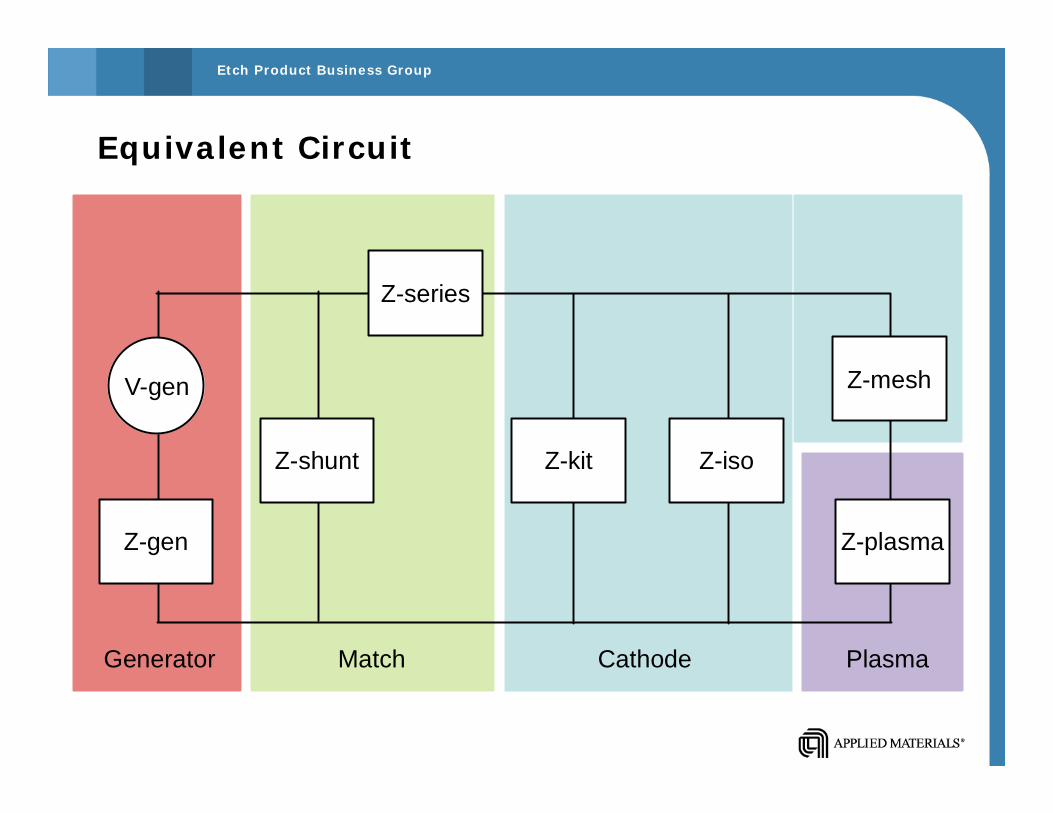
Equivalent Circuit
V-gen
Z-gen
Z-mesh
Z-plasma
Z-isoZ-kit
Z-series
Z-shunt
Generator Match Cathode Plasma

Etch Product Business Group
Plasma Model Problem – Leiberman High Frequency Model with Vacuum Capacitor Sheaths
Cathode
GroundedElectrode
Bulk PlasmaSheaths
Grounded Sheath
Powered Sheath
Z-bulk
Zbulk i C01
i Lp Rp
1−
s0Irf
e ne A.
Cpowered0 A
s0 .
Equivalent ImpedanceMeasured through VI Probe
Need to Solve forne and s0

Etch Product Business Group
Determination of Sheath Thickness and Electron Density:
este
ebulkesheathcalc
AenIs
nZnsZZ
ω=
+=
0
0 )())((
From V,I data at fixed point in the system (along with pressure and power considerations), solve for the current through the total discharge impedance
Solve for ne
Plug in ne and solve for sheaththickness
Break up sheath components into grounded and powered sheathsbased on system asymmetry and x5/2 voltage scaling
Result: electron density and powered sheath thickness profilesas functions of measured RF voltage for constant power
Etch Product Business Group
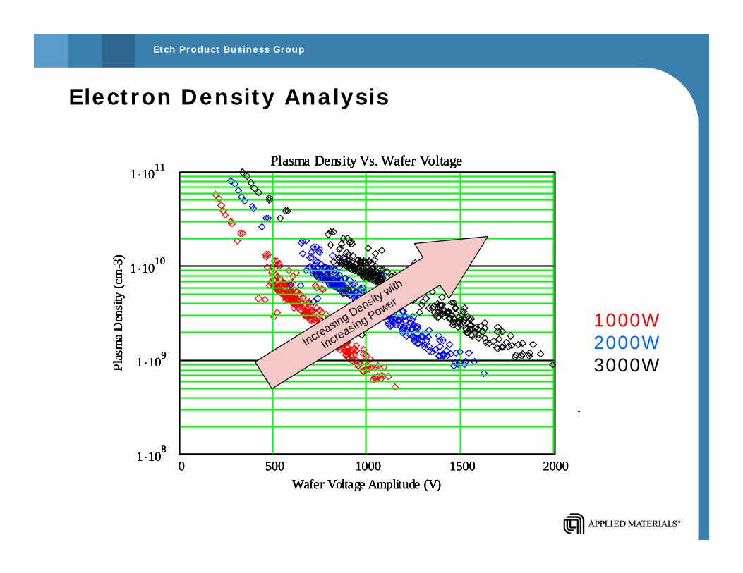
Electron Density Analysis
1000W2000W3000W
0 500 1000 1500 20001 .108
1 .109
1 .1010
1 .1011 Plasma Density Vs. Wafer Voltage
Wafer Voltage Amplitude (V)
Plas
ma
Den
sity
(cm
-3)
.
0 500 1000 1500 20001 .108
1 .109
1 .1010
1 .1011 Plasma Density Vs. Wafer Voltage
Wafer Voltage Amplitude (V)
Plas
ma
Den
sity
(cm
-3)
.
0 500 1000 1500 20001 .108
1 .109
1 .1010
1 .1011 Plasma Density Vs. Wafer Voltage
Wafer Voltage Amplitude (V)
Plas
ma
Den
sity
(cm
-3)
.
Increasing Densitywith
Increasing Power

Etch Product Business Group
Comparison to Langmuir Probe Measurement
13.56MHz and 60MHz power sweep matrix run at two separate pressuresLangmuir probe with passive RF compensation (Scientific Systems Smart Probe)Sufficient ground reference in chamberMeasurements taken at the center of the dischargeResults compared with density obtained at calculated on wafer RF voltage for 13.56MHz power curve
ENIVI Probe
13MHzMatch
13MHzDrive
60MHzDrive

Etch Product Business Group
Measured Density Vs. Calculated Density
1.00E+08
1.00E+09
1.00E+10
1.00E+11
0 5 10 15 20
Run Number
Den
sity
(cm
-3)
Langmuir ProbeRF Model

Etch Product Business Group
Sheath Thickness Analysis
1000W2000W3000W
0 500 1000 1500 20000
0.5
1
Dark Space Thickness Vs. Wafer Voltage
Wafer Voltage Magnitude (V)
Dar
kSp
ace
Thic
knes
s(c
m)
.
0 500 1000 1500 20000
0.5
1
Dark Space Thickness Vs. Wafer Voltage
Wafer Voltage Magnitude (V)
Dar
kSp
ace
Thic
knes
s(c
m)
.
0 500 1000 1500 20000
0.5
1
Dark Space Thickness Vs. Wafer Voltage
Wafer Voltage Magnitude (V)
Dar
kSp
ace
Thic
knes
s(c
m)
.A
tConstantW
aferVoltageIncreasing
Pow
erDecreases
Sheath
Thickness
Etch Product Business Group
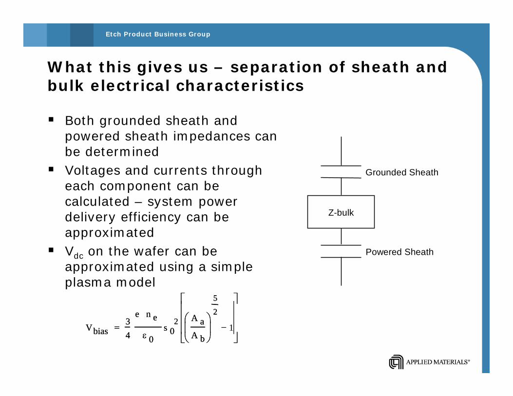
What this gives us – separation of sheath and bulk electrical characteristics
Both grounded sheath and powered sheath impedances can be determinedVoltages and currents through each component can be calculated – system power delivery efficiency can be approximatedVdc on the wafer can be approximated using a simple plasma model
Grounded Sheath
Powered Sheath
Z-bulk
Vbias34
e n e
ε 0s 0
2 A aA b
⎛⎜⎝
⎞⎟⎠
5
2
1−
⎡⎢⎢⎢⎣
⎤⎥⎥⎥⎦
=Vbias34
e n e
ε 0s 0
2 A aA b
⎛⎜⎝
⎞⎟⎠
5
2
1−
⎡⎢⎢⎢⎣
⎤⎥⎥⎥⎦
=

Etch Product Business Group
Allows for more accurate calculation of on wafer RF and DC voltages – captures non-linearity between DC voltage and RF voltage at matchbox
0 200 400 600 800 1000 1200 140030
40
50
60
70
80Old Vs. New Wafer Voltage Difference
"Old" Vrf Measurement (V)
Erro
r in
Old
Mea
sure
men
t (V
)
.

Etch Product Business Group
Application - ΔV electrostatic chucking
DC voltage applied causes charge separation induced force to hold wafer to work pieceInduced DC potential from plasma has to be corrected for to provide consistent force chucking from process to processInaccurate representation of induced plasma potential results in variable chucking force from process to process
Monopolar Electrostatic Chuck
Embedded mesh with appliedDC voltage V
Plasma Discharge
Wafer
V Generatedby Plasma

Etch Product Business Group
Experimental Assessment of Vdc Prediction
Tested on eMax CT’ MERIE chamber over large pressure, power, and B-Field window for numerous dielectric etch processesΔV is controlled across electrostatic chuck (presumably referenced from DC plasma potentialIf reference potential is correct, all processes should have identical VI characteristics as ΔV is varied
ENIVI Probe
13MHzMatch
13MHzDrive
Monopolar Electrostatic Chuck
Embedded mesh with appliedDC voltage V
Plasma Discharge
Wafer
V Generatedby Plasma

Etch Product Business Group
Accurate representation of DC potential results in more consistent tool performance
Using Vrf CompensationUsing Vdc Obtained from Model
0 200 400 600 800 1000 1200 140030
40
50
60
70
80Old Vs. New W afer Voltage Difference
"Old" Vrf Measurement (V)
Erro
rin
Old
Mea
sure
men
t(V
) .
Iesc Vs V Setting
-160
-140
-120
-100
-80
-60
-40
-20
0
20
-500 -450 -400 -350 -300 -250 -200 -150 -100
V (Volts)
More Consistant Chucking RealizedUsing Simple Plasma Model
Same chucking voltage can nowbe used on ALL eMax CT’ Processes
Process Dependent Chucking Voltagewas a TOP concern at several
customer sites - NOW RESOLVED

Etch Product Business Group
Conclusions
Rigorous RF characterization of process chambers, combined with simple plasma models, can provide good first estimates of plasma parameters, including electron density, sheath thickness, and DC potentialsUsing these simple models, Applied Materials dielectric etch chambers have been able to standardize chucking and de-chucking of wafers for all processes and use non-evasive, low cost techniques to characterize their plasma discharges

Etch Product Business Group
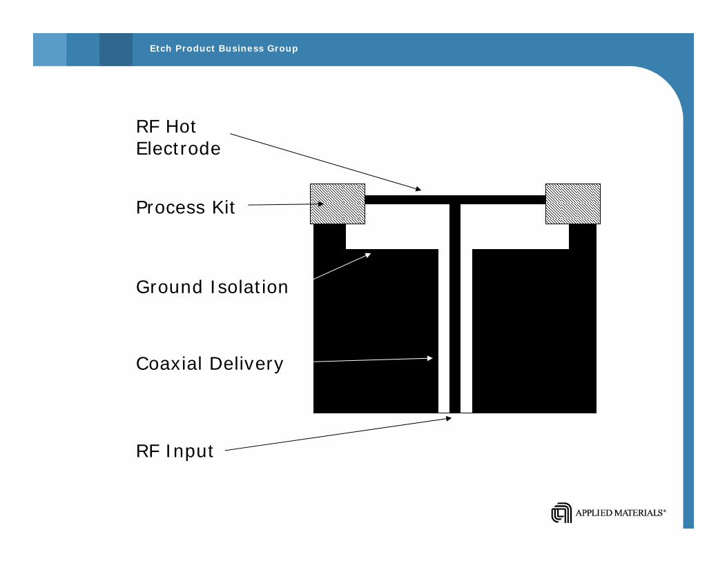
Etch Product Business Group
RF Input
Ground Isolation
RF HotElectrode
Process Kit
Coaxial Delivery

Etch Product Business Group
Iesc Vs KVSP
-160
-140
-120
-100
-80
-60
-40
-20
0
20
-600 -500 -400 -300 -200 -100 0
KVSP (Volts)
Iesc
(mic
roam
ps)
Blue = Empirical ModelRed = Vrf Scaling