2 LDO Regulat or with Voltage Detector and Watchdog...
30
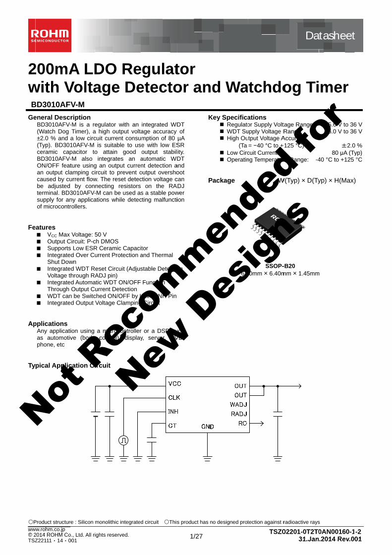
〇P . © 2 TSww 2 w B Ge Fe Ap Ty Product structure 2014 ROHM Co Z22111・14・0 ww.rohm.co.jp 200mA with V BD3010AFV eneral Descr BD3010AFV- (Watch Dog ±2.0 % and a (Typ). BD301 ceramic cap BD3010AFV- ON/OFF feat an output cla caused by cu be adjusted terminal. BD3 supply for an of microcontr eatures ■ V CC Max ■ Output C ■ Supports ■ Integrate Shut Dow ■ Integrate Voltage th ■ Integrate Through ■ WDT can ■ Integrate pplications Any applicati as automotiv phone, etc pical Applic e : Silicon mono o., Ltd. All rights 001 A LDO V oltag V -M ription -M is a regula Timer), a hig a low circuit c 10AFV-M is s pacitor to a -M also inte ture using an amping circuit urrent flow. Th by connect 3010AFV-M ca ny application rollers. Voltage: 50 V Circuit: P-ch DM s Low ESR Ce d Over Curren wn d WDT Reset hrough RADJ d Automatic W Output Curren n be Switched d Output Volta ion using a m ve (body con cation Circu olithic integrated reserved. O Re ge De ator with an h output volta current consum suitable to use ttain good o egrates an a output curren t to prevent o he reset detec ing resistors an be used as s while detec V MOS eramic Capacit nt Protection a Circuit (Adjus pin) WDT ON/OFF nt Detection ON/OFF by U age Clamping microcontroller ntrol), display it d circuit 〇This gulat etecto integrated WD age accuracy mption of 80 e with low ES output stabil automatic WD nt detection a output oversho ction voltage c on the RA s a stable pow cting malfuncti tor and Thermal stable Detectio Function Using INH Pin Circuit or a DSP su y , server, DV s product has n 1/27 tor or and DT of μA SR ity. DT and oot can ADJ wer ion on uch VD, K P o designed prot d Wa Key Specifica Regulato WDT Su High Ou (Ta Low Circ Operatin ackage 6.5 tection against r TSZ0 tchdo ations or Supply Volt upply Voltage R tput Voltage A = −40 °C to + cuit Current: ng Temperatur W SSOP- 50mm × 6.40m Da radioactive rays 31.Jan 02201-0T2T0 og Ti tage Range: Range: Accuracy: +125 °C) re Range: -4 W(Typ) × D(Ty -B20 mm × 1.45mm atasheet s .2014 Rev.0 0AN00160-1 mer 5.6 V to 36 6.0 V to 36 ±2.0 80 μA (Ty 40 °C to +125 yp) × H(Max) m t 01 -2 6 V 6 V 0 % yp) °C ) Not Recommended for New Designs
Transcript of 2 LDO Regulat or with Voltage Detector and Watchdog...
〇P
. © 2TSZ
ww
2wB
Ge
Fe
Ap
Ty
Product structure
2014 ROHM CoZ22111・14・0
ww.rohm.co.jp
200mAwith VBD3010AFV
eneral DescrBD3010AFV-(Watch Dog ±2.0 % and a(Typ). BD301ceramic capBD3010AFV-ON/OFF featan output clacaused by cube adjusted terminal. BD3supply for anof microcontr
eatures VCC Max Output C Supports Integrate
Shut Dow Integrate
Voltage th Integrate
Through WDT can Integrate
pplications Any applicatias automotivphone, etc
pical Applic
e : Silicon mono
o., Ltd. All rights 001
A LDOVoltag
V-M
ription -M is a regulaTimer), a higa low circuit c10AFV-M is spacitor to a-M also inteture using an amping circuiturrent flow. Th
by connect3010AFV-M cany applicationrollers.
Voltage: 50 VCircuit: P-ch DMs Low ESR Ced Over Curren
wn d WDT Reset hrough RADJ d Automatic WOutput Curren
n be Switched d Output Volta
ion using a mve (body con
cation Circu
olithic integrated
reserved.
O Rege De
ator with an h output volta
current consumsuitable to usettain good o
egrates an aoutput curren
t to prevent ohe reset detecing resistors an be used ass while detec
V MOS eramic Capacitnt Protection a
Circuit (Adjuspin)
WDT ON/OFF nt Detection ON/OFF by U
age Clamping
microcontroller ntrol), display
it
d circuit 〇This
gulatetecto
integrated WDage accuracy mption of 80 e with low ESoutput stabilautomatic WDnt detection aoutput overshoction voltage c
on the RAs a stable powcting malfuncti
tor and Thermal
stable Detectio
Function
Using INH PinCircuit
or a DSP suy, server, DV
s product has n
1/27
tor or and
DT of
µA SR ity. DT
and oot can ADJ wer ion
on
uch VD,
K
P
o designed prot
d Wa
Key Specifica Regulato WDT Su High Ou
(Ta Low Circ Operatin
ackage
6.5
tection against r
TSZ0
tchdo
ations or Supply Voltupply Voltage Rtput Voltage A= −40 °C to +
cuit Current: ng Temperatur
W
SSOP-50mm × 6.40m
Data
radioactive rays
31.Jan02201-0T2T0
og Ti
tage Range: Range:
Accuracy: +125 °C)
re Range: -4
W(Typ) × D(Ty
-B20 mm × 1.45mm
Datasheet
s
.2014 Rev.00AN00160-1
mer
5.6 V to 366.0 V to 36
±2.080 μA (Ty
40 °C to +125
yp) × H(Max)
m
eet
01-2
6 V 6 V
0 % yp) °C
)
Not R
ecom
men
ded
for
New D
esig
ns

BD Datasheet
© 2ww
TSZ
Pin Pin
Blo
D3010AFV Datasheet
2014 ROHM Coww.rohm.com
Z22111・15・0
n Configura
n Descriptio
Pin No. Pin
1 V
2 N
3 G
4 G
5 G
6 G
7 G
8 C
9
10
ock Diagram
V-M Datasheet
o., Ltd. All rights 001
ation
on
n Name
VCC Powe
N.C. -
GND
GND
GND
GND
GND
GND
CLK Clock
INH WDT
CT Exterdelayconn
m
VCC
N.C.
GND
GND
GND
CLK
INH
CT
GND
GND
Datasheet
reserved.
Fun
er supply pin
D
k input from m
T ON / OFF fun
rnal capacitany time, WDT mection pin
OCP
Edge
ON/OFF Circuit
PREREG
VREF_R
Datasheet
ction
microcontroller
nction pin
ce for reset oumonitor time se
V
VREF
TSD
R
2/27
Datasheet
Pin N
11
12
13
14
15
16
17
18
19
utput etting 20
For
VthH VthL
(TOP VIEW)
Datasheet
No. Pin Name
RO
RADJ
WADJ
GND
GND
GND
GND
GND
OUT
OUT
rced Monitor
Stand-by
WDT
OUT
Datasheet
TSZ0
e
Reset outpu
Reset detec
WDT opera
GND
Voltage outp
VREF_R
VCLP
VCC
Datasheet
02201-0T2T031.Jan
Function
ut pin
ction voltage s
ating current se
put pin
RO
RADJ
WADJ
GND
GND
GND
GND
OUT
OUT
GND
DatasheDatasheet
0AN00160-1.2014 Rev.00
set pin
et pin
eetDatasheet
-201
Not R
ecom
men
ded
for
New D
esig
ns

BD3010AFV-M
3/27
DatasheetDatasheet
© 2014 ROHM Co., Ltd. All rights reserved. www.rohm.com
TSZ22111・15・001
TSZ02201-0T2T0AN00160-1-231.Jan.2014 Rev.001
Absolute Maximum Ratings (Ta = 25 °C)
Parameter Symbol Rating Unit
Supply Voltage (Note 1) VCC -0.3 to +50 V
VADJ Set Pin Voltage VRADJ -0.3 to +7 V
Regulator Output Pin Voltage VOUT -0.3 to +7 V
INH Pin Voltage VINH -0.3 to +15 V
Reset Output Pin Voltage VRO -0.3 to +7 V
Watchdog Input Pin Voltage VCLK -0.3 to +15 V
Watchdog Time Set Pin Voltage VCT -0.3 to +7 V
Watchdog Operation Current Set Pin Voltage VWADJ -0.3 to +7 V
Power Dissipation (Note 2) Pd 1.25 W
Operating Temperature Range Topr -40 to +125 °C
Storage Temperature Range Tstg -55 to +150 °C
Maximum Junction Temperature Tjmax 150 °C
(Note 1) Should not exceed Pd. (Note 2) Reduced by 10.0 mW / °C over Ta = 25 °C, when mounted on 70 mm × 70 mm × 1.6 mm glass epoxy board: Caution: Operating the IC over the absolute maximum ratings may damage the IC. The damage can either be a short circuit between pins or an open circuit
between pins and the internal circuitry. Therefore, it is important to consider circuit protection measures, such as adding a fuse, in case the IC is operated over the absolute maximum ratings.
Recommended Operating Conditions (Ta = -40 °C to +125 °C)
Parameter Symbol Min Max Unit
Supply Voltage (Note 3) VCC 5.6 36.0 V
Supply Voltage (Note 4) VCC 6.0 36.0 V
Output Current IOUT 0 200 mA
(Note 3) For the output voltage, consider the voltage drop (dropout voltage) due to the output current. (Note 4) Operating condition for automatic WDT ON / OFF.
Not R
ecom
men
ded
for
New D
esig
ns
BD3010AFV-M
4/27
DatasheetDatasheet
© 2014 ROHM Co., Ltd. All rights reserved. www.rohm.com
TSZ22111・15・001
TSZ02201-0T2T0AN00160-1-231.Jan.2014 Rev.001
Electrical Characteristics (Unless otherwise specified, Ta = -40 °C to +125 °C, VCC = 13.5 V, INH = 5 V, CLK = GND, IOUT = 0 mA)
Parameter Symbol Min Typ Max Unit Conditions
[Entire Device]
Circuit Current 1 ICC1 - 80 140 µA
Circuit Current 2 ICC2 - 110 170 µA IOUT = 50 mA (Ta = 25 °C)
[Regulator]
Output Voltage VOUT 4.90 5.00 5.10 V
Line Regulation Line.Reg - 5 30 mV VCC = 5.6 V to 36 V
Load Regulation Load.Reg - 20 60 mV IOUT = 5 mA to 150 mA
Dropout Voltage ΔVD - 0.25 0.50 V VCC = 4.75 V, IOUT = 150 mA
Ripple Rejection R.R. 45 55 - dB f = 120 Hz, EIN = 1 Vrms,IOUT = 100 mA
WADJ Mirror Current Ratio ΔI 0.002 0.010 0.025 - IOUT = 50 mA (output)
Output Voltage Clamp (Comparator) VCLP 5.2 5.5 5.8 V IOUT = 20 mA (input)
[Reset]
Detection Voltage VDET 4.12 4.25 4.38 V RADJ = Open
Hysteresis Width VHYS 35 70 150 mV
Output Delay Time L to H (Power On Reset) tdLH 1.8 2.3 2.8 ms VOUT = VDET ± 0.5 V, CCT = 0.01 µF
Low Output Voltage VRST - 0.1 0.4 V VOUT = 4.0 V
Minimum Operating Voltage VOPL 1.5 - - V
[Watchdog Timer]
Upper Switching Threshold Voltage VthH 1.08 1.15 1.25 V WDT ON, INH = Open
Lower Switching Threshold Voltage VthL 0.13 0.15 0.17 V WDT ON, INH = Open
WDT Charge Current ICTC 3.5 5.0 6.5 µA WDT ON, INH = Open, VCT = 0 V
WDT Discharge Current ICTD 0.8 1.3 1.7 µA WDT ON, INH = Open,VCT = 1.3 V
WDT Watch Time (Note 5) tWH 6.4 8.0 9.6 ms WDT ON, INH = Open, CCT = 0.01 µF (Ceramic Cap) WDT Reset Time (Note 5) tWL 1.6 2.0 2.4 ms
WDT Operating Current (Note 6) IOA 0.3 1.7 4.0 mA WDT ON, INH open, 5 kΩ resistor is placed between WADJ and OUT pins.
[INH]
WDT OFF Threshold Voltage VHINH VOUT
×0.8 - VOUT V
WDT ON Threshold Voltage VLINH 0 - VOUT
×0.3 V Pulled down inside the IC when
INH = open
INH Input Current IINH - 15 30 µA VINH = 5 V
[CLK]
CLK OFF Threshold Voltage VLCLK 0 - VOUT
×0.3 V
CLK ON Threshold Voltage VHCLK VOUT
×0.8 - VOUT V
CLK Input Pulse Width tWCLK 500 - - ns
(Note 5) Characteristics of ceramic cap not considered. (Note 6) Characteristics of external resistor not considered.
Not R
ecom
men
ded
for
New D
esig
ns

BD3010AFV-M
5/27
DatasheetDatasheet
© 2014 ROHM Co., Ltd. All rights reserved. www.rohm.com
TSZ22111・15・001
TSZ02201-0T2T0AN00160-1-231.Jan.2014 Rev.001
Typical Performance Curves (Unless otherwise specified, Ta = 25 °C, VCC = 13.5 V, INH = 5 V, CLK = GND, IOUT = 0 mA)
Figure 1. Circuit Current 1 vs Supply Voltage
Figure 2. Circuit Current 2 vs Output Current
Figure 3. Output Voltage vs Supply Voltage
Figure 4. Output Voltage vs Output Current
0
30
60
90
120
150
180
0 5 10 15 20 25 30 35
Cir
cuit
Cu
rre
nt:
I CC
1[μ
A]
Supply Voltage: VCC [V]
0
1
2
3
4
5
6
0 5 10 15 20 25 30 35
Ou
tpu
t Vo
ltag
e: V
OU
T[V
]
Supply Voltage: VCC [V]
0
1
2
3
4
5
6
0 100 200 300 400 500 600 700
Ou
tpu
t Vo
ltag
e: V
OU
T[V
]
Output Current: IOUT [mA]
Ta = 125 °C
Ta = 25 °C Ta = -40 °C
Ta = -40 °C
Ta = 25 °C
Ta = 125 °C
Ta = 25 °C
Ta = -40 °C Ta = 125 °C
0
0.1
0.2
0.3
0.4
0.5
0 50 100 150 200C
ircu
it C
urr
en
t: I C
C2
[mA
]Output Current: IOUT [mA]
Ta = 25 °C
Not R
ecom
men
ded
for
New D
esig
ns

BD3010AFV-M
6/27
DatasheetDatasheet
© 2014 ROHM Co., Ltd. All rights reserved. www.rohm.com
TSZ22111・15・001
TSZ02201-0T2T0AN00160-1-231.Jan.2014 Rev.001
Typical Performance Curves - Continued (Unless otherwise specified, Ta = 25 °C, VCC = 13.5 V, INH = 5 V, CLK = GND, IOUT = 0 mA)
0.0
0.1
0.2
0.3
0.4
0.5
0.6
0 50 100 150 200
Dro
po
ut V
olta
ge
: ΔV
d[V
]
Output Current: IOUT [mA]
Figure 5. Dropout Voltage vs Output Current(VCC = 4.75 V)
Figure 6. Ripple Rejection vs Frequency
(ein = 1 Vrms, IO = 100 mA)
Figure 7. Output Voltage vs Ambient Temperature
Figure 8. Output Voltage vs Ambient Temperature
0
20
40
60
80
10 100 1000 10000 100000 1000000R
ipp
le R
eje
ctio
n: R
.R.
[dB
]
Frequency: f [Hz]
4.90
4.95
5.00
5.05
5.10
-40 0 40 80 120
Ou
tpu
t Vo
ltag
e: V
OU
T [V
]
Ambient Temperature: Ta [°C]
0
1
2
3
4
5
6
100 120 140 160 180 200
Ou
tpu
t Vo
ltag
e: V
OU
T[V
]
Ambient Temperature: Ta [°C]
150 °C
Ta = 25 °C
Ta = 125 °C
Ta = 125 °C
Ta = 25 °C
Ta = -40 °C
170 °C
Ta = -40 °C
Not R
ecom
men
ded
for
New D
esig
ns

BD3010AFV-M
7/27
DatasheetDatasheet
© 2014 ROHM Co., Ltd. All rights reserved. www.rohm.com
TSZ22111・15・001
TSZ02201-0T2T0AN00160-1-231.Jan.2014 Rev.001
Figure 12. WDT Time vs Ambient Temperature
(CCT = 0.01 µF, VCC = 5 V, INH = Open)
Typical Performance Curves – continued (Unless otherwise specified, Ta = 25 °C, VCC = 13.5 V, INH = 5 V, CLK = GND, IOUT = 0 mA)
-5.0
-4.0
-3.0
-2.0
-1.0
0.0
1.0
2.0
0 0.3 0.6 0.9 1.2 1.5C
T P
in C
urr
en
t: I C
TC,I C
TD
[μA
]
CT Pin Voltage: VCT [V]
0
1
2
3
4
5
6
7
8
9
-40 0 40 80 120
WD
T T
ime
: tW
L, t
WH
[ms]
Ambient Temperature: Ta [°C]
Figure 9. Reset Output vs Output Voltage
(RADJ = Open)
Figure 10. CT Pin Current vs CT Pin Voltage
(VCC = 5 V, INH = Open)
Figure 11. Reset DET Voltage vs Ambient Temperature
0
1
2
3
4
5
0 1 2 3 4 5
Re
set
Ou
tpu
t: V
RO
[V]
Output Voltage: VOUT [V]
4.0
4.1
4.2
4.3
4.4
4.5
-40 0 40 80 120
Re
set
DE
T V
olta
ge
: VD
ET
[V]
Ambient Temperature: Ta [°C]
Ta = 25 °C
Ta = 125 °C
Ta = -40 °C
Ta = 125 °C
Ta = -40 °C
Ta = 25 °C
VHYS
VDET
Watch time
Reset time
Not R
ecom
men
ded
for
New D
esig
ns
BD3010AFV-M
8/27
DatasheetDatasheet
© 2014 ROHM Co., Ltd. All rights reserved. www.rohm.com
TSZ22111・15・001
TSZ02201-0T2T0AN00160-1-231.Jan.2014 Rev.001
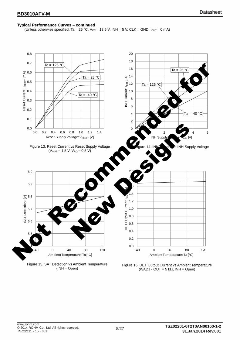
Figure 13. Reset Current vs Reset Supply Voltage
(VOUT = 1.5 V, VRO = 0.5 V)
Figure 14. INH Current vs INH Supply Voltage
Figure 15. SAT Detection vs Ambient Temperature
(INH = Open)
Typical Performance Curves – continued (Unless otherwise specified, Ta = 25 °C, VCC = 13.5 V, INH = 5 V, CLK = GND, IOUT = 0 mA)
0.0
0.1
0.2
0.3
0.4
0.5
0.6
0.7
0.8
0.0 0.2 0.4 0.6 0.8 1.0 1.2 1.4
Re
set
Cu
rre
nt :
IR
ES
ET
[mA
]
Reset Supply Voltage: VRESET [V]
0
2
4
6
8
10
12
14
16
18
20
0 1 2 3 4 5
INH
Cu
rre
nt:
I IN
H[μ
A]
INH Supply Voltage: VINH [V]
Figure 16. DET Output Current vs Ambient Temperature
(WADJ - OUT = 5 kΩ, INH = Open)
5.4
5.5
5.6
5.7
5.8
5.9
6.0
-40 0 40 80 120
SA
T D
ete
ctio
n:
[V]
Ambient Temperature: Ta [°C]
Ta = 25 °C
Ta = 125 °C
Ta = -40 °C
Ta = 25 °C
Ta = 125 °C
Ta = -40 °C
0.0
0.2
0.4
0.6
0.8
1.0
1.2
1.4
1.6
1.8
2.0
-40 0 40 80 120
DE
T O
utp
ut
Cu
rre
nt:
I OA
[mA
]
Ambient Temperature: Ta [°C]Not R
ecom
men
ded
for
New D
esig
ns

BD3010AFV-M
9/27
DatasheetDatasheet
© 2014 ROHM Co., Ltd. All rights reserved. www.rohm.com
TSZ22111・15・001
TSZ02201-0T2T0AN00160-1-231.Jan.2014 Rev.001
Figure 17. DET Output Current vs Supply Voltage
(WADJ - OUT = 5 kΩ, INH =Open)
Typical Performance Curves – continued (Unless otherwise specified, Ta = 25 °C, VCC = 13.5 V, INH = 5 V, CLK = GND, IOUT = 0 mA)
-20
-15
-10
-5
0
5
10
15
20
6 11 16 21 26 31 36
DE
T O
utp
ut
Cu
rre
nt:
I OA
[%]
Supply Voltage: VCC [V]
Ta = 25 °C
Not R
ecom
men
ded
for
New D
esig
ns

BD3010AFV-M
10/27
DatasheetDatasheet
© 2014 ROHM Co., Ltd. All rights reserved. www.rohm.com
TSZ22111・15・001
TSZ02201-0T2T0AN00160-1-231.Jan.2014 Rev.001
Measurement Circuit for Electrical Data
Measurement Circuit of Figure1 and Figure 2
Measurement Circuit of Figure3, Figure 7 and Figure 8
Measurement Circuit of Figure 4
Measurement Circuit of Figure 5 Measurement Circuit of Figure 6 Measurement Circuit of Figure9
and Figure 11
Measurement Circuit of Figure 10 Measurement Circuit of Figure 12 Measurement Circuit of Figure 13
Measurement Circuit of Figure 14 Measurement Circuit of Figure 15 Measurement Circuit of Figure16 and Figure 17
IOUT
VCC
N.C
GND
GND
OUT
OUT
GND
GND
GND
GND
GND
WADJ
RADJ
RO
GND
GND
GND
CLK
INH
CT
VCC
N.C
GND
GND
OUT
OUT
GND
GND
GND
GND
GND
WADJ
RADJ
RO
GND
GND
GND
CLK
INH
CT
IOUT
VCC
N.C
GND
GND
OUT
OUT
GND
GND
GND
GND
GND
WADJ
RADJ
RO
GND
GND
GND
CLK
INH
CT
VCC
N.C
GND
GND
OUT
OUT
GND
GND
GND
GND
GND
WADJ
RADJ
RO
GND
GND
GND
CLK
INH
CT
0.01μF
Oscilloscope
VCC
N.C
GND
GND
OUT
OUT
GND
GND
GND
GND
GND
WADJ
RADJ
RO
GND
GND
GND
CLK
INH
CTOscilloscope
Not R
ecom
men
ded
for
New D
esig
ns

BD3010AFV-M
11/27
DatasheetDatasheet
© 2014 ROHM Co., Ltd. All rights reserved. www.rohm.com
TSZ22111・15・001
TSZ02201-0T2T0AN00160-1-231.Jan.2014 Rev.001
RADJ
OUT
R2=815kΩ
R1=330kΩ
R4
R3
OUT
VRADJ ≈1.23V
RO
470kΩ
+ ~ ~
OUT
100Ω 1kΩ
-
Application Information 1. Detection Voltage Adjustment (Resistance Value is Typical Value)
IC Internal Block Diagram
When typical detection voltage is 4.25 V
V /
where: VDET is the reset detection voltage VRADJ is the internal reference voltage (MOS input) R1,R2 is the IC internal resistor (Voltage detection precision is tightened up to ±3 % by laser-trimming R1 and R2)
VRADJ will fluctuate 1.23 V ±6.0 % Insert pull down resistor R3 (lower resistance than R1) in between RADJ-GND, and pull-down resistor R4 (lower resistance than R2) in between RADJ-OUT to adjust the detection voltage. By doing so, the detection voltage can be adjusted using the formula below.
V / / / / When the output resistance value is as small enough to ignore the IC internal resistance, you can find the detection voltage by the formula below.
V /
Adjust the resistance value by application as the circuit current increases due to the added resistor.
Not R
ecom
men
ded
for
New D
esig
ns

BD3010AFV-M
12/27
DatasheetDatasheet
© 2014 ROHM Co., Ltd. All rights reserved. www.rohm.com
TSZ22111・15・001
TSZ02201-0T2T0AN00160-1-231.Jan.2014 Rev.001
2. WDT Voltage Detection (Resistance Value is Typical Value ) WDT can be automatically switched ON/OFF by the output load current. To detect the output load current, insert a resistor between OUT-WADJ. Current detection is adjustable by varying the resistance value from 1 kΩ to 15 kΩ. Calculation: IOUT (Desired load current value) × ΔI (WADJ current mirror ratio)
× (external R / 140 kΩ (Note 1)) ≥ 100 mV (Note 2)
(Note 1) is the IC internal resistance between WADJ - OUT (tolerance approx ±30 %, temperature coefficient approx 2000 ppm) (Note 2) is an offset of the detection comparator (tolerance approx 100 mV ±10 %)
When there is no resistor between WADJ - OUT, IOUT = 70 µA can be detected by the formula below IOUT (Desired load current value) × ΔI (WADJ current mirror ratio) × 140 kΩ ≥ 100 mV
(Note) If the OUT - WADJ resistance value is not same as the condition on the electrical characteristics table, i.e. 5 KΩ,
choose the resistance value in ratio referring to the above equation.
<Timing Chart> Timing Chart on no load condition (Stand-by Mode)
LOW
HIGH
WDT ON
WDT OFF
140kΩ
+
+
PowTr OUT
WADJ
WADJ-R (External R)
IC Internal Block Diagram
-
-
Not R
ecom
men
ded
for
New D
esig
ns

BD3010AFV-M
13/27
DatasheetDatasheet
© 2014 ROHM Co., Ltd. All rights reserved. www.rohm.com
TSZ22111・15・001
TSZ02201-0T2T0AN00160-1-231.Jan.2014 Rev.001
3. Power ON Reset Power ON reset (output delay time) is adjustable by CT pin capacitor.
1.15 /
where: tdLH is the output delay time ( power ON reset) 1.15V is the upper switching threshold voltage (Typ) CTcapacitance is the capacitor connected to CT pin ICTCis the WDT charge current
<Calculation example > with 0.01 µF CT pin capacitor
1.15 0.01 /5.0 2.3
If the CT capacitance is not the same as the condition on the electrical characteristics table, i.e., 0.01 µF, choose the
capacitance value in ratio referring to the above equation.
<Timing Chart> Note: Watchdog Timer OFF (INH ON)
4.0V
4.0V
CT pull up voltage
4.0V
0V
13.5V
5V
0V
0V
1.25V1.15V
0V
0V
0V
OUTvoltage
0mA
3V
5V
CT
CLK
RO
VCC
OUT
INH
IOUT
4.25V VHYS70mV
4.32V
Reset ONOutput delay time(Power ON reset)
Reset ONReset ONOutput delay time
(Power ON reset)Not R
ecom
men
ded
for
New D
esig
ns
BD3010AFV-M
14/27
DatasheetDatasheet
© 2014 ROHM Co., Ltd. All rights reserved. www.rohm.com
TSZ22111・15・001
TSZ02201-0T2T0AN00160-1-231.Jan.2014 Rev.001
4. Watchdog Timer Watch Dog Timer (WDT watch time, reset time) is adjustable by the CT pin capacitor
1.00 /
1.00 /
where: tWH is the WDT watch time (delay time to turn the reset ON) tWL is the WDT reset time (time the reset is ON) 1.00V is the upper switching threshold voltage - lower switching threshold voltage CTcapacitance is the CT pin capacitor (Shared with power ON reset) ICTC is the WDT charge current ICTD is the WDT discharge current
WDT time’s accuracy is ±20 % by trimming
<Calculation example > with 0.01 µF CT pin capacitor
1.00 0.01 /1.3 8.0
1.00 0.01 /5.0 2.0
If the CT capacitance is not the same as the condition on the electrical characteristics table, choose the capacitance value in ratio referring to the above equation.
<Timing Chart>
0V
13.5V
5V
0V
1.25V1.15V
0V
OUTvoltage
CT
CLK
Ro
VCC
OUT
INH
IOUT
WDT watch time
WDT reset time
Detection of rising edge
Stand by mode
0mA
Detectivecurrent
5mA
5V
0V
0.15V
0V
5V
0V
WDT watch ONby load ON
WDT watch OFF by INH ON
CT switch from discharging to dischargingby CLK edge recognition.
Does not accept less than 500 nsec
TWCLK
Not R
ecom
men
ded
for
New D
esig
ns

BD3010AFV-M
15/27
DatasheetDatasheet
© 2014 ROHM Co., Ltd. All rights reserved. www.rohm.com
TSZ22111・15・001
TSZ02201-0T2T0AN00160-1-231.Jan.2014 Rev.001
LOW
WDT ON
WDT OFF
HIGH
INH ON/OFF
Current CT 300kΩ
VREF_R (Typ≈1.25V)
External Capacitor
10kΩ
5. WDT timer ON / OFF Switch INH (Resistance Value is Typical Value) BD3010AFV-M has a switch INH to turn the WDT ON / OFF
IC Internal Block Diagram
By using INH ON, CT voltage can be pulled up to internal voltage VREF_R (invalid with power ON reset)
<Timing Chart>
CT
CLK
RO
VCC
OUT
INH
IOUT
13.5V
0V
5V
0V
5V
0V
1.25V1.15V
0.15V
0V
5V
0V
0V
OUTvoltage
5mA
0mA
Watch mode ON
CT pull up voltageVthH
VthL
INH ON during charging CT.Pull up after charging CT.
INH ON during discharging CT.Pull up immediately.
INH ON during charging CT.Pull up immediately.
INH ON during discharging CT.Pull up immediately.
CLK acceptance
Not R
ecom
men
ded
for
New D
esig
ns

BD3010AFV-M
16/27
DatasheetDatasheet
© 2014 ROHM Co., Ltd. All rights reserved. www.rohm.com
TSZ22111・15・001
TSZ02201-0T2T0AN00160-1-231.Jan.2014 Rev.001
6. Forced Watch Mode By detecting an input voltage (battery voltage) called output SAT detection, WDT can be forced to be operated.
WDT will be forced ON from reset cancellation voltage to VCC ≈ 5.7 V (WDT can be turned OFF by INH)
IC Internal Block Diagram
<Timing Chart including Forced Watch Mode> Note: No CLK Signal Input
CT
CLK
RO
VCC
OUT
INH
IOUT
6V
4.32V
4.25V
WDTreset time
WDTwatch time
VHYS 70 mV
Stand by mode
Forced watch mode
6V
4.32V
4.25V
Release voltage5.7V
5V
OUTvoltage
OUT
OUTvoltage
CT
CLK
RO
VCC
OUT
INH
IOUT
← Reset detection of low voltage to turn off CTin spite of charging or discharging CT.
Output delay time(Power ON reset)
(Mode switch to WDT watch modeby turning ON the loads.)
Stand by mode
Forced watch mode
Comparatorfo reset
Reset “L” Reset “L”
Start upvoltage
Start upvoltage
Forced watch mode Forced watch mode
VHYS 70 mV
"INH = L"WDT watch approval
Output delay time(Power ON reset)
Comparator for reset
Release forced watch mode during CT charging. (CT pull up after charging.)
WDTreset time
WDTWatch time
Reset “L” Reset “L”
3V
OUT
0V
0V
1.25V1.15V0.15V
0V
0V
0V
0mA
5V3V
0V
0V
1.25V1.15V0.15V
0V
0V
0V
0mA
(Mode switch to WDT watch modeby turning ON the loads.)
Release voltage5.7V
"INH = L"WDT watch approval
Release forced watch mode during CT charging. (CT pull up after charging.)
← Reset detection of low voltage to turn off CTin spite of charging or discharging CT.
Stand-by mode
LOW&RESET cancel
WDT forced ON
HIGH&RESET cancel
-
VREF
VCC
64kΩ
8750kΩ
2500kΩ
+
Not R
ecom
men
ded
for
New D
esig
ns

BD3010AFV-M
17/27
DatasheetDatasheet
© 2014 ROHM Co., Ltd. All rights reserved. www.rohm.com
TSZ22111・15・001
TSZ02201-0T2T0AN00160-1-231.Jan.2014 Rev.001
<Timing Chart including Forced Watch Mode> Note: With CLK Signal Input
CT
CLK
RO
VCC
OUT
INH
IOUT
0V
0 V
0mA
1.25 V1.15V0.15 V
0V
OUT
voltage
OUT
5 V
0V
0V
0V
0V
0mA
3 V
1.25V1.15V0.15V
0V
OUTvoltage
CT
CLK
RO
VCC
OUT
INH
IOUT
6V
4.25V
Does not accept CLK→
4.32V
4.25V
4.32V
Forced watch modeForced watch mode
Stand by mode
Release voltage5.7 V
Start upvoltage
VHYS 70 mV
←Does not accept CLKDoes not accept CLK→
Reset “L” Reset “L”
Output delay time(Power ON reset)
Forced watch modeForced watch mode
6V
Stand by mode
VHYS 70 mV
Does not accept CLK→ ←Does not accept CLKDoes not accept CLK→
Output delay time(Power ON reset)
Reset “L” Reset “L”
5V3V
OUT
0V
0V
(Mode switch to WDT watch modeby turning ON the loads.)
"INH = L"WDT watch approval
Comparatorfo reset
← Reset detection of low voltage to turn off CTin spite of charging or discharging CT.
Release forced watch mode during CT charging. (CT pull up immediatery.)
Release voltage5.7 V
Start upvoltage
(Mode switch to WDT watch modeby turning ON the loads.)
"INH = L"WDT watch approval
Comparatorfo reset
← Reset detection of low voltage to turn off CTin spite of charging or discharging CT.
Release forced watch mode during CT charging. (CT pull up immediatery.)
Not R
ecom
men
ded
for
New D
esig
ns

BD3010AFV-M
18/27
DatasheetDatasheet
© 2014 ROHM Co., Ltd. All rights reserved. www.rohm.com
TSZ22111・15・001
TSZ02201-0T2T0AN00160-1-231.Jan.2014 Rev.001
<Entire Timing Chart>
CT
CLK
RO
VCC
OUT
INH
IOUT
4.0V
4.32V
4.25VVHYS 70 mV
4.0V
Does notaccept
Stand by mode
13.5V
Detectioncurrent
Forced watch mode
Reset ON
Minimum resetmovement
voltage
Power ON reset
Forced watch mode
Forced watch mode
OUTvoltage
Watchdog ON
WDT reset time
Reset ON Reset ON
Output delay timePower ON reset
Detection of rising edge
Watch timeCT switch from discharging to charging
by recognition of CLK edge.
WDT OFF (INH = ON)
5.7V5V3V
0V
5V
0V
5V
0V
0V
5mA
0mA
1.25V1.15V0.15V
0V
0V
Not R
ecom
men
ded
for
New D
esig
ns

BD3010AFV-M
19/27
DatasheetDatasheet
© 2014 ROHM Co., Ltd. All rights reserved. www.rohm.com
TSZ22111・15・001
TSZ02201-0T2T0AN00160-1-231.Jan.2014 Rev.001
7. Pin Settings / Precautions (1) VCC Pin
Insert a 0.33 µF to 1000 µF capacitor between the VCC and GND pins. The appropriate capacitance value varies by application. Be sure to allow a sufficient margin for input voltage levels.
(2) Output Pins
It is necessary to place capacitors between each output pin and GND to prevent oscillation on the output. Usable capacitance values range from 0.1 µF to 1000 µF. Abrupt fluctuations in input voltage and load conditions may affect the output voltage. Output capacitance values should be determined only through sufficient testing of the actual application.
(3) CT Pin
Connecting a capacitance of 0.01 µF to 1µF on the CT pin is recommended.
COUT_ESR vs Output Current (Reference Data)
0.001
0.01
0.1
1
10
100
0 50 100 150 200
出力負荷Io(mA)
出力
コン
デン
サESR
(Ω)
VCC = 5.6 V to 36 V Ta = -40 °C to +125 °C CIN = 0.33 µF to 100 µF COUT = 0.1 µF to 100 µF
Stable operating
region
Output Current : IOUT (mA)
CO
UT
_E
SR
[Ω]
VCC
N.C
GND
GND
OUT
OUT
GND
GND
GND
GND
GND
WADJ
RADJ
RO
GND
GND
GND
CLK
INH
CT
COUT
(0.1µF to 100µF)
ESRCIN
(0.33µFto 100µF)
VCC
(5.6V to 36V)
Pin Settings / Precautions (2) Measurement circuit
Not R
ecom
men
ded
for
New D
esig
ns

BD Datasheet
© 2ww
TSZ
Po
D3010AFV Datasheet
2014 ROHM Coww.rohm.com
Z22111・15・0
ower Dissipa
Refer to theheavily the Thermal desbe operatedFigure 20 fo(Pd) when u Power cons
Power Diss
where: VCCis the VOUTis theIOUTis the ICC2is the
If load currevalue of the
(Ref
Example) at
Refer to abotemperature
where: Ishortis the S
(Re
(Note) Reduced b70mm x 70mm
V-M Datasheet
o., Ltd. All rights 001
ation
rmal dissipatioIC’s charactersign is critical d below its maor SSOP-B20 using this IC.
umption Pc(W
sipation Pd ≥ P
input voltagee output voltagload currentcircuit current
ent IOUT is calcallowable ma
fer to Figure 2
t Ta = 85 °C, V
1.578 112
200
ove and adjuse range. Below
Short currentefer to Figure
by 10.0mW/°C ovex 1.6mm glass ep
Datasheet
reserved.
on characterisristics. If it excin terms of av
ax junction tepackage therm
W) calculation w
Pc
ge
t
ulated to operax load current
2 for ICC2)
VCC = 12 V, VO
125
11
st the thermal w is the power
4. for Ishort)
er Ta=25°C, whenpoxy board
Datasheet
stics (Figure 18ceeds its maxvoiding instanmperature (Tjmal dissipatio
will be as belo
rate within thet IOMAX for the
OUT = 5 V
0
design so it wconsumption
n mounted on
20/27
Datasheet
8 to Figure 20x junction tempntaneous destrjmax) to avoidn characterist
ow (for Figure
e allowable powapplied voltag
will be within t Pc calculation
Figure 20④25 °C = 3.
Datasheet
) for usage abperature (Tjmaruction and red thermal destics. Operate t
20④)
wer dissipatioge VCC of the t
he allowable pn when OUT i
④: θja = 41.3.03 W → 85 °
Datasheet
TSZ0
ove Ta = 25 °Cax), the chip m
eliability in longstruction. Refethe IC within th
n, it will be asthermal design
power dissipas shorted to G
°C / W → -24°C =1.578 W
Datasheet
02201-0T2T031.Jan
C. The IC’s temay degrade g term usage.er to Figure 1he allowable p
s below, wheren.
ation within theGND.
4.2 mW / °C
DatasheDatasheet
0AN00160-1.2014 Rev.00
mperature affeor get destroy. The IC need8, Figure 19 power dissipa
e you can find
e entire opera
eetDatasheet
-201
ects yed. s to and
ation
the
ation
Not R
ecom
men
ded
for
New D
esig
ns

BD3010AFV-M
21/27
DatasheetDatasheet
© 2014 ROHM Co., Ltd. All rights reserved. www.rohm.com
TSZ22111・15・001
TSZ02201-0T2T0AN00160-1-231.Jan.2014 Rev.001
I/O Equivalence Circuit (Resistance Value is Typical Value) <Regulator>
VCC OUT
CLK WADJ
<Reset>
RO INH
RADJ CT
Ω
Ω Ω
Ω
OUT
3750kΩ
VCC
1250kΩ
673kΩ
200 kΩ
OUT
RADJ
815kΩ
330kΩ
OUT
100Ω 1kΩ
CLK
OUT
10k Ω
External R for detection WADJ
140kΩ
330kΩ
OUT
INH
300k Ω
OUT
10kΩ
VREF OUT OUT OUT OUT
1k Ω
10pF
1k Ω
CT
RO
Ω
Ω
Vcc
IC
VCC
Not R
ecom
men
ded
for
New D
esig
ns

BD3010AFV-M
22/27
DatasheetDatasheet
© 2014 ROHM Co., Ltd. All rights reserved. www.rohm.com
TSZ22111・15・001
TSZ02201-0T2T0AN00160-1-231.Jan.2014 Rev.001
Operational Notes
1. Reverse Connection of Power Supply Connecting the power supply in reverse polarity can damage the IC. Take precautions against reverse polarity when connecting the power supply, such as mounting an external diode between the power supply and the IC’s power supply pins.
2. Power Supply Lines Design the PCB layout pattern to provide low impedance supply lines. Separate the ground and supply lines of the digital and analog blocks to prevent noise in the ground and supply lines of the digital block from affecting the analog block. Furthermore, connect a capacitor to ground at all power supply pins. Consider the effect of temperature and aging on the capacitance value when using electrolytic capacitors.
3. Ground Voltage Ensure that no pins are at a voltage below that of the ground pin at any time, even during transient condition. Except for pins the output of which were designed to go below ground, ensure that no pins are at a voltage below that of the ground pin at any time, even during transient condition.
4. Ground Wiring Pattern
When using both small-signal and large-current ground traces, the two ground traces should be routed separately but connected to a single ground at the reference point of the application board to avoid fluctuations in the small-signal ground caused by large currents. Also ensure that the ground traces of external components do not cause variations on the ground voltage. The ground lines must be as short and thick as possible to reduce line impedance.
5. Thermal Consideration
Should by any chance the power dissipation rating be exceeded the rise in temperature of the chip may result in
deterioration of the properties of the chip. The absolute maximum rating of the Pd stated in this specification is when
the IC is mounted on a 70mm x 70mm x 1.6mm glass epoxy board. In case of exceeding this absolute maximum rating,
increase the board size and copper area to prevent exceeding the Pd rating.
6. Recommended Operating Conditions These conditions represent a range within which the expected characteristics of the IC can be approximately obtained. The electrical characteristics are guaranteed under the conditions of each parameter.
7. Inrush Current
When power is first supplied to the IC, it is possible that the internal logic may be unstable and inrush current may flow instantaneously due to the internal powering sequence and delays, especially if the IC has more than one power supply. Therefore, give special consideration to power coupling capacitance, power wiring, width of ground wiring, and routing of connections.
8. Operation Under Strong Electromagnetic Field
Operating the IC in the presence of a strong electromagnetic field may cause the IC to malfunction.
9. Testing on Application Boards When testing the IC on an application board, connecting a capacitor directly to a low-impedance output pin may subject the IC to stress. Always discharge capacitors completely after each process or step. The IC’s power supply should always be turned off completely before connecting or removing it from the test setup during the inspection process. To prevent damage from static discharge, ground the IC during assembly and use similar precautions during transport and storage.
10. Inter-pin Short and Mounting Errors Ensure that the direction and position are correct when mounting the IC on the PCB. Incorrect mounting may result in damaging the IC. Avoid nearby pins being shorted to each other especially to ground, power supply and output pin. Inter-pin shorts could be due to many reasons such as metal particles, water droplets (in very humid environment) and unintentional solder bridge deposited in between pins during assembly to name a few.
Not R
ecom
men
ded
for
New D
esig
ns

BD3010AFV-M
23/27
DatasheetDatasheet
© 2014 ROHM Co., Ltd. All rights reserved. www.rohm.com
TSZ22111・15・001
TSZ02201-0T2T0AN00160-1-231.Jan.2014 Rev.001
Operational Notes – continued
11. Unused Input Pins Input pins of an IC are often connected to the gate of a MOS transistor. The gate has extremely high impedance and extremely low capacitance. If left unconnected, the electric field from the outside can easily charge it. The small charge acquired in this way is enough to produce a significant effect on the conduction through the transistor and cause unexpected operation of the IC. So unless otherwise specified, unused input pins should be connected to the power supply or ground line.
12. Regarding the Input Pin of the IC
This monolithic IC contains P+ isolation and P substrate layers between adjacent elements in order to keep them isolated. P-N junctions are formed at the intersection of the P layers with the N layers of other elements, creating a parasitic diode or transistor. For example (refer to figure below):
When GND > Pin A and GND > Pin B, the P-N junction operates as a parasitic diode. When GND > Pin B, the P-N junction operates as a parasitic transistor.
Parasitic diodes inevitably occur in the structure of the IC. The operation of parasitic diodes can result in mutual interference among circuits, operational faults, or physical damage. Therefore, conditions that cause these diodes to operate, such as applying a voltage lower than the GND voltage to an input pin (and thus to the P substrate) should be avoided.
Figure 21. Example of monolithic IC structure
13. Thermal Shutdown Circuit(TSD) This IC has a built-in thermal shutdown circuit that prevents heat damage to the IC. Normal operation should always be within the IC’s power dissipation rating. If however the rating is exceeded for a continued period, the junction temperature (Tj) will rise which will activate the TSD circuit that will turn OFF all output pins. When the Tj falls below the TSD threshold, the circuits are automatically restored to normal operation. Note that the TSD circuit operates in a situation that exceeds the absolute maximum ratings and therefore, under no circumstances, should the TSD circuit be used in a set design or for any purpose other than protecting the IC from heat damage.
14. Over Current Protection Circuit (OCP) This IC incorporates an integrated overcurrent protection circuit that is activated when the load is shorted. This protection circuit is effective in preventing damage due to sudden and unexpected incidents. However, the IC should not be used in applications characterized by continuous operation or transitioning of the protection circuit.
15. Thermal Consideration
Use a thermal design that allows for a sufficient margin by taking into account the permissible power dissipation (Pd) in actual operating conditions. Consider Pc that does not exceed Pd in actual operating conditions (Pc≥Pd).
Package Power dissipation /
Power dissipation
where: Tjmax is the Maximum junction temperature=150°C, Ta is the Peripheral temperature[°C] , θja is the Thermal resistance of package-ambience[°C /W], Pd is the Package Power dissipation [W],
Pc is the Power dissipation [W], VCC is the Input Voltage, VOUT is the Output Voltage, IOUT is the Load, ICC2 is the Bias Current
Not R
ecom
men
ded
for
New D
esig
ns
BD3010AFV-M
24/27
DatasheetDatasheet
© 2014 ROHM Co., Ltd. All rights reserved. www.rohm.com
TSZ22111・15・001
TSZ02201-0T2T0AN00160-1-231.Jan.2014 Rev.001
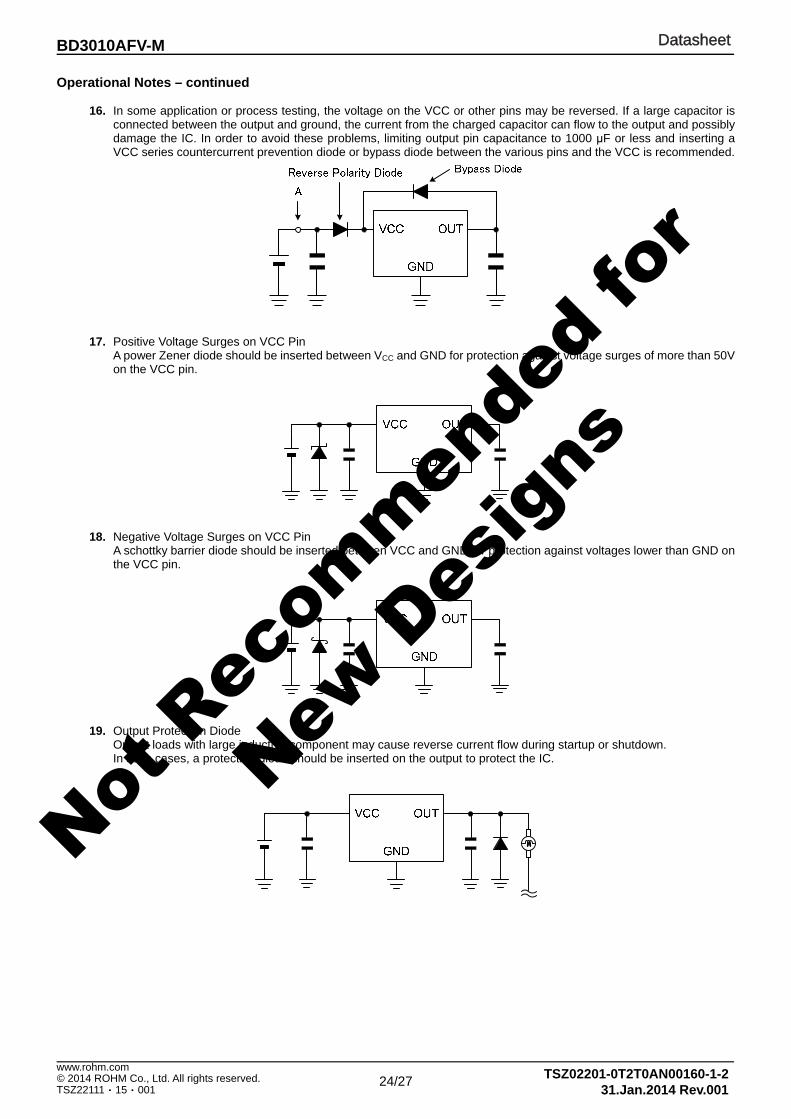
Operational Notes – continued
16. In some application or process testing, the voltage on the VCC or other pins may be reversed. If a large capacitor is connected between the output and ground, the current from the charged capacitor can flow to the output and possibly damage the IC. In order to avoid these problems, limiting output pin capacitance to 1000 μF or less and inserting a VCC series countercurrent prevention diode or bypass diode between the various pins and the VCC is recommended.
17. Positive Voltage Surges on VCC Pin
A power Zener diode should be inserted between VCC and GND for protection against voltage surges of more than 50V on the VCC pin.
18. Negative Voltage Surges on VCC Pin
A schottky barrier diode should be inserted between VCC and GND for protection against voltages lower than GND on the VCC pin.
19. Output Protection Diode
Output loads with large inductive component may cause reverse current flow during startup or shutdown. In such cases, a protection diode should be inserted on the output to protect the IC.
Not R
ecom
men
ded
for
New D
esig
ns

BD3010AFV-M
25/27
DatasheetDatasheet
© 2014 ROHM Co., Ltd. All rights reserved. www.rohm.com
TSZ22111・15・001
TSZ02201-0T2T0AN00160-1-231.Jan.2014 Rev.001
Ordering Information
B D 3 0 1 0 A F V - M E 2
Part Number Package FV: SSOP-B20
Packaging and forming specification E2: Embossed tape and reel
Marking Diagram
SSOP-B20(TOP VIEW)
3 0 1 0 A F V
Part Number Marking
LOT Number
1PIN MARK
Not R
ecom
men
ded
for
New D
esig
ns

BD Datasheet
© 2ww
TSZ
P
D3010AFV Datasheet
2014 ROHM Coww.rohm.com
Z22111・15・0
Physical D
Package Na
V-M Datasheet
o., Ltd. All rights 001
Dimension,
ame
<T
Datasheet
reserved.
Tape and R
<Tape and Reel i
EmTape
Quantity
Direction of feed
Thre
250
E2
(
Re
Datasheet
Reel Informa
∗ Ord
l information>
mbossed carrier tap
The direction is the 1reel on the left hand
500pcs
2
Reel1pin
26/27
Datasheet
ation
SS
rder quantity needs to
tape
e 1pin of product is atd and you pull out th
in
Datasheet
SOP-B20
to be multiple of the m
at the upper left whe the tape on the right
Direction
Datasheet
TSZ0
minimum quantity.
hen you hold ht hand )
on of feed
Datasheet
02201-0T2T031.Jan
DatasheDatasheet
0AN00160-1.2014 Rev.00
eetDatasheet
-201
Not R
ecom
men
ded
for
New D
esig
ns

BD3010AFV-M
27/27
DatasheetDatasheet
© 2014 ROHM Co., Ltd. All rights reserved. www.rohm.com
TSZ22111・15・001
TSZ02201-0T2T0AN00160-1-231.Jan.2014 Rev.001
Revision History
Date Revision Changes
31.Jan.2014 001 New Release
Not R
ecom
men
ded
for
New D
esig
ns

DatasheetDatasheet
Notice - SS Rev.002© 2014 ROHM Co., Ltd. All rights reserved.
Notice Precaution on using ROHM Products
1. If you intend to use our Products in devices requiring extremely high reliability (such as medical equipment (Note 1), aircraft/spacecraft, nuclear power controllers, etc.) and whose malfunction or failure may cause loss of human life, bodily injury or serious damage to property (“Specific Applications”), please consult with the ROHM sales representative in advance. Unless otherwise agreed in writing by ROHM in advance, ROHM shall not be in any way responsible or liable for any damages, expenses or losses incurred by you or third parties arising from the use of any ROHM’s Products for Specific Applications.
(Note1) Medical Equipment Classification of the Specific Applications JAPAN USA EU CHINA
CLASSⅢ CLASSⅢ
CLASSⅡb CLASSⅢ
CLASSⅣ CLASSⅢ
2. ROHM designs and manufactures its Products subject to strict quality control system. However, semiconductor
products can fail or malfunction at a certain rate. Please be sure to implement, at your own responsibilities, adequate safety measures including but not limited to fail-safe design against the physical injury, damage to any property, which a failure or malfunction of our Products may cause. The following are examples of safety measures:
[a] Installation of protection circuits or other protective devices to improve system safety [b] Installation of redundant circuits to reduce the impact of single or multiple circuit failure
3. Our Products are not designed under any special or extraordinary environments or conditions, as exemplified below. Accordingly, ROHM shall not be in any way responsible or liable for any damages, expenses or losses arising from the use of any ROHM’s Products under any special or extraordinary environments or conditions. If you intend to use our Products under any special or extraordinary environments or conditions (as exemplified below), your independent verification and confirmation of product performance, reliability, etc, prior to use, must be necessary:
[a] Use of our Products in any types of liquid, including water, oils, chemicals, and organic solvents [b] Use of our Products outdoors or in places where the Products are exposed to direct sunlight or dust [c] Use of our Products in places where the Products are exposed to sea wind or corrosive gases, including Cl2,
H2S, NH3, SO2, and NO2
[d] Use of our Products in places where the Products are exposed to static electricity or electromagnetic waves [e] Use of our Products in proximity to heat-producing components, plastic cords, or other flammable items [f] Sealing or coating our Products with resin or other coating materials [g] Use of our Products without cleaning residue of flux (even if you use no-clean type fluxes, cleaning residue of
flux is recommended); or Washing our Products by using water or water-soluble cleaning agents for cleaning residue after soldering
[h] Use of the Products in places subject to dew condensation
4. The Products are not subject to radiation-proof design. 5. Please verify and confirm characteristics of the final or mounted products in using the Products. 6. In particular, if a transient load (a large amount of load applied in a short period of time, such as pulse. is applied,
confirmation of performance characteristics after on-board mounting is strongly recommended. Avoid applying power exceeding normal rated power; exceeding the power rating under steady-state loading condition may negatively affect product performance and reliability.
7. De-rate Power Dissipation (Pd) depending on Ambient temperature (Ta). When used in sealed area, confirm the actual
ambient temperature. 8. Confirm that operation temperature is within the specified range described in the product specification. 9. ROHM shall not be in any way responsible or liable for failure induced under deviant condition from what is defined in
this document.
Precaution for Mounting / Circuit board design 1. When a highly active halogenous (chlorine, bromine, etc.) flux is used, the residue of flux may negatively affect product
performance and reliability. 2. In principle, the reflow soldering method must be used; if flow soldering method is preferred, please consult with the
ROHM representative in advance. For details, please refer to ROHM Mounting specification
Not R
ecom
men
ded
for
New D
esig
ns

DatasheetDatasheet
Notice - SS Rev.002© 2014 ROHM Co., Ltd. All rights reserved.
Precautions Regarding Application Examples and External Circuits 1. If change is made to the constant of an external circuit, please allow a sufficient margin considering variations of the
characteristics of the Products and external components, including transient characteristics, as well as static characteristics.
2. You agree that application notes, reference designs, and associated data and information contained in this document
are presented only as guidance for Products use. Therefore, in case you use such information, you are solely responsible for it and you must exercise your own independent verification and judgment in the use of such information contained in this document. ROHM shall not be in any way responsible or liable for any damages, expenses or losses incurred by you or third parties arising from the use of such information.
Precaution for Electrostatic
This Product is electrostatic sensitive product, which may be damaged due to electrostatic discharge. Please take proper caution in your manufacturing process and storage so that voltage exceeding the Products maximum rating will not be applied to Products. Please take special care under dry condition (e.g. Grounding of human body / equipment / solder iron, isolation from charged objects, setting of Ionizer, friction prevention and temperature / humidity control).
Precaution for Storage / Transportation 1. Product performance and soldered connections may deteriorate if the Products are stored in the places where:
[a] the Products are exposed to sea winds or corrosive gases, including Cl2, H2S, NH3, SO2, and NO2 [b] the temperature or humidity exceeds those recommended by ROHM [c] the Products are exposed to direct sunshine or condensation [d] the Products are exposed to high Electrostatic
2. Even under ROHM recommended storage condition, solderability of products out of recommended storage time period may be degraded. It is strongly recommended to confirm solderability before using Products of which storage time is exceeding the recommended storage time period.
3. Store / transport cartons in the correct direction, which is indicated on a carton with a symbol. Otherwise bent leads
may occur due to excessive stress applied when dropping of a carton. 4. Use Products within the specified time after opening a humidity barrier bag. Baking is required before using Products of
which storage time is exceeding the recommended storage time period.
Precaution for Product Label QR code printed on ROHM Products label is for ROHM’s internal use only.
Precaution for Disposition When disposing Products please dispose them properly using an authorized industry waste company.
Precaution for Foreign Exchange and Foreign Trade act Since our Products might fall under controlled goods prescribed by the applicable foreign exchange and foreign trade act, please consult with ROHM representative in case of export.
Precaution Regarding Intellectual Property Rights 1. All information and data including but not limited to application example contained in this document is for reference
only. ROHM does not warrant that foregoing information or data will not infringe any intellectual property rights or any other rights of any third party regarding such information or data. ROHM shall not be in any way responsible or liable for infringement of any intellectual property rights or other damages arising from use of such information or data.:
2. No license, expressly or implied, is granted hereby under any intellectual property rights or other rights of ROHM or any
third parties with respect to the information contained in this document.
Other Precaution 1. This document may not be reprinted or reproduced, in whole or in part, without prior written consent of ROHM. 2. The Products may not be disassembled, converted, modified, reproduced or otherwise changed without prior written
consent of ROHM. 3. In no event shall you use in any way whatsoever the Products and the related technical information contained in the
Products or this document for any military purposes, including but not limited to, the development of mass-destruction weapons.
4. The proper names of companies or products described in this document are trademarks or registered trademarks of
ROHM, its affiliated companies or third parties.
Not R
ecom
men
ded
for
New D
esig
ns

DatasheetDatasheet
Notice – WE Rev.001© 2014 ROHM Co., Ltd. All rights reserved.
General Precaution 1. Before you use our Pro ducts, you are requested to care fully read this document and fully understand its contents.
ROHM shall n ot be in an y way responsible or liabl e for fa ilure, malfunction or acci dent arising from the use of a ny ROHM’s Products against warning, caution or note contained in this document.
2. All information contained in this docume nt is current as of the issuing date and subj ect to change without any prior
notice. Before purchasing or using ROHM’s Products, please confirm the la test information with a ROHM sale s representative.
3. The information contained in this doc ument is provi ded on an “as is” basis and ROHM does not warrant that all
information contained in this document is accurate an d/or error-free. ROHM shall not be in an y way responsible or liable for any damages, expenses or losses incurred by you or third parties resulting from inaccuracy or errors of or concerning such information.
Not R
ecom
men
ded
for
New D
esig
ns