2-c z? '9 - NASA · · 2017-06-26Capacitance and Current versus Voltage for a Varactor Diode ......
27
' I N 0 ITHRUI (ACCESSION NUMFERl f GPO PRICE $ CFSTI PRICE(S) $ Hard copy (HC) 2-c z? Microfiche (M F) '9 ff 653 July65 MICROWAVE C ORPORAT ION w 1 7 A SUBSIDIARY OF MELPAR, INC. 420 KIRBY STREET GARLAND, TEXAS https://ntrs.nasa.gov/search.jsp?R=19660004061 2018-07-01T00:57:35+00:00Z
Transcript of 2-c z? '9 - NASA · · 2017-06-26Capacitance and Current versus Voltage for a Varactor Diode ......
'I
N 0
ITHRUI (ACCESSION NUMFERl f
GPO PRICE $
CFSTI PRICE(S) $
Hard copy (HC) 2 - c z? Microfiche (M F) '9
ff 653 July65
MICROWAVE C ORPORAT I O N w 1
7
A S U B S I D I A R Y OF M E L P A R , INC. 420 K I R B Y S T R E E T G A R L A N D , T E X A S
https://ntrs.nasa.gov/search.jsp?R=19660004061 2018-07-01T00:57:35+00:00Z

F I N A L REPORT
THE DEVELOPMENT OF AN S-BAND PARAMETRIC A M P L I F I E R U S I N G NEW
TECHNIQUES FOR GAIN S T A B I L I Z A T I O N
SUBMITTED NOVEMBER 1965
ON
CONTRACT NAS8 - 118 17
WITH
NATIONAL AERONAUTICS AND SPACE ADMINISTRATION
GEORGE C. MARSHALL SPACE
F L I G H T CENTER
M I C R O W A V E P H Y S I C s C O R P O R A T I O N
420 K i r b y Street G a r l and , Texas

TABLE OF CONTENTS
Summary
P r o j e c t Ob jec t ive
Technica l Discussion
Genera 1
Design Cons idera t ions
Amplifier Equivalent C i r c u i t and Gain Formula
Gain Compensation by Automatic Adjustment of Voltage Operating Po in t
Temperature Compensation
Laboratory Model
R e 1 i a b i 1 i t y
Resu l t s o f t he Study
Bib 1 iography
1.
2 .
3 .
4 .
5 .
6 .
7 .
8.
9 .
10.
11.
12.
LIST OF ILLUSTRATIONS
Sys t e m Block Diagram
C i r c u i t Model fo r t h e Negative Res is tance Paramet r ic Amplifier ope ra t ed wi th a C i r c u l a t o r
Capacitance and Current versus Voltage f o r a Varactor Diode
S i m p l i f i e d Schematic of Varactor Se l f -B ias ing Arrangement
At t enua t ion (vs) Temperature
At t enua t ion (vs) Bias
Bias (vs) Teruperature
Schematic of Bias Supply
Ampl i f ie r Gain (vs ) Temperature
Frequency Change (vs) T e m p e r a t u r e
Schematic Diagram - S-Band Parametric Amplifier
Photograph c?f S-Band Parametric Amplifier
Page No. i
2
4
4
5
5
1 :1
r j
'7

SUMMARY / 3 3 6
This r e p o r t desc r ibes t h e r e s u l t s o f a r e sea rch and development program
i n v e s t i g a t i n g parametr ic ampl i f i e r ga in s t a b i l i z a t i o n us ing temperature
sens ing and compensation techniques. The work included development,
t e s t i n g , and d e l i v e r y of an opera t ing l abora to ry model of an S-band
a m p l i f i e r tuned t o 2.276 Gc. This ampl i f i e r should have a wide v a r i e t y
of a p p l i c a t i o n s i n communications o r t r a c k i n g systems i n which tempera-
t u r e changes are sensed and cor rec ted f o r , thus e l imina t ing t h e r e q u i r e -
ment f o r a c o n t r o l l e d environment.
1
PROJECT OBJECTIVE
The work undertaken on t h i s c o n t r a c t w a s d i r e c t e d t o develop
techniques f o r ga in s t a b i l i z a t i o n of an S-band paramet r ic a m p l i f i e r
by temperature sens ing and compensation.
Design goa ls included e l imina t ing the requirement f o r a c a r e f u l l y
c o n t r o l l e d environment and minimizing o p e r a t i o n a l warm-up time
and power requi rements . High system r e l i a b i l i t y and e l imina t ion
of manual adjustments f o r normal ampl i f i e r performance were p r a c t i c a l
o b j e c t i v e s f o r t h e d e l i v e r a b l e l abora to ry model. E f f o r t s were
expected t o r e s u l t i n an a m p l i f i e r which w i l l have a wide a p p l i c a t i o n
i n a v a r i e t y of communication o r t rack ing systems r e q u i r i n g minimum
maintenance and s i m p l i f i e d opera t ion .
The l a b o r a t o r y model S-band parametric a m p l i f i e r w a s t o meet t h e
f o l lowing spec i f ica t ions :
a . General:
Center frequency Bandwidth
Noise f igure--maximum Gain Gain Var ia t ion- -des ign goa l
--maximum Spurious response r e j e c t i o n
--design goa 1 Intermodu la t ion r e j e c t ion (a l l
o r d e r s ) --des ign goa 1
2276.424 Gc. As determined by phase res pons e requirements 2 dB 17 dB + 0.5 dB z 1.5 dB
80 dB 80 dB 80 dB
2

E
b
-30' C t o +75O C Operating temperature range Phase Response
D i f f e r e n t i a l Phase S h i f t between 5wo s i g n a l s 3.2 Gc apar t , t h a t may encounter Doppler frequency s h i f t s of 8 0- -maximum 2 00
D i f f e r e n t i a 1 phase va r i a t ion over 3 .2 Gc bandwidthdue t o a l l sources--design goa l lo
Phase l i n e a r i t y over 3 . 2 Gc bandwidth--design goal lo
Pump power leakage Warm-up time Primary power
-20 dB 2 seconds 110/220 V + - lo%, 60 cps
The a m p l i f i e r s h a l l n o t limit on n o i s e , bu t s h a l l be a b l e t o wi ths tand
a n input s i g n a l l e v e l of -65 dBm wi thout s e r i o u s degrada t ion in
performance
C . The ampl i f i e r s h a l l no t r equ i r e manual tuning o r adjustment t o remain
w i t h i n s p e c i f i e d l i m i t s .
The ampl i f i e r s h a l l be packaged i n a s tandard 19-inch rack mounting.
Appropriate ou tputs f o r monitoring and record ing a m p l i f i e r performance
s h a l l be provided, inc luding pump power, e t c .
The a m p l i f i e r s h a l l have a c e r t i f i e d 98 percent p r o b a b i l i t y of normal
ope ra t ion over a per iod of two yea r s , inc luding on-off cyc l ing , wi th-
o u t degradat ion of performance o u t s i d e the s p e c i f i e d l i m i t s .
d .
e .
f .
3

C
TECHNICAL DISCUSS ION
GENERAL.
a m p l i f i e r . Among these w a s t he e l imina t ion of a v a r a c t o r diode b i a s
source through t h e use of s e l f - b i a s and open loop temperature sens ing
and c o n t r o l . Before d i scuss ing these techniques i n d e t a i l , s e v e r a l
o t h e r fea tures o f t h e design w i l l be descr ibed and t h e i r e f f e c t on t h e
ope ra t ion d iscussed .
Severa l new techniques were employed i n the des ign of t he
A f i v e - p o r t low l o s s c i r c u l a t o r was employed t o g ive g r e a t e r than 40 dB
of i s o l a t i o n o n , b o t h the inpu t and output p o r t s of t h e a m p l i f i e r . This
n o t on ly improved inpu t and output te rmina t ion VSWR bu t gave s u f f i c i e n t
i s o l a t i o n of t he a m p l i f i e r from ex te rna l connect ions t o eliminate causes
of ga in v a r i a t i o n which might be present due t o e x t e r n a l VSWR.
The a m p l i f i e r system w a s constructed wi th as many s o l i d s t a t e components
as was f e a s i b l e t o provide t h e h ighes t r e l i a b i l i t y . The pump source
was powered by a s i l i c o n d-c power supply wi th s u f f i c i e n t load and l i n e
r e g u l a t i o n t o e l i m i n a t e ga in v a r i a t i o n s due t o e x t e r n a l power f l u c t u a t i o n s .
The a m p l i f i e r w a s designed t o be con t ro l l ed wi th a minimum number of
mechanical o r e l e c t r i c a l adjustments and i s f r e e of tun ing once t h e des i red
frequency and ga in are se t .
by t h e use of a f ixed-frequency s o l i d s t a t e source . S i g n a l frequency
i s a d j u s t e d by va rac to r diode b ias adjustments and t h e ga in i s c o n t r o l l e d
by t h e amount of pump power supplied t o the va rac to r mount. The vi i ractor
mount w a s designed t o provide the s i m p l i f i e d c o n t r o l s u s ing convent iona l
techniques and w i l l no t be discussed he re , bu t it should be poin ted ou t
Pump frequency adjustments a re e l imina ted
4
t h a t i t w a s necessary t o achieve the s i m p l i f i e d c o n t r o l ope ra t ion
before i n v e s t i g a t i n g gain s t a b i l i z a t i o n techniques . E s s e n t i a l l y , i t w a s
necessary t o have s i m p l i f i e d con t ro l so t h a t once v a r i a t i o n s are sensed
t h e r e would be an easy way t o r ea l ign t h e a m p l i f i e r and achieve ga in
s t a b i l i z a t i o n .
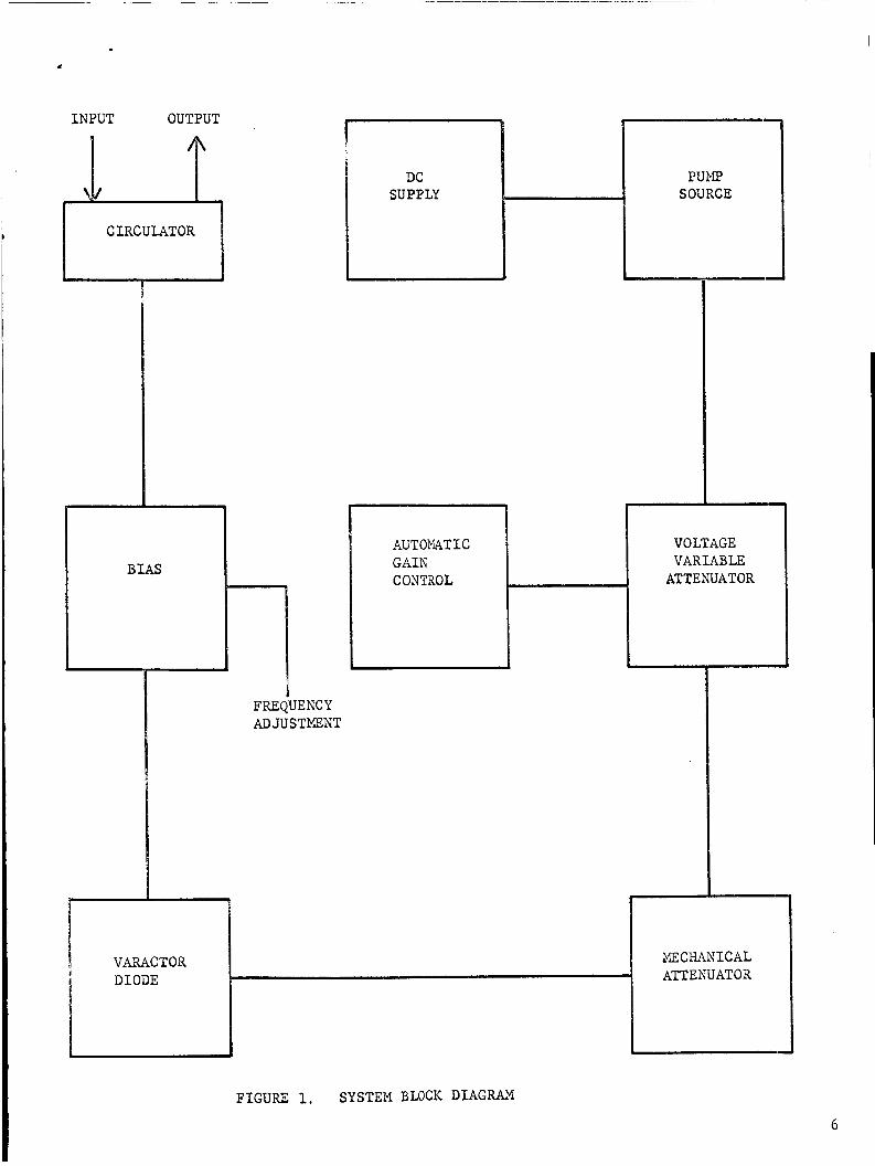
A f u n c t i o n a l block diagram, f i g u r e 1, i d e n t i f i e s t h e major components
of t h e a m p l i f i e r system.
D E S I G N CONSIDERATIONS.
are negat ive r e s i s t a n c e a m p l i f i e r s which r e q u i r e a cons tan t d i f f e r e n c e
between e x t e r n a l and in ' -e rna l r e s i s t a n c e t o main ta in s t a b l e ga in .
t i o n i n ambient temperature w i l l cause t h e i n t e r n a l nega t ive r e s i s t a n c e
t o change. This change i n i n t e r c a l r e s i s t a n c e can be r e l a t e d t o changes
i n i n d i v i d u a l parameters which make i'i up from an examination of t h e
a m p l i f i e r ga in express ion . 1: i s the purpose of t h i s d i scuss ion t o show
t h e e f f e c t on ga in of changes i n pump power l e v e l and va rac to r diode s e r i e s
r e s i s t a n c e . These two f a c t o r s a r e normally g r e a t l y a f f e c t e d by change i n
temperature .
Nondegenerate v a r a c t o r diode parametric a m p l i f i e r s
Varia-
AMPLIFIER EQUIVALENT CIRCUIT L7.D G A I N FO€CWLA. The a m p l i f i e r equ iva len t
c i r c u i t and ga in formula used here a re taken from Blackwell and Xotzebue . The equ iva len t c i r c u i t f o r t he ampl i f i e r w i t h a f e r r i t e c i r c u l a t o r i s
shown i n f i g u r e 2 . The power gain f o r t h e a m p l i f i e r is:
1
2 2 G = 4 Rg /(I$,l -R)
where :
t
5
I N P U T OUTPUT
w CIRCULATOR
BIAS
1 !
I FREQUENCY ADJUSTMENT
DC 1 SUPPLY PUMP SOURCE
VOLTAGE VARIABLE
ATTENUATOR
MECHANICAL ATTENUATOR
1 F I G U R E 1. SYSTEM BLOCK DIAGRAM
6

R = genera tor r e s i s t a n c e = g
Zo of input l i n e connecting t o v a r a c t o r diode
R = R + Rs; Rs = series r e s i s t a n c e of t h e v a r a c t o r diode T 1 g
2 -v -R = - w w CZRs
1 2
y = AC/2Co, the normalized capaci tance v a r i a t i o n r e s u l t i n g from applying pump vol tage
Co = j unc t ion capac i tance of the v a r a c t o r diode a t ope ra t ing
p o i n t
w = s i g n a l angular frequency
w = i d l e r angular frequency 1
2
I n o rde r t o examine t h e e f f e c t of normally v a r i a b l e f a c t o r s on ga in ,
Equat ion (1) may be w r i t t e n as follows:
2 4 R
2 G =
r R + R - ,.
By us ing a c i r c u l a t o r a t t h e ampl i f i e r input t o i s o l a t e t h e e f f e c t of
v a r i a b l e e x t e r n a l impedances such as might be caused by a r o t a t i n g
an tenna , R
connect ing t o the diode. This impedance, and thus R , w i l l vary only
s l i g h t l y , i f a t a l l , over a ve rywide range of temperature and can be con-
becomes t h e c h a r a c t e r i s t i c impedance of t he coax ia l l i n e g
g
s i d e r e d t o be cons t an t i n t h e p r a c t i c a l ca se . The f requencies r ep resen ted
by w1 and w2 are p r a c t i c a l l y cocs tsn t a l s o , e s p e c i a l l y i f t h e pump source
is c o n t r o l l e d i n frequency a s wou ld be t h e case f o r a s o l i d s ta te source .
The diode capac i tance , C y i s temperature s e n s i t i v e ; however, t he e f f e c t is
0 rc,
0 N
0 LJ
' 0 > 9 -
I
in I -
k 0 I
i U W (d k I cd > I
k o c u-co
o p . 3 a
c u c d c .rl ~
m a J . k 7 bo
.rl Fr
9
a s l i g h t detuning of t h e a m p l i f i e r center frequency which i s no t t roub le -
some f o r an a m p l i f i e r design of s u f f i c i e n t bandwidth,
f a c t o r s are y and Rs, each of which is s e n s i t i v e t o changes i n t empera -
t u r e . The f a c t o r y is a i f e c t e d by teinperature i n d i r e c t l y as a r e s u l t
of pump power l e v e l being v a r i h j l e with temperature .
The remaining
A t t h i s po in t , a design example should be examined i n o rde r t o determine
the magnitude of t h e e f f e c t s of v a r i a t i o n i n y and R . It can be shown
t h e o r e t i c a l l y and from p r a c t i c a l design examples t h a t a n o i s e f i g u r e l e s s
S
than 2.G a B can be obta ined a t 2300 G c w i t h commercially a v a i l a b l e v a r a c t o r
diodes pumped a t 13,500 Gc. S u f f i c i e n t bandwidth can a l s o be obta ined;
cherefore , t he fol iowing d iscuss ion w i l l apply t o ob ta in ing the r equ i r ed
ga in i n t h e a m p l i f i e r .
CHARACTERISTIC PARAMETERS FOR VARACTOR DIODE PARAMETRIC AMPLIFIER
f s = f , = 2,300 Gc
f p = 13,500 GC
f i = f 2 = 11,200 GC
C a t -0 .5 vo l t s = 0.5 Pf
Rs = 2.50 ohms a t 25' C
y = a C / 2 C 0 = 0.13
Rg = 30 ohms
S u b s t i t u t i o n of t h e ~ a b o v e values i n t o equat ion 2 r e s u l t s i n a c a l c u l a t e d
g a i n of 17.35 dB.
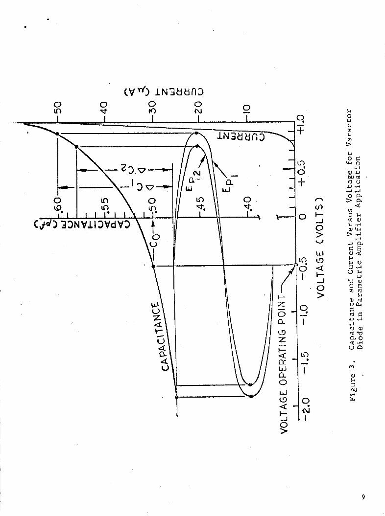
p o i n t f o r t h i s a m p l i f i e r a r e snown i n f i g u r e 3 .
show capac i tance versus vol tage and c u r r e n t versus v o l t a g e f o r a t y p i c a l
ga l l i um a r sen ide v a r a c t o r diode,
The opera t ing average capac i tance and b i a s vo l t age
The curves of f i g u r e 3
The r e l a t i o n s h i p of y (y =AC/2C,) t o

. t h e magnitude of t he pump vo l t age may be seen g r a p h i c a l l y from t h i s
curve . For t h e a m p l i f i e r example worked o u t above, t h e pump
vo l t age r equ i r ed t o o b t a i n y = 0.13 is 2.9 v o l t s peak-to-peak wi th t h e
ope ra t ing vo l t age po in t s e t a t -0 .5 v o l t w i t h a s e p a r a t e b i a s i n g source
such as a b a t t e r y .
y from 0.13 t o y = 0.12.
t o 14.75 dB. S imi l a r ly , t h e e f f e c t of an inc rease i n pump vo l t age can
be determined. A t l e a s t 10 percent change i n pump vo l t age , about 0.4 dB,
can be expected from most uncompensated pump sources a v a i l a b l e over t he
temperature range from -30 t o +60° C .
A r educ t ion i n pump vo l t age of 10 pe rcen t would change
The gain would change from a va lue of 17.35 dB
GAIN COMPENSATION BY AUTOMATIC ADJUSTMENT OF VOLTAGE OPERATING POINT,
The preceding d i scuss ion has shown t h a t a decrease i n y caused by a
decrease i n pump vo l t age w i l l produce a correspondingly l a r g e decrease i n
a m p l i f i e r ga in . This occurs because the ope ra t ing p o i n t i s f i x e d a t -0.5
v o l t s . I f t he ope ra t ing p o i n t were s h i f t e d t o a lower nega t ive vo l t age , y
would remain very close to i t s value p r i o r t o pump vo l t age decrease because
of t h e h igh degree of n o n l i n e a r i t y i n t h e capac i tance curve i n t h e range
from 0.7 t o 1 .0 v o l t s . From f igu re 3 , i t may be seen t h a t a s h i f t i n
t h e ope ra t ing p o i n t t o -0.36 v o l t from t h e o r i g i n a l -0.5 v o l t po in t would
almost e x a c t l y compensate f o r t h e drop i n peak pump vo l t age froia 1 .40 vo1t.s
t o 1.26 v o l t s .
than 0.500 p f .
of 9 Mc i n a m p l i f i e r cen ter frequency; however, t h e ampl i f i e r can be
designed wi th s u f f i c i e n t bandwidth t o maintain ga in a t t h e des ign c e n t e r
f requency.
A t t h e new opera t ing Doint, Co would be 0.505 r a t h e r
This change i n capaci tance w o ~ l d cause a c a l c u l a t e d change
The method of b i a s i n g t h e ampl i f ie r t o achieve an automatic s h i f t i n t h e
11
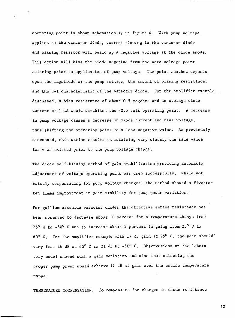
opera t ing p o i n t i s shown schematical ly i n f i g u r e 4 .
app l i ed t o t h e va rac to r diode, curren: f lowing i n t h e va rac to r diode
and b i a s ing r e s i s t o r w i l l b u i l d up a nega t ive vo l t age a t t he diode anode.
With pump vo l t age
This a c t i o n w i l l b i a s t he diode negat ive from t h e zero vo l t age po in t
e x i s t i n g p r i o r t o a p p l i c a t i o n of pump vo l t age . The po in t reached depends
upon t h e magnitude of t h e pump vol tage, t he amount of b i a s i n g r e s i s t a n c e ,
and t h e E-I c h a r a c t e r i s t i c o f t h e varac tor d iode . For t h e a m p l i f i e r example
d iscussed , a b i a s r e s i s t a n c e of about 0 .5 megohms and an average diode
c u r r e n t of 1 PA would e s t a b l i s h the -0 .5 v o l t ope ra t ing p o i n t .
i n pump vo l t age causes a decrease i n d iode cu r ren t and b i a s vo l t age ,
t hus s h i f t i n g t h e ope ra t ing p o i n t t o a less nega t ive va lue . As previous ly
d i scussed , t h i s a c t i o n r e s u l t s i n r e t a i n i n g very c l o s e l y t h e same va lue
f o r y as e x i s t e d p r i o r t o t h e pump vo l t age change.
A decrease
The d iode s e l f - b i a s i n g method of gain s t a b i l i z a t i o n providing automatic
adjustment of vo l t age ope ra t ing point w a s used s u c c e s s f u l l y . While n o t
e x a c t l y compensating f o r pump vol tage changes, t he method showed a f ive- t .0-
t e n t i m e s improvement i n ga in s t a b i l i t y f o r pump power v a r i a t i o n s .
For ga l l ium a r sen ide va rac to r diodes the e f f e c t i v e s e r i e s r e s i s t a n c e has
been observed t o decrease about 10 pe rcen t f o r a temperature change from
2 5 O C t o -30' C and t o inc rease about 3 percent i n going from 25' C t o
600 C.
v a r y from 16 dB a t 60° C t o 2 1 dB a t -30° C .
t o r y model showed such a ga in v a r i a t i o n and a l s o t h a t s e l e c t i n g t h e
proper pump power would achieve 17 dB of ga in over t h e e n t i r e temperature
range .
For t h e a m p l i f i e r example w i t h 1 7 dB ga in a t 25' C, t h e ga in should '
Observations on the labora-n
TEMPERATURE COMPENSATION. To compensate f o r changes i n diode r e s i s t a n c e
12
i cn t,
i P
! 1 I
cn i I s I
4-
aJ
13

.
and pump power v a r i a t i o n s not cor rec ted by the s e l f - b i a s arrangement, an
open loop temperature sensing and con t ro l l i ng c i r c u i t w a s employed. The
c i r c u i t used a vo l t age -va r i ab le a t t enua to r i n t h e pump l i n e t o vary the
power. A temperature-sensing device us ing the rmis to r s and diodes was
used t o supply a vary ing d r i v e vol tage t o t h e a t t e n u a t o r . This method w a s
used t o e l imina te t h e need fo r a cont ro l led system temperature such a s would be
provided by h e a t e r s and e l aborc t e box i n s u l a t i o n t o prevent diode and pump
changes. Fur ther , an open loop system w a s chosen t o e l imina te the need
f o r t h e pump power detection-and-feedback arrangement t h a t has been used
i n o the r systems. I n a c losed system t h e sampling dev ice would need t o
be temperature-compensated i t s e l f . To provide s i m p l i c i t y i n c o n t r o l c i r c u i t s ,
t he open method w a s used. F i r s t , data was taken on t h e amount of attenua.-
t i o n needed i n t h e pump l i n e t o maintain t h e a m p l i f i e r a t 1 7 dB of ga in
over t h e temperature range. Figure 6 shows t h e r e s u l t s . The vol tage-
v a r i a b l e a t t e n u a t o r u t i l i z e d a PIN semiconductor diode mounted i n a wave-.
guide s t r u c t u r e t o provide a va r i ab le lo s s wi th b i a s v o l t a g e . F igure 5
shows t y p i c a l a t t e n u a t i o n versus S ia s . The f i n a l s t e p i n t h e des ign
of t h e c o n t r o l c i r c u i t w a s t o bu i ld a b i a s supply t h a t would d r i v e t h e
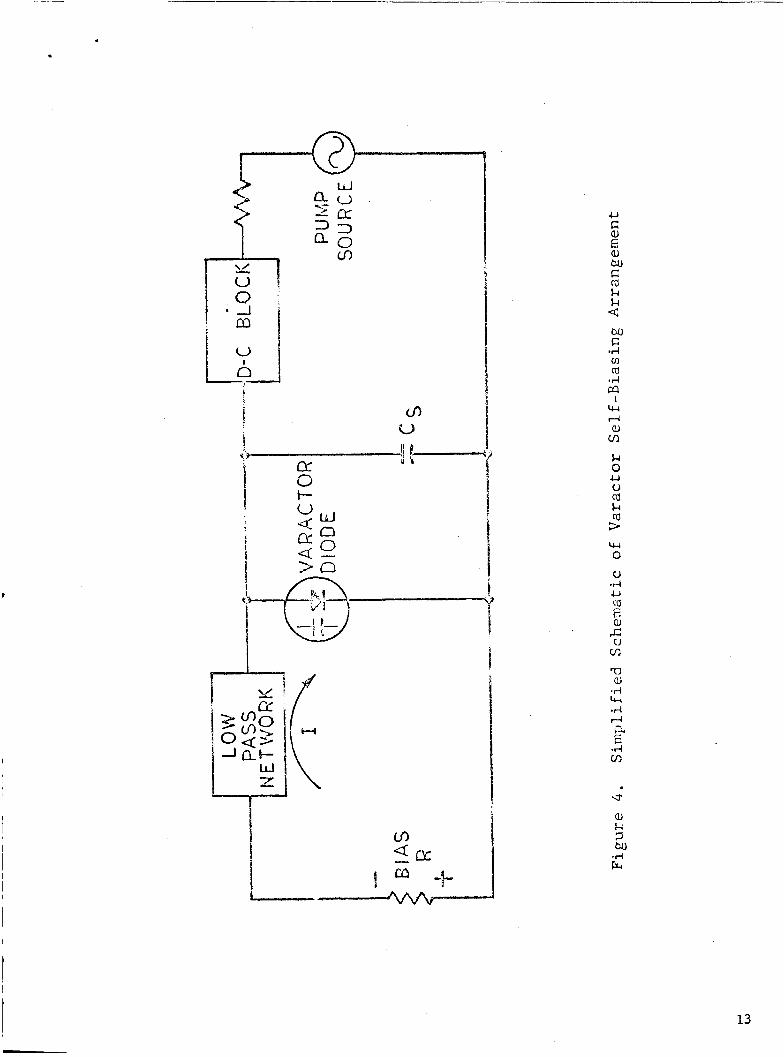
a t t e n u a t i o n i n t h e p re sc r ibed manner shown i n f i g u r e 7 .
were t r i e d us ing va r ious combinations of components. A d i f f e r e n t i a l
a m p l i f i e r arrangement proved too complicated and u n r e l i a b l e .
c i r c u i t shown i n f i g u r e 8 u t i l i z e d two diodes and a vo l t age d i v i d e r
network t o provide the needed output .
ments diminishing a t the high and low temperature extremes wi th a maximum
va lue a t room temperature .
h igh temperature by a decrease in pump power whi le t h e Rs of t h e diode
Severa l c i r c u i t s
The f i n a l
F igure 7 shows the b i a s r e q u i r e -
The s o l i d s t a t e source a f f e c t e d t h e curve a t

2 -
I -
- I
2v3 I I
400 AGC EiAS AA
FIG 5.
I I
600
I
1 1 I I I I I 1 I I I 1 -20 0 20 4 0 60 80
15
I I -20
I I 1 I I I I I I
0 2c 40 60 €10
TEMPERATURE "C FOG 7.
16

5.6 K ! R I
! i 0
1 7

e f f e c t e d the gain a t low tern;.s-ratures. The o v e r a l l ga in wi th AGC
compensation va r i ed +, 1.5 dB between -25O C and +55O C and s l i g h t l y
worse on the ends, This i s shown i n f i g u r e 10. The c e n t e r frequency
s h i f t is shown i n f i g u r e 9.
LABORATORY MODEL. The u n i t i s a g a i n - s t a b i l i z e d , non-degenerate para-
metric a m p l i f i e r , designed f o r low noise a m p l i f i c a t i o n a t 2.28 G c .
Automatic gain s t a b i l i z a t i o n i n an uncontrol led environment i s achieved
by means of a temperature seqs ing and compensation system. Any
temperature change t h a t would o r d i n a r i l y cause ga in v a r i a t i o n i s sensed
and a compensating vol tage is appl ied t o the PIN d iode i n a vo l t age -
v a r i a b l e a t t e n u a t o r t o c o n t r o l t h e output of t he s o l i d - s t a t e pump source .
The v a r a c t o r diode i s s e l f - b i a s e d to improve s t a b i l i t y and e l imina te the
need f o r a b i a s supply.
t h e ga in and cen te r frequency have been set , t he paramet r ic ampl i f i e r may
be opera ted unat tended. The parametric ampl i f i e r and a s s o c i a t e d waveguide
assemblies , a t t e n u a t o r s , c i r c u l a t o r s , d i r e c t i o n a l coupler , modular power
supply, modular pump source , AGC assembly, blower, and c o n t r o l pane l
are a l l contained i n a s i n g l e u n i t , packaged f o r r ack mounting. It should
be noted t h a t t h i s o p e r a t i o n a l conf igura t ion could be packaged as a much
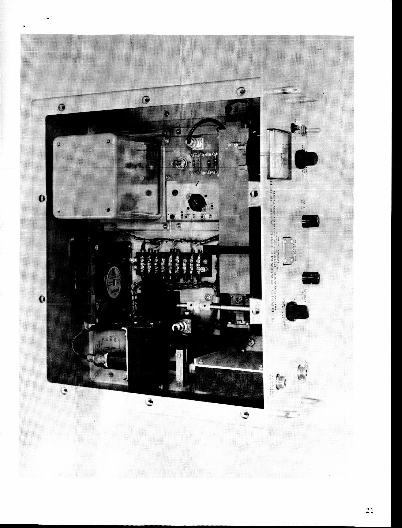
smaller u n i t . A system schematic i s shown i n f i g u r e 11. Figure 12 shows
Turn-on is e s s e n t i a l l y ins tan taneous and a f t e r
t h e e n t i r e u n i t and i t s components.
The u n i t exh ib i t ed the following e l e c t r i c a l c h a r a c t e r i s t i c s :
. ELECTRICAL CHARACTERISTICS
Power Input 110 vac, +, lo%, 60 cps
Center Frequency
Bandwidth 25 Mc, minimum (3 dB)
Noise Figure 2 dB, maximum
Gain 1 7 5 1.5 dB
2.28 Gc, +, 10 Mc
18

m 0
z W
C W LL J a E a
- a
- -
18
17
16
15
14
I I 1 I I I I i I I I I -20 0 20 40 60 80
TEMPERATURE OC
FIG 9.
1 I i I I I I I I I I - 20 0 20 40 60 €80 TEMPERATURE "C
FIG 10,
19

. . P R
N - r - E ; n o
-,mw 2 0 - U P
C 3 0. 3
.C 1 -.- " P " - >
l
t-
a 5 20
2 1
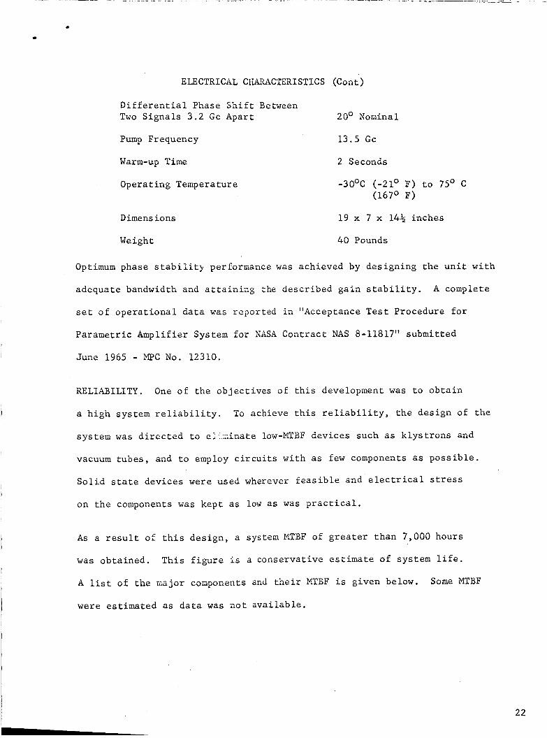
ELECTRICAL CH.AXACTERISTICS (Cont )
D i f f e r e n t i a l Phase S h i f t Between Two Signals 3.2 Gc A p a r t 20' Nominal
Pump Frequency 13.5 Gc
Warm-up T i m e
Operating Temperature
Dimens ions
2 Seconds
-3OOC (-21' F) t o 75' C (167O F)
19 x 7 x 14% inches
Weight 40 Pounds
Optimum phase s t a b i l i t y performance w a s achieved by designing the u n i t w i th
adequate bandwidth and a t t a i n i n g the descr ibed ga in s t a b i l i t y . A comp1et:e
s e t of o p e r a t i o n a l d a t a was repor ted i n "Acceptance Test Procedure f o r
Parametr ic Amplif ier System fo r NASA Contract NAS 8-11817" submit ted
June 1965 - MPC No. 12310.
RELIABILITY. One of t he ob jec t ives of t h i s development w a s t o o b t a i n
a h igh system r e l i a b i l i t y .
system w a s d i r e c t e d t o e;-:;:,inate low-MTBF devices such as k lys t rons and
To achieve t h i s r e l i a b i l i t y , t h e design of t he
vacuum tubes , and t o employ c i r c u i t s wi th as few components as p o s s i b l e .
S o l i d s t a t e devices were used wherever f e a s i b l e and e l e c t r i c a l s t ress
on t h e components w a s kept as low as w a s p r a c t i c a l .
A s a r e s u l t of t h i s des ign , a system MTBF of g r e a t e r than 7,000 hours
w a s ob ta ined . Th i s f i g u r e Ls a conserva t ive estimate of system l i f e .
A l i s t of t h e major components and t h e i r MTBF i s given below.
were es t imated as d a t a w a s n o t ava i l ab le .
Some MTBF
22
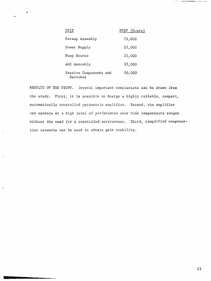
c
L
_L UNIT KTEF (Hours)
Paramp Assembly 75,000
Power Supply
Pump Source
AGC Assembly
25,000
25 , 000
35,000
Pass ive Components and 50,000 Switches
RESULTS OF THE STUDY. j e v e r a l important conclusions can be drawn from
the s tudy . F i r s t , i t i s p o s s i b l e t o des ign a h i g h l y r e l i a b l e , compact,
au tomat i ca l ly c o n t r o l l e d paramet r ic a m p l i f i e r . Second, t h e ampl i f i e r
can ope ra t e a t a high l e v e l of performance Over wide temperature ranges
wi thout t h e need f o r a c o n t r o l l e d environment. Thi rd , s i m p l i f i e d compensa-
t i o n networks can be used t o ob ta in ga in s t a b i l i t y .
23
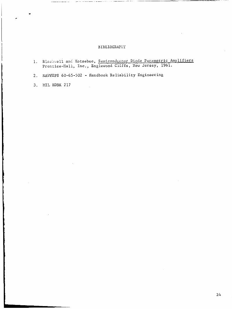
B I B L I O G R A P Z
1. Blzc;;:;sll anc: Kotzebue, Semiconductor Diode Paramet r ic Amplif iers Pren:ice-Hall, I n c . , Englewood C l i f f s , N e w J e r s e y , 1961.
2 . NAVWEPS 60-65-502 - Handbook R e l i a b i l i t y Engineering
3 . MIL HDBK 217
2 4