2-Bit, 2:1, Single-Ended Multiplexer 83052I-01
16
1 ©2015 Integrated Device Technology, Inc December 16, 2015 General Description The 83052I-01 is a 2-bit, 2:1, Single-ended Multiplexer and a member of the family of High Performance Clock Solutions from IDT. The 83052I-01 has two selectable single-ended clock inputs and two single-ended clock outputs. The output has a V DDO pin which may be set at 3.3V, 2.5V, or 1.8V, making the device ideal for use in voltage translation applications. An output enable pin places the output in a high impedance state which may be useful for testing or debug. Possible applications include systems with up to two transceivers which need to be independently set for different rates. For example, a board may have two transceivers, each of which need to be independently configured for 1 Gigabit Ethernet or 1 Gigabit Fibre Channel rates. Another possible application may require the ports to be independently set for FEC (Forward Error Correction) or non-FEC rates. The device operates up to 250MHz and is packaged in a 16 TSSOP. Features • 2-bit, 2:1 single-ended multiplexer • Nominal output impedance: 15 (V DDO = 3.3V) • Maximum output frequency: 250MHz • Propagation delay: 3ns (maximum), V DD = V DDO = 3.3V • Input skew: 85ps (maximum), V DD = V DDO = 3.3V • Part-to-part skew: 500ps (maximum), V DD = V DDO = 3.3V • Output skew: 65ps (maximum), V DD = V DDO = 3.3V • Additive phase jitter, RMS (12KHz - 20MHz): 0.15ps (typical) • Operating supply modes: V DD /V DDO 3.3V/3.3V 3.3V/2.5V 3.3V/1.8V 2.5V/2.5V 2.5V/1.8V • -40°C to 85°C ambient operating temperature • Available in lead-free (RoHS 6) package 83052I-01 16-Lead TSSOP 4.4mm x 5.0mm x 0.925mm package body G Package 1 2 3 4 5 6 7 8 16 15 14 13 12 11 10 9 VDD CLK1 SEL1 Q1 GND nc VDDO nc nc VDDO nc GND Q0 SEL0 CLK0 OE Pin Assignment 0 1 0 1 SEL0 CLK0 CLK1 SEL1 OE Q0 Q1 Pulldown Pulldown Pulldown Pulldown Pullup Block Diagram 83052I-01 Datasheet 2-Bit, 2:1, Single-Ended Multiplexer
Transcript of 2-Bit, 2:1, Single-Ended Multiplexer 83052I-01

1©2015 Integrated Device Technology, Inc December 16, 2015
General Description
The 83052I-01 is a 2-bit, 2:1, Single-ended Multiplexer and a member of the family of High Performance Clock Solutions from IDT. The 83052I-01 has two selectable single-ended clock inputs and two single-ended clock outputs. The output has a VDDO pin which may be set at 3.3V, 2.5V, or 1.8V, making the device ideal for use in voltage translation applications. An output enable pin places the output in a high impedance state which may be useful for testing or debug. Possible applications include systems with up to two transceivers which need to be independently set for different rates. For example, a board may have two transceivers, each of which need to be independently configured for 1 Gigabit Ethernet or 1 Gigabit Fibre Channel rates. Another possible application may require the ports to be independently set for FEC (Forward Error Correction) or non-FEC rates. The device operates up to 250MHz and is packaged in a 16 TSSOP.
Features
• 2-bit, 2:1 single-ended multiplexer
• Nominal output impedance: 15 (VDDO = 3.3V)
• Maximum output frequency: 250MHz
• Propagation delay: 3ns (maximum), VDD = VDDO = 3.3V
• Input skew: 85ps (maximum), VDD = VDDO = 3.3V
• Part-to-part skew: 500ps (maximum), VDD = VDDO = 3.3V
• Output skew: 65ps (maximum), VDD = VDDO = 3.3V
• Additive phase jitter, RMS (12KHz - 20MHz): 0.15ps (typical)
• Operating supply modes: VDD/VDDO
3.3V/3.3V3.3V/2.5V3.3V/1.8V2.5V/2.5V2.5V/1.8V
• -40°C to 85°C ambient operating temperature
• Available in lead-free (RoHS 6) package
83052I-01
16-Lead TSSOP4.4mm x 5.0mm x 0.925mm
package bodyG Package
12
345678
1615
1413121110
9VDD
CLK1SEL1
Q1GND
ncVDDO
nc ncVDDO
ncGNDQ0SEL0CLK0OE
Pin Assignment
0
1
0
1
SEL0
CLK0
CLK1
SEL1
OE
Q0
Q1
Pulldown
Pulldown
Pulldown
Pulldown
Pullup
Block Diagram
83052I-01Datasheet
2-Bit, 2:1, Single-Ended Multiplexer

2©2015 Integrated Device Technology, Inc December 16, 2015
83052I-01 Datasheet
Table 1. Pin Descriptions
NOTE: Pullup and Pulldown refer to internal input resistors. See Table 2, Pin Characteristics, for typical values.
Table 2. Pin Characteristics
Function TablesTable 3. Control Input Function Table
Number Name Type Description
1, 3, 14, 16 nc Unused No connect.
2, 15 VDDO Power Output supply pins.
4, 13 GND Power Power supply ground
5, 12 Q1, Q0 Output Single-ended clock outputs. LVCMOS/LVTTL interface levels.
6, 11 SEL1, SEL0 Input PulldownClock select inputs. See Table 3, Control Input Function Table. LVCMOS / LVTTL interface levels.
7, 10 CLK1, CLK0 Input Pulldown Single-ended clock input. LVCMOS/LVTTL interface levels.
8 VDD Power Power supply pin.
9 OE Input PullupOutput enable. When LOW, outputs are in HIGH impedance state. When HIGH, outputs are active. LVCMOS / LVTTL interface levels.
Symbol Parameter Test Conditions Minimum Typical Maximum Units
CIN Input Capacitance 4 pF
RPULLUP Input Pullup Resistor 51 k
RPULLDOWN Input Pulldown Resistor 51 k
CPDPower Dissipation Capacitance (per output); NOTE 1
VDDO = 3.465V 18 pF
VDDO = 2.625V 19 pF
VDDO = 2.0V 19 pF
ROUT Output Impedance
VDDO = 3.465V 15
VDDO = 2.625V 17
VDDO = 2.0V 25
Control Inputs Outputs
SEL1 SEL0 Q0 Q1
0 0 CLK0 (default) CLK0
0 1 CLK1 CLK0
1 0 CLK0 CLK1
1 1 CLK1 CLK1

3©2015 Integrated Device Technology, Inc December 16, 2015
83052I-01 Datasheet
Absolute Maximum RatingsNOTE: Stresses beyond those listed under Absolute Maximum Ratings may cause permanent damage to the device. These ratings are stress specifications only. Functional operation of product at these conditions or any conditions beyond those listed in the DC Characteristics or AC Characteristics is not implied. Exposure to absolute maximum rating conditions for extended periods may affect product reliability.
DC Electrical CharacteristicsTable 4A. Power Supply DC Characteristics, VDD = 3.3V ± 5%, VDDO = 3.3V ± 5% or 2.5V ± 5% or 1.8V ± 0.2V, TA = -40°C to 85°C
Table 4B. Power Supply DC Characteristics, VDD = 2.5V ± 5%, VDDO = 2.5V ± 5% or 1.8V ± 0.2V, TA = -40°C to 85°C
Item Rating
Supply Voltage, VCC 4.6V
Inputs, VI -0.5V to VDD + 0.5V
Outputs, VO -0.5V to VDDO+ 0.5V
Package Thermal Impedance, JA 100.3C/W (0 mps)
Storage Temperature, TSTG -65C to 150C
Symbol Parameter Test Conditions Minimum Typical Maximum Units
VDD Positive Supply Voltage 3.135 3.3 3.465 V
VDDO Output Supply Voltage
3.135 3.3 3.465 V
2.375 2.5 2.625 V
1.6 1.8 2.0 V
IDD Power Supply Current 40 mA
IDDO Output Supply Current No Load 5 mA
Symbol Parameter Test Conditions Minimum Typical Maximum Units
VDD Positive Supply Voltage 2.375 2.5 2.625 V
VDDO Output Supply Voltage2.375 2.5 2.625 V
1.6 1.8 2.0 V
IDD Power Supply Current 40 mA
IDDO Output Supply Current No Load 5 mA

4©2015 Integrated Device Technology, Inc December 16, 2015
83052I-01 Datasheet
Table 4C. LVCMOS/LVTTL DC Characteristics, TA = -40°C to 85°C
NOTE 1: Outputs terminated with 50 to VDDO/2. See Parameter Measurement Information, Output Load Test Circuit diagrams.
Symbol Parameter Test Conditions Minimum Typical Maximum Units
VIH Input High VoltageVDD = 3.465V 2 VDD + 0.3 V
VDD = 2.625V 1.7 VDD + 0.3 V
VIL Input Low VoltageVDD = 3.465V -0.3 1.3 V
VDD = 2.625V -0.3 0.7 V
IIHInput High Current
CLK0, CLK1, SEL0, SEL1VDD = VIN = 3.465V or
2.625V150 µA
OEVDD = VIN = 3.465V or
2.625V5 µA
IILInput Low Current
CLK0, CLK1, SEL0, SEL1VDD = 3.465V or 2.625V,
VIN = 0V-5 µA
OEVDD = 3.465V or 2.625V,
VIN = 0V-150 µA
VOH Output High Voltage; NOTE 1
VDDO = 3.3V ± 5% 2.6 V
VDDO = 2.5V ± 5% 1.8 V
VDDO = 1.8V ± 0.2V VDDO - 0.3 V
VOL Output Low Voltage; NOTE 1
VDDO = 3.3V ± 5% 0.5 V
VDDO = 2.5V ± 5% 0.45 V
VDDO = 1.8V ± 0.2V -5 0.35 V

5©2015 Integrated Device Technology, Inc December 16, 2015
83052I-01 Datasheet
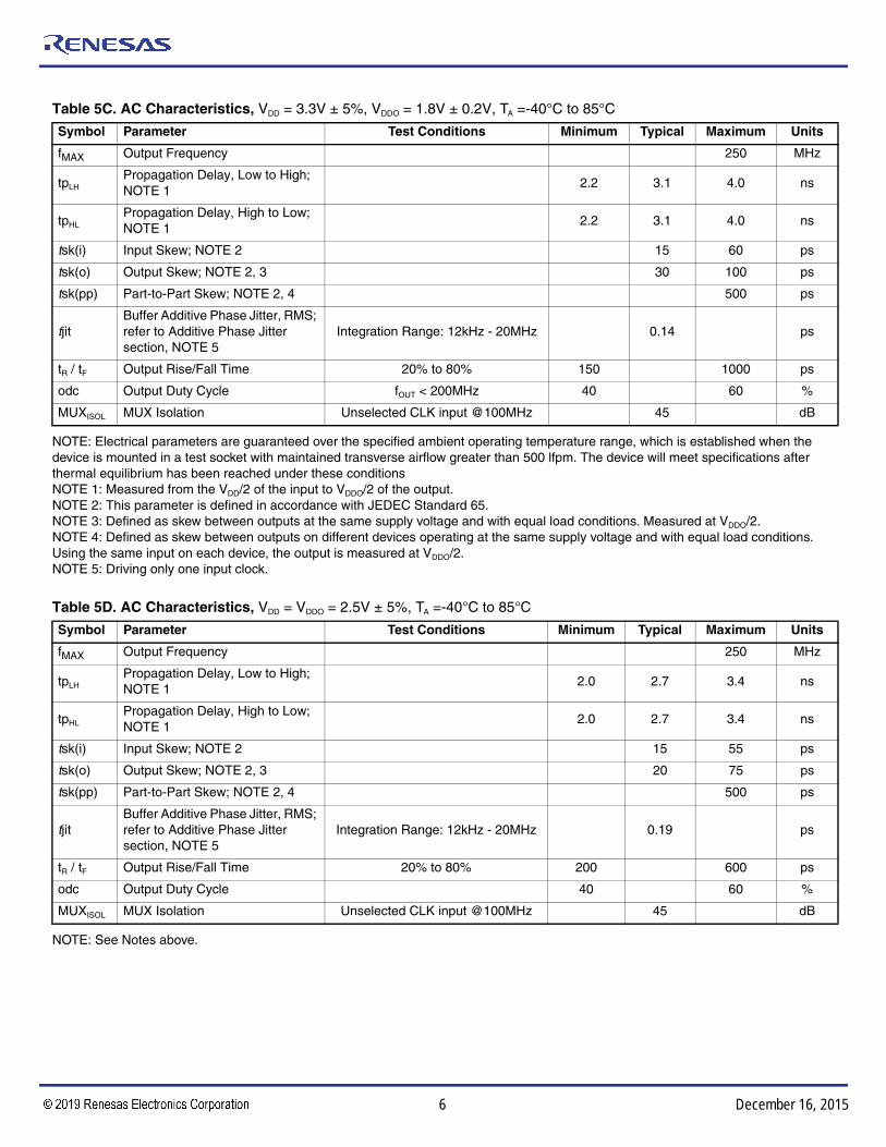
AC Electrical CharacteristicsTable 5A. AC Characteristics, VDD = VDDO = 3.3V ± 5%, TA =-40°C to 85°C
NOTE: Electrical parameters are guaranteed over the specified ambient operating temperature range, which is established when the device is mounted in a test socket with maintained transverse airflow greater than 500 lfpm. The device will meet specifications after thermal equilibrium has been reached under these conditionsNOTE 1: Measured from the VDD/2 of the input to VDDO/2 of the output.NOTE 2: This parameter is defined in accordance with JEDEC Standard 65.NOTE 3: Defined as skew between outputs at the same supply voltage and with equal load conditions. Measured at VDDO/2.NOTE 4: Defined as skew between outputs on different devices operating at the same supply voltage and with equal load conditions. Using the same input on each device, the output is measured at VDDO/2.NOTE 5: Driving only one input clock.
Table 5B. AC Characteristics, VDD = 3.3V ± 5%, VDDO = 2.5V ± 5%, TA =-40°C to 85°C
NOTE: See Notes above.
Symbol Parameter Test Conditions Minimum Typical Maximum Units
fMAX Output Frequency 250 MHz
tpLHPropagation Delay, Low to High; NOTE 1
2.0 2.45 3.0 ns
tpHLPropagation Delay, High to Low; NOTE 1
2.0 2.45 3.0 ns
tsk(i) Input Skew; NOTE 2 20 85 ps
tsk(o) Output Skew; NOTE 2, 3 15 65 ps
tsk(pp) Part-to-Part Skew; NOTE 2, 4 500 ps
tjitBuffer Additive Phase Jitter, RMS; refer to Additive Phase Jitter section, NOTE 5
Integration Range: 12kHz - 20MHz 0.15 ps
tR / tF Output Rise/Fall Time 20% to 80% 200 600 ps
odc Output Duty Cycle 40 60 %
MUXISOL MUX Isolation Unselected CLK input @100MHz 45 dB
Symbol Parameter Test Conditions Minimum Typical Maximum Units
fMAX Output Frequency 250 MHz
tpLHPropagation Delay, Low to High; NOTE 1
2.2 2.55 3.0 ns
tpHLPropagation Delay, High to Low; NOTE 1
2.2 2.55 3.0 ns
tsk(i) Input Skew; NOTE 2 10 50 ps
tsk(o) Output Skew; NOTE 2, 3 20 70 ps
tsk(pp) Part-to-Part Skew; NOTE 2, 4 500 ps
tjitBuffer Additive Phase Jitter, RMS; refer to Additive Phase Jitter section, NOTE 5
Integration Range: 12kHz - 20MHz 0.12 ps
tR / tF Output Rise/Fall Time 20% to 80% 200 600 ps
odc Output Duty Cycle 40 60 %
MUXISOL MUX Isolation Unselected CLK input @100MHz 45 dB
6©2015 Integrated Device Technology, Inc December 16, 2015
83052I-01 Datasheet
Table 5C. AC Characteristics, VDD = 3.3V ± 5%, VDDO = 1.8V ± 0.2V, TA =-40°C to 85°C
NOTE: Electrical parameters are guaranteed over the specified ambient operating temperature range, which is established when the device is mounted in a test socket with maintained transverse airflow greater than 500 lfpm. The device will meet specifications after thermal equilibrium has been reached under these conditionsNOTE 1: Measured from the VDD/2 of the input to VDDO/2 of the output.NOTE 2: This parameter is defined in accordance with JEDEC Standard 65.NOTE 3: Defined as skew between outputs at the same supply voltage and with equal load conditions. Measured at VDDO/2.NOTE 4: Defined as skew between outputs on different devices operating at the same supply voltage and with equal load conditions. Using the same input on each device, the output is measured at VDDO/2.NOTE 5: Driving only one input clock.
Table 5D. AC Characteristics, VDD = VDDO = 2.5V ± 5%, TA =-40°C to 85°C
NOTE: See Notes above.
Symbol Parameter Test Conditions Minimum Typical Maximum Units
fMAX Output Frequency 250 MHz
tpLHPropagation Delay, Low to High; NOTE 1
2.2 3.1 4.0 ns
tpHLPropagation Delay, High to Low; NOTE 1
2.2 3.1 4.0 ns
tsk(i) Input Skew; NOTE 2 15 60 ps
tsk(o) Output Skew; NOTE 2, 3 30 100 ps
tsk(pp) Part-to-Part Skew; NOTE 2, 4 500 ps
tjitBuffer Additive Phase Jitter, RMS; refer to Additive Phase Jitter section, NOTE 5
Integration Range: 12kHz - 20MHz 0.14 ps
tR / tF Output Rise/Fall Time 20% to 80% 150 1000 ps
odc Output Duty Cycle fOUT < 200MHz 40 60 %
MUXISOL MUX Isolation Unselected CLK input @100MHz 45 dB
Symbol Parameter Test Conditions Minimum Typical Maximum Units
fMAX Output Frequency 250 MHz
tpLHPropagation Delay, Low to High; NOTE 1
2.0 2.7 3.4 ns
tpHLPropagation Delay, High to Low; NOTE 1
2.0 2.7 3.4 ns
tsk(i) Input Skew; NOTE 2 15 55 ps
tsk(o) Output Skew; NOTE 2, 3 20 75 ps
tsk(pp) Part-to-Part Skew; NOTE 2, 4 500 ps
tjitBuffer Additive Phase Jitter, RMS; refer to Additive Phase Jitter section, NOTE 5
Integration Range: 12kHz - 20MHz 0.19 ps
tR / tF Output Rise/Fall Time 20% to 80% 200 600 ps
odc Output Duty Cycle 40 60 %
MUXISOL MUX Isolation Unselected CLK input @100MHz 45 dB

7©2015 Integrated Device Technology, Inc December 16, 2015
83052I-01 Datasheet
Table 5E. AC Characteristics, VDD = 2.5V ± 5%, VDDO = 1.8V ± 0.2V, TA =-40°C to 85°C
NOTE: Electrical parameters are guaranteed over the specified ambient operating temperature range, which is established when the device is mounted in a test socket with maintained transverse airflow greater than 500 lfpm. The device will meet specifications after thermal equilibrium has been reached under these conditionsNOTE 1: Measured from the VDD/2 of the input to VDDO/2 of the output.NOTE 2: This parameter is defined in accordance with JEDEC Standard 65.NOTE 3: Defined as skew between outputs at the same supply voltage and with equal load conditions. Measured at VDDO/2.NOTE 4: Defined as skew between outputs on different devices operating at the same supply voltage and with equal load conditions. Using the same input on each device, the output is measured at VDDO/2.NOTE 5: Driving only one input clock.
Symbol Parameter Test Conditions Minimum Typical Maximum Units
fMAX Output Frequency 250 MHz
tpLHPropagation Delay, Low to High; NOTE 1
2.0 3.1 4.2 ns
tpHLPropagation Delay, High to Low; NOTE 1
2.0 3.1 4.2 ns
tsk(i) Input Skew; NOTE 2 30 135 ps
tsk(o) Output Skew; NOTE 2, 3 30 95 ps
tsk(pp) Part-to-Part Skew; NOTE 2, 4 500 ps
tjitBuffer Additive Phase Jitter, RMS; refer to Additive Phase Jitter section, NOTE 5
Integration Range: 12kHz - 20MHz 0.17 ps
tR / tF Output Rise/Fall Time 20% to 80% 150 1000 ps
odc Output Duty Cycle 40 60 %
MUXISOL MUX Isolation Unselected CLK input @100MHz 45 dB

8©2015 Integrated Device Technology, Inc December 16, 2015
83052I-01 Datasheet
Additive Phase JitterThe spectral purity in a band at a specific offset from the fundamental compared to the power of the fundamental is called the dBc Phase Noise. This value is normally expressed using a Phase noise plot and is most often the specified plot in many applications. Phase noise is defined as the ratio of the noise power present in a 1Hz band at a specified offset from the fundamental frequency to the power value of the fundamental. This ratio is expressed in decibels (dBm) or a ratio of the power in the 1Hz band
to the power in the fundamental. When the required offset is specified, the phase noise is called a dBc value, which simply means dBm at a specified offset from the fundamental. By investigating jitter in the frequency domain, we get a better understanding of its effects on the desired application over the entire time record of the signal. It is mathematically possible to calculate an expected bit error rate given a phase noise plot.
As with most timing specifications, phase noise measurements has issues relating to the limitations of the equipment. Often the noise floor of the equipment is higher than the noise floor of the device. This is illustrated above. The device meets the noise floor
of what is shown, but can actually be lower. The phase noise is dependent on the input source and measurement equipment.
Additive Phase Jitter @ 155.52MHz12kHz to 20MHz = 0.15ps (typical)
SSB
Pha
se N
oise
dB
c/H
z
Offset from Carrier Frequency (Hz)

9©2015 Integrated Device Technology, Inc December 16, 2015
83052I-01 Datasheet
Parameter Measurement Information
3.3V Core/3.3V LVCMOS Output Load AC Test Circuit
3.3V Core/ 1.8V LVCMOS Output Load AC Test Circuit
2.5V Core/ 1.8V LVCMOS Output Load AC Test Circuit
3.3V Core/2.5V LVCMOS Output Load AC Test Circuit
2.5V Core/ 2.5V LVCMOS Output Load AC Test Circuit
Propagation Delay
SCOPE
Qx
GND
VDD,
1.65V±5%
-1.65V±5%
VDDO
SCOPE
Qx
GND
2.4V±0.65V
-0.9V±0.1V
0.9V±0.1V
VDDO
VDD
SCOPE
Qx
GND
VDDO
VDD
1.6V±0.025V
0.9V±0.1V
-0.9V±0.1V
SCOPE
Qx
GND
VDDO
VDD
1.25V±5%
-1.25V±5%
2.05V±5%
SCOPE
Qx
GND
1.25V±5%
-1.25V±5%
VDD,
VDDO
tpLH tpHL
VDDO
2
VDD
2
VDDO
2
VDD
2
Q0, Q1
CLK0, CLK1

10©2015 Integrated Device Technology, Inc December 16, 2015
83052I-01 Datasheet
Parameter Measurement Information, continued
Part-to-Part Skew
Output Duty Cycle/Pulse Width/Period
Output Rise/Fall Time
Output Skew
MUX Isolation
Input Skew
tsk(pp)
VDDO
2
VDDO
2
Part 1
Part 2
Qx
Qy
tPERIOD
tPW
tPERIOD
odc =
VDDO
2
x 100%
tPW
Q0, Q1
20%
80% 80%
20%
tR tF
Q0, Q1
tsk(o)
VDDO
2
VDDO
2
Qx
Qy
CLKx
(static) CLKy
SELy
Qx, Qy
Spectrum
MUX_ISOL
CLKx CLKy
tPD1
tsk(i) = ⏐tPD2 – tPD1⏐
tPD2
Q0, Q1
Q0, Q1
CLKy
CLKx

11©2015 Integrated Device Technology, Inc December 16, 2015
83052I-01 Datasheet
Application Information
Recommendations for Unused Input and Output Pins
Inputs:
LVCMOS Control Pins
All control pins have internal pull-ups or pull-downs; additional resistance is not required but can be added for additional protection. A 1k resistor can be used.
CLK Inputs
For applications not requiring the use of a clock input, it can be left floating. Though not required, but for additional protection, a 1k resistor can be tied from the CLK input to ground.
Outputs:
LVCMOS Outputs
All unused LVCMOS output can be left floating. There should be no trace attached.
Reliability Information
Table 6. JA vs. Air Flow Table for a 16 Lead TSSOP
NOTE: Most modern PCB design use multi-layered boards. The data in the second row pertains to most designs.
Transistor Count
The transistor count for 83052I-01is: 967
JA vs. Air Flow
Meters per Second 0 1 2.5
Multi-Layer PCB, JEDEC Standard Test Boards 100.3°C/W 96.0°C/W 93.9°C/W

12©2015 Integrated Device Technology, Inc December 16, 2015
83052I-01 Datasheet
Package Outline and Package DimensionsPackage Outline - G Suffix for 16 Lead TSSOP
Table 7. Package Dimensions for 16 Lead TSSOP
Reference Document: JEDEC Publication 95, MO-153
All Dimensions in MillimetersSymbol Minimum Maximum
N 16A 1.20
A1 0.5 0.15
A2 0.80 1.05b 0.19 0.30
c 0.09 0.20
D 4.90 5.10E 6.40 Basic
E1 4.30 4.50
e 0.65 BasicL 0.45 0.75
0° 8°
aaa 0.10

13©2015 Integrated Device Technology, Inc December 16, 2015
83052I-01 Datasheet
Ordering InformationTable 8. Ordering Information
Part/Order Number Marking Package Shipping Packaging Temperature83052AGI-01LF 052AI01L “Lead-Free” 16 Lead TSSOP Tube -40C to 85C83052AGI-01LFT 052AI01L “Lead-Free” 16 Lead TSSOP Tape & Reel -40C to 85C

14©2015 Integrated Device Technology, Inc December 16, 2015
83052I-01 Datasheet
Revision History Sheet
Rev Table Page Description of Change Date
A T3 2 Corrected Control Input Function Table. 7/25/08
A T8 13 Ordering Information Table - deleted “ICS” prefix from Part/Order Number column. 3/9/09
A T8 13 Removed leaded orderable parts from Ordering Information table 11/14/12
A
T8
1
1
13
Features Section - removed reference to leaded packages.
General Description - removed ICS Chip and HiPerClockS.Remove prefix of ICS on the part number.
Removed LF note below the table.
Updated header and footer.
12/16/15

DISCLAIMER Integrated Device Technology, Inc. (IDT) reserves the right to modify the products and/or specifications described herein at any time, without notice, at IDT's sole discretion. Performance specificationsand operating parameters of the described products are determined in an independent state and are not guaranteed to perform the same way when installed in customer products. The information contained hereinis provided without representation or warranty of any kind, whether express or implied, including, but not limited to, the suitability of IDT's products for any particular purpose, an implied warranty of merchantability,or non-infringement of the intellectual property rights of others. This document is presented only as a guide and does not convey any license under intellectual property rights of IDT or any third parties.
IDT's products are not intended for use in applications involving extreme environmental conditions or in life support systems or similar devices where the failure or malfunction of an IDT product can be reasonablyexpected to significantly affect the health or safety of users. Anyone using an IDT product in such a manner does so at their own risk, absent an express, written agreement by IDT.
Integrated Device Technology, IDT and the IDT logo are trademarks or registered trademarks of IDT and its subsidiaries in the United States and other countries. Other trademarks used herein are the property ofIDT or their respective third party owners.
For datasheet type definitions and a glossary of common terms, visit www.idt.com/go/glossary.
Copyright ©2015 Integrated Device Technology, Inc. All rights reserved.
Tech Supportwww.idt.com/go/support
Sales1-800-345-7015 or 408-284-8200 Fax: 408-284-2775www.IDT.com/go/sales
Corporate Headquarters6024 Silver Creek Valley Road San Jose, CA 95138 USAwww.IDT.com
83052I-01 Datasheet
Corporate HeadquartersTOYOSU FORESIA, 3-2-24 Toyosu,Koto-ku, Tokyo 135-0061, Japanwww.renesas.com
Contact InformationFor further information on a product, technology, the most up-to-date version of a document, or your nearest sales office, please visit:www.renesas.com/contact/
TrademarksRenesas and the Renesas logo are trademarks of Renesas Electronics Corporation. All trademarks and registered trademarks are the property of their respective owners.
IMPORTANT NOTICE AND DISCLAIMER
RENESAS ELECTRONICS CORPORATION AND ITS SUBSIDIARIES (“RENESAS”) PROVIDES TECHNICAL SPECIFICATIONS AND RELIABILITY DATA (INCLUDING DATASHEETS), DESIGN RESOURCES (INCLUDING REFERENCE DESIGNS), APPLICATION OR OTHER DESIGN ADVICE, WEB TOOLS, SAFETY INFORMATION, AND OTHER RESOURCES “AS IS” AND WITH ALL FAULTS, AND DISCLAIMS ALL WARRANTIES, EXPRESS OR IMPLIED, INCLUDING, WITHOUT LIMITATION, ANY IMPLIED WARRANTIES OF MERCHANTABILITY, FITNESS FOR A PARTICULAR PURPOSE, OR NON-INFRINGEMENT OF THIRD PARTY INTELLECTUAL PROPERTY RIGHTS.
These resources are intended for developers skilled in the art designing with Renesas products. You are solely responsible for (1) selecting the appropriate products for your application, (2) designing, validating, and testing your application, and (3) ensuring your application meets applicable standards, and any other safety, security, or other requirements. These resources are subject to change without notice. Renesas grants you permission to use these resources only for development of an application that uses Renesas products. Other reproduction or use of these resources is strictly prohibited. No license is granted to any other Renesas intellectual property or to any third party intellectual property. Renesas disclaims responsibility for, and you will fully indemnify Renesas and its representatives against, any claims, damages, costs, losses, or liabilities arising out of your use of these resources. Renesas' products are provided only subject to Renesas' Terms and Conditions of Sale or other applicable terms agreed to in writing. No use of any Renesas resources expands or otherwise alters any applicable warranties or warranty disclaimers for these products.
(Rev.1.0 Mar 2020)
© 2020 Renesas Electronics Corporation. All rights reserved.