2 5 Integrated Circuit Fabrication Process Etching Student
16
ETCHING E5163 – ICDESIGN UNIT 2 : INTEGRATED CIRCUIT FABRICATION PROCESS
-
Upload
querer143933912502 -
Category
Documents
-
view
217 -
download
0
Transcript of 2 5 Integrated Circuit Fabrication Process Etching Student
7/29/2019 2 5 Integrated Circuit Fabrication Process Etching Student
http://slidepdf.com/reader/full/2-5-integrated-circuit-fabrication-process-etching-student 1/16
ETCHING
E5163– ICDESIGN
UNIT 2 : INTEGRATED CIRCUIT
FABRICATION PROCESS

7/29/2019 2 5 Integrated Circuit Fabrication Process Etching Student
http://slidepdf.com/reader/full/2-5-integrated-circuit-fabrication-process-etching-student 2/16
LEARNING OUTCOMES
At the end of this topic, student should be ableto:
• Define etching in integrated circuitfabrication.
• Explain why etching is used in waferfabrication.
• Give examples of etchant and etched layer.
• Compare between wet etching (chemical
etching) and dry etching (plasma etching).
7/29/2019 2 5 Integrated Circuit Fabrication Process Etching Student
http://slidepdf.com/reader/full/2-5-integrated-circuit-fabrication-process-etching-student 3/16
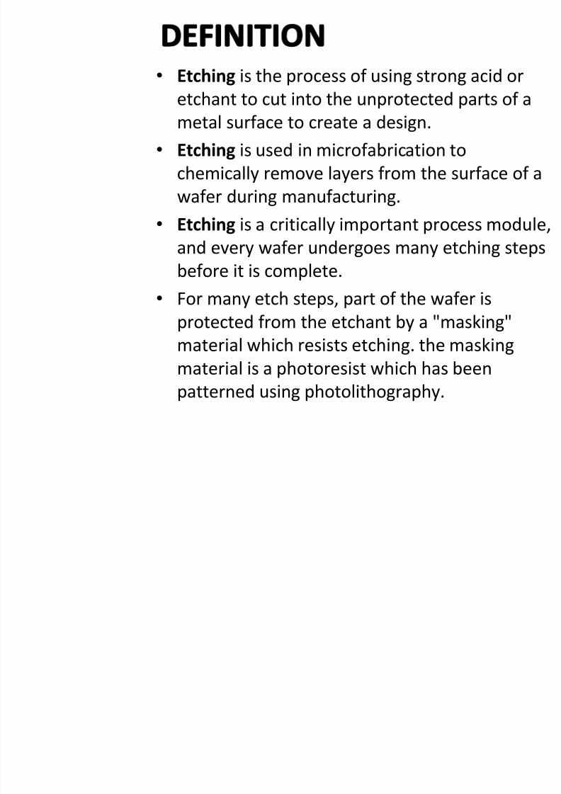
• Etching is the process of using strong acid or
etchant to cut into the unprotected parts of ametal surface to create a design.
• Etching is used in microfabrication to
chemically remove layers from the surface of a
wafer during manufacturing.• Etching is a critically important process module,
and every wafer undergoes many etching steps
before it is complete.
• For many etch steps, part of the wafer isprotected from the etchant by a "masking"
material which resists etching. the masking
material is a photoresist which has been
patterned using photolithography.

7/29/2019 2 5 Integrated Circuit Fabrication Process Etching Student
http://slidepdf.com/reader/full/2-5-integrated-circuit-fabrication-process-etching-student 4/16
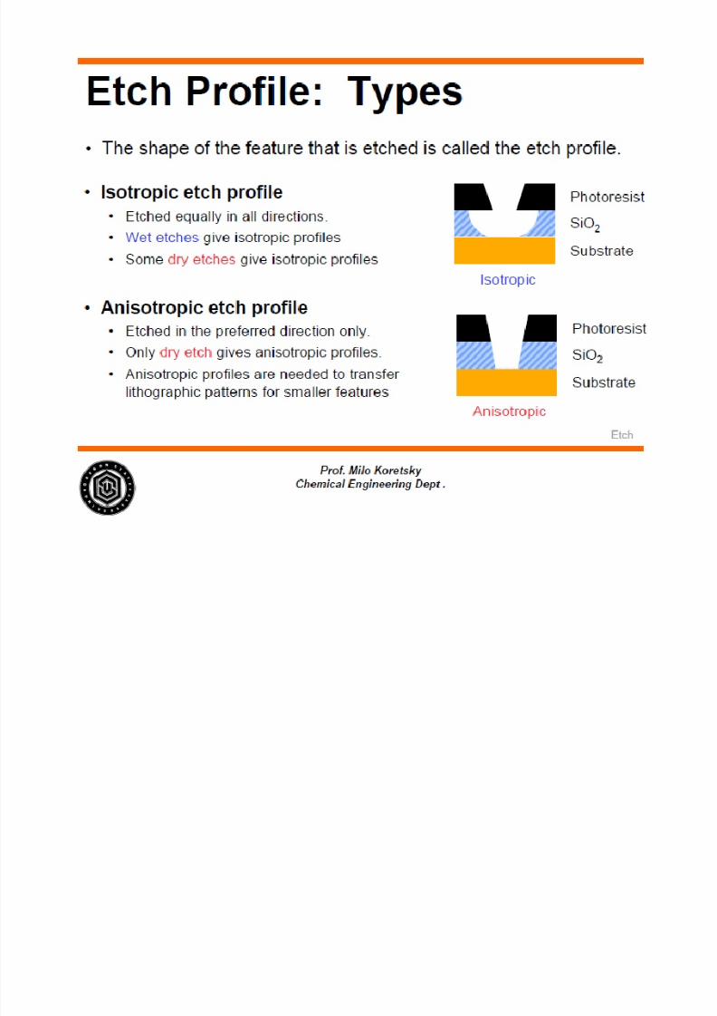
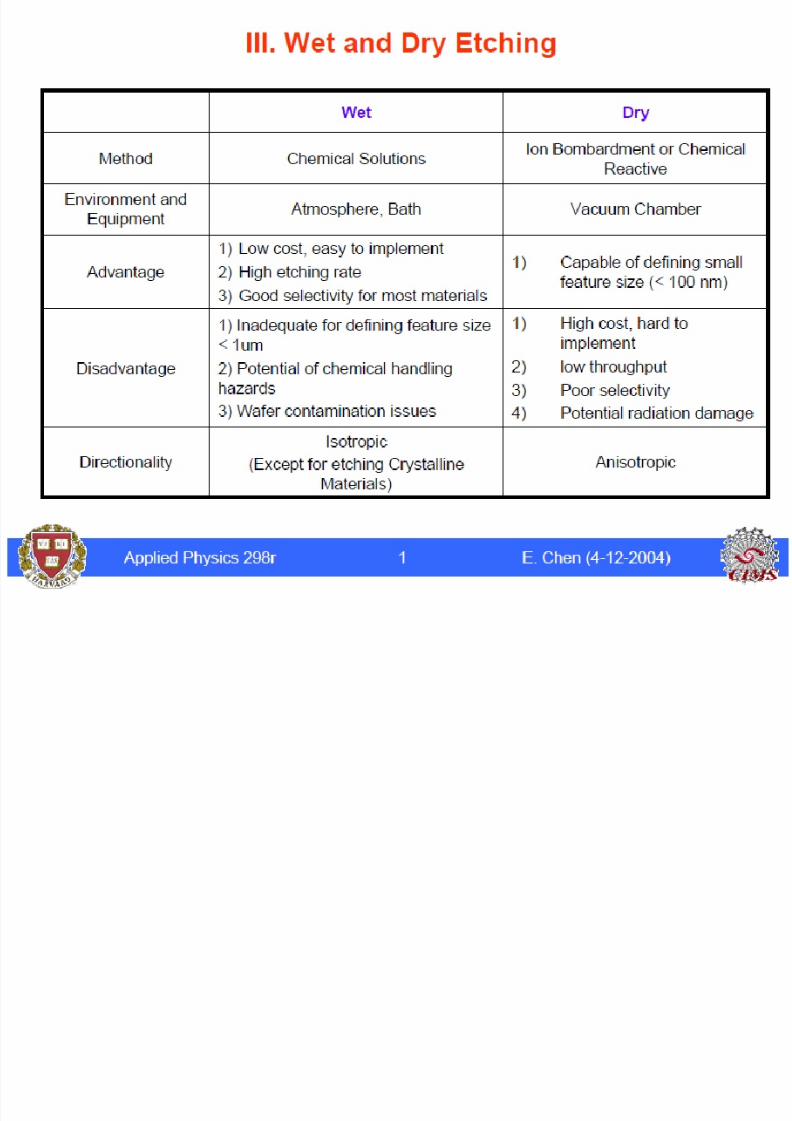
• Two main methods of etching:
• wet etching
• dry etching
7/29/2019 2 5 Integrated Circuit Fabrication Process Etching Student
http://slidepdf.com/reader/full/2-5-integrated-circuit-fabrication-process-etching-student 5/16
1. In wafer formation process, after slicing ingot
to removed any remaining damaged and
contaminated regions.2. In photolithography process to removed
unnecessary photoresist.
3. In metallization process to removedunnecessary metal surface for making
contact between devices.
7/29/2019 2 5 Integrated Circuit Fabrication Process Etching Student
http://slidepdf.com/reader/full/2-5-integrated-circuit-fabrication-process-etching-student 6/16
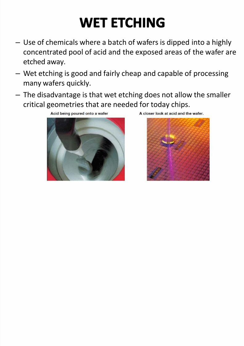
– Use of chemicals where a batch of wafers is dipped into a highlyconcentrated pool of acid and the exposed areas of the wafer are
etched away.
– Wet etching is good and fairly cheap and capable of processing
many wafers quickly. – The disadvantage is that wet etching does not allow the smaller
critical geometries that are needed for today chips.
7/29/2019 2 5 Integrated Circuit Fabrication Process Etching Student
http://slidepdf.com/reader/full/2-5-integrated-circuit-fabrication-process-etching-student 7/16
• Dry etching refers to any of the methods of etching that use gas instead of chemical
etchants.• Dry etching is capable of producing critical
geometries that are very small.
• Ex: Plasma Etching
– Reactive Ion Etching in 80’s
• Ex: Electron Cyclotron Resonance (ECR) andInductively Coupled Plasmas (ICP) in 90’s.

7/29/2019 2 5 Integrated Circuit Fabrication Process Etching Student
http://slidepdf.com/reader/full/2-5-integrated-circuit-fabrication-process-etching-student 8/16
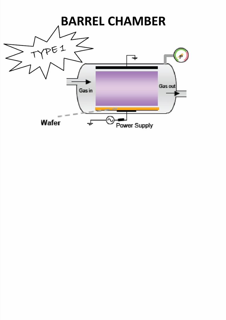
PLASMA ETCHING
• Plasma etching uses a gas that is subjected to anintense electric field to generate the plasma state.
• The electric field is produced with coils that arewrapped around the chamber and exposed to a highlevel RF source.
• There are two different versions of this type of etchingbased on the shape of the chamber used.
1. One consists of a barrel type chamber where the wafersare placed sitting up while the gas is flowed over thewafers and out through an exhaust pipe.
2. The second process uses a parallel plate reactor.
7/29/2019 2 5 Integrated Circuit Fabrication Process Etching Student
http://slidepdf.com/reader/full/2-5-integrated-circuit-fabrication-process-etching-student 9/16
BARREL CHAMBER
7/29/2019 2 5 Integrated Circuit Fabrication Process Etching Student
http://slidepdf.com/reader/full/2-5-integrated-circuit-fabrication-process-etching-student 10/16
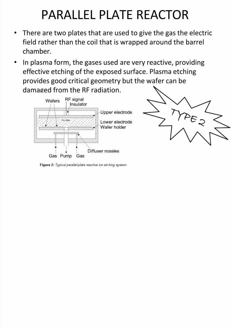
PARALLEL PLATE REACTOR
• There are two plates that are used to give the gas the electric
field rather than the coil that is wrapped around the barrelchamber.
• In plasma form, the gases used are very reactive, providing
effective etching of the exposed surface. Plasma etching
provides good critical geometry but the wafer can bedamaged from the RF radiation.
7/29/2019 2 5 Integrated Circuit Fabrication Process Etching Student
http://slidepdf.com/reader/full/2-5-integrated-circuit-fabrication-process-etching-student 11/16
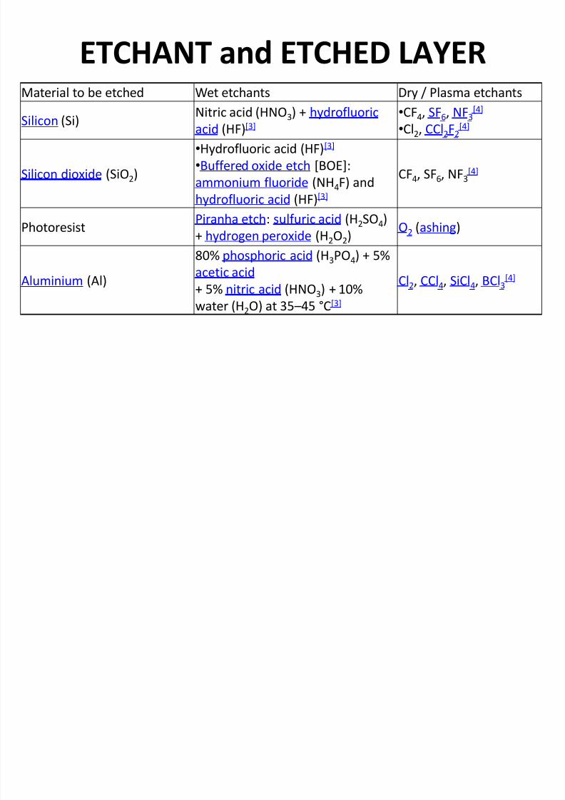
ETCHANT and ETCHED LAYER
Material to be etched Wet etchants Dry / Plasma etchantsSilicon (Si)
Nitric acid (HNO3) + hydrofluoric
acid (HF)[3]
•CF4, SF6, NF3[4]
•Cl2, CCl2F2[4]
Silicon dioxide (SiO2)
•Hydrofluoric acid (HF)[3]
•Buffered oxide etch [BOE]:
ammonium fluoride (NH4F) and
hydrofluoric acid (HF)[3]
CF4, SF6, NF3[4]
PhotoresistPiranha etch: sulfuric acid (H2SO4)
+ hydrogen peroxide (H2O2)O2 (ashing)
Aluminium (Al)
80% phosphoric acid (H3PO4) + 5%
acetic acid
+ 5% nitric acid (HNO3) + 10%
water (H2O) at 35 –45 °C[3]
Cl2, CCl4, SiCl4, BCl3[4]
7/29/2019 2 5 Integrated Circuit Fabrication Process Etching Student
http://slidepdf.com/reader/full/2-5-integrated-circuit-fabrication-process-etching-student 12/16
7/29/2019 2 5 Integrated Circuit Fabrication Process Etching Student
http://slidepdf.com/reader/full/2-5-integrated-circuit-fabrication-process-etching-student 13/16
7/29/2019 2 5 Integrated Circuit Fabrication Process Etching Student
http://slidepdf.com/reader/full/2-5-integrated-circuit-fabrication-process-etching-student 14/16
7/29/2019 2 5 Integrated Circuit Fabrication Process Etching Student
http://slidepdf.com/reader/full/2-5-integrated-circuit-fabrication-process-etching-student 15/16
7/29/2019 2 5 Integrated Circuit Fabrication Process Etching Student
http://slidepdf.com/reader/full/2-5-integrated-circuit-fabrication-process-etching-student 16/16