
1Gb: x4, x8, x16 DDR3 SDRAM - Micron Technology/media/Documents/Products/Data Sheet/DR… · Table...
211
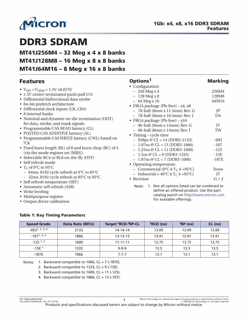
DDR3 SDRAM MT41J256M4 – 32 Meg x 4 x 8 banks MT41J128M8 – 16 Meg x 8 x 8 banks MT41J64M16 – 8 Meg x 16 x 8 banks Features •V DD = V DDQ = 1.5V ±0.075V • 1.5V center-terminated push/pull I/O • Differential bidirectional data strobe •8n-bit prefetch architecture • Differential clock inputs (CK, CK#) • 8 internal banks • Nominal and dynamic on-die termination (ODT) for data, strobe, and mask signals • Programmable CAS READ latency (CL) • POSTED CAS ADDITIVE latency (AL) • Programmable CAS WRITE latency (CWL) based on t CK • Fixed burst length (BL) of 8 and burst chop (BC) of 4 (via the mode register set [MRS]) • Selectable BC4 or BL8 on-the-fly (OTF) • Self refresh mode •T C of 0°C to 95°C – 64ms, 8192 cycle refresh at 0°C to 85°C – 32ms, 8192 cycle refresh at 85°C to 95°C • Self refresh temperature (SRT) • Automatic self refresh (ASR) • Write leveling • Multipurpose register • Output driver calibration Options 1 Marking • Configuration – 256 Meg x 4 256M4 – 128 Meg x 8 128M8 – 64 Meg x 16 64M16 • FBGA package (Pb-free) – x4, x8 – 78-ball (8mm x 11.5mm) Rev. G JP – 78-ball (8mm x 10.5mm) Rev. J DA • FBGA package (Pb-free) – x16 – 96-ball (8mm x 14mm) Rev. G JT – 96-ball (8mm x 14mm) Rev. J TW • Timing – cycle time – 938ps @ CL = 14 (DDR3-2133) -093 – 1.07ns @ CL = 13 (DDR3-1866) -107 – 1.25ns @ CL = 11 (DDR3-1600) -125 – 1.5ns @ CL = 9 (DDR3-1333) -15E – 1.87ns @ CL = 7 (DDR3-1066) -187E • Operating temperature – Commercial (0°C ≤ T C ≤ +95°C) None – Industrial (–40°C ≤ T C ≤ +95°C) IT • Revision :G / :J Note: 1. Not all options listed can be combined to define an offered product. Use the part catalog search on http://www.micron.com for available offerings. Table 1: Key Timing Parameters Speed Grade Data Rate (MT/s) Target t RCD- t RP-CL t RCD (ns) t RP (ns) CL (ns) -093 1, 2, 3, 4 2133 14-14-14 13.09 13.09 13.09 -107 1, 2, 3 1866 13-13-13 13.91 13.91 13.91 -125 1, 2 1600 11-11-11 13.75 13.75 13.75 -15E 1 1333 9-9-9 13.5 13.5 13.5 -187E 1066 7-7-7 13.1 13.1 13.1 Notes: 1. Backward compatible to 1066, CL = 7 (-187E). 2. Backward compatible to 1333, CL = 9 (-15E). 3. Backward compatible to 1600, CL = 11 (-125). 4. Backward compatible to 1866, CL = 13 (-107). 1Gb: x4, x8, x16 DDR3 SDRAM Features PDF: 09005aef826aa906 1Gb_DDR3_SDRAM.pdf - Rev. N 11/14 EN 1 Micron Technology, Inc. reserves the right to change products or specifications without notice. © 2006 Micron Technology, Inc. All rights reserved. Products and specifications discussed herein are subject to change by Micron without notice.
Transcript of 1Gb: x4, x8, x16 DDR3 SDRAM - Micron Technology/media/Documents/Products/Data Sheet/DR… · Table...
DDR3 SDRAMMT41J256M4 – 32 Meg x 4 x 8 banksMT41J128M8 – 16 Meg x 8 x 8 banksMT41J64M16 – 8 Meg x 16 x 8 banks
Features• VDD = VDDQ = 1.5V ±0.075V• 1.5V center-terminated push/pull I/O• Differential bidirectional data strobe• 8n-bit prefetch architecture• Differential clock inputs (CK, CK#)• 8 internal banks• Nominal and dynamic on-die termination (ODT)
for data, strobe, and mask signals• Programmable CAS READ latency (CL)• POSTED CAS ADDITIVE latency (AL)• Programmable CAS WRITE latency (CWL) based on
tCK• Fixed burst length (BL) of 8 and burst chop (BC) of 4
(via the mode register set [MRS])• Selectable BC4 or BL8 on-the-fly (OTF)• Self refresh mode• TC of 0°C to 95°C
– 64ms, 8192 cycle refresh at 0°C to 85°C– 32ms, 8192 cycle refresh at 85°C to 95°C
• Self refresh temperature (SRT)• Automatic self refresh (ASR)• Write leveling• Multipurpose register• Output driver calibration
Options1 Marking• Configuration
– 256 Meg x 4 256M4– 128 Meg x 8 128M8– 64 Meg x 16 64M16
• FBGA package (Pb-free) – x4, x8– 78-ball (8mm x 11.5mm) Rev. G JP– 78-ball (8mm x 10.5mm) Rev. J DA
• FBGA package (Pb-free) – x16– 96-ball (8mm x 14mm) Rev. G JT– 96-ball (8mm x 14mm) Rev. J TW
• Timing – cycle time – 938ps @ CL = 14 (DDR3-2133) -093– 1.07ns @ CL = 13 (DDR3-1866) -107– 1.25ns @ CL = 11 (DDR3-1600) -125– 1.5ns @ CL = 9 (DDR3-1333) -15E– 1.87ns @ CL = 7 (DDR3-1066) -187E
• Operating temperature – Commercial (0°C ≤ TC ≤ +95°C) None– Industrial (–40°C ≤ TC ≤ +95°C) IT
• Revision :G / :J
Note: 1. Not all options listed can be combined todefine an offered product. Use the partcatalog search on http://www.micron.comfor available offerings.
Table 1: Key Timing Parameters
Speed Grade Data Rate (MT/s) Target tRCD-tRP-CL tRCD (ns) tRP (ns) CL (ns)
-0931, 2, 3, 4 2133 14-14-14 13.09 13.09 13.09
-1071, 2, 3 1866 13-13-13 13.91 13.91 13.91
-125 1, 2 1600 11-11-11 13.75 13.75 13.75
-15E 1 1333 9-9-9 13.5 13.5 13.5
-187E 1066 7-7-7 13.1 13.1 13.1
Notes: 1. Backward compatible to 1066, CL = 7 (-187E).2. Backward compatible to 1333, CL = 9 (-15E).3. Backward compatible to 1600, CL = 11 (-125).4. Backward compatible to 1866, CL = 13 (-107).
1Gb: x4, x8, x16 DDR3 SDRAMFeatures
PDF: 09005aef826aa9061Gb_DDR3_SDRAM.pdf - Rev. N 11/14 EN 1 Micron Technology, Inc. reserves the right to change products or specifications without notice.
© 2006 Micron Technology, Inc. All rights reserved.
Products and specifications discussed herein are subject to change by Micron without notice.
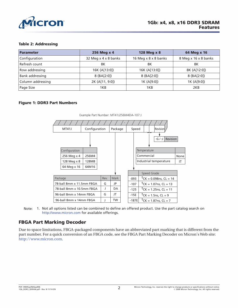
Table 2: Addressing
Parameter 256 Meg x 4 128 Meg x 8 64 Meg x 16
Configuration 32 Meg x 4 x 8 banks 16 Meg x 8 x 8 banks 8 Meg x 16 x 8 banks
Refresh count 8K 8K 8K
Row addressing 16K (A[13:0]) 16K (A[13:0]) 8K (A[12:0])
Bank addressing 8 (BA[2:0]) 8 (BA[2:0]) 8 (BA[2:0])
Column addressing 2K (A[11, 9:0]) 1K (A[9:0]) 1K (A[9:0])
Page Size 1KB 1KB 2KB
Figure 1: DDR3 Part Numbers
Package
78-ball 8mm x 11.5mm FBGA
96-ball 8mm x 14mm FBGA
Mark
JP
JT
Rev.
G
G
Example Part Number: MT41J256M4DA-107:J
Configuration
256 Meg x 4
128 Meg x 8
64 Meg x 16
256M4
128M8
64M16
Speed GradetCK = 0.098ns, CL = 14tCK = 1.07ns, CL = 13tCK = 1.25ns, CL = 11
-093
-107
-125
-
ConfigurationMT41J Package Speed Revision
Revision:G / :J
:
Temperature
Commercial
Industrial temperature
{None
IT
96-ball 8mm x 14mm FBGA J
78-ball 8mm x 10.5mm FBGA J DA
TW
-15E tCK = 1.5ns, CL = 9
-187E tCK = 1.87ns, CL = 7
Note: 1. Not all options listed can be combined to define an offered product. Use the part catalog search onhttp://www.micron.com for available offerings.
FBGA Part Marking Decoder
Due to space limitations, FBGA-packaged components have an abbreviated part marking that is different from thepart number. For a quick conversion of an FBGA code, see the FBGA Part Marking Decoder on Micron’s Web site:http://www.micron.com.
1Gb: x4, x8, x16 DDR3 SDRAMFeatures
PDF: 09005aef826aa9061Gb_DDR3_SDRAM.pdf - Rev. N 11/14 EN 2 Micron Technology, Inc. reserves the right to change products or specifications without notice.
© 2006 Micron Technology, Inc. All rights reserved.
ContentsState Diagram ................................................................................................................................................ 11Functional Description ................................................................................................................................... 12
Industrial Temperature ............................................................................................................................... 12General Notes ............................................................................................................................................ 12
Functional Block Diagrams ............................................................................................................................. 14Ball Assignments and Descriptions ................................................................................................................. 16Package Dimensions ....................................................................................................................................... 22Electrical Specifications .................................................................................................................................. 26
Absolute Ratings ......................................................................................................................................... 26Input/Output Capacitance .......................................................................................................................... 27
Thermal Characteristics .................................................................................................................................. 28Electrical Specifications – I DD Specifications and Conditions ........................................................................... 30Electrical Characteristics – IDD Specifications .................................................................................................. 41Electrical Specifications – DC and AC .............................................................................................................. 44
DC Operating Conditions ........................................................................................................................... 44Input Operating Conditions ........................................................................................................................ 44AC Overshoot/Undershoot Specification ..................................................................................................... 48Slew Rate Definitions for Single-Ended Input Signals ................................................................................... 51Slew Rate Definitions for Differential Input Signals ...................................................................................... 53
ODT Characteristics ....................................................................................................................................... 54ODT Resistors ............................................................................................................................................ 55ODT Sensitivity .......................................................................................................................................... 56ODT Timing Definitions ............................................................................................................................. 56
Output Driver Impedance ............................................................................................................................... 6034 Ohm Output Driver Impedance .............................................................................................................. 6134 Ohm Driver ............................................................................................................................................ 6234 Ohm Output Driver Sensitivity ................................................................................................................ 63Alternative 40 Ohm Driver .......................................................................................................................... 6440 Ohm Output Driver Sensitivity ................................................................................................................ 64
Output Characteristics and Operating Conditions ............................................................................................ 66Reference Output Load ............................................................................................................................... 68Slew Rate Definitions for Single-Ended Output Signals ................................................................................. 69Slew Rate Definitions for Differential Output Signals .................................................................................... 70
Speed Bin Tables ............................................................................................................................................ 71Electrical Characteristics and AC Operating Conditions ................................................................................... 76Command and Address Setup, Hold, and Derating ........................................................................................... 96Data Setup, Hold, and Derating ...................................................................................................................... 104Commands – Truth Tables ............................................................................................................................. 113Commands ................................................................................................................................................... 116
DESELECT ................................................................................................................................................ 116NO OPERATION ........................................................................................................................................ 116ZQ CALIBRATION LONG ........................................................................................................................... 116ZQ CALIBRATION SHORT .......................................................................................................................... 116ACTIVATE ................................................................................................................................................. 116READ ........................................................................................................................................................ 116WRITE ...................................................................................................................................................... 117PRECHARGE ............................................................................................................................................. 118REFRESH .................................................................................................................................................. 118SELF REFRESH .......................................................................................................................................... 119DLL Disable Mode ..................................................................................................................................... 120
1Gb: x4, x8, x16 DDR3 SDRAMFeatures
PDF: 09005aef826aa9061Gb_DDR3_SDRAM.pdf - Rev. N 11/14 EN 3 Micron Technology, Inc. reserves the right to change products or specifications without notice.
© 2006 Micron Technology, Inc. All rights reserved.
Input Clock Frequency Change ...................................................................................................................... 124Write Leveling ............................................................................................................................................... 126
Write Leveling Procedure ........................................................................................................................... 128Write Leveling Mode Exit Procedure ........................................................................................................... 130
Initialization ................................................................................................................................................. 131Mode Registers .............................................................................................................................................. 133Mode Register 0 (MR0) ................................................................................................................................... 134
Burst Length ............................................................................................................................................. 134Burst Type ................................................................................................................................................. 135DLL RESET ................................................................................................................................................ 136Write Recovery .......................................................................................................................................... 136Precharge Power-Down (Precharge PD) ...................................................................................................... 137CAS Latency (CL) ....................................................................................................................................... 137
Mode Register 1 (MR1) ................................................................................................................................... 138DLL Enable/DLL Disable ........................................................................................................................... 138Output Drive Strength ............................................................................................................................... 139OUTPUT ENABLE/DISABLE ...................................................................................................................... 139TDQS Enable ............................................................................................................................................. 139On-Die Termination .................................................................................................................................. 140WRITE LEVELING ..................................................................................................................................... 140POSTED CAS ADDITIVE Latency ................................................................................................................ 140
Mode Register 2 (MR2) ................................................................................................................................... 141CAS Write Latency (CWL) ........................................................................................................................... 142AUTO SELF REFRESH (ASR) ....................................................................................................................... 142SELF REFRESH TEMPERATURE (SRT) ........................................................................................................ 143SRT vs. ASR ............................................................................................................................................... 143DYNAMIC ODT ......................................................................................................................................... 143
Mode Register 3 (MR3) ................................................................................................................................... 144MULTIPURPOSE REGISTER (MPR) ............................................................................................................ 144MPR Functional Description ...................................................................................................................... 145MPR Register Address Definitions and Bursting Order ................................................................................. 146MPR Read Predefined Pattern .................................................................................................................... 152
MODE REGISTER SET (MRS) Command ........................................................................................................ 152ZQ CALIBRATION Operation ......................................................................................................................... 153ACTIVATE Operation ..................................................................................................................................... 154READ Operation ............................................................................................................................................ 156WRITE Operation .......................................................................................................................................... 167
DQ Input Timing ....................................................................................................................................... 175PRECHARGE Operation ................................................................................................................................. 177SELF REFRESH Operation .............................................................................................................................. 177Extended Temperature Usage ........................................................................................................................ 179Power-Down Mode ........................................................................................................................................ 180RESET Operation ........................................................................................................................................... 188On-Die Termination (ODT) ............................................................................................................................ 190
Functional Representation of ODT ............................................................................................................. 190Nominal ODT ............................................................................................................................................ 190
Dynamic ODT ............................................................................................................................................... 192Dynamic ODT Special Use Case ................................................................................................................. 192Functional Description .............................................................................................................................. 192
Synchronous ODT Mode ................................................................................................................................ 198ODT Latency and Posted ODT .................................................................................................................... 198Timing Parameters .................................................................................................................................... 198
1Gb: x4, x8, x16 DDR3 SDRAMFeatures
PDF: 09005aef826aa9061Gb_DDR3_SDRAM.pdf - Rev. N 11/14 EN 4 Micron Technology, Inc. reserves the right to change products or specifications without notice.
© 2006 Micron Technology, Inc. All rights reserved.
ODT Off During READs .............................................................................................................................. 201Asynchronous ODT Mode .............................................................................................................................. 203
Synchronous to Asynchronous ODT Mode Transition (Power-Down Entry) .................................................. 205Asynchronous to Synchronous ODT Mode Transition (Power-Down Exit) ........................................................ 207
Asynchronous to Synchronous ODT Mode Transition (Short CKE Pulse) ...................................................... 209
1Gb: x4, x8, x16 DDR3 SDRAMFeatures
PDF: 09005aef826aa9061Gb_DDR3_SDRAM.pdf - Rev. N 11/14 EN 5 Micron Technology, Inc. reserves the right to change products or specifications without notice.
© 2006 Micron Technology, Inc. All rights reserved.
List of TablesTable 1: Key Timing Parameters ....................................................................................................................... 1Table 2: Addressing ......................................................................................................................................... 2Table 3: 78-Ball FBGA – x4, x8 Ball Descriptions .............................................................................................. 18Table 4: 96-Ball FBGA – x16 Ball Descriptions ................................................................................................. 20Table 5: Absolute Maximum Ratings .............................................................................................................. 26Table 6: DDR3 Input/Output Capacitance ...................................................................................................... 27Table 7: Thermal Characteristics .................................................................................................................... 28Table 8: Timing Parameters Used for IDD Measurements – Clock Units ............................................................ 30Table 9: IDD0 Measurement Loop ................................................................................................................... 31Table 10: IDD1 Measurement Loop .................................................................................................................. 32Table 11: IDD Measurement Conditions for Power-Down Currents ................................................................... 33Table 12: IDD2N and IDD3N Measurement Loop ................................................................................................ 34Table 13: IDD2NT Measurement Loop .............................................................................................................. 34Table 14: IDD4R Measurement Loop ................................................................................................................ 35Table 15: IDD4W Measurement Loop ............................................................................................................... 36Table 16: IDD5B Measurement Loop ................................................................................................................ 37Table 17: IDD Measurement Conditions for IDD6, IDD6ET, and IDD8 .................................................................... 38Table 18: IDD7 Measurement Loop .................................................................................................................. 39Table 19: IDD Maximum Limits – Rev. G .......................................................................................................... 41Table 20: IDD Maximum Limits – Rev. J ........................................................................................................... 42Table 21: DC Electrical Characteristics and Operating Conditions ................................................................... 44Table 22: DC Electrical Characteristics and Input Conditions .......................................................................... 44Table 23: Input Switching Conditions ............................................................................................................. 45Table 24: Differential Input Operating Conditions (CK, CK# and DQS, DQS#) .................................................. 46Table 25: Control and Address Pins ................................................................................................................ 48Table 26: Clock, Data, Strobe, and Mask Pins .................................................................................................. 48Table 27: Allowed Time Before Ringback (tDVAC) for CK - CK# and DQS - DQS# ............................................... 50Table 28: Single-Ended Input Slew Rate Definition .......................................................................................... 51Table 29: Differential Input Slew Rate Definition ............................................................................................. 53Table 30: On-Die Termination DC Electrical Characteristics ............................................................................ 54Table 31: RTT Effective Impedances ................................................................................................................ 55Table 32: ODT Sensitivity Definition .............................................................................................................. 56Table 33: ODT Temperature and Voltage Sensitivity ........................................................................................ 56Table 34: ODT Timing Definitions .................................................................................................................. 57Table 35: Reference Settings for ODT Timing Measurements ........................................................................... 57Table 36: 34 Ohm Driver Impedance Characteristics ....................................................................................... 61Table 37: 34 Ohm Driver Pull-Up and Pull-Down Impedance Calculations ....................................................... 62Table 38: 34 Ohm Driver IOH/IOL Characteristics: VDD = VDDQ = 1.5V ................................................................ 62Table 39: 34 Ohm Driver IOH/IOL Characteristics: VDD = VDDQ = 1.575V ............................................................. 62Table 40: 34 Ohm Driver IOH/IOL Characteristics: VDD = VDDQ = 1.425V ............................................................. 63Table 41: 34 Ohm Output Driver Sensitivity Definition .................................................................................... 63Table 42: 34 Ohm Output Driver Voltage and Temperature Sensitivity .............................................................. 63Table 43: 40 Ohm Driver Impedance Characteristics ....................................................................................... 64Table 44: 40 Ohm Output Driver Sensitivity Definition .................................................................................... 64Table 45: 40 Ohm Output Driver Voltage and Temperature Sensitivity .............................................................. 65Table 46: Single-Ended Output Driver Characteristics ..................................................................................... 66Table 47: Differential Output Driver Characteristics ........................................................................................ 67Table 48: Single-Ended Output Slew Rate Definition ....................................................................................... 69Table 49: Differential Output Slew Rate Definition .......................................................................................... 70Table 50: DDR3-1066 Speed Bins ................................................................................................................... 71
1Gb: x4, x8, x16 DDR3 SDRAMFeatures
PDF: 09005aef826aa9061Gb_DDR3_SDRAM.pdf - Rev. N 11/14 EN 6 Micron Technology, Inc. reserves the right to change products or specifications without notice.
© 2006 Micron Technology, Inc. All rights reserved.
Table 51: DDR3-1333 Speed Bins ................................................................................................................... 72Table 52: DDR3-1600 Speed Bins ................................................................................................................... 73Table 53: DDR3-1866 Speed Bins ................................................................................................................... 74Table 54: DDR3-2133 Speed Bins ................................................................................................................... 75Table 55: Electrical Characteristics and AC Operating Conditions .................................................................... 76Table 56: Electrical Characteristics and AC Operating Conditions for Speed Extensions .................................... 86Table 57: Command and Address Setup and Hold Values Referenced – AC/DC-Based ...................................... 96Table 58: Derating Values for tIS/tIH – AC175/DC100-Based ............................................................................ 97Table 59: Derating Values for tIS/tIH – AC150/DC100-Based ............................................................................ 97Table 60: Derating Values for tIS/tIH – AC135/DC100-Based ............................................................................ 98Table 61: Derating Values for tIS/tIH – AC125/DC100-Based ............................................................................ 98Table 62: Minimum Required Time tVAC Above VIH(AC) or Below VIL(AC)for Valid Transition ............................... 99Table 63: DDR3 Data Setup and Hold Values at 1 V/ns (DQS, DQS# at 2 V/ns) – AC/DC-Based ......................... 104Table 64: Derating Values for tDS/tDH – AC175/DC100-Based ........................................................................ 105Table 65: Derating Values for tDS/tDH – AC150/DC100-Based ........................................................................ 105Table 66: Derating Values for tDS/tDH – AC135/DC100-Based at 1V/ns ........................................................... 106Table 67: Derating Values for tDS/tDH – AC135/DC100-Based at 2V/ns ........................................................... 107Table 68: Required Minimum Time tVAC Above VIH(AC) (Below VIL(AC)) for Valid DQ Transition ......................... 108Table 69: Truth Table – Command ................................................................................................................. 113Table 70: Truth Table – CKE .......................................................................................................................... 115Table 71: READ Command Summary ............................................................................................................ 117Table 72: WRITE Command Summary .......................................................................................................... 117Table 73: READ Electrical Characteristics, DLL Disable Mode ......................................................................... 123Table 74: Write Leveling Matrix ..................................................................................................................... 127Table 75: Burst Order .................................................................................................................................... 136Table 76: MPR Functional Description of MR3 Bits ........................................................................................ 145Table 77: MPR Readouts and Burst Order Bit Mapping ................................................................................... 146Table 78: Self Refresh Temperature and Auto Self Refresh Description ............................................................ 179Table 79: Self Refresh Mode Summary ........................................................................................................... 179Table 80: Command to Power-Down Entry Parameters .................................................................................. 180Table 81: Power-Down Modes ....................................................................................................................... 181Table 82: Truth Table – ODT (Nominal) ......................................................................................................... 191Table 83: ODT Parameters ............................................................................................................................ 191Table 84: Write Leveling with Dynamic ODT Special Case .............................................................................. 192Table 85: Dynamic ODT Specific Parameters ................................................................................................. 193Table 86: Mode Registers for RTT,nom ............................................................................................................. 193Table 87: Mode Registers for RTT(WR) ............................................................................................................. 194Table 88: Timing Diagrams for Dynamic ODT ................................................................................................ 194Table 89: Synchronous ODT Parameters ........................................................................................................ 199Table 90: Asynchronous ODT Timing Parameters for All Speed Bins ............................................................... 204Table 91: ODT Parameters for Power-Down (DLL Off) Entry and Exit Transition Period ................................... 206
1Gb: x4, x8, x16 DDR3 SDRAMFeatures
PDF: 09005aef826aa9061Gb_DDR3_SDRAM.pdf - Rev. N 11/14 EN 7 Micron Technology, Inc. reserves the right to change products or specifications without notice.
© 2006 Micron Technology, Inc. All rights reserved.
List of FiguresFigure 1: DDR3 Part Numbers .......................................................................................................................... 2Figure 2: Simplified State Diagram ................................................................................................................. 11Figure 3: 256 Meg x 4 Functional Block Diagram ............................................................................................. 14Figure 4: 128 Meg x 8 Functional Block Diagram ............................................................................................. 15Figure 5: 64 Meg x 16 Functional Block Diagram ............................................................................................. 15Figure 6: 78-Ball FBGA – x4, x8 (Top View) ...................................................................................................... 16Figure 7: 96-Ball FBGA – x16 (Top View) ......................................................................................................... 17Figure 8: 78-Ball FBGA – x4, x8 (JP) ................................................................................................................ 22Figure 9: 78-Ball FBGA – x4, x8 (DA) ............................................................................................................... 23Figure 10: 96-Ball FBGA – x16 (JT) .................................................................................................................. 24Figure 11: 96-Ball FBGA – x16 (TW) ................................................................................................................ 25Figure 12: Thermal Measurement Point ......................................................................................................... 29Figure 13: Input Signal .................................................................................................................................. 47Figure 14: Overshoot ..................................................................................................................................... 48Figure 15: Undershoot ................................................................................................................................... 48Figure 16: VIX for Differential Signals .............................................................................................................. 49Figure 17: Single-Ended Requirements for Differential Signals ........................................................................ 49Figure 18: Definition of Differential AC-Swing and tDVAC ............................................................................... 50Figure 19: Nominal Slew Rate Definition for Single-Ended Input Signals .......................................................... 52Figure 20: Nominal Differential Input Slew Rate Definition for DQS, DQS# and CK, CK# .................................. 53Figure 21: ODT Levels and I-V Characteristics ................................................................................................ 54Figure 22: ODT Timing Reference Load .......................................................................................................... 57Figure 23: tAON and tAOF Definitions ............................................................................................................ 58Figure 24: tAONPD and tAOFPD Definitions ................................................................................................... 58Figure 25: tADC Definition ............................................................................................................................. 59Figure 26: Output Driver ................................................................................................................................ 60Figure 27: DQ Output Signal .......................................................................................................................... 67Figure 28: Differential Output Signal .............................................................................................................. 68Figure 29: Reference Output Load for AC Timing and Output Slew Rate ........................................................... 68Figure 30: Nominal Slew Rate Definition for Single-Ended Output Signals ....................................................... 69Figure 31: Nominal Differential Output Slew Rate Definition for DQS, DQS# .................................................... 70Figure 32: Nominal Slew Rate and tVAC for tIS (Command and Address – Clock) ............................................. 100Figure 33: Nominal Slew Rate for tIH (Command and Address – Clock) ........................................................... 101Figure 34: Tangent Line for tIS (Command and Address – Clock) .................................................................... 102Figure 35: Tangent Line for tIH (Command and Address – Clock) .................................................................... 103Figure 36: Nominal Slew Rate and tVAC for tDS (DQ – Strobe) ......................................................................... 109Figure 37: Nominal Slew Rate for tDH (DQ – Strobe) ...................................................................................... 110Figure 38: Tangent Line for tDS (DQ – Strobe) ................................................................................................ 111Figure 39: Tangent Line for tDH (DQ – Strobe) ............................................................................................... 112Figure 40: Refresh Mode ............................................................................................................................... 119Figure 41: DLL Enable Mode to DLL Disable Mode ........................................................................................ 121Figure 42: DLL Disable Mode to DLL Enable Mode ........................................................................................ 122Figure 43: DLL Disable tDQSCK .................................................................................................................... 123Figure 44: Change Frequency During Precharge Power-Down ........................................................................ 125Figure 45: Write Leveling Concept ................................................................................................................. 126Figure 46: Write Leveling Sequence ............................................................................................................... 129Figure 47: Write Leveling Exit Procedure ....................................................................................................... 130Figure 48: Initialization Sequence ................................................................................................................. 132Figure 49: MRS to MRS Command Timing (tMRD) ......................................................................................... 133Figure 50: MRS to nonMRS Command Timing (tMOD) .................................................................................. 134
1Gb: x4, x8, x16 DDR3 SDRAMFeatures
PDF: 09005aef826aa9061Gb_DDR3_SDRAM.pdf - Rev. N 11/14 EN 8 Micron Technology, Inc. reserves the right to change products or specifications without notice.
© 2006 Micron Technology, Inc. All rights reserved.
Figure 51: Mode Register 0 (MR0) Definitions ................................................................................................ 135Figure 52: READ Latency .............................................................................................................................. 137Figure 53: Mode Register 1 (MR1) Definition ................................................................................................. 138Figure 54: READ Latency (AL = 5, CL = 6) ....................................................................................................... 141Figure 55: Mode Register 2 (MR2) Definition ................................................................................................. 142Figure 56: CAS Write Latency ........................................................................................................................ 142Figure 57: Mode Register 3 (MR3) Definition ................................................................................................. 144Figure 58: Multipurpose Register (MPR) Block Diagram ................................................................................. 145Figure 59: MPR System Read Calibration with BL8: Fixed Burst Order Single Readout ..................................... 148Figure 60: MPR System Read Calibration with BL8: Fixed Burst Order, Back-to-Back Readout .......................... 149Figure 61: MPR System Read Calibration with BC4: Lower Nibble, Then Upper Nibble .................................... 150Figure 62: MPR System Read Calibration with BC4: Upper Nibble, Then Lower Nibble .................................... 151Figure 63: ZQ CALIBRATION Timing (ZQCL and ZQCS) ................................................................................. 153Figure 64: Example: Meeting tRRD (MIN) and tRCD (MIN) ............................................................................. 154Figure 65: Example: tFAW ............................................................................................................................. 155Figure 66: READ Latency .............................................................................................................................. 156Figure 67: Consecutive READ Bursts (BL8) .................................................................................................... 158Figure 68: Consecutive READ Bursts (BC4) .................................................................................................... 158Figure 69: Nonconsecutive READ Bursts ....................................................................................................... 159Figure 70: READ (BL8) to WRITE (BL8) .......................................................................................................... 159Figure 71: READ (BC4) to WRITE (BC4) OTF .................................................................................................. 160Figure 72: READ to PRECHARGE (BL8) .......................................................................................................... 160Figure 73: READ to PRECHARGE (BC4) ......................................................................................................... 161Figure 74: READ to PRECHARGE (AL = 5, CL = 6) ........................................................................................... 161Figure 75: READ with Auto Precharge (AL = 4, CL = 6) ..................................................................................... 161Figure 76: Data Output Timing – tDQSQ and Data Valid Window .................................................................... 163Figure 77: Data Strobe Timing – READs ......................................................................................................... 164Figure 78: Method for Calculating tLZ and tHZ ............................................................................................... 165Figure 79: tRPRE Timing ............................................................................................................................... 165Figure 80: tRPST Timing ............................................................................................................................... 166Figure 81: tWPRE Timing .............................................................................................................................. 168Figure 82: tWPST Timing .............................................................................................................................. 168Figure 83: WRITE Burst ................................................................................................................................ 169Figure 84: Consecutive WRITE (BL8) to WRITE (BL8) ..................................................................................... 170Figure 85: Consecutive WRITE (BC4) to WRITE (BC4) via OTF ........................................................................ 170Figure 86: Nonconsecutive WRITE to WRITE ................................................................................................. 171Figure 87: WRITE (BL8) to READ (BL8) .......................................................................................................... 171Figure 88: WRITE to READ (BC4 Mode Register Setting) ................................................................................. 172Figure 89: WRITE (BC4 OTF) to READ (BC4 OTF) ........................................................................................... 173Figure 90: WRITE (BL8) to PRECHARGE ........................................................................................................ 174Figure 91: WRITE (BC4 Mode Register Setting) to PRECHARGE ...................................................................... 174Figure 92: WRITE (BC4 OTF) to PRECHARGE ................................................................................................ 175Figure 93: Data Input Timing ........................................................................................................................ 176Figure 94: Self Refresh Entry/Exit Timing ...................................................................................................... 178Figure 95: Active Power-Down Entry and Exit ................................................................................................ 182Figure 96: Precharge Power-Down (Fast-Exit Mode) Entry and Exit ................................................................. 182Figure 97: Precharge Power-Down (Slow-Exit Mode) Entry and Exit ................................................................ 183Figure 98: Power-Down Entry After READ or READ with Auto Precharge (RDAP) ............................................. 183Figure 99: Power-Down Entry After WRITE .................................................................................................... 184Figure 100: Power-Down Entry After WRITE with Auto Precharge (WRAP) ...................................................... 184Figure 101: REFRESH to Power-Down Entry .................................................................................................. 185Figure 102: ACTIVATE to Power-Down Entry ................................................................................................. 185
1Gb: x4, x8, x16 DDR3 SDRAMFeatures
PDF: 09005aef826aa9061Gb_DDR3_SDRAM.pdf - Rev. N 11/14 EN 9 Micron Technology, Inc. reserves the right to change products or specifications without notice.
© 2006 Micron Technology, Inc. All rights reserved.
Figure 103: PRECHARGE to Power-Down Entry ............................................................................................. 186Figure 104: MRS Command to Power-Down Entry ......................................................................................... 186Figure 105: Power-Down Exit to Refresh to Power-Down Entry ....................................................................... 187Figure 106: RESET Sequence ......................................................................................................................... 189Figure 107: On-Die Termination ................................................................................................................... 190Figure 108: Dynamic ODT: ODT Asserted Before and After the WRITE, BC4 .................................................... 195Figure 109: Dynamic ODT: Without WRITE Command .................................................................................. 195Figure 110: Dynamic ODT: ODT Pin Asserted Together with WRITE Command for 6 Clock Cycles, BL8 ............ 196Figure 111: Dynamic ODT: ODT Pin Asserted with WRITE Command for 6 Clock Cycles, BC4 .......................... 197Figure 112: Dynamic ODT: ODT Pin Asserted with WRITE Command for 4 Clock Cycles, BC4 .......................... 197Figure 113: Synchronous ODT ...................................................................................................................... 199Figure 114: Synchronous ODT (BC4) ............................................................................................................. 200Figure 115: ODT During READs .................................................................................................................... 202Figure 116: Asynchronous ODT Timing with Fast ODT Transition .................................................................. 204Figure 117: Synchronous to Asynchronous Transition During Precharge Power-Down (DLL Off) Entry ............ 206Figure 118: Asynchronous to Synchronous Transition During Precharge Power-Down (DLL Off) Exit ............... 208Figure 119: Transition Period for Short CKE LOW Cycles with Entry and Exit Period Overlapping ..................... 210Figure 120: Transition Period for Short CKE HIGH Cycles with Entry and Exit Period Overlapping ................... 210
1Gb: x4, x8, x16 DDR3 SDRAMFeatures
PDF: 09005aef826aa9061Gb_DDR3_SDRAM.pdf - Rev. N 11/14 EN 10 Micron Technology, Inc. reserves the right to change products or specifications without notice.
© 2006 Micron Technology, Inc. All rights reserved.
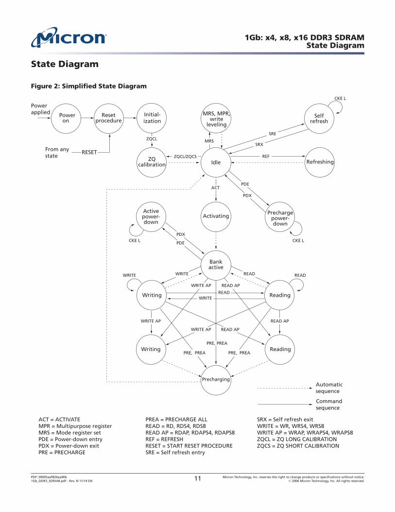
State Diagram
Figure 2: Simplified State Diagram
SRX = Self refresh exitWRITE = WR, WRS4, WRS8WRITE AP = WRAP, WRAPS4, WRAPS8ZQCL = ZQ LONG CALIBRATIONZQCS = ZQ SHORT CALIBRATION
Bankactive
ReadingWriting
Activating
Refreshing
Selfrefresh
Idle
Active power-down
ZQcalibration
From anystate
Powerapplied Reset
procedure Power
onInitial-ization
MRS, MPR, write
leveling
Prechargepower-down
Writing Reading
Automaticsequence
Commandsequence
Precharging
READ
READ READ
READ AP
READ AP
READ AP
PRE, PREA
PRE, PREA PRE, PREA
WRITE
WRITE
CKE L CKE L
CKE L
WRITE
WRITE AP
WRITE AP
WRITE AP
PDE
PDE
PDX
PDX
SRX
SRE
REF
MRS
ACT
RESET
ZQCL
ZQCL/ZQCS
ACT = ACTIVATEMPR = Multipurpose registerMRS = Mode register setPDE = Power-down entryPDX = Power-down exitPRE = PRECHARGE
PREA = PRECHARGE ALLREAD = RD, RDS4, RDS8 READ AP = RDAP, RDAPS4, RDAPS8REF = REFRESHRESET = START RESET PROCEDURESRE = Self refresh entry
1Gb: x4, x8, x16 DDR3 SDRAMState Diagram
PDF: 09005aef826aa9061Gb_DDR3_SDRAM.pdf - Rev. N 11/14 EN 11 Micron Technology, Inc. reserves the right to change products or specifications without notice.
© 2006 Micron Technology, Inc. All rights reserved.
Functional DescriptionDDR3 SDRAM uses a double data rate architecture to achieve high-speed operation.The double data rate architecture is an 8n-prefetch architecture with an interface de-signed to transfer two data words per clock cycle at the I/O pins. A single read or writeoperation for the DDR3 SDRAM effectively consists of a single 8n-bit-wide, four-clock-cycle data transfer at the internal DRAM core and eight corresponding n-bit-wide, one-half-clock-cycle data transfers at the I/O pins.
The differential data strobe (DQS, DQS#) is transmitted externally, along with data, foruse in data capture at the DDR3 SDRAM input receiver. DQS is center-aligned with datafor WRITEs. The read data is transmitted by the DDR3 SDRAM and edge-aligned to thedata strobes.
The DDR3 SDRAM operates from a differential clock (CK and CK#). The crossing of CKgoing HIGH and CK# going LOW is referred to as the positive edge of CK. Control, com-mand, and address signals are registered at every positive edge of CK. Input data is reg-istered on the first rising edge of DQS after the WRITE preamble, and output data is ref-erenced on the first rising edge of DQS after the READ preamble.
Read and write accesses to the DDR3 SDRAM are burst-oriented. Accesses start at a se-lected location and continue for a programmed number of locations in a programmedsequence. Accesses begin with the registration of an ACTIVATE command, which is thenfollowed by a READ or WRITE command. The address bits registered coincident withthe ACTIVATE command are used to select the bank and row to be accessed. The ad-dress bits registered coincident with the READ or WRITE commands are used to selectthe bank and the starting column location for the burst access.
The device uses a READ and WRITE BL8 and BC4. An auto precharge function may beenabled to provide a self-timed row precharge that is initiated at the end of the burstaccess.
As with standard DDR SDRAM, the pipelined, multibank architecture of DDR3 SDRAMallows for concurrent operation, thereby providing high bandwidth by hiding row pre-charge and activation time.
A self refresh mode is provided, along with a power-saving, power-down mode.
Industrial Temperature
The industrial temperature (IT) device requires that the case temperature not exceed–40°C or 95°C. JEDEC specifications require the refresh rate to double when TC exceeds85°C; this also requires use of the high-temperature self refresh option. Additionally,ODT resistance and the input/output impedance must be derated when TC is < 0°C or>95°C.
General Notes
• The functionality and the timing specifications discussed in this data sheet are for theDLL enable mode of operation (normal operation).
• Throughout this data sheet, various figures and text refer to DQs as “DQ.” DQ is to beinterpreted as any and all DQ collectively, unless specifically stated otherwise.
• The terms “DQS” and “CK” found throughout this data sheet are to be interpreted asDQS, DQS# and CK, CK# respectively, unless specifically stated otherwise.
1Gb: x4, x8, x16 DDR3 SDRAMFunctional Description
PDF: 09005aef826aa9061Gb_DDR3_SDRAM.pdf - Rev. N 11/14 EN 12 Micron Technology, Inc. reserves the right to change products or specifications without notice.
© 2006 Micron Technology, Inc. All rights reserved.
• Complete functionality may be described throughout the document; any page or dia-gram may have been simplified to convey a topic and may not be inclusive of all re-quirements.
• Any specific requirement takes precedence over a general statement.• Any functionality not specifically stated is considered undefined, illegal, and not sup-
ported, and can result in unknown operation.• Row addressing is denoted as A[n:0]. For example, 1Gb: n = 12 (x16); 1Gb: n = 13 (x4,
x8); 2Gb: n = 13 (x16) and 2Gb: n = 14 (x4, x8); 4Gb: n = 14 (x16); and 4Gb: n = 15 (x4,x8).
• Dynamic ODT has a special use case: when DDR3 devices are architected for use in asingle rank memory array, the ODT ball can be wired HIGH rather than routed. Referto the Dynamic ODT Special Use Case section.
• A x16 device's DQ bus is comprised of two bytes. If only one of the bytes needs to beused, use the lower byte for data transfers and terminate the upper byte as noted:
– Connect UDQS to ground via 1kΩ* resistor.– Connect UDQS# to VDD via 1kΩ* resistor.– Connect UDM to VDD via 1kΩ* resistor.– Connect DQ[15:8] individually to either VSS, VDD, or VREF via 1kΩ resistors,* or float
DQ[15:8].
*If ODT is used, 1kΩ resistor should be changed to 4x that of the selected ODT.
1Gb: x4, x8, x16 DDR3 SDRAMFunctional Description
PDF: 09005aef826aa9061Gb_DDR3_SDRAM.pdf - Rev. N 11/14 EN 13 Micron Technology, Inc. reserves the right to change products or specifications without notice.
© 2006 Micron Technology, Inc. All rights reserved.
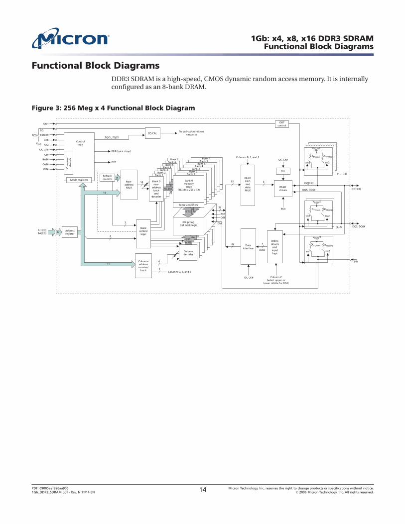
Functional Block DiagramsDDR3 SDRAM is a high-speed, CMOS dynamic random access memory. It is internallyconfigured as an 8-bank DRAM.
Figure 3: 256 Meg x 4 Functional Block Diagram
Bank 5Bank 6
Bank 7
Bank 4
Bank 7
Bank 4Bank 5
Bank 6
14
Row-address
MUX
Controllogic
Column-addresscounter/
latch
Mode registers
11
Co
mm
and
d
eco
de
A[13:0]BA[2:0]
14
Addressregister
17
256(x32)
8,192
I/O gatingDM mask logic
Columndecoder
Bank 0memory
array(16,384 x 256 x 32)
Bank 0row-
addresslatchand
decoder
16,384
Sense amplifiers
Bankcontrollogic
16
Bank 1Bank 2
Bank 3
14
8
3
3
Refreshcounter
4
32
32
32
DQS, DQS#
Columns 0, 1, and 2
Columns 0, 1, and 2
ZQCL, ZQCS
To pull-up/pull-downnetworks
READ drivers DQ[3:0]
READFIFOanddataMUX
Data
4
3
Bank 1Bank 2
Bank 3
DM
DM
CK, CK#
DQS, DQS#
ZQ CAL
CS#
ZQ
RZQ
CK, CK#
RAS#
WE#
CAS#
ODT
CKE
RESET#
CK, CK#
DLL
DQ[3:0]
(1 . . . 4)
(1, 2)
sw1 sw2
VDDQ/2
RTT,nom RTT(WR)
sw1 sw2
VDDQ/2
RTT,nom RTT(WR)
sw1 sw2
VDDQ/2
RTT,nom RTT(WR)
OTF
BC4 (burst chop)
BC4
Column 2(select upper or
lower nibble for BC4)
Datainterface
WRITE driversand inputlogic
ODTcontrol
VSSQ A12
OTF
BC4
1Gb: x4, x8, x16 DDR3 SDRAMFunctional Block Diagrams
PDF: 09005aef826aa9061Gb_DDR3_SDRAM.pdf - Rev. N 11/14 EN 14 Micron Technology, Inc. reserves the right to change products or specifications without notice.
© 2006 Micron Technology, Inc. All rights reserved.
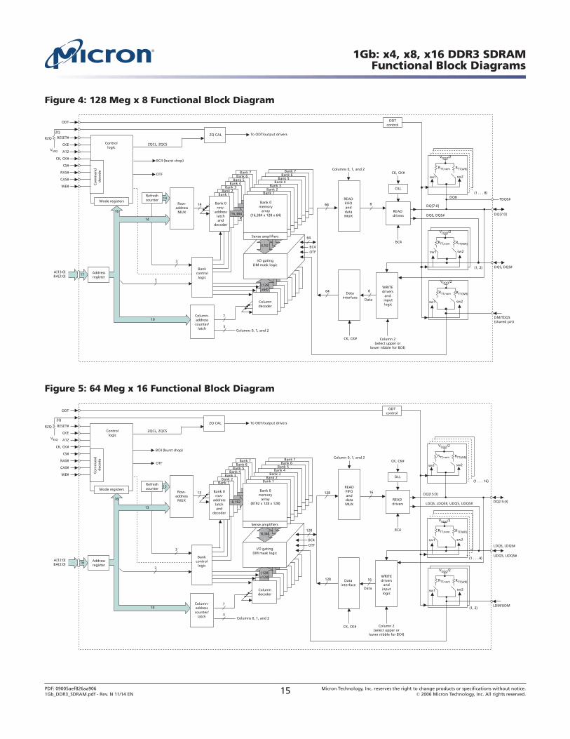
Figure 4: 128 Meg x 8 Functional Block Diagram
Bank 5Bank 6
Bank 7
Bank 4
Bank 7
Bank 4Bank 5
Bank 6
14
Row-address
MUX
Controllogic
Column-addresscounter/
latch
Mode registers
10
Co
mm
and
d
eco
de
A[13:0]BA[2:0]
14
Addressregister
17
8,192
I/O gatingDM mask logic
Columndecoder
Bank 0memory
array(16,384 x 128 x 64)
Bank 0row-
addresslatchand
decoder
16,384
Sense amplifiers
Bankcontrol
logic
16
Bank 1Bank 2
Bank 3
14
7
3
3
Refreshcounter
8
64
64
64
DQS, DQS#
Columns 0, 1, and 2
Columns 0, 1, and 2
ZQCL, ZQCS
To ODT/output drivers
READ drivers DQ[7:0]
READFIFOanddataMUX
Data
8
3
Bank 1Bank 2
Bank 3
DM/TDQS(shared pin)
TDQS#
CK, CK#
DQS, DQS#
ZQ CALZQ
RZQ
CK, CK#
RAS#
WE#
CAS#
CS#
ODT
CKE
RESET#
CK, CK#
DLL
DQ[7:0]
DQ8(1 . . . 8)
(1, 2)
sw1 sw2
VDDQ/2
RTT,nom RTT(WR)
sw1 sw2
VDDQ/2
RTT,nom RTT(WR)
sw1 sw2
VDDQ/2
RTT,nom RTT(WR)
BC4 (burst chop)
BC4BC4
WRITE drivers
and input logic
Datainterface
Column 2(select upper or
lower nibble for BC4)
(128x64)
ODTcontrol
VSSQ A12
OTF
OTF
Figure 5: 64 Meg x 16 Functional Block Diagram
Bank 5Bank 6
Bank 7
Bank 4
Bank 7
Bank 4Bank 5
Bank 6
13
Row-address
MUX
Controllogic
Column-addresscounter/
latch
Mode registers
10
Co
mm
and
d
eco
de
A[12:0]BA[2:0]
13
Addressregister
16
(128x128)
16,384
I/O gatingDM mask logic
Columndecoder
Bank 0memory
array(8192 x 128 x 128)
Bank 0row-
addresslatchand
decoder
8,192
Sense amplifiers
Bankcontrollogic
16
Bank 1Bank 2
Bank 3
13
7
3
3
Refreshcounter
16
128
128
128
LDQS, LDQS#, UDQS, UDQS#
Column 0, 1, and 2
Columns 0, 1, and 2
ZQCL, ZQCS
To ODT/output drivers
BC4
READ drivers
DQ[15:0]
READFIFOanddataMUX
Data
16
BC4 (burst chop)
3
Bank 1Bank 2
Bank 3
LDM/UDM
CK, CK#
LDQS, LDQS#
UDQS, UDQS#
ZQ CALZQ
RZQ
ODT
CKE
CK, CK#
RAS#
WE#
CAS#
CS#
RESET#
CK, CK#
DLL
DQ[15:0]
(1 . . . 16)
(1 . . . 4)
(1, 2)
sw1 sw2
VDDQ/2
RTT,nom RTT(WR)
BC4
sw1 sw2
VDDQ/2
RTT,nom RTT(WR)
sw1 sw2
VDDQ/2
RTT,nom RTT(WR)
Column 2(select upper or
lower nibble for BC4)
Datainterface
WRITE drivers
andinputlogic
ODTcontrol
VSSQ A12
OTF
OTF
1Gb: x4, x8, x16 DDR3 SDRAMFunctional Block Diagrams
PDF: 09005aef826aa9061Gb_DDR3_SDRAM.pdf - Rev. N 11/14 EN 15 Micron Technology, Inc. reserves the right to change products or specifications without notice.
© 2006 Micron Technology, Inc. All rights reserved.
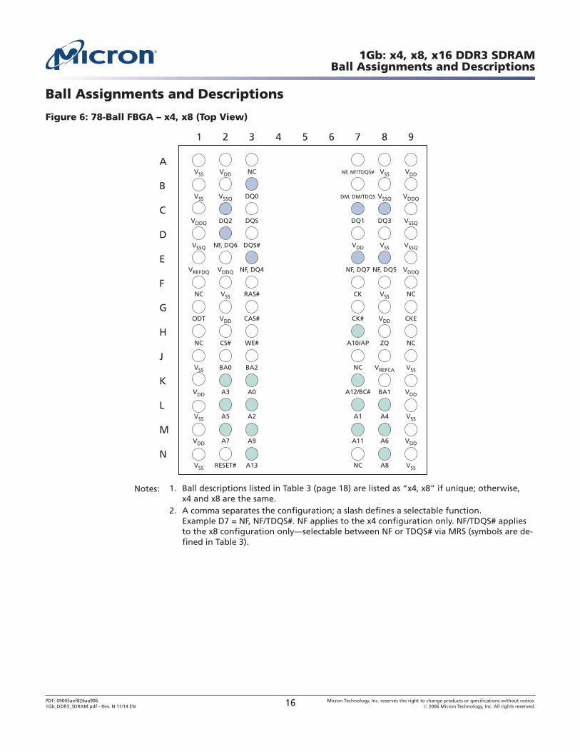
Ball Assignments and Descriptions
Figure 6: 78-Ball FBGA – x4, x8 (Top View)
1 2 3 4 6 7 8 95
VSS
VSS
VDDQ
VSSQ
VREFDQ
NC
ODT
NC
VSS
VDD
VSS
VDD
VSS
VDD
VSSQ
DQ2
NF, DQ6
VDDQ
VSS
VDD
CS#
BA0
A3
A5
A7
RESET#
NC
DQ0
DQS
DQS#
NF, DQ4
RAS#
CAS#
WE#
BA2
A0
A2
A9
A13
NF, NF/TDQS#
DM, DM/TDQS
DQ1
VDD
NF, DQ7
CK
CK#
A10/AP
NC
A12/BC#
A1
A11
NC
VDD
VDDQ
VSSQ
VSSQ
VDDQ
NC
CKE
NC
VSS
VDD
VSS
VDD
VSS
VSS
VSSQ
DQ3
VSS
NF, DQ5
VSS
VDD
ZQ
VREFCA
BA1
A4
A6
A8
A
B
C
D
E
F
G
H
J
K
L
M
N
Notes: 1. Ball descriptions listed in Table 3 (page 18) are listed as “x4, x8” if unique; otherwise,x4 and x8 are the same.
2. A comma separates the configuration; a slash defines a selectable function.Example D7 = NF, NF/TDQS#. NF applies to the x4 configuration only. NF/TDQS# appliesto the x8 configuration only—selectable between NF or TDQS# via MRS (symbols are de-fined in Table 3).
1Gb: x4, x8, x16 DDR3 SDRAMBall Assignments and Descriptions
PDF: 09005aef826aa9061Gb_DDR3_SDRAM.pdf - Rev. N 11/14 EN 16 Micron Technology, Inc. reserves the right to change products or specifications without notice.
© 2006 Micron Technology, Inc. All rights reserved.
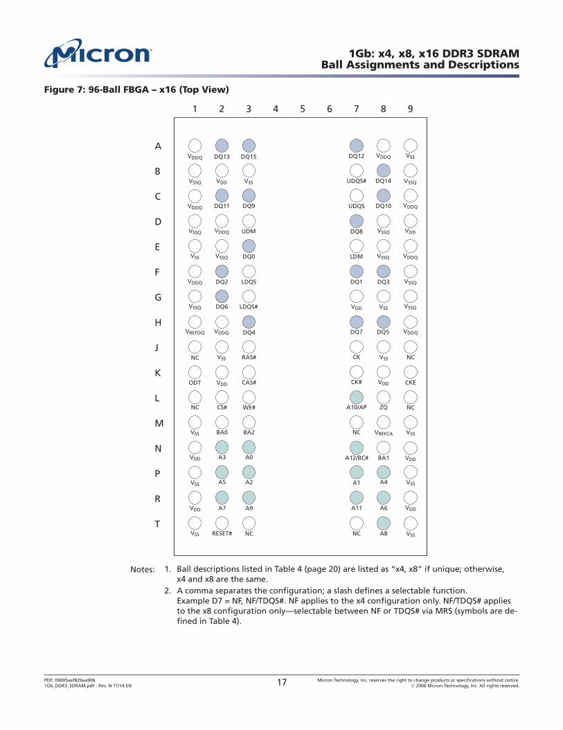
Figure 7: 96-Ball FBGA – x16 (Top View)
1 2 3 4 6 7 8 95
A
B
C
D
E
F
G
H
J
K
L
M
N
P
R
TVSS
VDD
VSS
VSS
NC CS#
BA0
A3
A5
A7
RESET#
NC VSS
VREFDQ VDDQ DQ4
RAS#
CAS#
WE#
BA2
A0
A2
A9
NC
VSSQ
VSSQ
VSSQ VDD VSS
VDDQ DQ2 LDQS
DQ6 LDQS#
VDDQ
VDDQ DQ13 DQ15
DQ11 DQ9
VDDQ UDM
VSS VSSQ DQ0
ODT VDD
VDD
NC
A11
A1
NC
A10/AP ZQ
VREFCA
BA1
A4
A6
A8
CK VSS
DQ7 DQ5 VDDQ
NC
CKE
NC
VSS
VDD
VSS
VDD
VSS
VDD
DQ8
UDQS# DQ14 VSSQ
DQ1 DQ3 VSSQ
VSS VSSQ
UDQS
DQ12 VDDQ VSS
DQ10 VDDQ
VSSQ VDD
LDM VSSQ VDDQ
CK# VDD
A12/BC#
Notes: 1. Ball descriptions listed in Table 4 (page 20) are listed as “x4, x8” if unique; otherwise,x4 and x8 are the same.
2. A comma separates the configuration; a slash defines a selectable function.Example D7 = NF, NF/TDQS#. NF applies to the x4 configuration only. NF/TDQS# appliesto the x8 configuration only—selectable between NF or TDQS# via MRS (symbols are de-fined in Table 4).
1Gb: x4, x8, x16 DDR3 SDRAMBall Assignments and Descriptions
PDF: 09005aef826aa9061Gb_DDR3_SDRAM.pdf - Rev. N 11/14 EN 17 Micron Technology, Inc. reserves the right to change products or specifications without notice.
© 2006 Micron Technology, Inc. All rights reserved.
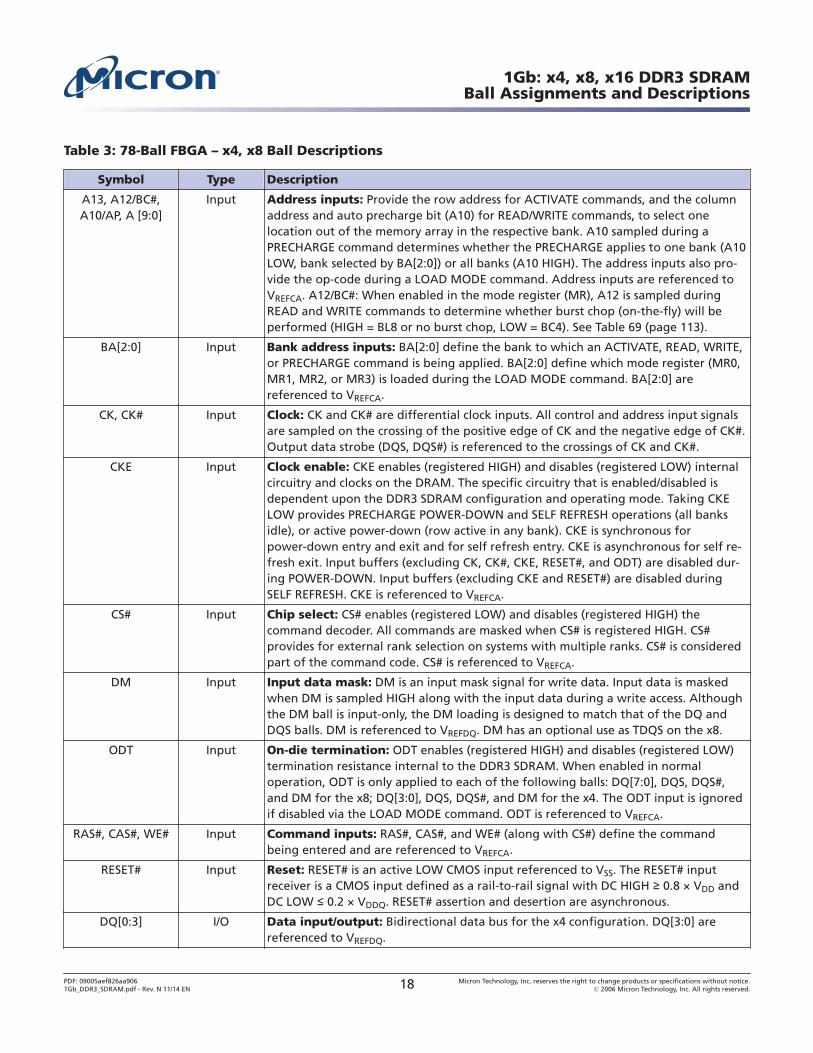
Table 3: 78-Ball FBGA – x4, x8 Ball Descriptions
Symbol Type Description
A13, A12/BC#,A10/AP, A [9:0]
Input Address inputs: Provide the row address for ACTIVATE commands, and the columnaddress and auto precharge bit (A10) for READ/WRITE commands, to select onelocation out of the memory array in the respective bank. A10 sampled during aPRECHARGE command determines whether the PRECHARGE applies to one bank (A10LOW, bank selected by BA[2:0]) or all banks (A10 HIGH). The address inputs also pro-vide the op-code during a LOAD MODE command. Address inputs are referenced toVREFCA. A12/BC#: When enabled in the mode register (MR), A12 is sampled duringREAD and WRITE commands to determine whether burst chop (on-the-fly) will beperformed (HIGH = BL8 or no burst chop, LOW = BC4). See Table 69 (page 113).
BA[2:0] Input Bank address inputs: BA[2:0] define the bank to which an ACTIVATE, READ, WRITE,or PRECHARGE command is being applied. BA[2:0] define which mode register (MR0,MR1, MR2, or MR3) is loaded during the LOAD MODE command. BA[2:0] arereferenced to VREFCA.
CK, CK# Input Clock: CK and CK# are differential clock inputs. All control and address input signalsare sampled on the crossing of the positive edge of CK and the negative edge of CK#.Output data strobe (DQS, DQS#) is referenced to the crossings of CK and CK#.
CKE Input Clock enable: CKE enables (registered HIGH) and disables (registered LOW) internalcircuitry and clocks on the DRAM. The specific circuitry that is enabled/disabled isdependent upon the DDR3 SDRAM configuration and operating mode. Taking CKELOW provides PRECHARGE POWER-DOWN and SELF REFRESH operations (all banksidle), or active power-down (row active in any bank). CKE is synchronous forpower-down entry and exit and for self refresh entry. CKE is asynchronous for self re-fresh exit. Input buffers (excluding CK, CK#, CKE, RESET#, and ODT) are disabled dur-ing POWER-DOWN. Input buffers (excluding CKE and RESET#) are disabled duringSELF REFRESH. CKE is referenced to VREFCA.
CS# Input Chip select: CS# enables (registered LOW) and disables (registered HIGH) thecommand decoder. All commands are masked when CS# is registered HIGH. CS#provides for external rank selection on systems with multiple ranks. CS# is consideredpart of the command code. CS# is referenced to VREFCA.
DM Input Input data mask: DM is an input mask signal for write data. Input data is maskedwhen DM is sampled HIGH along with the input data during a write access. Althoughthe DM ball is input-only, the DM loading is designed to match that of the DQ andDQS balls. DM is referenced to VREFDQ. DM has an optional use as TDQS on the x8.
ODT Input On-die termination: ODT enables (registered HIGH) and disables (registered LOW)termination resistance internal to the DDR3 SDRAM. When enabled in normaloperation, ODT is only applied to each of the following balls: DQ[7:0], DQS, DQS#,and DM for the x8; DQ[3:0], DQS, DQS#, and DM for the x4. The ODT input is ignoredif disabled via the LOAD MODE command. ODT is referenced to VREFCA.
RAS#, CAS#, WE# Input Command inputs: RAS#, CAS#, and WE# (along with CS#) define the commandbeing entered and are referenced to VREFCA.
RESET# Input Reset: RESET# is an active LOW CMOS input referenced to VSS. The RESET# inputreceiver is a CMOS input defined as a rail-to-rail signal with DC HIGH ≥ 0.8 × VDD andDC LOW ≤ 0.2 × VDDQ. RESET# assertion and desertion are asynchronous.
DQ[0:3] I/O Data input/output: Bidirectional data bus for the x4 configuration. DQ[3:0] arereferenced to VREFDQ.
1Gb: x4, x8, x16 DDR3 SDRAMBall Assignments and Descriptions
PDF: 09005aef826aa9061Gb_DDR3_SDRAM.pdf - Rev. N 11/14 EN 18 Micron Technology, Inc. reserves the right to change products or specifications without notice.
© 2006 Micron Technology, Inc. All rights reserved.
Table 3: 78-Ball FBGA – x4, x8 Ball Descriptions (Continued)
Symbol Type Description
DQ[0:7] I/O Data input/output: Bidirectional data bus for the x8 configuration. DQ[7:0] arereferenced to VREFDQ.
DQS, DQS# I/O Data strobe: Output with read data. Edge-aligned with read data. Input with writedata. Center-aligned to write data.
TDQS, TDQS# Output Termination data strobe: Applies to the x8 configuration only. When TDQS isenabled, DM is disabled, and the TDQS and TDQS# balls provide termination resist-ance.
VDD Supply Power supply: 1.5V ±0.075V.
VDDQ Supply DQ power supply: 1.5V ±0.075V. Isolated on the device for improved noise immuni-ty.
VREFCA Supply Reference voltage for control, command, and address: VREFCA must bemaintained at all times (including self refresh) for proper device operation.
VREFDQ Supply Reference voltage for data: VREFDQ must be maintained at all times (excluding selfrefresh) for proper device operation.
VSS Supply Ground.
VSSQ Supply DQ ground: Isolated on the device for improved noise immunity.
ZQ Reference External reference ball for output drive calibration: This ball is tied to anexternal 240Ω resistor (RZQ), which is tied to VSSQ.
NC – No connect: These balls should be left unconnected (the ball has no connection tothe DRAM or to other balls).
NF – No function: When configured as a x4 device, these balls are NF. When configured asa x8 device, these balls are defined as TDQS#, DQ[7:4].
1Gb: x4, x8, x16 DDR3 SDRAMBall Assignments and Descriptions
PDF: 09005aef826aa9061Gb_DDR3_SDRAM.pdf - Rev. N 11/14 EN 19 Micron Technology, Inc. reserves the right to change products or specifications without notice.
© 2006 Micron Technology, Inc. All rights reserved.
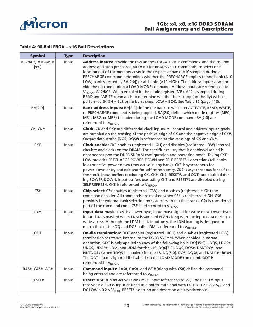
Table 4: 96-Ball FBGA – x16 Ball Descriptions
Symbol Type Description
A12/BC#, A10/AP, A[9:0]
Input Address inputs: Provide the row address for ACTIVATE commands, and the columnaddress and auto precharge bit (A10) for READ/WRITE commands, to select onelocation out of the memory array in the respective bank. A10 sampled during aPRECHARGE command determines whether the PRECHARGE applies to one bank (A10LOW, bank selected by BA[2:0]) or all banks (A10 HIGH). The address inputs also pro-vide the op-code during a LOAD MODE command. Address inputs are referenced toVREFCA. A12/BC#: When enabled in the mode register (MR), A12 is sampled duringREAD and WRITE commands to determine whether burst chop (on-the-fly) will beperformed (HIGH = BL8 or no burst chop, LOW = BC4). See Table 69 (page 113).
BA[2:0] Input Bank address inputs: BA[2:0] define the bank to which an ACTIVATE, READ, WRITE,or PRECHARGE command is being applied. BA[2:0] define which mode register (MR0,MR1, MR2, or MR3) is loaded during the LOAD MODE command. BA[2:0] arereferenced to VREFCA.
CK, CK# Input Clock: CK and CK# are differential clock inputs. All control and address input signalsare sampled on the crossing of the positive edge of CK and the negative edge of CK#.Output data strobe (DQS, DQS#) is referenced to the crossings of CK and CK#.
CKE Input Clock enable: CKE enables (registered HIGH) and disables (registered LOW) internalcircuitry and clocks on the DRAM. The specific circuitry that is enabled/disabled isdependent upon the DDR3 SDRAM configuration and operating mode. Taking CKELOW provides PRECHARGE POWER-DOWN and SELF REFRESH operations (all banksidle),or active power-down (row active in any bank). CKE is synchronous forpower-down entry and exit and for self refresh entry. CKE is asynchronous for self re-fresh exit. Input buffers (excluding CK, CK#, CKE, RESET#, and ODT) are disabled dur-ing POWER-DOWN. Input buffers (excluding CKE and RESET#) are disabled duringSELF REFRESH. CKE is referenced to VREFCA.
CS# Input Chip select: CS# enables (registered LOW) and disables (registered HIGH) thecommand decoder. All commands are masked when CS# is registered HIGH. CS#provides for external rank selection on systems with multiple ranks. CS# is consideredpart of the command code. CS# is referenced to VREFCA.
LDM Input Input data mask: LDM is a lower-byte, input mask signal for write data. Lower-byteinput data is masked when LDM is sampled HIGH along with the input data during awrite access. Although the LDM ball is input-only, the LDM loading is designed tomatch that of the DQ and DQS balls. LDM is referenced to VREFDQ.
ODT Input On-die termination: ODT enables (registered HIGH) and disables (registered LOW)termination resistance internal to the DDR3 SDRAM. When enabled in normaloperation, ODT is only applied to each of the following balls: DQ[15:0], LDQS, LDQS#,UDQS, UDQS#, LDM, and UDM for the x16; DQ0[7:0], DQS, DQS#, DM/TDQS, andNF/TDQS# (when TDQS is enabled) for the x8; DQ[3:0], DQS, DQS#, and DM for the x4.The ODT input is ignored if disabled via the LOAD MODE command. ODT isreferenced to VREFCA.
RAS#, CAS#, WE# Input Command inputs: RAS#, CAS#, and WE# (along with CS#) define the commandbeing entered and are referenced to VREFCA.
RESET# Input Reset: RESET# is an active LOW CMOS input referenced to VSS. The RESET# inputreceiver is a CMOS input defined as a rail-to-rail signal with DC HIGH ≥ 0.8 × VDD andDC LOW ≤ 0.2 × VDDQ. RESET# assertion and desertion are asynchronous.
1Gb: x4, x8, x16 DDR3 SDRAMBall Assignments and Descriptions
PDF: 09005aef826aa9061Gb_DDR3_SDRAM.pdf - Rev. N 11/14 EN 20 Micron Technology, Inc. reserves the right to change products or specifications without notice.
© 2006 Micron Technology, Inc. All rights reserved.
Table 4: 96-Ball FBGA – x16 Ball Descriptions (Continued)
Symbol Type Description
UDM Input Input data mask: UDM is an upper-byte, input mask signal for write data. Upper-byte input data is masked when UDM is sampled HIGH along with that input dataduring a WRITE access. Although the UDM ball is input-only, the UDM loading isdesigned to match that of the DQ and DQS balls. UDM is referenced to VREFDQ.
DQ[0:7] I/O Data input/output: Lower byte of bidirectional data bus for the x16 configuration.DQ[7:0] are referenced to VREFDQ.
DQ[8:15] I/O Data input/output: Upper byte of bidirectional data bus for the x16 configuration.DQ[15:8] are referenced to VREFDQ.
LDQS, LDQS# I/O Lower byte data strobe: Output with read data. Edge-aligned with read data.Input with write data. Center-aligned to write data.
UDQS, UDQS# I/O Upper byte data strobe: Output with read data. Edge-aligned with read data.Input with write data. DQS is center-aligned to write data.
VDD Supply Power supply: 1.5V ±0.075V.
VDDQ Supply DQ power supply: 1.5V ±0.075V. Isolated on the device for improved noise immuni-ty.
VREFCA Supply Reference voltage for control, command, and address: VREFCA must bemaintained at all times (including self refresh) for proper device operation.
VREFDQ Supply Reference voltage for data: VREFDQ must be maintained at all times (excluding selfrefresh) for proper device operation.
VSS Supply Ground.
VSSQ Supply DQ ground: Isolated on the device for improved noise immunity.
ZQ Reference External reference ball for output drive calibration: This ball is tied to anexternal 240Ω resistor (RZQ), which is tied to VSSQ.
NC – No connect: These balls should be left unconnected (the ball has no connection tothe DRAM or to other balls).
1Gb: x4, x8, x16 DDR3 SDRAMBall Assignments and Descriptions
PDF: 09005aef826aa9061Gb_DDR3_SDRAM.pdf - Rev. N 11/14 EN 21 Micron Technology, Inc. reserves the right to change products or specifications without notice.
© 2006 Micron Technology, Inc. All rights reserved.
Package Dimensions
Figure 8: 78-Ball FBGA – x4, x8 (JP)
Ball A1 ID
1.2 MAX0.8TYP
0.8 ±0.1Seating
plane
A
9.6CTR
6.4 CTR
0.12 A
78X Ø0.45
11.5 ±0.15
Ball A1 ID
0.8 TYP
8 ±0.15
0.25 MIN
9 8 7 3 2 1
A
B
C
D
E
F
G
H
J
K
L
M
N
Dimensions applyto solder balls post-
reflow on Ø0.33NSMD ball pads.
Notes: 1. All dimensions are in millimeters.2. Material composition: Pb-free SAC305 (96.5% Sn, 3% Ag, 0.5% Cu).
1Gb: x4, x8, x16 DDR3 SDRAMPackage Dimensions
PDF: 09005aef826aa9061Gb_DDR3_SDRAM.pdf - Rev. N 11/14 EN 22 Micron Technology, Inc. reserves the right to change products or specifications without notice.
© 2006 Micron Technology, Inc. All rights reserved.
Figure 9: 78-Ball FBGA – x4, x8 (DA)
1.8 CTRNonconductive
overmold
0.155
Seating plane
0.12 A
Ball A1 ID(covered by SR)
Ball A1 ID
0.29 MIN
1.1 ±0.1
6.4 CTR
8 ±0.1
0.8 TYP
9.6 CTR
10.5 ±0.1
78X Ø0.47Dimensions applyto solder balls post-reflow on Ø0.42 SMDball pads.
0.8 TYP
123789
ABCDEFGHJKLMN
A
Notes: 1. All dimensions are in millimeters.2. Material composition: Pb-free SAC302 (96.8% Sn, 3% Ag, 0.2% Cu).
1Gb: x4, x8, x16 DDR3 SDRAMPackage Dimensions
PDF: 09005aef826aa9061Gb_DDR3_SDRAM.pdf - Rev. N 11/14 EN 23 Micron Technology, Inc. reserves the right to change products or specifications without notice.
© 2006 Micron Technology, Inc. All rights reserved.
Figure 10: 96-Ball FBGA – x16 (JT)
Seating plane
0.12 A
123789
A
B
C
D
E
F
G
H
J
K
L
M
N
Ball A1 ID Ball A1 ID
A
0.25 MIN
1.1 ±0.10.8 TYP
6.4 CTR
8 ±0.1
0.8 TYP
12 CTR
14 ±0.1
96X Ø0.45Dimensions applyto solder balls post-reflow on Ø0.35SMD ball pads.
0.155
P
R
T
1.8 CTRNonconductive
overmold
Notes: 1. All dimensions are in millimeters.2. Material composition: Pb-free SAC305 (96.5% Sn, 3% Ag, 0.5% Cu).
1Gb: x4, x8, x16 DDR3 SDRAMPackage Dimensions
PDF: 09005aef826aa9061Gb_DDR3_SDRAM.pdf - Rev. N 11/14 EN 24 Micron Technology, Inc. reserves the right to change products or specifications without notice.
© 2006 Micron Technology, Inc. All rights reserved.
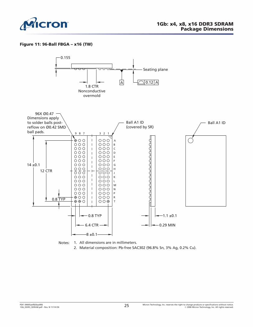
Figure 11: 96-Ball FBGA – x16 (TW)
1.8 CTRNonconductive
overmold
0.155
Seating plane
0.12 A
Ball A1 ID(covered by SR)
Ball A1 ID
0.29 MIN
1.1 ±0.1
6.4 CTR
8 ±0.1
0.8 TYP
12 CTR
14 ±0.1
96X Ø0.47Dimensions applyto solder balls post-reflow on Ø0.42 SMDball pads.
0.8 TYP
123789
ABCDEFGHJKLMNPRT
A
Notes: 1. All dimensions are in millimeters.2. Material composition: Pb-free SAC302 (96.8% Sn, 3% Ag, 0.2% Cu).
1Gb: x4, x8, x16 DDR3 SDRAMPackage Dimensions
PDF: 09005aef826aa9061Gb_DDR3_SDRAM.pdf - Rev. N 11/14 EN 25 Micron Technology, Inc. reserves the right to change products or specifications without notice.
© 2006 Micron Technology, Inc. All rights reserved.
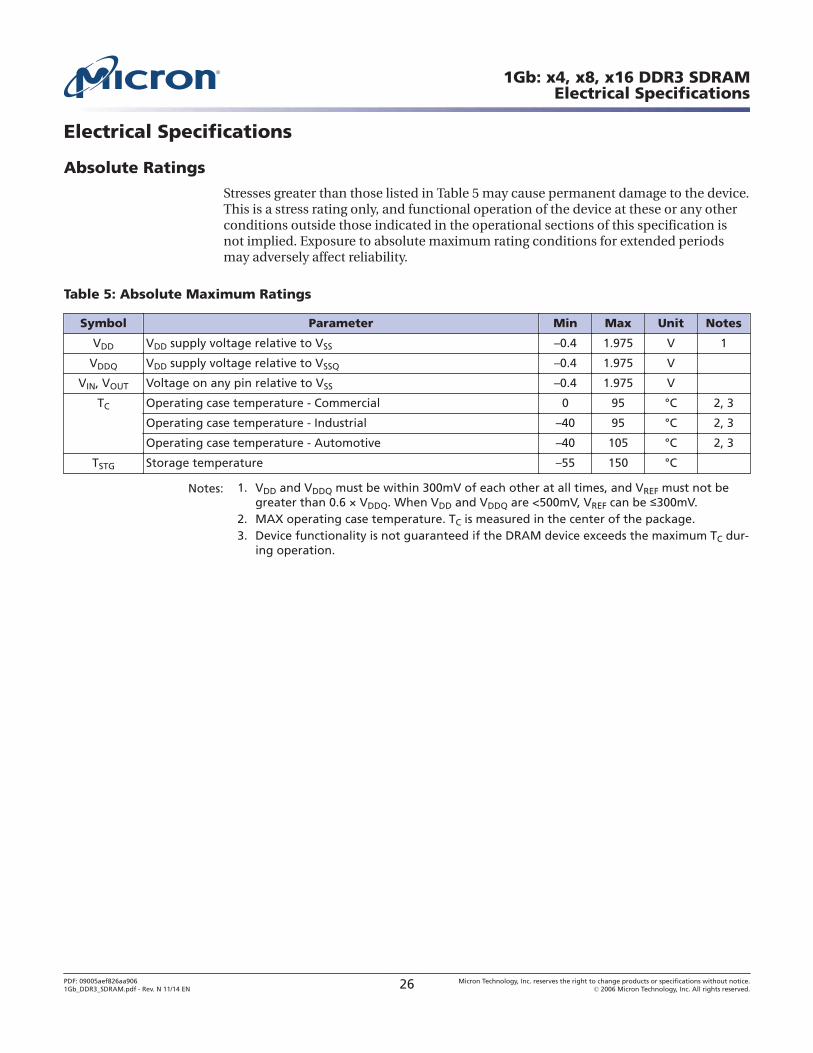
Electrical Specifications
Absolute Ratings
Stresses greater than those listed in Table 5 may cause permanent damage to the device.This is a stress rating only, and functional operation of the device at these or any otherconditions outside those indicated in the operational sections of this specification isnot implied. Exposure to absolute maximum rating conditions for extended periodsmay adversely affect reliability.
Table 5: Absolute Maximum Ratings
Symbol Parameter Min Max Unit Notes
VDD VDD supply voltage relative to VSS –0.4 1.975 V 1
VDDQ VDD supply voltage relative to VSSQ –0.4 1.975 V
VIN, VOUT Voltage on any pin relative to VSS –0.4 1.975 V
TC Operating case temperature - Commercial 0 95 °C 2, 3
Operating case temperature - Industrial –40 95 °C 2, 3
Operating case temperature - Automotive –40 105 °C 2, 3
TSTG Storage temperature –55 150 °C
Notes: 1. VDD and VDDQ must be within 300mV of each other at all times, and VREF must not begreater than 0.6 × VDDQ. When VDD and VDDQ are <500mV, VREF can be ≤300mV.
2. MAX operating case temperature. TC is measured in the center of the package.3. Device functionality is not guaranteed if the DRAM device exceeds the maximum TC dur-
ing operation.
1Gb: x4, x8, x16 DDR3 SDRAMElectrical Specifications
PDF: 09005aef826aa9061Gb_DDR3_SDRAM.pdf - Rev. N 11/14 EN 26 Micron Technology, Inc. reserves the right to change products or specifications without notice.
© 2006 Micron Technology, Inc. All rights reserved.
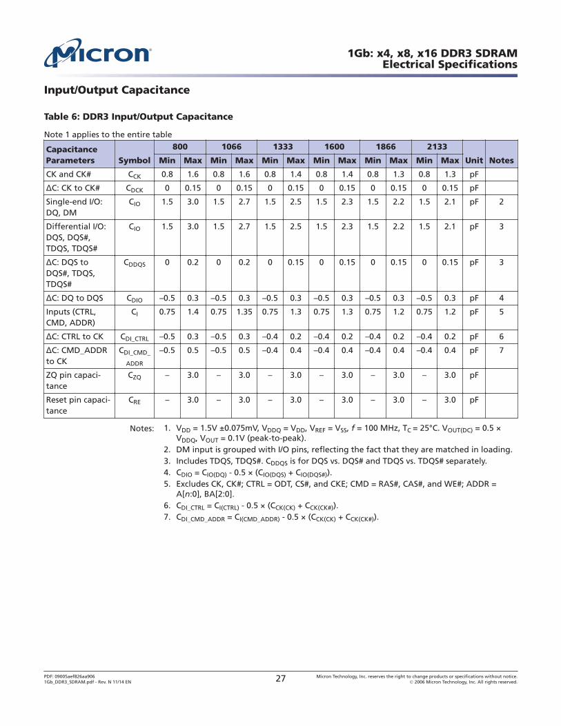
Input/Output Capacitance
Table 6: DDR3 Input/Output Capacitance
Note 1 applies to the entire table
CapacitanceParameters Symbol
800 1066 1333 1600 1866 2133
Unit NotesMin Max Min Max Min Max Min Max Min Max Min Max
CK and CK# CCK 0.8 1.6 0.8 1.6 0.8 1.4 0.8 1.4 0.8 1.3 0.8 1.3 pF
ΔC: CK to CK# CDCK 0 0.15 0 0.15 0 0.15 0 0.15 0 0.15 0 0.15 pF
Single-end I/O:DQ, DM
CIO 1.5 3.0 1.5 2.7 1.5 2.5 1.5 2.3 1.5 2.2 1.5 2.1 pF 2
Differential I/O:DQS, DQS#,TDQS, TDQS#
CIO 1.5 3.0 1.5 2.7 1.5 2.5 1.5 2.3 1.5 2.2 1.5 2.1 pF 3
ΔC: DQS toDQS#, TDQS,TDQS#
CDDQS 0 0.2 0 0.2 0 0.15 0 0.15 0 0.15 0 0.15 pF 3
ΔC: DQ to DQS CDIO –0.5 0.3 –0.5 0.3 –0.5 0.3 –0.5 0.3 –0.5 0.3 –0.5 0.3 pF 4
Inputs (CTRL,CMD, ADDR)
CI 0.75 1.4 0.75 1.35 0.75 1.3 0.75 1.3 0.75 1.2 0.75 1.2 pF 5
ΔC: CTRL to CK CDI_CTRL –0.5 0.3 –0.5 0.3 –0.4 0.2 –0.4 0.2 –0.4 0.2 –0.4 0.2 pF 6
ΔC: CMD_ADDRto CK
CDI_CMD_
ADDR
–0.5 0.5 –0.5 0.5 –0.4 0.4 –0.4 0.4 –0.4 0.4 –0.4 0.4 pF 7
ZQ pin capaci-tance
CZQ – 3.0 – 3.0 – 3.0 – 3.0 – 3.0 – 3.0 pF
Reset pin capaci-tance
CRE – 3.0 – 3.0 – 3.0 – 3.0 – 3.0 – 3.0 pF
Notes: 1. VDD = 1.5V ±0.075mV, VDDQ = VDD, VREF = VSS, f = 100 MHz, TC = 25°C. VOUT(DC) = 0.5 ×VDDQ, VOUT = 0.1V (peak-to-peak).
2. DM input is grouped with I/O pins, reflecting the fact that they are matched in loading.3. Includes TDQS, TDQS#. CDDQS is for DQS vs. DQS# and TDQS vs. TDQS# separately.4. CDIO = CIO(DQ) - 0.5 × (CIO(DQS) + CIO(DQS#)).5. Excludes CK, CK#; CTRL = ODT, CS#, and CKE; CMD = RAS#, CAS#, and WE#; ADDR =
A[n:0], BA[2:0].6. CDI_CTRL = CI(CTRL) - 0.5 × (CCK(CK) + CCK(CK#)).7. CDI_CMD_ADDR = CI(CMD_ADDR) - 0.5 × (CCK(CK) + CCK(CK#)).
1Gb: x4, x8, x16 DDR3 SDRAMElectrical Specifications
PDF: 09005aef826aa9061Gb_DDR3_SDRAM.pdf - Rev. N 11/14 EN 27 Micron Technology, Inc. reserves the right to change products or specifications without notice.
© 2006 Micron Technology, Inc. All rights reserved.
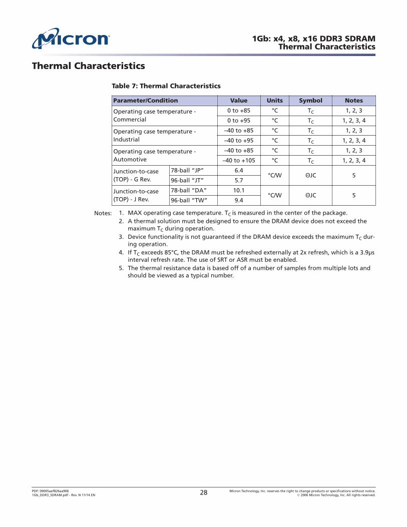
Thermal Characteristics
Table 7: Thermal Characteristics
Parameter/Condition Value Units Symbol Notes
Operating case temperature -Commercial
0 to +85 °C TC 1, 2, 3
0 to +95 °C TC 1, 2, 3, 4
Operating case temperature -Industrial
–40 to +85 °C TC 1, 2, 3
–40 to +95 °C TC 1, 2, 3, 4
Operating case temperature -Automotive
–40 to +85 °C TC 1, 2, 3
–40 to +105 °C TC 1, 2, 3, 4
Junction-to-case(TOP) - G Rev.
78-ball “JP” 6.4°C/W ΘJC 5
96-ball “JT” 5.7
Junction-to-case(TOP) - J Rev.
78-ball “DA” 10.1°C/W ΘJC 5
96-ball “TW” 9.4
Notes: 1. MAX operating case temperature. TC is measured in the center of the package.2. A thermal solution must be designed to ensure the DRAM device does not exceed the
maximum TC during operation.3. Device functionality is not guaranteed if the DRAM device exceeds the maximum TC dur-
ing operation.4. If TC exceeds 85°C, the DRAM must be refreshed externally at 2x refresh, which is a 3.9μs
interval refresh rate. The use of SRT or ASR must be enabled.5. The thermal resistance data is based off of a number of samples from multiple lots and
should be viewed as a typical number.
1Gb: x4, x8, x16 DDR3 SDRAMThermal Characteristics
PDF: 09005aef826aa9061Gb_DDR3_SDRAM.pdf - Rev. N 11/14 EN 28 Micron Technology, Inc. reserves the right to change products or specifications without notice.
© 2006 Micron Technology, Inc. All rights reserved.
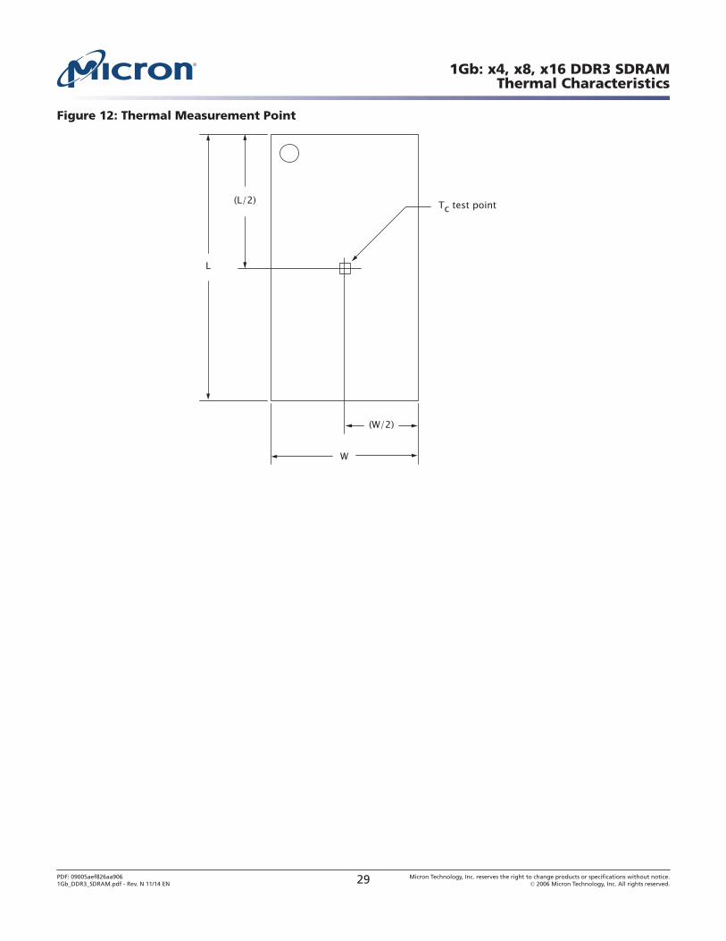
Figure 12: Thermal Measurement Point
(L/2)
L
W
(W/2)
Tc test point
1Gb: x4, x8, x16 DDR3 SDRAMThermal Characteristics
PDF: 09005aef826aa9061Gb_DDR3_SDRAM.pdf - Rev. N 11/14 EN 29 Micron Technology, Inc. reserves the right to change products or specifications without notice.
© 2006 Micron Technology, Inc. All rights reserved.
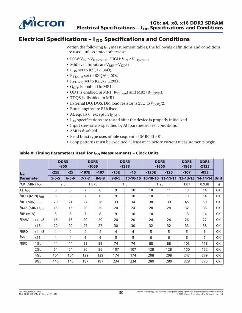
Electrical Specifications – I DD Specifications and ConditionsWithin the following IDD measurement tables, the following definitions and conditionsare used, unless stated otherwise:
• LOW: VIN ≤ VIL(AC)max; HIGH: VIN ≥ VIH(AC)min.• Midlevel: Inputs are VREF = VDD/2.• RON set to RZQ/7 (34Ω• RTT,nom set to RZQ/6 (40Ω• RTT(WR) set to RZQ/2 (120Ω• QOFF is enabled in MR1.• ODT is enabled in MR1 (RTT,nom) and MR2 (RTT(WR)).• TDQS is disabled in MR1.• External DQ/DQS/DM load resistor is 25Ω to VDDQ/2.• Burst lengths are BL8 fixed.• AL equals 0 (except in IDD7).• IDD specifications are tested after the device is properly initialized.• Input slew rate is specified by AC parametric test conditions.• ASR is disabled.• Read burst type uses nibble sequential (MR0[3] = 0).• Loop patterns must be executed at least once before current measurements begin.
Table 8: Timing Parameters Used for IDD Measurements – Clock Units
IDD
Parameter
DDR3-800
DDR3-1066
DDR3-1333
DDR3-1600
DDR3-1866
DDR3-2133
Unit
-25E -25 -187E -187 -15E -15 -125E -125 -107 -093
5-5-5 6-6-6 7-7-7 8-8-8 9-9-9 10-10-10 10-10-10 11-11-11 13-13-13 14-14-14tCK (MIN) IDD 2.5 1.875 1.5 1.25 1.07 0.938 ns
CL IDD 5 6 7 8 9 10 10 11 13 14 CKtRCD (MIN) IDD 5 6 7 8 9 10 10 11 13 14 CKtRC (MIN) IDD 20 21 27 28 33 34 38 39 45 50 CKtRAS (MIN) IDD 15 15 20 20 24 24 28 28 32 36 CKtRP (MIN) 5 6 7 8 9 10 10 11 13 14 CKtFAW x4, x8 16 16 20 20 20 20 24 24 26 27 CK
x16 20 20 27 27 30 30 32 32 33 38 CKtRRDIDD
x4, x8 4 4 4 4 4 4 5 5 5 6 CK
x16 4 4 6 6 5 5 6 6 6 7 CKtRFC 1Gb 44 44 59 59 74 74 88 88 103 118 CK
2Gb 64 64 86 86 107 107 128 128 150 172 CK
4Gb 104 104 139 139 174 174 208 208 243 279 CK
8Gb 140 140 187 187 234 234 280 280 328 375 CK
1Gb: x4, x8, x16 DDR3 SDRAMElectrical Specifications – I DD Specifications and Conditions
PDF: 09005aef826aa9061Gb_DDR3_SDRAM.pdf - Rev. N 11/14 EN 30 Micron Technology, Inc. reserves the right to change products or specifications without notice.
© 2006 Micron Technology, Inc. All rights reserved.
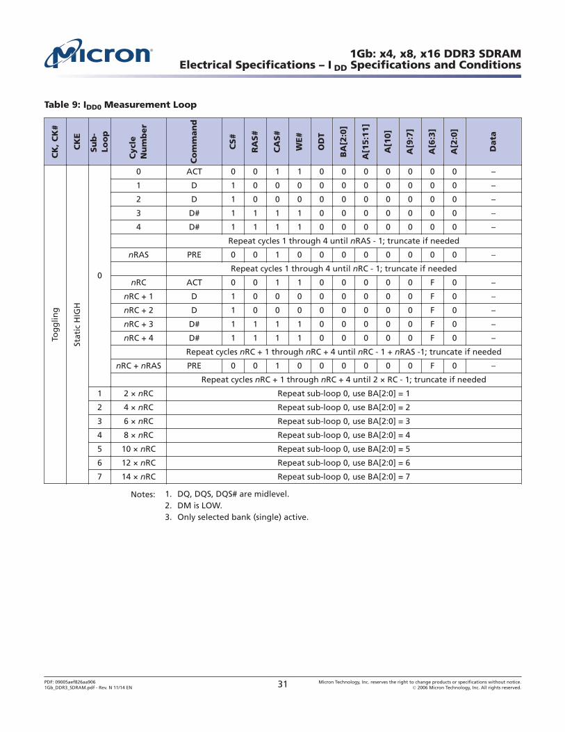
Table 9: IDD0 Measurement Loop
CK
, C
K#
CK
E
Su
b-
Loo
p
Cycl
eN
um
ber
Co
mm
an
d
CS#
RA
S#
CA
S#
WE#
OD
T
BA
[2:0
]
A[1
5:1
1]
A[1
0]
A[9
:7]
A[6
:3]
A[2
:0]
Data
Tog
glin
g
Stat
ic H
IGH
0
0 ACT 0 0 1 1 0 0 0 0 0 0 0 –
1 D 1 0 0 0 0 0 0 0 0 0 0 –
2 D 1 0 0 0 0 0 0 0 0 0 0 –
3 D# 1 1 1 1 0 0 0 0 0 0 0 –
4 D# 1 1 1 1 0 0 0 0 0 0 0 –
Repeat cycles 1 through 4 until nRAS - 1; truncate if needed
nRAS PRE 0 0 1 0 0 0 0 0 0 0 0 –
Repeat cycles 1 through 4 until nRC - 1; truncate if needed
nRC ACT 0 0 1 1 0 0 0 0 0 F 0 –
nRC + 1 D 1 0 0 0 0 0 0 0 0 F 0 –
nRC + 2 D 1 0 0 0 0 0 0 0 0 F 0 –
nRC + 3 D# 1 1 1 1 0 0 0 0 0 F 0 –
nRC + 4 D# 1 1 1 1 0 0 0 0 0 F 0 –
Repeat cycles nRC + 1 through nRC + 4 until nRC - 1 + nRAS -1; truncate if needed
nRC + nRAS PRE 0 0 1 0 0 0 0 0 0 F 0 –
Repeat cycles nRC + 1 through nRC + 4 until 2 × RC - 1; truncate if needed
1 2 × nRC Repeat sub-loop 0, use BA[2:0] = 1
2 4 × nRC Repeat sub-loop 0, use BA[2:0] = 2
3 6 × nRC Repeat sub-loop 0, use BA[2:0] = 3
4 8 × nRC Repeat sub-loop 0, use BA[2:0] = 4
5 10 × nRC Repeat sub-loop 0, use BA[2:0] = 5
6 12 × nRC Repeat sub-loop 0, use BA[2:0] = 6
7 14 × nRC Repeat sub-loop 0, use BA[2:0] = 7
Notes: 1. DQ, DQS, DQS# are midlevel.2. DM is LOW.3. Only selected bank (single) active.
1Gb: x4, x8, x16 DDR3 SDRAMElectrical Specifications – I DD Specifications and Conditions
PDF: 09005aef826aa9061Gb_DDR3_SDRAM.pdf - Rev. N 11/14 EN 31 Micron Technology, Inc. reserves the right to change products or specifications without notice.
© 2006 Micron Technology, Inc. All rights reserved.
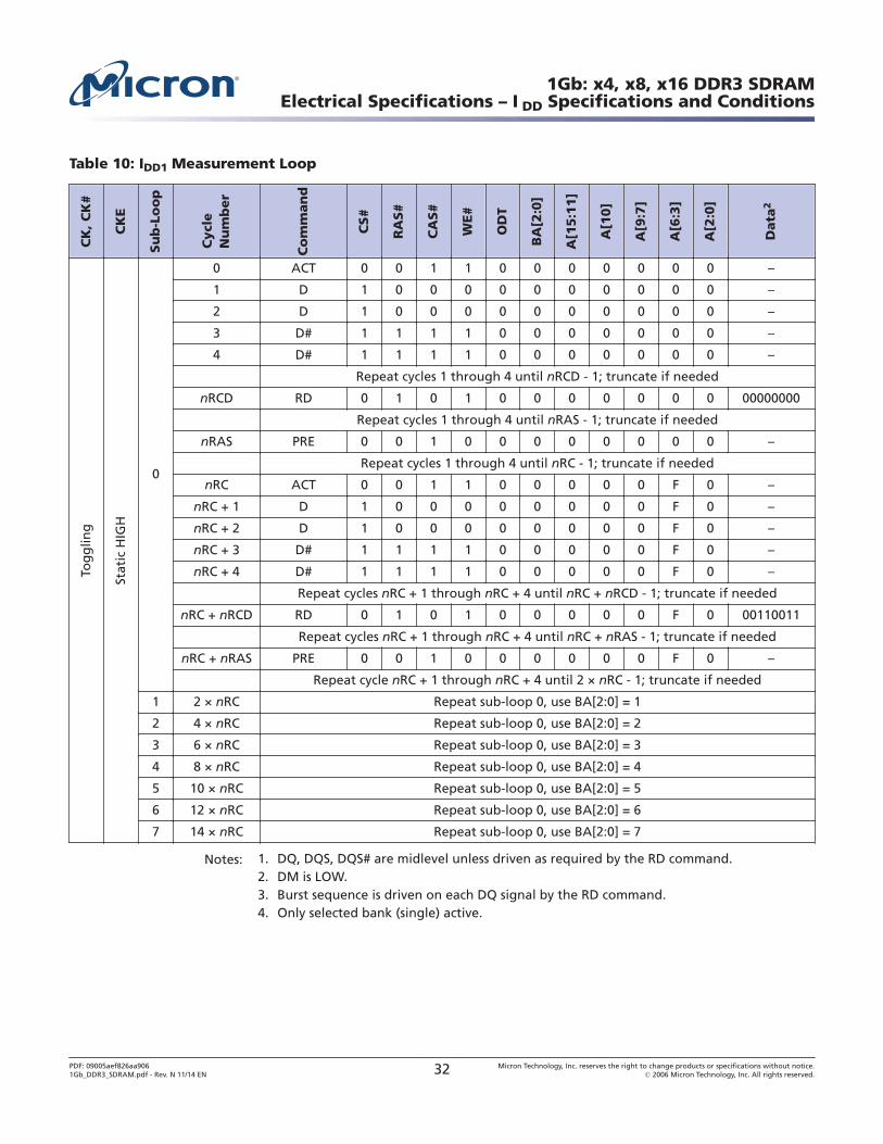
Table 10: IDD1 Measurement Loop
CK
, C
K#
CK
E
Su
b-L
oo
p
Cycl
eN
um
ber
Co
mm
an
d
CS#
RA
S#
CA
S#
WE#
OD
T
BA
[2:0
]
A[1
5:1
1]
A[1
0]
A[9
:7]
A[6
:3]
A[2
:0]
Data
2
Tog
glin
g
Stat
ic H
IGH
0
0 ACT 0 0 1 1 0 0 0 0 0 0 0 –
1 D 1 0 0 0 0 0 0 0 0 0 0 –
2 D 1 0 0 0 0 0 0 0 0 0 0 –
3 D# 1 1 1 1 0 0 0 0 0 0 0 –
4 D# 1 1 1 1 0 0 0 0 0 0 0 –
Repeat cycles 1 through 4 until nRCD - 1; truncate if needed
nRCD RD 0 1 0 1 0 0 0 0 0 0 0 00000000
Repeat cycles 1 through 4 until nRAS - 1; truncate if needed
nRAS PRE 0 0 1 0 0 0 0 0 0 0 0 –
Repeat cycles 1 through 4 until nRC - 1; truncate if needed
nRC ACT 0 0 1 1 0 0 0 0 0 F 0 –
nRC + 1 D 1 0 0 0 0 0 0 0 0 F 0 –
nRC + 2 D 1 0 0 0 0 0 0 0 0 F 0 –
nRC + 3 D# 1 1 1 1 0 0 0 0 0 F 0 –
nRC + 4 D# 1 1 1 1 0 0 0 0 0 F 0 –
Repeat cycles nRC + 1 through nRC + 4 until nRC + nRCD - 1; truncate if needed
nRC + nRCD RD 0 1 0 1 0 0 0 0 0 F 0 00110011
Repeat cycles nRC + 1 through nRC + 4 until nRC + nRAS - 1; truncate if needed
nRC + nRAS PRE 0 0 1 0 0 0 0 0 0 F 0 –
Repeat cycle nRC + 1 through nRC + 4 until 2 × nRC - 1; truncate if needed
1 2 × nRC Repeat sub-loop 0, use BA[2:0] = 1
2 4 × nRC Repeat sub-loop 0, use BA[2:0] = 2
3 6 × nRC Repeat sub-loop 0, use BA[2:0] = 3
4 8 × nRC Repeat sub-loop 0, use BA[2:0] = 4
5 10 × nRC Repeat sub-loop 0, use BA[2:0] = 5
6 12 × nRC Repeat sub-loop 0, use BA[2:0] = 6
7 14 × nRC Repeat sub-loop 0, use BA[2:0] = 7
Notes: 1. DQ, DQS, DQS# are midlevel unless driven as required by the RD command.2. DM is LOW.3. Burst sequence is driven on each DQ signal by the RD command.4. Only selected bank (single) active.
1Gb: x4, x8, x16 DDR3 SDRAMElectrical Specifications – I DD Specifications and Conditions
PDF: 09005aef826aa9061Gb_DDR3_SDRAM.pdf - Rev. N 11/14 EN 32 Micron Technology, Inc. reserves the right to change products or specifications without notice.
© 2006 Micron Technology, Inc. All rights reserved.
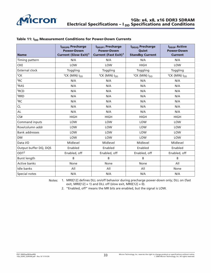
Table 11: IDD Measurement Conditions for Power-Down Currents
Name
IDD2P0 PrechargePower-Down
Current (Slow Exit)1
IDD2P1 PrechargePower-Down
Current (Fast Exit)1
IDD2Q PrechargeQuiet
Standby Current
IDD3P ActivePower-Down
Current
Timing pattern N/A N/A N/A N/A
CKE LOW LOW HIGH LOW
External clock Toggling Toggling Toggling TogglingtCK tCK (MIN) IDD
tCK (MIN) IDDtCK (MIN) IDD
tCK (MIN) IDD
tRC N/A N/A N/A N/AtRAS N/A N/A N/A N/AtRCD N/A N/A N/A N/AtRRD N/A N/A N/A N/AtRC N/A N/A N/A N/A
CL N/A N/A N/A N/A
AL N/A N/A N/A N/A
CS# HIGH HIGH HIGH HIGH
Command inputs LOW LOW LOW LOW
Row/column addr LOW LOW LOW LOW
Bank addresses LOW LOW LOW LOW
DM LOW LOW LOW LOW
Data I/O Midlevel Midlevel Midlevel Midlevel
Output buffer DQ, DQS Enabled Enabled Enabled Enabled
ODT2 Enabled, off Enabled, off Enabled, off Enabled, off
Burst length 8 8 8 8
Active banks None None None All
Idle banks All All All None
Special notes N/A N/A N/A N/A
Notes: 1. MR0[12] defines DLL on/off behavior during precharge power-down only; DLL on (fastexit, MR0[12] = 1) and DLL off (slow exit, MR0[12] = 0).
2. “Enabled, off” means the MR bits are enabled, but the signal is LOW.
1Gb: x4, x8, x16 DDR3 SDRAMElectrical Specifications – I DD Specifications and Conditions
PDF: 09005aef826aa9061Gb_DDR3_SDRAM.pdf - Rev. N 11/14 EN 33 Micron Technology, Inc. reserves the right to change products or specifications without notice.
© 2006 Micron Technology, Inc. All rights reserved.
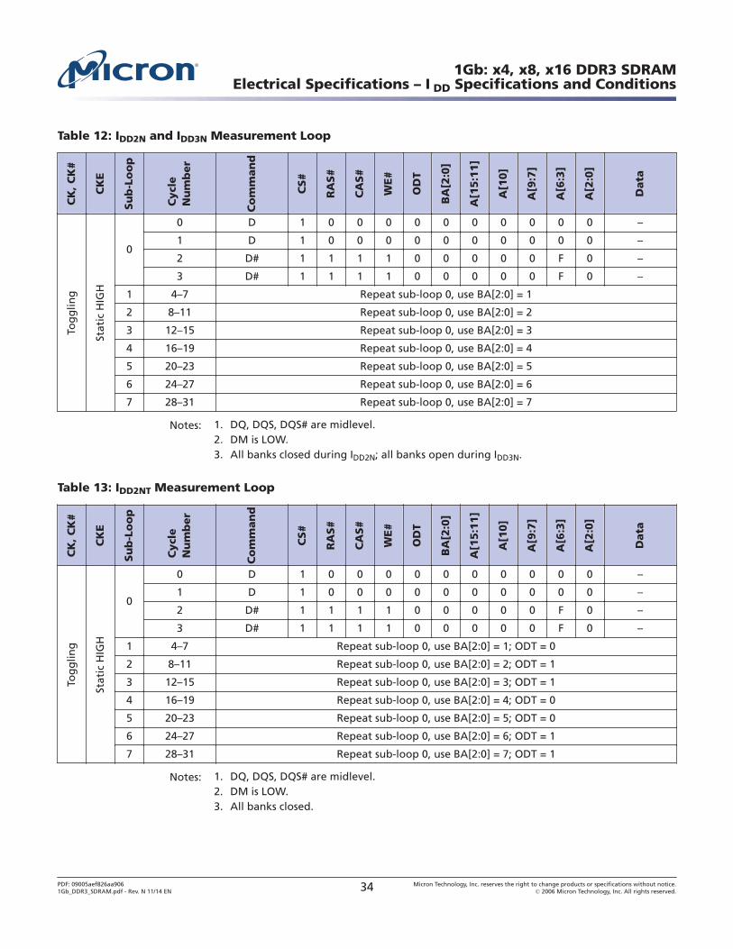
Table 12: IDD2N and IDD3N Measurement Loop
CK
, C
K#
CK
E
Su
b-L
oo
p
Cycl
eN
um
ber
Co
mm
an
d
CS#
RA
S#
CA
S#
WE#
OD
T
BA
[2:0
]
A[1
5:1
1]
A[1
0]
A[9
:7]
A[6
:3]
A[2
:0]
Data
Tog
glin
g
Stat
ic H
IGH
0
0 D 1 0 0 0 0 0 0 0 0 0 0 –
1 D 1 0 0 0 0 0 0 0 0 0 0 –
2 D# 1 1 1 1 0 0 0 0 0 F 0 –
3 D# 1 1 1 1 0 0 0 0 0 F 0 –
1 4–7 Repeat sub-loop 0, use BA[2:0] = 1
2 8–11 Repeat sub-loop 0, use BA[2:0] = 2
3 12–15 Repeat sub-loop 0, use BA[2:0] = 3
4 16–19 Repeat sub-loop 0, use BA[2:0] = 4
5 20–23 Repeat sub-loop 0, use BA[2:0] = 5
6 24–27 Repeat sub-loop 0, use BA[2:0] = 6
7 28–31 Repeat sub-loop 0, use BA[2:0] = 7
Notes: 1. DQ, DQS, DQS# are midlevel.2. DM is LOW.3. All banks closed during IDD2N; all banks open during IDD3N.
Table 13: IDD2NT Measurement Loop
CK
, C
K#
CK
E
Su
b-L
oo
p
Cycl
eN
um
ber
Co
mm
an
d
CS#
RA
S#
CA
S#
WE#
OD
T
BA
[2:0
]
A[1
5:1
1]
A[1
0]
A[9
:7]
A[6
:3]
A[2
:0]
Data
Tog
glin
g
Stat
ic H
IGH
0
0 D 1 0 0 0 0 0 0 0 0 0 0 –
1 D 1 0 0 0 0 0 0 0 0 0 0 –
2 D# 1 1 1 1 0 0 0 0 0 F 0 –
3 D# 1 1 1 1 0 0 0 0 0 F 0 –
1 4–7 Repeat sub-loop 0, use BA[2:0] = 1; ODT = 0
2 8–11 Repeat sub-loop 0, use BA[2:0] = 2; ODT = 1
3 12–15 Repeat sub-loop 0, use BA[2:0] = 3; ODT = 1
4 16–19 Repeat sub-loop 0, use BA[2:0] = 4; ODT = 0
5 20–23 Repeat sub-loop 0, use BA[2:0] = 5; ODT = 0
6 24–27 Repeat sub-loop 0, use BA[2:0] = 6; ODT = 1
7 28–31 Repeat sub-loop 0, use BA[2:0] = 7; ODT = 1
Notes: 1. DQ, DQS, DQS# are midlevel.2. DM is LOW.3. All banks closed.
1Gb: x4, x8, x16 DDR3 SDRAMElectrical Specifications – I DD Specifications and Conditions
PDF: 09005aef826aa9061Gb_DDR3_SDRAM.pdf - Rev. N 11/14 EN 34 Micron Technology, Inc. reserves the right to change products or specifications without notice.
© 2006 Micron Technology, Inc. All rights reserved.

Table 14: IDD4R Measurement Loop
CK
, C
K#
CK
E
Su
b-L
oo
p
Cycl
eN
um
ber
Co
mm
an
d
CS#
RA
S#
CA
S#
WE#
OD
T
BA
[2:0
]
A[1
5:1
1]
A[1
0]
A[9
:7]
A[6
:3]
A[2
:0]
Data
3
Tog
glin
g
Stat
ic H
IGH
0
0 RD 0 1 0 1 0 0 0 0 0 0 0 00000000
1 D 1 0 0 0 0 0 0 0 0 0 0 –
2 D# 1 1 1 1 0 0 0 0 0 0 0 –
3 D# 1 1 1 1 0 0 0 0 0 0 0 –
4 RD 0 1 0 1 0 0 0 0 0 F 0 00110011
5 D 1 0 0 0 0 0 0 0 0 F 0 –
6 D# 1 1 1 1 0 0 0 0 0 F 0 –
7 D# 1 1 1 1 0 0 0 0 0 F 0 –
1 8–15 Repeat sub-loop 0, use BA[2:0] = 1
2 16–23 Repeat sub-loop 0, use BA[2:0] = 2
3 24–31 Repeat sub-loop 0, use BA[2:0] = 3
4 32–39 Repeat sub-loop 0, use BA[2:0] = 4
5 40–47 Repeat sub-loop 0, use BA[2:0] = 5
6 48–55 Repeat sub-loop 0, use BA[2:0] = 6
7 56–63 Repeat sub-loop 0, use BA[2:0] = 7
Notes: 1. DQ, DQS, DQS# are midlevel when not driving in burst sequence.2. DM is LOW.3. Burst sequence is driven on each DQ signal by the RD command.4. All banks open.
1Gb: x4, x8, x16 DDR3 SDRAMElectrical Specifications – I DD Specifications and Conditions
PDF: 09005aef826aa9061Gb_DDR3_SDRAM.pdf - Rev. N 11/14 EN 35 Micron Technology, Inc. reserves the right to change products or specifications without notice.
© 2006 Micron Technology, Inc. All rights reserved.
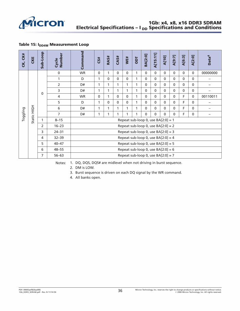
Table 15: IDD4W Measurement Loop
CK
, C
K#
CK
E
Su
b-L
oo
p
Cycl
eN
um
ber
Co
mm
an
d
CS#
RA
S#
CA
S#
WE#
OD
T
BA
[2:0
]
A[1
5:1
1]
A[1
0]
A[9
:7]
A[6
:3]
A[2
:0]
Data
4
Tog
glin
g
Stat
ic H
IGH
0
0 WR 0 1 0 0 1 0 0 0 0 0 0 00000000
1 D 1 0 0 0 1 0 0 0 0 0 0 –
2 D# 1 1 1 1 1 0 0 0 0 0 0 –
3 D# 1 1 1 1 1 0 0 0 0 0 0 –
4 WR 0 1 0 0 1 0 0 0 0 F 0 00110011
5 D 1 0 0 0 1 0 0 0 0 F 0 –
6 D# 1 1 1 1 1 0 0 0 0 F 0 –
7 D# 1 1 1 1 1 0 0 0 0 F 0 –
1 8–15 Repeat sub-loop 0, use BA[2:0] = 1
2 16–23 Repeat sub-loop 0, use BA[2:0] = 2
3 24–31 Repeat sub-loop 0, use BA[2:0] = 3
4 32–39 Repeat sub-loop 0, use BA[2:0] = 4
5 40–47 Repeat sub-loop 0, use BA[2:0] = 5
6 48–55 Repeat sub-loop 0, use BA[2:0] = 6
7 56–63 Repeat sub-loop 0, use BA[2:0] = 7
Notes: 1. DQ, DQS, DQS# are midlevel when not driving in burst sequence.2. DM is LOW.3. Burst sequence is driven on each DQ signal by the WR command.4. All banks open.
1Gb: x4, x8, x16 DDR3 SDRAMElectrical Specifications – I DD Specifications and Conditions
PDF: 09005aef826aa9061Gb_DDR3_SDRAM.pdf - Rev. N 11/14 EN 36 Micron Technology, Inc. reserves the right to change products or specifications without notice.
© 2006 Micron Technology, Inc. All rights reserved.
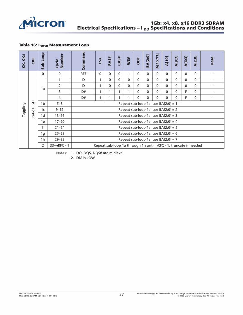
Table 16: IDD5B Measurement Loop
CK
, C
K#
CK
E
Su
b-L
oo
p
Cycl
eN
um
ber
Co
mm
an
d
CS#
RA
S#
CA
S#
WE#
OD
T
BA
[2:0
]
A[1
5:1
1]
A[1
0]
A[9
:7]
A[6
:3]
A[2
:0]
Data
Tog
glin
g
Stat
ic H
IGH
0 0 REF 0 0 0 1 0 0 0 0 0 0 0 –
1a
1 D 1 0 0 0 0 0 0 0 0 0 0 –
2 D 1 0 0 0 0 0 0 0 0 0 0 –
3 D# 1 1 1 1 0 0 0 0 0 F 0 –
4 D# 1 1 1 1 0 0 0 0 0 F 0 –
1b 5–8 Repeat sub-loop 1a, use BA[2:0] = 1
1c 9–12 Repeat sub-loop 1a, use BA[2:0] = 2
1d 13–16 Repeat sub-loop 1a, use BA[2:0] = 3
1e 17–20 Repeat sub-loop 1a, use BA[2:0] = 4
1f 21–24 Repeat sub-loop 1a, use BA[2:0] = 5
1g 25–28 Repeat sub-loop 1a, use BA[2:0] = 6
1h 29–32 Repeat sub-loop 1a, use BA[2:0] = 7
2 33–nRFC - 1 Repeat sub-loop 1a through 1h until nRFC - 1; truncate if needed
Notes: 1. DQ, DQS, DQS# are midlevel.2. DM is LOW.
1Gb: x4, x8, x16 DDR3 SDRAMElectrical Specifications – I DD Specifications and Conditions
PDF: 09005aef826aa9061Gb_DDR3_SDRAM.pdf - Rev. N 11/14 EN 37 Micron Technology, Inc. reserves the right to change products or specifications without notice.
© 2006 Micron Technology, Inc. All rights reserved.
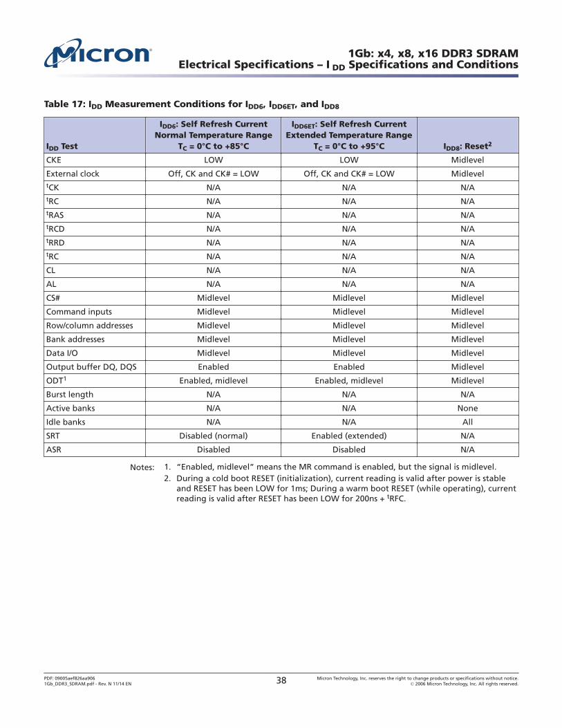
Table 17: IDD Measurement Conditions for IDD6, IDD6ET, and IDD8
IDD Test
IDD6: Self Refresh CurrentNormal Temperature Range
TC = 0°C to +85°C
IDD6ET: Self Refresh CurrentExtended Temperature Range
TC = 0°C to +95°C IDD8: Reset2
CKE LOW LOW Midlevel
External clock Off, CK and CK# = LOW Off, CK and CK# = LOW MidleveltCK N/A N/A N/AtRC N/A N/A N/AtRAS N/A N/A N/AtRCD N/A N/A N/AtRRD N/A N/A N/AtRC N/A N/A N/A
CL N/A N/A N/A
AL N/A N/A N/A
CS# Midlevel Midlevel Midlevel
Command inputs Midlevel Midlevel Midlevel
Row/column addresses Midlevel Midlevel Midlevel
Bank addresses Midlevel Midlevel Midlevel
Data I/O Midlevel Midlevel Midlevel
Output buffer DQ, DQS Enabled Enabled Midlevel
ODT1 Enabled, midlevel Enabled, midlevel Midlevel
Burst length N/A N/A N/A
Active banks N/A N/A None
Idle banks N/A N/A All
SRT Disabled (normal) Enabled (extended) N/A
ASR Disabled Disabled N/A
Notes: 1. “Enabled, midlevel” means the MR command is enabled, but the signal is midlevel.2. During a cold boot RESET (initialization), current reading is valid after power is stable
and RESET has been LOW for 1ms; During a warm boot RESET (while operating), currentreading is valid after RESET has been LOW for 200ns + tRFC.
1Gb: x4, x8, x16 DDR3 SDRAMElectrical Specifications – I DD Specifications and Conditions
PDF: 09005aef826aa9061Gb_DDR3_SDRAM.pdf - Rev. N 11/14 EN 38 Micron Technology, Inc. reserves the right to change products or specifications without notice.
© 2006 Micron Technology, Inc. All rights reserved.
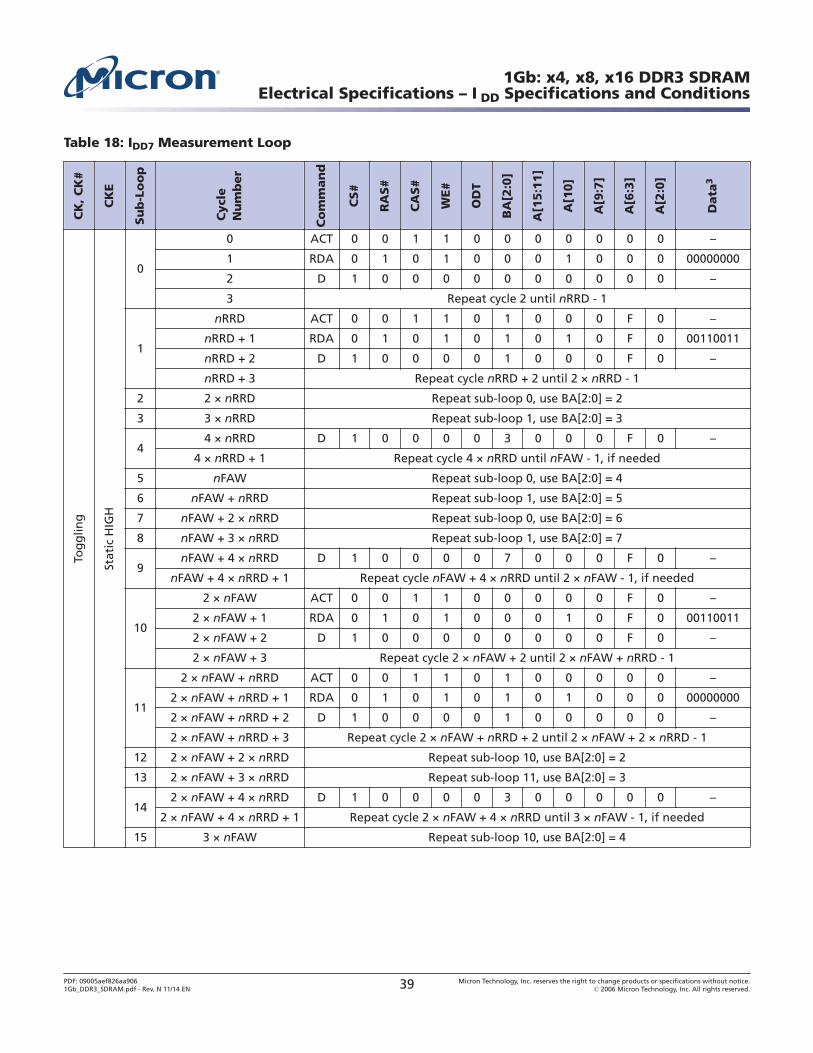
Table 18: IDD7 Measurement Loop
CK
, C
K#
CK
E
Su
b-L
oo
p
Cycl
eN
um
ber
Co
mm
an
d
CS#
RA
S#
CA
S#
WE#
OD
T
BA
[2:0
]
A[1
5:1
1]
A[1
0]
A[9
:7]
A[6
:3]
A[2
:0]
Data
3
Tog
glin
g
Stat
ic H
IGH
0
0 ACT 0 0 1 1 0 0 0 0 0 0 0 –
1 RDA 0 1 0 1 0 0 0 1 0 0 0 00000000
2 D 1 0 0 0 0 0 0 0 0 0 0 –
3 Repeat cycle 2 until nRRD - 1
1
nRRD ACT 0 0 1 1 0 1 0 0 0 F 0 –
nRRD + 1 RDA 0 1 0 1 0 1 0 1 0 F 0 00110011
nRRD + 2 D 1 0 0 0 0 1 0 0 0 F 0 –
nRRD + 3 Repeat cycle nRRD + 2 until 2 × nRRD - 1
2 2 × nRRD Repeat sub-loop 0, use BA[2:0] = 2
3 3 × nRRD Repeat sub-loop 1, use BA[2:0] = 3
44 × nRRD D 1 0 0 0 0 3 0 0 0 F 0 –
4 × nRRD + 1 Repeat cycle 4 × nRRD until nFAW - 1, if needed
5 nFAW Repeat sub-loop 0, use BA[2:0] = 4
6 nFAW + nRRD Repeat sub-loop 1, use BA[2:0] = 5
7 nFAW + 2 × nRRD Repeat sub-loop 0, use BA[2:0] = 6
8 nFAW + 3 × nRRD Repeat sub-loop 1, use BA[2:0] = 7
9nFAW + 4 × nRRD D 1 0 0 0 0 7 0 0 0 F 0 –
nFAW + 4 × nRRD + 1 Repeat cycle nFAW + 4 × nRRD until 2 × nFAW - 1, if needed
10
2 × nFAW ACT 0 0 1 1 0 0 0 0 0 F 0 –
2 × nFAW + 1 RDA 0 1 0 1 0 0 0 1 0 F 0 00110011
2 × nFAW + 2 D 1 0 0 0 0 0 0 0 0 F 0 –
2 × nFAW + 3 Repeat cycle 2 × nFAW + 2 until 2 × nFAW + nRRD - 1
11
2 × nFAW + nRRD ACT 0 0 1 1 0 1 0 0 0 0 0 –
2 × nFAW + nRRD + 1 RDA 0 1 0 1 0 1 0 1 0 0 0 00000000
2 × nFAW + nRRD + 2 D 1 0 0 0 0 1 0 0 0 0 0 –
2 × nFAW + nRRD + 3 Repeat cycle 2 × nFAW + nRRD + 2 until 2 × nFAW + 2 × nRRD - 1
12 2 × nFAW + 2 × nRRD Repeat sub-loop 10, use BA[2:0] = 2
13 2 × nFAW + 3 × nRRD Repeat sub-loop 11, use BA[2:0] = 3
142 × nFAW + 4 × nRRD D 1 0 0 0 0 3 0 0 0 0 0 –
2 × nFAW + 4 × nRRD + 1 Repeat cycle 2 × nFAW + 4 × nRRD until 3 × nFAW - 1, if needed
15 3 × nFAW Repeat sub-loop 10, use BA[2:0] = 4
1Gb: x4, x8, x16 DDR3 SDRAMElectrical Specifications – I DD Specifications and Conditions
PDF: 09005aef826aa9061Gb_DDR3_SDRAM.pdf - Rev. N 11/14 EN 39 Micron Technology, Inc. reserves the right to change products or specifications without notice.
© 2006 Micron Technology, Inc. All rights reserved.
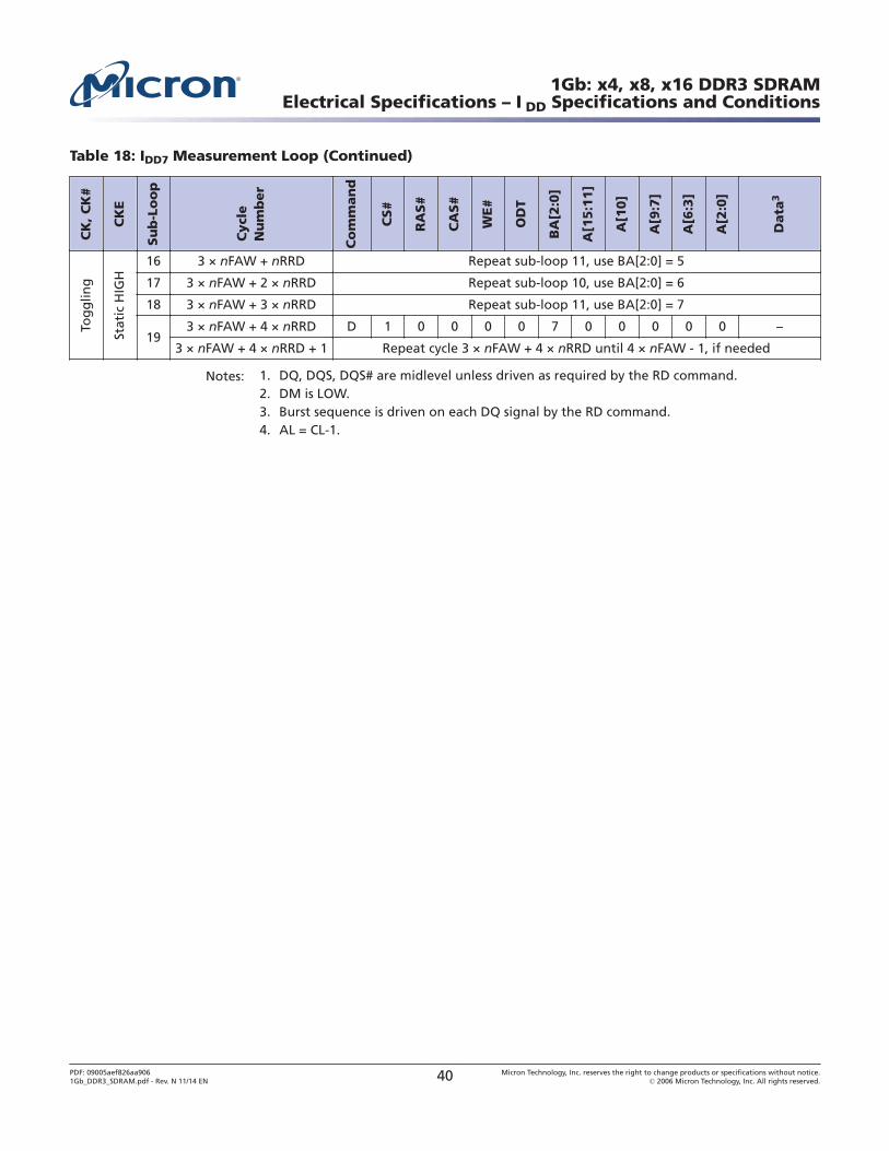
Table 18: IDD7 Measurement Loop (Continued)
CK
, C
K#
CK
E
Su
b-L
oo
p
Cycl
eN
um
ber
Co
mm
an
d
CS#
RA
S#
CA
S#
WE#
OD
T
BA
[2:0
]
A[1
5:1
1]
A[1
0]
A[9
:7]
A[6
:3]
A[2
:0]
Data
3
Tog
glin
g
Stat
ic H
IGH
16 3 × nFAW + nRRD Repeat sub-loop 11, use BA[2:0] = 5
17 3 × nFAW + 2 × nRRD Repeat sub-loop 10, use BA[2:0] = 6
18 3 × nFAW + 3 × nRRD Repeat sub-loop 11, use BA[2:0] = 7
193 × nFAW + 4 × nRRD D 1 0 0 0 0 7 0 0 0 0 0 –
3 × nFAW + 4 × nRRD + 1 Repeat cycle 3 × nFAW + 4 × nRRD until 4 × nFAW - 1, if needed
Notes: 1. DQ, DQS, DQS# are midlevel unless driven as required by the RD command.2. DM is LOW.3. Burst sequence is driven on each DQ signal by the RD command.4. AL = CL-1.
1Gb: x4, x8, x16 DDR3 SDRAMElectrical Specifications – I DD Specifications and Conditions
PDF: 09005aef826aa9061Gb_DDR3_SDRAM.pdf - Rev. N 11/14 EN 40 Micron Technology, Inc. reserves the right to change products or specifications without notice.
© 2006 Micron Technology, Inc. All rights reserved.
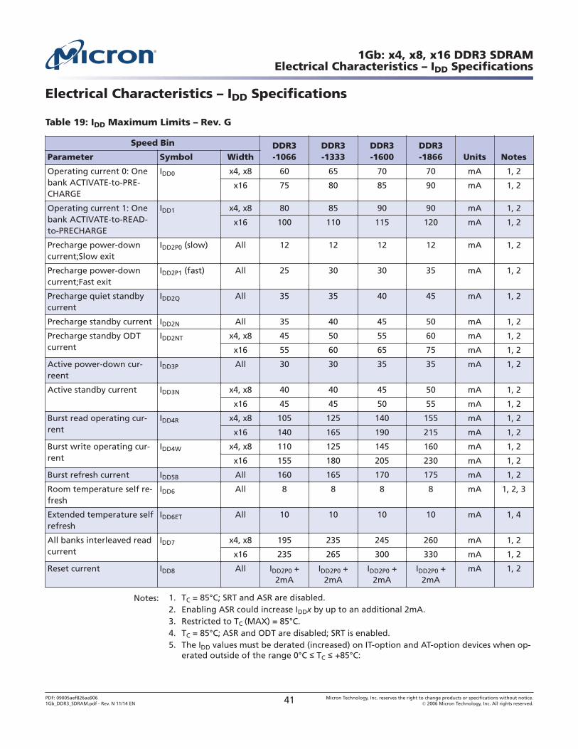
Electrical Characteristics – IDD Specifications
Table 19: IDD Maximum Limits – Rev. G
Speed Bin DDR3-1066
DDR3-1333
DDR3-1600
DDR3-1866 Units NotesParameter Symbol Width
Operating current 0: Onebank ACTIVATE-to-PRE-CHARGE
IDD0 x4, x8 60 65 70 70 mA 1, 2
x16 75 80 85 90 mA 1, 2
Operating current 1: Onebank ACTIVATE-to-READ-to-PRECHARGE
IDD1 x4, x8 80 85 90 90 mA 1, 2
x16 100 110 115 120 mA 1, 2
Precharge power-downcurrent;Slow exit
IDD2P0 (slow) All 12 12 12 12 mA 1, 2
Precharge power-downcurrent;Fast exit
IDD2P1 (fast) All 25 30 30 35 mA 1, 2
Precharge quiet standbycurrent
IDD2Q All 35 35 40 45 mA 1, 2
Precharge standby current IDD2N All 35 40 45 50 mA 1, 2
Precharge standby ODTcurrent
IDD2NT x4, x8 45 50 55 60 mA 1, 2
x16 55 60 65 75 mA 1, 2
Active power-down cur-reent
IDD3P All 30 30 35 35 mA 1, 2
Active standby current IDD3N x4, x8 40 40 45 50 mA 1, 2
x16 45 45 50 55 mA 1, 2
Burst read operating cur-rent
IDD4R x4, x8 105 125 140 155 mA 1, 2
x16 140 165 190 215 mA 1, 2
Burst write operating cur-rent
IDD4W x4, x8 110 125 145 160 mA 1, 2
x16 155 180 205 230 mA 1, 2
Burst refresh current IDD5B All 160 165 170 175 mA 1, 2
Room temperature self re-fresh
IDD6 All 8 8 8 8 mA 1, 2, 3
Extended temperature selfrefresh
IDD6ET All 10 10 10 10 mA 1, 4
All banks interleaved readcurrent
IDD7 x4, x8 195 235 245 260 mA 1, 2
x16 235 265 300 330 mA 1, 2
Reset current IDD8 All IDD2P0 +2mA
IDD2P0 +2mA
IDD2P0 +2mA
IDD2P0 +2mA
mA 1, 2
Notes: 1. TC = 85°C; SRT and ASR are disabled.2. Enabling ASR could increase IDDx by up to an additional 2mA.3. Restricted to TC (MAX) = 85°C.4. TC = 85°C; ASR and ODT are disabled; SRT is enabled.5. The IDD values must be derated (increased) on IT-option and AT-option devices when op-
erated outside of the range 0°C ≤ TC ≤ +85°C:
1Gb: x4, x8, x16 DDR3 SDRAMElectrical Characteristics – IDD Specifications
PDF: 09005aef826aa9061Gb_DDR3_SDRAM.pdf - Rev. N 11/14 EN 41 Micron Technology, Inc. reserves the right to change products or specifications without notice.
© 2006 Micron Technology, Inc. All rights reserved.
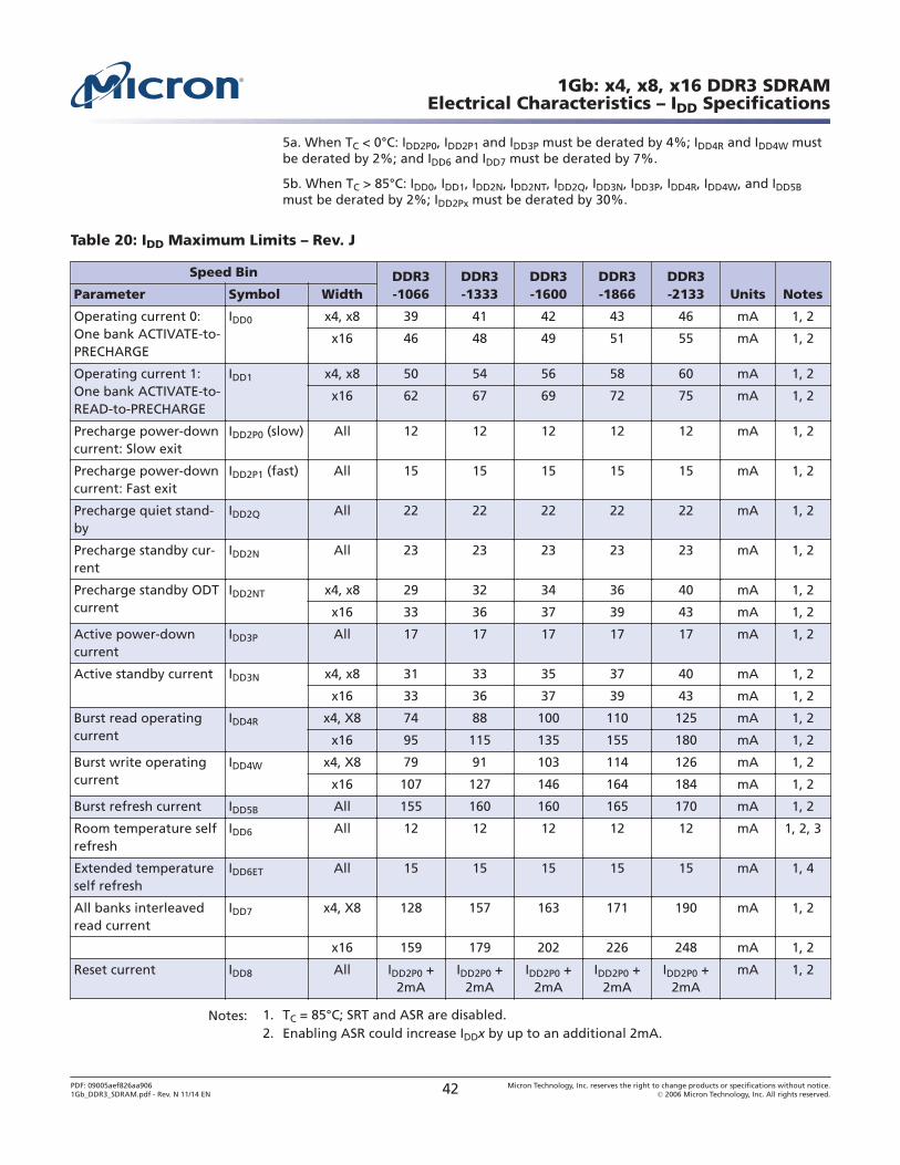
5a. When TC < 0°C: IDD2P0, IDD2P1 and IDD3P must be derated by 4%; IDD4R and IDD4W mustbe derated by 2%; and IDD6 and IDD7 must be derated by 7%.
5b. When TC > 85°C: IDD0, IDD1, IDD2N, IDD2NT, IDD2Q, IDD3N, IDD3P, IDD4R, IDD4W, and IDD5Bmust be derated by 2%; IDD2Px must be derated by 30%.
Table 20: IDD Maximum Limits – Rev. J
Speed Bin DDR3-1066
DDR3-1333
DDR3-1600
DDR3-1866
DDR3-2133 Units NotesParameter Symbol Width
Operating current 0:One bank ACTIVATE-to-PRECHARGE
IDD0 x4, x8 39 41 42 43 46 mA 1, 2
x16 46 48 49 51 55 mA 1, 2
Operating current 1:One bank ACTIVATE-to-READ-to-PRECHARGE
IDD1 x4, x8 50 54 56 58 60 mA 1, 2
x16 62 67 69 72 75 mA 1, 2
Precharge power-downcurrent: Slow exit
IDD2P0 (slow) All 12 12 12 12 12 mA 1, 2
Precharge power-downcurrent: Fast exit
IDD2P1 (fast) All 15 15 15 15 15 mA 1, 2
Precharge quiet stand-by
IDD2Q All 22 22 22 22 22 mA 1, 2
Precharge standby cur-rent
IDD2N All 23 23 23 23 23 mA 1, 2
Precharge standby ODTcurrent
IDD2NT x4, x8 29 32 34 36 40 mA 1, 2
x16 33 36 37 39 43 mA 1, 2
Active power-downcurrent
IDD3P All 17 17 17 17 17 mA 1, 2
Active standby current IDD3N x4, x8 31 33 35 37 40 mA 1, 2
x16 33 36 37 39 43 mA 1, 2
Burst read operatingcurrent
IDD4R x4, X8 74 88 100 110 125 mA 1, 2
x16 95 115 135 155 180 mA 1, 2
Burst write operatingcurrent
IDD4W x4, X8 79 91 103 114 126 mA 1, 2
x16 107 127 146 164 184 mA 1, 2
Burst refresh current IDD5B All 155 160 160 165 170 mA 1, 2
Room temperature selfrefresh
IDD6 All 12 12 12 12 12 mA 1, 2, 3
Extended temperatureself refresh
IDD6ET All 15 15 15 15 15 mA 1, 4
All banks interleavedread current
IDD7 x4, X8 128 157 163 171 190 mA 1, 2
x16 159 179 202 226 248 mA 1, 2
Reset current IDD8 All IDD2P0 +2mA
IDD2P0 +2mA
IDD2P0 +2mA
IDD2P0 +2mA
IDD2P0 +2mA
mA 1, 2
Notes: 1. TC = 85°C; SRT and ASR are disabled.2. Enabling ASR could increase IDDx by up to an additional 2mA.
1Gb: x4, x8, x16 DDR3 SDRAMElectrical Characteristics – IDD Specifications
PDF: 09005aef826aa9061Gb_DDR3_SDRAM.pdf - Rev. N 11/14 EN 42 Micron Technology, Inc. reserves the right to change products or specifications without notice.
© 2006 Micron Technology, Inc. All rights reserved.
3. Restricted to TC (MAX) = 85°C.4. TC = 85°C; ASR and ODT are disabled; SRT is enabled.5. The IDD values must be derated (increased) on IT-option and AT-option devices when op-
erated outside of the range 0°C ≤ TC ≤ +85°C:
5a. When TC < 0°C: IDD2P0, IDD2P1 and IDD3P must be derated by 4%; IDD4R and IDD4W mustbe derated by 2%; and IDD6 and IDD7 must be derated by 7%.
5b. When TC > 85°C: IDD0, IDD1, IDD2N, IDD2NT, IDD2Q, IDD3N, IDD3P, IDD4R, IDD4W, and IDD5Bmust be derated by 2%; IDD2Px must be derated by 30%.
1Gb: x4, x8, x16 DDR3 SDRAMElectrical Characteristics – IDD Specifications
PDF: 09005aef826aa9061Gb_DDR3_SDRAM.pdf - Rev. N 11/14 EN 43 Micron Technology, Inc. reserves the right to change products or specifications without notice.
© 2006 Micron Technology, Inc. All rights reserved.
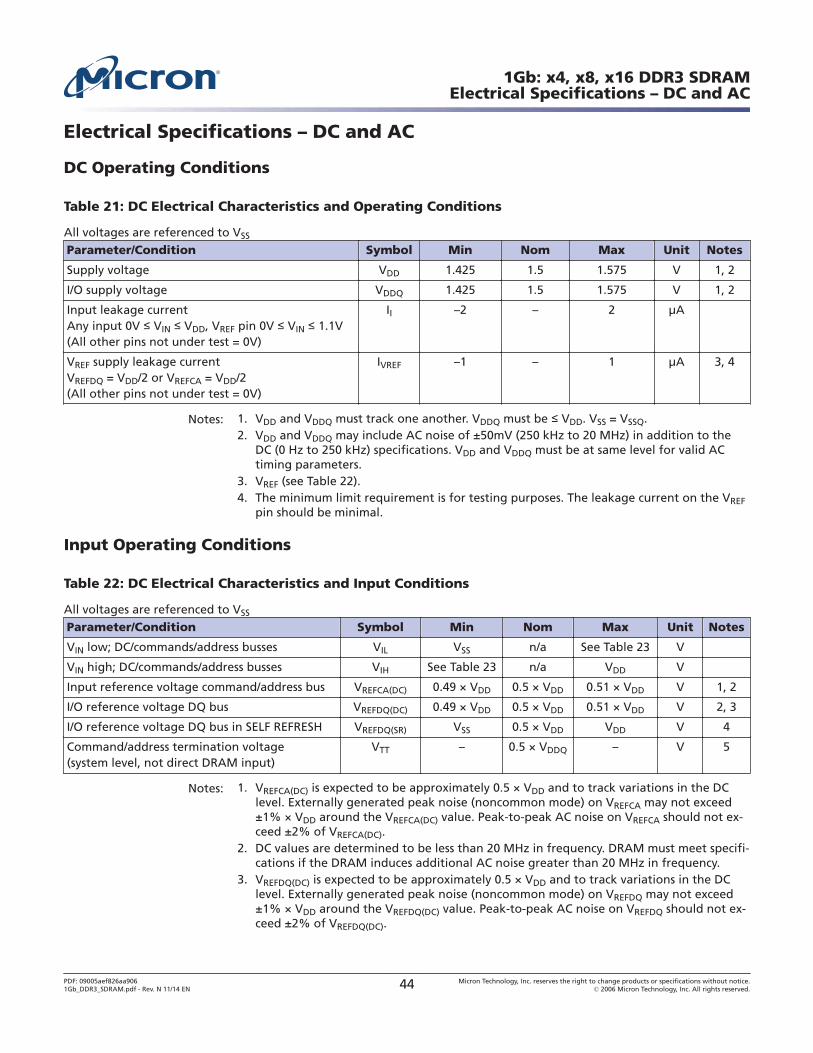
Electrical Specifications – DC and AC
DC Operating Conditions
Table 21: DC Electrical Characteristics and Operating Conditions
All voltages are referenced to VSS
Parameter/Condition Symbol Min Nom Max Unit Notes
Supply voltage VDD 1.425 1.5 1.575 V 1, 2
I/O supply voltage VDDQ 1.425 1.5 1.575 V 1, 2
Input leakage currentAny input 0V ≤ VIN ≤ VDD, VREF pin 0V ≤ VIN ≤ 1.1V(All other pins not under test = 0V)
II –2 – 2 μA
VREF supply leakage currentVREFDQ = VDD/2 or VREFCA = VDD/2(All other pins not under test = 0V)
IVREF –1 – 1 μA 3, 4
Notes: 1. VDD and VDDQ must track one another. VDDQ must be ≤ VDD. VSS = VSSQ.2. VDD and VDDQ may include AC noise of ±50mV (250 kHz to 20 MHz) in addition to the
DC (0 Hz to 250 kHz) specifications. VDD and VDDQ must be at same level for valid ACtiming parameters.
3. VREF (see Table 22).4. The minimum limit requirement is for testing purposes. The leakage current on the VREF
pin should be minimal.
Input Operating Conditions
Table 22: DC Electrical Characteristics and Input Conditions
All voltages are referenced to VSS
Parameter/Condition Symbol Min Nom Max Unit Notes
VIN low; DC/commands/address busses VIL VSS n/a See Table 23 V
VIN high; DC/commands/address busses VIH See Table 23 n/a VDD V
Input reference voltage command/address bus VREFCA(DC) 0.49 × VDD 0.5 × VDD 0.51 × VDD V 1, 2
I/O reference voltage DQ bus VREFDQ(DC) 0.49 × VDD 0.5 × VDD 0.51 × VDD V 2, 3
I/O reference voltage DQ bus in SELF REFRESH VREFDQ(SR) VSS 0.5 × VDD VDD V 4
Command/address termination voltage(system level, not direct DRAM input)
VTT – 0.5 × VDDQ – V 5
Notes: 1. VREFCA(DC) is expected to be approximately 0.5 × VDD and to track variations in the DClevel. Externally generated peak noise (noncommon mode) on VREFCA may not exceed±1% × VDD around the VREFCA(DC) value. Peak-to-peak AC noise on VREFCA should not ex-ceed ±2% of VREFCA(DC).
2. DC values are determined to be less than 20 MHz in frequency. DRAM must meet specifi-cations if the DRAM induces additional AC noise greater than 20 MHz in frequency.
3. VREFDQ(DC) is expected to be approximately 0.5 × VDD and to track variations in the DClevel. Externally generated peak noise (noncommon mode) on VREFDQ may not exceed±1% × VDD around the VREFDQ(DC) value. Peak-to-peak AC noise on VREFDQ should not ex-ceed ±2% of VREFDQ(DC).
1Gb: x4, x8, x16 DDR3 SDRAMElectrical Specifications – DC and AC
PDF: 09005aef826aa9061Gb_DDR3_SDRAM.pdf - Rev. N 11/14 EN 44 Micron Technology, Inc. reserves the right to change products or specifications without notice.
© 2006 Micron Technology, Inc. All rights reserved.
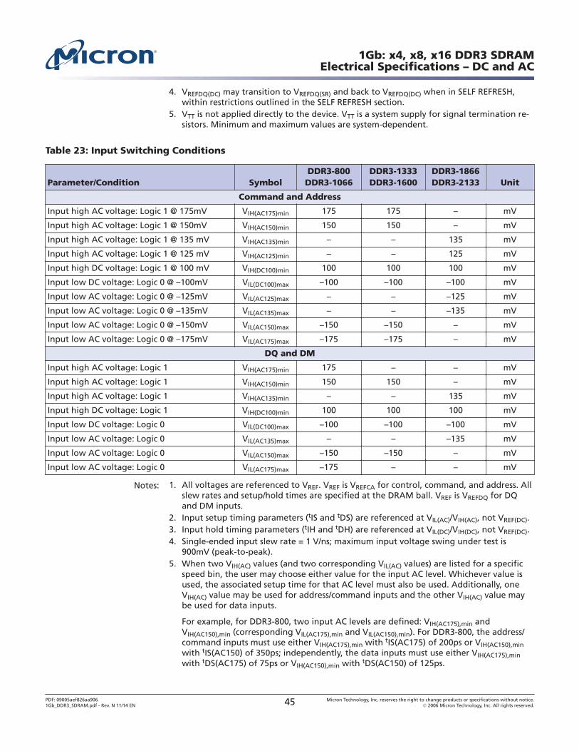
4. VREFDQ(DC) may transition to VREFDQ(SR) and back to VREFDQ(DC) when in SELF REFRESH,within restrictions outlined in the SELF REFRESH section.
5. VTT is not applied directly to the device. VTT is a system supply for signal termination re-sistors. Minimum and maximum values are system-dependent.
Table 23: Input Switching Conditions
Parameter/Condition SymbolDDR3-800DDR3-1066
DDR3-1333DDR3-1600
DDR3-1866DDR3-2133 Unit
Command and Address
Input high AC voltage: Logic 1 @ 175mV VIH(AC175)min 175 175 – mV
Input high AC voltage: Logic 1 @ 150mV VIH(AC150)min 150 150 – mV
Input high AC voltage: Logic 1 @ 135 mV VIH(AC135)min – – 135 mV
Input high AC voltage: Logic 1 @ 125 mV VIH(AC125)min – – 125 mV
Input high DC voltage: Logic 1 @ 100 mV VIH(DC100)min 100 100 100 mV
Input low DC voltage: Logic 0 @ –100mV VIL(DC100)max –100 –100 –100 mV
Input low AC voltage: Logic 0 @ –125mV VIL(AC125)max – – –125 mV
Input low AC voltage: Logic 0 @ –135mV VIL(AC135)max – – –135 mV
Input low AC voltage: Logic 0 @ –150mV VIL(AC150)max –150 –150 – mV
Input low AC voltage: Logic 0 @ –175mV VIL(AC175)max –175 –175 – mV
DQ and DM
Input high AC voltage: Logic 1 VIH(AC175)min 175 – – mV
Input high AC voltage: Logic 1 VIH(AC150)min 150 150 – mV
Input high AC voltage: Logic 1 VIH(AC135)min – – 135 mV
Input high DC voltage: Logic 1 VIH(DC100)min 100 100 100 mV
Input low DC voltage: Logic 0 VIL(DC100)max –100 –100 –100 mV
Input low AC voltage: Logic 0 VIL(AC135)max – – –135 mV
Input low AC voltage: Logic 0 VIL(AC150)max –150 –150 – mV
Input low AC voltage: Logic 0 VIL(AC175)max –175 – – mV
Notes: 1. All voltages are referenced to VREF. VREF is VREFCA for control, command, and address. Allslew rates and setup/hold times are specified at the DRAM ball. VREF is VREFDQ for DQand DM inputs.
2. Input setup timing parameters (tIS and tDS) are referenced at VIL(AC)/VIH(AC), not VREF(DC).3. Input hold timing parameters (tIH and tDH) are referenced at VIL(DC)/VIH(DC), not VREF(DC).4. Single-ended input slew rate = 1 V/ns; maximum input voltage swing under test is
900mV (peak-to-peak).5. When two VIH(AC) values (and two corresponding VIL(AC) values) are listed for a specific
speed bin, the user may choose either value for the input AC level. Whichever value isused, the associated setup time for that AC level must also be used. Additionally, oneVIH(AC) value may be used for address/command inputs and the other VIH(AC) value maybe used for data inputs.
For example, for DDR3-800, two input AC levels are defined: VIH(AC175),min andVIH(AC150),min (corresponding VIL(AC175),min and VIL(AC150),min). For DDR3-800, the address/command inputs must use either VIH(AC175),min with tIS(AC175) of 200ps or VIH(AC150),minwith tIS(AC150) of 350ps; independently, the data inputs must use either VIH(AC175),minwith tDS(AC175) of 75ps or VIH(AC150),min with tDS(AC150) of 125ps.
1Gb: x4, x8, x16 DDR3 SDRAMElectrical Specifications – DC and AC
PDF: 09005aef826aa9061Gb_DDR3_SDRAM.pdf - Rev. N 11/14 EN 45 Micron Technology, Inc. reserves the right to change products or specifications without notice.
© 2006 Micron Technology, Inc. All rights reserved.
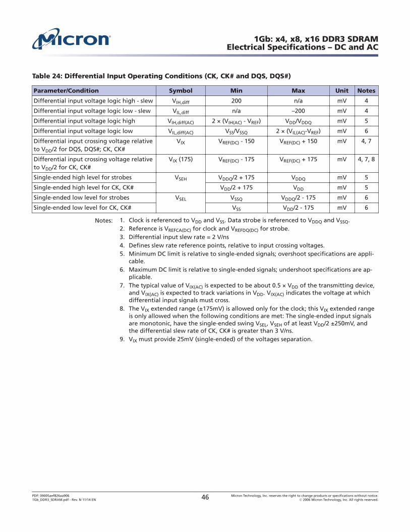
Table 24: Differential Input Operating Conditions (CK, CK# and DQS, DQS#)
Parameter/Condition Symbol Min Max Unit Notes
Differential input voltage logic high - slew VIH,diff 200 n/a mV 4
Differential input voltage logic low - slew VIL,diff n/a –200 mV 4
Differential input voltage logic high VIH,diff(AC) 2 × (VIH(AC) - VREF) VDD/VDDQ mV 5
Differential input voltage logic low VIL,diff(AC) VSS/VSSQ 2 × (VIL(AC)-VREF) mV 6
Differential input crossing voltage relativeto VDD/2 for DQS, DQS#; CK, CK#
VIX VREF(DC) - 150 VREF(DC) + 150 mV 4, 7
Differential input crossing voltage relativeto VDD/2 for CK, CK#
VIX (175) VREF(DC) - 175 VREF(DC) + 175 mV 4, 7, 8
Single-ended high level for strobes VSEH VDDQ/2 + 175 VDDQ mV 5
Single-ended high level for CK, CK# VDD/2 + 175 VDD mV 5
Single-ended low level for strobes VSEL VSSQ VDDQ/2 - 175 mV 6
Single-ended low level for CK, CK# VSS VDD/2 - 175 mV 6
Notes: 1. Clock is referenced to VDD and VSS. Data strobe is referenced to VDDQ and VSSQ.2. Reference is VREFCA(DC) for clock and VREFDQ(DC) for strobe.3. Differential input slew rate = 2 V/ns4. Defines slew rate reference points, relative to input crossing voltages.5. Minimum DC limit is relative to single-ended signals; overshoot specifications are appli-
cable.6. Maximum DC limit is relative to single-ended signals; undershoot specifications are ap-
plicable.7. The typical value of VIX(AC) is expected to be about 0.5 × VDD of the transmitting device,
and VIX(AC) is expected to track variations in VDD. VIX(AC) indicates the voltage at whichdifferential input signals must cross.
8. The VIX extended range (±175mV) is allowed only for the clock; this VIX extended rangeis only allowed when the following conditions are met: The single-ended input signalsare monotonic, have the single-ended swing VSEL, VSEH of at least VDD/2 ±250mV, andthe differential slew rate of CK, CK# is greater than 3 V/ns.
9. VIX must provide 25mV (single-ended) of the voltages separation.
1Gb: x4, x8, x16 DDR3 SDRAMElectrical Specifications – DC and AC
PDF: 09005aef826aa9061Gb_DDR3_SDRAM.pdf - Rev. N 11/14 EN 46 Micron Technology, Inc. reserves the right to change products or specifications without notice.
© 2006 Micron Technology, Inc. All rights reserved.
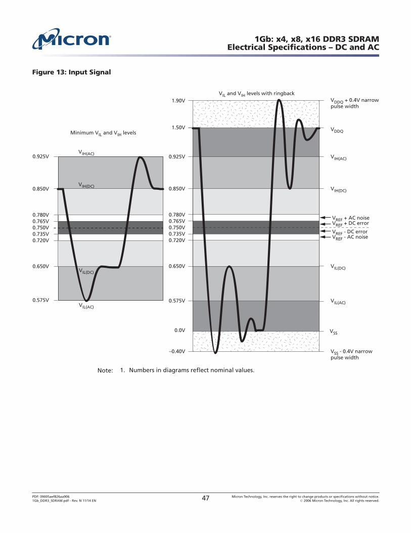
Figure 13: Input Signal
0.575V
0.0V
0.650V
0.720V0.735V0.750V0.765V0.780V
0.850V
0.925V
VIL(AC)
VIL(DC)
VREF - AC noiseVREF - DC error
VREF + DC errorVREF + AC noise
VIH(DC)
VIH(AC)
1.50V
1.90V
–0.40V
VDDQ
VDDQ + 0.4V narrowpulse width
VSS - 0.4V narrowpulse width
VSS
0.575V
0.650V
0.720V0.735V0.750V0.765V0.780V
0.850V
0.925V
Minimum VIL and VIH levels
VIH(DC)
VIH(AC)
VIL(AC)
VIL(DC)
VIL and VIH levels with ringback
Note: 1. Numbers in diagrams reflect nominal values.
1Gb: x4, x8, x16 DDR3 SDRAMElectrical Specifications – DC and AC
PDF: 09005aef826aa9061Gb_DDR3_SDRAM.pdf - Rev. N 11/14 EN 47 Micron Technology, Inc. reserves the right to change products or specifications without notice.
© 2006 Micron Technology, Inc. All rights reserved.
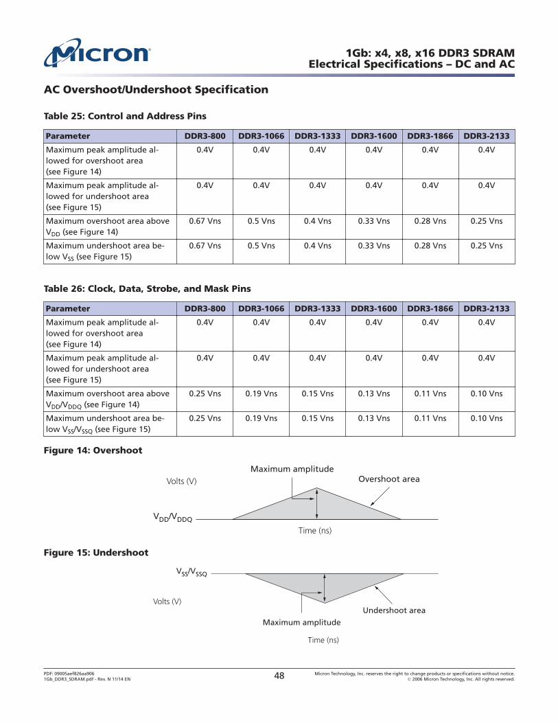
AC Overshoot/Undershoot Specification
Table 25: Control and Address Pins
Parameter DDR3-800 DDR3-1066 DDR3-1333 DDR3-1600 DDR3-1866 DDR3-2133
Maximum peak amplitude al-lowed for overshoot area(see Figure 14)
0.4V 0.4V 0.4V 0.4V 0.4V 0.4V
Maximum peak amplitude al-lowed for undershoot area(see Figure 15)
0.4V 0.4V 0.4V 0.4V 0.4V 0.4V
Maximum overshoot area aboveVDD (see Figure 14)
0.67 Vns 0.5 Vns 0.4 Vns 0.33 Vns 0.28 Vns 0.25 Vns
Maximum undershoot area be-low VSS (see Figure 15)
0.67 Vns 0.5 Vns 0.4 Vns 0.33 Vns 0.28 Vns 0.25 Vns
Table 26: Clock, Data, Strobe, and Mask Pins
Parameter DDR3-800 DDR3-1066 DDR3-1333 DDR3-1600 DDR3-1866 DDR3-2133
Maximum peak amplitude al-lowed for overshoot area(see Figure 14)
0.4V 0.4V 0.4V 0.4V 0.4V 0.4V
Maximum peak amplitude al-lowed for undershoot area(see Figure 15)
0.4V 0.4V 0.4V 0.4V 0.4V 0.4V
Maximum overshoot area aboveVDD/VDDQ (see Figure 14)
0.25 Vns 0.19 Vns 0.15 Vns 0.13 Vns 0.11 Vns 0.10 Vns
Maximum undershoot area be-low VSS/VSSQ (see Figure 15)
0.25 Vns 0.19 Vns 0.15 Vns 0.13 Vns 0.11 Vns 0.10 Vns
Figure 14: Overshoot
Maximum amplitudeOvershoot area
VDD/VDDQ
Time (ns)
Volts (V)
Figure 15: Undershoot
Maximum amplitude
Undershoot area
VSS/VSSQ
Time (ns)
Volts (V)
1Gb: x4, x8, x16 DDR3 SDRAMElectrical Specifications – DC and AC
PDF: 09005aef826aa9061Gb_DDR3_SDRAM.pdf - Rev. N 11/14 EN 48 Micron Technology, Inc. reserves the right to change products or specifications without notice.
© 2006 Micron Technology, Inc. All rights reserved.
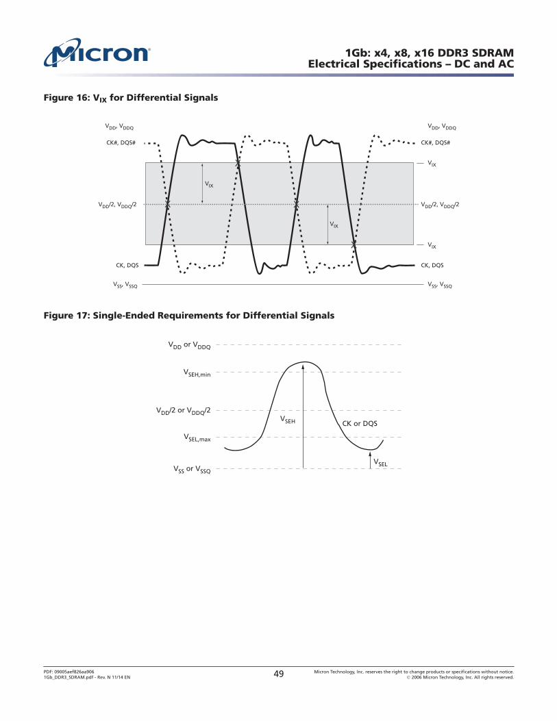
Figure 16: VIX for Differential Signals
CK, DQS
VDD/2, VDDQ/2VDD/2, VDDQ/2
VIX
VIX
CK#, DQS#
VDD, VDDQ
CK, DQS
VDD, VDDQ
VSS, VSSQ
CK#, DQS#
VSS, VSSQ
XX
XX
XX
XX
VIX
VIX
Figure 17: Single-Ended Requirements for Differential Signals
VSS or VSSQ
VDD or VDDQ
VSEL,max
VSEH,min
VSEH
VSEL
CK or DQS
VDD/2 or VDDQ/2
1Gb: x4, x8, x16 DDR3 SDRAMElectrical Specifications – DC and AC
PDF: 09005aef826aa9061Gb_DDR3_SDRAM.pdf - Rev. N 11/14 EN 49 Micron Technology, Inc. reserves the right to change products or specifications without notice.
© 2006 Micron Technology, Inc. All rights reserved.
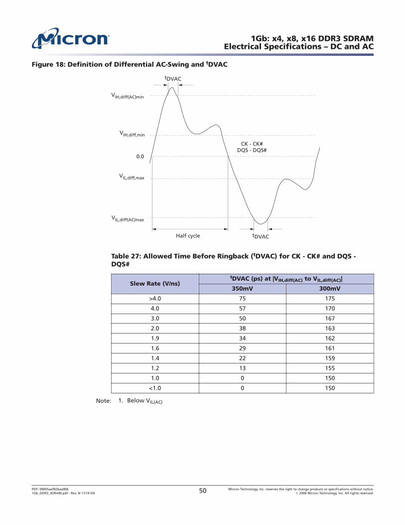
Figure 18: Definition of Differential AC-Swing and tDVAC
VIH,diff(AC)min
0.0
VIL,diff,max
tDVAC
VIH,diff,min
VIL,diff(AC)max
Half cycle tDVAC
CK - CK#DQS - DQS#
Table 27: Allowed Time Before Ringback (tDVAC) for CK - CK# and DQS -DQS#
Slew Rate (V/ns)tDVAC (ps) at |VIH,diff(AC) to VIL,diff(AC)|
350mV 300mV
>4.0 75 175
4.0 57 170
3.0 50 167
2.0 38 163
1.9 34 162
1.6 29 161
1.4 22 159
1.2 13 155
1.0 0 150
<1.0 0 150
Note: 1. Below VIL(AC)
1Gb: x4, x8, x16 DDR3 SDRAMElectrical Specifications – DC and AC
PDF: 09005aef826aa9061Gb_DDR3_SDRAM.pdf - Rev. N 11/14 EN 50 Micron Technology, Inc. reserves the right to change products or specifications without notice.
© 2006 Micron Technology, Inc. All rights reserved.
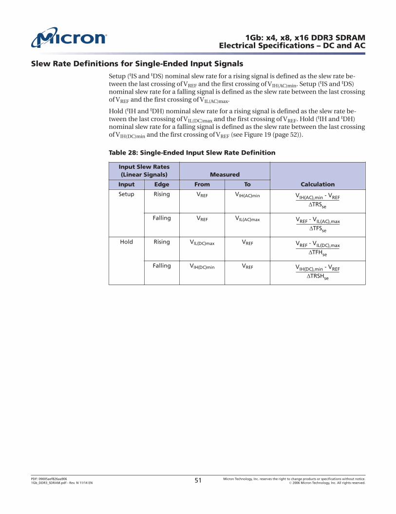
Slew Rate Definitions for Single-Ended Input Signals
Setup (tIS and tDS) nominal slew rate for a rising signal is defined as the slew rate be-tween the last crossing of VREF and the first crossing of VIH(AC)min. Setup (tIS and tDS)nominal slew rate for a falling signal is defined as the slew rate between the last crossingof VREF and the first crossing of VIL(AC)max.
Hold (tIH and tDH) nominal slew rate for a rising signal is defined as the slew rate be-tween the last crossing of VIL(DC)max and the first crossing of VREF. Hold (tIH and tDH)nominal slew rate for a falling signal is defined as the slew rate between the last crossingof VIH(DC)min and the first crossing of VREF (see Figure 19 (page 52)).
Table 28: Single-Ended Input Slew Rate Definition
Input Slew Rates(Linear Signals) Measured
CalculationInput Edge From To
Setup Rising VREF VIH(AC)min VIH(AC),min - VREF
ΔTRSse
Falling VREF VIL(AC)max VREF - VIL(AC),max
ΔTFSse
Hold Rising VIL(DC)max VREF VREF - VIL(DC),max
ΔTFHse
Falling VIH(DC)min VREF VIH(DC),min - VREF
ΔTRSHse
1Gb: x4, x8, x16 DDR3 SDRAMElectrical Specifications – DC and AC
PDF: 09005aef826aa9061Gb_DDR3_SDRAM.pdf - Rev. N 11/14 EN 51 Micron Technology, Inc. reserves the right to change products or specifications without notice.
© 2006 Micron Technology, Inc. All rights reserved.
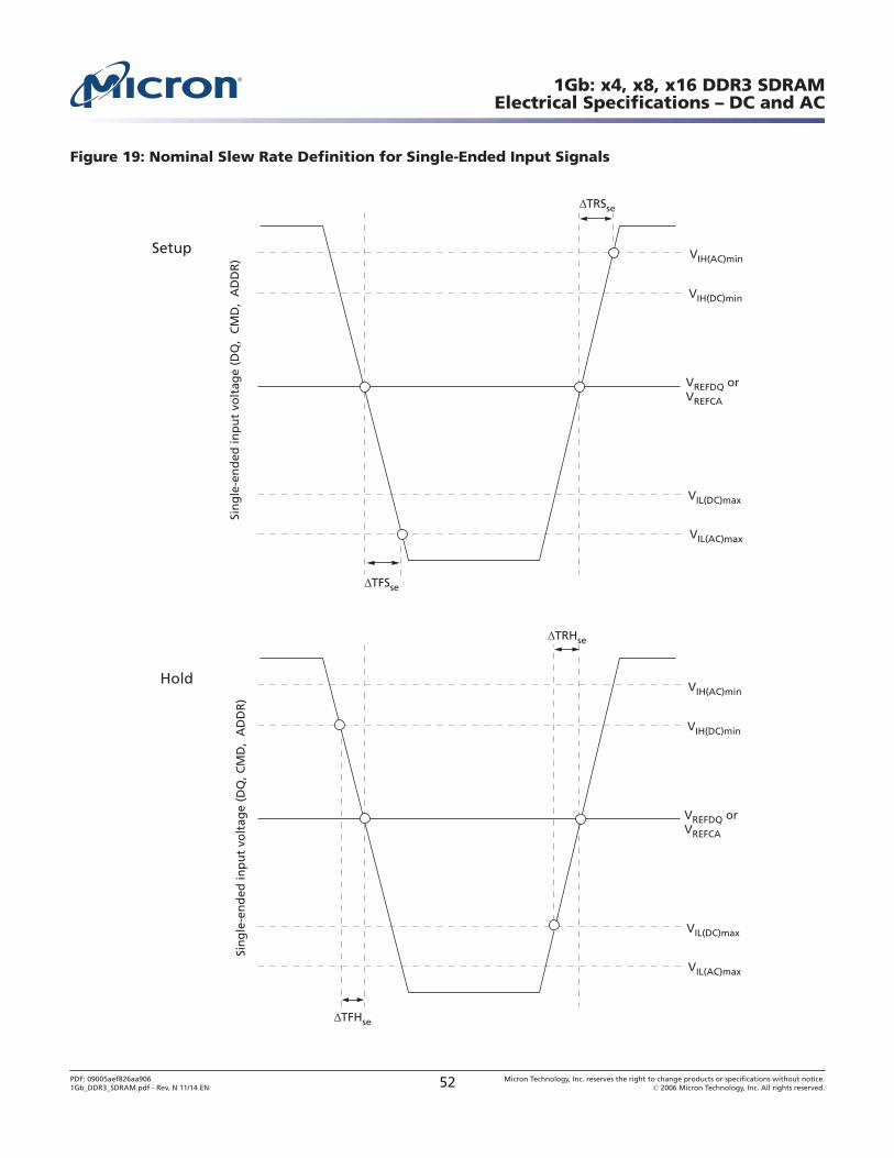
Figure 19: Nominal Slew Rate Definition for Single-Ended Input Signals
ΔTRSse
ΔTFSse
ΔTRHse
ΔTFHse
VREFDQ orVREFCA
VIH(AC)min
VIH(DC)min
VIL(AC)max
VIL(DC)max
VREFDQ or VREFCA
VIH(AC)min
VIH(DC)min
VIL(AC)max
VIL(DC)max
Setup
Hold
Sin
gle
-en
ded
inp
ut
volt
age
(DQ
, C
MD
, A
DD
R)
Sin
gle
-en
ded
inp
ut
volt
age
(DQ
, CM
D,
AD
DR
)
1Gb: x4, x8, x16 DDR3 SDRAMElectrical Specifications – DC and AC
PDF: 09005aef826aa9061Gb_DDR3_SDRAM.pdf - Rev. N 11/14 EN 52 Micron Technology, Inc. reserves the right to change products or specifications without notice.
© 2006 Micron Technology, Inc. All rights reserved.
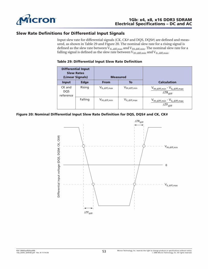
Slew Rate Definitions for Differential Input Signals
Input slew rate for differential signals (CK, CK# and DQS, DQS#) are defined and meas-ured, as shown in Table 29 and Figure 20. The nominal slew rate for a rising signal isdefined as the slew rate between VIL,diff,max and VIH,diff,min. The nominal slew rate for afalling signal is defined as the slew rate between VIH,diff,min and VIL,diff,max.
Table 29: Differential Input Slew Rate Definition
Differential InputSlew Rates
(Linear Signals) Measured
CalculationInput Edge From To
CK andDQS
reference
Rising VIL,diff,max VIH,diff,min VIH,diff,min - VIL,diff,max
ΔTRdiff
Falling VIH,diff,min VIL,diff,max VIH,diff,min - VIL,diff,max
ΔTFdiff
Figure 20: Nominal Differential Input Slew Rate Definition for DQS, DQS# and CK, CK#
ΔTRdiff
ΔTFdiff
VIH,diff,min
VIL,diff,max
0
Dif
fere
nti
al in
pu
t vo
ltag
e (D
QS,
DQ
S#; C
K, C
K#)
1Gb: x4, x8, x16 DDR3 SDRAMElectrical Specifications – DC and AC
PDF: 09005aef826aa9061Gb_DDR3_SDRAM.pdf - Rev. N 11/14 EN 53 Micron Technology, Inc. reserves the right to change products or specifications without notice.
© 2006 Micron Technology, Inc. All rights reserved.
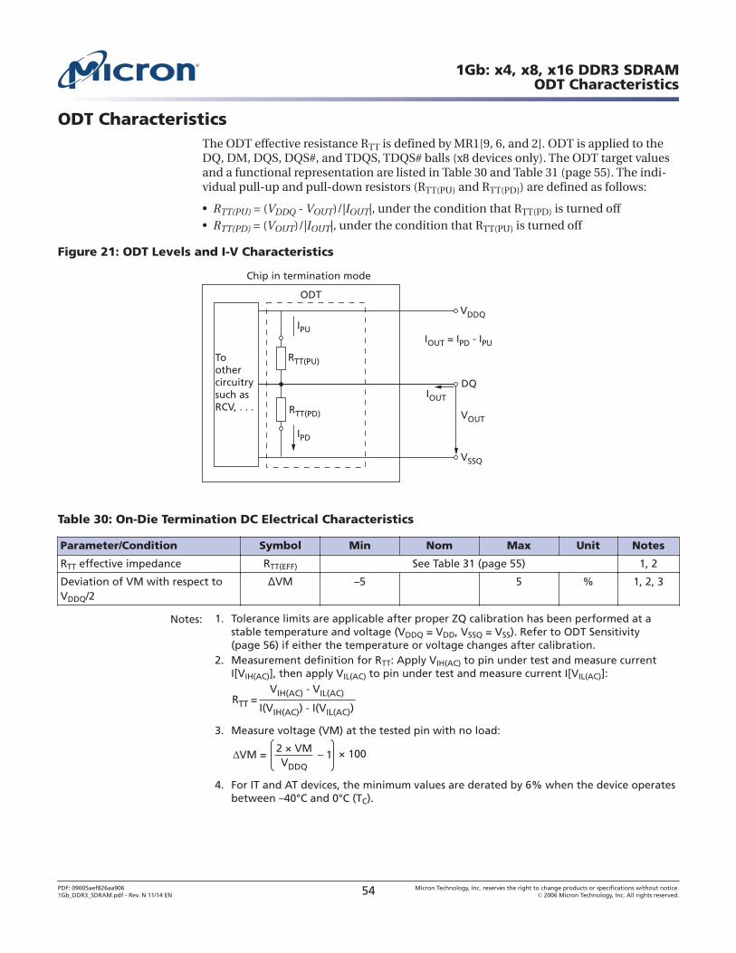
ODT CharacteristicsThe ODT effective resistance RTT is defined by MR1[9, 6, and 2]. ODT is applied to theDQ, DM, DQS, DQS#, and TDQS, TDQS# balls (x8 devices only). The ODT target valuesand a functional representation are listed in Table 30 and Table 31 (page 55). The indi-vidual pull-up and pull-down resistors (RTT(PU) and RTT(PD)) are defined as follows:
• RTT(PU) = (VDDQ - VOUT)/|IOUT|, under the condition that RTT(PD) is turned off• RTT(PD) = (VOUT)/|IOUT|, under the condition that RTT(PU) is turned off
Figure 21: ODT Levels and I-V Characteristics
RTT(PU)
RTT(PD)
ODT
Chip in termination mode
VDDQ
DQ
VSSQ
IOUT = IPD - IPU
IPU
IPD
IOUT
VOUT
Toothercircuitrysuch as RCV, . . .
Table 30: On-Die Termination DC Electrical Characteristics
Parameter/Condition Symbol Min Nom Max Unit Notes
RTT effective impedance RTT(EFF) See Table 31 (page 55) 1, 2
Deviation of VM with respect toVDDQ/2
ΔVM –5 5 % 1, 2, 3
Notes: 1. Tolerance limits are applicable after proper ZQ calibration has been performed at astable temperature and voltage (VDDQ = VDD, VSSQ = VSS). Refer to ODT Sensitivity(page 56) if either the temperature or voltage changes after calibration.
2. Measurement definition for RTT: Apply VIH(AC) to pin under test and measure currentI[VIH(AC)], then apply VIL(AC) to pin under test and measure current I[VIL(AC)]:
RTT = VIH(AC) - VIL(AC)
I(VIH(AC)) - I(VIL(AC))
3. Measure voltage (VM) at the tested pin with no load:
ΔVM = – 12 × VMVDDQ
× 100
4. For IT and AT devices, the minimum values are derated by 6% when the device operatesbetween –40°C and 0°C (TC).
1Gb: x4, x8, x16 DDR3 SDRAMODT Characteristics
PDF: 09005aef826aa9061Gb_DDR3_SDRAM.pdf - Rev. N 11/14 EN 54 Micron Technology, Inc. reserves the right to change products or specifications without notice.
© 2006 Micron Technology, Inc. All rights reserved.
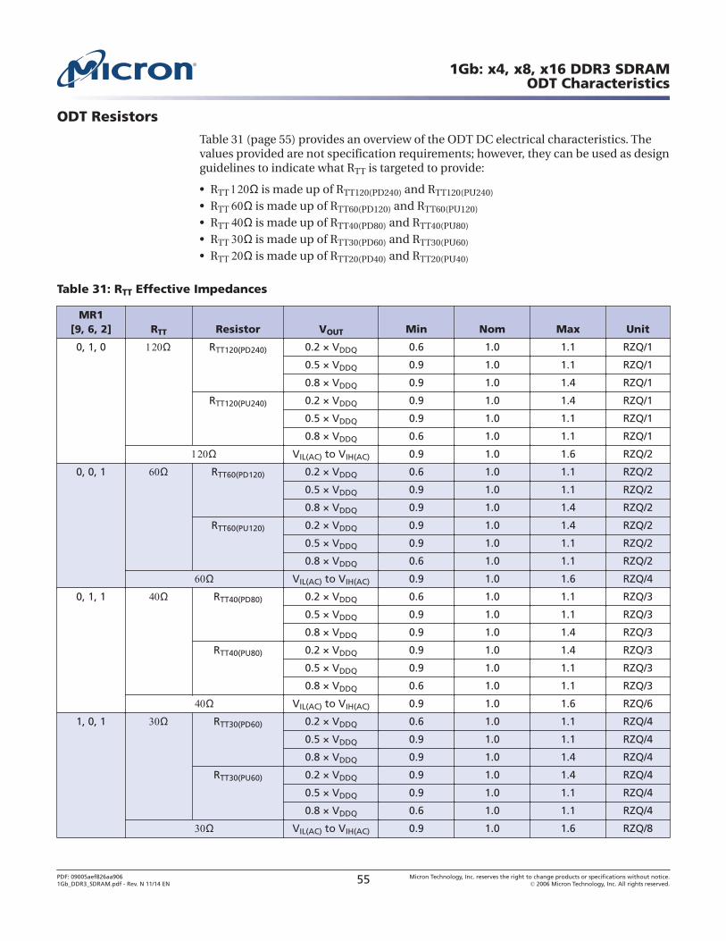
ODT Resistors
Table 31 (page 55) provides an overview of the ODT DC electrical characteristics. Thevalues provided are not specification requirements; however, they can be used as designguidelines to indicate what RTT is targeted to provide:
• RTT Ω is made up of RTT120(PD240) and RTT120(PU240)
• RTT Ω is made up of RTT60(PD120) and RTT60(PU120)
• RTT Ω is made up of RTT40(PD80) and RTT40(PU80)
• RTT Ω is made up of RTT30(PD60) and RTT30(PU60)
• RTT Ω is made up of RTT20(PD40) and RTT20(PU40)
Table 31: RTT Effective Impedances
MR1[9, 6, 2] RTT Resistor VOUT Min Nom Max Unit
0, 1, 0 Ω RTT120(PD240) 0.2 × VDDQ 0.6 1.0 1.1 RZQ/1
0.5 × VDDQ 0.9 1.0 1.1 RZQ/1
0.8 × VDDQ 0.9 1.0 1.4 RZQ/1
RTT120(PU240) 0.2 × VDDQ 0.9 1.0 1.4 RZQ/1
0.5 × VDDQ 0.9 1.0 1.1 RZQ/1
0.8 × VDDQ 0.6 1.0 1.1 RZQ/1
Ω VIL(AC) to VIH(AC) 0.9 1.0 1.6 RZQ/2
0, 0, 1 Ω RTT60(PD120) 0.2 × VDDQ 0.6 1.0 1.1 RZQ/2
0.5 × VDDQ 0.9 1.0 1.1 RZQ/2
0.8 × VDDQ 0.9 1.0 1.4 RZQ/2
RTT60(PU120) 0.2 × VDDQ 0.9 1.0 1.4 RZQ/2
0.5 × VDDQ 0.9 1.0 1.1 RZQ/2
0.8 × VDDQ 0.6 1.0 1.1 RZQ/2
Ω VIL(AC) to VIH(AC) 0.9 1.0 1.6 RZQ/4
0, 1, 1 Ω RTT40(PD80) 0.2 × VDDQ 0.6 1.0 1.1 RZQ/3
0.5 × VDDQ 0.9 1.0 1.1 RZQ/3
0.8 × VDDQ 0.9 1.0 1.4 RZQ/3
RTT40(PU80) 0.2 × VDDQ 0.9 1.0 1.4 RZQ/3
0.5 × VDDQ 0.9 1.0 1.1 RZQ/3
0.8 × VDDQ 0.6 1.0 1.1 RZQ/3
Ω VIL(AC) to VIH(AC) 0.9 1.0 1.6 RZQ/6
1, 0, 1 Ω RTT30(PD60) 0.2 × VDDQ 0.6 1.0 1.1 RZQ/4
0.5 × VDDQ 0.9 1.0 1.1 RZQ/4
0.8 × VDDQ 0.9 1.0 1.4 RZQ/4
RTT30(PU60) 0.2 × VDDQ 0.9 1.0 1.4 RZQ/4
0.5 × VDDQ 0.9 1.0 1.1 RZQ/4
0.8 × VDDQ 0.6 1.0 1.1 RZQ/4
Ω VIL(AC) to VIH(AC) 0.9 1.0 1.6 RZQ/8
1Gb: x4, x8, x16 DDR3 SDRAMODT Characteristics
PDF: 09005aef826aa9061Gb_DDR3_SDRAM.pdf - Rev. N 11/14 EN 55 Micron Technology, Inc. reserves the right to change products or specifications without notice.
© 2006 Micron Technology, Inc. All rights reserved.
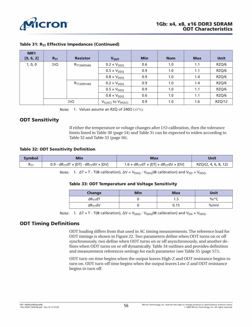
Table 31: RTT Effective Impedances (Continued)
MR1[9, 6, 2] RTT Resistor VOUT Min Nom Max Unit
1, 0, 0 Ω RTT20(PD40) 0.2 × VDDQ 0.6 1.0 1.1 RZQ/6
0.5 × VDDQ 0.9 1.0 1.1 RZQ/6
0.8 × VDDQ 0.9 1.0 1.4 RZQ/6
RTT20(PU40) 0.2 × VDDQ 0.9 1.0 1.4 RZQ/6
0.5 × VDDQ 0.9 1.0 1.1 RZQ/6
0.8 × VDDQ 0.6 1.0 1.1 RZQ/6
Ω VIL(AC) to VIH(AC) 0.9 1.0 1.6 RZQ/12
Note: 1. Values assume an RZQ of 240Ω
ODT Sensitivity
If either the temperature or voltage changes after I/O calibration, then the tolerancelimits listed in Table 30 (page 54) and Table 31 can be expected to widen according toTable 32 and Table 33 (page 56).
Table 32: ODT Sensitivity Definition
Symbol Min Max Unit
RTT 0.9 - dRTTdT × |DT| - dRTTdV × |DV| 1.6 + dRTTdT × |DT| + dRTTdV × |DV| RZQ/(2, 4, 6, 8, 12)
Note: 1. ΔT = T - T(@ calibration), ΔV = VDDQ - VDDQ(@ calibration) and VDD = VDDQ.
Table 33: ODT Temperature and Voltage Sensitivity
Change Min Max Unit
dRTTdT 0 1.5 %/°C
dRTTdV 0 0.15 %/mV
Note: 1. ΔT = T - T(@ calibration), ΔV = VDDQ - VDDQ(@ calibration) and VDD = VDDQ.
ODT Timing Definitions
ODT loading differs from that used in AC timing measurements. The reference load forODT timings is shown in Figure 22. Two parameters define when ODT turns on or offsynchronously, two define when ODT turns on or off asynchronously, and another de-fines when ODT turns on or off dynamically. Table 34 outlines and provides definitionand measurement references settings for each parameter (see Table 35 (page 57)).
ODT turn-on time begins when the output leaves High-Z and ODT resistance begins toturn on. ODT turn-off time begins when the output leaves Low-Z and ODT resistancebegins to turn off.
1Gb: x4, x8, x16 DDR3 SDRAMODT Characteristics
PDF: 09005aef826aa9061Gb_DDR3_SDRAM.pdf - Rev. N 11/14 EN 56 Micron Technology, Inc. reserves the right to change products or specifications without notice.
© 2006 Micron Technology, Inc. All rights reserved.
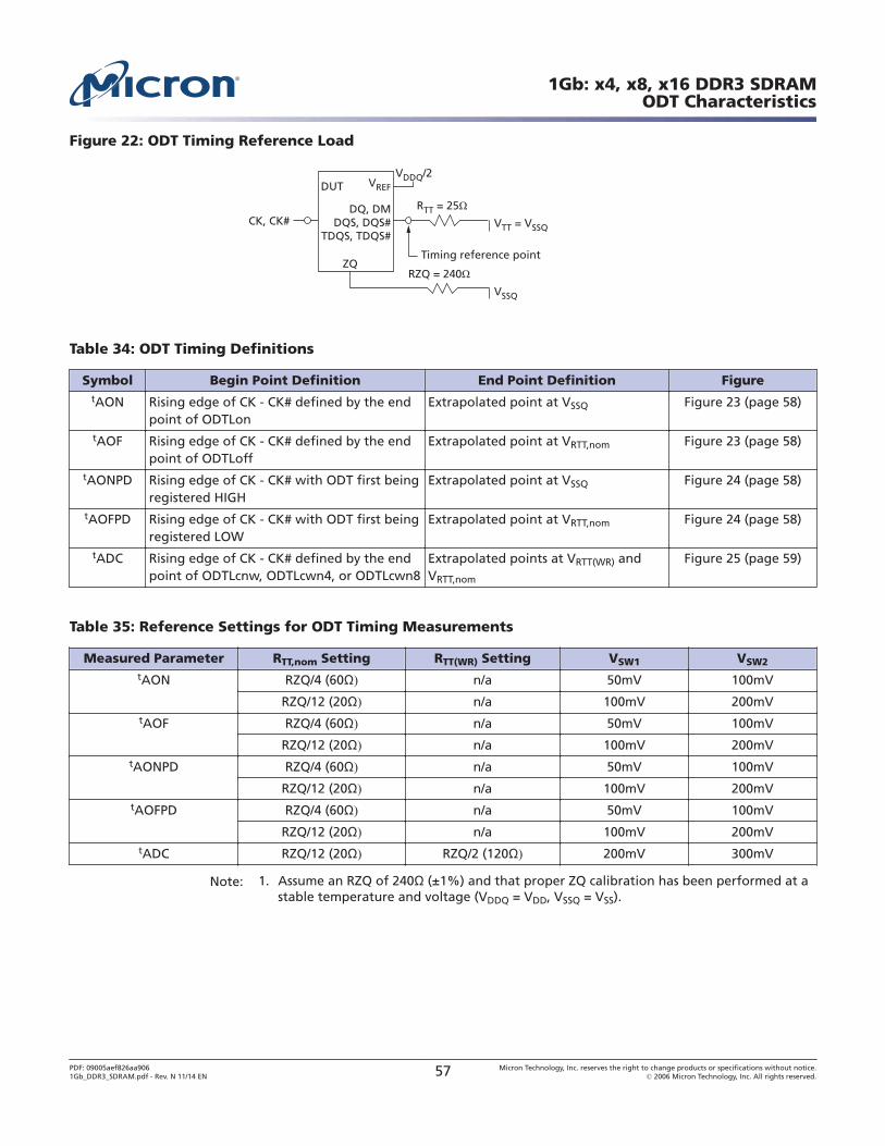
Figure 22: ODT Timing Reference Load
Timing reference point
DQ, DMDQS, DQS#
TDQS, TDQS#
DUT VREF
VTT = VSSQ
VDDQ/2
ZQRZQ = 240Ω
VSSQ
RTT = 25ΩCK, CK#
Table 34: ODT Timing Definitions
Symbol Begin Point Definition End Point Definition FiguretAON Rising edge of CK - CK# defined by the end
point of ODTLonExtrapolated point at VSSQ Figure 23 (page 58)
tAOF Rising edge of CK - CK# defined by the endpoint of ODTLoff
Extrapolated point at VRTT,nom Figure 23 (page 58)
tAONPD Rising edge of CK - CK# with ODT first beingregistered HIGH
Extrapolated point at VSSQ Figure 24 (page 58)
tAOFPD Rising edge of CK - CK# with ODT first beingregistered LOW
Extrapolated point at VRTT,nom Figure 24 (page 58)
tADC Rising edge of CK - CK# defined by the endpoint of ODTLcnw, ODTLcwn4, or ODTLcwn8
Extrapolated points at VRTT(WR) andVRTT,nom
Figure 25 (page 59)
Table 35: Reference Settings for ODT Timing Measurements
Measured Parameter RTT,nom Setting RTT(WR) Setting VSW1 VSW2
tAON RZQ/4 (60Ω n/a 50mV 100mV
RZQ/12 (20Ω n/a 100mV 200mVtAOF RZQ/4 (60Ω n/a 50mV 100mV
RZQ/12 (20Ω n/a 100mV 200mVtAONPD RZQ/4 (60Ω n/a 50mV 100mV
RZQ/12 (20Ω n/a 100mV 200mVtAOFPD RZQ/4 (60Ω n/a 50mV 100mV
RZQ/12 (20Ω n/a 100mV 200mVtADC RZQ/12 (20Ω RZQ/2 (120Ω 200mV 300mV
Note: 1. Assume an RZQ of 240Ω (±1%) and that proper ZQ calibration has been performed at astable temperature and voltage (VDDQ = VDD, VSSQ = VSS).
1Gb: x4, x8, x16 DDR3 SDRAMODT Characteristics
PDF: 09005aef826aa9061Gb_DDR3_SDRAM.pdf - Rev. N 11/14 EN 57 Micron Technology, Inc. reserves the right to change products or specifications without notice.
© 2006 Micron Technology, Inc. All rights reserved.
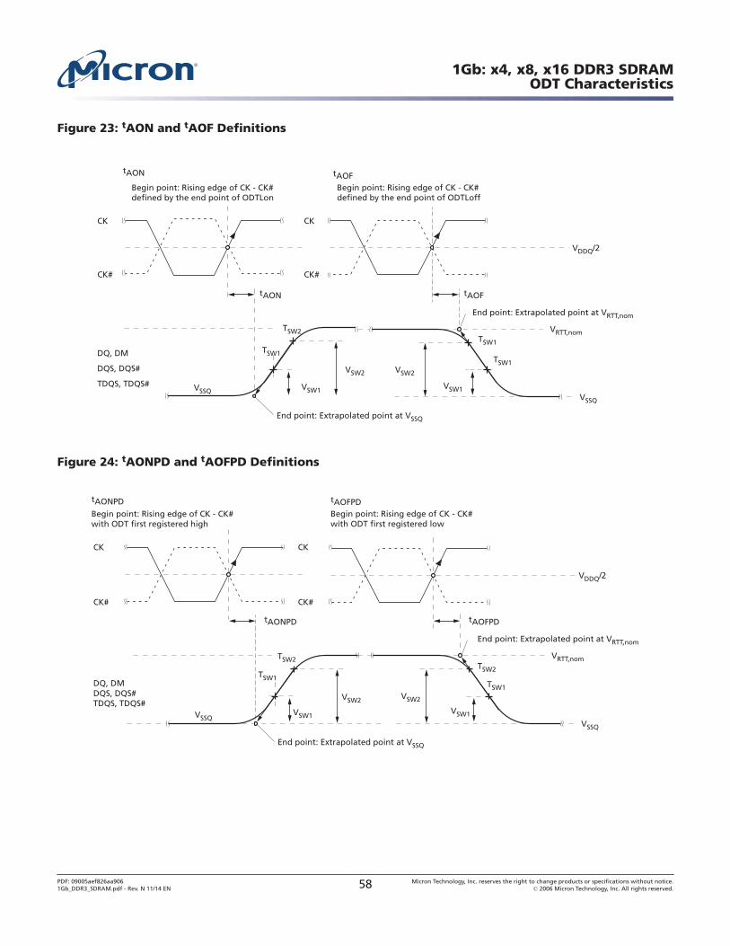
Figure 23: tAON and tAOF Definitions
CK
CK#
tAON
VSSQ
DQ, DM
DQS, DQS#
TDQS, TDQS#
Begin point: Rising edge of CK - CK# defined by the end point of ODTLon
VSW1
End point: Extrapolated point at VSSQ
TSW1
TSW2
CK
CK#
VDDQ/2
tAOF
Begin point: Rising edge of CK - CK# defined by the end point of ODTLoff
End point: Extrapolated point at VRTT,nom
VRTT,nom
VSSQ
tAON tAOF
VSW2 VSW2
VSW1
TSW1
TSW1
Figure 24: tAONPD and tAOFPD Definitions
CK
CK#
tAONPD
VSSQ
DQ, DM DQS, DQS# TDQS, TDQS#
Begin point: Rising edge of CK - CK# with ODT first registered high
VSW1
End point: Extrapolated point at VSSQ
TSW2
CK
CK#
VDDQ/2
tAOFPD
Begin point: Rising edge of CK - CK# with ODT first registered low
End point: Extrapolated point at VRTT,nom
VRTT,nom
VSSQ
tAONPD tAOFPD
TSW1
TSW2
TSW1
VSW2 VSW2
VSW1
1Gb: x4, x8, x16 DDR3 SDRAMODT Characteristics
PDF: 09005aef826aa9061Gb_DDR3_SDRAM.pdf - Rev. N 11/14 EN 58 Micron Technology, Inc. reserves the right to change products or specifications without notice.
© 2006 Micron Technology, Inc. All rights reserved.
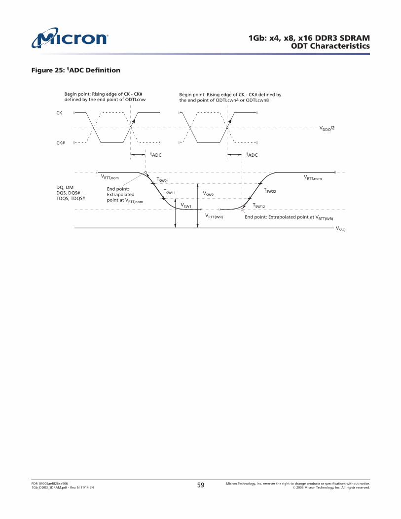
Figure 25: tADC Definition
CK
CK#
tADC
DQ, DM DQS, DQS# TDQS, TDQS#
End point: Extrapolated point at VRTT,nom
TSW21
tADC
End point: Extrapolated point at VRTT(WR)
VDDQ/2
VSSQ
VRTT,nom
VRTT(WR)
VRTT,nom
Begin point: Rising edge of CK - CK# defined by the end point of ODTLcnw
Begin point: Rising edge of CK - CK# defined by the end point of ODTLcwn4 or ODTLcwn8
TSW11
VSW1
VSW2
TSW12
TSW22
1Gb: x4, x8, x16 DDR3 SDRAMODT Characteristics
PDF: 09005aef826aa9061Gb_DDR3_SDRAM.pdf - Rev. N 11/14 EN 59 Micron Technology, Inc. reserves the right to change products or specifications without notice.
© 2006 Micron Technology, Inc. All rights reserved.
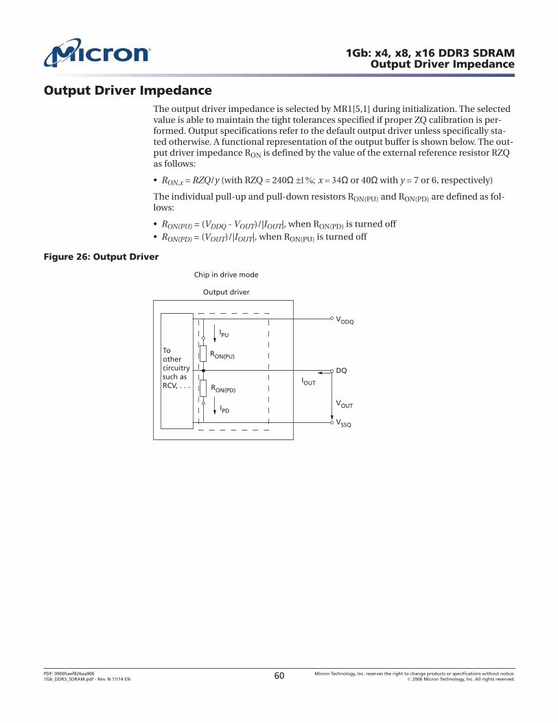
Output Driver ImpedanceThe output driver impedance is selected by MR1[5,1] during initialization. The selectedvalue is able to maintain the tight tolerances specified if proper ZQ calibration is per-formed. Output specifications refer to the default output driver unless specifically sta-ted otherwise. A functional representation of the output buffer is shown below. The out-put driver impedance RON is defined by the value of the external reference resistor RZQas follows:
• RON,x = RZQ/y (with RZQ = 240Ω x Ω or 40Ω with y = 7 or 6, respectively)
The individual pull-up and pull-down resistors RON(PU) and RON(PD) are defined as fol-lows:
• RON(PU) = (VDDQ - VOUT)/|IOUT|, when RON(PD) is turned off• RON(PD) = (VOUT)/|IOUT|, when RON(PU) is turned off
Figure 26: Output Driver
RON(PU)
RON(PD)
Output driver
Toothercircuitrysuch asRCV, . . .
Chip in drive mode
VDDQ
VSSQ
IPU
IPD
IOUT
VOUT
DQ
1Gb: x4, x8, x16 DDR3 SDRAMOutput Driver Impedance
PDF: 09005aef826aa9061Gb_DDR3_SDRAM.pdf - Rev. N 11/14 EN 60 Micron Technology, Inc. reserves the right to change products or specifications without notice.
© 2006 Micron Technology, Inc. All rights reserved.
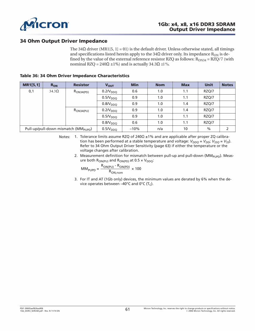
34 Ohm Output Driver Impedance
The 34Ω driver (MR1[5, 1] = 01) is the default driver. Unless otherwise stated, all timingsand specifications listed herein apply to the 34Ω driver only. Its impedance RON is de-fined by the value of the external reference resistor RZQ as follows: RON34 = RZQ/7 (withnominal RZQ = 240Ω ±1%) and is actually 34.3Ω
Table 36: 34 Ohm Driver Impedance Characteristics
MR1[5,1] RON Resistor VOUT Min Nom Max Unit Notes
0,1 Ω RON34(PD) 0.2/VDDQ 0.6 1.0 1.1 RZQ/7
0.5/VDDQ 0.9 1.0 1.1 RZQ/7
0.8/VDDQ 0.9 1.0 1.4 RZQ/7
RON34(PU) 0.2/VDDQ 0.9 1.0 1.4 RZQ/7
0.5/VDDQ 0.9 1.0 1.1 RZQ/7
0.8/VDDQ 0.6 1.0 1.1 RZQ/7
Pull-up/pull-down mismatch (MMPUPD) 0.5/VDDQ –10% n/a 10 % 2
Notes: 1. Tolerance limits assume RZQ of 240Ω ±1% and are applicable after proper ZQ calibra-tion has been performed at a stable temperature and voltage: VDDQ = VDD; VSSQ = VSS).Refer to 34 Ohm Output Driver Sensitivity (page 63) if either the temperature or thevoltage changes after calibration.
2. Measurement definition for mismatch between pull-up and pull-down (MMPUPD). Meas-ure both RON(PU) and RON(PD) at 0.5 × VDDQ:
MMPUPD = × 100RON(PU) - RON(PD)
RON,nom
3. For IT and AT (1Gb only) devices, the minimum values are derated by 6% when the de-vice operates between –40°C and 0°C (TC).
1Gb: x4, x8, x16 DDR3 SDRAMOutput Driver Impedance
PDF: 09005aef826aa9061Gb_DDR3_SDRAM.pdf - Rev. N 11/14 EN 61 Micron Technology, Inc. reserves the right to change products or specifications without notice.
© 2006 Micron Technology, Inc. All rights reserved.
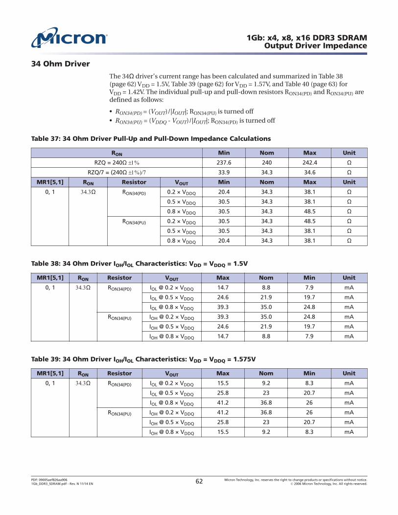
34 Ohm Driver
The 34Ω driver’s current range has been calculated and summarized in Table 38(page 62) VDD = 1.5V, Table 39 (page 62) for VDD = 1.57V, and Table 40 (page 63) forVDD = 1.42V. The individual pull-up and pull-down resistors RON34(PD) and RON34(PU) aredefined as follows:
• RON34(PD) = (VOUT)/|IOUT|; RON34(PU) is turned off• RON34(PU) = (VDDQ - VOUT)/|IOUT|; RON34(PD) is turned off
Table 37: 34 Ohm Driver Pull-Up and Pull-Down Impedance Calculations
RON Min Nom Max Unit
RZQ = 240Ω 237.6 240 242.4 ΩRZQ/7 = (240Ω 33.9 34.3 34.6 Ω
MR1[5,1] RON Resistor VOUT Min Nom Max Unit
0, 1 Ω RON34(PD) 0.2 × VDDQ 20.4 34.3 38.1 Ω0.5 × VDDQ 30.5 34.3 38.1 Ω0.8 × VDDQ 30.5 34.3 48.5 Ω
RON34(PU) 0.2 × VDDQ 30.5 34.3 48.5 Ω0.5 × VDDQ 30.5 34.3 38.1 Ω0.8 × VDDQ 20.4 34.3 38.1 Ω
Table 38: 34 Ohm Driver IOH/IOL Characteristics: VDD = VDDQ = 1.5V
MR1[5,1] RON Resistor VOUT Max Nom Min Unit
0, 1 Ω RON34(PD) IOL @ 0.2 × VDDQ 14.7 8.8 7.9 mA
IOL @ 0.5 × VDDQ 24.6 21.9 19.7 mA
IOL @ 0.8 × VDDQ 39.3 35.0 24.8 mA
RON34(PU) IOH @ 0.2 × VDDQ 39.3 35.0 24.8 mA
IOH @ 0.5 × VDDQ 24.6 21.9 19.7 mA
IOH @ 0.8 × VDDQ 14.7 8.8 7.9 mA
Table 39: 34 Ohm Driver IOH/IOL Characteristics: VDD = VDDQ = 1.575V
MR1[5,1] RON Resistor VOUT Max Nom Min Unit
0, 1 Ω RON34(PD) IOL @ 0.2 × VDDQ 15.5 9.2 8.3 mA
IOL @ 0.5 × VDDQ 25.8 23 20.7 mA
IOL @ 0.8 × VDDQ 41.2 36.8 26 mA
RON34(PU) IOH @ 0.2 × VDDQ 41.2 36.8 26 mA
IOH @ 0.5 × VDDQ 25.8 23 20.7 mA
IOH @ 0.8 × VDDQ 15.5 9.2 8.3 mA
1Gb: x4, x8, x16 DDR3 SDRAMOutput Driver Impedance
PDF: 09005aef826aa9061Gb_DDR3_SDRAM.pdf - Rev. N 11/14 EN 62 Micron Technology, Inc. reserves the right to change products or specifications without notice.
© 2006 Micron Technology, Inc. All rights reserved.
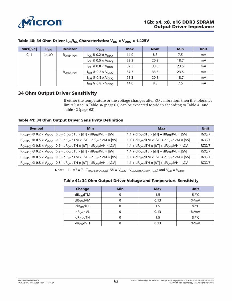
Table 40: 34 Ohm Driver IOH/IOL Characteristics: VDD = VDDQ = 1.425V
MR1[5,1] RON Resistor VOUT Max Nom Min Unit
0, 1 Ω RON34(PD) IOL @ 0.2 × VDDQ 14.0 8.3 7.5 mA
IOL @ 0.5 × VDDQ 23.3 20.8 18.7 mA
IOL @ 0.8 × VDDQ 37.3 33.3 23.5 mA
RON34(PU) IOH @ 0.2 × VDDQ 37.3 33.3 23.5 mA
IOH @ 0.5 × VDDQ 23.3 20.8 18.7 mA
IOH @ 0.8 × VDDQ 14.0 8.3 7.5 mA
34 Ohm Output Driver Sensitivity
If either the temperature or the voltage changes after ZQ calibration, then the tolerancelimits listed in Table 36 (page 61) can be expected to widen according to Table 41 andTable 42 (page 63).
Table 41: 34 Ohm Output Driver Sensitivity Definition
Symbol Min Max Unit
RON(PD) @ 0.2 × VDDQ 0.6 - dRONdTL × |ΔT| - dRONdVL × |ΔV| 1.1 + dRONdTL × |ΔT| + dRONdVL × |ΔV| RZQ/7
RON(PD) @ 0.5 × VDDQ 0.9 - dRONdTM × |ΔT| - dRONdVM × |ΔV| 1.1 + dRONdTM × |ΔT| + dRONdVM × |ΔV| RZQ/7
RON(PD) @ 0.8 × VDDQ 0.9 - dRONdTH × |ΔT| - dRONdVH × |ΔV| 1.4 + dRONdTH × |ΔT| + dRONdVH × |ΔV| RZQ/7
RON(PU) @ 0.2 × VDDQ 0.9 - dRONdTL × |ΔT| - dRONdVL × |ΔV| 1.4 + dRONdTL × |ΔT| + dRONdVL × |ΔV| RZQ/7
RON(PU) @ 0.5 × VDDQ 0.9 - dRONdTM × |ΔT| - dRONdVM × |ΔV| 1.1 + dRONdTM × |ΔT| + dRONdVM × |ΔV| RZQ/7
RON(PU) @ 0.8 × VDDQ 0.6 - dRONdTH × |ΔT| - dRONdVH × |ΔV| 1.1 + dRONdTH × |ΔT| + dRONdVH × |ΔV| RZQ/7
Note: 1. ΔT = T - T(@CALIBRATION)ΔV = VDDQ - VDDQ(@CALIBRATION); and VDD = VDDQ.
Table 42: 34 Ohm Output Driver Voltage and Temperature Sensitivity
Change Min Max Unit
dRONdTM 0 1.5 %/°C
dRONdVM 0 0.13 %/mV
dRONdTL 0 1.5 %/°C
dRONdVL 0 0.13 %/mV
dRONdTH 0 1.5 %/°C
dRONdVH 0 0.13 %/mV
1Gb: x4, x8, x16 DDR3 SDRAMOutput Driver Impedance
PDF: 09005aef826aa9061Gb_DDR3_SDRAM.pdf - Rev. N 11/14 EN 63 Micron Technology, Inc. reserves the right to change products or specifications without notice.
© 2006 Micron Technology, Inc. All rights reserved.
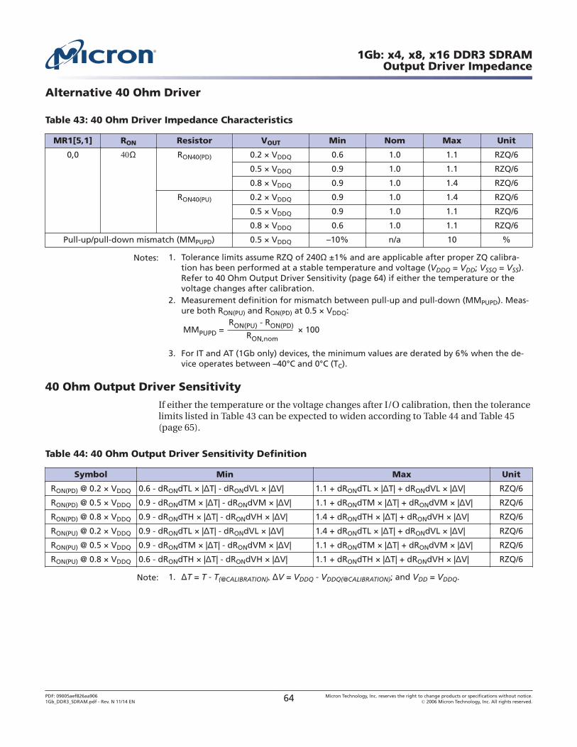
Alternative 40 Ohm Driver
Table 43: 40 Ohm Driver Impedance Characteristics
MR1[5,1] RON Resistor VOUT Min Nom Max Unit
0,0 Ω RON40(PD) 0.2 × VDDQ 0.6 1.0 1.1 RZQ/6
0.5 × VDDQ 0.9 1.0 1.1 RZQ/6
0.8 × VDDQ 0.9 1.0 1.4 RZQ/6
RON40(PU) 0.2 × VDDQ 0.9 1.0 1.4 RZQ/6
0.5 × VDDQ 0.9 1.0 1.1 RZQ/6
0.8 × VDDQ 0.6 1.0 1.1 RZQ/6
Pull-up/pull-down mismatch (MMPUPD) 0.5 × VDDQ –10% n/a 10 %
Notes: 1. Tolerance limits assume RZQ of 240Ω ±1% and are applicable after proper ZQ calibra-tion has been performed at a stable temperature and voltage (VDDQ = VDD; VSSQ = VSS).Refer to 40 Ohm Output Driver Sensitivity (page 64) if either the temperature or thevoltage changes after calibration.
2. Measurement definition for mismatch between pull-up and pull-down (MMPUPD). Meas-ure both RON(PU) and RON(PD) at 0.5 × VDDQ:
MMPUPD = × 100RON(PU) - RON(PD)
RON,nom
3. For IT and AT (1Gb only) devices, the minimum values are derated by 6% when the de-vice operates between –40°C and 0°C (TC).
40 Ohm Output Driver Sensitivity
If either the temperature or the voltage changes after I/O calibration, then the tolerancelimits listed in Table 43 can be expected to widen according to Table 44 and Table 45(page 65).
Table 44: 40 Ohm Output Driver Sensitivity Definition
Symbol Min Max Unit
RON(PD) @ 0.2 × VDDQ 0.6 - dRONdTL × |ΔT| - dRONdVL × |ΔV| 1.1 + dRONdTL × |ΔT| + dRONdVL × |ΔV| RZQ/6
RON(PD) @ 0.5 × VDDQ 0.9 - dRONdTM × |ΔT| - dRONdVM × |ΔV| 1.1 + dRONdTM × |ΔT| + dRONdVM × |ΔV| RZQ/6
RON(PD) @ 0.8 × VDDQ 0.9 - dRONdTH × |ΔT| - dRONdVH × |ΔV| 1.4 + dRONdTH × |ΔT| + dRONdVH × |ΔV| RZQ/6
RON(PU) @ 0.2 × VDDQ 0.9 - dRONdTL × |ΔT| - dRONdVL × |ΔV| 1.4 + dRONdTL × |ΔT| + dRONdVL × |ΔV| RZQ/6
RON(PU) @ 0.5 × VDDQ 0.9 - dRONdTM × |ΔT| - dRONdVM × |ΔV| 1.1 + dRONdTM × |ΔT| + dRONdVM × |ΔV| RZQ/6
RON(PU) @ 0.8 × VDDQ 0.6 - dRONdTH × |ΔT| - dRONdVH × |ΔV| 1.1 + dRONdTH × |ΔT| + dRONdVH × |ΔV| RZQ/6
Note: 1. ΔT = T - T(@CALIBRATION)ΔV = VDDQ - VDDQ(@CALIBRATION); and VDD = VDDQ.
1Gb: x4, x8, x16 DDR3 SDRAMOutput Driver Impedance
PDF: 09005aef826aa9061Gb_DDR3_SDRAM.pdf - Rev. N 11/14 EN 64 Micron Technology, Inc. reserves the right to change products or specifications without notice.
© 2006 Micron Technology, Inc. All rights reserved.
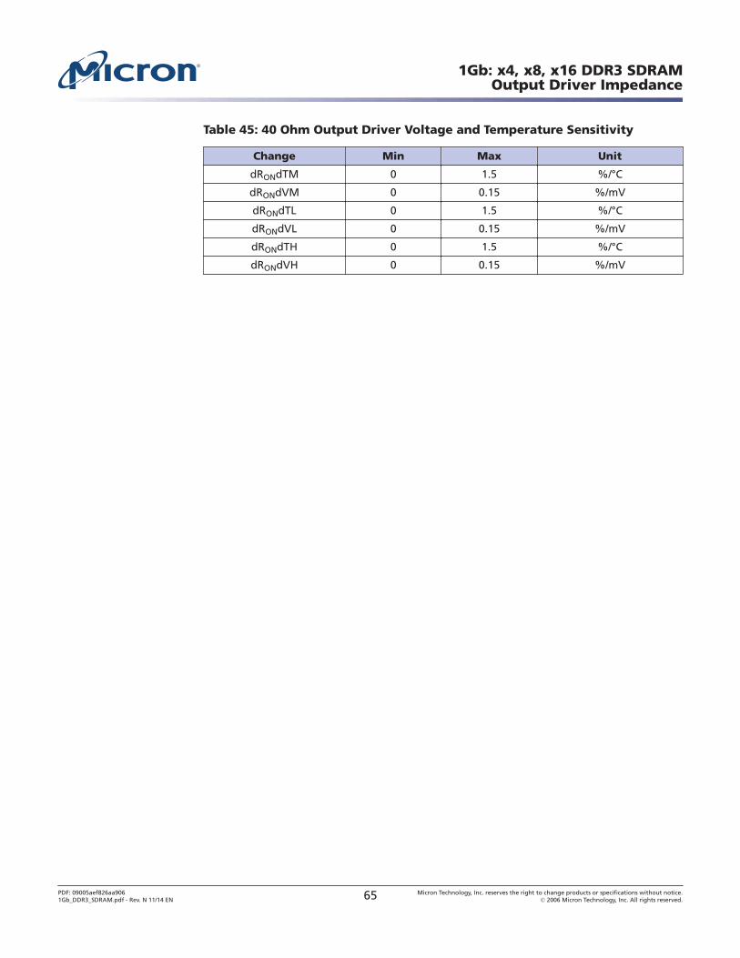
Table 45: 40 Ohm Output Driver Voltage and Temperature Sensitivity
Change Min Max Unit
dRONdTM 0 1.5 %/°C
dRONdVM 0 0.15 %/mV
dRONdTL 0 1.5 %/°C
dRONdVL 0 0.15 %/mV
dRONdTH 0 1.5 %/°C
dRONdVH 0 0.15 %/mV
1Gb: x4, x8, x16 DDR3 SDRAMOutput Driver Impedance
PDF: 09005aef826aa9061Gb_DDR3_SDRAM.pdf - Rev. N 11/14 EN 65 Micron Technology, Inc. reserves the right to change products or specifications without notice.
© 2006 Micron Technology, Inc. All rights reserved.
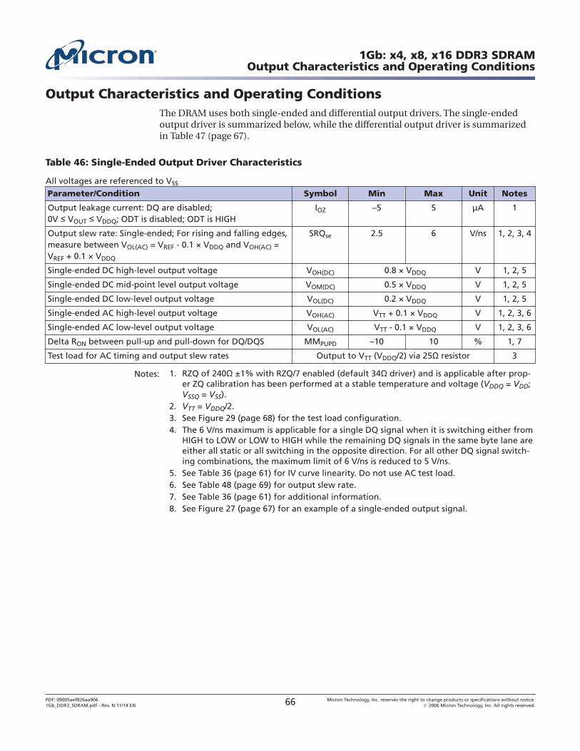
Output Characteristics and Operating ConditionsThe DRAM uses both single-ended and differential output drivers. The single-endedoutput driver is summarized below, while the differential output driver is summarizedin Table 47 (page 67).
Table 46: Single-Ended Output Driver Characteristics
All voltages are referenced to VSS
Parameter/Condition Symbol Min Max Unit Notes
Output leakage current: DQ are disabled;0V ≤ VOUT ≤ VDDQ; ODT is disabled; ODT is HIGH
IOZ –5 5 μA 1
Output slew rate: Single-ended; For rising and falling edges,measure between VOL(AC) = VREF - 0.1 × VDDQ and VOH(AC) =VREF + 0.1 × VDDQ
SRQse 2.5 6 V/ns 1, 2, 3, 4
Single-ended DC high-level output voltage VOH(DC) 0.8 × VDDQ V 1, 2, 5
Single-ended DC mid-point level output voltage VOM(DC) 0.5 × VDDQ V 1, 2, 5
Single-ended DC low-level output voltage VOL(DC) 0.2 × VDDQ V 1, 2, 5
Single-ended AC high-level output voltage VOH(AC) VTT + 0.1 × VDDQ V 1, 2, 3, 6
Single-ended AC low-level output voltage VOL(AC) VTT - 0.1 × VDDQ V 1, 2, 3, 6
Delta RON between pull-up and pull-down for DQ/DQS MMPUPD –10 10 % 1, 7
Test load for AC timing and output slew rates Output to VTT (VDDQ/2) via 25Ω resistor 3
Notes: 1. RZQ of 240Ω ±1% with RZQ/7 enabled (default 34Ω driver) and is applicable after prop-er ZQ calibration has been performed at a stable temperature and voltage (VDDQ = VDD;VSSQ = VSS).
2. VTT = VDDQ/2.3. See Figure 29 (page 68) for the test load configuration.4. The 6 V/ns maximum is applicable for a single DQ signal when it is switching either from
HIGH to LOW or LOW to HIGH while the remaining DQ signals in the same byte lane areeither all static or all switching in the opposite direction. For all other DQ signal switch-ing combinations, the maximum limit of 6 V/ns is reduced to 5 V/ns.
5. See Table 36 (page 61) for IV curve linearity. Do not use AC test load.6. See Table 48 (page 69) for output slew rate.7. See Table 36 (page 61) for additional information.8. See Figure 27 (page 67) for an example of a single-ended output signal.
1Gb: x4, x8, x16 DDR3 SDRAMOutput Characteristics and Operating Conditions
PDF: 09005aef826aa9061Gb_DDR3_SDRAM.pdf - Rev. N 11/14 EN 66 Micron Technology, Inc. reserves the right to change products or specifications without notice.
© 2006 Micron Technology, Inc. All rights reserved.
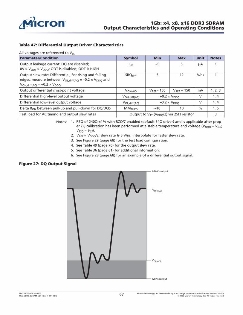
Table 47: Differential Output Driver Characteristics
All voltages are referenced to VSS
Parameter/Condition Symbol Min Max Unit Notes
Output leakage current: DQ are disabled;0V ≤ VOUT ≤ VDDQ; ODT is disabled; ODT is HIGH
IOZ –5 5 μA 1
Output slew rate: Differential; For rising and fallingedges, measure between VOL,diff(AC) = –0.2 × VDDQ andVOH,diff(AC) = +0.2 × VDDQ
SRQdiff 5 12 V/ns 1
Output differential cross-point voltage VOX(AC) VREF - 150 VREF + 150 mV 1, 2, 3
Differential high-level output voltage VOH,diff(AC) +0.2 × VDDQ V 1, 4
Differential low-level output voltage VOL,diff(AC) –0.2 × VDDQ V 1, 4
Delta RON between pull-up and pull-down for DQ/DQS MMPUPD –10 10 % 1, 5
Test load for AC timing and output slew rates Output to VTT (VDDQ/2) via 25Ω resistor 3
Notes: 1. RZQ of 240Ω ±1% with RZQ/7 enabled (default 34Ω driver) and is applicable after prop-er ZQ calibration has been performed at a stable temperature and voltage (VDDQ = VDD;VSSQ = VSS).
2. VREF = VDDQ/2; slew rate @ 5 V/ns, interpolate for faster slew rate.3. See Figure 29 (page 68) for the test load configuration.4. See Table 49 (page 70) for the output slew rate.5. See Table 36 (page 61) for additional information.6. See Figure 28 (page 68) for an example of a differential output signal.
Figure 27: DQ Output Signal
VOH(AC)
MIN output
MAX output
VOL(AC)
1Gb: x4, x8, x16 DDR3 SDRAMOutput Characteristics and Operating Conditions
PDF: 09005aef826aa9061Gb_DDR3_SDRAM.pdf - Rev. N 11/14 EN 67 Micron Technology, Inc. reserves the right to change products or specifications without notice.
© 2006 Micron Technology, Inc. All rights reserved.
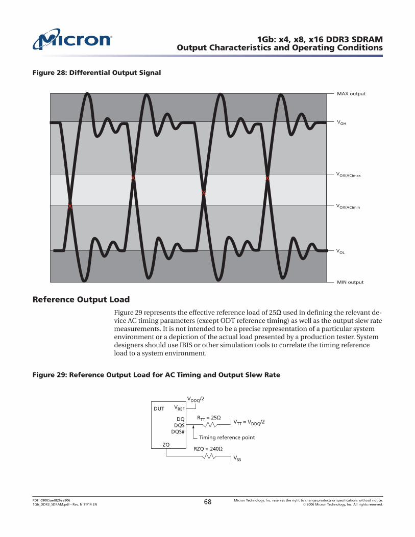
Figure 28: Differential Output Signal
VOH
MIN output
MAX output
VOL
VOX(AC)max
VOX(AC)minX
X
X
X
Reference Output Load
Figure 29 represents the effective reference load of 25Ω used in defining the relevant de-vice AC timing parameters (except ODT reference timing) as well as the output slew ratemeasurements. It is not intended to be a precise representation of a particular systemenvironment or a depiction of the actual load presented by a production tester. Systemdesigners should use IBIS or other simulation tools to correlate the timing referenceload to a system environment.
Figure 29: Reference Output Load for AC Timing and Output Slew Rate
Timing reference point
DQDQS
DQS#
DUT VREF
VTT = VDDQ/2
VDDQ/2
ZQRZQ = 240
VSS
RTT = 25
1Gb: x4, x8, x16 DDR3 SDRAMOutput Characteristics and Operating Conditions
PDF: 09005aef826aa9061Gb_DDR3_SDRAM.pdf - Rev. N 11/14 EN 68 Micron Technology, Inc. reserves the right to change products or specifications without notice.
© 2006 Micron Technology, Inc. All rights reserved.

Slew Rate Definitions for Single-Ended Output Signals
The single-ended output driver is summarized in Table 46 (page 66). With the referenceload for timing measurements, the output slew rate for falling and rising edges is de-fined and measured between VOL(AC) and VOH(AC) for single-ended signals.
Table 48: Single-Ended Output Slew Rate Definition
Single-Ended Output SlewRates (Linear Signals) Measured
CalculationOutput Edge From To
DQ Rising VOL(AC) VOH(AC) VOH(AC) - VOL(AC)
ΔTRse
Falling VOH(AC) VOL(AC) VOH(AC) - VOL(AC)
ΔTFse
Figure 30: Nominal Slew Rate Definition for Single-Ended Output Signals
VOH(AC)
VOL(AC)
VTT
ΔTFse
ΔTRse
1Gb: x4, x8, x16 DDR3 SDRAMOutput Characteristics and Operating Conditions
PDF: 09005aef826aa9061Gb_DDR3_SDRAM.pdf - Rev. N 11/14 EN 69 Micron Technology, Inc. reserves the right to change products or specifications without notice.
© 2006 Micron Technology, Inc. All rights reserved.
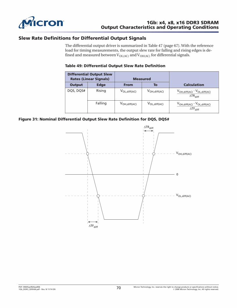
Slew Rate Definitions for Differential Output Signals
The differential output driver is summarized in Table 47 (page 67). With the referenceload for timing measurements, the output slew rate for falling and rising edges is de-fined and measured between VOL(AC) and VOH(AC) for differential signals.
Table 49: Differential Output Slew Rate Definition
Differential Output SlewRates (Linear Signals) Measured
CalculationOutput Edge From To
DQS, DQS# Rising VOL,diff(AC) VOH,diff(AC) VOH,diff(AC) - VOL,diff(AC)
ΔTRdiff
Falling VOH,diff(AC) VOL,diff(AC) VOH,diff(AC) - VOL,diff(AC)
ΔTFdiff
Figure 31: Nominal Differential Output Slew Rate Definition for DQS, DQS#
ΔTRdiff
ΔTFdiff
VOH,diff(AC)
VOL,diff(AC)
0
1Gb: x4, x8, x16 DDR3 SDRAMOutput Characteristics and Operating Conditions
PDF: 09005aef826aa9061Gb_DDR3_SDRAM.pdf - Rev. N 11/14 EN 70 Micron Technology, Inc. reserves the right to change products or specifications without notice.
© 2006 Micron Technology, Inc. All rights reserved.
Speed Bin Tables
Table 50: DDR3-1066 Speed Bins
DDR3-1066 Speed Bin -187E -187
Unit Notes
CL-tRCD-tRP 7-7-7 8-8-8
Parameter Symbol Min Max Min Max
Internal READ command to first data tAA 13.125 – 15 – ns
ACTIVATE to internal READ or WRITE delaytime
tRCD 13.125 – 15 – ns
PRECHARGE command period tRP 13.125 – 15 – ns
ACTIVATE-to-ACTIVATE or REFRESH commandperiod
tRC 50.625 – 52.5 – ns
ACTIVATE-to-PRECHARGE command period tRAS 37.5 9 x tREFI 37.5 9 x tREFI ns 1
CL = 5 CWL = 5 tCK (AVG) 3.0 3.3 3.0 3.3 ns 2
CWL = 6 tCK (AVG) Reserved Reserved ns 3
CL = 6 CWL = 5 tCK (AVG) 2.5 3.3 2.5 3.3 ns 2
CWL = 6 tCK (AVG) Reserved Reserved ns 3
CL = 7 CWL = 5 tCK (AVG) Reserved Reserved ns 3
CWL = 6 tCK (AVG) 1.875 <2.5 Reserved ns 2, 3
CL = 8 CWL = 5 tCK (AVG) Reserved Reserved ns 3
CWL = 6 tCK (AVG) 1.875 <2.5 1.875 <2.5 ns 2
Supported CL settings 5, 6, 7, 8 5, 6, 8 CK
Supported CWL settings 5, 6 5, 6 CK
Notes: 1. tREFI depends on TOPER.2. The CL and CWL settings result in tCK requirements. When making a selection of tCK,
both CL and CWL requirement settings need to be fulfilled.3. Reserved settings are not allowed.
1Gb: x4, x8, x16 DDR3 SDRAMSpeed Bin Tables
PDF: 09005aef826aa9061Gb_DDR3_SDRAM.pdf - Rev. N 11/14 EN 71 Micron Technology, Inc. reserves the right to change products or specifications without notice.
© 2006 Micron Technology, Inc. All rights reserved.
Table 51: DDR3-1333 Speed Bins
DDR3-1333 Speed Bin -15E1 -152
Unit Notes
CL-tRCD-tRP 9-9-9 10-10-10
Parameter Symbol Min Max Min Max
Internal READ command to first data tAA 13.5 – 15 – ns
ACTIVATE to internal READ or WRITE delaytime
tRCD 13.5 – 15 – ns
PRECHARGE command period tRP 13.5 – 15 – ns
ACTIVATE-to-ACTIVATE or REFRESH commandperiod
tRC 49.5 – 51 – ns
ACTIVATE-to-PRECHARGE command period tRAS 36 9 x tREFI 36 9 x tREFI ns 3
CL = 5 CWL = 5 tCK (AVG) 3.0 3.3 3.0 3.3 ns 4
CWL = 6, 7 tCK (AVG) Reserved Reserved ns 5
CL = 6 CWL = 5 tCK (AVG) 2.5 3.3 2.5 3.3 ns 4
CWL = 6 tCK (AVG) Reserved Reserved ns 5
CWL = 7 tCK (AVG) Reserved Reserved ns 5
CL = 7 CWL = 5 tCK (AVG) Reserved Reserved ns 5
CWL = 6 tCK (AVG) 1.875 <2.5 Reserved ns 4, 5
CWL = 7 tCK (AVG) Reserved Reserved ns 5
CL = 8 CWL = 5 tCK (AVG) Reserved Reserved ns 5
CWL = 6 tCK (AVG) 1.875 <2.5 1.875 <2.5 ns 4
CWL = 7 tCK (AVG) Reserved Reserved ns 5
CL = 9 CWL = 5, 6 tCK (AVG) Reserved Reserved ns 5
CWL = 7 tCK (AVG) 1.5 <1.875 Reserved ns 4, 5
CL = 10 CWL = 5, 6 tCK (AVG) Reserved Reserved ns 5
CWL = 7 tCK (AVG) 1.5 <1.875 1.5 <1.875 ns 4
Supported CL settings 5, 6, 7, 8, 9, 10 5, 6, 8, 10 CK
Supported CWL settings 5, 6, 7 5, 6, 7 CK
Notes: 1. The -15E speed grade is backward compatible with 1066, CL = 7 (-187E).2. The -15 speed grade is backward compatible with 1066, CL = 8 (-187).3. tREFI depends on TOPER.4. The CL and CWL settings result in tCK requirements. When making a selection of tCK,
both CL and CWL requirement settings need to be fulfilled.5. Reserved settings are not allowed.
1Gb: x4, x8, x16 DDR3 SDRAMSpeed Bin Tables
PDF: 09005aef826aa9061Gb_DDR3_SDRAM.pdf - Rev. N 11/14 EN 72 Micron Technology, Inc. reserves the right to change products or specifications without notice.
© 2006 Micron Technology, Inc. All rights reserved.
Table 52: DDR3-1600 Speed Bins
DDR3-1600 Speed Bin -1251
Unit Notes
CL-tRCD-tRP 11-11-11
Parameter Symbol Min Max
Internal READ command to first data tAA 13.75 – ns
ACTIVATE to internal READ or WRITE delay time tRCD 13.75 – ns
PRECHARGE command period tRP 13.75 – ns
ACTIVATE-to-ACTIVATE or REFRESH command period tRC 48.75 – ns
ACTIVATE-to-PRECHARGE command period tRAS 35 9 x tREFI ns 2
CL = 5 CWL = 5 tCK (AVG) 3.0 3.3 ns 3
CWL = 6, 7, 8 tCK (AVG) Reserved ns 4
CL = 6 CWL = 5 tCK (AVG) 2.5 3.3 ns 3
CWL = 6 tCK (AVG) Reserved ns 4
CWL = 7, 8 tCK (AVG) Reserved ns 4
CL = 7 CWL = 5 tCK (AVG) Reserved ns 4
CWL = 6 tCK (AVG) 1.875 <2.5 ns 3
CWL = 7 tCK (AVG) Reserved ns 4
CWL = 8 tCK (AVG) Reserved ns 4
CL = 8 CWL = 5 tCK (AVG) Reserved ns 4
CWL = 6 tCK (AVG) 1.875 <2.5 ns 3
CWL = 7 tCK (AVG) Reserved ns 4
CWL = 8 tCK (AVG) Reserved ns 4
CL = 9 CWL = 5, 6 tCK (AVG) Reserved ns 4
CWL = 7 tCK (AVG) 1.5 <1.875 ns 3
CWL = 8 tCK (AVG) Reserved ns 4
CL = 10 CWL = 5, 6 tCK (AVG) Reserved ns 4
CWL = 7 tCK (AVG) 1.5 <1.875 ns 3
CWL = 8 tCK (AVG) Reserved ns 4
CL = 11 CWL = 5, 6, 7 tCK (AVG) Reserved ns 4
CWL = 8 tCK (AVG) 1.25 <1.5 ns 3
Supported CL settings 5, 6, 7, 8, 9, 10, 11 CK
Supported CWL settings 5, 6, 7, 8 CK
Notes: 1. The -125 speed grade is backward compatible with 1333, CL = 9 (-15E) and 1066, CL = 7(-187E).
2. tREFI depends on TOPER.3. The CL and CWL settings result in tCK requirements. When making a selection of tCK,
both CL and CWL requirement settings need to be fulfilled.4. Reserved settings are not allowed.
1Gb: x4, x8, x16 DDR3 SDRAMSpeed Bin Tables
PDF: 09005aef826aa9061Gb_DDR3_SDRAM.pdf - Rev. N 11/14 EN 73 Micron Technology, Inc. reserves the right to change products or specifications without notice.
© 2006 Micron Technology, Inc. All rights reserved.
Table 53: DDR3-1866 Speed Bins
DDR3-1866 Speed Bin -1071
Unit Notes
CL-tRCD-tRP 13-13-13
Parameter Symbol Min Max
Internal READ command to first data tAA 13.91 20
ACTIVATE to internal READ or WRITE delay time tRCD 13.91 – ns
PRECHARGE command period tRP 13.91 – ns
ACTIVATE-to-ACTIVATE or REFRESH command period tRC 47.91 – ns
ACTIVATE-to-PRECHARGE command period tRAS 34 9 x tREFI ns 2
CL = 5 CWL = 5 tCK (AVG) 3.0 3.3 ns 3
CWL = 6, 7, 8, 9 tCK (AVG) Reserved ns 4
CL = 6 CWL = 5 tCK (AVG) 2.5 3.3 ns 3
CWL = 6, 7, 8, 9 tCK (AVG) Reserved ns 4
CL = 7 CWL = 5, 7, 8, 9 tCK (AVG) Reserved ns 4
CWL = 6 tCK (AVG) 1.875 <2.5 ns 3
CL = 8 CWL = 5, 8, 9 tCK (AVG) Reserved ns 4
CWL = 6 tCK (AVG) 1.875 <2.5 ns 3
CWL = 7 tCK (AVG) Reserved ns 4
CL = 9 CWL = 5, 6, 8, 9 tCK (AVG) Reserved ns 4
CWL = 7 tCK (AVG) 1.5 <1.875 ns 3
CL = 10 CWL = 5, 6, 9 tCK (AVG) Reserved ns 4
CWL = 7 tCK (AVG) 1.5 <1.875 ns 3
CWL = 8 tCK (AVG) Reserved ns 4
CL = 11 CWL = 5, 6, 7 tCK (AVG) Reserved ns 4
CWL = 8 tCK (AVG) 1.25 <1.5 ns 3
CWL = 9 tCK (AVG) Reserved ns 4
CL = 12 CWL = 5, 6, 7, 8 tCK (AVG) Reserved ns 4
CWL = 9 tCK (AVG) Reserved ns 4
CL = 13 CWL = 5, 6, 7, 8 tCK (AVG) Reserved ns 4
CWL = 9 tCK (AVG) 1.07 <1.25 ns 3
Supported CL settings 5, 6, 7, 8, 9, 10, 11, 13 CK
Supported CWL settings 5, 6, 7, 8, 9 CK
Notes: 1. The -107 speed grade is backward compatible with 1600, CL = 11 (-125); 1333, CL = 9(-15E); and 1066, CL = 7 (-187E).
2. tREFI depends on TOPER.3. The CL and CWL settings result in tCK requirements. When making a selection of tCK,
both CL and CWL requirement settings need to be fulfilled.4. Reserved settings are not allowed.
1Gb: x4, x8, x16 DDR3 SDRAMSpeed Bin Tables
PDF: 09005aef826aa9061Gb_DDR3_SDRAM.pdf - Rev. N 11/14 EN 74 Micron Technology, Inc. reserves the right to change products or specifications without notice.
© 2006 Micron Technology, Inc. All rights reserved.
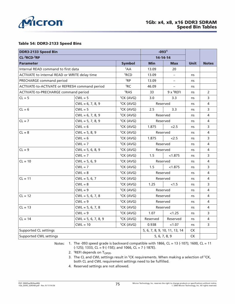
Table 54: DDR3-2133 Speed Bins
DDR3-2133 Speed Bin -0931
Unit Notes
CL-tRCD-tRP 14-14-14
Parameter Symbol Min Max
Internal READ command to first data tAA 13.09 20
ACTIVATE to internal READ or WRITE delay time tRCD 13.09 – ns
PRECHARGE command period tRP 13.09 – ns
ACTIVATE-to-ACTIVATE or REFRESH command period tRC 46.09 – ns
ACTIVATE-to-PRECHARGE command period tRAS 33 9 x tREFI ns 2
CL = 5 CWL = 5 tCK (AVG) 3.0 3.3 ns 3
CWL = 6, 7, 8, 9 tCK (AVG) Reserved ns 4
CL = 6 CWL = 5 tCK (AVG) 2.5 3.3 ns 3
CWL = 6, 7, 8, 9 tCK (AVG) Reserved ns 4
CL = 7 CWL = 5, 7, 8, 9 tCK (AVG) Reserved ns 4
CWL = 6 tCK (AVG) 1.875 <2.5 ns 3
CL = 8 CWL = 5, 8, 9 tCK (AVG) Reserved ns 4
CWL = 6 tCK (AVG) 1.875 <2.5 ns 3
CWL = 7 tCK (AVG) Reserved ns 4
CL = 9 CWL = 5, 6, 8, 9 tCK (AVG) Reserved ns 4
CWL = 7 tCK (AVG) 1.5 <1.875 ns 3
CL = 10 CWL = 5, 6, 9 tCK (AVG) Reserved ns 4
CWL = 7 tCK (AVG) 1.5 <1.875 ns 3
CWL = 8 tCK (AVG) Reserved ns 4
CL = 11 CWL = 5, 6, 7 tCK (AVG) Reserved ns 4
CWL = 8 tCK (AVG) 1.25 <1.5 ns 3
CWL = 9 tCK (AVG) Reserved ns 4
CL = 12 CWL = 5, 6, 7, 8 tCK (AVG) Reserved ns 4
CWL = 9 tCK (AVG) Reserved ns 4
CL = 13 CWL = 5, 6, 7, 8 tCK (AVG) Reserved ns 4
CWL = 9 tCK (AVG) 1.07 <1.25 ns 3
CL = 14 CWL = 5, 6, 7, 8, 9 tCK (AVG) Reserved Reserved ns 4
CWL = 10 tCK (AVG) 0.938 <1.07 ns 3
Supported CL settings 5, 6, 7, 8, 9, 10, 11, 13, 14 CK
Supported CWL settings 5, 6, 7, 8, 9 CK
Notes: 1. The -093 speed grade is backward compatible with 1866, CL = 13 (-107); 1600, CL = 11(-125); 1333, CL = 9 (-15E); and 1066, CL = 7 (-187E).
2. tREFI depends on TOPER.3. The CL and CWL settings result in tCK requirements. When making a selection of tCK,
both CL and CWL requirement settings need to be fulfilled.4. Reserved settings are not allowed.
1Gb: x4, x8, x16 DDR3 SDRAMSpeed Bin Tables
PDF: 09005aef826aa9061Gb_DDR3_SDRAM.pdf - Rev. N 11/14 EN 75 Micron Technology, Inc. reserves the right to change products or specifications without notice.
© 2006 Micron Technology, Inc. All rights reserved.
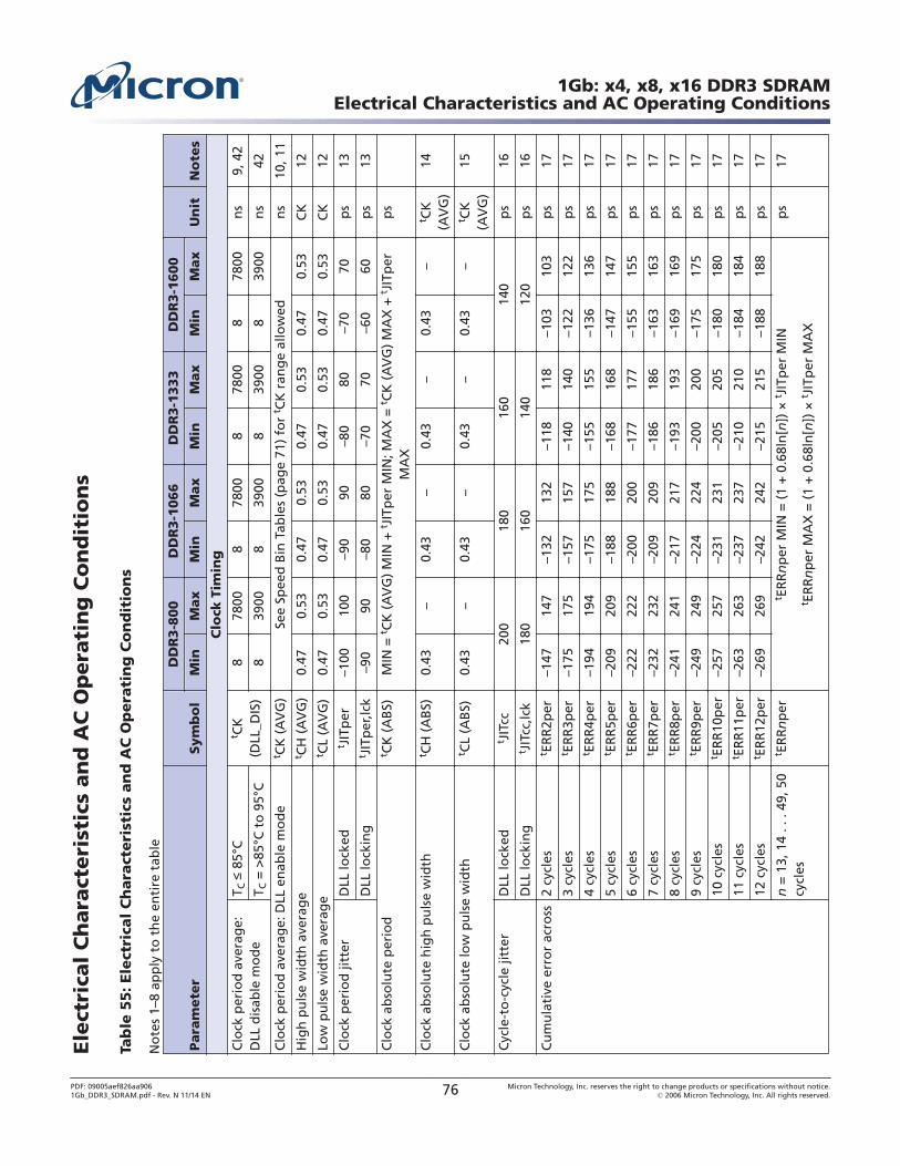
Ele
ctri
cal
Ch
ara
cteri
stic
s an
d A
C O
pera
tin
g C
on
dit
ion
s
Tab
le 5
5: Ele
ctri
cal
Ch
ara
cteri
stic
s an
d A
C O
pera
tin
g C
on
dit
ion
s
No
tes
1–8
app
ly t
o t
he
enti
re t
able
Para
mete
rSym
bo
l
DD
R3-8
00
DD
R3-1
066
DD
R3-1
333
DD
R3-1
600
Un
itN
ote
sM
inM
ax
Min
Max
Min
Max
Min
Max
Clo
ck T
imin
g
Clo
ck p
erio
d a
vera
ge:
DLL
dis
able
mo
de
T C ≤
85°
Ct C
K(D
LL_D
IS)
878
008
7800
878
008
7800
ns
9, 4
2
T C =
>85
°C t
o 9
5°C
839
008
3900
839
008
3900
ns
42
Clo
ck p
erio
d a
vera
ge:
DLL
en
able
mo
de
t CK
(A
VG
)Se
e Sp
eed
Bin
Tab
les
(pag
e 71
) fo
r t C
K r
ang
e al
low
edn
s10
, 11
Hig
h p
uls
e w
idth
ave
rag
et C
H (
AV
G)
0.47
0.53
0.47
0.53
0.47
0.53
0.47
0.53
CK
12
Low
pu
lse
wid
th a
vera
ge
t CL
(AV
G)
0.47
0.53
0.47
0.53
0.47
0.53
0.47
0.53
CK
12
Clo
ck p
erio
d ji
tter
DLL
lock
edt J
ITp
er–1
0010
0–9
090
–80
80–7
070
ps
13
DLL
lock
ing
t JIT
per
,lck
–90
90–8
080
–70
70–6
060
ps
13
Clo
ck a
bso
lute
per
iod
t CK
(A
BS)
MIN
= t C
K (
AV
G)
MIN
+ t J
ITp
er M
IN; M
AX
= t C
K (
AV
G)
MA
X +
t JIT
per
MA
Xp
s
Clo
ck a
bso
lute
hig
h p
uls
e w
idth
t CH
(A
BS)
0.43
–0.
43–
0.43
–0.
43–
t CK
(AV
G)
14
Clo
ck a
bso
lute
low
pu
lse
wid
tht C
L (A
BS)
0.43
–0.
43–
0.43
–0.
43–
t CK
(AV
G)
15
Cyc
le-t
o-c
ycle
jitt
erD
LL lo
cked
t JIT
cc20
018
016
014
0p
s16
DLL
lock
ing
t JIT
cc,lc
k18
016
014
012
0p
s16
Cu
mu
lati
ve e
rro
r ac
ross
2 cy
cles
t ER
R2p
er–1
4714
7–1
3213
2–1
1811
8–1
0310
3p
s17
3 cy
cles
t ER
R3p
er–1
7517
5–1
5715
7–1
4014
0–1
2212
2p
s17
4 cy
cles
t ER
R4p
er–1
9419
4–1
7517
5–1
5515
5–1
3613
6p
s17
5 cy
cles
t ER
R5p
er–2
0920
9–1
8818
8–1
6816
8–1
4714
7p
s17
6 cy
cles
t ER
R6p
er–2
2222
2–2
0020
0–1
7717
7–1
5515
5p
s17
7 cy
cles
t ER
R7p
er–2
3223
2–2
0920
9–1
8618
6–1
6316
3p
s17
8 cy
cles
t ER
R8p
er–2
4124
1–2
1721
7–1
9319
3–1
6916
9p
s17
9 cy
cles
t ER
R9p
er–2
4924
9–2
2422
4–2
0020
0–1
7517
5p
s17
10 c
ycle
st E
RR
10p
er–2
5725
7–2
3123
1–2
0520
5–1
8018
0p
s17
11 c
ycle
st E
RR
11p
er–2
6326
3–2
3723
7–2
1021
0–1
8418
4p
s17
12 c
ycle
st E
RR
12p
er–2
6926
9–2
4224
2–2
1521
5–1
8818
8p
s17
n =
13,
14
. . .
49, 5
0cy
cles
t ER
Rn
per
t ER
Rn
per
MIN
= (
1 +
0.6
8ln
[n])
× t J
ITp
er M
IN
t ER
Rn
per
MA
X =
(1
+ 0
.68l
n[n
]) ×
t JIT
per
MA
X
ps
17
1Gb: x4, x8, x16 DDR3 SDRAMElectrical Characteristics and AC Operating Conditions
PDF: 09005aef826aa9061Gb_DDR3_SDRAM.pdf - Rev. N 11/14 EN 76 Micron Technology, Inc. reserves the right to change products or specifications without notice.
© 2006 Micron Technology, Inc. All rights reserved.
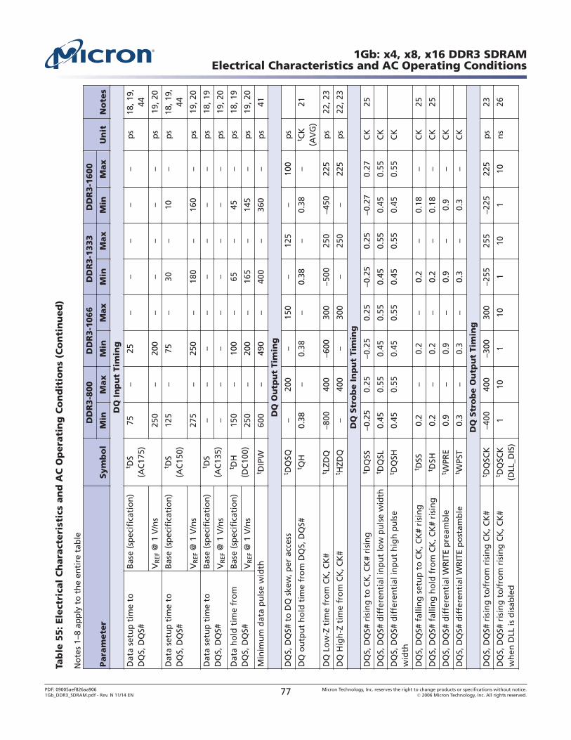
Tab
le 5
5: Ele
ctri
cal
Ch
ara
cteri
stic
s an
d A
C O
pera
tin
g C
on
dit
ion
s (C
on
tin
ued
)
No
tes
1–8
app
ly t
o t
he
enti
re t
able
Para
mete
rSym
bo
l
DD
R3-8
00
DD
R3-1
066
DD
R3-1
333
DD
R3-1
600
Un
itN
ote
sM
inM
ax
Min
Max
Min
Max
Min
Max
DQ
In
pu
t Ti
min
g
Dat
a se
tup
tim
e to
DQ
S, D
QS#
Bas
e (s
pec
ific
atio
n)
t DS
(AC
175)
75–
25–
––
––
ps
18, 1
9,44
VR
EF @
1 V
/ns
250
–20
0–
––
––
ps
19, 2
0
Dat
a se
tup
tim
e to
DQ
S, D
QS#
Bas
e (s
pec
ific
atio
n)
t DS
(AC
150)
125
–75
–30
–10
–p
s18
, 19,
44
VR
EF @
1 V
/ns
275
–25
0–
180
–16
0–
ps
19, 2
0
Dat
a se
tup
tim
e to
DQ
S, D
QS#
Bas
e (s
pec
ific
atio
n)
t DS
(AC
135)
––
––
––
––
ps
18, 1
9
VR
EF @
1 V
/ns
––
––
––
––
ps
19, 2
0
Dat
a h
old
tim
e fr
om
DQ
S, D
QS#
Bas
e (s
pec
ific
atio
n)
t DH
(DC
100)
150
–10
0–
65–
45–
ps
18, 1
9
VR
EF @
1 V
/ns
250
–20
0–
165
–14
5–
ps
19, 2
0
Min
imu
m d
ata
pu
lse
wid
tht D
IPW
600
–49
0–
400
–36
0–
ps
41
DQ
Ou
tpu
t Ti
min
g
DQ
S, D
QS#
to
DQ
ske
w, p
er a
cces
st D
QSQ
–20
0–
150
–12
5–
100
ps
DQ
ou
tpu
t h
old
tim
e fr
om
DQ
S, D
QS#
t QH
0.38
–0.
38–
0.38
–0.
38–
t CK
(AV
G)
21
DQ
Lo
w-Z
tim
e fr
om
CK
, CK
#t L
ZDQ
–800
400
–600
300
–500
250
–450
225
ps
22, 2
3
DQ
Hig
h-Z
tim
e fr
om
CK
, CK
#t H
ZDQ
–40
0–
300
–25
0–
225
ps
22, 2
3
DQ
Str
ob
e I
np
ut
Tim
ing
DQ
S, D
QS#
ris
ing
to
CK
, CK
# ri
sin
gt D
QSS
–0.2
50.
25–0
.25
0.25
–0.2
50.
25–0
.27
0.27
CK
25
DQ
S, D
QS#
dif
fere
nti
al in
pu
t lo
w p
uls
e w
idth
t DQ
SL0.
450.
550.
450.
550.
450.
550.
450.
55C
K
DQ
S, D
QS#
dif
fere
nti
al in
pu
t h
igh
pu
lse
wid
th
t DQ
SH0.
450.
550.
450.
550.
450.
550.
450.
55C
K
DQ
S, D
QS#
fal
ling
set
up
to
CK
, CK
# ri
sin
gt D
SS0.
2–
0.2
–0.
2–
0.18
–C
K25
DQ
S, D
QS#
fal
ling
ho
ld f
rom
CK
, CK
# ri
sin
gt D
SH0.
2–
0.2
–0.
2–
0.18
–C
K25
DQ
S, D
QS#
dif
fere
nti
al W
RIT
E p
ream
ble
t WPR
E0.
9–
0.9
–0.
9–
0.9
–C
K
DQ
S, D
QS#
dif
fere
nti
al W
RIT
E p
ost
amb
let W
PST
0.3
–0.
3–
0.3
–0.
3–
CK
DQ
Str
ob
e O
utp
ut
Tim
ing
DQ
S, D
QS#
ris
ing
to
/fro
m r
isin
g C
K, C
K#
t DQ
SCK
–400
400
–300
300
–255
255
–225
225
ps
23
DQ
S, D
QS#
ris
ing
to
/fro
m r
isin
g C
K, C
K#
wh
en D
LL is
dis
able
d
t DQ
SCK
(DLL
_DIS
)1
101
101
101
10n
s26
1Gb: x4, x8, x16 DDR3 SDRAMElectrical Characteristics and AC Operating Conditions
PDF: 09005aef826aa9061Gb_DDR3_SDRAM.pdf - Rev. N 11/14 EN 77 Micron Technology, Inc. reserves the right to change products or specifications without notice.
© 2006 Micron Technology, Inc. All rights reserved.
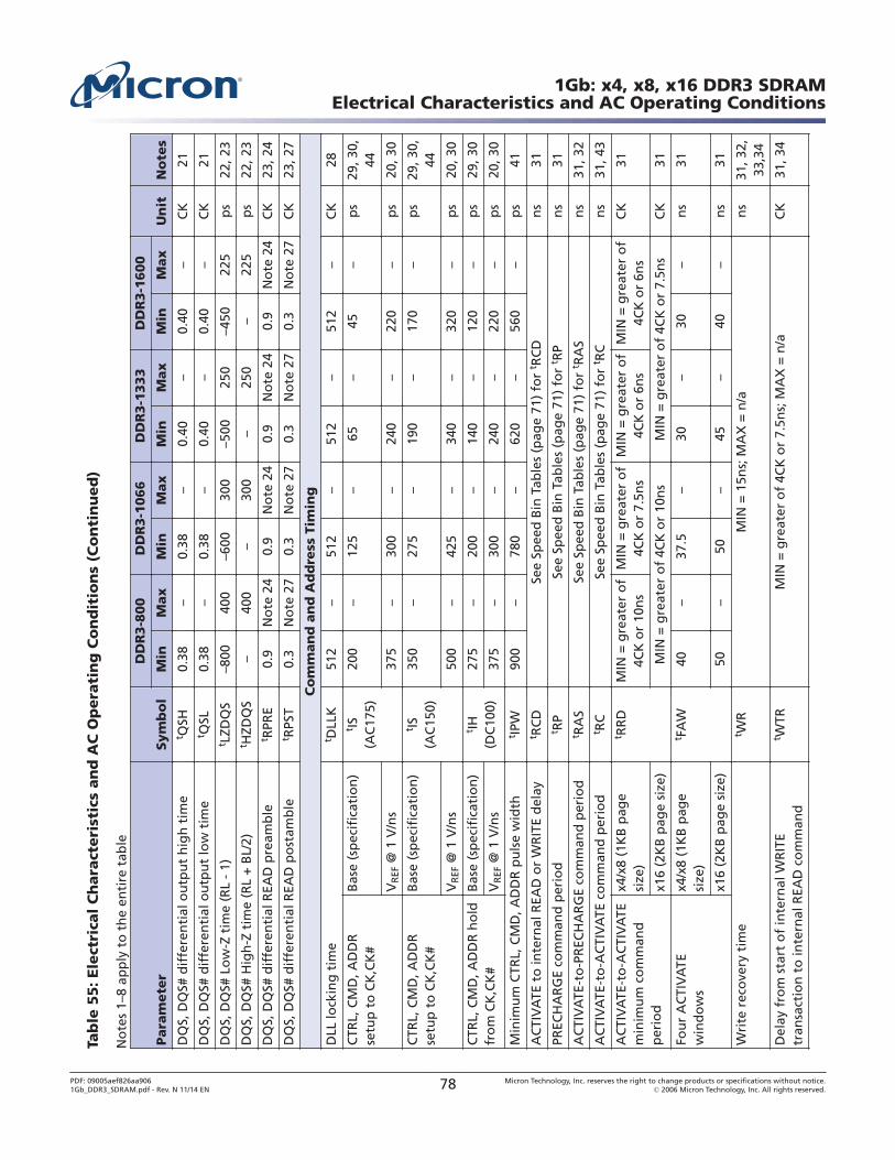
Tab
le 5
5: Ele
ctri
cal
Ch
ara
cteri
stic
s an
d A
C O
pera
tin
g C
on
dit
ion
s (C
on
tin
ued
)
No
tes
1–8
app
ly t
o t
he
enti
re t
able
Para
mete
rSym
bo
l
DD
R3-8
00
DD
R3-1
066
DD
R3-1
333
DD
R3-1
600
Un
itN
ote
sM
inM
ax
Min
Max
Min
Max
Min
Max
DQ
S, D
QS#
dif
fere
nti
al o
utp
ut
hig
h t
ime
t QSH
0.38
–0.
38–
0.40
–0.
40–
CK
21
DQ
S, D
QS#
dif
fere
nti
al o
utp
ut
low
tim
et Q
SL0.
38–
0.38
–0.
40–
0.40
–C
K21
DQ
S, D
QS#
Lo
w-Z
tim
e (R
L -
1)t L
ZDQ
S–8
0040
0–6
0030
0–5
0025
0–4
5022
5p
s22
, 23
DQ
S, D
QS#
Hig
h-Z
tim
e (R
L +
BL/
2)t H
ZDQ
S–
400
–30
0–
250
–22
5p
s22
, 23
DQ
S, D
QS#
dif
fere
nti
al R
EAD
pre
amb
let R
PRE
0.9
No
te 2
40.
9N
ote
24
0.9
No
te 2
40.
9N
ote
24
CK
23, 2
4
DQ
S, D
QS#
dif
fere
nti
al R
EAD
po
stam
ble
t RPS
T0.
3N
ote
27
0.3
No
te 2
70.
3N
ote
27
0.3
No
te 2
7C
K23
, 27
Co
mm
an
d a
nd
Ad
dre
ss T
imin
g
DLL
lock
ing
tim
et D
LLK
512
–51
2–
512
–51
2–
CK
28
CTR
L, C
MD
, AD
DR
setu
p t
o C
K,C
K#
Bas
e (s
pec
ific
atio
n)
t IS(A
C17
5)20
0–
125
–65
–45
–p
s29
, 30,
44
VR
EF @
1 V
/ns
375
–30
0–
240
–22
0–
ps
20, 3
0
CTR
L, C
MD
, AD
DR
setu
p t
o C
K,C
K#
Bas
e (s
pec
ific
atio
n)
t IS(A
C15
0)35
0–
275
–19
0–
170
–p
s29
, 30,
44
VR
EF @
1 V
/ns
500
–42
5–
340
–32
0–
ps
20, 3
0
CTR
L, C
MD
, AD
DR
ho
ldfr
om
CK
,CK
#B
ase
(sp
ecif
icat
ion
)t IH
(DC
100)
275
–20
0–
140
–12
0–
ps
29, 3
0
VR
EF @
1 V
/ns
375
–30
0–
240
–22
0–
ps
20, 3
0
Min
imu
m C
TRL,
CM
D, A
DD
R p
uls
e w
idth
t IPW
900
–78
0–
620
–56
0–
ps
41
AC
TIV
ATE
to
inte
rnal
REA
D o
r W
RIT
E d
elay
t RC
DSe
e Sp
eed
Bin
Tab
les
(pag
e 71
) fo
r t R
CD
ns
31
PREC
HA
RG
E co
mm
and
per
iod
t RP
See
Spee
d B
in T
able
s (p
age
71)
for
t RP
ns
31
AC
TIV
ATE
-to
-PR
ECH
AR
GE
com
man
d p
erio
dt R
AS
See
Spee
d B
in T
able
s (p
age
71)
for
t RA
Sn
s31
, 32
AC
TIV
ATE
-to
-AC
TIV
ATE
co
mm
and
per
iod
t RC
See
Spee
d B
in T
able
s (p
age
71)
for
t RC
ns
31, 4
3
AC
TIV
ATE
-to
-AC
TIV
ATE
min
imu
m c
om
man
dp
erio
d
x4/x
8 (1
KB
pag
esi
ze)
t RR
DM
IN =
gre
ater
of
4CK
or
10n
sM
IN =
gre
ater
of
4CK
or
7.5n
sM
IN =
gre
ater
of
4CK
or
6ns
MIN
= g
reat
er o
f4C
K o
r 6n
sC
K31
x16
(2K
B p
age
size
)M
IN =
gre
ater
of
4CK
or
10n
sM
IN =
gre
ater
of
4CK
or
7.5n
sC
K31
Fou
r A
CTI
VA
TEw
ind
ow
sx4
/x8
(1K
B p
age
size
)
t FA
W40
–37
.5–
30–
30–
ns
31
x16
(2K
B p
age
size
)50
–50
–45
–40
–n
s31
Wri
te r
eco
very
tim
et W
RM
IN =
15n
s; M
AX
= n
/an
s31
, 32,
33,3
4
Del
ay f
rom
sta
rt o
f in
tern
al W
RIT
Etr
ansa
ctio
n t
o in
tern
al R
EAD
co
mm
and
t WTR
MIN
= g
reat
er o
f 4C
K o
r 7.
5ns;
MA
X =
n/a
CK
31, 3
4
1Gb: x4, x8, x16 DDR3 SDRAMElectrical Characteristics and AC Operating Conditions
PDF: 09005aef826aa9061Gb_DDR3_SDRAM.pdf - Rev. N 11/14 EN 78 Micron Technology, Inc. reserves the right to change products or specifications without notice.
© 2006 Micron Technology, Inc. All rights reserved.
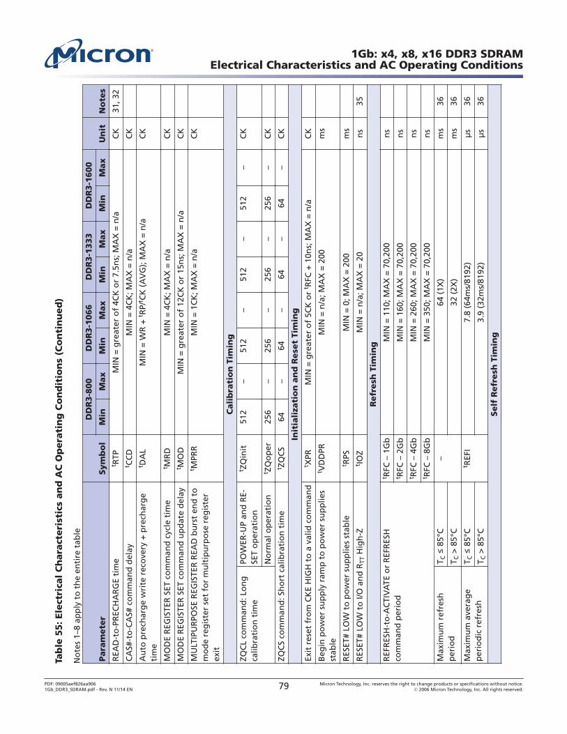
Tab
le 5
5: Ele
ctri
cal
Ch
ara
cteri
stic
s an
d A
C O
pera
tin
g C
on
dit
ion
s (C
on
tin
ued
)
No
tes
1–8
app
ly t
o t
he
enti
re t
able
Para
mete
rSym
bo
l
DD
R3-8
00
DD
R3-1
066
DD
R3-1
333
DD
R3-1
600
Un
itN
ote
sM
inM
ax
Min
Max
Min
Max
Min
Max
REA
D-t
o-P
REC
HA
RG
E ti
me
t RTP
MIN
= g
reat
er o
f 4C
K o
r 7.
5ns;
MA
X =
n/a
CK
31, 3
2
CA
S#-t
o-C
AS#
co
mm
and
del
ayt C
CD
MIN
= 4
CK
; MA
X =
n/a
CK
Au
to p
rech
arg
e w
rite
rec
ove
ry +
pre
char
ge
tim
e
t DA
LM
IN =
WR
+ t R
P/t C
K (
AV
G);
MA
X =
n/a
CK
MO
DE
REG
ISTE
R S
ET c
om
man
d c
ycle
tim
et M
RD
MIN
= 4
CK
; MA
X =
n/a
CK
MO
DE
REG
ISTE
R S
ET c
om
man
d u
pd
ate
del
ayt M
OD
MIN
= g
reat
er o
f 12
CK
or
15n
s; M
AX
= n
/aC
K
MU
LTIP
UR
POSE
REG
ISTE
R R
EAD
bu
rst
end
to
mo
de
reg
iste
r se
t fo
r m
ult
ipu
rpo
se r
egis
ter
exit
t MPR
RM
IN =
1C
K; M
AX
= n
/aC
K
Cali
bra
tio
n T
imin
g
ZQC
L co
mm
and
: Lo
ng
calib
rati
on
tim
ePO
WER
-UP
and
RE-
SET
op
erat
ion
t ZQ
init
512
–51
2–
512
–51
2–
CK
No
rmal
op
erat
ion
t ZQ
op
er25
6–
256
–25
6–
256
–C
K
ZQC
S co
mm
and
: Sh
ort
cal
ibra
tio
n t
ime
t ZQ
CS
64–
64–
64–
64–
CK
Init
iali
zati
on
an
d R
ese
t Ti
min
g
Exit
res
et f
rom
CK
E H
IGH
to
a v
alid
co
mm
and
t XPR
MIN
= g
reat
er o
f 5C
K o
r t R
FC +
10n
s; M
AX
= n
/aC
K
Beg
in p
ow
er s
up
ply
ram
p t
o p
ow
er s
up
plie
sst
able
t VD
DPR
MIN
= n
/a; M
AX
= 2
00m
s
RES
ET#
LOW
to
po
wer
su
pp
lies
stab
let R
PSM
IN =
0; M
AX
= 2
00m
s
RES
ET#
LOW
to
I/O
an
d R
TT H
igh
-Zt IO
ZM
IN =
n/a
; MA
X =
20
ns
35
Refr
esh
Tim
ing
REF
RES
H-t
o-A
CTI
VA
TE o
r R
EFR
ESH
com
man
d p
erio
d
t RFC
– 1
Gb
MIN
= 1
10; M
AX
= 7
0,20
0n
s
t RFC
– 2
Gb
MIN
= 1
60; M
AX
= 7
0,20
0n
s
t RFC
– 4
Gb
MIN
= 2
60; M
AX
= 7
0,20
0n
s
t RFC
– 8
Gb
MIN
= 3
50; M
AX
= 7
0,20
0n
s
Max
imu
m r
efre
shp
erio
dT C
≤ 8
5°C
–64
(1X
)m
s36
T C >
85°
C32
(2X
)m
s36
Max
imu
m a
vera
ge
per
iod
ic r
efre
shT C
≤ 8
5°C
t REF
I7.
8 (6
4ms/
8192
)μ
s36
T C >
85°
C3.
9 (3
2ms/
8192
)μ
s36
Self
Refr
esh
Tim
ing
1Gb: x4, x8, x16 DDR3 SDRAMElectrical Characteristics and AC Operating Conditions
PDF: 09005aef826aa9061Gb_DDR3_SDRAM.pdf - Rev. N 11/14 EN 79 Micron Technology, Inc. reserves the right to change products or specifications without notice.
© 2006 Micron Technology, Inc. All rights reserved.
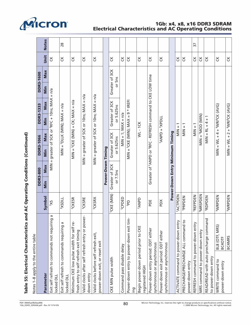
Tab
le 5
5: Ele
ctri
cal
Ch
ara
cteri
stic
s an
d A
C O
pera
tin
g C
on
dit
ion
s (C
on
tin
ued
)
No
tes
1–8
app
ly t
o t
he
enti
re t
able
Para
mete
rSym
bo
l
DD
R3-8
00
DD
R3-1
066
DD
R3-1
333
DD
R3-1
600
Un
itN
ote
sM
inM
ax
Min
Max
Min
Max
Min
Max
Exit
sel
f re
fres
h t
o c
om
man
ds
no
t re
qu
irin
g a
lock
ed D
LL
t XS
MIN
= g
reat
er o
f 5C
K o
r t R
FC +
10n
s; M
AX
= n
/aC
K
Exit
sel
f re
fres
h t
o c
om
man
ds
req
uir
ing
alo
cked
DLL
t XSD
LLM
IN =
t DLL
K (
MIN
); M
AX
= n
/aC
K28
Min
imu
m C
KE
low
pu
lse
wid
th f
or
self
re-
fres
h e
ntr
y to
sel
f re
fres
h e
xit
tim
ing
t CK
ESR
MIN
= t C
KE
(MIN
) +
CK
; MA
X =
n/a
CK
Val
id c
lock
s af
ter
self
ref
resh
en
try
or
po
wer
-d
ow
n e
ntr
y
t CK
SRE
MIN
= g
reat
er o
f 5C
K o
r 10
ns;
MA
X =
n/a
CK
Val
id c
lock
s b
efo
re s
elf
refr
esh
exi
t,p
ow
er-d
ow
n e
xit,
or
rese
t ex
it
t CK
SRX
MIN
= g
reat
er o
f 5C
K o
r 10
ns;
MA
X =
n/a
CK
Po
wer-
Do
wn
Tim
ing
CK
E M
IN p
uls
e w
idth
t CK
E (M
IN)
Gre
ater
of
3CK
or
7.5n
sG
reat
er o
f 3C
Ko
r 5.
625n
sG
reat
er o
f 3C
Ko
r 5.
625n
sG
reat
er o
f 3C
Ko
r 5n
sC
K
Co
mm
and
pas
s d
isab
le d
elay
t CPD
EDM
IN =
1; M
AX
= n
/aC
K
Pow
er-d
ow
n e
ntr
y to
po
wer
-do
wn
exi
t ti
m-
ing
t PD
MIN
= t C
KE
(MIN
); M
AX
= 9
* t
REF
IC
K
Beg
in p
ow
er-d
ow
n p
erio
d p
rio
r to
CK
Ere
gis
tere
d H
IGH
t AN
PDW
L -
1CK
CK
Pow
er-d
ow
n e
ntr
y p
erio
d: O
DT
eith
ersy
nch
ron
ou
s o
r as
ynch
ron
ou
sPD
EG
reat
er o
f t A
NPD
or
t RFC
- R
EFR
ESH
co
mm
and
to
CK
E LO
W t
ime
CK
Pow
er-d
ow
n e
xit
per
iod
: OD
T ei
ther
syn
chro
no
us
or
asyn
chro
no
us
PDX
t AN
PD +
t XPD
LLC
K
Po
wer-
Do
wn
En
try M
inim
um
Tim
ing
AC
TIV
ATE
co
mm
and
to
po
wer
-do
wn
en
try
t AC
TPD
ENM
IN =
1C
K
PREC
HA
RG
E/PR
ECH
AR
GE
ALL
co
mm
and
to
po
wer
-do
wn
en
try
t PR
PDEN
MIN
= 1
CK
REF
RES
H c
om
man
d t
o p
ow
er-d
ow
n e
ntr
yt R
EFPD
ENM
IN =
1C
K37
MR
S co
mm
and
to
po
wer
-do
wn
en
try
t MR
SPD
ENM
IN =
t MO
D (
MIN
)C
K
REA
D/R
EAD
wit
h a
uto
pre
char
ge
com
man
dto
po
wer
-do
wn
en
try
t RD
PDEN
MIN
= R
L +
4 +
1C
K
WR
ITE
com
man
d t
op
ow
er-d
ow
n e
ntr
yB
L8 (
OTF
, MR
S)B
C4O
TF
t WR
PDEN
MIN
= W
L +
4 +
t WR
/t CK
(A
VG
)C
K
BC
4MR
St W
RPD
ENM
IN =
WL
+ 2
+ t W
R/t C
K (
AV
G)
CK
1Gb: x4, x8, x16 DDR3 SDRAMElectrical Characteristics and AC Operating Conditions
PDF: 09005aef826aa9061Gb_DDR3_SDRAM.pdf - Rev. N 11/14 EN 80 Micron Technology, Inc. reserves the right to change products or specifications without notice.
© 2006 Micron Technology, Inc. All rights reserved.
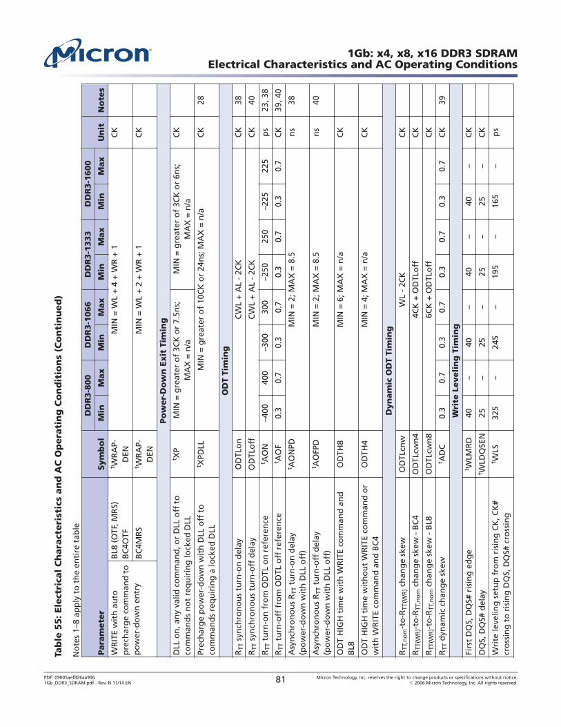
Tab
le 5
5: Ele
ctri
cal
Ch
ara
cteri
stic
s an
d A
C O
pera
tin
g C
on
dit
ion
s (C
on
tin
ued
)
No
tes
1–8
app
ly t
o t
he
enti
re t
able
Para
mete
rSym
bo
l
DD
R3-8
00
DD
R3-1
066
DD
R3-1
333
DD
R3-1
600
Un
itN
ote
sM
inM
ax
Min
Max
Min
Max
Min
Max
WR
ITE
wit
h a
uto
pre
char
ge
com
man
d t
op
ow
er-d
ow
n e
ntr
y
BL8
(O
TF, M
RS)
BC
4OTF
t WR
AP-
DEN
MIN
= W
L +
4 +
WR
+ 1
CK
BC
4MR
St W
RA
P-D
ENM
IN =
WL
+ 2
+ W
R +
1C
K
Po
wer-
Do
wn
Exit
Tim
ing
DLL
on
, an
y va
lid c
om
man
d, o
r D
LL o
ff t
oco
mm
and
s n
ot
req
uir
ing
lock
ed D
LL
t XP
MIN
= g
reat
er o
f 3C
K o
r 7.
5ns;
MA
X =
n/a
MIN
= g
reat
er o
f 3C
K o
r 6n
s;M
AX
= n
/aC
K
Prec
har
ge
po
wer
-do
wn
wit
h D
LL o
ff t
oco
mm
and
s re
qu
irin
g a
lock
ed D
LL
t XPD
LLM
IN =
gre
ater
of
10C
K o
r 24
ns;
MA
X =
n/a
CK
28
OD
T Ti
min
g
RTT
syn
chro
no
us
turn
-on
del
ayO
DTL
on
CW
L +
AL
- 2C
KC
K38
RTT
syn
chro
no
us
turn
-off
del
ayO
DTL
off
CW
L +
AL
- 2C
KC
K40
RTT
tu
rn-o
n f
rom
OD
TL o
n r
efer
ence
t AO
N–4
0040
0–3
0030
0–2
5025
0–2
2522
5p
s23
, 38
RTT
tu
rn-o
ff f
rom
OD
TL o
ff r
efer
ence
t AO
F0.
30.
70.
30.
70.
30.
70.
30.
7C
K39
, 40
Asy
nch
ron
ou
s R
TT t
urn
-on
del
ay(p
ow
er-d
ow
n w
ith
DLL
off
)
t AO
NPD
MIN
= 2
; MA
X =
8.5
ns
38
Asy
nch
ron
ou
s R
TT t
urn
-off
del
ay(p
ow
er-d
ow
n w
ith
DLL
off
)
t AO
FPD
MIN
= 2
; MA
X =
8.5
ns
40
OD
T H
IGH
tim
e w
ith
WR
ITE
com
man
d a
nd
BL8
OD
TH8
MIN
= 6
; MA
X =
n/a
CK
OD
T H
IGH
tim
e w
ith
ou
t W
RIT
E co
mm
and
or
wit
h W
RIT
E co
mm
and
an
d B
C4
OD
TH4
MIN
= 4
; MA
X =
n/a
CK
Dyn
am
ic O
DT
Tim
ing
RTT
,no
m-t
o-R
TT(W
R) c
han
ge
skew
OD
TLcn
wW
L -
2CK
CK
RTT
(WR
)-to
-RTT
,no
m c
han
ge
skew
- B
C4
OD
TLcw
n4
4CK
+ O
DTL
off
CK
RTT
(WR
)-to
-RTT
,no
m c
han
ge
skew
- B
L8O
DTL
cwn
86C
K +
OD
TLo
ffC
K
RTT
dyn
amic
ch
ang
e sk
ewt A
DC
0.3
0.7
0.3
0.7
0.3
0.7
0.3
0.7
CK
39
Wri
te L
eveli
ng
Tim
ing
Firs
t D
QS,
DQ
S# r
isin
g e
dg
et W
LMR
D40
–40
–40
–40
–C
K
DQ
S, D
QS#
del
ayt W
LDQ
SEN
25–
25–
25–
25–
CK
Wri
te le
velin
g s
etu
p f
rom
ris
ing
CK
, CK
#cr
oss
ing
to
ris
ing
DQ
S, D
QS#
cro
ssin
g
t WLS
325
–24
5–
195
–16
5–
ps
1Gb: x4, x8, x16 DDR3 SDRAMElectrical Characteristics and AC Operating Conditions
PDF: 09005aef826aa9061Gb_DDR3_SDRAM.pdf - Rev. N 11/14 EN 81 Micron Technology, Inc. reserves the right to change products or specifications without notice.
© 2006 Micron Technology, Inc. All rights reserved.
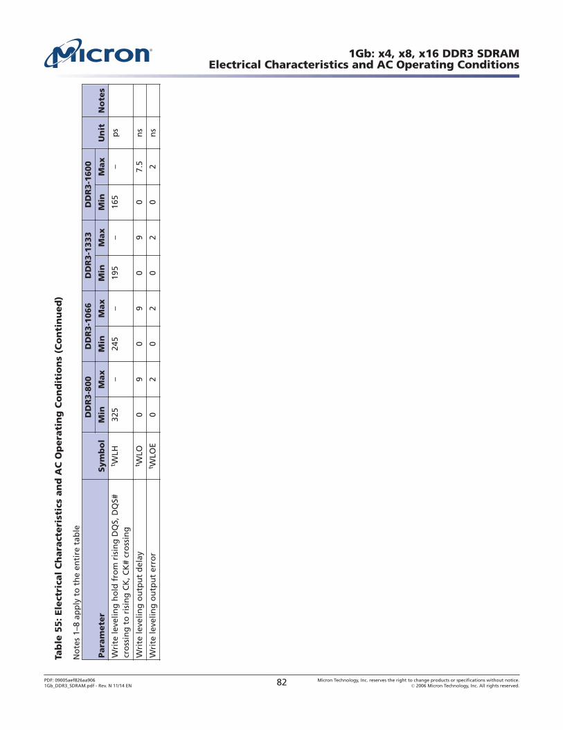
Tab
le 5
5: Ele
ctri
cal
Ch
ara
cteri
stic
s an
d A
C O
pera
tin
g C
on
dit
ion
s (C
on
tin
ued
)
No
tes
1–8
app
ly t
o t
he
enti
re t
able
Para
mete
rSym
bo
l
DD
R3-8
00
DD
R3-1
066
DD
R3-1
333
DD
R3-1
600
Un
itN
ote
sM
inM
ax
Min
Max
Min
Max
Min
Max
Wri
te le
velin
g h
old
fro
m r
isin
g D
QS,
DQ
S#cr
oss
ing
to
ris
ing
CK
, CK
# cr
oss
ing
t WLH
325
–24
5–
195
–16
5–
ps
Wri
te le
velin
g o
utp
ut
del
ayt W
LO0
90
90
90
7.5
ns
Wri
te le
velin
g o
utp
ut
erro
rt W
LOE
02
02
02
02
ns
1Gb: x4, x8, x16 DDR3 SDRAMElectrical Characteristics and AC Operating Conditions
PDF: 09005aef826aa9061Gb_DDR3_SDRAM.pdf - Rev. N 11/14 EN 82 Micron Technology, Inc. reserves the right to change products or specifications without notice.
© 2006 Micron Technology, Inc. All rights reserved.
Notes: 1. AC timing parameters are valid from specified TC MIN to TC MAX values.2. All voltages are referenced to VSS.3. Output timings are only valid for RON34 output buffer selection.4. The unit tCK (AVG) represents the actual tCK (AVG) of the input clock under operation.
The unit CK represents one clock cycle of the input clock, counting the actual clockedges.
5. AC timing and IDD tests may use a VIL-to-VIH swing of up to 900mV in the test environ-ment, but input timing is still referenced to VREF (except tIS, tIH, tDS, and tDH use theAC/DC trip points and CK, CK# and DQS, DQS# use their crossing points). The minimumslew rate for the input signals used to test the device is 1 V/ns for single-ended inputsand 2 V/ns for differential inputs in the range between VIL(AC) and VIH(AC).
6. All timings that use time-based values (ns, μs, ms) should use tCK (AVG) to determine thecorrect number of clocks (Table 55 (page 76) uses CK or tCK [AVG] interchangeably). Inthe case of noninteger results, all minimum limits are to be rounded up to the nearestwhole integer, and all maximum limits are to be rounded down to the nearest wholeinteger.
7. Strobe or DQSdiff refers to the DQS and DQS# differential crossing point when DQS isthe rising edge. Clock or CK refers to the CK and CK# differential crossing point whenCK is the rising edge.
8. This output load is used for all AC timing (except ODT reference timing) and slew rates.The actual test load may be different. The output signal voltage reference point isVDDQ/2 for single-ended signals and the crossing point for differential signals (see Fig-ure 29 (page 68)).
9. When operating in DLL disable mode, Micron does not warrant compliance with normalmode timings or functionality.
10. The clock’s tCK (AVG) is the average clock over any 200 consecutive clocks and tCK (AVG)MIN is the smallest clock rate allowed, with the exception of a deviation due to clockjitter. Input clock jitter is allowed provided it does not exceed values specified and mustbe of a random Gaussian distribution in nature.
11. Spread spectrum is not included in the jitter specification values. However, the inputclock can accommodate spread-spectrum at a sweep rate in the range of 20–60 kHz withan additional 1% of tCK (AVG) as a long-term jitter component; however, the spreadspectrum may not use a clock rate below tCK (AVG) MIN.
12. The clock’s tCH (AVG) and tCL (AVG) are the average half clock period over any 200 con-secutive clocks and is the smallest clock half period allowed, with the exception of a de-viation due to clock jitter. Input clock jitter is allowed provided it does not exceed valuesspecified and must be of a random Gaussian distribution in nature.
13. The period jitter (tJITper) is the maximum deviation in the clock period from the averageor nominal clock. It is allowed in either the positive or negative direction.
14. tCH (ABS) is the absolute instantaneous clock high pulse width as measured from onerising edge to the following falling edge.
15. tCL (ABS) is the absolute instantaneous clock low pulse width as measured from one fall-ing edge to the following rising edge.
16. The cycle-to-cycle jitter tJITcc is the amount the clock period can deviate from one cycleto the next. It is important to keep cycle-to-cycle jitter at a minimum during the DLLlocking time.
17. The cumulative jitter error tERRnper, where n is the number of clocks between 2 and 50,is the amount of clock time allowed to accumulate consecutively away from the averageclock over n number of clock cycles.
18. tDS (base) and tDH (base) values are for a single-ended 1 V/ns slew rate DQs and 2 V/nsslew rate differential DQS, DQS#.
19. These parameters are measured from a data signal (DM, DQ0, DQ1, and so forth) transi-tion edge to its respective data strobe signal (DQS, DQS#) crossing.
1Gb: x4, x8, x16 DDR3 SDRAMElectrical Characteristics and AC Operating Conditions
PDF: 09005aef826aa9061Gb_DDR3_SDRAM.pdf - Rev. N 11/14 EN 83 Micron Technology, Inc. reserves the right to change products or specifications without notice.
© 2006 Micron Technology, Inc. All rights reserved.
20. The setup and hold times are listed converting the base specification values (to whichderating tables apply) to VREF when the slew rate is 1 V/ns. These values, with a slew rateof 1 V/ns, are for reference only.
21. When the device is operated with input clock jitter, this parameter needs to be deratedby the actual tJITper (larger of tJITper (MIN) or tJITper (MAX) of the input clock (outputderatings are relative to the SDRAM input clock).
22. Single-ended signal parameter.23. The DRAM output timing is aligned to the nominal or average clock. Most output pa-
rameters must be derated by the actual jitter error when input clock jitter is present,even when within specification. This results in each parameter becoming larger. The fol-lowing parameters are required to be derated by subtracting tERR10per (MAX): tDQSCK(MIN), tLZDQS (MIN), tLZDQ (MIN), and tAON (MIN). The following parameters are re-quired to be derated by subtracting tERR10per (MIN): tDQSCK (MAX), tHZ (MAX), tLZDQS(MAX), tLZDQ MAX, and tAON (MAX). The parameter tRPRE (MIN) is derated by subtract-ing tJITper (MAX), while tRPRE (MAX) is derated by subtracting tJITper (MIN).
24. The maximum preamble is bound by tLZDQS (MAX).25. These parameters are measured from a data strobe signal (DQS, DQS#) crossing to its re-
spective clock signal (CK, CK#) crossing. The specification values are not affected by theamount of clock jitter applied, as these are relative to the clock signal crossing. Theseparameters should be met whether clock jitter is present.
26. The tDQSCK (DLL_DIS) parameter begins CL + AL - 1 cycles after the READ command.27. The maximum postamble is bound by tHZDQS (MAX).28. Commands requiring a locked DLL are: READ (and RDAP) and synchronous ODT com-
mands. In addition, after any change of latency tXPDLL, timing must be met.29. tIS (base) and tIH (base) values are for a single-ended 1 V/ns control/command/address
slew rate and 2 V/ns CK, CK# differential slew rate.30. These parameters are measured from a command/address signal transition edge to its
respective clock (CK, CK#) signal crossing. The specification values are not affected bythe amount of clock jitter applied as the setup and hold times are relative to the clocksignal crossing that latches the command/address. These parameters should be metwhether clock jitter is present.
31. For these parameters, the DDR3 SDRAM device supports tnPARAM (nCK) = RU(tPARAM[ns]/tCK[AVG] [ns]), assuming all input clock jitter specifications are satisfied. For exam-ple, the device will support tnRP (nCK) = RU(tRP/tCK[AVG]) if all input clock jitter specifi-cations are met. This means that for DDR3-800 6-6-6, of which tRP = 5ns, the device willsupport tnRP = RU(tRP/tCK[AVG]) = 6 as long as the input clock jitter specifications aremet. That is, the PRECHARGE command at T0 and the ACTIVATE command at T0 + 6 arevalid even if six clocks are less than 15ns due to input clock jitter.
32. During READs and WRITEs with auto precharge, the DDR3 SDRAM will hold off the in-ternal PRECHARGE command until tRAS (MIN) has been satisfied.
33. When operating in DLL disable mode, the greater of 4CK or 15ns is satisfied for tWR.34. The start of the write recovery time is defined as follows:
• For BL8 (fixed by MRS or OTF): Rising clock edge four clock cycles after WL• For BC4 (OTF): Rising clock edge four clock cycles after WL• For BC4 (fixed by MRS): Rising clock edge two clock cycles after WL
35. RESET# should be LOW as soon as power starts to ramp to ensure the outputs are inHigh-Z. Until RESET# is LOW, the outputs are at risk of driving and could result in exces-sive current, depending on bus activity.
36. The refresh period is 64ms when TC is less than or equal to 85°C. This equates to an aver-age refresh rate of 7.8125μs. However, nine REFRESH commands should be asserted atleast once every 70.3μs. When TC is greater than 85°C, the refresh period is 32ms.
37. Although CKE is allowed to be registered LOW after a REFRESH command when
1Gb: x4, x8, x16 DDR3 SDRAMElectrical Characteristics and AC Operating Conditions
PDF: 09005aef826aa9061Gb_DDR3_SDRAM.pdf - Rev. N 11/14 EN 84 Micron Technology, Inc. reserves the right to change products or specifications without notice.
© 2006 Micron Technology, Inc. All rights reserved.
tREFPDEN (MIN) is satisfied, there are cases where additional time such as tXPDLL (MIN)is required.
38. ODT turn-on time MIN is when the device leaves High-Z and ODT resistance begins toturn on. ODT turn-on time maximum is when the ODT resistance is fully on. The ODTreference load is shown in Figure 21 (page 54). Designs that were created prior to JEDECtightening the maximum limit from 9ns to 8.5ns will be allowed to have a 9ns maxi-mum.
39. Half-clock output parameters must be derated by the actual tERR10per and tJITdty wheninput clock jitter is present. This results in each parameter becoming larger. The parame-ters tADC (MIN) and tAOF (MIN) are each required to be derated by subtracting bothtERR10per (MAX) and tJITdty (MAX). The parameters tADC (MAX) and tAOF (MAX) arerequired to be derated by subtracting both tERR10per (MAX) and tJITdty (MAX).
40. ODT turn-off time minimum is when the device starts to turn off ODT resistance. ODTturn-off time maximum is when the DRAM buffer is in High-Z. The ODT reference load isshown in Figure 22 (page 57). This output load is used for ODT timings (see Figure 29(page 68)).
41. Pulse width of a input signal is defined as the width between the first crossing ofVREF(DC) and the consecutive crossing of VREF(DC).
42. Should the clock rate be larger than tRFC (MIN), an AUTO REFRESH command shouldhave at least one NOP command between it and another AUTO REFRESH command. Ad-ditionally, if the clock rate is slower than 40ns (25 MHz), all REFRESH commands shouldbe followed by a PRECHARGE ALL command.
43. DRAM devices should be evenly addressed when being accessed. Disproportionate ac-cesses to a particular row address may result in a reduction of REFRESH characteristics orproduct lifetime.
44. When two VIH(AC) values (and two corresponding VIL(AC) values) are listed for a specificspeed bin, the user may choose either value for the input AC level. Whichever value isused, the associated setup time for that AC level must also be used. Additionally, oneVIH(AC) value may be used for address/command inputs and the other VIH(AC) value maybe used for data inputs.
For example, for DDR3-800, two input AC levels are defined: VIH(AC175),min andVIH(AC150),min (corresponding VIL(AC175),min and VIL(AC150),min). For DDR3-800, the address/command inputs must use either VIH(AC175),min with tIS(AC175) of 200ps or VIH(AC150),minwith tIS(AC150) of 350ps; independently, the data inputs must use either VIH(AC175),minwith tDS(AC175) of 75ps or VIH(AC150),min with tDS(AC150) of 125ps.
1Gb: x4, x8, x16 DDR3 SDRAMElectrical Characteristics and AC Operating Conditions
PDF: 09005aef826aa9061Gb_DDR3_SDRAM.pdf - Rev. N 11/14 EN 85 Micron Technology, Inc. reserves the right to change products or specifications without notice.
© 2006 Micron Technology, Inc. All rights reserved.
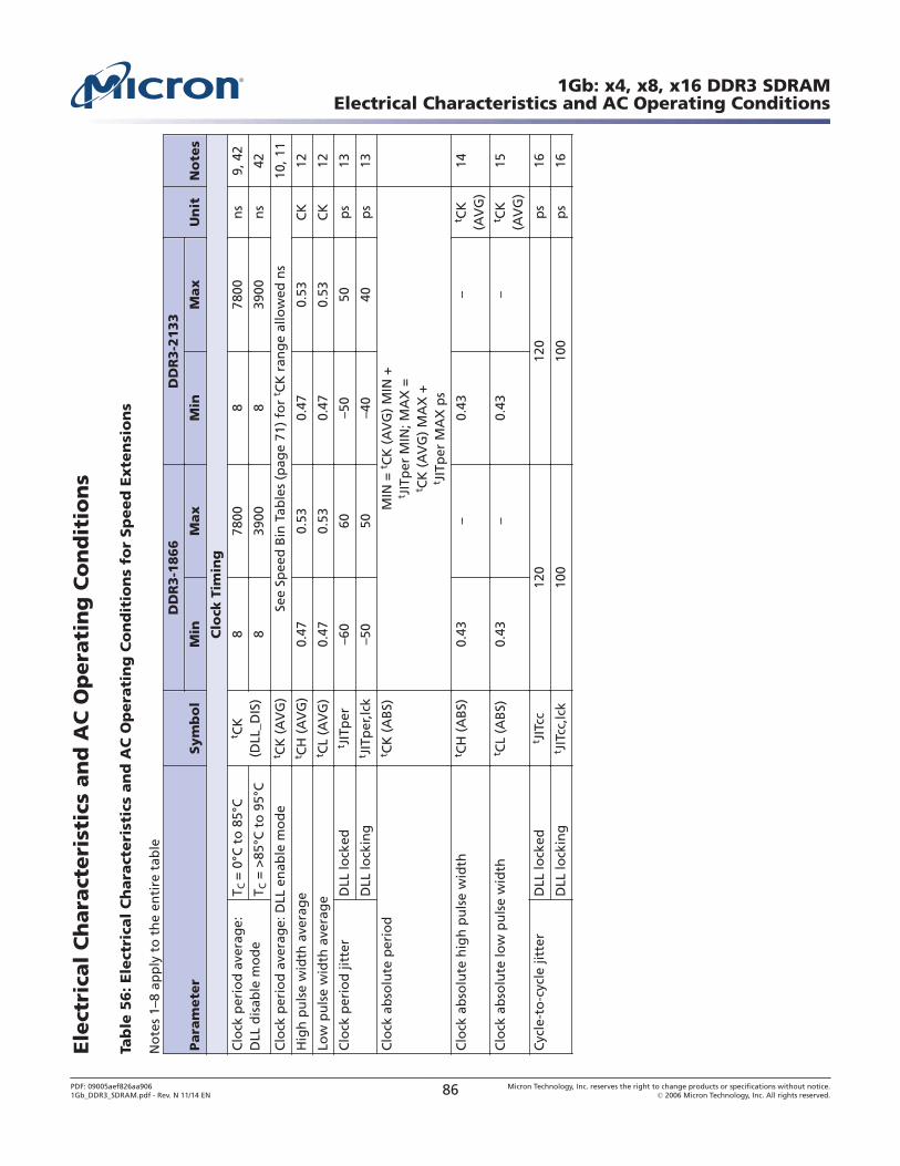
Ele
ctri
cal
Ch
ara
cteri
stic
s an
d A
C O
pera
tin
g C
on
dit
ion
s
Tab
le 5
6: Ele
ctri
cal
Ch
ara
cteri
stic
s an
d A
C O
pera
tin
g C
on
dit
ion
s fo
r Sp
eed
Exte
nsi
on
s
No
tes
1–8
app
ly t
o t
he
enti
re t
able
Para
mete
rSym
bo
l
DD
R3-1
866
DD
R3-2
133
Un
itN
ote
sM
inM
ax
Min
Max
Clo
ck T
imin
g
Clo
ck p
erio
d a
vera
ge:
DLL
dis
able
mo
de
T C =
0°C
to
85°
Ct C
K(D
LL_D
IS)
878
008
7800
ns
9, 4
2
T C =
>85
°C t
o 9
5°C
839
008
3900
ns
42
Clo
ck p
erio
d a
vera
ge:
DLL
en
able
mo
de
t CK
(A
VG
)Se
e Sp
eed
Bin
Tab
les
(pag
e 71
) fo
r t C
K r
ang
e al
low
ed n
s10
, 11
Hig
h p
uls
e w
idth
ave
rag
et C
H (
AV
G)
0.47
0.53
0.47
0.53
CK
12
Low
pu
lse
wid
th a
vera
ge
t CL
(AV
G)
0.47
0.53
0.47
0.53
CK
12
Clo
ck p
erio
d ji
tter
DLL
lock
edt J
ITp
er–6
060
–50
50p
s13
DLL
lock
ing
t JIT
per
,lck
–50
50–4
040
ps
13
Clo
ck a
bso
lute
per
iod
t CK
(A
BS)
MIN
= t C
K (
AV
G)
MIN
+t J
ITp
er M
IN; M
AX
=t C
K (
AV
G)
MA
X +
t JIT
per
MA
X p
s
Clo
ck a
bso
lute
hig
h p
uls
e w
idth
t CH
(A
BS)
0.43
–0.
43–
t CK
(AV
G)
14
Clo
ck a
bso
lute
low
pu
lse
wid
tht C
L (A
BS)
0.43
–0.
43–
t CK
(AV
G)
15
Cyc
le-t
o-c
ycle
jitt
erD
LL lo
cked
t JIT
cc12
012
0p
s16
DLL
lock
ing
t JIT
cc,lc
k10
010
0p
s16
1Gb: x4, x8, x16 DDR3 SDRAMElectrical Characteristics and AC Operating Conditions
PDF: 09005aef826aa9061Gb_DDR3_SDRAM.pdf - Rev. N 11/14 EN 86 Micron Technology, Inc. reserves the right to change products or specifications without notice.
© 2006 Micron Technology, Inc. All rights reserved.
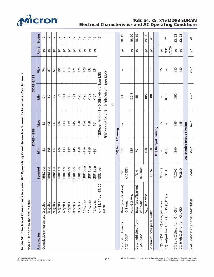
Tab
le 5
6: Ele
ctri
cal
Ch
ara
cteri
stic
s an
d A
C O
pera
tin
g C
on
dit
ion
s fo
r Sp
eed
Exte
nsi
on
s (C
on
tin
ued
)
No
tes
1–8
app
ly t
o t
he
enti
re t
able
Para
mete
rSym
bo
l
DD
R3-1
866
DD
R3-2
133
Un
itN
ote
sM
inM
ax
Min
Max
Cu
mu
lati
ve e
rro
r ac
ross
2 cy
cles
t ER
R2p
er–8
888
-74
74p
s17
3 cy
cles
t ER
R3p
er–1
0510
5-8
787
ps
17
4 cy
cles
t ER
R4p
er–1
1711
7-9
797
ps
17
5 cy
cles
t ER
R5p
er–1
2612
6-1
0510
5p
s17
6 cy
cles
t ER
R6p
er–1
3313
3-1
1111
1p
s17
7 cy
cles
t ER
R7p
er–1
3913
9-1
1611
6p
s17
8 cy
cles
t ER
R8p
er–1
4514
5-1
2112
1p
s17
9 cy
cles
t ER
R9p
er–1
5015
0-1
2512
5p
s17
10 c
ycle
st E
RR
10p
er–1
5415
4-1
2812
8p
s17
11 c
ycle
st E
RR
11p
er–1
5815
8-1
3213
2p
s17
12 c
ycle
st E
RR
12p
er–1
6116
1-1
3413
4p
s17
n =
13,
14
. . .
49, 5
0cy
cles
t ER
Rn
per
t ER
Rn
per
MIN
= (
1 +
0.6
8ln
[n])
× t J
ITp
er M
IN
t ER
Rn
per
MA
X =
(1
+ 0
.68l
n[n
]) ×
t JIT
per
MA
X
ps
17
DQ
In
pu
t Ti
min
g
Dat
a se
tup
tim
e to
DQ
S, D
QS#
Bas
e (s
pec
ific
atio
n)
@ 2
V/n
s
t DS
(AC
135)
68–
53–
ps
18, 1
9
VR
EF @
2 V
/ns
135
–12
0.5
–p
s19
, 20
Dat
a h
old
tim
e fr
om
DQ
S, D
QS#
Bas
e (s
pec
ific
atio
n)
@ 2
V/n
s
t DH
(DC
100)
70–
55–
ps
18, 1
9
VR
EF @
2 V
/ns
120
–10
5–
ps
19, 2
0
Min
imu
m d
ata
pu
lse
wid
tht D
IPW
320
–28
0–
ps
41
DQ
Ou
tpu
t Ti
min
g
DQ
S, D
QS#
to
DQ
ske
w, p
er a
cces
st D
QSQ
–85
–75
ps
DQ
ou
tpu
t h
old
tim
e fr
om
DQ
S, D
QS#
t QH
0.38
–0.
38–
t CK
(AV
G)
21
DQ
Lo
w-Z
tim
e fr
om
CK
, CK
#t L
ZDQ
–390
195
–360
180
ps
22, 2
3
DQ
Hig
h-Z
tim
e fr
om
CK
, CK
#t H
ZDQ
–19
5–
180
ps
22, 2
3
DQ
Str
ob
e I
np
ut
Tim
ing
DQ
S, D
QS#
ris
ing
to
CK
, CK
# ri
sin
gt D
QSS
–0.2
70.
27–0
.27
0.27
CK
25
1Gb: x4, x8, x16 DDR3 SDRAMElectrical Characteristics and AC Operating Conditions
PDF: 09005aef826aa9061Gb_DDR3_SDRAM.pdf - Rev. N 11/14 EN 87 Micron Technology, Inc. reserves the right to change products or specifications without notice.
© 2006 Micron Technology, Inc. All rights reserved.
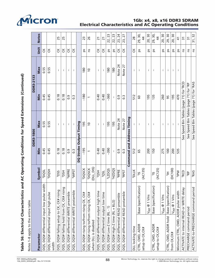
Tab
le 5
6: Ele
ctri
cal
Ch
ara
cteri
stic
s an
d A
C O
pera
tin
g C
on
dit
ion
s fo
r Sp
eed
Exte
nsi
on
s (C
on
tin
ued
)
No
tes
1–8
app
ly t
o t
he
enti
re t
able
Para
mete
rSym
bo
l
DD
R3-1
866
DD
R3-2
133
Un
itN
ote
sM
inM
ax
Min
Max
DQ
S, D
QS#
dif
fere
nti
al in
pu
t lo
w p
uls
e w
idth
t DQ
SL0.
450.
550.
450.
55C
K
DQ
S, D
QS#
dif
fere
nti
al in
pu
t h
igh
pu
lse
wid
th
t DQ
SH0.
450.
550.
450.
55C
K
DQ
S, D
QS#
fal
ling
set
up
to
CK
, CK
# ri
sin
gt D
SS0.
18–
0.18
–C
K25
DQ
S, D
QS#
fal
ling
ho
ld f
rom
CK
, CK
# ri
sin
gt D
SH0.
18–
0.18
–C
K25
DQ
S, D
QS#
dif
fere
nti
al W
RIT
E p
ream
ble
t WPR
E0.
9–
0.9
–C
K
DQ
S, D
QS#
dif
fere
nti
al W
RIT
E p
ost
amb
let W
PST
0.3
–0.
3–
CK
DQ
Str
ob
e O
utp
ut
Tim
ing
DQ
S, D
QS#
ris
ing
to
/fro
m r
isin
g C
K, C
K#
t DQ
SCK
–195
195
–180
180
ps
23
DQ
S, D
QS#
ris
ing
to
/fro
m r
isin
g C
K, C
K#
wh
en D
LL is
dis
able
d
t DQ
SCK
(DLL
_DIS
)1
101
10n
s26
DQ
S, D
QS#
dif
fere
nti
al o
utp
ut
hig
h t
ime
t QSH
0.40
–0.
40–
CK
21
DQ
S, D
QS#
dif
fere
nti
al o
utp
ut
low
tim
et Q
SL0.
40–
0.40
–C
K21
DQ
S, D
QS#
Lo
w-Z
tim
e (R
L -
1)t L
ZDQ
S–3
9019
5–3
6018
0p
s22
, 23
DQ
S, D
QS#
Hig
h-Z
tim
e (R
L +
BL/
2)t H
ZDQ
S–
195
–18
0p
s22
, 23
DQ
S, D
QS#
dif
fere
nti
al R
EAD
pre
amb
let R
PRE
0.9
No
te 2
40.
9N
ote
24
CK
23, 2
4
DQ
S, D
QS#
dif
fere
nti
al R
EAD
po
stam
ble
t RPS
T0.
3N
ote
27
0.3
No
te 2
7C
K23
, 27
Co
mm
an
d a
nd
Ad
dre
ss T
imin
g
DLL
lock
ing
tim
et D
LLK
512
–51
2–
CK
28
CTR
L, C
MD
, AD
DR
setu
p t
o C
K,C
K#
Bas
e (s
pec
ific
atio
n)
t IS(A
C13
5)65
–60
–p
s29
, 30,
44
VR
EF @
1 V
/ns
200
–19
5–
ps
20, 3
0
CTR
L, C
MD
, AD
DR
setu
p t
o C
K,C
K#
Bas
e (s
pec
ific
atio
n)
t IS(A
C12
5)15
0–
135
–p
s29
, 30,
44
VR
EF @
1 V
/ns
275
–26
0–
ps
20, 3
0
CTR
L, C
MD
, AD
DR
ho
ldfr
om
CK
,CK
#B
ase
(sp
ecif
icat
ion
)t IH
(DC
100)
100
–95
–p
s29
, 30
VR
EF @
1 V
/ns
200
–19
5–
ps
20, 3
0
Min
imu
m C
TRL,
CM
D, A
DD
R p
uls
e w
idth
t IPW
535
–47
0–
ps
41
AC
TIV
ATE
to
inte
rnal
REA
D o
r W
RIT
E d
elay
t RC
DSe
e Sp
eed
Bin
Tab
les
(pag
e 71
) fo
r t R
CD
ns
31
PREC
HA
RG
E co
mm
and
per
iod
t RP
See
Spee
d B
in T
able
s (p
age
71)
for
t RP
ns
31
AC
TIV
ATE
-to
-PR
ECH
AR
GE
com
man
d p
erio
dt R
AS
See
Spee
d B
in T
able
s (p
age
71)
for
t RA
Sn
s31
, 32
1Gb: x4, x8, x16 DDR3 SDRAMElectrical Characteristics and AC Operating Conditions
PDF: 09005aef826aa9061Gb_DDR3_SDRAM.pdf - Rev. N 11/14 EN 88 Micron Technology, Inc. reserves the right to change products or specifications without notice.
© 2006 Micron Technology, Inc. All rights reserved.
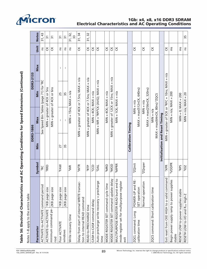
Tab
le 5
6: Ele
ctri
cal
Ch
ara
cteri
stic
s an
d A
C O
pera
tin
g C
on
dit
ion
s fo
r Sp
eed
Exte
nsi
on
s (C
on
tin
ued
)
No
tes
1–8
app
ly t
o t
he
enti
re t
able
Para
mete
rSym
bo
l
DD
R3-1
866
DD
R3-2
133
Un
itN
ote
sM
inM
ax
Min
Max
AC
TIV
ATE
-to
-AC
TIV
ATE
co
mm
and
per
iod
t RC
See
Spee
d B
in T
able
s (p
age
71)
for
t RC
ns
31, 4
3
AC
TIV
ATE
-to
-AC
TIV
ATE
min
imu
m c
om
man
d p
e-ri
od
1KB
pag
e si
zet R
RD
MIN
= g
reat
er o
f 4C
K o
r 5n
sC
K31
2KB
pag
e si
zeM
IN =
gre
ater
of
4CK
or
6ns
CK
31
Fou
r A
CTI
VA
TEw
ind
ow
s1K
B p
age
size
t FA
W27
–25
–n
s31
2KB
pag
e si
ze35
–35
–n
s31
Wri
te r
eco
very
tim
et W
RM
IN =
15n
s; M
AX
= n
/an
s31
, 32,
33
Del
ay f
rom
sta
rt o
f in
tern
al W
RIT
E tr
ansa
c-ti
on
to
inte
rnal
REA
D c
om
man
d
t WTR
MIN
= g
reat
er o
f 4C
K o
r 7.
5ns;
MA
X =
n/a
CK
31, 3
4
REA
D-t
o-P
REC
HA
RG
E ti
me
t RTP
MIN
= g
reat
er o
f 4C
K o
r 7.
5ns;
MA
X =
n/a
CK
31, 3
2
CA
S#-t
o-C
AS#
co
mm
and
del
ayt C
CD
MIN
= 4
CK
; MA
X =
n/a
CK
Au
to p
rech
arg
e w
rite
rec
ove
ry +
pre
char
ge
tim
e
t DA
LM
IN =
WR
+ t R
P/t C
K (
AV
G);
MA
X =
n/a
CK
MO
DE
REG
ISTE
R S
ET c
om
man
d c
ycle
tim
et M
RD
MIN
= 4
CK
; MA
X =
n/a
CK
MO
DE
REG
ISTE
R S
ET c
om
man
d u
pd
ate
del
ayt M
OD
MIN
= g
reat
er o
f 12
CK
or
15n
s; M
AX
= n
/aC
K
MU
LTIP
UR
POSE
REG
ISTE
R R
EAD
bu
rst
end
to
mo
de
reg
iste
r se
t fo
r m
ult
ipu
rpo
se r
egis
ter
exit
t MPR
RM
IN =
1C
K; M
AX
= n
/aC
K
Cali
bra
tio
n T
imin
g
ZQC
L co
mm
and
: Lo
ng
calib
rati
on
tim
ePO
WER
-UP
and
RE-
SET
op
erat
ion
t ZQ
init
MIN
= n
/aM
AX
= m
ax(5
12n
CK
, 640
ns)
CK
No
rmal
op
erat
ion
t ZQ
op
erM
IN =
n/a
MA
X =
max
(256
nC
K, 3
20n
s)C
K
ZQC
S co
mm
and
: Sh
ort
cal
ibra
tio
n t
ime
MIN
= n
/aM
AX
= m
ax(6
4nC
K, 8
0ns)
t ZQ
CS
CK
Init
iali
zati
on
an
d R
ese
t Ti
min
g
Exit
res
et f
rom
CK
E H
IGH
to
a v
alid
co
mm
and
t XPR
MIN
= g
reat
er o
f 5C
K o
r t R
FC +
10n
s; M
AX
= n
/aC
K
Beg
in p
ow
er s
up
ply
ram
p t
o p
ow
er s
up
plie
sst
able
t VD
DPR
MIN
= n
/a; M
AX
= 2
00m
s
RES
ET#
LOW
to
po
wer
su
pp
lies
stab
let R
PSM
IN =
0; M
AX
= 2
00m
s
RES
ET#
LOW
to
I/O
an
d R
TT H
igh
-Zt IO
ZM
IN =
n/a
; MA
X =
20
ns
35
1Gb: x4, x8, x16 DDR3 SDRAMElectrical Characteristics and AC Operating Conditions
PDF: 09005aef826aa9061Gb_DDR3_SDRAM.pdf - Rev. N 11/14 EN 89 Micron Technology, Inc. reserves the right to change products or specifications without notice.
© 2006 Micron Technology, Inc. All rights reserved.
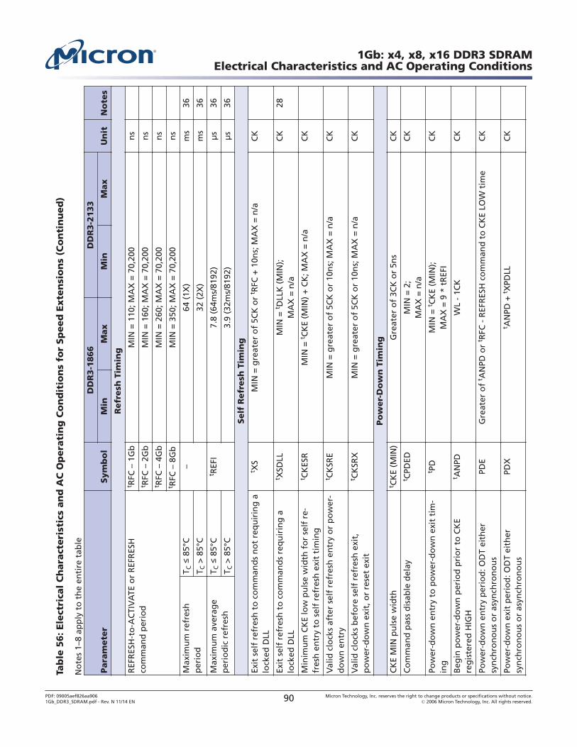
Tab
le 5
6: Ele
ctri
cal
Ch
ara
cteri
stic
s an
d A
C O
pera
tin
g C
on
dit
ion
s fo
r Sp
eed
Exte
nsi
on
s (C
on
tin
ued
)
No
tes
1–8
app
ly t
o t
he
enti
re t
able
Para
mete
rSym
bo
l
DD
R3-1
866
DD
R3-2
133
Un
itN
ote
sM
inM
ax
Min
Max
Refr
esh
Tim
ing
REF
RES
H-t
o-A
CTI
VA
TE o
r R
EFR
ESH
com
man
d p
erio
d
t RFC
– 1
Gb
MIN
= 1
10; M
AX
= 7
0,20
0n
s
t RFC
– 2
Gb
MIN
= 1
60; M
AX
= 7
0,20
0n
s
t RFC
– 4
Gb
MIN
= 2
60; M
AX
= 7
0,20
0n
s
t RFC
– 8
Gb
MIN
= 3
50; M
AX
= 7
0,20
0n
s
Max
imu
m r
efre
shp
erio
dT C
≤ 8
5°C
–64
(1X
)m
s36
T C >
85°
C32
(2X
)m
s36
Max
imu
m a
vera
ge
per
iod
ic r
efre
shT C
≤ 8
5°C
t REF
I7.
8 (6
4ms/
8192
)μ
s36
T C >
85°
C3.
9 (3
2ms/
8192
)μ
s36
Self
Refr
esh
Tim
ing
Exit
sel
f re
fres
h t
o c
om
man
ds
no
t re
qu
irin
g a
lock
ed D
LL
t XS
MIN
= g
reat
er o
f 5C
K o
r t R
FC +
10n
s; M
AX
= n
/aC
K
Exit
sel
f re
fres
h t
o c
om
man
ds
req
uir
ing
alo
cked
DLL
t XSD
LLM
IN =
t DLL
K (
MIN
);M
AX
= n
/aC
K28
Min
imu
m C
KE
low
pu
lse
wid
th f
or
self
re-
fres
h e
ntr
y to
sel
f re
fres
h e
xit
tim
ing
t CK
ESR
MIN
= t C
KE
(MIN
) +
CK
; MA
X =
n/a
CK
Val
id c
lock
s af
ter
self
ref
resh
en
try
or
po
wer
-d
ow
n e
ntr
y
t CK
SRE
MIN
= g
reat
er o
f 5C
K o
r 10
ns;
MA
X =
n/a
CK
Val
id c
lock
s b
efo
re s
elf
refr
esh
exi
t,p
ow
er-d
ow
n e
xit,
or
rese
t ex
it
t CK
SRX
MIN
= g
reat
er o
f 5C
K o
r 10
ns;
MA
X =
n/a
CK
Po
wer-
Do
wn
Tim
ing
CK
E M
IN p
uls
e w
idth
t CK
E (M
IN)
Gre
ater
of
3CK
or
5ns
CK
Co
mm
and
pas
s d
isab
le d
elay
t CPD
EDM
IN =
2;
MA
X =
n/a
CK
Pow
er-d
ow
n e
ntr
y to
po
wer
-do
wn
exi
t ti
m-
ing
t PD
MIN
= t C
KE
(MIN
);M
AX
= 9
* t
REF
IC
K
Beg
in p
ow
er-d
ow
n p
erio
d p
rio
r to
CK
Ere
gis
tere
d H
IGH
t AN
PDW
L -
1CK
CK
Pow
er-d
ow
n e
ntr
y p
erio
d: O
DT
eith
ersy
nch
ron
ou
s o
r as
ynch
ron
ou
sPD
EG
reat
er o
f t A
NPD
or
t RFC
- R
EFR
ESH
co
mm
and
to
CK
E LO
W t
ime
CK
Pow
er-d
ow
n e
xit
per
iod
: OD
T ei
ther
syn
chro
no
us
or
asyn
chro
no
us
PDX
t AN
PD +
t XPD
LLC
K
1Gb: x4, x8, x16 DDR3 SDRAMElectrical Characteristics and AC Operating Conditions
PDF: 09005aef826aa9061Gb_DDR3_SDRAM.pdf - Rev. N 11/14 EN 90 Micron Technology, Inc. reserves the right to change products or specifications without notice.
© 2006 Micron Technology, Inc. All rights reserved.
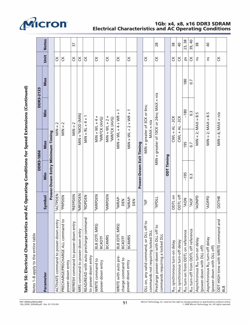
Tab
le 5
6: Ele
ctri
cal
Ch
ara
cteri
stic
s an
d A
C O
pera
tin
g C
on
dit
ion
s fo
r Sp
eed
Exte
nsi
on
s (C
on
tin
ued
)
No
tes
1–8
app
ly t
o t
he
enti
re t
able
Para
mete
rSym
bo
l
DD
R3-1
866
DD
R3-2
133
Un
itN
ote
sM
inM
ax
Min
Max
Po
wer-
Do
wn
En
try M
inim
um
Tim
ing
AC
TIV
ATE
co
mm
and
to
po
wer
-do
wn
en
try
t AC
TPD
ENM
IN =
2C
K
PREC
HA
RG
E/PR
ECH
AR
GE
ALL
co
mm
and
to
po
wer
-do
wn
en
try
t PR
PDEN
MIN
= 2
CK
REF
RES
H c
om
man
d t
o p
ow
er-d
ow
n e
ntr
yt R
EFPD
ENM
IN =
2C
K37
MR
S co
mm
and
to
po
wer
-do
wn
en
try
t MR
SPD
ENM
IN =
t MO
D (
MIN
)C
K
REA
D/R
EAD
wit
h a
uto
pre
char
ge
com
man
dto
po
wer
-do
wn
en
try
t RD
PDEN
MIN
= R
L +
4 +
1C
K
WR
ITE
com
man
d t
op
ow
er-d
ow
n e
ntr
yB
L8 (
OTF
, MR
S)B
C4O
TF
t WR
PDEN
MIN
= W
L +
4 +
t WR
/t CK
(A
VG
)C
K
BC
4MR
St W
RPD
ENM
IN =
WL
+ 2
+t W
R/t C
K (
AV
G)
CK
WR
ITE
wit
h a
uto
pre
-ch
arg
e co
mm
and
to
po
wer
-do
wn
en
try
BL8
(O
TF, M
RS)
BC
4OTF
t WR
AP-
DEN
MIN
= W
L +
4 +
WR
+ 1
CK
BC
4MR
St W
RA
P-D
ENM
IN =
WL
+ 2
+ W
R +
1C
K
Po
wer-
Do
wn
Exit
Tim
ing
DLL
on
, an
y va
lid c
om
man
d, o
r D
LL o
ff t
oco
mm
and
s n
ot
req
uir
ing
lock
ed D
LL
t XP
MIN
= g
reat
er o
f 3C
K o
r 6n
s;M
AX
= n
/aC
K
Prec
har
ge
po
wer
-do
wn
wit
h D
LL o
ff t
oco
mm
and
s re
qu
irin
g a
lock
ed D
LL
t XPD
LLM
IN =
gre
ater
of
10C
K o
r 24
ns;
MA
X =
n/a
CK
28
OD
T Ti
min
g
RTT
syn
chro
no
us
turn
-on
del
ayO
DTL
on
CW
L +
AL
- 2C
KC
K38
RTT
syn
chro
no
us
turn
-off
del
ayO
DTL
off
CW
L +
AL
- 2C
KC
K40
RTT
tu
rn-o
n f
rom
OD
TL o
n r
efer
ence
t AO
N–1
9519
5–1
8018
0p
s23
, 38
RTT
tu
rn-o
ff f
rom
OD
TL o
ff r
efer
ence
t AO
F0.
30.
70.
30.
7C
K39
, 40
Asy
nch
ron
ou
s R
TT t
urn
-on
del
ay(p
ow
er-d
ow
n w
ith
DLL
off
)
t AO
NPD
MIN
= 2
; MA
X =
8.5
ns
38
Asy
nch
ron
ou
s R
TT t
urn
-off
del
ay(p
ow
er-d
ow
n w
ith
DLL
off
)
t AO
FPD
MIN
= 2
; MA
X =
8.5
ns
40
OD
T H
IGH
tim
e w
ith
WR
ITE
com
man
d a
nd
BL8
OD
TH8
MIN
= 6
; MA
X =
n/a
CK
1Gb: x4, x8, x16 DDR3 SDRAMElectrical Characteristics and AC Operating Conditions
PDF: 09005aef826aa9061Gb_DDR3_SDRAM.pdf - Rev. N 11/14 EN 91 Micron Technology, Inc. reserves the right to change products or specifications without notice.
© 2006 Micron Technology, Inc. All rights reserved.
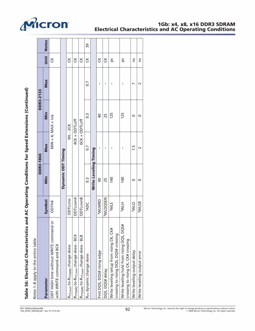
Tab
le 5
6: Ele
ctri
cal
Ch
ara
cteri
stic
s an
d A
C O
pera
tin
g C
on
dit
ion
s fo
r Sp
eed
Exte
nsi
on
s (C
on
tin
ued
)
No
tes
1–8
app
ly t
o t
he
enti
re t
able
Para
mete
rSym
bo
l
DD
R3-1
866
DD
R3-2
133
Un
itN
ote
sM
inM
ax
Min
Max
OD
T H
IGH
tim
e w
ith
ou
t W
RIT
E co
mm
and
or
wit
h W
RIT
E co
mm
and
an
d B
C4
OD
TH4
MIN
= 4
; MA
X =
n/a
CK
Dyn
am
ic O
DT
Tim
ing
RTT
,no
m-t
o-R
TT(W
R) c
han
ge
skew
OD
TLcn
wW
L -
2CK
CK
RTT
(WR
)-to
-RTT
,no
m c
han
ge
skew
- B
C4
OD
TLcw
n4
4CK
+ O
DTL
off
CK
RTT
(WR
)-to
-RTT
,no
m c
han
ge
skew
- B
L8O
DTL
cwn
86C
K +
OD
TLo
ffC
K
RTT
dyn
amic
ch
ang
e sk
ewt A
DC
0.3
0.7
0.3
0.7
CK
39
Wri
te L
eveli
ng
Tim
ing
Firs
t D
QS,
DQ
S# r
isin
g e
dg
et W
LMR
D40
–40
–C
K
DQ
S, D
QS#
del
ayt W
LDQ
SEN
25–
25–
CK
Wri
te le
velin
g s
etu
p f
rom
ris
ing
CK
, CK
#cr
oss
ing
to
ris
ing
DQ
S, D
QS#
cro
ssin
g
t WLS
140
–12
5–
ps
Wri
te le
velin
g h
old
fro
m r
isin
g D
QS,
DQ
S#cr
oss
ing
to
ris
ing
CK
, CK
# cr
oss
ing
t WLH
140
–12
5–
ps
Wri
te le
velin
g o
utp
ut
del
ayt W
LO0
7.5
07
ns
Wri
te le
velin
g o
utp
ut
erro
rt W
LOE
02
02
ns
1Gb: x4, x8, x16 DDR3 SDRAMElectrical Characteristics and AC Operating Conditions
PDF: 09005aef826aa9061Gb_DDR3_SDRAM.pdf - Rev. N 11/14 EN 92 Micron Technology, Inc. reserves the right to change products or specifications without notice.
© 2006 Micron Technology, Inc. All rights reserved.
Notes: 1. AC timing parameters are valid from specified TC MIN to TC MAX values.2. All voltages are referenced to VSS.3. Output timings are only valid for RON34 output buffer selection.4. The unit tCK (AVG) represents the actual tCK (AVG) of the input clock under operation.
The unit CK represents one clock cycle of the input clock, counting the actual clockedges.
5. AC timing and IDD tests may use a VIL-to-VIH swing of up to 900mV in the test environ-ment, but input timing is still referenced to VREF (except tIS, tIH, tDS, and tDH use theAC/DC trip points and CK, CK# and DQS, DQS# use their crossing points). The minimumslew rate for the input signals used to test the device is 1 V/ns for single-ended inputs(DQs are at 2V/ns for DDR3-1866 and DDR3-2133) and 2 V/ns for differential inputs inthe range between VIL(AC) and VIH(AC).
6. All timings that use time-based values (ns, μs, ms) should use tCK (AVG) to determine thecorrect number of clocks (Table 56 (page 86) uses CK or tCK [AVG] interchangeably). Inthe case of noninteger results, all minimum limits are to be rounded up to the nearestwhole integer, and all maximum limits are to be rounded down to the nearest wholeinteger.
7. Strobe or DQSdiff refers to the DQS and DQS# differential crossing point when DQS isthe rising edge. Clock or CK refers to the CK and CK# differential crossing point whenCK is the rising edge.
8. This output load is used for all AC timing (except ODT reference timing) and slew rates.The actual test load may be different. The output signal voltage reference point isVDDQ/2 for single-ended signals and the crossing point for differential signals (see Fig-ure 29 (page 68)).
9. When operating in DLL disable mode, Micron does not warrant compliance with normalmode timings or functionality.
10. The clock’s tCK (AVG) is the average clock over any 200 consecutive clocks and tCK (AVG)MIN is the smallest clock rate allowed, with the exception of a deviation due to clockjitter. Input clock jitter is allowed provided it does not exceed values specified and mustbe of a random Gaussian distribution in nature.
11. Spread spectrum is not included in the jitter specification values. However, the inputclock can accommodate spread-spectrum at a sweep rate in the range of 20–60 kHz withan additional 1% of tCK (AVG) as a long-term jitter component; however, the spreadspectrum may not use a clock rate below tCK (AVG) MIN.
12. The clock’s tCH (AVG) and tCL (AVG) are the average half clock period over any 200 con-secutive clocks and is the smallest clock half period allowed, with the exception of a de-viation due to clock jitter. Input clock jitter is allowed provided it does not exceed valuesspecified and must be of a random Gaussian distribution in nature.
13. The period jitter (tJITper) is the maximum deviation in the clock period from the averageor nominal clock. It is allowed in either the positive or negative direction.
14. tCH (ABS) is the absolute instantaneous clock high pulse width as measured from onerising edge to the following falling edge.
15. tCL (ABS) is the absolute instantaneous clock low pulse width as measured from one fall-ing edge to the following rising edge.
16. The cycle-to-cycle jitter tJITcc is the amount the clock period can deviate from one cycleto the next. It is important to keep cycle-to-cycle jitter at a minimum during the DLLlocking time.
17. The cumulative jitter error tERRnper, where n is the number of clocks between 2 and 50,is the amount of clock time allowed to accumulate consecutively away from the averageclock over n number of clock cycles.
18. tDS (base) and tDH (base) values are for a single-ended 1 V/ns slew rate DQs (DQs are at2V/ns for DDR3-1866 and DDR3-2133) and 2 V/ns slew rate differential DQS, DQS#.
1Gb: x4, x8, x16 DDR3 SDRAMElectrical Characteristics and AC Operating Conditions
PDF: 09005aef826aa9061Gb_DDR3_SDRAM.pdf - Rev. N 11/14 EN 93 Micron Technology, Inc. reserves the right to change products or specifications without notice.
© 2006 Micron Technology, Inc. All rights reserved.
19. These parameters are measured from a data signal (DM, DQ0, DQ1, and so forth) transi-tion edge to its respective data strobe signal (DQS, DQS#) crossing.
20. The setup and hold times are listed converting the base specification values (to whichderating tables apply) to VREF when the slew rate is 1 V/ns (DQs are at 2V/ns forDDR3-1866 and DDR3-2133). These values, with a slew rate of 1 V/ns (DQs are at 2V/nsfor DDR3-1866 and DDR3-2133), are for reference only.
21. When the device is operated with input clock jitter, this parameter needs to be deratedby the actual tJITper (larger of tJITper (MIN) or tJITper (MAX) of the input clock (outputderatings are relative to the SDRAM input clock).
22. Single-ended signal parameter.23. The DRAM output timing is aligned to the nominal or average clock. Most output pa-
rameters must be derated by the actual jitter error when input clock jitter is present,even when within specification. This results in each parameter becoming larger. The fol-lowing parameters are required to be derated by subtracting tERR10per (MAX): tDQSCK(MIN), tLZDQS (MIN), tLZDQ (MIN), and tAON (MIN). The following parameters are re-quired to be derated by subtracting tERR10per (MIN): tDQSCK (MAX), tHZ (MAX), tLZDQS(MAX), tLZDQ (MAX), and tAON (MAX). The parameter tRPRE (MIN) is derated by sub-tracting tJITper (MAX), while tRPRE (MAX) is derated by subtracting tJITper (MIN).
24. The maximum preamble is bound by tLZDQS (MAX).25. These parameters are measured from a data strobe signal (DQS, DQS#) crossing to its re-
spective clock signal (CK, CK#) crossing. The specification values are not affected by theamount of clock jitter applied, as these are relative to the clock signal crossing. Theseparameters should be met whether clock jitter is present.
26. The tDQSCK (DLL_DIS) parameter begins CL + AL - 1 cycles after the READ command.27. The maximum postamble is bound by tHZDQS (MAX).28. Commands requiring a locked DLL are: READ (and RDAP) and synchronous ODT com-
mands. In addition, after any change of latency tXPDLL, timing must be met.29. tIS (base) and tIH (base) values are for a single-ended 1 V/ns control/command/address
slew rate and 2 V/ns CK, CK# differential slew rate.30. These parameters are measured from a command/address signal transition edge to its
respective clock (CK, CK#) signal crossing. The specification values are not affected bythe amount of clock jitter applied as the setup and hold times are relative to the clocksignal crossing that latches the command/address. These parameters should be metwhether clock jitter is present.
31. For these parameters, the DDR3 SDRAM device supports tnPARAM (nCK) = RU(tPARAM[ns]/tCK[AVG] [ns]), assuming all input clock jitter specifications are satisfied. For exam-ple, the device will support tnRP (nCK) = RU(tRP/tCK[AVG]) if all input clock jitter specifi-cations are met. This means that for DDR3-800 6-6-6, of which tRP = 5ns, the device willsupport tnRP = RU(tRP/tCK[AVG]) = 6 as long as the input clock jitter specifications aremet. That is, the PRECHARGE command at T0 and the ACTIVATE command at T0 + 6 arevalid even if six clocks are less than 15ns due to input clock jitter.
32. During READs and WRITEs with auto precharge, the DDR3 SDRAM will hold off the in-ternal PRECHARGE command until tRAS (MIN) has been satisfied.
33. When operating in DLL disable mode, the greater of 5CK or 15ns is satisfied for tWR.34. The start of the write recovery time is defined as follows:
• For BL8 (fixed by MRS or OTF): Rising clock edge four clock cycles after WL• For BC4 (OTF): Rising clock edge four clock cycles after WL• For BC4 (fixed by MRS): Rising clock edge two clock cycles after WL
35. RESET# should be LOW as soon as power starts to ramp to ensure the outputs are inHigh-Z. Until RESET# is LOW, the outputs are at risk of driving and could result in exces-sive current, depending on bus activity.
1Gb: x4, x8, x16 DDR3 SDRAMElectrical Characteristics and AC Operating Conditions
PDF: 09005aef826aa9061Gb_DDR3_SDRAM.pdf - Rev. N 11/14 EN 94 Micron Technology, Inc. reserves the right to change products or specifications without notice.
© 2006 Micron Technology, Inc. All rights reserved.
36. The refresh period is 64ms when TC is less than or equal to 85°C. This equates to an aver-age refresh rate of 7.8125μs. However, nine REFRESH commands should be asserted atleast once every 70.3μs. When TC is greater than 85°C, the refresh period is 32ms.
37. Although CKE is allowed to be registered LOW after a REFRESH command whentREFPDEN (MIN) is satisfied, there are cases where additional time such as tXPDLL (MIN)is required.
38. ODT turn-on time MIN is when the device leaves High-Z and ODT resistance begins toturn on. ODT turn-on time maximum is when the ODT resistance is fully on. The ODTreference load is shown in Figure 21 (page 54). Designs that were created prior to JEDECtightening the maximum limit from 9ns to 8.5ns will be allowed to have a 9ns maxi-mum.
39. Half-clock output parameters must be derated by the actual tERR10per and tJITdty wheninput clock jitter is present. This results in each parameter becoming larger. The parame-ters tADC (MIN) and tAOF (MIN) are each required to be derated by subtracting bothtERR10per (MAX) and tJITdty (MAX). The parameters tADC (MAX) and tAOF (MAX) arerequired to be derated by subtracting both tERR10per (MAX) and tJITdty (MAX).
40. ODT turn-off time minimum is when the device starts to turn off ODT resistance. ODTturn-off time maximum is when the DRAM buffer is in High-Z. The ODT reference load isshown in Figure 22 (page 57). This output load is used for ODT timings (see Figure 29(page 68)).
41. Pulse width of a input signal is defined as the width between the first crossing ofVREF(DC) and the consecutive crossing of VREF(DC).
42. Should the clock rate be larger than tRFC (MIN), an AUTO REFRESH command shouldhave at least one NOP command between it and another AUTO REFRESH command. Ad-ditionally, if the clock rate is slower than 40ns (25 MHz), all REFRESH commands shouldbe followed by a PRECHARGE ALL command.
43. DRAM devices should be evenly addressed when being accessed. Disproportionate ac-cesses to a particular row address may result in a reduction of REFRESH characteristics orproduct lifetime.
44. When two VIH(AC) values (and two corresponding VIL(AC) values) are listed for a specificspeed bin, the user may choose either value for the input AC level. Whichever value isused, the associated setup time for that AC level must also be used. Additionally, oneVIH(AC) value may be used for address/command inputs and the other VIH(AC) value maybe used for data inputs.
For example, for DDR3-800, two input AC levels are defined: VIH(AC175),min andVIH(AC150),min (corresponding VIL(AC175),min and VIL(AC150),min). For DDR3-800, the address/command inputs must use either VIH(AC175),min with tIS(AC175) of 200ps or VIH(AC150),minwith tIS(AC150) of 350ps; independently, the data inputs must use either VIH(AC175),minwith tDS(AC175) of 75ps or VIH(AC150),min with tDS(AC150) of 125ps.
1Gb: x4, x8, x16 DDR3 SDRAMElectrical Characteristics and AC Operating Conditions
PDF: 09005aef826aa9061Gb_DDR3_SDRAM.pdf - Rev. N 11/14 EN 95 Micron Technology, Inc. reserves the right to change products or specifications without notice.
© 2006 Micron Technology, Inc. All rights reserved.
Command and Address Setup, Hold, and DeratingThe total tIS (setup time) and tIH (hold time) required is calculated by adding the datasheet tIS (base) and tIH (base) values (see Table 57; values come from Table 55(page 76)) to the ΔtIS and ΔtIH derating values (see Table 58 (page 97) and Table 59(page 97)), respectively. Example: tIS (total setup time) = tIS (base) + ΔtIS. For a validtransition, the input signal has to remain above/below VIH(AC)/VIL(AC) for some timetVAC (see Table 59 (page 97)).
Although the total setup time for slow slew rates might be negative (for example, a validinput signal will not have reached VIH(AC)/VIL(AC) at the time of the rising clock transi-tion), a valid input signal is still required to complete the transition and to reachVIH(AC)/VIL(AC) (see Figure 13 (page 47) for input signal requirements). For slew rates thatfall between the values listed in Table 59 (page 97) and Table 62 (page 99), the derat-ing values may be obtained by linear interpolation.
Setup (tIS) nominal slew rate for a rising signal is defined as the slew rate between thelast crossing of VREF(DC) and the first crossing of VIH(AC)min. Setup (tIS) nominal slew ratefor a falling signal is defined as the slew rate between the last crossing of VREF(DC) andthe first crossing of VIL(AC)max. If the actual signal is always earlier than the nominal slewrate line between the shaded VREF(DC)-to-AC region, use the nominal slew rate for derat-ing value (see Figure 32 (page 100)). If the actual signal is later than the nominal slewrate line anywhere between the shaded VREF(DC)-to-AC region, the slew rate of a tangentline to the actual signal from the AC level to the DC level is used for derating value (seeFigure 34 (page 102)).
Hold (tIH) nominal slew rate for a rising signal is defined as the slew rate between thelast crossing of VIL(DC)max and the first crossing of VREF(DC). Hold (tIH) nominal slew ratefor a falling signal is defined as the slew rate between the last crossing of VIH(DC)min andthe first crossing of VREF(DC). If the actual signal is always later than the nominal slewrate line between the shaded DC-to-VREF(DC) region, use the nominal slew rate for derat-ing value (see Figure 33 (page 101)). If the actual signal is earlier than the nominal slewrate line anywhere between the shaded DC-to-VREF(DC) region, the slew rate of a tangentline to the actual signal from the DC level to the VREF(DC) level is used for derating value(see Figure 35 (page 103)).
Table 57: Command and Address Setup and Hold Values Referenced – AC/DC-Based
Symbol 800 1066 1333 1600 1866 2133 Unit ReferencetIS(base, AC175) 200 125 65 45 – – ps VIH(AC)/VIL(AC)
tIS(base, AC150) 350 275 190 170 – – ps VIH(AC)/VIL(AC)
tIS(base, AC135) – – – – 65 60 ps VIH(AC)/VIL(AC)
tIS(base, AC125) – – – – 150 135 ps VIH(AC)/VIL(AC)
tIH(base, DC100) 275 200 140 120 100 95 ps VIH(DC)/VIL(DC)
1Gb: x4, x8, x16 DDR3 SDRAMCommand and Address Setup, Hold, and Derating
PDF: 09005aef826aa9061Gb_DDR3_SDRAM.pdf - Rev. N 11/14 EN 96 Micron Technology, Inc. reserves the right to change products or specifications without notice.
© 2006 Micron Technology, Inc. All rights reserved.
Table 58: Derating Values for tIS/tIH – AC175/DC100-Based
ΔΔtIS, ΔtIH Derating (ps) – AC/DC-BasedAC175 Threshold: VIH(AC) = VREF(DC) + 175mV, VIL(AC) = VREF(DC) - 175mV
CMD/ADDR
Slew RateV/ns
CK, CK# Differential Slew Rate
4.0 V/ns 3.0 V/ns 2.0 V/ns 1.8 V/ns 1.6 V/ns 1.4 V/ns 1.2 V/ns 1.0 V/ns
ΔtIS ΔtIH ΔtIS ΔtIH ΔtIS ΔtIH ΔtIS ΔtIH ΔtIS ΔtIH ΔtIH ΔtIH ΔtIS ΔtIH ΔtIS ΔtIH
2.0 88 50 88 50 88 50 96 58 104 66 112 74 120 84 128 100
1.5 59 34 59 34 59 34 67 42 75 50 83 58 91 68 99 84
1.0 0 0 0 0 0 0 8 8 16 16 24 24 32 34 40 50
0.9 –2 –4 –2 –4 –2 –4 6 4 14 12 22 20 30 30 38 46
0.8 –6 –10 –6 –10 –6 –10 2 –2 10 6 18 14 26 24 34 40
0.7 –11 –16 –11 –16 –11 –16 –3 –8 5 0 13 8 21 18 29 34
0.6 –17 –26 –17 –26 –17 –26 –9 –18 –1 –10 7 –2 15 8 23 24
0.5 –35 –40 –35 –40 –35 –40 –27 –32 –19 –24 –11 –16 –2 –6 5 10
0.4 –62 –60 –62 –60 –62 –60 –54 –52 –46 –44 –38 –36 –30 –26 –22 –10
Table 59: Derating Values for tIS/tIH – AC150/DC100-Based
ΔtIS, ΔtIH Derating (ps) – AC/DC-BasedAC150 Threshold: VIH(AC) = VREF(DC) + 150mV, VIL(AC) = VREF(DC) - 150mV
CMD/ADDR
Slew RateV/ns
CK, CK# Differential Slew Rate
4.0 V/ns 3.0 V/ns 2.0 V/ns 1.8 V/ns 1.6 V/ns 1.4 V/ns 1.2 V/ns 1.0 V/ns
ΔtIS ΔtIH ΔtIS ΔtIH ΔtIS ΔtIH ΔtIS ΔtIH ΔtIS ΔtIH ΔtIH ΔtIH ΔtIS ΔtIH ΔtIS ΔtIH
2.0 75 50 75 50 75 50 83 58 91 66 99 74 107 84 115 100
1.5 50 34 50 34 50 34 58 42 66 50 74 58 82 68 90 84
1.0 0 0 0 0 0 0 8 8 16 16 24 24 32 34 40 50
0.9 0 –4 0 –4 0 –4 8 4 16 12 24 20 32 30 40 46
0.8 0 –10 0 –10 0 –10 8 –2 16 6 24 14 32 24 40 40
0.7 0 –16 0 –16 0 –16 8 –8 16 0 24 8 32 18 40 34
0.6 –1 –26 –1 –26 –1 –26 7 –18 15 –10 23 –2 31 8 39 24
0.5 –10 –40 –10 –40 –10 –40 –2 –32 6 –24 14 –16 22 –6 30 10
0.4 –25 –60 –25 –60 –25 –60 –17 –52 –9 –44 –1 –36 7 –26 15 –10
1Gb: x4, x8, x16 DDR3 SDRAMCommand and Address Setup, Hold, and Derating
PDF: 09005aef826aa9061Gb_DDR3_SDRAM.pdf - Rev. N 11/14 EN 97 Micron Technology, Inc. reserves the right to change products or specifications without notice.
© 2006 Micron Technology, Inc. All rights reserved.
Table 60: Derating Values for tIS/tIH – AC135/DC100-Based
ΔΔtIS, ΔtIH Derating (ps) – AC/DC-BasedAC135 Threshold: VIH(AC) = VREF(DC) + 135mV, VIL(AC) = VREF(DC) - 135mV
CMD/ADDR
Slew RateV/ns
CK, CK# Differential Slew Rate
4.0 V/ns 3.0 V/ns 2.0 V/ns 1.8 V/ns 1.6 V/ns 1.4 V/ns 1.2 V/ns 1.0 V/ns
ΔtIS ΔtIH ΔtIS ΔtIH ΔtIS ΔtIH ΔtIS ΔtIH ΔtIS ΔtIH ΔtIH ΔtIH ΔtIS ΔtIH ΔtIS ΔtIH
2.0 68 50 68 50 68 50 76 58 84 66 92 74 100 84 108 100
1.5 45 34 45 34 45 34 53 42 61 50 69 58 77 68 85 84
1.0 0 0 0 0 0 0 8 8 16 16 24 24 32 34 40 50
0.9 2 –4 2 –4 2 –4 10 4 18 12 26 20 34 30 42 46
0.8 3 –10 3 –10 3 –10 11 –2 19 6 27 14 35 24 43 40
0.7 6 –16 6 –16 6 –16 14 –8 22 0 30 8 38 18 46 34
0.6 9 –26 9 –26 9 –26 17 –18 25 –10 33 –2 41 8 49 24
0.5 5 –40 5 –40 5 –40 13 –32 21 –24 29 –16 37 –6 45 10
0.4 –3 –60 –3 –60 –3 –60 6 –52 14 –44 22 –36 30 –26 38 –10
Table 61: Derating Values for tIS/tIH – AC125/DC100-Based
ΔtIS, ΔtIH Derating (ps) – AC/DC-BasedAC125 Threshold: VIH(AC) = VREF(DC) + 125mV, VIL(AC) = VREF(DC) - 125mV
CMD/ADDR
Slew RateV/ns
CK, CK# Differential Slew Rate
4.0 V/ns 3.0 V/ns 2.0 V/ns 1.8 V/ns 1.6 V/ns 1.4 V/ns 1.2 V/ns 1.0 V/ns
ΔtIS ΔtIH ΔtIS ΔtIH ΔtIS ΔtIH ΔtIS ΔtIH ΔtIS ΔtIH ΔtIH ΔtIH ΔtIS ΔtIH ΔtIS ΔtIH
2.0 63 50 63 50 63 50 71 58 79 66 87 74 95 84 103 100
1.5 42 34 42 34 42 34 50 42 58 50 66 58 74 68 82 84
1.0 0 0 0 0 0 0 8 8 16 16 24 24 32 34 40 50
0.9 4 –4 4 –4 4 –4 12 4 20 12 28 20 36 30 44 46
0.8 6 –10 6 –10 6 –10 14 –2 22 6 30 14 38 24 45 40
0.7 11 –16 11 –16 11 –16 19 –8 27 0 35 8 43 18 51 34
0.6 16 –26 16 –26 16 –26 24 –18 32 –10 40 –2 48 8 56 24
0.5 15 –40 15 –40 15 –40 23 –32 31 –24 39 –16 47 –6 55 10
0.4 13 –60 13 –60 13 –60 21 –52 29 –44 37 –36 45 –26 53 –10
1Gb: x4, x8, x16 DDR3 SDRAMCommand and Address Setup, Hold, and Derating
PDF: 09005aef826aa9061Gb_DDR3_SDRAM.pdf - Rev. N 11/14 EN 98 Micron Technology, Inc. reserves the right to change products or specifications without notice.
© 2006 Micron Technology, Inc. All rights reserved.
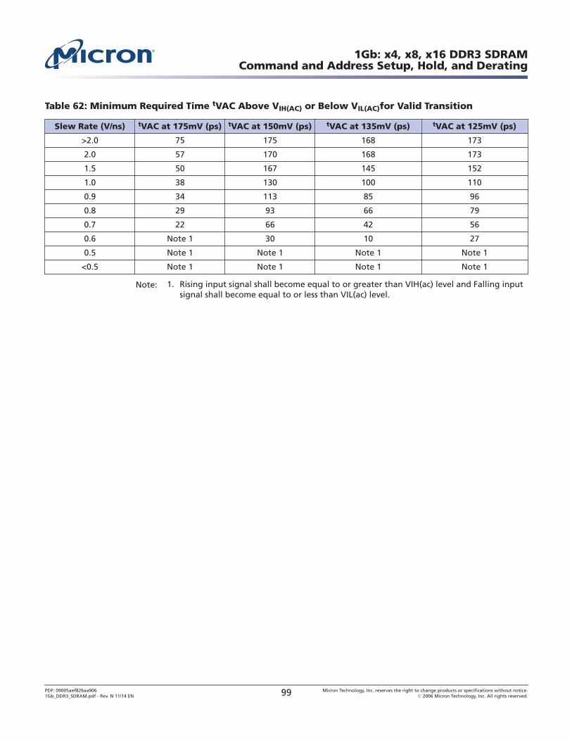
Table 62: Minimum Required Time tVAC Above VIH(AC) or Below VIL(AC)for Valid Transition
Slew Rate (V/ns) tVAC at 175mV (ps) tVAC at 150mV (ps) tVAC at 135mV (ps) tVAC at 125mV (ps)
>2.0 75 175 168 173
2.0 57 170 168 173
1.5 50 167 145 152
1.0 38 130 100 110
0.9 34 113 85 96
0.8 29 93 66 79
0.7 22 66 42 56
0.6 Note 1 30 10 27
0.5 Note 1 Note 1 Note 1 Note 1
<0.5 Note 1 Note 1 Note 1 Note 1
Note: 1. Rising input signal shall become equal to or greater than VIH(ac) level and Falling inputsignal shall become equal to or less than VIL(ac) level.
1Gb: x4, x8, x16 DDR3 SDRAMCommand and Address Setup, Hold, and Derating
PDF: 09005aef826aa9061Gb_DDR3_SDRAM.pdf - Rev. N 11/14 EN 99 Micron Technology, Inc. reserves the right to change products or specifications without notice.
© 2006 Micron Technology, Inc. All rights reserved.
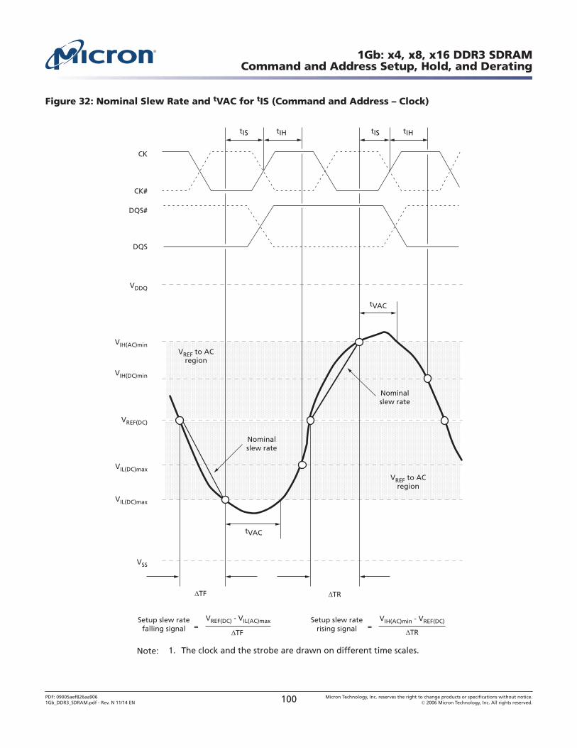
Figure 32: Nominal Slew Rate and tVAC for tIS (Command and Address – Clock)
VSS
Setup slew raterising signal
Setup slew ratefalling signal
ΔTF ΔTR
= =
VDDQ
VIH(AC)min
VIH(DC)min
VREF(DC)
VIL(DC)max
VIL(DC)max
Nominalslew rate
VREF to ACregion
tVAC
tVAC
DQS
DQS#
CK#
CK
tIS tIH tIS tIH
Nominalslew rate
VREF to ACregion
VREF(DC) - VIL(AC)max
ΔTF
VIH(AC)min - VREF(DC)
ΔTR
Note: 1. The clock and the strobe are drawn on different time scales.
1Gb: x4, x8, x16 DDR3 SDRAMCommand and Address Setup, Hold, and Derating
PDF: 09005aef826aa9061Gb_DDR3_SDRAM.pdf - Rev. N 11/14 EN 100 Micron Technology, Inc. reserves the right to change products or specifications without notice.
© 2006 Micron Technology, Inc. All rights reserved.
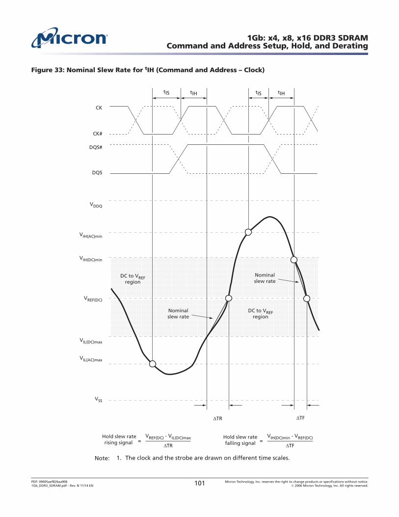
Figure 33: Nominal Slew Rate for tIH (Command and Address – Clock)
VSS
Hold slew ratefalling signal
Hold slew raterising signal
ΔTR ΔTF
= =
VDDQ
VIH(AC)min
VIH(DC)min
VREF(DC)
VIL(DC)max
VIL(AC)max
Nominalslew rate
DC to VREFregion
DQS
DQS#
CK#
CK
tIS tIH tIS tIH
DC to VREFregion
Nominalslew rate
VREF(DC) - VIL(DC)max
ΔTR
VIH(DC)min - VREF(DC)
ΔTF
Note: 1. The clock and the strobe are drawn on different time scales.
1Gb: x4, x8, x16 DDR3 SDRAMCommand and Address Setup, Hold, and Derating
PDF: 09005aef826aa9061Gb_DDR3_SDRAM.pdf - Rev. N 11/14 EN 101 Micron Technology, Inc. reserves the right to change products or specifications without notice.
© 2006 Micron Technology, Inc. All rights reserved.
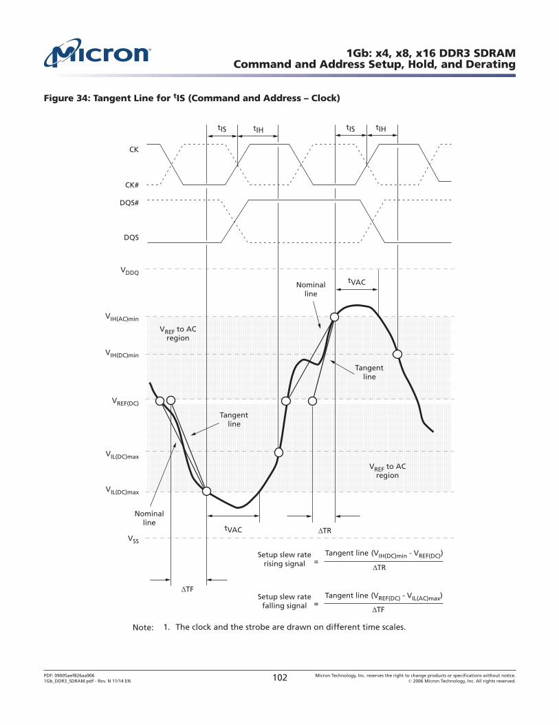
Figure 34: Tangent Line for tIS (Command and Address – Clock)
VSS
Setup slew raterising signal
Setup slew ratefalling signal =
=
VDDQ
VIH(AC)min
VIH(DC)min
VREF(DC)
VIL(DC)max
VIL(DC)max
Tangentline
VREF to ACregion
Nominalline
tVAC
tVAC
DQS
DQS#
CK#
CK
tIS tIH tIS tIH
VREF to ACregion
Tangentline
Nominalline
Tangent line (VIH(DC)min - VREF(DC))
Tangent line (VREF(DC) - VIL(AC)max)
ΔTR
ΔTR
ΔTF
ΔTF
Note: 1. The clock and the strobe are drawn on different time scales.
1Gb: x4, x8, x16 DDR3 SDRAMCommand and Address Setup, Hold, and Derating
PDF: 09005aef826aa9061Gb_DDR3_SDRAM.pdf - Rev. N 11/14 EN 102 Micron Technology, Inc. reserves the right to change products or specifications without notice.
© 2006 Micron Technology, Inc. All rights reserved.
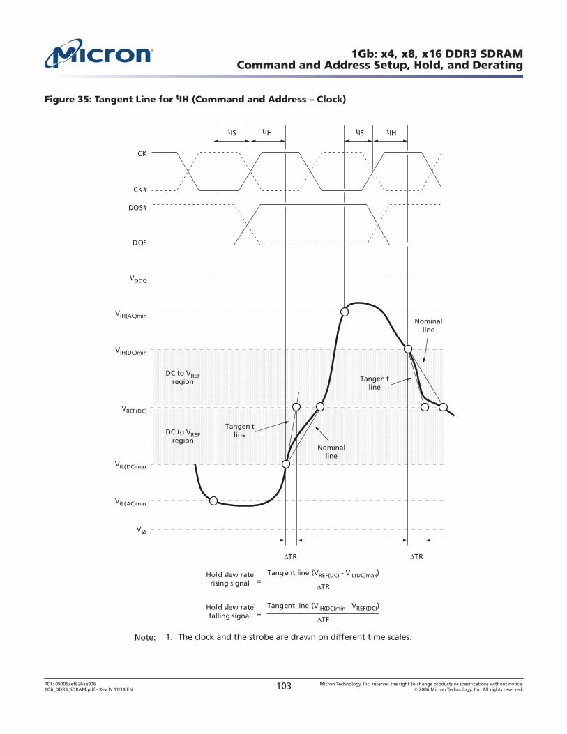
Figure 35: Tangent Line for tIH (Command and Address – Clock)
VSS
Hold slew ratefalling signal =
VDDQ
VIH(AC)min
VIH(DC)min
VREF(DC)
VIL(DC)max
VIL(AC)max
Tangen tline
DC to VREFregion
Hold slew raterising signal =
DQS
DQS#
CK#
CK
tIS tIH tIS tIH
DC to VREFregion
Tangen tline
Nominalline
Nominalline
Tangent line (VREF(DC) - VIL(DC)max)
Tangent line (VIH(DC)min - VREF(DC))
ΔTR ΔTR
ΔTR
ΔTF
Note: 1. The clock and the strobe are drawn on different time scales.
1Gb: x4, x8, x16 DDR3 SDRAMCommand and Address Setup, Hold, and Derating
PDF: 09005aef826aa9061Gb_DDR3_SDRAM.pdf - Rev. N 11/14 EN 103 Micron Technology, Inc. reserves the right to change products or specifications without notice.
© 2006 Micron Technology, Inc. All rights reserved.
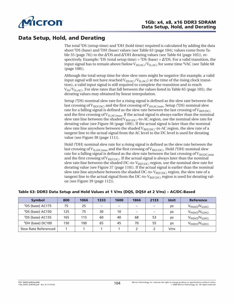
Data Setup, Hold, and DeratingThe total tDS (setup time) and tDH (hold time) required is calculated by adding the datasheet tDS (base) and tDH (base) values (see Table 63 (page 104); values come from Ta-ble 55 (page 76)) to the ΔtDS and ΔtDH derating values (see Table 64 (page 105)), re-spectively. Example: tDS (total setup time) = tDS (base) + ΔtDS. For a valid transition, theinput signal has to remain above/below VIH(AC)/VIL(AC) for some time tVAC (see Table 68(page 108)).
Although the total setup time for slow slew rates might be negative (for example, a validinput signal will not have reached VIH(AC)/VIL(AC)) at the time of the rising clock transi-tion), a valid input signal is still required to complete the transition and to reachVIH/VIL(AC). For slew rates that fall between the values listed in Table 65 (page 105), thederating values may obtained by linear interpolation.
Setup (tDS) nominal slew rate for a rising signal is defined as the slew rate between thelast crossing of VREF(DC) and the first crossing of VIH(AC)min. Setup (tDS) nominal slewrate for a falling signal is defined as the slew rate between the last crossing of VREF(DC)and the first crossing of VIL(AC)max. If the actual signal is always earlier than the nominalslew rate line between the shaded VREF(DC)-to-AC region, use the nominal slew rate forderating value (see Figure 36 (page 109)). If the actual signal is later than the nominalslew rate line anywhere between the shaded VREF(DC)-to-AC region, the slew rate of atangent line to the actual signal from the AC level to the DC level is used for deratingvalue (see Figure 38 (page 111)).
Hold (tDH) nominal slew rate for a rising signal is defined as the slew rate between thelast crossing of VIL(DC)max and the first crossing of VREF(DC). Hold (tDH) nominal slewrate for a falling signal is defined as the slew rate between the last crossing of VIH(DC)minand the first crossing of VREF(DC). If the actual signal is always later than the nominalslew rate line between the shaded DC-to-VREF(DC) region, use the nominal slew rate forderating value (see Figure 37 (page 110)). If the actual signal is earlier than the nominalslew rate line anywhere between the shaded DC-to-VREF(DC) region, the slew rate of atangent line to the actual signal from the DC-to-VREF(DC) region is used for derating val-ue (see Figure 39 (page 112)).
Table 63: DDR3 Data Setup and Hold Values at 1 V/ns (DQS, DQS# at 2 V/ns) – AC/DC-Based
Symbol 800 1066 1333 1600 1866 2133 Unit ReferencetDS (base) AC175 75 25 – – – – ps VIH(AC)/VIL(AC)
tDS (base) AC150 125 75 30 10 – – ps VIH(AC)/VIL(AC)
tDS (base) AC135 165 115 60 40 68 53 ps VIH(AC)/VIL(AC)
tDH (base) DC100 150 100 65 45 70 55 ps VIH(DC)/VIL(DC)
Slew Rate Referenced 1 1 1 1 2 2 V/ns
1Gb: x4, x8, x16 DDR3 SDRAMData Setup, Hold, and Derating
PDF: 09005aef826aa9061Gb_DDR3_SDRAM.pdf - Rev. N 11/14 EN 104 Micron Technology, Inc. reserves the right to change products or specifications without notice.
© 2006 Micron Technology, Inc. All rights reserved.
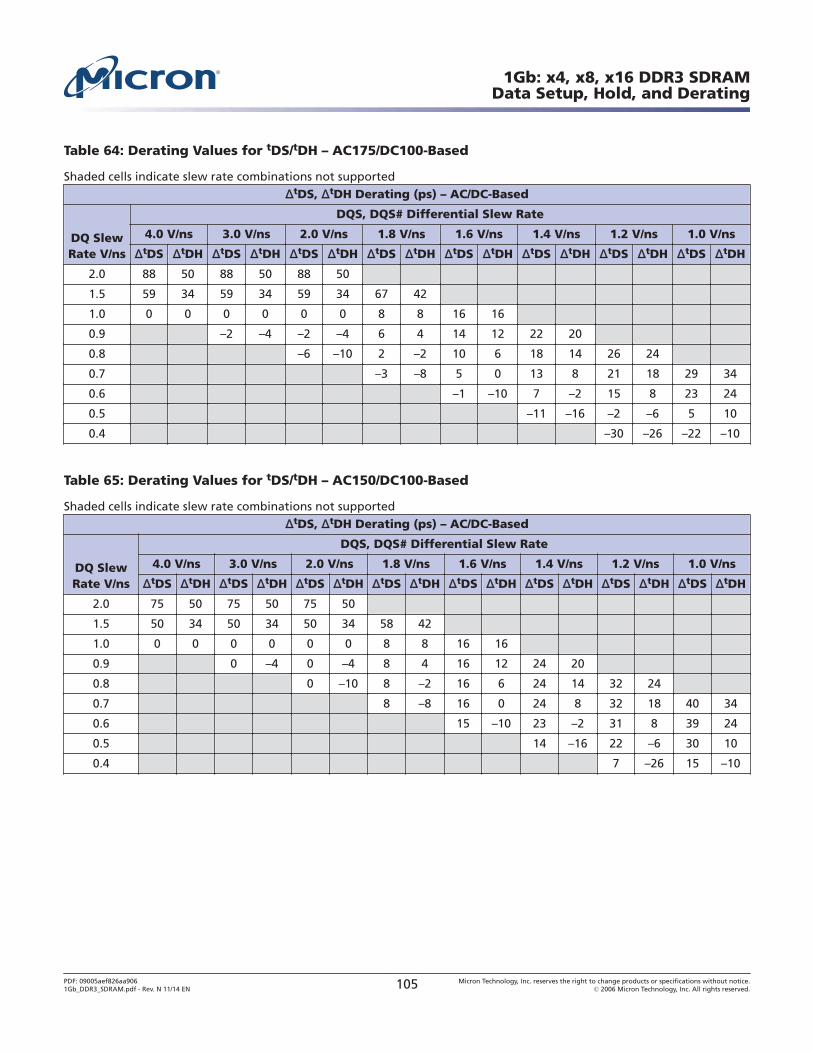
Table 64: Derating Values for tDS/tDH – AC175/DC100-Based
Shaded cells indicate slew rate combinations not supportedΔΔtDS, ΔtDH Derating (ps) – AC/DC-Based
DQ SlewRate V/ns
DQS, DQS# Differential Slew Rate
4.0 V/ns 3.0 V/ns 2.0 V/ns 1.8 V/ns 1.6 V/ns 1.4 V/ns 1.2 V/ns 1.0 V/ns
ΔtDS ΔtDH ΔtDS ΔtDH ΔtDS ΔtDH ΔtDS ΔtDH ΔtDS ΔtDH ΔtDS ΔtDH ΔtDS ΔtDH ΔtDS ΔtDH
2.0 88 50 88 50 88 50
1.5 59 34 59 34 59 34 67 42
1.0 0 0 0 0 0 0 8 8 16 16
0.9 –2 –4 –2 –4 6 4 14 12 22 20
0.8 –6 –10 2 –2 10 6 18 14 26 24
0.7 –3 –8 5 0 13 8 21 18 29 34
0.6 –1 –10 7 –2 15 8 23 24
0.5 –11 –16 –2 –6 5 10
0.4 –30 –26 –22 –10
Table 65: Derating Values for tDS/tDH – AC150/DC100-Based
Shaded cells indicate slew rate combinations not supportedΔtDS, ΔtDH Derating (ps) – AC/DC-Based
DQ SlewRate V/ns
DQS, DQS# Differential Slew Rate
4.0 V/ns 3.0 V/ns 2.0 V/ns 1.8 V/ns 1.6 V/ns 1.4 V/ns 1.2 V/ns 1.0 V/ns
ΔtDS ΔtDH ΔtDS ΔtDH ΔtDS ΔtDH ΔtDS ΔtDH ΔtDS ΔtDH ΔtDS ΔtDH ΔtDS ΔtDH ΔtDS ΔtDH
2.0 75 50 75 50 75 50
1.5 50 34 50 34 50 34 58 42
1.0 0 0 0 0 0 0 8 8 16 16
0.9 0 –4 0 –4 8 4 16 12 24 20
0.8 0 –10 8 –2 16 6 24 14 32 24
0.7 8 –8 16 0 24 8 32 18 40 34
0.6 15 –10 23 –2 31 8 39 24
0.5 14 –16 22 –6 30 10
0.4 7 –26 15 –10
1Gb: x4, x8, x16 DDR3 SDRAMData Setup, Hold, and Derating
PDF: 09005aef826aa9061Gb_DDR3_SDRAM.pdf - Rev. N 11/14 EN 105 Micron Technology, Inc. reserves the right to change products or specifications without notice.
© 2006 Micron Technology, Inc. All rights reserved.
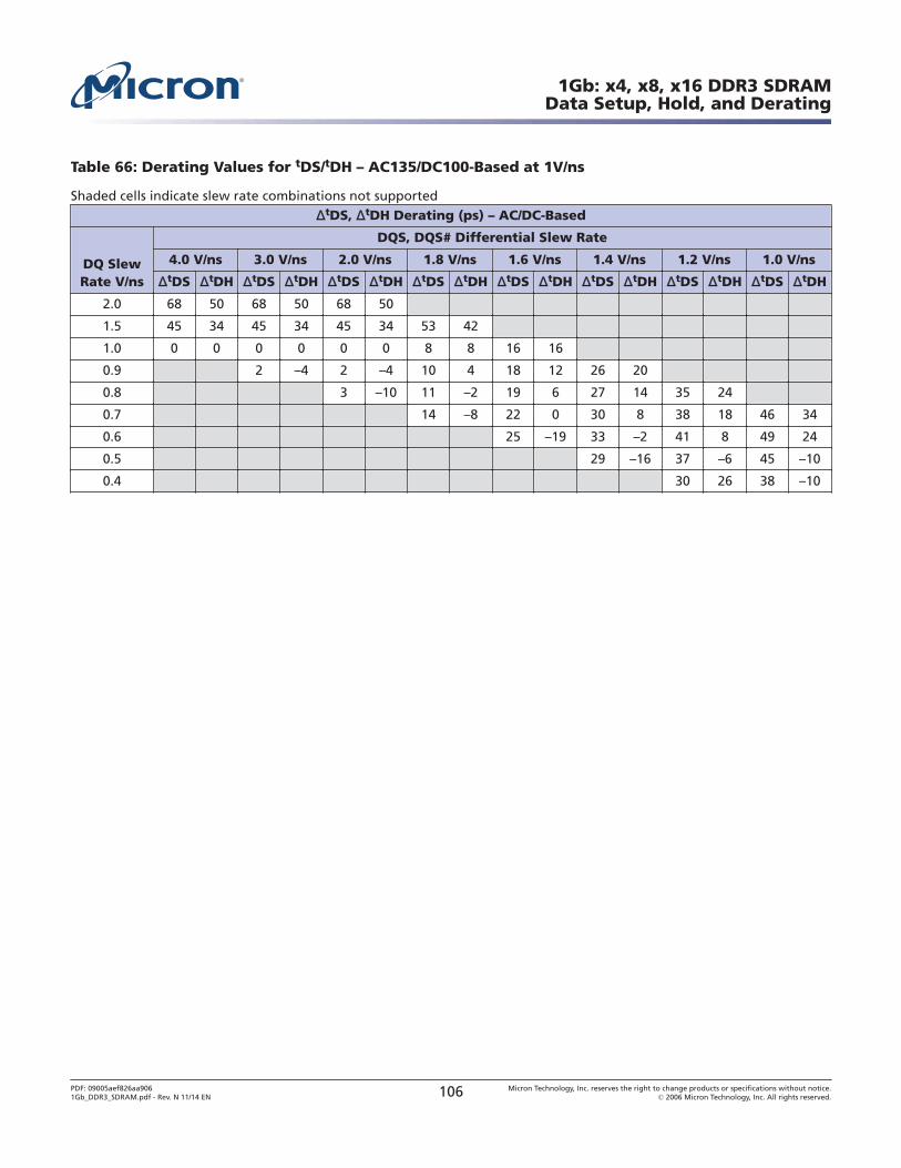
Table 66: Derating Values for tDS/tDH – AC135/DC100-Based at 1V/ns
Shaded cells indicate slew rate combinations not supportedΔΔtDS, ΔtDH Derating (ps) – AC/DC-Based
DQ SlewRate V/ns
DQS, DQS# Differential Slew Rate
4.0 V/ns 3.0 V/ns 2.0 V/ns 1.8 V/ns 1.6 V/ns 1.4 V/ns 1.2 V/ns 1.0 V/ns
ΔtDS ΔtDH ΔtDS ΔtDH ΔtDS ΔtDH ΔtDS ΔtDH ΔtDS ΔtDH ΔtDS ΔtDH ΔtDS ΔtDH ΔtDS ΔtDH
2.0 68 50 68 50 68 50
1.5 45 34 45 34 45 34 53 42
1.0 0 0 0 0 0 0 8 8 16 16
0.9 2 –4 2 –4 10 4 18 12 26 20
0.8 3 –10 11 –2 19 6 27 14 35 24
0.7 14 –8 22 0 30 8 38 18 46 34
0.6 25 –19 33 –2 41 8 49 24
0.5 29 –16 37 –6 45 –10
0.4 30 26 38 –10
1Gb: x4, x8, x16 DDR3 SDRAMData Setup, Hold, and Derating
PDF: 09005aef826aa9061Gb_DDR3_SDRAM.pdf - Rev. N 11/14 EN 106 Micron Technology, Inc. reserves the right to change products or specifications without notice.
© 2006 Micron Technology, Inc. All rights reserved.
Tab
le 6
7: D
era
tin
g V
alu
es
for
t DS/tD
H –
AC
135/D
C100-B
ase
d a
t 2V
/ns
Shad
ed c
ells
ind
icat
e sl
ew r
ate
com
bin
atio
ns
no
t su
pp
ort
edΔΔt
DS,
ΔtD
H D
era
tin
g (
ps)
– A
C/D
C-B
ase
dDQ Slew Rate V/ns
DQ
S, D
QS# D
iffe
ren
tial
Sle
w R
ate
8.0
V/n
s7.0
V/n
s6.0
V/n
s5.0
V/n
s4.0
V/n
s3.0
V/n
s2.0
V/n
s1.8
V/n
s1.6
V/n
s1.4
V/n
s1.2
V/n
s1.0
V/n
s
Δt D
SΔ
t DH
Δt D
SΔ
t DH
Δt D
SΔ
t DH
Δt D
SΔ
t DH
Δt D
SΔ
t DH
Δt D
SΔ
t DH
Δt D
SΔ
t DH
Δt D
SΔ
t DH
Δt D
SΔ
t DH
Δt D
SΔ
t DH
Δt D
SΔ
t DH
Δt D
SΔ
t DH
4.0
3425
3425
3425
3.5
2921
2921
2921
2921
3.0
2317
2317
2317
2317
2317
2.5
1410
1410
1410
1410
1410
2.0
00
00
00
00
00
1.5
–23
–17
–23
–17
–23
–17
–23
–17
–15
–19
1.0
–68
–50
–68
–50
–68
–50
–60
–42
–52
–34
0.9
–66
–54
–66
–54
–58
–46
–50
–38
–42
–30
0.8
–64
60–5
6–5
2–4
8–4
0–4
0–3
6–3
2–2
6
0.7
–53
–59
–45
–51
–37
–43
–29
–33
–21
–17
0.6
–43
–61
–35
–53
–27
–43
–19
–27
0.5
–39
–66
–31
–56
–23
–40
0.4
–38
–76
–30
–60
1Gb: x4, x8, x16 DDR3 SDRAMData Setup, Hold, and Derating
PDF: 09005aef826aa9061Gb_DDR3_SDRAM.pdf - Rev. N 11/14 EN 107 Micron Technology, Inc. reserves the right to change products or specifications without notice.
© 2006 Micron Technology, Inc. All rights reserved.
Table 68: Required Minimum Time tVAC Above VIH(AC) (Below VIL(AC)) for Valid DQ Transition
SlewRate
(V/ns)
tVAC at 175mV (ps) tVAC at 150mV (ps) tVAC at 135mV (ps)
DDR3-800/1066 DDR3-800/1066/1333/1600 DDR3-800/1066/1333/1600 DDR3-1866 DDR3-2133
>2.0 75 105 113 93 73
2.0 57 105 113 93 73
1.5 50 80 90 70 50
1.0 38 30 45 25 5
0.9 34 13 30 Note 1 Note 1
0.8 29 Note 1 11 Note 1 Note 1
0.7 Note 1 Note 1 Note 1 Note 1 Note 1
0.6 Note 1 Note 1 Note 1 Note 1 Note 1
0.5 Note 1 Note 1 Note 1 Note 1 Note 1
<0.5 Note 1 Note 1 Note 1 Note 1 Note 1
Note: 1. Rising input signal shall become equal to or greater than VIH(ac) level and Falling inputsignal shall become equal to or less than VIL(ac) level.
1Gb: x4, x8, x16 DDR3 SDRAMData Setup, Hold, and Derating
PDF: 09005aef826aa9061Gb_DDR3_SDRAM.pdf - Rev. N 11/14 EN 108 Micron Technology, Inc. reserves the right to change products or specifications without notice.
© 2006 Micron Technology, Inc. All rights reserved.
Figure 36: Nominal Slew Rate and tVAC for tDS (DQ – Strobe)
VSS
Setup slew raterising signal
Setup slew ratefalling signal
ΔTF ΔTR
= =
VDDQ
VIH(AC)min
VIH(DC)min
VREF(DC)
VIL(DC)max
VIL(AC)max
Nominalslew rate
VREF to AC region
tVAC
tVAC
tDHtDS
DQS
DQS#
tDHtDS
CK#
CK
VREF to AC region
Nominalslew rate
VIH(AC)min - VREF(DC)
ΔTR
VREF(DC) - VIL(AC)max
ΔTF
Note: 1. The clock and the strobe are drawn on different time scales.
1Gb: x4, x8, x16 DDR3 SDRAMData Setup, Hold, and Derating
PDF: 09005aef826aa9061Gb_DDR3_SDRAM.pdf - Rev. N 11/14 EN 109 Micron Technology, Inc. reserves the right to change products or specifications without notice.
© 2006 Micron Technology, Inc. All rights reserved.
Figure 37: Nominal Slew Rate for tDH (DQ – Strobe)
VSS
Hold slew ratefalling signal
Hold slew raterising signal = =
VDDQ
VIH(AC)min
VIH(DC)min
VREF(DC)
VIL(DC)max
VIL(AC)max
Nominal slew rateDC to VREF
region
tDHtDS
DQS
DQS#
tDHtDS
CK#
CK
DC to VREFregion
Nominal slew rate
VREF(DC) - VIL(DC)max VIL(DC)min - VREF(DC)
ΔTR ΔTF
ΔTFΔTR
Note: 1. The clock and the strobe are drawn on different time scales.
1Gb: x4, x8, x16 DDR3 SDRAMData Setup, Hold, and Derating
PDF: 09005aef826aa9061Gb_DDR3_SDRAM.pdf - Rev. N 11/14 EN 110 Micron Technology, Inc. reserves the right to change products or specifications without notice.
© 2006 Micron Technology, Inc. All rights reserved.
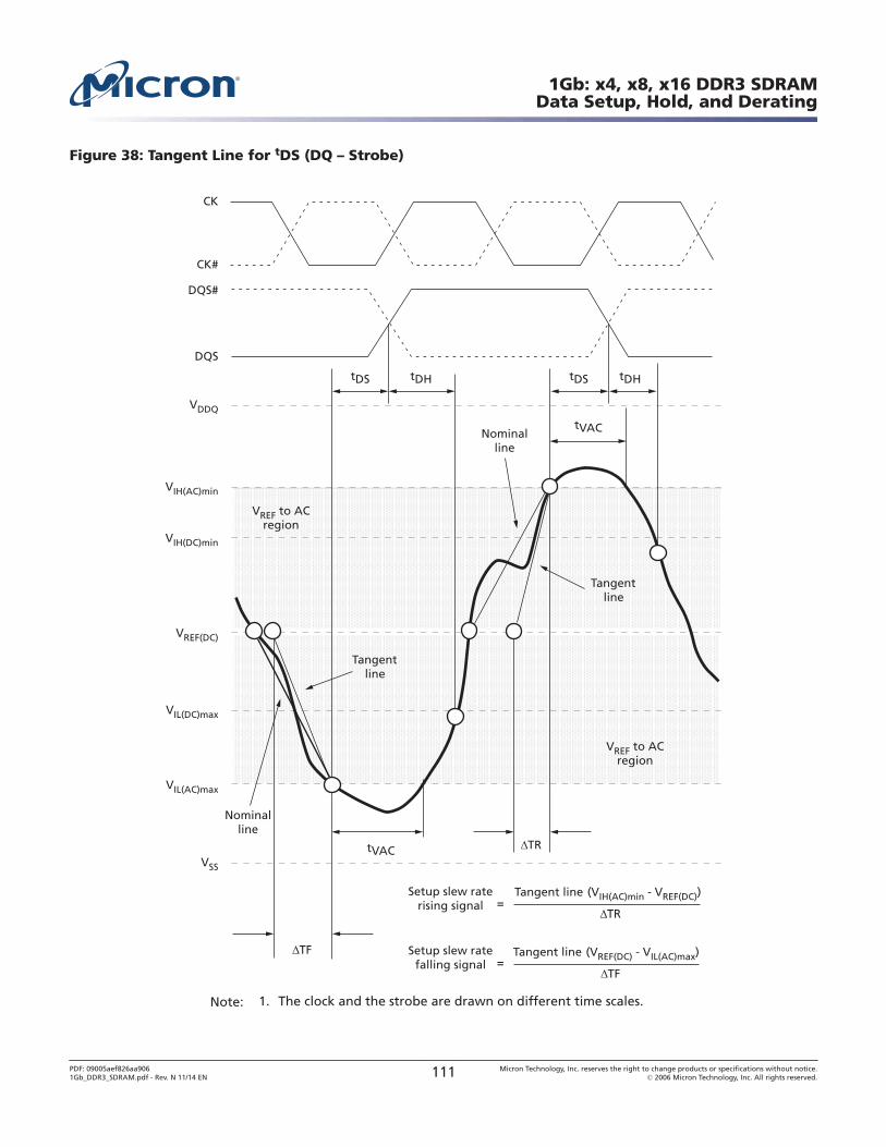
Figure 38: Tangent Line for tDS (DQ – Strobe)
VSS
Setup slew raterising signal
Setup slew ratefalling signal =
=
VDDQ
VIH(AC)min
VIH(DC)min
VREF(DC)
VIL(DC)max
VIL(AC)max
Tangentline
VREF to ACregion
Nominalline
tVAC
tVAC
tDHtDS
DQS
DQS#
tDHtDS
CK#
CK
VREF to ACregion
Tangentline
Nominalline
Tangent line (VREF(DC) - VIL(AC)max)
Tangent line (VIH(AC)min - VREF(DC))
ΔTR
ΔTR
ΔTF
ΔTF
Note: 1. The clock and the strobe are drawn on different time scales.
1Gb: x4, x8, x16 DDR3 SDRAMData Setup, Hold, and Derating
PDF: 09005aef826aa9061Gb_DDR3_SDRAM.pdf - Rev. N 11/14 EN 111 Micron Technology, Inc. reserves the right to change products or specifications without notice.
© 2006 Micron Technology, Inc. All rights reserved.
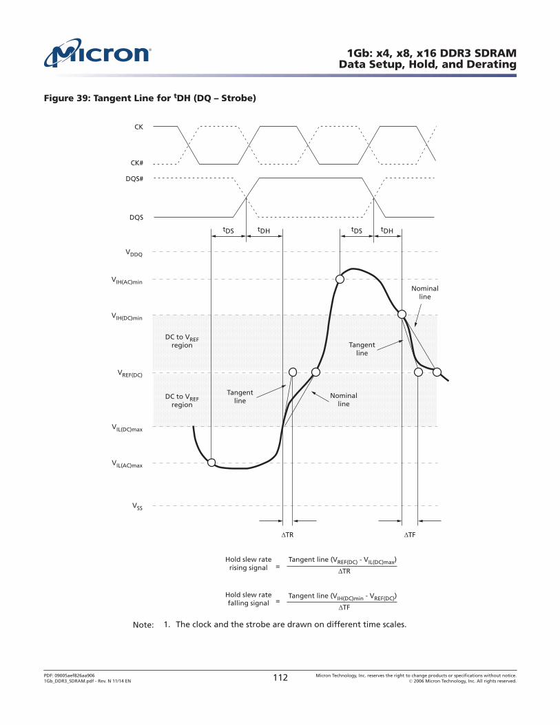
Figure 39: Tangent Line for tDH (DQ – Strobe)
VSS
Hold slew ratefalling signal
ΔTFΔTR
=
VDDQ
VIH(AC)min
VIH(DC)min
VREF(DC)
VIL(DC)max
VIL(AC)max
Tangentline
DC to VREFregion
Hold slew raterising signal =
DQS
DQS#
CK#
CK
DC to VREFregion
Tangentline
Nominalline
Nominalline
Tangent line (VIH(DC)min - VREF(DC))
ΔTF
Tangent line (VREF(DC) - VIL(DC)max)
ΔTR
tDS tDH tDS tDH
Note: 1. The clock and the strobe are drawn on different time scales.
1Gb: x4, x8, x16 DDR3 SDRAMData Setup, Hold, and Derating
PDF: 09005aef826aa9061Gb_DDR3_SDRAM.pdf - Rev. N 11/14 EN 112 Micron Technology, Inc. reserves the right to change products or specifications without notice.
© 2006 Micron Technology, Inc. All rights reserved.
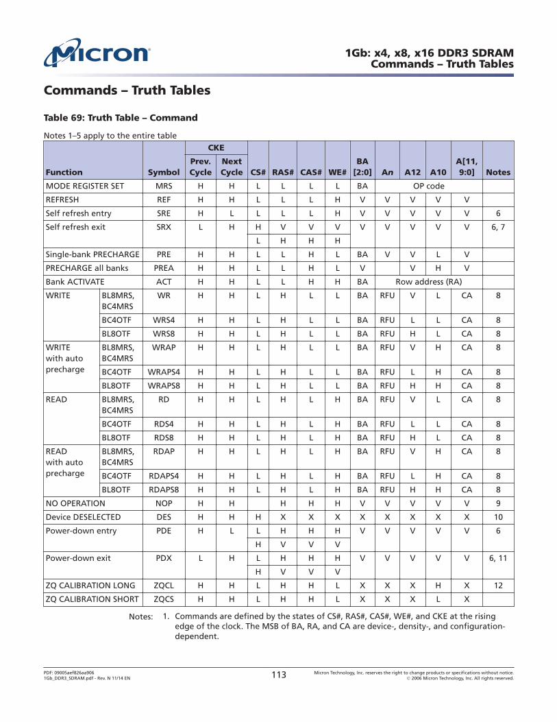
Commands – Truth Tables
Table 69: Truth Table – Command
Notes 1–5 apply to the entire table
Function Symbol
CKE
CS# RAS# CAS# WE#BA
[2:0] An A12 A10A[11,9:0] Notes
Prev.Cycle
NextCycle
MODE REGISTER SET MRS H H L L L L BA OP code
REFRESH REF H H L L L H V V V V V
Self refresh entry SRE H L L L L H V V V V V 6
Self refresh exit SRX L H H V V V V V V V V 6, 7
L H H H
Single-bank PRECHARGE PRE H H L L H L BA V V L V
PRECHARGE all banks PREA H H L L H L V V H V
Bank ACTIVATE ACT H H L L H H BA Row address (RA)
WRITE BL8MRS,BC4MRS
WR H H L H L L BA RFU V L CA 8
BC4OTF WRS4 H H L H L L BA RFU L L CA 8
BL8OTF WRS8 H H L H L L BA RFU H L CA 8
WRITEwith autoprecharge
BL8MRS,BC4MRS
WRAP H H L H L L BA RFU V H CA 8
BC4OTF WRAPS4 H H L H L L BA RFU L H CA 8
BL8OTF WRAPS8 H H L H L L BA RFU H H CA 8
READ BL8MRS,BC4MRS
RD H H L H L H BA RFU V L CA 8
BC4OTF RDS4 H H L H L H BA RFU L L CA 8
BL8OTF RDS8 H H L H L H BA RFU H L CA 8
READwith autoprecharge
BL8MRS,BC4MRS
RDAP H H L H L H BA RFU V H CA 8
BC4OTF RDAPS4 H H L H L H BA RFU L H CA 8
BL8OTF RDAPS8 H H L H L H BA RFU H H CA 8
NO OPERATION NOP H H H H H V V V V V 9
Device DESELECTED DES H H H X X X X X X X X 10
Power-down entry PDE H L L H H H V V V V V 6
H V V V
Power-down exit PDX L H L H H H V V V V V 6, 11
H V V V
ZQ CALIBRATION LONG ZQCL H H L H H L X X X H X 12
ZQ CALIBRATION SHORT ZQCS H H L H H L X X X L X
Notes: 1. Commands are defined by the states of CS#, RAS#, CAS#, WE#, and CKE at the risingedge of the clock. The MSB of BA, RA, and CA are device-, density-, and configuration-dependent.
1Gb: x4, x8, x16 DDR3 SDRAMCommands – Truth Tables
PDF: 09005aef826aa9061Gb_DDR3_SDRAM.pdf - Rev. N 11/14 EN 113 Micron Technology, Inc. reserves the right to change products or specifications without notice.
© 2006 Micron Technology, Inc. All rights reserved.
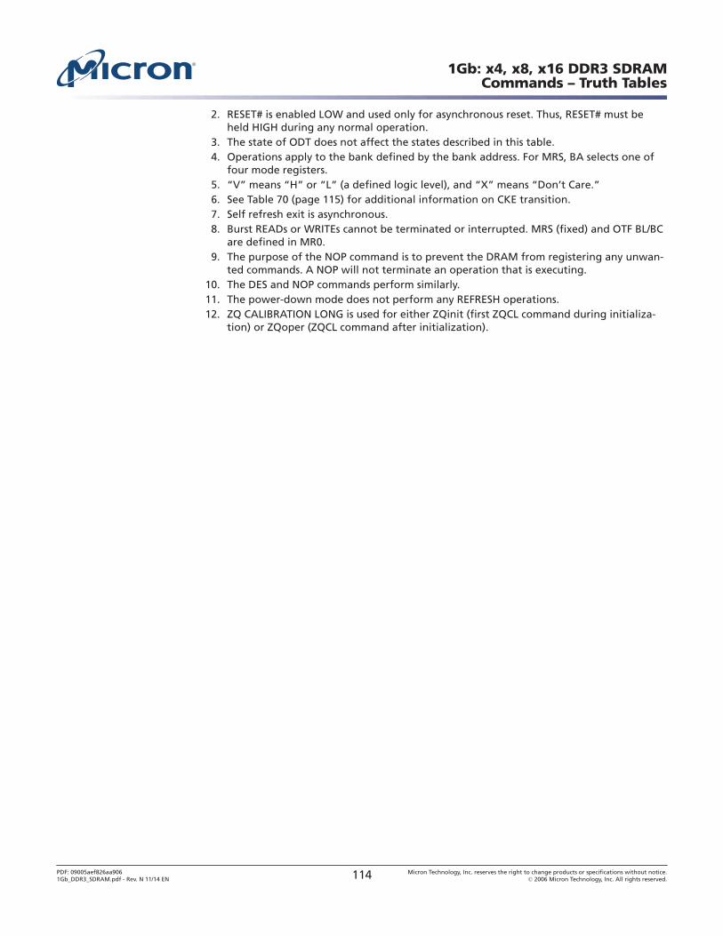
2. RESET# is enabled LOW and used only for asynchronous reset. Thus, RESET# must beheld HIGH during any normal operation.
3. The state of ODT does not affect the states described in this table.4. Operations apply to the bank defined by the bank address. For MRS, BA selects one of
four mode registers.5. “V” means “H” or “L” (a defined logic level), and “X” means “Don’t Care.”6. See Table 70 (page 115) for additional information on CKE transition.7. Self refresh exit is asynchronous.8. Burst READs or WRITEs cannot be terminated or interrupted. MRS (fixed) and OTF BL/BC
are defined in MR0.9. The purpose of the NOP command is to prevent the DRAM from registering any unwan-
ted commands. A NOP will not terminate an operation that is executing.10. The DES and NOP commands perform similarly.11. The power-down mode does not perform any REFRESH operations.12. ZQ CALIBRATION LONG is used for either ZQinit (first ZQCL command during initializa-
tion) or ZQoper (ZQCL command after initialization).
1Gb: x4, x8, x16 DDR3 SDRAMCommands – Truth Tables
PDF: 09005aef826aa9061Gb_DDR3_SDRAM.pdf - Rev. N 11/14 EN 114 Micron Technology, Inc. reserves the right to change products or specifications without notice.
© 2006 Micron Technology, Inc. All rights reserved.
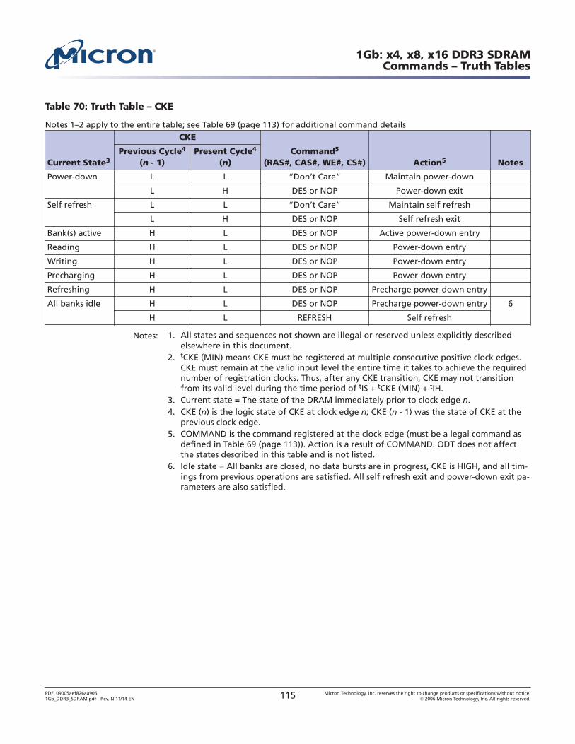
Table 70: Truth Table – CKE
Notes 1–2 apply to the entire table; see Table 69 (page 113) for additional command details
Current State3
CKE
Command5
(RAS#, CAS#, WE#, CS#) Action5 NotesPrevious Cycle4
(n - 1)Present Cycle4
(n)
Power-down L L “Don’t Care” Maintain power-down
L H DES or NOP Power-down exit
Self refresh L L “Don’t Care” Maintain self refresh
L H DES or NOP Self refresh exit
Bank(s) active H L DES or NOP Active power-down entry
Reading H L DES or NOP Power-down entry
Writing H L DES or NOP Power-down entry
Precharging H L DES or NOP Power-down entry
Refreshing H L DES or NOP Precharge power-down entry
All banks idle H L DES or NOP Precharge power-down entry 6
H L REFRESH Self refresh
Notes: 1. All states and sequences not shown are illegal or reserved unless explicitly describedelsewhere in this document.
2. tCKE (MIN) means CKE must be registered at multiple consecutive positive clock edges.CKE must remain at the valid input level the entire time it takes to achieve the requirednumber of registration clocks. Thus, after any CKE transition, CKE may not transitionfrom its valid level during the time period of tIS + tCKE (MIN) + tIH.
3. Current state = The state of the DRAM immediately prior to clock edge n.4. CKE (n) is the logic state of CKE at clock edge n; CKE (n - 1) was the state of CKE at the
previous clock edge.5. COMMAND is the command registered at the clock edge (must be a legal command as
defined in Table 69 (page 113)). Action is a result of COMMAND. ODT does not affectthe states described in this table and is not listed.
6. Idle state = All banks are closed, no data bursts are in progress, CKE is HIGH, and all tim-ings from previous operations are satisfied. All self refresh exit and power-down exit pa-rameters are also satisfied.
1Gb: x4, x8, x16 DDR3 SDRAMCommands – Truth Tables
PDF: 09005aef826aa9061Gb_DDR3_SDRAM.pdf - Rev. N 11/14 EN 115 Micron Technology, Inc. reserves the right to change products or specifications without notice.
© 2006 Micron Technology, Inc. All rights reserved.
Commands
DESELECT
The DESELT (DES) command (CS# HIGH) prevents new commands from being execu-ted by the DRAM. Operations already in progress are not affected.
NO OPERATION
The NO OPERATION (NOP) command (CS# LOW) prevents unwanted commands frombeing registered during idle or wait states. Operations already in progress are not affec-ted.
ZQ CALIBRATION LONG
The ZQ CALIBRATION LONG (ZQCL) command is used to perform the initial calibra-tion during a power-up initialization and reset sequence (see Figure 48 (page 132)).This command may be issued at any time by the controller, depending on the systemenvironment. The ZQCL command triggers the calibration engine inside the DRAM. Af-ter calibration is achieved, the calibrated values are transferred from the calibration en-gine to the DRAM I/O, which are reflected as updated RON and ODT values.
The DRAM is allowed a timing window defined by either tZQinit or tZQoper to performa full calibration and transfer of values. When ZQCL is issued during the initializationsequence, the timing parameter tZQinit must be satisfied. When initialization is com-plete, subsequent ZQCL commands require the timing parameter tZQoper to be satis-fied.
ZQ CALIBRATION SHORT
The ZQ CALIBRATION SHORT (ZQCS) command is used to perform periodic calibra-tions to account for small voltage and temperature variations. A shorter timing windowis provided to perform the reduced calibration and transfer of values as defined by tim-ing parameter tZQCS. A ZQCS command can effectively correct a minimum of 0.5% RONand RTT impedance error within 64 clock cycles, assuming the maximum sensitivitiesspecified in Table 41 (page 63) and Table 42 (page 63).
ACTIVATE
The ACTIVATE command is used to open (or activate) a row in a particular bank for asubsequent access. The value on the BA[2:0] inputs selects the bank, and the addressprovided on inputs A[n:0] selects the row. This row remains open (or active) for accessesuntil a PRECHARGE command is issued to that bank.
A PRECHARGE command must be issued before opening a different row in the samebank.
READ
The READ command is used to initiate a burst read access to an active row. The addressprovided on inputs A[2:0] selects the starting column address, depending on the burstlength and burst type selected (see Burst Order table for additional information). Thevalue on input A10 determines whether auto precharge is used. If auto precharge is se-lected, the row being accessed will be precharged at the end of the READ burst. If auto
1Gb: x4, x8, x16 DDR3 SDRAMCommands
PDF: 09005aef826aa9061Gb_DDR3_SDRAM.pdf - Rev. N 11/14 EN 116 Micron Technology, Inc. reserves the right to change products or specifications without notice.
© 2006 Micron Technology, Inc. All rights reserved.
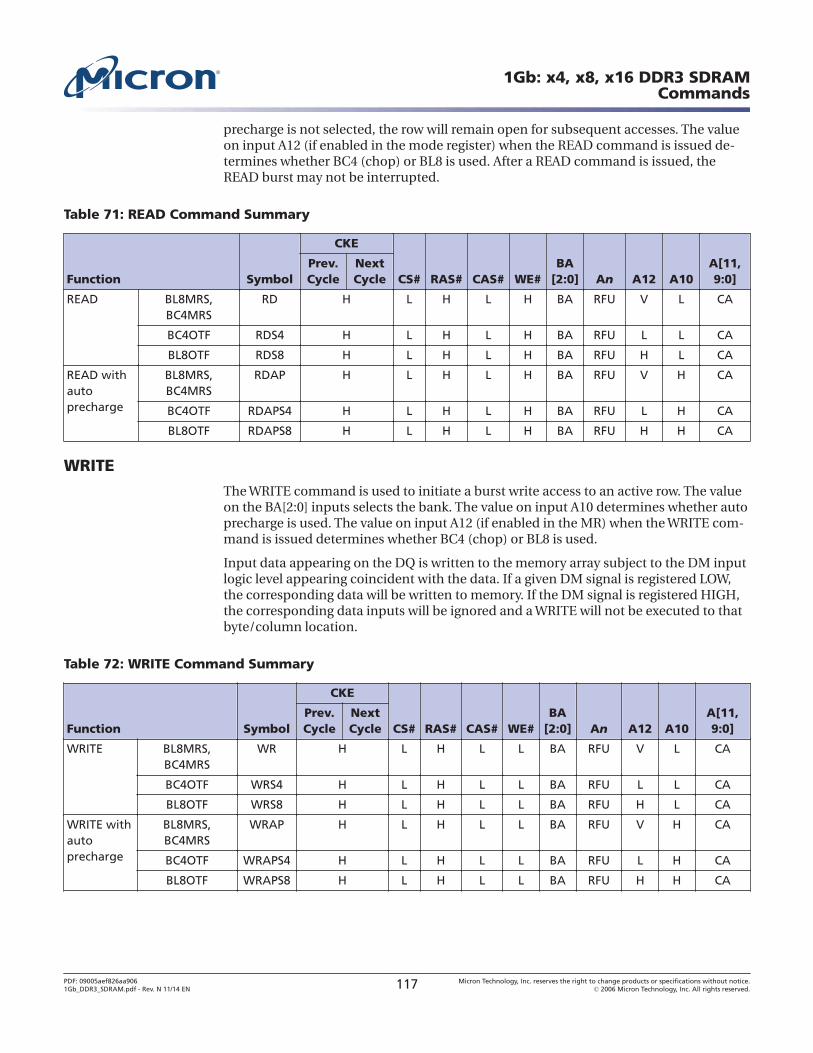
precharge is not selected, the row will remain open for subsequent accesses. The valueon input A12 (if enabled in the mode register) when the READ command is issued de-termines whether BC4 (chop) or BL8 is used. After a READ command is issued, theREAD burst may not be interrupted.
Table 71: READ Command Summary
Function Symbol
CKE
CS# RAS# CAS# WE#BA
[2:0] An A12 A10A[11,9:0]
Prev.Cycle
NextCycle
READ BL8MRS,BC4MRS
RD H L H L H BA RFU V L CA
BC4OTF RDS4 H L H L H BA RFU L L CA
BL8OTF RDS8 H L H L H BA RFU H L CA
READ withautoprecharge
BL8MRS,BC4MRS
RDAP H L H L H BA RFU V H CA
BC4OTF RDAPS4 H L H L H BA RFU L H CA
BL8OTF RDAPS8 H L H L H BA RFU H H CA
WRITE
The WRITE command is used to initiate a burst write access to an active row. The valueon the BA[2:0] inputs selects the bank. The value on input A10 determines whether autoprecharge is used. The value on input A12 (if enabled in the MR) when the WRITE com-mand is issued determines whether BC4 (chop) or BL8 is used.
Input data appearing on the DQ is written to the memory array subject to the DM inputlogic level appearing coincident with the data. If a given DM signal is registered LOW,the corresponding data will be written to memory. If the DM signal is registered HIGH,the corresponding data inputs will be ignored and a WRITE will not be executed to thatbyte/column location.
Table 72: WRITE Command Summary
Function Symbol
CKE
CS# RAS# CAS# WE#BA
[2:0] An A12 A10A[11,9:0]
Prev.Cycle
NextCycle
WRITE BL8MRS,BC4MRS
WR H L H L L BA RFU V L CA
BC4OTF WRS4 H L H L L BA RFU L L CA
BL8OTF WRS8 H L H L L BA RFU H L CA
WRITE withautoprecharge
BL8MRS,BC4MRS
WRAP H L H L L BA RFU V H CA
BC4OTF WRAPS4 H L H L L BA RFU L H CA
BL8OTF WRAPS8 H L H L L BA RFU H H CA
1Gb: x4, x8, x16 DDR3 SDRAMCommands
PDF: 09005aef826aa9061Gb_DDR3_SDRAM.pdf - Rev. N 11/14 EN 117 Micron Technology, Inc. reserves the right to change products or specifications without notice.
© 2006 Micron Technology, Inc. All rights reserved.
PRECHARGE
The PRECHARGE command is used to de-activate the open row in a particular bank orin all banks. The bank(s) are available for a subsequent row access a specified time (tRP)after the PRECHARGE command is issued, except in the case of concurrent auto pre-charge. A READ or WRITE command to a different bank is allowed during a concurrentauto precharge as long as it does not interrupt the data transfer in the current bank anddoes not violate any other timing parameters. Input A10 determines whether one or allbanks are precharged. In the case where only one bank is precharged, inputs BA[2:0] se-lect the bank; otherwise, BA[2:0] are treated as “Don’t Care.”
After a bank is precharged, it is in the idle state and must be activated prior to any READor WRITE commands being issued to that bank. A PRECHARGE command is treated asa NOP if there is no open row in that bank (idle state) or if the previously open row isalready in the process of precharging. However, the precharge period is determined bythe last PRECHARGE command issued to the bank.
REFRESH
The REFRESH command is used during normal operation of the DRAM and is analo-gous to CAS#-before-RAS# (CBR) refresh or auto refresh. This command is nonpersis-tent, so it must be issued each time a refresh is required. The addressing is generated bythe internal refresh controller. This makes the address bits a “Don’t Care” during a RE-FRESH command. The DRAM requires REFRESH cycles at an average interval of 7.8μs(maximum when TC ≤ 85°C or 3.9μs maximum when TC ≤ 95°C). The REFRESH periodbegins when the REFRESH command is registered and ends tRFC (MIN) later.
To allow for improved efficiency in scheduling and switching between tasks, some flexi-bility in the absolute refresh interval is provided. A maximum of eight REFRESH com-mands can be posted to any given DRAM, meaning that the maximum absolute intervalbetween any REFRESH command and the next REFRESH command is nine times themaximum average interval refresh rate. Self refresh may be entered with up to eight RE-FRESH commands being posted. After exiting self refresh (when entered with postedREFRESH commands), additional posting of REFRESH commands is allowed to the ex-tent that the maximum number of cumulative posted REFRESH commands (both pre-and post-self refresh) does not exceed eight REFRESH commands.
At any given time, a maximum of 16 REFRESH commands can be issued within2 x tREFI.
1Gb: x4, x8, x16 DDR3 SDRAMCommands
PDF: 09005aef826aa9061Gb_DDR3_SDRAM.pdf - Rev. N 11/14 EN 118 Micron Technology, Inc. reserves the right to change products or specifications without notice.
© 2006 Micron Technology, Inc. All rights reserved.
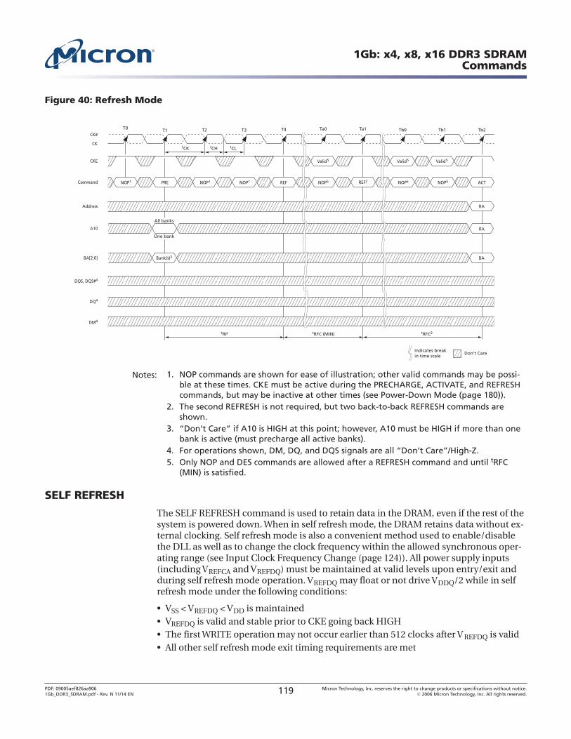
Figure 40: Refresh Mode
NOP1NOP1 NOP1PRE
RA
Bank(s)3 BA
REF NOP5 REF2 NOP5 ACTNOP5
One bank
All banks
tCK tCH tCL
RA
tRFC2tRP tRFC (MIN)
T0 T1 T2 T3 T4 Ta0 Tb0Ta1 Tb1 Tb2
Don’t CareIndicates breakin time scale
Valid5 Valid5 Valid5
CK
CK#
Command
CKE
Address
A10
BA[2:0]
DQ4
DM4
DQS, DQS#4
Notes: 1. NOP commands are shown for ease of illustration; other valid commands may be possi-ble at these times. CKE must be active during the PRECHARGE, ACTIVATE, and REFRESHcommands, but may be inactive at other times (see Power-Down Mode (page 180)).
2. The second REFRESH is not required, but two back-to-back REFRESH commands areshown.
3. “Don’t Care” if A10 is HIGH at this point; however, A10 must be HIGH if more than onebank is active (must precharge all active banks).
4. For operations shown, DM, DQ, and DQS signals are all “Don’t Care”/High-Z.5. Only NOP and DES commands are allowed after a REFRESH command and until tRFC
(MIN) is satisfied.
SELF REFRESH
The SELF REFRESH command is used to retain data in the DRAM, even if the rest of thesystem is powered down. When in self refresh mode, the DRAM retains data without ex-ternal clocking. Self refresh mode is also a convenient method used to enable/disablethe DLL as well as to change the clock frequency within the allowed synchronous oper-ating range (see Input Clock Frequency Change (page 124)). All power supply inputs(including VREFCA and VREFDQ) must be maintained at valid levels upon entry/exit andduring self refresh mode operation. VREFDQ may float or not drive VDDQ/2 while in selfrefresh mode under the following conditions:
• VSS < VREFDQ < VDD is maintained• VREFDQ is valid and stable prior to CKE going back HIGH• The first WRITE operation may not occur earlier than 512 clocks after V REFDQ is valid• All other self refresh mode exit timing requirements are met
1Gb: x4, x8, x16 DDR3 SDRAMCommands
PDF: 09005aef826aa9061Gb_DDR3_SDRAM.pdf - Rev. N 11/14 EN 119 Micron Technology, Inc. reserves the right to change products or specifications without notice.
© 2006 Micron Technology, Inc. All rights reserved.
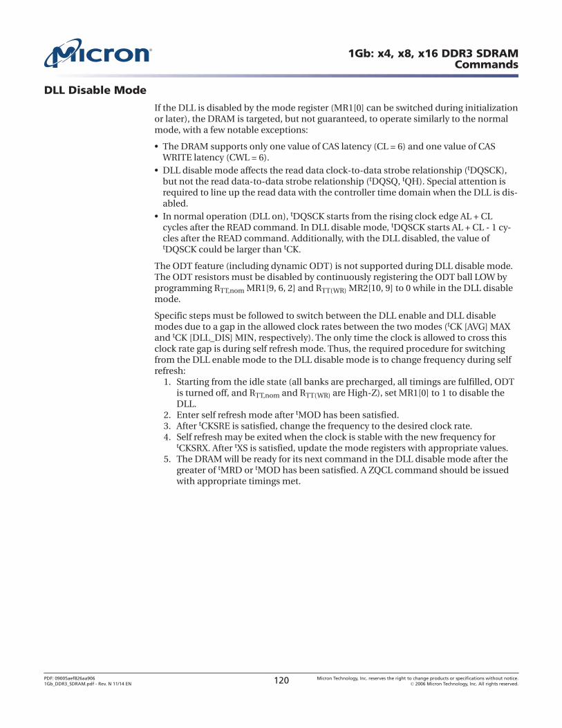
DLL Disable Mode
If the DLL is disabled by the mode register (MR1[0] can be switched during initializationor later), the DRAM is targeted, but not guaranteed, to operate similarly to the normalmode, with a few notable exceptions:
• The DRAM supports only one value of CAS latency (CL = 6) and one value of CASWRITE latency (CWL = 6).
• DLL disable mode affects the read data clock-to-data strobe relationship (tDQSCK),but not the read data-to-data strobe relationship (tDQSQ, tQH). Special attention isrequired to line up the read data with the controller time domain when the DLL is dis-abled.
• In normal operation (DLL on), tDQSCK starts from the rising clock edge AL + CLcycles after the READ command. In DLL disable mode, tDQSCK starts AL + CL - 1 cy-cles after the READ command. Additionally, with the DLL disabled, the value oftDQSCK could be larger than tCK.
The ODT feature (including dynamic ODT) is not supported during DLL disable mode.The ODT resistors must be disabled by continuously registering the ODT ball LOW byprogramming RTT,nom MR1[9, 6, 2] and RTT(WR) MR2[10, 9] to 0 while in the DLL disablemode.
Specific steps must be followed to switch between the DLL enable and DLL disablemodes due to a gap in the allowed clock rates between the two modes (tCK [AVG] MAXand tCK [DLL_DIS] MIN, respectively). The only time the clock is allowed to cross thisclock rate gap is during self refresh mode. Thus, the required procedure for switchingfrom the DLL enable mode to the DLL disable mode is to change frequency during selfrefresh:
1. Starting from the idle state (all banks are precharged, all timings are fulfilled, ODTis turned off, and RTT,nom and RTT(WR) are High-Z), set MR1[0] to 1 to disable theDLL.
2. Enter self refresh mode after tMOD has been satisfied.3. After tCKSRE is satisfied, change the frequency to the desired clock rate.4. Self refresh may be exited when the clock is stable with the new frequency for
tCKSRX. After tXS is satisfied, update the mode registers with appropriate values.5. The DRAM will be ready for its next command in the DLL disable mode after the
greater of tMRD or tMOD has been satisfied. A ZQCL command should be issuedwith appropriate timings met.
1Gb: x4, x8, x16 DDR3 SDRAMCommands
PDF: 09005aef826aa9061Gb_DDR3_SDRAM.pdf - Rev. N 11/14 EN 120 Micron Technology, Inc. reserves the right to change products or specifications without notice.
© 2006 Micron Technology, Inc. All rights reserved.
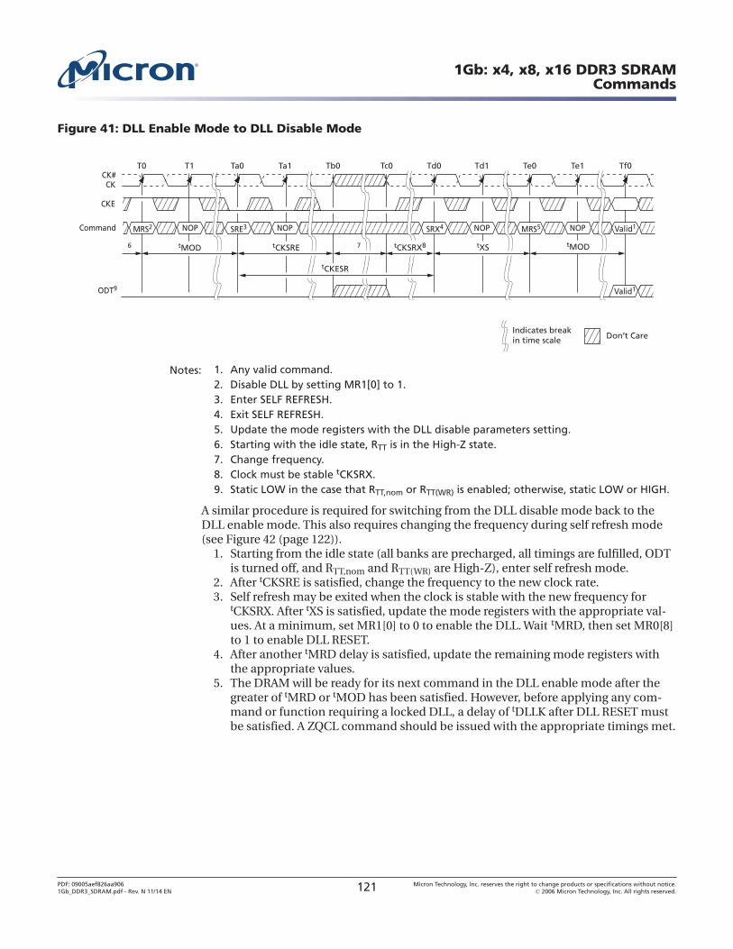
Figure 41: DLL Enable Mode to DLL Disable Mode
Command
T0 T1 Ta0 Ta1 Tb0 Tc0 Td0 Td1 Te0 Te1 Tf0
CKCK#
ODT9 Valid1
Don’t Care
Valid1
SRE3 NOPMRS2 NOP SRX4 MRS5 Valid1NOP NOP
Indicates breakin time scale
tMOD tCKSRE tMODtXS
tCKESR
CKE
tCKSRX876
Notes: 1. Any valid command.2. Disable DLL by setting MR1[0] to 1.3. Enter SELF REFRESH.4. Exit SELF REFRESH.5. Update the mode registers with the DLL disable parameters setting.6. Starting with the idle state, RTT is in the High-Z state.7. Change frequency.8. Clock must be stable tCKSRX.9. Static LOW in the case that RTT,nom or RTT(WR) is enabled; otherwise, static LOW or HIGH.
A similar procedure is required for switching from the DLL disable mode back to theDLL enable mode. This also requires changing the frequency during self refresh mode(see Figure 42 (page 122)).
1. Starting from the idle state (all banks are precharged, all timings are fulfilled, ODTis turned off, and RTT,nom and RTT(WR) are High-Z), enter self refresh mode.
2. After tCKSRE is satisfied, change the frequency to the new clock rate.3. Self refresh may be exited when the clock is stable with the new frequency for
tCKSRX. After tXS is satisfied, update the mode registers with the appropriate val-ues. At a minimum, set MR1[0] to 0 to enable the DLL. Wait tMRD, then set MR0[8]to 1 to enable DLL RESET.
4. After another tMRD delay is satisfied, update the remaining mode registers withthe appropriate values.
5. The DRAM will be ready for its next command in the DLL enable mode after thegreater of tMRD or tMOD has been satisfied. However, before applying any com-mand or function requiring a locked DLL, a delay of tDLLK after DLL RESET mustbe satisfied. A ZQCL command should be issued with the appropriate timings met.
1Gb: x4, x8, x16 DDR3 SDRAMCommands
PDF: 09005aef826aa9061Gb_DDR3_SDRAM.pdf - Rev. N 11/14 EN 121 Micron Technology, Inc. reserves the right to change products or specifications without notice.
© 2006 Micron Technology, Inc. All rights reserved.
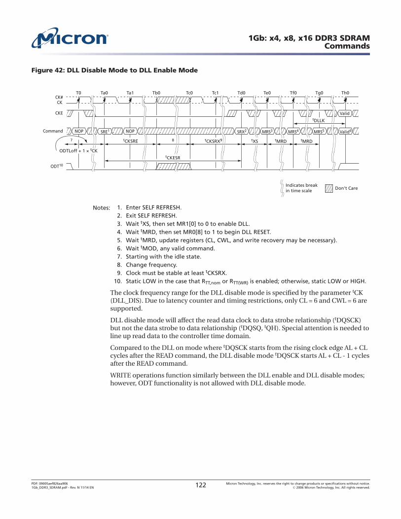
Figure 42: DLL Disable Mode to DLL Enable Mode
CKE
T0 Ta0 Ta1 Tb0 Tc0 Tc1 Td0 Te0 Tf0 Tg0
CKCK#
ODT10
SRE1 NOPCommand NOP SRX2 MRS3 MRS4 MRS5 Valid6
Valid
Don’t CareIndicates breakin time scale
tCKSRE tCKSRX987 tXS tMRD tMRD
tCKESR
ODTLoff + 1 × tCK
Th0
tDLLK
Notes: 1. Enter SELF REFRESH.2. Exit SELF REFRESH.3. Wait tXS, then set MR1[0] to 0 to enable DLL.4. Wait tMRD, then set MR0[8] to 1 to begin DLL RESET.5. Wait tMRD, update registers (CL, CWL, and write recovery may be necessary).6. Wait tMOD, any valid command.7. Starting with the idle state.8. Change frequency.9. Clock must be stable at least tCKSRX.
10. Static LOW in the case that RTT,nom or RTT(WR) is enabled; otherwise, static LOW or HIGH.
The clock frequency range for the DLL disable mode is specified by the parameter tCK(DLL_DIS). Due to latency counter and timing restrictions, only CL = 6 and CWL = 6 aresupported.
DLL disable mode will affect the read data clock to data strobe relationship (tDQSCK)but not the data strobe to data relationship (tDQSQ, tQH). Special attention is needed toline up read data to the controller time domain.
Compared to the DLL on mode where tDQSCK starts from the rising clock edge AL + CLcycles after the READ command, the DLL disable mode tDQSCK starts AL + CL - 1 cyclesafter the READ command.
WRITE operations function similarly between the DLL enable and DLL disable modes;however, ODT functionality is not allowed with DLL disable mode.
1Gb: x4, x8, x16 DDR3 SDRAMCommands
PDF: 09005aef826aa9061Gb_DDR3_SDRAM.pdf - Rev. N 11/14 EN 122 Micron Technology, Inc. reserves the right to change products or specifications without notice.
© 2006 Micron Technology, Inc. All rights reserved.
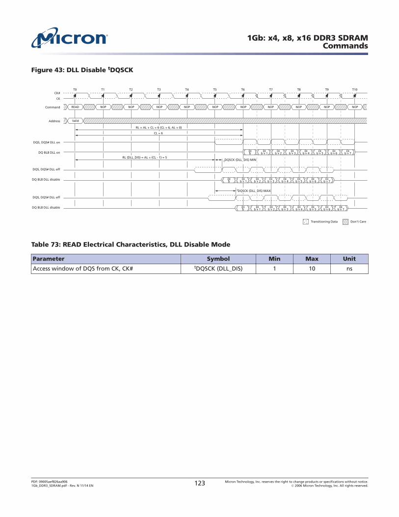
Figure 43: DLL Disable tDQSCK
T0 T1 T2 T3 T4 T5 T6 T7 T8 T9 T10
Don’t CareTransitioning Data
Valid
NOPREAD NOP NOP NOP NOP NOP NOP NOP NOP NOP
CK
CK#
Command
Address
DIb + 3
DIb + 2
DIb + 1
DIb
DIb + 7
DIb + 6
DIb + 5
DIb + 4
DQ BL8 DLL on
DQS, DQS# DLL on
DQ BL8 DLL disable
DQS, DQS# DLL off
DQ BL8 DLL disable
DQS, DQS# DLL off
RL = AL + CL = 6 (CL = 6, AL = 0)
CL = 6
DIb + 3
DIb + 2
DIb + 1
DIb
DIb + 7
DIb + 6
DIb + 5
DIb + 4
DIb + 3
DIb + 2
DIb + 1
DIb
DIb + 7
DIb + 6
DIb + 5
DIb + 4
tDQSCK (DLL_DIS) MIN
tDQSCK (DLL_DIS) MAX
RL (DLL_DIS) = AL + (CL - 1) = 5
Table 73: READ Electrical Characteristics, DLL Disable Mode
Parameter Symbol Min Max Unit
Access window of DQS from CK, CK# tDQSCK (DLL_DIS) 1 10 ns
1Gb: x4, x8, x16 DDR3 SDRAMCommands
PDF: 09005aef826aa9061Gb_DDR3_SDRAM.pdf - Rev. N 11/14 EN 123 Micron Technology, Inc. reserves the right to change products or specifications without notice.
© 2006 Micron Technology, Inc. All rights reserved.
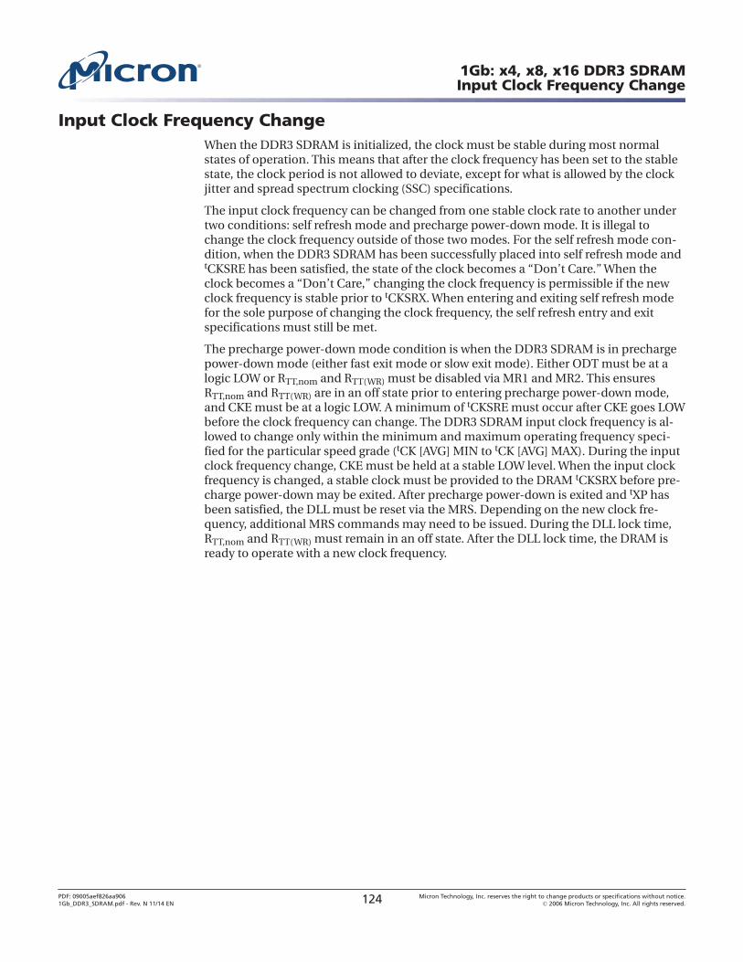
Input Clock Frequency ChangeWhen the DDR3 SDRAM is initialized, the clock must be stable during most normalstates of operation. This means that after the clock frequency has been set to the stablestate, the clock period is not allowed to deviate, except for what is allowed by the clockjitter and spread spectrum clocking (SSC) specifications.
The input clock frequency can be changed from one stable clock rate to another undertwo conditions: self refresh mode and precharge power-down mode. It is illegal tochange the clock frequency outside of those two modes. For the self refresh mode con-dition, when the DDR3 SDRAM has been successfully placed into self refresh mode andtCKSRE has been satisfied, the state of the clock becomes a “Don’t Care.” When theclock becomes a “Don’t Care,” changing the clock frequency is permissible if the newclock frequency is stable prior to tCKSRX. When entering and exiting self refresh modefor the sole purpose of changing the clock frequency, the self refresh entry and exitspecifications must still be met.
The precharge power-down mode condition is when the DDR3 SDRAM is in prechargepower-down mode (either fast exit mode or slow exit mode). Either ODT must be at alogic LOW or RTT,nom and RTT(WR) must be disabled via MR1 and MR2. This ensuresRTT,nom and RTT(WR) are in an off state prior to entering precharge power-down mode,and CKE must be at a logic LOW. A minimum of tCKSRE must occur after CKE goes LOWbefore the clock frequency can change. The DDR3 SDRAM input clock frequency is al-lowed to change only within the minimum and maximum operating frequency speci-fied for the particular speed grade (tCK [AVG] MIN to tCK [AVG] MAX). During the inputclock frequency change, CKE must be held at a stable LOW level. When the input clockfrequency is changed, a stable clock must be provided to the DRAM tCKSRX before pre-charge power-down may be exited. After precharge power-down is exited and tXP hasbeen satisfied, the DLL must be reset via the MRS. Depending on the new clock fre-quency, additional MRS commands may need to be issued. During the DLL lock time,RTT,nom and RTT(WR) must remain in an off state. After the DLL lock time, the DRAM isready to operate with a new clock frequency.
1Gb: x4, x8, x16 DDR3 SDRAMInput Clock Frequency Change
PDF: 09005aef826aa9061Gb_DDR3_SDRAM.pdf - Rev. N 11/14 EN 124 Micron Technology, Inc. reserves the right to change products or specifications without notice.
© 2006 Micron Technology, Inc. All rights reserved.
Figure 44: Change Frequency During Precharge Power-Down
CK
CK#
Command NOPNOPNOP
Address
CKE
DQ
DM
DQS, DQS#
NOP
tCK
Enter prechargepower-down mode
Exit prechargepower-down mode
T0 T1 Ta0 Tc0Tb0T2
Don’t Care
tCKE
tXP
MRS
DLL RESET
Valid
Valid
NOP
tCH
tIH tIS
tCL
Tc1 Td0 Te1Td1
tCKSRE
tCHbtCLb
tCKb
tCHbtCLb
tCKb
tCHbtCLb
tCKb
tCPDED
ODT
NOP
Te0
Previous clock frequency New clock frequency
Frequencychange
Indicates breakin time scale
tIH tIS
tIH
tIS
tDLLK
tAOFPD/tAOF
tCKSRX
High-Z
High-Z
Notes: 1. Applicable for both SLOW-EXIT and FAST-EXIT precharge power-down modes.2. tAOFPD and tAOF must be satisfied and outputs High-Z prior to T1 (see On-Die Termina-
tion (ODT) (page 190) for exact requirements).3. If the RTT,nom feature was enabled in the mode register prior to entering precharge
power-down mode, the ODT signal must be continuously registered LOW, ensuring RTTis in an off state. If the RTT,nom feature was disabled in the mode register prior to enter-ing precharge power-down mode, RTT will remain in the off state. The ODT signal canbe registered LOW or HIGH in this case.
1Gb: x4, x8, x16 DDR3 SDRAMInput Clock Frequency Change
PDF: 09005aef826aa9061Gb_DDR3_SDRAM.pdf - Rev. N 11/14 EN 125 Micron Technology, Inc. reserves the right to change products or specifications without notice.
© 2006 Micron Technology, Inc. All rights reserved.
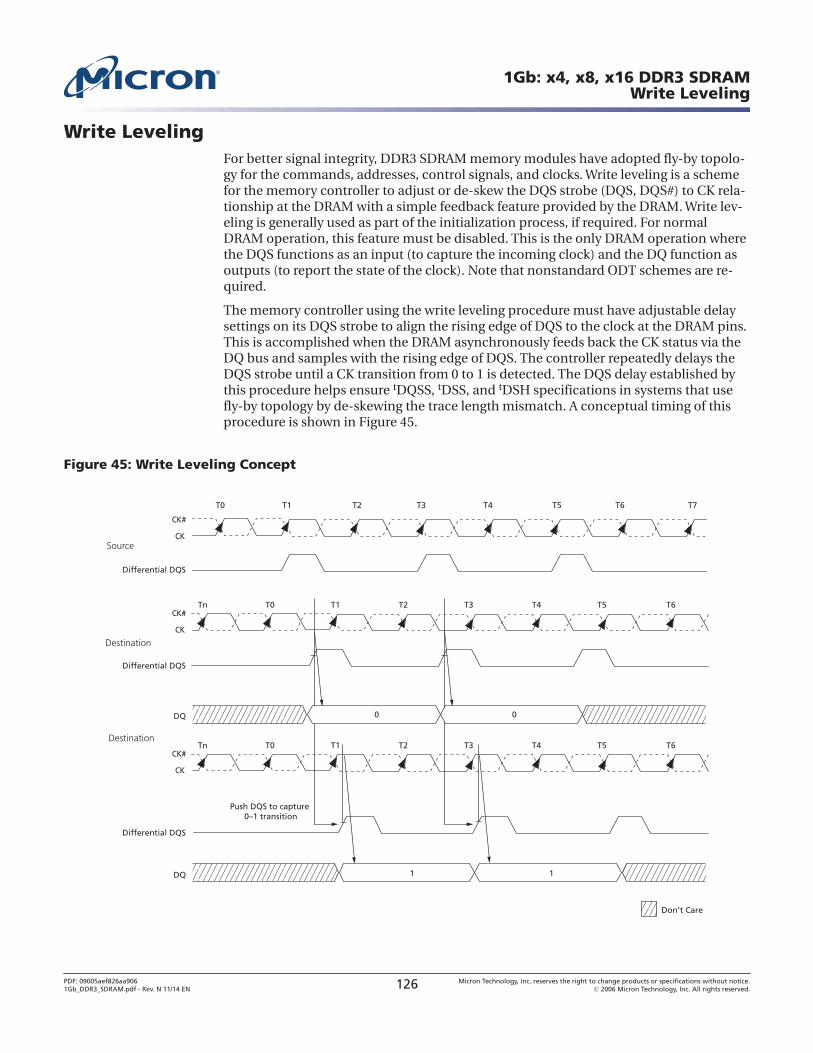
Write LevelingFor better signal integrity, DDR3 SDRAM memory modules have adopted fly-by topolo-gy for the commands, addresses, control signals, and clocks. Write leveling is a schemefor the memory controller to adjust or de-skew the DQS strobe (DQS, DQS#) to CK rela-tionship at the DRAM with a simple feedback feature provided by the DRAM. Write lev-eling is generally used as part of the initialization process, if required. For normalDRAM operation, this feature must be disabled. This is the only DRAM operation wherethe DQS functions as an input (to capture the incoming clock) and the DQ function asoutputs (to report the state of the clock). Note that nonstandard ODT schemes are re-quired.
The memory controller using the write leveling procedure must have adjustable delaysettings on its DQS strobe to align the rising edge of DQS to the clock at the DRAM pins.This is accomplished when the DRAM asynchronously feeds back the CK status via theDQ bus and samples with the rising edge of DQS. The controller repeatedly delays theDQS strobe until a CK transition from 0 to 1 is detected. The DQS delay established bythis procedure helps ensure tDQSS, tDSS, and tDSH specifications in systems that usefly-by topology by de-skewing the trace length mismatch. A conceptual timing of thisprocedure is shown in Figure 45.
Figure 45: Write Leveling Concept
CK
CK#
Source
Differential DQS
Differential DQS
Differential DQS
DQ
DQ
CK
CK#
Destination
Destination
Push DQS to capture 0–1 transition
T0 T1 T2 T3 T4 T5 T6 T7
T0 T1 T2 T3 T4 T5 T6Tn
CK
CK#T0 T1 T2 T3 T4 T5 T6Tn
Don’t Care
1 1
00
1Gb: x4, x8, x16 DDR3 SDRAMWrite Leveling
PDF: 09005aef826aa9061Gb_DDR3_SDRAM.pdf - Rev. N 11/14 EN 126 Micron Technology, Inc. reserves the right to change products or specifications without notice.
© 2006 Micron Technology, Inc. All rights reserved.
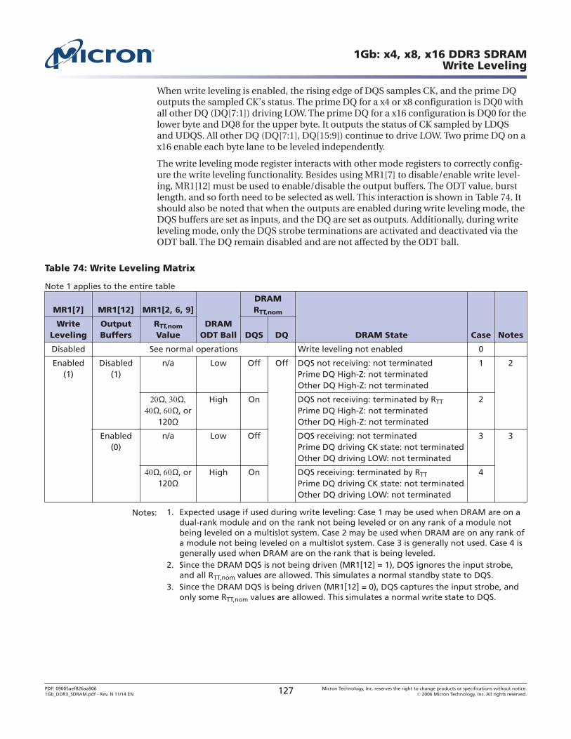
When write leveling is enabled, the rising edge of DQS samples CK, and the prime DQoutputs the sampled CK’s status. The prime DQ for a x4 or x8 configuration is DQ0 withall other DQ (DQ[7:1]) driving LOW. The prime DQ for a x16 configuration is DQ0 for thelower byte and DQ8 for the upper byte. It outputs the status of CK sampled by LDQSand UDQS. All other DQ (DQ[7:1], DQ[15:9]) continue to drive LOW. Two prime DQ on ax16 enable each byte lane to be leveled independently.
The write leveling mode register interacts with other mode registers to correctly config-ure the write leveling functionality. Besides using MR1[7] to disable/enable write level-ing, MR1[12] must be used to enable/disable the output buffers. The ODT value, burstlength, and so forth need to be selected as well. This interaction is shown in Table 74. Itshould also be noted that when the outputs are enabled during write leveling mode, theDQS buffers are set as inputs, and the DQ are set as outputs. Additionally, during writeleveling mode, only the DQS strobe terminations are activated and deactivated via theODT ball. The DQ remain disabled and are not affected by the ODT ball.
Table 74: Write Leveling Matrix
Note 1 applies to the entire table
MR1[7] MR1[12] MR1[2, 6, 9]
DRAMODT Ball
DRAMRTT,nom
DRAM State Case NotesWrite
LevelingOutputBuffers
RTT,nom
Value DQS DQ
Disabled See normal operations Write leveling not enabled 0
Enabled(1)
Disabled(1)
n/a Low Off Off DQS not receiving: not terminatedPrime DQ High-Z: not terminatedOther DQ High-Z: not terminated
1 2
ΩΩΩΩ, or
120Ω
High On DQS not receiving: terminated by RTT
Prime DQ High-Z: not terminatedOther DQ High-Z: not terminated
2
Enabled(0)
n/a Low Off DQS receiving: not terminatedPrime DQ driving CK state: not terminatedOther DQ driving LOW: not terminated
3 3
ΩΩ, or120Ω
High On DQS receiving: terminated by RTT
Prime DQ driving CK state: not terminatedOther DQ driving LOW: not terminated
4
Notes: 1. Expected usage if used during write leveling: Case 1 may be used when DRAM are on adual-rank module and on the rank not being leveled or on any rank of a module notbeing leveled on a multislot system. Case 2 may be used when DRAM are on any rank ofa module not being leveled on a multislot system. Case 3 is generally not used. Case 4 isgenerally used when DRAM are on the rank that is being leveled.
2. Since the DRAM DQS is not being driven (MR1[12] = 1), DQS ignores the input strobe,and all RTT,nom values are allowed. This simulates a normal standby state to DQS.
3. Since the DRAM DQS is being driven (MR1[12] = 0), DQS captures the input strobe, andonly some RTT,nom values are allowed. This simulates a normal write state to DQS.
1Gb: x4, x8, x16 DDR3 SDRAMWrite Leveling
PDF: 09005aef826aa9061Gb_DDR3_SDRAM.pdf - Rev. N 11/14 EN 127 Micron Technology, Inc. reserves the right to change products or specifications without notice.
© 2006 Micron Technology, Inc. All rights reserved.
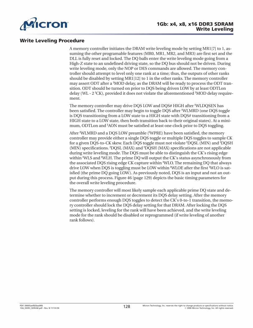
Write Leveling Procedure
A memory controller initiates the DRAM write leveling mode by setting MR1[7] to 1, as-suming the other programable features (MR0, MR1, MR2, and MR3) are first set and theDLL is fully reset and locked. The DQ balls enter the write leveling mode going from aHigh-Z state to an undefined driving state, so the DQ bus should not be driven. Duringwrite leveling mode, only the NOP or DES commands are allowed. The memory con-troller should attempt to level only one rank at a time; thus, the outputs of other ranksshould be disabled by setting MR1[12] to 1 in the other ranks. The memory controllermay assert ODT after a tMOD delay, as the DRAM will be ready to process the ODT tran-sition. ODT should be turned on prior to DQS being driven LOW by at least ODTLondelay (WL - 2 tCK), provided it does not violate the aforementioned tMOD delay require-ment.
The memory controller may drive DQS LOW and DQS# HIGH after tWLDQSEN hasbeen satisfied. The controller may begin to toggle DQS after tWLMRD (one DQS toggleis DQS transitioning from a LOW state to a HIGH state with DQS# transitioning from aHIGH state to a LOW state, then both transition back to their original states). At a mini-mum, ODTLon and tAON must be satisfied at least one clock prior to DQS toggling.
After tWLMRD and a DQS LOW preamble (tWPRE) have been satisfied, the memorycontroller may provide either a single DQS toggle or multiple DQS toggles to sample CKfor a given DQS-to-CK skew. Each DQS toggle must not violate tDQSL (MIN) and tDQSH(MIN) specifications. tDQSL (MAX) and tDQSH (MAX) specifications are not applicableduring write leveling mode. The DQS must be able to distinguish the CK’s rising edgewithin tWLS and tWLH. The prime DQ will output the CK’s status asynchronously fromthe associated DQS rising edge CK capture within tWLO. The remaining DQ that alwaysdrive LOW when DQS is toggling must be LOW within tWLOE after the first tWLO is sat-isfied (the prime DQ going LOW). As previously noted, DQS is an input and not an out-put during this process. Figure 46 (page 129) depicts the basic timing parameters forthe overall write leveling procedure.
The memory controller will most likely sample each applicable prime DQ state and de-termine whether to increment or decrement its DQS delay setting. After the memorycontroller performs enough DQS toggles to detect the CK’s 0-to-1 transition, the memo-ry controller should lock the DQS delay setting for that DRAM. After locking the DQSsetting is locked, leveling for the rank will have been achieved, and the write levelingmode for the rank should be disabled or reprogrammed (if write leveling of anotherrank follows).
1Gb: x4, x8, x16 DDR3 SDRAMWrite Leveling
PDF: 09005aef826aa9061Gb_DDR3_SDRAM.pdf - Rev. N 11/14 EN 128 Micron Technology, Inc. reserves the right to change products or specifications without notice.
© 2006 Micron Technology, Inc. All rights reserved.

Figure 46: Write Leveling Sequence
CKCK#
Command
T1 T2
Early remaining DQ
Late remaining DQ
tWLOE
NOP2 NOPMRS1 NOP NOP NOP NOP NOP NOP NOP NOP NOP
tWLStWLH
Don’t CareUndefined Driving ModeIndicates breakin time scale
Prime DQ5
Differential DQS4
ODT
tMOD
tDQSL3 tDQSL3tDQSH3 tDQSH3
tWLOtWLMRD
tWLDQSEN
tWLO
tWLO
tWLO
Notes: 1. MRS: Load MR1 to enter write leveling mode.2. NOP: NOP or DES.3. DQS, DQS# needs to fulfill minimum pulse width requirements tDQSH (MIN) and tDQSL
(MIN) as defined for regular writes. The maximum pulse width is system-dependent.4. Differential DQS is the differential data strobe (DQS, DQS#). Timing reference points are
the zero crossings. The solid line represents DQS; the dotted line represents DQS#.5. DRAM drives leveling feedback on a prime DQ (DQ0 for x4 and x8). The remaining DQ
are driven LOW and remain in this state throughout the leveling procedure.
1Gb: x4, x8, x16 DDR3 SDRAMWrite Leveling
PDF: 09005aef826aa9061Gb_DDR3_SDRAM.pdf - Rev. N 11/14 EN 129 Micron Technology, Inc. reserves the right to change products or specifications without notice.
© 2006 Micron Technology, Inc. All rights reserved.
Write Leveling Mode Exit Procedure
After the DRAM are leveled, they must exit from write leveling mode before the normalmode can be used. Figure 47 depicts a general procedure for exiting write levelingmode. After the last rising DQS (capturing a 1 at T0), the memory controller should stopdriving the DQS signals after tWLO (MAX) delay plus enough delay to enable the memo-ry controller to capture the applicable prime DQ state (at ~Tb0). The DQ balls becomeundefined when DQS no longer remains LOW, and they remain undefined until tMODafter the MRS command (at Te1).
The ODT input should be de-asserted LOW such that ODTLoff (MIN) expires after theDQS is no longer driving LOW. When ODT LOW satisfies tIS, ODT must be kept LOW (at~Tb0) until the DRAM is ready for either another rank to be leveled or until the normalmode can be used. After DQS termination is switched off, write level mode should bedisabled via the MRS command (at Tc2). After tMOD is satisfied (at Te1), any valid com-mand may be registered by the DRAM. Some MRS commands may be issued after tMRD(at Td1).
Figure 47: Write Leveling Exit Procedure
NOP
CK
T0 T1 T2 Ta0 Tb0 Tc0 Tc1 Tc2 Td0 Td1 Te0 Te1CK#
Command
ODT
RTT(DQ)
NOPNOP NOP NOP NOP NOP MRS NOP NOP
Address MR1
Valid Valid
Valid Valid
Don’t CareTransitioning
RTT DQS, RTT DQS# RTT,nom
Undefined Driving Mode
tAOF (MAX)
tMRD
Indicates breakin time scale
DQS, DQS#
CK = 1DQ
tIS
tAOF (MIN)
tMOD
tWLO + tWLOE
ODTLoff
Note: 1. The DQ result, = 1, between Ta0 and Tc0, is a result of the DQS, DQS# signals capturingCK HIGH just after the T0 state.
1Gb: x4, x8, x16 DDR3 SDRAMWrite Leveling
PDF: 09005aef826aa9061Gb_DDR3_SDRAM.pdf - Rev. N 11/14 EN 130 Micron Technology, Inc. reserves the right to change products or specifications without notice.
© 2006 Micron Technology, Inc. All rights reserved.
InitializationThe following sequence is required for power-up and initialization, as shown in Fig-ure 48 (page 132):
1. Apply power. RESET# is recommended to be below 0.2 × VDDQ during power rampto ensure the outputs remain disabled (High-Z) and ODT off (RTT is also High-Z).All other inputs, including ODT, may be undefined.
During power-up, either of the following conditions may exist and must be met:
• Condition A:– VDD and VDDQ are driven from a single-power converter output and are
ramped with a maximum delta voltage between them of ΔV ≤ 300mV. Slope re-versal of any power supply signal is allowed. The voltage levels on all balls oth-er than VDD, VDDQ, VSS, VSSQ must be less than or equal to VDDQ and VDD onone side, and must be greater than or equal to VSSQ and VSS on the other side.
– Both VDD and VDDQ power supplies ramp to VDD,min and VDDQ,min withintVDDPR = 200ms.
– VREFDQ tracks VDD × 0.5, VREFCA tracks VDD × 0.5.– VTT is limited to 0.95V when the power ramp is complete and is not applied
directly to the device; however, tVTD should be greater than or equal to 0 toavoid device latchup.
• Condition B:– VDD may be applied before or at the same time as VDDQ.– VDDQ may be applied before or at the same time as VTT, VREFDQ, and VREFCA.– No slope reversals are allowed in the power supply ramp for this condition.
2. Until stable power, maintain RESET# LOW to ensure the outputs remain disabled(High-Z). After the power is stable, RESET# must be LOW for at least 200μs to be-gin the initialization process. ODT will remain in the High-Z state while RESET# isLOW and until CKE is registered HIGH.
3. CKE must be LOW 10ns prior to RESET# transitioning HIGH.4. After RESET# transitions HIGH, wait 500μs (minus one clock) with CKE LOW.5. After the CKE LOW time, CKE may be brought HIGH (synchronously) and only
NOP or DES commands may be issued. The clock must be present and valid for atleast 10ns (and a minimum of five clocks) and ODT must be driven LOW at leasttIS prior to CKE being registered HIGH. When CKE is registered HIGH, it must becontinuously registered HIGH until the full initialization process is complete.
6. After CKE is registered HIGH and after tXPR has been satisfied, MRS commandsmay be issued. Issue an MRS (LOAD MODE) command to MR2 with the applicablesettings (provide LOW to BA2 and BA0 and HIGH to BA1).
7. Issue an MRS command to MR3 with the applicable settings.8. Issue an MRS command to MR1 with the applicable settings, including enabling
the DLL and configuring ODT.9. Issue an MRS command to MR0 with the applicable settings, including a DLL RE-
SET command. tDLLK (512) cycles of clock input are required to lock the DLL.10. Issue a ZQCL command to calibrate RTT and RON values for the process voltage
temperature (PVT). Prior to normal operation, tZQinit must be satisfied.11. When tDLLK and tZQinit have been satisfied, the DDR3 SDRAM will be ready for
normal operation.
1Gb: x4, x8, x16 DDR3 SDRAMInitialization
PDF: 09005aef826aa9061Gb_DDR3_SDRAM.pdf - Rev. N 11/14 EN 131 Micron Technology, Inc. reserves the right to change products or specifications without notice.
© 2006 Micron Technology, Inc. All rights reserved.
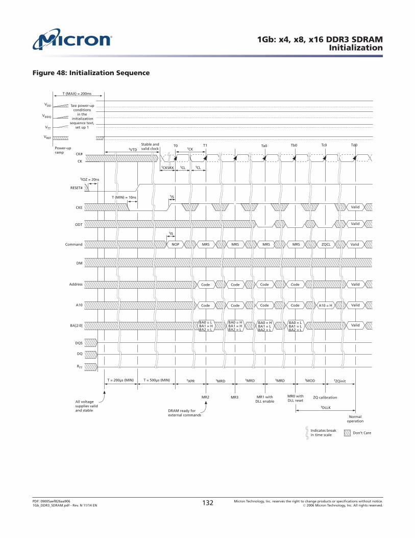
Figure 48: Initialization Sequence
CKE
RTT
BA[2:0]
All voltagesupplies validand stable
T = 200μs (MIN)
DM
DQS
Address
A10
CK
CK#
tCL
Command NOP
T0 Ta0
Don’t Care
tCL
tIS
tCK
ODT
DQ
Tb0
tDLLK
MR1 withDLL enable
MR0 withDLL reset
tMRD tMOD
MRSMRS
BA0 = HBA1 = LBA2 = L
BA0 = LBA1 = LBA2 = L
Code Code
Code Code
Valid
Valid
Valid
Valid
Normaloperation
MR2 MR3
tMRD tMRD
MRSMRS
BA0 = LBA1 = HBA2 = L
BA0 = HBA1 = HBA2 = L
Code Code
Code Code
Tc0 Td0
VTT
VREF
VDDQ
VDD
RESET#
T = 500μs (MIN)
tCKSRX
Stable andvalid clock
Valid
Power-upramp
T (MAX) = 200ms
DRAM ready for external commands
T1
tZQinit
ZQ calibration
A10 = H
ZQCL
tIS
See power-upconditions
in the initialization
sequence text, set up 1
tXPR
Valid
tIOZ = 20ns
Indicates breakin time scale
T (MIN) = 10ns
tVTD
1Gb: x4, x8, x16 DDR3 SDRAMInitialization
PDF: 09005aef826aa9061Gb_DDR3_SDRAM.pdf - Rev. N 11/14 EN 132 Micron Technology, Inc. reserves the right to change products or specifications without notice.
© 2006 Micron Technology, Inc. All rights reserved.
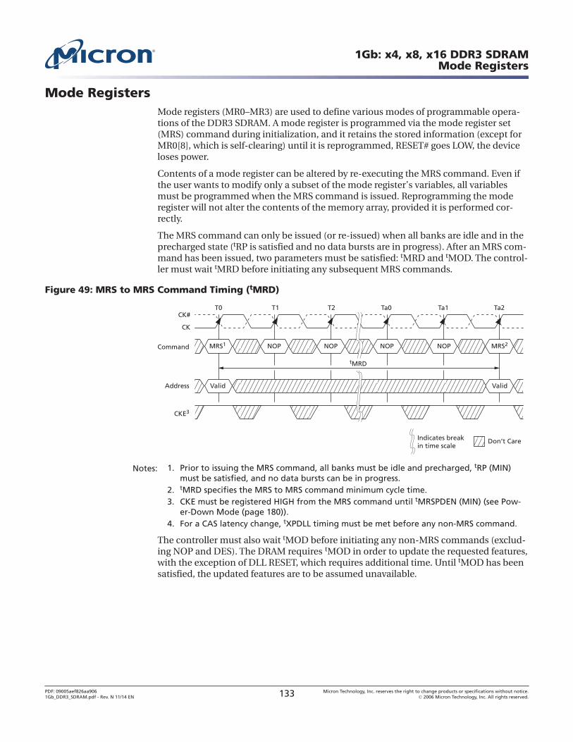
Mode RegistersMode registers (MR0–MR3) are used to define various modes of programmable opera-tions of the DDR3 SDRAM. A mode register is programmed via the mode register set(MRS) command during initialization, and it retains the stored information (except forMR0[8], which is self-clearing) until it is reprogrammed, RESET# goes LOW, the deviceloses power.
Contents of a mode register can be altered by re-executing the MRS command. Even ifthe user wants to modify only a subset of the mode register’s variables, all variablesmust be programmed when the MRS command is issued. Reprogramming the moderegister will not alter the contents of the memory array, provided it is performed cor-rectly.
The MRS command can only be issued (or re-issued) when all banks are idle and in theprecharged state (tRP is satisfied and no data bursts are in progress). After an MRS com-mand has been issued, two parameters must be satisfied: tMRD and tMOD. The control-ler must wait tMRD before initiating any subsequent MRS commands.
Figure 49: MRS to MRS Command Timing (tMRD)
Valid Valid
MRS1 MRS2NOP NOP NOP NOP
T0 T1 T2 Ta0 Ta1 Ta2CK#
CK
Command
Address
CKE3
Don’t CareIndicates breakin time scale
tMRD
Notes: 1. Prior to issuing the MRS command, all banks must be idle and precharged, tRP (MIN)must be satisfied, and no data bursts can be in progress.
2. tMRD specifies the MRS to MRS command minimum cycle time.3. CKE must be registered HIGH from the MRS command until tMRSPDEN (MIN) (see Pow-
er-Down Mode (page 180)).4. For a CAS latency change, tXPDLL timing must be met before any non-MRS command.
The controller must also wait tMOD before initiating any non-MRS commands (exclud-ing NOP and DES). The DRAM requires tMOD in order to update the requested features,with the exception of DLL RESET, which requires additional time. Until tMOD has beensatisfied, the updated features are to be assumed unavailable.
1Gb: x4, x8, x16 DDR3 SDRAMMode Registers
PDF: 09005aef826aa9061Gb_DDR3_SDRAM.pdf - Rev. N 11/14 EN 133 Micron Technology, Inc. reserves the right to change products or specifications without notice.
© 2006 Micron Technology, Inc. All rights reserved.
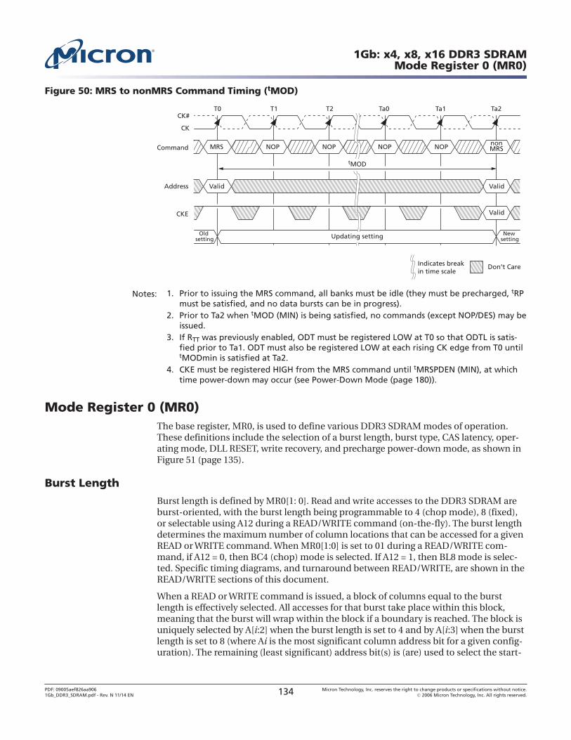
Figure 50: MRS to nonMRS Command Timing (tMOD)
Valid Valid
MRS nonMRSNOP NOP NOP NOP
T0 T1 T2 Ta0 Ta1 Ta2CK#
CK
Command
Address
CKE Valid
Old setting
New setting
Indicates breakin time scale
tMOD
Updating setting
Don’t Care
Notes: 1. Prior to issuing the MRS command, all banks must be idle (they must be precharged, tRPmust be satisfied, and no data bursts can be in progress).
2. Prior to Ta2 when tMOD (MIN) is being satisfied, no commands (except NOP/DES) may beissued.
3. If RTT was previously enabled, ODT must be registered LOW at T0 so that ODTL is satis-fied prior to Ta1. ODT must also be registered LOW at each rising CK edge from T0 untiltMODmin is satisfied at Ta2.
4. CKE must be registered HIGH from the MRS command until tMRSPDEN (MIN), at whichtime power-down may occur (see Power-Down Mode (page 180)).
Mode Register 0 (MR0)The base register, MR0, is used to define various DDR3 SDRAM modes of operation.These definitions include the selection of a burst length, burst type, CAS latency, oper-ating mode, DLL RESET, write recovery, and precharge power-down mode, as shown inFigure 51 (page 135).
Burst Length
Burst length is defined by MR0[1: 0]. Read and write accesses to the DDR3 SDRAM areburst-oriented, with the burst length being programmable to 4 (chop mode), 8 (fixed),or selectable using A12 during a READ/WRITE command (on-the-fly). The burst lengthdetermines the maximum number of column locations that can be accessed for a givenREAD or WRITE command. When MR0[1:0] is set to 01 during a READ/WRITE com-mand, if A12 = 0, then BC4 (chop) mode is selected. If A12 = 1, then BL8 mode is selec-ted. Specific timing diagrams, and turnaround between READ/WRITE, are shown in theREAD/WRITE sections of this document.
When a READ or WRITE command is issued, a block of columns equal to the burstlength is effectively selected. All accesses for that burst take place within this block,meaning that the burst will wrap within the block if a boundary is reached. The block isuniquely selected by A[i:2] when the burst length is set to 4 and by A[i:3] when the burstlength is set to 8 (where Ai is the most significant column address bit for a given config-uration). The remaining (least significant) address bit(s) is (are) used to select the start-
1Gb: x4, x8, x16 DDR3 SDRAMMode Register 0 (MR0)
PDF: 09005aef826aa9061Gb_DDR3_SDRAM.pdf - Rev. N 11/14 EN 134 Micron Technology, Inc. reserves the right to change products or specifications without notice.
© 2006 Micron Technology, Inc. All rights reserved.
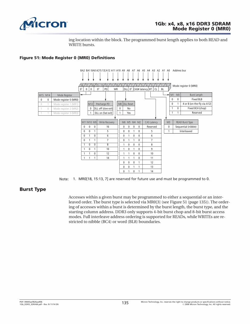
ing location within the block. The programmed burst length applies to both READ andWRITE bursts.
Figure 51: Mode Register 0 (MR0) Definitions
BLCAS# latency CLBTPD
A9 A7 A6 A5 A4 A3A8 A2 A1 A0
Mode register 0 (MR0)
Address bus
9 7 6 5 4 38 2 1 0
A10A12 A11BA0BA1
10111215 - 13
M3
0
1
READ Burst Type
Sequential (nibble)
Interleaved
CAS Latency
Reserved
5
6
7
8
9
10
11
12
13
14
M2
0
0
0
0
0
0
0
0
1
1
1
M4
0
1
0
1
0
1
0
1
0
1
0
M5
0
0
1
1
0
0
1
1
0
0
1
M6
0
0
0
0
1
1
1
1
0
0
0
17DLL
Write Recovery
16
5
6
7
8
10
12
14
WR00
M12
0
1
Precharge PD
DLL off (slow exit)
DLL on (fast exit)
BA2
1801
Burst Length
Fixed BL8
4 or 8 (on-the-fly via A12)
Fixed BC4 (chop)
Reserved
M0
0
1
0
1
M1
0
0
1
1
M9
0
1
0
1
0
1
0
1
M10
0
0
1
1
0
0
1
1
M11
0
0
0
0
1
1
1
1
M14
0
1
0
1
M15
0
0
1
1
Mode Register
Mode register 0 (MR0)
Mode register 1 (MR1)
Mode register 2 (MR2)
Mode register 3 (MR3)
A[15:13]
1601 01
M8
0
1
DLL Reset
No
Yes
Note: 1. MR0[18, 15:13, 7] are reserved for future use and must be programmed to 0.
Burst Type
Accesses within a given burst may be programmed to either a sequential or an inter-leaved order. The burst type is selected via MR0[3] (see Figure 51 (page 135)). The order-ing of accesses within a burst is determined by the burst length, the burst type, and thestarting column address. DDR3 only supports 4-bit burst chop and 8-bit burst accessmodes. Full interleave address ordering is supported for READs, while WRITEs are re-stricted to nibble (BC4) or word (BL8) boundaries.
1Gb: x4, x8, x16 DDR3 SDRAMMode Register 0 (MR0)
PDF: 09005aef826aa9061Gb_DDR3_SDRAM.pdf - Rev. N 11/14 EN 135 Micron Technology, Inc. reserves the right to change products or specifications without notice.
© 2006 Micron Technology, Inc. All rights reserved.
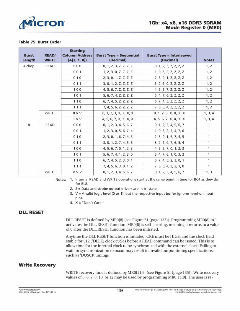
Table 75: Burst Order
BurstLength
READ/WRITE
StartingColumn Address
(A[2, 1, 0])Burst Type = Sequential
(Decimal)Burst Type = Interleaved
(Decimal) Notes
4 chop READ 0 0 0 0, 1, 2, 3, Z, Z, Z, Z 0, 1, 2, 3, Z, Z, Z, Z 1, 2
0 0 1 1, 2, 3, 0, Z, Z, Z, Z 1, 0, 3, 2, Z, Z, Z, Z 1, 2
0 1 0 2, 3, 0, 1, Z, Z, Z, Z 2, 3, 0, 1, Z, Z, Z, Z 1, 2
0 1 1 3, 0, 1, 2, Z, Z, Z, Z 3, 2, 1, 0, Z, Z, Z, Z 1, 2
1 0 0 4, 5, 6, 7, Z, Z, Z, Z 4, 5, 6, 7, Z, Z, Z, Z 1, 2
1 0 1 5, 6, 7, 4, Z, Z, Z, Z 5, 4, 7, 6, Z, Z, Z, Z 1, 2
1 1 0 6, 7, 4, 5, Z, Z, Z, Z 6, 7, 4, 5, Z, Z, Z, Z 1, 2
1 1 1 7, 4, 5, 6, Z, Z, Z, Z 7, 6, 5, 4, Z, Z, Z, Z 1, 2
WRITE 0 V V 0, 1, 2, 3, X, X, X, X 0, 1, 2, 3, X, X, X, X 1, 3, 4
1 V V 4, 5, 6, 7, X, X, X, X 4, 5, 6, 7, X, X, X, X 1, 3, 4
8 READ 0 0 0 0, 1, 2, 3, 4, 5, 6, 7 0, 1, 2, 3, 4, 5, 6, 7 1
0 0 1 1, 2, 3, 0, 5, 6, 7, 4 1, 0, 3, 2, 5, 4, 7, 6 1
0 1 0 2, 3, 0, 1, 6, 7, 4, 5 2, 3, 0, 1, 6, 7, 4, 5 1
0 1 1 3, 0, 1, 2, 7, 4, 5, 6 3, 2, 1, 0, 7, 6, 5, 4 1
1 0 0 4, 5, 6, 7, 0, 1, 2, 3 4, 5, 6, 7, 0, 1, 2, 3 1
1 0 1 5, 6, 7, 4, 1, 2, 3, 0 5, 4, 7, 6, 1, 0, 3, 2 1
1 1 0 6, 7, 4, 5, 2, 3, 0, 1 6, 7, 4, 5, 2, 3, 0, 1 1
1 1 1 7, 4, 5, 6, 3, 0, 1, 2 7, 6, 5, 4, 3, 2, 1, 0 1
WRITE V V V 0, 1, 2, 3, 4, 5, 6, 7 0, 1, 2, 3, 4, 5, 6, 7 1, 3
Notes: 1. Internal READ and WRITE operations start at the same point in time for BC4 as they dofor BL8.
2. Z = Data and strobe output drivers are in tri-state.3. V = A valid logic level (0 or 1), but the respective input buffer ignores level-on input
pins.4. X = “Don’t Care.”
DLL RESET
DLL RESET is defined by MR0[8] (see Figure 51 (page 135)). Programming MR0[8] to 1activates the DLL RESET function. MR0[8] is self-clearing, meaning it returns to a valueof 0 after the DLL RESET function has been initiated.
Anytime the DLL RESET function is initiated, CKE must be HIGH and the clock heldstable for 512 (tDLLK) clock cycles before a READ command can be issued. This is toallow time for the internal clock to be synchronized with the external clock. Failing towait for synchronization to occur may result in invalid output timing specifications,such as tDQSCK timings.
Write Recovery
WRITE recovery time is defined by MR0[11:9] (see Figure 51 (page 135)). Write recoveryvalues of 5, 6, 7, 8, 10, or 12 may be used by programming MR0[11:9]. The user is re-
1Gb: x4, x8, x16 DDR3 SDRAMMode Register 0 (MR0)
PDF: 09005aef826aa9061Gb_DDR3_SDRAM.pdf - Rev. N 11/14 EN 136 Micron Technology, Inc. reserves the right to change products or specifications without notice.
© 2006 Micron Technology, Inc. All rights reserved.
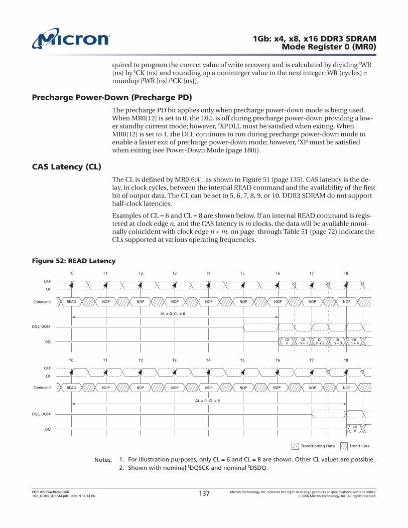
quired to program the correct value of write recovery and is calculated by dividing tWR(ns) by tCK (ns) and rounding up a noninteger value to the next integer: WR (cycles) =roundup (tWR [ns]/tCK [ns]).
Precharge Power-Down (Precharge PD)
The precharge PD bit applies only when precharge power-down mode is being used.When MR0[12] is set to 0, the DLL is off during precharge power-down providing a low-er standby current mode; however, tXPDLL must be satisfied when exiting. WhenMR0[12] is set to 1, the DLL continues to run during precharge power-down mode toenable a faster exit of precharge power-down mode; however, tXP must be satisfiedwhen exiting (see Power-Down Mode (page 180)).
CAS Latency (CL)
The CL is defined by MR0[6:4], as shown in Figure 51 (page 135). CAS latency is the de-lay, in clock cycles, between the internal READ command and the availability of the firstbit of output data. The CL can be set to 5, 6, 7, 8, 9, or 10. DDR3 SDRAM do not supporthalf-clock latencies.
Examples of CL = 6 and CL = 8 are shown below. If an internal READ command is regis-tered at clock edge n, and the CAS latency is m clocks, the data will be available nomi-nally coincident with clock edge n + m. on page through Table 51 (page 72) indicate theCLs supported at various operating frequencies.
Figure 52: READ Latency
READ NOP NOP NOP NOP NOP NOPNOP
CK
CK#
Command
DQ
DQS, DQS#
DQS, DQS#
T0 T1 T2 T3 T4 T5 T6 T7 T8
Don’t Care
CK
CK#
Command
DQ
READ NOP NOP NOP NOP NOP NOPNOP
T0 T1 T2 T3 T4 T5 T6 T7 T8
DI n + 3
DI n + 1
DI n + 2
DI n + 4
DIn
DIn
NOP
NOP
AL = 0, CL = 8
AL = 0, CL = 6
Transitioning Data
Notes: 1. For illustration purposes, only CL = 6 and CL = 8 are shown. Other CL values are possible.2. Shown with nominal tDQSCK and nominal tDSDQ.
1Gb: x4, x8, x16 DDR3 SDRAMMode Register 0 (MR0)
PDF: 09005aef826aa9061Gb_DDR3_SDRAM.pdf - Rev. N 11/14 EN 137 Micron Technology, Inc. reserves the right to change products or specifications without notice.
© 2006 Micron Technology, Inc. All rights reserved.
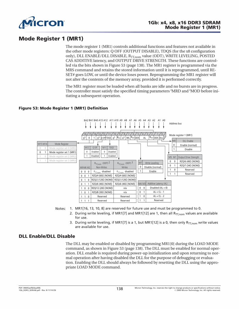
Mode Register 1 (MR1)The mode register 1 (MR1) controls additional functions and features not available inthe other mode registers: Q OFF (OUTPUT DISABLE), TDQS (for the x8 configurationonly), DLL ENABLE/DLL DISABLE, RTT,nom value (ODT), WRITE LEVELING, POSTEDCAS ADDITIVE latency, and OUTPUT DRIVE STRENGTH. These functions are control-led via the bits shown in Figure 53 (page 138). The MR1 register is programmed via theMRS command and retains the stored information until it is reprogrammed, until RE-SET# goes LOW, or until the device loses power. Reprogramming the MR1 register willnot alter the contents of the memory array, provided it is performed correctly.
The MR1 register must be loaded when all banks are idle and no bursts are in progress.The controller must satisfy the specified timing parameters tMRD and tMOD before ini-tiating a subsequent operation.
Figure 53: Mode Register 1 (MR1) Definition
AL RTTQ Off
A9 A7 A6 A5 A4 A3A8 A2 A1 A0
Mode register 1 (MR1)
Address bus
9 7 6 5 4 38 2 1 0
A10A12 A11BA0BA1
10111213
M0
0
1
DLL Enable
Enable (normal)
Disable
M5
0
0
1
1
Output Drive Strength
RZQ/6 (40 [NOM])
RZQ/7 (34 [NOM])
Reserved
Reserved
14
WL10 ODS DLLRTTTDQS
M12
0
1
Q Off
Enabled
Disabled
BA2
15
01
M7
0
1
Write Leveling
Disable (normal)
Enable
Additive Latency (AL)
Disabled (AL = 0)
AL = CL - 1
AL = CL - 2
Reserved
M3
0
1
0
1
M4
0
0
1
1
RTT ODS
M1
0
1
0
1
A13
16
01
M11
0
1
TDQS
Disabled
Enabled
01 01
RTT,nom (ODT) 2
Non-Writes
RTT,nom disabled
RZQ/4 (60 [NOM])
RZQ/2 (120 [NOM])
RZQ/6 (40 [NOM])
RZQ/12 (20 [NOM])
RZQ/8 (30 [NOM])
Reserved
Reserved
RTT,nom (ODT) 3
Writes
RTT,nom disabled
RZQ/4 (60 [NOM])
RZQ/2 (120 [NOM])
RZQ/6 (40 [NOM])
n/a
n/a
Reserved
Reserved
M2
0
1
0
1
0
1
0
1
M6
0
0
1
1
0
0
1
1
M9
0
0
0
0
1
1
1
1
Mode Register
Mode register set 0 (MR0)
Mode register set 1 (MR1)
Mode register set 2 (MR2)
Mode register set 3 (MR3)
M14
0
1
0
1
M15
0
0
1
1
Notes: 1. MR1[16, 13, 10, 8] are reserved for future use and must be programmed to 0.2. During write leveling, if MR1[7] and MR1[12] are 1, then all RTT,nom values are available
for use.3. During write leveling, if MR1[7] is a 1, but MR1[12] is a 0, then only RTT,nom write values
are available for use.
DLL Enable/DLL Disable
The DLL may be enabled or disabled by programming MR1[0] during the LOAD MODEcommand, as shown in Figure 53 (page 138). The DLL must be enabled for normal oper-ation. DLL enable is required during power-up initialization and upon returning to nor-mal operation after having disabled the DLL for the purpose of debugging or evalua-tion. Enabling the DLL should always be followed by resetting the DLL using the appro-priate LOAD MODE command.
1Gb: x4, x8, x16 DDR3 SDRAMMode Register 1 (MR1)
PDF: 09005aef826aa9061Gb_DDR3_SDRAM.pdf - Rev. N 11/14 EN 138 Micron Technology, Inc. reserves the right to change products or specifications without notice.
© 2006 Micron Technology, Inc. All rights reserved.
If the DLL is enabled prior to entering self refresh mode, the DLL is automatically disa-bled when entering SELF REFRESH operation and is automatically reenabled and resetupon exit of SELF REFRESH operation. If the DLL is disabled prior to entering self re-fresh mode, the DLL remains disabled even upon exit of SELF REFRESH operation untilit is reenabled and reset.
The DRAM is not tested to check—nor does Micron warrant compliance with—normalmode timings or functionality when the DLL is disabled. An attempt has been made tohave the DRAM operate in the normal mode where reasonably possible when the DLLhas been disabled; however, by industry standard, a few known exceptions are defined:
• ODT is not allowed to be used• The output data is no longer edge-aligned to the clock• CL and CWL can only be six clocks
When the DLL is disabled, timing and functionality can vary from the normal operationspecifications when the DLL is enabled (see DLL Disable Mode (page 120)). Disablingthe DLL also implies the need to change the clock frequency (see Input Clock Frequen-cy Change (page 124)).
Output Drive Strength
The DDR3 SDRAM uses a programmable impedance output buffer. The drive strengthmode register setting is defined by MR1[5, 1]. RZQ/7 (34Ω [NOM]) is the primary outputdriver impedance setting for DDR3 SDRAM devices. To calibrate the output driver im-pedance, an external precision resistor (RZQ) is connected between the ZQ ball andVSSQ. The value of the resistor must be 240Ω
The output impedance is set during initialization. Additional impedance calibration up-dates do not affect device operation, and all data sheet timings and current specifica-tions are met during an update.
To meet the 34Ω specification, the output drive strength must be set to 34Ω during initi-alization. To obtain a calibrated output driver impedance after power-up, the DDR3SDRAM needs a calibration command that is part of the initialization and reset proce-dure.
OUTPUT ENABLE/DISABLE
The OUTPUT ENABLE function is defined by MR1[12], as shown in Figure 53(page 138). When enabled (MR1[12] = 0), all outputs (DQ, DQS, DQS#) function when inthe normal mode of operation. When disabled (MR1[12] = 1), all DDR3 SDRAM outputs(DQ and DQS, DQS#) are tri-stated. The output disable feature is intended to be usedduring IDD characterization of the READ current and during tDQSS margining (writeleveling) only.
TDQS Enable
Termination data strobe (TDQS) is a feature of the x8 DDR3 SDRAM configuration thatprovides termination resistance (RTT) and may be useful in some system configurations.TDQS is not supported in x4 or x16 configurations. When enabled via the mode register(MR1[11]), the RTT that is applied to DQS and DQS# is also applied to TDQS and TDQS#.In contrast to the RDQS function of DDR2 SDRAM, DDR3’s TDQS provides the termina-tion resistance RTT only. The OUTPUT DATA STROBE function of RDQS is not providedby TDQS; thus, RON does not apply to TDQS and TDQS#. The TDQS and DM functions
1Gb: x4, x8, x16 DDR3 SDRAMMode Register 1 (MR1)
PDF: 09005aef826aa9061Gb_DDR3_SDRAM.pdf - Rev. N 11/14 EN 139 Micron Technology, Inc. reserves the right to change products or specifications without notice.
© 2006 Micron Technology, Inc. All rights reserved.
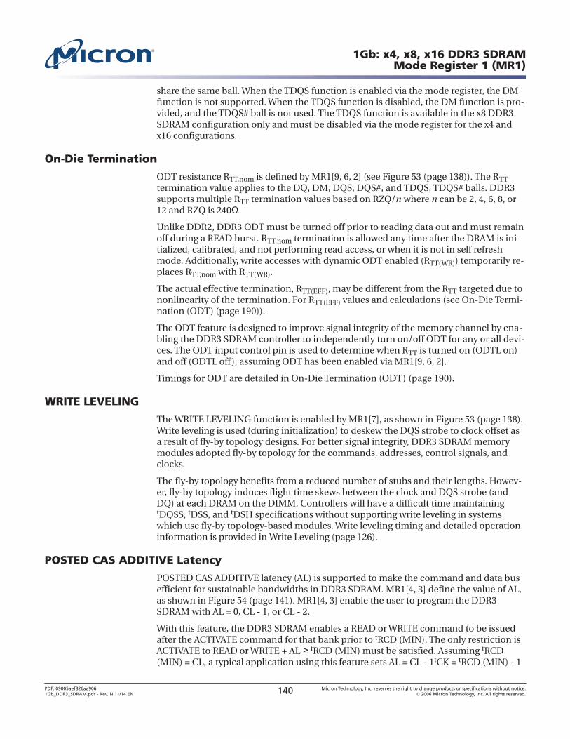
share the same ball. When the TDQS function is enabled via the mode register, the DMfunction is not supported. When the TDQS function is disabled, the DM function is pro-vided, and the TDQS# ball is not used. The TDQS function is available in the x8 DDR3SDRAM configuration only and must be disabled via the mode register for the x4 andx16 configurations.
On-Die Termination
ODT resistance RTT,nom is defined by MR1[9, 6, 2] (see Figure 53 (page 138)). The RTTtermination value applies to the DQ, DM, DQS, DQS#, and TDQS, TDQS# balls. DDR3supports multiple RTT termination values based on RZQ/n where n can be 2, 4, 6, 8, or12 and RZQ is 240Ω
Unlike DDR2, DDR3 ODT must be turned off prior to reading data out and must remainoff during a READ burst. RTT,nom termination is allowed any time after the DRAM is ini-tialized, calibrated, and not performing read access, or when it is not in self refreshmode. Additionally, write accesses with dynamic ODT enabled (RTT(WR)) temporarily re-places RTT,nom with RTT(WR).
The actual effective termination, RTT(EFF), may be different from the RTT targeted due tononlinearity of the termination. For RTT(EFF) values and calculations (see On-Die Termi-nation (ODT) (page 190)).
The ODT feature is designed to improve signal integrity of the memory channel by ena-bling the DDR3 SDRAM controller to independently turn on/off ODT for any or all devi-ces. The ODT input control pin is used to determine when RTT is turned on (ODTL on)and off (ODTL off), assuming ODT has been enabled via MR1[9, 6, 2].
Timings for ODT are detailed in On-Die Termination (ODT) (page 190).
WRITE LEVELING
The WRITE LEVELING function is enabled by MR1[7], as shown in Figure 53 (page 138).Write leveling is used (during initialization) to deskew the DQS strobe to clock offset asa result of fly-by topology designs. For better signal integrity, DDR3 SDRAM memorymodules adopted fly-by topology for the commands, addresses, control signals, andclocks.
The fly-by topology benefits from a reduced number of stubs and their lengths. Howev-er, fly-by topology induces flight time skews between the clock and DQS strobe (andDQ) at each DRAM on the DIMM. Controllers will have a difficult time maintainingtDQSS, tDSS, and tDSH specifications without supporting write leveling in systemswhich use fly-by topology-based modules. Write leveling timing and detailed operationinformation is provided in Write Leveling (page 126).
POSTED CAS ADDITIVE Latency
POSTED CAS ADDITIVE latency (AL) is supported to make the command and data busefficient for sustainable bandwidths in DDR3 SDRAM. MR1[4, 3] define the value of AL,as shown in Figure 54 (page 141). MR1[4, 3] enable the user to program the DDR3SDRAM with AL = 0, CL - 1, or CL - 2.
With this feature, the DDR3 SDRAM enables a READ or WRITE command to be issuedafter the ACTIVATE command for that bank prior to tRCD (MIN). The only restriction isACTIVATE to READ or WRITE + AL ≥ tRCD (MIN) must be satisfied. Assuming tRCD(MIN) = CL, a typical application using this feature sets AL = CL - 1tCK = tRCD (MIN) - 1
1Gb: x4, x8, x16 DDR3 SDRAMMode Register 1 (MR1)
PDF: 09005aef826aa9061Gb_DDR3_SDRAM.pdf - Rev. N 11/14 EN 140 Micron Technology, Inc. reserves the right to change products or specifications without notice.
© 2006 Micron Technology, Inc. All rights reserved.
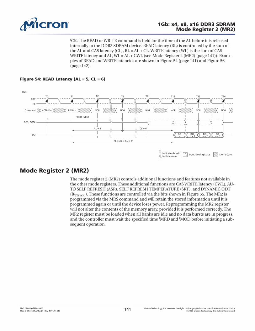
tCK. The READ or WRITE command is held for the time of the AL before it is releasedinternally to the DDR3 SDRAM device. READ latency (RL) is controlled by the sum ofthe AL and CAS latency (CL), RL = AL + CL. WRITE latency (WL) is the sum of CASWRITE latency and AL, WL = AL + CWL (see Mode Register 2 (MR2) (page 141)). Exam-ples of READ and WRITE latencies are shown in Figure 54 (page 141) and Figure 56(page 142).
Figure 54: READ Latency (AL = 5, CL = 6)
CK
CK#
Command
DQ
DQS, DQS#
ACTIVE n
T0 T1
Don’t Care
NOP NOP
T6 T12
NOPREAD n
T13
NOP
DOn + 3
DOn + 2
DOn + 1
RL = AL + CL = 11
T14
NOP
DOn
tRCD (MIN)
AL = 5 CL = 6
T11
BC4
Indicates breakin time scale
Transitioning Data
T2
NOP
Mode Register 2 (MR2)The mode register 2 (MR2) controls additional functions and features not available inthe other mode registers. These additional functions are CAS WRITE latency (CWL), AU-TO SELF REFRESH (ASR), SELF REFRESH TEMPERATURE (SRT), and DYNAMIC ODT(RTT(WR)). These functions are controlled via the bits shown in Figure 55. The MR2 isprogrammed via the MRS command and will retain the stored information until it isprogrammed again or until the device loses power. Reprogramming the MR2 registerwill not alter the contents of the memory array, provided it is performed correctly. TheMR2 register must be loaded when all banks are idle and no data bursts are in progress,and the controller must wait the specified time tMRD and tMOD before initiating a sub-sequent operation.
1Gb: x4, x8, x16 DDR3 SDRAMMode Register 2 (MR2)
PDF: 09005aef826aa9061Gb_DDR3_SDRAM.pdf - Rev. N 11/14 EN 141 Micron Technology, Inc. reserves the right to change products or specifications without notice.
© 2006 Micron Technology, Inc. All rights reserved.
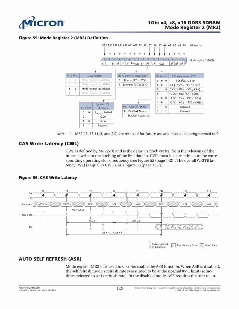
Figure 55: Mode Register 2 (MR2) Definition
M14
0
1
0
1
M15
0
0
1
1
Mode Register
Mode register set 0 (MR0)
Mode register set 1 (MR1)
Mode register set 2 (MR2)
Mode register set 3 (MR3)
A9 A7 A6 A5 A4 A3A8 A2 A1 A0
Mode register 2 (MR2)
Address bus
9 7 6 5 4 38 2 1 0
A10A12 A11BA0BA1
101112131415
1 CWL010
BA2
ASR
16
01
A13
01 01 01 01 0101 SRTRTT(WR)
M6
0
1
Auto Self Refresh
Disabled: Manual
Enabled: Automatic
M7
0
1
Self Refresh Temperature
Normal (0°C to 85°C)
Extended (0°C to 95°C)
CAS Write Latency (CWL)
5 CK (tCK ≥2.5ns)
6 CK (2.5ns tCK ≥1.875ns)
7 CK (1.875ns tCK ≥1.5ns)
8 CK (1.5ns tCK ≥1.25ns)
9 CK (1.25ns tCK ≥1.07ns)
10 CK (1.07ns tCK ≥0.938ns)
Reserved
Reserved
M3
0
1
0
1
0
1
0
1
M4
0
0
1
1
0
0
1
1
M5
0
0
0
0
1
1
1
1M9
0
1
0
1
M10
0
0
1
1
Dynamic ODT(RTT(WR) )
RTT(WR) disabled
RZQ/4
RZQ/2
Reserved
Note: 1. MR2[16, 13:11, 8, and 2:0] are reserved for future use and must all be programmed to 0.
CAS Write Latency (CWL)
CWL is defined by MR2[5:3] and is the delay, in clock cycles, from the releasing of theinternal write to the latching of the first data in. CWL must be correctly set to the corre-sponding operating clock frequency (see Figure 55 (page 142)). The overall WRITE la-tency (WL) is equal to CWL + AL (Figure 53 (page 138)).
Figure 56: CAS Write Latency
CK
CK#
Command
DQ
DQS, DQS#
ACTIVE n
T0 T1
Don’t Care
NOP NOP
T6 T12
NOPWRITE n
T13
NOP
DI n + 3
DI n + 2
DI n + 1
T14
NOP
DI n
tRCD (MIN)
NOP
AL = 5
T11
Indicates breakin time scale
WL = AL + CWL = 11
Transitioning Data
T2
CWL = 6
AUTO SELF REFRESH (ASR)
Mode register MR2[6] is used to disable/enable the ASR function. When ASR is disabled,the self refresh mode’s refresh rate is assumed to be at the normal 85°C limit (some-times referred to as 1x refresh rate). In the disabled mode, ASR requires the user to en-
1Gb: x4, x8, x16 DDR3 SDRAMMode Register 2 (MR2)
PDF: 09005aef826aa9061Gb_DDR3_SDRAM.pdf - Rev. N 11/14 EN 142 Micron Technology, Inc. reserves the right to change products or specifications without notice.
© 2006 Micron Technology, Inc. All rights reserved.
sure the DRAM never exceeds a TC of 85°C while in self refresh unless the user enablesthe SRT feature listed below when the TC is between 85°C and 95°C.
Enabling ASR assumes the DRAM self refresh rate is changed automatically from 1x to2x when the case temperature exceeds 85°C. This enables the user to operate the DRAMbeyond the standard 85°C limit up to the optional extended temperature range of 95°Cwhile in self refresh mode.
The standard self refresh current test specifies test conditions to normal case tempera-ture (85°C) only, meaning if ASR is enabled, the standard self refresh current specifica-tions do not apply (see Extended Temperature Usage (page 179)).
SELF REFRESH TEMPERATURE (SRT)
Mode register MR2[7] is used to disable/enable the SRT function. When SRT is disabled,the self refresh mode’s refresh rate is assumed to be at the normal 85°C limit (some-times referred to as 1x refresh rate). In the disabled mode, SRT requires the user to en-sure the DRAM never exceeds a TC of 85°C while in self refresh mode unless the user en-ables ASR.
When SRT is enabled, the DRAM self refresh is changed internally from 1x to 2x, regard-less of the case temperature. This enables the user to operate the DRAM beyond thestandard 85°C limit up to the optional extended temperature range of 95°C while in selfrefresh mode. The standard self refresh current test specifies test conditions to normalcase temperature (85°C) only, meaning if SRT is enabled, the standard self refresh cur-rent specifications do not apply (see Extended Temperature Usage (page 179)).
SRT vs. ASR
If the normal case temperature limit of 85°C is not exceeded, then neither SRT nor ASRis required, and both can be disabled throughout operation. However, if the extendedtemperature option of 95°C is needed, the user is required to provide a 2x refresh rateduring (manual) refresh and to enable either the SRT or the ASR to ensure self refresh isperformed at the 2x rate.
SRT forces the DRAM to switch the internal self refresh rate from 1x to 2x. Self refresh isperformed at the 2x refresh rate regardless of the case temperature.
ASR automatically switches the DRAM’s internal self refresh rate from 1x to 2x. Howev-er, while in self refresh mode, ASR enables the refresh rate to automatically adjust be-tween 1x to 2x over the supported temperature range. One other disadvantage with ASRis the DRAM cannot always switch from a 1x to a 2x refresh rate at an exact case temper-ature of 85°C. Although the DRAM will support data integrity when it switches from a 1xto a 2x refresh rate, it may switch at a lower temperature than 85°C.
Since only one mode is necessary, SRT and ASR cannot be enabled at the same time.
DYNAMIC ODT
The dynamic ODT (RTT(WR)) feature is defined by MR2[10, 9]. Dynamic ODT is enabledwhen a value is selected. This new DDR3 SDRAM feature enables the ODT terminationvalue to change without issuing an MRS command, essentially changing the ODT ter-mination on-the-fly.
With dynamic ODT (RTT(WR)) enabled, the DRAM switches from normal ODT (RTT,nom)to dynamic ODT (RTT(WR)) when beginning a WRITE burst and subsequently switches
1Gb: x4, x8, x16 DDR3 SDRAMMode Register 2 (MR2)
PDF: 09005aef826aa9061Gb_DDR3_SDRAM.pdf - Rev. N 11/14 EN 143 Micron Technology, Inc. reserves the right to change products or specifications without notice.
© 2006 Micron Technology, Inc. All rights reserved.
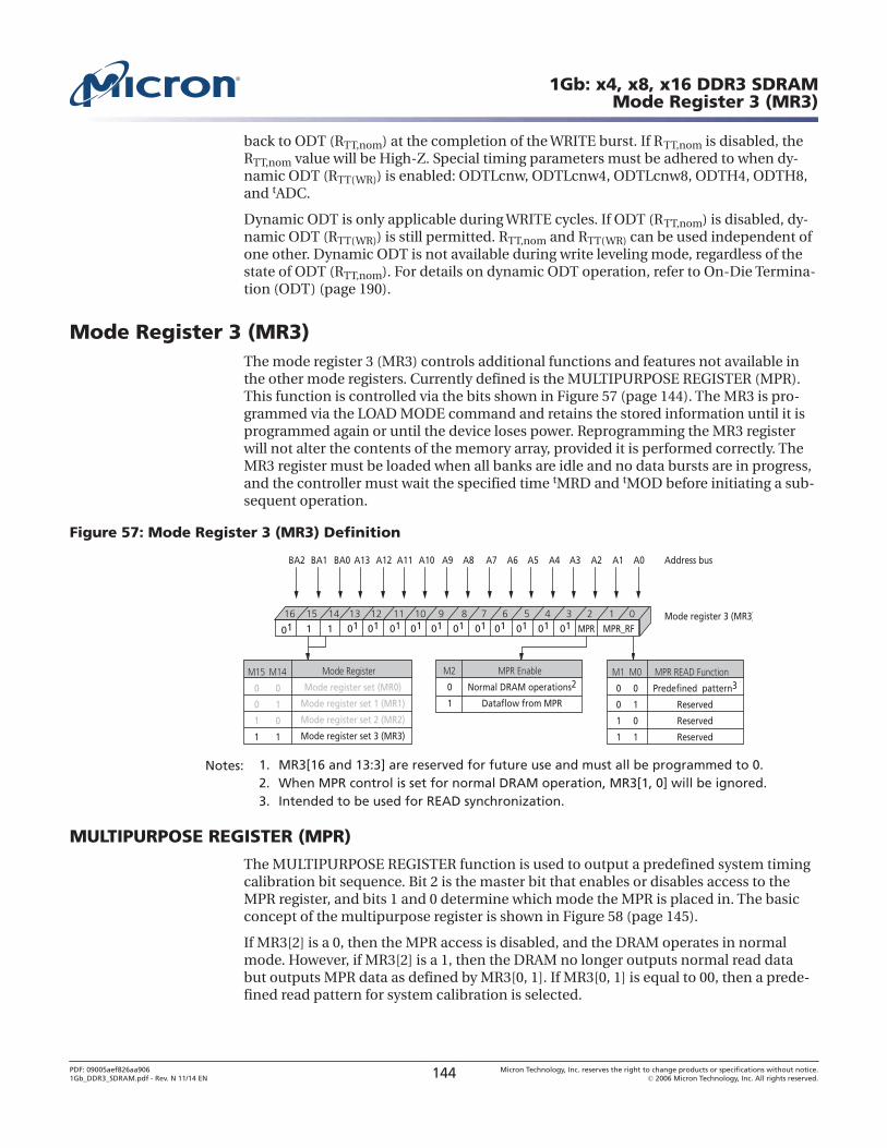
back to ODT (RTT,nom) at the completion of the WRITE burst. If RTT,nom is disabled, theRTT,nom value will be High-Z. Special timing parameters must be adhered to when dy-namic ODT (RTT(WR)) is enabled: ODTLcnw, ODTLcnw4, ODTLcnw8, ODTH4, ODTH8,and tADC.
Dynamic ODT is only applicable during WRITE cycles. If ODT (RTT,nom) is disabled, dy-namic ODT (RTT(WR)) is still permitted. RTT,nom and RTT(WR) can be used independent ofone other. Dynamic ODT is not available during write leveling mode, regardless of thestate of ODT (RTT,nom). For details on dynamic ODT operation, refer to On-Die Termina-tion (ODT) (page 190).
Mode Register 3 (MR3)The mode register 3 (MR3) controls additional functions and features not available inthe other mode registers. Currently defined is the MULTIPURPOSE REGISTER (MPR).This function is controlled via the bits shown in Figure 57 (page 144). The MR3 is pro-grammed via the LOAD MODE command and retains the stored information until it isprogrammed again or until the device loses power. Reprogramming the MR3 registerwill not alter the contents of the memory array, provided it is performed correctly. TheMR3 register must be loaded when all banks are idle and no data bursts are in progress,and the controller must wait the specified time tMRD and tMOD before initiating a sub-sequent operation.
Figure 57: Mode Register 3 (MR3) Definition
A9 A7 A6 A5 A4 A3A8 A2 A1 A0
Mode register 3 (MR3)
Address bus
9 7 6 5 4 38 2 1 0
A10A12 A11BA0BA1
101112131415
A13
1 01 01 01 01 01 01 01 MPR 1
BA2
16
01 01 01 01 01
M2
0
1
MPR Enable
Normal DRAM operations2
Dataflow from MPR
MPR_RF
M14
0
1
0
1
M15
0
0
1
1
Mode Register
Mode register set (MR0)
Mode register set 1 (MR1)
Mode register set 2 (MR2)
Mode register set 3 (MR3)
MPR READ Function
Predefined pattern3
Reserved
Reserved
Reserved
M0
0
1
0
1
M1
0
0
1
1
Notes: 1. MR3[16 and 13:3] are reserved for future use and must all be programmed to 0.2. When MPR control is set for normal DRAM operation, MR3[1, 0] will be ignored.3. Intended to be used for READ synchronization.
MULTIPURPOSE REGISTER (MPR)
The MULTIPURPOSE REGISTER function is used to output a predefined system timingcalibration bit sequence. Bit 2 is the master bit that enables or disables access to theMPR register, and bits 1 and 0 determine which mode the MPR is placed in. The basicconcept of the multipurpose register is shown in Figure 58 (page 145).
If MR3[2] is a 0, then the MPR access is disabled, and the DRAM operates in normalmode. However, if MR3[2] is a 1, then the DRAM no longer outputs normal read databut outputs MPR data as defined by MR3[0, 1]. If MR3[0, 1] is equal to 00, then a prede-fined read pattern for system calibration is selected.
1Gb: x4, x8, x16 DDR3 SDRAMMode Register 3 (MR3)
PDF: 09005aef826aa9061Gb_DDR3_SDRAM.pdf - Rev. N 11/14 EN 144 Micron Technology, Inc. reserves the right to change products or specifications without notice.
© 2006 Micron Technology, Inc. All rights reserved.
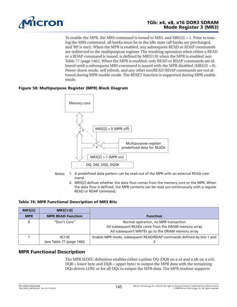
To enable the MPR, the MRS command is issued to MR3, and MR3[2] = 1. Prior to issu-ing the MRS command, all banks must be in the idle state (all banks are precharged,and tRP is met). When the MPR is enabled, any subsequent READ or RDAP commandsare redirected to the multipurpose register. The resulting operation when either a READor a RDAP command is issued, is defined by MR3[1:0] when the MPR is enabled (seeTable 77 (page 146)). When the MPR is enabled, only READ or RDAP commands are al-lowed until a subsequent MRS command is issued with the MPR disabled (MR3[2] = 0).Power-down mode, self refresh, and any other nonREAD/RDAP commands are not al-lowed during MPR enable mode. The RESET function is supported during MPR enablemode.
Figure 58: Multipurpose Register (MPR) Block Diagram
Memory core
MR3[2] = 0 (MPR off)
DQ, DM, DQS, DQS#
Multipurpose registerpredefined data for READs
MR3[2] = 1 (MPR on)
Notes: 1. A predefined data pattern can be read out of the MPR with an external READ com-mand.
2. MR3[2] defines whether the data flow comes from the memory core or the MPR. Whenthe data flow is defined, the MPR contents can be read out continuously with a regularREAD or RDAP command.
Table 76: MPR Functional Description of MR3 Bits
MR3[2] MR3[1:0]
FunctionMPR MPR READ Function
0 “Don’t Care” Normal operation, no MPR transactionAll subsequent READs come from the DRAM memory array
All subsequent WRITEs go to the DRAM memory array
1 A[1:0](see Table 77 (page 146))
Enable MPR mode, subsequent READ/RDAP commands defined by bits 1 and2
MPR Functional Description
The MPR JEDEC definition enables either a prime DQ (DQ0 on a x4 and a x8; on a x16,DQ0 = lower byte and DQ8 = upper byte) to output the MPR data with the remainingDQs driven LOW, or for all DQs to output the MPR data. The MPR readout supports
1Gb: x4, x8, x16 DDR3 SDRAMMode Register 3 (MR3)
PDF: 09005aef826aa9061Gb_DDR3_SDRAM.pdf - Rev. N 11/14 EN 145 Micron Technology, Inc. reserves the right to change products or specifications without notice.
© 2006 Micron Technology, Inc. All rights reserved.
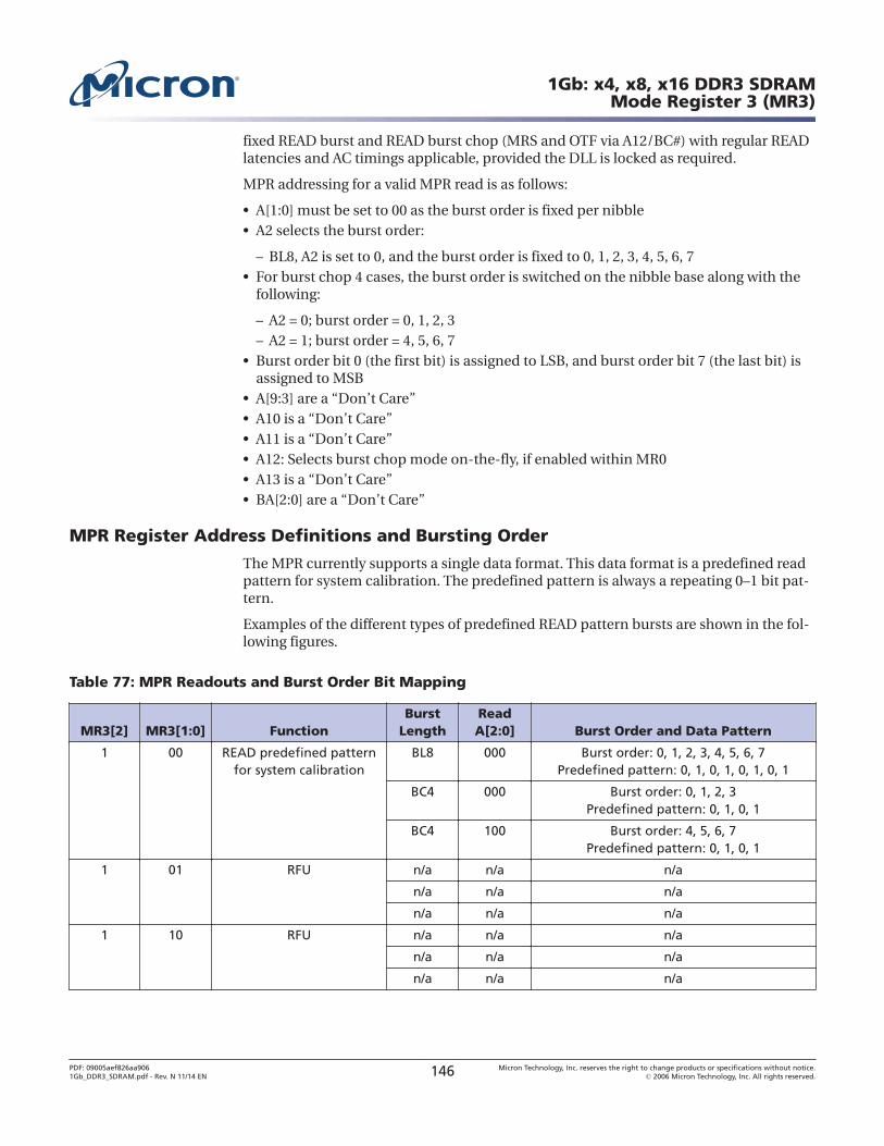
fixed READ burst and READ burst chop (MRS and OTF via A12/BC#) with regular READlatencies and AC timings applicable, provided the DLL is locked as required.
MPR addressing for a valid MPR read is as follows:
• A[1:0] must be set to 00 as the burst order is fixed per nibble• A2 selects the burst order:
– BL8, A2 is set to 0, and the burst order is fixed to 0, 1, 2, 3, 4, 5, 6, 7• For burst chop 4 cases, the burst order is switched on the nibble base along with the
following:
– A2 = 0; burst order = 0, 1, 2, 3– A2 = 1; burst order = 4, 5, 6, 7
• Burst order bit 0 (the first bit) is assigned to LSB, and burst order bit 7 (the last bit) isassigned to MSB
• A[9:3] are a “Don’t Care”• A10 is a “Don’t Care”• A11 is a “Don’t Care”• A12: Selects burst chop mode on-the-fly, if enabled within MR0• A13 is a “Don’t Care”• BA[2:0] are a “Don’t Care”
MPR Register Address Definitions and Bursting Order
The MPR currently supports a single data format. This data format is a predefined readpattern for system calibration. The predefined pattern is always a repeating 0–1 bit pat-tern.
Examples of the different types of predefined READ pattern bursts are shown in the fol-lowing figures.
Table 77: MPR Readouts and Burst Order Bit Mapping
MR3[2] MR3[1:0] FunctionBurst
LengthReadA[2:0] Burst Order and Data Pattern
1 00 READ predefined patternfor system calibration
BL8 000 Burst order: 0, 1, 2, 3, 4, 5, 6, 7Predefined pattern: 0, 1, 0, 1, 0, 1, 0, 1
BC4 000 Burst order: 0, 1, 2, 3Predefined pattern: 0, 1, 0, 1
BC4 100 Burst order: 4, 5, 6, 7Predefined pattern: 0, 1, 0, 1
1 01 RFU n/a n/a n/a
n/a n/a n/a
n/a n/a n/a
1 10 RFU n/a n/a n/a
n/a n/a n/a
n/a n/a n/a
1Gb: x4, x8, x16 DDR3 SDRAMMode Register 3 (MR3)
PDF: 09005aef826aa9061Gb_DDR3_SDRAM.pdf - Rev. N 11/14 EN 146 Micron Technology, Inc. reserves the right to change products or specifications without notice.
© 2006 Micron Technology, Inc. All rights reserved.
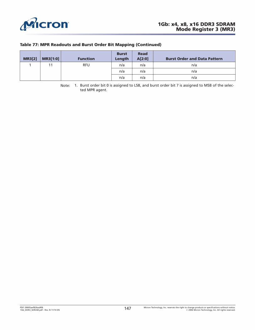
Table 77: MPR Readouts and Burst Order Bit Mapping (Continued)
MR3[2] MR3[1:0] FunctionBurst
LengthReadA[2:0] Burst Order and Data Pattern
1 11 RFU n/a n/a n/a
n/a n/a n/a
n/a n/a n/a
Note: 1. Burst order bit 0 is assigned to LSB, and burst order bit 7 is assigned to MSB of the selec-ted MPR agent.
1Gb: x4, x8, x16 DDR3 SDRAMMode Register 3 (MR3)
PDF: 09005aef826aa9061Gb_DDR3_SDRAM.pdf - Rev. N 11/14 EN 147 Micron Technology, Inc. reserves the right to change products or specifications without notice.
© 2006 Micron Technology, Inc. All rights reserved.
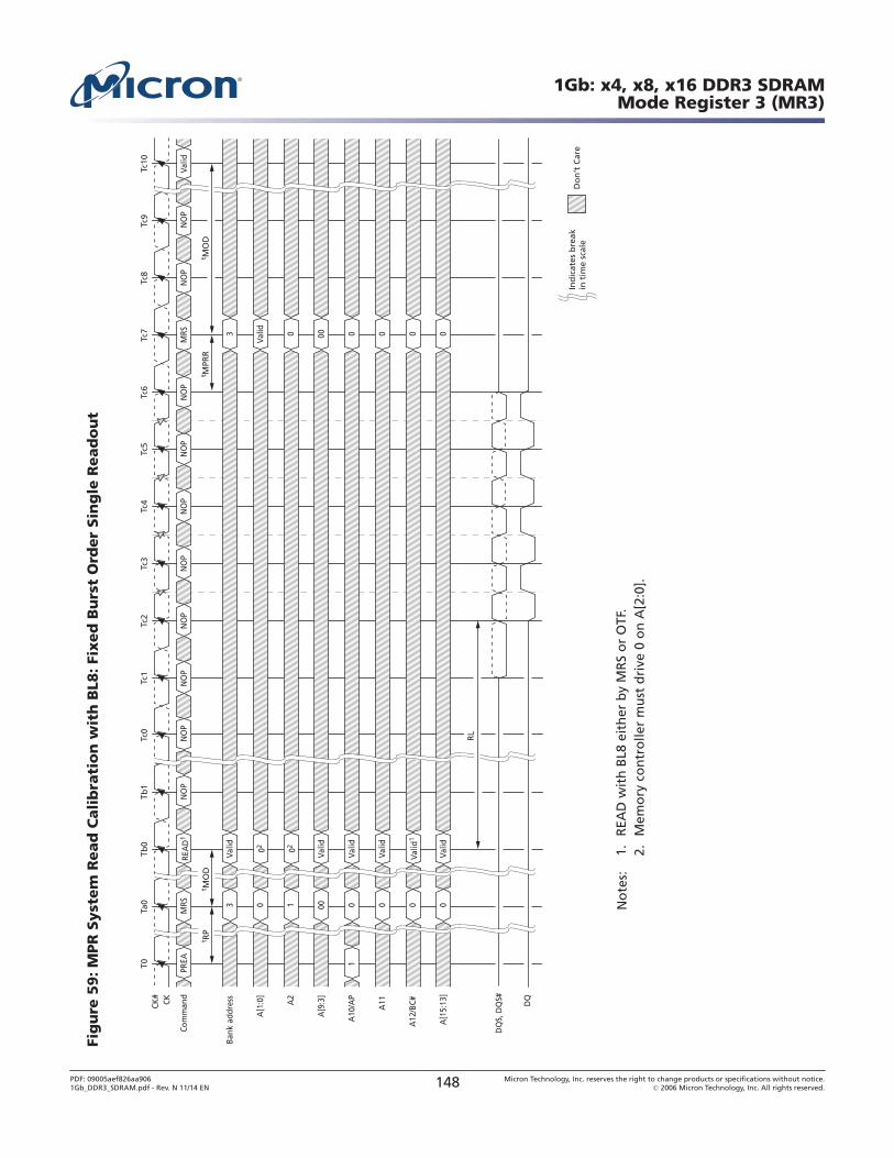
Fig
ure
59
: M
PR
Syst
em
Read
Cali
bra
tio
n w
ith
BL8
: Fi
xed
Bu
rst
Ord
er
Sin
gle
Read
ou
t
T0
Ta0
Tb0
Tb1
Tc0
Tc1
Tc2
Tc3
Tc4
Tc5
Tc6
Tc7
Tc8
Tc9
Tc10
CKCK#
MRS
PREA
REA
D1
NO
PN
OP
NO
PN
OP
NO
PN
OP
NO
PN
OP
MRS
NO
PN
OP
Valid
Com
man
d
t MPR
R
Do
n’t
Car
eIn
dic
ates
bre
akin
tim
e sc
ale
DQ
S, D
QS#
Bank
add
ress
3Va
lid3
0A
[1:0
]Va
lid02
1A
202
0
00A
[9:3
]Va
lid00
01
A10
/AP
Valid
0
0A
11Va
lid0
0A
12/B
C#Va
lid1
0
0A
[15:
13]
Valid
0
DQ
t MO
Dt R
Pt M
OD
RL
No
tes:
1.R
EAD
wit
h B
L8 e
ith
er b
y M
RS
or
OTF
.2.
Mem
ory
co
ntr
olle
r m
ust
dri
ve 0
on
A[2
:0].
1Gb: x4, x8, x16 DDR3 SDRAMMode Register 3 (MR3)
PDF: 09005aef826aa9061Gb_DDR3_SDRAM.pdf - Rev. N 11/14 EN 148 Micron Technology, Inc. reserves the right to change products or specifications without notice.
© 2006 Micron Technology, Inc. All rights reserved.
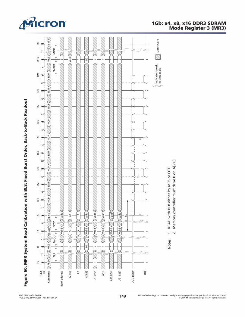
Fig
ure
60
: M
PR
Syst
em
Read
Cali
bra
tio
n w
ith
BL8
: Fi
xed
Bu
rst
Ord
er,
Back
-to
-Back
Read
ou
t
T0
TaTb
Tc0
Tc1
Tc2
Tc3
Tc4
Tc5
Tc6
Tc7
Tc8
Tc9
Tc10
Td
CKCK#
t MPR
R
Do
n’t
Car
eIn
dic
ates
bre
akin
tim
e sc
ale
RL
3Va
lid3
Bank
add
ress
Valid
A[1
:0]
Valid
0202
0
A2
1202
10
0A
[15:
13]
Valid
Valid
0
A[9
:3]
Valid
Valid
0000
A11
Valid
Valid
00
A12
/BC#
Valid
10
0
A10
/AP
Valid
Valid
00
1
RL
PREA
REA
D1
NO
PN
OP
NO
PN
OP
NO
PN
OP
NO
PN
OP
NO
PM
RSVa
lidCo
mm
and
REA
D1
MRS
DQ
Valid
DQ
S, D
QS#
t RP
t MO
Dt C
CD
t MO
D
No
tes:
1.R
EAD
wit
h B
L8 e
ith
er b
y M
RS
or
OTF
.2.
Mem
ory
co
ntr
olle
r m
ust
dri
ve 0
on
A[2
:0].
1Gb: x4, x8, x16 DDR3 SDRAMMode Register 3 (MR3)
PDF: 09005aef826aa9061Gb_DDR3_SDRAM.pdf - Rev. N 11/14 EN 149 Micron Technology, Inc. reserves the right to change products or specifications without notice.
© 2006 Micron Technology, Inc. All rights reserved.
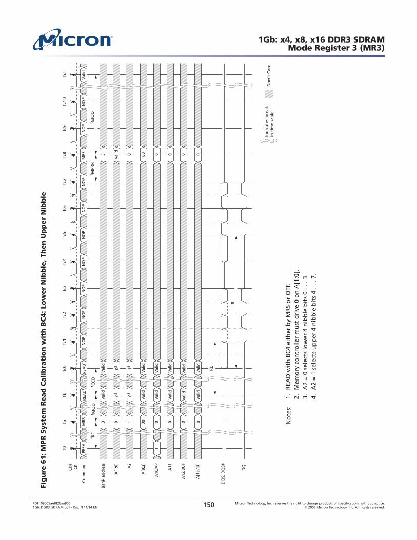
Fig
ure
61
: M
PR
Syst
em
Read
Cali
bra
tio
n w
ith
BC
4: Lo
wer
Nib
ble
, Th
en
Up
per
Nib
ble
T0
TaTb
CKCK#
DQ
DQ
S, D
QS#
t MO
Dt M
PRR
Do
n’t
Car
e
Tc0
Tc1
Tc2
Tc3
Tc4
Tc5
Tc6
Tc7
Tc8
Tc9
Tc10
Td
NO
PN
OP
NO
PN
OP
NO
PM
RSN
OP
NO
PVa
lidCo
mm
and
MRS
PREA
REA
D1
REA
D1
NO
PN
OP
Ind
icat
es b
reak
in t
ime
scal
e
Bank
add
ress
3Va
lid3
Valid
0A
[1:0
]Va
lid02
02
1A
214
030
00A
[9:3
]Va
lidVa
lid00
01
A10
/AP
Valid
Valid
0
0A
11Va
lidVa
lid0
0A
12/B
C#Va
lid1
Valid
10
0A
[15:
13]
Valid
Valid
0
RL
RL
t RF
t MO
Dt C
CD
No
tes:
1.R
EAD
wit
h B
C4
eith
er b
y M
RS
or
OTF
.2.
Mem
ory
co
ntr
olle
r m
ust
dri
ve 0
on
A[1
:0].
3.A
2 =
0 s
elec
ts lo
wer
4 n
ibb
le b
its
0 . .
. 3.
4.A
2 =
1 s
elec
ts u
pp
er 4
nib
ble
bit
s 4
. . .
7.
1Gb: x4, x8, x16 DDR3 SDRAMMode Register 3 (MR3)
PDF: 09005aef826aa9061Gb_DDR3_SDRAM.pdf - Rev. N 11/14 EN 150 Micron Technology, Inc. reserves the right to change products or specifications without notice.
© 2006 Micron Technology, Inc. All rights reserved.

Fig
ure
62
: M
PR
Syst
em
Read
Cali
bra
tio
n w
ith
BC
4: U
pp
er
Nib
ble
, Th
en
Lo
wer
Nib
ble
T0
TaTb
01
A10
/AP
Valid
Valid
0
CKCK#
MRS
PREA
REA
D1
REA
D1
NO
PN
OP
NO
PN
OP
NO
PN
OP
NO
PM
RSN
OP
NO
PVa
lidCo
mm
and
004
131
A2
t MO
Dt M
PRR
3Va
lid3
Bank
add
ress
Valid 02
020
A[1
:0]
Valid 0
0A
[15:
13]
Valid
Valid
00
A11
Valid
Valid
0000
A[9
:3]
Valid
Valid
Do
n’t
Car
e
Tc0
Tc1
Tc2
Tc3
Tc4
Tc5
Tc6
Tc7
Tc8
Tc9
Tc10
Td
Ind
icat
es b
reak
in t
ime
scal
e
RL
DQ
DQ
S, D
QS#
0A
12/B
C#Va
lid1
Valid
10
RL
t RF
t MO
Dt C
CD
No
tes:
1.R
EAD
wit
h B
C4
eith
er b
y M
RS
or
OTF
.2.
Mem
ory
co
ntr
olle
r m
ust
dri
ve 0
on
A[1
:0].
3.A
2 =
1 s
elec
ts u
pp
er 4
nib
ble
bit
s 4
. . .
7.4.
A2
= 0
sel
ects
low
er 4
nib
ble
bit
s 0
. . .
3.
1Gb: x4, x8, x16 DDR3 SDRAMMode Register 3 (MR3)
PDF: 09005aef826aa9061Gb_DDR3_SDRAM.pdf - Rev. N 11/14 EN 151 Micron Technology, Inc. reserves the right to change products or specifications without notice.
© 2006 Micron Technology, Inc. All rights reserved.
MPR Read Predefined Pattern
The predetermined read calibration pattern is a fixed pattern of 0, 1, 0, 1, 0, 1, 0, 1. Thefollowing is an example of using the read out predetermined read calibration pattern.The example is to perform multiple reads from the multipurpose register to do systemlevel read timing calibration based on the predetermined and standardized pattern.
The following protocol outlines the steps used to perform the read calibration:1. Precharge all banks2. After tRP is satisfied, set MRS, MR3[2] = 1 and MR3[1:0] = 00. This redirects all sub-
sequent reads and loads the predefined pattern into the MPR. As soon as tMRDand tMOD are satisfied, the MPR is available
3. Data WRITE operations are not allowed until the MPR returns to the normalDRAM state
4. Issue a read with burst order information (all other address pins are “Don’t Care”):
• A[1:0] = 00 (data burst order is fixed starting at nibble)• A2 = 0 (for BL8, burst order is fixed as 0, 1, 2, 3, 4, 5, 6, 7)• A12 = 1 (use BL8)
5. After RL = AL + CL, the DRAM bursts out the predefined read calibration pattern(0, 1, 0, 1, 0, 1, 0, 1)
6. The memory controller repeats the calibration reads until read data capture atmemory controller is optimized
7. After the last MPR READ burst and after tMPRR has been satisfied, issue MRS,MR3[2] = 0, and MR3[1:0] = “Don’t Care” to the normal DRAM state. All subse-quent read and write accesses will be regular reads and writes from/to the DRAMarray
8. When tMRD and tMOD are satisfied from the last MRS, the regular DRAM com-mands (such as activate a memory bank for regular read or write access) are per-mitted
MODE REGISTER SET (MRS) CommandThe mode registers are loaded via inputs BA[2:0], A[13:0]. BA[2:0] determine whichmode register is programmed:
• BA2 = 0, BA1 = 0, BA0 = 0 for MR0• BA2 = 0, BA1 = 0, BA0 = 1 for MR1• BA2 = 0, BA1 = 1, BA0 = 0 for MR2• BA2 = 0, BA1 = 1, BA0 = 1 for MR3
The MRS command can only be issued (or re-issued) when all banks are idle and in theprecharged state (tRP is satisfied and no data bursts are in progress). The controllermust wait the specified time tMRD before initiating a subsequent operation such as anACTIVATE command (see Figure 49 (page 133)). There is also a restriction after issuingan MRS command with regard to when the updated functions become available. Thisparameter is specified by tMOD. Both tMRD and tMOD parameters are shown in Fig-ure 49 (page 133) and Figure 50 (page 134). Violating either of these requirements willresult in unspecified operation.
1Gb: x4, x8, x16 DDR3 SDRAMMODE REGISTER SET (MRS) Command
PDF: 09005aef826aa9061Gb_DDR3_SDRAM.pdf - Rev. N 11/14 EN 152 Micron Technology, Inc. reserves the right to change products or specifications without notice.
© 2006 Micron Technology, Inc. All rights reserved.
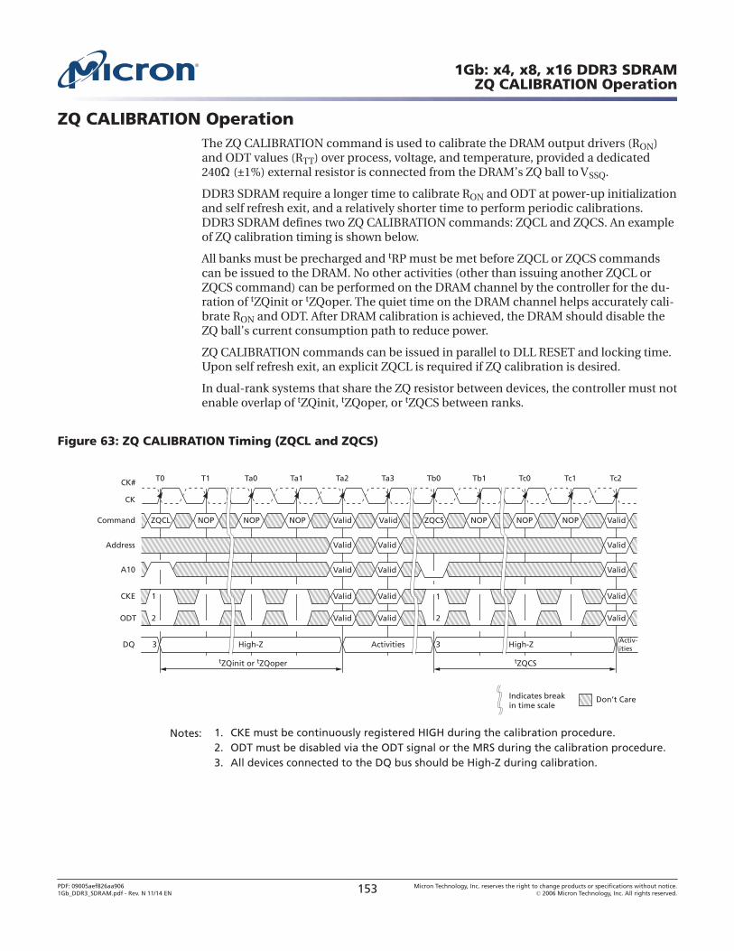
ZQ CALIBRATION OperationThe ZQ CALIBRATION command is used to calibrate the DRAM output drivers (RON)and ODT values (RTT) over process, voltage, and temperature, provided a dedicated240Ω (±1%) external resistor is connected from the DRAM’s ZQ ball to VSSQ.
DDR3 SDRAM require a longer time to calibrate RON and ODT at power-up initializationand self refresh exit, and a relatively shorter time to perform periodic calibrations.DDR3 SDRAM defines two ZQ CALIBRATION commands: ZQCL and ZQCS. An exampleof ZQ calibration timing is shown below.
All banks must be precharged and tRP must be met before ZQCL or ZQCS commandscan be issued to the DRAM. No other activities (other than issuing another ZQCL orZQCS command) can be performed on the DRAM channel by the controller for the du-ration of tZQinit or tZQoper. The quiet time on the DRAM channel helps accurately cali-brate RON and ODT. After DRAM calibration is achieved, the DRAM should disable theZQ ball’s current consumption path to reduce power.
ZQ CALIBRATION commands can be issued in parallel to DLL RESET and locking time.Upon self refresh exit, an explicit ZQCL is required if ZQ calibration is desired.
In dual-rank systems that share the ZQ resistor between devices, the controller must notenable overlap of tZQinit, tZQoper, or tZQCS between ranks.
Figure 63: ZQ CALIBRATION Timing (ZQCL and ZQCS)
NOPZQCL NOP NOP Valid Valid ZQCS NOP NOP NOP ValidCommand
Indicates breakin time scale
T0 T1 Ta0 Ta1 Ta2 Ta3 Tb0 Tb1 Tc0 Tc1 Tc2
Address Valid ValidValid
A10 Valid ValidValid
CK
CK#
Don’t Care
DQ High-Z High-Z33 Activities Activ-ities
Valid ValidODT 2 2 Valid
1CKE 1 Valid Valid Valid
tZQCStZQinit or tZQoper
Notes: 1. CKE must be continuously registered HIGH during the calibration procedure.2. ODT must be disabled via the ODT signal or the MRS during the calibration procedure.3. All devices connected to the DQ bus should be High-Z during calibration.
1Gb: x4, x8, x16 DDR3 SDRAMZQ CALIBRATION Operation
PDF: 09005aef826aa9061Gb_DDR3_SDRAM.pdf - Rev. N 11/14 EN 153 Micron Technology, Inc. reserves the right to change products or specifications without notice.
© 2006 Micron Technology, Inc. All rights reserved.
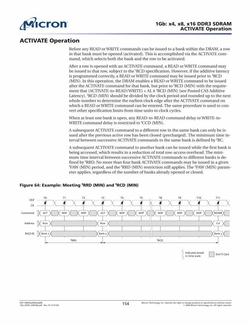
ACTIVATE OperationBefore any READ or WRITE commands can be issued to a bank within the DRAM, a rowin that bank must be opened (activated). This is accomplished via the ACTIVATE com-mand, which selects both the bank and the row to be activated.
After a row is opened with an ACTIVATE command, a READ or WRITE command maybe issued to that row, subject to the tRCD specification. However, if the additive latencyis programmed correctly, a READ or WRITE command may be issued prior to tRCD(MIN). In this operation, the DRAM enables a READ or WRITE command to be issuedafter the ACTIVATE command for that bank, but prior to tRCD (MIN) with the require-ment that (ACTIVATE-to-READ/WRITE) + AL ≥ tRCD (MIN) (see Posted CAS AdditiveLatency). tRCD (MIN) should be divided by the clock period and rounded up to the nextwhole number to determine the earliest clock edge after the ACTIVATE command onwhich a READ or WRITE command can be entered. The same procedure is used to con-vert other specification limits from time units to clock cycles.
When at least one bank is open, any READ-to-READ command delay or WRITE-to-WRITE command delay is restricted to tCCD (MIN).
A subsequent ACTIVATE command to a different row in the same bank can only be is-sued after the previous active row has been closed (precharged). The minimum time in-terval between successive ACTIVATE commands to the same bank is defined by tRC.
A subsequent ACTIVATE command to another bank can be issued while the first bank isbeing accessed, which results in a reduction of total row-access overhead. The mini-mum time interval between successive ACTIVATE commands to different banks is de-fined by tRRD. No more than four bank ACTIVATE commands may be issued in a giventFAW (MIN) period, and the tRRD (MIN) restriction still applies. The tFAW (MIN) param-eter applies, regardless of the number of banks already opened or closed.
Figure 64: Example: Meeting tRRD (MIN) and tRCD (MIN)
Command
Don’t Care
T1T0 T2 T3 T4 T5 T8 T9
tRRD
Row Row Col
Bank x Bank y Bank y
NOPACT NOP NOPACT NOP NOP RD/WR
tRCD
BA[2:0]
CK#
Address
CK
T10 T11
NOP NOP
Indicates breakin time scale
1Gb: x4, x8, x16 DDR3 SDRAMACTIVATE Operation
PDF: 09005aef826aa9061Gb_DDR3_SDRAM.pdf - Rev. N 11/14 EN 154 Micron Technology, Inc. reserves the right to change products or specifications without notice.
© 2006 Micron Technology, Inc. All rights reserved.
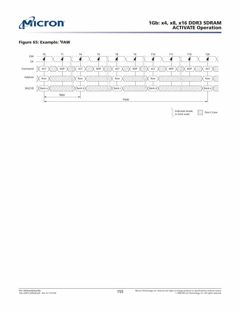
Figure 65: Example: tFAW
Command
Don’t Care
T1T0 T4 T5 T8 T9 T10 T11
tRRD
Row Row
Bank a Bank b
Row
Bank c
Row
Bank d Bank y
Row
Bank y
NOPACT NOPACT ACT NOP NOP
tFAW
BA[2:0]
CK#
Address
CK
T19 T20
NOPACT ACT
Bank e
Indicates breakin time scale
1Gb: x4, x8, x16 DDR3 SDRAMACTIVATE Operation
PDF: 09005aef826aa9061Gb_DDR3_SDRAM.pdf - Rev. N 11/14 EN 155 Micron Technology, Inc. reserves the right to change products or specifications without notice.
© 2006 Micron Technology, Inc. All rights reserved.
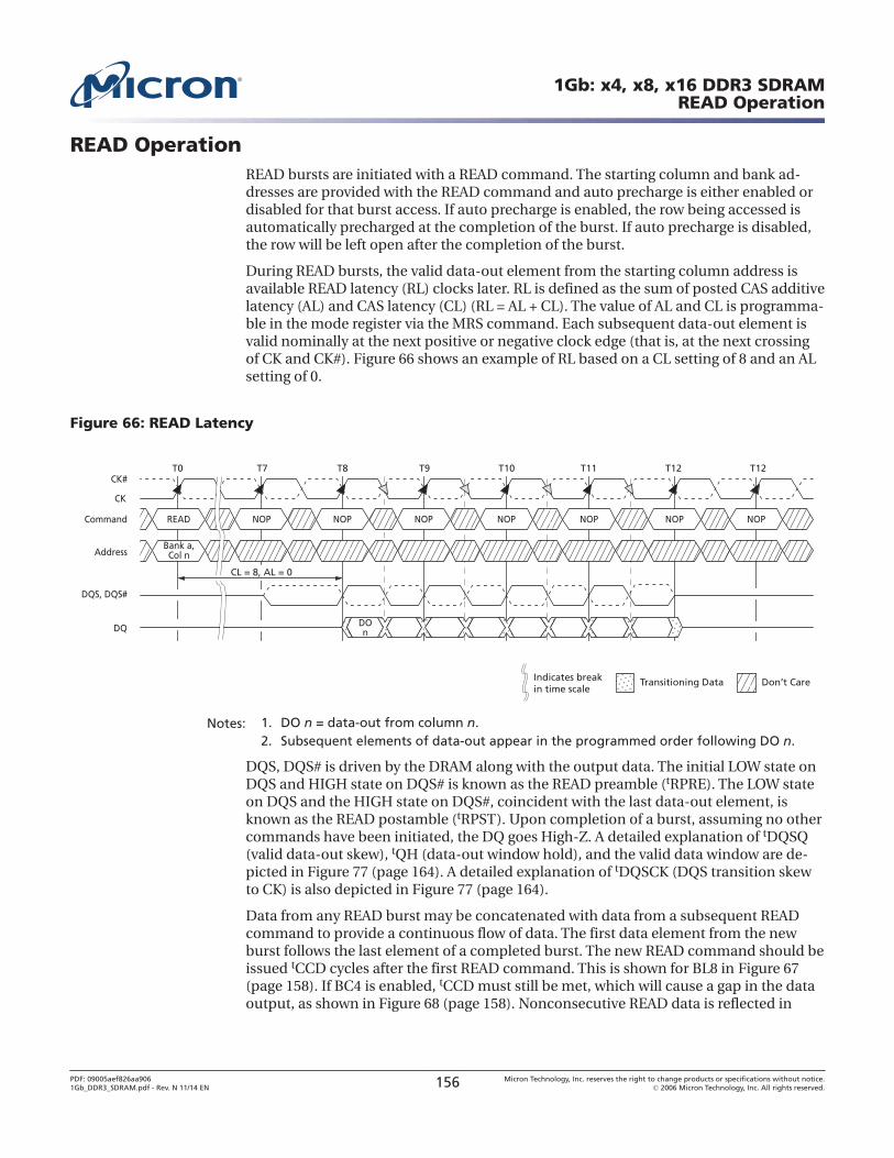
READ OperationREAD bursts are initiated with a READ command. The starting column and bank ad-dresses are provided with the READ command and auto precharge is either enabled ordisabled for that burst access. If auto precharge is enabled, the row being accessed isautomatically precharged at the completion of the burst. If auto precharge is disabled,the row will be left open after the completion of the burst.
During READ bursts, the valid data-out element from the starting column address isavailable READ latency (RL) clocks later. RL is defined as the sum of posted CAS additivelatency (AL) and CAS latency (CL) (RL = AL + CL). The value of AL and CL is programma-ble in the mode register via the MRS command. Each subsequent data-out element isvalid nominally at the next positive or negative clock edge (that is, at the next crossingof CK and CK#). Figure 66 shows an example of RL based on a CL setting of 8 and an ALsetting of 0.
Figure 66: READ Latency
CK
CK#
Command READ NOP NOP NOP NOP NOP NOP NOP
AddressBank a,Col n
CL = 8, AL = 0
DQ
DQS, DQS#
DOn
T0 T7 T8 T9 T10 T11
Don’t CareTransitioning Data
T12 T12
Indicates breakin time scale
Notes: 1. DO n = data-out from column n.2. Subsequent elements of data-out appear in the programmed order following DO n.
DQS, DQS# is driven by the DRAM along with the output data. The initial LOW state onDQS and HIGH state on DQS# is known as the READ preamble (tRPRE). The LOW stateon DQS and the HIGH state on DQS#, coincident with the last data-out element, isknown as the READ postamble (tRPST). Upon completion of a burst, assuming no othercommands have been initiated, the DQ goes High-Z. A detailed explanation of tDQSQ(valid data-out skew), tQH (data-out window hold), and the valid data window are de-picted in Figure 77 (page 164). A detailed explanation of tDQSCK (DQS transition skewto CK) is also depicted in Figure 77 (page 164).
Data from any READ burst may be concatenated with data from a subsequent READcommand to provide a continuous flow of data. The first data element from the newburst follows the last element of a completed burst. The new READ command should beissued tCCD cycles after the first READ command. This is shown for BL8 in Figure 67(page 158). If BC4 is enabled, tCCD must still be met, which will cause a gap in the dataoutput, as shown in Figure 68 (page 158). Nonconsecutive READ data is reflected in
1Gb: x4, x8, x16 DDR3 SDRAMREAD Operation
PDF: 09005aef826aa9061Gb_DDR3_SDRAM.pdf - Rev. N 11/14 EN 156 Micron Technology, Inc. reserves the right to change products or specifications without notice.
© 2006 Micron Technology, Inc. All rights reserved.
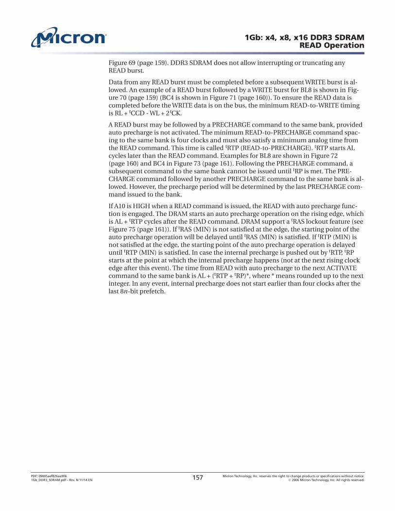
Figure 69 (page 159). DDR3 SDRAM does not allow interrupting or truncating anyREAD burst.
Data from any READ burst must be completed before a subsequent WRITE burst is al-lowed. An example of a READ burst followed by a WRITE burst for BL8 is shown in Fig-ure 70 (page 159) (BC4 is shown in Figure 71 (page 160)). To ensure the READ data iscompleted before the WRITE data is on the bus, the minimum READ-to-WRITE timingis RL + tCCD - WL + 2tCK.
A READ burst may be followed by a PRECHARGE command to the same bank, providedauto precharge is not activated. The minimum READ-to-PRECHARGE command spac-ing to the same bank is four clocks and must also satisfy a minimum analog time fromthe READ command. This time is called tRTP (READ-to-PRECHARGE). tRTP starts ALcycles later than the READ command. Examples for BL8 are shown in Figure 72(page 160) and BC4 in Figure 73 (page 161). Following the PRECHARGE command, asubsequent command to the same bank cannot be issued until tRP is met. The PRE-CHARGE command followed by another PRECHARGE command to the same bank is al-lowed. However, the precharge period will be determined by the last PRECHARGE com-mand issued to the bank.
If A10 is HIGH when a READ command is issued, the READ with auto precharge func-tion is engaged. The DRAM starts an auto precharge operation on the rising edge, whichis AL + tRTP cycles after the READ command. DRAM support a tRAS lockout feature (seeFigure 75 (page 161)). If tRAS (MIN) is not satisfied at the edge, the starting point of theauto precharge operation will be delayed until tRAS (MIN) is satisfied. If tRTP (MIN) isnot satisfied at the edge, the starting point of the auto precharge operation is delayeduntil tRTP (MIN) is satisfied. In case the internal precharge is pushed out by tRTP, tRPstarts at the point at which the internal precharge happens (not at the next rising clockedge after this event). The time from READ with auto precharge to the next ACTIVATEcommand to the same bank is AL + (tRTP + tRP)*, where * means rounded up to the nextinteger. In any event, internal precharge does not start earlier than four clocks after thelast 8n-bit prefetch.
1Gb: x4, x8, x16 DDR3 SDRAMREAD Operation
PDF: 09005aef826aa9061Gb_DDR3_SDRAM.pdf - Rev. N 11/14 EN 157 Micron Technology, Inc. reserves the right to change products or specifications without notice.
© 2006 Micron Technology, Inc. All rights reserved.
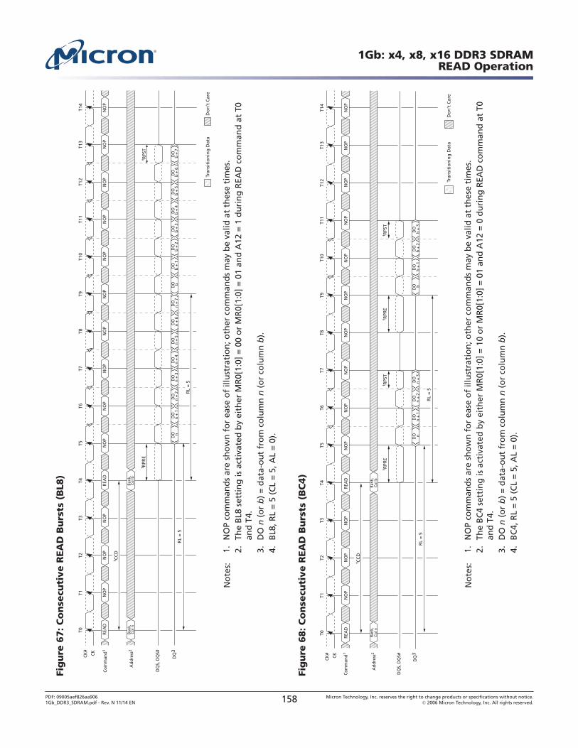
Fig
ure
67
: C
on
secu
tive R
EA
D B
urs
ts (
BL8
)
T0T1
T2T3
T4T5
T6T7
T8T9
T10
T11
Do
n’t
Car
eTr
ansi
tio
nin
g D
ata
T12
T13
T14
t RPS
T
NO
PRE
AD
REA
DN
OP
NO
PN
OP
NO
PN
OP
NO
PN
OP
NO
PN
OP
NO
PN
OP
NO
P
CKCK#
Com
man
d1
DQ
3
DQ
S, D
QS#
Bank
,Co
l nBa
nk,
Col b
Add
ress
2
RL
= 5
t RPR
E
t CC
D
RL
= 5
DO
n +
3D
O n
+ 2
DO
n +
1D
O nD
O n
+ 7
DO
n +
6D
O n
+ 5
DO
n
+ 4
DO
b +
3D
O b
+ 2
DO
b +
1D
O bD
O b
+ 7
DO
b +
6D
O b
+ 5
DO
b
+ 4
No
tes:
1.N
OP
com
man
ds
are
sho
wn
fo
r ea
se o
f ill
ust
rati
on
; oth
er c
om
man
ds
may
be
valid
at
thes
e ti
mes
.2.
The
BL8
set
tin
g is
act
ivat
ed b
y ei
ther
MR
0[1:
0] =
00
or
MR
0[1:
0] =
01
and
A12
= 1
du
rin
g R
EAD
co
mm
and
at
T0an
d T
4.3.
DO
n (
or
b)
= d
ata-
ou
t fr
om
co
lum
n n
(o
r co
lum
n b
).4.
BL8
, RL
= 5
(C
L =
5, A
L =
0).
Fig
ure
68
: C
on
secu
tive R
EA
D B
urs
ts (
BC
4)
NO
P
CKCK#
Com
man
d1
DQ
3
DQ
S, D
QS#
T0T1
T2T3
T4T5
T6T7
T8T9
Add
ress
2
T10
T11
Do
n’t
Car
eTr
ansi
tio
nin
g D
ata
T12
T13
T14
REA
DRE
AD
NO
PN
OP
NO
PN
OP
NO
PN
OP
NO
PN
OP
NO
PN
OP
NO
PN
OP
Bank
,Co
l nBa
nk,
Col b
t RPS
Tt R
PRE
t RPS
Tt R
PRE
RL
= 5
DO
n +
3D
O n
+ 2
DO
n +
1D
O nD
O b
+ 3
DO
b +
2D
O b
+ 1
DO b
RL
= 5
t CC
D
No
tes:
1.N
OP
com
man
ds
are
sho
wn
fo
r ea
se o
f ill
ust
rati
on
; oth
er c
om
man
ds
may
be
valid
at
thes
e ti
mes
.2.
The
BC
4 se
ttin
g is
act
ivat
ed b
y ei
ther
MR
0[1:
0] =
10
or
MR
0[1:
0] =
01
and
A12
= 0
du
rin
g R
EAD
co
mm
and
at
T0an
d T
4.3.
DO
n (
or
b)
= d
ata-
ou
t fr
om
co
lum
n n
(o
r co
lum
n b
).4.
BC
4, R
L =
5 (
CL
= 5
, AL
= 0
).
1Gb: x4, x8, x16 DDR3 SDRAMREAD Operation
PDF: 09005aef826aa9061Gb_DDR3_SDRAM.pdf - Rev. N 11/14 EN 158 Micron Technology, Inc. reserves the right to change products or specifications without notice.
© 2006 Micron Technology, Inc. All rights reserved.
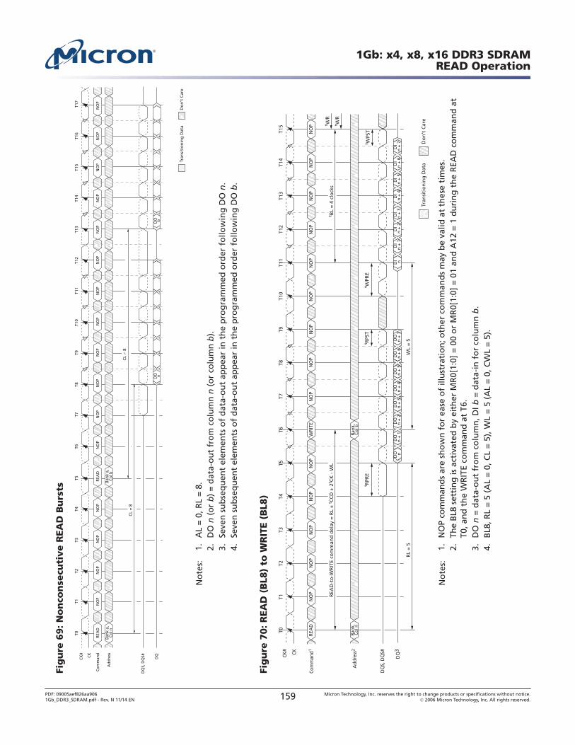
Fig
ure
69
: N
on
con
secu
tive R
EA
D B
urs
ts
Do
n’t
Car
eTr
ansi
tio
nin
g D
ata
T0T1
T2T3
T4T5
T6T7
T8T9
T10
T11
T12
T13
T14
T15
T16
T17
DQ
S, D
QS#
Com
man
dN
OP
NO
PN
OP
NO
PN
OP
NO
PN
OP
NO
PN
OP
NO
PN
OP
NO
PN
OP
NO
PN
OP
REA
DN
OP
REA
D
Add
ress
Bank
a,
Col n
Bank
a,
Col b
CKCK#
DQ
DO n
DO b
CL
= 8
C
L =
8
No
tes:
1.A
L =
0, R
L =
8.
2.D
O n
(o
r b
) =
dat
a-o
ut
fro
m c
olu
mn
n (
or
colu
mn
b).
3.Se
ven
su
bse
qu
ent
elem
ents
of
dat
a-o
ut
app
ear
in t
he
pro
gra
mm
ed o
rder
fo
llow
ing
DO
n.
4.Se
ven
su
bse
qu
ent
elem
ents
of
dat
a-o
ut
app
ear
in t
he
pro
gra
mm
ed o
rder
fo
llow
ing
DO
b.
Fig
ure
70
: R
EA
D (
BL8
) to
WR
ITE (
BL8
)
Do
n’t
Car
eTr
ansi
tio
nin
g D
ata
T0T1
T2T3
T4T5
T6T7
T8T9
T10
T11
T12
T13
T14
T15
CKCK#
Com
man
d1N
OP
NO
PN
OP
NO
PN
OP
WRI
TEN
OP
NO
PN
OP
NO
PN
OP
NO
PN
OP
NO
PN
OP
t WPS
Tt R
PRE
t WPR
Et R
PST
DQ
S, D
QS#
DQ
3
WL
= 5
t WR
t WR
REA
D
DO n
DO
n +
1D
O n
+ 2
DO
n +
3D
O n
+ 4
DO
n +
5D
O n
+ 6
DO
n +
7D
I n
DI
n +
1D
I n
+ 2
DI
n +
3D
I n
+ 4
DI
n +
5D
I n
+ 6
DI
n +
7
REA
D-t
o-W
RIT
E co
mm
and
del
ay =
RL
+ t C
CD
+ 2
t CK
- W
Lt B
L =
4 c
lock
s
Add
ress
2Ba
nk,
Col b
Bank
,Co
l n
RL
= 5
No
tes:
1.N
OP
com
man
ds
are
sho
wn
fo
r ea
se o
f ill
ust
rati
on
; oth
er c
om
man
ds
may
be
valid
at
thes
e ti
mes
.2.
The
BL8
set
tin
g is
act
ivat
ed b
y ei
ther
MR
0[1:
0] =
00
or
MR
0[1:
0] =
01
and
A12
= 1
du
rin
g t
he
REA
D c
om
man
d a
tT0
, an
d t
he
WR
ITE
com
man
d a
t T6
.3.
DO
n =
dat
a-o
ut
fro
m c
olu
mn
, DI b
= d
ata-
in f
or
colu
mn
b.
4.B
L8, R
L =
5 (
AL
= 0
, CL
= 5
), W
L =
5 (
AL
= 0
, CW
L =
5).
1Gb: x4, x8, x16 DDR3 SDRAMREAD Operation
PDF: 09005aef826aa9061Gb_DDR3_SDRAM.pdf - Rev. N 11/14 EN 159 Micron Technology, Inc. reserves the right to change products or specifications without notice.
© 2006 Micron Technology, Inc. All rights reserved.
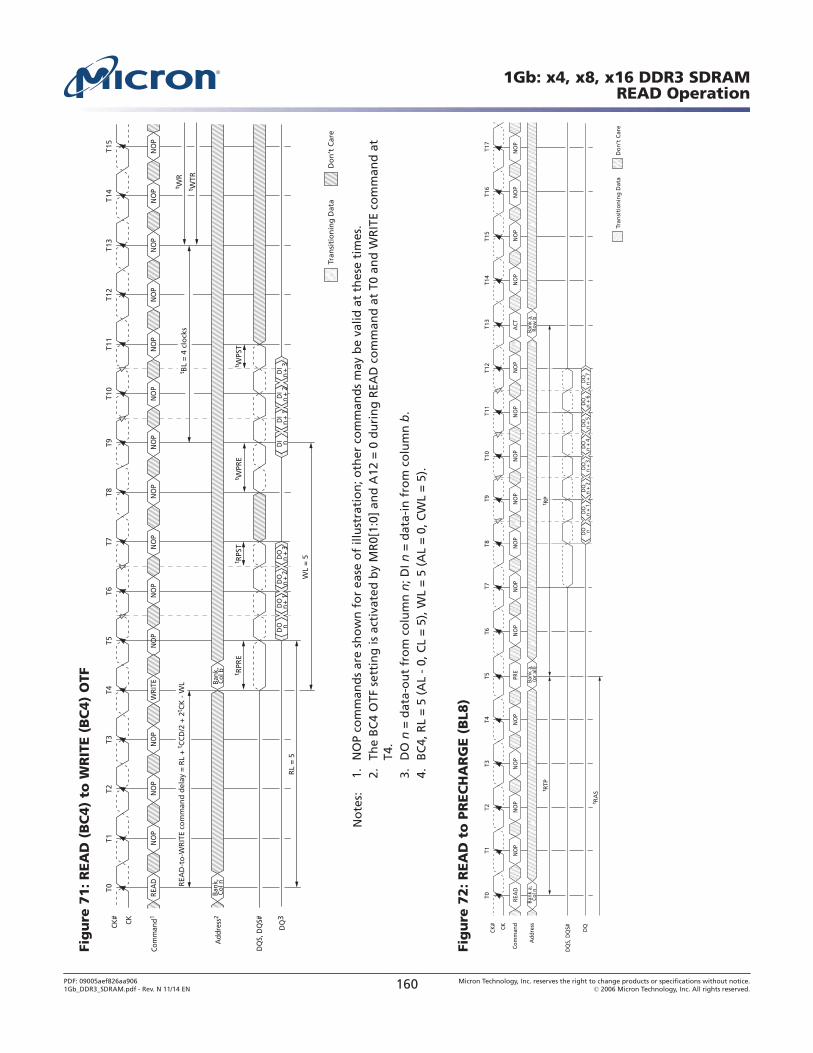
Fig
ure
71
: R
EA
D (
BC
4)
to W
RIT
E (
BC
4)
OTF
Do
n’t
Car
eTr
ansi
tio
nin
g D
ata
T0T1
T2T3
T4T5
T6T7
T8T9
T10
T11
T12
T13
T14
T15
CKCK#
Add
ress
2
Com
man
d1
t WPS
Tt W
PRE
t RPS
T
DQ
S, D
QS#
DQ
3
WL
= 5
t WR
t WTR
t BL
= 4
clo
cks
t RPR
E
RL
= 5
REA
D-t
o-W
RIT
E co
mm
and
del
ay =
RL
+ t C
CD
/2 +
2t C
K -
WL
REA
D
DO n
DO
n +
1D
On
+ 2
DO
n +
3D
I nD
In
+ 1
DI
n +
2D
In
+ 3
Bank
,Co
l bBa
nk,
Col n
NO
PN
OP
NO
PW
RITE
NO
PN
OP
NO
PN
OP
NO
PN
OP
NO
PN
OP
NO
PN
OP
NO
P
No
tes:
1.N
OP
com
man
ds
are
sho
wn
fo
r ea
se o
f ill
ust
rati
on
; oth
er c
om
man
ds
may
be
valid
at
thes
e ti
mes
.2.
The
BC
4 O
TF s
etti
ng
is a
ctiv
ated
by
MR
0[1:
0] a
nd
A12
= 0
du
rin
g R
EAD
co
mm
and
at
T0 a
nd
WR
ITE
com
man
d a
tT4
.3.
DO
n =
dat
a-o
ut
fro
m c
olu
mn
n; D
I n =
dat
a-in
fro
m c
olu
mn
b.
4.B
C4,
RL
= 5
(A
L -
0, C
L =
5),
WL
= 5
(A
L =
0, C
WL
= 5
).
Fig
ure
72
: R
EA
D t
o P
REC
HA
RG
E (
BL8
)
t RA
St RTP
CKCK#
Com
man
dN
OP
NO
PN
OP
NO
P
Add
ress
DQ
DQ
S, D
QS#
Do
n’t
Car
eTr
ansi
tio
nin
g D
ata
NO
PN
OP
NO
PN
OP
NO
PA
CTN
OP
NO
PN
OP
NO
P
T0T1
T2T3
T4T5
T6T7
T8T9
T10
T11
T12
T13
T14
T15
T16
T17
NO
PRE
AD
Bank
a,
Col n
NO
PPR
E
Bank
a,
(or
all)
Bank
a,
Row
b
t RP
DO n
DO
n +
1D
On
+ 2
DO
n +
3D
On
+ 4
DO
n +
5D
On
+ 6
DO
n +
7
1Gb: x4, x8, x16 DDR3 SDRAMREAD Operation
PDF: 09005aef826aa9061Gb_DDR3_SDRAM.pdf - Rev. N 11/14 EN 160 Micron Technology, Inc. reserves the right to change products or specifications without notice.
© 2006 Micron Technology, Inc. All rights reserved.
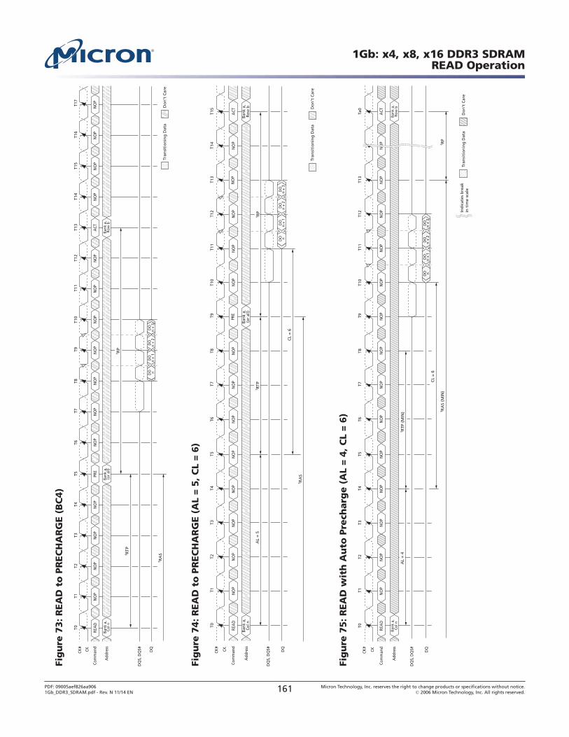
Fig
ure
73
: R
EA
D t
o P
REC
HA
RG
E (
BC
4)
CKCK#
Do
n’t
Car
eTr
ansi
tio
nin
g D
ata
T0T1
T2T3
T4T5
T6T7
T8T9
T10
T11
T12
T13
T14
T15
T16
T17
Com
man
dN
OP
NO
PN
OP
NO
PN
OP
NO
PN
OP
NO
PN
OP
ACT
NO
PN
OP
NO
PN
OP
NO
PRE
AD
NO
PPR
E
Add
ress
Bank
a,
Col n
Bank
a,
(or
all)
Bank
a,
Row
b
t RP
t RTP
DQ
S, D
QS# DQ
DO n
DO
n +
1D
On
+ 2
DO
n +
3
t RA
S
Fig
ure
74
: R
EA
D t
o P
REC
HA
RG
E (
AL
= 5, C
L =
6)
CKCK#
Com
man
dN
OP
NO
PN
OP
NO
P
Add
ress
DQ
DQ
S, D
QS#
Do
n’t
Car
eTr
ansi
tio
nin
g D
ata
NO
PN
OP
NO
PN
OP
NO
P
T0T1
T2T3
T4T5
T6T7
T8T9
T10
T11
T12
T13
T14
T15
NO
PRE
AD
Bank
a,
Col n
NO
PPR
E
Bank
a,
(or
all)
ACT
Bank
a,
Row
b
NO
PN
OP
t RA
S
CL
= 6
AL
= 5
t RTP
t RP
DO
n +
3D
On
+ 2
DO n
DO
n +
1
Fig
ure
75
: R
EA
D w
ith
Au
to P
rech
arg
e (
AL
= 4, C
L =
6)
CKCK#
Com
man
dN
OP
NO
PN
OP
NO
P
Add
ress
DQ
DQ
S, D
QS#
Do
n’t
Car
eTr
ansi
tio
nin
g D
ata
NO
PN
OP
NO
PN
OP
NO
P
T0T1
T2T3
T4T5
T6T7
T8T9
T10
T11
T12
T13
Ta0
t RTP
(M
IN)
NO
PRE
AD
NO
P
AL
= 4
NO
PN
OP
CL
= 6
NO
P
t RA
S (M
IN)
ACT
Ind
icat
es b
reak
in t
ime
scal
e
t RP
Bank
a,
Col n
Bank
a,
Row
b
DO n
DO
n +
1D
On
+ 2
DO
n +
3
1Gb: x4, x8, x16 DDR3 SDRAMREAD Operation
PDF: 09005aef826aa9061Gb_DDR3_SDRAM.pdf - Rev. N 11/14 EN 161 Micron Technology, Inc. reserves the right to change products or specifications without notice.
© 2006 Micron Technology, Inc. All rights reserved.
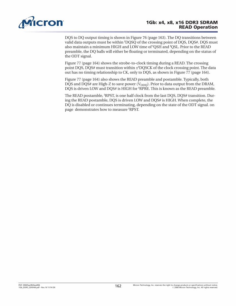
DQS to DQ output timing is shown in Figure 76 (page 163). The DQ transitions betweenvalid data outputs must be within tDQSQ of the crossing point of DQS, DQS#. DQS mustalso maintain a minimum HIGH and LOW time of tQSH and tQSL. Prior to the READpreamble, the DQ balls will either be floating or terminated, depending on the status ofthe ODT signal.
Figure 77 (page 164) shows the strobe-to-clock timing during a READ. The crossingpoint DQS, DQS# must transition within ±tDQSCK of the clock crossing point. The dataout has no timing relationship to CK, only to DQS, as shown in Figure 77 (page 164).
Figure 77 (page 164) also shows the READ preamble and postamble. Typically, bothDQS and DQS# are High-Z to save power (VDDQ). Prior to data output from the DRAM,DQS is driven LOW and DQS# is HIGH for tRPRE. This is known as the READ preamble.
The READ postamble, tRPST, is one half clock from the last DQS, DQS# transition. Dur-ing the READ postamble, DQS is driven LOW and DQS# is HIGH. When complete, theDQ is disabled or continues terminating, depending on the state of the ODT signal. onpage demonstrates how to measure tRPST.
1Gb: x4, x8, x16 DDR3 SDRAMREAD Operation
PDF: 09005aef826aa9061Gb_DDR3_SDRAM.pdf - Rev. N 11/14 EN 162 Micron Technology, Inc. reserves the right to change products or specifications without notice.
© 2006 Micron Technology, Inc. All rights reserved.
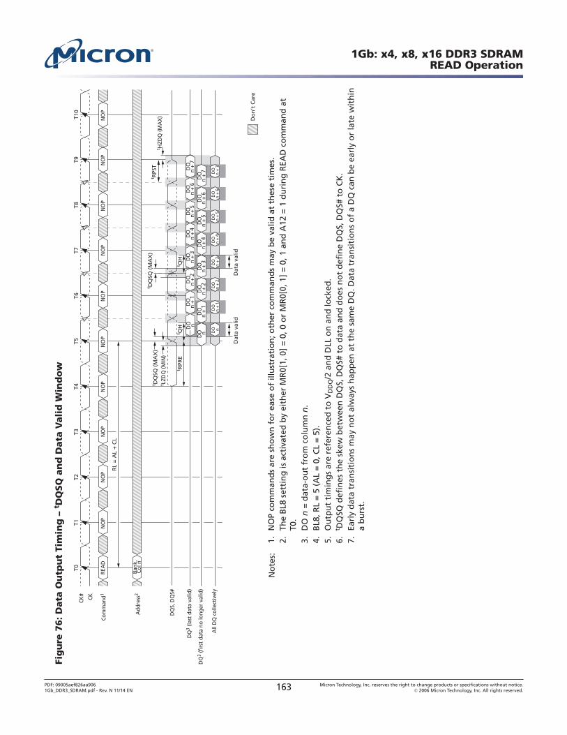
Fig
ure
76
: D
ata
Ou
tpu
t Ti
min
g –
tD
QSQ
an
d D
ata
Vali
d W
ind
ow
T0T1
T2T3
T4T5
T6T7
T8T9
T10
Bank
,Co
l n
t RPS
T
NO
PRE
AD
NO
PN
OP
NO
PN
OP
NO
PN
OP
NO
PN
OP
NO
P
CKCK#
Com
man
d1
Add
ress
2
t DQ
SQ (
MA
X)
DQ
S, D
QS#
DQ
3 (la
st d
ata
valid
)
DQ
3 (f
irst
dat
a no
long
er v
alid
)
All
DQ
col
lect
ivel
y
DO n
DO
n +
3D
On
+ 2
DO
n +
1D
On
+ 7
DO
n +
6D
On
+ 5
DO
n +
4D
On
+ 2
DO
n +
1D
On
+ 7
DO
n +
6D
On
+ 5
DO
n +
4
DO
n +
3D
O n
+ 2
DO
n +
1D
O nD
O n
+ 7
DO
n +
6D
O n
+ 5
DO n
DO
n +
3
t RPR
E
Do
n’t
Car
e
Dat
a va
lidD
ata
valid
t QH
t QH
t HZD
Q (M
AX
)
DO
n
+ 4
RL
= A
L +
CL
t DQ
SQ (
MA
X)
t LZD
Q (M
IN)
No
tes:
1.N
OP
com
man
ds
are
sho
wn
fo
r ea
se o
f ill
ust
rati
on
; oth
er c
om
man
ds
may
be
valid
at
thes
e ti
mes
.2.
The
BL8
set
tin
g is
act
ivat
ed b
y ei
ther
MR
0[1,
0]
= 0
, 0 o
r M
R0[
0, 1
] =
0, 1
an
d A
12 =
1 d
uri
ng
REA
D c
om
man
d a
tT0
.3.
DO
n =
dat
a-o
ut
fro
m c
olu
mn
n.
4.B
L8, R
L =
5 (
AL
= 0
, CL
= 5
).5.
Ou
tpu
t ti
min
gs
are
refe
ren
ced
to
VD
DQ
/2 a
nd
DLL
on
an
d lo
cked
.6.
t DQ
SQ d
efin
es t
he
skew
bet
wee
n D
QS,
DQ
S# t
o d
ata
and
do
es n
ot
def
ine
DQ
S, D
QS#
to
CK
.7.
Earl
y d
ata
tran
siti
on
s m
ay n
ot
alw
ays
hap
pen
at
the
sam
e D
Q. D
ata
tran
siti
on
s o
f a
DQ
can
be
earl
y o
r la
te w
ith
ina
bu
rst.
1Gb: x4, x8, x16 DDR3 SDRAMREAD Operation
PDF: 09005aef826aa9061Gb_DDR3_SDRAM.pdf - Rev. N 11/14 EN 163 Micron Technology, Inc. reserves the right to change products or specifications without notice.
© 2006 Micron Technology, Inc. All rights reserved.
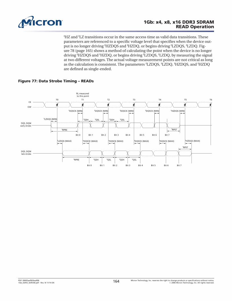
tHZ and tLZ transitions occur in the same access time as valid data transitions. Theseparameters are referenced to a specific voltage level that specifies when the device out-put is no longer driving tHZDQS and tHZDQ, or begins driving tLZDQS, tLZDQ. Fig-ure 78 (page 165) shows a method of calculating the point when the device is no longerdriving tHZDQS and tHZDQ, or begins driving tLZDQS, tLZDQ, by measuring the signalat two different voltages. The actual voltage measurement points are not critical as longas the calculation is consistent. The parameters tLZDQS, tLZDQ, tHZDQS, and tHZDQare defined as single-ended.
Figure 77: Data Strobe Timing – READs
RL measuredto this point
DQS, DQS#early strobe
CK
tLZDQS (MIN)
tHZDQS (MIN)
DQS, DQS#late strobe
tLZDQS (MAX) tHZDQS (MAX)tDQSCK (MAX) tDQSCK (MAX) tDQSCK (MAX) tDQSCK (MAX)
tDQSCK (MIN) tDQSCK (MIN) tDQSCK (MIN) tDQSCK (MIN)
CK#
tRPRE
tQSH tQSHtQSL tQSL
tQSL tQSLtQSH tQSH
Bit 0 Bit 1 Bit 2 Bit 7
tRPRE
Bit 0 Bit 1 Bit 2 Bit 7Bit 6Bit 3 Bit 4 Bit 5
Bit 6Bit 4Bit 3 Bit 5
tRPST
tRPST
T0 T1 T2 T3 T4 T5 T6
1Gb: x4, x8, x16 DDR3 SDRAMREAD Operation
PDF: 09005aef826aa9061Gb_DDR3_SDRAM.pdf - Rev. N 11/14 EN 164 Micron Technology, Inc. reserves the right to change products or specifications without notice.
© 2006 Micron Technology, Inc. All rights reserved.
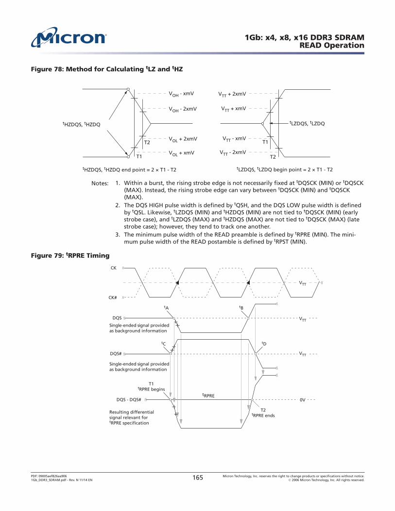
Figure 78: Method for Calculating tLZ and tHZ
tHZDQS, tHZDQ
tHZDQS, tHZDQ end point = 2 × T1 - T2
VOH - xmV
VTT - xmV
VOL + xmV
VTT + xmVVOH - 2xmV
VTT - 2xmV
VOL + 2xmV
VTT + 2xmV
tLZDQS, tLZDQ
tLZDQS, tLZDQ begin point = 2 × T1 - T2
T1
T1T2
T2
Notes: 1. Within a burst, the rising strobe edge is not necessarily fixed at tDQSCK (MIN) or tDQSCK(MAX). Instead, the rising strobe edge can vary between tDQSCK (MIN) and tDQSCK(MAX).
2. The DQS HIGH pulse width is defined by tQSH, and the DQS LOW pulse width is definedby tQSL. Likewise, tLZDQS (MIN) and tHZDQS (MIN) are not tied to tDQSCK (MIN) (earlystrobe case), and tLZDQS (MAX) and tHZDQS (MAX) are not tied to tDQSCK (MAX) (latestrobe case); however, they tend to track one another.
3. The minimum pulse width of the READ preamble is defined by tRPRE (MIN). The mini-mum pulse width of the READ postamble is defined by tRPST (MIN).
Figure 79: tRPRE Timing
tRPREDQS - DQS#
DQS
DQS#
T1tRPRE begins
T2tRPRE ends
CK
CK#
VTT
Resulting differential signal relevant for tRPRE specification
tC
tA tB
tD
Single-ended signal providedas background information
0V
Single-ended signal providedas background information
VTT
VTT
1Gb: x4, x8, x16 DDR3 SDRAMREAD Operation
PDF: 09005aef826aa9061Gb_DDR3_SDRAM.pdf - Rev. N 11/14 EN 165 Micron Technology, Inc. reserves the right to change products or specifications without notice.
© 2006 Micron Technology, Inc. All rights reserved.
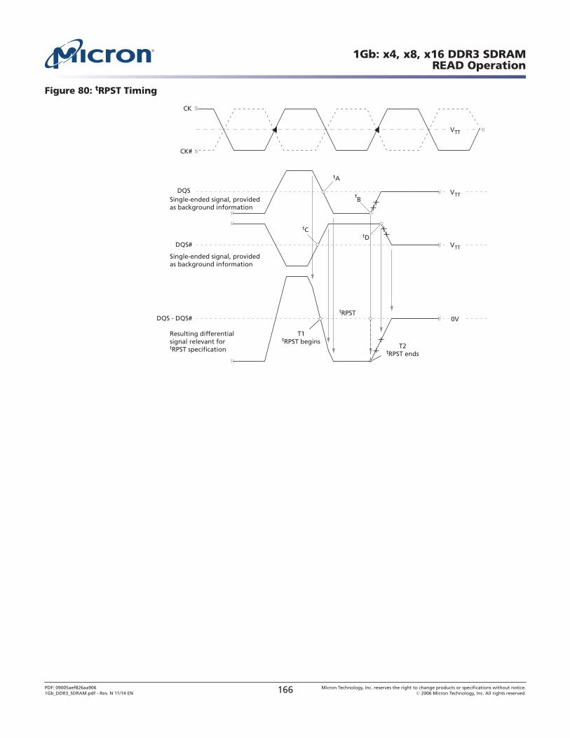
Figure 80: tRPST Timing
tRPSTDQS - DQS#
DQS
DQS#
T1tRPST begins
T2tRPST ends
Resulting differential signal relevant for tRPST specification
CK
CK#
VTT
tC
tA
tB
tD
Single-ended signal, providedas background information
Single-ended signal, providedas background information
0V
VTT
VTT
1Gb: x4, x8, x16 DDR3 SDRAMREAD Operation
PDF: 09005aef826aa9061Gb_DDR3_SDRAM.pdf - Rev. N 11/14 EN 166 Micron Technology, Inc. reserves the right to change products or specifications without notice.
© 2006 Micron Technology, Inc. All rights reserved.
WRITE OperationWRITE bursts are initiated with a WRITE command. The starting column and bank ad-dresses are provided with the WRITE command, and auto precharge is either enabled ordisabled for that access. If auto precharge is selected, the row being accessed is pre-charged at the end of the WRITE burst. If auto precharge is not selected, the row willremain open for subsequent accesses. After a WRITE command has been issued, theWRITE burst may not be interrupted. For the generic WRITE commands used in Fig-ure 83 (page 169) through Figure 91 (page 174), auto precharge is disabled.
During WRITE bursts, the first valid data-in element is registered on a rising edge ofDQS following the WRITE latency (WL) clocks later and subsequent data elements willbe registered on successive edges of DQS. WRITE latency (WL) is defined as the sum ofposted CAS additive latency (AL) and CAS WRITE latency (CWL): WL = AL + CWL. Thevalues of AL and CWL are programmed in the MR0 and MR2 registers, respectively. Priorto the first valid DQS edge, a full cycle is needed (including a dummy crossover of DQS,DQS#) and specified as the WRITE preamble shown in Figure 83 (page 169). The halfcycle on DQS following the last data-in element is known as the WRITE postamble.
The time between the WRITE command and the first valid edge of DQS is WL clocks±tDQSS. Figure 84 (page 170) through Figure 91 (page 174) show the nominal casewhere tDQSS = 0ns; however, Figure 83 (page 169) includes tDQSS (MIN) and tDQSS(MAX) cases.
Data may be masked from completing a WRITE using data mask. The data mask occurson the DM ball aligned to the WRITE data. If DM is LOW, the WRITE completes normal-ly. If DM is HIGH, that bit of data is masked.
Upon completion of a burst, assuming no other commands have been initiated, the DQwill remain High-Z, and any additional input data will be ignored.
Data for any WRITE burst may be concatenated with a subsequent WRITE command toprovide a continuous flow of input data. The new WRITE command can be tCCD clocksfollowing the previous WRITE command. The first data element from the new burst isapplied after the last element of a completed burst. Figure 84 (page 170) and Figure 85(page 170) show concatenated bursts. An example of nonconsecutive WRITEs is shownin Figure 86 (page 171).
Data for any WRITE burst may be followed by a subsequent READ command after tWTRhas been met (see Figure 87 (page 171), Figure 88 (page 172), and Figure 89(page 173)).
Data for any WRITE burst may be followed by a subsequent PRECHARGE command,providing tWR has been met, as shown in Figure 90 (page 174) and Figure 91(page 174).
Both tWTR and tWR starting time may vary, depending on the mode register settings(fixed BC4, BL8 versus OTF).
1Gb: x4, x8, x16 DDR3 SDRAMWRITE Operation
PDF: 09005aef826aa9061Gb_DDR3_SDRAM.pdf - Rev. N 11/14 EN 167 Micron Technology, Inc. reserves the right to change products or specifications without notice.
© 2006 Micron Technology, Inc. All rights reserved.
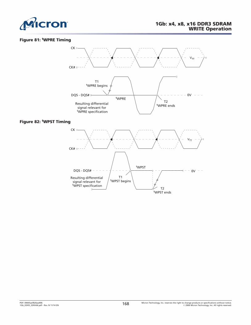
Figure 81: tWPRE Timing
DQS - DQS#
T1tWPRE begins
T2tWPRE ends
tWPREResulting differential
signal relevant for tWPRE specification
0V
CK
CK#
VTT
Figure 82: tWPST Timing
tWPSTDQS - DQS#
T1tWPST begins
T2tWPST ends
Resulting differential signal relevant for tWPST specification
0V
CK
CK#
VTT
1Gb: x4, x8, x16 DDR3 SDRAMWRITE Operation
PDF: 09005aef826aa9061Gb_DDR3_SDRAM.pdf - Rev. N 11/14 EN 168 Micron Technology, Inc. reserves the right to change products or specifications without notice.
© 2006 Micron Technology, Inc. All rights reserved.
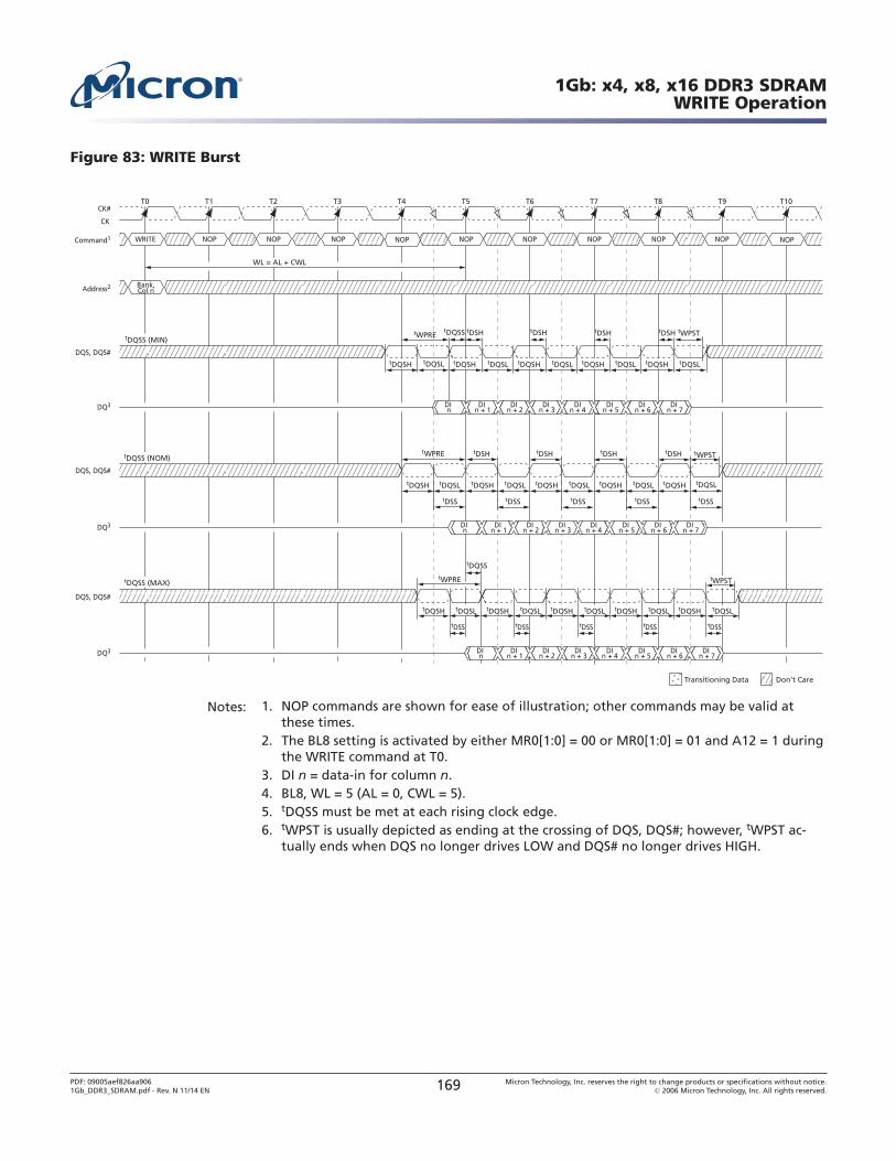
Figure 83: WRITE Burst
DIn + 3
DI n + 2
DIn + 1
DIn
T0 T1 T2 T3 T4 T5 T6 T7 T8 T9 T10
Don’t CareTransitioning Data
DIn + 7
DI n + 6
DIn + 5
DIn + 4
Bank,Col n
NOPWRITE NOPNOP NOP NOP NOP NOP NOP NOP NOP
CK
CK#
Command1
DQ3
DQS, DQS#
Address2
tWPST
tWPRE tWPST
tDQSL
DQ3
DQ3
tWPST
DQS, DQS#
DQS, DQS#
tDQSL
tWPRE
tDQSS
tDQSS tDSH tDSH tDSH tDSH
tDSS tDSS tDSS tDSS tDSS
tDSS tDSS tDSS tDSS tDSS
tDSH tDSH tDSH tDSH
tDQSLtDQSH tDQSLtDQSH tDQSLtDQSH tDQSH tDQSL
tDQSL
tDQSL
tDQSLtDQSHtDQSH
tDQSH
tDQSH
tDQSLtDQSH tDQSLtDQSH tDQSH
tDQSLtDQSH tDQSLtDQSH tDQSLtDQSH tDQSH
WL = AL + CWL
tDQSS (MIN)
tDQSS (NOM)
tDQSS (MAX)
tDQSL
tWPRE
DI n + 3
DI n + 2
DI n + 1
DI n
DIn + 7
DI n + 6
DI n + 5
DIn + 4
DIn + 3
DIn + 2
DIn + 1
DI n
DIn + 7
DIn + 6
DIn + 5
DIn + 4
Notes: 1. NOP commands are shown for ease of illustration; other commands may be valid atthese times.
2. The BL8 setting is activated by either MR0[1:0] = 00 or MR0[1:0] = 01 and A12 = 1 duringthe WRITE command at T0.
3. DI n = data-in for column n.4. BL8, WL = 5 (AL = 0, CWL = 5).5. tDQSS must be met at each rising clock edge.6. tWPST is usually depicted as ending at the crossing of DQS, DQS#; however, tWPST ac-
tually ends when DQS no longer drives LOW and DQS# no longer drives HIGH.
1Gb: x4, x8, x16 DDR3 SDRAMWRITE Operation
PDF: 09005aef826aa9061Gb_DDR3_SDRAM.pdf - Rev. N 11/14 EN 169 Micron Technology, Inc. reserves the right to change products or specifications without notice.
© 2006 Micron Technology, Inc. All rights reserved.
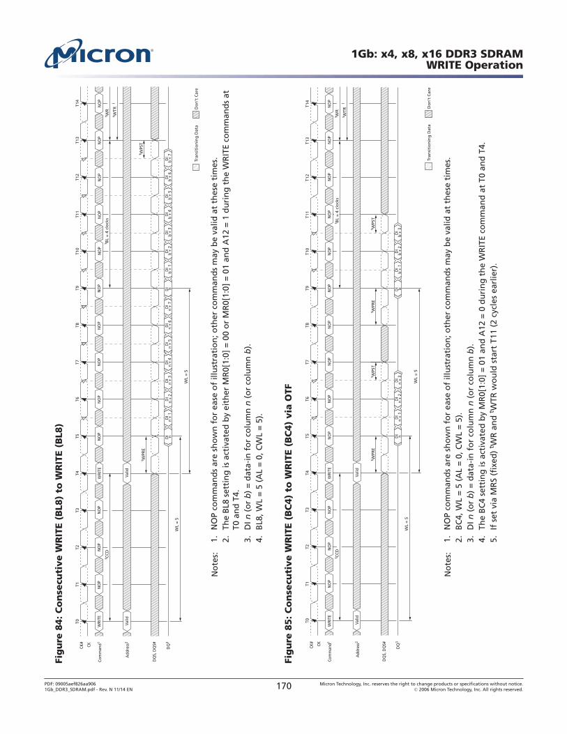
Fig
ure
84
: C
on
secu
tive W
RIT
E (
BL8
) to
WR
ITE (
BL8
)
WL
= 5
WL
= 5
T0T1
T2T3
T4T5
T6T7
T8T9
t CC
D
t WPR
E
T10
T11
Do
n’t
Car
eTr
ansi
tio
nin
g D
ata
T12
T13
T14
Valid
Valid
NO
PW
RITE
WRI
TEN
OP
NO
PN
OP
NO
PN
OP
NO
PN
OP
NO
PN
OP
NO
PN
OP
NO
P
CKCK#
Com
man
d1
DQ
3
DQ
S, D
QS#
Add
ress
2
t WPS
T
t WR
t WTR
t BL
= 4
clo
cks
DI
n +
3D
I n
+ 2
DI
n +
1D
I n
DI
n +
7D
I n
+ 6
DI
n +
5D
In
+ 4
DI
b +
3D
I b
+ 2
DI
b +
1D
I b
DI
b +
7D
I b
+ 6
DI
b +
5D
Ib
+ 4
No
tes:
1.N
OP
com
man
ds
are
sho
wn
fo
r ea
se o
f ill
ust
rati
on
; oth
er c
om
man
ds
may
be
valid
at
thes
e ti
mes
.2.
The
BL8
set
tin
g is
act
ivat
ed b
y ei
ther
MR
0[1:
0] =
00
or
MR
0[1:
0] =
01
and
A12
= 1
du
rin
g t
he
WR
ITE
com
man
ds
atT0
an
d T
4.3.
DI n
(o
r b
) =
dat
a-in
fo
r co
lum
n n
(o
r co
lum
n b
).4.
BL8
, WL
= 5
(A
L =
0, C
WL
= 5
).
Fig
ure
85
: C
on
secu
tive W
RIT
E (
BC
4)
to W
RIT
E (
BC
4)
via
OTF
WL
= 5
WL
= 5
T0T1
T2T3
T4T5
T6T7
T8T9
t CC
D
t WPR
E
T10
T11
Do
n’t
Car
eTr
ansi
tio
nin
g D
ata
T12
T13
T14
Valid
Valid
NO
PW
RITE
WRI
TEN
OP
NO
PN
OP
NO
PN
OP
NO
PN
OP
NO
PN
OP
NO
PN
OP
NO
P
CKCK#
Com
man
d1
DQ
3
DQ
S, D
QS#
Add
ress
2
t WPS
T
t WR
t WTR
t WPS
Tt W
PRE
DI
n +
3D
I n
+ 2
DI
n +
1D
I nD
I b
+ 3
DI
b +
2D
I b
+ 1
DI
b
t BL
= 4
clo
cks
No
tes:
1.N
OP
com
man
ds
are
sho
wn
fo
r ea
se o
f ill
ust
rati
on
; oth
er c
om
man
ds
may
be
valid
at
thes
e ti
mes
.2.
BC
4, W
L =
5 (
AL
= 0
, CW
L =
5).
3.D
I n (
or
b)
= d
ata-
in f
or
colu
mn
n (
or
colu
mn
b).
4.Th
e B
C4
sett
ing
is a
ctiv
ated
by
MR
0[1:
0] =
01
and
A12
= 0
du
rin
g t
he
WR
ITE
com
man
d a
t T0
an
d T
4.5.
If s
et v
ia M
RS
(fix
ed)
t WR
an
d t W
TR w
ou
ld s
tart
T11
(2
cycl
es e
arlie
r).
1Gb: x4, x8, x16 DDR3 SDRAMWRITE Operation
PDF: 09005aef826aa9061Gb_DDR3_SDRAM.pdf - Rev. N 11/14 EN 170 Micron Technology, Inc. reserves the right to change products or specifications without notice.
© 2006 Micron Technology, Inc. All rights reserved.
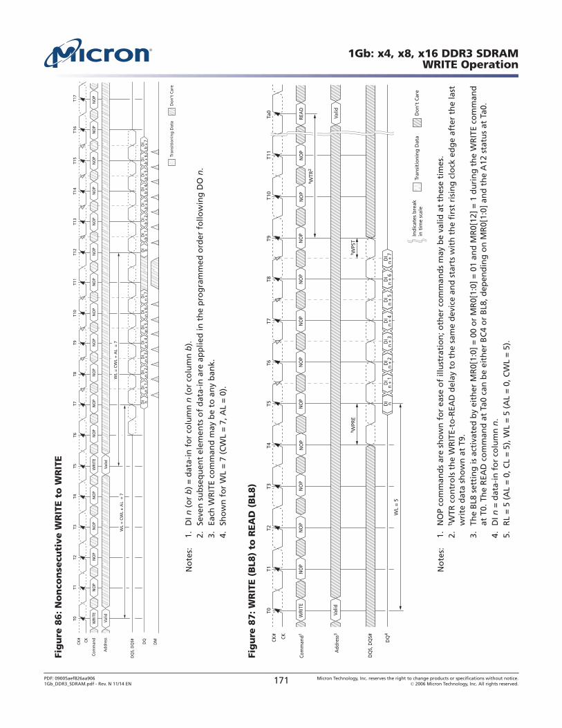
Fig
ure
86
: N
on
con
secu
tive W
RIT
E t
o W
RIT
E
CKCK#
Com
man
dN
OP
NO
PN
OP
Add
ress
DQ
DM
DQ
S, D
QS#
Tran
siti
on
ing
Dat
a
NO
PN
OP
NO
PN
OP
NO
PN
OP
NO
PN
OP
NO
PN
OP
T0T1
T2T3
T4T5
T6T7
T8T9
T10
T11
T12
T13
T14
T15
T16
T17
NO
PW
RITE
NO
PW
RITE
Valid
Valid
NO
P
DI n
DI
n +
1D
In
+ 2
DI
n +
3D
In
+ 4
DI
n +
5D
In
+ 6
Do
n't
Car
e
DI
n +
7D
I bD
Ib
+ 1
DI
b +
2D
Ib
+ 3
DI
b +
4D
Ib
+ 5
DI
b +
6D
Ib
+ 7
WL
= C
WL
+ A
L =
7W
L =
CW
L +
AL
= 7
No
tes:
1.D
I n (
or
b)
= d
ata-
in f
or
colu
mn
n (
or
colu
mn
b).
2.Se
ven
su
bse
qu
ent
elem
ents
of
dat
a-in
are
ap
plie
d in
th
e p
rog
ram
med
ord
er f
ollo
win
g D
O n
.3.
Each
WR
ITE
com
man
d m
ay b
e to
an
y b
ank.
4.Sh
ow
n f
or
WL
= 7
(C
WL
= 7
, AL
= 0
).
Fig
ure
87
: W
RIT
E (
BL8
) to
REA
D (
BL8
)
WL
= 5
T0T1
T2T3
T4T5
T6T7
T8T9
t WPR
E
T10
T11
Do
n’t
Car
eTr
ansi
tio
nin
g D
ata
Ta0
NO
PW
RITE
REA
D
Valid
Valid
NO
PN
OP
NO
PN
OP
NO
PN
OP
NO
PN
OP
NO
PN
OP
CKCK#
Com
man
d1
DQ
4
DQ
S, D
QS#
Add
ress
3
t WPS
T
t WTR
2
Ind
icat
es b
reak
in t
ime
scal
e
DI
n +
3D
In
+ 2
DI
n +
1D
I nD
In
+ 7
DI
n +
6D
In
+ 5
DI
n +
4
No
tes:
1.N
OP
com
man
ds
are
sho
wn
fo
r ea
se o
f ill
ust
rati
on
; oth
er c
om
man
ds
may
be
valid
at
thes
e ti
mes
.2.
t WTR
co
ntr
ols
th
e W
RIT
E-to
-REA
D d
elay
to
th
e sa
me
dev
ice
and
sta
rts
wit
h t
he
firs
t ri
sin
g c
lock
ed
ge
afte
r th
e la
stw
rite
dat
a sh
ow
n a
t T9
.3.
The
BL8
set
tin
g is
act
ivat
ed b
y ei
ther
MR
0[1:
0] =
00
or
MR
0[1:
0] =
01
and
MR
0[12
] =
1 d
uri
ng
th
e W
RIT
E co
mm
and
at T
0. T
he
REA
D c
om
man
d a
t Ta
0 ca
n b
e ei
ther
BC
4 o
r B
L8, d
epen
din
g o
n M
R0[
1:0]
an
d t
he
A12
sta
tus
at T
a0.
4.D
I n =
dat
a-in
fo
r co
lum
n n
.5.
RL
= 5
(A
L =
0, C
L =
5),
WL
= 5
(A
L =
0, C
WL
= 5
).
1Gb: x4, x8, x16 DDR3 SDRAMWRITE Operation
PDF: 09005aef826aa9061Gb_DDR3_SDRAM.pdf - Rev. N 11/14 EN 171 Micron Technology, Inc. reserves the right to change products or specifications without notice.
© 2006 Micron Technology, Inc. All rights reserved.
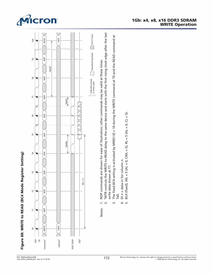
Fig
ure
88
: W
RIT
E t
o R
EA
D (
BC
4 M
od
e R
eg
iste
r Sett
ing
)
WL
= 5
T0T1
T2T3
T4T5
T6T7
T8T9
Ta0
Do
n’t
Car
eTr
ansi
tio
nin
g D
ata
NO
PW
RITE
Valid
REA
D
Valid
NO
PN
OP
NO
PN
OP
NO
PN
OP
NO
PN
OP
CKCK#
Com
man
d1
DQ
4
DQ
S, D
QS#
Add
ress
3
t WPS
T
t WTR
2
t WPR
E
Ind
icat
es b
reak
in t
ime
scal
e
DI
n +
3D
In
+ 2
DI
n +
1D
I n
No
tes:
1.N
OP
com
man
ds
are
sho
wn
fo
r ea
se o
f ill
ust
rati
on
; oth
er c
om
man
ds
may
be
valid
at
thes
e ti
mes
.2.
t WTR
co
ntr
ols
th
e W
RIT
E-to
-REA
D d
elay
to
th
e sa
me
dev
ice
and
sta
rts
wit
h t
he
firs
t ri
sin
g c
lock
ed
ge
afte
r th
e la
stw
rite
dat
a sh
ow
n a
t T7
.3.
The
fixe
d B
C4
sett
ing
is a
ctiv
ated
by
MR
0[1:
0] =
10
du
rin
g t
he
WR
ITE
com
man
d a
t T0
an
d t
he
REA
D c
om
man
d a
tTa
0.4.
DI n
= d
ata-
in f
or
colu
mn
n.
5.B
C4
(fix
ed),
WL
= 5
(A
L =
0, C
WL
= 5
), R
L =
5 (
AL
= 0
, CL
= 5
).
1Gb: x4, x8, x16 DDR3 SDRAMWRITE Operation
PDF: 09005aef826aa9061Gb_DDR3_SDRAM.pdf - Rev. N 11/14 EN 172 Micron Technology, Inc. reserves the right to change products or specifications without notice.
© 2006 Micron Technology, Inc. All rights reserved.
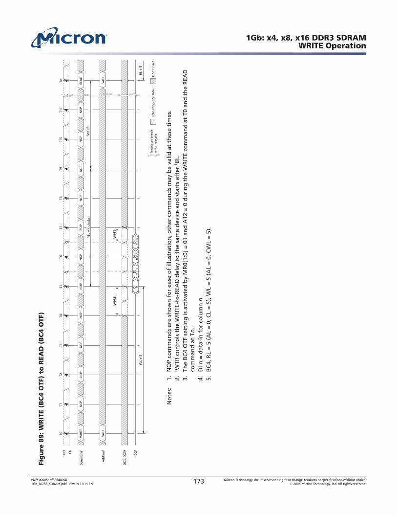
Fig
ure
89
: W
RIT
E (
BC
4 O
TF)
to R
EA
D (
BC
4 O
TF)
WL
= 5
RL
= 5
T0T1
T2T3
T4T5
T6T7
T8T9
t WPR
E
T10
T11
Do
n’t
Car
eTr
ansi
tio
nin
g D
ata
Tn
NO
PW
RITE
REA
D
Valid
Valid
NO
PN
OP
NO
PN
OP
NO
PN
OP
NO
PN
OP
NO
P
CKCK#
Com
man
d1
DQ
4
DQ
S, D
QS#
Add
ress
3
t WPS
T
t BL
= 4
clo
cks
NO
P
t WTR
2
Ind
icat
es b
reak
in t
ime
scal
e
DI
n +
3D
In
+ 2
DI
n +
1D
I n
No
tes:
1.N
OP
com
man
ds
are
sho
wn
fo
r ea
se o
f ill
ust
rati
on
; oth
er c
om
man
ds
may
be
valid
at
thes
e ti
mes
.2.
t WTR
co
ntr
ols
th
e W
RIT
E-to
-REA
D d
elay
to
th
e sa
me
dev
ice
and
sta
rts
afte
r t B
L.3.
The
BC
4 O
TF s
etti
ng
is a
ctiv
ated
by
MR
0[1:
0] =
01
and
A12
= 0
du
rin
g t
he
WR
ITE
com
man
d a
t T0
an
d t
he
REA
Dco
mm
and
at
Tn.
4.D
I n =
dat
a-in
fo
r co
lum
n n
.5.
BC
4, R
L =
5 (
AL
= 0
, CL
= 5
), W
L =
5 (
AL
= 0
, CW
L =
5).
1Gb: x4, x8, x16 DDR3 SDRAMWRITE Operation
PDF: 09005aef826aa9061Gb_DDR3_SDRAM.pdf - Rev. N 11/14 EN 173 Micron Technology, Inc. reserves the right to change products or specifications without notice.
© 2006 Micron Technology, Inc. All rights reserved.
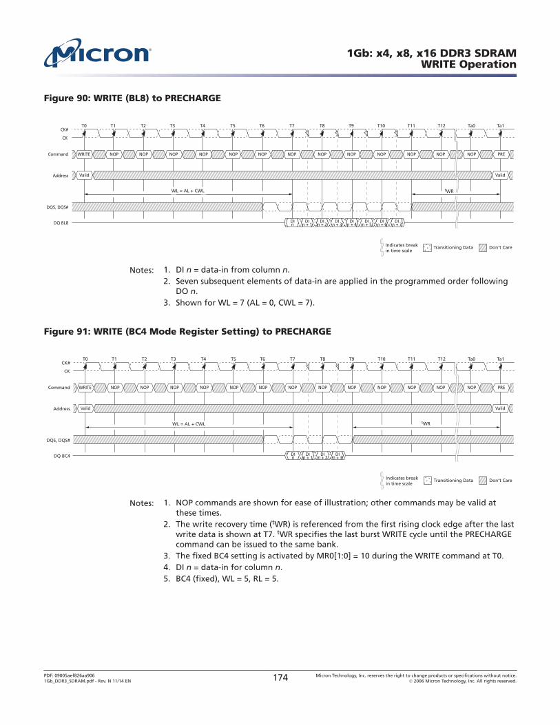
Figure 90: WRITE (BL8) to PRECHARGE
T0 T1 T2 T3 T4 T5 T6 T7 T8 T9 T10 T11 T12 Ta0 Ta1
DIn + 3
DIn + 2
DIn + 1
DIn
DIn + 6
DIn + 7
DIn + 5
DIn + 4
NOPWRITE
Valid
NOP NOP NOP NOP NOP NOP NOP NOP NOP NOP NOP NOP PRE
CK
CK#
Command
DQ BL8
DQS, DQS#
Address
Don’t CareTransitioning DataIndicates breakin time scale
tWRWL = AL + CWL
Valid
Notes: 1. DI n = data-in from column n.2. Seven subsequent elements of data-in are applied in the programmed order following
DO n.3. Shown for WL = 7 (AL = 0, CWL = 7).
Figure 91: WRITE (BC4 Mode Register Setting) to PRECHARGE
T0 T1 T2 T3 T4 T5 T6 T7 T8 T9 T10 T11 T12 Ta0 Ta1
DIn + 3
DIn + 2
DIn + 1
DIn
NOPWRITE
Valid
NOP NOP NOP NOP NOP NOP NOP NOP NOP NOP NOP NOP PRE
CK
CK#
Command
DQ BC4
DQS, DQS#
Address
Don’t CareTransitioning DataIndicates breakin time scale
tWRWL = AL + CWL
Valid
Notes: 1. NOP commands are shown for ease of illustration; other commands may be valid atthese times.
2. The write recovery time (tWR) is referenced from the first rising clock edge after the lastwrite data is shown at T7. tWR specifies the last burst WRITE cycle until the PRECHARGEcommand can be issued to the same bank.
3. The fixed BC4 setting is activated by MR0[1:0] = 10 during the WRITE command at T0.4. DI n = data-in for column n.5. BC4 (fixed), WL = 5, RL = 5.
1Gb: x4, x8, x16 DDR3 SDRAMWRITE Operation
PDF: 09005aef826aa9061Gb_DDR3_SDRAM.pdf - Rev. N 11/14 EN 174 Micron Technology, Inc. reserves the right to change products or specifications without notice.
© 2006 Micron Technology, Inc. All rights reserved.
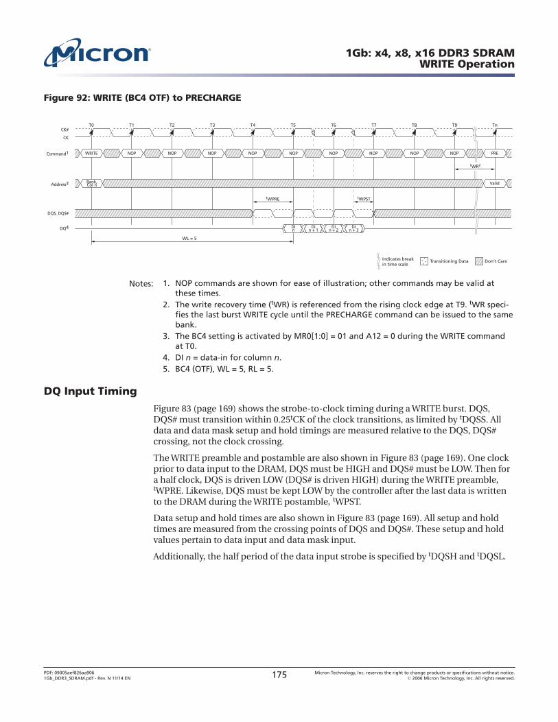
Figure 92: WRITE (BC4 OTF) to PRECHARGE
WL = 5
T0 T1 T2 T3 T4 T5 T6 T7 T8 T9 Tn
Don’t CareTransitioning Data
Bank,Col n
NOPWRITE PRENOP NOP NOP NOP NOP NOP NOPNOP
CK
CK#
Command1
DQ4
DQS, DQS#
Address3
tWPSTtWPRE
Indicates breakin time scale
DIn + 3
DIn + 2
DIn + 1
DIn
tWR2
Valid
Notes: 1. NOP commands are shown for ease of illustration; other commands may be valid atthese times.
2. The write recovery time (tWR) is referenced from the rising clock edge at T9. tWR speci-fies the last burst WRITE cycle until the PRECHARGE command can be issued to the samebank.
3. The BC4 setting is activated by MR0[1:0] = 01 and A12 = 0 during the WRITE commandat T0.
4. DI n = data-in for column n.5. BC4 (OTF), WL = 5, RL = 5.
DQ Input Timing
Figure 83 (page 169) shows the strobe-to-clock timing during a WRITE burst. DQS,DQS# must transition within 0.25tCK of the clock transitions, as limited by tDQSS. Alldata and data mask setup and hold timings are measured relative to the DQS, DQS#crossing, not the clock crossing.
The WRITE preamble and postamble are also shown in Figure 83 (page 169). One clockprior to data input to the DRAM, DQS must be HIGH and DQS# must be LOW. Then fora half clock, DQS is driven LOW (DQS# is driven HIGH) during the WRITE preamble,tWPRE. Likewise, DQS must be kept LOW by the controller after the last data is writtento the DRAM during the WRITE postamble, tWPST.
Data setup and hold times are also shown in Figure 83 (page 169). All setup and holdtimes are measured from the crossing points of DQS and DQS#. These setup and holdvalues pertain to data input and data mask input.
Additionally, the half period of the data input strobe is specified by tDQSH and tDQSL.
1Gb: x4, x8, x16 DDR3 SDRAMWRITE Operation
PDF: 09005aef826aa9061Gb_DDR3_SDRAM.pdf - Rev. N 11/14 EN 175 Micron Technology, Inc. reserves the right to change products or specifications without notice.
© 2006 Micron Technology, Inc. All rights reserved.
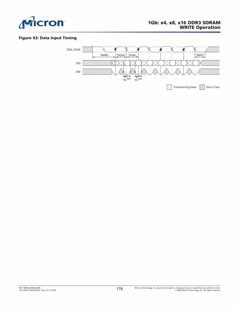
Figure 93: Data Input Timing
tDH tDHtDS tDS
DM
DQ DIb
DQS, DQS#
Don’t CareTransitioning Data
tDQSH tDQSLtWPRE tWPST
1Gb: x4, x8, x16 DDR3 SDRAMWRITE Operation
PDF: 09005aef826aa9061Gb_DDR3_SDRAM.pdf - Rev. N 11/14 EN 176 Micron Technology, Inc. reserves the right to change products or specifications without notice.
© 2006 Micron Technology, Inc. All rights reserved.
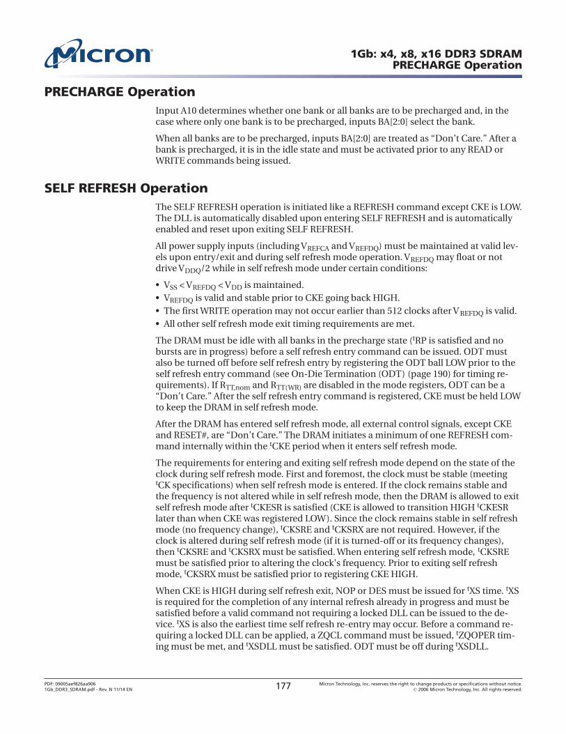
PRECHARGE OperationInput A10 determines whether one bank or all banks are to be precharged and, in thecase where only one bank is to be precharged, inputs BA[2:0] select the bank.
When all banks are to be precharged, inputs BA[2:0] are treated as “Don’t Care.” After abank is precharged, it is in the idle state and must be activated prior to any READ orWRITE commands being issued.
SELF REFRESH OperationThe SELF REFRESH operation is initiated like a REFRESH command except CKE is LOW.The DLL is automatically disabled upon entering SELF REFRESH and is automaticallyenabled and reset upon exiting SELF REFRESH.
All power supply inputs (including VREFCA and VREFDQ) must be maintained at valid lev-els upon entry/exit and during self refresh mode operation. VREFDQ may float or notdrive VDDQ/2 while in self refresh mode under certain conditions:
• VSS < VREFDQ < VDD is maintained.• VREFDQ is valid and stable prior to CKE going back HIGH.• The first WRITE operation may not occur earlier than 512 clocks after V REFDQ is valid.• All other self refresh mode exit timing requirements are met.
The DRAM must be idle with all banks in the precharge state (tRP is satisfied and nobursts are in progress) before a self refresh entry command can be issued. ODT mustalso be turned off before self refresh entry by registering the ODT ball LOW prior to theself refresh entry command (see On-Die Termination (ODT) (page 190) for timing re-quirements). If RTT,nom and RTT(WR) are disabled in the mode registers, ODT can be a“Don’t Care.” After the self refresh entry command is registered, CKE must be held LOWto keep the DRAM in self refresh mode.
After the DRAM has entered self refresh mode, all external control signals, except CKEand RESET#, are “Don’t Care.” The DRAM initiates a minimum of one REFRESH com-mand internally within the tCKE period when it enters self refresh mode.
The requirements for entering and exiting self refresh mode depend on the state of theclock during self refresh mode. First and foremost, the clock must be stable (meetingtCK specifications) when self refresh mode is entered. If the clock remains stable andthe frequency is not altered while in self refresh mode, then the DRAM is allowed to exitself refresh mode after tCKESR is satisfied (CKE is allowed to transition HIGH tCKESRlater than when CKE was registered LOW). Since the clock remains stable in self refreshmode (no frequency change), tCKSRE and tCKSRX are not required. However, if theclock is altered during self refresh mode (if it is turned-off or its frequency changes),then tCKSRE and tCKSRX must be satisfied. When entering self refresh mode, tCKSREmust be satisfied prior to altering the clock's frequency. Prior to exiting self refreshmode, tCKSRX must be satisfied prior to registering CKE HIGH.
When CKE is HIGH during self refresh exit, NOP or DES must be issued for tXS time. tXSis required for the completion of any internal refresh already in progress and must besatisfied before a valid command not requiring a locked DLL can be issued to the de-vice. tXS is also the earliest time self refresh re-entry may occur. Before a command re-quiring a locked DLL can be applied, a ZQCL command must be issued, tZQOPER tim-ing must be met, and tXSDLL must be satisfied. ODT must be off during tXSDLL.
1Gb: x4, x8, x16 DDR3 SDRAMPRECHARGE Operation
PDF: 09005aef826aa9061Gb_DDR3_SDRAM.pdf - Rev. N 11/14 EN 177 Micron Technology, Inc. reserves the right to change products or specifications without notice.
© 2006 Micron Technology, Inc. All rights reserved.
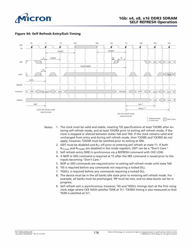
Figure 94: Self Refresh Entry/Exit Timing
CK
CK#
Command NOP NOP4SRE (REF)3
Address
CKE
ODT2
RESET#2
Valid
Valid6SRX (NOP) NOP5
tRP8
tXSDLL7, 9
ODTL
tIStCPDEDtIS
tIS
Enter self refresh mode(synchronous)
Exit self refresh mode(asynchronous)
T0 T1 T2 Tc0 Tc1 Td0Tb0
Don’t Care
Te0
Valid
Valid7
Valid
Valid Valid
tIH
Ta0 Tf0
Indicates breakin time scale
tCKSRX1tCKSRE1
tXS6, 9
tCKESR (MIN)1
Notes: 1. The clock must be valid and stable, meeting tCK specifications at least tCKSRE after en-tering self refresh mode, and at least tCKSRX prior to exiting self refresh mode, if theclock is stopped or altered between states Ta0 and Tb0. If the clock remains valid andunchanged from entry and during self refresh mode, then tCKSRE and tCKSRX do notapply; however, tCKESR must be satisfied prior to exiting at SRX.
2. ODT must be disabled and RTT off prior to entering self refresh at state T1. If bothRTT,nom and RTT(WR) are disabled in the mode registers, ODT can be a “Don’t Care.”
3. Self refresh entry (SRE) is synchronous via a REFRESH command with CKE LOW.4. A NOP or DES command is required at T2 after the SRE command is issued prior to the
inputs becoming “Don’t Care.”5. NOP or DES commands are required prior to exiting self refresh mode until state Te0.6. tXS is required before any commands not requiring a locked DLL.7. tXSDLL is required before any commands requiring a locked DLL.8. The device must be in the all banks idle state prior to entering self refresh mode. For
example, all banks must be precharged, tRP must be met, and no data bursts can be inprogress.
9. Self refresh exit is asynchronous; however, tXS and tXSDLL timings start at the first risingclock edge where CKE HIGH satisfies tISXR at Tc1. tCKSRX timing is also measured so thattISXR is satisfied at Tc1.
1Gb: x4, x8, x16 DDR3 SDRAMSELF REFRESH Operation
PDF: 09005aef826aa9061Gb_DDR3_SDRAM.pdf - Rev. N 11/14 EN 178 Micron Technology, Inc. reserves the right to change products or specifications without notice.
© 2006 Micron Technology, Inc. All rights reserved.
Extended Temperature UsageMicron’s DDR3 SDRAM support the optional extended case temperature (TC) range of0°C to 95°C. Thus, the SRT and ASR options must be used at a minimum.
The extended temperature range DRAM must be refreshed externally at 2x (double re-fresh) anytime the case temperature is above 85°C (and does not exceed 95°C). The ex-ternal refresh requirement is accomplished by reducing the refresh period from 64ms to32ms. However, self refresh mode requires either ASR or SRT to support the extendedtemperature. Thus, either ASR or SRT must be enabled when TC is above 85°C or selfrefresh cannot be used until TC is at or below 85°C. Table 78 summarizes the two exten-ded temperature options and Table 79 summarizes how the two extended temperatureoptions relate to one another.
Table 78: Self Refresh Temperature and Auto Self Refresh Description
Field MR2 Bits Description
Self Refresh Temperature (SRT)
SRT 7 If ASR is disabled (MR2[6] = 0), SRT must be programmed to indicate TOPER during self refresh:*MR2[7] = 0: Normal operating temperature range (0°C to 85°C)*MR2[7] = 1: Extended operating temperature range (0°C to 95°C)If ASR is enabled (MR2[7] = 1), SRT must be set to 0, even if the extended temperature range issupported*MR2[7] = 0: SRT is disabled
Auto Self Refresh (ASR)
ASR 6 When ASR is enabled, the DRAM automatically provides SELF REFRESH power management func-tions, (refresh rate for all supported operating temperature values)* MR2[6] = 1: ASR is enabled (M7 must = 0)When ASR is not enabled, the SRT bit must be programmed to indicate TOPER during SELF REFRESHoperation* MR2[6] = 0: ASR is disabled; must use manual self refresh temperature (SRT)
Table 79: Self Refresh Mode Summary
MR2[6](ASR)
MR2[7](SRT) SELF REFRESH Operation
Permitted Operating TemperatureRange for Self Refresh Mode
0 0 Self refresh mode is supported in the normal temperaturerange
Normal (0°C to 85°C)
0 1 Self refresh mode is supported in normal and extended temper-ature ranges; When SRT is enabled, it increases self refreshpower consumption
Normal and extended (0°C to 95°C)
1 0 Self refresh mode is supported in normal and extended temper-ature ranges; Self refresh power consumption may be tempera-ture-dependent
Normal and extended (0°C to 95°C)
1 1 Illegal
1Gb: x4, x8, x16 DDR3 SDRAMExtended Temperature Usage
PDF: 09005aef826aa9061Gb_DDR3_SDRAM.pdf - Rev. N 11/14 EN 179 Micron Technology, Inc. reserves the right to change products or specifications without notice.
© 2006 Micron Technology, Inc. All rights reserved.
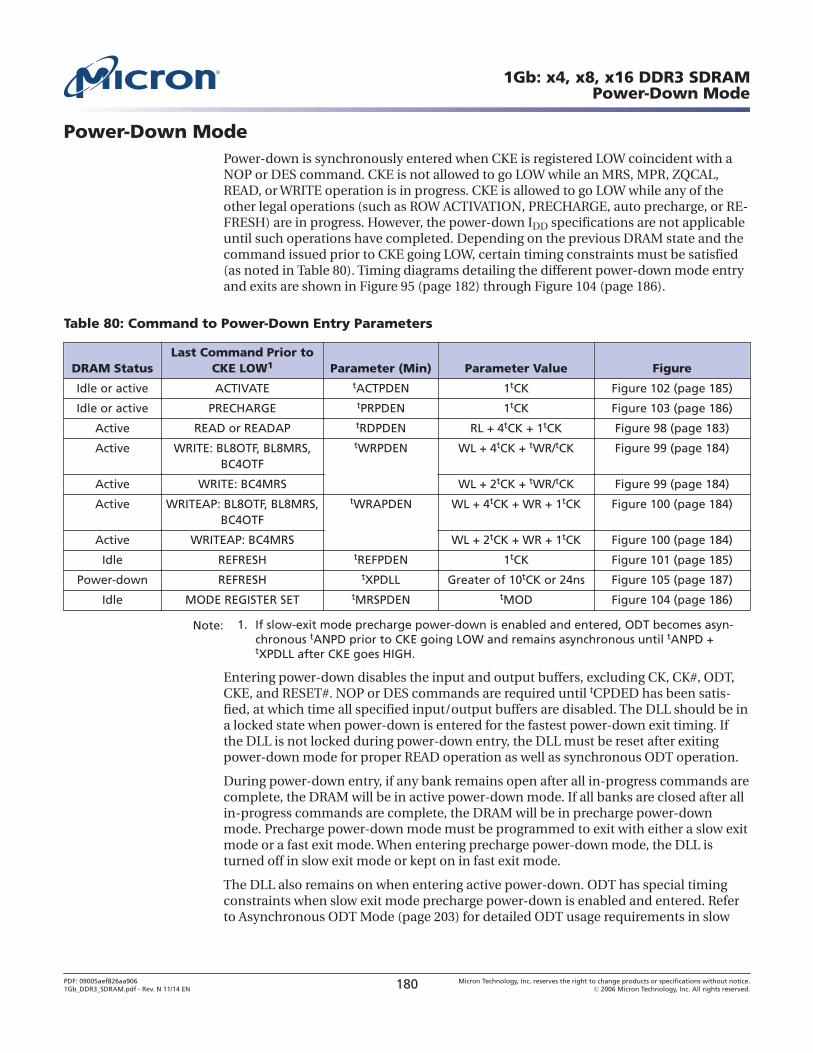
Power-Down ModePower-down is synchronously entered when CKE is registered LOW coincident with aNOP or DES command. CKE is not allowed to go LOW while an MRS, MPR, ZQCAL,READ, or WRITE operation is in progress. CKE is allowed to go LOW while any of theother legal operations (such as ROW ACTIVATION, PRECHARGE, auto precharge, or RE-FRESH) are in progress. However, the power-down IDD specifications are not applicableuntil such operations have completed. Depending on the previous DRAM state and thecommand issued prior to CKE going LOW, certain timing constraints must be satisfied(as noted in Table 80). Timing diagrams detailing the different power-down mode entryand exits are shown in Figure 95 (page 182) through Figure 104 (page 186).
Table 80: Command to Power-Down Entry Parameters
DRAM StatusLast Command Prior to
CKE LOW1 Parameter (Min) Parameter Value Figure
Idle or active ACTIVATE tACTPDEN 1tCK Figure 102 (page 185)
Idle or active PRECHARGE tPRPDEN 1tCK Figure 103 (page 186)
Active READ or READAP tRDPDEN RL + 4tCK + 1tCK Figure 98 (page 183)
Active WRITE: BL8OTF, BL8MRS,BC4OTF
tWRPDEN WL + 4tCK + tWR/tCK Figure 99 (page 184)
Active WRITE: BC4MRS WL + 2tCK + tWR/tCK Figure 99 (page 184)
Active WRITEAP: BL8OTF, BL8MRS,BC4OTF
tWRAPDEN WL + 4tCK + WR + 1tCK Figure 100 (page 184)
Active WRITEAP: BC4MRS WL + 2tCK + WR + 1tCK Figure 100 (page 184)
Idle REFRESH tREFPDEN 1tCK Figure 101 (page 185)
Power-down REFRESH tXPDLL Greater of 10tCK or 24ns Figure 105 (page 187)
Idle MODE REGISTER SET tMRSPDEN tMOD Figure 104 (page 186)
Note: 1. If slow-exit mode precharge power-down is enabled and entered, ODT becomes asyn-chronous tANPD prior to CKE going LOW and remains asynchronous until tANPD +tXPDLL after CKE goes HIGH.
Entering power-down disables the input and output buffers, excluding CK, CK#, ODT,CKE, and RESET#. NOP or DES commands are required until tCPDED has been satis-fied, at which time all specified input/output buffers are disabled. The DLL should be ina locked state when power-down is entered for the fastest power-down exit timing. Ifthe DLL is not locked during power-down entry, the DLL must be reset after exitingpower-down mode for proper READ operation as well as synchronous ODT operation.
During power-down entry, if any bank remains open after all in-progress commands arecomplete, the DRAM will be in active power-down mode. If all banks are closed after allin-progress commands are complete, the DRAM will be in precharge power-downmode. Precharge power-down mode must be programmed to exit with either a slow exitmode or a fast exit mode. When entering precharge power-down mode, the DLL isturned off in slow exit mode or kept on in fast exit mode.
The DLL also remains on when entering active power-down. ODT has special timingconstraints when slow exit mode precharge power-down is enabled and entered. Referto Asynchronous ODT Mode (page 203) for detailed ODT usage requirements in slow
1Gb: x4, x8, x16 DDR3 SDRAMPower-Down Mode
PDF: 09005aef826aa9061Gb_DDR3_SDRAM.pdf - Rev. N 11/14 EN 180 Micron Technology, Inc. reserves the right to change products or specifications without notice.
© 2006 Micron Technology, Inc. All rights reserved.
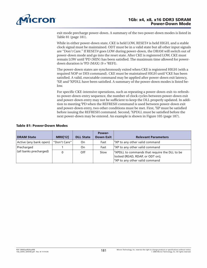
exit mode precharge power-down. A summary of the two power-down modes is listed inTable 81 (page 181).
While in either power-down state, CKE is held LOW, RESET# is held HIGH, and a stableclock signal must be maintained. ODT must be in a valid state but all other input signalsare “Don’t Care.” If RESET# goes LOW during power-down, the DRAM will switch out ofpower-down mode and go into the reset state. After CKE is registered LOW, CKE mustremain LOW until tPD (MIN) has been satisfied. The maximum time allowed for power-down duration is tPD (MAX) (9 × tREFI).
The power-down states are synchronously exited when CKE is registered HIGH (with arequired NOP or DES command). CKE must be maintained HIGH until tCKE has beensatisfied. A valid, executable command may be applied after power-down exit latency,tXP, and tXPDLL have been satisfied. A summary of the power-down modes is listed be-low.
For specific CKE-intensive operations, such as repeating a power-down-exit-to-refresh-to-power-down-entry sequence, the number of clock cycles between power-down exitand power-down entry may not be sufficient to keep the DLL properly updated. In addi-tion to meeting tPD when the REFRESH command is used between power-down exitand power-down entry, two other conditions must be met. First, tXP must be satisfiedbefore issuing the REFRESH command. Second, tXPDLL must be satisfied before thenext power-down may be entered. An example is shown in Figure 105 (page 187).
Table 81: Power-Down Modes
DRAM State MR0[12] DLL StatePower-
Down Exit Relevant Parameters
Active (any bank open) “Don’t Care” On Fast tXP to any other valid command
Precharged(all banks precharged)
1 On Fast tXP to any other valid command
0 Off Slow tXPDLL to commands that require the DLL to belocked (READ, RDAP, or ODT on);tXP to any other valid command
1Gb: x4, x8, x16 DDR3 SDRAMPower-Down Mode
PDF: 09005aef826aa9061Gb_DDR3_SDRAM.pdf - Rev. N 11/14 EN 181 Micron Technology, Inc. reserves the right to change products or specifications without notice.
© 2006 Micron Technology, Inc. All rights reserved.
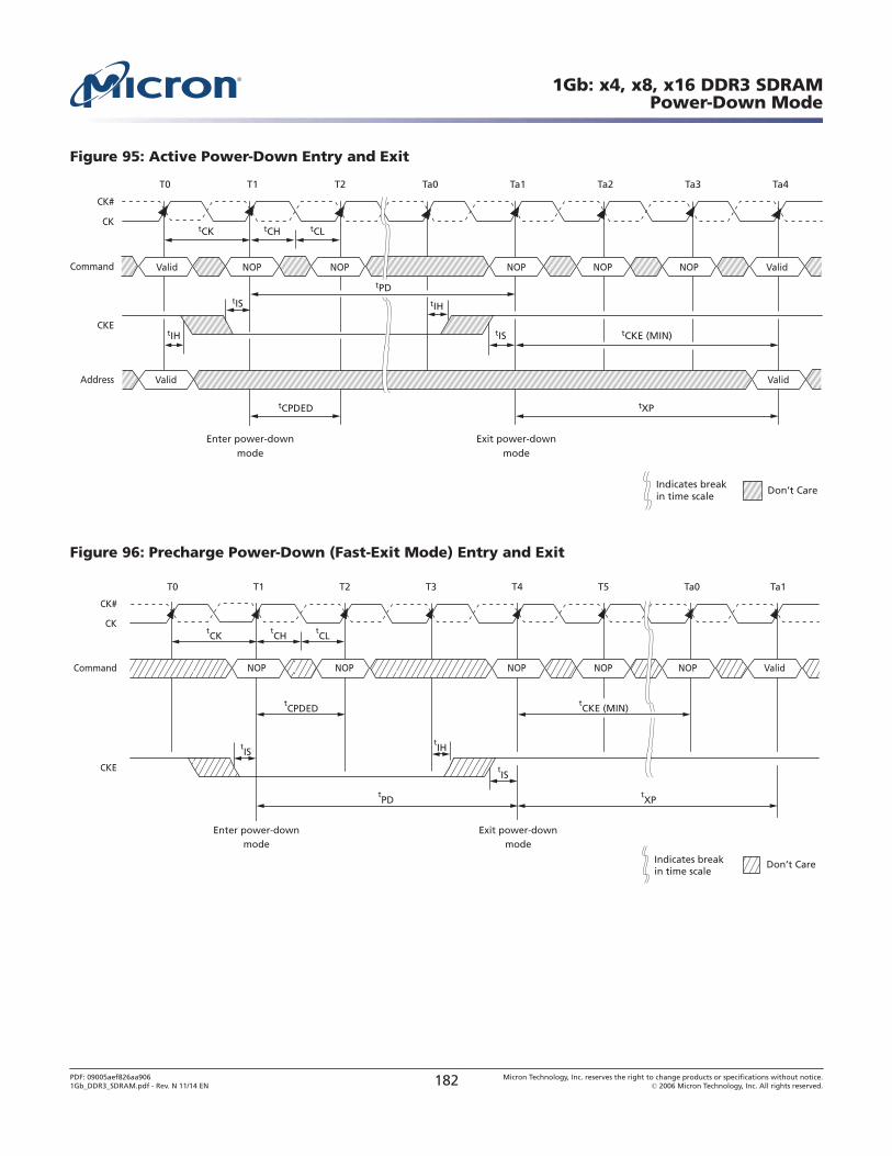
Figure 95: Active Power-Down Entry and Exit
CK
CK#
Command NOP NOP NOP NOP
Address
CKE
tCK tCH tCL
Enter power-downmode
Exit power-downmode
Don’t Care
ValidValid
Valid
tCPDED
Valid
tIS
tIH
tIH
tIS
T0 T1 T2 Ta0 Ta1 Ta2 Ta3 Ta4
NOP
tXP
tCKE (MIN)
Indicates breakin time scale
tPD
Figure 96: Precharge Power-Down (Fast-Exit Mode) Entry and Exit
CK
CK#
Command NOP NOP NOP NOP
CKE
tCK
tCH
tCL
Enter power-downmode
Exit power-downmode
tPD
Valid
tCPDED
tIS
tIHt
IS
T0 T1 T2 T3 T4 T5 Ta0 Ta1
NOP
Don’t CareIndicates breakin time scale
tXP
tCKE (MIN)
1Gb: x4, x8, x16 DDR3 SDRAMPower-Down Mode
PDF: 09005aef826aa9061Gb_DDR3_SDRAM.pdf - Rev. N 11/14 EN 182 Micron Technology, Inc. reserves the right to change products or specifications without notice.
© 2006 Micron Technology, Inc. All rights reserved.
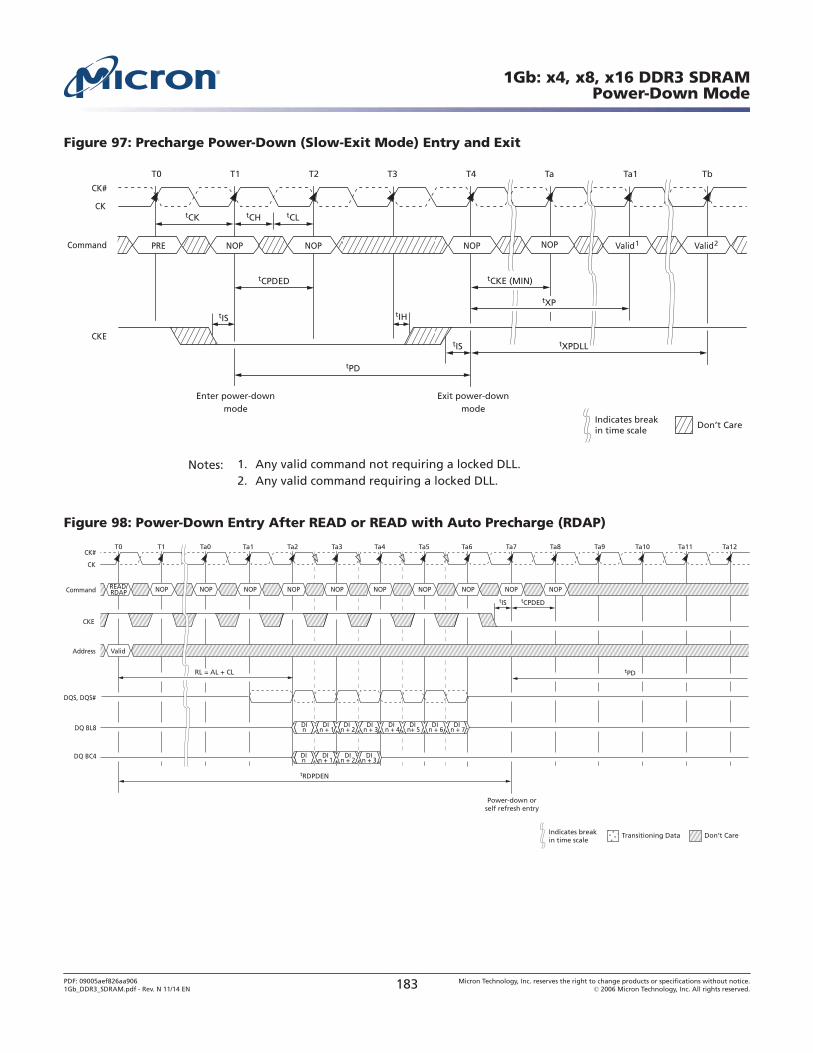
Figure 97: Precharge Power-Down (Slow-Exit Mode) Entry and Exit
CK
CK#
Command NOP NOP NOP
CKE
tCK tCH tCL
Enter power-downmode
Exit power-downmode
tPD
Valid2Valid1PRE
tXPDLL
tCPDED
tIS
tIHtIS
T0 T1 T2 T3 T4 Ta Ta1 Tb
NOP
Don’t CareIndicates breakin time scale
tXP
tCKE (MIN)
Notes: 1. Any valid command not requiring a locked DLL.2. Any valid command requiring a locked DLL.
Figure 98: Power-Down Entry After READ or READ with Auto Precharge (RDAP)
T0 T1 Ta0 Ta1 Ta2 Ta3 Ta4 Ta5 Ta6 Ta7 Ta8 Ta9
Don’t CareTransitioning Data
Ta10 Ta11 Ta12
NOP
Valid
READ/RDAP NOP NOP NOP NOP NOP NOP NOP NOP NOP
CK
CK#
Command
DQ BL8
DQ BC4
DQS, DQS#
Address
CKE
tCPDEDtIS
tPD
Power-down orself refresh entry
Indicates breakin time scale
tRDPDEN
DIn + 3
DIn + 1
DIn + 2
DIn
RL = AL + CL
DIn + 3
DIn + 2
DIn + 1
DIn
DIn + 6
DIn + 7
DIn+ 5
DIn + 4
1Gb: x4, x8, x16 DDR3 SDRAMPower-Down Mode
PDF: 09005aef826aa9061Gb_DDR3_SDRAM.pdf - Rev. N 11/14 EN 183 Micron Technology, Inc. reserves the right to change products or specifications without notice.
© 2006 Micron Technology, Inc. All rights reserved.
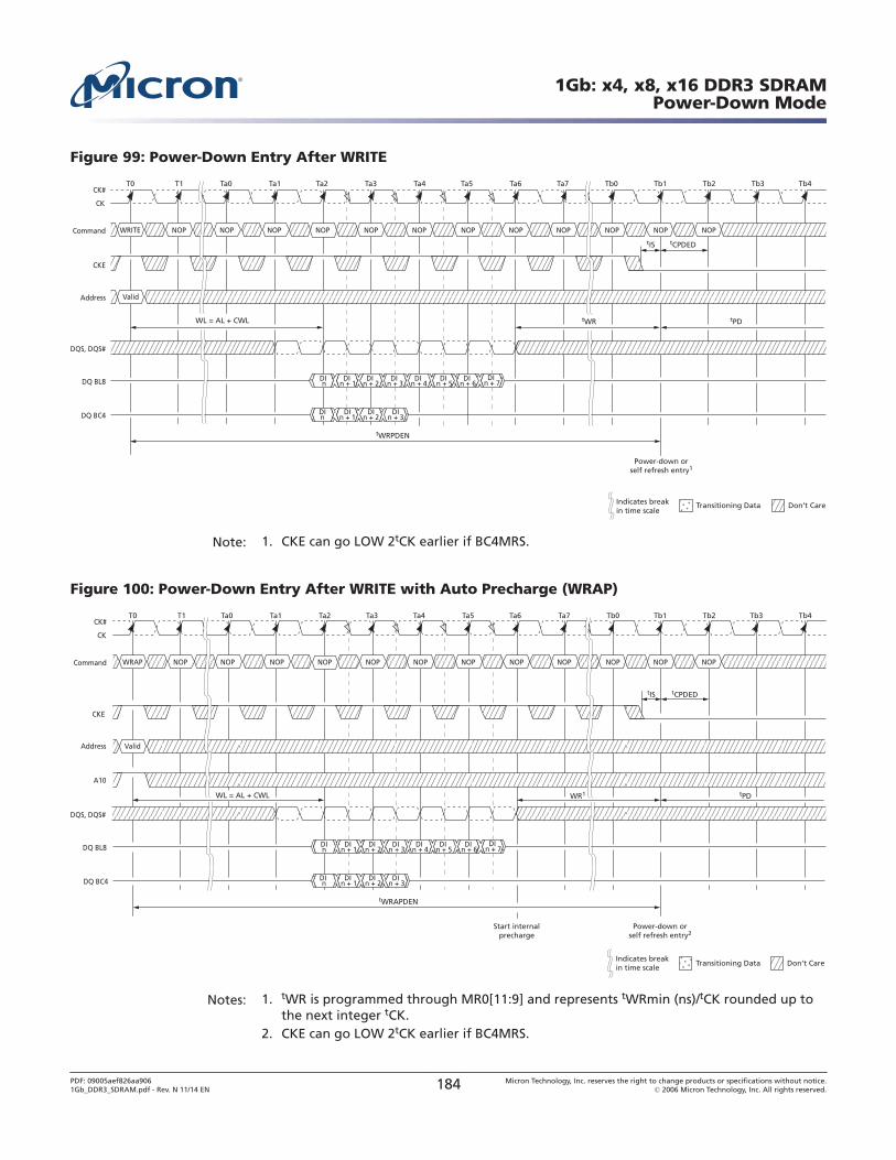
Figure 99: Power-Down Entry After WRITE
T0 T1 Ta0 Ta1 Ta2 Ta3 Ta4 Ta5 Ta6 Ta7 Tb0 Tb1 Tb2 Tb3 Tb4
NOPWRITE
Valid
NOP NOP NOP NOP NOP NOP NOP NOP NOP NOP NOP
CK
CK#
Command
DQ BL8
DQ BC4
DQS, DQS#
Address
CKE
tCPDED
Power-down orself refresh entry1
Don’t CareTransitioning Data
tWRPDEN
DIn + 3
DIn + 1
DIn + 2
DIn
tPD
Indicates breakin time scale
DI n + 3
DI n + 2
DI n + 1
DI n
DI n + 6
DI n + 7
DI n + 5
DI n + 4
tIS
WL = AL + CWL tWR
Note: 1. CKE can go LOW 2tCK earlier if BC4MRS.
Figure 100: Power-Down Entry After WRITE with Auto Precharge (WRAP)
T0 T1 Ta0 Ta1 Ta2 Ta3 Ta4 Ta5 Ta6 Ta7 Tb0 Tb1
Don’t CareTransitioning Data
Tb2 Tb3 Tb4
NOPWRAP
Valid
NOP NOP NOP NOP NOP NOP NOP NOP NOP NOP NOP
CK
CK#
Command
DQ BL8
DQ BC4
DQS, DQS#
Address
A10
CKE
tPD
tWRAPDEN
Power-down orself refresh entry2
Start internalprecharge
tCPDEDtIS
Indicates breakin time scale
DI n + 3
DI n + 2
DI n + 1
DIn
DI n + 6
DI n + 7
DI n + 5
DI n + 4
DI n + 3
DI n + 2
DI n + 1
DI n
WR1WL = AL + CWL
Notes: 1. tWR is programmed through MR0[11:9] and represents tWRmin (ns)/tCK rounded up tothe next integer tCK.
2. CKE can go LOW 2tCK earlier if BC4MRS.
1Gb: x4, x8, x16 DDR3 SDRAMPower-Down Mode
PDF: 09005aef826aa9061Gb_DDR3_SDRAM.pdf - Rev. N 11/14 EN 184 Micron Technology, Inc. reserves the right to change products or specifications without notice.
© 2006 Micron Technology, Inc. All rights reserved.
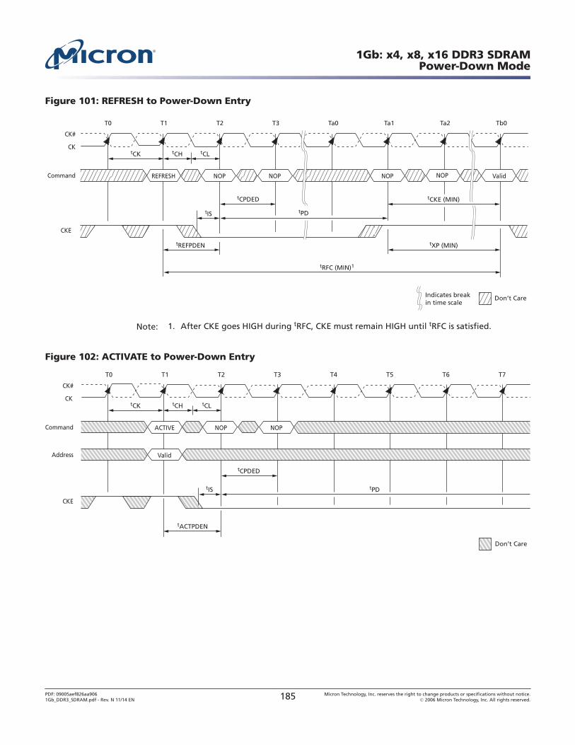
Figure 101: REFRESH to Power-Down Entry
CK
CK#
Command REFRESH NOP NOP NOP NOP Valid
CKE
tCK tCH tCL
tCPDED
tREFPDEN
tIS
T0 T1 T2 T3 Ta0 Ta1 Ta2 Tb0
tXP (MIN)
tRFC (MIN)1
Don’t CareIndicates breakin time scale
tCKE (MIN)
tPD
Note: 1. After CKE goes HIGH during tRFC, CKE must remain HIGH until tRFC is satisfied.
Figure 102: ACTIVATE to Power-Down Entry
CK
CK#
Command
Address
ACTIVE NOP NOP
CKE
tCK tCH tCL
Don’t Care
tCPDED
tACTPDEN
Valid
tIS
T0 T1 T2 T3 T4 T5 T6 T7
tPD
1Gb: x4, x8, x16 DDR3 SDRAMPower-Down Mode
PDF: 09005aef826aa9061Gb_DDR3_SDRAM.pdf - Rev. N 11/14 EN 185 Micron Technology, Inc. reserves the right to change products or specifications without notice.
© 2006 Micron Technology, Inc. All rights reserved.
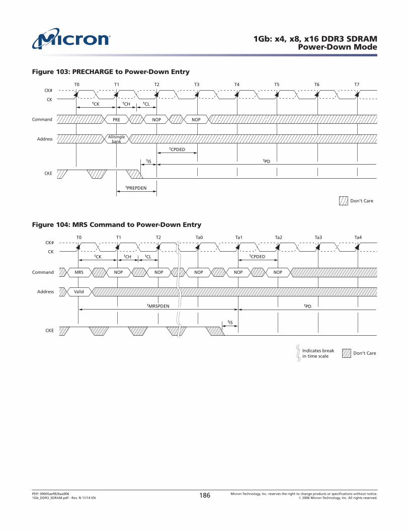
Figure 103: PRECHARGE to Power-Down Entry
CK
CK#
Command
Address
CKE
tCK tCH tCL
Don’t Care
tCPDED
tPREPDEN
tIS
T0 T1 T2 T3 T4 T5 T6 T7
tPD
All/singlebank
PRE NOP NOP
Figure 104: MRS Command to Power-Down Entry
CK
CK#
CKE
tCK tCH tCL tCPDED
Address
tIS
T0 T1 T2 Ta0 Ta1 Ta2 Ta3 Ta4
tPD
Don’t CareIndicates breakin time scale
Valid
Command MRS NOPNOP NOP NOP NOP
tMRSPDEN
1Gb: x4, x8, x16 DDR3 SDRAMPower-Down Mode
PDF: 09005aef826aa9061Gb_DDR3_SDRAM.pdf - Rev. N 11/14 EN 186 Micron Technology, Inc. reserves the right to change products or specifications without notice.
© 2006 Micron Technology, Inc. All rights reserved.
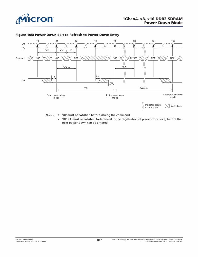
Figure 105: Power-Down Exit to Refresh to Power-Down Entry
CK
CK#
CKE
tCK tCH tCL
Enter power-downmode
Enter power-downmode
Exit power-downmode
tPD
tCPDED
tIS
tIHtIS
T0 T1 T2 T3 T4 Ta0 Ta1 Tb0
Don’t CareIndicates breakin time scale
Command NOP NOP NOP NOPREFRESH NOPNOP
tXP1
tXPDLL2
Notes: 1. tXP must be satisfied before issuing the command.2. tXPDLL must be satisfied (referenced to the registration of power-down exit) before the
next power-down can be entered.
1Gb: x4, x8, x16 DDR3 SDRAMPower-Down Mode
PDF: 09005aef826aa9061Gb_DDR3_SDRAM.pdf - Rev. N 11/14 EN 187 Micron Technology, Inc. reserves the right to change products or specifications without notice.
© 2006 Micron Technology, Inc. All rights reserved.
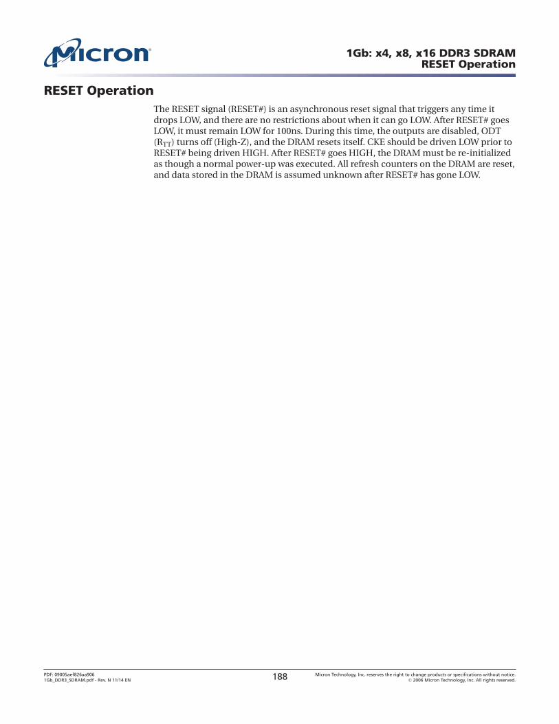
RESET OperationThe RESET signal (RESET#) is an asynchronous reset signal that triggers any time itdrops LOW, and there are no restrictions about when it can go LOW. After RESET# goesLOW, it must remain LOW for 100ns. During this time, the outputs are disabled, ODT(RTT) turns off (High-Z), and the DRAM resets itself. CKE should be driven LOW prior toRESET# being driven HIGH. After RESET# goes HIGH, the DRAM must be re-initializedas though a normal power-up was executed. All refresh counters on the DRAM are reset,and data stored in the DRAM is assumed unknown after RESET# has gone LOW.
1Gb: x4, x8, x16 DDR3 SDRAMRESET Operation
PDF: 09005aef826aa9061Gb_DDR3_SDRAM.pdf - Rev. N 11/14 EN 188 Micron Technology, Inc. reserves the right to change products or specifications without notice.
© 2006 Micron Technology, Inc. All rights reserved.
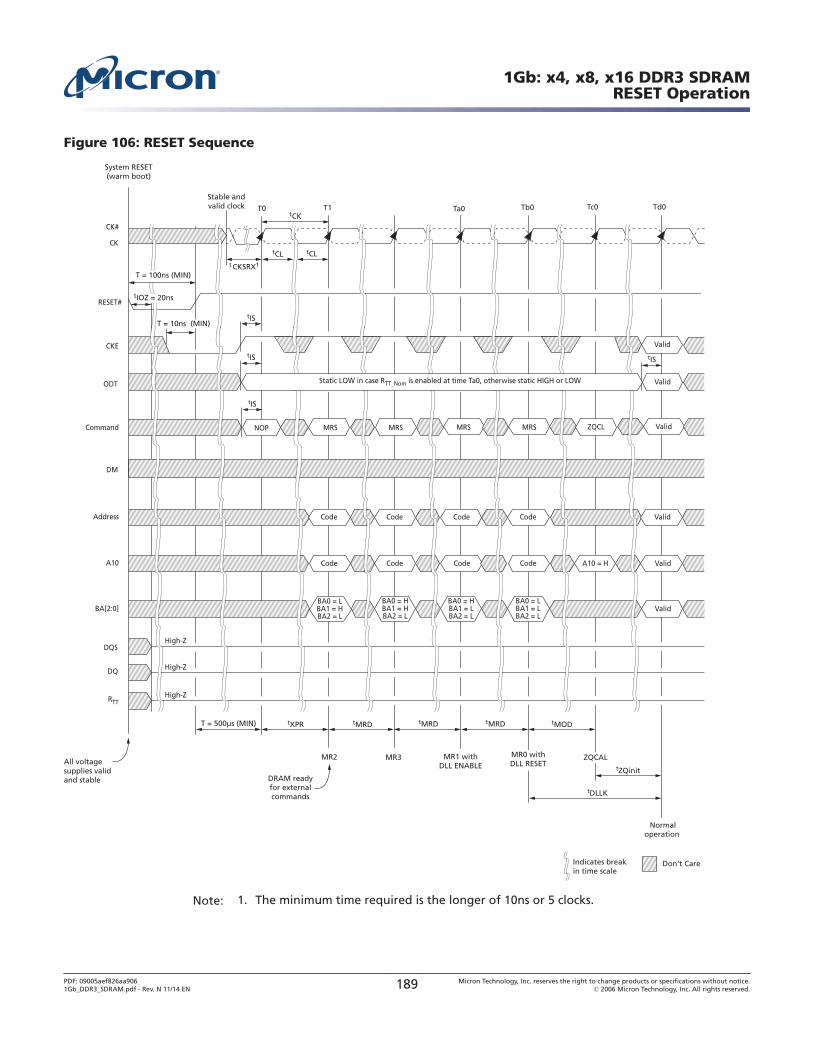
Figure 106: RESET Sequence
T = 10ns (MIN)
T = 100ns (MIN)
T = 500μs (MIN) tXPR tMRD tMRD tMRD tMOD
tCK
tIOZ = 20ns
CKE
RTT
BA[2:0]
All voltagesupplies validand stable
High-Z
DM
DQSHigh-Z
Address
A10
CK
CK#
tCL
Command NOP
T0 Ta0
Don’t Care
tCL
ODT
DQ High-Z
Tb0
tDLLK
MR1 withDLL ENABLE
MRSMRS
BA0 = HBA1 = LBA2 = L
BA0 = LBA1 = LBA2 = L
Code Code
Code Code
Valid
Valid
Valid
Valid
Normaloperation
MR2 MR3
MRSMRS
BA0 = LBA1 = HBA2 = L
BA0 = HBA1 = HBA2 = L
Code Code
Code Code
Tc0 Td0
RESET#
Stable andvalid clock
Valid
DRAM readyfor externalcommands
T1
tZQinit
A10 = H
ZQCL
tIS
Valid
System RESET(warm boot)
ZQCALMR0 withDLL RESET
Indicates breakin time scale
t CKSRX1
tIS
tIS
tIS
Static LOW in case RTT_Nom is enabled at time Ta0, otherwise static HIGH or LOW
Note: 1. The minimum time required is the longer of 10ns or 5 clocks.
1Gb: x4, x8, x16 DDR3 SDRAMRESET Operation
PDF: 09005aef826aa9061Gb_DDR3_SDRAM.pdf - Rev. N 11/14 EN 189 Micron Technology, Inc. reserves the right to change products or specifications without notice.
© 2006 Micron Technology, Inc. All rights reserved.
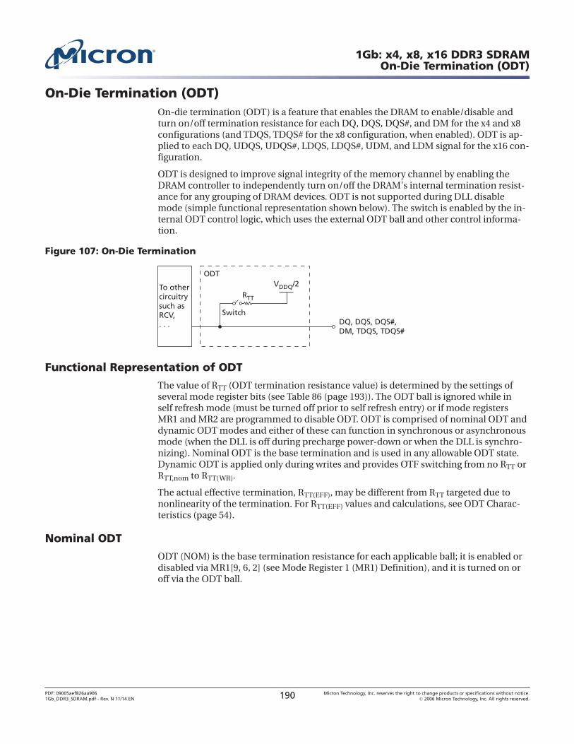
On-Die Termination (ODT)On-die termination (ODT) is a feature that enables the DRAM to enable/disable andturn on/off termination resistance for each DQ, DQS, DQS#, and DM for the x4 and x8configurations (and TDQS, TDQS# for the x8 configuration, when enabled). ODT is ap-plied to each DQ, UDQS, UDQS#, LDQS, LDQS#, UDM, and LDM signal for the x16 con-figuration.
ODT is designed to improve signal integrity of the memory channel by enabling theDRAM controller to independently turn on/off the DRAM’s internal termination resist-ance for any grouping of DRAM devices. ODT is not supported during DLL disablemode (simple functional representation shown below). The switch is enabled by the in-ternal ODT control logic, which uses the external ODT ball and other control informa-tion.
Figure 107: On-Die Termination
ODTVDDQ/2
RTT
SwitchDQ, DQS, DQS#, DM, TDQS, TDQS#
To othercircuitrysuch asRCV, . . .
Functional Representation of ODT
The value of RTT (ODT termination resistance value) is determined by the settings ofseveral mode register bits (see Table 86 (page 193)). The ODT ball is ignored while inself refresh mode (must be turned off prior to self refresh entry) or if mode registersMR1 and MR2 are programmed to disable ODT. ODT is comprised of nominal ODT anddynamic ODT modes and either of these can function in synchronous or asynchronousmode (when the DLL is off during precharge power-down or when the DLL is synchro-nizing). Nominal ODT is the base termination and is used in any allowable ODT state.Dynamic ODT is applied only during writes and provides OTF switching from no RTT orRTT,nom to RTT(WR).
The actual effective termination, RTT(EFF), may be different from RTT targeted due tononlinearity of the termination. For RTT(EFF) values and calculations, see ODT Charac-teristics (page 54).
Nominal ODT
ODT (NOM) is the base termination resistance for each applicable ball; it is enabled ordisabled via MR1[9, 6, 2] (see Mode Register 1 (MR1) Definition), and it is turned on oroff via the ODT ball.
1Gb: x4, x8, x16 DDR3 SDRAMOn-Die Termination (ODT)
PDF: 09005aef826aa9061Gb_DDR3_SDRAM.pdf - Rev. N 11/14 EN 190 Micron Technology, Inc. reserves the right to change products or specifications without notice.
© 2006 Micron Technology, Inc. All rights reserved.
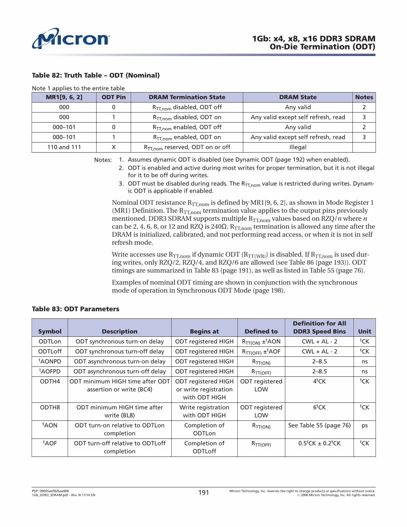
Table 82: Truth Table – ODT (Nominal)
Note 1 applies to the entire tableMR1[9, 6, 2] ODT Pin DRAM Termination State DRAM State Notes
000 0 RTT,nom disabled, ODT off Any valid 2
000 1 RTT,nom disabled, ODT on Any valid except self refresh, read 3
000–101 0 RTT,nom enabled, ODT off Any valid 2
000–101 1 RTT,nom enabled, ODT on Any valid except self refresh, read 3
110 and 111 X RTT,nom reserved, ODT on or off Illegal
Notes: 1. Assumes dynamic ODT is disabled (see Dynamic ODT (page 192) when enabled).2. ODT is enabled and active during most writes for proper termination, but it is not illegal
for it to be off during writes.3. ODT must be disabled during reads. The RTT,nom value is restricted during writes. Dynam-
ic ODT is applicable if enabled.
Nominal ODT resistance RTT,nom is defined by MR1[9, 6, 2], as shown in Mode Register 1(MR1) Definition. The RTT,nom termination value applies to the output pins previouslymentioned. DDR3 SDRAM supports multiple RTT,nom values based on RZQ/n where ncan be 2, 4, 6, 8, or 12 and RZQ is 240Ω. RTT,nom termination is allowed any time after theDRAM is initialized, calibrated, and not performing read access, or when it is not in selfrefresh mode.
Write accesses use RTT,nom if dynamic ODT (RTT(WR)) is disabled. If RTT,nom is used dur-ing writes, only RZQ/2, RZQ/4, and RZQ/6 are allowed (see Table 86 (page 193)). ODTtimings are summarized in Table 83 (page 191), as well as listed in Table 55 (page 76).
Examples of nominal ODT timing are shown in conjunction with the synchronousmode of operation in Synchronous ODT Mode (page 198).
Table 83: ODT Parameters
Symbol Description Begins at Defined toDefinition for AllDDR3 Speed Bins Unit
ODTLon ODT synchronous turn-on delay ODT registered HIGH RTT(ON) ±tAON CWL + AL - 2 tCK
ODTLoff ODT synchronous turn-off delay ODT registered HIGH RTT(OFF) ±tAOF CWL + AL - 2 tCKtAONPD ODT asynchronous turn-on delay ODT registered HIGH RTT(ON) 2–8.5 nstAOFPD ODT asynchronous turn-off delay ODT registered HIGH RTT(OFF) 2–8.5 ns
ODTH4 ODT minimum HIGH time after ODTassertion or write (BC4)
ODT registered HIGHor write registration
with ODT HIGH
ODT registeredLOW
4tCK tCK
ODTH8 ODT minimum HIGH time afterwrite (BL8)
Write registrationwith ODT HIGH
ODT registeredLOW
6tCK tCK
tAON ODT turn-on relative to ODTLoncompletion
Completion ofODTLon
RTT(ON) See Table 55 (page 76) ps
tAOF ODT turn-off relative to ODTLoffcompletion
Completion ofODTLoff
RTT(OFF) 0.5tCK ± 0.2tCK tCK
1Gb: x4, x8, x16 DDR3 SDRAMOn-Die Termination (ODT)
PDF: 09005aef826aa9061Gb_DDR3_SDRAM.pdf - Rev. N 11/14 EN 191 Micron Technology, Inc. reserves the right to change products or specifications without notice.
© 2006 Micron Technology, Inc. All rights reserved.
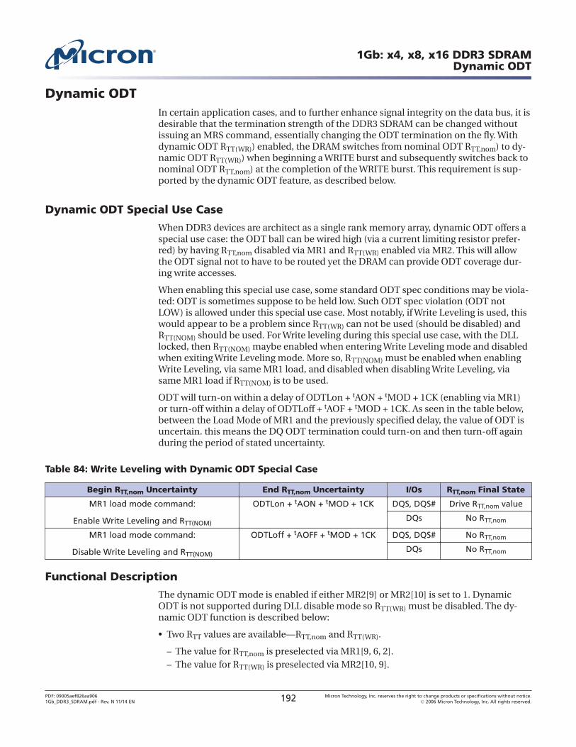
Dynamic ODTIn certain application cases, and to further enhance signal integrity on the data bus, it isdesirable that the termination strength of the DDR3 SDRAM can be changed withoutissuing an MRS command, essentially changing the ODT termination on the fly. Withdynamic ODT RTT(WR)) enabled, the DRAM switches from nominal ODT RTT,nom) to dy-namic ODT RTT(WR)) when beginning a WRITE burst and subsequently switches back tonominal ODT RTT,nom) at the completion of the WRITE burst. This requirement is sup-ported by the dynamic ODT feature, as described below.
Dynamic ODT Special Use Case
When DDR3 devices are architect as a single rank memory array, dynamic ODT offers aspecial use case: the ODT ball can be wired high (via a current limiting resistor prefer-red) by having RTT,nom disabled via MR1 and RTT(WR) enabled via MR2. This will allowthe ODT signal not to have to be routed yet the DRAM can provide ODT coverage dur-ing write accesses.
When enabling this special use case, some standard ODT spec conditions may be viola-ted: ODT is sometimes suppose to be held low. Such ODT spec violation (ODT notLOW) is allowed under this special use case. Most notably, if Write Leveling is used, thiswould appear to be a problem since RTT(WR) can not be used (should be disabled) andRTT(NOM) should be used. For Write leveling during this special use case, with the DLLlocked, then RTT(NOM) maybe enabled when entering Write Leveling mode and disabledwhen exiting Write Leveling mode. More so, RTT(NOM) must be enabled when enablingWrite Leveling, via same MR1 load, and disabled when disabling Write Leveling, viasame MR1 load if RTT(NOM) is to be used.
ODT will turn-on within a delay of ODTLon + tAON + tMOD + 1CK (enabling via MR1)or turn-off within a delay of ODTLoff + tAOF + tMOD + 1CK. As seen in the table below,between the Load Mode of MR1 and the previously specified delay, the value of ODT isuncertain. this means the DQ ODT termination could turn-on and then turn-off againduring the period of stated uncertainty.
Table 84: Write Leveling with Dynamic ODT Special Case
Begin RTT,nom Uncertainty End RTT,nom Uncertainty I/Os RTT,nom Final State
MR1 load mode command:
Enable Write Leveling and RTT(NOM)
ODTLon + tAON + tMOD + 1CK DQS, DQS# Drive RTT,nom value
DQs No RTT,nom
MR1 load mode command:
Disable Write Leveling and RTT(NOM)
ODTLoff + tAOFF + tMOD + 1CK DQS, DQS# No RTT,nom
DQs No RTT,nom
Functional Description
The dynamic ODT mode is enabled if either MR2[9] or MR2[10] is set to 1. DynamicODT is not supported during DLL disable mode so RTT(WR) must be disabled. The dy-namic ODT function is described below:
• Two RTT values are available—RTT,nom and RTT(WR).
– The value for RTT,nom is preselected via MR1[9, 6, 2].– The value for RTT(WR) is preselected via MR2[10, 9].
1Gb: x4, x8, x16 DDR3 SDRAMDynamic ODT
PDF: 09005aef826aa9061Gb_DDR3_SDRAM.pdf - Rev. N 11/14 EN 192 Micron Technology, Inc. reserves the right to change products or specifications without notice.
© 2006 Micron Technology, Inc. All rights reserved.
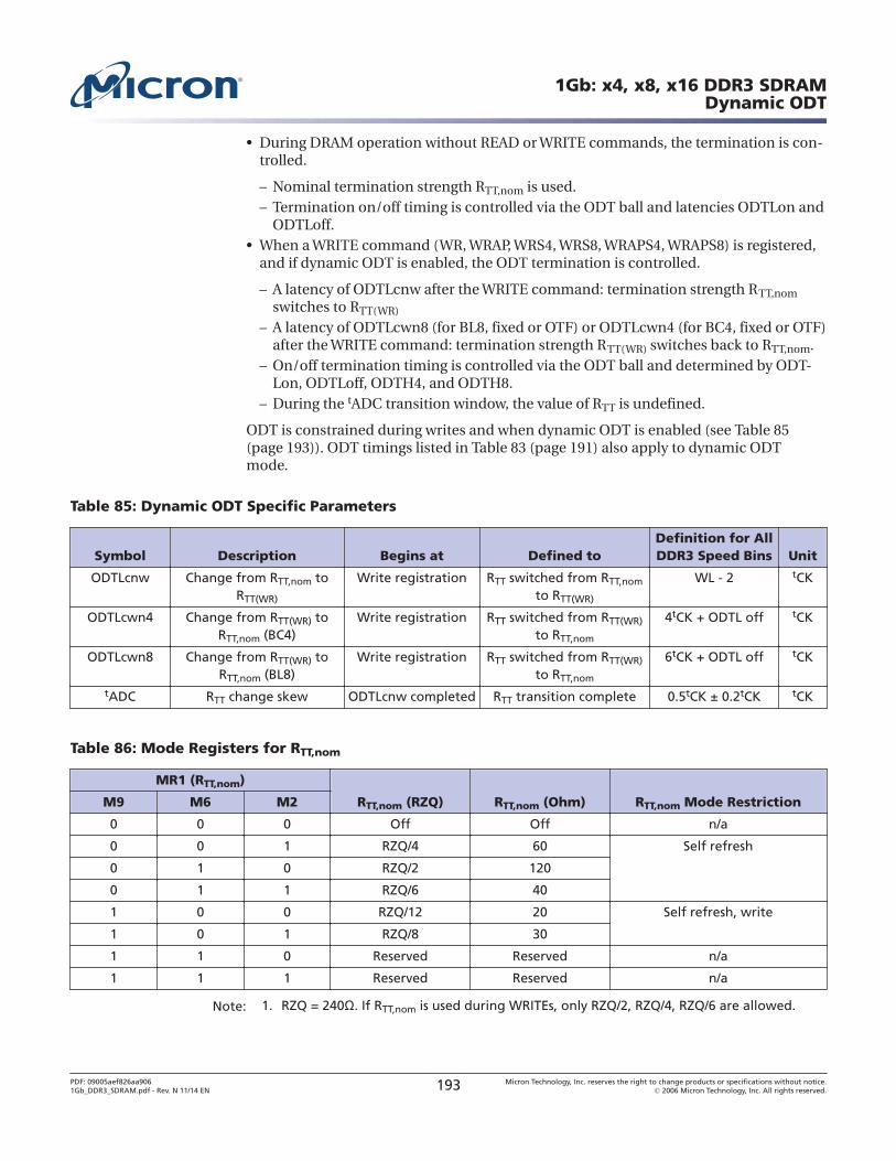
• During DRAM operation without READ or WRITE commands, the termination is con-trolled.
– Nominal termination strength RTT,nom is used.– Termination on/off timing is controlled via the ODT ball and latencies ODTLon and
ODTLoff.• When a WRITE command (WR, WRAP, WRS4, WRS8, WRAPS4, WRAPS8) is registered,
and if dynamic ODT is enabled, the ODT termination is controlled.
– A latency of ODTLcnw after the WRITE command: termination strength RTT,nomswitches to RTT(WR)
– A latency of ODTLcwn8 (for BL8, fixed or OTF) or ODTLcwn4 (for BC4, fixed or OTF)after the WRITE command: termination strength RTT(WR) switches back to RTT,nom.
– On/off termination timing is controlled via the ODT ball and determined by ODT-Lon, ODTLoff, ODTH4, and ODTH8.
– During the tADC transition window, the value of RTT is undefined.
ODT is constrained during writes and when dynamic ODT is enabled (see Table 85(page 193)). ODT timings listed in Table 83 (page 191) also apply to dynamic ODTmode.
Table 85: Dynamic ODT Specific Parameters
Symbol Description Begins at Defined toDefinition for AllDDR3 Speed Bins Unit
ODTLcnw Change from RTT,nom toRTT(WR)
Write registration RTT switched from RTT,nom
to RTT(WR)
WL - 2 tCK
ODTLcwn4 Change from RTT(WR) toRTT,nom (BC4)
Write registration RTT switched from RTT(WR)
to RTT,nom
4tCK + ODTL off tCK
ODTLcwn8 Change from RTT(WR) toRTT,nom (BL8)
Write registration RTT switched from RTT(WR)
to RTT,nom
6tCK + ODTL off tCK
tADC RTT change skew ODTLcnw completed RTT transition complete 0.5tCK ± 0.2tCK tCK
Table 86: Mode Registers for RTT,nom
MR1 (RTT,nom)
RTT,nom (RZQ) RTT,nom (Ohm) RTT,nom Mode RestrictionM9 M6 M2
0 0 0 Off Off n/a
0 0 1 RZQ/4 60 Self refresh
0 1 0 RZQ/2 120
0 1 1 RZQ/6 40
1 0 0 RZQ/12 20 Self refresh, write
1 0 1 RZQ/8 30
1 1 0 Reserved Reserved n/a
1 1 1 Reserved Reserved n/a
Note: 1. RZQ = 240Ω. If RTT,nom is used during WRITEs, only RZQ/2, RZQ/4, RZQ/6 are allowed.
1Gb: x4, x8, x16 DDR3 SDRAMDynamic ODT
PDF: 09005aef826aa9061Gb_DDR3_SDRAM.pdf - Rev. N 11/14 EN 193 Micron Technology, Inc. reserves the right to change products or specifications without notice.
© 2006 Micron Technology, Inc. All rights reserved.
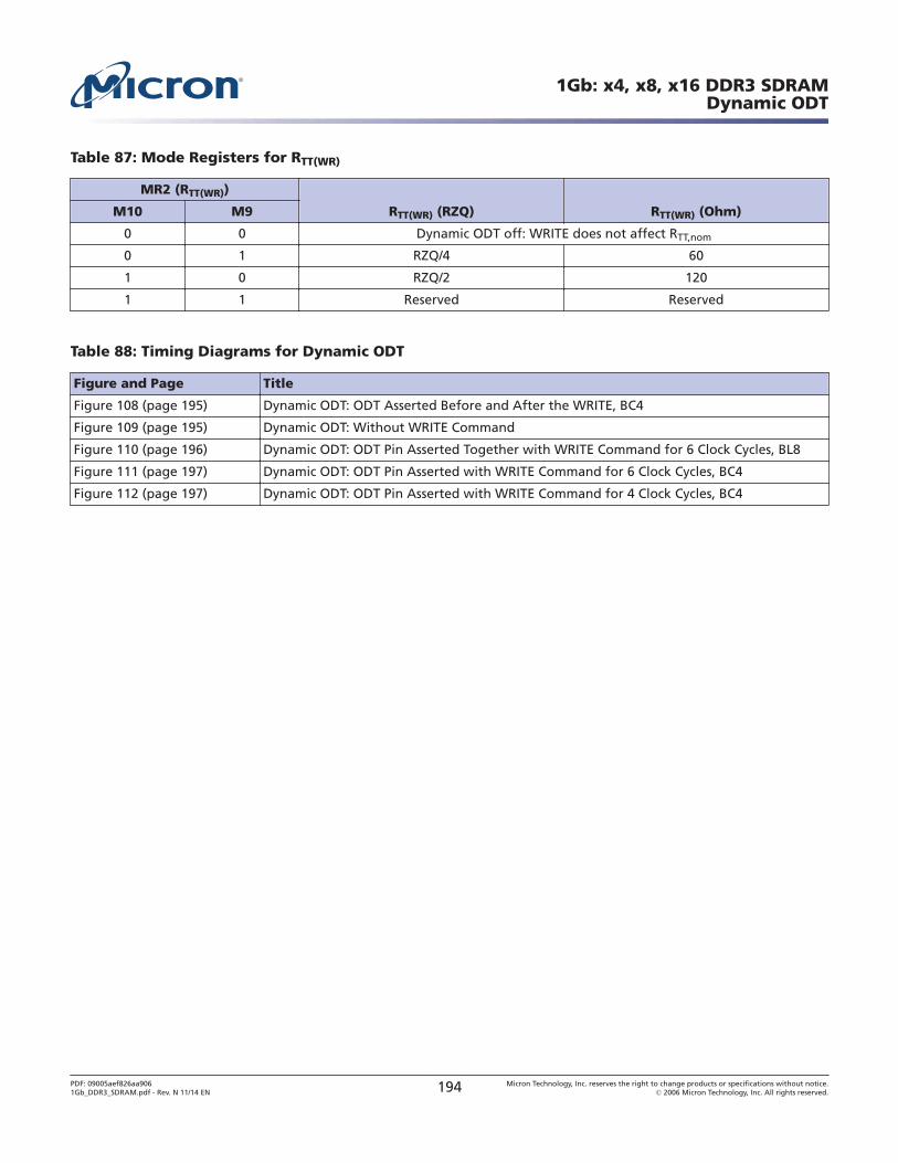
Table 87: Mode Registers for RTT(WR)
MR2 (RTT(WR))
RTT(WR) (RZQ) RTT(WR) (Ohm)M10 M9
0 0 Dynamic ODT off: WRITE does not affect RTT,nom
0 1 RZQ/4 60
1 0 RZQ/2 120
1 1 Reserved Reserved
Table 88: Timing Diagrams for Dynamic ODT
Figure and Page Title
Figure 108 (page 195) Dynamic ODT: ODT Asserted Before and After the WRITE, BC4
Figure 109 (page 195) Dynamic ODT: Without WRITE Command
Figure 110 (page 196) Dynamic ODT: ODT Pin Asserted Together with WRITE Command for 6 Clock Cycles, BL8
Figure 111 (page 197) Dynamic ODT: ODT Pin Asserted with WRITE Command for 6 Clock Cycles, BC4
Figure 112 (page 197) Dynamic ODT: ODT Pin Asserted with WRITE Command for 4 Clock Cycles, BC4
1Gb: x4, x8, x16 DDR3 SDRAMDynamic ODT
PDF: 09005aef826aa9061Gb_DDR3_SDRAM.pdf - Rev. N 11/14 EN 194 Micron Technology, Inc. reserves the right to change products or specifications without notice.
© 2006 Micron Technology, Inc. All rights reserved.
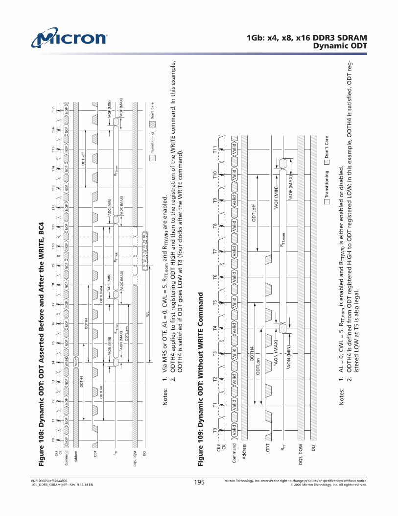
Fig
ure
10
8: D
yn
am
ic O
DT:
OD
T A
ssert
ed
Befo
re a
nd
Aft
er
the W
RIT
E, B
C4
T0T1
T2T3
T4T5
T6T7
T8T9
OD
TLo
nO
DTL
cwn
4
OD
TLcn
w
WL
OD
TLo
ff
T10
T11
T12
T13
T14
T15
T17
T16
CKCK#
Com
man
d
Add
ress
R TT
OD
T
DQ
DQ
S, D
QS#
Valid
WRS
4N
OP
NO
PN
OP
NO
PN
OP
NO
PN
OP
Do
n’t
Car
eTr
ansi
tio
nin
g
R TT(W
R)R TT
,nom
R TT,n
om
DI
n +
3D
In
+ 2
DI
n +
1D
I n
NO
PN
OP
NO
PN
OP
NO
PN
OP
NO
PN
OP
NO
PN
OP
OD
TH4
OD
TH4
t AO
N (
MIN
)t A
DC
(M
IN)
t AD
C (
MIN
)t A
OF
(MIN
)
t AO
N (
MA
X)
t AD
C (
MA
X)
t AD
C (
MA
X)
t AO
F (M
AX
)
No
tes:
1.V
ia M
RS
or
OTF
. AL
= 0
, CW
L =
5. R
TT,n
om
an
d R
TT(W
R) a
re e
nab
led
.2.
OD
TH4
app
lies
to f
irst
reg
iste
rin
g O
DT
HIG
H a
nd
th
en t
o t
he
reg
istr
atio
n o
f th
e W
RIT
E co
mm
and
. In
th
is e
xam
ple
,O
DTH
4 is
sat
isfi
ed if
OD
T g
oes
LO
W a
t T8
(fo
ur
clo
cks
afte
r th
e W
RIT
E co
mm
and
).
Fig
ure
10
9: D
yn
am
ic O
DT:
Wit
ho
ut
WR
ITE C
om
man
d
T0T1
T2T3
T4T5
T6T7
T8T9
OD
TLo
ff
T10
T11
CKCK#
R TT
Do
n’t
Car
eTr
ansi
tio
nin
g
Com
man
dV
alid
Val
idV
alid
Val
idV
alid
Val
idV
alid
Val
idV
alid
Val
idV
alid
Val
id
Add
ress
DQ
S, D
QS#
DQ
OD
TH4
OD
TLo
n
t AO
N (
MA
X)
t AO
N (
MIN
)
t AO
F (M
IN)
t AO
F (M
AX
)
OD
T
R TT,n
om
No
tes:
1.A
L =
0, C
WL
= 5
. RTT
,no
m is
en
able
d a
nd
RTT
(WR
) is
eith
er e
nab
led
or
dis
able
d.
2.O
DTH
4 is
def
ined
fro
m O
DT
reg
iste
red
HIG
H t
o O
DT
reg
iste
red
LO
W; i
n t
his
exa
mp
le, O
DTH
4 is
sat
isfi
ed. O
DT
reg
-is
tere
d L
OW
at
T5 is
als
o le
gal
.
1Gb: x4, x8, x16 DDR3 SDRAMDynamic ODT
PDF: 09005aef826aa9061Gb_DDR3_SDRAM.pdf - Rev. N 11/14 EN 195 Micron Technology, Inc. reserves the right to change products or specifications without notice.
© 2006 Micron Technology, Inc. All rights reserved.
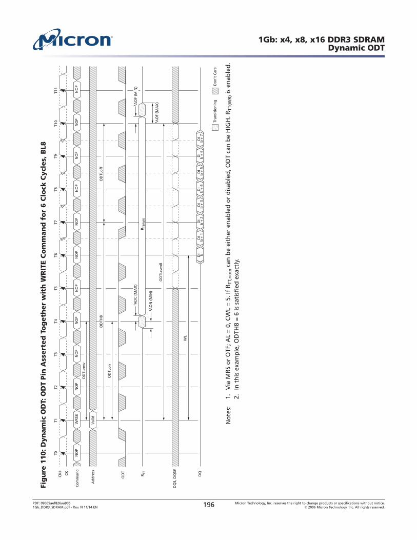
Fig
ure
11
0: D
yn
am
ic O
DT:
OD
T Pin
Ass
ert
ed
To
geth
er
wit
h W
RIT
E C
om
man
d f
or
6 C
lock
Cycl
es,
BL8
T0T1
T2T3
T4T5
T6T7
T8T9
OD
TLcw
n8
OD
TLo
n
OD
TLcn
w
WL
t AO
F (M
AX
)
T10
T11
CK
CK
#
Ad
dre
ss
R TT
OD
T
DQ
DQ
S, D
QS#
DI
b +
3D
Ib
+ 2
DI
b +
1D
I bD
Ib
+ 7
DI
b +
6D
Ib
+ 5
DI
b +
4
Val
id
Do
n’t
Car
eTr
ansi
tio
nin
g
Co
mm
and
WR
S8N
OP
NO
PN
OP
NO
PN
OP
NO
PN
OP
NO
PN
OP
NO
PN
OP
R TT(
WR
)
OD
TH8
OD
TLo
ff
t AD
C (
MA
X)
t AO
N (
MIN
)
t AO
F (M
IN)
No
tes:
1.V
ia M
RS
or
OTF
; AL
= 0
, CW
L =
5. I
f R
TT,n
om
can
be
eith
er e
nab
led
or
dis
able
d, O
DT
can
be
HIG
H. R
TT(W
R) i
s en
able
d.
2.In
th
is e
xam
ple
, OD
TH8
= 6
is s
atis
fied
exa
ctly
.
1Gb: x4, x8, x16 DDR3 SDRAMDynamic ODT
PDF: 09005aef826aa9061Gb_DDR3_SDRAM.pdf - Rev. N 11/14 EN 196 Micron Technology, Inc. reserves the right to change products or specifications without notice.
© 2006 Micron Technology, Inc. All rights reserved.
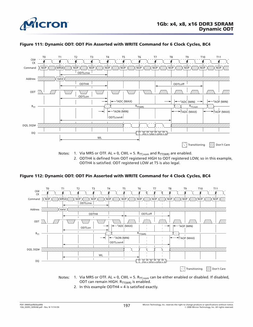
Figure 111: Dynamic ODT: ODT Pin Asserted with WRITE Command for 6 Clock Cycles, BC4
T0 T1 T2 T3 T4 T5 T6 T7 T8 T9
ODTLon
ODTLcnw
WL
T10 T11
CKCK#
ODTLcwn4
DQS, DQS#
Address Valid
Don’t CareTransitioning
ODTLoff
Command WRS4NOP NOPNOP NOP NOP NOP NOP NOP NOP NOP NOP
DQ DIn + 3
DIn + 2
DIn + 1
DIn
tADC (MIN) tAOF (MIN)
tAOF (MAX)tADC (MAX)
tADC (MAX)
tAON (MIN)
ODTH4
ODT
RTT RTT(WR) RTT,nom
Notes: 1. Via MRS or OTF. AL = 0, CWL = 5. RTT,nom and RTT(WR) are enabled.2. ODTH4 is defined from ODT registered HIGH to ODT registered LOW, so in this example,
ODTH4 is satisfied. ODT registered LOW at T5 is also legal.
Figure 112: Dynamic ODT: ODT Pin Asserted with WRITE Command for 4 Clock Cycles, BC4
T0 T1 T2 T3 T4 T5 T6 T7 T8 T9
ODTLon
ODTLcnw
WL
T10 T11
CKCK#
ODTLcwn4
DQS, DQS#
Address Valid
Command WRS4NOP NOPNOP NOP NOP NOP NOP NOP NOP NOP NOP
Don’t CareTransitioning
DQ DIn
DIn + 3
DIn + 2
DIn + 1
ODTH4
tADC (MAX)
tAON (MIN)
tAOF (MIN)
tAOF (MAX)
ODTLoff
RTT RTT(WR)
ODT
Notes: 1. Via MRS or OTF. AL = 0, CWL = 5. RTT,nom can be either enabled or disabled. If disabled,ODT can remain HIGH. RTT(WR) is enabled.
2. In this example ODTH4 = 4 is satisfied exactly.
1Gb: x4, x8, x16 DDR3 SDRAMDynamic ODT
PDF: 09005aef826aa9061Gb_DDR3_SDRAM.pdf - Rev. N 11/14 EN 197 Micron Technology, Inc. reserves the right to change products or specifications without notice.
© 2006 Micron Technology, Inc. All rights reserved.
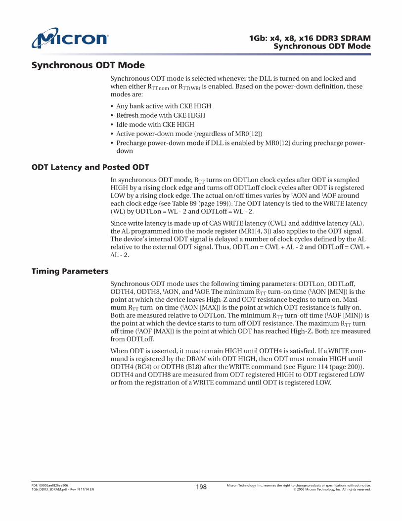
Synchronous ODT ModeSynchronous ODT mode is selected whenever the DLL is turned on and locked andwhen either RTT,nom or RTT(WR) is enabled. Based on the power-down definition, thesemodes are:
• Any bank active with CKE HIGH• Refresh mode with CKE HIGH• Idle mode with CKE HIGH• Active power-down mode (regardless of MR0[12])• Precharge power-down mode if DLL is enabled by MR0[12] during precharge power-
down
ODT Latency and Posted ODT
In synchronous ODT mode, RTT turns on ODTLon clock cycles after ODT is sampledHIGH by a rising clock edge and turns off ODTLoff clock cycles after ODT is registeredLOW by a rising clock edge. The actual on/off times varies by tAON and tAOF aroundeach clock edge (see Table 89 (page 199)). The ODT latency is tied to the WRITE latency(WL) by ODTLon = WL - 2 and ODTLoff = WL - 2.
Since write latency is made up of CAS WRITE latency (CWL) and additive latency (AL),the AL programmed into the mode register (MR1[4, 3]) also applies to the ODT signal.The device’s internal ODT signal is delayed a number of clock cycles defined by the ALrelative to the external ODT signal. Thus, ODTLon = CWL + AL - 2 and ODTLoff = CWL +AL - 2.
Timing Parameters
Synchronous ODT mode uses the following timing parameters: ODTLon, ODTLoff,ODTH4, ODTH8, tAON, and tAOF. The minimum RTT turn-on time (tAON [MIN]) is thepoint at which the device leaves High-Z and ODT resistance begins to turn on. Maxi-mum RTT turn-on time (tAON [MAX]) is the point at which ODT resistance is fully on.Both are measured relative to ODTLon. The minimum RTT turn-off time (tAOF [MIN]) isthe point at which the device starts to turn off ODT resistance. The maximum RTT turnoff time (tAOF [MAX]) is the point at which ODT has reached High-Z. Both are measuredfrom ODTLoff.
When ODT is asserted, it must remain HIGH until ODTH4 is satisfied. If a WRITE com-mand is registered by the DRAM with ODT HIGH, then ODT must remain HIGH untilODTH4 (BC4) or ODTH8 (BL8) after the WRITE command (see Figure 114 (page 200)).ODTH4 and ODTH8 are measured from ODT registered HIGH to ODT registered LOWor from the registration of a WRITE command until ODT is registered LOW.
1Gb: x4, x8, x16 DDR3 SDRAMSynchronous ODT Mode
PDF: 09005aef826aa9061Gb_DDR3_SDRAM.pdf - Rev. N 11/14 EN 198 Micron Technology, Inc. reserves the right to change products or specifications without notice.
© 2006 Micron Technology, Inc. All rights reserved.
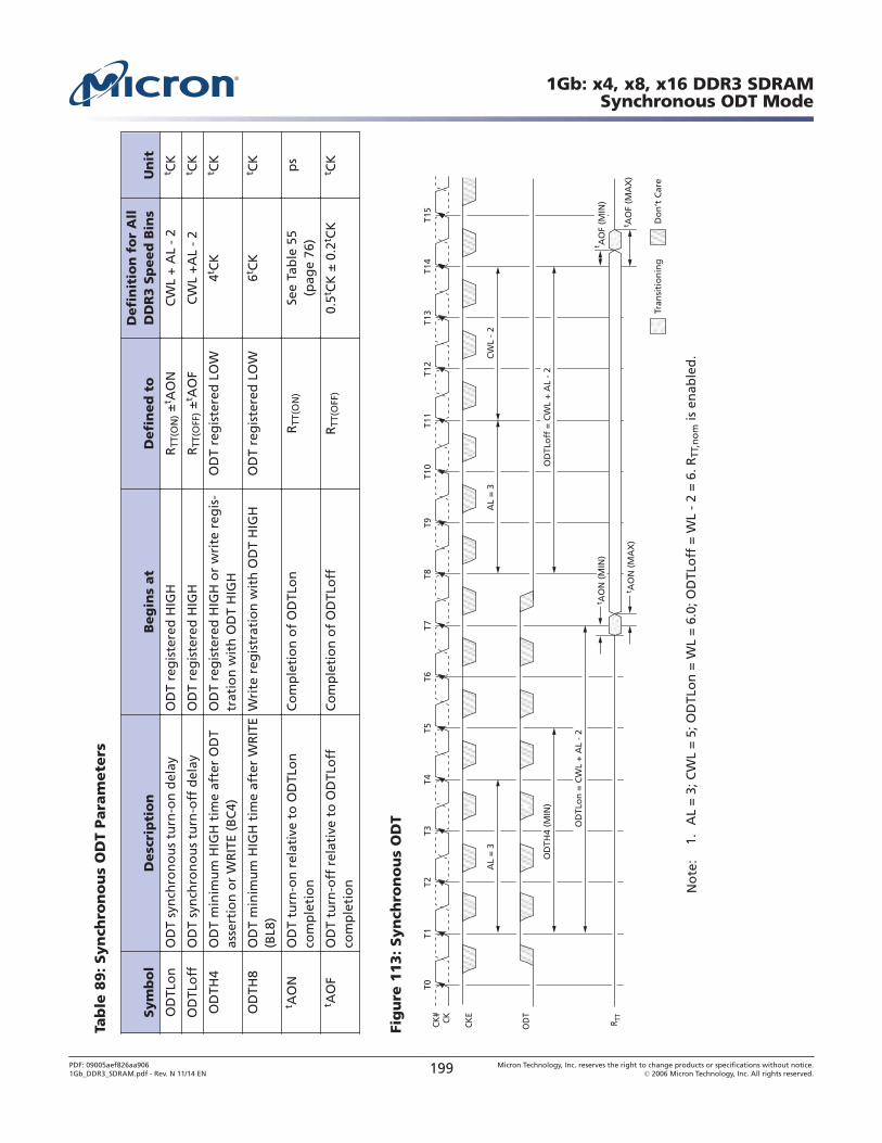
Tab
le 8
9: Syn
chro
no
us
OD
T Para
mete
rs
Sym
bo
lD
esc
rip
tio
nB
eg
ins
at
Defi
ned
to
Defi
nit
ion
fo
r A
llD
DR
3 S
peed
Bin
sU
nit
OD
TLo
nO
DT
syn
chro
no
us
turn
-on
del
ayO
DT
reg
iste
red
HIG
HR
TT(O
N) ±
t AO
NC
WL
+ A
L -
2t C
K
OD
TLo
ffO
DT
syn
chro
no
us
turn
-off
del
ayO
DT
reg
iste
red
HIG
HR
TT(O
FF) ±
t AO
FC
WL
+A
L -
2t C
K
OD
TH4
OD
T m
inim
um
HIG
H t
ime
afte
r O
DT
asse
rtio
n o
r W
RIT
E (B
C4)
OD
T re
gis
tere
d H
IGH
or
wri
te r
egis
-tr
atio
n w
ith
OD
T H
IGH
OD
T re
gis
tere
d L
OW
4t CK
t CK
OD
TH8
OD
T m
inim
um
HIG
H t
ime
afte
r W
RIT
E(B
L8)
Wri
te r
egis
trat
ion
wit
h O
DT
HIG
HO
DT
reg
iste
red
LO
W6t C
Kt C
K
t AO
NO
DT
turn
-on
rel
ativ
e to
OD
TLo
nco
mp
leti
on
Co
mp
leti
on
of
OD
TLo
nR
TT(O
N)
See
Tab
le 5
5(p
age
76)
ps
t AO
FO
DT
turn
-off
rel
ativ
e to
OD
TLo
ffco
mp
leti
on
Co
mp
leti
on
of
OD
TLo
ffR
TT(O
FF)
0.5t C
K ±
0.2
t CK
t CK
Fig
ure
11
3: Syn
chro
no
us
OD
T
T0T1
T2T3
T4T5
T6T7
T8T9
CW
L -
2A
L =
3A
L =
3
t AO
N (
MA
X)
t AO
F (M
AX
)
T10
T11
T12
T13
T14
T15
CKCK#
R TT
OD
T
Do
n’t
Car
eTr
ansi
tio
nin
g
R TT,n
om
CKE
t AO
F (M
IN)
OD
TLo
ff =
CW
L +
AL
- 2
OD
TLo
n =
CW
L +
AL
- 2
OD
TH4
(MIN
)
t AO
N (
MIN
)
No
te:
1.A
L =
3; C
WL
= 5
; OD
TLo
n =
WL
= 6
.0; O
DTL
off
= W
L -
2 =
6. R
TT,n
om
is e
nab
led
.
1Gb: x4, x8, x16 DDR3 SDRAMSynchronous ODT Mode
PDF: 09005aef826aa9061Gb_DDR3_SDRAM.pdf - Rev. N 11/14 EN 199 Micron Technology, Inc. reserves the right to change products or specifications without notice.
© 2006 Micron Technology, Inc. All rights reserved.
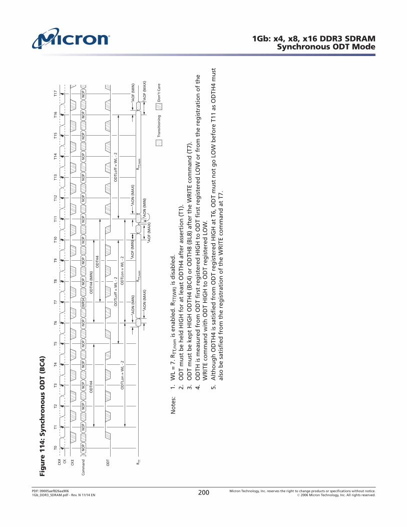
Fig
ure
11
4: Syn
chro
no
us
OD
T (B
C4)
T0T1
T2T3
T4T5
T6T7
T8T9
t AO
F (M
AX
)
t AO
F (M
IN)
t AO
N (
MA
X)
t AO
F (M
AX
)
T10
T11
T12
T13
T14
T15
T17
T16
CKCK#
R TT
CKE
NO
PW
RS4
NO
PN
OP
NO
PN
OP
NO
PN
OP
NO
PN
OP
NO
PN
OP
NO
PN
OP
NO
PN
OP
NO
PN
OP
Com
man
d
Do
n’t
Car
eTr
ansi
tio
nin
g
t AO
N (
MIN
)
R TT,n
om
OD
TLo
ff =
WL
- 2
OD
TH4
(MIN
) O
DTH
4
OD
TLo
ff =
WL
- 2
OD
TLo
n =
WL
- 2
t AO
N (
MIN
)t A
ON
(M
AX
)
OD
TH4
OD
TLo
n =
WL
- 2
t AO
F (M
IN)
OD
T
R TT,n
om
No
tes:
1.W
L =
7. R
TT,n
om
is e
nab
led
. RTT
(WR
) is
dis
able
d.
2.O
DT
mu
st b
e h
eld
HIG
H f
or
at le
ast
OD
TH4
afte
r as
sert
ion
(T1
).3.
OD
T m
ust
be
kep
t H
IGH
OD
TH4
(BC
4) o
r O
DTH
8 (B
L8)
afte
r th
e W
RIT
E co
mm
and
(T7
).4.
OD
TH is
mea
sure
d f
rom
OD
T fi
rst
reg
iste
red
HIG
H t
o O
DT
firs
t re
gis
tere
d L
OW
or
fro
m t
he
reg
istr
atio
n o
f th
eW
RIT
E co
mm
and
wit
h O
DT
HIG
H t
o O
DT
reg
iste
red
LO
W.
5.A
lth
ou
gh
OD
TH4
is s
atis
fied
fro
m O
DT
reg
iste
red
HIG
H a
t T6
, OD
T m
ust
no
t g
o L
OW
bef
ore
T11
as
OD
TH4
mu
stal
so b
e sa
tisf
ied
fro
m t
he
reg
istr
atio
n o
f th
e W
RIT
E co
mm
and
at
T7.
1Gb: x4, x8, x16 DDR3 SDRAMSynchronous ODT Mode
PDF: 09005aef826aa9061Gb_DDR3_SDRAM.pdf - Rev. N 11/14 EN 200 Micron Technology, Inc. reserves the right to change products or specifications without notice.
© 2006 Micron Technology, Inc. All rights reserved.
ODT Off During READs
Because the device cannot terminate and drive at the same time, RTT must be disabledat least one-half clock cycle before the READ preamble by driving the ODT ball LOW (ifeither RTT,nom or RTT(WR) is enabled). RTT may not be enabled until the end of the post-amble, as shown in the following example.Note: ODT may be disabled earlier and enabled later than shown in Figure 115(page 202).
1Gb: x4, x8, x16 DDR3 SDRAMSynchronous ODT Mode
PDF: 09005aef826aa9061Gb_DDR3_SDRAM.pdf - Rev. N 11/14 EN 201 Micron Technology, Inc. reserves the right to change products or specifications without notice.
© 2006 Micron Technology, Inc. All rights reserved.
Fig
ure
11
5: O
DT
Du
rin
g R
EA
Ds
T0
T1T2
T3T4
T5T6
T7T8
T9T1
0T1
1T1
2T1
3T1
4T1
5T1
7T1
6
CKCK#
Valid
Add
ress
DI
b +
3D
Ib
+ 2
DI
b +
1D
I bD
Ib
+ 7
DI
b +
6D
Ib
+ 5
DI
b +
4D
Q
DQ
S, D
QS#
Do
n’t
Car
eTr
ansi
tio
nin
g
Com
man
dN
OP
NO
PN
OP
NO
PN
OP
NO
PN
OP
NO
PN
OP
NO
PN
OP
NO
PN
OP
NO
PN
OP
NO
PN
OP
REA
D
OD
TLo
n =
CW
L +
AL
- 2
OD
T
t AO
N (
MA
X)
RL
= A
L +
CL
OD
TLo
ff =
CW
L +
AL
- 2
t AO
F (M
IN)
R TTR TT
,nom
R TT,n
omt A
OF
(MA
X)
No
te:
1.O
DT
mu
st b
e d
isab
led
ext
ern
ally
du
rin
g R
EAD
s b
y d
rivi
ng
OD
T LO
W. F
or
exam
ple
, CL
= 6
; AL
= C
L -
1 =
5; R
L =
AL
+ C
L =
11;
CW
L =
5; O
DTL
on
= C
WL
+ A
L -
2 =
8; O
DTL
off
= C
WL
+ A
L -
2 =
8. R
TT,n
om
is e
nab
led
. RTT
(WR
) is
a “D
on
’tC
are.
”
1Gb: x4, x8, x16 DDR3 SDRAMSynchronous ODT Mode
PDF: 09005aef826aa9061Gb_DDR3_SDRAM.pdf - Rev. N 11/14 EN 202 Micron Technology, Inc. reserves the right to change products or specifications without notice.
© 2006 Micron Technology, Inc. All rights reserved.
Asynchronous ODT ModeAsynchronous ODT mode is available when the DRAM runs in DLL on mode and wheneither RTT,nom or RTT(WR) is enabled; however, the DLL is temporarily turned off in pre-charged power-down standby (via MR0[12]). Additionally, ODT operates asynchronous-ly when the DLL is synchronizing after being reset. See Power-Down Mode (page 180)for definition and guidance over power-down details.
In asynchronous ODT timing mode, the internal ODT command is not delayed by ALrelative to the external ODT command. In asynchronous ODT mode, ODT controls RTTby analog time. The timing parameters tAONPD and tAOFPD replace ODTLon/tAONand ODTLoff/tAOF, respectively, when ODT operates asynchronously.
The minimum RTT turn-on time (tAONPD [MIN]) is the point at which the device termi-nation circuit leaves High-Z and ODT resistance begins to turn on. Maximum RTT turn-on time (tAONPD [MAX]) is the point at which ODT resistance is fully on. tAONPD(MIN) and tAONPD (MAX) are measured from ODT being sampled HIGH.
The minimum RTT turn-off time (tAOFPD [MIN]) is the point at which the device termi-nation circuit starts to turn off ODT resistance. Maximum RTT turn-off time (tAOFPD[MAX]) is the point at which ODT has reached High-Z. tAOFPD (MIN) and tAOFPD(MAX) are measured from ODT being sampled LOW.
1Gb: x4, x8, x16 DDR3 SDRAMAsynchronous ODT Mode
PDF: 09005aef826aa9061Gb_DDR3_SDRAM.pdf - Rev. N 11/14 EN 203 Micron Technology, Inc. reserves the right to change products or specifications without notice.
© 2006 Micron Technology, Inc. All rights reserved.
Fig
ure
11
6: A
syn
chro
no
us
OD
T Ti
min
g w
ith
Fast
OD
T Tr
an
siti
on
T0T1
T2T3
T4T5
T6T7
T8T9
t AO
NPD
(M
AX
)t A
OFP
D (
MA
X)
T10
T11
T12
T13
T14
T15
T17
T16
CKCK#
R TT
OD
T
R TT,n
om
Do
n’t
Car
eTr
ansi
tio
nin
g
CKE
t IHt IS
t IHt IS
t AO
FPD
(M
IN)
t AO
NPD
(M
IN)
No
te:
1.A
L is
ign
ore
d.
Tab
le 9
0: A
syn
chro
no
us
OD
T Ti
min
g P
ara
mete
rs f
or
All
Sp
eed
Bin
s
Sym
bo
lD
esc
rip
tio
nM
inM
ax
Un
itt A
ON
PDA
syn
chro
no
us
RTT
tu
rn-o
n d
elay
(p
ow
er-d
ow
n w
ith
DLL
off
)2
8.5
ns
t AO
FPD
Asy
nch
ron
ou
s R
TT t
urn
-off
del
ay (
po
wer
-do
wn
wit
h D
LL o
ff)
28.
5n
s
1Gb: x4, x8, x16 DDR3 SDRAMAsynchronous ODT Mode
PDF: 09005aef826aa9061Gb_DDR3_SDRAM.pdf - Rev. N 11/14 EN 204 Micron Technology, Inc. reserves the right to change products or specifications without notice.
© 2006 Micron Technology, Inc. All rights reserved.
Synchronous to Asynchronous ODT Mode Transition (Power-Down Entry)
There is a transition period around power-down entry (PDE) where the DRAM’s ODTmay exhibit either synchronous or asynchronous behavior. This transition period oc-curs if the DLL is selected to be off when in precharge power-down mode by the settingMR0[12] = 0. Power-down entry begins tANPD prior to CKE first being registered LOW,and ends when CKE is first registered LOW. tANPD is equal to the greater of ODTLoff +1tCK or ODTLon + 1tCK. If a REFRESH command has been issued, and it is in progresswhen CKE goes LOW, power-down entry ends tRFC after the REFRESH command, rath-er than when CKE is first registered LOW. Power-down entry then becomes the greaterof tANPD and tRFC - REFRESH command to CKE registered LOW.
ODT assertion during power-down entry results in an RTT change as early as the lesserof tAONPD (MIN) and ODTLon × tCK + tAON (MIN), or as late as the greater of tAONPD(MAX) and ODTLon × tCK + tAON (MAX). ODT de-assertion during power-down entrycan result in an RTT change as early as the lesser of tAOFPD (MIN) and ODTLoff × tCK +tAOF (MIN), or as late as the greater of tAOFPD (MAX) and ODTLoff × tCK + tAOF (MAX).Table 91 (page 206) summarizes these parameters.
If AL has a large value, the uncertainty of the state of RTT becomes quite large. This isbecause ODTLon and ODTLoff are derived from the WL; and WL is equal to CWL + AL.Figure 117 (page 206) shows three different cases:
• ODT_A: Synchronous behavior before tANPD.• ODT_B: ODT state changes during the transition period with tAONPD (MIN) <
ODTLon × tCK + tAON (MIN) and tAONPD (MAX) > ODTLon × tCK + tAON (MAX).• ODT_C: ODT state changes after the transition period with asynchronous behavior.
1Gb: x4, x8, x16 DDR3 SDRAMAsynchronous ODT Mode
PDF: 09005aef826aa9061Gb_DDR3_SDRAM.pdf - Rev. N 11/14 EN 205 Micron Technology, Inc. reserves the right to change products or specifications without notice.
© 2006 Micron Technology, Inc. All rights reserved.
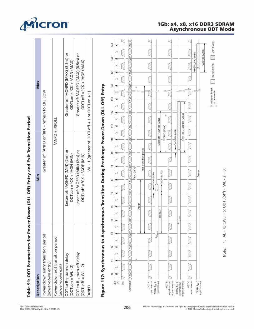
Tab
le 9
1: O
DT
Para
mete
rs f
or
Po
wer-
Do
wn
(D
LL O
ff)
En
try a
nd
Exit
Tra
nsi
tio
n P
eri
od
Desc
rip
tio
nM
inM
ax
Pow
er-d
ow
n e
ntr
y tr
ansi
tio
n p
erio
d(p
ow
er-d
ow
n e
ntr
y)G
reat
er o
f: t A
NPD
or
t RFC
- r
efre
sh t
o C
KE
LOW
Pow
er-d
ow
n e
xit
tran
siti
on
per
iod
(po
wer
-do
wn
exi
t)
t AN
PD +
t XPD
LL
OD
T to
RTT
tu
rn-o
n d
elay
(OD
TLo
n =
WL
- 2)
Less
er o
f: t A
ON
PD (
MIN
) (2
ns)
or
OD
TLo
n ×
t CK
+ t A
ON
(M
IN)
Gre
ater
of:
t AO
NPD
(M
AX
) (8
.5n
s) o
rO
DTL
on
× t C
K +
t AO
N (
MA
X)
OD
T to
RTT
tu
rn-o
ff d
elay
(OD
TLo
ff =
WL
- 2)
Less
er o
f: t A
OFP
D (
MIN
) (2
ns)
or
OD
TLo
ff ×
t CK
+ t A
OF
(MIN
)G
reat
er o
f: t A
OFP
D (
MA
X)
(8.5
ns)
or
OD
TLo
ff ×
t CK
+ t A
OF
(MA
X)
t AN
PDW
L -
1 (g
reat
er o
f O
DTL
off
+ 1
or
OD
TLo
n +
1)
Fig
ure
11
7: Syn
chro
no
us
to A
syn
chro
no
us
Tran
siti
on
Du
rin
g P
rech
arg
e P
ow
er-
Do
wn
(D
LL O
ff)
En
try
T0T1
T2T3
T4T5
T6T7
T8T9
t AO
FPD
(M
AX
)
OD
TLo
ff
T10
T11
T12
T13
Ta0
Ta1
Ta3
Ta2
CKCK#
DRA
M R
TT B
as
ynch
rono
us
or s
ynch
rono
us
R TT,n
om
DRA
M R
TT C
asyn
chro
nous
R TT,n
om
Do
n’t
Car
eTr
ansi
tio
nin
g
CKE
NO
PN
OP
NO
PN
OP
NO
PCo
mm
and
NO
PRE
FN
OP
NO
PN
OP
NO
PN
OP
NO
PN
OP
NO
PN
OP
NO
PN
OP
PDE
tran
siti
on
per
iod
Ind
icat
es b
reak
in t
ime
scal
e
OD
TLo
ff +
tA
OFP
D (
MIN
)
t AO
FPD
(M
AX
)
t AO
FPD
(M
IN)
OD
TLo
ff +
t AO
FPD
(M
AX
)
t AO
FPD
(M
IN)
t AN
PD
t AO
F (M
IN)
t AO
F (M
AX
)
DRA
M R
TT A
sy
nchr
onou
sR TT
,nom
OD
T A
sy
nchr
onou
s
OD
T C
asyn
chro
nous
OD
T B
asyn
chro
nous
or
syn
chro
nous
t RFC
(M
IN)
No
te:
1.A
L =
0; C
WL
= 5
; OD
TL(o
ff)
= W
L -
2 =
3.
1Gb: x4, x8, x16 DDR3 SDRAMAsynchronous ODT Mode
PDF: 09005aef826aa9061Gb_DDR3_SDRAM.pdf - Rev. N 11/14 EN 206 Micron Technology, Inc. reserves the right to change products or specifications without notice.
© 2006 Micron Technology, Inc. All rights reserved.
Asynchronous to Synchronous ODT Mode Transition (Power-Down Exit)The DRAM’s ODT can exhibit either asynchronous or synchronous behavior duringpower-down exit (PDX). This transition period occurs if the DLL is selected to be offwhen in precharge power-down mode by setting MR0[12] to 0. Power-down exit beginstANPD prior to CKE first being registered HIGH, and ends tXPDLL after CKE is first reg-istered HIGH. tANPD is equal to the greater of ODTLoff + 1tCK or ODTLon + 1tCK. Thetransition period is tANPD + tXPDLL.
ODT assertion during power-down exit results in an RTT change as early as the lesser oftAONPD (MIN) and ODTLon × tCK + tAON (MIN), or as late as the greater of tAONPD(MAX) and ODTLon × tCK + tAON (MAX). ODT de-assertion during power-down exitmay result in an RTT change as early as the lesser of tAOFPD (MIN) and ODTLoff × tCK +tAOF (MIN), or as late as the greater of tAOFPD (MAX) and ODTLoff × tCK + tAOF (MAX).Table 91 (page 206) summarizes these parameters.
If AL has a large value, the uncertainty of the RTT state becomes quite large. This is be-cause ODTLon and ODTLoff are derived from WL, and WL is equal to CWL + AL. Fig-ure 118 (page 208) shows three different cases:
• ODT C: Asynchronous behavior before tANPD.• ODT B: ODT state changes during the transition period, with tAOFPD (MIN) < ODTL-
off × tCK + tAOF (MIN), and ODTLoff × tCK + tAOF (MAX) > tAOFPD (MAX).• ODT A: ODT state changes after the transition period with synchronous response.
1Gb: x4, x8, x16 DDR3 SDRAMAsynchronous to Synchronous ODT Mode Transition (Power-
Down Exit)
PDF: 09005aef826aa9061Gb_DDR3_SDRAM.pdf - Rev. N 11/14 EN 207 Micron Technology, Inc. reserves the right to change products or specifications without notice.
© 2006 Micron Technology, Inc. All rights reserved.
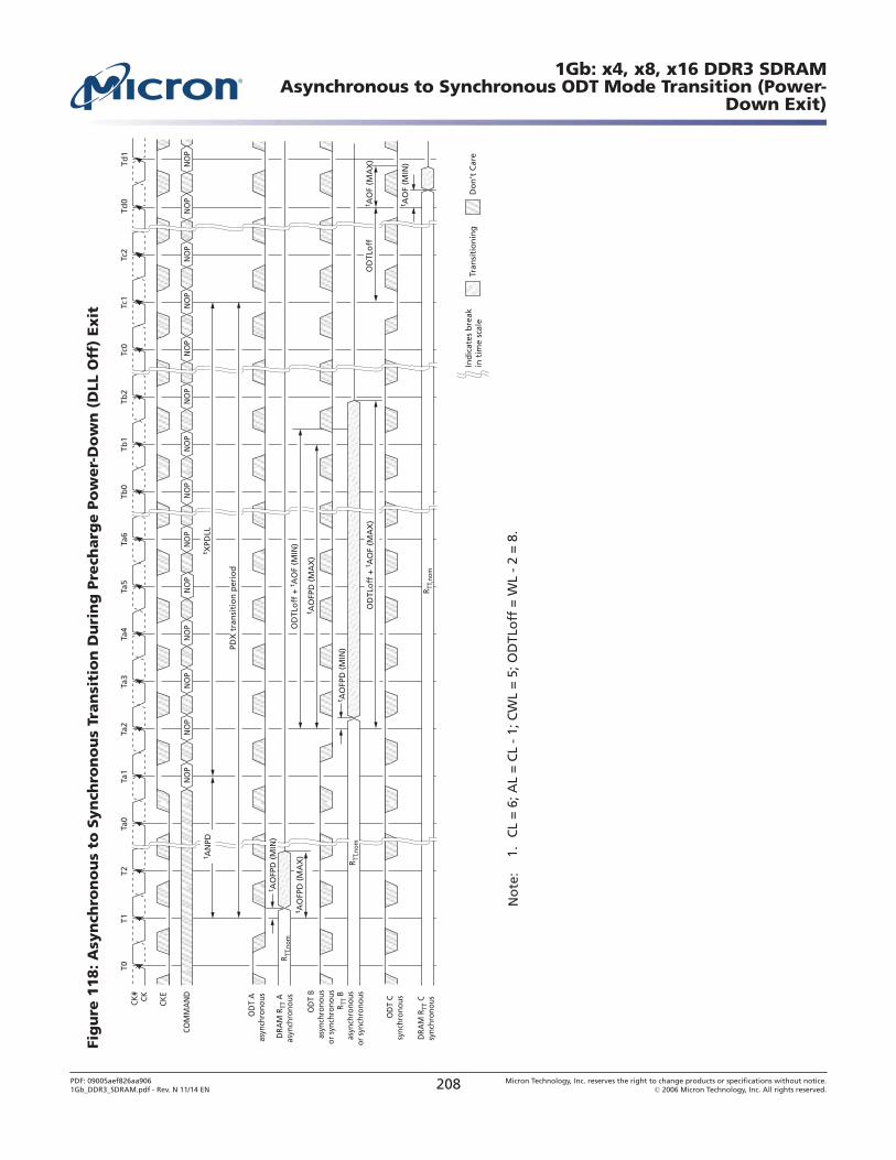
Fig
ure
11
8: A
syn
chro
no
us
to S
yn
chro
no
us
Tran
siti
on
Du
rin
g P
rech
arg
e P
ow
er-
Do
wn
(D
LL O
ff)
Exit
T0T1
T2Ta
0Ta
1Ta
2Ta
3Ta
4Ta
5Ta
6Tb
0Tb
1Tb
2Tc
0Tc
1Td
0Td
1Tc
2
CKCK#
Do
n’t
Car
eTr
ansi
tio
nin
g
OD
T C
sync
hron
ous
NO
PN
OP
NO
PCO
MM
AN
DN
OP
NO
PN
OP
NO
PN
OP
NO
PN
OP
NO
PN
OP
R TT B
asyn
chro
nous
or s
ynch
rono
us
DRA
M R
TT A
asyn
chro
nous
DRA
M R
TT C
sync
hron
ous
R TT,n
om
NO
PN
OP
OD
T B
asyn
chro
nous
or s
ynch
rono
us
CKE
t AO
F (M
IN)
R TT,n
om
Ind
icat
es b
reak
in t
ime
scal
e
OD
TLo
ff +
tA
OF
(MIN
)
t AO
FPD
(M
AX
)
OD
TLo
ff +
tA
OF
(MA
X)
t XPD
LL
t AO
F (M
AX
)O
DTL
off
OD
T A
asyn
chro
nous
PDX
tra
nsi
tio
n p
erio
d
t AO
FPD
(M
IN)
t AO
FPD
(M
AX
)
R TT,n
om
t AN
PD
t AO
FPD
(M
IN)
No
te:
1.C
L =
6; A
L =
CL
- 1;
CW
L =
5; O
DTL
off
= W
L -
2 =
8.
1Gb: x4, x8, x16 DDR3 SDRAMAsynchronous to Synchronous ODT Mode Transition (Power-
Down Exit)
PDF: 09005aef826aa9061Gb_DDR3_SDRAM.pdf - Rev. N 11/14 EN 208 Micron Technology, Inc. reserves the right to change products or specifications without notice.
© 2006 Micron Technology, Inc. All rights reserved.
Asynchronous to Synchronous ODT Mode Transition (Short CKE Pulse)
If the time in the precharge power-down or idle states is very short (short CKE LOWpulse), the power-down entry and power-down exit transition periods overlap. Whenoverlap occurs, the response of the DRAM’s RTT to a change in the ODT state can besynchronous or asynchronous from the start of the power-down entry transition periodto the end of the power-down exit transition period, even if the entry period ends laterthan the exit period.
If the time in the idle state is very short (short CKE HIGH pulse), the power-down exitand power-down entry transition periods overlap. When this overlap occurs, the re-sponse of the DRAM’s RTT to a change in the ODT state may be synchronous or asyn-chronous from the start of power-down exit transition period to the end of the power-down entry transition period.
1Gb: x4, x8, x16 DDR3 SDRAMAsynchronous to Synchronous ODT Mode Transition (Power-
Down Exit)
PDF: 09005aef826aa9061Gb_DDR3_SDRAM.pdf - Rev. N 11/14 EN 209 Micron Technology, Inc. reserves the right to change products or specifications without notice.
© 2006 Micron Technology, Inc. All rights reserved.
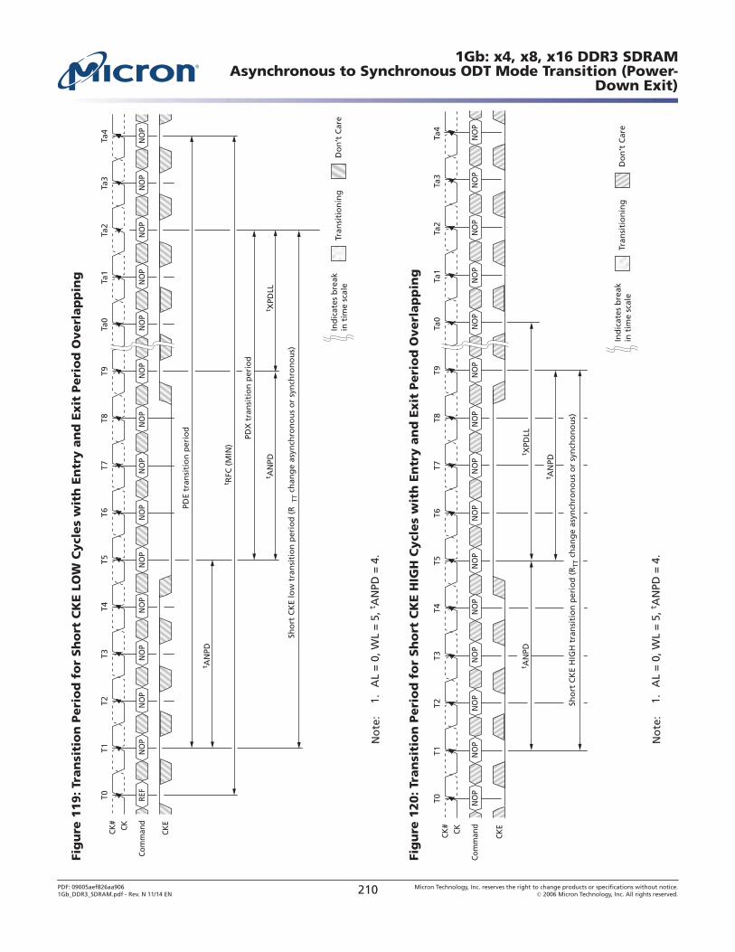
Fig
ure
11
9: Tr
an
siti
on
Peri
od
fo
r Sh
ort
CK
E L
OW
Cycl
es
wit
h E
ntr
y a
nd
Exit
Peri
od
Overl
ap
pin
g
T0T1
T2T3
T4T5
T6T7
T8T9
Ta0
Ta1
Ta2
Ta3
Ta4
CKCK#
CKE
Com
man
d
Do
n’t
Car
eTr
ansi
tio
nin
g
t XPD
LL
t RFC
(M
IN)
NO
PN
OP
NO
PN
OP
NO
PN
OP
NO
PN
OP
NO
PN
OP
REF
NO
PN
OP
NO
PN
OP
PDE
tran
siti
on
per
iod
PDX
tra
nsi
tio
n p
erio
d
Ind
icat
es b
reak
in t
ime
scal
e
t AN
PD
Sho
rt C
KE
low
tra
nsi
tio
n p
erio
d (
RTT
ch
ang
e as
ynch
ron
ou
s o
r sy
nch
ron
ou
s)
t AN
PD
No
te:
1.A
L =
0, W
L =
5, t A
NPD
= 4
.
Fig
ure
12
0: Tr
an
siti
on
Peri
od
fo
r Sh
ort
CK
E H
IGH
Cycl
es
wit
h E
ntr
y a
nd
Exit
Peri
od
Overl
ap
pin
g
T0T1
T2T3
T4T5
T6T7
T8T9
CKCK#
Com
man
d
Do
n’t
Car
eTr
ansi
tio
nin
g
NO
PN
OP
NO
PN
OP
NO
PN
OP
NO
PN
OP
NO
PN
OP
NO
PN
OP
NO
PN
OP
NO
PN
OP
t AN
PDt X
PDLL
Ind
icat
es b
reak
in t
ime
scal
e
Ta0
Ta1
Ta2
Ta3
Ta4
CKE
t AN
PD
Sho
rt C
KE
HIG
H t
ran
siti
on
per
iod
(R
TT c
han
ge
asyn
chro
no
us
or
syn
cho
no
us)
No
te:
1.A
L =
0, W
L =
5, t A
NPD
= 4
.
1Gb: x4, x8, x16 DDR3 SDRAMAsynchronous to Synchronous ODT Mode Transition (Power-
Down Exit)
PDF: 09005aef826aa9061Gb_DDR3_SDRAM.pdf - Rev. N 11/14 EN 210 Micron Technology, Inc. reserves the right to change products or specifications without notice.
© 2006 Micron Technology, Inc. All rights reserved.
8000 S. Federal Way, P.O. Box 6, Boise, ID 83707-0006, Tel: 208-368-4000www.micron.com/products/support Sales inquiries: 800-932-4992
Micron and the Micron logo are trademarks of Micron Technology, Inc.All other trademarks are the property of their respective owners.
This data sheet contains minimum and maximum limits specified over the power supply and temperature range set forth herein.Although considered final, these specifications are subject to change, as further product development and data characterization some-
times occur.
1Gb: x4, x8, x16 DDR3 SDRAMAsynchronous to Synchronous ODT Mode Transition (Power-
Down Exit)
PDF: 09005aef826aa9061Gb_DDR3_SDRAM.pdf - Rev. N 11/14 EN 211 Micron Technology, Inc. reserves the right to change products or specifications without notice.
© 2006 Micron Technology, Inc. All rights reserved.

![2Gb C-die DDR3 SDRAM Industrial€¦ · datasheet DDR3 SDRAM Rev. 1.0 K4B2G1646C Industrial 1. Ordering Information [ Table 1 ] Samsung 2Gb DDR3 C-die ordering information table NOTE:](https://static.fdocuments.in/doc/165x107/5ecc8b7cc35ff9103a633f0f/2gb-c-die-ddr3-sdram-datasheet-ddr3-sdram-rev-10-k4b2g1646c-industrial-1-ordering.jpg)


![AIMB-580 user manual ed.1 - Advantechadvdownload.advantech.com/productfile/Downloadfile3/1...ed[1].1.pdf · Tran-scend 1GB DDR3 1333 DDR3 N TS128MLK64V3U SEC 907 HCH9 K4B1G08460(128x8)](https://static.fdocuments.in/doc/165x107/5ab3bfd47f8b9a284c8eaab7/aimb-580-user-manual-ed1-11pdftran-scend-1gb-ddr3-1333-ddr3-n-ts128mlk64v3u.jpg)
![4Gb D-die DDR3 SDRAM- 5 - K4B4G0846D datasheet DDR3 SDRAM Rev. 1.23 K4B4G0446D 1. Ordering Information [ Table 1 ] Samsung 4Gb DDR3 D-die ordering information table NOTE: 1. Speed](https://static.fdocuments.in/doc/165x107/5e73e86eb6f1e10b075d492a/4gb-d-die-ddr3-sdram-5-k4b4g0846d-datasheet-ddr3-sdram-rev-123-k4b4g0446d.jpg)
![1Gb F-die DDR3 SDRAM...- 5 - K4B1G0846F datasheet DDR3 SDRAM Rev. 1.21 K4B1G0446F 1. Ordering Information [ Table 1 ] Samsung 1Gb DDR3 F-die ordering information table NOTE: 1. Speed](https://static.fdocuments.in/doc/165x107/6118fdb29861ea1e5e6a2225/1gb-f-die-ddr3-5-k4b1g0846f-datasheet-ddr3-sdram-rev-121-k4b1g0446f-1.jpg)

![96FBGA with Lead-Free & Halogen-Free · DDR3 SDRAM Addressing ... [ Table 47 ] DDR3-800 Speed Bins [ Table 48 ] DR3-1066 Speed Bins Parameter Symbol 1Gb 2Gb 4Gb 8Gb Units NOTE](https://static.fdocuments.in/doc/165x107/5ad5dbf67f8b9a5c638d9a8c/96fbga-with-lead-free-halogen-free-sdram-addressing-table-47-ddr3-800-speed.jpg)