1999 Behaviour of variable speed drives under the ...
158
University of Wollongong Research Online University of Wollongong esis Collection University of Wollongong esis Collections 1999 Behaviour of variable speed drives under the influence of voltage sags Rajagopalan Lakshmi Narayanan University of Wollongong Research Online is the open access institutional repository for the University of Wollongong. For further information contact Manager Repository Services: [email protected]. Recommended Citation Narayanan, Rajagopalan Lakshmi, Behaviour of variable speed drives under the influence of voltage sags, Master of Engineering (Hons.) thesis, School of Electrical, Computer and Telecommunications Engineering, University of Wollongong, 1999. hp://ro.uow.edu.au/theses/2544
Transcript of 1999 Behaviour of variable speed drives under the ...
University of WollongongResearch Online
University of Wollongong Thesis Collection University of Wollongong Thesis Collections
1999
Behaviour of variable speed drives under theinfluence of voltage sagsRajagopalan Lakshmi NarayananUniversity of Wollongong
Research Online is the open access institutional repository for theUniversity of Wollongong. For further information contact ManagerRepository Services: [email protected].
Recommended CitationNarayanan, Rajagopalan Lakshmi, Behaviour of variable speed drives under the influence of voltage sags, Master of Engineering(Hons.) thesis, School of Electrical, Computer and Telecommunications Engineering, University of Wollongong, 1999.http://ro.uow.edu.au/theses/2544

BEHAVIOUR OF VARIABLE SPEED DRIVES
UNDER THE INFLUENCE OF VOLTAGE SAGS
A thesis submitted in fulfilment of the requirements for the
award of the degree
MASTER OF ENGINEERING (HONOURS)
from
UNIVERSITY OF WOLLONGONG
by
RAJAGOPALAN LAKSHMI NARAYANAN (MEngStud)
SCHOOL OF ELECTRICAL, COMPUTER A N D TELECOMMUNICATIONS
ENGINEERING, 1999
11
CONTENTS
ACKNOWLEDGEMENTS vii
ABSTRACT viii
LIST OF SYMBOLS ix
CHAPTER 1 INTRODUCTION
1.1 Variable Speed Drives in Process Plants 1
1.2 Voltage Sags and their Causes 2
1.3 Types of Voltage Sags 3
1.4 Impact of Voltage Sags on VSDs 3
1.4.1 Impact of a Balanced Sag 4
1.4.2 Impact of an Unbalanced Sag 5
1.5 Conventional Mitigation Strategies 5
1.5.1 Mitigation Techniques by Hardware Modifications 6
1.5.2 Mitigation Techniques by Means of Improved
Power Supply Conditions 8
1.5.3 Mitigation Techniques by Control Algorithm Modifications 10
1.6 Aim of the Thesis 11
1.7 Contributions of this Thesis 12
1.8 Scope of Work and Plan of the Thesis 13
CHAPTER 2 PROPOSED CONTROL STRATEGY AND
MODELLING OF VSDs
2.1 Introduction 15
2.2 Proposed Control Strategy 16
2.2.1 Set Points for Control Strategy 17
2.2.2 Control Sequence and Flow Charting 18
2.3 Control Loops in A C VSDs Operating Under Field Orientation 20
2.3.1 Control Model of an IM V S D 21
2.3.2 Control Model of an S R M V S D 25

Ill
2.4 Proposed Additional Control Loops for D C Bus Voltage Control 26
2.4.1 Bus Voltage Control by Recovering Load Kinetic Energy 27
2.4.2 Bus Voltage Control by Recovering Magnetising Energy 29
2.5 Power Balance Between A C Supply, Bus Capacitor and A C Motor 31
2.5.1 Power Flow Between A C Supply and D C Bus Capacitor 31
2.5.2 Power Flow Between D C Bus Capacitor and A C Motor 32
2.6 Summary 34
CHAPTER 3 PERFORMANCE OF A SYNCHRONOUS
RELUCTANCE MOTOR DRIVE
3.1 Introduction 35
3.2 Sag Types Under Study 3 6
3.3 Normal Speed Control Operation of an S R M V S D 3 8
3.3.1 Performance Under Normal Operating Conditions - N o Sag 38
3.3.2 V S D Behaviour during a Voltage Sag 43
3.3.3 Reasons For V S D Tripping on a Sag Condition 47
3.4 Operation Under a Sag at High Speeds - Bus Voltage Control
by Recovering Kinetic Energy 49
3.5 Operation Under a Sag at Low Speeds - Bus Voltage Control
by Recovering Magnetising Energy 53
3.6 Coordinated V S D Control at all Speeds 55
3.7 Effect of Lowering the Bus Capacitance 57
3.8 Summary 60
CHAPTER 4 PERFORMANCE OF AN INDUCTION MOTOR DRIVE
4.1 Introduction 61
4.2 Normal Speed Control Operation of an IM V S D 62
4.2.1 Performance Under Normal Operating Conditions - N o Sag 62
4.2.2 V S D Behaviour during a Sag 69
4.2.3 Reasons for V S D Tripping on a Sag Condition 71
4.3 Operation Under a Sag at High Speeds - Bus Voltage Control
by Recovering Kinetic Energy 71
4.4 Operation Under a Sag at High Speeds - Bus Voltage Control
by Recovering Magnetising Energy 75
4.5 Energy Loss in Induction Motors during Flux Variations 78
4.6 Optimum Sag Ride-Through Control at L o w Speeds 80
4.7 Coordinated Sag Ride-Through Control at all Speeds 82
4.8 Summary 84
CHAPTER 5 CONCLUSIONS
5.1 Conclusions 85
REFERENCES 89
APPENDIX A ENERGY LEVELS IN AN AC VSD 94
APPENDLX B MATHEMATICAL MODELLING OF AN
INDUCTION MOTOR 97
APPENDIX C MATHEMATICAL MODELLING OF A
SYNCHRONOUS RELUCTANCE MOTOR 103
APPENDIX D SWITCHING VECTOR SELECTION
IN FIELD ORIENTATION CONTROL 106
APPENDIX E PARAMETERS OF IM VSD 111
APPENDIX F PARAMETERS OF SRM VSD 113
APPENDKG TUNING OF CONTROLLERS FOR IM VSD 115
APPENDIX H TUNING OF CONTROLLERS FOR SRM VSD 124
APPENDIX I PERFORMANCE OF SRM VSD WITH
FAN TYPE LOADS 133
APPENDIX J PERFORMANCE OF IM VSD WITH
FAN TYPE LOADS 135
APPENDIX K MATLAB PROGRAMS

V
DECLARATION
This is to certify that the work reported in this thesis has been performed by the author
unless specified otherwise. No part of it has been submitted as a thesis to any other
University.
R. L. Narayanan

VI
dedicated to
My parents, Jai, Ashwin and all my beloved ones

Vll
ACKNOWLEDGEMENTS
I would like to thank my supervisors Dr. Don Piatt and Dr. B. S. P. Perera for their
supervision and invaluable guidance throughout this research. Without their additional
effort, encouragement and support, it would not have been possible for m e to learn many
new things and do a research project in the area I always dreamt about.
I would like to extend my gratitude to all faculty, staff and technicians in the School of
Electrical, Computer and Telecommunications Engineering for all the help I got when I
was in need during this research work.
I also thank my friends, Dr. Ali Yazdian and Dr. Ali Dastfan, for their valuable technical
assistance during the thesis.
I would like to thank my parents, grandparents, parents-in-law, brothers, sister and their
families and all relatives and friends for their help, understanding, good wishes and moral
support during m y higher studies in Australia. I would like to express m y affection and
gratitude to m y aunt, Mrs. Kameswari Viswanathan, w ho supported m e during m y
previous education in India. Also, I would like to thank m y grandfather, Mr. N.
Srinivasan, who helped m e choose m y career path and motivated m e to continue m y
further studies. I thank m y wife, Jai, and m y son, Ashwin, for their love and cooperation
without which I would not have been able to complete this research.
I would like to sincerely thank the Integral Energy Power Quality Centre for the financial
support I received during this research and would like to thank all its members for the
confidence they entrusted on me.
Finally, I thank God for all the guidance and blessings.

ABSTRACT
Vlll
In ac variable speed drives (VSDs) having an uncontrolled rectifier front-end, the effect of
voltage sags are mainly observed in the dc bus characteristics. These V S D s are susceptible
to nuisance tripping due to dc under-voltage or ac over-current faults which result in
production loss, material wastage and require manual interventions in industrial processes.
This thesis is aimed at improving the voltage sag ride-through performance of ac V S D s by
improving the control algorithm. The proposed strategy recommends maintaining the dc
link voltage constant at the nominal value utilising two control modes (a) by recovering
the kinetic energy available in the rotating mass at high motor speeds and (b) by
recovering the magnetising energy available in the motor winding inductances at low
speeds. By combining these two modes, the V S D can be configured to ride-through
voltage sags at all speeds. Additional control loops are suggested for this dc link voltage
control.
The proposed control strategy was applied on a synchronous reluctance motor (SRM)
V S D and on an induction motor (IM) V S D . In the case of an S R M V S D , both modes of
this control strategy are found to work satisfactorily and sag ride-through can be achieved
at all motor speeds.
In an IM VSD, the first mode of the control strategy, viz. closed loop dc voltage control
by recovering the kinetic energy available in the system inertia is found to work
satisfactorily and sag ride-through can be achieved at high motor speeds. However, due to
the inherent I M characteristics, it was found that the magnetising energy present in an I M
is not recoverable. The reasons for this behaviour are analysed and an alternative ride-
through scheme is suggested by accommodating the limitations encountered in the case of
an I M so that the V S D is able to ride-through voltage sags at low speeds also.
This control strategy can provide a voltage sag ride-through performance at all motor
speeds down to standstill. It is also shown that the transition between various control
modes during a sag situation can be achieved relatively smoothly.
IX
LIST OF SYMBOLS
c dt
8
E
f h
hn
'out
imR
?mK
I hd
Uq
i s
isd
Uq J
Kp.bi
Ki.bl
Xp,b2
Ki, b2
F*-p,sp
**-i.sp
L
l^m
Lr
U
dc bus capacitor
sampling time
load angle
rotor angle
supply frequency
incoming phase current
capacitor charging current
dc current flowing between capacitor and the inverter
rotor magnetising current
rotor magnetising current vector
rotor current space phasor
rotor current in d-axis
rotor current in q-axis
stator current space phasor
stator current in d-axis
stator current in q-axis
system inertia
Bus Voltage Regulator 1 P gain
Bus Voltage Regulator 1 I gain
Bus Voltage Regulator 2 P gain
Bus Voltage Regulator 2 I gain
Speed controller P Gain
Speed controller I Gain
per phase line inductance
mutual inductance
rotor inductance
stator inductance

Lsd
*->sq
u K A-sd,
A-Sq
M
Np
Npp
P
P
R
Rr
Rs
G
os
Or
TL
TM
TR
Tref
I'bus
v„
Vr
Vrd
Vr,
K Vsd
vsq
stator inductance in d-axis
stator inductance in q-axis
total inductance of the ac machine
stator leakage flux space phasor
stator flux linkage in d-axis
stator flux linkage in q-axis
mutual inductance, and
number of poles
number of pole pairs
power input to the motor
magnetising (flux) axis position with respect to stator axis
per phase line resistance
rotor resistance
stator resistance
total leakage factor
stator Leakage factor
rotor Leakage factor
load torque
motor torque
rotor time constant
torque reference
bus capacitor voltage
line-to-line ac voltage
rotor voltage vector
rotor voltage in d-axis
rotor voltage in q-axis
stator voltage vector
stator voltage in d-axis
stator voltage in q-axis
XI
6) motor angular velocity
(Ocutoff cut-off speed for control transition
(OmR angular velocity of the magnetising vector
a)ref velocity reference
Xt total reactance of the ac machine
3 0009 03255906 9
1
CHAPTER 1
INTRODUCTION
1.1 VARIABLE SPEED DRIVES IN PROCESS PLANTS
Solid State Variable Speed Drives (VSDs) have already become an integral part of
many process plants and their usage is on the rise in industrial, commercial and
residential applications [1]. Recent developments in the areas of design of converters,
motors and control systems have contributed to a significant increase in the usage of
V S D s [2,3]. It is projected that, about 50-60% of the electrical energy generated will
be processed by solid state power electronic devices by the year 2010 compared to the
present day levels of 10-20% [4].
As the use of power electronics keeps growing, so does the awareness of power
quality issues and their impact on the performance of supply sensitive equipment.
Power quality disturbances can be of several types such as interruptions, sags and
swells, transients, harmonic distortion, voltage fluctuations and noise [5]. They can
lead to undesired consequences such as loss of efficiency, loss of plant life, loss of
product quality, maloperation and trip-out of sensitive equipment [6]. O f all power
quality disturbances, voltage sag seems to be the most common type. A power quality
survey conducted by Bell Telephone Laboratories reports that 87.2% of the instances
recorded were voltage sags [4]. Voltage sags are reported to be the most frequent
cause of disrupted operations of many industrial processes, particularly those using
modern electronic equipment which are sensitive to short supply variations [7],
VSDs are one of the most common power electronics based industrial equipment and
they are also vulnerable to voltage sags [7-8]. In the presence of voltage sags, V S D s
can malfunction or even fail [9,10]. Many industrial processes are controlled by V S D s
either individually or in groups depending on the process requirement. A single V S D
trip could bring the entire plant to a standstill. A n interruption to the process usually
Chapter 1: Introduction 2
requires manual interventions and would result in enormous wastage of material and
restarting delays which lead to severe losses. In order to increase productivity and
avoid losses, reliability of V S D operation is of utmost importance in process plants.
This thesis is intended to study the VSD behaviour during voltage sags and enhance
the sag ride-through performance.
In this chapter, the definition of voltage sags and their causes will be discussed. The
various classifications of sags experienced by V S D s will be presented and will be
referred to throughout this thesis. Then the effect of voltage sags on the performance
of the V S D s will be discussed. Finally, the conventional mitigation strategies that are
available in the literature will be mentioned and their advantages and disadvantages will
be analysed.
1.2 VOLTAGE SAGS AND THEIR CAUSES
Voltage sag is a momentary reduction in the supply voltage and not complete loss of
power [11]. Sags are usually characterised by their magnitude and duration. A voltage
sag is defined as a decrease in the rms voltage magnitude at the supply frequency with
typical values between 0.1- 0.9 p.u. and durations ranging from 0.5 cycles to 1 minute
[5,10],
Voltage sags are usually caused by faults in the transmission and/or distribution system
such as lightning strikes, tree or animal contacts [10-11]. High currents flowing due to
short circuits either within the plants or on utility lines in the electrical neighbourhood
result in voltage sags [12]. The sag persists as long as the short circuit current flows
and it disappears when a fault clearing device interrupts the fault current. Starting of
large motors and welding also can cause voltage sags. Methods for predicting
magnitude, duration and frequency of voltage sags in an electrical network are
suggested in [12]. The sag magnitude depends on the fault impedance, network
impedance and fault location with respect to a sensitive load. Sag duration depends on
Chapter 1: Introduction 3
the clearing time of the fault clearing equipment and any intentional delays introduced
to provide coordination between devices in series. In order to predict the frequency of
occurrence of voltage sags, the reliability data for all voltage sag sensitive equipment in
the electrical neighbourhood is required.
1.3 TYPES OF VOLTAGE SAGS
Voltage sags experienced by three-phase VSDs are classified into four types depending
on the type of fault (viz. single-phase, phase-to-phase, or three-phase), the type of
transformer connection and the type of load connection (Yor A) as follows [13-14]:
a) Type A: All three phases drop voltage by the same amount in magnitude.
b) Type B: Only one phase voltage magnitude drops.
c) Type C: T w o phases drop in voltage magnitude with change in their phase
angles
d) Type D: T w o phases drop in voltage magnitude with change in phase
angles and the third phase drop in magnitude only.
As seen from the above definitions, voltage sags may be accompanied by phase angle
jumps. Transformer connections (A-Y,Y-Y, etc.) also have an effect on the line
voltage seen by the load during an unbalanced sag [7], Moreover, one type of sag can
transform into another type depending upon the transformer connections [11, 13].
1.4 IMPACT OF VOLTAGE SAGS ON AC VSDs
Though, dc motor drives still have a presence in the drives market, their share is being
overtaken by the ac V S D s because of the recent technological advances and the
comparative advantages of ac motors over their dc counterparts [2-3,15]. Hence in this
thesis only ac motor V S D s are examined.

Chapter 1: Introduction 4
About 8 0 % of the modern A C drives are Voltage Source Inverter type, having a diode
bridge front-end, a dc link capacitor (with an optional inductor) and a P W M inverter
[7, 15-16]. In this V S D configuration, because the rectifier is an uncontrolled one, any
variation in the ac supply would be reflected in the dc bus characteristics. With a
balanced and rated ac supply, the diodes in the three-phase rectifier are forward biased
when the line voltage exceeds the bus capacitor voltage and thus the rectifier output
current is a repetitive pattern of six symmetrical pulses per cycle. Similarly the dc bus
voltage is a symmetrical pattern of six peaks per cycle as the capacitor charges to the
peak input voltage and discharges in between the peaks while supplying energy to the
motor [7]. Hence, in such ideal ac supply conditions, the dc capacitor voltage is at the
nominal value with minimal ripple content. The dc capacitor delivers the power
required by the motor to operate at the set speed and torque levels.
However, when subjected to voltage sags, the VSD performance, especially the dc bus
characteristics, is affected. The impact of balanced as well as unbalanced sags on the
V S D behaviour is discussed in the following subsections.
1.4.1 IMPACT OF A BALANCED SAG
When a balanced sag (Type A as mentioned in Section 1.3) appears on the VSD power
supply, the capacitor voltage will still be a symmetrical pattern of six peaks per cycle
but its average value will be lower than the nominal value depending on the sag
magnitude [7]. W h e n the dc bus voltage reduces, the energy available in the dc link
also reduces and below a particular voltage, the V S D cannot deliver the rated torque at
a certain speed. But the main problem with this dc voltage drop is the risk of damaging
the rectifier components due to high capacitor charging currents when ac supply
returns to normal level. The rectifier over-current transients can be much worse on
voltage recovery than during a sag [17]. Hence the dc bus voltage is continuously
monitored by the control system which trips the V S D on under-voltage fault when the
bus voltage reaches a lower limit.
Chapter 1: Introduction 5
1.4.2 IMPACT OF AN UNBALANCED SAG
In the case of unbalanced sags (Types B, to D as defined in Section 1.3), the
conduction of diodes is not a symmetrical pattern any more. The capacitor charges to
the peak of the line-to-line voltage and usually one or more of these peak voltages are
less than the nominal capacitor voltage. This causes the capacitor to discharge for a
longer duration until the next peak voltage is sufficient to forward bias the diodes.
Often, the three-phase rectifier acts as a single phase rectifier with phase current as
high as 4 or more times the rated value which causes the drive to trip due to over-
current protection fault [7].
The phase angle jump also results in a similar situation as an unbalanced sag since it
tends to reduce one or more line-to-line voltages thereby tripping the drive on either
under-voltage or over-current faults [7].
Most older VSDs have their control electronics power supply derived from the AC
input and hence they are very sensitive to supply variations which caused nuisance
tripping [7]
Though voltage sags do not damage the equipment, they usually result in nuisance
tripping of VSDs. It is reported that, a sag of magnitude more than 2 0 % and duration
more than 12 cycles is found to trip V S D s [4].
1.5 CONVENTIONAL MITIGATION STRATEGIES
The mitigation techniques aimed at improving the sag ride-through performance of the
V S D s that are available in the literature can be broadly classified into three categories,
viz. (1) hardware modifications, (2) provision of alternate power supplies and (3)
control algorithm modifications. The various suggestions available in each group will
be discussed in the rest of this section.
Chapter 1: Introduction 6
1.5.1 MITIGATION TECHNIQUES BY HARDWARE MODIFICATIONS
The following strategies suggest either changes in the hardware ratings or addition of
extra hardware in a V S D in order to improve the voltage sag ride-through
performance:
a) increase the ac side reactance [7]
b) increase the dc bus capacitance [7,18]
c) decrease the dc bus capacitance [19]
d) provision of large L-C filter at the rectifier output [19]
e) over-dimension the diode-bridge rectifier [19]
f) derive control electronics power supply from the dc bus capacitor by
means of a Switch M o d e Power Supply [7,18]
g) dc bus voltage control during a sag by operating the dynamic braking
I G B T in boost mode with the addition of three diodes and an inductor [20]
h) have an active rectifier front end [21]
The advantages as well as disadvantages of the above strategies are discussed as
follows:
a) Increasing ac side line reactors would help to smooth the rectifier currents during an
unbalanced voltage sag and improve the ride-through performance against over-
current tripping but would permanently account for a drop in the input voltage
especially at higher line currents [7]. Also they add to the cost and size of the VSDs.
b) Larger bus capacitor ensures smaller ripple voltage in the dc bus and also improves
the ride through capability of the V S D during a sag condition. But it results in higher
recharging currents when the voltage returns to normal which may lead to damage of
the rectifier components or tripping of the V S D on an over-current fault.
c) Interestingly, another suggestion contrary to (b) recommends to lower the dc bus
capacitance value for some specific control strategies [19]. The advantage here is the

Chapter 1: Introduction 7
lower current peaks in the rectifier circuit whereas this strategy results in higher dc bus
voltage ripple and reduced energy storage for sag ride-through operation.
d) Addition of an L-C filter in the dc link helps smooth the current in the rectifier
thereby avoid V S D over-current tripping. Apart from that, it is also useful in limiting
the ac side harmonic pollution generated by a V S D [19]. The main disadvantage here
again is the extra cost and space requirement.
e) Another suggestion recommends to overrate the diode bridge to twice the normal
current rating [19]. This strategy helps to take care of higher capacitor charging
currents during unbalanced power supply and transients but it increases the cost.
f) Many older versions of VSDs derived power for the control electronics from the
incoming ac supply which was also monitored for under-voltage trips. In such cases,
the control power supply being sensitive to ac supply variations, caused large number
of nuisance tripping during sags and transients. Hence, it is recommended to derive the
power supply for control electronics from the dc bus [7,18] and the advantage is the
capacitor backs up the power supply during supply variations. Most modern drives are
already incorporating this feature.
g) Another strategy suggests controlling the dc bus voltage at a required level during a
sag condition by the addition of three diodes and an inductor to the standard V S D
hardware used in a VSI configuration [20]. These additional components, along with
the lower half of the diode rectifier and the existing dynamic braking I G B T (which is a
standard component in VSDs), can be operated as a boost rectifier during a sag and
the bus voltage can be maintained at the desired value. It is reported that the
performance of the V S D is unaffected, without any speed fluctuations, when subjected
to a sag of magnitude 5 0 % lasting for 30 cycles [20]. In spite of the high level of sag
ride-through performance, the additional cost and space requirements cannot be
justified for all types of V S D applications.
h) Use of a controlled front-end rectifier is recommended which will improve the dc
bus characteristics of V S D s during voltage sags with the additional advantage being

Chapter 1: Introduction 8
lower harmonic pollution in the power system [21]. But again, the main disadvantage
is the additional cost.
It can be observed that, most of the hardware related mitigation strategies involve
additional costs and increased space requirement in VSDs. Suggestions (a) to (d) are
intended to delay the tripping so that V S D s can override sags of short duration.
Suggestions such as (e) and (f) are already in usage in recent drives. Though strategies
(g) and (h) help to improve the ride-through performance during adverse sag
conditions, they are not popularly implemented mainly due to the cost and space
constraints.
1.5.2 MITIGATION TECHNIQUES BY MEANS OF IMPROVED POWER
SUPPLY CONDITIONS
Some sag ride-through mitigation strategies suggest to improve the power supply
conditions rather than modifications in V S D s to overcome the discontinuity of
operation during a voltage sag. The various suggestions alongwith their advantages as
well as disadvantages are discussed below:
a) transfer of supply between two independent power sources [11,22]
b) use of thyristor controlled tap changer (CTCs) [4,23]
c) use of a Motor Generator Set to provide power supply [4]
d) use of a Power Line Conditioning Equipment [4]
e) use of Uninterruptable Power Supply (UPS) for control electronics [18]
a) Transfer of power supply to an alternative source by means of solid state switches is
recommended in [11] when a sag occurs. A very smooth transition is reported without
any significant speed or torque disturbances in the V S D performance when a 24 k V
power supply was transferred to an alternative system [11]. However, this solution
calls for a very high capital investment. But the drawback of this solution, in spite of
backing up the entire plant supply, is that it can only prevent external disturbances
Chapter 1: Introduction 9
from entering the local system but cannot prevent sags from being generated due to
internal plant electrical faults.
b) Another suggestion recommends the use of a thyristor controlled tap-changer
(CTC) in order to maintain the ac supply voltage at nominal levels [4,23]. The reported
advantages are fast response, low total harmonic distortion ( T H D ) and high efficiency.
The disadvantages are the high cost and space requirements.
c) The use of a Motor Generator Set is suggested in order to supply critical loads such
as V S D s [4]. The advantages are the ability to withstand deeper sags, high output
regulation and electrical isolation. The disadvantages are high investment costs,
maintenance, low efficiency and increased space.
d) Another strategy suggests the use of power line conditioners in the ac supply which
results in very fast voltage regulation and low harmonic current distortion [4],
However it is also an expensive solution.
e) Use of an Uninterruptable Power Supply (UPS) is suggested for supplying the
control electronics in [18]. This suggestion may guarantee uninterrupted control
supply, but cannot prevent the V S D from tripping because of dc bus under-voltage or
ac over-current faults.
From the above discussions, it can be realised that the main disadvantage of the power
supply related suggestions is their high costs with most of the solutions more expensive
than the cost of the VSDs. Also, they occupy considerable space. Moreover, since
most of these type of strategies attempt to provide a plant-wide solution to power
quality problems, they cannot take care of the disturbances which occur due to internal
plant faults.

Chapter 1: Introduction 10
1.5.3 MITIGATION TECHNIQUES BY CONTROL ALGORITHM
MODIFICATIONS
So far, sag ride-through strategies either by modifying the VSD hardware or by
improving ac power supply conditions have been discussed. It was found that, most of
the hardware related suggestions are aimed at delaying the V S D tripping during sags
and they cannot prevent V S D tripping due to longer and deeper sags. Moreover, these
solutions tend to increase the cost and space requirements in the V S D . The power
supply related suggestions are too expensive to consider for most of the V S D
applications. Also, they have other disadvantages such as additional space requirement,
poor efficiency, maintenance requirements and inability to prevent sags occurring from
within the plant. The ideal solution would be to enable the V S D to ride-through the
voltage sags. The best means to achieve this objective would be by improving the
control algorithm in the V S D . With this type of solution, the standard V S D hardware
can be retained and the disadvantages such as additional cost and space can be
avoided. The suggestions available in this category are:
a) modulation index and stator frequency compensation [19]
b) maintaining the inverter output synchronised with the motor i.e. operate the
V S D with minimum losses [16,24]
c) bus capacitor voltage control by recovering the kinetic energy available in
the rotating mass [25]
The VSD performance characteristics when controlled by the above strategies are
analysed below:
a) The first strategy suggests to compensate for the modulation index and stator
frequency according to the dc bus voltage available during a sag. This leads to shifting
the torque-speed characteristics towards the origin during a sag and this technique
ensures maximum torque availability to the motor at all speeds despite a reduction in
the motor speed [19]. But, since the dc bus characteristics are not improved by this
control strategy, V S D tripping can still occur due to dc under-voltage or ac over-
current faults as discussed in Section 1.4.
Chapter 1: Introduction 11
b) Another control based strategy recommends maintaining the supply output of the
V S D synchronised with the induction machine flux and operate it at zero slip during a
sag [16,24]. This means only a minimal power corresponding to the winding losses in
the machine is drawn from the dc capacitor. This solution ensures that the dc voltage is
reduced at a slower rate than during normal operation and thus extends the ride-
through operation of the V S D during sags until the dc voltage reaches a very low level.
The machine coasts towards zero speed. Since the inverter remains synchronised with
the machine flux, the V S D can be automatically restarted on power supply recovery.
Here, the sag ride-through performance depends on the dc bus voltage at the point of
supply recovery which in turn depends on the losses in the motor.
c) Finally, another control strategy recommends maintaining the dc bus voltage at a
required level by recovering the kinetic energy available in the rotating mass during a
voltage sag condition [25]. This method can be employed for both field orientation and
constant v/f ( W W ) controls. The kinetic energy can be recovered until the motor
speed becomes zero. During this operation, the motor decelerates to zero speed at a
faster rate than during normal coasting and this deceleration rate is proportional to the
amount of energy regenerated and the load present on the motor. But, the kinetic
energy decreases proportional to the square of the speed and it can be realised that due
to this cumulative effect, the kinetic energy is highly speed dependent. So the sag ride-
through performance under this strategy is limited by the load as well as motor speed.
If the voltage sag persists even after the motor has come to standstill, then the
capacitor voltage will start to reduce and the V S D can trip due to under-voltage or
over-current faults as discussed in Section 1.4.
1.6 AIM OF THE THESIS
The main aim of the work presented in this thesis is to improve the sag ride-through
performance of V S D s by modifying the control algorithm. The control strategies
available in this category result in improved ride-through characteristics but their
performance is limited by factors such as losses in the motor or non availability of
kinetic energy at zero speed. A n improved control strategy is proposed in this thesis

Chapter 1: Introduction 12
which will enable extended voltage sag ride-through performance of the V S D s
compared to the conventional strategies. The proposed strategy is an extension of the
control strategy recommended in [25] where the dc bus capacitor voltage is maintained
at a desired level by recovering the kinetic energy available in the rotating mass. It can
be shown that during normal operation, a considerable amount of energy is available in
the motor in the form of kinetic as well as magnetising energy as compared to the
energy levels present in the dc bus capacitor (refer Appendix A). Therefore, whenever
a voltage sag occurs, the dc bus voltage can be maintained at a desired level, by
recovering the kinetic energy available in the rotating mass at high motor speeds and
by recovering the magnetising energy available in the motor winding inductances at
low speeds. Though the energy available in the inductances can supply the dc bus
capacitor only for a short duration, the dc voltage will be maintained at the set value
even after the complete energy is recovered from the motor because no further energy
will be drawn from the dc capacitor during a sag. Once the ac supply returns to
nominal level, normal V S D operation can be restored. The advantage of this control
strategy over the conventional ones (which were discussed in Subsection 1.5.3) is that
a sag ride-through performance can be achieved even after the motor reaching zero
speed. This strategy is applicable for both induction motor (IM) as well as synchronous
reluctance motor ( S R M ) VSDs.
1.7 CONTRIBUTIONS OF THIS THESIS
1) In this thesis, a new strategy is proposed to maintain the dc capacitor voltage by
recovering the magnetising energy available in the ac motor winding inductances. This
is demonstrated in the case of an S R M V S D .
2) Reasons for the inability to recover the magnetising energy in the case of an IM
V S D are presented.
3) Utilising the concept of the proposed control strategy, an open loop dc bus voltage
control is presented with optimum reduction of motor flux so that an I M V S D can
ride-through voltage sags at low speeds.
Chapter 1: Introduction 13
4) A controlled coordination of bus voltage control is demonstrated by initially
recovering kinetic energy from the rotating mass at high motor speeds and then the
magnetising energy from the motor winding inductances at low speeds until zero speed
so that the V S D rides through voltage sags at all speeds.
1.8 SCOPE OF WORK AND PLAN OF THE THESIS
In this thesis, the sag ride-through performance of both an IM VSD and an SRM VSD
when controlled by the proposed strategy will be presented. Forthcoming chapters are
organised as follows:
In Chapter 2, the outline and details of the proposed control strategy will be presented.
The control set points and the order of control sequence will be justified. Since this
strategy will be applied to both I M and S R M VSDs, simulation models will be
presented for both these V S D types and the basic control loops used in these V S D s
will be discussed. The design and implementation of the additional control loops
required for the capacitor voltage control by recovering the energy available in the ac
motors will be discussed and their coordination with the existing control loops in the
V S D s will be described. Finally, the power flow relationship between various sections
of the V S D system will be derived.
Chapter 3 will present the performance results of the proposed control strategy in the
case of an S R M V S D . Initially, the normal speed control operation of the simulation
model will be verified and then the performance results with the proposed strategy at
high as well as low motor speeds during a sag will be analysed. Finally, the sag ride-
through performance at an intermediate speed will be presented where the coordinated
transition of control from the kinetic energy recovery at high speeds to magnetising
energy recovery at low speeds can be observed.
In Chapter 4, the performance of this control strategy will be analysed in the case of an
I M V S D . Initially, the normal speed control operation will be verified. Then, the
performance results during dc voltage control at high and low speeds in the presence
Chapter 1: Introduction 14
of a sag will be analysed. Because of the inability to recover the magnetising energy in
the case of an induction motor, an alternative control scheme is proposed which can be
utilised at low motor speeds. The combined operation using both these modes of the
control strategy is presented in order to demonstrate the sag ride-through capability of
the proposed strategy at all speeds.
Chapter 5 summarises the performance of this control strategy for both IM and SRM
V S D s
15
CHAPTER 2
PROPOSED CONTROL STRATEGY AND MODELLING
OF VSDs
2.1 INTRODUCTION
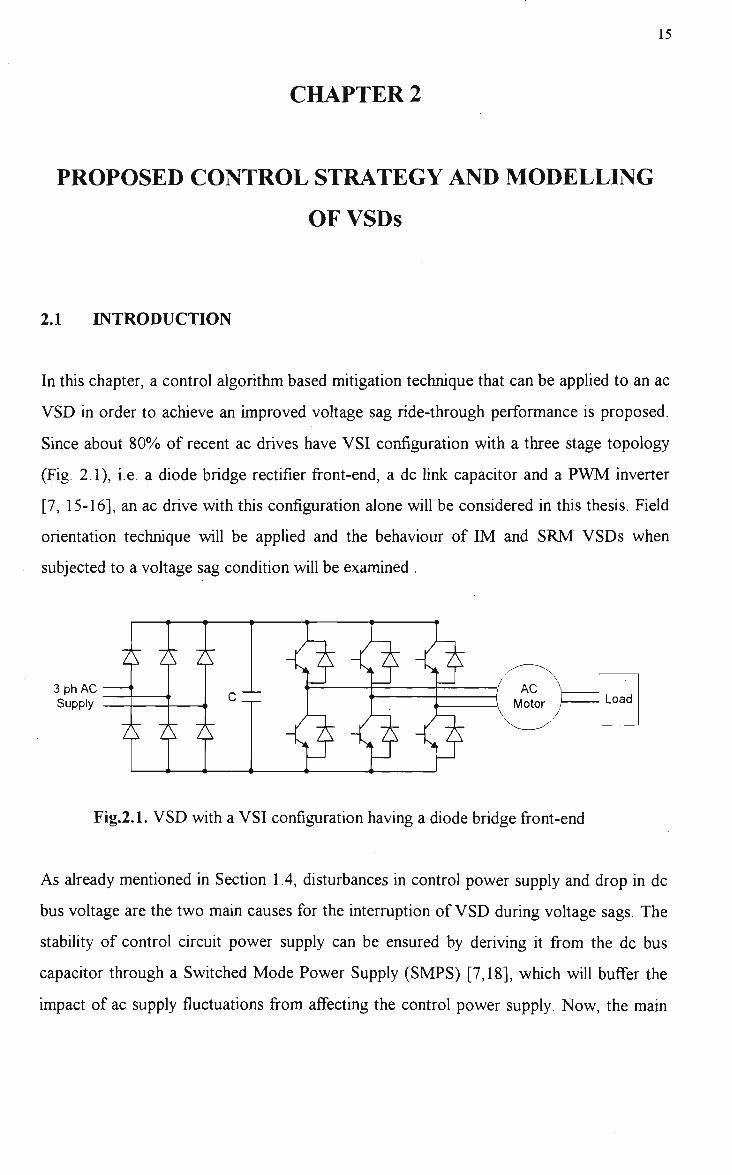
In this chapter, a control algorithm based mitigation technique that can be applied to an ac
V S D in order to achieve an improved voltage sag ride-through performance is proposed.
Since about 8 0 % of recent ac drives have VSI configuration with a three stage topology
(Fig. 2.1), i.e. a diode bridge rectifier front-end, a dc link capacitor and a P W M inverter
[7, 15-16], an ac drive with this configuration alone will be considered in this thesis. Field
orientation technique will be applied and the behaviour of I M and S R M V S D s when
subjected to a voltage sag condition will be examined .
3phAC Supply
Fig.2.1. V S D with a VSI configuration having a diode bridge front-end
As already mentioned in Section 1.4, disturbances in control power supply and drop in dc
bus voltage are the two main causes for the interruption of V S D during voltage sags. The
stability of control circuit power supply can be ensured by deriving it from the dc bus
capacitor through a Switched M o d e Power Supply (SMPS) [7,18], which will buffer the
impact of ac supply fluctuations from affecting the control power supply. N o w , the main

Strategy
task of the V S D control system is to maintain the dc bus voltage at a desired level during a
voltage sag so that the drive rides-through the sag without tripping due to the fault
conditions which were discussed in Section 1.4.
As shown in Appendix A, during normal operating conditions, there is a considerable
amount of energy present in an ac motor in the form of kinetic energy due to system
inertia and magnetising energy in the motor winding inductances. W h e n a voltage sag
occurs, the dc bus voltage can be maintained at a desired level by coordinated recovery of
energy from these two sources so that the continuity of operation of the V S D can be
achieved.
In this chapter, the proposed control strategy will be discussed in further detail. Because
this strategy requires modifications in the V S D control algorithm, there will be a brief
mention about the basic control loops used in a V S D operating under field orientation
which will be followed by a simplified block diagram representation of the Evl and S R M
V S D s for simulation purposes. Then, the design details of the additional control loops
required by this strategy and their operation sequence in coordination with the existing
control loops will be elaborated. Since there is a continuous flow of energy between the ac
mains, dc bus capacitor and the ac motor, and moreover because the proposed control
strategy aims to recover energy from the motor to the dc capacitor during a voltage sag,
the power flow equations involving the ac mains, V S D and the ac motor will be presented.
2.2 PROPOSED CONTROL STRATEGY
Out of the two sources of energy within the ac motor, viz. kinetic energy (\ Jco1) and the
magnetising energy (\LI2), the kinetic energy is the most dominant component and at
rated motor speed, it usually accounts for several times the energy stored in the capacitor
(refer Appendix A). The kinetic energy can be recovered from the rotating mass by
operating the P W M inverter in the regeneration mode i.e. by operating the motor as a

Chapter 2: Proposed Control Strategy and Modelling of VSDs 17
generator and by reversing the flow of energy from the motor to the dc bus. The
magnetising energy stored in the motor inductance can be recovered by forcing the
magnetising current reference to a lower value when the inductance acts as a current
source and feeds the stored energy back to the dc bus. The energy thus recovered in both
cases can be utilised to maintain the dc bus voltage at a desired level during a sag
In order to establish an efficient and simpler control system, it is better to attempt energy
recovery from one source at a time. The fact that the motor requires magnetic field in
order to function as a generator makes kinetic energy the first choice of energy source that
can be recovered. W h e n the motor functions as a generator, its speed falls more rapidly
than normal coasting, i.e. with the incoming supply cut off. The rate of speed drop during
regeneration depends on factors such as the amount of energy regenerated, the load torque
and system inertia. W h e n the motor speed reaches very low values, the stored kinetic
energy reaches negligible proportions and the motor cannot deliver the power required at
the dc bus. There is no advantage in reducing the speed below some limit. Hence, a cut-off
speed limit is defined below which, this strategy would attempt to recover the energy
available in the magnetising inductances.
2.2.1 SET POINTS FOR CONTROL STRATEGY
Under normal circumstances, a voltage sag condition can be detected by the VSD control
system by monitoring either the line-to-line ac supply voltage (Vu) or the dc capacitor
voltage (Vbus). Since the proposed control strategy is aimed at maintaining the dc bus
voltage at a desired value during a sag, a voltage sag should be detected in this case by
monitoring the incoming three-phase supply voltage only. Since as per the definition, a
voltage sag is reduction in rms supply voltage between 0.1 to 0.9 p.u. of the nominal value
[5,10], whenever any of the three line-to-line supply voltages to the V S D drop below 9 0 %
of the nominal ac voltage, a sag condition is declared and remedial actions are taken.

Chapter 2: Proposed Control Strategy and Modelling of VSDs 18
The set point for the bus voltage (Vbusred during a voltage sag is also very important for
proper coordination of the V S D under the proposed strategy. In the case of a three phase
rectifier, the,dc bus voltage (Vbus) is normally 1.35 times the rms line-to-line voltage (Vu).
W h e n a voltage sag occurs, the dc bus voltage falls below the nominal level. The deeper
the sag magnitude becomes, the lower the dc bus voltage will be and the higher will be the
chances of the V S D tripping due to under-voltage or over-current faults (as already
explained in section 1.4). Usually in a V S D , the under-voltage trip settings are user
configurable and are kept as a percentage of the nominal voltage (typically between 7 0 %
and 8 5 % ) [19]. Ideally, the bus voltage should be maintained between the nominal voltage
and trip setting when a sag occurs. Here, the bus voltage reference is kept as 1 0 0 % of the
nominal rated dc bus voltage for reasons that will be explained during the ride-through
simulations in Chapters 3 and 4.
Earlier in this section, a cut-off speed for the control transition in the energy recovery from
kinetic energy to magnetising energy was mentioned. Though theoretically the motor can
be operated in regeneration mode down to zero speed, in this simulation the cut off point
is kept at 1 0 % of the rated speed because less than about 1 % of the rated kinetic energy is
available in the motor below this speed.
2.2.2 CONTROL SEQUENCE AND FLOW CHARTING
The sequential flowchart of the VSD control during a voltage sag condition is as shown in
Figure 2.2.
It can be observed from the flowchart that, as per the proposed control strategy, there are
three distinct situations involved with respect to the control of the V S D . They are
summarised as follows.
Control Situation 1 (CS1): (No Voltage sag) VSD operation with normal speed control.
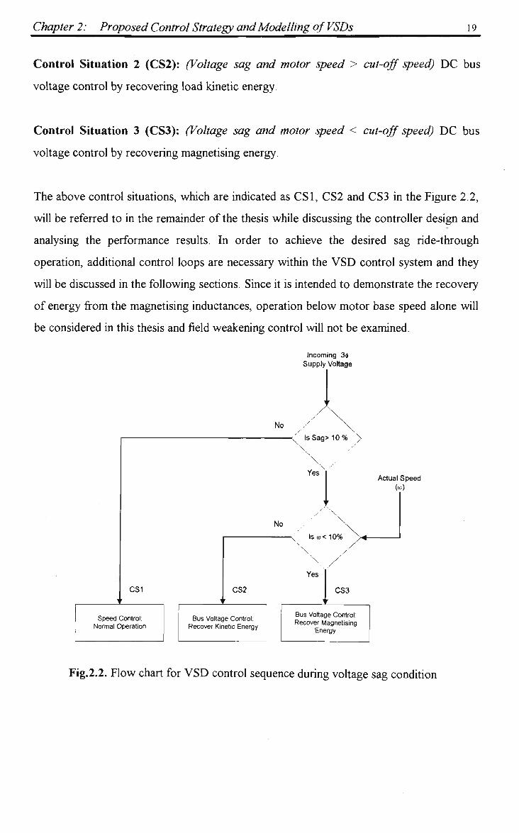
Chapter 2: Proposed Control Strategy and Modelling of VSDs 19
Control Situation 2 (CS2): (Voltage sag and motor speed > cut-off speed) D C bus
voltage control by recovering load kinetic energy.
Control Situation 3 (CS3): (Voltage sag and motor speed < cut-off speed) DC bus
voltage control by recovering magnetising energy.
The above control situations, which are indicated as CS1, CS2 and CS3 in the Figure 2.2,
will be referred to in the remainder of the thesis while discussing the controller design and
analysing the performance results. In order to achieve the desired sag ride-through
operation, additional control loops are necessary within the VSD control system and they
will be discussed in the following sections. Since it is intended to demonstrate the recovery
of energy from the magnetising inductances, operation below motor base speed alone will
be considered in this thesis and field weakening control will not be examined.
Incoming 34 Supply Voltage
No
No
CS1
Actual Speed (»)
Yes
CS2
Speed Control: Normal Operation
Bus Voltage Control Recover Kinetic Energy
CS3
Bus Voltage Control: Recover Magnetising
Energy
Fig.2.2. Flow chart for V S D control sequence during voltage sag condition
Chapter 2: Proposed Control Strategy and Modelling of VSDs 20
2.3 CONTROL LOOPS IN AC VSDs OPERATING UNDER FIELD
ORIENTATION
In this section, an overview of the basic control loops in an ac VSD will be presented and
the control block diagrams of I M and S R M V S D s will be discussed. In field oriented
control of ac motors, the three phase motor currents are transformed into two orthogonal
components in a synchronous frame of reference which moves with respect to the stator
axes, and they are defined as isq, the torque producing component and iS(j, the flux
producing component [26]. The mathematical relationships between these current vectors
for I M and S R M are shown in Appendices B and C respectively. A brief overview of the
control loops used in ac V S D s is as follows:
For the speed control of an ac motor, two sets of control loops are used in the VSD, viz.
(a) a speed controller working in conjunction with a current controller for the torque
producing current component (isq) and (b) a flux controller working in conjunction with
another current controller for the flux producing current component (/'**) [27]. Usually all
these controllers are of proportional-integral (PI) control type operating in closed loop
configuration.
The main purpose of the speed controller is to regulate the motor speed at a set reference.
The speed regulator generates the torque reference to the motor depending on the
instantaneous speed error and the controller gain values. In closed loop speed control, the
torque reference tends to control the motor to reach the set speed by minimising the speed
error to zero. In order to protect the motor from being subjected to excessive currents, the
speed regulator output is limited by a torque limiter. The limited torque reference is
converted to torque producing current reference (isqrej) which forms the control input to
the torque producing current regulator. This current regulator functions in a similar
manner to the speed regulator but generates set points for motor terminal voltage so that,
in closed loop control, the motor continues to run at the set speed for load torque
variations between zero and the torque limit. W h e n the load torque demand exceeds the
Chapter 2: Proposed Control Strategy and Modelling of VSDs 21
torque limit, the actual motor torque is clamped at this limit and the motor speed drops
below the set reference.
The flux controller regulates the actual flux (or magnetising current) to the set value and it
produces the flux producing current reference (iSdreJ)- The corresponding current regulator
controls the flux producing current component by again influencing the set points for
motor terminal voltage.
Finally, the output of the above control loops, i.e. the voltage set points, decide the
switching vector selection as required by the P W M inverter at any instant. Based on the
selected vector, the switches in the three inverter legs (Fig.2.1) are either opened or
closed, thereby connecting the motor terminals to either the positive or negative dc bus
and thus the voltage applied to the motor is controlled by the V S D control system.
The functional block diagram representation of VSD control scheme for IM and SRM
V S D s operating under field orientation is discussed in the following subsections.
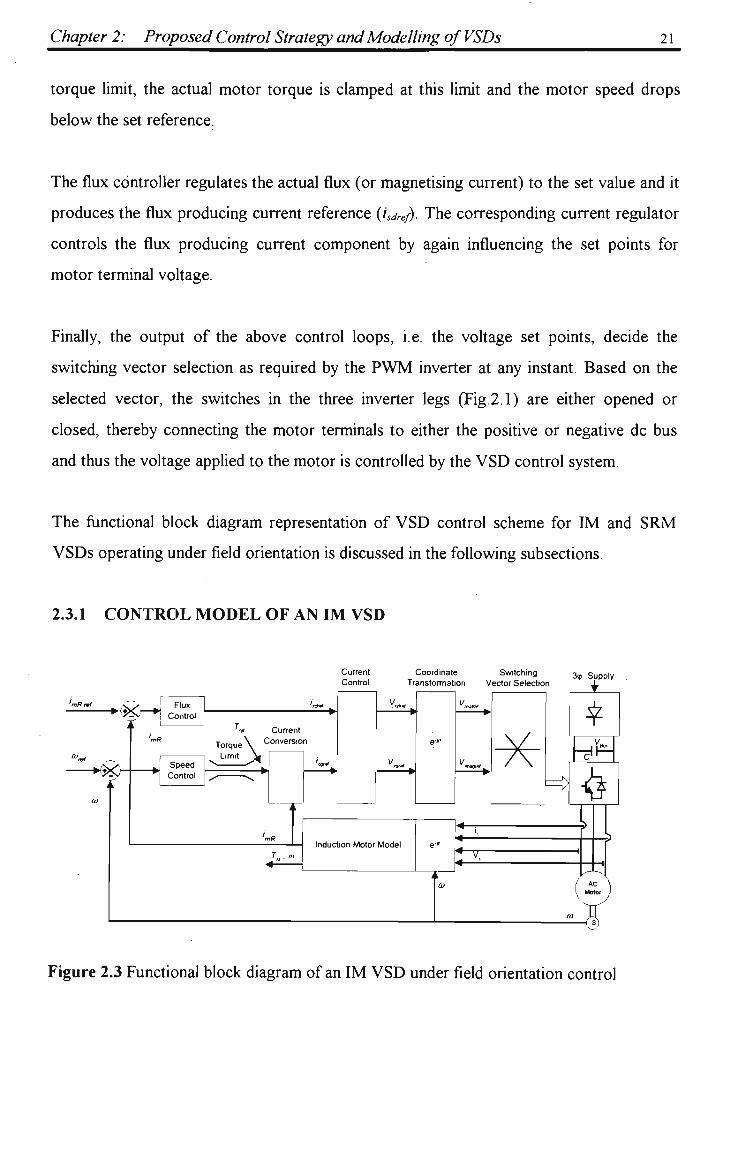
2.3.1 CONTROL MODEL OF AN IM VSD
Current Coordinate Switching 3. Supply Control Transformation Vector Selection X
Figure 2.3 Functional block diagram of an I M V S D under field orientation control

Chapter 2: Proposed Control Strategy and Modelling of VSDs 22
Figure 2.3 shows the simplified block diagram representation of an IM VSD operating
under field orientation, which is based on the motor modelling described in Appendix B.
Tuning details of the controllers are discussed in Appendix E.
For speed control of an induction motor, the speed reference (ah-ej) and the magnetising
current reference (imRref) are the two main control inputs. The Flux Controller generates
the flux producing current reference (isdref) whereas the speed PI controller generates the
torque reference, which after being limited, is converted to the torque producing current
reference (isqref) in the Current Conversion block. Based on the current references (isdref
and iSqref), the Current Control block generates the voltage set points ( F ^ / a n d Vsqref). In
field oriented control of induction motors, the synchronous coordinates are displaced
from the stator coordinates by an angle p as explained in Appendix B. In order to select
the proper switching vector as required by the control system, it is necessary to transform
these voltage reference values into real and imaginary coordinates fixed to the stator
reference frame and this is done by the Coordinate Transformation block. Finally, the
required switching sequence of the inverter switches is selected by the Switching Vector
Selection block, the details of which are explained in Appendix D.
Based on the inverter switching sequence and the instantaneous dc bus voltage at the
rectifier output, a three-phase ac voltage is applied to the motor terminals. In actual case,
the flux and current controllers are of proportional-integral (PI) type and the motor speed
is sensed by the control system from the speed sensor feedback (or by means of indirect
speed estimation methods). Other motor variables such as voltages and currents in field
coordinates and motor torque are computed from the terminal voltages and currents by the
built-in motor model within the V S D as shown in the control block diagram (Figure 2.3).
However, in this simulation, the motor variables such as voltages (VSd and Vsq), currents
(isd and isq), torque (TM) and speed (co) are calculated based on the actual switching vector
selected and the instantaneous dc capacitor voltage (Vbus), utilising the I M equations
whose derivations are explained in Appendix B. The three-phase ac supply, diode bridge

Chapter 2: Proposed Control Strategy and Modelling of VSDs 23
rectifier and dc bus capacitor are also modelled in the V S D control system. The control
equations used in the various control blocks are summarised as follows:
The Flux Control block calculates the motor flux producing current reference (isdref) from
the magnetising current reference (imRref) utilising the following equation:
hd = imR+^TR (2.1)
where,
isd - stator d-axis current,
imR - rotor magnetising current,
TR - rotor time constant
The Torque / Current Conversion block utilises the following motor torque equation in
order to calculate the torque producing current set point (isqset) from the set torque
reference (Tref):
TM=NppKimRisq (2.2)
where,
2*L„ K = "m
3%l + or)
Npp - number of pole pairs in the motor,
imR - magnetising current reference,
Lm - mutual inductance between stator and rotor windings, and
or - rotor leakage factor.
The Current Control block calculates the stator voltage set points in field coordinates
(Vsdrefand Vsqref) based on the following equations:
Vsd = fyd + °L*^ ~ "mR jsq) + (1 " °)LS ^E- (2.3)
disq Vsq = Rshq + °Ls i-^~ + <»mR lsd ) + 0 ~ CT)LS COmR imR (2.4)
Chapter 2: Proposed Control Strategy and Modelling of VSDs 24
where,
Rs - stator resistance,
Ls - stator inductance,
o - total leakage factor,
O)„,R - angular velocity of the magnetising vector
The Coordinate Transformation block transforms the selected voltage references (Vsdref
and Vsqref) from the synchronous coordinates to the stator coordinates according to
equation (2.5):
V* = Vs_real + JVsJmag = (Vsd + jVsq )eiP (2.5)
where,
p - angle between the synchronous and stator coordinates.
Vs - stator voltage vector
The Switching Vector Selection block selects the appropriate operating sequence for the
inverter switches, based on Vreairef and Vimagref chosen in the Coordinate Transformation
block. The details of vector selection are explained in Appendix D.
The Induction Motor Model calculates the actual motor voltages, currents (in d-q axes)
and torque depending on the switching vector selected and the instantaneous capacitor
voltage (Vbus) utilising equations (2.1) to (2.5). The motor speed is calculated by
integrating equation (2.6).
dco =V M L) (2.6) *J
where
TM - motor torque,
TL - load torque, and
J- system inertia.

Chapter 2: Proposed Control Strategy and Modelling of VSDs 25
2.3.2 CONTROL MODEL OF AN SRM VSD
Current Coordinate Switching 39 Supply Control Transformation Vector Selection 1
Fig 2.4 Functional block diagram of an S R M V S D under field orientation control
The simplified control block diagram of an SRM VSD under field orientation control is
represented in Figure 2.4. The motor modelling and the tuning of the controllers are
explained in Appendices C and F respectively.
In the case of an S R M V S D , velocity reference (cc^ef) and magnetising current reference
(isdref) form the control inputs. The main difference in the control of S R M s as compared to
the induction motors is due to the orientation of the flux axis. In the case of an S R M , the
flux axis aligns itself with the rotor axis and the magnetising current is the direct
component of the stator current vector (i$d)- The details of the current vectors and their
angular relationships in the various coordinates are explained in Appendix C for an S R M .
The control of an S R M is similar to that of an I M with similar control blocks as explained
in Subsection 2.3.1. The following S R M equations are used in the various control blocks:
3
2 TM ~ TNppi^sd ~^sq^sdhq
dco TM~TL=J- dt
(2.7)
(2.8)

Chapter 2: Proposed Control Strategy and Modelling of VSDs 26
vsd = Rsisd + Lsd-^-o) Lsqisq (2.9)
diSq Vsq = Rshq +Lsq — + a) Lsdisd (2.10)
Vs = Vs_real + JVs_imag = (Vsd + JVSq)e
j£ (2.11)
where,
TM- motor torque
TL- load torque
J- system inertia
Npp - number of pole pairs
Rs - stator resistance
Lsd, Lsq - stator inductance in d and q axes
e - rotor angle with respect to stator axis
co - rotor angular velocity
Vs- stator voltage vector
hd, isq - stator currents in d and q axes
Vsd, Vsq - stator voltages in d and q axes
2.4 PROPOSED ADDITIONAL CONTROL LOOPS FOR DC BUS VOLTAGE
CONTROL
It may be recalled from Section 2.2 that the main intent of the proposed control strategy is
to maintain the capacitor voltage at the nominal value by recovering the kinetic as well as
the magnetising energy available in the motor. Three control situations were defined, viz.
(a) N o sag situation (Control Situation 1), (b) A voltage sag condition with the motor
running above the cut-off speed limit (Control Situation 2) and (c) A voltage sag condition
with the motor running below the cut-off speed limit (Control Situation 3). A n overview
of the basic control loops for the speed control of I M and S R M V S D s was presented in
Section 2.3. From the point of view of the proposed control strategy, these are the control
Chapter 2: Proposed Control Strategy and Modelling of VSDs 27
loops that will be in operation during a no sag situation (Control Situation 1). However,
since there is a need to recover the energy present in the motor during a sag, additional
control loops are necessary in the V S D control system. The control methodology, design
and implementation of the additional control loops will be discussed in the following
subsections and their sequence of operation in coordination with the existing control loops
will be defined. Tuning details of the additional controllers are presented in Appendices E
and F for I M and S R M respectively.
2.4.1 BUS VOLTAGE CONTROL BY RECOVERING LOAD KINETIC
ENERGY
At higher motor speeds, the capacitor voltage can be controlled by recovering the kinetic
energy available in the rotating mass. Kinetic energy can be recovered by operating the
motor as a generator. Electrically this means reversal of the flow of current from the ac
motor to the dc bus with rated flux applied to the motor. From a control point of view,
this can be achieved by maintaining the flux reference to the motor constant at the rated
value and by reversing the polarity of the torque reference (Trej) which, in turn, will reverse
the flow of isq. This operation is further explained by the power balance equation (2.12)
whose derivation will be shown in Section 2.5.
2
Vbus lout — — ft'sdlsd + Vsq Isq) (2-12)
where,
Vbus - bus capacitor voltage
lout - dc current flowing between the bus capacitor and the inverter
Vsd, VSq- stator voltages in synchronous coordinates
isd, isq - stator currents in synchronous coordinates
From equation (2.12), it can be noted that, by maintaining the flux (isd) constant, if isq is
reversed, the flow of the dc current /„„, can be reversed from the motor to -the dc bus
Chapter 2: Proposed Control Strategy and Modelling of VSDs 28
which will boost the capacitor voltage. This is the basis of the control utilised in Control
Situation 2.
In a voltage sag condition, the recovery of kinetic energy must be controlled so that only
the required amount of energy is recovered from the motor to maintain the capacitor
voltage at the desired value. This can be done by the use of a closed loop proportional-
integral (PI) controller, which monitors the capacitor voltage against the set reference and
produces a suitable torque reference. The polarity of the torque reference is reversed to
that of normal speed control operation. A new PI controller is configured in the V S D
control system for this purpose which will be referred to as Bus Voltage Controller 1 in
further discussions.
As described in Section 2.3, during normal speed control operation (Control Situation 1),
the torque reference is generated by the Speed Controller in order to regulate the motor
speed at the set reference. W h e n a sag occurs, if the motor speed is above the cut-off limit
(i.e. Control Situation 2), the torque control is switched to the Bus Voltage Controller 1.
This controller applies a reverse torque reference and controls the capacitor voltage rather
than motor speed. The Current Controller as well as rest of the control blocks (which are
shown in Figures 2.3 and 2.4) operate exactly in the same manner as during speed control
and motor speed is not controlled in this situation. Because of the regenerative operation,
the motor speed will reduce rapidly during this control. While recovering the kinetic
energy, the torque limiting circuit must be in circuit to ensure that the motor currents are
within the allowable levels. The transition between the Speed Controller and Bus Voltage
Controller 1 is reversible when the motor speed is above the cut-off limit, i.e. when a sag
occurs, torque referencing switches from Speed Controller to Bus Voltage Controller 1
and vice versa if the sag disappears when the motor speed is still above the cut-off limit.
The magnetising current reference is maintained at the rated value throughout this
operation. Figure 2.5 shows the sequence of operation of the control system during a sag
at high motor speeds. Control Situations 1 and 2 are indicated as CS1 and C S 2
respectively.

Chapter 2: Proposed Control Strategy and Modelling of VSDs 29
"ret Speed
Controller
CS1 — ^ v
Current Conversion
>> y y^~
' ref
Bus Voltage Controller 1
CS2 y ->*'
Torque Limit
sqret
CS1
Rated magnetising current reference > ^
cs2 y -•o'
Current Limit
Figure 2.5 Control loop to recover kinetic energy
Since the basis of speed and torque control operation is identical for IM and SRM VSDs,
as explained in Section 2.3, the proposed control scheme is applicable for both motor
types. The control strategy at motor speeds lower than the cut-off speed limit is discussed
in the following subsection.
2.4.2 BUS VOLTAGE CONTROL BY RECOVERING MAGNETISING
ENERGY
If a voltage sag occurs when the motor speed is below the cut-off limit (Control Situation
3), the magnetising energy stored in the motor inductance can be recovered to boost the
bus capacitor voltage. This energy recovery can be achieved by lowering the magnetising
current, (which is /«/ for an S R M and i„n for an IM). From the stator voltage equations,
(equations (2.3) and (2.9) respectively in the case of I M and S R M ) , it can be found that
lowering the magnetising current reference results in the polarity reversal of the applied
voltage V,d. There is no torque needed during this control situation and hence isq is
controlled to zero. From the power flow equation (2.12), which was referred to in
Subsection 2.4.1, it can be noted that, with zero isq, reversal of Vsd reverses the flow of the
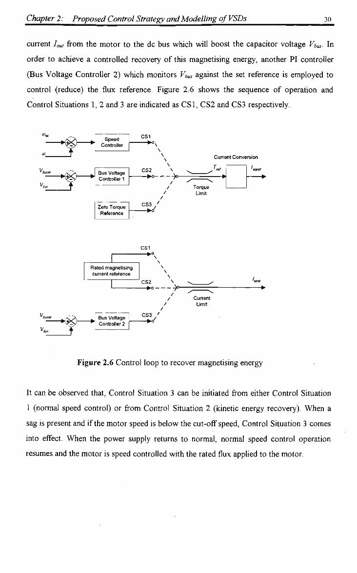
Chapter 2: Proposed Control Strategy and Modelling of VSDs 30
current Iout from the motor to the dc bus which will boost the capacitor voltage V^. In
order to achieve a controlled recovery of this magnetising energy, another PI controller
(Bus Voltage Controller 2) which monitors V^ against the set reference is employed to
control (reduce) the flux reference. Figure 2.6 shows the sequence of operation and
Control Situations 1, 2 and 3 are indicated as CS1, CS2 and CS3 respectively.
Speed Controller
-H&H-* Bus Voltage Controller 1
Zero Torque Reference
CS1
CS2 V — • o -)o-
/ /
/ /
CS3 / ->o
Current Conversion
y^ Torque Limit
'sqref
Rated magnetising current reference
Bus Voltage Controller 2
CS1
•°(.
CS2 ^ —•<> -)o-
/ /
/ /
CS3 / •o/
Current Limit
Figure 2.6 Control loop to recover magnetising energy
It can be observed that, Control Situation 3 can be initiated from either Control Situation
1 (normal speed control) or from Control Situation 2 (kinetic energy recovery). When a
sag is present and if the motor speed is below the cut-off speed, Control Situation 3 comes
into effect. When the power supply returns to normal, normal speed control operation
resumes and the motor is speed controlled with the rated flux applied to the motor.

Chapter 2: Proposed Control Strategy and Modelling of VSDs 31
2.5 POWER BALANCE BETWEEN AC SUPPLY, BUS CAPACITOR AND AC
MOTOR
Between AC Supply and Bus Capacitor Between Bus Capacitor and AC Motor
Diode VSI Rectifier Inverter
Fig. 2.7 Power flow diagram in an ac V S D
Since the proposed control strategy aims to recover energy from the motor to the dc
capacitor during a voltage sag and also because there is a continuous flow of energy
between the ac mains, dc link and the ac motor, the power flow equations relating the
voltages and currents in these sources are discussed here. The V S D configuration
considered in this thesis is shown in Figure 2.1. During motoring, power flows from the
incoming ac supply to the dc bus capacitor (through the diode bridge rectifier) and from
the bus capacitor to the motor (through the P W M inverter). W h e n the motor is controlled
in regeneration mode, the inverter reverses the direction of power flow from the motor to
the dc capacitor. Figure 2.7 shows the power flow block diagram of the V S D
configuration considered in this thesis. The currents and voltages in the ac motor are
represented in synchronous coordinates. The derivation of power balance equations
between ac-to-dc and dc-to-ac conversions are discussed in the following subsections.
2.5.1 POWER FLOW BETWEEN AC SUPPLY AND DC BUS CAPACITOR
In a diode-bridge rectifier, when the line-to-line ac voltage (Vij) is greater than the
instantaneous capacitor voltage (V^), there will be a flow of current (//) from the
conducting phases to the bus capacitor based on equation (2.13).
Chapter 2: Proposed Control Strategy and Modelling of VSDs 32
2L^ = Vll-2RIl-Vbus (2.13)
where,
L - per phase line inductance
R - per phase line resistance
Under balanced supply conditions with a constant load, the individual phase currents will
be a repetitive pattern of two symmetrical pulses in the positive as well as the negative half
cycles. Hence, the capacitor charging current (/,„) will be a uniform pattern of six pulses
per cycle. The instantaneous capacitor voltage (Vbus) can be calculated as:
„dVkUs C-%UL = Ii„-Iout (2.H)
The relationship between ac and dc quantities (i.e. voltages and currents) under balanced
three-phase supply conditions is,
//=0.816/l-„ (2.15)
Vbus = U5Vtt (2.16)
where,
// - incoming phase current,
Iin - capacitor charging current,
Vbus - capacitor voltage,
Vn - line-to-line ac voltage
2.5.2 POWER FLOW BETWEEN DC BUS CAPACITOR AND AC MOTOR
The relationships between the instantaneous power drawn from the bus capacitor and the
power utilised by the ac motor is derived in this subsection. The angular relationships of
current vectors in various reference frames are shown in Figure 2.8, which are explained in
further detail in Appendices B and C for both EV1 and SRM.

Chapter 2: Proposed Control Strategy and Modelling of VSDs 33
co «. . Rotor axis
mmR •% - Ma9ne,isin9 . T"" axis
Stator axis
0) w _ Rotor axis _, - -nT" (Magnetising
axis)
Stator axis
(a) For Induction Motor (b) For S R M
Figure 2.8 Angular relationships between current vectors in steady state [26]
The stator voltage and current vectors (VS,IS) can be expressed in terms of their three
phase components as follows:
Vs=Vsl+Vs2eJ* +Vs3e
J*
2K
J \n
where,
Vsi, Vs2, VS3 - individual phase voltages applied to the ac motor
Li, 1,2, Is3 - individual phase currents in the ac motor
(2.17)
(2.18)
In a star connected system, Isl + IS2 +Iss = 0 and hence, the instantaneous power/? flowing
into the ac motor can be derived as:
/7 = |Re(F,7/) (2.19)
Also, these stator voltage and current vectors (Vsandls) can be expressed in field
coordinates. In the case of an IM, p is the instantaneous angle of the rotating magnetising
axis with respect to the stationary frame of reference. (In the case of an S R M , this angle is
e, which is the angle of the rotor with respect to the stator axis. However the following
result still holds good for both motors).
Vse-JP = Vsd+jVs, sq
(2.20)
Chapter 2: Proposed Control Strategy and Modelling of VSDs 34
h e~JP = hd + Jhq (2-21)
Vs e~JP I* ejp = Vs I* = (Vsdhd + Vsqisq) +j (VsqiSd - Vsdisq) (2.22)
Substituting equation (2.22) into (equation (2.19),
p = |Re(F, I*) = (Vsd isd + Vsq isq) (2.23)
From Figure 2.7, it can be seen that the input power/? flowing into the motor from the
capacitor (neglecting losses) is:
p= V^, Io* (2.24)
Combining equations (2.23) and (2.24), the power balance between the dc bus and ac
motor is obtained as:
2 Vbus lout = - (Vsdisd + Vsq isq) (2.25)
2.6 SUMMARY
In this chapter, the basis and details of the proposed control strategy were described. In
order to enable sag ride-through of an ac motor V S D (with a VSI configuration), it is
suggested to maintain the dc bus voltage at the nominal (rated) value by recovering the
kinetic and magnetisation energy available in the motor. Operation of the basic control
loops used for speed and current control of IM and S R M V S D s were discussed. In order
to achieve the capacitor voltage control by recovering energy from the two sources, two
additional control loops were proposed and their coordination with the existing controllers
in the V S D was explained. The mathematical equations for power flow between the ac
mains, dc bus capacitor and the ac motor controlled by field orientation technique were
presented. As seen from the control structure of both I M and S R M , the proposed strategy
is applicable to both the motor types. In the forthcoming chapters the simulation results of
S R M and I M V S D s when controlled by this strategy will be analysed.
35
CHAPTER 3
PERFORMANCE OF A SYNCHRONOUS RELUCTANCE
MOTOR DRIVE
3.1 INTRODUCTION
In this chapter, the voltage sag ride-through performance of a synchronous reluctance
motor variable speed drive ( S R M V S D ) under the proposed control strategy is presented.
The details on the field orientation of an S R M can be found in Appendix C. The control of
an S R M , as illustrated in Subsection 2.3.2, is modelled in M A T L A B ™ .
Initially, there will be a brief mention on the type of voltage sags that will be applied in this
simulation. Then, the performance results of the S R M V S D during normal ac supply
conditions as well as during a sag will be presented. From these results, the reasons for
nuisance tripping of the V S D during a voltage sag will be discussed. Finally, the voltage
sag ride-through performance of the S R M V S D utilising the proposed control strategy will
be verified. It may be recalled that, as per the strategy defined in Section 2.2, the bus
voltage will be maintained at the nominal value during a sag by recovering the kinetic
energy available in the rotating mass when motor speed is above the cut-off limit (which is
1 0 % of the motor base speed), or by recovering the magnetising energy available in the
motor winding inductances below the cut-off speed limit. Because energy is recovered
from two sources under different conditions, the simulation results will be presented in
three parts, viz. (a) operation above the cut-off speed by recovering kinetic energy, (b)
operation below the cut-off speed by recovering magnetising energy and (c) coordinated
sag ride-through at all speeds by recovering from both sources of energy.
Chapter 3: Performance of a Synchronous Reluctance Motor Drive 36
Since kinetic energy is proportional to the square of the motor speed, it can supply the dc
bus for a longer duration and thus provide a longer sag ride-through operation if the rate
of speed drop is low. The speed drop of the motor during kinetic energy recovery depends
on two factors, viz. (a) amount of energy regenerated and (b) the load. The regenerated
energy is utilised to charge the dc bus capacitor as well as to compensate for the resistive
losses in the motor windings. The effect of reducing the bus capacitance will be studied on
the voltage sag ride-through behaviour of the S R M V S D later in this chapter. As far as the
effect of load is concerned, the sag ride-through duration will be maximum when the load
on the motor is a minimum. In this thesis, both constant torque and fan type loads are
considered. Fan type loads, in which the torque reduces with square of the motor speed
(TL oc co2), are expected to respond to this control strategy for much longer duration as
compared to constant torque loads. In this chapter, performance of the S R M V S D with a
constant torque load will be discussed whereas the performance results for a fan type load
will be discussed in Appendix I.
3.2 SAG TYPES UNDER STUDY
Section 1.3 presented four types of voltage sags, viz., Type A, B, C and D, which were
classified on the basis of whether they are single-phase or three-phase sags and whether
there are any phase shifts involved. One of the main reasons the effect of phase angle jump
is not critically analysed is because this parameter is not quantified and there are no
sensing equipment available to monitor phase jumps. The effect of phase angle jumps on
critical equipment is not well understood [7-8] and requires further investigation. In a
V S D with diode-bridge front-end, a phase shift tends to lead to a single-phasing situation
[7], In this thesis, the effect of phase shifts in the incoming supply is not studied.
Of the remaining two types of sags, viz. a three phase sag (Type A) and a single phase sag
(Type B), the three phase sag accounts for a large reduction in the dc bus voltage but does
not lead to a high dc voltage ripple. A single phase sag results in a reduction of two phase-
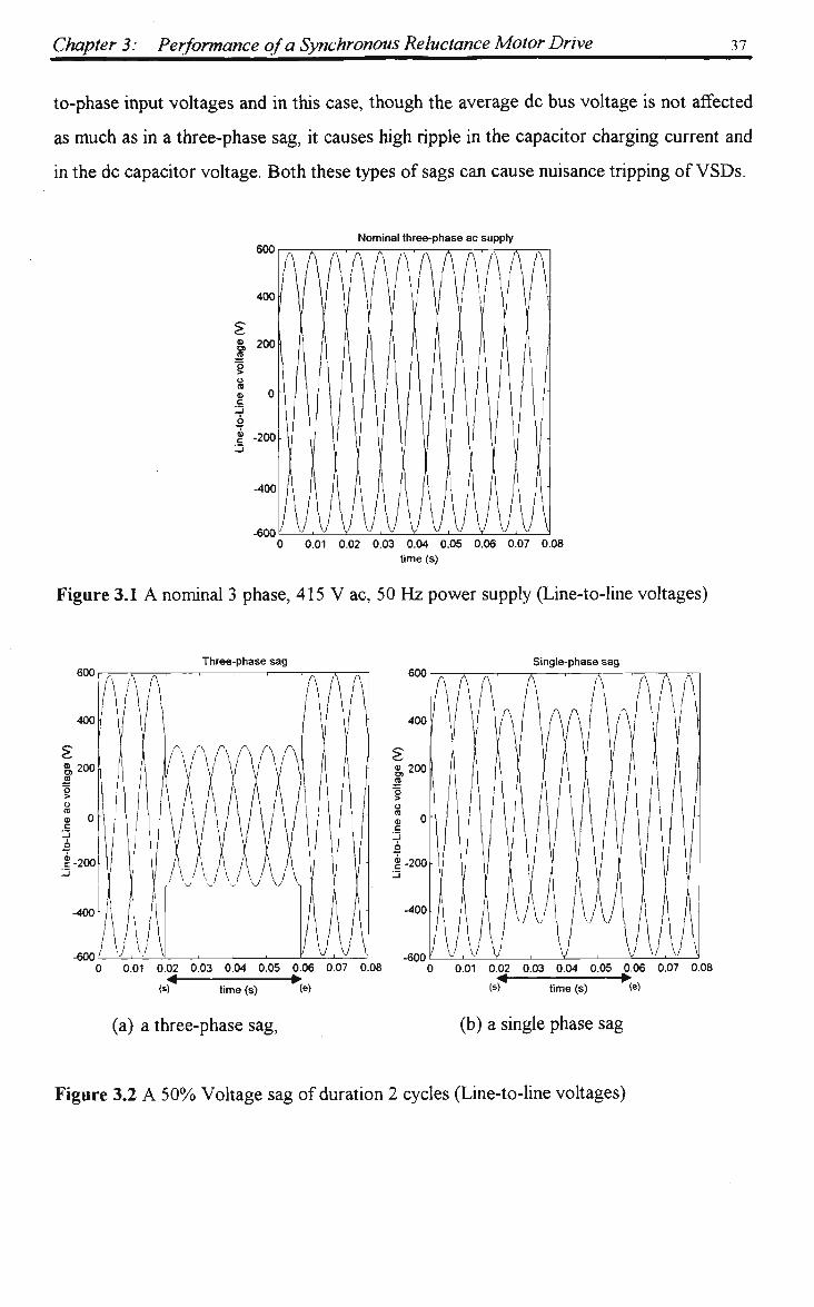
Chapter 3: Performance of a Synchronous Reluctance Motor Drive 37
to-phase input voltages and in this case, though the average dc bus voltage is not affected
as much as in a three-phase sag, it causes high ripple in the capacitor charging current and
in the dc capacitor voltage. Both these types of sags can cause nuisance tripping of VSDs.
600 Nominal three-phase ac supply
-600 0 0.01 0.02 0.03 0.04 0.05 0.06 0.07 0.08
time (s)
Figure 3.1 A nominal 3 phase, 415 V ac, 50 H z power supply (Line-to-line voltages)
600
400
8,200
Three-phase sag
•200
-400
-600
600 r Singte-phase sag
0 0.01 0.02 0.03 0.04 0.05 0.06 0.07 0.08
(s) time (s) (e)
(a) a three-phase sag,
600 t 0 0.01 0.02 0.03 0.04 0.05 0.06 0.07 0.08
(s) time (s) W
(b) a single phase sag
Figure 3.2 A 5 0 % Voltage sag of duration 2 cycles (Line-to-line voltages)

Chapter 3: Performance of a Synchronous Reluctance Motor Drive 38
A nominal ac power supply of 3 phase, 415 V ac, 50 Hz is considered in the simulation
work. Figure 3.1 and Figure 3.2 show a nominal power supply condition and a 5 0 %
voltage sag of duration 2 cycles (both three-phase and single-phase) respectively. The sag
condition is indicated by a double-sided arrow in Figure 3.2 with the start and end of the
sag indicated as (s) and (e) respectively.
As reported in [4], VSDs are likely to trip when subjected to a voltage sag of magnitude
greater than 2 0 % and duration more than 12 cycles. In this thesis, the behaviour of V S D s
when subjected to both single-phase and three-phase sags of magnitude 5 0 % and duration
50 cycles (1 second) will be studied. From the simulation results shown later in this
chapter, it can be seen that the proposed control strategy provides identical sag ride-
through behaviour for both types of sags. Since a three-phase sag represents the worst
case situation, the performance of the proposed control strategy will be analysed by
applying a three phase sag.
3.3 NORMAL SPEED CONTROL OPERATION OF AN SRM VSD
In this section, initially, the speed control behaviour of the SRM VSD will be verified
under normal ac supply conditions. Then, the behaviour of the V S D when subjected to a
voltage sag of both three-phase and single-phase types will be analysed. From the
simulation results, the reasons for V S D tripping on a sag will be discussed.
3.3.1 PERFORMANCE UNDER NORMAL OPERATING CONDITIONS - NO
SAG
Here, the response of an SRM VSD, under ideal power supply conditions (as shown in
Figure 3.1), is studied. This situation corresponds to Control Situation 1 as defined in the
control strategy (Subsection 2.2.2). The torque reference is controlled by the Speed

Chapter 3: Performance of a Synchronous Reluctance Motor Drive 39
Controller which aims to control the motor speed at the set reference. The SRM
parameters and V S D set points are listed in Appendix F and the details of Speed
Controller tuning are given in Appendix H. The S R M V S D was tested at various
operating conditions and the performance can be found to be satisfactory. The behaviour
of the S R M V S D during acceleration and at steady-state speed control is analysed in this
subsection.
Simulation conditions: The speed control simulation of the SRM VSD is carried out for
a duration of 1.75 seconds. A n inverter switching frequency of 5 k H z is considered. W h e n
a vector switching occurs, normally the transition takes place between the two inverter
switches in any one inverter leg, with one switch turning on and the other turning off (refer
Appendix D for details on switching sequence of the inverter switches during field
orientation control). Assuming that in one switching cycle, all the six switches complete a
full switching transition (i.e. on-to-off and off-to-on), a sampling frequency of 30 kHz is
chosen here so that the V S D response during every transition is gathered. The motor is
started from standstill and a speed reference of 120 rad/s is applied. The load torque (TL)
and the torque limit (TLT) are set at 5 0 % and 1 5 0 % of the rated motor torque (36 Nra)
respectively. The motor flux reference is set at the rated value (i.e. isdref = 9A). A system
inertia (J) of 0.23 kgm 2 is considered.
SRM VSD response: The SRM speed (co), torque (TM), magnetising current (/.«/) and
torque producing current (isq) during acceleration and steady-state speed control are
shown in Figure 3.3 (a) to (d) respectively. The dc bus characteristics, viz. the capacitor
output current (lout), the capacitor voltage (Vbus) and the capacitor charging current (/,„)
are shown in Figures 3.4(a) to (c) respectively. The transition from acceleration to steady-
state is indicated by a dotted vertical line (t).

Chapter 3: Performance of a Synchronous Reluctance Motor Drive 40
140 Motor speed (a>)
-S- 80
3 60
0 0.2 0.4 0.6 0.8 1 1.2 1.4 1.6 1.8 (t) time (s)
(a) Speed (co)
Stator d-axis current (i^
60
50
40
Motor Torque (J^
e z ,30
20
10
-
TL = 18 Nm
- r i • < - I
TLT = 54 Nm
-
.
.
-
0 0.2 0.4 0.6 0.8 1 1.2 1.4 1.6 1.8 (t) time (s)
35
30
25
20
15
10
(b) Torque (TM)
Stator q-axis current (i<q)
WWWWi^
\mmmmwm
(c) Magnetising current (isd)
0 0.2 0.4 0.6 0.8 1 1.2 1.4 1.6 1.8 (t) time (s)
(d) Torque producing current (isq)
Figure 3.3 S R M response during acceleration and steady-state speed control under ideal
ac supply conditions

Chapter 3: Performance of a Synchronous Reluctance Motor Drive 41
Capacitor output current (!„„,) 590
588
586
1584^
582
580
Capacitor voltage ( V ^
578 0.2 0.4 0.6 0.8 1 1.2 1.4 1.6 1.8
(t) time (s)
0 0.2 0.4 0.6 0.8 1 1.2 1.4 1.6 1.8 (t) time (s)
(a) Capacitor output current (7ouf) (b) Capacitor voltage (Vbus)
Capacitor charging current (!,„)
0 0.2 0.4 0.6 0.8 1 1.2 1.4 1.6 1.8 C time (s)
(c) Capacitor charging current (/,„)
Figure 3.4 S R M V S D dc bus characteristics during acceleration and steady-state speed
control under ideal ac supply conditions
As shown in Figures 3.3(a) and (b), the S R M is found to accelerate to the set speed under
torque limit. The observed acceleration time of about 0.75 seconds is found to coincide
with the duration calculated using equation (3.1). The motor flux (isd) is found to be
controlled at the rated value (Figure 3.3(c)) during both acceleration and steady-state.

Chapter 3: Performance of a Synchronous Reluctance Motor Drive 42
Because of this constant flux control, the torque producing current component isq is found
to follow the characteristics of the motor torque (TM) according to equation (3.2) as
observed in Figures 3.3 (b) and (d).
JAco 0.23*120 A„,, A/ = = = 0.766s
(TM-TL) (54-18)
*M ~ 2 PP ^sd'^sq) lsd hq
p = CO TM
where,
J- system inertia,
TM - motor torque
Ti - load torque
L^ -stator d-axis inductance
Lsq -stator q-axis inductance
Npp - number of pole pairs
p - power input to motor
co - motor speed
The dc bus characteristics (as shown in Figure 3.4) are found to be in accordance with the
motor characteristics throughout the operation. During acceleration, since the power
applied to the motor (p) increases according to equation (3.3), the dc output current to the
motor (1^) is found to increase in Figure 3.4(a). Hence, the dc voltage ripple and the
capacitor charging current are also found to increase during acceleration as observed in
Figures 3.4 (b) and (c) respectively.
Once the set speed is reached, the motor speed is found to be maintained at this value as
observed in Figure 3.3(a). The implementation of the integrator wind-up reset feature has
ensured that no overshoot has occurred in the motor speed during the transition from
acceleration to steady state, which otherwise might have occurred due to the saturation of
(3.1)
(3.2)
(3.3)
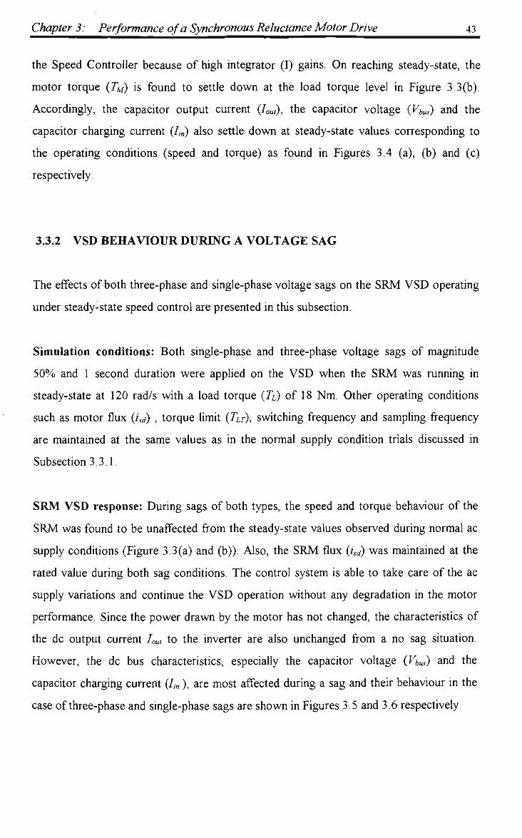
Chapter 3: Performance of a Synchronous Reluctance Motor Drive 43
the Speed Controller because of high integrator (I) gains. On reaching steady-state, the
motor torque (7^,) is found to settle down at the load torque level in Figure 3.3(b)
Accordingly, the capacitor output current (hut), the capacitor voltage (Vbus) and the
capacitor charging current (/,„) also settle down at steady-state values corresponding to
the operating conditions (speed and torque) as found in Figures 3.4 (a), (b) and (c)
respectively.
3.3.2 VSD BEHAVIOUR DURING A VOLTAGE SAG
The effects of both three-phase and single-phase voltage sags on the SRM VSD operating
under steady-state speed control are presented in this subsection.
Simulation conditions: Both single-phase and three-phase voltage sags of magnitude
5 0 % and 1 second duration were applied on the V S D when the S R M was running in
steady-state at 120 radVs with a load torque (TL) of 18 N m . Other operating conditions
such as motor flux (isd) , torque limit (TLT), switching frequency and sampling frequency
are maintained at the same values as in the normal supply condition trials discussed in
Subsection 3.3.1.
SRM VSD response: During sags of both types, the speed and torque behaviour of the
S R M was found to be unaffected from the steady-state values observed during normal ac
supply conditions (Figure 3.3(a) and (b)). Also, the S R M flux (iSd) was maintained at the
rated value during both sag conditions. The control system is able to take care of the ac
supply variations and continue the V S D operation without any degradation in the motor
performance. Since the power drawn by the motor has not changed, the characteristics of
the dc output current lout to the inverter are also unchanged from a no sag situation.
However, the dc bus characteristics, especially the capacitor voltage (Vbus) and the
capacitor charging current (//„), are most affected during a sag and their behaviour in the
case of three-phase and single-phase sags are shown in Figures 3.5 and 3.6 respectively.
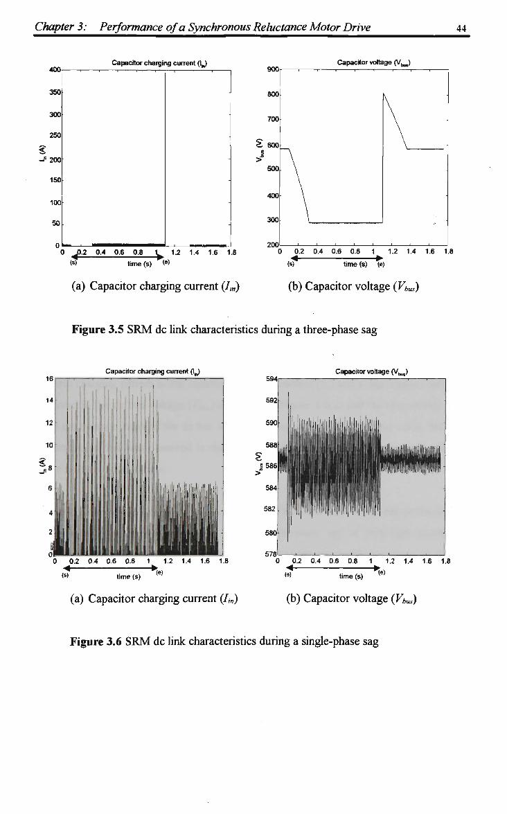
Chapter 3: Performance of a Synchronous Reluctance Motor Drive 44
400
350
300
250
§ --200
150
100
50
0
Capacitor charging current (IJ
•
.
•
•
900
800
700
600
500
400
300
•>nn
Capacitor voltage (V^J
,
\
\
0 J.2 0.4 0.6 0.8 1 1.2 1.4 1.6 1.8
(s) time (s) W
(a) Capacitor charging current (/*„)
0 0.2 0.4 0.6 0.8 1 1.2 1.4 1.6 1.8 ."!* " 7 7 — • (s) time (s) (e)
(b) Capacitor voltage (Vbus)
Figure 3.5 S R M dc link characteristics during a three-phase sag
Capacitor charging current (I*,)
(s) time (s)
(a) Capacitor charging current (/,„)
594 Capacitor voltage (V^J
592
590
588
l586|
584
582
580
578 0 0.2 0.4 0.6 0.8 1 1.2 1.4 1.6 1.8
< •?. (s) time (s) (e)
(b) Capacitor voltage (Vbus)
Figure 3.6 S R M dc link characteristics during a single-phase sag
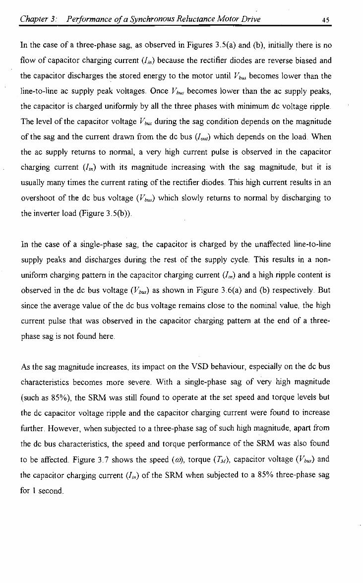
Chapter 3: Performance of a Synchronous Reluctance Motor Drive 45
In the case of a three-phase sag, as observed in Figures 3.5(a) and (b), initially there is no
flow of capacitor charging current (/,„) because the rectifier diodes are reverse biased and
the capacitor discharges the stored energy to the motor until Vbus becomes lower than the
line-to-line ac supply peak voltages. Once Vbus becomes lower than the ac supply peaks,
the capacitor is charged uniformly by all the three phases with minimum dc voltage ripple.
The level of the capacitor voltage Vbus during the sag condition depends on the magnitude
of the sag and the current drawn from the dc bus (lout) which depends on the load. W h e n
the ac supply returns to normal, a very high current pulse is observed in the capacitor
charging current (Iin) with its magnitude increasing with the sag magnitude, but it is
usually many times the current rating of the rectifier diodes. This high current results in an
overshoot of the dc bus voltage (Vbus) which slowly returns to normal by discharging to
the inverter load (Figure 3.5(b)).
In the case of a single-phase sag, the capacitor is charged by the unaffected line-to-line
supply peaks and discharges during the rest of the supply cycle. This results in a non
uniform charging pattern in the capacitor charging current (/,-„) and a high ripple content is
observed in the dc bus voltage (Vbus) as shown in Figure 3.6(a) and (b) respectively. But
since the average value of the dc bus voltage remains close to the nominal value, the high
current pulse that was observed in the capacitor charging pattern at the end of a three-
phase sag is not found here.
As the sag magnitude increases, its impact on the VSD behaviour, especially on the dc bus
characteristics becomes more severe. With a single-phase sag of very high magnitude
(such as 8 5 % ) , the S R M was still found to operate at the set speed and torque levels but
the dc capacitor voltage ripple and the capacitor charging current were found to increase
further. However, when subjected to a three-phase sag of such high magnitude, apart from
the dc bus characteristics, the speed and torque performance of the S R M was also found
to be affected. Figure 3.7 shows the speed (co), torque (TM), capacitor voltage (VbUs) and
the capacitor charging current (/,„) of the S R M when subjected to a 8 5 % three-phase sag
for 1 second.
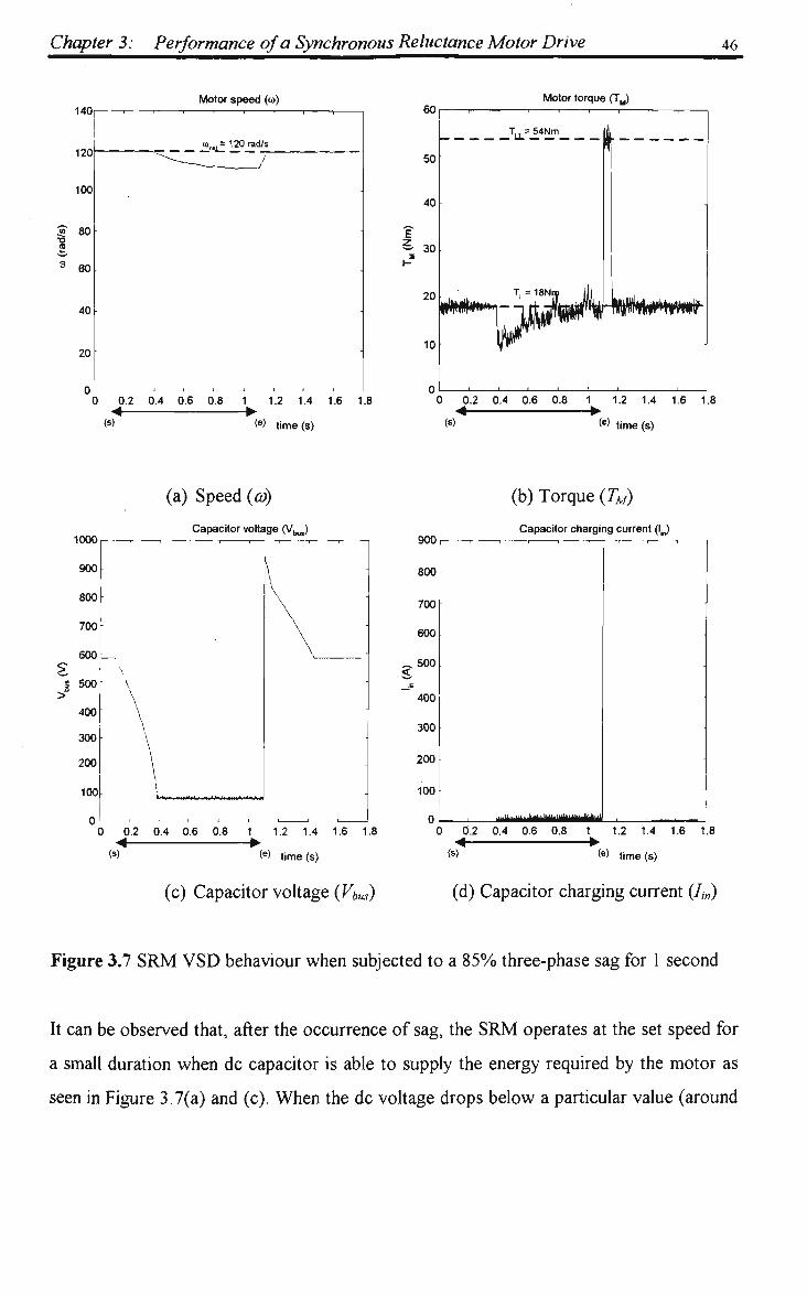
Chapter 3: Performance of a Synchronous Reluctance Motor Drive 46
140 Motor speed (co) Motor torque (TJ
W time(s)
0 0.2 0.4 0.6 0.8 1 1.2 1.4 1.6 1.8
< • <s) <e) time (s)
(a) Speed (co) (b) Torque (TM)
Capacitor voltage (V ,,) 900
800
700
600
500
400
300
200
100
0
Capacitor charging current (I J
-
•
•
•
<e) time(s)
(c) Capacitor voltage (Vbus)
0 0.2 0.4 0.6 0.8 1 1.2 1.4 1.6 1.8 < ».
<s> <e> time(s)
(d) Capacitor charging current (/,„)
Figure 3.7 S R M V S D behaviour when subjected to a 8 5 % three-phase sag for 1 second
It can be observed that, after the occurrence of sag, the S R M operates at the set speed for
a small duration when dc capacitor is able to supply the energy required by the motor as
seen in Figure 3.7(a) and (c). When the dc voltage drops below a particular value (around
Chapter 3: Performance of a Synchronous Reluctance Motor Drive 47
100V in this case) which depends on the sag magnitude, the dc link does not have the
energy required by the motor to operate at the set speed and torque levels and hence the
motor speed drops below the set reference. N o w , the motor torque is also found to reduce
as observed in Figure 3.7(b). W h e n Vbus becomes lower than the ac supply peaks, the
capacitor is charged by the incoming ac supply and Vbus is maintained at this new level.
N o w , the V S D is able to drive the motor at a lower speed but with full load torque. The
speed drop behaviour during the sag is explained by the power flow equation (3.4) and it
can be understood that the speed drop (co) depends on the sag magnitude (which affects
the capacitor voltage Vbus) and the load on the motor (TL)
TLco.= Vbus lout (3.4)
where,
lout - the dc current output to the inverter load
Once the ac supply returns to normal level, very large capacitor charging current (/,„)
appears because of the low dc bus voltage level during a sag (Figure 3.7(d)). This high
charging results in the overshoot of the capacitor voltage Vbus which returns back to
normal level by discharging to the motor load.
3.3.3 REASONS FOR VSD TRIPPING ON A SAG CONDITION
From the above results, it is clear that both three-phase and single-phase sags affect the
performance of the V S D , especially the dc bus characteristics, with the impact of a three-
phase sag more severe than a single-phase sag.
In the presence of a three-phase sag, the dc bus voltage reaches a low level depending on
the magnitude of the sag and the load, which can cause the V S D to trip due to an under-
voltage fault. W h e n the sag condition is over, very high capacitor recharging current (/,„)
results and in spite of being limited by the circuit impedances, it is usually several times
Chapter 3: Performance of a Synchronous Reluctance Motor Drive 48
the current handling capacity of the rectifier diodes. In such a case, the VSD can trip due
to the over-current protection fault.
In the case of a single-phase sag, the behaviour of the SRM is relatively better, but the
possibility of V S D tripping cannot be ruled out. W h e n the sag magnitude is high, the dc
bus ripple voltage increases and can cause an under-voltage fault when the voltage
reduces below the trip level. Also, the capacitor charging current //„, which increases with
the sag magnitude can also cause the V S D to trip due to an over-current fault.
In order to protect the VSD hardware, the under-voltage trip setting is typically kept
between 7 0 % and 8 5 % of the nominal dc voltage [19]. Similarly, the over-current trip is
usually set in the range of 2 0 0 % to 2 5 0 % of the rated motor current. As seen from the dc
bus characteristics during the sag trials, it is clear that voltage sags can cause nuisance
tripping of V S D s due to under-voltage or over-current faults with the probability of such
events increasing at higher sag magnitudes, longer sag durations and increased load
conditions.
As seen from the simulation results, the dc bus capacitor can supply energy to the motor
for a few cycles. By increasing the bus capacitance ( Q , the rate of dc voltage drop can be
reduced, i.e. an under-voltage trip occurrence can be delayed. But the main problem of
increasing C would be the increased recharging currents that would occur at the end of the
sag which can result in an over-current trip. Similarly, reducing C may prevent the. V S D
from tripping due to an over-current fault but the dc voltage reduces very rapidly in this
case which can cause an under-voltage fault sooner than with a higher C. Hence, varying
capacitor value alone is not an appropriate solution to this sag problem. Ride-through
measures are necessary in order to achieve continuity of operation of the V S D during a
sag. The performance of the proposed control strategy will be studied in an S R M V S D in
the forthcoming sections.

Chapter 3: Performance of a Synchronous Reluctance Motor Drive 49
3.4 OPERATION UNDER A SAG AT HIGH SPEEDS - BUS VOLTAGE
CONTROL BY RECOVERING KINETIC ENERGY
In this section, the voltage sag ride-through performance of the SRM VSD by recovering
the kinetic energy available in the rotating mass at higher motor speeds will be studied.
The minimum cut-off speed for this operation is defined as 1 0 % of the motor base speed
(15.7 rad/s) because below this speed less than 1 % of the kinetic energy at rated speed is
only available. This corresponds to Control Situation 2 as defined in the control strategy
(Subsection 2.2.2). In this situation, the control algorithm attempts to maintain the dc bus
voltage at the nominal level by recovering the rotor kinetic energy. The Bus Voltage
Controller 1 generates a reverse torque reference depending on the dc bus voltage error
and the direction of the isq (torque producing current) is reversed. In this situation, motor
speed is not controlled. The flux (isd) is maintained at the rated value to ensure proper
operation of the motor in the regeneration mode. The S R M V S D behaviour during this
control strategy is explained by equations (2.25), (2.9) and (2.10) which are repeated here
for convenience:
T ^V sdlsd ^^sqhq) ,~ c\
iou,= ^ — - 1 - (3-5) 3V Jy bus
Vsd=K*Sd+^-f-co V , (3-6) dt
di. V„=R,i«+LMq-jj- + a>LJal (3.7)
where,
Iout - dc output current to the inverter
Vsd, Vsq - stator voltages in d-q axes
isd, isq - stator currents in d-q axes
Lsd, Lsq - stator inductances in d and q axes
Vbu, - capacitor voltage
co - motor speed

Chapter 3: Performance of a Synchronous Reluctance Motor Drive 50
It can be seen from equations (3.5) to (3.7) that, by keeping flux (isd) constant, reversing
the direction of isq would reverse the flow of lout from the inverter to the dc bus capacitor
as long as the motor continues to run in the same direction. It must be ensured that, only
the appropriate Iout is recovered just to maintain the capacitor voltage at the required value
and the closed loop operation of the Bus Voltage Controller 1 can take care of this
requirement. The tuning of this proportional-integral (PI) controller is described in
Appendix H.
Simulation conditions: In order to compare the results from the application of this
control strategy with the V S D performance without any sag mitigation, simulation results
are presented here when a three phase sag of magnitude 5 0 % and duration 1 second is
applied to the S R M V S D operating under the steady state conditions as previously in
Subsection 3.3.2 (co= 120 rad/s and TL = 18 N m ) .
SRM VSD response: The performance results of the SRM VSD, viz. speed (co), torque
(7A/), capacitor voltage (Vbus) and the capacitor charging current (/,„) during this kinetic
energy recovery control is presented in Figures 3.8(a) to (d) respectively. The sag duration
is indicated in these figures as previously. The motor flux is maintained at the rated value
throughout this operation. W h e n a sag is detected, the motor torque is found to reverse
and is controlled at a low negative value by the Bus Voltage Controller 1 as observed in
Figure 3.8(b). As seen in Figure 3.8(c), the capacitor voltage Vbus is controlled at the
setpoint within a few milliseconds after the occurrence of the sag. Since, Vbus is maintained
constant at the rated dc value, the rectifier diodes are reverse biased during the sag and
there is no flow of capacitor charging current (/,„) in this period. Because of the
regenerative operation of the motor, its speed is found to drop at a constant rate as
observed in Figure 3.8(a). The observed speed drop of about 100 rad/s during this
regeneration is more than the speed drop that would occur during normal coasting as
calculated using equation (3.8). From the S R M torque response (Figure 3.8(b)), it is
observed that, as the motor speed decreases, the regenerated torque (TM) increases. This
behaviour is explained by equation (3.9) because power required at the dc link is constant.
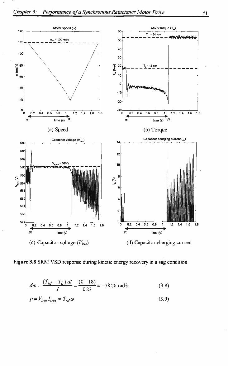
Chapter 3: Performance of a Synchronous Reluctance Motor Drive 51
140 Motor speed (co)
120
100
5" 80
60
-i 1 r-
«•>„.= 120 rad/s
40
20 r
0'-0 0.2 0.4 0.6 0.8 1 1.2 1.4 1.6 1.8
< • (s)
589
time (s) (e)
(a) Speed
Capacitor voltage (y^
60
50
40
30
E1 20
s. *w
0
-10
-20
-30
Motor torque (T^,)
TlT = 54 Nm
•
-
•
*tf) TL = 18Nm
lWw*/WiuM4^ ^^^^MH^
1
itfbu^UbUlklMiiML
-
•
-
-
•
•
0 0.2 0.4 0.6 0.8 1 1.2 1.4 1.6 1.8
< • (s) time(s) (e)
(b) Torque
Capacitor charging current (I J
12
10
^ 8
6
4
2
0 I
, I HI 111 I I I I '
i Jill 1 III | III '
time (s)
(c) Capacitor voltage (Vbus)
0 0.2 0.4 0.6 0.8 1 1.2 1.4 1.6 1.8
< • (s) time (s)
(d) Capacitor charging current
Figure 3.8 S R M V S D response during kinetic energy recovery in a sag condition
J 0.23
P = Vbus1 out = TM®
(3.8)
(3.9)

Chapter 3: Performance of a Synchronous Reluctance Motor Drive 52
where,
TM - motor torque
71 - load torque
J - system inertia
p - power applied to the motor terminals
Vbus - capacitor voltage
lout - current output from the dc bus to the motor
co -motor speed
When the sag is over, normal speed control operation is resumed with the motor
accelerating under torque limit towards the set speed. The large current pulse which was
observed in /,„ at the end of the sag during the trials without any control modifications
(refer Figure 3.5(a)) are not present n o w (Figure 3.8(d)).
From the above simulation results, it is verified that the VSD can over-ride a voltage sag
by recovering the kinetic energy available in the rotating mass. As mentioned in Section
3.2, here the ride-through behaviour was studied by applying a three-phase sag. From the
observed response, it is not difficult to infer the V S D behaviour during other sag
conditions when controlled by this strategy. It may be recalled from Subsection 2.2.1 that,
the set point for the bus voltage controller during a sag is 1 0 0 % of the nominal dc bus
voltage. Since the bus voltage (Vbus) is maintained constant at the nominal level, the
rectifier diodes are reverse biased during the entire sag duration. With this type of dc
voltage control by utilising the energy from the motor, the rectifier operation and hence
the dc bus characteristics would not be any different in the case of a single-phase sag or
with different sag magnitudes. Hence, it can be concluded that, this proposed control
strategy will provide the same type of sag ride-through performance for both single-phase
and three-phase sags and for all sag magnitudes. Since a sag ride-through can be achieved
only until the motor speed is above the cut-off limit, longer ride-through times can be
expected by this strategy if the initial motor speed is high and/or the load on the motor is
less.

Chapter 3: Performance of a Synchronous Reluctance Motor Drive 53
3.5 OPERATION UNDER A SAG AT LOW SPEEDS - BUS VOLTAGE
CONTROL BY RECOVERING MAGNETISING ENERGY
At low speeds (i.e. below 15.7 rad/s), since the kinetic energy present in the rotating mass
is relatively small, this strategy aims to recover the magnetising energy (jLI2) present in
the motor winding inductances in order to maintain the dc bus voltage at the required
level. This corresponds to Control Situation 3 as defined in Subsection 2.2.2. In this
situation, the torque reference is kept as zero and the magnetising current reference (/«*•*/)
is controlled (reduced) by the Bus Voltage Controller 2. The S R M behaviour under this
strategy can be analysed again by using equations (3.2) to (3.4) which were referred to in
the previous section. With the torque producing current isq maintained at zero value, a
reduction in the magnetising current iSd would reverse the polarity of the applied voltage
VSd and thus the direction of flow of the dc current lout would be reversed from the inverter
to the dc bus which charges the dc bus capacitor. The tuning of Bus Voltage Controller 2
is described in Appendix H. In this section, the low speed performance of the proposed
strategy on an S R M V S D will be analysed.
Simulation conditions: A 50% three-phase sag is applied for 1 second on the SRM VSD
operating at steady-state at a speed of 12 rad/s and a load torque of 18 N m with other
simulation conditions maintained as in the previous trials.
SRM VSD response: The response of the SRM speed (co), magnetising current (/*/),
capacitor voltage (VbUs) and the capacitor charging current (/,„) during the bus voltage
control by recovering the magnetising energy is shown in Figures 3.9 (a) to (d)
respectively. As soon as the sag is sensed, the motor torque is maintained at zero level.
The magnetising current, which is shown in Figure 3.9(b), is found to reduce in small
steps to zero in a short duration and during this interval, the dc bus voltage is found to be
controlled close to the set reference. Once the energy available in the motor winding
inductances is recovered completely there is no further transfer of energy between the
V S D and the motor (i.e. isd = isq= 0) and the dc bus capacitor voltage remains close to the

Chapter 3: Performance of a Synchronous Reluctance Motor Drive 54
20
10
0
-10
| "20 n
3 -30
-40
-50
-60
-7n
Motor speed (a>)
mr.l
•
= 12 rad/s 1 '
/ •
/ ' /
/
'
-
•
0 0.2 0.4 0.6 0.8 1 1.2 1.4 1.6 1.8
< • (s> time (s) W
(a) Speed (co)
10 Magnetising current (isd)
* » < •
-2
— I 1 1 • — i (—
i»<iWil«IWi'MI>J«'Ml'»»><
0 0.2 0.4 0.6 0.8 1 1.2 1.4 1.6 1.8
< •,. time (s) (e)
(b) Magnetising current (isj)
640
630
620
610
Capacitor voltage (V^)
>S 600
590
580
570-
—i 1 r~ -1 r—
0 0.2 0.4 0.6 0.8 1 1.2 1.4 1
< •, , <s) time (s) (e;
(c) Capacitor voltage (Vbus)
6 1.8
18
16
14
12
10
8
6
4
2
0
Capacitor charging current (I J
|
1
•
•
•
-
liil l ' , • H U W
0 0.2 0.4 0.6 0.8 1 1.2 1.4 1.6 1.8
< • (s) time (s) (e)
(d) Capacitor charging current (Iin)
Figure 3.9 S R M V S D characteristics during recovery of magnetising energy
nominal level (586 V). The motor speed is found to drop to zero and then reverse as
observed in Figure 3.9(a). This speed reversal happens only in types of loads such as
Chapter 3: Performance of a Synchronous Reluctance Motor Drive 55
hoists or cranes which can rotate the motor shaft even without any power applied. In the
case of frictional or fan type loads, the motor will halt after reaching zero speed. O n ac
supply returning to normal, the motor flux (/«/) builds up to the rated value and the V S D is
able to resume the speed control operation. The capacitor charging current (/,„) is found
to be within acceptable levels as found in Figure 3.9(d). A rise in the dc bus voltage is
observed in Figure 3.9(c), when the motor re-accelerates at speeds below zero because of
the regenerative operation. This voltage rise will be observed only in the case of loads
such as cranes and hoists and it can be discharged in the pre-charge resistor which is
present in a standard V S D .
As discussed in the case of bus voltage control by kinetic energy recovery (Section 3.4), in
the present control mode also the rectifier diodes are reverse biased during a sag and
hence the sag ride through performance will not be affected by the sag type and the sag
magnitude. Moreover, the fact that the capacitor voltage remains at the rated value even
after recovering the entire energy in the motor suggests that this strategy can be employed
for sags of duration longer than the applied duration in this simulation work (1 second).
Also, as observed from the simulation results, this sag ride-through control is applicable
even at zero speeds.
3.6 COORDINATED VSD CONTROL AT ALL SPEEDS
In the previous sections, the results from both modes of the proposed control strategy,
viz. recovery of the kinetic energy at high motor speeds and the magnetising energy at
lower speeds, were illustrated independently. It is seen that, the dc link characteristics in
the V S D are improved during a sag condition and the V S D will be able to ride-through
sags at both high and low motor speeds. These two operations can be combined with a
smooth transition of control at the cut-off speed so that the S R M will be able to ride-
through voltage sags at all ranges of speed including zero. In this section, the S R M V S D
performance will be discussed at an intermediate speed where the transition of control is
observed.

Chapter 3: Performance of a Synchronous Reluctance Motor Drive 56
Motor speed (o>)
0 0.2 0.4 0.6 0.8 1 1.2 1.4 1.6 1.J
60
50
40
30
? 20 z ? 10
-10
-20
-30
-40
KE
«
k If \
\
.
Motor torque (T,)
T^-atKhi
T^-laNm
ME
-
.
•
10
time (s) * >
(a) Speed (co) Magnetising current ((,„)
0 0.2 0.4 0.6 0.8 1 1.2 1.4 16 18 .!« " —•,. (s) time(s) («)
(b) Torque (TM)
< J 4
KE
•4 •
N W n W M i h f r t
25
20
15
Capacitor charging current flj
0 0.2 04 0.6 08 1 1.2 14 16 1.8 ls) time (s) <e>
(c) Magnetising current (iSd)
596, . ,
| KE ME
* •"* H
0 J3.2 04 0.6 0.8 1 1.2 1.4 1.6 1.8 (s> time(s) W
(d) Capacitor charging current (/,„) Capacitor voltage (V,,,,)
594
592
590
588:
586
584
582
580
578
576
»
V ,= 587V
KE ME
-4 X M
0 0.2 0.4 0.6 0.8 1 1.2 1.4 1.6 1.8 J* :—TT*.-(s) time(s) W
(e) Capacitor voltage (Vbus)
Figure 3.10 Behaviour of S R M V S D during combined dc bus voltage control by
recovering both kinetic and magnetising energy
Chapter 3: Performance of a Synchronous Reluctance Motor Drive 57
Simulation conditions: The inverter switching and sampling frequencies are set as
previously (5 kHz and 30 kHz respectively). The initial steady state motor speed is set at
60 rad/s operating at a load torque of 18 Nm. The V S D performance during this
combined control strategy is analysed by applying a 5 0 % three-phase sag.
SRM VSD response: The characteristics of SRM during the combined operation, viz.
speed (co), torque (7^), magnetising current (isd), capacitor charging current (/,-„) and the
capacitor voltage (Vbus) are shown in Figures 3.10(a) to (e). The sag condition is indicated
as in previous trials and the kinetic and magnetising energy recovery periods are indicated
as 'KE' and 'ME' respectively. It can be seen that the bus voltage is maintained at the set
reference by initially recovering the kinetic energy until the motor speed is above the cut
off speed (15.7 rad/s) and then by recovering the energy available in the inductances (by
reducing iSd). The motor speed is found to drop more rapidly during the regenerative
operation and then coast at a slower rate during the energy recovery from the motor
windings. Oscillations are observed in the motor torque response because of the non
linear relationship between torque and the bus voltage, i.e. the torque requirement
increases as the motor speed decreases in order to maintain the dc bus voltage constant.
Once the supply returns to normal, the motor flux reaches its rated level and the motor
starts to accelerate towards the set speed. The capacitor charging current (/,„) is found to
be within acceptable limits on normal supply recovery.
3.7 EFFECT OF LOWERING THE BUS CAPACITANCE
It was shown that, by recovering magnetising energy, the voltage sag ride-through
performance can be achieved for longer durations, but while doing so, the motor speed
either falls to zero or reverses. As discussed in Sections 3.1 and 3.4, during kinetic energy
recovery, the rate of motor speed drop and hence the voltage sag ride-through duration of
the V S D can be improved if the amount of kinetic energy recovered can be reduced. The
kinetic energy recovered by the V S D control system is utilised in two ways, viz. (a) fed
Chapter 3: Performance of a Synchronous Reluctance Motor Drive
back to the motor in order to compensate the losses in the motor windings and (b) to
trickle charge the capacitor in order to maintain the dc voltage at the required level. Since
sag ride-through performance with less speed drop is desired, the effects of smaller dc bus
capacitance on the performance of this control strategy, particularly during kinetic energy
recovery, will be studied in this section.
Simulation conditions: Simulation trials, as in Section 3.6, were repeated for bus voltage
control by recovering both sources of energy available in the motor. Here the bus
capacitance value ( Q is reduced to one-fourth the earlier value (i.e. 250 uF instead of
1000 uF). The bus voltage regulators are suitably tuned to accommodate the change in C
and the tuning details of the bus voltage controllers are presented in Appendix H.
SRM VSD response: The behaviour of SRM speed, torque, magnetising current,
capacitor charging current and capacitor voltage (VbUs) with reduced C are shown in
Figure 3.11(a) to (e). It can be seen that the S R M speed response has not changed
significantly from the earlier trials with a large bus capacitance (Section 3.6). In other
words, sag ride through duration is found to be unaffected by the variation in C. As in the
earlier trials, the motor torque reverses during the recovery of kinetic energy in order to
supply the dc bus until the motor speed reaches below the cut-off speed limit (15.7 rad/s).
At motor speeds below 15.7 rad/s, the flux in the motor is recovered and the dc bus
voltage is maintained at the set level. Since the ride-through performance during kinetic
energy recovery is of interest here, the dc current hut, which shows the combined
characteristics of the current recovered from the motor by regeneration as well as the
current supplied to the motor in order to maintain the flux at the rated value, was studied
in further detail. It was observed that, during the bus voltage control by recovering the
kinetic energy, the average value of hut is found to be around zero for both capacitor
values, which implies that the energy recovered from the motor is utilised to mainly
compensate for the losses in the motor windings. Since the capacitor voltage is maintained
at the rated dc voltage by this control strategy, only a negligible current is drawn by the
capacitor. In this simulation, the capacitor losses were not modelled. But even in practical
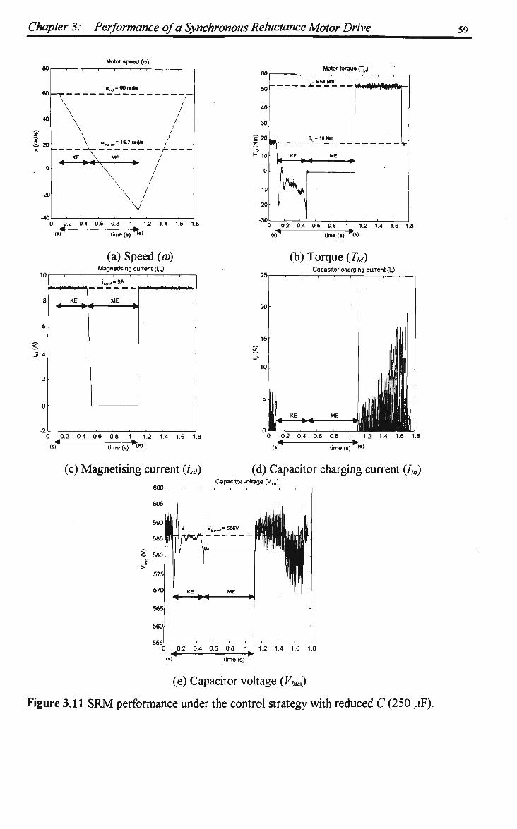
Chapter 3: Performance of a Synchronous Reluctance Motor Drive 59
Motor speed (<o)
» = 60 rad/s
10
time (s) <e>
(a) Speed (co) Magnetising current (i^)
ll( HWIHWIWIIM-U,= 9A
KE
< •
0 J).2 0.4 0.6 0.8 1^ 1.2 1.4 1.6 1.8
(s) time (s) <e)
60
50
40
30
?20
^lO
0
-10
-20
1 in If*
3 0.2
(s)
Motor torque (T^
TL-18Nm
KE ME
\ '
•
•
T
.
0.4 0.6 0.8 1
time(s) *"<
1.2 1.4 1.6 1
»>
(b) Torque (TM) Capacitor charging current flj
time (s) <e)
(c) Magnetising current (isd) (d) Capacitor charging current (/,„)
600 Capacitor voltage (V,,,,,)
<- 580
time (s)
(e) Capacitor voltage (Vbus)
Figure 3.11 SRM performance under the control strategy with reduced C (250 uF).

Chapter 3: Performance of a Synchronous Reluctance Motor Drive 60
VSDs, when the dc link voltage is maintained constant, very little trickle charging current
flows into the capacitor, which is negligible compared to the energy lost in the motor
windings. Hence, it can be stated that, the sag ride-through duration, when controlled by
this strategy, is not influenced by the variation in the capacitor size. But, with a smaller C,
the dc voltage ripple and the capacitor charging current are found to increase (as observed
in Figures 3.10 and 3.11).
3.8 SUMMARY
In this chapter, the performance of an SRM VSD was studied under normal power supply
conditions as well as during voltage sags. It was observed that, during a sag, the dc under-
voltage and ac over-current faults are the main causes of V S D tripping and the impact of a
three-phase sag is more severe on the V S D performance than a single-phase sag. The
intended control strategy of maintaining the dc bus voltage at the rated value during a sag
was separately demonstrated by recovering the kinetic energy at higher speeds and the
magnetisation energy at lower speeds. Then, the performance was verified at an
intermediate speed by combining these two control modes where a smooth control
transition was observed at the cut-off speed. The under-voltage and over-current fault
situations were not observed when controlled by this proposed strategy. The main
advantage of this strategy is its ability to ride-through a single-phase as well as a three-
phase sag and all sag magnitudes with identical performance and its ability to provide a sag
ride-through even at zero motor speed.
61
CHAPTER 4
PERFORMANCE OF AN INDUCTION MOTOR DRIVE
4.1 INTRODUCTION
Induction motors (IMs) are the work horses of many industrial processes and are the most
commonly used type of electric motors. They are preferred over other motor types
because of their simpler and rugged construction and easier maintainability. But their
characteristics are different from those of synchronous machines which make the control
of IMs more complicated. The synchronous motors operate at a speed governed precisely
by the supply frequency whereas the speed of the IMs involve a slip, which varies with the
load on the motor. The tracking of the flux position is very important for the field oriented
control of ac motors [26] which can be done easily in the case of synchronous motors with
the help of position sensors (or indirect position sensing algorithms) whereas in the case of
IMs, more complicated computations are involved. The angular relationships of flux
position with respect to the stationary reference frame and their significance on the control
of IMs are described in Appendix B and Subsection 2.3.1 respectively. In this chapter, the
performance of the proposed strategy will be studied on an I M V S D . The control of IM
V S D is simulated in M A T L A B ™ on the basis of the model explained in Section 2.3.1.
Initially, the performance of the VSD model will be verified for normal operation under
ideal ac supply conditions. Then, the response of the I M V S D when subjected to three-
phase as well as single-phase sags will be presented. From the simulation results, the
reasons for V S D tripping during a voltage sag condition will be analysed. Finally, the
voltage sag ride-through performance of the control strategy, viz the dc bus voltage
control by recovering the energy from the rotating mass at high motor speeds and from the
motor winding inductances at low speeds, will be presented. From the simulation results, it
is observed that, the first mode of the control strategy, viz. kinetic energy recovery from
Chapter 4: Performance of an Induction Motor Drive 62
the rotating mass, works satisfactorily as in the case of an SRM, whereas, the dc bus
capacitor voltage control by recovering the energy from the inductances is found not to
work satisfactorily as envisaged by the control strategy. The reasons for this behaviour
will be analysed. A n improved ride-through control of induction motors at low speeds is
suggested and the results will be analysed. Since, it was found in the case of an S R M V S D
that the sag ride-through duration is not affected by the variation in the dc bus capacitance
values when controlled by the proposed strategy, this study is not repeated here. As in the
case of the S R M V S D , simulation results are presented here for constant torque loads and
the sag ride-through performance results for fan type loads are shown in Appendix J.
4.2 NORMAL SPEED CONTROL OPERATION OF AN EVI VSD
In this section, the behaviour of an EVI V S D under ideal power supply conditions as well
as on voltage sag conditions (both single-phase and three-phase types) will be examined.
From the results, the reasons for the V S D tripping in a sag situation will be analysed.
4.2.1 PERFORMANCE UNDER NORMAL OPERATING CONDITIONS - NO
SAG
Here, the behaviour of an IM VSD during acceleration and steady state speed control
under ideal ac supply conditions (Control Situation 1 as defined in Subsection 2.2.2) is
shown. In this situation, the speed controller generates an appropriate torque reference in
order to maintain the motor speed at the set value. The motor parameters are shown in
Appendix E and the details of the Speed Controller tuning are explained in Appendix G
Simulation conditions: The VSD is simulated with a nominal balanced power supply, as
shown in Figure 3.1. The inverter switching frequency is kept at 5 kHz and accordingly
the sampling frequency is chosen as 30 kHz in order to take account of every switching
transition as explained in Subsection 3.3.1. A speed reference (core/) of 120 rad/s is applied
with flux reference at the rated value (i.e. imRref= 9 A). The load torque (TL) and the torque
limit (TLT) are set at 5 0 % and 1 5 0 % respectively of the rated motor torque (36 N m ) .

Chapter 4: Performance of an Induction Motor Drive 63
n
8
140
120
100
80
60
40
20
Motor speed to)
A
0 0.2 0.4 0.6 0.8 1 1.2 1.4 1.6 1.1
I '• time (s)
(a) Speed (co) Magnetising current ( „)
1 Q i i i i i i i i
ilrRl- = 9A
•I • *-0 0.2 0.4 0.6 0.8 1 1.2 1.4 1.6 1.8
time (s)
(c) Magnetisation current (/„/?)
30
m mmmmtm so
•30
Motor lorque IT J
TL = 18Nm I
M M M M M M M D -
• o < T i 0 4 ol 51 i Ti v* vs ii (0 time(s)
(b) Torque (TM) Flux producing current ( q)
6.
_£•
4.
3
2
1
0 0.2 0.4 0.6 0.8 1 1.2 1.4 1.6 1.8
time (s)
(d) Stator d-axis current (isd) Torque producing current (y
, MMMMNMKU***. 2e
20
1C
f I I I I I I '
mm**iHMmmnm
0 0.2 0.4 0.6 0.8 1 1.2 1.4 1.6 1.8 (t) time (s)
(e) Stator q-axis current (isq)
Figure 4.1 IM VSD during normal ac supply conditions
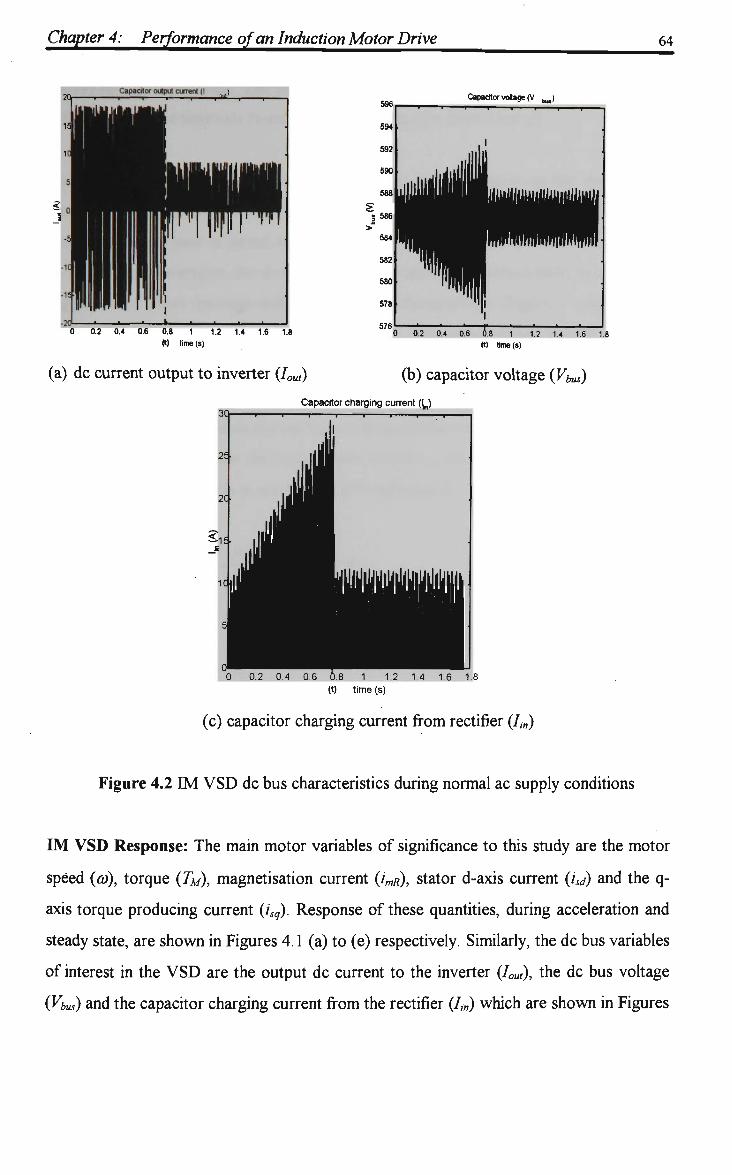
Chapter 4: Performance of an Induction Motor Drive 64
596 Capacitor vo«age(V . 1
(a) dc current output to inverter (hut) (b) capacitor voltage (Vbus)
^ ^ ^ ^ ^ Capacitor charging current (L)
(c) capacitor charging current from rectifier (/,„)
Figure 4.2 I M V S D dc bus characteristics during normal ac supply conditions
I M V S D Response: The main motor variables of significance to this study are the motor
speed (co), torque (TM), magnetisation current (imR), stator d-axis current (/«/) and the q-
axis torque producing current (isq). Response of these quantities, during acceleration and
steady state, are shown in Figures 4.1 (a) to (e) respectively. Similarly, the dc bus variables
of interest in the V S D are the output dc current to the inverter (hut), the dc bus voltage
(Vbus) and the capacitor charging current from the rectifier (/,„) which are shown in Figures
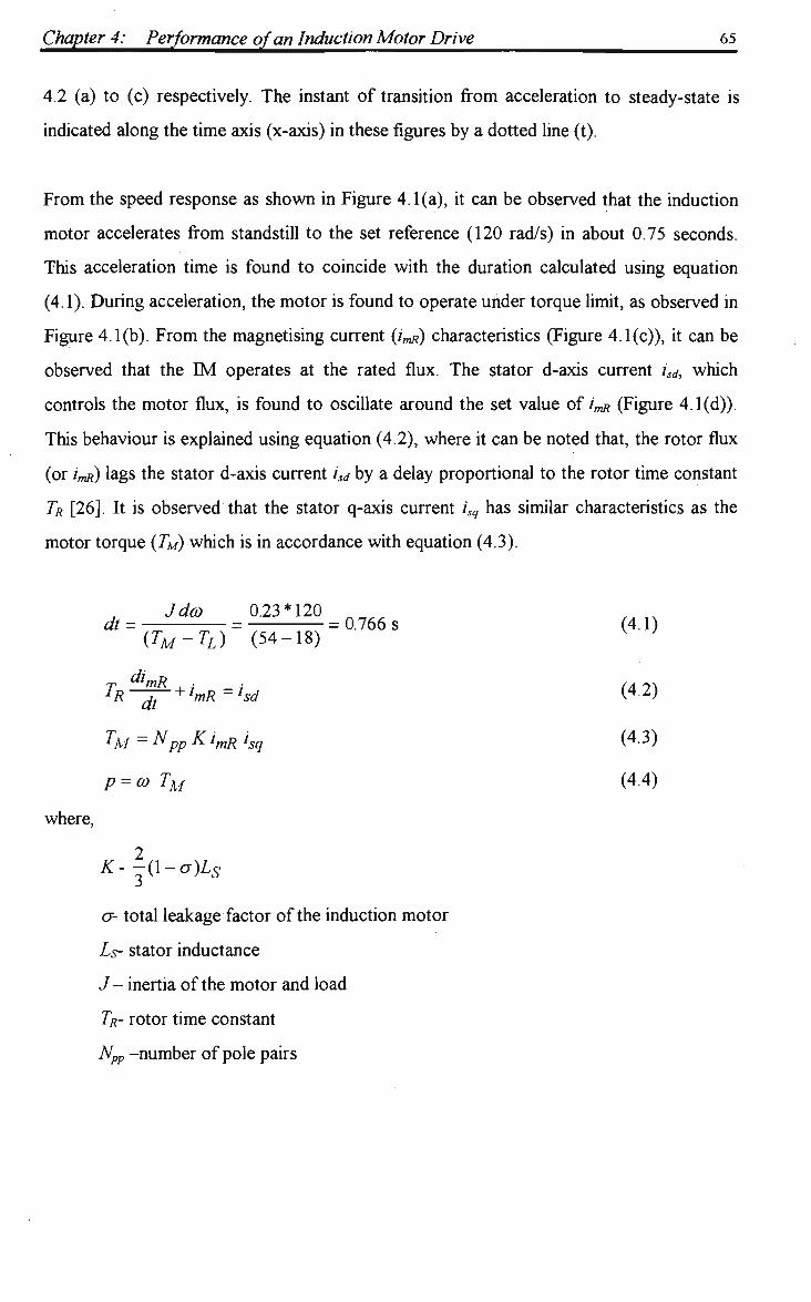
Chapter 4: Performance of an Induction Motor Drive 65
4.2 (a) to (c) respectively. The instant of transition from acceleration to steady-state is
indicated along the time axis (x-axis) in these figures by a dotted line (t).
From the speed response as shown in Figure 4.1(a), it can be observed that the induction
motor accelerates from standstill to the set reference (120 rad/s) in about 0.75 seconds.
This acceleration time is found to coincide with the duration calculated using equation
(4.1). During acceleration, the motor is found to operate under torque limit, as observed in
Figure 4.1(b). From the magnetising current (i^) characteristics (Figure 4.1(c)), it can be
observed that the I M operates at the rated flux. The stator d-axis current isj, which
controls the motor flux, is found to oscillate around the set value of i„R (Figure 4.1(d)).
This behaviour is explained using equation (4.2), where it can be noted that, the rotor flux
(or /m/O lags the stator d-axis current isd by a delay proportional to the rotor time constant
TR [26]. It is observed that the stator q-axis current isq has similar characteristics as the
motor torque (TM) which is in accordance with equation (4.3).
(4.1)
(4.2)
(4.3)
(4.4)
Jdco 0.23*120 nt (TM-TL) (54-18)
T dimR+i iR df
+lmR-]sd
TM = Npp K 'mR lsq
p = co TM
K-^(\-o)Ls
-- 0.766 s
cr- total leakage factor of the induction motor
Ls- stator inductance
J- inertia of the motor and load
TR- rotor time constant
Npp -number of pole pairs
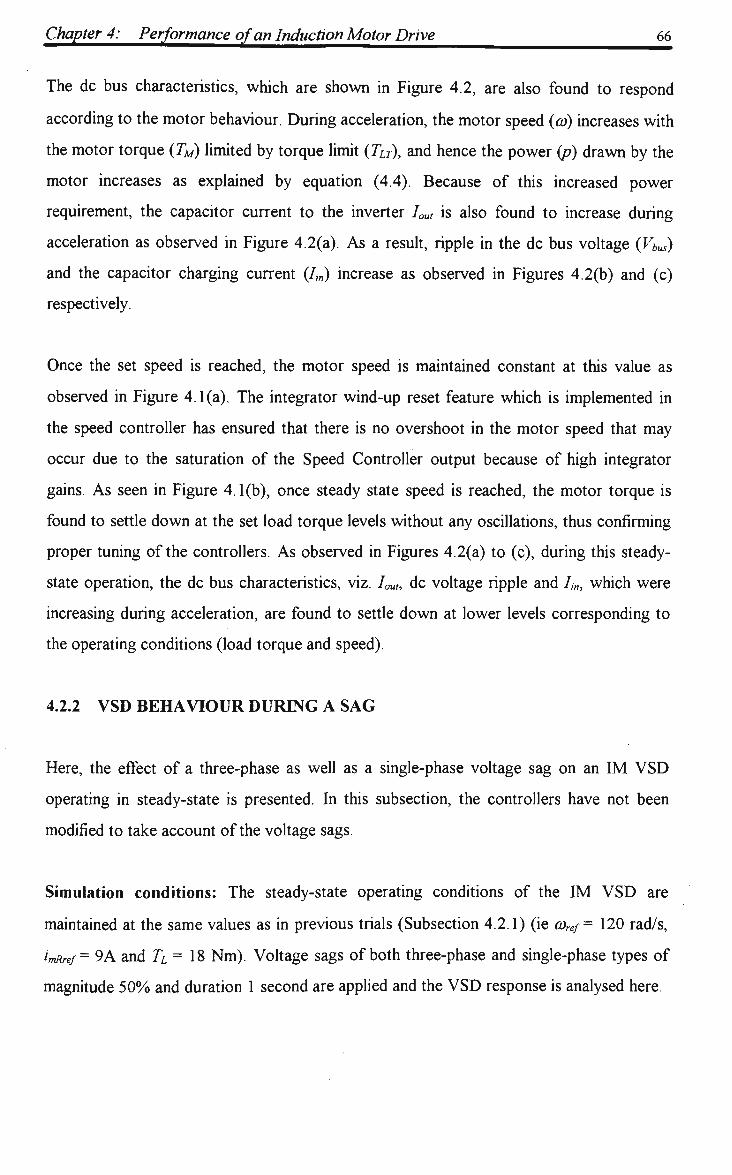
Chapter 4: Performance of an Induction Motor Drive 66
The dc bus characteristics, which are shown in Figure 4.2, are also found to respond
according to the motor behaviour. During acceleration, the motor speed (co) increases with
the motor torque (TM) limited by torque limit (TLr), and hence the power (p) drawn by the
motor increases as explained by equation (4.4). Because of this increased power
requirement, the capacitor current to the inverter I^t is also found to increase during
acceleration as observed in Figure 4.2(a). As a result, ripple in the dc bus voltage (Vbus)
and the capacitor charging current (/,„) increase as observed in Figures 4.2(b) and (c)
respectively.
Once the set speed is reached, the motor speed is maintained constant at this value as
observed in Figure 4.1(a). The integrator wind-up reset feature which is implemented in
the speed controller has ensured that there is no overshoot in the motor speed that may
occur due to the saturation of the Speed Controller output because of high integrator
gains. As seen in Figure 4.1(b), once steady state speed is reached, the motor torque is
found to settle down at the set load torque levels without any oscillations, thus confirming
proper tuning of the controllers. As observed in Figures 4.2(a) to (c), during this steady-
state operation, the dc bus characteristics, viz. hut, dc voltage ripple and /,„, which were
increasing during acceleration, are found to settle down at lower levels corresponding to
the operating conditions (load torque and speed).
4.2.2 VSD BEHAVIOUR DURING A SAG
Here, the effect of a three-phase as well as a single-phase voltage sag on an IM VSD
operating in steady-state is presented. In this subsection, the controllers have not been
modified to take account of the voltage sags
Simulation conditions: The steady-state operating conditions of the IM VSD are
maintained at the same values as in previous trials (Subsection 4.2.1) (ie coref= 120 rad/s,
imRref- 9 A and 71 = 18 N m ) . Voltage sags of both three-phase and single-phase types of
magnitude 5 0 % and duration 1 second are applied and the V S D response is analysed here.

Chapter 4: Performance of an Induction Motor Drive 67
900
800
700
600.
500>
400
300
Capacitor Voltage (V^)
200
1 L 0 J)2 0.4 0.6 0.8 1^ 1.2 1.4 1.6 1.8
(s) * (e) time (s)
eon
500
400
300
200
100
n
Capacitor charging current ( y
•
•
•
0 jQ.2 0.4 0.6 0. 8 V 1.2 1.4 1.6 1.8
(«) (e) time (s)
(a) Capacitor Voltage (Vbus) (b) Capacitor charging current (/,„)
Figure 4.3 D C bus characteristics during a three-phase sag
605 Capacitor Voltage (V^)
565
40
35
30
25
2 20
15
10
5
n I
Capacitor charging current ( y
•
•
•
jUUuUUUu^
•
0 0.2 0.4 0.6 0 8 1 1.2 1.4 1.6 1.8 0 0.2 0.4 0.6 0.8 1 1.2 1.4 1.6 1.8 (e)
time (s) (s) •(.)
time (s)
(a) Capacitor Voltage (Vbus) (b) Capacitor charging current (/,„)
Figure 4.4 D C bus characteristics during a single-phase sag

Chapter 4: Performance of an Induction Motor Drive 68
EM VSD Response: In the presence of both three-phase and single-phase sags, the motor
speed and torque responses were unaffected from the steady state behaviour with normal
ac supply conditions (Figure 4.1(a) and (b)). The motor flux was maintained at the rated
value. Because the motor torque and speed were maintained constant, the current drawn
out of the dc capacitor (hut) was found to be the same as during the steady-state condition
in a no sag situation (as in Figure 4.2(a)). However, the capacitor voltage (Vbus) and the
capacitor charging current from the rectifier (/,„) are the quantities that are significantly
affected by the voltage sags which are shown in Figures 4.3 and 4.4 for a three-phase and
a single-phase sag respectively. The start and end of the sag are indicated in these figures
as previously.
In the case of a three-phase sag, the rectifier diodes are initially reverse biased and hence
there is no flow of charging current (/,„) to the capacitor as observed in Figure 4.3 (b).
N o w the capacitor discharges to supply the inverter in order to keep the motor operating
at the set conditions and hence the capacitor voltage VbUs is found to drop as observed in
Figure 4.3 (a). This discharging operation continues until Vbus becomes equal to the peak
of the line-to-line ac supply voltage during the sag. O n Vbus reaching this new level, the
rectifier output current (/,„) starts flowing into the capacitor as in the case of a normal ac
supply condition and the bus voltage is maintained during the sag. The drop in the
capacitor voltage increases with sag magnitude and load torque. W h e n the ac supply
voltage returns to normal, a very high capacitor recharging current (//„) results as observed
in Figure 4.3(b). This magnitude of the current transient depends on the sag magnitude
and in spite of being limited by the circuit impedances, it is usually much higher than the
rating of the rectifier diodes. Because of this rapid charging of the capacitor, Vbus is found
to overshoot to higher levels and then returns to the nominal level by discharging to supply
the motor load as observed in Figure 4.3 (a).
In the case of a single-phase sag, the capacitor is charged by the unaffected line-to-line
voltage peaks and it discharges during the rest of the supply cycle. D u e to this intermittent
charging pattern, the ripple in the dc voltage Vbus and the charging current /,„ are found to
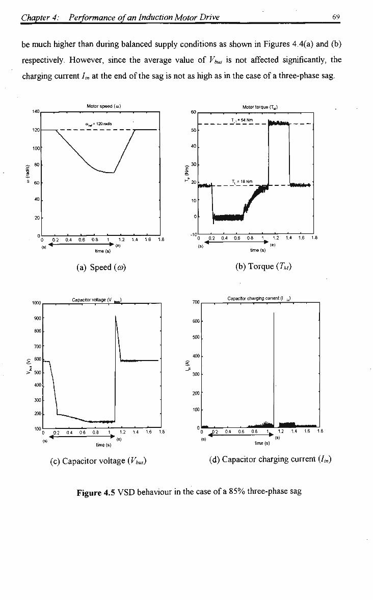
Chapter 4: Performance of an Induction Motor Drive 69
be much higher than during balanced supply conditions as shown in Figures 4.4(a) and (b)
respectively. However, since the average value of Vbus is not affected significantly, the
charging current /,„ at the end of the sag is not as high as in the case of a three-phase sag.
140 Motor speed (co)
time (s)
(a) Speed (co)
RO
50
40
30
20
10
0
Motor torque (TM)
TLT=54Nm
•
• , TL=18Nm IW^W* "* ~~ ~~ ~~ ~~ ™~ •" ~dtfflfl
•
•
•
_......
f • i . . — > — i — • — i —
0 0.2 0.4 0.6 0.8 1 1.2 1.4 1.6 1.8
time (s)
(b) Torque (TM)
1000
900
800
700 (A)
> 500
400
300
200
Capacitor voltage (V ,„,)
• u _
\
\
•
0 0 2 04 06 0 8 1 1.2 1.4 1.6 1.8
(s) (e' time (s)
(c) Capacitor voltage (Vbus)
700
600
500
400
200
100
n
Capacitor charging current (I J
'
•
•
0 J0.2 0 4 0.6 0A V 1.2 1.4 1.6 1.1
(s) time (s)
(e)
(d) Capacitor charging current (/,„)
Figure 4.5 V S D behaviour in the case of a 8 5 % three-phase sag

Chapter 4: Performance of an Induction Motor Drive 70
As the magnitude of the sag increases further, its impact on the VSD performance also
increases. In the case of single-phase sags, the torque and speed performance of the V S D
is not affected for all sag magnitudes, whereas the dc voltage ripple and capacitor charging
current Iin are found to increase further. However, when subjected to a three-phase sag of
very high magnitude, the motor speed and torque are also found to be affected.
The response of the IM VSD, when subjected to a balanced three-phase sag of magnitude
8 5 % and duration 1 second with similar operating conditions as in the previous case is
shown in Figure 4.5. The motor is found to operate at the set speed and torque values for
a small duration after the sag occurrence (Figure 4.5(a)). During this time, the dc bus
capacitor discharges to supply the load and there is no charging current Iin from the
rectifier as observed in Figures 4.5 (c) and (d). Below a certain dc voltage (around 200 V ) ,
the capacitor does not have the energy required to drive the motor at the set speed and
torque conditions and hence the motor speed is found to drop below the set reference as
observed in Figure 4.5 (a). In this period, no torque is developed by the motor as found in
Figure 4.5 (b). The capacitor n o w discharges just enough to maintain the motor flux and
the rate of discharge is found to be lower than during normal motoring condition (Figure
4.5 (c)). This operation continues until Vbus becomes lower than the ac supply peaks when
the capacitor charging current /,„ starts flowing from the rectifier and the V S D is able to
supply the required power to the motor. The motor speed is maintained at this lower level
until the normal ac supply returns. The speed drop during the sag varies depending on the
motor operating torque (TM) and the dc bus voltage Vbu., as per equation (4.5). Once the
supply returns to normal condition, the motor is found to accelerate to the set speed under
torque limit. However, a large recharging current pulse appears in /,„ because of the lower
capacitor voltage during the sag. This high capacitor charging results in overshoot of Vbm
which then returns to the nominal value by discharging to the load.
p = co TM = VbusIout (4.5)
where
p - power input to the motor,
lout - the dc current from the capacitor to the inverter.

Chapter 4: Performance of an Induction Motor Drive 71
4.2.3 REASONS FOR VSD TRIPPING ON A SAG CONDITION
From the simulation results, it can be observed that both three-phase and single-phase sags
affect the V S D performance, especially the dc bus characteristics, with the impact of a
three-phase sag being more severe than a single-phase sag.
When subjected to a three-phase voltage sag, the dc bus capacitor voltage reaches a lower
level, depending on the sag magnitude and the load and this can lead to a V S D trip due to
an under-voltage fault. Also, when the ac supply returns to normal, a very high recharging
current Iin occurs which can cause damage to the rectifier diodes. During such conditions,
the over-current trip protection in the V S D can cause nuisance tripping. The speed drop
that was observed in the case of very high three phase sags is not a major cause of concern
for many V S D applications where process continuity rather than occasional speed
reduction is critical.
In the case of single-phase sags, the drop in the capacitor voltage Vbus is not as much as in
a three-phase sag condition, but a very high ripple content is present in Vbus which
increases with the sag magnitude and load on the motor. Hence, an under-voltage trip can
occur during deeper single-phase sags. Similarly, the high capacitor charging current /,„
that occur during such deep sags can cause an ac over-current trip.
4.3 OPERATION UNDER A SAG AT HIGH SPEEDS - BUS VOLTAGE
CONTROL BY RECOVERING KINETIC ENERGY
In this section, the performance of an IM VSD with dc bus voltage control by recovering
the kinetic energy available in the rotating mass is demonstrated. It may be recalled from
the definitions of the proposed control strategy (Section 2.2) that this mode is employed
only at higher motor speeds (above 1 0 % of the motor base speed) because the kinetic
energy available in the motor at lower speeds is relatively negligible. This, corresponds to

Chapter 4: Performance of an Induction Motor Drive 72
Control Situation 2 as defined by the control strategy and during this interval, the Bus
Voltage Controller 1 sets the motor torque reference with the Speed Controller bypassed.
The motor flux (or magnetising current i„R) is maintained at the rated value in order to
ensure proper operation of the induction motor as a generator. The bus voltage controller
reverses the torque reference appropriately so that the direction of torque producing
current isq is reversed which in turn reverses the flow of dc current lout from the motor to
the dc capacitor. This operation is similar to that of an S R M and is explained by equations
(4.6) to (4.8). The bus voltage controller (proportional-integral type), which monitors the
actual dc bus voltage against the set reference, ensures that only the required amount of
energy is recovered from the rotating mass in order to maintain the capacitor voltage at
the desired nominal value. The tuning details of the Bus Voltage Controller 1 are given in
Appendix G.
. _ 2(Vsdisd + Vsqixq)
Vsd=RJsd +oLs(^-comRisq) + (l-o)Ls^- (4.7)
V^q = Khq +crLs(-^- + comRisd) + (\-o)LscomRimR (4.8)
where,
Vsd, Vsq - d and q axis stator voltages
isd, isq - d and q axis stator currents
Rs - stator resistance,
Ls - stator inductance,
o- total leakage factor of the motor,
00^ - angular velocity of the magnetising vector, and
The VSD performance when controlled by this strategy at high motor speeds is discussed
here.

Chapter 4: Performance of an Induction Motor Drive 73
140 Motor speed (en)
i i 60
50
40
~30 E 2 K 20
10
0
Motor torque (T^
TIT = 54Nm
r
T^= 18 Nm
mmm**^
•
•
0 0.2 0.4 0.6 0.8 1 1.2 1.4 1.6 1.8 ° 0 2 0 4 0.6 0.8 1 1.2 1.4 1.6 1.8
Kl time(s) K' time(s)
(a) Speed (co) (b) Torque (7A/)
600
595
590
: 585
580
575
570
Capacitor Voltage (V^J 35
30
25
20
15
Capacitor charging current (IJ i i i i i i i
0 0.2 0.4 0.6 0.8 1 1.2 1.4 1.6 1.8
time (s) time (s) (e)
(c) Capacitor voltage (Vbw) (d) Capacitor charging current (/,„)
Figure 4.6 EVI V S D response during kinetic energy recovery at high motor speeds
Simulation conditions: A 5 0 % three-phase sag is applied to the V S D when the induction
motor is operating in steady state at 120 rad/s with half the rated load (18 N m ) with the
other operating conditions unchanged from previous trials (refer Section 4.2.2).

Chapter 4: Performance of an Induction Motor Drive 74
IM VSD Response: The response of the motor speed (eo), torque (TM), capacitor voltage
(Vbus) and capacitor charging current (/,„) during dc link voltage control utilising rotor
kinetic energy is shown in Figures 4.6(a) to (d) respectively. The sag period is indicated in
these figures as previously. The motor is found to operate at full flux throughout the sag.
From Figure 4.6(b), it is observed that the direction of motor torque reverses as soon as
the sag is sensed and it settles down at a very low negative value as controlled by the Bus
Voltage Controller 1. The capacitor voltage Vbus is found to reach its set point within a
few milliseconds and it is maintained at this value throughout the sag condition (refer to
Figure 4.6(c)). Because of this bus voltage control at the nominal level, the rectifier diodes
are reverse biased and hence, there is no flow of capacitor charging current /,„ during the
sag as found in Figure 4.6(d). From motor speed response, (Figure 4.6(a)), it is observed
that, the motor speed (co) reduces at a uniform rate during this regenerative control. A
speed drop of approximately 90 rad/s is observed during this 1 second sag which is more
than the speed drop (dco) that would have occurred during the same period, had the motor
coasted without any power applied from the V S D , which is calculated using equation
(4.9).
<to=(^-^)dr = (0^18) = J 0.23
where,
TM - motor torque,
TL - load torque,
J - inertia of the rotating mass
This confirms the usual motor behaviour that, the rate of speed drop during regeneration is
higher than during normal stopping. Also, it is observed that, as the motor speed drops,
the reverse torque increases, in order to meet the constant power required at the dc link.
O n ac supply recovery, the large transient in the recharging current /,„ which was found
earlier (refer Figure 4.3(b)) is not observed during this control.

Chapter 4: Performance of an Induction Motor Drive 75
From the above simulation results, it can be concluded that a sag ride-through
performance can be achieved using this strategy in the case of an I M V S D by utilising the
kinetic energy available in the rotating mass until the motor speed reaches a minimum
value. Also, the ride-through performance under varying sag conditions can be inferred
from the dc bus characteristics. As discussed in the case of an S R M (refer Section 3.4),
the rectifier diodes are reverse biased during this dc bus voltage control, and hence there is
no power flow from ac mains into the V S D . This condition holds good for both sag types
(single-phase as well as three-phase) irrespective of the sag magnitude. Hence, the
performance of this strategy will not be affected by the sag type and sag magnitude. Also,
since the motor speed drops in proportion to the load torque, longer ride-through times
can be achieved at reduced loads and at high motor speeds. This strategy is more suitable
in V S D applications where the operation continuity is of utmost importance and
occasional speed variations can be tolerated.
4.4 OPERATION UNDER A SAG AT LOW SPEEDS - BUS VOLTAGE
CONTROL BY RECOVERING MAGNETISING ENERGY
In this section, the performance results of the proposed strategy on an IM VSD during a
voltage sag are discussed at low motor speeds when it is attempted to recover the
magnetising energy in the motor windings for dc bus voltage control. This type of control
is desired at low motor speeds when the kinetic energy available in the motor is negligible
and it corresponds to Control Situation 3 as defined in the control strategy (Subsection
2.2.2). The motor torque is maintained at zero level and the flux (or imR) reference is
reduced by the Bus Voltage Controller 2. The same principle as envisaged in the case of
S R M is employed here, i.e. by maintaining motor torque at zero, the magnetising energy
available in the inductances can be recovered by reversing the polarity of the applied
voltage across the machine windings. However, it is observed that in an IM, the recovery
of energy from the winding inductances does not work in the same way as in the case of
an S R M . The performance results of the I M V S D under this strategy are analysed. The
tuning of the Bus Voltage Controller 2 is described in Appendix G.
Chapter 4: Performance of an Induction Motor Drive 76
Motor speed (u) Magnetising current (i^)
0 y0.2 0.4 0.6 Q-fl V 1.2 14 1-6 1.1
(a) Motor speed (co)
100
80
60
40
_ 2 0
<
-20
-40
-60
-80
Stator d-axis current (isd)
'«*«=9A
•
I
f •
0 0.2 0 4 0.6 0.8 1 1.2 14 1.6 1.8
a* •<•> time(s)
(b) Magnetising current (/„,*)
Capacitor output current (I M) 5 0 - 1 1 1 i 1 i i 1 —
0 0.2 0 4 0.6 0.8 1 1.2 1.4 1.6 1.8
.1* •(•) (») time(s)
(c) stator d-axis current (isd) Capacitor Voltage (V,^)
700
650
600
> >"
550
500
L
A L 1 l-~—
0 02 0.4 0.6 0.8 1 1.2 14 1.6 1.8
(s)" time(s)
(e) Capacitor voltage (Vbus)
(d) Capacitor current to inverter (hut) Capacitor charging current (i „p)
_L. 0—*—• — ' ' 0 0.2 0.4 06 0.8 1 1.2 14 1.6 1.8 < • > * - • > ( . )
time(s)
(f) Capacitor charging current (/,„)
Figure 4.7 I M V S D Response during attempted recovery of magnetising energy
Chapter 4: Performance of an Induction Motor Drive 77
Simulation condition: Here, an identical three-phase sag of magnitude 50% and duration
1 second is applied to the I M V S D when the motor is running in steady state at a speed of
12 rad/s with half the rated load (18 N m ) . The maximum and minimum limits for stator d-
axis current reference (isdrej) are set at 9 A and 0 A respectively.
IM VSD Response: The response of the HVI VSD, viz. speed (co), magnetisation current
(i^), stator d-axis current (isd), capacitor output current to the inverter (lout), capacitor
voltage (Vbus) and the capacitor charging current (/,„), are shown in Figures 4.7(a) to (f).
W h e n the sag is sensed, the magnetising current ( w ) is found to reduce to zero within a
few milliseconds as seen in Figure 4.7(b). W h e n the motor flux decreases, a high negative
current pulse (of about 80 A ) is observed in isd characteristics as seen in Figure 4.7(c).
From Figure 4.7(d), it is observed that, the dc current hut, instead of being fed back into
the capacitor, has been drawn out of the capacitor by the motor. This has resulted in the
reduction of capacitor voltage (Vbus) rather than it being maintained at the desired level as
seen in Figure 4.7(e). As a result, when normal ac supply returns, large current pulses are
observed in the capacitor charging current (/,„) as shown in Figure 4.7(f). During the sag
period, the motor speed is found to have coasted towards zero and reversed further as
seen in Figure 4.7(a). But this speed reversal, as explained in the case of the S R M ,
happens only in the case of loads such as hoists or cranes whereas with frictional loads, the
motor stops after reaching zero speed.
When the sag is over, the flux returns to normal rated value and the motor starts to
accelerate towards the set speed. The motor operates in regeneration mode until the motor
reaches zero speed and thereafter normal motoring operation starts. Because of this
regeneration, the capacitor voltage Vbus is found to increase to a higher value than normal.
This voltage can be discharged at the pre-charge resistors available in a standard V S D .
Obviously, it is clear from the simulation results that, the energy recovery from the
magnetising inductances has not worked with an I M V S D as envisaged by the control
strategy and the reasons for this behaviour are analysed further.
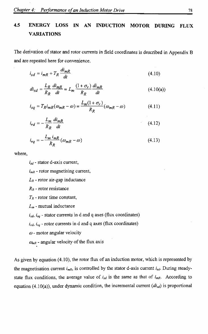
Chapter 4: Performance of an Induction Motor Drive 78
4.5 ENERGY LOSS IN AN INDUCTION MOTOR DURING FLUX
VARIATIONS
The derivation of stator and rotor currents in field coordinates is described in Appendix B
and are repeated here for convenience.
hd=imR+TR-^ (4.10)
Ai - LR dimR T (l + (Tr)dimR ,A ]n,. dlsd -Y~R~dT-
Lm ~lR~~dT (4-10(a))
isq = TRimR(^mR " ®) = "* p ^ (0)mR - Co) (4.11) KR
lrd~~RR dt (4-12)
irq=-^mB-(0JmR-C0) (4.13) KR
where,
isd - stator d-axis current,
imR - rotor magnetising current,
LR - rotor air-gap inductance
RR - rotor resistance
TR - rotor time constant,
Lm - mutual inductance
isd, isq - stator currents in d and q axes (flux coordinates)
hd, hq - rotor currents in d and q axes (flux coordinates)
co- motor angular velocity
cOmR - angular velocity of the flux axis
As given by equation (4.10), the rotor flux of an induction motor, which is represented by
the magnetisation current imR, is controlled by the stator d-axis current /*/. During steady-
state flux conditions, the average value of./*/ is the same as that of imR. According to
equation (4.10(a)), under dynamic condition, the incremental current (disd) is proportional
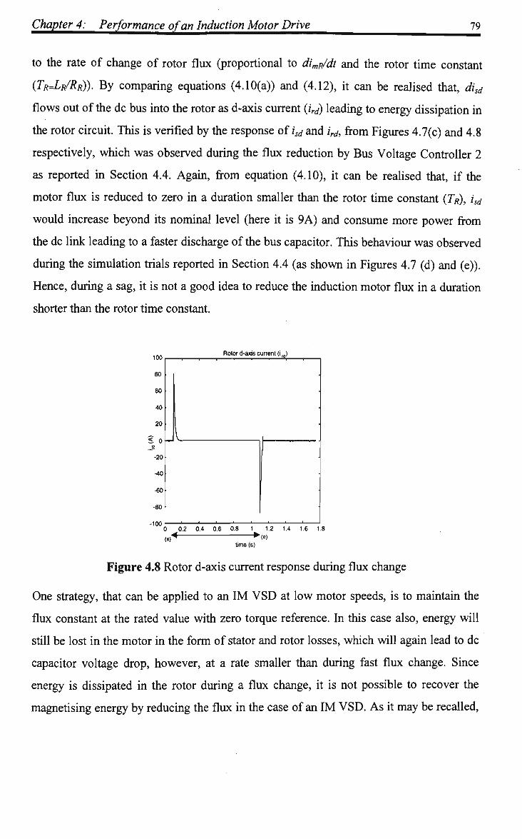
Chapter 4: Performance of an Induction Motor Drive 79
to the rate of change of rotor flux (proportional to dimR/dt and the rotor time constant
(TR=LR/RR)). By comparing equations (4.10(a)) and (4.12), it can be realised that, disd
flows out of the dc bus into the rotor as d-axis current (ird) leading to energy dissipation in
the rotor circuit. This is verified by the response of isj and ird, from Figures 4.7(c) and 4.8
respectively, which was observed during the flux reduction by Bus Voltage Controller 2
as reported in Section 4.4. Again, from equation (4.10), it can be realised that, if the
motor flux is reduced to zero in a duration smaller than the rotor time constant (7^), isd
would increase beyond its nominal level (here it is 9A) and consume more power from
the dc link leading to a faster discharge of the bus capacitor. This behaviour was observed
during the simulation trials reported in Section 4.4 (as shown in Figures 4.7 (d) and (e)).
Hence, during a sag, it is not a good idea to reduce the induction motor flux in a duration
shorter than the rotor time constant.
100
BO
60
40
20
< 0 ._? -20
-40
-60
-80
Rotor d-axis current (i M )
. \
I '
•
•
0 0.2 0.4 0.6 0.8 1 1.2 1.4 1.6 1.8
(s) time (s)
Figure 4.8 Rotor d-axis current response during flux change
One strategy, that can be applied to an I M V S D at low motor speeds, is to maintain the
flux constant at the rated value with zero torque reference. In this case also, energy will
still be lost in the motor in the form of stator and rotor losses, which will again lead to dc
capacitor voltage drop, however, at a rate smaller than during fast flux change. Since
energy is dissipated in the rotor during a flux change, it is not possible to recover the
magnetising energy by reducing the flux in the case of an I M V S D . As it may be recalled,
Chapter 4: Performance of an Induction Motor Drive 80
the intent of the proposed control strategy is to maintain the dc bus voltage constant at the
nominal level by recovering the magnetising energy, and this being not possible in the case
of an I M V S D , it must be ensured that the rate of decay of the capacitor voltage is as
small as possible for an extended sag ride-through performance. A n optimum dc bus
voltage control can be achieved by reducing the flux to zero in a duration marginally
longer than the rotor time constant and this can be achieved by an open loop flux control
scheme. The advantage of this control is that, the energy drawn from the dc bus capacitor
would not only be less than during constant flux control but would also continue to reduce
further. Hence, the dc bus voltage would reduce at a smaller rate which will enable the
V S D to ride-through sags of longer durations at low motor speeds down to zero speed.
Similar to d-axis currents, it can be found from equations (4.11) and (4.13) that, the stator
q-axis current (isq) flows into the rotor as q-axis current (irq) with a small percentage
impeded in the rotor leakage factor or.
4.6 OPTIMUM SAG RIDE-THROUGH CONTROL AT LOW SPEEDS
In this section, the behaviour of the VSD will be studied during a sag at low motor speeds
by reducing the flux to zero in a duration longer than the rotor time constant.
Simulation conditions: The same operating conditions as in the magnetising energy
recovery trials presented in Section 4.5 are maintained. Simulation results are shown for a
period of 2.05 seconds and a 1 second three-phase sag of 5 0 % magnitude is applied to the
VSD. During flux weakening, imR was reduced to zero in a duration corresponding to
twice the rotor time constant. O n normal ac supply recovery, the flux is increased at the
same slow rate in order to avoid high currents (isd). The normal speed control operation of
the V S D is restarted on supply recovery only when the motor flux becomes more than
97.5% of the rated value.

Chapter 4: Performance of an Induction Motor Drive 81
Motor speed (m) Magnetising current (i „.)
(e) time (s)
(a) Motor speed (co) Stator d-axis current (is„)
600
595
590
585
> 580
> 575
570
565
560
555
(e) time (s)
(c) stator d-axis current (isd) Capacitor Voltage (V,^)
- V„„„=586V \
0.5 1 1.5
"(•) time(s)
2.5
(e) time (s)
(b) Magnetising current (imR) Capacitor output current flj
(e) time (s)
(d) Capacitor current to inverter (hut) Capacitor charging current (J,)
60
50
40
< ws 3 0
20
10
n
' '
1
'
•
•
•
•
0.5 1.5
(e) time (s)
2.5
(e) Capacitor voltage (Vbus) (f) Capacitor charging current (/,„)
Figure 4.9 EVI V S D Response during slow recovery of magnetising energy

Chapter 4: Performance of an Induction Motor Drive 82
EVI VSD Response: The response of the IM VSD, viz. speed (co), magnetising current
(i„R), stator d-axis current (isd), capacitor output current to the inverter (lout), capacitor
voltage (Vbus) and the capacitor charging current (/,„), during this slow flux reduction
control are shown in Figures 4.9(a) to (f). The sag period is indicated as in the previous
trials and the duration of kinetic energy recovery and flux control are indicated as 'KE'
and ' M E ' respectively. From the magnetising current characteristics (refer Figure 3.9(b)),
it can be observed that the flux is reduced at a much smaller rate compared to the closed
loop flux control as shown in Figure 3.7(b). During this control, isd is also found to reduce
gradually and does not reverse its polarity (Figure 3.9(c)). Only a small amount of energy
is drawn from the dc capacitor corresponding to the reduced losses in the motor windings
which can be verified from the dc output current (hut) characteristics as shown in Figure
3.9(d). The capacitor voltage reduces at a much smaller rate during this control in a sag
condition and this results in reduced charging current at the instant of ac supply recovery
as found in Figures 3.9(e) and (f). W h e n the ac supply returns to normal, an overshoot is
observed in the capacitor voltage because the motor operates in regeneration mode until
zero speed is reached. This excess voltage occurs only in the case of loads such as hoists
or cranes and it can be discharged by the standard resistors available in the drive.
4.7 COORDINATED SAG RIDE-THROUGH CONTROL AT ALL SPEEDS
By combining the closed loop dc bus voltage control operation by recovering the kinetic
energy at higher speeds with the slow open loop flux control at lower speeds, the I M V S D
can be configured to ride-through voltage sags of longer durations at all operating speeds.
In this section, the V S D performance at a moderate speed is simulated such that the
coordinated transition between the two control modes is observed.
Simulation conditions: A 50% three-phase sag is applied to the EVI VSD operating at a
speed of 60 rad/s at half load (18Nm). Simulation results are shown for a period of 2.05
seconds. O n supply recovery, the V S D operation is restarted only when the flux reaches
97.5% of the rated value
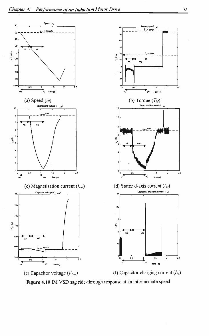
Chapter 4: Performance of an Induction Motor Drive 83
Speed (ra)
0
(s)
0.5 1
(«i
(a) Speed (<
1.5
time(s)
2>)
2 2.5
Magnetising current (i m C )
85G
800
~ 700
550
(c) Magnetisation current (imR) Capacitor voltage (V „.)
6501 <* »*« • XF ME
0 0.5 1 1.5 2 2.5
(») (e) time (s)
MotwtorqwfT .)
50
40
30
,-* 10
a
•10
•20
TLT-S4Nm
\ - 1BNm
KE ME
k •
0 0.5 1 15 2 25
•« »> (s) (•) tme(s)
(b) Torque (7^) Stator d-axis current (i ,„)
(e) time (s)
(d) Stator d-axis current (isd) Capacitor charging current (I J
time (s)
(e) Capacitor voltage (VbUs) (f) Capacitor charging current (/,„)
Figure 4.10 IM VSD sag ride-through response at an intermediate speed
Chapter 4: Performance of an Induction Motor Drive 84
EVI VSD Response: The response of the induction motor VSD, viz. the motor speed (co),
torque (TM), magnetisation current (imR), stator d-axis current (isd), capacitor voltage (Vbus)
and the capacitor charging current (/,„), during this combined sag ride-through operation
are shown in Figures 4.10(a) to (f). The sag period and the durations of kinetic energy
recovery and flux reduction control are indicated as previously. For motor speeds above
15.7 rad/s, the kinetic energy recovery is observed as shown in Section 4.2 earlier. The dc
voltage is maintained at the set value (586 V) . Once the cut off speed is reached, the
motor flux is found to reduce at a slower rate as observed from imR characteristics. The
capacitor voltage is found to reduce at a smaller rate because a very small current is drawn
by the motor in order to compensate the winding losses. W h e n normal ac supply returns,
the flux is found to increase at the same slower rate and isd is also found to increase
gradually without any high transients. The capacitor charging current (/,„) on ac supply
recovery is found to be within acceptable levels. A n overshoot is observed in the capacitor
voltage because the motor is regenerating until zero speed is reached.
4.8 SUMMARY
In this chapter, the normal behaviour of an IM VSD was demonstrated and its
performance when affected by a voltage sag was shown. It was observed that, in the case
of I M V S D s having a diode bridge rectifier, voltage sags affect the dc bus characteristics
and cause nuisance tripping due to dc under-voltage and ac over-current faults. The
performance of the proposed control strategy was studied on an EVI V S D and it was found
that, at high motor speeds, the dc bus voltage control by recovering the kinetic energy
from the rotating mass works satisfactorily. However, due to the inherent characteristics
of an EVI, it is found that, the magnetising energy present in the winding inductances
cannot be recovered and if flux is reduced to zero at a smaller duration than rotor time
constant, the I M draws excessive energy from the dc bus which is dissipated in the rotor
circuit. Here, a slow flux weakening scheme by an open loop control is proposed by which
the dc bus characteristics are found to have improved and this type of sag ride-through
control can be applied to an EVI V S D at low motor speeds.

85
CHAPTER 5
CONCLUSIONS
5.1 CONCLUSIONS
When considering the effects of power quality aspects in the industrial process
environment, voltage sags are found to be the primary source of concern causing nuisance
tripping of critical equipment such as Variable Speed Drives (VSDs). Nowadays, VSDs
are very commonly used in process plants and their tripping results in substantial financial
losses due to reasons such as wastage of raw materials, production downtime and
restarting delays. Hence, it is essential that the VSDs ride-through such sag situations to
the maximum possible extent. Several suggestions have been made in the literature which
are mostly hardware related solutions such as addition of extra circuitry, overrating the
existing components or provision of an alternative power supply. These solutions are
usually expensive and moreover they increase the size of the equipment. Very few of the
published strategies suggest solutions that would improve the control algorithm in a V S D
while retaining the standard hardware. This thesis was aimed at studying the behaviour of
VSDs during voltage sag conditions and to improve the ride-through performance by
modifying the control strategy.
Presently, ac VSDs with voltage source inverter (VSI) topology are the most commonly
used type of drives and hence this configuration was examined in this thesis with field
orientation applied to the motor control. Simulation models were developed and the
performances of synchronous reluctance motor VSDs (SRM VSDs) and induction motor
VSDs (IM VSDs) were examined under normal ac supply conditions as well as under sags
(of both three-phase and single-phase types). It was observed that the speed and torque
performance of both motors were not affected during most sag situations, except for a
minor speed drop observed during very deep three-phase sags. However, the main impact

Chapter 5: Conclusions 86
of the voltage sags was observed in the dc link (bus) characteristics of the VSDs. In the
case of a three-phase sag, the dc capacitor voltage reduces to a lower level, depending on
the magnitude of the sag, and when the ac supply returns to normal, a very high capacitor
charging current results. If left unprotected, the rectifier diodes would be damaged and
this situation usually results in V S D tripping due to either dc link under-voltage or ac
over-current protection faults which are built into the V S D control system in order to
protect the components. The probability of these trips increases with the sag magnitude
and load on the motor. In the case of a single-phase sag, the impact of the sag was found
to be less severe on the dc bus characteristics than a three-phase sag, due to the
intermittent capacitor charging by the unaffected phases. However, the voltage ripple and
the capacitor charging currents were found to increase with the sag magnitude. Though
the high recharging current peaks were not present at the end of a single-phase sag, V S D s
can still trip due to the faults mentioned earlier when subjected to sags of very high
magnitude, especially when operating under high load conditions.
The control strategy proposed in this thesis suggests maintaining the dc bus voltage at the
nominal level corresponding to the rated three-phase input supply conditions. From the
published literature, it can be found that this objective can be achieved by recovering the
kinetic energy available in the rotating mass by means of controlled regeneration. Since the
kinetic energy falls rapidly during regeneration in proportion to the square of the motor
speeds, this source can be utilised only until the motor speed is above a minimum limit. If
the sag condition persists even after the motor reaching zero speed, the bus voltage will
begin to drop leading to similar fault conditions, viz. under-voltage or over-current, as
mentioned earlier. The power supply for the control system is assumed to be derived from
the dc capacitor instead of ac mains which will buffer the effect of supply variations
affecting the control supply. The control strategy proposed in this thesis recommends
maintaining the dc capacitor voltage at the nominal value during a sag, initially by
recovering the kinetic energy available in the rotating mass when the motor speed is above
a minimum speed (here, the cut-off speed is chosen as 1 0 % of the rated motor speed) and
then by recovering the energy available in the motor winding inductances. Though the
Chapter 5: Conclusions 87
energy available in the inductances is relatively small compared to the energy present in the
capacitor under normal circumstances, the advantage of this strategy is that, it can be
applied at low speed and standstill. There will be no further losses in the motor apart from
the low voltage power supplies which will still draw power from the dc bus. Another
advantage of this strategy is that the voltage sag ride-through performance is not affected
by the type of the sag (three-phase or single-phase) or the sag magnitude because the
rectifier diodes are reverse biased during either type of sag and hence the dc link
characteristics are immune to the sag characteristics.
The performance of this proposed control strategy was studied on both SRMs and IMs of
similar ratings (5.5 k W ) . It was observed that the closed loop voltage control by
recovering the kinetic energy works satisfactorily with both types of machines. Longer sag
ride through times are achieved by this control mode when the motor speed is high and the
load on the motor is low. Hence this strategy is more suitable for high inertia loads. Better
ride-through performance with smaller speed drop was observed in the case of fan type
loads as compared to constant torque loads.
However the other part of the control strategy, viz. closed loop dc voltage control at low
motor speeds by recovering the energy available in the motor winding inductances, is
found to work satisfactorily only in the case of S R M V S D as envisaged by the control
strategy. It was observed that this energy is recovered within a few milliseconds but from
then on, the capacitor voltage remains close to the nominal value since there is no further
energy drawn from the dc link. W h e n the supply recovers to normal, the S R M V S D is able
to restart and reach the set speed without any abnormal capacitor charging current
transients.
When a closed loop dc bus voltage control was attempted on an IM VSD by recovering
the stored magnetic energy, it was observed that energy is drawn from the dc capacitor
rather than being fed back into it. W h e n analysed further, the reason for this behaviour was
found to be the inherent characteristics of the EVI, according to which, whenever the

Chapter 5: Conclusions 88
motor flux is changed, additional energy is drawn from the dc bus capacitor which is lost
in the rotor circuit. If the rotor flux is reduced to zero in a duration smaller than the rotor
time constant, the current drawn from the dc bus is more than the rated value which
reduces the dc link voltage at a rapid rate. Even when the motor flux is maintained
constant, energy is found to be lost in the stator and rotor circuits. Hence, the proposed
control strategy was modified to accommodate this limitation and an open loop flux
control scheme was examined which reduces the induction motor flux in a duration longer
than the rotor time constant. In this control, the energy drawn from the dc link and hence
the rate of dc bus voltage drop would be quite small. This strategy was found to work
reasonably well at low motor speeds and the capacitor recharging current at the end of the
sag was also found to be within acceptable limits.
In both types of motors, the transition between the two modes of the control strategy, viz.
recovery of energy from rotating mass as well as from the motor winding inductances, was
found to pass relatively easily between the appropriate control loops. The simulation
results of the combined control show that this strategy can be utilised to ride-through
voltage sags at all speeds.
According to the control strategy adopted in this thesis, as the input rectifier is not in
conduction during a sag, it effectively decouples the V S D load from the ac mains and
hence does not exacerbate the supply situation on the mains.

89
References
1) Puttgen, H.B., Rouaud, D., Wung, P., "Recent Power Quality Related Small to
Intermediate A S D Market Trends", P Q A '91, (First International Conference on
Power Quality: End-Use Applications and Perspective), Oct 15-18, 1991, Paris,
France.
2) Lipo, T., "Recent Progress in the Development of Solid-State AC Motor Drives",
IEEE Transactions on Power Electronics, v 3, n 2, April 1988, pp 105-117.
3) Huffrnann, H, "Introduction to Solid-State Adjustable Speed Drives", IEEE
Transactions on Industry Applications, v 26, n 4, July/August 1990, pp 671-678.
4) Sarmiento, H. G., Estrada, E., "A Voltage Sag Study in an Industry with
Adjustable Speed Drives", Industrial and Commercial Power Systems Technical
Conference, Irvine, CA, USA, May 1994, pp 85-89.
5) Dougherty, J.G., Stebbins, W.L., "Power Quality: A Utility and Industry
Perspective", Annual Textile, Fiber & Film Industry Technical Conference,
Greenville, SC, USA, May 1997, pp 1-10.
6) Gosbell, V.J., Perera, B.S.P., Doulai, P., "Power Quality Challenges and
Solutions", 1996, Presented at the Annual Conference of the Electricity Supply
Engineer's Association held at The Landmark Hotel, Sydney, 5th-7th August, 1996.
7) Collins Jr., E. R., Mansoor A., "Effects of Voltage Sags on AC Motor Drives",
1997 IEEE Annual Textile, Fiber and Film Industry Technical Conference
Greenville, SC, USA, May 1997; pp 1-7.
8) Mansoor, A, Collins Jr., E. R., Morgan, R. L., "Effects of Unsymmetrical voltage
sags on Adjustable Speed Drives", 7th Annual Conference on Harmonics and
Quality of Power, Las Vegas, N V , USA, October 1996, pp 467-472.

References 90
9) Scrangas, E. G , Wagner, V. E., Unruh, T. D., "Variable Speed Drives Evaluation
Test", IEEE Industry Applications Magazine, v 4, n 1, January/February 1998, pp
53-57.
10)Melhorn, C. J., "Voltage Sags: Their Impact on the Utility and Industrial
Customers", IEEE Transactions on Industry Applications, V 34, n 3, May/June
1998, pp 549-558.
11) Tang, L., Lamoree, J., McGranaghan, M., Mehta H, "Distribution System Voltage
Sags: Interaction with Motor and Drive Loads", IEEE Power Engineering Society
Transmission and Distribution Conference, Chicago, DL, USA, April 1994, pp 1-6.
12) Power System Reliability Subcommittee Voltage Sag Working Group, "Proposed
Chapter 9 for Predicting Voltage Sags (Dips) in Revision to IEEE Std 493, the
Gold Book ', Industrial and Commercial Power Systems Technical Conference,
St.Petersburg, FL, USA, May 1993, pp 43-51.
13)Bollen, M.H.J., "Characterisation of Voltage Sags Experienced by Three-Phase
Adjustable Speed Drives", EEEE Transactions on Power Delivery, v 12, n 4,
October 1997, pp 1666-1671.
14)Bollen, M.H.J., Zhang, L., "A Method for Characterisation of Three-Phase
Unbalanced Dips from Distorted Voltage Waveshapes", Unpublished Paper,
February, 1999.
15)Vas, P., Drury, W., "Electrical Machines and Drives: Present and Future",
Industrial applications in Power Systems, Computer Science and
Telecommunications, Bari, Italy, v 1, May 1996, pp 67-74.
16) David, A, Lajoie-Mazenc, E., "Maintaining the Synchronism of an AC Adjustable
Speed Drive during Short Supply Interruptions for an Optimal and Automatic Soft
Restart", IEEE International Symposium on Industrial Electronics, June 1-3, 1993,
Budapest, Hungary, (Cat. No. 93TH0540-5) pp 463-470.
References 91
17)Tichenor, J.L., Sudhoff, S.D., Brownfield, G , Scheppers, D., "Tripping of
Adjustable Speed Drives Due to Brief Voltage Reductions", IEEE International
Electric Machines and Drives Conference, Milwaukee, WI, USA, May 1997.
18) Sisa, E. M., "Power Outages and Power Dip Ride-Through", IEEE Annual Textile,
Fiber and Film Industry Technical Conference (Cat. No. 95CH3580-6), Chorlette,
NC , USA, May 1995.
19) David, A., Lajoie-Mazenc, E., Sol, C, "Ride through Capability of AC Adjustable
Speed Drives in regards to Voltage Dips on the Distribution Network" 5th
European Conference on Power Electronics and Applications, Brighton, UK,
September 1993, v 6, n 377, pp 139-144.
20)Duran-Gomez, J.L., Enjeti, P., "A Low Cost Approach to Improve the
performance of an Adjustable Speed Drive (ASD) under Voltage Sags and Short-
Term Power Interruptions", IEEE Applied Power Electronics Conference and
Exposition - APEC. v 2, Anaheim, CA, USA, February 1998, pp 587-591.
21)Zyl, A. V., Spee, R, Faveluke, A, Bhowmik, S., "Voltage Sag Ride-Through for
Adjustable Speed Drives with Active Rectifiers", IEEE Industrial Applications
Society Annual Meeting, N e w Orleans, Louisiana, October 5-9, 1997, pp 486-492.
22) Chattopadhyay, S., Key, T. S., "Predicting Behaviour of Induction Motors During
Electrical Service Faults and Momentary Voltage Interruptions", IEEE Industrial
and Commercial Power Systems Technical Conference (Cat. No.93CH3255-7). pp
78-84.
23) Tan, O. T., Paap, G. C , Kolluru, M. S., "Thyristor-Controlled Voltage Regulators
for Critical Induction Motor Loads During Voltage Disturbances", IEEE
Transactions on Energy Conversion, v 8, n 1, March 1993, pp 100-106.
References 92
24) David, A., Lajoie-Mazenc, E., Sol, C , "Soft Restart of an Adjustable Speed Drive
After a Short Disconnection Without Any Mechanical Speed Sensor", IEE
International Conference on Electrical Machines And Drives, Oxford, UK, Sept.
93, pp 570-575.
25)Holtz, J., Lotzkat W., "Controlled AC Drives with Ride-Through Capability at
Power Interruption", Industrial Applications Society Annual Meeting, Toronto,
Ontario, Can., v 1, October 1993, pp 629-636.
26)Leonhard, W., "Control of Electric Drives", Springer, 1996.
27) Vas, P., "Vector Control of AC Machines", Oxford Science Publications, 1990.
28)Bose, B.K., "Microcomputer Control of Power Electronics and Drives", IEEE
Press, 1987.
29)Boldea, I, Nasar S.A., "Vector Control of AC Drives", CRC Press Inc., 1992.
30) Zhang, L., Hardan, F., "Vector Controlled VSI-Fed AC Drive Using A Predictive
Space Vector Current Regulation Scheme", International Conference on Industrial
Electronics, Control and Instrumentation, Bologna, Italy, September 1994, pp 61-
66.
31)Mathew, R., Houghton, D., Oghanna, W., "Vector Control Techniques For
Induction Motors", International Conference on Power Electronics and Drive
Systems, Singapore, v 2, February 1995, pp 813-818.
32) Chin, T.H., "Approaches for Vector Control of Induction Motor Without Speed
Sensor", International Conference on Industrial Electronics, Control and
Instrumentation, Bologna, Italy, September 1994, pp 1616-1620.
References 93
33)Wade, S., Dunnigan, M. W., Williams, B.W., "Modelling and Simulation of
Induction Machine Vector Control with Rotor Resistance Identification", IEEE
Transactions on Power Electronics, v 12, n 3, May 1997, pp 495-506.
34)Casadie, D., Gradi, G., Serra, G, "Rotor Flux Oriented Torque-Control of
Induction Machines Based On Stator Flux Control", 5th European Conference on
Power Electronics and Applications, Brighton, UK, v 5, n 377, September 1993,
pp 67-72.
35)Hughes, A., Corda, J., Andrade, D. A, "Vector Control of Cage Induction
Motors: A Physical Insight", EEE Proceedings on Electric Power Applications, v
143, n 1, January 1996, pp 59-68.

94
APPENDIX A
ENERGY LEVELS IN AN AC VSD
Here, an overview of the energy levels present in an induction motor VSD (EVI VSD).
of rating 5.5 kW is presented. These values are also applicable for a synchronous
reluctance motor VSD (SRM VSD).
Energy in motor winding inductance (D:
Assuming a star connected motor,
415 1 p.u. volts = —j=r = 240 V rms (A. 1)
Considering a power factor of 0.85,
5500 1 p. u. current = - p : — = 9 A (A.2) v V3*415*0.85
240 Hence, 1 p.u. impedance, Z = = 26.67 Q (A3)
Let us assume Xh&tXt = coLt = 2.5 p.u. Z = 66.675 CI (A.4)
where,
Xt - total reactance of the ac machine
L, - total inductance of the ac machine
66675 Then, Lt = = 212 m H (A.5)
1 2/r50
9*V2 Peak current in Lt - = 5.09 A /^
At the same time, current in other phases = -2.55 A
Hence, energy stored inLt = -L (5.092 +2.552 +2.552) = 4.12 J (A.7)
Appendix A: Energy Levels in an AC VSD 95
Energy in Motor Inertia (J)* i.e. kinetic energy:
120*/ Rated speed of the motor = = 157 rad/s (A. 8)
P
where,
/- supply frequency,
p - number of poles in the motor
1 2
Energy present in the rotating mass at rated speed =—Jco =2834.6 J (A. 9)
where,
J- Moment of inertia (in this case, 0.23 kgm2)
The kinetic energy varies proportional to the square of the motor speed.
Energy in dc Bus Capacitor (Q:
With 415 V, 3 phase AC supply,
dc voltage = 415*V2 = 587V (A. 10)
Rated dc current at full load of the motor = = 9.37 A (A. 11) 587
Let us assume that the bus capacitance C is chosen for 5 % ripple
C = / — = — = 1064 uF * 1000 pF dV 50*6*587*0.05 (A. 12)
1 ~ Energy stored in the capacitor = -CV1 = 172.28 J (A. 13)
If we do not require the capacitor to reduce the 300 Hz ripple in the ac supply
frequency, it will nevertheless have to be large enough to keep switching frequency
ripple to, say 5%. If the switching frequency of each of the six IGBTs is 5 kHz, then a
switching event takes place at an average interval of — - — j = 33.33 ps.
Appendix A: Energy Levels in an AC VSD 96
In this case,
C = i— = — — =10.64 pF*\OpF dV 30 *10 3* 587* 0.05
1 2
Energy stored in the capacitor = — CV = 1.72 J
It can be seen that there is considerable amount of energy available in the motor
inductances and the rotating mass as compared to the energy levels present in the bus
capacitor. These sources of energy shall be utilised in order to maintain the dc bus
voltage at a required level during a voltage sag.
(A 14)
(A. 15)
97
APPENDK B
MATHEMATICAL MODELLING OF AN INDUCTION MOTOR
Field orientation control modelling of cage induction motors [EVI] is discussed in [26-
35]. The basic equations of the EVI, viz. the equations corresponding to the stator
voltage, rotor voltage, torque and speed, whose derivations are presented in [26] are
as follows:
dt "dt
2 TM=-Lm-ba L(le") (B.3)
de - = » (B.5)
where,
Rs, Rr - stator and rotor resistances
Ls, Lr - stator and rotor inductances
Lm - mutual inductance
£ - rotor position
co - rotor angular velocity
is, ir- stator and rotor current vectors
TM, TL - motor and load torques
J- moment of inertia of the rotating mass
It can be seen from the motor torque equation (B.3) that, the motor generates a torque
(TM) based on the interaction between the rotor and stator current vectors. Since, rotor
currents are not measurable in the case of squirrel cage motors, it should be replaced
by an equivalent measurable quantity. The best alternative is the magnetising current

Appendix B: Mathematical Modelling of an Induction Motor 98
vector (imR) which is defined in equation (B.6) in terms of the stator coordinates [26]
The stator current vector (Ts) is defined by equation (B.7) which is seen as moving
with respect to the flux axis. The angular relationships of the moving current vectors
are shown in Figure B.l.
'*=in*eJp =7,+Q + <rr)rre
le~JP=isejS=isd+jisq
where,
i^ - magnetising current vector
imR - magnetising current
p - magnetising (flux) axis position with respect to stator axis
or - rotor leakage factor
8 - load angle
isd, isq - stator currents in d and q axes
1 y
V'-1 ^ *>* --
<°1/
\*3£ • — j f z ^
'.
"C TP
.
sq
Rotor axis
.,-'3i" < B m R w _ _ Magnetising
— — *" li ' axis
Stator axis
(B.6)
(B.7)
Figure B.l Angular relationships of stator current vectors in an I M in steady state [26]
Based on equation (B.7), w e get
iSd = R e p > - 'p ] = /,cos<5
isq =Im[/>"; p] = /ssin£
(B.8)
(B.9)
Hence, in Figure B.l, iid is found to align with the magnetisation axis and isq is
perpendicular to it.

Appendix B: Mathematical Modelling of an Induction Motor 99
By replacing 7reJE from equation (B.6) in the torque equation (B.3), we get
But, from equation (B.6),
'mR 'mRc
Hence, equation (BIO) becomes,
T^^-^i^ImTiy''] (B.ll) 3 l + CTr
L J
By substituting equation (B.9), equation (B. 11) becomes,
^ = * W , (B.12)
where,
2 I. £ =
31 + o\
Here, /^ is the magnetising current and is controlled by the stator d-axis current isd
whereas the q-axis current isq is the torque producing component. Hence, isd and isq are
the two independent quantities that control the flux and torque of the IM. Here, the
flux axis, which is defined by the orientation of the magnetising current vector i^,
forms the frame of reference and it rotates across the stator axis at the stator frequency
and across the rotor at the slip frequency [26].
Stator currents:
By substituting equation (B.6) into rotor voltage equation (B.2) and re-organising the
real and imaginary terms, the equations representing the stator currents in field
coordinates are derived as follows:
% = «.*=« + - CB.14) at iR imR
or isq = (amR ~(o)TRimR (B.l4a)

Appendix B: Mathematical Modelling of an Induction Motor 100
where,
co - rotor angular velocity
cOmR - angular velocity of the magnetisation axis
From equation (B.l3), it can be observed that the rotor flux (imR) lags isd by a delay
equivalent to rotor time constant (Tr).
Stator voltages (Vsd and Vsq):
The stator voltages in field coordinates for an IM are derived from the stator voltage
equation as shown below:
The stator voltage equation is
R/t+LgiL+Lm±(Tre») = VM ss s dt m dtKr } s
By substituting for TreJ£from equation (B.6), equation (B.l) becomes,
Lm(l + os) d (7 - dis Rsis + As —~ + dt (1 + o-j) (l + crr) dt
Since, stator inductance Ls = Lm(\ + os) and
1
-r(imR-is) = Vs
total leakage factor o = 1 -
equation (B. 15) becomes,
(l + o,)(l + or)
Rsis+Lso^ + (^-^Ls^ = Vs
From equation (B.7), the stator current vector can be represented as
lsq. fs = (isd + isq) eJP
Hence, - = ejP dt
di sd ^
COmD h.r -jf-VmR'sq + j di sq dt + tomR isd
where.
comP = speed of the flux axis "* dt v
(B.l)
(B.l 5)
(B.l 6)
(B.l 7)

Appendix B: Mathematical Modelling of an Induction Motor 101
Also from equation (B.6), w e know that the magnetising current vector
imR - imR e JP
Hence,
di T&. _ eJP dt
di mR dt
+ J <°mR imR
The stator voltage vector can be represented as:
Vs = {Vsd+JVsq)eJP
(B.l 8)
(B.19)
By substituting equations (B.l7) to (B.19) into equation (B.16) and by equating the
real and imaginary components, we get:
Vsd = Rsisd +oLs(^f-comRiscl) + (\-o)LsdlmR
-0—VmR'sq. dt
di £4 dt Vsq = Rs isq + 0"4(-7r + <°mR isd) + (1 ~ O") 0>mR
jmR
(B.20)
(B.21)
Rotor currents:
The orientation of rotor current vector Trin the magnetising frame of reference is
shown in Figure B.2.
a v . Rotor axis
comR w _ Magnetising — — " j " " axis
Stator axis
Figure B.2. Angular relationships of rotor current vectors in steady-state in an IM
By transforming the coordinates of the rotor current vector with respect to the
magnetising axis, we get:

Appendix B: Mathematical Modelling of<*n Induction Motor 102
Replacing Tr from rotor equation (B.2) utilising equation (B.6),
Rjr + Lme-» 4*- - jcoLJ^* = 0
Substituting equations (B.6), (B18) and (B.22) into equation (B.23),
ird +Jirq = (di mR \ dt
+ JG>mRimR\-J<»LJ, mR
(B.23)
(B.24)
By equating the real and imaginary components from above equation, the rotor
currents are obtained as follows:
'rd KdimR Rr dt
(B.25)
(B.26)
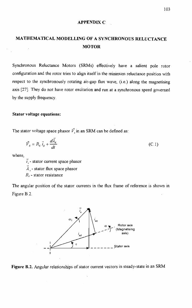
103
APPENDIX C
MATHEMATICAL MODELLING OF A SYNCHRONOUS RELUCTANCE
MOTOR
Synchronous Reluctance Motors (SRMs) effectively have a salient pole rotor
configuration and the rotor tries to align itself in the minimum reluctance position with
respect to the synchronously rotating air-gap flux wave, (i.e.) along the magnetising
axis [27]. They do not have rotor excitation and run at a synchronous speed governed
by the supply frequency.
Stator voltage equations:
The stator voltage space phasor Vs in an S R M can be defined as:
dAQ V. = *.!. + =£ (C.l)
where,
is - stator current space phasor
Xs- stator flux space phasor
Rs - stator resistance
The angular position of the stator currents in the flux frame of reference is shown in
Figure B.2.
co ». _ Rotor axis ___ -n" (Magnetising
axis)
Stator axis
Figure B.2. Angular relationships of stator current vectors in steady-state in an S R M

Appendix C: Mathematical Modelling Of A Synchronous Reluctance Motor 104
In the rotor (magnetising) frame of reference, the stator current, voltage and flux space
phasors can be represented as:
l^(isd+jisq)ej£ (C.2)
Vs=(Vsd+jVsqys (c.3)
* , = ( * - + * „ * ' * (C.4)
where,
e - rotor position with respect to stationary reference frame
isd, isq - stator currents in d and q axes
Vsd, Vsq - stator voltages in d and q axes
Kd, Kq - stator flux linkages in d and q axes
Substituting equations (C.2) to (C.4) in (C. 1), w e get:
d_
dt (Vsd +JVaqy = Rs(isd +jisq)e
je +%-(*« +&«)**
d (C.7)
;* = Rs('sd +Jisqyie +J<»(Asd +MSq)e
Je+-^Vsd +*Sq)e
The d and q axis flux linkages can be expressed in terms stator currents [29] as:
K = Usd (C5)
*sq = Kqisq (C6)
Replacing ksd and Xsq in equation (C.7) from equations (C.5) and (C.6), w e get:
di A set
Vsd + jVsq = Rs(isd+jisq ) + j(oLsdisd - coLsqisq + Lsd -±- + jLsq — (C. 8)
By equating the real and imaginary terms in equation (C.8), the stator voltage
equations in field coordinates are obtained as follows:
Vsd=RJsd-<oLsqisq+Lsd^- (C.9)
V^Rj^aLJt+L^ (CIO)

Appendix C: Mathematical Modelling Of A Synchronous Reluctance Motor 105
Torque and speed equations:
The S R M torque and speed equations are:
TM=^Npp(Lsd-Lsq)iJsq (CM)
(C.12)
(C.13)
where,
T
CO =
Npp
7A/-
Ti-
Kd,
~TL
ds
dt
= Jdco_
dt
- number of pole pairs
- motor torque
load
Ajgr —
torque
stator flux linkages in d and q axes

106
Appendix D
Switching Vector Selection
Here, the switching sequence of the voltage source inverter when controlled by field
orientation technique (vector control) is analysed.
The P W M inverter, which is employed in the V S D configuration chosen in this thesis,
has 6 switches, with two of them on each of the three inverter poles (legs). The
inverter supplies power to the ac motor by connecting the three motor terminals to
either the positive or negative terminal of the dc bus. A simplified representation of a
three-phase voltage source inverter circuit is shown in Figure D. 1.
J To ac motor
Figure D.l. A three-phase inverter
Both switches on a pole must not be turned on at the same time, in order to avoid
short circuiting of the dc supply. Similarly, both switches in a leg must not be opened
at the same time. The control system must ensure that each phase of the ac motor is
connected to either the positive or the negative terminal of the dc bus.
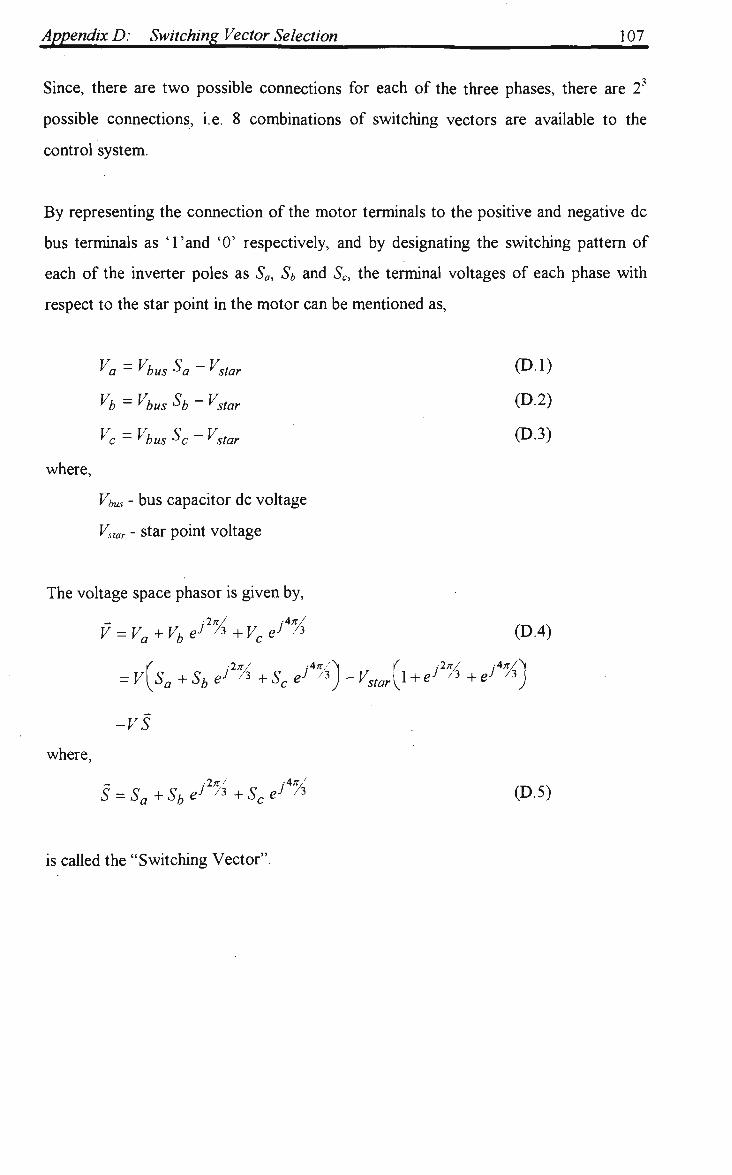
Appendix D: Switching Vector Selection 107
Since, there are two possible connections for each of the three phases, there are 23
possible connections, i.e. 8 combinations of switching vectors are available to the
control system.
By representing the connection of the motor terminals to the positive and negative dc
bus terminals as T a n d '0' respectively, and by designating the switching pattern of
each of the inverter poles as Sa, Sb and Sc, the terminal voltages of each phase with
respect to the star point in the motor can be mentioned as,
Va=VbusSa-Vstar (DI)
Vb = Vbus Sb - Vstar (D.2)
Vc=VbusSc-Vstar (D.3)
where,
Vbus - bus capacitor dc voltage
Vstar - star point voltage
V = Vn + Vh eJ /3 + Vr e
J A (D.4)
The voltage space phasor is given by,
= v(Sa+ Sb e'2'A + Sc SK) - Vslar{, + e^ + e^)
=VS
where.
S = S„+SheJ2^+SreJ
4*/i (D.5)
is called the "Switching Vector".

Appendix D: Switching Vector Selection IQS
For the 8 possible combinations of S (Sa Sb Sc), the values of S and V in the real and
imaginary coordinates and their angle with respect to the real axis are,
Sa Sb Sc Ke{S) lm(S) Re(V) Im(f) Angle
000 0 0 0 0
001 ~\ -JY ~\vbus ~JYVbus 240°
010 ~\ J~l -\Vbus JYVbus 120°
o 011 -1 0 -Vbus 0 180
100 1 0 Vbus 0 0°
1 A iv -^ 2 J 7 9 *bus J ,
1 A \v ^ 2 J 2 2 bus J 2 0 0 0 0
101 2 -7-J- 2Vbus ~JYVbus 3°°C
110 ^ J~Y 2Vbus J^Vbus 60°
Two of the switching vectors, viz. 000 and 111, are zero vectors and the other six
outer vectors are unit vectors on the complex plane and they are called the "active
vectors".
The position of the switching vectors on the complex plane are shown in Figure D.2.
011
001 101
Figure D.2. Switching vectors in the complex plane
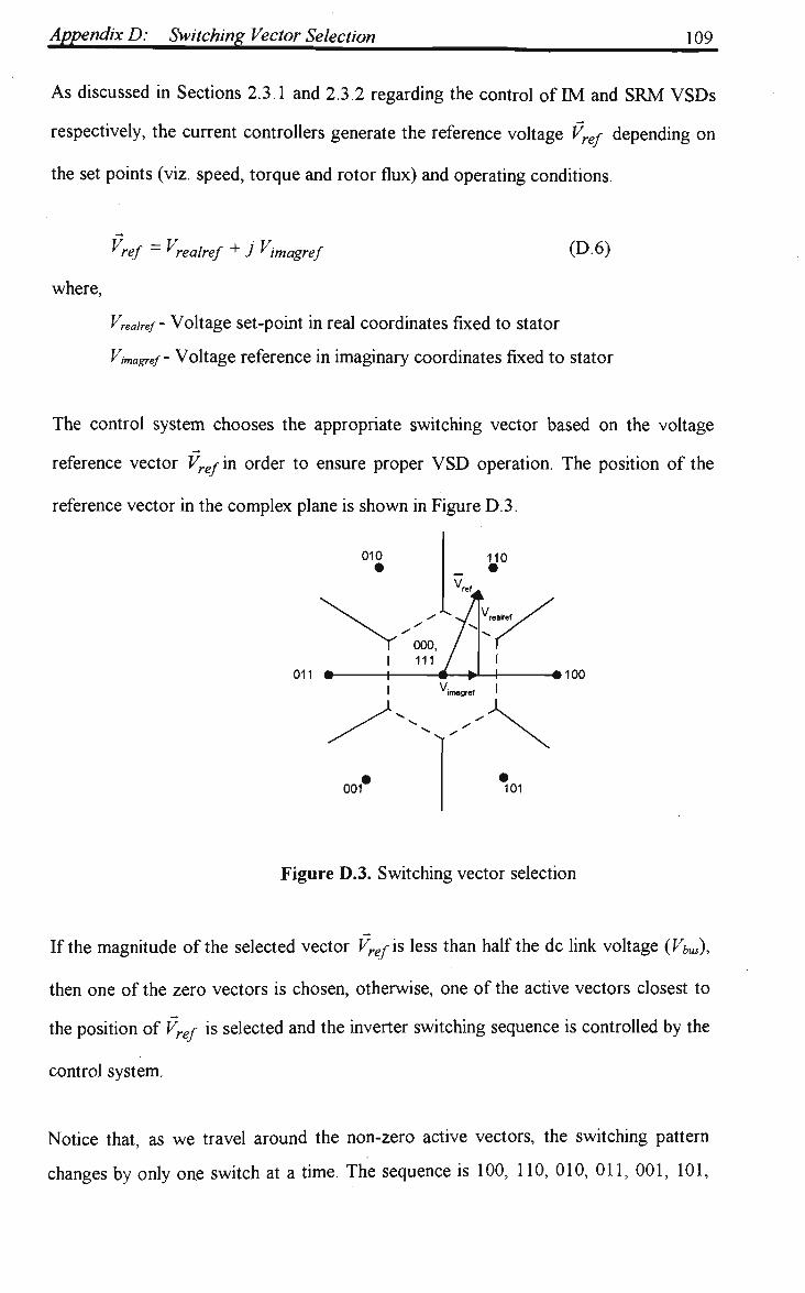
Appendix D: Switching Vector Selection 109
As discussed in Sections 2.3.1 and 2.3.2 regarding the control of EVI and S R M V S D s
respectively, the current controllers generate the reference voltage Vref depending on
the set points (viz. speed, torque and rotor flux) and operating conditions.
"ref ~ "realref + J 'imagref (D.6)
where,
Vreairef- Voltage set-point in real coordinates fixed to stator
Vmagref- Voltage reference in imaginary coordinates fixed to stator
The control system chooses the appropriate switching vector based on the voltage
reference vector Vrej in order to ensure proper V S D operation. The position of the
reference vector in the complex plane is shown in Figure D.3.
011 • 100
Figure D.3. Switching vector selection
If the magnitude of the selected vector Krgyis less than half the dc link voltage (Vbus),
then one of the zero vectors is chosen, otherwise, one of the active vectors closest to
the position of Vref is selected and the inverter switching sequence is controlled by the
control system.
Notice that, as we travel around the non-zero active vectors, the switching pattern
changes by only one switch at a time. The sequence is 100, 110, 010, Oil, 001, 101,

Appendix D: Switching Vector Selection 110
100). Also, to move from any of these vectors to a zero vector, only one switch needs
to be changed, since either of the two zero vectors (000 or 111) can be chosen. So, to
select a neighbouring vector, only one pair of switches in an inverter pole need to be
changed. However, to move from one non-zero vector to another by two steps, two
pairs of switches need to be changed. To move to the directly opposite vector, we
need to change all the inverter switches. Therefore, the switching frequency can be
kept to a minimum by limiting the choice of voltage vectors as below:
a) If the present vector is one of the outer active vectors, only the two immediate
neighbours or a zero vector may be chosen.
b) If the present vector is one of the zero vectors, only the 3 active vectors require
only one switching transition, can be selected, (i.e. from 000, only 100, 010 or 001
can be chosen. Similarly from 111, only 110, 011 or 101 can be chosen).
The movement from one voltage vector to another requires one switch in a pole be
turned O N while the other turned OFF. If in 1 second there are N vector transitions,
N N . then on the average, each switch will turn O N —times and turn OFF —times. Hence,
6 6 N
the average switching frequency will be — .

I l l
A P PENDIX E
PARAMETERS OF INDUCTION MOTOR VSD (EVI VSD)
Motor Parameters:
Power Rating - 5.5 k W
Input supply conditions - 415 V AC, 3ph, 50 Hz
Rated speed (co) - 1500 rpm (157 rad/s)
Rated torque (7^) - 36 N m
Number of pole pairs (Npp) - 2
Stator resistance (Rs) - 0.673 CI
Rotor resistance (Rr) - 1.2964 CI
Mutual Inductance (Lm) - 0.2925 H
Stator Leakage factor (os) - 0.0484
Rotor Leakage factor (or) - 0.0484
Moment of inertia (J) - 0.23 Kg m 2
VSD Parameters/Settings:
Torque Limit (TLT) - 54 N m
Bus capacitor (Q - 1000 uF
Speed controller proportional gain (Kp,sp) -148
Speed controller integral gain (KUsp) - 31671
Magnetising current ref. (imRref) - 9 A
Minimum limit of imR (imRmm) - 0 A
Maximum limit of isd (isdmax) - 9 A
Minimum limit of isd (isdmm) - 0 A
Cut-off speed for control transition ( G W # ) - 15.7 rad/s
Bus Voltage Regulator 1 proportional gain (Kp,bi) - 2.68
Bus Voltage Regulator 1 integral gain (Kubf) - 573.75
Bus Voltage Regulator 2 proportional gain (KPtb2) - 0.3585
Bus Voltage Regulator 2 integral gain (Kj^) - 128.45

Appendix E: Parameters of Induction Motor VSD 112
Simulation parameters:
Per-phase line resistance (Ra) - 0.0085 Q
Per-phase line inductance (La) -0.1 m H
IGBT Switching frequency - 5 kHz
Sampling time (dt) - 33 |is
Velocity reference (coref) - 0 to 157 rad/s
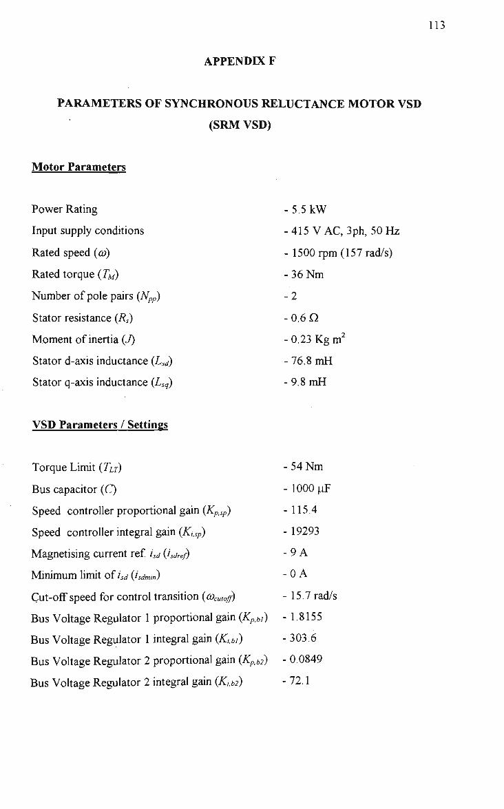
APPENDLY F
PARAMETERS OF SYNCHRONOUS RELUCTANCE MOTOR VSD
(SRM VSD)
Motor Parameters
Power Rating - 5.5 kW
Input supply conditions - 415 V AC, 3ph, 50 H z
Rated speed (co) - 1500 rpm (157 rad/s)
Rated torque (TM) - 36 N m
Number of pole pairs (NPP) - 2
Stator resistance (Rs) - 0.6 Q
Moment of inertia (J) - 0.23 K g m 2
Stator d-axis inductance (Lsd) - 76.8 m H
Stator q-axis inductance (Lsg) - 9.8 m H
VSD Parameters / Settings
Torque Limit (TLT) - 54 Nm
Bus capacitor ( Q - 1000 uF
Speed controller proportional gain (KPfSp) - 115.4
Speed controller integral gain (Ki.sp) -19293
Magnetising current ref. isd (isdref) - 9 A
Minimum limit of isd(isdmw) - 0 A
Cut-off speed for control transition (cocutoff) -15.7 rad/s
Bus Voltage Regulator 1 proportional gain (Kp,bi) -1.8155
Bus Voltage Regulator 1 integral gain ( K M ) - 303.6
Bus Voltage Regulator 2 proportional gain (Kp,b2) - 0.0849
Bus Voltage Regulator 2 integral gain ( K M ) - 72.1
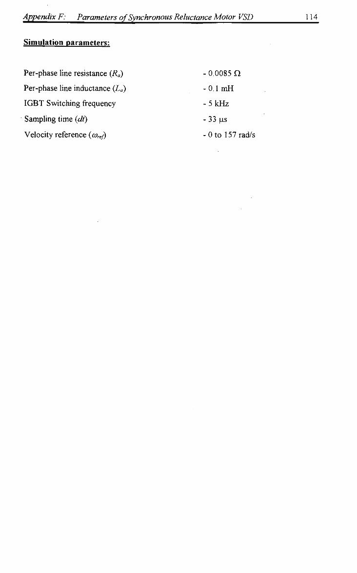
Appendix F: Parameters of Synchronous Reluctance Motor VSD 114
Simulation parameters:
Per-phase line resistance (Ra) - 0.0085 Cl
Per-phase line inductance (La) - 0.1 m H
IGBT Switching frequency - 5 kHz
Sampling time (dt) - 33 (is
Velocity reference (coref) - 0 to 157 rad/s

115
APPENDED G
TUNING OF CONTROLLERS FOR INDUCTION MOTOR VSD (EVI VSD)
(a) Speed Controller
The simplified block diagram of the speed control loop of an EVI VSD is shown in
Figure G. 1. Only full flux operation is considered in this thesis and field weakening is
not considered.
- ^ • 6 * -2
to
i ^
Speed controler
• 1
PP 1W " ^
1
1+V
Current controler
• NW*U ±+&+ 1
Js
to
— • 1
s
Figure G.l. Speed control loop block diagram of an I M V S D
It can be observed that, the above control block diagram shown in Fig. G. 1. represents
the functional behaviour of the I M V S D during speed control which is described in
Subsection 2.3.1. The speed regulator, which is a proportional-integral (PI) controller,
generates a torque reference (Tref) based on the speed error, which is converted into a
current reference (isqref) based on motor torque equation (G.l). The closed loop
1 operation of the current controller is modelled by the transfer function
i+V [26],
where the time constant Tsq is the time taken for 1 0 0 % change in the torque producing
current isq by applying the rated dc voltage Vbus and assuming that half the rated
voltage is already available in the motor as back emf. The calculation of Tsq is shown
by equation (G.2). The motor torque, speed and position calculations are based on
equations (G.l), (G.3) and (G.4).
TM = NppKimRisq (G.l)
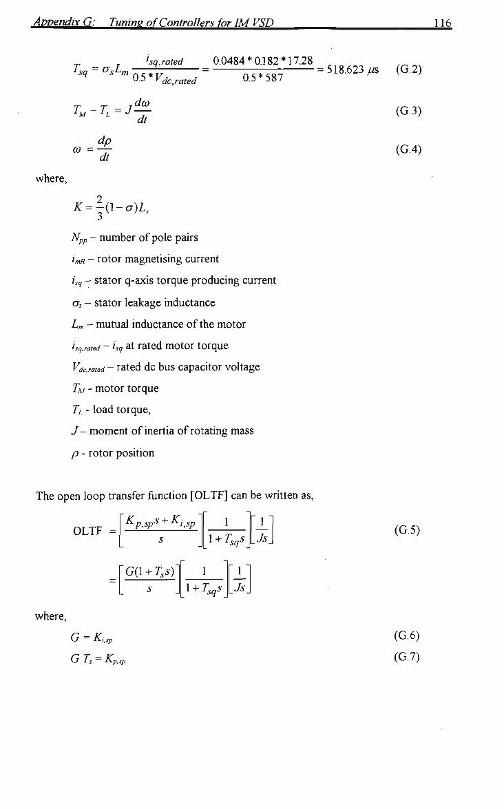
Appendix G: Tunint? of Controllers for IM VSD 116
*sq us^m
lsq,rated
0 5 * Vdcsated
0.0484*0.182*17.28
0.5*587 = 518.623 ps
T - T - T^SL M L~ dt
CO = dp
dt
where,
K = -(l-o)Ls
Npp - number of pole pairs
imR ~ rotor magnetising current
isq - stator q-axis torque producing current
os - stator leakage inductance
Lm - mutual inductance of the motor
isq.rated - iSq at rated motor torque
Vderated - rated dc bus capacitor voltage
TM - motor torque
TL - load torque,
J- moment of inertia of rotating mass
p - rotor position
(G.2)
(G.3)
(G.4)
The open loop transfer function [OLTF] can be written as,
where,
OLTF = ^p,sps "*" i,sp
S
\G(\ + Tss)~\
s
1
\ + Tsqs_
1
} + TsqS_
' 1"
Js_
~ 1
_Js
G — Ki,sp
GTS = KP, W
(G.5)
(G.6)
(G.7)

Appendix G: Tuning of Controllers for IM VSD 117
The bode plot of the open loop gain has a slope of -40 db/decade except between the
two corner frequencies. The controller corner frequency is chosen such that the slope
in this interval is -20 db/decade.
The controller gains G and Ts can be chosen such that the zero db point, i.e. cross-over
frequency cocr0ss, is in the centre of the section with -20 db/decade slope. This gives the
maximum phase margin (which is 53°).
-40 db/ decade
Odb co
Figure G.2. Bode plot of the speed loop
In terms of the corner frequency, the optimum values of Ts and coCToss are [26],
T T 1sq
1s
3 to cross ~ -r
1s
1 1
~ 3Tsq ~3*518.623*10~6 = 642.72 rad / s
(G.8)
(G.9)
At co.
i.e.
OLTF =1
G\l + .p\
1 1 + J3
~3T 3T J1sq
J1sq J
= 1 (G.10)
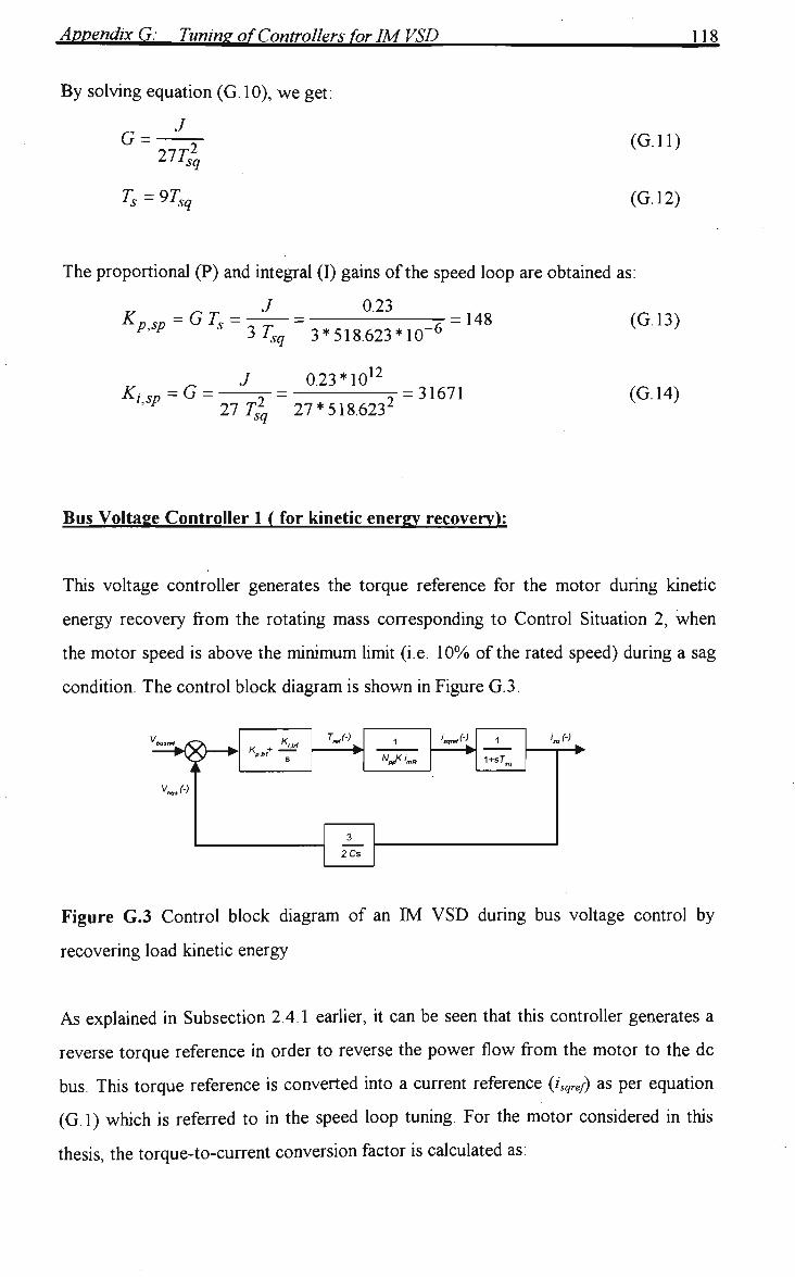
Appendix G: Tunine of Controllers for IM VSD
By solving equation (G. 10), we get:
J G =
277; sq
T =9T 2s ^xsq
(G.ll)
(G.12)
The proportional (P) and integral (I) gains of the speed loop are obtained as:
J 0.23 - p,sp ^ -*s ~
Ki,sp -G-
lTsq 3* 518.623 *10~6
J 0.23 *1012
= 148
,sp 27 T?q 27*518.6232 = 31671
(G.13)
(G.14)
Bus Voltage Controller 1 ( for kinetic energy recovery):
This voltage controller generates the torque reference for the motor during kinetic
energy recovery from the rotating mass corresponding to Control Situation 2, when
the motor speed is above the minimum limit (i.e. 1 0% of the rated speed) during a sag
condition. The control block diagram is shown in Figure G.3.
•=H8)—*
V.U.U
*«(->
W.
U « 1
1+sT
'-«
3
2Cs
Figure G.3 Control block diagram of an IM V S D during bus voltage control by
recovering load kinetic energy
As explained in Subsection 2.4.1 earlier, it can be seen that this controller generates a
reverse torque reference in order to reverse the power flow from the motor to the dc
bus. This torque reference is converted into a current reference (4^/) as per equation
(G.l) which is referred to in the speed loop tuning. For the motor considered in this
thesis, the torque-to-current conversion factor is calculated as:

N^Ki^ 2*0.1157*9 = 0.48 (G.l 5)
where,
K = -(\-o)Ls= -(1-0.090199)* 0.1908 = 0.1157
imR - rated magnetising current = 9A
The closed loop current controller is once again modelled by the transfer function
1
1 + Tsqs similar to the speed loop tuning. In this control, the magnetising current imR
(and hence isd) is maintained at the rated value and the reversal of isq reverses the flow
of the current (/„„,) from the motor to the capacitor (C) which results in the increase of
the capacitor bus voltage Vbus according to equation (G.l6). Assuming that, the
product Vsdisd is constant and Vsq applied is equivalent to Vbus, the relationship between
iSq and lout is shown in equation (G. 17).
lout -Wsdisd +Vsqisq)
Wb us
*out -j lsq
(G.l 6)
(G.l 7)
The open loop transfer function (OLTF) becomes:
OLTF = KpMs + KiM
G(l + Tss)
1 NppKimR _ i+V 2Cs
NppKimR i + V. 2Cs
(G.l 8)
where,
G - KM
G Ts— KPibi
(G.l 9)
(G.20)

Appendix G: Tunintr of Controllers for IM VSD 120
In this case also, the bode plot is similar to the case of the speed loop (Figure G.2).
The gains (G and 7 ) are chosen such that the cross-over frequency cocr0ss (i.e. the zero
db point) is at the center of the section with a slope of -20 db/decade. A maximum
phase margin of 53° is obtained at this frequency.
In this case also, the optimum values of Ts and cocr0ss [26] are:
T T £sq As
CO, cross Ts 3Tsq 3*518.623*10 -6 = 642.72 rad / s
(G.21)
(G.22)
At the cross-over frequency coc
O L T F = l
i.e. G\l + j3\
1 + 7 1
37^37^0.48
2C = 1
(G.23)
(G. 24)
By solving the above equation, the proportional (P) and integral (I) gains of the Bus
Voltage Controller 1 are obtained for a bus capacitance of 1000 uF as,
A ^ w = G T s = 2.68
K M =573.75
(G.25)
(G.26)
For C=250 uF, the P and I gains become:
Kp.bi = 0.67
KM = H3
(G.27)
(G.28)
Bus Voltage Controller 2 (Magnetisation Energy recovery):
This controller generates the flux (/„*) reference during control situation 3, i.e. when a
voltage sag occurs and the motor speed becomes less than 1 0 % of its rated speed, as
defined in Subsection 2.2.2. The motor flux (i.e. imR and hence isd) is reduced until zero
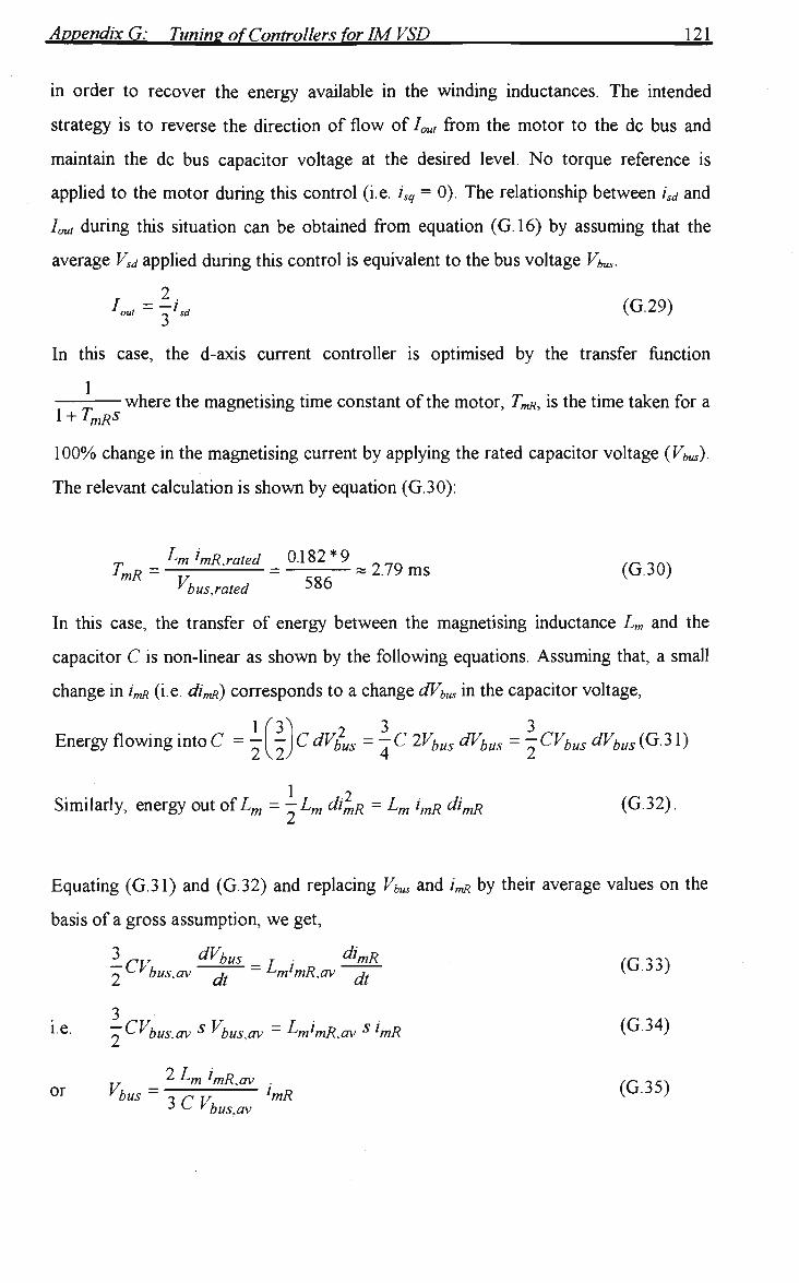
Appendix G: Tuning of Controllers for IM VSD . 121,
in order to recover the energy available in the winding inductances. The intended
strategy is to reverse the direction of flow of lout from the motor to the dc bus and
maintain the dc bus capacitor voltage at the desired level. N o torque reference is
applied to the motor during this control (i.e. isq = 0). The relationship between isd and
lout during this situation can be obtained from equation (G.l6) by assuming that the
average Vsd applied during this control is equivalent to the bus voltage Vbus-
hut = \isd (G.29)
In this case, the d-axis current controller is optimised by the transfer function
where the magnetising time constant of the motor, TmR, is the time taken for a 1 + T^S
1 0 0 % change in the magnetising current by applying the rated capacitor voltage (Vbus).
The relevant calculation is shown by equation (G.30):
™ LmimR.rated 0.182*9 TmR = -Tr = rr,, * 2.79 HIS (G.30)
v bus,rated 5 8 b
In this case, the transfer of energy between the magnetising inductance Lm and the
capacitor C is non-linear as shown by the following equations. Assuming that, a small
change in imR (i.e. dimR) corresponds to a change dVbUs in the capacitor voltage,
1
2
3 r2 3 __ 3 Energy flowing into C = - - \C dVbus =-C 2Vbus dVbus = ~CVbus dVbus (G.31)
\2J A — — UUH UUA n
1 - ,2 Similarly, energy out of Lm = -Lm dimR = Lm imR dimR (G.32)
Equating (G.31) and (G.32) and replacing Vbw! and imR by their average values on the
basis of a gross assumption, w e get,
3 rv ^bus T • dimR (GlVi 2LI/ bus,av df ~ LmlmR,av "~^~" K^.U)
3 ie- -CV b u s a v s Vbusav = LmimRav simR (G.34)
T. 2 Lm imRav or Vbus = , r v
lmR (G35) • * bus.av

Appendix G: Tuning of Controllers for IM VSD 122
The control block diagram can now be modelled as shown in Figure G.4.
""V?1 -1
^Dus
i AW
'mfln^ 1 fmf1 ^ " • « 'mf^av
* * » « •
^ .
Figure G.4 Control block diagram of an S R M V S D during bus voltage control by
recovering magnetisation energy.
The open loop transfer function (OLTF) becomes:
OLTF = Kp,b2 s + Ki,b\
s
1
}+sTsd\ 2L sd 1sd, av
\ 3CVbus> av
(G.36)
Odb
Figure G.5 Bode plot of Bus Voltage Controller 2
In this case, the bode plot has an uniform slope of -20 db/decade. The controller zero
can be placed anywhere within the allowable limits for the control to cancel the pole
and then the phase margin is always 90°. The proportional (P) and integral (I) gains are
calculated for a unity gain and a bandwidth of 119.45 rad/s, which is one-third the
corner frequency of the current loop. With a 1000 u.F bus capacitor,
OLTF = lZ-90°
(i.e.) KpM2jU9.45 + I
yl 19.45 1 +0.002355/119.45_
2*0.182*4.5
3*0.001*587 = ~J
Appendix G: Tuning of Controllers for IM VSD 123
By solving the above equation, we get:
£P.y = 0.3585
*,.«= 128.45
In the case of a 250 uF capacitor, the controller gains become:
Kpb2 = 0.09

124
APPENDED H
TUNING OF CONTROLLERS FOR SYNCHRONOUS RELUCTANCE
M O T O R VSD (SRM VSD)
(a) Speed Controller
The control loop block diagram for speed control of an SRM VSD is shown in Figure
H. 1. Full flux operation of the motor alone is considered here and field weakening is
not considered.
?l » i.
*»W*
Speed controler
r- 2
3HJ-^JMI ^
1
1+V
Current controler
-iv
s
2
h
\6 \r
+vy w 1
to
— • 1
s
p
Figure H.l. Speed control loop block diagram of an S R M V S D
From the above block diagram, it can be observed that the various control blocks
represent the operational behaviour of the S R M during speed control as described in
Subsection 2.3.2. The proportional-integral (PI) controller of the speed loop, which is
being optimised here, generates a suitable torque reference (Tref) in order to maintain
the motor at the set speed during the closed-loop control. Tref is then converted into a
current reference (isqref) as per motor torque equation (H.l) and applied to the current
controller as the control input. The closed loop operation of the current controller is
optimised by the transfer function -.—k— [26]. Here the time constant Tsq is the time l + Isqs
taken for a 1 0 0 % change in the torque producing current isq by applying the rated
voltage (Vbus) to the motor assuming that half the voltage is already available in the
motor as back emf. The calculation of Tsq is shown by equation (H.2).
TM=-Npp(Lsd-Lsq)iJ sq (H.l)

-3 Tsq L*IQ5 + J,
hq,rated 9.8 * 10"J * 19.9
bus,rated 0.5*587 664479 ps
dco = (TM~TL)dt
J
co = de_
dt
(H.2)
(H.3)
(H.4)
where,
Npp - number of pole pairs
Lsd - stator d-axis inductance
Lsq - stator q-axis inductance
isd - magnetising current
isq - torque producing current
isq.rated -stator q-axis current at rated motor torque,
Vbus.rated - rated dc bus capacitor voltage
TM - motor torque
TL - load torque,
J - moment of inertia of rotating mass
s - rotor position
The motor torque (TM), speed (co) and position (e) are calculated using equations
(H.l), (H.2) and (H.4) respectively and are represented in the relevant blocks of Figure
HI.
The open loop transfer function (OLTF) can be written as:
OLTF =
where,
G = KK sp
G Ts — KpSp
(H.5)
(H6)
(H.7)

Appendix H: Tunimr of Controllers for SRM VSD 126
The bode plot of the open loop gain has a slope of -40 db/decade except between the
two corner frequencies. The controller corner frequency is chosen such that the slope
in this interval is -20 db/decade.
The controller gains G and Ts can be chosen such that the zero db point, i.e. cross-over
frequency cocr0ss, is of the center of the section of slope -20 db/decade which gives the
maximum phase margin (53°).
-40 db/ decade
Odb
Figure H.2. Bode plot of the speed loop
In terms of the corner frequency, the optimum values of Ts and cocr0ss are [26]:
CO
T T 1SQ XS
CO, cross Ts 3Tsq 3*664479*10 -6 = 501.65 rad/s
(H.8)
(H.9)
A t COcross,
OLTF =1
i.e. G l + y'3
1 + 7 1
2T 37 Jxsq-'1sq
J = 1 (H.10)
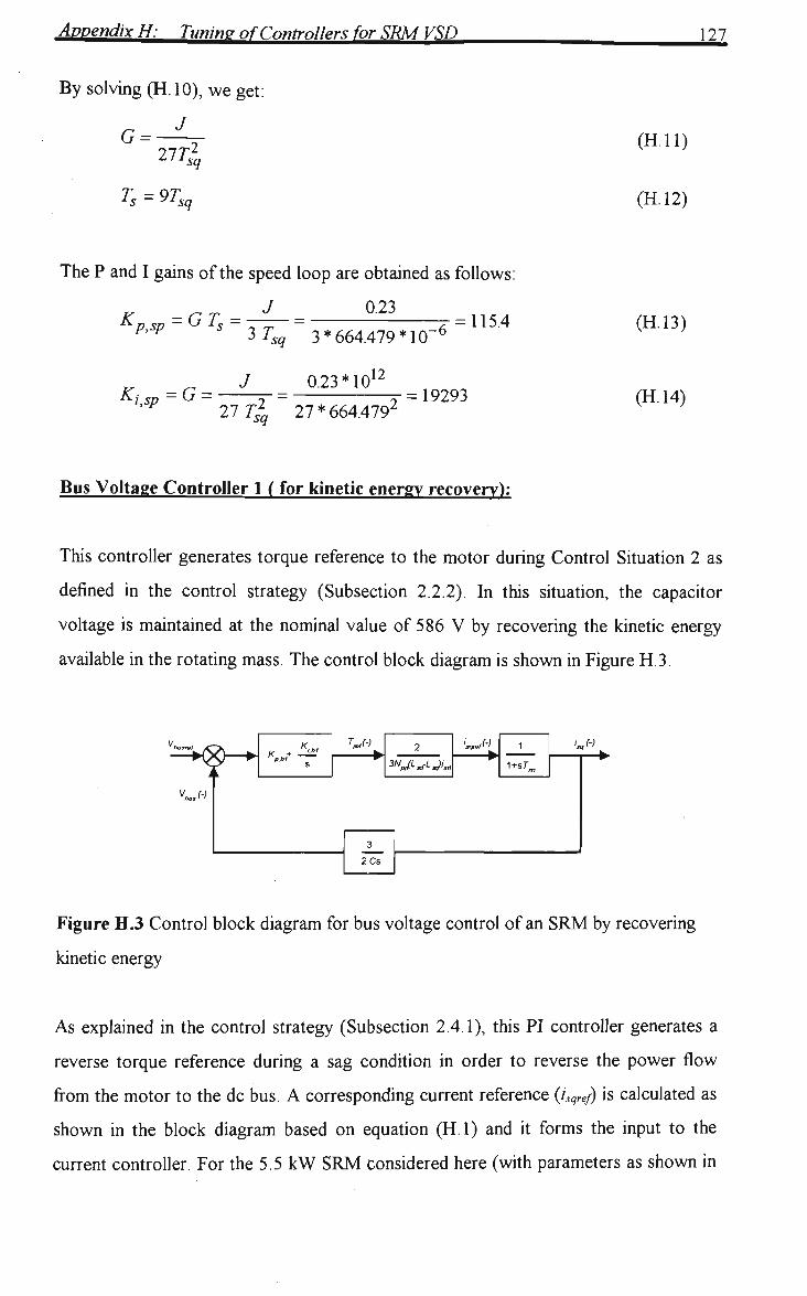
Appendix H; Tuning of Controllers for SRM VSD
By solving (H. 10), we get:
J G =
27T sq
T =9T £s VIsq
127
(H.11)
(H.12)
The P and I gains of the speed loop are obtained as follows:
J 0.23 /?,sp (-* *s ~
Ki,sp ~G =
3Tsq 3 * 664479 *10"6
J 0.23 *1012
= 115.4
i,sp 27 Tsq 27 * 664.4792
=19293
(H.13)
(H-14)
Bus Voltage Controller 1 ( for kinetic energy recovery):
This controller generates torque reference to the motor during Control Situation 2 as
defined in the control strategy (Subsection 2.2.2). In this situation, the capacitor
voltage is maintained at the nominal value of 586 V by recovering the kinetic energy
available in the rotating mass. The control block diagram is shown in Figure H.3.
vto,(->
<w Zf j^-)
3
2Cs
2
™„P-^LJ^ '«„,(-)
k-1
sq
'-«.
Figure H.3 Control block diagram for bus voltage control of an SRM by recovering
kinetic energy
As explained in the control strategy (Subsection 2.4.1), this PI controller generates a
reverse torque reference during a sag condition in order to reverse the power flow
from the motor to the dc bus. A corresponding current reference (isqref) is calculated as
shown in the block diagram based on equation (H.l) and it forms the input to the
current controller. For the 5.5 k W SRM considered here (with parameters as shown in
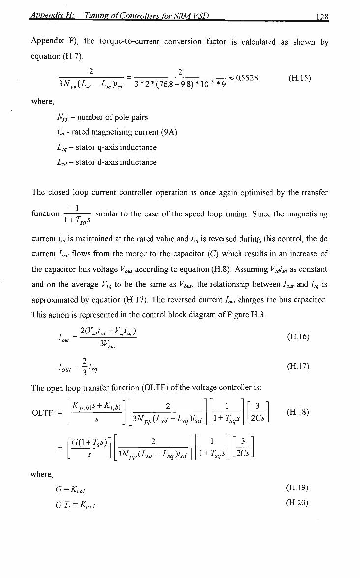
Appendix H: Tunint? of Controllers for SRM VSD 128
Appendix F), the torque-to-current conversion factor is calculated as shown by
equation (H.7).
2 2
3 # „ (4/ " 4 , >«, 3 * 2 * (76.8 - 9.8) * 10"3 * 9 * 0.5528 (H.15)
where,
Npp - number of pole pairs
isd - rated magnetising current (9A)
Lsq - stator q-axis inductance
Lsd - stator d-axis inductance
The closed loop current controller operation is once again optimised by the transfer
1 function
1 + TsqS similar to the case of the speed loop tuning. Since the magnetising
current isd is maintained at the rated value and isq is reversed during this control, the dc
current lout flows from the motor to the capacitor (C) which results in an increase of
the capacitor bus voltage Vbus according to equation (H.8). Assuming Vsdisd as constant
and on the average Vsq to be the same as Vbus, the relationship between Iout and isq is
approximated by equation (H. 17). The reversed current Iout charges the bus capacitor.
This action is represented in the control block diagram of Figure H.3.
2(Vsdisd+Vsqisq) out
3V bus
_ 2 . *out ~ o lsq
The open loop transfer function (OLTF) of the voltage controller is:
(H.16)
(HI 7)
OLTF = Kpb\s + Kf bi
G(l + Tss)
3^VpP(Tsd - Lsq)isd PP 1 + V 2Cs
(HI 8)
3Npp(Lsd ~Lsq)isd sq. i+V 2Cs
where,
G — KM
G Ts — Kp,bi
(H.19)
(H.20)
129
In the case of B u s Voltage Controller 1 also, the bode plot is similar to that the speed
loop (Figure H.2). T h e gains (G and Ts) are chosen such that the cross-over frequency
cOcross (i.e. the zero db point) is at the center of the section with a slope of -20
db/decade. A m a x i m u m phase margin of 53° is obtained.
The optimum values of Ts and cocr0ss [26] are:
1 9
T T 1sq xs
1 1 CO cross -6 Ts 3Tsq 3*664479*10"
At the cross-over frequency cocross,
OLTF = 1
Utilising equations (H. 15) and (H. 18), OLTF becomes,
= 501.65 rad/s
i.e. G|l + 7'3|
1 + 7
37^37^0.5528
2C = 1
(H.21)
(H.22)
(H.23)
(H. 24)
By solving the above equation, the proportional (P) and integral (I) gains of the Bus
Voltage Controller 1 are obtained for a bus capacitance of 1000 oF as:
A > = GTs=1.8
KM =303.6
(H.25)
(H.26)
For C=250 uF, the P and I gains become:
Kp,bi = 0.45
KM = 75.9
(H.27)
(H.28)
Bus Voltage Controller 2 (Magnetisation Energy recovery):
This controller comes into picture during Control Situation 3, i.e. in a voltage sag
condition when the motor speed is less than 1 0 % of its rated speed, as defined in the
control strategy earlier in Subsection 2.2.2. In this situation, this controller reduces the
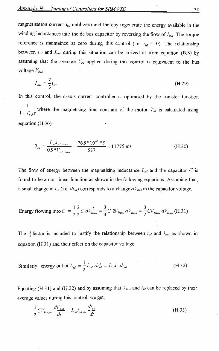
Appendix H: Tuninv of Controllers for SRM VSD 130
magnetisation current isd until zero and thereby regenerate the energy available in the
winding inductances into the dc bus capacitor by reversing the flow of IOUt. The torque
reference is maintained at zero during this control (i.e. isq = 0). The relationship
between isd and Iout during this situation can be arrived at from equation (B.8) by
assuming that the average Vsd applied during this control is equivalent to the bus
voltage Vbus-
hut = \isd (H.29)
In this control, the d-axis current controller is optimised by the transfer function
1 - — - — where the magnetising time constant of the motor Tsd is calculated using 1 + *sds
equation (H.30):
T = hdhd^d = 76.8 *10'3* 9 m §
0-5*V.ated 587
The flow of energy between the magnetising inductance Lsd and the capacitor C is
found to be a non-linear function as shown in the following equations. Assuming that,
a small change in isd (i.e. disd) corresponds to a change dVbus in the capacitor voltage,
13 3 3 Energy flowing into C = - - C dVb\s = - C 2Vbus dVbus = - CVbus dVbus (H.31)
The 4 factor is included to justify the relationship between isd and Iout as shown in
equation (H.31) and their effect on the capacitor voltage.
Similarly, energy out of Lsd = -Lsd di)d = Ljsddisd (H.32)
Equating (H.31) and (H.32) and by assuming that Vbus and isd can be replaced by their
average values during this control, w e get,
IrV ^=Li ^ 2 *"* dt " , a v dt -CVh,,^^=LJsdMV-?- (H.33)
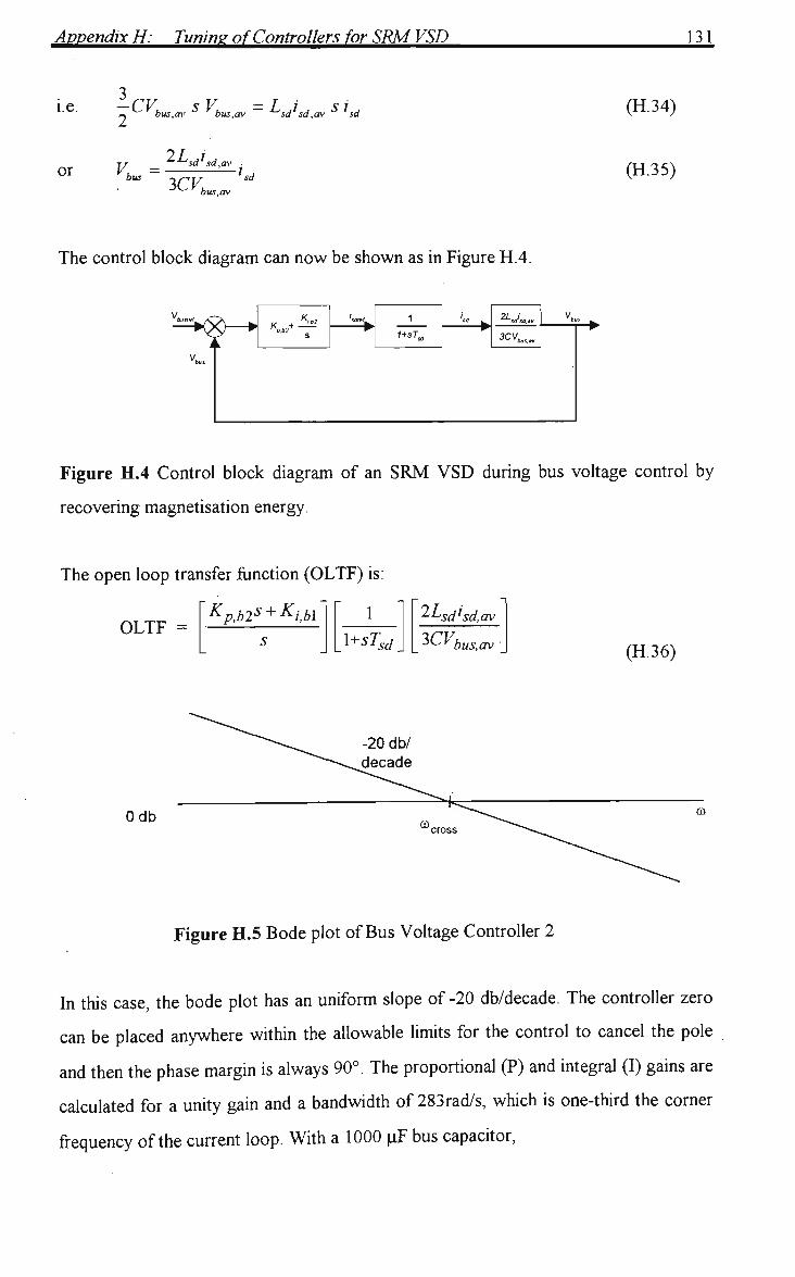
Appendix H: Tuning of Controllers for SRM VSD 131
i.e.
or
— C V sV =I i v/ ~ ^ r bus,m> * ' bus,av ^sd'sd.av * ' sd
y _ ^^sdlsd,av .
"bus ~ ~y~,Tr '** 3CV
(H.34)
(H.35) busyav
The control block diagram can now be shown as in Figure H.4.
^^Mgh-* «,„+^f 1
1*sT^
*-J«„ 3CVh„
Figure H.4 Control block diagram of an S R M V S D during bus voltage control by
recovering magnetisation energy.
The open loop transfer function (OLTF) is:
OLTF = Kp,b2S + KiM
S
1
[^Tsd\ *-L'sdlsd,av
^ " b u s . a v (H.36)
Odb
-20 db/ decade
Figure H.5 Bode plot of Bus Voltage Controller 2
In this case, the bode plot has an uniform slope of -20 db/decade. The controller zero
can be placed anywhere within the allowable limits for the control to cancel the pole
and then the phase margin is always 90°. The proportional (P) and integral (I) gains are
calculated for a unity gain and a bandwidth of 283rad/s, which is one-third the corner
frequency of the current loop. With a 1000 uF bus capacitor,
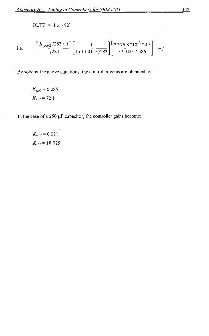
Appendix H: Tuning of Controllers for SRM VSD 132
OLTF = 1Z-900
i.e. Kpb2j2Z3 + I
7283
1 1 + 0.00115./283
2*76.8*10"3*4.5
3*0.001*586 -7
By solving the above equations, the controller gains are obtained as:
Kp,b2 = 0.085
KM = 72.\
In the case of a 250 uF capacitor, the controller gains become:
Kp,b2 = 0.021
Kub2= 18.025
133
APPENDTX I
PERFORMANCE OF SRM VSD WITH FAN TYPE LOADS
Here, the sag ride-through performance results of the proposed control strategy are
presented in the case of a Synchronous Reluctance Motor V S D ( S R M V S D ) for fan
type loads. Combined sag ride-through performance due to both kinetic and
magnetising energy recovery is analysed. The results can be compared with the results
with constant torque loads which were presented in Section 3.6 of Chapter 3.
Simulation conditions: The initial motor speed is set at 60 rad/s and the load is
configured to be proportional to the square of the motor speed with a value of 18 N m
at a speed of 120 rad/s. For a switching frequency of 5 kHz, the simulation sampling
frequency is set at 30 kHz. A 5 0 % three-phase sag is applied for 1 second.
Performance analysis: The performance characteristics, viz. motor speed (co), torque
(7A/), magnetising current (isd), capacitor voltage (Vbus) and capacitor charging current
(/,•„) of the S R M during the sag are shown in Figure 1.1. The sag condition is indicated
with a double-ended arrow along the time axis with (s) and (e) representing the start
and end of the sag. The durations of kinetic energy recovery and magnetisation energy
recovery are also indicated as 'KE' and 'ME' respectively. By comparing these results
with the constant load performance (refer Figure 3.10), it can be observed from Figure
1(a) that, the motor speed drops at a much reduced rate with fan type loads and hence
the durations of both the control modes, viz. kinetic energy and the magnetisation
energy recovery, are much longer. During magnetisation energy recovery, the observed
speed drop is very low because the load torque values at such low speeds are close to
zero. The torque and the magnetisation current response confirm the proper operation
of the control strategy during both control modes. (Figure I (b) and (c)). The capacitor
voltage is found to be close to the set-point in both modes as observed in Figure 1(d).
The capacitor recharging currents at the end of the sag are found to be within the limits
as observed in Figure 1(e). Being a fan type load, the motor speed does not go below
zero speed during this control strategy unlike constant torque loads.
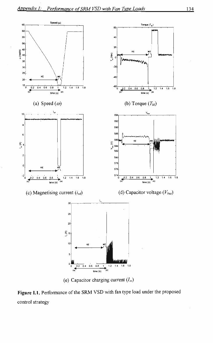
Appendix I: Performance of SRM VSD with Fan Type Loads 134
Speed (<u) Torque (T,)
time (s)
(a) Speed (co)
time (s)
(c) Magnetising current (isd)
a-15
time (s) (e)
(b) Torque (TM)
594
592
590
588
586
; 584
582
580
578
576
574
*bus
1 1 1 1 r~ — i 1 1
-If
0 0.2 0.4 0.6 0.8 1 1.2 1.4 1.6 1.1
(»> time (s) (a)
(d) Capacitor voltage (Vbus)
time (s)
(e) Capacitor charging current (/,„)
Figure 1.1. Performance of the S R M V S D with fan type load under the proposed
control strategy

135
APPENDIX J
PERFORMANCE OF AN IM VSD WITH FAN TYPE LOADS
Here, the performance results of an induction motor VSD (IM VSD) are discussed
when controlling fan type loads using the proposed strategy. Sag ride-through
performance by the two control modes, viz. recovering kinetic energy at high speeds
and the open loop flux control at lower speeds, is presented. The results can be
compared with the performance of the I M V S D with constant load torque which was
presented in Section 3.7 of Chapter 3.
Simulation conditions: A 50% three-phase sag was applied for 1 second on the IM
V S D when the motor was operating at 25 rad/s. (Here a lower initial speed was chosen
from the trials in Section 4.5 in order to observe the control transition within the 1
second sag period). A fan type load is configured with a torque of 18 N m at 120 rad/s.
Performance results: The performance characteristics, viz. motor speed (co), torque
(7A/), magnetising current (imR), capacitor voltage (Vbus) and capacitor charging current
(/,„) are shown in Figure J. 1. The sag condition is indicated as in previous cases and the
durations of kinetic energy recovery and open loop flux control are indicated as 'KE'
and 'ME' respectively. By comparing the V S D performance with the constant load
torque performance (as shown in Figure 4.10), it can be observed that, the motor
speed drops at a much reduced rate with fan type loads which is more evident during
the magnetisation energy recovery. At such low speeds, the load torque is very low.
The operation of the two control modes are verified from the response of the torque
and the magnetising current. The bus voltage is maintained at the set value during
kinetic energy recovery and drops at a slower rate during the flux reduction. Being a
fan type load, the motor speed is found not to reverse during the sag ride-through
control.

Appendix J. Performance of an IM VSD with Fan Type Loads 136
Speed (ai) Torque (T„)
time(s)
(a) Speed (co) (b) Torque (TM)
610
600
590
~ 580
3 > 570
560
550 KE
'^*— ME
vte
•w
\
•
•
— •
0 0.5
( i s — 1 1.5
(e) Sme(s)
(c) Magnetising current ( w ) (d) Capacitor voltage (Vbus)
70
60
50
40
30
20
10
KE ME
lm
•
-
•
, • , —
(if- (e) time (s)
(e) Capacitor charging current (/,„)
Figure J.l. Induction motor performance with fan type load under the control strategy
137
APPENDIX K
MATLAB PROGRAMS
a) SIMULATION OF SRM VSD
(Rating: 5.5 kW, 3 ph, 415 V AC, 50 Hz)
clc; elf; clear all;
Vpp=415; Vpk=Vpp*sqrt(2)/sqrt(3); Vsag=0.5*Vpk; Npp=2; freq=50; Ra=0.0085; La=0.0001; C=0.001; dt=0.000033; wref=120; idset=9.0; idmin=0.0; Kp=115.4; Ki=19293; TorqLt=54; Tl=18; Rs=0.6; Ld=0.0768; Lq=0.0098; J=0.23; Vbusref=586; wcutoff=15.7; BuslKp=1.8155; BuslKi=303.6; Bus2Kp=0.0849; Bus2Ki=72.1;
Vbus(l)=586; time(l)=0; IWRST=0; lab=0; lbc=0; lca=0; lout(l)=0; wact(l)=0; idact(l)=idset; iqact(l)=9.75; w=0; TQop=Tl; Tref=Tl; Pwerr=0; PVbuserr=0; id=idset; iq=9.75; Eact(l)=0; E=0; did(l)=0; diq(l)=0; Vdact(l)=0; Vqact(l)=0; % % % % fori=2:1.75/dt
time(i)=dt*i; ifi<3030
Vpeak=Vpk; elseifi>33333
CONSTANTS
% line-to-line rms voltage % line-to-neutral peak voltage % line-to-neutral peak voltage on sag % Number of pole pairs % A C Supply frequency % Per-phase line resistance % Per-phase line inductance % Bus capacitance % Sampling frequency % Velocity reference % Magnetising current (flux) reference % Minimum flux reference % Speed regulator P gain % Speed regulator I gain % Torque limit % Load torque % Stator resistance % Stator d-axis inductance % Stator q-axis inductance % System inertia % Bus Voltage reference % Cut-off velocity reference % Bus Voltage Regulator 1 P gain % Bus Voltage Regulator 1 I gain % Bus Voltage Regulator 2 P gain % Bus Voltage Regulator 2 I gain
INITIAL V A L U E S
% Capacitor voltage % Simulation time % Integrator wind-up reset (1-reset, 0-set) % Line current with phases a and b % Line current with phases b and c % Line current with phases c and a % Capacitor output current to inverter % Motor speed % Stator d-axis current % Stator q-axis current % Motor speed % Torque regulator output % Torque reference % Previous speed error % Previous dc bus voltage error % Stator d-axis current % Stator q-axis current % Rotor angle % Rotor angle % Change in stator d-axis current % Change in stator q-axis current % Stator d-axis voltage % Stator q-axis voltage
SIMULATION
Supply and sag generation

Appendix K: MA TLAB Programs 138
Vpeak=Vpk; else
Vpeak=Vsag; end;
% ac voltage waveforms (Vll)
Va=Vpeak*sin(2*pi*freq*time(i)); Vb=340*sm(2*pi*freq*tirne(iX2*pi/3)); Vc=340*sin(2*pi*freq»time(i)-(4*pi/3)); Vab(i)=Va-Vb; Vbc(i)=Vb-Vc; Vca(i)=Vc-Va; % Sense if Vll > Vbus ifVab(i)<=0
Cabl=0; elseifVab(i)>=Vbus(i-l)
Cabl=l; elseifVab(i)<=Vab(i-l)
Cabl=l; else
Cabl=0; end; % ifVab(i)>=0
Cab2=0; elseif -Vab(i)>=Vbus(i-1)
Cab2=l; elseif Vab(i)>=Vab(i-l)
Cab2=l; else
Cab2=0; end; % ifVbc(i)<=0
Cbcl=0; elseif Vbc(i)>=Vbus(i-1)
Cbcl=l; elseif Vbc(i)<=Vbc(i-1)
Cbcl=l; else
Cbcl=0; end; % ifVbc(i)>=0
Cbc2=0; elseif -Vbc(i)>=Vbus(i-1)
Cbc2=l; elseif Vbc(i)>=Vbc(i-l)
Cbc2=l; else
Cbc2=0; end; % ifVca(i)<=0
Ccal=0; elseif Vca(i)>=Vbus(i-l)
Ccal=l; elseif Vca(i)<=Vca(i-l)
Ccal=l; else
Ccal=0; end; % ifVca(i)>=0
Cca2=0; elseif - Vca(i)>=Vbus(i-1)
Cca2=l; elseif Vca(i)>=Vca(i-l)
Cca2=l; else
Cca2=0;
end; o/o Line current sensing
% PIabp=Iab+((Vab(i)-2*Ra*Iab-Vbus(i-1 ))*dt/(2*La)); PIabn=Iab+((Vab(i)-2*Ra*Iab+Vbus(i-1 ))*dt/(2*La));
if((PIabp>0)&(Cabl>0))

Appendix K: MA TLAB Programs 139
Iab=PIabp; elseif ((PIabn<0)&(Cab2>0))
Iab=PIabn; else
lab=0; end; %
PIbcp=Ibc+((Vbc(i>2*Ra*Ibc-Vbus(i-l))*dt/(2*La)); PIbcn=Ibe+((Vbc(i>2*Ra*Ibc+Vbus{i-1 ))*dt/(2*La)); if((PIbcpX))&(Cbcl>0))
Ibc=PIbcp;
elseif ((PIbcn<0)&(Cbc2>0)) Ibc=PIbcn;
else lbc=0;
end; %
PIcap=Ica+((Vca(i)-2*Ra*Ica-Vbus(i-l))*dt/(2*La)); PIcan=Ica+((Vca(i)-2*Ra*lca+Vbus(i-I))*dt/(2*U)); if((PIcaPX))&(Ccal>0))
Ica=PIcap; elseif ((PIcan<0)&(Cca2>0))
Ica=PIcan; else
lca=0; end; %
Ia(i)=Iab-Ica; Ib(i)=Ibc-Iab; Ic(i)=Ica-Ibc; Iin(i)=abs(Iab)+abs(Ibc)+abs(Ica);
"'» Capacitor voltage sensing Vbus(i)=Vbus(i-l)+((Iin(i>Iout(i-l))*dt/C); Vb=Vbus(i);
""> Speed Controller I gain selection 0/o on integrator windup reset
if IWRST==1 KI=0;
else KI=Ki;
end;
werr=wref-w; PIop=Tref+Kp*(werr-Pwerr>t-werr*KI*dt; Pwerr=weiT;
°i.TQop=PIop; °oid set=idset;
Speed Controller
Torque and flux referencing during normal ac supply
°/o Torque and flux referencing % during sag Vbuserr=Vbusref-Vb; ifVpeak==Vpk
TQop=PIop; td_set=idset;
elseif w>wcutoff Bus 1 PIop=Tref-Bus 1 Kp*( Vbuserr-PVbuserr)-Vbuserr*Bus 1 Ki*dt; TQop=BuslPIop; id_set=idset;
else Bus2PIop=idref-Bus2Kp*(Vbuserr-PVbuserr>Vbuserr*Bus2Ki*dt;
FluxPIop=-Vbuserr*FluxKp; TQop=0; id_set=Bus2PIop;
end; PVbuserr=Vbuserr, % Torque limiting/ Integrator % windup reset selection
ifTQop>TorqLt Tref=TorqLt; IWRST=1;
elseif TQop<-TorqLt Tref=-TorqLt; IWRST=1;

Appendix K: MA TLAB Programs 140
else Tref=TQop; IWRST=0;
end; % if id_set>idset
idref=idset; elseif id_set<idmin
idref=idmin; else
idref=id_set; end; % iqref^(2*Tref)/(3*Npp*(Ld-Lq)*idset); didideal=idref-id; diqideal=iqref-iq; Vdideal=Ld*(didideal/dt>w*Lq*iq; Vqideal=Lq*(diqideal/dt)+w*Ld*id; idealVreal=Vdideal*cos(E)-Vqideal*sin(E); idealVimag=Vqideal*cos(E)+Vdideal*sin(E); % Videal=sqrt((idealVreal.A2)+(idealVimag.A2)); ifVideal<%Vbus(i)/2
S=0; Real_S=0; Imag_S=0; elseif ideal Vreal>0
if(sqrt(3)*idealVimag)>idealVreal S=6; Real_S=0.5; Imag_S=0.866;
elseif (sqrt(3)*idealVimag)>-idealVreal S=4; Real_S=l; Imag S=0;
else S=5; Real_S=0.5; Imag_S=-0.866;
end; else
if(sqrt(3)*idealVimag)>-idealVreal S=2; Real_S=-0.5; Imag_S=0.866;
elseif (sqrt(3)*idealVimag)>idealVreal S=3; Real_S=-l; Imag_S=0;
else S=l; Real_S=-0.5; Imag_S=-0.866;
end; end; % RealV=Vbus(i)*Real_S: ImagV=Vbus(i)*Imag_S; Vdact(i)=RealV*cos(E)+ImagV*sin(E);
Vd=Vdact(i); Vqact(i)=ImagV*cos(E>RealV*sin(E);
Vq=Vqact(i); % did=(Vd-Rs*id+w*Lq*iq)*dtT^i; idact(i)=idact(i-l)+did;
id=idact(i); diq=(Vq-Rs*iq-w*Ld*id)*dt/Lq; iqact(i)=iqact(i-l )+diq;
iq=iqact(i); % Iout(i)=2*(Vd*id+Vq*iq)/(3*Vbus(i));
% Torqact(i)=(3/2)*Npp*(Ld-Lq)*id*iq; Torq=Torqact(i);
% dw=(Torq-Tl)*dt/J; wact(i)=wact(i-l)+dw;
w=wact(i); % dE=w*Npp*dt; Eact(i)=Eact(i-l)+dE;
E=Eact(i); end; % NN=max(size(time));MM= 15; plot(time( 1 :MM:NN).wact( 1 :MM:NN));
Flux reference limiting
Current control
Vector selection
Motor voltage calculation
Motor current calculation
Capacitor output current calculation
Motor torque calculation
Motor speed calculation
Rotor position sensing
Plot motor speed response

b) SIMULATION OF IM VSD
(Rating: 5.5 kW, 3 ph, 415 V AC, 50 Hz)
clc; elf; clear all; % % % Vpp=415; Vpk=Vpp*sqrt(2)/sqrt(3); Vsag=0.5*Vpk; Npp=2; freq=50; Ra=0.0085; La=0.0001; C=0.001; dt=0.000033; wref=120; imRref=9.0000; imRmin =0.0; Kp=148; Ki=31671; TorqLt=54: Ti=I8; Rs=0.673 Rr=1.2964; J=0.23: Vbusref=586; wcutoff=15.7; sigs=0.0484; sigr=0.0484; Lm=0.182: BuslKp=2.68; BuslKi=573.75: Bus2Kp=0.3585; Bus2Ki=128.45;
Ls=Lm*(l+sigs); Lr=Lm*(l+sigr); % Tr=Lr/Rr,
sigma= 1 -(1 /((1 +sigs)*( 1 +sigr))); % K=2*Lm/(3*(l+sigr));
Vbus(l)=586: time(l)=0; IWRST=0; lab=0; lbc=0; lca=0; lout(l)=0; wact(l)=0; w=0; idact(l)=idset; iqact(l)=9.75; id=idset; iq=9.75; irqact(l)=0; imRact( 1 )=imRref; imR=imRref; imR_ref=imRref; TQop=Tl: Tref=Tl; Pwerr=0; PVbuserr=0; Eact(l>=0; E=0; did(l)=0;
CONSTANTS
% line-to-line rms voltage % line-to-neutral peak voltage % line-to-neutral peak voltage on sag % Number of pole pairs % A C Supply frequency % Per-phase line resistance % Per-phase line inductance % Bus capacitance % Sampling frequencywref=120; % Velocity reference % Magnetising current (flux) reference % Minimum flux reference % Speed regulator P gain % Speed regulator I gain % Torque limit % Load torque % Stator resistance % Rotor resistance % System inertia % Bus Voltage reference % Cut-off velocity reference % Stator leakage factor % Rotor leakage factor % Mutual inductance % Bus Voltage Regulator 1 P gain % Bus Voltage Regulator 1 I gain % Bus Voltage Regulator 2 P gain % Bus Voltage Regulator 2 I gain
CALCULATED VALUES
Leakage inductances
Rotor time constant
Total leakage factor
Torque constant
INITIAL V A L U E S
% Capacitor voltage % Simulation time % Integrator wind-up reset (1-reset, 0-set) % Line current with phases a and b % Line current with phases b and c % Line current with phases c and a % Capacitor output current to inverter % Motor speed % Motor speed % Stator d-axis current % Stator q-axis current % Stator d-axis current % Stator q-axis current % Rotor q-axis current % Rotor magnetising current % Rotor magnetising current % Rotor magnetising current reference % Torque regulator output % Torque reference % Previous speed error % Previous dc bus voltage error % Rotor angle % Rotor angle % Change in stator d-axis current

Appendix K: MA TLAB Programs 142
diq(l)=0; Vdact(l)=0; Vqact(l)=0; wmRact(l)=0; P=0; dP=0; wmR=0; dimR=0; PdimRideal=0; Pidref=imRref; imRset=imRref, PimRset=imRref;
% Change in stator q-axis current % Stator d-axis voltage % Stator q-axis voltage % Speed of magnetising reference frame % Position of magnetising reference frame % Change in flux velocity % Speed of magnetising reference frame % Change in magnetising current % Previous required change in imR % Previous Stator d-axis current reference % magnetising current reference
SIMULATION
Supply and sag generation
for i=2:0.2/dt time(i)=dt*i; ifi<3030 Vpeak=340; elseif i>33333 Vpeak=340; else Vpeak=340; end;
Va=Vpeak*sin(2*pi*freq*time(i)); Vb=340*sin(2*pi*freq*time(i)-(2*pi/3)); Vc=340*sin(2*pi*freq*time(iH4*pi/3)); Vab(i)=Va-Vb; Vbc(i)=Vb-Vc; Vca(i)=Vc-Va; % ifVab(i)<=0 Cabl=0; elseif Vab(i)>=Vbus(i-1) Cabl=l; elseif Vab(i)<=Vab(i-l) Cabl=l; else Cab 1=0; end; ifVab(i)>=0 Cab2=0; elseif-Vab(i)>=Vbus(i-l)
Cab2=l; elseifVab(i)>=Vab(i-l) Cab2=l; else Cab2=0; end: ifVbc(i)<=0 Cbcl=0; elseif Vbc(i)>=Vbus(i-1)
Cbcl = l: elseif Vbc(i)<=Vbc(i-l)
Cbcl = l; else Cbcl=0; end; ifVbc(i)>=0 Cbc2=0; elseif-Vbc(i)>=Vbus(i-l)
Cbc2=l; elseif Vbc(i)>=Vbc(i-l)
Cbc2=l: else Cbc2=0; end; ifVca(i)<=0 Ccal=0; elseif Vca{i)>=Vbus(i-l)
Ccal = l; elseif Vca(i)<=Vca(i-l)
Ccal=l; else Cca 1=0; end; ifVca(i)>=0 Cca2=0;
Line-to line ac voltages (Vll)
Sensing when Vll > Vbus

Appendix K: MA TLAB Programs 143_
elseif -Vca(i)>=Vbus(i-1) Cca2=l; elseif Vca(i)>=Vca(i-1) Cca2=l; else Cca2=0; end;
% Line current sensing %
PIabp=Iab+((Vab(i>2*Ra*Iab-Vbus(i-l))*dt/(2*La)); PIabn=Iab+((Vab(i>2*Ra*Iab+Vbus(i-l))*df(2*La)); if ((PIabp>0)&(Cab 1 >0)) Iab=PIabp; elseif ((PIabn<0)&(Cab2>0)) Iab=PIabn; else lab=0; end; PIbcp=Ibc+((Vbc(i>2*Ra*Ibc-Vbus(i-l))*dt/(2*La)); PIbcn=Ibc+((Vbc(i)-2*Ra*Ibc+Vbus(i-1 ))*dt/(2*La)); if((PIbcp>0)&(Cbcl>0)) Ibc=PIbcp; elseif ((PIbcn<0)&(Cbc2>0)) Ibc=PIbcn; else lbc=0; end; PIcap=Ica+((Vca(i>2*Ra*Ica-Vbus(i-l))*dt/(2*La)); PIcan=Ica+((Vca(i>2*Ra*Ica+Vbus(i-l ))*dt/(2*La)); if ((PIcap>0)&(Ccal >0)) Ica=PIcap;
elseif ((PIcan<0)&(Cca2>0)) lca=PIcan; else lca=0; end; %Ia(i)=Iab-Ica; %Ib(i)=Ibc-Iab;
%Ic(i)=Ica(i)-It>c(i); Iin(i)=abs(Iab)+abs(Ibc)+abs(Ica); % Capacitor voltage sensing Vbus(i)=Vbus(i-1 )+(Iin(i)-Iout(i-1 ))*dt/C; Vb=Vbus(i); % Speed Controller 1 gain selection % on integrator windup reset
i f I W R S T = l KI=0; else KI=Ki; end; % Speed Controller
werr=wref-w; PIop=Tref+Kp*(werr-Pwerr)+werr*KI*dt; Pwerr=werr, Vbuserr=Vbusref-Vb;
% Bus Voltage Controllers 1 & 2
% Bus 1 PIop=Tref-Bus 1 Kp*( Vbuserr-PVbuserr)-Vbuserr*Bus 1 Ki*dt; Bus2PIop=imR_ref-Bus2Kp*(Vbuserr-PVbuserr)-Vbuserr*Bus2Ki*dt;
PVbuserr=Vbuserr, ifBus2PIop>imRref B2PIop=imRref; elseif Bus2PIop<imRmin
• B2PIop=imRmin; else B2PIop=Bus2PIop; end; «/„ Torque and flux referencing % during normal ac supply
%TQop=PIop; %imR_ref=imRref; o/0 Torque and flux referencing o/o during a sag
if((Vpeak==Vpk)&(imR>=imRref*0.975))
TQop=PIop; imR_ref=imRref; elseif Vpeak==Vpk TQop=0; imR_ref=imR+((imR*dt)/(2*Tr));
elseif w>wminref TQop=BuslPIop; imR_ref=imRref; else TQop=0;
% irnR_ref=imR+((B2PIop-imR)*dt/Tr); imR_ref=imR-((irnR*dty(2*Tr)); end; % /o Torque limiting/ Integrator '" windup reset selection ifTQop>TorqLt Tref=TorqLt; IWRST=1; elseifTQop<-TorqLt Tref=-TorqLt; IWRST=1; else Tref=TQop; IWRST=0; end; 0/0 Flux reference limiting if imR_ref>imRref imR_set=imRref, elseif imR_ref<imRmin imR_set=imRmin; else imR_set=imR_ref; end; 0/0 Current control iqref=Tref/(Npp*K*imR); %dimRideal=imRset-imR; dirnRideal=imR_set-imR;
%id_ref=Hdref+Kpflux*(dirru^ideal-PdimRideal)+dimRideal*Kiflux*dt; id_ref=imR_set+(dimRideal/dt)*Tr, if id_ref>idmax idref=idmax; elseif id_ref<idmin idrefNdmin; else idref=id_ref; end; Pidref=idref; PdimRideal=dimRideal; didideal=idref-id; diqideal=iqref-iq;
Vdideal=(Rs*id)+(sigma*Ls)*((didideal/dt)-(wmR*iq))+((l-sigma)*Ls*dimRideal/dt); Vqideal=(Rs*iq)+(sigma*Ls)*((diqideal/dt)+(wmR*id))+((l-sigma)*Ls*wmR*imR); idealVreal=Vdideal*cos(P)-Vqideal*sin(P); idealVimag=Vqideal*cos(P)+Vdideal*sin(P); % % Vector selection % Videal=sqrt((idealVreal.A2)+(ideaIVimag.A2)); if VideaK Vbus(i)/2
S=0;Real_S=0;Imag_S=0; elseif ideal Vreal>0
if(sqrt(3)*ideaIVimag)>idealVreal S=6;Real_S=0.5;Imag_S=0.866; elseif (sqrt(3)*idealVimag)>-idealVreal S=4;Real_S=l;Imag_S=0; else S=5;Real_S=0.5;Imag_S=-0.866; end;
else if(sqrt(3)*idealVimag)>-idealVreal S=2;Real S=-0.5;Imag_S=0.866; elseif (sqrt(3)*idealVimag)>idealVreal
S=3 ;Real_S=-1 ;Imag_S=0; else S= I ;Real_S=-0.5 ;Imag_S=-0.866; end;
end; % Motor voltage calculations
RealV=Vbus(i)*Real_S; ImagV=Vbus(i)*Imag_S;
Appendix K: MATLAB Programs 145
Vd=RealV*cos(P)+ImagV*sin(P); Vq=ImagV*cos(P>RealV*sin(P);
Motor current calculations
did^((Vd-Rs*id-((l-sigma)*Ls*dirnR/dt))/(Ls*sigma))+wmR*iq)*dt; idact(i)=idact(i-1 )+did; id=idact(i); diq=(((Vq-Rs*iq-((l-sigma)*Ls*wmR*imR))/(Ls*sigma)>wmR*id)*dt; iqact(i)=iqact(i-l )+diq; iq=iqact(i);
Iout(i)=2*(Vd*id+Vq*iq)/(3*Vbus(i)); % dimR=(id-imR)*dt/Tr, imRact(i)=imRact(i-l )+dimR; imR=imRact(i); % Torqact(i)=Npp*K*imRact(i)*iqact(i); Torq=Torqact(i); % dw=(Torq-Tl)*dt/J; wact(i)=wact(i-1 )+dw; w=wact(i); °/0
slip=iqact(i)/(Tr*imRact(i)); wmRact(i)=wact(i)+slip; wmR=wmRact(i); % dP=wmR*Npp*dt; P=P+dP;
%irdact(i)=-Lm*dimR/(Rr*dt); %irqact(i)=Lm*imR*(w-wmR)/Rr, % %isreal=(id*cos(P>iq*sin(P)); %isimag=iq*cos(P)+id*sin(P); %isl(i)=2*isreal/3; °/ois2(i)=-(isreal/3)+(isimag/l .732); %is3(i)=-(isreal/3)-('simag/l .732);
Capacitor output current calculation
Magnetising current calculation
Motor torque calculation
Motor velocity calculation
Slip and flux velocity calculation
Flux axis position calculation
Rotor current calculations
Motor terminal current waveform
end: % NN=max(size(time));MM= 15; plot(time(l:MM:NN),wact(l:MM:NN));
Plot motor velocity