196 IEEE TRANSACTIONS ON BIOMEDICAL CIRCUITS AND …mdker/Referred Journal Papers/2013 TBCAS... ·...
8
196 IEEE TRANSACTIONS ON BIOMEDICAL CIRCUITS AND SYSTEMS, VOL. 7, NO. 2, APRIL 2013 Implantable Stimulator for Epileptic Seizure Suppression With Loading Impedance Adaptability Chun-Yu Lin, Member, IEEE, Wei-Ling Chen, and Ming-Dou Ker, Fellow, IEEE Abstract—The implantable stimulator for epileptic seizure suppression with loading impedance adaptability was proposed in this work. The stimulator consisted of the high voltage generator, output driver, adaptor, and switches, can constantly provide the required 40- stimulus currents, as the loading impedance varied within 10 –300 . The performances of this design have been successfully verified in silicon chip fabricated by a 0.35- 3.3-V/24-V CMOS process. The power consumption of this work was only 1.1 mW–1.4 mW. The animal test results with the fabricated chip of proposed design have successfully verified in the Long-Evans rats with epileptic seizures. Index Terms—Adaptability, epilepsy, epileptic seizure suppres- sion, implantable device, stimulator. I. INTRODUCTION T HERE are of the people in the world affected by the epilepsy [1], [2]. This disease is caused by transient abnormal discharge in brain, and it is one of the common neuro- logical diseases [3]–[5]. If this seizure cannot be well controlled, the patients will be affected in sensations, emotions, memories, and other related activities. Typically, the epileptic seizure can be treated by pharmacologic or surgical treatments. The most common way to suppress epileptic seizure is the pharmacologic treatment [6]–[8]. There are more than 20 types of medications for specific types of epileptic seizures. However, there are still many patients who can not be cured by the medications [9]. For these medically refractory patients, an alternative is the sur- gical treatment [10]–[12]. In this treatment, some tissues with abnormal discharge will be removed from the brain. It is a risky treatment because patients may loss some physical functions permanently after taking the surgery. In addition, some patients still can not be completely cured by the surgery [13], [14]. In recent years, the new techniques of electrical stimulation, such as the vagus nerve stimulation and deep brain stimulation [15]–[17], have been demonstrated to suppress the abnormal discharge signal before epileptic seizure happen. Comparing Manuscript received January 30, 2012; revised April 30, 2012; accepted May 14, 2012. Date of publication July 03, 2012; date of current version May 03, 2013. This work was supported by National Science Council (NSC), Taiwan, under Contract of NSC 101-2220-E-009-020, and by the “Aim for the Top Uni- versity Plan” of National Chiao-Tung University and Ministry of Education, Taiwan. This paper was recommended by Associate Editor M. Sawan. The authors are with the Nanoelectronics and Gigascale Systems Laboratory, Institute of Electronics, National Chiao-Tung University, Hsinchu 300, Taiwan, and also with the Biomedical Electronics Translational Research Center, Na- tional Chiao-Tung University, Hsinchu 300, Taiwan (e-mail: [email protected]; [email protected]). Color versions of one or more of the figures in this paper are available online at http://ieeexplore.ieee.org. Digital Object Identifier 10.1109/TBCAS.2012.2200481 Fig. 1. Block diagram of implantable device for epileptic seizure suppression. with the traditional treatments, the electrical stimulation is more harmless, flexible, recoverable, and less-destructive [18], [19]. Therefore, many epilepsy control systems by using electrical stimulation have been studied. Fig. 1 shows the functional block diagram of a closed-loop epileptic seizure monitoring and con- trolling system in an implantable device [20]–[22]. This im- plantable device consists of the detector, signal processor, and stimulator to form a closed-loop seizure controller. In the animal test of Long-Evans rats with epileptic seizures shown in [20], the required stimulus current to suppress the seizure is found to be 40 . Besides, due to different tissues, locations, distances, and implanted time, the effective loading impedance of stimulator will vary from 100 to 250 . Therefore, the stimulator with loading impedance adaptability is needed. To deliver the stimulus current with the varied loading impedance, some approaches have been studied. For example, the stimulator can monitor the loading impedance first, and then setting the operating voltage [23], [24]. Of course, the moni- toring circuit adds more area and complexity to the stimulator. In this work, the integrated circuit design of implantable stim- ulator for epileptic seizure suppression with loading impedance adaptability and low power consideration is proposed [25]. This proposed stimulator can deliver bi-phasic stimulus currents by two leads electrode per stimulus site [26] with single supply voltage . The required high voltage of stim- ulator can be adjusted to reduce the power consumption. The detailed design procedures of the stimulator will be presented in Section II. A 0.35- 3.3-V/24-V CMOS process is used 1932-4545/$31.00 © 2012 IEEE
Transcript of 196 IEEE TRANSACTIONS ON BIOMEDICAL CIRCUITS AND …mdker/Referred Journal Papers/2013 TBCAS... ·...

196 IEEE TRANSACTIONS ON BIOMEDICAL CIRCUITS AND SYSTEMS, VOL. 7, NO. 2, APRIL 2013
Implantable Stimulator for Epileptic SeizureSuppression With Loading Impedance Adaptability
Chun-Yu Lin, Member, IEEE, Wei-Ling Chen, and Ming-Dou Ker, Fellow, IEEE
Abstract—The implantable stimulator for epileptic seizuresuppression with loading impedance adaptability was proposed inthis work. The stimulator consisted of the high voltage generator,output driver, adaptor, and switches, can constantly provide therequired 40- stimulus currents, as the loading impedancevaried within 10 –300 . The performances of this designhave been successfully verified in silicon chip fabricated by a0.35- 3.3-V/24-V CMOS process. The power consumption ofthis work was only 1.1 mW–1.4 mW. The animal test results withthe fabricated chip of proposed design have successfully verifiedin the Long-Evans rats with epileptic seizures.
Index Terms—Adaptability, epilepsy, epileptic seizure suppres-sion, implantable device, stimulator.
I. INTRODUCTION
T HERE are of the people in the world affected bythe epilepsy [1], [2]. This disease is caused by transient
abnormal discharge in brain, and it is one of the common neuro-logical diseases [3]–[5]. If this seizure cannot bewell controlled,the patients will be affected in sensations, emotions, memories,and other related activities. Typically, the epileptic seizure canbe treated by pharmacologic or surgical treatments. The mostcommon way to suppress epileptic seizure is the pharmacologictreatment [6]–[8]. There are more than 20 types of medicationsfor specific types of epileptic seizures. However, there are stillmany patients who can not be cured by the medications [9].For these medically refractory patients, an alternative is the sur-gical treatment [10]–[12]. In this treatment, some tissues withabnormal discharge will be removed from the brain. It is a riskytreatment because patients may loss some physical functionspermanently after taking the surgery. In addition, some patientsstill can not be completely cured by the surgery [13], [14].In recent years, the new techniques of electrical stimulation,
such as the vagus nerve stimulation and deep brain stimulation[15]–[17], have been demonstrated to suppress the abnormaldischarge signal before epileptic seizure happen. Comparing
Manuscript received January 30, 2012; revised April 30, 2012; accepted May14, 2012. Date of publication July 03, 2012; date of current version May 03,2013. This work was supported by National Science Council (NSC), Taiwan,under Contract of NSC 101-2220-E-009-020, and by the “Aim for the Top Uni-versity Plan” of National Chiao-Tung University and Ministry of Education,Taiwan. This paper was recommended by Associate Editor M. Sawan.The authors are with the Nanoelectronics and Gigascale Systems Laboratory,
Institute of Electronics, National Chiao-Tung University, Hsinchu 300, Taiwan,and also with the Biomedical Electronics Translational Research Center, Na-tional Chiao-Tung University, Hsinchu 300, Taiwan (e-mail: [email protected];[email protected]).Color versions of one or more of the figures in this paper are available online
at http://ieeexplore.ieee.org.Digital Object Identifier 10.1109/TBCAS.2012.2200481
Fig. 1. Block diagram of implantable device for epileptic seizure suppression.
with the traditional treatments, the electrical stimulation is moreharmless, flexible, recoverable, and less-destructive [18], [19].Therefore, many epilepsy control systems by using electricalstimulation have been studied. Fig. 1 shows the functional blockdiagram of a closed-loop epileptic seizure monitoring and con-trolling system in an implantable device [20]–[22]. This im-plantable device consists of the detector, signal processor, andstimulator to form a closed-loop seizure controller.In the animal test of Long-Evans rats with epileptic seizures
shown in [20], the required stimulus current to suppress theseizure is found to be 40 . Besides, due to different tissues,locations, distances, and implanted time, the effective loadingimpedance of stimulator will vary from 100 to 250 .Therefore, the stimulator with loading impedance adaptabilityis needed.To deliver the stimulus current with the varied loading
impedance, some approaches have been studied. For example,the stimulator can monitor the loading impedance first, and thensetting the operating voltage [23], [24]. Of course, the moni-toring circuit adds more area and complexity to the stimulator.In this work, the integrated circuit design of implantable stim-
ulator for epileptic seizure suppression with loading impedanceadaptability and low power consideration is proposed [25]. Thisproposed stimulator can deliver bi-phasic stimulus currents bytwo leads electrode per stimulus site [26] with single supplyvoltage . The required high voltage of stim-ulator can be adjusted to reduce the power consumption. Thedetailed design procedures of the stimulator will be presentedin Section II. A 0.35- 3.3-V/24-V CMOS process is used
1932-4545/$31.00 © 2012 IEEE

LIN et al.: IMPLANTABLE STIMULATOR FOR EPILEPTIC SEIZURE SUPPRESSION WITH LOADING IMPEDANCE ADAPTABILITY 197
Fig. 2. Block diagram of stimulator with loading impedance adaptability.
in this work for the chip implementation. The measurement re-sults in silicon chip will be presented in Section III. The com-parison among the reported on-chip stimulators in recent litera-ture [27]–[29] and this design will be summarized in Section IV.The animal test results in the closed-loop epileptic seizure mon-itoring and controlling system will be presented in Section V.
II. PROPOSED STIMULATOR DESIGN
Fig. 2 shows the proposed stimulator, which consists ofa high voltage generator, an output driver, an adaptor, andswitches. The proposed stimulator adopts two leads electrodeset per stimulus site (electrode 1 and electrode 2) to generatebi-phasic stimulus currents. Once the detector of implantabledevice in Fig. 1 detects the epileptic seizure, the stimulator be-comes active. Under stimulation, the positive stimulus current
will flow through the output driver, electrode 1, braintissue, electrode 2, and adaptor, while the negative stimuluscurrent will flow through the output driver, electrode2, brain tissue, electrode 1, and adaptor. The high voltagegenerator is used to supply the variable voltage to outputdriver, and it is controlled by the feedback signal from adaptor(Ctrl.). Since the targeted stimulus current is 40 and theloading impedance varies from 100 to 250 , the voltagedifference between two electrodes is between 4 V and 10 V. Inother word, the required supply voltage for output drivermust be as high as 10 V, which is much higher than the supplyvoltage . Therefore, the high voltage generatoris used to provide the variable high voltage. To reduce thepower consumption in stimulator, the high voltage generatorcan output the different voltage level according to the differentloading impedance.The design and operation of the output driver, adaptor, high
voltage generator, and switches will be discussed in followingparagraphs.
Fig. 3. Schematic circuits of output driver and adaptor.
A. Output Driver
The schematic circuits of the output driver and adaptor areshown in Fig. 3. In the output driver, the stimulus current sourceconsists of a current mirror (Mp1 and Mp2) and bias circuit(Mn1, Mn2, Mn3, Mp3, and ). The 3.3-V supply voltage
, variable voltage , and stimulation signal (Stim.)are used in this circuit. The is used to provide the biasvoltage for the gate terminal of Mn1. During the stimulation“on” interval, the stimulation signal is high ,Mn2 is turned off, Mp3 is turned on, and Mn1 is biased throughMp3. The Mn1 is biased to operate in saturation region understimulation. The Mp1 and Mp2 are also designed to operate insaturation region under stimulation. The voltage will in-crease or decrease to keep delivering 40- stimulus current
under stimulation. Besides, if the is initially storedat higher voltage and applied to the lower loading impedance,the can limit the at . The can also pre-vent the tissue from large glitch current. During the stimulator“off” interval, the stimulation signal is low . Mn2is turned on and Mn1 is turned off, so there is no stimulus cur-rent delivered.
B. Adaptor
The adaptor of stimulator consists of a current mirror (Mn4and Mn5), resistor (R1), and comparator (C1), as shownin Fig. 3. During the stimulation “on” interval, the positive(negative) stimulus current passes through tissue and elec-trode 2 (electrode 1), and then flows into the adaptor. In the

198 IEEE TRANSACTIONS ON BIOMEDICAL CIRCUITS AND SYSTEMS, VOL. 7, NO. 2, APRIL 2013
Fig. 4. Low-power comparator used in adaptor.
meantime, the positive or negative stimulus currentflows into the Mn4 of current mirror. The gate terminal ofMn5 is biased to induce the proportional current .In this work, the Mn4 and Mn5 are designed to keep the
equal to . The adaptor utilizes flowingthrough resistor to generate a voltage signal
. Another voltage signal whichis used to compare with is . Since the voltageis kept at , it can be divided from . Wheneverthe stimulator is turned on to stimulate the brain tissue, thecomparator in the adaptor compares these two voltage signals( and ) and distinguishes the amplitude of stimulus current.The variable supply voltage for output driver can becontrolled by the output of comparator (Ctrl.). If the islower than 40 , which leads to higher than , the outputof comparator will become high . The highvoltage generator will keep pumping to provide higher voltageuntil the reaches 40 . Once the is higherthan 40 , which leads to lower than , the output ofcomparator will become low . The high voltagegenerator will stop pumping to provide lower voltage until the
returns 40 . The feedback design of adaptor keepsthe stimulus current at .The comparator used in the adaptor is shown in Fig. 4 [30].
Under stimulation , the comparator turns on.When the clock signal is low, the comparator is pre-charged,and there is no dc current path from power to ground. Whenthe clock is high, the comparator compares the and , andthe feedback loop latches the comparator into steady state. Insteady state of comparator, there is also no dc current path frompower to ground. The comparator without dc current is verypower-saving.During the stimulator “off” interval, the stimulation signal
(Stim.) is equal to 0 V, so the last-stage inverter of comparatoroutputs high signal . Even so, the Stim. stopsthe high voltage generator from pumping to high voltage in thisinterval.
C. High Voltage Generator
The high voltage generator of stimulator uses thecharge-pump-based circuit, as shown in Fig. 5(a). The highvoltage generator consists of the 4-stage charge pump circuit,
Fig. 5. Design of (a) high voltage generator and (b) 4-stage charge pump cir-cuit.
clock controller, clock buffers, and output capacitor .The clock controller is utilized to generate the frequency-mod-ulated clock signal (Clk) which depends on the reference clocksignal (Clock), stimulation signal (Stim.), and the feedbacksignal from comparator (Ctrl.).During the stimulator “on” interval, the stimulation signal is
high, and the clock controller starts to send the frequency-mod-ulated clock signal to the 4-stage charge pump circuit. If theCtrl. signal is low, the reference clock signal is modulated tothe lower-frequency output (Clk). Likewise, if the Ctrl. signal ishigh, the reference clock signal is modulated to the higher-fre-quency Clk. During the stimulator “off” interval, the stimulationsignal is low , and the Clk signal also keeps at 0 V,so the 4-stage charge pump circuit stops pumping.The used 4-stage charge pump circuit is shown in Fig. 5(b).
This charge pump circuit has been studied to output the highvoltage , but it will not suffer the gate-oxide reliabilityissue [31]. There is a compromise between capacitor sizeand clock frequency, so the used reference clock frequency is25 MHz, and each capacitor in 4-stage charge pump is 15 pF.The output voltage of the 4-stage charge pump circuitwith 3.3-V supply can be ideally pumped up to .At the beginning of operation, there is no charge stored at
the output capacitor of high voltage generator, and theoutput voltage is initially 0 V. Under stimulation, the

LIN et al.: IMPLANTABLE STIMULATOR FOR EPILEPTIC SEIZURE SUPPRESSION WITH LOADING IMPEDANCE ADAPTABILITY 199
charge pump circuit starts to pump to high voltage. If the Ctrl.signal is high, the charge pump circuit keeps pumping to highervoltage. Therefore, the output voltage of high voltage gener-ator increases, and stimulus voltage is delivered from the chargepump. The charge pump circuit keeps pumping until the stim-ulus current is slightly higher than 40 to cause that islower than in the adaptor, that is to say, the Ctrl. signal be-comes low. The inactivated charge pump circuit causes thatoutput voltage of high voltage generator and stimulus currentdecrease. Therefore, by changing the state of charge pump cir-cuit instantaneously, the output voltage of high voltage gener-ator keeps at the required high voltage.During the stimulator “off” interval, the Clk signal keeps at
low to inactive the charge pump circuit. Although the chargepump circuit stops pumping, some charges still store in theoutput capacitor to keep the at higher voltagewithin a short time. The used in this work is 15 pF, andthe time constant to discharge the during the stimulator“off” interval is .
D. Switches
The switches are used to conduct positive and negative stim-ulus currents ( and ). Besides stimulation inter-vals, the switches are shorted to ground to prevent from chargeaccumulation in brain tissue.
E. Simulation Results
The proposed stimulator has been simulated in HSPICEwith the 0.35- 3.3-V/24-V CMOS process. Fig. 6 showsthe voltage/current waveforms of , tissue, and as onestimulation with loading impedance is 300 . During0–2 , the stimulation signal is low, and the stimulus currentkeeps at 0 A. In the same duration, the is initially set at3 V, which simulates the voltage stored in the output capac-itor from previous stimulation. During 2–10 , thestimulation signal is high, and the stimulus current is sent. Therequired time for stimulus current to reach 40 is 1.26 .After that, the stimulus current keeps at once thestimulation signal keeps at high. In this time period, the voltageof moves around , and the voltage of alsomoves around , as shown in Fig. 6(a). Although it seemsan oscillation, the waveform is controlled by the adaptor. Asis higher than , the high voltage generator pumps theto higher voltage. While is lower than , the high
voltage generator stops pumping, so the decreases. Thestability and reliability of this circuit have been considered indesign phase [32]. In this stimulation of current pulses with
amplitude, 0.5-ms pulse width, 2.5-ms period, and0.5-s duration, the total power consumption of the stimulatoris 0.9 mW in which 0.6 mW is consumed in the high voltagegenerator, 0.11 mW is consumed in the output driver, 0.1 mWis consumed in the adaptor, and 0.09 mW is consumed in theswitches.The stimulation with different loading impedance is also sim-
ulated. The stimulus current always keeps at as theloading impedance varies from 10 to 300 . The simulated
as the loading impedance varies from 10 to 300
Fig. 6. Simulated voltage/current waveforms of (a) , (b) , and(c) , as loading impedance is 300 .
are 7–14 V. The efficiency of high voltage generator calculatedaccording to [33] is . The total power consumption ofthe stimulator is 0.4–0.9 mW, as shown in Fig. 7. Fig. 7 alsocompares the power consumption of the traditional design withconstant and that of the proposed design with adaptor toadjust voltage. Although additional power is consumed inthe adaptor, the proposed design can reduce the total power con-sumption in low impedance region.
III. VERIFICATION IN SILICON CHIP
The proposed bi-phasic stimulator to suppress epilepticseizure with loading impedance adaptability and low-powerconsideration has been fabricated in the 0.35- 3.3-V/24-VCMOS process. Fig. 8 shows the chip photograph of the fabri-cated stimulator. The occupied area of the proposed stimulator

200 IEEE TRANSACTIONS ON BIOMEDICAL CIRCUITS AND SYSTEMS, VOL. 7, NO. 2, APRIL 2013
Fig. 7. Simulated total power consumption of stimulator as loading impedancevaries from 10 to 300 .
Fig. 8. Chip photograph of fabricated chip.
is about 1000 700 . The chip has been assembled inpackage for measurement.Under measurement, Agilent E3631A is used to provide the
fixed 3.3-V . Hp 33120A is used to supply the 25-MHzreference clock signal and to send the stimulation signal. Tek-tronix 3054B is used to observe the stimulus voltage/current inthe loading.While stimulation signal is given, the proposed design starts
to deliver the stimulus current. Fig. 9 shows the stimulus cur-rent with 300- loading impedance. In this stimulation, themeasured waveforms of , , and duringare shown in Fig. 10. In this duration, the voltage of movesaround (1.65V), and the voltage of moves around
to keep the stimulus current at with the rippleof . Besides, once the loading impedance is modeled asa series resistor and capacitor, the measured stimulus currentwith loading impedance of 300- resistor and 1- capacitorin series is also shown in Fig. 9.Fig. 11 summarizes the measurement results of stimulus cur-
rents when the loading impedance varies from 10 to 300 .Although the stimulus currents vary 12% over the load range,the difference should be low enough to prevent from charge im-balance issue. Because the negative stimulus current followsthe positive stimulus current immediately during the stimula-tion, and the loading impedance of stimulator will not changeinstantaneously, the same positive and negative stimulus cur-rents can be provided. Fig. 12 summarizes the operating voltage
Fig. 9. Measured stimulus currents as loading impedance are 300 and300 .
Fig. 10. Measured voltage/current waveforms of (a) , (b) , and(c) , during as loading impedance is 300 .
and total power consumption of stimulator verses loadingimpedance. Although the measured was little higher than
LIN et al.: IMPLANTABLE STIMULATOR FOR EPILEPTIC SEIZURE SUPPRESSION WITH LOADING IMPEDANCE ADAPTABILITY 201
Fig. 11. Measured stimulus current as loading impedance varies from 10to 300 .
Fig. 12. Measured variable supply voltage and total power consumptionof stimulator as loading impedance varies from 10 to 300 .
TABLE ISUMMARY OF PROPOSED STIMULATOR
the simulated one, the 40- stimulus currents can be con-stantly provided. The average power consumption of the stimu-lator is 1.1–1.4 mW. The higher power is consumed in the com-parator (C1), which is mostly consumed as clock transition, sothe comparator design can be further optimized to reduce thepower. For example, the clock frequency used in the comparatorcan be decreased to lower the power consumption. All of mea-surement results are summarized in Table I.
IV. COMPARISON
The comparison among the reported on-chip stimulators inrecent literature [27]–[29] and this design is summarized in
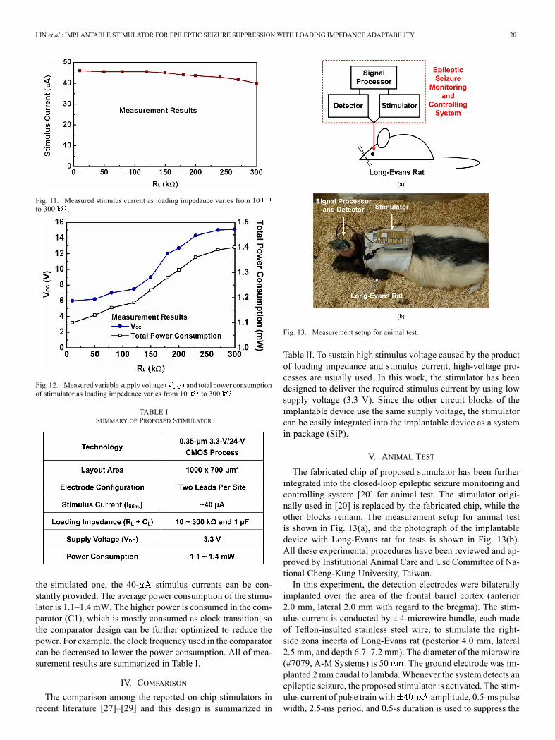
Fig. 13. Measurement setup for animal test.
Table II. To sustain high stimulus voltage caused by the productof loading impedance and stimulus current, high-voltage pro-cesses are usually used. In this work, the stimulator has beendesigned to deliver the required stimulus current by using lowsupply voltage (3.3 V). Since the other circuit blocks of theimplantable device use the same supply voltage, the stimulatorcan be easily integrated into the implantable device as a systemin package (SiP).
V. ANIMAL TEST
The fabricated chip of proposed stimulator has been furtherintegrated into the closed-loop epileptic seizure monitoring andcontrolling system [20] for animal test. The stimulator origi-nally used in [20] is replaced by the fabricated chip, while theother blocks remain. The measurement setup for animal testis shown in Fig. 13(a), and the photograph of the implantabledevice with Long-Evans rat for tests is shown in Fig. 13(b).All these experimental procedures have been reviewed and ap-proved by Institutional Animal Care and Use Committee of Na-tional Cheng-Kung University, Taiwan.In this experiment, the detection electrodes were bilaterally
implanted over the area of the frontal barrel cortex (anterior2.0 mm, lateral 2.0 mm with regard to the bregma). The stim-ulus current is conducted by a 4-microwire bundle, each madeof Teflon-insulted stainless steel wire, to stimulate the right-side zona incerta of Long-Evans rat (posterior 4.0 mm, lateral2.5 mm, and depth 6.7–7.2 mm). The diameter of the microwire(#7079, A-M Systems) is 50 . The ground electrode was im-planted 2mm caudal to lambda.Whenever the system detects anepileptic seizure, the proposed stimulator is activated. The stim-ulus current of pulse train with amplitude, 0.5-ms pulsewidth, 2.5-ms period, and 0.5-s duration is used to suppress the

202 IEEE TRANSACTIONS ON BIOMEDICAL CIRCUITS AND SYSTEMS, VOL. 7, NO. 2, APRIL 2013
TABLE IICOMPARISON AMONG CURRENT STIMULATORS IN RECENT LITERATURE
Fig. 14. Experimental results on EEG signals of Long-Evans rat (a) withoutstimulation, and (b) with stimulation.
epileptic seizure of Long-Evans rat. The injected charge densityis . The other microwire with wider diametercan also be used to decrease the charge density, since the pro-posed stimulator has considered the loading impedance adapt-ability.One Long-Evans rat with spontaneous absence epileptic dis-
charges is demonstrated in Fig. 14. The electroencephalography(EEG) signals of long-Evans rat without and with applyingthe stimulation are shown in Fig. 14(a) and (b), respectively.Each experiment is conducted for 10 minutes. In Fig. 14(a),the epileptic discharges are observed during 3.5–12 s. Whenthe seizure controller is applied in Fig. 14(b), the seizure isdetected during 3.5–5.5 s. Upon the detection of the seizure,the intensive and rapidly brain activities are suppressed by
the stimulation at . At this measurement, the loadingimpedance of stimulator is .According to the experiment results, the functionalities of the
proposed stimulator in the closed-loop epileptic seizure moni-toring and controlling system have been successfully verified.
VI. CONCLUSION
Design of bi-phasic stimulator for epileptic seizure suppres-sion with loading impedance adaptability is proposed in the0.35- 3.3-V/24-V CMOS process. The stimulator consists ofthe high voltage generator, output driver, adaptor, and switches.With adaptive loading consideration, the adaptor is used to de-tect the loading impedance, and the high voltage generator isable to adjust the suitable level of operating voltage. Whilethe loading impedance varies from 10 to 300 , the pro-posed stimulator can constantly deliver 40- stimulus current.The power consumption of this work is only 1.1 mW–1.4 mW.The stimulator is successfully integrated into the closed-loopepileptic seizure monitoring and controlling system for animaltests to verify its performances.
ACKNOWLEDGMENT
The authors would like to thank Prof. F.-Z. Shaw,Prof. S.-F. Liang, and their research groups at NationalCheng-Kung University, Taiwan, for their great help withanimal testing; and Prof. C.-Y. Wu, Prof. W.-T. Liu,Prof. J.-C. Chiou, Prof. H. Chiueh, Prof. C.-H. Yang,Dr. Y.-L. Hsin, and the research groups at the Biomedical Elec-tronics Translational Research Center, National Chiao-TungUniversity, Taiwan, for their valuable suggestions during circuitdesign. The authors would also like to thank the Editor and hisreviewers for their valuable suggestions to improve this paper.
REFERENCES[1] M. Leonardi and T. Ustun, “The global burden of epilepsy,” Epilepsia,
vol. 43, no. 6, pp. 21–25, Jul. 2002.[2] J. Burneo, J. Tellez-Zenteno, and S. Wiebe, “Understanding the burden
of epilepsy in Latin America: A systematic review of its prevalence andincidence,” Epilepsy Res., vol. 66, no. 1–3, pp. 63–74, Aug. 2005.

LIN et al.: IMPLANTABLE STIMULATOR FOR EPILEPTIC SEIZURE SUPPRESSION WITH LOADING IMPEDANCE ADAPTABILITY 203
[3] P. Hese, J. Martens, L. Waterschoot, P. Boon, and I. Lemahieu, “Au-tomatic detection of spike and wave discharges in the EEG of geneticabsence epilepsy rats from Strasbourg,” IEEE Trans. Biomed. Eng.,vol. 56, no. 3, pp. 706–717, Mar. 2009.
[4] E. Reynolds and M. Trimble, “Epilepsy, psychiatry, and neurology,”Epilepsia, vol. 50, no. 3, pp. 50–55, Mar. 2009.
[5] F. Bartolomei, P. Chauvel, and F.Wendling, “Epileptogenicity of brainstructures in human temporal lobe epilepsy: A quantified study fromintracerebral EEG,” Brain, vol. 131, no. 7, pp. 1818–1830, Jul. 2008.
[6] E. Perucca and T. Tomson, “The pharmacological treatment of epilepsyin adults,” Lancet Neurology, vol. 10, no. 5, pp. 446–456, May 2011.
[7] F. Andersohn, R. Schade, S. Willich, and E. Garbe, “Use ofantiepileptic drugs in epilepsy and the risk of self-harm or sui-cidal behavior,” Neurology, vol. 75, no. 4, pp. 335–340, Jul. 2010.
[8] C. Landmark and S. Johannessen, “Pharmacological management ofepilepsy: Recent advances and future prospects,” Drugs, vol. 68, no.14, pp. 1925–1939, Jan. 2008.
[9] P. Kwan and M. Brodie, “Early identification of refractory epilepsy,”New Eng. J. Med., vol. 342, no. 5, pp. 314–319, Feb. 2000.
[10] D. Binder,M. Podlogar, H. Clusmann, C. Bien, H. Urbach, J. Schramm,and T. Kral, “Surgical treatment of parietal lobe epilepsy,” J. Neuro-surg., vol. 110, pp. 1170–1178, Jun. 2009.
[11] J. Engel, “Surgical treatment for epilepsy: Too little, too late?,” J. Amer.Med. Assoc., vol. 300, no. 21, pp. 2548–2550, Dec. 2008.
[12] J. Langfitt and S. Wiebe, “Early surgical treatment for epilepsy,” Cur-rent Opin. Neurology, vol. 21, no. 2, pp. 179–183, Apr. 2008.
[13] G. Mathern, “Challenges in the surgical treatment of epilepsy patientswith cortical dysplasia,” Epilepsia, vol. 50, no. 9, pp. 45–50, Oct. 2009.
[14] S. Noachtar and I. Borggraefe, “Epilepsy surgery: A critical review,”Epilepsy Behav., vol. 15, no. 1, pp. 66–72, May 2009.
[15] W. Theodore and R. Fisher, “Brain stimulation for epilepsy,” LancetNeurology, vol. 2, no. 3, pp. 111–118, Jan. 2004.
[16] W. Stacey and B. Litt, “Technology insight: Neuroengineering andepilepsy—Designing devices for seizure control,” Nature Clin. Prac.Neurology, vol. 4, pp. 190–201, Feb. 2008.
[17] A. Milby, C. Halpern, and G. Baltuch, “Vagus nerve stimulation forepilepsy and depression,” Neurotherap., vol. 5, no. 1, pp. 75–85, Jan.2008.
[18] K. Taber, R. Hurley, and S. Yudofsky, “Diagnosis and treatment ofneuropsychiatric disorders,” Annu. Rev. Med., vol. 61, pp. 121–133,Feb. 2010.
[19] J. Sebeo, S. Deiner, R. Alterman, and I. Osborn, “Anesthesia for pedi-atric deep brain stimulation,” in Anesthesiol. Res. Prac.. : , 2010.
[20] C. Young, S. Liang, D. Chang, Y. Liao, F. Shaw, and C. Hsieh, “Aportable wireless online closed-loop seizure controller in freely movingrats,” IEEE Trans. Instrum. Meas., vol. 60, no. 2, pp. 513–521, Feb.2011.
[21] M. Salam, M. Sawan, and D. Nguyen, “A novel low-power-im-plantable epileptic seizure-onset detector,” IEEE Trans. Biomed.Circuits Syst., vol. 5, no. 6, pp. 568–578, Dec. 2011.
[22] M. Safi-Harb, M. Salam, D. Nguyen, and M. Sawan, “An implantableseizure-onset detector based on a dual-path single-window count-basedtechnique for closed-loop applications,” IEEE J. Emerg. Sel. TopicsCircuits Syst., vol. 1, no. 4, pp. 603–612, Dec. 2011.
[23] J. Coulombe, M. Sawan, and J. Gervais, “A highly flexible system formicrostimulation of the visual cortex: Design and implementation,”IEEE Trans. Biomed. Circuits Syst., vol. 1, no. 4, pp. 258–269, Dec.2007.
[24] E. Lee, “High-voltage tolerant stimulation monitoring circuit in con-ventional CMOS process,” in Proc. IEEE Custom Integrated CircuitsConf., 2009, pp. 93–96.
[25] M.-D. Ker, W.-L. Chen, and C.-Y. Lin, “Adaptable stimulus driver forepileptic seizure suppression,” in Proc. IEEE Int. Conf. Integrated Cir-cuit Design and Technology, 2011.
[26] M. Sivaprakasam,W. Liu, G.Wang, J.Weiland, andM.Humayun, “Ar-chitecture tradeoffs in high-density microstimulators for retinal pros-thesis,” IEEE Trans. Circuits Syst. I, Reg. Papers, vol. 52, no. 12, pp.2629–2641, Dec. 2005.
[27] S. Kelly and J. Wyatt, “A power-efficient neural tissue stimulator withenergy recovery,” IEEE Trans. Biomed. Circuits Syst., vol. 5, no. 1, pp.20–29, Feb. 2011.
[28] S. Ethier and M. Sawan, “Exponential current pulse generation forefficient very high-impedance multisite stimulation,” IEEE Trans.Biomed. Circuits Syst., vol. 5, no. 1, pp. 30–38, Feb. 2011.
[29] M.-D. Ker, C.-Y. Lin, and W.-L. Chen, “Stimulus driver for epilepsyseizure suppression with adaptive loading impedance,” J. Neural Eng.,vol. 8, no. 6, Dec. 2011.
[30] Y. Chang, C. Wang, and C. Wang, “A 8-bit 500-KS/s low power SARADC for bio-medical application,” in Proc. IEEE Asian Solid-StateCircuits Conf., 2007, pp. 228–231.
[31] M.-D. Ker, S.-L. Chen, and C.-S. Tsai, “Design of charge pump cir-cuit with consideration of gate oxide reliability in low-voltage CMOSprocess,” IEEE J. Solid-State Circuits, vol. 41, no. 5, pp. 1100–1107,May 2006.
[32] M. Porter, P. Gerrish, L. Tyler, S. Murray, R. Mauriello, F. Soto,G. Phetteplace, and S. Hareland, “Reliability considerations for im-plantable medical ICs,” in Proc. IEEE Int. Reliability Physics Symp.,2008, pp. 516–523.
[33] G. Palumbo, D. Pappalardo, and M. Gaibotti, “Charge-pump circuits:Power-consumption optimization,” IEEE Trans. Circuits Syst. I,Fundam. Theory Appl., vol. 49, no. 11, pp. 1535–1542, Nov. 2002.
Chun-Yu Lin (S’06–M’09) received the B.S. degreefrom the Department of Electronics Engineering andthe Ph.D. degree from the Institute of Electronics,National Chiao-Tung University, Hsinchu, Taiwan,in 2006 and 2009, respectively.Since 2009, he has been a Postdoctoral Researcher
of National Chiao-Tung University. His current re-search interests include ESD protection designs andbiomimetic circuit designs. Since 2010, he has alsoserved as the Secretary-General of the Taiwan ESDAssociation.
Wei-Ling Chen received the M.S. degree fromthe Institute of Electronics, National Chiao-TungUniversity, Hsinchu, Taiwan, in 2010. Since 2010,he has served in the military for obligatory militaryservice in Taiwan.
Ming-Dou Ker (S’92–M’94–SM’97–F’08) receivedthe Ph.D. degree from the Institute of Electronics,National Chiao-Tung University, Hsinchu, Taiwan,in 1993.He worked as the Department Manager with the
VLSI Design Division, Computer and Communica-tion Research Laboratories, Industrial TechnologyResearch Institute (ITRI), Hsinchu, Taiwan. Since2004, he has been a Full Professor with the De-partment of Electronics Engineering, NationalChiao-Tung University. During 2008–2011, he
was rotated to be Chair Professor and Vice President of I-Shou University,Kaohsiung, Taiwan. Now, he has been the Distinguished Professor in theDepartment of Electronics Engineering, National Chiao-Tung University. Heserved as the Executive Director of National Science and Technology Programon System-on-Chip (NSoC) in Taiwan during 2010–2011; and currently asthe Executive Director of National Science and Technology Program on NanoTechnology (NPNT) in Taiwan (2011–2014). In the technical field of reliabilityand quality design for microelectronic circuits and systems, he has publishedover 450 technical papers in international journals and conferences. He hasproposed many solutions to improve the reliability and quality of integratedcircuits, which have been granted with hundreds of U.S. patents and Taiwanpatents. He had been invited to teach and/or to consult the reliability and qualitydesign for integrated circuits by hundreds of design houses and semiconductorcompanies in the worldwide IC industry. His current research interests includereliability and quality design for nanoelectronics and gigascale systems,circuit-related reliability issue, as well as the biomimetic circuits and systemsfor intelligent prosthesis.Dr. Ker has served as a member of the Technical Program Committee and the
Session Chair of numerous international conferences for many years. He servedas the Associate Editor for the IEEE TRANSACTIONS ON VERY LARGE SCALEINTEGRATION SYSTEMS, 2006–2007. He was selected as the Distinguished Lec-turer in the IEEE Circuits and Systems Society (2006–2007) and in the IEEEElectron Devices Society (2008–present). He was the Founding President ofTaiwan ESD Association. In 2012, he started serving as the Editor of IEEETRANSACTIONS ON DEVICE AND MATERIALS RELIABILITY.