1742 IEEE TRANSACTIONS ON COMMUNICATIONS, VOL. 62, NO. … · 1742 IEEE TRANSACTIONS ON...
13
1742 IEEE TRANSACTIONS ON COMMUNICATIONS, VOL. 62, NO. 5, MAY 2014 Femtosecond-Long Pulse-Based Modulation for Terahertz Band Communication in Nanonetworks Josep Miquel Jornet, Member, IEEE, and Ian F. Akyildiz, Fellow, IEEE Abstract—Nanonetworks consist of nano-sized communicat- ing devices which are able to perform simple tasks at the nanoscale. Nanonetworks are the enabling technology of long- awaited applications such as advanced health monitoring systems or high-performance distributed nano-computing architectures. The peculiarities of novel plasmonic nano-transceivers and nano- antennas, which operate in the Terahertz Band (0.1-10 THz), require the development of tailored communication schemes for nanonetworks. In this paper, a modulation and channel access scheme for nanonetworks in the Terahertz Band is developed. The proposed technique is based on the transmission of one- hundred-femtosecond-long pulses by following an asymmetric On-Off Keying modulation Spread in Time (TS-OOK). The performance of TS-OOK is evaluated in terms of the achievable information rate in the single-user and the multi-user cases. An accurate Terahertz Band channel model, validated by COMSOL simulation, is used, and novel stochastic models for the molecular absorption noise in the Terahertz Band and for the multi-user interference in TS-OOK are developed. The results show that the proposed modulation can support a very large number of nano-devices simultaneously transmitting at multiple Gigabits- per-second and up to Terabits-per-second, depending on the modulation parameters and the network conditions. Index Terms—Nanonetworks, terahertz band, pulse-based communication, modulation. I. I NTRODUCTION N ANOTECHNOLOGY is providing a new set of tools to the engineering community to design and manufacture nanoscale components, able to perform only specific tasks at the nanoscale, such as computing, data storing, sensing and actuation. The integration of several of these nano-components into a single entity will result in autonomous nano-devices. By means of communication, these nano-devices will be able to achieve complex tasks in a distributed manner. The resulting nanonetworks will enable new applications of nanotechnology in the biomedical, environmental and military fields. One of the early applications of nanonetworks is in the field of nanosensing [2]. Nanosensors are nano-devices that take advantage of nanomaterials to detect new types of events at the nanoscale. For example, they can detect chemical compounds Manuscript received May 30, 2013; revised November 4, 2013 and February 19, 2014. The editor coordinating the review of this paper and approving it for publication was M. Buehrer. This work was supported by the U.S. National Science Foundation (NSF) under Grant No. CCF-1349828. J. M. Jornet is with the Department of Electrical Engineering, University at Buffalo, The State University of New York, NY 14260, USA (e-mail: [email protected]). I. F. Akyildiz is with the Broadband Wireless Networking Laboratory, School of Electrical and Computer Engineering, Georgia Institute of Tech- nology, Atlanta, GA 30332, USA (e-mail: [email protected]). A preliminary version of this work was presented in [1]. Digital Object Identifier 10.1109/TCOMM.2014.033014.130403 in very low concentrations (even a single molecule), and virus or harmful bacteria in very small populations. The size of an individual nanosensor is in the order of a few cubic micrometers, but their sensing range is limited to a few cubic micrometers as well. By means of communication, nanosen- sors will be able to transmit their information in a multi-hop fashion to a common sink. The resulting Wireless NanoSensor Networks (WNSNs) can be embedded for example in the fabric of our clothing to enable advanced health monitoring systems. Another application of nanonetworks is in the area of Wireless Network on Chip (WNoC) [3]. For example, wireless unicast, multicast and broadcast communication among nano- processors can drastically change the design principles of high-performance distributed computer architectures. The communication requirements of nanonetworks widely change across applications. For example, in WNSNs, very high node densities, in the order of hundreds of nanosensors per square millimeter, are needed to overcome the limited sensing range of individual devices. In addition, different type of nanosensors might be interleaved to detect different types of chemical compounds, which results in up to thousands of nano-devices per square millimter. With an individual response time of multiple microseconds [2], the aggregated throughput could reach multiple Gigabits per second (Gbps). When it comes to WNoC, the processing speed of an individual core and the total number of cores determines the aggregated throughput. From [3], data rates in the order of hundreds of Gbps per core are common, and multi-core architectures with tens and hundreds of cores already exist. While not all the cores might need wireless links all the time, peak data rates in the order of Terabits per second (Tbps) need to be supported. To date, the communication options for nano-devices are very limited. The miniaturization of a conventional metallic antenna to meet the size requirements of the nano-devices would impose the use of very high operating frequencies (hundreds of Terahertz). The available transmission bandwidth increases with the antenna resonant frequency, but so does the propagation loss. Due to the expectedly very limited power of nano-devices, the feasibility of nanonetworks would be compromised if this approach were followed. Alternatively, graphene, i.e., a one-atom-thick layer of carbon atoms in a honeycomb crystal lattice [4], has been proposed as the building material of novel plasmonic nano-antennas [5], [6]. These can efficiently operate at Terahertz Band frequencies (0.1-10 THz) [7], [8], [9], by exploiting the behavior of Surface Plasmon Polariton (SPP) waves. Nano-antennas are just tens of nanometers wide and few micrometers long, and can potentially be easily integrated in nano-devices. 0090-6778/14$31.00 c 2014 IEEE
Transcript of 1742 IEEE TRANSACTIONS ON COMMUNICATIONS, VOL. 62, NO. … · 1742 IEEE TRANSACTIONS ON...

1742 IEEE TRANSACTIONS ON COMMUNICATIONS, VOL. 62, NO. 5, MAY 2014
Femtosecond-Long Pulse-Based Modulation forTerahertz Band Communication in Nanonetworks
Josep Miquel Jornet, Member, IEEE, and Ian F. Akyildiz, Fellow, IEEE
Abstract—Nanonetworks consist of nano-sized communicat-ing devices which are able to perform simple tasks at thenanoscale. Nanonetworks are the enabling technology of long-awaited applications such as advanced health monitoring systemsor high-performance distributed nano-computing architectures.The peculiarities of novel plasmonic nano-transceivers and nano-antennas, which operate in the Terahertz Band (0.1-10 THz),require the development of tailored communication schemes fornanonetworks. In this paper, a modulation and channel accessscheme for nanonetworks in the Terahertz Band is developed.The proposed technique is based on the transmission of one-hundred-femtosecond-long pulses by following an asymmetricOn-Off Keying modulation Spread in Time (TS-OOK). Theperformance of TS-OOK is evaluated in terms of the achievableinformation rate in the single-user and the multi-user cases. Anaccurate Terahertz Band channel model, validated by COMSOLsimulation, is used, and novel stochastic models for the molecularabsorption noise in the Terahertz Band and for the multi-userinterference in TS-OOK are developed. The results show thatthe proposed modulation can support a very large number ofnano-devices simultaneously transmitting at multiple Gigabits-per-second and up to Terabits-per-second, depending on themodulation parameters and the network conditions.
Index Terms—Nanonetworks, terahertz band, pulse-basedcommunication, modulation.
I. INTRODUCTION
NANOTECHNOLOGY is providing a new set of tools tothe engineering community to design and manufacture
nanoscale components, able to perform only specific tasks atthe nanoscale, such as computing, data storing, sensing andactuation. The integration of several of these nano-componentsinto a single entity will result in autonomous nano-devices. Bymeans of communication, these nano-devices will be able toachieve complex tasks in a distributed manner. The resultingnanonetworks will enable new applications of nanotechnologyin the biomedical, environmental and military fields.
One of the early applications of nanonetworks is in the fieldof nanosensing [2]. Nanosensors are nano-devices that takeadvantage of nanomaterials to detect new types of events at thenanoscale. For example, they can detect chemical compounds
Manuscript received May 30, 2013; revised November 4, 2013 and February19, 2014. The editor coordinating the review of this paper and approving itfor publication was M. Buehrer.
This work was supported by the U.S. National Science Foundation (NSF)under Grant No. CCF-1349828.
J. M. Jornet is with the Department of Electrical Engineering, Universityat Buffalo, The State University of New York, NY 14260, USA (e-mail:[email protected]).
I. F. Akyildiz is with the Broadband Wireless Networking Laboratory,School of Electrical and Computer Engineering, Georgia Institute of Tech-nology, Atlanta, GA 30332, USA (e-mail: [email protected]).
A preliminary version of this work was presented in [1].Digital Object Identifier 10.1109/TCOMM.2014.033014.130403
in very low concentrations (even a single molecule), andvirus or harmful bacteria in very small populations. The sizeof an individual nanosensor is in the order of a few cubicmicrometers, but their sensing range is limited to a few cubicmicrometers as well. By means of communication, nanosen-sors will be able to transmit their information in a multi-hopfashion to a common sink. The resulting Wireless NanoSensorNetworks (WNSNs) can be embedded for example in thefabric of our clothing to enable advanced health monitoringsystems. Another application of nanonetworks is in the area ofWireless Network on Chip (WNoC) [3]. For example, wirelessunicast, multicast and broadcast communication among nano-processors can drastically change the design principles ofhigh-performance distributed computer architectures.
The communication requirements of nanonetworks widelychange across applications. For example, in WNSNs, veryhigh node densities, in the order of hundreds of nanosensorsper square millimeter, are needed to overcome the limitedsensing range of individual devices. In addition, different typeof nanosensors might be interleaved to detect different typesof chemical compounds, which results in up to thousands ofnano-devices per square millimter. With an individual responsetime of multiple microseconds [2], the aggregated throughputcould reach multiple Gigabits per second (Gbps). When itcomes to WNoC, the processing speed of an individual coreand the total number of cores determines the aggregatedthroughput. From [3], data rates in the order of hundreds ofGbps per core are common, and multi-core architectures withtens and hundreds of cores already exist. While not all thecores might need wireless links all the time, peak data rates inthe order of Terabits per second (Tbps) need to be supported.
To date, the communication options for nano-devices arevery limited. The miniaturization of a conventional metallicantenna to meet the size requirements of the nano-deviceswould impose the use of very high operating frequencies(hundreds of Terahertz). The available transmission bandwidthincreases with the antenna resonant frequency, but so does thepropagation loss. Due to the expectedly very limited powerof nano-devices, the feasibility of nanonetworks would becompromised if this approach were followed. Alternatively,graphene, i.e., a one-atom-thick layer of carbon atoms ina honeycomb crystal lattice [4], has been proposed as thebuilding material of novel plasmonic nano-antennas [5], [6].These can efficiently operate at Terahertz Band frequencies(0.1-10 THz) [7], [8], [9], by exploiting the behavior ofSurface Plasmon Polariton (SPP) waves. Nano-antennas arejust tens of nanometers wide and few micrometers long, andcan potentially be easily integrated in nano-devices.
0090-6778/14$31.00 c© 2014 IEEE

JORNET and AKYILDIZ: FEMTOSECOND-LONG PULSE-BASED MODULATION FOR TERAHERTZ BAND COMMUNICATION IN NANONETWORKS 1743
In this same direction, compact Terahertz Band plasmonicsignal generators and detectors are being developed [10], [11].Contrary to classical Terahertz Band radiation sources, whichusually require high power bulky devices and sophisticatedcooling systems [12], solid-state Terahertz Band emitters canelectronically excite SPP waves at Terahertz Band frequenciesfrom a compact structure built on a High Electron MobilityTransistor (HEMT) based on semiconductor materials. How-ever, for the time being, at room temperature, only very shortpulses, just a hundred femtosecond long, can be generated,with a power of just a few μW per pulse. While this mightnot be enough for long range Terahertz Band communication,it opens the door to communication in nanonetworks.
The lack of nanoscale transceivers able to generate a carriersignal at Terahertz Band frequencies limits the feasibility ofcarrier-based modulations, and motivates the use of pulse-based communication schemes in nanonetworks. When size isnot a constraint, carrier-based modulations can still be used, asshown in [13], [14], [15]. Pulse-based modulations have beenwidely used in very high speed communications systems suchas Impulse Radio Ultra-Wide-Band (IR-UWB) [16] and free-space optical (FSO) systems [17]. However, the peculiaritiesof nano-transceivers and nano-antennas and the phenomenathat affect the propagation of these very short pulses in theTerahertz Band requires a revision of common assumptions inpulse-based communications.
In this paper, we propose and analyze the performanceof a pulse-based modulation and channel access scheme fornanonetworks in the Terahertz Band, which is based onthe transmission of one-hundred-femtosecond-long pulses byfollowing an asymmetric On-Off Keying modulation Spreadin Time (TS-OOK). This scheme is tailored to the expectedcapabilities of Terahertz Band signal generators and detectors,and exploits the peculiarities of the Terahertz Band channel.
The main contributions of this paper are summarized asfollows. First, in Sec. II, we revise the state of the art andhighlight the peculiarities of Terahertz Band nanoscale signalgenerators and detectors, the impact of the nano-antenna in thetransmission and in reception, as well as the channel effectsand propagation phenomena in the Terahertz Band.
Second, in Sec. III, we propose TS-OOK as a modulationand channel access scheme for nanonetworks in the TerahertzBand and briefly describe its functioning in the single-userand the multi-user cases. Third, we analytically model theperformance of TS-OOK in an interference-free scenario.For this, we develop a new stochastic model of noise inthe Terahertz Band, and we use this model to analyze themaximum achievable information rate. The details on the noisemodel and information rate analysis are presented in Sec. IV.
Fourth, we extend our analysis on the performance of TS-OOK to the multi-user case. For this, we develop a stochasticmodel of multi-user interference in pulse-based communica-tion in the Terahertz Band. This model considers a uniformdistribution of nano-devices in space, which communicate inan asynchronous manner in an ad-hoc fashion and withouta central coordinator. We then use this model to analyticallyinvestigate the achievable information rate in the presence ofmulti-user interference. Our analysis is treated in Sec. V.
Finally, we use COMSOL Multi-physics [18] to validate our
models by mean of time-domain electromagnetic simulations,and we numerically investigate the achievable information ratefor the two cases under study. Our results show that, despiteits simplicity, when using TS-OOK, nanonetworks can supporta very large number of nano-devices simultaneously trans-mitting at very high bit-rates, given that asymmetric sourceprobability distributions are used to prioritize the transmissionof silence. The achievable rates range from a few Gbps to afew Tbps, depending on the TS-OOK parameters and nano-device density. The details on our simulation and numericalanalysis are presented in Sec. VI. We conclude the paper inSec. VII.
II. TERAHERTZ BAND PULSE-BASED SYSTEMS
A. Signal Generation
Terahertz Band signal generators for communication amongnano-devices must be i) compact, i.e., up to several hundredsof square nanometers or a few square micrometers at most;ii) fast, i.e., able to support modulation bandwidths of at leastseveral GHz; iii) energy-efficient, and iv) preferably tunable.
Several technologies are being considered for the generationof Terahertz Band signals. For the time being, monolithic inte-grated circuits based on Silicon [19], Silicon Germanium [20],Indium Phosphide [21] and Gallium Nitride [22], have beendemonstrated at frequencies between 0.1 and 1 THz. Forhigher frequency operation, photonic devices and, in partic-ular, Quantum Cascade Lasers (QCLs) [12], are commonlyutilized. QCLs can operate at frequencies above a few THzand can generate an average power up to a few mW. However,the need of an external laser for optical electron pumpingand their size (at least several square millimeters) hamper theapplication of QCLs for communication in nanonetworks.
More recently, compact signal generators are being devel-oped by using a single HEMT based on III-V compound semi-conductors (e.g., Gallium Nitride) as well as graphene [10],[11]. In particular, it has been shown that SPP waves atTerahertz Band frequencies can be excited in the channel ofa HEMT with nanometric gate length by means of eitherelectrical or optical pumping. When a voltage is appliedbetween the drain and the source of the HEMT, electronsare accelerated from the source to the drain. This suddenmovement of electrons results in the excitation of a SPP wavedue to the energy band-structure of the building material ofthe HEMT. At room temperature, however, the SPP waves areoverdamped and only very short broadband incoherent SPPwaves are generated. These resemble very short pulses, justseveral tens of femtoseconds long.
In our analysis, we model the generated signals as one-hundred-femtosecond-long Gaussian pulses. These type ofpulses are already being used in several applications suchas Terahertz imaging and biological spectroscopy [23]. Thep.s.d. of these pulses has its main frequency components in theTerahertz Band. Pulses with a peak power of a few μW, i.e.,with equivalent energies of just a few aJ (10−18J), have beenreported in the related literature [11]. An additional technologylimitation at the generator is that pulses cannot be transmittedin a burst, but due to the relaxation time of SPP waves in theHEMT channel, need to be spread in time. In our analysis,
1744 IEEE TRANSACTIONS ON COMMUNICATIONS, VOL. 62, NO. 5, MAY 2014
we consider the energy per pulse and the spreading betweenpulses as two technology parameters.
B. Signal Radiation
The resulting plasmonic signal can be then radiated by aTerahertz Band plasmonic nano-antenna, such as the designsproposed in [5], [6]. The radiated waveform depends on theantenna behavior in transmission. Contrary to classical narrow-band communication systems, and in-line with UWB systems,the antenna response cannot be modeled with a single gain,but the entire frequency response or the antenna impulseresponse are needed. Independently of the particular antennadesign, from [24], [25], the radiated electromagnetic field isproportional to the first time derivative of the current densityat the antenna surface. For this, we model the antenna impulseresponse in transmission hT
ant as:
hTant (t) =
∂
∂t
∫Jδ
|| (t, r′) dV ′, (1)
where t refers to time, V ′ stands for the volume occupied bythe antenna, Jδ
|| (in units of [1/m2s]) is the current distributionon the antenna due to an impulse input current δ (t) in thetransverse direction relative to the observation direction, andr′ = (x, y). The current distribution on the antenna Jδ
||depends on the particular antenna design, and usually it canonly be numerically obtained. At this stage, we keep ouranalysis general for any possible antenna. In our results, weutilize COMSOL Multi-physics to account for the impact of anelectric point dipole in transmission. More details are providedin Sec. VI.
C. Signal Propagation
The propagation of the radiated pulses is determined bythe Terahertz Band channel behavior. Existing channel modelsfor lower frequency bands cannot be utilized at TerahertzBand frequencies, because they do not capture the peculiaritiesof this frequency range, such as the impact of molecularabsorption on the signal propagation. In addition, the fewexisting Terahertz Band channel models [26], [27], [28] areaimed at characterizing only a fraction of the Terahertz Band(e.g., 300 GHz window) and usually over large propagationdistances (several meters). However, in light of the limitedtransmission power of nano-devices and the broadband natureof the generated signals, there is a need to model the entireTerahertz Band for distances much below one meter.
In this direction, we have recently developed a channelmodel for Terahertz Band communications [29]. The maindifference with other frequency bands comes from the molec-ular absorption loss. The absorption loss accounts for theattenuation that a propagating wave suffers because of molec-ular absorption, i.e., the process by which part of the waveenergy is converted into internal kinetic energy to some ofthe molecules which are found in the channel. This lossdepends on the signal frequency, the transmission distance andthe concentration and the mixture of molecules encounteredalong the path. As a result, the Terahertz Band channel ishighly frequency selective, specially when the concentrationof molecules or the transmission distance are increased.
From [29], the Terahertz Band channel frequency responseHc is given by
Hc (f, d) = Hspread (f, d)Habs (f, d) , (2)
where Hspread and Habs refer to the spreading loss and themolecular absorption loss, respectively, and are given by
Hspread (f, d) =
(1√4πd
)exp (−ı2πfd/c) (3)
Habs (f, d) = exp
(−1
2k (f) d
), (4)
where f stands for frequency, d stands for distance, and k isthe medium absorption coefficient, given by
k (f) =∑i
p
p0
TSTP
TQiσi (f) , (5)
where p refers to the system pressure in Kelvin, p0 is the ref-erence pressure (1 atm), TSTP is the temperature at standardpressure (273.15 K), Q is the number of molecules per volumeunit of gas i and σi is the absorption cross-section of gasi. More details on how to compute the molecular absorptioncross-section σ can be found in [29].
The channel impulse response hc is obtained by using theInverse Fourier transform
hc (t, d) = F−1 {Hc (f, d)} . (6)
This inverse Fourier Transform does not have an analyticalexpression. In our analysis, we will numerically compute thechannel time response. As we describe in Sec. VI, we useCOMSOL Multi-physics to validate this model by means ofextensive time-domain simulations. In addition, this model cansuccessfully reproduce existing measurements for the lowerrange of the Terahertz Band between 100 GHz and 1 THz,such as the values reported in [27].
There are additional propagation effects that might impactthe received signal, such as multi-path propagation. A multi-path model for the Terahertz Band needs to account forthe impact of molecular absorption, the reflection coefficientof common materials at Terahertz Band frequencies andthe impact of diffused scattering on rough surfaces [30],amongst others. The few multi-path channel models existingto date [28] are mainly focused on the 300 GHz window, anda complete model for the entire Terahertz Band does not exist.As a result, we do not account for multi-path in this work.
D. Signal Reception
The signal at the receiver depends on the antenna impulseresponse in reception. From [24], [25], this is proportionalto the time integral of the antenna impulse response intransmission. For this, we model the antenna impulse responsein reception hR
ant as:
hRant (t) =
∫ t
0
hTant (τ) dτ, (7)
where t refers to time and hTant is the antenna impulse response
in transmission, given by (1). As before, the antenna impulseresponse in reception depends on the particular antenna, andcan generally only numerically be obtained. In our results, we

JORNET and AKYILDIZ: FEMTOSECOND-LONG PULSE-BASED MODULATION FOR TERAHERTZ BAND COMMUNICATION IN NANONETWORKS 1745
utilize COMSOL Multi-physics to incorporate the impact ofan electric point dipole antenna in reception.
The system impulse response, which captures the impact ofthe antenna in transmission, the propagation effects, and theimpact of the antenna in reception, is finally given by:
h (t) = hTant (t) ∗ hc (t) ∗ hR
ant (t) . (8)
In classical narrow-band systems, the impact of the antenna intransmission and in reception is usually captured by taking intoaccount the following relation between the antenna directivityD and its effective area Aeff in reception:
Dλ2 = 4πAeff , (9)
where λ stands for the wavelength at the design centerfrequency of the system. It is relevant to note that both thedirectivity D and the effective area Aeff depend on thefrequency themselves, and thus, the utilization of the afore-mentioned expression would be a narrow-band approximation.We do not follow this approach, and model instead the antennaimpulse response in transmission and in reception numericallyin COMSOL.
E. Signal Detection
Many technologies are being considered for the detectionof Terahertz Band signals. Currently, the most developedsolutions rely on bolometers [31] and Schottky diodes [32].On the one hand, bolometric detectors are able to detect verylow power signals and have a high modulation bandwidth(up to a few GHz). However, their low performance at roomtemperature and their size pose a major constraint for the nano-devices. Similarly, the detection systems based on Schottkydiodes can operate at room temperature and exhibit a highmodulation bandwidth (up to 10 GHz), but their size limitstheir integration with the rest of the nano-transceiver.
Alternatively, the same HEMT-based structure discussed intransmission, has been proposed for the detection of TerahertzBand signals [10], [11]. The injection of a plasmonic current inthe channel of the HEMT results into electrons being pushedfrom the source to the drain. This effectively creates a voltagebetween the drain and the source. Recent works show howHEMT-based detectors provide excellent sensitivities with theintrinsic possibility of high-speed response (limited only bythe read-out electronics impedance).
Similarly as in transmission, at room temperature, HEMT-based detectors can only measure the amplitude of the receivedsignals, but not their phase. A sensitivity or noise equivalentpower as low as 10 fW/
√Hz has been reported in [33]. For
the time being, an accurate symbol detection model for one-hundred-femtosecond-long pulses is missing. A preliminaryversion of our ongoing work to develop a new symbol detec-tion model can be found in [34]. In order to separate the impactof the symbol detection scheme on the system performance,we will consider an ideal matched filter in our analysis.
III. TIME SPREAD ON-OFF KEYING
In this section, we describe the proposed communicationtechnique for nanonetworks, which serves both as a modula-tion scheme as well as a multiple access mechanism.
A. Modulation Definition
In light of the capabilities of nano-transceivers, we proposethe use of TS-OOK for communication among nano-devicesin the Terahertz Band. TS-OOK is based on the exchangeof one-hundred-femtosecond-long pulses among nano-devices.The functioning of this communication scheme is as follows:
• A logical “1” is transmitted by using a one-hundred-femtosecond-long pulse and a logical “0” is transmittedas silence, i.e., the nano-device remains silent when alogical zero is transmitted. As discussed above, solid-stateTerahertz Band transceivers are not expected to be able toaccurately control the shape or phase of the transmittedpulses and, thus, a simple OOK modulation is used. Toavoid the confusion between the transmission of silenceand the no transmission, initialization preambles andconstant-length packets can be used. After the detectionof the preamble, silence is considered a logical “0”.
• The time between transmissions is fixed and much longerthan the pulse duration. Due to the nano-transceiverlimitations above described, pulses or silences are nottransmitted in a burst, but spread in time as in IR-UWB.By fixing the time between consecutive transmissions,after an initialization preamble, a nano-device does notneed to continuously sense the channel, but it just waitsfor the next transmission. This scheme does not requiretight synchronization among nano-devices all the time,but only selected nano-devices will be synchronized afterthe detection of the initialization preamble.
Under this scheme, the signal transmitted by a nano-deviceu, suT is given by:
suT (t) =
K∑k=1
Aukp (t− kTs − τu) (10)
where K is the number of symbols per packet, Auk refers to
the amplitude of the k-th symbol transmitted by the nano-device u (either 0 or 1), p stands for a pulse with duration Tp,Ts refers to the time between consecutive transmissions, andτu is a random initial transmission delay. In general, the timebetween symbols is much longer than the time between pulses.Following the usual notation, we define β = Ts/Tp � 1.
The signal received by a nano-device j can be written as:
sjR (t) =
K∑k=1
Aukp (t− kTs − τu) ∗ hu,j (t) + nu,j
k (t) (11)
where hu,j is the system impulse response between the nano-devices u and j, in (8), and depends on the specific mediumconditions and the distance between the transmitter u and thereceiver j. nu,j
k stands for the noise affecting the transmissionof symbol k between u and j, described in Sec. IV-A.
B. Medium Sharing with TS-OOK
TS-OOK enables robust and concurrent communicationamong nano-devices. In the envisioned scenarios, nano-devices can start transmitting at any time without beingsynchronized or controlled by any type of network centralentity. However, due to the fact that the time between trans-missions Ts is much longer than the pulse duration Tp,
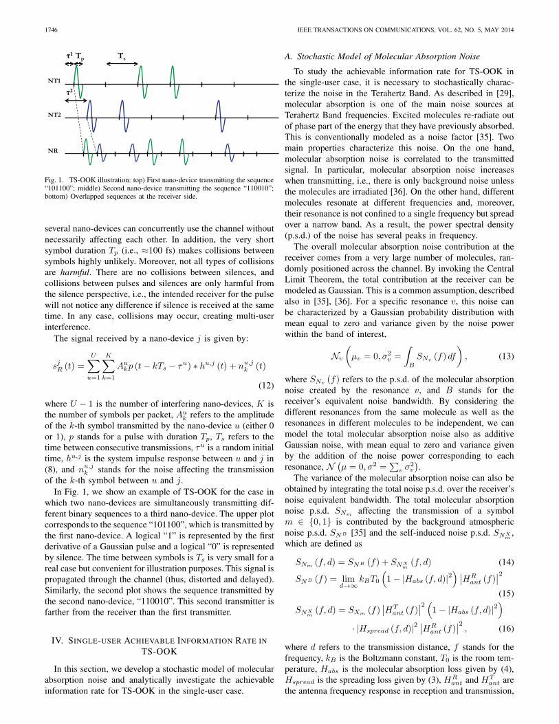
1746 IEEE TRANSACTIONS ON COMMUNICATIONS, VOL. 62, NO. 5, MAY 2014
NT2
NR
NT1
Tp Ts τ1
τ2
Fig. 1. TS-OOK illustration: top) First nano-device transmitting the sequence“101100”; middle) Second nano-device transmitting the sequence “110010”;bottom) Overlapped sequences at the receiver side.
several nano-devices can concurrently use the channel withoutnecessarily affecting each other. In addition, the very shortsymbol duration Tp (i.e., ≈100 fs) makes collisions betweensymbols highly unlikely. Moreover, not all types of collisionsare harmful. There are no collisions between silences, andcollisions between pulses and silences are only harmful fromthe silence perspective, i.e., the intended receiver for the pulsewill not notice any difference if silence is received at the sametime. In any case, collisions may occur, creating multi-userinterference.
The signal received by a nano-device j is given by:
sjR (t) =
U∑u=1
K∑k=1
Aukp (t− kTs − τu) ∗ hu,j (t) + nu,j
k (t)
(12)
where U − 1 is the number of interfering nano-devices, K isthe number of symbols per packet, Au
k refers to the amplitudeof the k-th symbol transmitted by the nano-device u (either 0or 1), p stands for a pulse with duration Tp, Ts refers to thetime between consecutive transmissions, τu is a random initialtime, hu,j is the system impulse response between u and j in(8), and nu,j
k stands for the noise affecting the transmissionof the k-th symbol between u and j.
In Fig. 1, we show an example of TS-OOK for the case inwhich two nano-devices are simultaneously transmitting dif-ferent binary sequences to a third nano-device. The upper plotcorresponds to the sequence “101100”, which is transmitted bythe first nano-device. A logical “1” is represented by the firstderivative of a Gaussian pulse and a logical “0” is representedby silence. The time between symbols is Ts is very small for areal case but convenient for illustration purposes. This signal ispropagated through the channel (thus, distorted and delayed).Similarly, the second plot shows the sequence transmitted bythe second nano-device, “110010”. This second transmitter isfarther from the receiver than the first transmitter.
IV. SINGLE-USER ACHIEVABLE INFORMATION RATE IN
TS-OOK
In this section, we develop a stochastic model of molecularabsorption noise and analytically investigate the achievableinformation rate for TS-OOK in the single-user case.
A. Stochastic Model of Molecular Absorption Noise
To study the achievable information rate for TS-OOK inthe single-user case, it is necessary to stochastically charac-terize the noise in the Terahertz Band. As described in [29],molecular absorption is one of the main noise sources atTerahertz Band frequencies. Excited molecules re-radiate outof phase part of the energy that they have previously absorbed.This is conventionally modeled as a noise factor [35]. Twomain properties characterize this noise. On the one hand,molecular absorption noise is correlated to the transmittedsignal. In particular, molecular absorption noise increaseswhen transmitting, i.e., there is only background noise unlessthe molecules are irradiated [36]. On the other hand, differentmolecules resonate at different frequencies and, moreover,their resonance is not confined to a single frequency but spreadover a narrow band. As a result, the power spectral density(p.s.d.) of the noise has several peaks in frequency.
The overall molecular absorption noise contribution at thereceiver comes from a very large number of molecules, ran-domly positioned across the channel. By invoking the CentralLimit Theorem, the total contribution at the receiver can bemodeled as Gaussian. This is a common assumption, describedalso in [35], [36]. For a specific resonance v, this noise canbe characterized by a Gaussian probability distribution withmean equal to zero and variance given by the noise powerwithin the band of interest,
Nv
(μv = 0, σ2
v =
∫B
SNv (f)df
), (13)
where SNv (f) refers to the p.s.d. of the molecular absorptionnoise created by the resonance v, and B stands for thereceiver’s equivalent noise bandwidth. By considering thedifferent resonances from the same molecule as well as theresonances in different molecules to be independent, we canmodel the total molecular absorption noise also as additiveGaussian noise, with mean equal to zero and variance givenby the addition of the noise power corresponding to eachresonance, N
(μ = 0, σ2 =
∑v σ
2v
).
The variance of the molecular absorption noise can also beobtained by integrating the total noise p.s.d. over the receiver’snoise equivalent bandwidth. The total molecular absorptionnoise p.s.d. SNm affecting the transmission of a symbolm ∈ {0, 1} is contributed by the background atmosphericnoise p.s.d. SNB [35] and the self-induced noise p.s.d. SNX
m,
which are defined as
SNm (f, d) = SNB (f) + SNXm(f, d) (14)
SNB (f) = limd→∞
kBT0
(1− |Habs (f, d)|2
) ∣∣HRant (f)
∣∣2(15)
SNXm(f, d) = SXm (f)
∣∣HTant (f)
∣∣2 (1− |Habs (f, d)|2)
· |Hspread (f, d)|2∣∣HR
ant (f)∣∣2 , (16)
where d refers to the transmission distance, f stands for thefrequency, kB is the Boltzmann constant, T0 is the room tem-perature, Habs is the molecular absorption loss given by (4),Hspread is the spreading loss given by (3), HR
ant and HTant are
the antenna frequency response in reception and transmission,

JORNET and AKYILDIZ: FEMTOSECOND-LONG PULSE-BASED MODULATION FOR TERAHERTZ BAND COMMUNICATION IN NANONETWORKS 1747
respectively, which are obtained as the Fourier transform of (7)and (1), and SXm is the p.s.d. of the transmitted signal.
The term SNB takes into account that the backgroundnoise is i) generated from molecules that radiate for beingat a temperature above 0 K, and ii) detected by an antennain reception. The term SNX
mtakes into account that the
induced noise is i) generated by the transmitted signal Xm,ii) spherically spread from the transmitting antenna, and iii)detected by an antenna in reception.
Finally, the total noise power at the receiver Nm when thesymbol m ∈ {0, 1} is transmitted is given by
Nm (d) =
∫B
SNm (f, d) |Hr (f)|2 df, (17)
where B is the receiver’s noise equivalent bandwidth and Hr
is the receiver’s frequency response described in Sec. II.In addition to the molecular absorption noise, there are other
noise sources that can affect the achievable information ratein the proposed scheme, such as the electronic noise at thereceiver. The noise factor at the receiver drastically dependson the specific device technology. However, a stochastic modelfor the electronic noise at the receiver is missing. In ouranalysis, we aim at obtaining an upper bound, independentof the transceiver technology. These results will be extendedas stochastic noise models for the receiver are developed.
B. Analytical Study of the Single-user Information Rate
The maximum achievable information rate in bit/symbolIRu−sym of a communication system for a specific modu-lation scheme is given by
IRu−sym = maxX
{H (X)−H (X |Y )} , (18)
where X refers to the source of information, Y refers to theoutput of the channel, H (X) refers to the entropy of thesource X , and H (X |Y ) stands for the conditional entropyof X given Y or the equivocation of the channel.
In our analysis, we consider the source of information X tobe discrete, and the output signal of the transmitter suT in (10),the channel response h in (8) and the molecular absorptionnoise n to be continuous. Under these considerations, thesource X can be modeled as a discrete binary random variable.
Therefore, the entropy of the source H (X) is given by:
H (X) = −1∑
m=0
pX (xm) log2 pX (xm), (19)
where pX (xm) refers to the probability of transmitting thesymbol m = {0, 1}, i.e., the probability to stay silent or totransmit a pulse, respectively.
The output Y of the channel can be modeled as a continuousrandom variable. In particular, the output of the transmitter isdistorted by the channel h, and corrupted by the molecularabsorption noise n. The only random component affecting thereceived signal is the molecular absorption noise.
By recalling the Mixed Bayes Rule and the Total ProbabilityTheorem [37], the equivocation H (X |Y ) can be written interms of the probability of the channel output Y given theinput xm, fY (Y |X = xm),
H (X |Y ) =
∫y
1∑m=0
fY (Y |X = xm) pX (xm)
· log2
⎛⎜⎜⎝
1∑n=0
fY (Y |X = xn) pX (xn)
fY (Y |X = xm) pX (xm)
⎞⎟⎟⎠ dy.
(20)
Based on the stochastic model of molecular absorptionnoise, the p.d.f. of the output of the system Y given the inputX = xm can be written as:
fY (Y |X = xm) =1√
2πNm
e−12
(y−am)2
Nm , (21)
where Nm stands for the total noise power associated to thetransmitted symbol xm and am refers to the amplitude of thereceived symbol, which is obtained by using the TerahertzBand system model described in Sec. II.
By combining (19), (20) and (21) in (18), the achievableinformation rate in bit/symbol can be written as (22). Finally,the maximum achievable information rate in bit/second isobtained by multiplying the rate in bit/symbol (22) by therate at which symbols are transmitted, R = 1/Ts = 1/(βTp),where Ts is the time between symbols, Tp is the pulse length,and β is the ratio between them. If we assume that theBTp ≈ 1, where B stands for the channel bandwidth, the
IRu−sym = maxX
{−
1∑m=0
pX (xm) log2 pX (xm)−∫ 1∑
m=0
1√2πNm
e−12
(y−am)2
Nm pX (xm)
· log2
(1∑
n=0
pX (xn)
pX (xm)
√Nm
Nne−
12
(y−an)2
Nn+ 1
2(y−am)2
Nm
)dy
}
= − maxpX(x0)
{∫pX (x0)√2πN0
e−12
y2
N0 log2
(pX (x0)
(1 +
1− pX (x0)
pX (x0)
√N0
N1e−
12
y2
N0+ 1
2
(y−a1)2
N1
))
+1− pX (x0)√
2πN1
e−12
(y−a1)2
N1 log2
((1− pX (x0))
(1 +
pX (x0)
1− pX (x0)
√N1
N0e−
12
(y−a1)2
N1+ 1
2y2
N0
))dy
}.
(22)

1748 IEEE TRANSACTIONS ON COMMUNICATIONS, VOL. 62, NO. 5, MAY 2014
rate in bit/second is given by:
IRu =B
βIRu−sym. (23)
If β = 1, i.e., all the symbols (pulses or silences) aretransmitted in a burst, and the maximum rate per nano-deviceis achieved, provided that the incoming information rate andthe read-out rate to and from the nano-transceiver can matchthe channel rate. By increasing β, the single-user rate isreduced, but the requirements on the transceiver are greatlyrelaxed, as we explained in Sec. II. Analytically solving themaximum information rate expression given by (22) is notfeasible. Instead, we numerically investigate it in Sec. VI.
V. MULTI-USER ACHIEVABLE INFORMATION RATE
IN TS-OOK
In this section, we develop a stochastic model for inter-ference in TS-OOK and formulate the multi-user achievableinformation rate analytically.
A. Stochastic Model of Multi-user Interference in TS-OOK
Multi-user interference in TS-OOK occurs when symbolsfrom different nano-devices reach the receiver at the sametime and overlap. Without loss of generality, we focus on thesymbols transmitted by the nano-device number 1. Then, theinterference I at the receiver j during the detection of a symbolfrom node number 1 is given by:
I =
U∑u=2
Au (p ∗ h)u,j (T u1 ) + nu,j (T u
1 ) , (24)
where U refers to the total number of nano-devices, Au isthe amplitude of the symbol transmitted by the nano-device u(either one or zero), (p ∗ h)u,j stands for the transmitted pulseconvoluted with the system impulse response between nano-devices u and j, T u
1 is the time difference at the receiverside between the transmissions from nano-devices 1 and u,and nu,j is the absorption noise created at the receiver by thetransmissions from the nano-device u.
Many stochastic models of interference have been devel-oped to date. For example, an extensive review of the existingmodels can be found in [38], [39], [40]. However, these modelsdo not capture the peculiarities of the Terahertz Band channel,such as the molecular absorption loss and the additionalmolecular absorption noise created by interfering nodes. Inorder to provide a stochastic characterization of the interfer-ence in TS-OOK, we make the following considerations:
1) Nano-devices are not controlled by a central entity, butthey communicate in an uncoordinated fashion.
2) Transmissions from different nano-devices are indepen-dent and follow the same source probability X .
3) The random initial time τ in (10) is uniformly dis-tributed.
4) Nano-devices are uniformly distributed in space, thus,the propagation delay between any pair of nano-devicesis also uniformly distributed in time.
5) Collisions between silences are not harmful. Collisionsbetween pulses and silences are only harmful from thesilence perspective.
Under these considerations, the time difference at the re-ceiver side between the transmissions from the nano-devices1 and u, T u
1 , can be modeled as a uniform random variableover [0, Ts]. In addition, we can model the overall interferenceI as a Gaussian random process, NI
(μI = E [I] ;σ2
I = NI
),
where E [I] and NI are the mean and variance of the interfer-ence, respectively. Indeed, for a single interfering nano-device,the amplitude of the interference depends on the propagationconditions and the distance between this user and the receiver.In addition, this interference can be constructive or destructive,depending on the phase of the pulses at the detector. Then,for a large number of users, we can invoke the Central LimitTheorem [37], and make the Gaussian assumption for I . Weacknowledge that this assumption is mainly valid for very highnano-device density, larger than β in our analysis, which iswhat we would expect in applications such as WNSNs. Wewill consider nano-device densities of up to 106 nodes in aone-meter-radius disk centered at the receiver in our analysis.
The mean of the interference E [I] is defined as:
E [I] = E
[U∑
u=2
Au (p ∗ h)u,j (T u1 ) + nu,j (T u
1 )
]
=
U∑u=2
Tp
Tsau,jpX (x1) =
U∑u=2
au,j
βpX (x1) ,
(25)
where U refers to the total number of nano-devices, Tp is thepulse length, Ts is the time between symbols, and au,j is theaverage amplitude of a pulse at the receiver, j, transmitted bythe nano-device u.
The variance of the interference is given by:
NI = E[I2]− E [I]
2, (26)
where
E[I2]= E
⎡⎣(
U∑u=2
Au (p ∗ h)u,j (T u1 ) + nu,j (T u
1 )
)2⎤⎦
=
U∑u=2
((au,j
)2+Nu,j
β
)pX (x1)
+ 2
U∑u=2<v
(pX (x1)
β
)2
au,jav,j ,
(27)
and which results in
NI =
U∑u=2
((au,j
)2+Nu,j
β
)pX (x1)
+ 2
U∑u=2<v
(pX (x1)
β
)2
au,jav,j −(
U∑u=2
au,j
βpX (x1)
)2
,
(28)
where U is the total number of nano-devices, au,j refers tothe amplitude of the pulse transmitted by u at the receiver j,Nu,j is the noise power created from the transmission fromu to j, and pX (x1) is the probability of transmitting a pulse.
JORNET and AKYILDIZ: FEMTOSECOND-LONG PULSE-BASED MODULATION FOR TERAHERTZ BAND COMMUNICATION IN NANONETWORKS 1749
B. Analytical Study of the Multi-user Information Rate
We define the multi-user achievable information rate as themaximum aggregated throughput that can be transmitted overthe network, i.e.,
IRnet = maxX
{UB
βIRI
u−sym
}, (29)
where U refers to the number of interfering nano-devices,X refers to the source of information for every single nano-device, and IRI
u−sym is the maximum achievable informationrate for every single nano-device. Because of multi-user in-terference, IRI
u−sym cannot be computed directly from (18).The optimal source distribution X depends on the numberof interfering nano-devices in the network, U , and, thus,obtaining the multi-user maximum achievable information ratemeans to jointly optimize X and U .
In order to determine the IRIu−sym as a function of the
number of nano-devices U , we need to add the contributionof interference into the probability of the output Y given theinput X = xm. Taking into account the previously introducedmodel for interference, now (21) becomes:
f IY (Y |X = xm) =
1√2π (Nm +NI)
e− 1
2(y−E[I]−am)2
Nm+NI , (30)
where Nm stands for the noise power associated to the symbolm, NI is variance of the interference, and E [I] is the meanvalue of the interference. Then, IRI
u−sym can be obtainedby combining (30), (20) and (19) in (18). Finally, the multi-user achievable information rate is given by (31). Similarlyto the single-user case, analytically solving this optimizationproblem is not feasible. For this, we numerically investigateit next.
VI. NUMERICAL RESULTS
In this section, we first validate our analytical model for theTerahertz Band channel time response. Then, we numericallyanalyze the performance of TS-OOK in the single-user caseand the multi-user case.
A. COMSOL Validation of the System Impulse Response
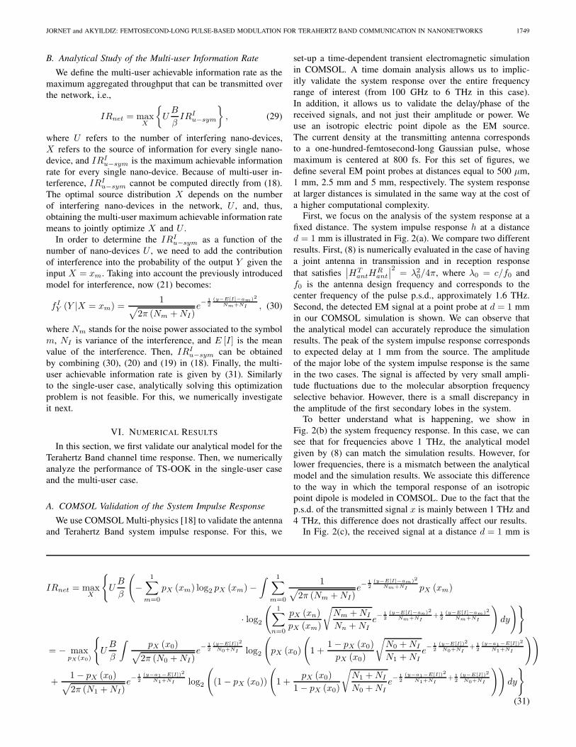
We use COMSOL Multi-physics [18] to validate the antennaand Terahertz Band system impulse response. For this, we
set-up a time-dependent transient electromagnetic simulationin COMSOL. A time domain analysis allows us to implic-itly validate the system response over the entire frequencyrange of interest (from 100 GHz to 6 THz in this case).In addition, it allows us to validate the delay/phase of thereceived signals, and not just their amplitude or power. Weuse an isotropic electric point dipole as the EM source.The current density at the transmitting antenna correspondsto a one-hundred-femtosecond-long Gaussian pulse, whosemaximum is centered at 800 fs. For this set of figures, wedefine several EM point probes at distances equal to 500 μm,1 mm, 2.5 mm and 5 mm, respectively. The system responseat larger distances is simulated in the same way at the cost ofa higher computational complexity.
First, we focus on the analysis of the system response at afixed distance. The system impulse response h at a distanced = 1 mm is illustrated in Fig. 2(a). We compare two differentresults. First, (8) is numerically evaluated in the case of havinga joint antenna in transmission and in reception responsethat satisfies
∣∣HTantH
Rant
∣∣2 = λ20/4π, where λ0 = c/f0 and
f0 is the antenna design frequency and corresponds to thecenter frequency of the pulse p.s.d., approximately 1.6 THz.Second, the detected EM signal at a point probe at d = 1 mmin our COMSOL simulation is shown. We can observe thatthe analytical model can accurately reproduce the simulationresults. The peak of the system impulse response correspondsto expected delay at 1 mm from the source. The amplitudeof the major lobe of the system impulse response is the samein the two cases. The signal is affected by very small ampli-tude fluctuations due to the molecular absorption frequencyselective behavior. However, there is a small discrepancy inthe amplitude of the first secondary lobes in the system.
To better understand what is happening, we show inFig. 2(b) the system frequency response. In this case, we cansee that for frequencies above 1 THz, the analytical modelgiven by (8) can match the simulation results. However, forlower frequencies, there is a mismatch between the analyticalmodel and the simulation results. We associate this differenceto the way in which the temporal response of an isotropicpoint dipole is modeled in COMSOL. Due to the fact that thep.s.d. of the transmitted signal x is mainly between 1 THz and4 THz, this difference does not drastically affect our results.
In Fig. 2(c), the received signal at a distance d = 1 mm is
IRnet = maxX
{UB
β
(−
1∑m=0
pX (xm) log2 pX (xm)−∫ 1∑
m=0
1√2π (Nm +NI)
e− 1
2(y−E[I]−am)2
Nm+NI pX (xm)
· log2
(1∑
n=0
pX (xn)
pX (xm)
√Nm +NI
Nn +NIe− 1
2(y−E[I]−an)2
Nm+NI+ 1
2(y−E[I]−am)2
Nm+NI
)dy
)}
= − maxpX(x0)
{UB
β
∫pX (x0)√
2π (N0 +NI)e− 1
2(y−E[I])2
N0+NI log2
(pX (x0)
(1 +
1− pX (x0)
pX (x0)
√N0 +NI
N1 +NIe− 1
2(y−E[I])2
N0+NI+ 1
2
(y−a1−E[I])2
N1+NI
))
+1− pX (x0)√2π (N1 +NI)
e− 1
2
(y−a1−E[I])2
N1+NI log2
((1− pX (x0))
(1 +
pX (x0)
1− pX (x0)
√N1 +NI
N0 +NIe− 1
2
(y−a1−E[I])2
N1+NI+ 1
2(y−E[I])2
N0+NI
))dy
}
(31)

1750 IEEE TRANSACTIONS ON COMMUNICATIONS, VOL. 62, NO. 5, MAY 2014
0 2 4 6 8 10−1
−0.5
0
0.5
1
1.5
2x 10
−3
Time [ps]
h(t)
COMSOLModel
(a) System impulse response h (t) at d = 1 mm
0.5 1 1.5 2 2.5 3 3.5 4 4.5 5 5.5 60
1
2
x 10−4
Frequency [THz]
|H(f
)|2
COMSOLModel
(b) P.s.d. of the system frequency response |H (f) |2 at d = 1 mm
0 2 4 6 8 10−3
−2
−1
0
1
2
3
4x 10
−5
Time [ps]
y(t)
[V]
COMSOLModel
(c) Received signal y (t) at d = 1 mm
1 2 3 4 5 60
0.2
0.4
0.6
0.8
1x 10
−10
Frequency [THz]
SY(f
) [W
/TH
z]
COMSOLModel
(d) P.s.d. of the received signal SY (f) at d = 1 mm
0 2 4 6 8 10 12 14 16 18 20
−5
0
5
10x 10
−5
Time [ps]
y(t)
[V]
COMSOLModel
d=1 mm
d=0.5 mm
d=2.5 mm d=5 mm
(e) Received signal y (t) at different distances d.
Fig. 2. Terahertz Band system model validation with COMSOL Multi-physics.
illustrated. The received signal analytical model can accuratelyreproduce the results obtained in the COMSOL simulations.The delay in the maximum of the received signal perfectlymatches in the two cases. The shape of the received pulsesis also very similar. Once again, the differences originatein the impulse response of the electric point dipole used inCOMSOL. This can be observed by comparing the p.s.d. ofthe received signal y, which is illustrated in Fig. 2(d). Finally,the distance dependence of the system impulse response isalso validated, by analyzing the received signal at differentdistances. In Fig. 2(e), the received signal y at distances equalto 500 μm, 1 mm, 2.5 mm and 5 mm are shown, which furthervalidates our analytical model. In the rest of the section, weuse the system model to analyze the performance of TS-OOK.
B. Single-user Achievable Information Rate in TS-OOK
After the validation of the pulse propagation properties, wenumerically investigate the maximum achievable informationrate for TS-OOK in the single-user case.
1) Received Signal Power and Noise Power Ratios: Firstof all, it is convenient to visualize the behavior of the receivedpulse power and noise power with the distance. The received
signal power P1 when a pulse has been transmitted is shownin Fig. 3(a) as a function of the transmission distance d.In the same figure, the noise powers associated with thetransmission of a pulse and the transmission of silence, N1
and N0, respectively, are also represented as functions of thetransmission distance d. In particular,
• For distances below a few millimeters, the received pulsepower P1 is much larger than the power of the molecularabsorption noise N1.
• For longer transmission distances, the received signalpower P1 and the noise power N1 generated by thetransmitted pulse decrease, but the latter does so ata lower pace. More noise is generated as the signalpropagates, but this is spread over a larger volume.
• The power N0 associated with the transmission of silenceis constant with distance and usually much smaller thanN1. This asymmetry in the noise behavior is the maindifference with respect to the classical AWGN channel.
In Fig. 3(b), the signal to noise ratio when a pulse is transmit-ted S1N1R = P1/N1 and the pulse-noise-power to silence-noise-power ratio N1/N0 are shown as functions of d. Thesetwo ratios play a major role in the achievable information rate

JORNET and AKYILDIZ: FEMTOSECOND-LONG PULSE-BASED MODULATION FOR TERAHERTZ BAND COMMUNICATION IN NANONETWORKS 1751
10−4
10−3
10−2
10−1
100
10−10
10−8
10−6
10−4
10−2
100
Distance [m]
Pow
er [n
W]
P
1
N1
N0
(a) Received signal power P1, noise power when a pulse is transmitted N1,and noise power associated with silence N0 (Ep = 0.01 aJ).
10−4
10−3
10−2
10−1
100
10−2
100
102
104
106
Distance [m]
[uni
tless
]
S
1 N
1R
N1 / N
0
Ep=1, 0.1, 0.01 aJ
(b) Signal to noise ratio when a pulse is transmitted S1N1R and pulse noisepower to silence noise power ratio N1/N0.
10−4
10−3
10−2
10−1
100
0
0.2
0.4
0.6
0.8
1
Distance [m]
IRu−
sym
[bit/
sym
bol]
Ep = 0.01 aJ
Ep = 0.1 aJ
Ep = 1 aJ
Ep = 1 aJ, AWGN
(c) Single-user information rate in bit/symbol for different noise power N1 andN0 ratios.
10−4
10−3
10−2
10−1
100
0.5
0.52
0.54
0.56
0.58
Distance [m]P
X(x
0)
Ep = 0.01 aJ
Ep = 0.1 aJ
Ep = 1 aJ
Ep = 1 aJ, AWGN
(d) Optimal probability to transmit a logical “0” for different noise powerN1 and N0 ratios.
Fig. 3. Numerical analysis of the single-user achievable information rate in TS-OOK.
and the probability source distribution for which it is achieved,as we explain next.
2) Achievable Information Rate: The single-user maximumachievable information rate IRu−sym in (22) in bit/symbol isshown in Fig. 3(c) as a function of the transmission distanced, for different values for the transmitted pulse energy Ep.Besides the Terahertz Band asymmetric noise model describedin Sec. IV-A, we also evaluate the case in which the same noisepower affects the transmission of pulses and of silences, as inthe classical AWGN channel. The results are as follows:
• For transmission distances below a few millimeters,the information rate is almost constant and equal to1 bit/symbol, which is the maximum information persymbol that can be transmitted in a binary system. Forexample, if β = 1000 and B = 10 THz, the single-userinformation rate is approximately 10 Gigabit/second. Ifβ = 10, information rates in the order of 1 Terabit/secondare possible. Ultimately, the achievable information rateis limited but the symbol generation rate and the maxi-mum rate at which the electronics at the receiver side canprocess the received signals. The use of graphene andother very high-electron-mobility materials, will enablethe processing at speeds up to a few Terabits per second,thus, making the most out of the Terahertz Band channel.
• As the transmission distance increases, the achievableinformation rate decreases, but it does so at a lower pacethan in the case of the symmetric additive Gaussian noisechannel. This phenomenon can be explained as follows.When the transmission distance increases, the receivedsignal power P1 associated with the transmission of apulse and the noise power N1 created by the propagation
of this pulse become comparable and, thus, the pulse tonoise ratio, S1N1R, tends to one. However, as long as thetotal signal power received is higher than the backgroundnoise level N0, the receiver can still distinguish betweena transmission and a no-transmission, because the p.d.f.sof the two signals are largely different.
• When the transmission distance further increases, thenoise power N1 tends to N0, and thus, the achievableinformation rate tends to zero because the symbols cannotbe distinguished, as expected.
3) Optimal Source Probability Distribution: The asym-metric behavior of the Terahertz channel is also reflectedon the optimal source probability distribution X for whichthe maximum achievable information rate is achieved. Theoptimal probability to transmit a logical “0” pX (X0) forwhich the maximum rate is achieved is shown in Fig. 3(d) asa function of the transmission distance d for different valuesof the pulse-noise-power to silence-noise-power ratio N1/N0.In particular,
• For transmission distances below a few millimeters, theoptimal source probability distribution corresponds to thebinary equiprobable distribution (pX (x0) = pX (x1) =0.5), as in the symmetric AWGN channel.
• When the transmission distance increases, even if bothsilence and pulses can be easily detected, the optimalprobability distribution is no longer the equiprobable one,but one that favors the transmission of silence rather thanpulses, because the total noise or equivocation is muchlower when zeros are transmitted. In particular, pX (x0)approaches 0.55 for distances above 10 mm.

1752 IEEE TRANSACTIONS ON COMMUNICATIONS, VOL. 62, NO. 5, MAY 2014
10−4
10−2
100
100
102
104
106
0
0.5
1
Distance [m]Number of Users [U]
IRI u−
sym
[bit/
sym
bol]
(a) Single-user achievable information rate for ev-ery single nano-device.
10−4
10−2
100
100
102
104
106
100200300400500
Distance [m]Number of Users [U]
IRne
t [bit/
sym
bol]
(b) Aggregated multi-user achievable informationrate.
10−4
10−2
100
100
102
104
106
0.40.60.8
Distance [m]Number of Users [U]
p X(x
0)
(c) Optimal probability to transmit a logical “0”.
Fig. 4. Numerical analysis of the multi-user achievable information rate in TS-OOK.
Ultimately, these results motivate the development of channelcoding schemes in which more zeros than ones are used. Atthe same time, by utilizing codes that make the transmitterto stay silent for long periods of time can compromise thesynchronization needed between transmitter and receiver. Forthe time being, synchronization schemes for ultra-broadbandpulse-based communications in the Terahertz Band do notexist, and will be developed as part of our future work.
C. Multi-user Achievable Information Rate in TS-OOK
In this section, we quantitatively study the effects of in-terference on the achievable information rate of a singleuser and on the aggregated throughput. The energy of atransmitted pulse is kept constant and equal to 0.01 aJ. Theratio between the time between pulses and the pulse durationis kept constant and equal to β = 1000. For the computationof the interference, we consider the neighboring nodes to beuniformly distributed in a 1-meter radius disk centered at thereceiver.
1) Single-user Achievable Information Rate with Multi-userInterference: In Fig. 4(a), the achievable information ratefor every nano-device IRI
u−sym in bit/symbol, obtained from(18), (19) and (20) in (30), is shown as a function of thenumber of nano-devices U and the transmission distance d.The results show that
• For a low number of interfering nano-devices, the achiev-able information rate behaves with distance similarly tothe single-user case studied in Sec. VI-B.
• As the number of interfering nano-devices increases,the total interference becomes the dominant term in theequivocation of the channel. As a result, the achievableinformation rate of every user tends to zero. Interferenceaffects in the same way the reception of noise and thereception of pulses and, thus, once it becomes the dom-inant contribution to the received signal, the achievableinformation rate degrades quickly.
2) Multi-user Achievable Information Rate and OptimalSource Probability Distribution: The multi-user achievableinformation rate IRnet in (31) as a function of the numberof interfering nano-devices U and the transmission distanced is shown in Fig. 4(b). Different trends for the multi-userachievable information rate can be observed depending onthe transmission distance and the number of nano-devices.To understand this behavior, it is important to identify which
is the optimal source probability distribution X for whichthe multi-user achievable information rate is achieved. InFig. 4(c), the optimal probability to transmit a logical “0”pX (x0), for which the single-user achievable information rateand the aggregated multi-user achievable information rate areachieved, is shown as a function of the number of nano-devicesU and the transmission distance d.
In the multi-user scenario, the optimal source distributionclearly prioritizes the transmission of logical “0”s or silenceover logical “1”s or pulses, i.e., pX (x0) � pX (x1). This isdue to the fact that by transmitting silence, both the molecularabsorption noise and especially the interference power aredrastically reduced. Indeed, this result is just numericallystating that collisions between silence are never harmful, and,thus, it is more convenient for the entire network to minimizethe number of pulses that are sent. This behavior is notseen in PAM or PPM modulations, where the informationis modulated in the shape or the position of the pulses, andpulses are always transmitted. In TS-OOK, the informationis ultimately placed in the presence or absence of “signal”(in this case a pulse due to technology limitations, but couldbe just any signal shape or even noise). This result motivatesthe development of channel coding schemes suited for nano-devices and which maximize the number of logical “0”s. Atthe same time, by transmitting less pulses, the total energyconsumption for every device is also reduced. However, thetransmission of sequences with a very large number of “0”smight hamper the synchronization among the transmittingand the receiving nano-devices. Finally, for the highest nodedensities, the Gaussian approximation might not hold anylonger, due to the fact that the probability to transmit a pulsetends to 0 and thus, the interference tends to 0. However,the utilized model is sufficient to illustrate the trends in theachievable rates.
We can now explain the behavior of the multi-user achiev-able information rate for the different transmission distances:
• When the transmission distance is short, below a fewtens of millimeters, the multi-user achievable informationrate increases with the number U of nano-devices up toa point at which it reaches a constant value. This effectappears because, even when the number of interferingnano-devices is drastically increased, provided that theindividual probability to transmit silence is much higherthan the probability to transmit a pulse (pX (x0) �
JORNET and AKYILDIZ: FEMTOSECOND-LONG PULSE-BASED MODULATION FOR TERAHERTZ BAND COMMUNICATION IN NANONETWORKS 1753
pX (x1)), the total interference does not increase at thesame pace. Thus, the received signal power is sufficientlylarge to be distinguishable from the reception of silence.
• When the transmission distance is increased, even bytransmitting primarily silence, the power of the receivedsignal when a pulse is transmitted diminishes very fastbecause of the very high path-loss of the Terahertz Band,and it is very difficult for the receiver to discern betweenpulses and silence. It is interesting to note that, fortransmission distances above a few tens of millimeters,there is an optimal number of users for which themulti-user achievable information rate is maximum. Theoptimal point is again related to the relation betweenthe transmitted and received pulse energy and the totalinterference power.
VII. CONCLUSIONS
Wireless communication among nano-devices will boost theapplications of nanotechnology in many fields of our society,ranging from healthcare to homeland security and environmen-tal protection. However, enabling the communication amongnano-devices is still an unsolved challenge. In this paper, wepresented a modulation and channel access scheme for nano-devices, which is based on the exchange of femtosecond-long pulses by following an on-off keying modulation spreadin time. We studied the performance of this new paradigmanalytically and provided numerical solutions to the maximalachievable information rate for the single-user and the multi-user cases. We developed analytical models for the path-loss,molecular absorption noise and interference in the TerahertzBand, which is the expected frequency range of operation ofnovel plasmonic nano-antennas and nano-transceivers. Thesemodels have been validated by means of extensive time-domain electromagnetic simulations with COMSOL.
The results show that the proposed modulation can supporta very large number of nano-devices simultaneously trans-mitting at multiple Gigabits-per-second and up to Terabits-per-second, depending on the modulation parameters andthe network conditions and given that asymmetric channelcoding schemes are used to prioritize the transmission ofsilence. Indeed, both the maximum single-user and multi-user information rates are achieved when asymmetric sourceprobability distributions are used, contrary to the classicalsymmetric AWGN channel. This study stimulates discussionand further research on synchronization, channel coding andmedium access for nanonetworks.
REFERENCES
[1] J. M. Jornet and I. F. Akyildiz, “Information capacity of pulse-basedwireless nanosensor networks,” in Proc. 2011 IEEE CommunicationsSociety Conference on Sensor, Mesh and Ad Hoc Communications andNetworks.
[2] I. F. Akyildiz and J. M. Jornet, “Electromagnetic wireless nanosensornetworks,” Nano Commun. Networks J., vol. 1, no. 1, pp. 3–19, Mar.2010.
[3] S. Abadal, E. Alarcon, A. Cabellos-Aparicio, M. Lemme, and M. Ne-mirovsky, “Graphene-enabled wireless communication for massive mul-ticore architectures,” IEEE Commun. Mag., vol. 51, no. 11, pp. 137–143,2013.
[4] A. K. Geim and K. S. Novoselov, “The rise of graphene,” NatureMaterials, vol. 6, no. 3, pp. 183–191, Mar. 2007.
[5] M. Tamagnone, J. S. Gomez-Diaz, J. R. Mosig, and J. Perruisseau-Carrier, “Reconfigurable terahertz plasmonic antenna concept using agraphene stack,” Applied Physics Lett., vol. 101, no. 21, p. 214102,2012.
[6] J. M. Jornet and I. F. Akyildiz, “Graphene-based plasmonic nano-antenna for terahertz band communication in nanonetworks,” IEEE J.Sel. Areas Commun., vol. 12, no. 12, pp. 685–694, Dec. 2013.
[7] H. Song and T. Nagatsuma, “Present and future of terahertz communi-cations,” IEEE Trans. Terahertz Science and Technol., 2011.
[8] T. Kurner and S. Priebe, “Towards THz communications-status inresearch, standardization and regulation,” J. Infrared, Millimeter, andTerahertz Waves, vol. 35, no. 1, pp. 53–62, 2014.
[9] I. F. Akyildiz, J. M. Jornet, and C. Han, “Terahertz band: next frontierfor wireless communications,” Physical Commun. J., vol. 12, pp. 16–32,Sep. 2014.
[10] W. Knap, F. Teppe, N. Dyakonova, D. Coquillat, and J. Lusakowski,“Plasma wave oscillations in nanometer field effect transistors forterahertz detection and emission,” J. Physics: Condensed Matter, vol. 20,no. 38, p. 384205, 2008.
[11] L. Vicarelli, M. S. Vitiello, D. Coquillat, A. Lombardo, A. C. Ferrari,W. Knap, M. Polini, V. Pellegrini, and A. Tredicucci, “Graphenefield-effect transistors as room-temperature terahertz detectors,” NatureMaterials, vol. 11, pp. 865–871, Oct. 2012.
[12] M. C. Wanke, M. Lee, C. D. Nordquist, M. J. Cich, M. Cavaliere, A. M.Rowen, J. R. Gillen, C. L. Arrington, A. D. Grine, C. T. Fuller, and J. L.Reno, “Integrated chip-scale thz technology,” Proc. SPIE, pp. 80 310E–80 310E–10, 2011.
[13] H.-J. Song, K. Ajito, Y. Muramoto, A. Wakatsuki, T. Nagatsuma, andN. Kukutsu, “24 gbit/s data transmission in 300 GHz band for futureterahertz communications,” Electron. Lett., vol. 48, no. 1, pp. 953–954,July 2012.
[14] C. Wang, C. Lin, Q. Chen, B. Lu, X. Deng, and J. Zhang, “A 10-gbit/swireless communication link using 16-QAM modulation in 140-GHzband,” IEEE Trans. Microwave Theory and Techniques, vol. 61, no. 7,pp. 2737–2746, July 2013.
[15] S. Koenig, D. Lopez-Diaz, J. Antes, F. Boes, R. Henneberger,A. Leuther, A. Tessmann, R. Schmogrow, D. Hillerkuss, R. Palmer,et al., “Wireless sub-THz communication system with high data rate,”Nature Photonics, vol. 7, no. 12, pp. 977–981, 2013.
[16] M. Win and R. Scholtz, “Ultra-wide bandwidth time-hopping spread-spectrum impulse radio for wireless multiple-access communications,”IEEE Trans. Commun., vol. 48, no. 4, pp. 679–689, 2000.
[17] W. Brown, B. Wallin, D. Lesniewski, D. Gooding, and J. Martin,“The experimental determination of on-off keying laser communicationsprobability models and a comparison with theory,” Proc., pp. 61 050U–61 050U–8, 2006.
[18] COMSOL Multiphysics Simulation Software. COMSOL. Available:http://www.comsol.com/products/multiphysics/
[19] Q. Gu, Z. Xu, H.-Y. Jian, B. Pan, X. Xu, M.-C. Chang, W. Liu, andH. Fetterman, “CMOS THz generator with frequency selective negativeresistance tank,” IEEE Trans. Terahertz Sci. and Technol., vol. 2, no. 2,pp. 193–202, 2012.
[20] E. Ojefors, B. Heinemann, and U. Pfeiffer, “Subharmonic 220-and 320-GHz SiGe HBT receiver front-ends,” IEEE Trans. Microwave Theoryand Techniques, vol. 60, no. 5, pp. 1397–1404, 2012.
[21] V. Radisic, K. Leong, X. Mei, S. Sarkozy, W. Yoshida, and W. Deal,“Power amplification at 0.65 THz using InP HEMTs,” IEEE Trans.Microwave Theory and Techniques, vol. 60, no. 3, pp. 724–729, 2012.
[22] K. Shinohara, D. Regan, Y. Tang, A. Corrion, D. Brown, J. Wong,J. Robinson, H. Fung, A. Schmitz, T. Oh, S. Kim, P. Chen, R. Nagele,A. Margomenos, and M. Micovic, “Scaling of GaN HEMTs and Schot-tky diodes for submillimeter-wave MMIC applications,” IEEE Trans.Electron. Devices, vol. 60, no. 10, pp. 2982–2996, 2013.
[23] D. Woolard, P. Zhao, C. Rutherglen, Z. Yu, P. Burke, S. Brueck, andA. Stintz, “Nanoscale imaging technology for THz-frequency transmis-sion microscopy,” International J. High Speed Electron. and Systems,vol. 18, no. 1, pp. 205–222, 2008.
[24] A. Shlivinski, E. Heyman, and R. Kastner, “Antenna characterization inthe time domain,” IEEE Trans. Antennas Propag., vol. 45, no. 7, pp.1140–1149, 1997.
[25] A. E. C. Tan, M. Y. W. Chia, K. K. M. Chan, and K. Rambabu,“Modeling the transient radiated and received pulses of ultra-widebandantennas,” IEEE Trans. Antennas Propag., vol. 61, no. 1, pp. 338–345,2013.
[26] K. Yasuko and S. Takamasa, “Terahertz-wave propagation model,” J. ofthe National Institute of Inf. and Commun. Technol., vol. 55, no. 1, pp.73–77, 2008.

1754 IEEE TRANSACTIONS ON COMMUNICATIONS, VOL. 62, NO. 5, MAY 2014
[27] T. Kleine-Ostmann, C. Jastrow, S. Priebe, M. Jacob, T. Kurner, andT. Schrader, “Measurement of channel and propagation properties at300 GHz,” in Proc. 2012 Conference on Precision ElectromagneticMeasurements, pp. 258–259.
[28] S. Priebe and T. Kurner, “Stochastic modeling of thz indoor radiochannels,” IEEE Trans. Wireless Commun., vol. 12, no. 9, pp. 4445–4455, 2013.
[29] J. M. Jornet and I. F. Akyildiz, “Channel modeling and capacity analysisof electromagnetic wireless nanonetworks in the terahertz band,” IEEETrans. Wireless Commun., vol. 10, no. 10, pp. 3211–3221, Oct. 2011.
[30] C. Jansen, S. Priebe, C. Moller, M. Jacob, H. Dierke, M. Koch, andT. Kurner, “Diffuse scattering from rough surfaces in thz communicationchannels,” IEEE Trans. Terahertz Sci. and Technol., vol. 1, no. 2, pp.462–472, 2011.
[31] J. W. Song, G. R. Aizin, J. Mikalopas, Y. Kawano, K. Ishibashi, N. Aoki,J. L. Reno, Y. Ochiai, and J. P. Bird, “Bolometric terahertz detectionin pinched-off quantum point contacts,” Applied Physics Lett., vol. 97,no. 8, p. 083109, 2010.
[32] F. Sizov and A. Rogalski, “THz detectors,” Progress in QuantumElectron., vol. 34, no. 5, pp. 278–347, 2010.
[33] V. Y. Kachorovskii, S. L. Rumyantsev, W. Knap, and M. Shur, “Perfor-mance limits for field effect transistors as terahertz detectors,” AppliedPhysics Lett., vol. 102, no. 22, 2013.
[34] R. G. Cid-Fuentes, J. M. Jornet, E. Alarcon, and I. F. Akyildiz, “Areceiver architecture for pulse-based electromagnetic nanonetworks inthe terahertz band,” in Proc. 2012 IEEE International Conference onCommunications.
[35] F. Box, “Utilization of atmospheric transmission losses for interference-resistant communications,” IEEE Trans. Commun., vol. 34, no. 10, pp.1009–1015, Oct. 1986.
[36] R. M. Goody and Y. L. Yung, Atmospheric Radiation: Theoretical Basis,2nd ed. Oxford University Press, 1989.
[37] A. Papoulis and S. U. Pillai, Probability, Random Variables and Stochas-tic Processes. McGraw-Hill, 2002.
[38] P. Cardieri, “Modeling interference in wireless ad hoc networks,” IEEECommun. Surveys and Tutorials, vol. 12, no. 4, pp. 551–572, 2010.
[39] J. Andrews, R. Ganti, M. Haenggi, N. Jindal, and S. Weber, “A primeron spatial modeling and analysis in wireless networks,” IEEE Commun.Mag., vol. 48, no. 11, pp. 156–163, Nov. 2010.
[40] M. Win, P. Pinto, and L. Shepp, “A mathematical theory of networkinterference and its applications,” Proc. IEEE, vol. 97, no. 2, pp. 205–230, Feb. 2009.
Josep Miquel Jornet received the Engineering De-gree in Telecommunication and the Master of Sci-ence in Information and Communication Technolo-gies from the Universitat Politecnica de Catalunya,Barcelona, Spain, in 2008. He received the Ph.D.degree in Electrical and Computer Engineering fromthe Georgia Institute of Technology, Atlanta, GA,in 2013, with a fellowship from “la Caixa” (2009-2010) and Fundacion Caja Madrid (2011-2012).He is currently an Assistant Professor with theDepartment of Electrical Engineering at the State
University of New York (SUNY) at Buffalo. From September 2007 toDecember 2008, he was a visiting researcher at the Massachusetts Instituteof Technology (MIT), Cambridge, under the MIT Sea Grant program. Hewas the recipient of the Oscar P. Cleaver Award for outstanding graduatestudents in the School of Electrical and Computer Engineering, at the GeorgiaInstitute of Technology in 2009. He also received the Broadband WirelessNetworking Lab Researcher of the Year Award at the Georgia Institute ofTechnology in 2010. He is a member of the IEEE and the ACM. His currentresearch interests are in electromagnetic nanonetworks, graphene-enabledwireless communication, Terahertz Band communication networks and theInternet of Nano-Things.
Ian F. Akyildiz received the B.S., M.S., and Ph.D.degrees in Computer Engineering from the Univer-sity of Erlangen-Nurnberg, Germany, in 1978, 1981and 1984, respectively. Currently, he is the KenByers Chair Professor in Telecommunications withthe School of Electrical and Computer Engineering,Georgia Institute of Technology, Atlanta, the Direc-tor of the Broadband Wireless Networking (BWN)Laboratory and the Chair of the TelecommunicationGroup at Georgia Tech. Since 2013, he is a FiDiProProfessor (Finland Distinguished Professor Program
(FiDiPro) supported by the Academy of Finland) in the Department ofElectronics and Communications Engineering, at Tampere University of Tech-nology, Finland, and the founding director of NCC (Nano CommunicationsCenter). Since 2008, he is also an honorary professor with the School of Elec-trical Engineering at Universitat Politecnica de Catalunya (UPC) in Barcelona,Catalunya, Spain and the founding director of N3Cat (NaNoNetworkingCenter in Catalunya). Since 2011, he is a Consulting Chair Professor at theDepartment of Information Technology, King Abdulaziz University (KAU)in Jeddah, Saudi Arabia. He is the Editor-in-Chief of Computer Networks(Elsevier) Journal, and the founding Editor-in-Chief of the Ad Hoc Networks(Elsevier) Journal, the Physical Communication (Elsevier) Journal and theNano Communication Networks (Elsevier) Journal. He is an IEEE Fellow(1996) and an ACM Fellow (1997). He received numerous awards from IEEEand ACM. His current research interests are in nanonetworks, Terahertz Bandcommunication networks, Long Term Evolution Advanced (LTE-A) networks,cognitive radio networks and wireless sensor networks.