
1740A Series, 1750A Series, & 1760 Series Waveform/Vector...
350
Service Manual 1740A Series, 1750A Series, & 1760 Series Waveform/Vector Monitors S/N B020000 and Above 070-8469-03 This document applies to firmware version 2.00 and above. Warning The servicing instructions are for use by qualified personnel only. To avoid personal injury, do not perform any servicing unless you are qualified to do so. Refer to all safety summaries prior to performing service. www.tektronix.com
Transcript of 1740A Series, 1750A Series, & 1760 Series Waveform/Vector...

Service Manual
1740A Series, 1750A Series, & 1760 Series
Waveform/Vector Monitors
S/N B020000 and Above
070-8469-03
This document applies to firmware version 2.00and above.
WarningThe servicing instructions are for use by qualifiedpersonnel only. To avoid personal injury, do notperform any servicing unless you are qualified todo so. Refer to all safety summaries prior toperforming service.
www.tektronix.com
Copyright © Tektronix, Inc. All rights reserved.
Tektronix products are covered by U.S. and foreign patents, issued and pending. Information in this publication supercedes
that in all previously published material. Specifications and price change privileges reserved.
Tektronix, Inc., P.O. Box 500, Beaverton, OR 97077
TEKTRONIX and TEK are registered trademarks of Tektronix, Inc.

WARRANTY
Tektronix warrants that the products that it manufactures and sells will be free from defects in materials and
workmanship for a period of three (3) years from the date of shipment. If a product proves defective during this
warranty period, Tektronix, at its option, either will repair the defective product without charge for parts and labor,
or will provide a replacement in exchange for the defective product.
In order to obtain service under this warranty, Customer must notify Tektronix of the defect before the expiration
of the warranty period and make suitable arrangements for the performance of service. Customer shall be
responsible for packaging and shipping the defective product to the service center designated by Tektronix, with
shipping charges prepaid. Tektronix shall pay for the return of the product to Customer if the shipment is to a
location within the country in which the Tektronix service center is located. Customer shall be responsible for
paying all shipping charges, duties, taxes, and any other charges for products returned to any other locations.
This warranty shall not apply to any defect, failure or damage caused by improper use or improper or inadequate
maintenance and care. Tektronix shall not be obligated to furnish service under this warranty a) to repair damage
resulting from attempts by personnel other than Tektronix representatives to install, repair or service the product;
b) to repair damage resulting from improper use or connection to incompatible equipment; c) to repair any
damage or malfunction caused by the use of non-Tektronix supplies; or d) to service a product that has been
modified or integrated with other products when the effect of such modification or integration increases the time
or difficulty of servicing the product.
THIS WARRANTY IS GIVEN BY TEKTRONIX IN LIEU OF ANY OTHER WARRANTIES, EXPRESS
OR IMPLIED. TEKTRONIX AND ITS VENDORS DISCLAIM ANY IMPLIED WARRANTIES OF
MERCHANTABILITY OR FITNESS FOR A PARTICULAR PURPOSE. TEKTRONIX’
RESPONSIBILITY TO REPAIR OR REPLACE DEFECTIVE PRODUCTS IS THE SOLE AND
EXCLUSIVE REMEDY PROVIDED TO THE CUSTOMER FOR BREACH OF THIS WARRANTY.
TEKTRONIX AND ITS VENDORS WILL NOT BE LIABLE FOR ANY INDIRECT, SPECIAL,
INCIDENTAL, OR CONSEQUENTIAL DAMAGES IRRESPECTIVE OF WHETHER TEKTRONIX OR
THE VENDOR HAS ADVANCE NOTICE OF THE POSSIBILITY OF SUCH DAMAGES.


1740A Series, 1750A Series, & 1760 Series Service Manual i
Table of Contents
General Safety Summary ix. . . . . . . . . . . . . . . . . . . . . . . . . . . . . . . . . . .
Service Safety Summary xi. . . . . . . . . . . . . . . . . . . . . . . . . . . . . . . . . . . .
Preface xiii. . . . . . . . . . . . . . . . . . . . . . . . . . . . . . . . . . . . . . . . . . . . . . . . . . .Contacting Tektronix xiv. . . . . . . . . . . . . . . . . . . . . . . . . . . . . . . . . . . . . . . . . . . . .
Specifications
Product Description 1--1. . . . . . . . . . . . . . . . . . . . . . . . . . . . . . . . . . . . . . . . . . . . . .Input Format 1--13. . . . . . . . . . . . . . . . . . . . . . . . . . . . . . . . . . . . . . . . . . . . . . . . . . . .Installation 2--1. . . . . . . . . . . . . . . . . . . . . . . . . . . . . . . . . . . . . . . . . . . . . . . . . . . . .Standard Accessories 2--1. . . . . . . . . . . . . . . . . . . . . . . . . . . . . . . . . . . . . . . . . . . . .Mechanical Installation 2--2. . . . . . . . . . . . . . . . . . . . . . . . . . . . . . . . . . . . . . . . . . .Electrical Installation 2--8. . . . . . . . . . . . . . . . . . . . . . . . . . . . . . . . . . . . . . . . . . . . .Rear Panel Connectors 2--9. . . . . . . . . . . . . . . . . . . . . . . . . . . . . . . . . . . . . . . . . . . .Remote Connector 2--10. . . . . . . . . . . . . . . . . . . . . . . . . . . . . . . . . . . . . . . . . . . . . . .Remote Connector Converter 2--12. . . . . . . . . . . . . . . . . . . . . . . . . . . . . . . . . . . . . . .RS232 Connector 2--13. . . . . . . . . . . . . . . . . . . . . . . . . . . . . . . . . . . . . . . . . . . . . . . .Installing Software 2--14. . . . . . . . . . . . . . . . . . . . . . . . . . . . . . . . . . . . . . . . . . . . . . .Loading Software 2--16. . . . . . . . . . . . . . . . . . . . . . . . . . . . . . . . . . . . . . . . . . . . . . . .Calibrating New Features 2--20. . . . . . . . . . . . . . . . . . . . . . . . . . . . . . . . . . . . . . . . . .Special Recovery for Power Loss During the Execution of UPGRADE 2--20. . . . .
Operating Information
Getting Started 2--23. . . . . . . . . . . . . . . . . . . . . . . . . . . . . . . . . . . . . . . . . . . . . . . . . .Operating Instructions 2--24. . . . . . . . . . . . . . . . . . . . . . . . . . . . . . . . . . . . . . . . . . . .General Menu Information 2--25. . . . . . . . . . . . . . . . . . . . . . . . . . . . . . . . . . . . . . . . .Functional Overview 2--27. . . . . . . . . . . . . . . . . . . . . . . . . . . . . . . . . . . . . . . . . . . . .Displaying a Signal 2--29. . . . . . . . . . . . . . . . . . . . . . . . . . . . . . . . . . . . . . . . . . . . . . .
Theory of Operation
Block Diagram Description 3--1. . . . . . . . . . . . . . . . . . . . . . . . . . . . . . . . . .Block Diagram 1: Input and Waveform Monitor 3--1. . . . . . . . . . . . . . . . . . . . . . . .Block Diagram 2: Vector -- SCH -- Component 3--3. . . . . . . . . . . . . . . . . . . . . . . . .Block Diagram 3: Microprocessor and Line Rate Controller 3--5. . . . . . . . . . . . . .
Circuit Theory 3--7. . . . . . . . . . . . . . . . . . . . . . . . . . . . . . . . . . . . . . . . . . . .Diagrams <1> and <2> Channel A and Channel B Inputs 3--7. . . . . . . . . . . . . . .Diagram <3> Vertical Input 3--8. . . . . . . . . . . . . . . . . . . . . . . . . . . . . . . . . . . . . . . .Diagram <4> Vertical Output 3--10. . . . . . . . . . . . . . . . . . . . . . . . . . . . . . . . . . . . . . .Diagram <5> Horizontal 3--11. . . . . . . . . . . . . . . . . . . . . . . . . . . . . . . . . . . . . . . . . .Diagram <6> Microprocessor 3--12. . . . . . . . . . . . . . . . . . . . . . . . . . . . . . . . . . . . . .Diagram <7> Dynamic Control 3--14. . . . . . . . . . . . . . . . . . . . . . . . . . . . . . . . . . . . .Diagram <8> Readout 3--15. . . . . . . . . . . . . . . . . . . . . . . . . . . . . . . . . . . . . . . . . . . .Diagram <9> DACS & Serial 3--16. . . . . . . . . . . . . . . . . . . . . . . . . . . . . . . . . . . . . .Diagram <10> Remote & 1760 Series / XROM Bus Connectors 3--16. . . . . . . . . . .

Table of Contents
ii 1740A Series, 1750A Series, & 1760 Series Service Manual
Diagram <11> Z-Axis & Control 3--17. . . . . . . . . . . . . . . . . . . . . . . . . . . . . . . . . . . .Diagram <12> Front Panel 3--18. . . . . . . . . . . . . . . . . . . . . . . . . . . . . . . . . . . . . . . . .Diagram <13> DACs & Digital Control 3--18. . . . . . . . . . . . . . . . . . . . . . . . . . . . . .Diagram <14> Subcarrier Regenerator 3--19. . . . . . . . . . . . . . . . . . . . . . . . . . . . . . .Diagram <15> Phase Shifter 3--21. . . . . . . . . . . . . . . . . . . . . . . . . . . . . . . . . . . . . . .Diagram <16> Demodulator 3--22. . . . . . . . . . . . . . . . . . . . . . . . . . . . . . . . . . . . . . .Diagram <17> Internal SCH 3--23. . . . . . . . . . . . . . . . . . . . . . . . . . . . . . . . . . . . . . .Diagram <18> Reference SCH 3--26. . . . . . . . . . . . . . . . . . . . . . . . . . . . . . . . . . . . .Diagram <19> Component Inputs, Transcoders, & RGB Outputs 3--28. . . . . . . . . .Diagram <20> Component Control and Switching (1760 Series Only) 3--30. . . . . .Diagram <21> Low Voltage Power Supply 3--32. . . . . . . . . . . . . . . . . . . . . . . . . . . .Diagram <22> High Volts Power Supply 3--35. . . . . . . . . . . . . . . . . . . . . . . . . . . . . .
Performance Verification
Recommended Equipment List 4--1. . . . . . . . . . . . . . . . . . . . . . . . . . . . . . . . . . . . .Performance Check Procedure Short-Form Reference 4--6. . . . . . . . . . . . . . . . . . .Performance Check Procedure 4--19. . . . . . . . . . . . . . . . . . . . . . . . . . . . . . . . . . . . . .
Adjustments
Required Equipment 5--1. . . . . . . . . . . . . . . . . . . . . . . . . . . . . . . . . . . . . . . . . . . . . .Initial Setup 5--9. . . . . . . . . . . . . . . . . . . . . . . . . . . . . . . . . . . . . . . . . . . . . . . . . . . .Functional Description of PC Display 5--10. . . . . . . . . . . . . . . . . . . . . . . . . . . . . . . .Circuit Board Adjustment Locations 5--12. . . . . . . . . . . . . . . . . . . . . . . . . . . . . . . . .Waveform Illustrations 5--15. . . . . . . . . . . . . . . . . . . . . . . . . . . . . . . . . . . . . . . . . . . .
Maintenance
Preventing ESD 6--1. . . . . . . . . . . . . . . . . . . . . . . . . . . . . . . . . . . . . . . . . . . . . . . . .Preventive Maintenance 6--1. . . . . . . . . . . . . . . . . . . . . . . . . . . . . . . . . . . . . . . . . . .Performance Checks and Adjustments 6--2. . . . . . . . . . . . . . . . . . . . . . . . . . . . . . . .Inspection and Cleaning 6--2. . . . . . . . . . . . . . . . . . . . . . . . . . . . . . . . . . . . . . . . . . .Replacing the Line Fuse 6--5. . . . . . . . . . . . . . . . . . . . . . . . . . . . . . . . . . . . . . . . . . .Troubleshooting 6--5. . . . . . . . . . . . . . . . . . . . . . . . . . . . . . . . . . . . . . . . . . . . . . . . .
Corrective Maintenance 6--12. . . . . . . . . . . . . . . . . . . . . . . . . . . . . . . . . . . .Circuit Boards 6--12. . . . . . . . . . . . . . . . . . . . . . . . . . . . . . . . . . . . . . . . . . . . . . . . . . .Mechanical Disassembly/Assembly 6--13. . . . . . . . . . . . . . . . . . . . . . . . . . . . . . . . . .
Removing the Bezel 6--13. . . . . . . . . . . . . . . . . . . . . . . . . . . . . . . . . . . . . . . . . .Replacing the Graticule Light 6--14. . . . . . . . . . . . . . . . . . . . . . . . . . . . . . . . . . .Removing the CRT 6--16. . . . . . . . . . . . . . . . . . . . . . . . . . . . . . . . . . . . . . . . . . .Removing the Rear Panel 6--19. . . . . . . . . . . . . . . . . . . . . . . . . . . . . . . . . . . . . .Removing the Front Panel and the Front Panel Circuit Board 6--21. . . . . . . . . .Removing the Main Board 6--22. . . . . . . . . . . . . . . . . . . . . . . . . . . . . . . . . . . . .Removing the Power Supply Board 6--24. . . . . . . . . . . . . . . . . . . . . . . . . . . . . .Removing the Vector Board 6--25. . . . . . . . . . . . . . . . . . . . . . . . . . . . . . . . . . . .Removing the SCH Board
(1750A Series & 1760 Series Option SC only) 6--26. . . . . . . . . . . . . .Removing the Component Board
(1760 Series only) 6--26. . . . . . . . . . . . . . . . . . . . . . . . . . . . . . . . . . . . .Repackaging 6--27. . . . . . . . . . . . . . . . . . . . . . . . . . . . . . . . . . . . . . . . . . . . . . . . . . . .

Table of Contents
1740A Series, 1750A Series, & 1760 Series Service Manual iii
Options and Accessories
Options 7--1. . . . . . . . . . . . . . . . . . . . . . . . . . . . . . . . . . . . . . . . . . . . . . . . . . . . . . . .Standard Accessories 7--1. . . . . . . . . . . . . . . . . . . . . . . . . . . . . . . . . . . . . . . . . . . . .Optional Accessories 7--2. . . . . . . . . . . . . . . . . . . . . . . . . . . . . . . . . . . . . . . . . . . . .
Replaceable Electrical Parts
Parts Ordering Information 8--1. . . . . . . . . . . . . . . . . . . . . . . . . . . . . . . . . . . . . . . . .Using the Replaceable Electrical Parts List 8--1. . . . . . . . . . . . . . . . . . . . . . . . . . . .
Diagrams/Circuit Board Illustrations
Replaceable Mechanical Parts
Parts Ordering Information 10--1. . . . . . . . . . . . . . . . . . . . . . . . . . . . . . . . . . . . . . . . .Using the Replaceable Mechanical Parts List 10--1. . . . . . . . . . . . . . . . . . . . . . . . . .
Glossary
Index

Table of Contents
iv 1740A Series, 1750A Series, & 1760 Series Service Manual
List of Figures
Figure 2--1: Dimensions of the 1700F00 plain cabinet 2--2. . . . . . . . . . . .
Figure 2--2: 1700F02 portable cabinet 2--3. . . . . . . . . . . . . . . . . . . . . . . . .
Figure 2--3: Rear view showing the securing screws 2--4. . . . . . . . . . . . .
Figure 2--4: The WFM7F05 side-by-side rack adapter 2--5. . . . . . . . . . .
Figure 2--5: A WFM7F05 with a blank front panel (1700F06) 2--5. . . . .
Figure 2--6: WFM7F05 rack mount cabinet with a 1700F07 utility
drawer 2--6. . . . . . . . . . . . . . . . . . . . . . . . . . . . . . . . . . . . . . . . . . . . . . .
Figure 2--7: Custom installation of an instrument 2--7. . . . . . . . . . . . . . .
Figure 2--8: Rear panel connectors 2--9. . . . . . . . . . . . . . . . . . . . . . . . . . . .
Figure 2--9: Rear panel REMOTE connector. 2--10. . . . . . . . . . . . . . . . . . .
Figure 2--10: Replacement adapter for 1740/1750 2--12. . . . . . . . . . . . . . .
Figure 2--11: Rear panel RS232 connector 2--13. . . . . . . . . . . . . . . . . . . . .
Figure 2--12: Standard and alternate hookups for the 9-pin
connector 2--16. . . . . . . . . . . . . . . . . . . . . . . . . . . . . . . . . . . . . . . . . . . . .
Figure 2--13: Standard and alternate hookups for 25-Pin PC
Connector 2--17. . . . . . . . . . . . . . . . . . . . . . . . . . . . . . . . . . . . . . . . . . . . .
Figure 2--14: 1760 front panel 2--24. . . . . . . . . . . . . . . . . . . . . . . . . . . . . . . .
Figure 2--15: The CRT menu, with the bezel controls and buttons 2--25.
Figure 3--1: NTSC line count (U24) & color frame 1 SCH field pulse 3--26
Figure 3--2: PAL line count (U24) & color frame 1 SCH field pulse 3--27
Figure 3--3: Pinout of the CRT socket 3--35. . . . . . . . . . . . . . . . . . . . . . . . .
Figure 4--1: External Horizontal or RGB/YRGB Cable Adapter 4--4. . .
Figure 4--2: Remote Sync Cable Adapter 4--5. . . . . . . . . . . . . . . . . . . . . .
Figure 4--3: Audio and Timecode Cable Adapter 4--5. . . . . . . . . . . . . . . .
Figure 4--4: Timing Cursor Check 4--16. . . . . . . . . . . . . . . . . . . . . . . . . . . .
Figure 4--5: Fast DC Restorer Response 4--24. . . . . . . . . . . . . . . . . . . . . . .
Figure 4--6: R--Y Display 4--27. . . . . . . . . . . . . . . . . . . . . . . . . . . . . . . . . . . .
Figure 4--7: Audio Display 4--33. . . . . . . . . . . . . . . . . . . . . . . . . . . . . . . . . .
Figure 4--8: Option Blanking Pulse 4--36. . . . . . . . . . . . . . . . . . . . . . . . . . .
Figure 4--9: Bowtie Common Mode Rejection Ratio 4--38. . . . . . . . . . . . .
Figure 5--1: External horizontal/RGB and YRGB cable adapter 5--5. . .
Figure 5--2: Remote sync cable adapter 5--5. . . . . . . . . . . . . . . . . . . . . . . .
Figure 5--3: Audio and Timecode Cable Adapter 5--6. . . . . . . . . . . . . . . .

Table of Contents
1740A Series, 1750A Series, & 1760 Series Service Manual v
Figure 5--4: RS232 cable standard and alternate connections for
9-pin PC connector 5--7. . . . . . . . . . . . . . . . . . . . . . . . . . . . . . . . . . . . .
Figure 5--5: RS232 cable standard and alternate hookups for
25-pin PC connector 5--8. . . . . . . . . . . . . . . . . . . . . . . . . . . . . . . . . . . .
Figure 5--6: Typical adjustment procedures PC screen display 5--10. . . .
Figure 5--7: A1 Power Supply board 5--12. . . . . . . . . . . . . . . . . . . . . . . . . .
Figure 5--8: A3 Main board 5--12. . . . . . . . . . . . . . . . . . . . . . . . . . . . . . . . . .
Figure 5--9: A5 Vector board 5--13. . . . . . . . . . . . . . . . . . . . . . . . . . . . . . . . .
Figure 5--10: A6 SCH board 5--13. . . . . . . . . . . . . . . . . . . . . . . . . . . . . . . . .
Figure 5--11: A7 Component board 5--14. . . . . . . . . . . . . . . . . . . . . . . . . . .
Figure 5--12: Adjusting for thinnest luminance step 5--15. . . . . . . . . . . . .
Figure 5--13: Matching flat and luminance filter responses 5--15. . . . . . .
Figure 5--14: Adjusting the NTSC SCH on the oscilloscope 5--16. . . . . . .
Figure 5--15: Matching the SCH dot flipping points 5--16. . . . . . . . . . . . .
Figure 5--16: Adjusting the option blanking pulse 5--17. . . . . . . . . . . . . . .
Figure 5--17: Adjusting for minimum Bowtie amplitude 5--17. . . . . . . . . .
Figure 5--18: Adjusting Diamond display phase 5--18. . . . . . . . . . . . . . . . .
Figure 6--1: Instrument etched circuit board assemblies 6--12. . . . . . . . . .
Figure 6--2: Removing the CRT bezel 6--13. . . . . . . . . . . . . . . . . . . . . . . . .
Figure 6--3: Replacing graticule light bulbs 6--15. . . . . . . . . . . . . . . . . . . .
Figure 6--4: Removing the CRT 6--17. . . . . . . . . . . . . . . . . . . . . . . . . . . . . .
Figure 6--5: Removing the rear panel and Input/BNC assembly 6--20. . .
Figure 6--6: Disassembling Input/BNC assembly A4/A4--A1 6--20. . . . . . .
Figure 6--7: Removing the front--panel assembly 6--21. . . . . . . . . . . . . . . .
Figure 6--8: Front Panel circuit board assembly 6--22. . . . . . . . . . . . . . . . .
Figure 6--9: Screws holding the Main circuit board in place 6--23. . . . . . .
Figure 6--10: Securing screws for the Power Supply circuit 6--24. . . . . . .
Figure 6--11: Mounting hardware for the Vector and SCH circuit
boards 6--25. . . . . . . . . . . . . . . . . . . . . . . . . . . . . . . . . . . . . . . . . . . . . . . .
Figure 6--12: Component circuit board mounting hardware 6--26. . . . . .
Figure 6--13: Repackaging a 1740A, 1750A, or 1760 Series
instrument 6--27. . . . . . . . . . . . . . . . . . . . . . . . . . . . . . . . . . . . . . . . . . . .
Figure 10--1: Exploded View 10--11. . . . . . . . . . . . . . . . . . . . . . . . . . . . . . . . .

Table of Contents
vi 1740A Series, 1750A Series, & 1760 Series Service Manual
List of Tables
Table 1--1: Waveform vertical deflection 1--3. . . . . . . . . . . . . . . . . . . . . .
Table 1--2: External reference 1--6. . . . . . . . . . . . . . . . . . . . . . . . . . . . . .
Table 1--3: Waveform horizontal deflection 1--6. . . . . . . . . . . . . . . . . . .
Table 1--4: Measurement cursors 1--7. . . . . . . . . . . . . . . . . . . . . . . . . . . .
Table 1--5: RGB/YRGB 1--7. . . . . . . . . . . . . . . . . . . . . . . . . . . . . . . . . . . .
Table 1--6: Calibrator 1--8. . . . . . . . . . . . . . . . . . . . . . . . . . . . . . . . . . . . .
Table 1--7: Vector mode 1--8. . . . . . . . . . . . . . . . . . . . . . . . . . . . . . . . . . . .
Table 1--8: Audio mode 1--9. . . . . . . . . . . . . . . . . . . . . . . . . . . . . . . . . . . . .
Table 1--9: Time code 1--10. . . . . . . . . . . . . . . . . . . . . . . . . . . . . . . . . . . . . .
Table 1--10: SCH Phase mode (1750 Series and
1760 Option SC Only) 1--10. . . . . . . . . . . . . . . . . . . . . . . . . . . . . . . . . .
Table 1--11: Component vector mode (1760 Series Only) 1--12. . . . . . . . .
Table 1--12: Lightning mode (1760 Series only) 1--12. . . . . . . . . . . . . . . . .
Table 1--13: Bowtie mode (1760 Series only) 1--13. . . . . . . . . . . . . . . . . . .
Table 1--14: Transcoded GBR outputs 1--13. . . . . . . . . . . . . . . . . . . . . . . .
Table 1--15: CRT display 1--14. . . . . . . . . . . . . . . . . . . . . . . . . . . . . . . . . . .
Table 1--16: Power source 1--14. . . . . . . . . . . . . . . . . . . . . . . . . . . . . . . . . . .
Table 1--17: Environmental characteristics 1--14. . . . . . . . . . . . . . . . . . . .
Table 1--18: Physical characteristics 1--15. . . . . . . . . . . . . . . . . . . . . . . . . .
Table 1--19: Certifications and compliances 1--16. . . . . . . . . . . . . . . . . . . .
Table 2--1: Remote connector 2--11. . . . . . . . . . . . . . . . . . . . . . . . . . . . . . . .
Table 2--2: The available display modes 2--27. . . . . . . . . . . . . . . . . . . . . . .
Table 3--1: Transcoder signal mixing 3--28. . . . . . . . . . . . . . . . . . . . . . . . .
Table 3--2: Component display output switching 3--29. . . . . . . . . . . . . . .
Table 4--1: Short-Form Performance Check 4--6. . . . . . . . . . . . . . . . . . . .
Table 4--2: Vector cursor readout values 4--17. . . . . . . . . . . . . . . . . . . . . .
Table 4--3: Audio and Timecode Values 4--32. . . . . . . . . . . . . . . . . . . . . . .
Table 6--1: External inspection check list 6--3. . . . . . . . . . . . . . . . . . . . . .
Table 6--2: Power supply fault symptoms 6--6. . . . . . . . . . . . . . . . . . . . . .
Table 6--3: Low volts supply voltages 6--6. . . . . . . . . . . . . . . . . . . . . . . . .
Table 6--4: Control Circuit Test Points 6--8. . . . . . . . . . . . . . . . . . . . . . . .
Table 6--5: Shut down logic levels 6--9. . . . . . . . . . . . . . . . . . . . . . . . . . . .

Table of Contents
1740A Series, 1750A Series, & 1760 Series Service Manual vii
Table 6--6: High Volts Supply Fault Symptoms 6--10. . . . . . . . . . . . . . . . .
Table 6--7: High voltage oscillator test points 6--11. . . . . . . . . . . . . . . . . .
Table 6--8: Main Board Plug Connections 6--22. . . . . . . . . . . . . . . . . . . . .
Table 7--1: Power cord identification 7--2. . . . . . . . . . . . . . . . . . . . . . . . .

Table of Contents
viii 1740A Series, 1750A Series, & 1760 Series Service Manual

1740A Series, 1750A Series, & 1760 Series Service Manual ix
General Safety Summary
Review the following safety precautions to avoid injury and prevent damage tothis product or any products connected to it. To avoid potential hazards, use thisproduct only as specified.
Only qualified personnel should perform service procedures.
Use Proper Power Cord. Use only the power cord specified for this product andcertified for the country of use.
Ground the Product. This product is grounded through the grounding conductorof the power cord. To avoid electric shock, the grounding conductor must beconnected to earth ground. Before making connections to the input or outputterminals of the product, ensure that the product is properly grounded.
Observe All Terminal Ratings. To avoid fire or shock hazard, observe all ratingsand markings on the product. Consult the product manual for further ratingsinformation before making connections to the product.
Do not apply a potential to any terminal, including the common terminal, thatexceeds the maximum rating of that terminal.
Do Not Operate Without Covers. Do not operate this product with covers or panelsremoved.
Use Proper Fuse. Use only the fuse type and rating specified for this product.
Avoid Exposed Circuitry. Do not touch exposed connections and componentswhen power is present.
Do Not Operate With Suspected Failures. If you suspect there is damage to thisproduct, have it inspected by qualified service personnel.
Do Not Operate in Wet/Damp Conditions.
Do Not Operate in an Explosive Atmosphere.
Keep Product Surfaces Clean and Dry.
Provide Proper Ventilation. Refer to the manual’s installation instructions fordetails on installing the product so it has proper ventilation.
Terms in this Manual. These terms may appear in this manual:
WARNING.Warning statements identify conditions or practices that could result
in injury or loss of life.
To Avoid Fire orPersonal Injury
Symbols and Terms

General Safety Summary
x 1740A Series, 1750A Series, & 1760 Series Service Manual
CAUTION. Caution statements identify conditions or practices that could result in
damage to this product or other property.
Terms on the Product. These terms may appear on the product:
DANGER indicates an injury hazard immediately accessible as you read themarking.
WARNING indicates an injury hazard not immediately accessible as you read themarking.
CAUTION indicates a hazard to property including the product.
Symbols on the Product. The following symbols may appear on the product:
CAUTIONRefer to Manual
WARNINGHigh Voltage
Protective Ground(Earth) Terminal

1740A Series, 1750A Series, & 1760 Series Service Manual xi
Service Safety Summary
Only qualified personnel should perform service procedures. Read this ServiceSafety Summary and the General Safety Summary before performing any serviceprocedures.
Do Not Service Alone. Do not perform internal service or adjustments of thisproduct unless another person capable of rendering first aid and resuscitation ispresent.
Disconnect Power. To avoid electric shock, switch off the instrument power, thendisconnect the power cord from the mains power.
Use Caution When Servicing the CRT. To avoid electric shock or injury, useextreme caution when handling the CRT. Only qualified personnel familiar withCRT servicing procedures and precautions should remove or install the CRT.
CRTs retain hazardous voltages for long periods of time after power is turned off.Before attempting any servicing, discharge the CRT by shorting the anode tochassis ground. When discharging the CRT, connect the discharge path to groundand then the anode. Rough handling may cause the CRT to implode. Do not nickor scratch the glass or subject it to undue pressure when removing or installing it.When handling the CRT, wear safety goggles and heavy gloves for protection.
Use Care When Servicing With Power On. Dangerous voltages or currents mayexist in this product. Disconnect power, remove battery (if applicable), anddisconnect test leads before removing protective panels, soldering, or replacingcomponents.
To avoid electric shock, do not touch exposed connections.
X-Radiation. To avoid x-radiation exposure, do not modify or otherwise alter thehigh-voltage circuitry or the CRT enclosure. X-ray emissions generated withinthis product have been sufficiently shielded.

Service Safety Summary
xii 1740A Series, 1750A Series, & 1760 Series Service Manual

1740A Series, 1750A Series, & 1760 Series Service Manual xiii
Preface
This manual provides servicing information for the 1740A/1750A/1760--Seriesof instruments. The 1750A is identical to the 1740A, except that the 1750A--Se-ries makes SCH Phase measurements. The 1760-Series adds component analogmeasurement capability to the basic 1740A-Series, and the 1760-Series OptionSC adds the same component analog measurement capability to a 1750A-Seriesinstrument.
Servicing Information
This manual supports both module level (for module exchange) and componentlevel servicing. Module level servicing uses the block diagram and its descrip-tions to isolate a problem to the circuits on a particular circuit board. Componentlevel servicing also uses the theory of operation, schematic diagrams and circuitboard parts locating illustration and cross reference indexes (part location charts).
Specific procedures for troubleshooting and disassembly in this manual shouldonly be attempted by competent service technicians. Be sure to read and followall Warnings and Cautions when performing maintenance.
The last sections of this manual contain the Replaceable Parts Lists, CircuitBoard Illustrations, and Schematic Diagrams needed to isolate and replace faultycomponents. Replacement part ordering information can be found in theMaintenance section of this manual.
Performance Verification
These instruments are designed to be returned to operation within statedspecifications through a PC-based adjustment procedure. The disk holder for thismanual contains two computer disks: 1. A software disk containing instrumentsoperating software (Version 2.2 or greater). 2. A calibration software disk.
An IBM compatible personal computer (PC) with a DOS 3.3 or higher operatingsystem, and a 31/2 inch high density floppy drive is required to perform thereadjustment procedure or reload the operating software.
The spare software disk is provided in case the Main circuit board, whichcontains the software, requires replacement. In all cases, the operating softwaremust be Version 2.2 or above to perform the Readjustment Procedure.
The specifications contained in the Specification section of this manual containPerformance Verification step numbers.

Preface
xiv 1740A Series, 1750A Series, & 1760 Series Service Manual
Contacting Tektronix
Phone 1-800-833-9200*
Address Tektronix, Inc.Department or name (if known)14200 SW Karl Braun DriveP.O. Box 500Beaverton, OR 97077USA
Web site www.tektronix.com
Sales support 1-800-833-9200, select option 1*
Service support 1-800-833-9200, select option 2*
Technical support Email: [email protected]
1-800-833-9200, select option 3*
6:00 a.m. -- 5:00 p.m. Pacific time
* This phone number is toll free in North America. After office hours, please leave avoice mail message.Outside North America, contact a Tektronix sales office or distributor; see theTektronix web site for a list of offices.

1740A Series, 1750A Series, & 1760 Series Service Manual 1- 1
Specifications
The tables in this chapter list the specifications for the 1740A, 1750A, and 1760Series waveform monitors. Items listed in the Performance Requirement columnare generally quantitative, and can be tested by the Performance Verificationprocedure in the service manual. Items listed in the Reference Informationcolumn are useful operating parameters that have typical values; information inthis column is not guaranteed.
The second column of the two column format contains all of the descriptivematerial about the listed characteristic. The performance verification procedurestep number, used to verify the characteristic, is also in this column. This seriesof instruments is designed to operate on both PAL and NTSC standards, so someof the tolerances are defined in millivolts and IREs; in these dual value toler-ances, PAL values appear in parentheses.
Performance Requirements (Req) . Items with this designation are critical toinstrument performance. In most cases, a tolerance and a performance verifica-tion step number are listed. However, there are a few areas where instrumentoperation verifies that the performance requirement is met.
Reference Information (RI). This information about the instrument operation mayhave a tolerance listed, but these should be considered as typical, not absolute.
Performance Verification Step. This item identifies the location of the test methodin the Performance Verification procedure.
The specifications listed in the Electrical Specifications portion of these tablesapply over an ambient temperature range of +0 C to +40 C. The ratedaccuracies are valid when the instrument is calibrated in an ambient temperaturerange of +20 C to +30 C.
Product Description
The 1740A/1750A/1760 Series is a half-rack width by three-rack-unit highinstrument. It is a versatile waveform monitor/vectorscope for composite andcomponent television signals. Most circuitry and the mechanical components areshared throughout the series. In addition to NTSC and PAL standard versions, adual standard (NTSC/PAL) version is available.

Specifications
1- 2 1740A Series, 1750A Series, & 1760 Series Service Manual
These instruments employ a bright, post accelerated CRT with lighted internalgraticule. The parallax free internal graticule structure contains targets andmarkings for both the vector and waveform functions. The “Lightning” graticule,for the 1760 Series, is electronic, in order to keep from complicating thewaveform/vector graticule. Option 74, which uses a white phosphor (P4) CRT, isavailable for all three instrument series.
These monitors are microprocessor controlled to provide greater versatility.Switch settings, affecting the operation of the instrument, are continuouslypolled by the processor, with any change in status acted upon immediately.Current operating conditions are preserved in Non-Volatile Random AccessMemory (NOVRAM), which returns the front panel settings to the currentsettings, in the event of power interruption (either accidental or routine powerdown).
Many operational measurements are performed on a repetitive basis, and theseinstruments provide a method of repeating common measurements by simplyselecting stored measurement settings from a CRT menu list. The commonmeasurement front panel settings can be stored and named by the user. Measure-ment specific, front-panel settings can be recalled by pushing the front-panelPreset Menu button and selecting the desired preset by name or number.
Many functions that were formerly selected by changing internal jumpers and/orwire straps are now accessible through on screen menu selections. Menus areselected by pushing the appropriate front panel Menu selection. Menu items arethen selected by pushing one or more of the assignable switches and/or rotatingthe assigned front-panel control. Once selected these menu choices are retaineduntil changed by subsequent reconfiguration.
The front panel provides both assignable switches (located next to the CRT) andcontrols (located beneath the CRT), that operate with CRT readout to increasefunctionality without cluttering the limited front panel area. Function of theseswitches and controls is dictated by the front-panel Display and initial Menuchoices.
The 1740A Series is a full capability waveform/vector monitor that also providesaudio and time code measurements. The 1750A Series has all of the capabilitiesof the 1740A Series, with the addition of SCH phase measurements.
The 1760 Series combines component measurements with the compositecapabilities of the 1740A/1750A Series. It incorporates all of the measurementsof the 1740A Series with a full set of component analog measurements. Theassignable cursors, along with the CRT readout can be used for time, voltage,and phase measurements. The system of Menus and CRT readout simplifies theconfiguration of this monitor for measurement or monitoring of signal character-istics.

Specifications
1740A Series, 1750A Series, & 1760 Series Service Manual 1- 3
Table 1- 1: Waveform vertical deflection
Characteristic Performance requirement
Deflection Factor Req: 1 V full scale (X1): 1 volt input displayed within 1% of 140 IRE (1.00 VPAL)
X5 Gain: 0.2 volt input displayed within1% of 140 IRE (1.00 VPAL)
X10 Gain: 0.1 volt input displayed within 1% of 140 IRE (1.00 VPAL)
RI: Any one of the 8 inputs
Performance Verification Procedure Step: 9
RI: 1 V, 0.2 V, and 0.1 V from accurate source (VAC) can be made full scale.
Variable Gain Range Req: 0.2X to 1.4X
Performance Verification Procedure Step: 9
RI: VAC of 1 V and 0.2 V can be displayed as full scale with appropriate Gainsettings.
Overscan Req: ≤1% variation in baseline of chroma when positioned anywhere between sync tipand 100% white
RI: X1, X5, or X10 with any variable gain setting
Performance Verification Procedure Step: 16
RI: 1 V peak to peak Modulated Sin2 composite video signal.
Frequency and Transient response performance requirements (PR), with any gainsetting, override any overscan specification.
Video Maximum Operating Input Voltage RI: --1.8 V to +2.2 V, (all inputs, A -- B3) DC+peak AC
Absolute Video Input Voltage RI: --8.5 V to +8.5 V ( DC+peak AC)
Video Input DC Impedance RI: ≥20k Ω
Video Input Return Loss RI: Typically ≥40 dB to 6 MHz
RI: Loop through terminated in 75 Ω. Power on or off.
Video Input DC Offset Between Channels Req: ≤1 IRE (7 mV PAL)
RI: Typically ≤1 mV
Performance Verification Procedure Step: 4
RI: Inputs terminated in 75 Ω.
Video Input Offset Range RI: CHA2, A3, B2, & B3 can be offset from CHA1 or CHB1 by ±350 mV
RI: No signal applied, terminated in 75 Ω and rotate Variable Gain betweenminimum and maximum.
Video Input Loop-Through Isolation RI: Typically ≥70 dB
Video Input Crosstalk Between Channels RI: Typically ≥60 dB
RI: All inputs terminated in 75 Ω.
Frequency Response (Flat) Req: ±2% to 10 MHz (X1 Gain)±4% to 10 MHz (X5 and X10 Gain), on screen signal (0.2 V or 0.1 V)
RI: Leveled Sinewave Generator
RI: All inputs AC or DC coupling
Performance Verification Procedure Step: 12

Specifications
1- 4 1740A Series, 1750A Series, & 1760 Series Service Manual
Table 1- 1: Waveform vertical deflection (Cont.)
Characteristic Performance requirement
Luminance Filter Gain Req: 1 ±1%
RI: Reference is FLAT at 50 kHz
Performance Verification Procedure Step: 13
RI: Leveled Sinewave Generator.
Luminance and chrominance filter offset is typically 1mV.
Luminance Filter Response Req: ≤3 dB attenuation at 1 MHz≥40 dB attenuation at FSCPerformance Verification Procedure Step: 13
RI: Leveled Sinewave Generator.
Luminance Filter Chrominance Rejection(1745A--1755A--1765 only)
Req: ≥34 dB
RI: Leveled Sinewave Generator.
Chrominance Filter Gain Req: 1 ±1%
RI: Ref. is flat at FSC (3.58 or 4.43 MHz)
Performance Verification Procedure Step: 14
RI: Leveled Sinewave Generator.
Luminance and chrominance filter offset is typically 1mV.
Chrominance Filter Bandwidth Req: 1.5 MHz±0.3 MHz
RI: Centered at FSC. Passband is typically FSC + and -- 750 kHz
RI: Leveled Sinewave Generator
Chrominance Filter Attenuation at 2X FSC RI: ≥25 dB
Differentiated Step Filter Attenuation at 2X FSC RI: ≥40 dB
Transient Response Req: Pulse-to-Bar Ratio 0.99:1 to 1.01:1
RI: Preshoot≤1%
RI: Overshoot≤1%
RI: Ringing ≤1%
RI: 2T pulse and bar, any gain setting.
Req: Field-Rate Tilt≤1%
RI: Field rate square wave or vertical window signal.
Req: Line-Rate Tilt ≤1%
RI: 25 s bar.
RI: Differential Gain ≤1%
Performance Verification Procedure Step: 17
Pix Out Gain Req: 1±3%
RI: Leveled Sinewave Generator and Peak-to-Peak Detector.
Pix Out Frequency Response Req: ±3% to 6 MHz
RI: A leveled sinewave generator with the output terminated in 75 Ω.
Pix Out Differential Gain RI: ≤1%

Specifications
1740A Series, 1750A Series, & 1760 Series Service Manual 1- 5
Table 1- 1: Waveform vertical deflection (Cont.)
Characteristic Performance requirement
Pix Out Differential Phase RI: ≤1°
Pix Out Output Impedance RI: 75 Ω
Pix Out Return Loss Req: Typically ≥ 30 dB to 6 MHz
RI: Power on.
Pix Out Line Select Strobe RI: (AUD) A DC offset is added to output in line select to bright up the selectedline or lines.
RI: Checked in both 15--line and 1 line.
DC Restorer 60 Hz (50 Hz) Attenuation Req: Slow Mode≤10%Fast Mode≥95%
RI: Back porch or sync tip clamp point is selected through menu.
Performance Verification Procedure Step: 18
RI: 60 Hz (50 Hz) sinewave generator.
DC Restorer Offset Error Req: ≤1 IRE (7 mV PAL)
RI: Typically 3 mV
Performance Verification Procedure Step: 4
RI: No signal applied, terminated in 75 Ω. Rotate Variable Gain between mini-mum and maximum.
Fast Settling Time RI: (AUD)≤6 video lines
Blanking Shift with 10 to 90% APL Change Req: ≤1 IRE (7 mV PAL)
Performance Verification Procedure Step: 19
RI: APL Bounce signal.
Blanking Shift with Presence and Absence ofBurst
Req: ≤1 IRE (7 mV PAL)
Performance Verification Procedure Step: 19
RI: Typically 3 mV
RI: Burst on test signal turned off and on.

Specifications
1- 6 1740A Series, 1750A Series, & 1760 Series Service Manual
Table 1- 2: External reference
Characteristic Description
Input RI: Composite video or black burst
Maximum Operating Input Voltage RI: --1.8 V to +2.2 V, DC + peak AC
Absolute Maximum Input Voltage RI: --8.5 V to +8.5 V, DC + peak AC
DC Input Impedance RI: ≥20 k Ω
Return Loss RI: Typically ≥40 dB to 6 MHz
Performance Verification Procedure Step: NO TAG
RI: Loop-through terminated in 75 Ω. Power on or off.
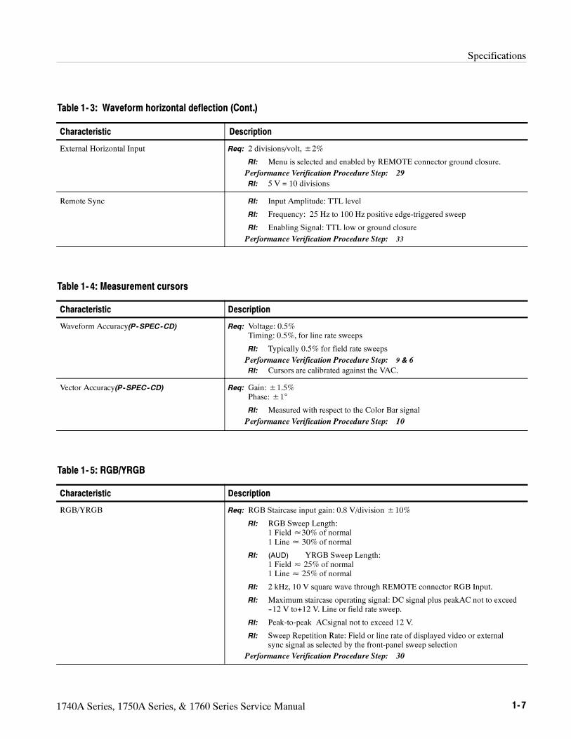
Table 1- 3: Waveform horizontal deflection
Characteristic Description
Sweep Req: Synchronization: Sweep triggered by horizontal and vertical sync pulses
RI: Sweep Length:≈12 divisions
RI: Sweep freeruns without input
Performance Verification Procedure Step: 8
Sweep Timing Accuracy Req: 1 Line: 5 s/division ±1%2 Line: 10 s/division ±1%
RI: Checked over the center 10 div. of sweep.
RI: 1 Field: displays one full field, including field rate sync2 Field: displays two full fields and the field rate sync between them
Performance Verification Procedure Step: 7
Sweep Linearity Req: 1 line:±1%2 line:±1%
Performance Verification Procedure Step: 7
RI: 0.5 minor division. Checked over the center 10 divisions of sweep.
Magnified Sweep Accuracy Req: 1 Line: 0.2 s/division ±1%2 Line: 1.0 s/division ±1%
RI: Checked over the center 10 div. of unmagnified sweep, excluding the firstand last 2 div. of magnified display.
Performance Verification Procedure Step: 7
Magnified Sweep Linearity Req: 1 line:±1%2 line:±1%
Performance Verification Procedure Step: 7
RI: Checked over the center 10 div. of unmagnified sweep, excluding the firstand last 2 div. of magnified display.
Horizontal Position Range Req: Any portion of the synchronized sweep can be positioned on screen in all sweepmodes.
Performance Verification Procedure Step: 5
RI: Color bar signal from serial digital generator in magnified 2--line sweep.
Specifications
1740A Series, 1750A Series, & 1760 Series Service Manual 1- 7
Table 1- 3: Waveform horizontal deflection (Cont.)
Characteristic Description
External Horizontal Input Req: 2 divisions/volt,±2%
RI: Menu is selected and enabled by REMOTE connector ground closure.
Performance Verification Procedure Step: 29
RI: 5 V = 10 divisions
Remote Sync RI: Input Amplitude: TTL level
RI: Frequency: 25 Hz to 100 Hz positive edge-triggered sweep
RI: Enabling Signal: TTL low or ground closure
Performance Verification Procedure Step: 33
Table 1- 4: Measurement cursors
Characteristic Description
Waveform Accuracy(P-SPEC-CD) Req: Voltage: 0.5%Timing: 0.5%, for line rate sweeps
RI: Typically 0.5% for field rate sweeps
Performance Verification Procedure Step: 9 & 6
RI: Cursors are calibrated against the VAC.
Vector Accuracy(P-SPEC-CD) Req: Gain:±1.5%Phase:±1°
RI: Measured with respect to the Color Bar signal
Performance Verification Procedure Step: 10
Table 1- 5: RGB/YRGB
Characteristic Description
RGB/YRGB Req: RGB Staircase input gain: 0.8 V/division ±10%
RI: RGB Sweep Length:1 Field ≈30% of normal1 Line≈ 30% of normal
RI: (AUD) YRGB Sweep Length:1 Field ≈ 25% of normal1 Line≈ 25% of normal
RI: 2 kHz, 10 V square wave through REMOTE connector RGB Input.
RI: Maximum staircase operating signal: DC signal plus peakAC not to exceed--12 V to+12 V. Line or field rate sweep.
RI: Peak-to-peak ACsignal not to exceed 12 V.
RI: Sweep Repetition Rate: Field or line rate of displayed video or externalsync signal as selected by the front-panel sweep selection
Performance Verification Procedure Step: 30

Specifications
1- 8 1740A Series, 1750A Series, & 1760 Series Service Manual
Table 1- 6: Calibrator
Characteristic Description
Waveform Square Wave Req: Amplitude: 1.0 V ±0.5%
Performance Verification Procedure Step: 9
RI: Calibrated against the VAC.
Req: Frequency: 100 kHz±0.1%
RI: Frequency counter.
RI: Crystal controlled 10 s square wave
Performance Verification Procedure Step: 6
Waveform Sine Wave Req: Amplitude: 1.0Vp-p,±1%
RI: Measured against the VAC.
Vector Circle RI: Circle that approximates the graticule compass rose
Table 1- 7: Vector mode
Characteristic Description
Input Requirements Req: 1 V peak--peak ±6 dB
RI: Black burst or composite video.
RI: Instrument freeruns with no input
RI: External Reference: Black burst or composite video
Vector input range is±12 dB.
Nominal Subcarrier Frequency (FSC) RI: NTSC 3.579545 MHzPAL 4.43361875 MHz
Chrominance Processing Bandwidth (--3 dB) Req: 1 MHz±200 kHz
Performance Verification Procedure Step: 15
RI: Leveled sinewave generator.
PAL +V RI: V Axis is inverted at 1/2 video line rate
Display Phase Accuracy Error Req: ≤1.25°
Performance Verification Procedure Step: 23
RI: Color bar generator
Display Gain Accuracy Error Req: ≤2.5% with 75% amplitude color bars
Performance Verification Procedure Step: 23
Quadrature Phasing Error Req: ≤0.5° (RI: Bursts set to targets)
Performance Verification Procedure Step: 22
Subcarrier Regenerator Pull-in Range Req: (AUD) NTSC: ±50 HzPAL: ±10 Hz
Performance Verification Procedure Step: 24
Subcarrier Regenerator Pull-in Time RI: ≤2 seconds

Specifications
1740A Series, 1750A Series, & 1760 Series Service Manual 1- 9
Table 1- 7: Vector mode (Cont.)
Characteristic Description
Phase Shift with FSC Change Req: NTSC: ≤2° (FSC to FSC±50 Hz)PAL: ≤2° (FSC to FSC±10 Hz)
Phase Shift with Burst Amplitude Change of±6 dB
Req: ≤ 2°
Performance Verification Procedure Step: 25
RI: Color bar generator.
Phase Shift With Video Input Channel Change Req: ≤1°
RI: With external reference selected.Typically ≤0.5°
Performance Verification Procedure Step: 27
Phase Shift With Variable Gain Control +3 dBto --6 dB
Req: ≤0.5°
Performance Verification Procedure Step: 26
RI: Color bar generator.
Burst Jitter RI: ≤0.5° rms
RI: 140 IRE (1 V) composite video input.
Clamp Stability Req: ≤1/64 inch (0.4 mm)
RI: Center spot movement with rotation of the phase control
Performance Verification Procedure Step: 28
Phase Control Range RI: 360° continuous rotation
Performance Verification Procedure Step: 28
Phase Control Quantization RI: ≤0.2°
Position Control Range Req: ≥0.236 inch (6 mm) from center
Performance Verification Procedure Step: 28
RI: Color bar generator.
Differential Phase Req: ≤1°
Performance Verification Procedure Step: 21
RI: Measured with 140 IRE (1 Volt) linearity signal (5--step, 10--step, or ramp)with 40 IRE (300 mV) subcarrier.
Differential Gain Req: ≤1 %
Performance Verification Procedure Step: 21
RI: Measured with 140 IRE (1 V) linearity signal (5--step, 10--step, or ramp)with 40 IRE (300 mV) subcarrier.
Table 1- 8: Audio mode
Characteristic Description
Input RI: DC coupled, differential input
Input Impedance RI: 20 k Ω

Specifications
1- 10 1740A Series, 1750A Series, & 1760 Series Service Manual
Table 1- 8: Audio mode (Cont.)
Characteristic Description
Full Scale Selection RI: 0, 4, 8, & 12 dBm full scale. Menu selected
Full Scale Accuracy Req: ±0.5 dB
RI: Measured at 1 kHz
Performance Verification Procedure Step: 31
Maximum Input Voltage RI: ±8 V peak
RI: Measured to chassis ground
Bandwidth (--3 dB) Req: --3 dB ≥200.0 kHz
Performance Verification Procedure Step: 32
RI: Leveled sinewave generator.
X & Y Input Phase Matching Req: ≤1°
RI: Measured at 20 kHz
Performance Verification Procedure Step: 33
Table 1- 9: Time code
Characteristic Description
Input RI: Longitudinal Time Code. DC coupled, differential input
Input Impedance RI: 20 k Ω.
Input Amplitude RI: 0, 4, 8, & 12 dBm full scale. Menuselectable for 140 IRE (1.0 V) deflection
Maximum Input Voltage RI: --10 V to +10 V peak
Bandwidth (--3 dB) Req: ≥200.0 kHz
Performance Verification Procedure Step: 32
RI: Leveled sinewave generator.
Table 1- 10: SCH Phase mode (1750 Series and 1760 Option SC Only)
Characteristic Description
Absolute Accuracy Req: ≤5°
RI: Applies over a temperature range of 0 -- 50° C
RI: Calibrated at 25°C. ±3 dB input amplitude.Typically ≤5° with±6 dB input amplitude
Performance Verification Procedure Step: 34
Relative Accuracy RI: 2°

Specifications
1740A Series, 1750A Series, & 1760 Series Service Manual 1- 11
Table 1- 10: SCH Phase mode (1750 Series and 1760 Option SC Only) (Cont.)
Characteristic Description
Acquisition Time RI: ≤1 Second
Displayed Phase Error Caused by CRTGeometry Variations
RI: ±1.25°
Input Timing RI: Stable display with Video to External Reference timing
Color Frame Range RI: ±70° (Color frame correctly identified when applied external referencesignal is≤70° of 0° SCH.)
Performance Verification Procedure Step: 34

Specifications
1- 12 1740A Series, 1750A Series, & 1760 Series Service Manual
Table 1- 11: Component vector mode (1760 Series Only)
Characteristic Description
Vertical Bandwidth Req: --3 dB at≥1.0 MHz
RI: Multiburst signal from TSG300.
Horizontal to Vertical Bandwidth Matching Req: No eye opening at 500 kHz or 2 MHz
RI: Trace-width opening with Y, PR, PB signal applied.
Vertical Gain Accuracy Req: ±2.5%.
RI: With respect to graticule
Performance Verification Procedure Step: 35
Specification will apply to the electronic graticule when it becomes available.
Horizontal Gain Accuracy Req: ±2.5%
RI: With respect to graticule
Performance Verification Procedure Step: 35
Specification will apply to the electronic graticule when it becomes available.
Display to Graticule Registration Req: ≤0.25 box with the color bar black display dot centered in target
RI: Component signal generator.
Vector Display RI: Ch A2 or B2 is displayed on the horizontal axis and Ch A3 or B3 is dis-played on the vertical axis.
Table 1- 12: Lightning mode (1760 Series only)
Characteristic Description
Vertical Gain Accuracy Req: ±2%
RI: With respect to electronic graticule
Performance Verification Procedure Step: 36
Horizontal Gain Accuracy Req: ±2%
RI: With respect to electronic graticule
Performance Verification Procedure Step: 36
Electronic Graticule Display RI: Ch A1 or B1 is displayed vertically.Ch A2 or B2 is displayed horizontally on top half of display.Ch A3 or B3 is displayed horizontally on bottom half of display.

Specifications
1740A Series, 1750A Series, & 1760 Series Service Manual 1- 13
Table 1- 13: Bowtie mode (1760 Series only)
Characteristic Description
Common Mode Rejection Ratio Req: ≥34 dB at 3 MHz
RI: Timing error contributed by the specification limit will be less than 0.6 ns.
Performance Verification Procedure Step: 39
RI: Checked with a multi burst signal. Right side display should be 400 mV.Left side display should be 8 mV.
Electronic Graticule Display RI: Y minus PB (CH1-- CH2) is displayed on the left half of the display.Y minus PR (CH1-- CH3) is displayed on the right half of the display.
Table 1- 14: Transcoded GBR outputs
Characteristic Description
Input Format RI: GBR, SMPTE, MII, or Betacam format. Selectable from a menu
Accuracy Req: 1 ±3%
RI: Typically <1%
RI: Use lightning mode of another monitor to check GBR outputs. Color bardots should be inside targets.
Alternate Method: Measure GBR output amplitudes with a waveform moni-tor.
RI: No line select strobe on GBR outputs
Performance Verification Procedure Step: 42
Component generator used to measure transcoder accuracy must have an accuracy of≤±1%.
GBR Output Impedance RI: Nominally 75 Ω . Back porch clamped to 0V

Specifications
1- 14 1740A Series, 1750A Series, & 1760 Series Service Manual
Table 1- 15: CRT display
Characteristic Description
CRT Viewing Area RI: 80 X 100 mmHorizontal: 12.5 divisionsVertical: 170 IRE (1.19 V)
Scan Sensitivity: Vertical: 34.5 to 43.7 V for 80 mm.Horizontal: 91.5 to 118.5 V for 100 mm.
Accelerating Potential RI: Nominally 13.5 kV
Trace Rotation Range Req: < + and --1° from horizontal
RI: Free-running sweep.
RI: Total adjustment range is typically ≥8°.
Performance Verification Procedure Step: 3
Graticule RI: Internal with variable illumination
Table 1- 16: Power source
Characteristic Description
Mains Voltage Range Req: 90 --250 V
RI: Check with variable auto transformer and step-up transformer.
RI: Continuous range from 90 to 250 V AC
Performance Verification Procedure Step: 2
Mains Frequency RI: 50 or 60 Hz.
Power Consumption RI: 110 VA (67 watts) maximum; 102 VA (60 watts) typical
Table 1- 17: Environmental characteristics
Characteristic Description
Operating Temperature Req: 0° to 50° C (+32° to 122° F)
Storage Temperature Req: --40° to 75° C (--40° to 158° F)
Operating Altitude Req: To 15,000 feet (4572 meters)
Storage Altitude Req: To 50,000 feet (15,240 meters)
Vibration Req: 5 minutes at 5 -- 15 Hz with 0.060 inch displacement5 minutes at 15 -- 25 Hz with 0.040 inch displacement5 minutes at 25 -- 55 Hz with 0.020 inch displacementMilitary Specification: Mil--T--28800D, Paragraph 1.2.2, Class 3
Mechanical Shock Req: Non Operating: 50 g’s 1/2 sine, 11 ms duration 3 shocks per surface (18 total)

Specifications
1740A Series, 1750A Series, & 1760 Series Service Manual 1- 15
Table 1- 17: Environmental characteristics (Cont.)
Characteristic Description
Transportation Req: Qualified under NSTA Test Procedure 1A, Category II (24 inch drop)
Humidity Req: Will operate at 95% relative humidity for up to five days. Do not operate withvisible moisture on the circuit boards.
Table 1- 18: Physical characteristics
Characteristic Description
Dimensions Req: Height: 5 1/4 inches (133.4 millimeters)Width: 8 1/2 inches (215.9 millimeters)Depth: 18 1/8 inches (460.4 millimeters)
Weight Req: Net: 8 pounds (3.8 kilograms)Shipping: 15.7 pounds (7.2 kilograms) approximate
Specifications
1- 16 1740A Series, 1750A Series, & 1760 Series Service Manual
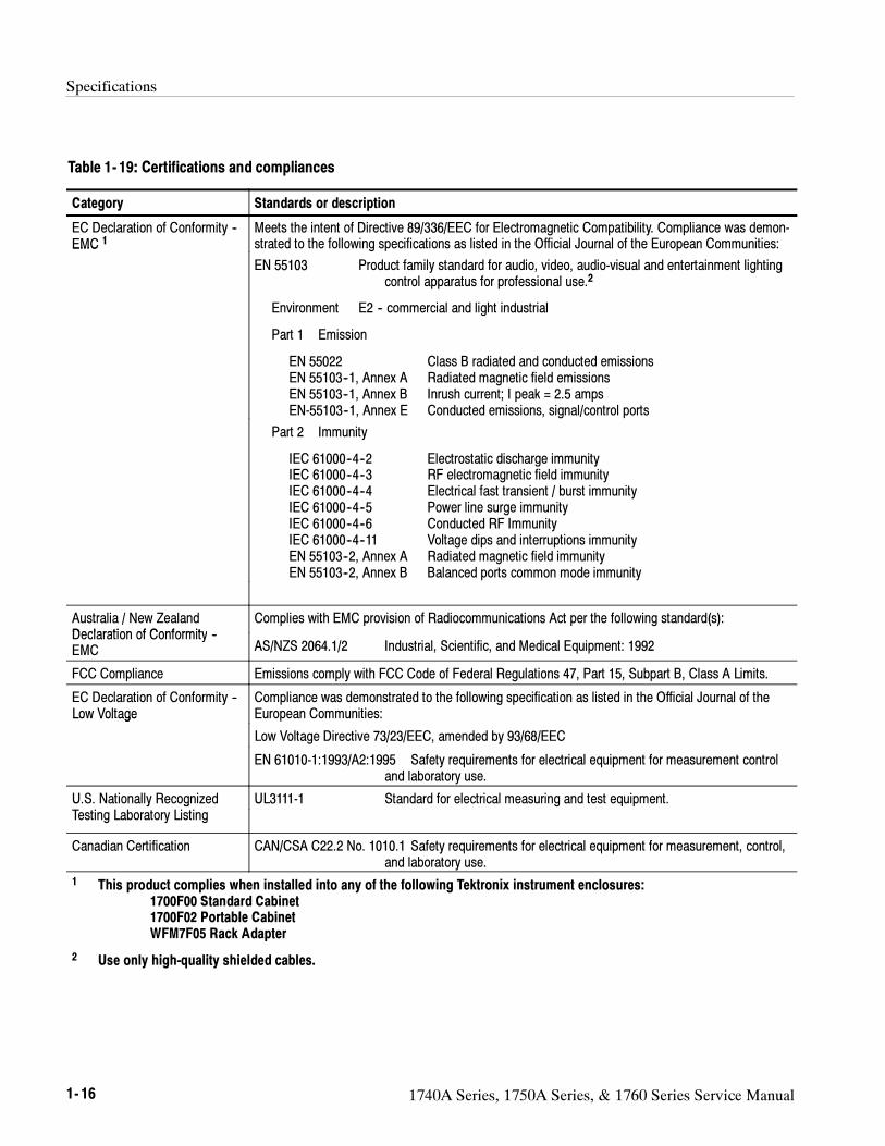
Table 1- 19: Certifications and compliances
Category Standards or description
EC Declaration of Conformity --EMC 1
Meets the intent of Directive 89/336/EEC for Electromagnetic Compatibility. Compliance was demon-strated to the following specifications as listed in the Official Journal of the European Communities:EMC
EN 55103 Product family standard for audio, video, audio-visual and entertainment lightingcontrol apparatus for professional use.2
Environment E2 -- commercial and light industrial
Part 1 Emission
EN 55022 Class B radiated and conducted emissionsEN 55103--1, Annex A Radiated magnetic field emissionsEN 55103--1, Annex B Inrush current; I peak = 2.5 ampsEN-55103--1, Annex E Conducted emissions, signal/control ports
Part 2 Immunity
IEC 61000--4--2 Electrostatic discharge immunityIEC 61000--4--3 RF electromagnetic field immunityIEC 61000--4--4 Electrical fast transient / burst immunityIEC 61000--4--5 Power line surge immunityIEC 61000--4--6 Conducted RF ImmunityIEC 61000--4--11 Voltage dips and interruptions immunityEN 55103--2, Annex A Radiated magnetic field immunityEN 55103--2, Annex B Balanced ports common mode immunity
Australia / New ZealandDeclaration of Conformity
Complies with EMC provision of Radiocommunications Act per the following standard(s):Declaration of Conformity --EMC AS/NZS 2064.1/2 Industrial, Scientific, and Medical Equipment: 1992
FCC Compliance Emissions comply with FCC Code of Federal Regulations 47, Part 15, Subpart B, Class A Limits.
EC Declaration of Conformity --Low Voltage
Compliance was demonstrated to the following specification as listed in the Official Journal of theEuropean Communities:Low Voltage
Low Voltage Directive 73/23/EEC, amended by 93/68/EEC
EN 61010-1:1993/A2:1995 Safety requirements for electrical equipment for measurement controland laboratory use.
U.S. Nationally Recognized UL3111-1 Standard for electrical measuring and test equipment.y gTesting Laboratory Listing
Canadian Certification CAN/CSA C22.2 No. 1010.1 Safety requirements for electrical equipment for measurement, control,and laboratory use.
1 This product complies when installed into any of the following Tektronix instrument enclosures:1700F00 Standard Cabinet1700F02 Portable CabinetWFM7F05 Rack Adapter
2 Use only high-quality shielded cables.

Specifications
1740A Series, 1750A Series, & 1760 Series Service Manual 1- 17
Table 1- 19: Certifications and compliances (cont.)
Category Standards or description
Additional Compliance IEC61010-1 Safety requirements for electrical equipment for measurement, control, andlaboratory use.
ISA S82.02.01:1999 Safety standard for electrical and electronic test, measuring, controlling, andrelated equipment.
Installation (Overvoltage)Category Descriptions
Terminals on this product may have different installation (overvoltage) category designations.The installation categories are:Category Descriptions
CAT III Distribution-level mains (usually permanently connected). Equipment at this level istypically in a fixed industrial location.
CAT II Local-level mains (wall sockets). Equipment at this level includes appliances, portabletools, and similar products. Equipment is usually cord-connected.
CAT I Secondary (signal level) or battery operated circuits of electronic equipment.
Pollution Degree Descriptions A measure of the contaminates that could occur in the environment around and within a product.Typically the internal environment inside a product is considered to be the same as the external.Products should be used only in the environment for which they are rated.
Pollution Degree 1 No pollution or only dry, nonconductive pollution occurs. Products in thiscategory are generally encapsulated, hermetically sealed, or located in cleanrooms.
Pollution Degree 2 Normally only dry, nonconductive pollution occurs. Occasionally a temporaryconductivity that is caused by condensation must be expected. This location isa typical office/home environment. Temporary condensation occurs only whenthe product is out of service.
Pollution Degree 3 Conductive pollution, or dry, nonconductive pollution that becomes conductivedue to condensation. These are sheltered locations where neither temperaturenor humidity is controlled. The area is protected from direct sunshine, rain, ordirect wind.
Pollution Degree 4 Pollution that generates persistent conductivity through conductive dust, rain,or snow. Typical outdoor locations.
Equipment type Test and Measurement
Safety Class Class I
Overvoltage Category CAT II
Pollution Degree Pollution Degree 2

Specifications
1- 18 1740A Series, 1750A Series, & 1760 Series Service Manual

1740A Series, 1750A Series, & 1760 Series Service Manual 2- 1
Installation
The information contained here deals with the installation and operation of the1740A/1750A/1760--Series instrument. If the instrument is to be removed fromits installed position for servicing, this will provide the information needed toremove it or reinstall it. Note that the repackaging information is located at theend of the Maintenance section.
Standard Accessories
This instrument is shipped with a set of standard accessories. These are the itemsnecessary to place the instrument in service, such as the power cord. When thebox for the instrument is opened, it should contain:
One User Manual.
Power cord assembly (See Options)
One cartridge fuse.
Three replacement graticule light bulbs.
Three replacement air filters
Two 3.5-inch high density disks are included with this manual. The disks run onan IBM compatible PC with a DOS 3.3 or higher operating system and a3.5-inch high-density disk drive.
One disk contains the current operating software for the instrument. To deter-mine the level of software loaded in an instrument, perform the following steps:
1. Power up the 1740A/1750A/1760--Series.
2. Push the CONFIG menu button.
3. Select the REMOTE submenu.
4. Read the software version number from the lower right corner of the CRT.
The other disk contains the procedure needed to return the instrument operationto its specified levels. This procedure works in conjunction with the AdjustmentProcedures section of this manual. Version 2.2 or higher software must be loadedin the instrument to use the Adjustment procedures.

Installation
2- 2 1740A Series, 1750A Series, & 1760 Series Service Manual
Mechanical Installation
Rear
6.130
Bottom Side
12.725
8.250
6.8750.688
1.060
16.180
5.105
0.156 Diameter (4)
Figure 2- 1: Dimensions of the 1700F00 plain cabinet
The cabinets available for this instrument provide necessary shielding andprotection against accidental electrical shock, and also protect internal circuitryagainst build up of dust. A supply of filtered, cooling air is provided from therear panel and exits through the cabinet vent holes. Operation in air flowrestricted environments may lead to excessive heat build up.
All qualification testing for the 1740A/1750A/1760--Series instruments wasperformed in a 1700F00 cabinet. To guarantee compliance with specifications,the instrument should be operated in a cabinet. The plain cabinet, 1700F00, isshown in Figure 2--1.
Also available are the 1700F02 Portable carrying case and the WFM7F05side-by-side rack mount assembly. All of these cabinets are available fromTektronix. If you need one of these cabinets, contact your nearest Tektronix fieldoffice or representative for assistance in ordering.
Cabinets

Installation
1740A Series, 1750A Series, & 1760 Series Service Manual 2- 3
3.310
Bottom Side
16.1809.435
0.141 Diameter (4)5.0001.625
Rear
8.250
6.8750.688
5.105
Figure 2- 2: 1700F02 portable cabinet
The portable cabinet, 1700F02, is shown in Figure 2--2. The 1700F02 has ahandle, four feet, a flip-up stand. The mounting hole sizes and spacing aredifferent from those of the 1700F00.
The 1700F00, 1700F02, and WFM7F05 cabinets, which are available fromTektronix as optional accessories, provide the proper electrical environment forthe instrument. They supply adequate shielding, minimize handling damage, andreduce dust accumulation within the instrument.

Installation
2- 4 1740A Series, 1750A Series, & 1760 Series Service Manual
CAUTION. Do not attempt to carry an instrument in the cabinet without installing
the mounting screws. Without the mounting screws, there is nothing to hold the
instrument in the cabinet if it is tipped forward.
The instrument is secured to the cabinet by two 6-32 Pozidrive screws, locatedin the upper corners of the rear panel. See Figure 2--3.
Cabinet securing screws
Figure 2- 3: Rear view showing the securing screws
The optional WFM7F05 side-by-side rack adapter, shown in Figure 2--4, consistsof two attached cabinets. It can be used to mount the 1740A/1750A/1760--Seriesand another half-rack width instrument in a standard 19-inch rack.
CAUTION. Be sure to read and follow the instructions that are shipped with the
rack adapter.
Use the correct sleeve for your product. The ventilation holes and EMI shielding
on the sleeves are specially designed to meet the requirements of the instruments
for which they were intended. If you use the wrong sleeve, it could damage the
instrument and cause overheating problems.
When working with instruments that are not enclosed in a chassis, you must
observe static precautions. You must also be careful not to damage circuit board
mounted components or interconnection wiring when sliding a sleeve over these
products.
Installing the Cabinet
Rack Adapter

Installation
1740A Series, 1750A Series, & 1760 Series Service Manual 2- 5
18.970
5.250
17.270
Controls front panelto rack alignmentRear view
6.875
Mountingholes
Figure 2- 4: The WFM7F05 side-by-side rack adapter
The rack adapter is adjustable, so the instrument can be more closely alignedwith other equipment in the rack. See Figure 2--4.
WFM7F05
1700F06
Figure 2- 5: A WFM7F05 with a blank front panel (1700F06)

Installation
2- 6 1740A Series, 1750A Series, & 1760 Series Service Manual
If only one side of the rack adapter is used, a 1700F06 Blank Panel can beinserted in the unused section. See Figure 2--5. The rack adapter and panel areavailable through your local Tektronix field office or representative.
When only one instrument is mounted in the side-by-side adapter, an accessorydrawer (1700F07) can be installed in the blank side of the cabinet. SeeFigure 2--6.
1700F07
WFM7F05
Figure 2- 6: WFM7F05 rack mount cabinet with a 1700F07 utility drawer

Installation
1740A Series, 1750A Series, & 1760 Series Service Manual 2- 7
For applications such as consoles, the instrument can be mounted with frontmolding flush or protruding from the console. In both cases, allow approximate-ly 3 inches of rear clearance for BNC and power-cord connections.
To mount the instrument safely, attach it to a shelf strong enough to hold itsweight. Install the mounting screws through the four 0.156-inch diameter holesin the bottom of the 1700F00 cabinet. See Figure 2--7.
Requires four 0.156” holes belowthe 1700F00 cabinet to secure
the instrument to the shelf.
For flush front panel: Cut hole thesame size as the monitor front moldingto allow the monitor front panel to align
with the custom panel surface.
For protruding front molding:Cut hole in panel the same size as theopening in the monitor cabinet to allow
the front panel molding to cover the hole.
Figure 2- 7: Custom installation of an instrument
Custom Installation

Installation
2- 8 1740A Series, 1750A Series, & 1760 Series Service Manual
Electrical Installation
These monitors are designed to operate from a single-phase power source havingone of its current-carrying conductors at or near earth ground (the neutralconductor). Only the line conductor is fused for over-current protection Systemsthat have both current-carrying conductors live with respect to ground (such asphase-to-phase on multiphase systems) are not recommended as power sources.A protective ground connection by way of the grounding conductor in the powercord is essential for safe operation.
WARNING.When power is supplied, line voltage will be present in the instru-
ment, even if the POWER switch is set to STANDBY.
The 1740A/1750A/1760--Series monitors operate at 50 and 60 Hz, over the rangeof 90--250 Volts, without operator adjustment.
These instruments ship with a standard North America power cord, unless apower cord option was ordered. Table 7--1 in the Options section shows theavailable options.
No operational modifications are made to this monitor through internal jumpersettings.
Power Source
Mains Frequency andVoltage Range
Power Cord Options
Operational Changes

Installation
1740A Series, 1750A Series, & 1760 Series Service Manual 2- 9
Rear Panel Connectors
Signals into and out of the instrument are connected via the rear panel. Videosignals are input/output through the BNC connectors, except for the RGBstaircase signal which is input through the REMOTE connector. Generalinformation about the rear panel connectors is provided in the followingparagraphs. Figure 2--8 shows the rear panel configuration for a 1760--Seriesinstrument. The only difference between the 1760--Series rear panel and the otherinstrument rear panels is the presence of the GBR outputs.
REMOTE
75 OHM LOOP-THROUGH COMPENSATED
RS232
EXT
REF
PIX
OUT
B
G
R
A3 A2 A1 A
B3 B2 B1 B
5 1 13 1
9 6 25 14
Figure 2- 8: Rear panel connectors
There are a total of eight 75 Ω compensated loop-through video input BNCconnectors. These inputs are not internally terminated; inputs require 75 Ω
external termination to provide accurate measurement capabilities. Inputs A andB are dedicated composite inputs regardless of instrument type. InputsA1--A2--A3 and B1--B2--B3 can also be used as composite inputs, but ifcomponent signals are to be displayed, they become the component inputs.
Maximum operating input voltage for all inputs is --1.8 V to +2.2 V DC pluspeak AC. Absolute maximum input voltage is --8.5 V to +8.5 V DC pluspeak AC.
The external reference input provides both external synchronizing signals andexternal subcarrier input to these instruments. Input is either black burst orcomposite video. It is a 75 Ω compensated loop-through input, requiring externaltermination.
75 Ω Loop-ThroughVideo Inputs
External Reference(EXT REF)

Installation
2- 10 1740A Series, 1750A Series, & 1760 Series Service Manual
The PIX OUT is a 75 Ω, nonfiltered output designed to drive a picture monitor.A bright-up strobe is added when the instrument is operated in the line selectmode. Strobe will either be the line in the selected field, the line in all fields orof 15 lines duration in the selected field or all fields. In the 15-line mode, thebright up starts with the selected line.
1760--Series Only. These three 75 Ω outputs are from the color difference-to-GBR transcoder. When the input is RGB, the transcoder is bypassed. The G(green) output contains sync.
Remote Connector
The rear-panel REMOTE connector is a 25-pin, D-type connector. It provides theinput for stereo L and R audio. TTL signal or ground closure to designated pinsare the enables. Eight front-panel setups can also be stored and recalled throughthe Remote connector. Table 2--1 shows pin assignments and Figure 2--9 showsthe connector.
REMOTE !
113
1425
Figure 2- 9: Rear panel REMOTE connector.
Picture Monitor Out(PIX OUT)
GBR Output

Installation
1740A Series, 1750A Series, & 1760 Series Service Manual 2- 11
Table 2- 1: Remote connector
Pin number Function Signal requirement Miscellaneous information
1 RGB/YRGB Staircase Input
External Horiz. Input
+10 V for RGB/YRGB
0 -- +5 V Sawtooth
≈9 divisions of sweep. (Staircase/external horizontal andRGB/YRGB selected through the menu.)10 divisions of horizontal deflection.
2 Ground
3 Staircase/Ext. Horiz. Enable Ground (TTL low) Grounding enables the function. (Staircase or external horizontalselected through the menu.)
4 External Blanking Input Negative-going signal Enabled by menu selection.
5 Remote Sync Input TTLlevel square wavetriggers 2-field sweep.
30/90 Hz for NTSC25/100 Hz for PAL
6 Remote Sync Enable Ground (TTL low) Grounding enables the function.
7 Ground
8 +Y Audio Input Max. Input±8 V peak. Left in phase. Measured to Chassis Ground.
9 --Y Audio Input Max. Input±8 V peak. Left out of phase. Measured to Chassis Ground.
10 +X Audio Input Max. Input±8 V peak. Right in phase. Measured to Chassis Ground.
11 --X Audio Input Max. Input±8 V peak. Right out of phase. Measured to Chassis Ground.
12 + Time Code Input --10 -- +10 V peak. Longitudinal Time Code, differential.
13 -- Time Code Input --10 -- +10 V peak. Longitudinal Time Code, differential.
14 Ground
15 & 16 Not used
17 Preset 1 Ground (TTL low) Ground pin 17 to recall front-panel setup from preset 1. Groundpins 17 and 25 to store current front-panel setup at preset 1.
18 Preset 2 Ground (TTL low) Ground pin 18 to recall front-panel setup from preset 2. Groundpins 18 and 25 to store current front-panel setup at preset 2.
19 Preset 3 Ground (TTL low) Ground pin 19 to recall setup from preset 3. Ground pins 19 and25 to store current setup at preset 3.
20 Preset 4 Ground (TTL low) Ground pin 20 to recall setup from preset 4. Ground pins 20 and25 to store current setup at preset 4.
21 Preset 5 Ground (TTL low) Ground pin 21 to recall setup from preset 5. Ground pins 21 and25 to store current setup at preset 5.
22 Preset 6 Ground (TTL low) Ground pin 22 to recall setup from preset 6. Ground pins 22 and25 to select preset 6 as storage location for current setup.
23 Preset 7 Ground (TTL low) Ground pin 23 to recall setup from preset 7. Ground pins 23 and25 to select preset 7 as storage location for current setup.

Installation
2- 12 1740A Series, 1750A Series, & 1760 Series Service Manual
Table 2- 1: Remote connector (Cont.)
Pin number Miscellaneous informationSignal requirementFunction
24 Preset 8 Ground (TTL low) Ground pin 24 to recall setup from preset 8. Ground pins 24 and25 to select preset 8 as storage location for current setup.
25 Store Ground (TTL low) Ground this pin along with one of the Preset pins to store thecurrent front-panel setup at the selected Preset location.
Remote Connector Converter
If the 1740A/1750A/1760--Series replaces a 1740/1750--Series instrument, rewirethe remote cable or provide an adapter as shown in Figure 2--10
If the 1740A/1750A/1760--Series replaces an Option 16 instrument, construct theadapter in the same manner, omitting the pin 3-to-pin-25 connection.
114
1325
Remote plug
*(Do not connect when replacing Option 16 instruments.)
8
1
14
1325
3
5
GROUND7
6
19
10
9
REMOTE SYNC ENABLE
REMOTE SYNC IN
RGB ENABLE*
RGB INPUT
1740A/1750A/1760--Seriesrear-panel REMOTE connector
Figure 2- 10: Replacement adapter for 1740/1750

Installation
1740A Series, 1750A Series, & 1760 Series Service Manual 2- 13
RS232 Connector
This 9-pin subminiature D-type connector provides a serial interface for remotecontrol. It has a driver built in for RS232 serial binary data interchange. Theoperational mode is full duplex. Data rate = 9600 baud; data type is asynchro-nous. Figure 2--11 shows pin assignments and connector orientation.
1 DCD2 Receive Data (RxD)3 Transmit Data (TxD)4 Data Terminal Ready (DTR)5 Signal Ground (GND)
5 4 3 2 1
9 8 7 6
RS232
6 Data Set Ready (DSR)7 Request to Send (RTS)8 Clear to Send (CTS)9 No connection
Figure 2- 11: Rear panel RS232 connector

Installation
2- 14 1740A Series, 1750A Series, & 1760 Series Service Manual
Installing Software
These versatile monitors can be upgraded to perform additional measurements orto revise operations. Software code is contained in Flash EPROM that can bewritten over when upgrades become available.
If you replace the Flash EPROM, you must reinstall the software from thesoftware disk accompanying this manual.
To find the current version of software, go to the CONFIG menu and then to theREMOTE submenu. The version number, preceded by the letter V, is displayedin the lower right corner of the screen.
The software disk is a 3.5” (1.44MB) high-density disk. It contains all programsnecessary to upgrade or reload the operating software in the Tektronix1740A/1750A/1760--Series instruments. If a disk drive other than 3.5” is to beused, copy the contents of the disk to the desired size disk or to a hard diskdirectory. The disk contents are:
NVSAVE.EXE. Saves calibration constants and user presets.
CONVERT.EXE.Updates format of calibration and preset data.
UPGRADE.EXE. Performs software upgrade.
NVRESTOR.EXE. Restores calibration constants and user presets.
NEW_CAL.EXE. Used to calibrate new features.
SOFTWARE.BIN. Data file used by UPGRADE.EXE.
IBM Compatible PC with the following
DOS 3.3 or Higher.
640 K Bytes Random-Access Memory (RAM).
High Density Floppy Drive (3.5”/1.44 MB).
Available RS232 Port (COM 1, 2, 3, or 4).
RS232 Cable to connect PC to the 1740A/1750A/1760--Series RS232connector.
Software Disk
Required Equipment
Installation
1740A Series, 1750A Series, & 1760 Series Service Manual 2- 15
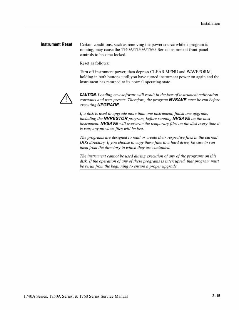
Certain conditions, such as removing the power source while a program isrunning, may cause the 1740A/1750A/1760--Series instrument front-panelcontrols to become locked.
Reset as follows:
Turn off instrument power, then depress CLEAR MENU and WAVEFORM,holding in both buttons until you have turned instrument power on again and theinstrument has returned to its normal operating state.
CAUTION. Loading new software will result in the loss of instrument calibration
constants and user presets. Therefore, the program NVSAVE must be run before
executing UPGRADE.
If a disk is used to upgrade more than one instrument, finish one upgrade,
including the NVRESTOR program, before running NVSAVE on the next
instrument. NVSAVE will overwrite the temporary files on the disk every time it
is run; any previous files will be lost.
The programs are designed to read or create their respective files in the current
DOS directory. If you choose to copy these files to a hard drive, be sure to run
them from the directory in which they are contained.
The instrument cannot be used during execution of any of the programs on this
disk. If the operation of any of these programs is interrupted, that program must
be rerun from the beginning to ensure a proper upgrade.
Instrument Reset

Installation
2- 16 1740A Series, 1750A Series, & 1760 Series Service Manual
Loading Software
PC Hookup Hook up the 1740A/1750A/1760--Series rear-panel RS232 connectorto the COM 1, 2, 3, or 4 connector on the PC, as shown in Figure 2--12 or Figure2--13. If pins two and three (RXD and TXD) are swapped, as in some MODEMconnections, the upgrade will not operate.
16
5
1
6
9 5 Signal ground
9-Pin femaleconnector to PC
9-Pin male connector to1740A/1750A/1760-Series
9
1
6
9 5 Signal ground
9-Pin femaleconnector to PC
9-Pin male connector to1740A/1750A/1760-Series
1
6
95
1 DCD2 Receive Data (RxD)3 Transmit Data (TxD)4 Data Terminal Ready (DTR)5 Signal Ground (GND)6 Data Set Ready (DSR)7 Request to Send (RTS)8 Clear to Send (CTS)9 No connection
Alternate hookup
Standard hookup
Figure 2- 12: Standard and alternate hookups for the 9-pin connector

Installation
1740A Series, 1750A Series, & 1760 Series Service Manual 2- 17
114
1325
2
3
4
5
16
95
7
9-Pin male connector to1740A/1750A/1760-Series
25-Pin femaleconnector to PC
2
3
820
Signal ground
6
114
1325
2
3
4
5
1
6
95
7
9-Pin male connector to1740A/1750A/1760-Series
25-Pin femaleconnector to PC
2
3
8
20
Signal ground
6
Standard hookup
4
7
8
Alternate hookup
Figure 2- 13: Standard and alternate hookups for 25-Pin PC Connector

Installation
2- 18 1740A Series, 1750A Series, & 1760 Series Service Manual
1. Run NVSAVE
(Execution time <1 minute)
a. Power on the 1740A/1750A/1760-Series instrument.
NOTE. PC Disk Drive or Hard Disk
On PCs, the drive letter for the disk drive may be A, B, etc. Enter the appropri-
ate letter for your disk drive in the following steps. If the disk contents were
copied to a hard disk directory, run the programs from that directory.
b. Insert disk into PC 3.5 inch disk drive.
CAUTION. In order to execute “NV SAVE”, the disk is not write protected . Do
not place it in write protect mode.
c. At the DOS prompt, type “B:” and ENTER.
d. Type “NVSAVE” and ENTER. When asked for the COM port, respond withthe number of the port you are using. (If you enter an incorrect portnumber, you will be prompted to try again.)
The program stores the following temporary files on the disk:CALS.TMP (calibration constants)PRESET.CUR (instrument’s current front-panel setup)PRESET.001--009 (user-defined presets)PRESET.FCT (factory-defined preset)
e. Wait for the message that the program execution is completed.
2. Run CONVERT
(Execution time <1 minute)
a. Type “CONVERT” and ENTER.
3. Prepare Waveform Monitor for Upgrade
a. Turn instrument power to STANDBY.
WARNING.When power is supplied, line voltage will be present in the instru-
ment, even if the POWER switch is set to STANDBY.
b. Move the plug jumper on J4 (Main board) to pins 1 and 2 (the pinsclosest to U14).
Procedure forLoading Software
Installation
1740A Series, 1750A Series, & 1760 Series Service Manual 2- 19
c. Set switch 4 of SW1 to the open position. (SW1 is the red switch on theMain board, near the front of the instrument.)
d. Turn on the instrument and allow it to boot (wait a few moments untilthe 1740A/1750A/1760-Series CRT and front-panel LEDs are illumi-nated as for normal operation).
4. Run UPGRADE(Execution time ¶12 minutes)
NOTE. If a power loss to either the PC or the 1740A/1750A/1760-Series occurs
during software loading, the instrument may lock up and not restart normally. If
this occurs, refer to the special recovery procedure on page 2--20.
a. Be sure that NVSAVE was executed (step 1).
b. At the DOS prompt, type “B:” and ENTER.
c. Type “UPGRADE” and ENTER. When asked for the COM port, respondwith the number of the connector you are using.
d. Wait for the message that the program execution is completed.
e. Turn off the 1740A/1750A/1760-Series instrument power.
f. Return the plug jumper to pins 2 and 3, and return #4 of SW1 to theclosed state.
g. Turn on instrument power to enable the new software.
5. Run NVRESTOR(Execution time <1 minute)
a. At the DOS prompt, type “B:” and ENTER.
b. Type “NVRESTOR” and ENTER. When asked for the COM port, respondwith the number of the port you are using.
c. Wait for the message that the program execution is completed.
d. Verify that step 4f has been performed.
e. This completes the Software Upgrade Procedure.

Installation
2- 20 1740A Series, 1750A Series, & 1760 Series Service Manual
Calibrating New Features
The new instrument features must be calibrated using the following procedure. Acolor bar signal is required.
1. Run NEW_CAL
a. After installing the new version software, with the RS232 cable stillattached and the instrument operating, type “NEW_CAL” and ENTER.
NOTE. Each time an adjustment is indicated in the following steps, type the given
letter on the PC keyboard, and then press the up/down or left/right keyboard
arrows as many times as required to achieve the described adjustment. The
arrows function as follows:→
large increase
←
large decrease
↑
small increase
↓
small decrease
2. Calibrate the new features.
a. Perform steps A through I for all instruments.
b. Perform steps J and K for 1760-Series.
c. Type X to exit the program.
Special Recovery for Power Loss During the Execution of UPGRADE
If there is a power failure to either the instrument or the PC while the software isloading, the following recovery procedure is necessary:
1. Turn the 1740A/1750A/1760-Series front-panel POWER switch to STAND-BY.
2. Start the PC upgrade procedure program and proceed through the menusuntil the SELECT COM PORT menu is on screen.
3. Type in the number of the COM PORT, but do not press RETURN.
4. Turn the 1740A/1750A/1760-Series front-panel POWER switch to ON.
5. Within 6 seconds, press RETURN on the PC.

1740A Series, 1750A Series, & 1760 Series Service Manual 2- 21
Operating Information
This section contains a brief introduction, minimal operating instructions,general menu information, an overview of the instrument functions, and briefinstructions for displaying the desired signal. Consult the user manual if youneed a more complete explanation.
Getting Started
You should be aware of the following special characteristics of the1740A/1750A/1760--Series:
Composite (NTSC or PAL) signals can be connected to any or all of theeight input channels. Three-channel component (for example, GBR or Y, PB,PR) signals should be connected to inputs A1--A2--A3 and B1--B2--B3. Selectthe CONFIG/INPUT display to configure the “A123” and “B123” inputs forthe type of signal you are monitoring.
Each type of Waveform display (one line, two line, one field, and two field)has one level of horizontal magnification that can be turned on and off withthe MAG button. The level of magnification depends on the display type;you can sequentially display the four magnified views by repeatedly pressingthe Line/Field SWEEP button (once SWEEP MAG has been selected).
The 1760--Series BOWTIE Display subtracts channels 2 and 3 fromchannel 1 and automatically displays the results in a parade format; when“A123” is selected, the A1 minus A2 waveform is shown to the left of theA1 minus A3 waveform. This lets you use the Tektronix-developed Bowtietest signal to check and adjust inter-channel timing on component systems.
The rear-panel REMOTE connector accepts audio signals. See Appendix Bof the user manual for the pin assignments.
The five buttons arranged vertically to the right of the display are calledBezel Buttons. Use these buttons to toggle or select on-screen menu options.
The middle three knobs under the display are called Bezel controls. Turnthese knobs to adjust the parameters (or scroll through the lists) that appearabove them on the display screen.

Operating Information
2- 22 1740A Series, 1750A Series, & 1760 Series Service Manual
Operating Instructions
1. Connect the instrument to the desired signal path(s). Remember to connectcomponent signals to A1--2--3 or B1--2--3. Be sure that all paths areterminated; add a termination to the loop-through connector, as necessary.
2. Plug the instrument in and switch it on. The On/Standby (POWER) switch ison the bottom right corner of the front panel.
3. Select the CONFIG menu with its front-panel button and adjust theparameters as required for your particular installation.
INPUT
MULTIPLE
DISPLAY
PARADE
OVERLAY
CH B3
CH A3
CH A2
CH B2
CH B1
CH A1
CH B
CH A
WAVEFORM
TIME CODE
MENUSWEEP
FILTER
CURSOR
LIN SEL
PRESET
CONFIG
GAIN
CRT
POWER
ON/STANDBY
LINE
FIELD
MAG
DC REST
RESTORE
REF
EXTCLEAR
WAVEFORM/
VECTOR MONITOR
PICTURE
VERT POS HORIZ POS
MENU
1760
SCH
VECTOR
LIGHTNING
BOWTIE
A 123
B 123
AUDIO
Figure 2- 14: 1760 front panel
4. Use the DISPLAY and INPUT buttons to view some aspect of the desiredsignal.
5. Select the CRT menu to adjust the waveform, readout, and scale brightness,and the waveform focus. Press the CLEAR MENU button to remove themenu from the display.
6. Use the front panel controls (Figure 2--14) to observe and measure thedesired signals. For more details, see the following pages or the user manual.

Operating Information
1740A Series, 1750A Series, & 1760 Series Service Manual 2- 23
General Menu Information
The next few paragraphs describe the general techniques for using the menus.
To get started, press a MENU button (on the far right of the front panel) to callup one of the menu readouts.
Menu selections appear along the right side of the screen. Descriptive labels,when present, appear in ITALIC text. Selections appear in Roman (standard) text,with the current selection outlined. Use the five bezel buttons along the right sideof the CRT to change the selections. Figure 2--15 shows the bezel controls andbuttons.
VERTPOS HORIZPOS
Bezel controls
CLEAR
MENU
Bezelbuttons
Left Center Right
DISPLAY
READOUT
TRACE
FOCUS SCALE INTENSITY
TEST
ON OFF
Figure 2- 15: The CRT menu, with the bezel controls and buttons
The center three controls under the CRT are referred to as Left, Center, and Rightbezel controls. Control functions vary with menu choice; a readout just aboveeach active knob shows its present function. The knobs are used as variableanalog controls to set values such as phase, amplitude, and intensity. The leftcontrol is also used to scroll and select categories within the CONFIG menu.
Selecting a second menu removes the present menu display, but the functionstypically remain active (with the menu LED remaining lighted to show thisstate). To reinstate a menu display, press that menu button again. CRT, PRESET,and CONFIG menus are exited completely when another menu button is pressed.
Multi-Use Bezel Controlsand Buttons
Moving Between Menus
Operating Information
2- 24 1740A Series, 1750A Series, & 1760 Series Service Manual
Press CLEAR MENU to clear part of the menu display, but leave essentialreadout elements such as control assignments and measurement readouts. (Themenu LED remains lighted to show this state.) Press the menu button to bringback the full display. CRT, PRESET, and CONFIG menus are exited completelywhen CLEAR MENU is pressed.
To exit a menu function while its display is present, press that menu button. (Themenu button functions as an on-off toggle switch). If the menu display is notpresent, but the menu function is still in effect (LED is lighted), press the menubutton to bring back the full display, then press it again to exit the menu.
Clear Menu
Exiting a Menu Function

Operating Information
1740A Series, 1750A Series, & 1760 Series Service Manual 2- 25
Functional Overview
The Functional Overview tells how to use your instrument to monitor a signal.To select a particular signal, see Displaying a Signal on page 2--27.
The displays that can be chosen for each type of signal are listed in Table 2--2and explained in the following paragraphs.
Table 2- 2: The available display modes
Mode Composite Component
Vector Yes 1760--Series only
SCH 1750A--Series & 1760--Series, Option SC only
Waveform Yes Yes
Audio Yes (using REMOTE input) Yes, using REMOTEinput
Lightning & Diamond 1760--Series only
Bowtie 1760--Series only
Picture Yes Yes
Time Code Yes Yes
Multiple Displays Yes Yes
The vector mode presents an XY plot of demodulated chrominance phase andamplitude. The angle represents chrominance phase and the distance from thecenter represents chrominance amplitude. A bezel control adjusts vector phase.
With a component input (A123 or B123), the vector display is channel 3(typically R--Y or PR) versus channel 2 (typically B--Y or PB).
SCH (the 1750A--Series and 1760--Series with option SC only) provides a vectordisplay of the subcarrier-to-horizontal-sync phase relationship. The burst vectorand the phase of the 50% point of the leading edge of sync are displayed.
Subcarrier-to-horizontal phase and color framing are displayed graphically in thepolar SCH display. Sync jitter over the field shows as a moving sync vector dot.You can verify correct color framing by the position of the single sync vector dotrelative to the color subcarrier vector when the monitor is externally referenced.
The SCH phase of the reference signal is separately sensed to allow reliable colorframing comparison. Using this method of determining relative color framing
Display Modes
Vector
SCH
Operating Information
2- 26 1740A Series, 1750A Series, & 1760 Series Service Manual
eliminates the requirement for a precise horizontal timing match between thereference and measured signals.
The waveform monitor portion of the instrument provides a voltage-versus-timedisplay of the video signal. The selected input can be displayed in one or twoline, or one or two field sweeps. In LINE SELECT mode, identified lines of anyfield can be selected and displayed. Multiple inputs can be displayed, or multiplefilters can be used on one input for signal analysis. TIME and VOLTAGEcursors can be activated and positioned for reference or measurement.
Audio amplitude and phase is monitored using a calibrated X/Y Lissajousdisplay. You can verify that the program audio will be properly reproduced onboth monaural and stereo receivers. Correct phasing between two audio channelsis verified by the direction of the display.
The front-panel LIGHTNING button is used for both the Lightning and theDiamond displays. Use the DISPLAY button on the CONFIG/FORMAT menu totoggle between the Lightning and Diamond displays. Press the front panelCLEAR MENU button to remove the menu from the screen.
Selecting Lightning mode forces the instrument to A123 input display; it can bechanged to B123 with the front-panel button.
NOTE. A123 (or B123) must be configured as a component input (through the
COMPONENT/INPUT menu) for proper LIGHTNING or DIAMOND display.
In BOWTIE mode (1760--Series only), the display is forced to a two line or fieldsweep and the A123 input is selected. The left half of the display shows CH-1minus CH-2 and the right half shows CH-1 minus CH-3. If the timing betweenchannels is matched, the centers of the bowties will be centered and not skewed.If CH-2 is delayed with respect to CH-1, the skew moves to the right. If CH-2 isadvanced with respect to CH-1, the skew moves to the left.
NOTE. A123 (or B123) must be configured as a component input (through the
COMPONENT/INPUT menu) for proper BOWTIE display.
The PICTURE mode allows the operator to verify the signal source. In PIC-TURE mode with LINE SELECT on, a bright-up marker identifies the selectedline in the picture.
Waveform
Audio
Lightning and Diamond(1760- Series only)
Bowtie
Picture

Operating Information
1740A Series, 1750A Series, & 1760 Series Service Manual 2- 27
Longitudinal time code is monitored in a frame-rate display to allow observationof amplitude, synchronization, and phase with respect to reference vertical sync.Synchronization is confirmed by the stationary display and time code phase isdetermined by horizontal position of the time code sync word on the CRT.
When MULTIPLE is pushed, WAVEFORM, VECTOR, and SCH (Option SConly) can be selected at the same time.
When exiting MULTIPLE, the instrument will return to the previous (non-MUL-TIPLE) display settings. When entering MULTIPLE again, the previousMULTIPLE display settings will be restored.
Displaying a Signal
The following paragraphs describe how to use the front-panel buttons to displayexactly the signal or signals you want.
There are eight rear-panel loop-through inputs, which may eliminate the need foran external routing switcher. The inputs can be displayed singly or in severaldifferent combinations.
Without PARADE or OVERLAY selected, only one input selection can be madeat a time. Each input channel button (including A123/B123 or SELA/SELB)toggles between A and B, and is cancelled when another input button is pressed.
With PARADE or OVERLAY selected, the input channels can be displayed incombination. Pressing an input channel button sequences through the labeledchannels, both, then off. Pressing another input button does not cancel thecurrent selection, but adds to it. To return to “single input” operation, press thePARADE/OVERLAY button until it is off (LED is no longer lighted).
Inputs A1--A2--A3 and B1--B2--B3 may be used either as inputs for three-wirecomponent signals, or inputs for three separate composite signals. (TheCONFIG/INPUTS menu settings must match the actual signal type.)
Selecting A123 provides a side-by-side display of the CH-A1, CH-A2, andCH-A3 inputs (B123 displays the CH-B1, CH-B2, and CH-B3 inputs).
When PARADE or OVERLAY is selected, A123 and B123 can be displayedtogether and in combination with other inputs. If both A123 and B123 areselected, the display will consist of a side-by-side display of channels A1, A2,and A3, overlaid with a side-by-side display of channels B1, B2, and B3.
Time Code
Multiple
Inputs
A123/B123
Operating Information
2- 28 1740A Series, 1750A Series, & 1760 Series Service Manual
Selecting PARADE independent of A123/B123 displays the input channels lastselected for PARADE, allowing a custom configuration of inputs. In PARADEmode, the LINE/FIELD button offers only two choices: one line and one field.
PARADE allows up to four channels to be displayed side-by-side. Additionalchannels will be overlaid.
OVERLAY superimposes the selected input signals. In OVERLAY mode, theLINE/FIELD button remains a four-way toggle, providing one line, two line, onefield, and two field displays.
Sweep buttons select the waveform sweep rate. LINE/FIELD toggles throughfour sweep rate selections: one line, two line, one field, and two field. InPARADE mode, the LINE/FIELD button becomes a two-way switch, togglingbetween line and field.
The MAG button is used with LINE/FIELD to provide horizontal magnificationof each rate as follows:
One line magnified = 200 ns/division
Two line magnified = 1 µs/division
One field or two field magnified = approximately X20 magnification.
Parade
Overlay
Sweep

1740A Series, 1750A Series, & 1760 Series Service Manual 3- 1
Block Diagram Description
The 1740A Series of monitors provides the typical composite displays used tomonitor video quality. The 1750A Series adds SCH phase measurements. The1760 Series provides both composite and component analog capabilities.Option SC added to the 1760 Series provides SCH phase measurements.
The three block diagrams discussed here are located in the Diagrams and Circuit
Board Illustrations, at the rear of this volume. Circuits shown on a diagonalpatterned background are not present in the 1740A Series instruments; these arethe unique circuits for the 1750A Series and the 1760 Series.
Signal flow, microprocessor-generated levels, and feedback lines are shown assolid lines. Control lines are shown as dashed lines. Signal flow is from left toright on these diagrams.
Block Diagram 1: Input and Waveform Monitor
There are eight identical clamped input amplifiers. Their gain is approximatelyunity. They are of the bridging loop-through type and are compensated for 75Ωcharacteristic input impedance. All inputs are active and a multiplexer is used toselect signals for display. All three instrument series can accept both compositeand component inputs. Input coupling can be either ac or dc as selected from theConfigure menu. Clamp timing and clamping point are selected in the samemanner. Coupling and clamping selections are for all inputs; they cannot beindividually changed.
The Input Multiplexer provides the means to select the input signal for display.Selection of signals is controlled by the Line Rate Controller in response to frontpanel switch selections. The choices are: a single input, a parade of three inputs,or an overlaid display of the same three inputs. Overlay display is at the selectedline or field rate. Parade display is three consecutive lines or fields beginningwith the A1 or B1 input signal followed by A2 or B2 and A3 or B3.
In addition to driving the Input Multiplexer the video signal also drives theHorizontal Reference Multiplexer to select the internal sync and subcarrierreferences for the Line Rate Controller, chroma for the vectorscope, and SCHPhase.
The Internal/External Reference switch selects either the internal video or theexternal reference input as the instrument sync and subcarrier reference. Both theMultiplexer and the Reference Switch are controlled by outputs from the LineRate Controller.
Input Amplifier, Clamp,and Input Selection
Horizontal ReferenceMultiplexer and Reference
Switch

Block Diagram Description
3- 2 1740A Series, 1750A Series, & 1760 Series Service Manual
The Input Multiplexer drives both the Picture Monitor Out (Pix Out) and thechrominance and luminance filters. The filters can be bypassed to provide anunfiltered (Flat) display. The Pix Out signal, with or without line select bright up(strobe), is the buffered, unprocessed input signal from the Input Multiplexer.The Pix Out has a characteristic output impedance of 75Ω to match the inputimpedance of picture monitors.
In addition to removing chrominance for the displayed video, the LuminanceFilter drives the Diff Step Filter, and an input to the Horizontal Amplifier wherethe monochrome Pix Mon intensity signal is derived.
There are chrominance filters for both of the color standards that filter both theinput video signal and the output of the FSC Oscillator. The FSC Oscillatorgenerates the test circle for the vectorscope. Output of the appropriate colorstandard Chroma Filter is selected by a microprocessor-generated switchingsignal. The chrominance signal is routed through the Vertical Amplifier, isbuffered, and drives the vectorscope Chroma Amplifier.
The calibrator provides a 1 volt, 100 kHz output. Its amplitude is controlled bythe microprocessor and its timing is set by the Line Rate Controller.
The Auxiliary Switching, controlled by the Line Rate Controller extends thenumber of signals that can be input to the Filter Selection Multiplexer. Inaddition to being an input to the Auxiliary Switching the differential time codeinput is recovered, buffered, and output to the microprocessor which generatestime code display synchronizing signals.
The Filter Selection Multiplexer selects one of seven inputs, including theAuxiliary Switching, to be displayed. The vectorscope R--Y and the componentvertical signal outputs are input through this multiplexer.
The Vertical Amplifier is a variable gain amplifier that has controlling inputsdriven by either microprocessor or synchronous Line Rate Controller outputs.Stage gain is controlled by the microprocessor-generated DAC converted controlvoltages. Magnification is switched by a signal from the Line Rate Controller.An offset voltage from the DACs vertically positions the display.
When the CRT readout is being processed, the Line Rate Controller changes thegain of the amplifier. The differential output of the Vertical Amplifier drives thevertical output amplifier to normalize signal amplitude and drive the CRTdeflection plates.
An additional internal amplifier stage provides a chrominance differential outputto drive the vector chroma amplifier. Gain of the chrominance signal is con-trolled by the microprocessor.
Pix Out, Filters, andCalibrator
Auxiliary Switching
Filter Selection Multiplexer
Vertical Amplifier

Block Diagram Description
1740A Series, 1750A Series, & 1760 Series Service Manual 3- 3
Line and Field Rate signal generators are started and stopped by the retracesignals from the Line Rate Controller. Sweep ramp run up times ≈17 ms for thefield sweep and 64 s for the line sweep are controlled by the microprocessor.
The Horizontal Signal Multiplexer is controlled by the Line Rate Controller toselect a signal to drive the horizontal circuitry. The vectorscope B--Y and thecomponent horizontal signal outputs are input through this multiplexer.
The Horizontal Amplifier is a variable gain amplifier with controlling inputsfrom either the microprocessor or the Line Rate Controller. Stage gain iscontrolled by the microprocessor-generated control voltages. Magnification isswitched by a signal from the Line Rate Controller.
An offset voltage horizontally positions the display. The amount of positioningoffset required for the Waveform mode is significantly greater than that requiredfor the other display modes; therefore, a separate offset is required. When CRTreadout is being processed the gain of the amplifier is changed by the ReadoutSelect signal from the Line Rate Controller.
The differential output of the Horizontal Amplifier drives the horizontal outputamplifier to normalize signal amplitude and drive the CRT deflection plates.
An additional amplifier stage within the Horizontal Amplifier provides adifferential output that controls the intensity for the Picture Monitor mode.Picture Monitor contrast is controlled by the microprocessor.
The Blanking Logic is a multiplexer that is controlled by the Line RateController. It selects the blanking/unblanking signals that drive the Z--AxisAmplifier, which drives the CRT control grid.
Block Diagram 2: Vector - SCH - Component
The vector circuits on this page are common to all monitors of this family. TheSCH circuitry, in the upper left corner, is used by the 1750A Series and the1760 Series Option SC. Component circuits located in the lower right corner ofthis page are used only by the 1760 Series.
Chrominance from the incoming video signal, either internal or from the externalreference, is conditioned by a chrominance amplifier and input to the PhaseDetector at burst time. The chrominance input to the Lock Detector is delayed by90° and compared to the regenerated subcarrier, from the VCO, with the outputlow pass filtered and buffered. The resulting signal is a pulse, when burst ispresent, that clamps the Phase Detector output. It is also checked for phase lockand, if unlocked, an output is supplied to the Error Amplifier to increase itsbandwidth for faster locking.
Sweep Generators andHorizontal Signal
Multiplexer
Horizontal Amplifier
Blanking Logic
Subcarrier Regeneratorand Phase Shifter

Block Diagram Description
3- 4 1740A Series, 1750A Series, & 1760 Series Service Manual
When the Calibrator (Cal Sig On) is selected (from the Configure menu in Vectormode) the Error Amplifier is forced into an unlocked state to provide the testcircle. The regenerated subcarrier output by the VCO can be phase shifted up to360° by a digital phase shifter whose output is buffered and input to thedemodulators.
These instruments employ quadrature demodulation, which consists of delayingthe regenerated subcarrier by 90° to the R--Y (U) Demodulator. The incomingchrominance is compared to the regenerated subcarrier and the output is low passfiltered and amplified. Center dot clamping is used to keep the effects ofchrominance from distorting the display center dot.
For PAL signals the regenerated subcarrier is switched between + and -- inputs ofthe R--Y (U) Demodulator to accommodate the 180° phase shift betweensubsequent lines. When +V is selected the V--Axis switcher clamps oneregenerated subcarrier input of the R--Y (U) demodulator to ground to forcedemodulation on a single phase and disable the PAL switching.
A regenerated subcarrier signal is phase locked to the 50% point of sync. Thesubcarrier is then demodulated to produce an on-screen dot display in avectorscope-type presentation. Actual SCH phase is determined by measuringthe dot displacement from the displayed burst vector.
The 50% Detectors compare levels at backporch (burst gate) and sync tip tooutput transitions coincident with a point half way between the back porch andthe sync tip. The 4 x FSC oscillator is harmonically locked to the transition fromthis 50% point detector. The resultant output for internal reference is a propeller(2 SCH dots 180° apart) display. When color framing of two signals is needed anexternal reference signal is required.
The display logic is developed by comparing incoming reference video SCH andsync and then comparing the result to the subcarrier generated by the 4 x FSCOscillator, providing a single dot display. The relationship of the two subcarriersis determined by measuring the displacement of the SCH dot from the burstvector.
Output of the CH1, 2, and 3 (either A or B) Input Amplifiers drives theComponent input switching matrix. Switch output is buffered and becomes theCH1, CH2, and CH3 inputs to the Component display mode switching.
The three channel outputs drive both the Component Display mode switchingmatrix and the Color Difference to GBR Transcoder. Either a GBR input signalor the transcoded color difference signal can be buffered to drive the back porchclamped GBR Output Amplifiers. GBR outputs are compensated in 75Ω.
Demodulators
SCH(1750A- Series &
1760 Series Opt. SC only)
Component InputSwitching and Amplifier
(1760 Series only)
Color Difference to GBRTranscoder and GBR
Outputs(1760 Series only)

Block Diagram Description
1740A Series, 1750A Series, & 1760 Series Service Manual 3- 5
GBR signals from the Color Difference to GBR Transcoder are input to the GBRto Diamond Transcoder to be matrixed and applied to the Component Modeswitching. The outputs from the Transcoder are 0.5 times G+B or R or B--G.These outputs drive the vertical and horizontal axes for the diamond display.Mode switching provides the inputs to the axes for Lightning, Diamond,Component Vector, and Bowtie displays.
The Vertical Output Amplifier is a backporch clamped differential amplifier withunity gain. Its output is low-pass filtered (1.5 MHz) for all display modes exceptBowtie, which bypasses the filter. The Horizontal Output Amplifier is abackporch clamped buffer whose output is low-pass filtered (1.5 MHz). Theoutputs of both the amplifiers are input into the Output Amplifier Switching. Inaddition, the output of the Horizontal Amplifier drives the transition intensifierthat causes the Z--Axis to brighten enough to make the vector and lightningtransitions clearly visible.
Block Diagram 3: Microprocessor and Line Rate Controller
The heart of these instruments is a microprocessor. It controls all aspects of theinstruments operation. Where synchronous control signals are required a LineRate Controller is employed.
The 16-bit microprocessor has its program code stored in a Flash ErasableProgrammable Read-Only Memory (EPROM). The nonVolatile Random AccessMemory (NOVRAM) stores all of the constants used by the microprocessor. TheRandom Access Memory (RAM) is used to move system level code forexecution by the microprocessor. The Read-Only Memory (ROM) containsmicroprocessor code that is output on the 8 most significant bits to the data bus.
The Address Buffer is unidirectional to select the addresses in the storagedevices (RAM, ROM, and EPROM) while the Data Buffer is bidirectional fortwo-way communication with the storage devices.
The control circuitry for the component circuit board (1760--Series) is controlledby the microprocessor.
The Line Rate Controller is loaded from the microprocessor, synchronized to theincoming video reference, and outputs the synchronous switching signals that arerequired to make the displays viewed on the CRT.
Two sync separators time the line rate controller. One strips sync from theinternal video signal, while the second strips sync from the external referencevideo. Two separators are required to support color field identification (SCH).
GBR to DiamondTranscoder and Mode
Switching(1760 Series only)
Horizontal and VerticalComponent Outputs(1760 Series only)
Microprocessor
Component
Line Rate Controller
Sync Separators

Block Diagram Description
3- 6 1740A Series, 1750A Series, & 1760 Series Service Manual
Data from the microprocessor is loaded into latches that are clocked by the LineRate Controller to lock their outputs to the incoming video signal.
The Readout State Machine interprets the readout instructions from themicroprocessor and loads digital data into the DAC. Analog output of the DACdrives the stroke generators to create the readout segments that are displayed onthe CRT.
This is a serial in/parallel out register for signals that do not need to be synchro-nized to the video signal.
The Serial Interface is a latch, driven by the microprocessor, that outputs the chipselect and enables for the serial devices, such as the DACs and the serial/parallelregisters used for the Remote and Front Panel.
There are a number of D-to-A Converters (DAC) used to decode microprocessorinstructions and output positioning, gain, and DC levels to the various circuitsthroughout the instrument. The DACs are part of serially loaded and clockeddevices that are commonly referred to as daculators.
Calibrates the instrument. Consists of a 9-pin connector and a line driver.
The Remote input consists of a 25-pin connector and parallel in/serial outregisters to provide an external interface for remote control of the instrument.
Synchronous Outputs
Readout State Machine
Serial Static Outputs
Serial Interface
Digital-to-AnalogConverter
RS232
Remote

1740A Series, 1750A Series, & 1760 Series Service Manual 3- 7
Circuit Theory
This section discusses the circuit theory of these instruments to the componentlevel. It is arranged according to the schematic diagrams located in the Diagramsand Circuit Board Illustrations, near the back of the manual.
Diagrams <1> and <2> Channel A and Channel B Inputs
All of the video input circuits appearing on these two diagrams are identical;therefore, only the Channel A Input circuits are shown.
The input is a high impedance bridging loopthrough, compensated for operationin a 75Ω environment. Q2 is an FET that turns on and bypasses the AC couplingcapacitor when the ACDC SEL control line goes low. Gain through the input andswitch is approximately 0.8.
The input amplifier (U2) is a noninverting, current-driven feedback amplifier,whose gain is approximately 1.09. When the DC Restorer is off, U1D is closedto couple a positioning offset (V REF A) to the -- input of the amplifier.
When the DC Restorer is turned on U1D opens and the feedback amplifierbecomes an error amplifier that outputs a DC level whenever the clamp pulseoccurs. U4 is a hold capacitor that charges toward the DC level. U4 is paralleledwhen slow restorer is selected; Q1 turns on and provides a ground for C3. Thecharge on the hold capacitor begins discharging when the clamp pulse ends andoffsets the -- input of the amplifier.
The three switching levels (ACDC SEL, SLOWFAST, and DCREST ON) aregenerated by digital-to-analog converters controlled by the Microprocessor. TheCLAMP PLS is output by the Line Rate Controller at a time coincident witheither the back porch or sync tip of the incoming video signal.
The EXT REF input is a high impedance bridging loopthrough compensated foroperation in a 75Ω environment. Q18 is an emitter-follower to provide the highinput impedance. CR1 and CR2 prevent the power supply impedance fromaffecting the return loss characteristics of the loop-through input when the powersupply is turned off.
Input Amplifiers
External Reference Input

Circuit Theory
3- 8 1740A Series, 1750A Series, & 1760 Series Service Manual
Diagram <3> Vertical Input
The Input MUX is an 8-to-1 multiplexer (U79) controlled by the Line RateController on Diagram 7. It selects one or a combination of the input signals todrive the Pix Out, the Filters, the Internal Video Sync Separator (Diagram 7), andthe flat input of the Filter Multiplexer (Diagram 4).
The Pix Out Amplifier is a negative feedback operational amplifier, U81, whoseoutput is 2V peak-to-peak across a 75Ω load (R316). Q23 increases the DC levelof the Pix Out signal when the line strobe pulse from the Line Rate Controller(Diagram 7) occurs. Strobe pulse width can be up to 15 lines in duration.
The multiplexer is made up of two 4-to-1, Line Rate Controller assertedmultiplexers, U74 and U75. Selection of an internal reference channel iscontrolled by two control lines and the chip selects. If neither chip select(REFCH SEL2 or 3) is asserted, there will be no output. This occurs whenExternal Reference is selected.
When the INT EXT control line is asserted (goes low) U70D and U70A close todrive Q19 from the EXT REF input. Q19 is an emitter-follower providing a highimpedance output that drives a sync separator on Diagram 7. Q17 clamps theinput side of U70A to ground when Internal Reference is selected.
The output of the Input MUX drives the luminance filter through R302. L5 andL6 are adjusted for a white bar square corner while C131 is adjusted forminimum chrominance. The filtered output drives U72B to output the luminancesignal for the Picture Monitor mode and component analog applications (J13) forthe 1760 Series. The output signal from U72B also drives the Diff Step Filter.
The input stage of the Diff Step Filter is an active low-pass filter (U72A) thatdrives an integrator consisting of C111 and R249. The integrator circuit convertsstaircase risers into sharp spikes that are amplified by a factor of approximately 5by U65.
There are two chroma filters, driven in parallel, by the Input MUX. Constructionof the filters is identical, with the component values selected for the appropriatesubcarrier frequency. The PAL filter is centered on 4.43 MHz and the NTSC on3.58 MHz. U80 the chrominance amplifier is driven by either the video signal orthe test circle oscillator, depending on whether U76B or U76C is closed.
Input MUX
Pix Out
Horiz Ref MUX
Luminance/Diff StepFilters
Chroma Filter

Circuit Theory
1740A Series, 1750A Series, & 1760 Series Service Manual 3- 9
The chroma-filtered video appropriate for the input color standard (PAL orNTSC) is selected by the Microprocessor through a Serial Converter onDiagram 9. Either the PAL NTSC (for NTSC) or the NTSC PAL (for PAL)control signal is asserted to close U76A or U76D to route the filtered video tothe Vertical Amplifier (Diagram 4) and subsequently to the vectorscopedemodulators.
The FSC Oscillator generates the test circle pattern used to check vectorscopecalibration. It is a crystal controlled, fed back, voltage-controlled oscillator(VCXO). There is a crystal for each of the color standards. Crystal selection isaccomplished by turning on a switching transistor that provides a ground tocomplete the circuit through the crystal. When PAL is selected U83E completesthe circuit through Y2, which drives Q22 and Q21, a high gain amplifier. Theoutput of the oscillator is filtered by a low-pass filter consisting of C158, C169,L9, and C160.
The filtered output is then fed back to the emitter of U83A, which along withU83B, forms a comparator. The comparison is with the DC level through theemitter of U83B, supplied by a DAC shown on Diagram 9.
When NTSC is selected Y3, the NTSC crystal, is activated and C157 is added tothe output filter in parallel with C169.
The output of the FSC Oscillator is input to the Chroma Filter when OSC SELgoes low to close U76B, and OSC SEL goes high to open U76C and disconnectthe incoming video signal.
FSC Oscillator

Circuit Theory
3- 10 1740A Series, 1750A Series, & 1760 Series Service Manual
Diagram <4> Vertical Output
The input CAL LEVEL is from a DAC, shown on Diagram 9. It drives theinverting input of U47A, an operational amplifier. Q20 is a saturating switchdriven by a 100 kHz output from the Line Rate Controller on Diagram 7. Thesquare wave output is 1.096V.
The Filter MUX is an 8-to-1 multiplexer controlling the input selection for theVertical Amplifier. In order to accommodate an additional 3 inputs U66 selectsthe signal to be applied to the AUX input of U67. Switches are closed when theircontrol lines are asserted low by synchronous outputs from the Line RateController shown on Diagram 7. The Y Audio and Time Code inputs aredifferential. U84A (Audio) and U88B (Time Code) are converters, for thedifferential inputs, that output a single-ended signal to drive the Filter MUX.
The Vertical Amplifier, U55, contains two independent amplifiers. The externalgain controlled Auxiliary amplifier is used as a differential output chrominanceamplifier. The output of the Chroma Filter Amplifier (Diagram 3) is input to the+ input of the Aux amplifier. Its gain is controlled by the CHROM GAIN levelfrom a DAC shown on Diagram 9. The differential output is converted to asingle-ended output by U73 to drive the Vector Chroma Amplifier shown onDiagram 13.
The main Vertical Amplifier has inputs for the filtered video signal and thedifferential readout signal. The single-ended output from the Filter MUX isconverted to the differential output required to drive the Vertical DeflectionAmplifier. Output is switched between video signal and the readout by the V ROSEL signal from the Line Rate Controller.
Vertical control levels, such as Gain, and Position from the DACs (Diagram 9)and the Magnifier control signal from the Line Rate Controller (Diagram 7)control the output gain and positioning of the displayed signal. Gain andfrequency response characteristics of the CRT are compensated for by a networkbetween the VOUT+ and VOUT- terminals of U55.
Q10 and Q16 are power transistors that drive the CRT deflection plates. Asample of the horizontal output voltage is fed into the emitters of the transistorsto compensate for CRT orthogonality error. U57A and B are noninverting bufferamplifiers driving U64B, which converts the differential signals to a single-en-ded voltage that is applied through R168, the Y Align adjustment.
Square Wave Calibrator
Filter MUX
Vertical Amplifier
Vertical Deflection

Circuit Theory
1740A Series, 1750A Series, & 1760 Series Service Manual 3- 11
Diagram <5> Horizontal
The sweep generators are nearly identical buffered integrators. They are startedby either the line or field sweep speed signal from a DAC shown on Diagram 9.For purposes of simplicity we will discuss only the Field Sweep generator.
The FLD SWP SPD signal from the DAC is filtered by an input filter with a 0.1second time constant, R83 and C55. U39A is a buffer to drive U62A, anintegrator. C101 is the integrator capacitance. When retrace occurs, U63B closesand discharges C101. When the FLD SWP SPD goes high, and U63B is open,the output of U62A ramps up and provides the vertical sweep to the VerticalInput Switch (Picture mode) and the Horizontal Signal Multiplexer.
The Horizontal Signal input selection consists of dual-in-line package (DIP)switch segments (U59, U63, U70, and U94) and an 3-to-8 line decoder (U50).The decoder is controlled by 3 synchronous outputs from the Line RateController (Diagram 7). It is permanently enabled (pins 4, 5, and 6) so that anychange in state of the control lines (pins 1, 2, and 3) will pull one of the sixoutputs (Y0--Y6) low and close the appropriate DIP switch segment.
The Horizontal Amplifier, U56, contains two independent amplifiers. Theexternal gain controlled Auxiliary Amplifier is used as a single-ended luminanceamplifier. The output of the Luminance Filter Amplifier (Diagram 3) is input tothe + input of the Aux amplifier. Its gain is controlled by the PIX CONTRASTlevel from a DAC shown on Diagram 9. The single-ended output drives aninverting operational amplifier, U73B. The minus input of U47B is a summingjunction for the PIX BK LVL (black level) and the luminance from U56. Theoutput of U47B is the picture monitor intensity signal to the Z-Axis controlcircuit.
The main Horizontal Amplifier, which has inputs for horizontal signals and thereadout signal, converts the single-ended input from the Horizontal MUX to adifferential output. In addition, it amplifies the differential input of the readoutsignal. U47D is an inverter to generate the --H RO SIG. Output is controlled bythe H RO SEL signal from the Line Rate Controller.
Horizontal levels, such as Gain and Position from the DACs (Diagram 9), andcontrol signals, such as Mag from the Line Rate Controller (Diagram 7), areinput through U56, the Horizontal Amplifier. Gain and frequency responsecharacteristics of the CRT are compensated for by a network between theVOUT+ and VOUT-- terminals. The + and --H signals from the VOUT terminalsare also supplied to the Vertical Deflection Amplifier (Diagram 6) for ortho-gonality adjustment (Y-Align).
Sweep Generators
Horizontal Signal MUX
Horizontal Amplifier

Circuit Theory
3- 12 1740A Series, 1750A Series, & 1760 Series Service Manual
The Horizontal Deflection circuit consists of seven discrete transistors to drivethe horizontal deflection plates of the CRT with a differential signal.
Q28 is the current source for this paraphrase amplifier. The amplifier itself isdriven from inputs Q12 and Q13. Their bases are a summing junction for theinput signal and compensated feedback. Q11 and Q13 are common baseamplifiers with the bases held at --3 V. Q8 and Q15 are driven independently.Shunting resistors across Q8 and Q15 lessen power dissipation in the currentsource (Q28).
CR8 is a boot strap circuit to divert current to the negative-going side when theamplifier is slewing rapidly.
Diagram <6> Microprocessor
The Microprocessor controls the functions of the 1740A/1750A/1760 Series. Ithas a 32-bit internal architecture and operates with a 16-bit data bus and a 24-bitaddress bus.
U18 is the Microprocessor. It is crystal controlled, with Y1 as the active elementof the clock oscillator. DS1 is an indicator that turns on and holds when the 5Vsupply stabilizes during turn on. U7 senses the 5V supply and pulls the RESETline low if the 5V supply goes low.
SP1 is a permanent magnet-type speaker for audible feedback that is driven byQ3. CR2 is an inductive compensation for the speaker voice coil. U13 is a ReadOnly Memory (ROM) with 18 addresses; it outputs the 8 Most Significant Bits(MSB) to the data bus.
U5, U8, and U12 are the address buffers for the 24-bit address bus. The bus isenabled by ADDR EN2 from the decoder. The DIR control line is held highallowing the processor to write to the buffer whenever the ADDR EN2 is pulleddown. The buffered address bus selects addresses in the NOVRAM, RAM, andFLASH EPROM.
The Data Buffers, U15 and U19, are bidirectional. When the DIR control line islow data from the NOVRAM, RAM, and FLASH EPROM is read into theMicroprocessor data bus on the DATA EN2. When DIR is pulled high, andDATA EN2 is pulled down (by the Decoder), the Microprocessor writes to theData Buffers on the data bus.
The NOVRAM (U14) stores all of the constants used by the Microprocessor. TheMicroprocessor writes the 8 MSBs into the NOVRAM when both CE and WEare pulled low. RW from the Microprocessor pulls down WE. CE is pulled lowby NOVRAM which is decoded by the address decoder. Content of the
Horizontal Deflection
Microprocessor
Data and Address Buffers
NOVRAM, RAM, & FlashEPROM

Circuit Theory
1740A Series, 1750A Series, & 1760 Series Service Manual 3- 13
NOVRAM is read back out to the Microprocessor, through the Data Buffer(U19) when RW goes high and the CE and OE are pulled low by NOVRAM.
System level code is loaded into RAM (for reading by the Microprocessor) fromthe Flash EPROM, where it is stored. Unless VPP is high (for programmingpurposes) the Flash EPROM, U10 & U16, functions as a 256k X 8 Read OnlyMemory (ROM). (Write instructions are ignored.) U10 stores the lower 8 bitsand U16 the upper 8 bits. It is read out when FLASH and RD LO and RD HI arepulled low.
Flash EPROM output is written into the Random Access Memory (RAM), U11& U17, when SRAM and WR LO and WR HI are pulled low. The Microproces-sor reads the RAM when SRAM and RD LO and RD HI are pulled low.
The Address Decoder is U21. It is a 3-line to 8-line decoder using the 3 MSBs ofthe address bus to output 5 control signals. The decoder is enabled when theMicroprocessor pulls DECODE and ADDR EN low.
U2 is a logic array that decodes Microprocessor outputs. It uses buffered address0 (BA0) as a clock. Its outputs enable the data and address buffers, control readand write for the RAM and Flash EPROM, and output 2 control signals fordigital expansion.
U23 buffers 5 outputs and 1 input for the Microprocessor. It is permanentlyenabled by pulling pins 1G and 2G low. 2G is set up to be pulled low when aComponent (1760 Series) board is installed.
Decoders
Buffered Output

Circuit Theory
3- 14 1740A Series, 1750A Series, & 1760 Series Service Manual
Diagram <7> Dynamic Control
Microprocessor instructions are synchronized to line and field rates to generatetime-dependent control signals by the circuitry on this diagram.
The sync separator consists of U68 and U71. The V sync and H sync outputs areused to synchronize the Line Rate Controller (U34). The two integrated circuitsare identical; one is driven by the internal video that drives the vertical deflectioncircuits and the other is driven by the selected reference input.
The Line Rate Controller (U34) is a programmable logic device. It is capable oflogic and timing simulations. It has three separate clock signals; 6 MHz fromU93, 16 MHz from the Microprocessor, and a 5 MHz clock signal from an ECLoscillator. In order to lock the internal clock to video, U34 asserts START at theleading edge of H sync. When START goes low, it remains low for approximate-ly 60 s; it then goes high to shut off the oscillator (Q4, Q5, Q6, and U26C) untilthe next cycle.
U34 has 144 configurable blocks of RAM that are loaded from ROM at powerup. U40 is a first-in/first-out RAM that is loaded from the Microprocessor, andread out to the Line Rate Controller and synchronous latches on command fromthe Line Rate Controller. U40 can be written to by the Microprocessor and readfrom by the Line Rate Controller independently.
Output signals from the Microprocessor are timed out to analog switches andDACs by the Line Rate Controller clocks synchronous latches. Each latch isclocked by its own individual output from the Line Rate Controller.
Sync Separator
Line Rate Controller
Synchronous Outputs

Circuit Theory
1740A Series, 1750A Series, & 1760 Series Service Manual 3- 15
Diagram <8> Readout
The Readout Control state machine interprets the readout instructions from theMicroprocessor and loads digital data into the DAC. Analog output of the DACdrives the stroke generators to create the readout segments that are displayed onthe CRT.
The Readout Control is a programmable logic device, U27, configured as a statemachine. It uses 13 buffered addresses and 8 buffered data bits to produce an8-bit data word (R0 -- R7) that is converted by an 8-bit DAC (U37). Device clockis the buffered 16 MHz from the Microprocessor. When Readout Control is offU36, a RAM, can be written to directly by the Microprocessor, through its 13 bitaddress port. A screen draw requires 13 bits.
U37 is a dual DAC, which decodes the Microprocessor instructions. The Aoutput drives the Vertical Readout Stroke Generator and the B half performs thesame function for the Horizontal Readout Stroke Generator. Calibrationconstants are provided by the serial digital-to-analog DACs (Diagram 9).
The Readout Stroke Generator consists of two identical circuits. Each generatorhas an inverting buffer amplifier, U48A or U48B, whose gain is unity. Theoutput of the buffer amplifier drives a sample-and-hold, U54A or U54C. Timingfor the sample-and-holds is identical and determined by a single RC circuit(R376 and C76). The output of the sample-and-hold drives an integrator, U48Cor U48D, whose output is a negative-going sawtooth waveform. Chargingcurrent is controlled by the Shape adjustment (R134 or R135). The output of theReadout Stroke Generator drives the Vertical and Horizontal deflection circuitswhen readout is enabled.
Readout Control
Readout Stroke Generator

Circuit Theory
3- 16 1740A Series, 1750A Series, & 1760 Series Service Manual
Diagram <9> DACS & Serial
U24 is a 4-line to 8-line decoder that outputs chip select and enable signals forthe nonsynchronous switching control lines. U9 is an 8-bit parallel load serialoutput shift register. Status of the A, B, C, and D input lines identify the Maincircuit board revision level. SW1 is included for troubleshooting purposes. R28is a set of pull-up resistors for 8 parallel inputs and 3 of the Microprocessor(Diagram 6) control lines.
U77 and U82 are 8-bit serial in/parallel out shift registers. Their outputs areasynchronous switching control lines. Q24 is a driver for the 8 input couplingAC/DC switches.
U32 and U38 are 8-bit serial in/parallel out shift registers that generate DACload and chip enable signals. These signals are used by the DACs, Remoteinterface parallel in/serial out shift registers (Diagram 10), and the chip selectsfor the Bezel Controls A/D converters on Diagram 11.
U31, U35, and U86 are serial digital-to-analog converters with 16x12 staticRAM. VOUT (0--15) are the analog outputs, each of which has a sample-and-hold for the output level. Serial data is loaded from the serial bus (BMOSI) whenthe LD goes low. The clock signal (BSCK) is from the Microprocessor. Outputvoltage levels provide the instrument’s operating levels.
U39C and U39D are buffer amps. U45A and U45B are adders for horizontal andvertical positioning voltages. RC circuits across the adders are low-pass filters.
Diagram <10> Remote & 1760 Series / XROM Bus Connectors
U92 is an RS232 line driver receiver. C175 is part of the internal voltage doublercircuit and C171 is part of a voltage inverter circuit. Input and output signals areTTL. Chip output will be low with an input signal of +2.4 V or more.
U90 and U91 are 8-bit parallel-load, serial-output shift registers. Levels at theparallel inputs are loaded into the shift register and clocked out by the serialclock (BSCK). U90 and U91 are cascaded by taking the serial output of U91 andtying it to the serial input of U90. Inputs to the registers are asserted TTL low;R356 is a pull-up resistor to set the inputs to a TTL high when they are notasserted. Serial output to the Microprocessor is from pin 9 of U90.
The Component circuit board (assembly A7) for the 1760 Series plugs into J2and J5. Not all signals routed through the connectors are used by the Componentboard. The serial digital bus (MISO) is routed to the Component circuit board.
Serial Interface & SerialStatic Outputs
D/A Converters
RS232
Remote
1760 Series Digital BusConnectors
(1760 Series Only)

Circuit Theory
1740A Series, 1750A Series, & 1760 Series Service Manual 3- 17
Diagram <11> Z-Axis & Control
The bezel controls are the five, two-section, potentiometers located below theCRT. The outside two are dedicated controls for vertical and horizontalpositioning. The center three potentiometers are assigned by menu selection.
U3 and U4 are 8-bit switched capacitor successive approximation A-to-Dconverters with serial output. Levels, from the potentiometers, are input on theAN inputs, converted, and output as serial data that can be read by the Micropro-cessor (Diagram 6) on the serial bus (MISO).
U49 is a 4-section, Dual In-line Package (DIP) switch. Blanking selectionsignals, from the Dynamic Control (Diagram 7), going low close the switchelements. CR4 serves as an OR gate. The output of CR4 drives Q7, which is thecurrent drive for the Z-Axis amplifier on Diagram 22. The higher the collectorcurrent the greater the CRT intensity.
CR5 is also an OR gate. The OPT BLANK originates on the Component circuitboard for the 1760 Series. BLANK is from the Dynamic Control (Diagram 7)and pulls low, to ground the base of Q7 when the CRT is blanked.
Trace rotation is controlled by an output from one of the DACs on Diagram 9.U5A drives a coil around the CRT that is located inside the CRT shield.
U1D is an oscillator with a 600 ms period. Its output drives U1A directly andU1B through a comparator (U1C). The output of U1A and U1B is a 50% dutycycle, with each amplifier driving two of the four graticule light bulbs. Only twoof the bulbs are lit at one time.
The +8 V and -- 8 V supplies are nearly identical. They consist of bipolar voltageregulators (U53 and U78) with output clamping and parallel resistance powerdissipation compensation.
The VPP1 supply is used to program the Flash EPROM. For normal operation,P4 is in the 2--3 position. U20 is a voltage sensing regulator whose outputvoltage is established by R46 and R47.
Bezel Controls
Blanking Logic
Trace Rotation
Graticule Lights
+8 V & - 8 V Supplies andVPP1 Supply

Circuit Theory
3- 18 1740A Series, 1750A Series, & 1760 Series Service Manual
Diagram <12> Front Panel
There are 28 momentary contact switches arranged in a matrix. When U7, aserial in/parallel out shift register, is loaded, shifted, and read, PB8 -- PB10 arepulled low along with the CS (chip select and SH/LD (shift/load) for U6 and U8.When one or more of the push-button switches is closed a low state is loadedinto one of the U6 parallel inputs. The levels on the inputs are clocked into andthrough the serial output by the BSCK (buffered serial clock). The serial outputis put onto the MOSI (serial interface bus) to be read by the Microprocessor.
Low levels to complete the LED circuits are loaded into the serial in/parallel outshift registers (U2, U3, U4, and U5) from BMOSI (buffered serial interface bus).Levels are then shifted into the parallel register by the LED CS and clocked outby the LED EN, which is delayed by U10A, a D-type flip-flop.
Diagram <13> DACs & Digital Control
The reference signal is AC-coupled through a tuned circuit, C102 and L11, todrive the Chroma Amplifier, Q33 and Q34. Luminance is removed and in normaloperation the chrominance is amplified by about three times.
U12, Q13, and Q14 form a chrominance switch that selects either chrominancefrom the Vertical Amplifier (Diagram 4) or the SCH Signal (1750A Series or1760 Series Option SC) to drive the chrominance input to the Demodulators(Diagram 16). Q13 and Q14 clamp the input side of U12A or U12D to groundwhen the switch is open.
U18 is a series of serial input DACs. Serial data is loaded from BMOS (bufferedserial bus) when LD goes low. Output levels, from the internal sample and holds,are clocked out by the buffered serial clock (BSCK) from the Microprocessor.
U19 is a serial in/parallel out shift register used to decode the vector/SCH-relatedinstructions from the serial bus. It outputs chip selects and enables for SCHboard identification, to control the DACs, and to enable the Vector Locked, SCHLocked, and Burst Present outputs to the serial interface bus.
U22 is a serial in/parallel out shift register to output asynchronous switchingsignals for the Vector and SCH modes.
If an SCH board is installed, the SCH ID0--SCH ID3 inputs to U27 are held lowfor recognition by the Microprocessor (when it requests ID over the bufferedserial bus).
Switching
LED Drivers
Chrominance Amplifier &Switch
DAC
Serial Address DeMUX
8-Bit Serial Output
SCH Board ID

Circuit Theory
1740A Series, 1750A Series, & 1760 Series Service Manual 3- 19
Diagram <14> Subcarrier Regenerator
When PAL subcarrier is input to the Loop Phase Detector, a 90° phase shift isrequired on alternate lines. This is accomplished by either delaying or advancingthe demodulator carrier inputs by 45°.
U28B, which is clocked at an H rate, provides the flipper control signals thatalternately turn Q31 and Q32 on and off to provide a 90° subcarrier input phaseshift between lines. C100, R188, and R189 provide the 45° phase delay whenQ31 is turned on and Q32 is turned off. C101, R184, and R205 provide the 45°advance when Q32 is turned on and Q31 turned off.
When an NTSC signal is input, the preset for U28B is pulled high to turn onQ32 and keep Q31 turned off. When Q32 is on, the input subcarrier signal iscorrectly phased for NTSC signals.
U31 is the Loop Phase Detector. It is a balanced demodulator, whose carrierinput is driven by the VCXO CW sine wave and its signal input is driven byburst gate from the Line Rate Controller. The output of this phase detector is anAC multiplication of the input signals, which occurs only during the time thatboth of the input signals are present and the demodulator is turned on by theBurst Gate signal. Q36 is the gate switch for the Loop Phase Detector. Theaverage DC output level is proportional to the difference in phase between theinputs. When the loop is locked up, the output of U31 (p in 12) is 0.
The output corresponding in time to the burst packet is low-pass filtered toremove any chrominance and harmonics to drive U26. The filter (L6, C74, andC71) has a 377 kHz bandwidth. U26 is a noninverting, high-gain operationalamplifier, which drives the Error Amplifier.
U24A is a noninverting amplifier, whose RC feedback network acts as alow-pass filter to determine the Subcarrier Regenerator loop response. Any inputvoltage to U24A is amplified and biases the VCXO varicap (Diagram 15).
Loop frequency determines the speed that the loop locks up. When the phase-lock loop is not locked up, a wider bandwidth is needed. If the loop is unlocked,C58, R108, R107, and C65 are the filter elements. When lockup is achieved,U20B closes and shunts another filter, consisting of C59, R109, and C66, acrossthe filter to slow down filter response and make it less sensitive to noise.
45° Phase Flipper
Loop Phase Detector
Error Amplifier

Circuit Theory
3- 20 1740A Series, 1750A Series, & 1760 Series Service Manual
The Lock Detector is similar to the Loop Phase Detector, except that the +Carrier input signal is phase shifted by 90°. This results in the output of the LockDetector being maximum when the output of the Loop Phase Detect or is zero.Since Loop Phase Detector output is zero (phases are matched) during burst, theLock Detector provides a large-amplitude pulse occurring only during burst time.When NTSC is selected, Q30 is turned on to provide an additional 45° fixedphase shift.
U24B is an integrating amplifier that outputs a low level when the loop islocked. When the subcarrier regenerator is unlocked, the output of U24B will bealternately positive and negative, making a net output term of 0. When the outputof U24B is low (locked), the output of U23A goes high and U20C turns on toclose switch U20B, which slows down the loop response. The output of U23A(LOCKED) is also read by the microprocessor to determine when the loop islocked.
Q16 and Q17 form an envelope detector with a current output. When theSubcarrier Regenerator is locked, burst current flows through Q21 to U26.Before lockup, the burst gate is steered through Q15 to U26. When lockupoccurs, burst sampling occurs on burst. When the Subcarrier Regenerator is notlocked, sampling occurs in a window corresponding to the Burst Gate signal.
Q35 is an inverter amplifier that sends a burst sample pulse to the lock detectorcircuit on Diagram 13.
The phase alternate line characteristic of the PAL signal makes it possible for theSubcarrier Regenerator to lock up 180° out of phase. If lockup is attempted inthis condition, the output of the Lock Detector will be positive for one burst andnegative for the other, instead of high for both bursts.
When the Subcarrier Regenerator is locked to FSC, the Lock Detector outputsonly a high at burst time. If the Lock Detector outputs a low at burst time, U23Boutputs a low. A low output from U23B turns on Q19 to charge an RC network(C84 and R160) with a time constant of approximately 50 ms. The output of theRC network turns on Q20 which keeps the output of U23B high.
The output of U23B pulls the Preset of U28B down, which pulls up on its Qoutput. When the Q output goes high Q32, in the 45° Phase Flipper, turns on.The next --45° PAL burst that occurs will cause the output of U31 to go low andU30 to go high, which is the locked-up state.
When lockup occurs, Q18 turns on to lock out the PAL Phase Initializer and theSubcarrier Regenerator is locked to the correct phase. In addition, when U23B islocked out the Preset line for U28B goes high, which allows it to be clocked bythe H rate clock signal.
Lock Detector
Burst Detector
PAL Phase Initializer

Circuit Theory
1740A Series, 1750A Series, & 1760 Series Service Manual 3- 21
Diagram <15> Phase Shifter
The VCXO is a crystal-controlled, ECL oscillator consisting of U29A and B.Center frequency is established by Y1 for PAL and Y2 for NTSC. The centerfrequency for the crystal oscillator is fine tuned by Netting Capacitor adjust-ments C106 and C109.
Subcarrier Regenerator error voltage (Diagram 14) is applied across a varactor,CR8, which changes capacity with a voltage change. This provides the frequencycorrection for the VCXO.
When the CAL mode is selected, Q23, is turned on hard and saturates to place ahigh on the control line to freerun the oscillator and, if there is a subcarrierpresent on the input, provide a display of circles.
The 4 x subcarrier output of the oscillator is input to a Johnson Counter, U25Aand U25B, which divides its input frequency by 4 to yield a PAL or NTSCin-phase and a quadrature output.
The in-phase output provides the FSC signal back to the Subcarrier Regeneratorto complete the phase-lock loop.
The Vector Phase control output is read by the Microprocessor to provide DACSine and Cosine signals that drive the Control inputs of demodulators, U14 andU15.
The÷4 Johnson counter provides in-phase and quadrature outputs to the PhaseShift mixers. Pins 8 and 10 of both mixers have ECL levels of the subcarrier. Pin1 of both U14 and U15 have levels between + and --2.5 V, generated by theMicroprocessor, corresponding to the current setting of the front-panel VectorPhase control.
The output of the mixers, pin 12, is the result of multiplying and adding thein-phase and quadrature components of subcarrier with the sine and cosinelevels. L5, C41, and C44 form a filter to remove unwanted resultants. Q10 is alimiter driving a filter consisting of L3, C35, C33, and C25 that outputs a cleanphase-shifted PAL or NTSC subcarrier to drive the Demodulators (Diagram 15).
The + and --11 V supplies generated on the Power Supply circuit board arefurther regulated to meet the on-board needs of the Main (A3) circuit board. U10and U9 are the post regulators for the --8 V and +8 V supplies.
VCXO
Phase Shift
Post Regulators

Circuit Theory
3- 22 1740A Series, 1750A Series, & 1760 Series Service Manual
Diagram <16> Demodulator
Incoming chrominance is band-pass filtered, clamped at sync tip time, andcompared to the phase-shifted, regenerated subcarrier signal for demodulation.Subcarrier signal is quadrature shifted (90°) before input to the R-Y (V)demodulator. In addition, for PAL applications, and any time the front-panelselected Test Circle is enabled, a V-Axis switcher shifts the subcarrier input by180° for alternate lines.
Output signal from the Demodulators is low-pass filtered and amplified beforedriving the Horizontal and Vertical Output Amplifiers.
V-axis switching displays the PAL signal with the --V lines overlaid on the +Vlines. The resulting display appears as though only the +V signal is displayed,similar to an NTSC display. This display evaluates relative differences betweenthe +V and --V lines, just as the signal is decoded in a PAL receiver. TheMicroprocessor pulls the Preset input of U3B (a D-type flip-flop) high, whichallows the horizontal sync, clock pulses to toggle its outputs at a line rate. The Dinput is controlled by another flip-flop, U28A (on Diagram 14), which hasidentified the +V lines (for PAL) in the Subcarrier Regenerator.
The flip-flop outputs drive Q5 and Q6. A high output turns on the correspondingtransistor to shunt the signal at its collector to ground. This alternately groundsand drives the + and -- carrier inputs on the V Demodulator with subcarrier todemodulate the --V lines 180° away from the +V lines.
The chrominance demodulators, U26 and U28, are double-balanced demodula-tors, whose outputs are voltages proportional to the phase difference between thesignal input (pins 1 and 4) and the carrier input (pins 8 and 10). The signal inputsare driven by chrominance from the Chroma Amplifier (Diagram 13). The carrierinputs are driven by a continuous sine wave, at subcarrier frequency, from theSubcarrier Regenerator (Diagram 14). T1 is a balanced transformer driving anLRC delay network, with L3 adjusted for PAL quad phase and C26 adjusted forNTSC quad phase. The V-Axis Switching circuit, when operating, determineswhich carrier input of the R--Y (V) Demodulator is driven by subcarrier. WhenNTSC is selected, U3B Preset input is forced low to turn on Q6 and ground the +Carrier input.
The demodulator gains are set by R36 for R--Y and R52 for B--Y. R36 is the +VBalance which provides offset voltage for pins 2 and 3. The bias is controlled bythe Center Dot Position Clamp circuits.
V-Axis Switcher
ChrominanceDemodulators

Circuit Theory
1740A Series, 1750A Series, & 1760 Series Service Manual 3- 23
A four-pole, active, low-pass filter (Q2 and Q3 for the R--Y (V) and Q1 and Q4for the B--Y (U)) removes the high-frequency components of the demodulationprocess. These filters determine the bandwidth of the Vector mode signal path tocontrol the rise time and delay of the demodulated signal.
U1 (for the R--Y/V) and U2 (for the B--Y/U) are inverting operational amplifierswith a gain of about 15.
The R--Y (V) Demodulator output is also fed back through U4B to a clampcircuit consisting of U4A. U4A is an operational transconductance amplifierused in a sample-and-hold circuit. The demodulated R--Y chrominance drives thenegative input (pin 2), while the R--Y Offset from Diagram 13 is the referencelevel to the positive input (pin 3).
The B--Y (U) Demodulator output is also fed back through U7B to a clampcircuit consisting of U7A. U7A is an operational transconductance amplifierused in a sample-and-hold circuit. The demodulated B--Y chrominance drives thenegative input (pin 2), while the B--Y Offset from Diagram 13 is reference levelto the positive input (pin 3).
Diagram <17> Internal SCH
Q8, Q9, and Q12 form an inverting amplifier with a gain of 8. R34 and R26determine the AC gain. U4 and U7 (sample-and-holds) sample the amplifieroutput at back porch and sync tip time. Timing for the back porch and sync tipsample-and-holds is provided by the Line Rate Controller. Burst Gate occursduring sync back porch, while the sync tip sample pulse is coincident with thesync tip. A resistive divider (R46 -- R51) derives a voltage halfway between theback porch and sync tip. U29 is a comparator that provides an output pulse wheninverted sync (through L3) and the 50% transition are coincident.
The 50% level is also stored on C27. Q10 (an emitter-follower) buffers thevoltage and feeds it to the amplifier input through R27. This sets the 50% syncpoint at the amplifier output, which is approximately +3 V.
Q9, in the operational amplifier, saturates when the amplifier output drops below0 V. This saturation condition, coupled with the clamp feedback, is used to stripoff large amplitude video what would otherwise break down the comparator.
U11 and U27 form a 4 x FSC oscillator that is series tuned by a selected crystalY1 (NTSC) or Y2 (PAL) and varactor CR10. C42 and C46 are adjusted so thatthe oscillator runs at 4 x FSC when there is 5.5 V on the varactor.
Demodulator OutputFilters and Amplifiers
Vector Center Dot PositionClamp
50% Point Detector
SCH Sync LockedOscillator

Circuit Theory
3- 24 1740A Series, 1750A Series, & 1760 Series Service Manual
The transitions from the 50% point detector are one input to a one shot, U12A.The other input is the sync gate from the Line Rate Controller. When the 50%transition occurs during sync time (active video line), U12A switches andgenerates a pulse whose duration is dependent on the current through Q15. Q15is controlled by a DAC level from the Vector board (Diagram 13). The trailingedge of the pulse output by U12A triggers U12B, another one shot, whose outputis a 126 ns pulse. When this pulse straddles a zero crossing of subcarrier thecharge pump detector outputs a DC level.
The phase-shifted differential FSC signal, output by U9, is fed to a phasedetector, U23D. U23, Q19, and Q20 form the charge pump phase detector. Thephase detector is gated on with a sample pulse from U12B. During the time thephase detector is gated on, current flows in and out of the integrating capacitors,C70 and C71.
The direction of the current flow is controlled by the FSC feedback signal drivingU23D pins 2 and 4. When pin 2 is low and pin 4 is high, current flows out of theintegrating capacitors through the collector of U23D (pin 5). When pin 2 is highand pin 4 is low, the current from U23 is routed into a current mirror (Q19 andQ20) and added to the integrating capacitors. An equilibrium condition existswhen the net charge transfer is zero; therefore, the transitions at pin 2 will occurat the mid point of the 126 ns pulse from U12B when the loop is locked. R122and the integrating capacitors, C70 and C71, form the loop filter that controls thephase-lock loop response. The net current flow into the loop filter produces theVCO control voltage, which controls the varactor, CR10, through R96.
The lock detector is made up of U14A and U28. When lock is achieved, theoutput of U28 is high, which has the gate of Q26 high and keeps it turned off. Inaddition, the output of U28 is the SCH locked level (high for locked and low forunlocked) that is detected by the SCH lock detector on Diagram 13. When thecharge pump detector outputs a sawtooth waveform, the output of U28 goes lowand turns on Q26, which connects the --8 V supply directly to R153 to boost thecurrent through the charge pump detector to speed lockup. In addition tospeeding up the detector, the SCH Locked line goes low, causing the SCH lockdetector on Diagram 13 to output a low to the Microprocessor.
U9 is a Programmable Array Logic (PAL) device. It contains all of the logicrequired to output a signal that can be converted to an analog sync coincidentsine wave for plotting against the burst locked sine wave in a vector-type display.The resultant difference is the horizontal-to-subcarrier phase error.
Sync Delay
Charge Pump Comparator
Lock Detector
4 FSC Divider

Circuit Theory
1740A Series, 1750A Series, & 1760 Series Service Manual 3- 25
The oscillator output is divided by 4 with a Johnson counter internal to U9. Thecounter’s four outputs are 90° apart. The four output signals drive a 4:1multiplexer also internal to U9. The multiplexer is controlled by the NTSC andPAL pulses from U24 (Diagram 18) and pulses and levels from the Line RateController (Diagram 7). By controlling the multiplexer, the FSC signal output canbe phase shifted in 90° increments.
In NTSC, there are 227.5 cycles of FSC per horizontal line. Thus, when the FSCsignal is sampled each line, the samples will differ 180° from one line to thenext. However, phase shifting the FSC signal by 180° from line to line providessuccessive samples that will be in phase. The counter and multiplexer in U9provide the line rate phase shifting. In PAL,a similar phase shift occurs, exceptthat the shift is 90° per line.
FSC and FSC signals are fed back as one set of inputs to the phase detector (U23).For internal SCH phase, U9 outputs two phases, 180° degrees apart. U35A andQ29 provide gain control. Gain is controlled by the Microprocessor through aDAC on the Vector circuit board (Diagram 13).
The collector of Q22 drives a filter that converts the digital output to an analogsine wave. U25 is an inverting amplifier that outputs a sync-coincident sine wavethat is switched in to drive the demodulator chroma input when sync phase is tobe displayed. See Diagram 13.
When external reference is used to display SCH, the display also provides colorframe information for color field 1. The display is a single dot for NTSC and ablanked area in the vector circle for PAL. When this determination is beingmade, U9 requires additional inputs from the NTSC and PAL pulse generators onDiagram 18, plus inputs from the Line Rate Controller to assist in locatingline 21 (NTSC) or line 18 (PAL), which are by definition, in color frame 1.

Circuit Theory
3- 26 1740A Series, 1750A Series, & 1760 Series Service Manual
Diagram <18> Reference SCH
Q6, Q3, and Q11 form an inverting amplifier with a gain of 8. R8 and R18determine the AC gain. U1 and U5 (sample-and-holds) sample the amplifieroutput at back porch and sync tip time. Timing for the back porch and sync tipsample-and-holds is provided by the Line Rate Controller. Burst Gate occursduring back porch, while the sync tip sample pulse is coincident with the synctip. A resistive divider (R29 -- R32) derives a voltage halfway between the backporch and sync tip. U31 is a comparator providing an output when inverted sync(through L1) and the 50% transition are coincident.
The 50% level is also stored on C7. Q4 (an emitter-follower) buffers the voltageand feeds it to the amplifier input through R9. This sets the 50% sync point atthe amplifier output, which is approximately +3 V. Q3, in the operationalamplifier, saturates when the amplifier output drops below 0 V. This saturationcondition, coupled with the clamp feedback, is used to strip off large amplitudevideo that would otherwise break down the comparator.
U18 and U15 form an FSC oscillator that is series tuned by a selected crystal, Y3(NTSC) or Y4 (PAL), and varactors CR3 and CR4. C69 and C54 are adjusted sothat the oscillator runs at FSC when there is 7.5 V on the varactor.
The transitions from the 50% point detector are one input to a one shot, U8A.The other input is the sync gate from the Line Rate Controller. When the 50%transition occurs during sync time, U8A switches and generates a pulse whoseduration is dependent on the current through Q14. Q14 is controlled by a DAClevel from the Vector board (Diagram 13). The trailing edge of the pulse outputby U8A triggers U8B, another one shot, whose output is a 126 ns pulse. Whenthis pulse straddles a zero crossing of subcarrier, the charge pump detector (U13)outputs a DC level.
The differential FSC signal, output by U18B, is fed to a phase detector, U13D.U13, Q16, and Q17 form a charge pump phase detector. It is gated on with asample pulse from U8B. During the time the phase detector is gated on, currentflows in and out of the integrating capacitors C40 and C41. The direction of thecurrent flow is controlled by the FSC feedback signal driving U13D pin 2. Whenpin 2 is low and pin 4 is high, current flows out of the integrating capacitorsthrough the collector of U13D (pin 5). When pin 2 is high and pin 4 is low, thecurrent from U13 is routed into a current mirror (Q16 and Q17) and then addedto the integrating capacitors.
An equilibrium condition exists when the net charge transfer is zero causing thefed back FSC to be locked to the mid point of the 126 ns pulse. R73 and theintegrating capacitors, C40 and C41, form the loop filter that controls the phaselocked loop response. The net current flow into the loop filter produces the VCOcontrol voltage, which controls the varactors, CR3 and CR4, through U14B.
50% Point Detector
SCH Sync LockedOscillator
Sync Delay and ChargePump Comparator

Circuit Theory
1740A Series, 1750A Series, & 1760 Series Service Manual 3- 27
U17 is a double balanced demodulator used as a mixer. Its differential voltageoutput is proportional to the phase difference between the signal input (thereference video burst) and the carrier input (the sync-locked FSC output of theoscillator). U22A is a comparator that outputs a positive-going Ref SCH pulseevery other line for NTSC and a pair of pulses every fourth line for PAL. U24 isa pair of one-shots that lengthen the pulses from the comparator so that they canbe used by the clocking logic internal to U9 to generate the SCH FIELD signalfor the Microprocessor. See Figures 3--1 and 3--2.
Field 1
SCH field pulse from U9
Field 3
Field 4
Field 2
Line 18NTSC
Occurs infield 1 only
Line 19NTSC
Line 20NTSC
Line 21NTSC
Line 22NTSC
Line 23NTSC
Line 24NTSC
Figure 3- 1: NTSC line count (U24) & color frame 1 SCH field pulse
Mixer & Pulse Generator

Circuit Theory
3- 28 1740A Series, 1750A Series, & 1760 Series Service Manual
Even fields
Line 14PAL
Line 327PAL
Odd fields
Occurs infield 1 only
Field 1
SCH field pulse from U9
Field 3
Field 5
Field 7
Field 2
Field 4
Field 6
Field 8
SCH field pulse from U9
Line 15PAL
Line 16PAL
Line 17PAL
Line 18PAL
Line 19PAL
Line 328PAL
Line 329PAL
Line 330PAL
Line 331PAL
Line 332PAL
Figure 3- 2: PAL line count (U24) & color frame 1 SCH field pulse
Diagram <19> Component Inputs, Transcoders, & RGB Outputs
This schematic diagram is used only with 1760 Series instruments.
Video from the A1, A2, A3 and B1, B2, B3 input amplifiers is routed toemitter-followers Q2 and Q3 for channel 1 (A1 or B1), Q12 and Q13 for channel2, and Q22 and Q23 for channel 3. Q1, Q11, and Q21 ground the input emitter-followers when composite input is selected.
When A123 is selected from the front panel, Q204 is turned on and providesemitter voltage to Q2, Q12, and Q22, which turns them on as emitter-followers.When Q2, Q12, and Q22 are on, CR2, CR12, and CR22 are forward-biased tocouple the incoming video signals through to the channel 1, 2, and 3 drivers.
If the composite inputs are selected (A or B), Q201 is turned on to turn on Q1,Q2, and Q3 to ground the input drivers. The output and differential amplifiersand transcoders are driven by low output impedance emitter-followers to reducecrosstalk. Q4 and Q5 form the channel 1 (Y) driver, Q14 and Q15 are thechannel 2 (PB) driver, and Q24 and Q25 are the channel 3 (PR) driver.
Input Selection

Circuit Theory
1740A Series, 1750A Series, & 1760 Series Service Manual 3- 29
Driven by the output emitter-followers, the Color Difference to RGB Transcoderconsists of three operational amplifiers and switchable resistance matrices. TheGBR outputs are always active. When the input signal is a color differencesignal, it must be transcoded to RGB for output. When the input signal is RGB,the transcoder is bypassed.
The operational amplifiers and the resistance matrices are signal mixers.Subtraction and addition of signals is accomplished by presenting the colordifference components to either the inverting or noninverting inputs of theamplifiers. The resultant signal proportions are shown in Table 3--1. Note that Yis input to the noninverting input of all three amplifiers (U41, U212, and U61),and that both PB and PR are input to the inverting input of U41 (the G transcod-er). This makes the output mix for SMPTE format Y -- 0.3441 PB -- 0.7141 PR.
Table 3- 1: Transcoder signal mixing
GBR SMPTE BETA 60
Green Y -- 0.3441 PB -- 0.7141 PR Y --0.7079 (0.3441 PB + 0.7141 PR)
Blue Y + 1.772 PB Y +0.7079 (1.772 PB)
Red Y + 1.402 PR Y +0.7079 (1.402 PR)
When Beta format is selected, the four DIP switches, U40C, U40D, U51C, andU52C, are open and the gain of the amplifiers changes to reduce the PR and PBcomponents of the RGB signal by about 30%. When SMPTE format is selected,the switches are closed and the PR, PB components are at full amplitude.
When the input signal is RGB, it is routed around the transcoder amplifiers. Toaccomplish this, U40A, U51A, and U52A close, and U40B, U51B and U52Bopen. Conversely, when the input signal is color difference, the transcoder outputis from closing the B switches and opening the A switches.
The RGB output amplifiers, along with the Diamond Transcoder, are driven byemitter-followers (Q51, Q53, and Q61). The emitter-followers provide a lowoutput impedance to reduce crosstalk between channels. The output amplifiersare noninverting, clamped operational amplifiers with a gain of 1.5 to compen-sate for the drop across the 75Ω series output resistance. Clamping occurs atback porch time when the Line Rate Controller outputs the OPT PLS. The levelat back porch time charges the hold capacitors (C80, C90, and C100) and appliesthe level to the output amplifier.
The diamond transcoder consists of three emitter-followers and an invertingoperational amplifier, U70. Its output is the four signals required to create thediamond display (G+R, G+B, B--G, and R--G). Signal gain is approximately 0.5.C74 is adjusted for clean, sharp transitions between the dots.
RGB Transcoder
RGB Output
Diamond Transcoder

Circuit Theory
3- 30 1740A Series, 1750A Series, & 1760 Series Service Manual
Diagram <20> Component Control and Switching (1760 Series Only)
U206 is a First-In First-Out (FIFO) memory. It is written to asynchronously bythe Microprocessor and synchronously read out. U207 controls the readout of thememory to synchronize the output to sync. U208 and U209 are shift registersthat are also clocked by an output from U207 to ensure that the switchingrequired to build the component displays remains synchronous. U204 and U205are asynchronous registers that handle transactions that do not need to besynchronized to the instrument sync.
In all display modes, except Lightning, the display is kept blanked until a pointwell into the back porch. To keep the display blanked, a pair of one-shotmultivibrators are used. U502A fires when blanking occurs and holds its outputhigh for approximately the active portion of the line. When the Q output ofU502A again goes low, U502B fires just long enough to blank sync.
When the Lightning display is selected, the sync dot, at center screen, needs tobe unblanked. In order to display the sync dot, the Clear input for U502B goeslow to clear it.
Signal selection for the component displays is accomplished by a series of DIPswitches activated by the Controller switch enable signals SW1 -- SW11. Signalsto input for the various displays are routed to the vertical inverting and nonin-verting amplifier inputs and to the noninverting horizontal amplifier as shown inTable 3--2. Switch enable signals that are asserted to close the individualswitches are included in parentheses.
Table 3- 2: Component display output switching
Inputs
CRT display Line
Verticalnoninverting
Verticalinverting
Horizontalnoninverting
Component Vector All PR (SW 4) Ground (SW 5) PB (SW 6)
Lightning (Difference) X Y (SW 3) Ground (SW 5) PR (SW 11)
X+1 Ground (SW 2) Y (SW 3) PB (SW 6)
Diamond (RGB) X G+B (SW 1) Ground (SW 5) B-G (SW 1)
X+1 Ground (SW 2) G+R (SW 8) R-G (SW 8)
Bowtie (Difference) X Y (SW 3) Ground (SW 5) PB (SW 10)
X+1 Y (SW 3) Ground (SW 5) PR (SW 11)
Controller
Sync Blanking
Output Switching

Circuit Theory
1740A Series, 1750A Series, & 1760 Series Service Manual 3- 31
The Vertical Amplifier has an inverting and noninverting input. The noninvertinginput from U101 (a four-section DIP switch) drives Q111. The collector of Q111drives either an active low-pass filter Q131, Q134, and Q136, or is switched pastthe filter for bowtie display.
The low-pass filter consists of three emitter-follower stages with an overall gainof less than unity. C135 and C136 are adjusted for the straightest transitionsbetween dots on the component vector display.
When the signal from the inverted input is switched in, U101C grounds the baseof Q111 and U103 or U102C, which provides the input signal to the emitter ofQ111 through Q127, an emitter-follower. The output of Q111 can be back-porchclamped. Because the signal can be deflected positive and negative from center, adifferent clamp level is required for positive-going signals than for the negative-going signals.
The sample capacitors, C120 and C121, are charged whenever the OPT PLS(from the Line Rate Controller, Diagram 7) goes low and either locally generatedTOP or BOTTOM is asserted. This causes the output of U125A or U125B to golow and close either U124A or U124D. The clamped amplifiers, U126A andU126B, have a DC level at their noninverting inputs. When the Lightningdisplay is selected, this voltage is adjusted to overlay the back porch levels at thevertical center point of the positive and negative excursions.
Q112 and Q114 are an emitter-coupled pair driving Q116 to output the clamplevel on the collector output of Q111.
The horizontal amplifier is driven by Q180 and emitter-follower to provide ahigh output impedance. Q151 and Q157 form an active low-pass filter that isused by all of the component outputs. U162A and U162B are clamped amplifi-ers. Their operation is very similar to that of the vertical amplifier clamps. R159aligns the top and bottom halves of the display along the vertical center line, atback porch time.
In order to measure the variations in the horizontal transitions of the Lightningdisplay, it is necessary to brighten them up. U171 is employed as a dualcomparator mixer to provide an output pulse to the Z-Axis Amplifier onDiagram 21. As the horizontal signal deflects from center, both of the activeinputs to U171 change. When the changes are compared to a fixed level (theopposite side of the comparator amplifier) the mixer output changes to create abright-up level.
Vertical Amplifier
Horizontal Amplifier
GBR Intensification

Circuit Theory
3- 32 1740A Series, 1750A Series, & 1760 Series Service Manual
Diagram <21> Low Voltage Power Supply
The Low Voltage Power Supply converts the mains line voltage (90--250 VAC)to supply the power requirements of the instrument. The voltages supplied by theLow Voltage Power Supply are +40 V, 15 V, and +5 V.
The Low Voltage Power Supply is called a flyback switcher. When switchermosfet Q14 is turned on, its drain voltage drops to approximately 0 V. Thecurrent through the 350 H primary winding of T3 begins ramping up. Thevoltages present at all secondaries is such that the rectifier diodes are reversebiased. Energy is being stored in the magnetic field of T3. When Q14 turns off,the drain voltage “flies back” in a positive direction. Current now flows in all ofthe secondary windings and supplies power.
The input line voltage is filtered by the rear-panel connector to reduce theelectrical noise conducted into or out of the instrument. R123 limits the initialcharging current through the rectifier diodes and C71.
CR32, CR33, CR34, and CR35 form a bridge rectifier. C71 filters the 110 --350 VDC rectifier output. L8 filters the switching noise produced by theswitcher. R116 reduces the circulating current in the parallel circuit consisting ofL8 and C52. DS7, R116, and R118 form a line voltage indicator. R120 and R122charge C62, which provides power to U6 until the primary housekeepingwinding provides power through CR22.
VR3 is the source of the +5 V required by the transformer driver to operate thePower switch. When power is connected to the instrument, it gets enough currentfrom R119 and R121 to zener and provide the power required to operate thetransformer driver oscillator.
The transformer driver is a Colpitts oscillator whose inductive resonator is theisolation transformer T2. The front-panel Power switch is a momentary pushbutton that shorts the secondary of the transformer and causes the oscillator tostop when it’s pushed. When the secondary shorts, Q13 stops oscillating. Q12turns off and starts U5A, a one-shot multivibrator, that clocks U8A, which is thePower switch memory. It changes state every time the front-panel Power switchis pushed.
If power is removed from the instrument, U8A retains its memory due to thestorage capacitor, C58. C58 is capable of holding its charge for a week or moreat a time. In order to prevent the one-shot multivibrator, U5A, from trippingU8A if power is lost, a short-time constant (C56 and R89) pulls VCC for U5Adown before Q13 stops oscillating.
Line Rectifier and Filter
Transformer Driver

Circuit Theory
1740A Series, 1750A Series, & 1760 Series Service Manual 3- 33
U6 is a current-mode pulse width modulator that uses two feedback loops. Theinner current-feedback loop directly controls the switcher mosfet peak current.The outer voltage-feedback loop programs the inner loop peak current trip point.
U6 pin 2 is the inverting input of an internal operational amplifier. The nonin-verting input is set to 2.5 V by an internal voltage reference. Current from thepeak detector flows through R87 and R94. R86 provides a 100 A offset. Thevoltage at pin 1 will vary in order to maintain pin 2 at 2.5 V.
The voltage at U6 pin 1 is modified by an internal circuit and sets the trip pointof the internal comparator. Pin 3 is the external input to the comparator. Pin 4sets the internal oscillator to 80 kHz; R92 and C55 determine the frequency.
The pulse-width modulator works as follows: The oscillator resets the latch andU6 pin 6 goes high, turning the switcher mosfet on. The current through theswitcher mosfet increases, causing the voltage across R90 to increase. Thisvoltage is divided across R91 and R92, to input to the comparator (pin 3). Whenthe voltage at pin 3 reaches the comparator trip point, the latch toggles and theswitcher mosfet is turned off. This process is repeated at an 80 kHz rate.Switching the mosfet oscillator on and off drives the power transformer, T3.
C53 increases the noise immunity by rolling off the internal operational amplifierfrequency response. R97 holds the switcher mosfet off as the circuit is poweringup. R93 slows the turn-on of the switcher mosfet while CR26 speeds up the turnoff.
The primary winding (pins 1 and 2) has a shadow winding (pins 3 and 4) withone end connected to ground. The B+ end of the primary winding is in phasewith the grounded end of the shadow winding. The signal ends of both windingsare connected together through C51. Because both windings have the samenumber of turns and their signal ends are connected, the signal voltages on thewindings are forced to be the same regardless of stray inductance in thetransformer. CR23 ties the signal end of the shadow winding to the B+ end of theprimary winding to prevent it from having a peak signal voltage greater than B+.This also prevents the primary winding from having a peak signal voltage greaterthan B+.
The signal end of the primary winding can go no more that 2 x B+ (about 700 Vwith a 250 V mains) because the other end of its winding is at B+. Holding thesignal voltage at 700 V or less protects the switching transistor, Q14.
Rise time snubbing is done with CR25, R88, and C59. Slowing the risetime ofQ14 reduces RF interference.
The three output windings supply four output voltages. Each output is rectifiedby a single diode and filtered by an LC pi filter.
Pulse Width Modulator
Snubber
Output Filters
Circuit Theory
3- 34 1740A Series, 1750A Series, & 1760 Series Service Manual
The error amplifier regulates the +5 V output by feeding an error signal to thepulse width modulator. U3A is a voltage reference that outputs 2.5 V for theoperational amplifier, U3B. R71 and R73 provide a feedback voltage for theerror amplifier. C42 and R77 form a frequency-dependent network for loopstabilization. The output of the error amplifier operational amplifier drives thelight emitting diode input stage of the optoisolator, U4.
An optoisolator consists of a light-emitting diode as a transmitting device, and alight-sensitive transistor as a receiver. When the intensity of the LED changes,the base current in the receiver changes equivalently to alter the pulse-widthmodulator feedback voltage.
U7 is a quad comparator, whose outputs are open collectors. All four comparatoroutputs are connected in parallel, and under normal operating conditions arehigh. Whenever the output of any one of the comparators goes low, Q15 will turnoff and the pulse-width modulator current sense line will go high and shut downthe power supply.
U7B is the comparator for the +16 V supply. U7C is the line voltage comparator,sensing the rectified AC primary. If either output is low, Q15 turns off to shutdown the power supply. U7A senses the power switch status from the Q outputof U8A. Whenever the output of Q8A is low, the output of U7A will also go low.
U7D prevents the power supply from running on in the event of a +5 V supplyshort. Shorting the 5 V supply disables the optoisolator, which causes the errorvoltage to fall below 2.5 V. After a short period of time C65 discharges andcauses the output of U7D to go low and shut down the power supply.
Q11 is a silicon-controlled rectifier (SCR) that is triggered if the +5 V outputrises above approximately 5.5 V. If the SCR triggers, the +5 V is shorted toground. The supply shuts down and waits a few milliseconds before attemptingto restart. Over-voltage shutdown can be tested by shorting R74 and R78together.
DS6, an LED that is internal to the instrument, is lit whenever the +5 V supply isrunning. This is a servicing aid, which makes it possible to determine if thepower supply is operating without having to look at the front panel.
Error Amplifier
Shutdown Logic
Over Voltage Protection

Circuit Theory
1740A Series, 1750A Series, & 1760 Series Service Manual 3- 35
Diagram <22> High Voltage Power Supply
The High Voltage Power Supply is generated by a sine-wave oscillator andstep-up transformer. Q7 and T1 are the principal elements of an Armstrongoscillator running at about 22 kHz. Error amplifier U2 regulates the +100 Voutput and keeps the High Voltage Power Supply constant under varying loadconditions by controlling the base current to Q7.
The +100 V output is regulated directly, and the High Voltage Power Supply isindirectly regulated through a current feedback circuit.
R40, C15, R66, and R61 form the High Voltage Power Supply current feedbackcircuit. As the current from the High Voltage Power Supply is increased, thevoltage to the + side of the error amplifier (U2) increases, which increases thebase drive to Q7, the HV Osc. This current feedback compromises the regulationof the +100 V supply to keep the high voltage constant with varying intensities.
C25 and Q8 are a start delay circuit that holds the error amplifier output low,through CR12, until C25 is charged. Delaying the start of the high voltageoscillator allows the Low Voltage Power Supply to start, unencumbered by theload from the high voltage oscillator.
CR7 is the high voltage rectifier. Filter capacitors C6 and C7 work with CR7 toprovide --2530 V to the CRT cathode. U1 is a four-times multiplier providing+11 kV to the CRT anode.
Q1 and Q2 form an operational amplifier that sets the voltage at the bottom ofthe focus divider. The front-panel FOCUS control determines what that voltagewill be. The Center Focus control, R9, is set for optimum beam focus, as viewedon the CRT, with the front-panel FOCUS control set to mid range. Once theCenter Focus has been adjusted, the front-panel FOCUS control changes thevoltage at the bottom end of the divider and, consequently, the voltage on theCRT focus anode.
The cathode of the CRT is at a --2530 V potential with the grid coupled to theZ-Axis Amplifier by the grid drive circuit. The grid is approximately 75 Vnegative with respect to the cathode. The 200 V p-to-p sine wave present at thecathode of CR11 is input to the grid drive circuit where it is clipped for use asCRT control grid bias.
HV Osc and Error Amp
Power Supply Outputs
Focus Amplifier
Grid Drive Circuit

Circuit Theory
3- 36 1740A Series, 1750A Series, & 1760 Series Service Manual
The sine wave from the cathode of CR11 is coupled through R41 to a clippingcircuit consisting of CR8 and CR9. Clipping level for the positive excursion ofthe sine wave is set by the CRT Bias adjustment, R53. The negative clippinglevel is set by the front-panel INTENSITY control through the Z-Axis Amplifier.The clipped sine wave is coupled through C12 to a rectifier made up of CR5 andCR6. The rectified, clipped sine wave is the CRT control grid bias voltage. C8couples the blanking signal from the Z-Axis Amplifier to the CRT control grid.DS1 and DS2 limit the CRT grid to cathode voltage at instrument turn on or off.DS4 limits the CRT heater to cathode voltage.
The junction of R10 and R5 is the summing junction for the amplifier. It is at +5VDC. R6 and R17 are a voltage level shifter to bias the base of Q3 at 0 V, whenthe summing junction is at +5 V. R5 is the feedback resistor, which sets theoverall amplifier gain at 36 V/mA of input current. Q3 is an emitter-follower thatdrives Q4, a common emitter amplifier. Q6 is a common base stage driven fromQ4. The collector of Q6 is the output of the amplifier. Q5 is a constant currentsource that is the collector load for Q6. C11 is a speedup capacitor that modu-lates the constant current source to increase amplifier rise time.
The pinout for the CRT is shown in Figure 3--3.
1 Filament (f)2 Cathode (k)3 GRID (g1)4 FOCUS (g3)5 ASTIG (g4)6 GEOM (g5)7 VERT PLATE (y2)9 VERT PLATE (y1)11 HORIZ PLATE (x2)12 1st ANODE (g2)13 HORIZ PLATE (x1)14 Filament (f)
14
13
12 11
9
7
6
54
3
2
1
Figure 3- 3: Pinout of the CRT socket
Z-Axis Amplifier
CRT
1740A Series, 1750A Series, & 1760 Series Service Manual 4- 1
Performance Verification
Recommended Equipment List
The following equipment and accessory items are required to do the PerformanceVerification Procedure. Broad specifications are followed by an example ofequipment that meet these specifications.
1. Test Oscilloscope
Vertical Amplifier:30 MHz Bandwidth, 2 mV sensitivity.
Time Base:10 ns/Div to 5 ms/Div sweep speeds, triggering to 50 MHz.
For example:A TEKTRONIX TAS 465 Oscilloscope. Also 10X probe, P6109B, and 1Xprobe, P6119B.
2. Television Signal Generator
Color test signals for the television standard of the monitor to be tested:color bar signal, linearity staircase and variable apl, pulse and bar; with 2Tpulse, 2T bar, and modulated pulse, field square wave signal, and black burstsignal.
For example:NTSC TEKTRONIX 1410 with Option AA and Option AB (modified SPG2and TSG7), TSG3, and TSG5.
PAL TEKTRONIX 1411 with Option AA and Option AB (modified SPG12and TSG17), TSG13, and TSG15.
The signal generator can be ordered with one or both options (AA and AB).
The TSG3 and TSG13 are Modulated Staircase Generators with variableAPL.
The TSG5 and TSG15 are Pulse and Bar Generators with modulated pulseand field square wave signals.
Electrical Instruments

Performance Verification
4- 2 1740A Series, 1750A Series, & 1760 Series Service Manual
NOTE. 1410--Series Generators:
The 1410--Series generators with standard SPG and TSG modules can be used,
but not all checks and adjustments can be made. The standard SPG2/SPG12
modules will not check lock to changes in sync amplitude, cw lock to changes in
burst amplitude, and frequency lock to burst offset frequency changes.
3. Digital Television Signal Generator
For example:TEKTRONIX TSG-170A NTSCTEKTRONIX TSG-271 PALTEKTRONIX TSG-300 Component
4. Swept Sine Wave Generator
Frequencies from 50 kHz to 10 MHz. CW signal can be used as time marks.
For example:HP3336C, Option 005. Option 005 provides increased flatness and attenua-tor accuracy (+0.07 dB flatness in CW mode). The standard frequencyaccuracy (+5 ppm of programmed frequency) is sufficient for time baseverification.
5. Leveled Sine Wave Generator
Output Level Range: --11.55 dBm (200 mV) to 0.43 dBm (800 mV).Frequency: 50 kHz to 10 MHz.
For example:TEKTRONIX SG503 installed in a TM500--Series Power Module.
6. Function Generator
Range: 0.1 to 5 Vp-p when loaded by 75 Ω; 10 Vp-p when unloaded.Frequency: 10 Hz to 2 kHz.
For example:TEKTRONIX FG503 installed in a TM500--Series Power Module.
7. Variable Autotransformer
For example:General Radio Metered Auto Transformer W10MT3W. If 220 V operationmust be checked, a conversion transformer or appropriate 220 V autotrans-former is needed.

Performance Verification
1740A Series, 1750A Series, & 1760 Series Service Manual 4- 3
8. Voltmeter
Range: 0 to >100 Vdc. Accuracy: 0.1%.
For example:TEKTRONIX DM501A installed in a TM500--Series Power Module.
9. Frequency Counter
Range: 10 Hz to 10 MHz. Accuracy: 0.001%.
For example:TEKTRONIX DC503A installed in a TM500--Series Power Module.
10. Video Amplitude Calibrator (VAC)
Signal: Adjustable square wave 0.0 to 999.9 mVp-p. Resolution: 0.1 mV.Accuracy: 0.05%. Frequency: Approximately 270 Hz.
For example:TEKTRONIX 067-0916-00 installed in a TM500--Series Power Module.
11. Peak-to-Peak Detector
Input Signal Range: 0.25 to 1.0 Vp-p. Flatness: 0.2% 50 kHz to 10 MHz.Input Impedance: 75 Ω.
For example:Tektronix Part No. 015-0408-00 (includes Peak-to-Peak Detector Head015-0413-00) installed in a TM500--Series Power Module.
12. Power Module
For powering and housing Tektronix SG503, FG503, DM501A, DC503A,067-0916-00, and a 015-0408-00.
For example:Tektronix TM500--Series Power Module.

Performance Verification
4- 4 1740A Series, 1750A Series, & 1760 Series Service Manual
13. 75 Ω Terminators
Six required; two should be end-line, and four should be feed-through type.
For example:End-line, 75 Ω terminator (Tektronix Part No. 011-0102-00). Feed-through,75 Ω terminator (Tektronix Part No. 011-0103-02).
14. Coaxial Cables
Three 75 Ω cables required, one precision (1%) 50 Ω cable required.
For example:75 Ω -- 42-inch (Tektronix Part No. 012-0159-00).50 Ω -- 36-inch 1% precision (Tektronix Part No. 012-0482-00).
15. Dual Input Coupler
Matched BNC cable-T for making phase comparisons between two inputs.Matched length of the two arms within 0.1 inch.
For example:Tektronix Part No. 067-0525-02.
16. External Horizontal/RGB and YRGB Cable Adapter
114
1325
3
25-Pin male connectorto remote connector
Connect to ground
Signal
Female BNC
Figure 4- 1: External Horizontal or RGB/YRGB Cable Adapter
Auxiliary Equipment

Performance Verification
1740A Series, 1750A Series, & 1760 Series Service Manual 4- 5
17. Remote Sync Cable Adapter
5
14
1325
6
25-Pin male connectorto remote connector
Connect to ground
Signal
Female BNC
Figure 4- 2: Remote Sync Cable Adapter
18. Audio and Timecode Cable Adapter
114
1325
25-Pin male connector toremote connector
--Signal
Bananaconnectors
8
9
10
11
12
Common
+Signal
Figure 4- 3: Audio and Timecode Cable Adapter
Performance Verification
4- 6 1740A Series, 1750A Series, & 1760 Series Service Manual
Performance Check Procedure Short-Form Reference
The short-form reference table is intended for those who are familiar with thecomplete Performance Check procedure. Step and page numbers provide easycross-reference to the long-form procedure on the following pages.
Table 4- 1: Short-Form Performance Check
Step # Step Name Step Requirement Page #
1 Preliminary Setup Initial equipment connections and control settings. 4--9
2 Power Supply Operation Stable operation over an AC input range of 90 - 250 V. 4--10
3 Trace Rotation Range and Graticule Illumina-tion
Rotation of≥1° from the horizontal. 4--10
4 Input Channel DC and Restorer Offsets DC Offset between input channels≤1 IRE (7 mV PAL). DCRestorer Offset between input channels≤1 IRE (7 mV PAL).
4--10
5 Horizontal Mag Registration and PositionRange
Any portion of the synchronized sweep can be positioned onscreen in all sweep modes.
4--12
6 Calibrator Timing Frequency Frequency: 100 kHz0.1%. 4--13
7 Timing and Linearity Sweep Timing Accuracy: 5 s/Div. (1 Line), 10 s/Div. (2 Line),0.2 s/Div. (1 Line + MAG), 1.0 s/Div. (2 Line + MAG),1%.Sweep Linearity: 1 Line and 2 Line sweeps unmagnified ormagnified,1%.
4--13
8 Sweep Length Sweep Length: 12 divisions0.5 minor division. 4--14
9 Vertical Gain, Calibrator Amplitude, andVariable Gain Range
1 Volt Full Scale (X1): 1 V input displayed within 1% of 140 IRE(1.00 V PAL) graticule. X5 Gain: 0.2 V input displayed within 1%of 140 IRE (1.00 V PAL) graticule. X10 Gain: 0.1 V inputdisplayed within 1% of 140 IRE (1.00 V PAL) graticule.Calibrator Amplitude: Square Wave: 140 IRE (1.0 V PAL)0.5%; Sine Wave: 140 IRE (1.0 V PAL)1%. Variable GainRange: 0.2X to 1.4X.
4--14
10 Voltage, Timing, and Vector Cursors Voltage Accuracy:0.5%. Timing Accuracy:0.5%, for linerate sweeps. Vector Accuracy: Gain1.5%, Phase1°.
4--16
11 PIX OUT Gain and Response Gain:3%. Frequency Response:3% to 6 MHz. 4--17
12 Input Channel Frequency Response X1 Flat Response (No Filter):2% to 10 MHz. X5 and X10 FlatResponse:4% to 10 MHz.
4--18
13 Luminance Filter Gain and FrequencyResponse
Gain:1%. Frequency Response:≤3 dB attenuation at1 MHz.≥40 dB attenuation at FSC.Chrominance Rejection (1745A -- 1755A -- 1765 only) > 34dB
4--19
14 Chrominance Filter Gain and FrequencyResponse (Waveform Display)
Gain:1%. 4--20
15 Chrominance Filter Frequency Response(Vector Display)
Chrominance Bandwidth: 1 MHz200 kHz. (Center frequencyis FSC.)
4--21
16 Overscan Overscan Baseline Distortion:≤1% (7 mV) variation. 4--22
17 Transient Response (Waveform Display) Preshoot, Overshoot, and Ringing:≤1%. Pulse-to-Bar Ratio:0.99:1 to 1.01:1. Field Rate Tilt:≤1%.
4--22
Performance Verification
1740A Series, 1750A Series, & 1760 Series Service Manual 4- 7
Table 4- 1: Short-Form Performance Check
Step # Page #Step RequirementStep Name
18 Restorer Response 60 Hz (50 Hz PAL) Attenuation: Slow Mode≤10%. Fast Mode≥95%.
4--23
19 DC Restorer Blanking Shift Blanking shift with Presence or Absence of Burst:≤1 IRE(7 mV PAL). Blanking shift with 10--90% APL Change:≤1 IRE(7 mV PAL).
4--24
20 Differentiated Step Filter Attenuation:≥40 dB at FSC. Step Amplitude: Within 2% of flatdisplay.
4--25
21 Amplifier Linearity Differential Phase:≤1°. Differential Gain:≤1%. (Measuredwith a 140 IRE (1 V PAL) linearity signal (5-step, 10-step, orramp) with 40 IRE (300 mV PAL) subcarrier.
4--26
22 Quadrature Phase and R-Y Balance andDisplay
Quadrature Phasing Error:≤0.5%. 4--26
23 Vector Phase, Gain, and Transients Phase Accuracy Error:≤1.25°. Gain Accuracy Error:≤2.5%. 4--27
24 Lock-In Range Subcarrier Regenerator Pull-in Range: NTSC50 Hz. PAL10 Hz.
4--28
25 Burst Phase with Burst Amplitude Change Phase Shift with Burst Amplitude Change of6 dB:≤2°. 4--28
26 Vector Phase Shift with Variable Gain Change Phase Shift with Variable Gain Control +3 to --6 dB:≤0.5°. 4--29
27 Channel Phase Match Phase Shift with Video Input Channel Change:≤1°. 4--29
28 Clamp Stability, Phase Control, and PositionControl Range
Clamp Stability:≤1/64 inch (0.4 mm). Phase Control Range:360° continuous rotation. Position Control Range:≥0.236 inch(6 mm) from center.
4--29
29 External Horizontal Gain External Horizontal Gain: 2 divisions/Volt2%. 4--30
30 RGB/YRGB RGB Staircase Input Gain: 0.8 division10%. 4--31
31 Audio and Timecode Modes Audio Mode Full Scale Accuracy:0.5 dB. Timecode ModeInput Amplitude: Menu selectable for 140 IRE (1.0 V PAL)deflection.
4--31
32 Audio Phasing, and Audio and TimecodeBandwidths
X/Y Input Phase Match:≤1° (measured at 20 kHz). AudioBandwidth and Timecode Bandwidth:≥500 kHz at --3 dB.
4--32
33 Remote Sync Remote Sync Frequency: 30 Hz, 90 Hz (25 Hz, 100 Hz PAL). 4--33
34 SCH Phase Mode (1750A--Series, 1760--SeriesOption SC Only)
Absolute Accuracy:≤5°. Color Frame Range:70°. 4--34
35 Component Vector Gain (1760--Series Only) Vertical and Horizontal Gain Accuracy:2.5%. 4--35
36 Lightning Gain (1760--Series Only) Vertical Gain Accuracy:2%. 4--35
37 Option Blanking Pulse (1760--Series Only) The falling edge of the option blanking pulse occurs 0.5 s (1 sPAL) before the 50% point of the falling edge of the sync pulse0.25 s.
4--36
38 Bowtie Gain and Offset (1760--Series Only) Bowtie gain matches CH-A1 INPUT gain2%. Bowtie DCoffset between channels <5 mV.
4--36
39 Bowtie Common Mode Rejection Ratio(1760--Series Only)
≥34 dB at 3 MHz. 4--37

Performance Verification
4- 8 1740A Series, 1750A Series, & 1760 Series Service Manual
Table 4- 1: Short-Form Performance Check
Step # Page #Step RequirementStep Name
40 Component Vector Registration and Phase(1760--Series Only)
Vector Registration -- X5 Gain: within 0.25 inches of CRTgraticule center. X10 Gain: within 0.5 inch of CRT graticulecenter. Vector Phase -- Less than a trace-width eye opening.
4--38
41 Diamond Display Phase (1760--Series Only) Opening of <2 minor divisions on the vertical transition. 4--39
42 GBR Picture Monitor Outputs (1760--SeriesOnly)
Accuracy:3%. 4--39

Performance Verification
1740A Series, 1750A Series, & 1760 Series Service Manual 4- 9
Performance Check Procedure
1. Preliminary Setup
a. Connect the 1740A/1750A/1760--Series AC power cord to the variableautotransformer. Set the mains Power switch for the autotransformer toOn and set the autotransformer to the local nominal mains voltage(110 V or 220 V).
b. Connect a television test signal generator color bar signal, via a 75 Ω
feed-through termination and dual-input connector, to the1740A/1750A/1760--Series CH-A and CH-A1 INPUTs.
c. Connect the television test signal generator black burst signal to the1740A/1750A/1760--Series EXT REF connector. Connect a 75 Ω
end-line termination to the remaining side of the EXT REF loop-throughconnector.
d. Set the 1740A/1750A/1760--Series instrument POWER switch to ON(front panel).
NOTE. External Reference Signal:
Leave the Black Burst signal connected to the EXT REF connector throughout
the entire Performance Check Procedure except when directed otherwise.
NOTE. Instrument Warm-up:
Once the instrument is powered up, allow at least 20 minutes of warm-up time
before continuing.
e. Set the 1740A/1750A/1760--Series front-panel controls and menuselections to the factory settings by entering the Preset menu andselecting FACTORY and then selecting RECALL (CRT menu).
NOTE. Factory Front-Panel Presets:
Periodically throughout this procedure, the front-panel controls and menu
selections will be reset to the factory settings from the Preset menu. Control and
menu changes needed for that particular step will then be listed. Detailed
information about the factory settings is found in Section 2.
f. Enter the CRT menu and adjust the FOCUS, SCALE, and INTENSITYcontrols (bezel knobs) for best viewing of the display. Exit the CRTmenu.

Performance Verification
4- 10 1740A Series, 1750A Series, & 1760 Series Service Manual
2. Power Supply Operation
Requirement -- Stable operation over an AC input range of 90 - 250 V.
a. Vary the autotransformer from low-line to high-line voltage (90 - 132 Vfor 110 V, or 180 - 250 V for 220 V operation).
b. Check -- for stable instrument operation over the prescribed voltagerange.
c. Set the autotransformer to the nominal mains voltage.
3. Trace Rotation Range and Graticule Illumination
Requirement -- Rotation of≥1° from the horizontal.
a. Enter the CRT menu and select TRACE (CRT menu).
b. Position the trace to the graticule baseline.
c. Check -- that the TRACE ROTATE control (bezel knob) moves the trace≥1° from the graticule baseline.
d. Adjust the TRACE ROTATE control (bezel knob) for a level trace acrossthe graticule baseline.
e. From the CRT menu select DISPLAY (CRT menu).
f. Check -- that the SCALE control changes the graticule illumination fromcompletely extinguished to fully illuminated.
g. Adjust the SCALE control (bezel knob) for the desired graticuleillumination.
h. Exit the CRT menu.
4. Input Channel DC and Restorer Offsets
Requirement -- DC Offset between input channels ≤1 IRE (7 mV PAL).DC Restorer Offset between input channels ≤1 IRE (7 mV PAL).
a. Turn off the DC REST (front panel) and then position the signalblanking level to the CRT graticule baseline.
b. Select PARADE (front panel). Note: CH-A, CH-A1, CH-A2, andCH-A3 INPUTs should be selected.
c. Enter the GAIN menu and select X10 (CRT menu). If desired, press theCLEAR MENU button (front panel) to remove the readout.

Performance Verification
1740A Series, 1750A Series, & 1760 Series Service Manual 4- 11
d. Check -- that the CH-A and CH-A1 baselines are within ≤1 IRE (7 mVPAL) of each other (1 major division).
e. Check -- that the CH-A2 and CH-A3 baselines are within ≤1 IRE(7 mV PAL) of the CH-A baseline (1 major division) by moving thedual-input coupler to each respective input channel.
f. Move the dual-input coupler from the CH-A3 to the CH-B INPUT.
g. Select CH-A and CH-B INPUTs (front panel). Note: Deselect the otherinput channels.
h. Check -- that the CH-A and CH-B baselines are within ≤1 IRE (7 mVPAL) of each other (1 major division).
i. Select CH-A, CH-B1, CH-B2, and CH-B3 INPUTs (front panel). Note:Deselect CH-B INPUT.
j. Check -- that the CH-B1, CH-B2, and CH-B3 baselines are within≤1 IRE (7 mV PAL) of the CH-A baseline (1 major division) bymoving the dual-input coupler to each respective input channel.
k. Enter the CONFIG menu and select AC COUPLING. If desired, pressthe CLEAR MENU button to remove the readout.
l. Move the dual-input coupler from the CH-B3 to the CH-A1 INPUT.
m. Select CH-A, CH-A1, CH-A2, and CH-A3 INPUTs. Note: DeselectCH-B1, CH-B2, and CH-B3 INPUTs.
n. Position the signal blanking level to the CRT graticule baseline.
o. Check -- that the CH-A and CH-A1 baselines are within ≤1 IRE (7 mVPAL) of each other (1 major division). Note: Allow a few seconds for thesignal to settle when moving the input cable between channels.
p. Check -- that the CH-A2 and CH-A3 baselines are within ≤1 IRE(7 mV PAL) of the CH-A baseline (1 major division) by moving thedual-input coupler to each respective input channel.
q. Move the dual-input coupler from the CH-A3 to the CH-B INPUT.
r. Select CH-A and CH-B INPUTs. Note: Deselect the other inputchannels.
s. Check -- that the CH-A and CH-B baselines are within ≤1 IRE (7 mVPAL) of each other (1 major division).
t. Select CH-A, CH-B1, CH-B2, and CH-B3 INPUTs. Note: DeselectCH-B INPUT.

Performance Verification
4- 12 1740A Series, 1750A Series, & 1760 Series Service Manual
u. Check -- that the CH-B1, CH-B2, and CH-B3 baselines are within≤1 IRE (7 mV PAL) of the CH-A baseline (1 major division) bymoving the dual-input coupler to each respective input channel.
v. Turn on the DC REST and select EXT REF.
w. Move the dual-input coupler from the CH-B3 to the CH-A1 INPUT.
x. Select CH-A, CH-A1, CH-A2, and CH-A3 INPUTs. Note: DeselectCH-B1, CH-B2, and CH-B3 INPUTs.
y. Position the signal blanking level to the CRT graticule baseline.
z. Check -- that the CH-A and CH-A1 baselines are within ≤1 IRE (7 mVPAL) of each other (1 major division).
aa. Check -- that the CH-A2 and CH-A3 baselines are within ≤1 IRE(7 mV PAL) of the CH-A baseline (1 major division) by moving thedual-input coupler to each respective input channel.
ab. Move the dual-input coupler from the CH-A3 to the CH-B INPUT.
ac. Select CH-A and CH-B INPUTs. Note: Deselect the other inputchannels.
ad. Check -- that the CH-A and CH-B baselines are within ≤1 IRE (7 mVPAL) of each other (1 major division).
ae. Select CH-A, CH-B1, CH-B2, and CH-B3 INPUTs. Note: DeselectCH-B INPUT.
af. Check -- that the CH-B1, CH-B2, and CH-B3 baselines are within≤1 IRE (7 mV PAL) of the CH-A baseline (1 major division) bymoving the dual-input coupler to each respective input channel.
ag. Enter the CONFIG menu and select DC COUPLING. Exit the CONFIGmenu.
ah. Enter the GAIN menu and select X1. Exit the GAIN menu.
ai. Turn off the DC REST and PARADE, and select INT REF.
aj. Remove the dual-input coupler from the CH-A and CH-B3 INPUTs.
5. Horizontal Mag Registration and Position Range
Requirement -- Any portion of the synchronized sweep can be positioned onscreen in all sweep modes.
a. Connect the color bar signal to the CH-A INPUT and terminate theloop-through connector in 75 Ω.

Performance Verification
1740A Series, 1750A Series, & 1760 Series Service Manual 4- 13
b. Horizontally center the display, and then turn on the MAG SWEEP.
c. Check -- that part of the sync pulse and burst is displayed.
d. Check -- by adjusting the HORIZ POS control, that both ends of thedisplay can be positioned past the center of the CRT.
e. Turn off the MAG SWEEP.
6. Calibrator Timing Frequency
Requirement -- Frequency: 100 kHz0.1%.
a. Set the frequency counter Timing to 1 S.
b. Connect a X1 probe from the frequency counter to the ribbon cable sideof A3R274 (Main board).
c. Adjust the frequency counter controls for a stable readout.
d. Check -- that the counter reading is 100 kHz0.1 kHz.
e. Remove the frequency counter probe from A3R274.
7. Timing and Linearity
Requirement -- Sweep Timing Accuracy: 5 s/Div. (1 Line), 10 s/Div.(2 Line), 0.2 s/Div. (1 Line + MAG), 1.0 s/Div. (2 Line + MAG), 1%.Sweep Linearity: 1 Line and 2 Line sweeps unmagnified or magnified,1%.
a. Enter the CONFIG menu. Select CALIBRATE, then select CAL SIGON (100 kHz rate). If desired, press the CLEAR MENU button toremove the readout.
b. Check -- for one cycle of calibrator signal per major division 0.5 mi-nor division over the center 10 divisions.
c. Turn on the MAG SWEEP.
d. Check -- for one cycle of calibrator signal per 10 major divisions 0.5minor division over the center 10 divisions.
e. Check -- both ends of the magnified sweep for one cycle of calibratorsignal per 10 major divisions 0.5 minor division over the center10 divisions.
f. Turn off the MAG SWEEP and select 1 LINE SWEEP (5 s/div).
g. Check -- for one cycle of calibrator signal per two major divisions1 minor division over the center 10 divisions.

Performance Verification
4- 14 1740A Series, 1750A Series, & 1760 Series Service Manual
h. Enter the CONFIG menu and select CAL SIG OFF. Exit the CONFIGmenu.
i. Connect the output of the Multiburst generator to the digital counter. Setthe Multiburst generator to Low, Continuous, Manual, and turn theMarkers Off. Adjust the Multiburst frequency to 5.0 MHz.
j. Replace the color bar signal on the CH-A INPUT with the multiburstsignal. Leave the loop-through connector terminated.
k. Turn on the MAG SWEEP.
l. Set the Multiburst generator to Composite.
m. Check -- for one cycle per division 0.5 minor division.
n. Turn off the MAG SWEEP.
8. Sweep Length
Requirement -- Sweep Length: 12 divisions 0.5 minor division.
a. Replace the multiburst signal on the CH-A INPUT with the color barsignal. Leave the loop-through connector terminated.
b. Select 1 FIELD SWEEP.
c. Check -- for 12 divisions of signal 0.5 minor division.
d. Select 2 FIELD SWEEP.
e. Check -- for 12 divisions of signal 0.5 minor division.
f. Select 2 LINE SWEEP (10 s/div).
9. Vertical Gain, Calibrator Amplitude, and Variable Gain Range
Requirement -- 1 Volt Full Scale (X1): 1 V input displayed within 1% of140 IRE (1.00 V PAL) graticule. X5 Gain: 0.2 V input displayed within 1%of 140 IRE (1.00 V PAL) graticule. X10 Gain: 0.1 V input displayed within1% of 140 IRE (1.00 V PAL) graticule. Calibrator Amplitude: Square Wave:140 IRE (1.0 V PAL) 0.5%; Sine Wave: 140 IRE (1.0 V PAL)1%.Variable Gain Range: 0.2X to 1.4X.
a. Replace the color bar signal on the CH-A INPUT with the output fromthe VAC. Remove the loop-through terminator. Set the VAC amplitudeto 999.9 mV, and select +LUM.
b. Select EXT REF.

Performance Verification
1740A Series, 1750A Series, & 1760 Series Service Manual 4- 15
c. Check -- that the signal display is 140 IRE 1.4 IRE (1.0 V 10 mVPAL).
d. Enter the GAIN menu and select X5. If desired, press the CLEARMENU button to remove the readout.
e. Set the VAC amplitude to 199.9 mV.
f. Check -- that the signal display is 140 IRE 1.4 IRE (1.0 V 10 mVPAL).
g. Enter the GAIN menu and select X10. If desired, press the CLEARMENU button to remove the readout.
h. Set the VAC amplitude to 99.9 mV.
i. Check -- that the signal display is 140 IRE 1.4 IRE (1.0 V 10 mVPAL).
j. Enter the GAIN menu and select X1. Exit the GAIN menu.
k. Enter the CONFIG menu. Select CALIBRATE, then select CAL SIGON (100 kHz rate) (CRT menu). If desired, press the CLEAR MENUbutton to remove the readout.
l. Check -- for a calibrator signal display of 140 IRE 0.7 IRE (1.0 V 5mV PAL).
m. Enter the CONFIG menu and select FSC OSC.
n. Check -- for a calibrator signal display of 140 IRE 1.4 IRE (1.0 V10 mV PAL).
o. From the CONFIG menu, select 100KHZ, then select CAL SIG OFF.Exit the CONFIG menu.
p. Set the VAC amplitude to 999.9 mV.
q. Enter the GAIN menu and select VARIABLE ON. If desired, press theCLEAR MENU button to remove the readout.
r. Check -- by adjusting the 1740A/1750A/1760--Series VAR GAINcontrol (front panel), that the signal amplitude can be adjusted to <28IRE (200 mV PAL).
s. Set the VAC amplitude to 499.9 mV.
t. Check -- by adjusting the VAR GAIN control (bezel knob), that thesignal amplitude can be adjusted to >100 IRE (700 mV PAL).
u. Enter the GAIN menu and select VARIABLE OFF. Exit the GAINmenu.

Performance Verification
4- 16 1740A Series, 1750A Series, & 1760 Series Service Manual
10. Voltage, Timing, and Vector Cursors
Requirement -- Voltage Accuracy: 0.5%. Timing Accuracy: 0.5%, forline rate sweeps. Vector Accuracy: Gain 1.5%, Phase1°.
a. Set the VAC amplitude to 999.9 mV.
b. Vertically position the signal to range from the 100 IRE to the --40 IREgraticules (1.0 V to the 0 V graticules PAL).
c. Enter the CURSOR menu (VOLT should be selected). If desired, pressthe CLEAR MENU button (front panel) to remove the readout.
d. Use the appropriate bezel knob to set the Volt1 cursor to the 100 IRE(1.0 V PAL) graticule.
e. Set the Volt2 cursor to the --40 IRE (0 V PAL) graticule.
f. Check -- that the cursor reading is 140 IRE 0.7 IRE (1000 mV5 mV PAL).
g. In the CURSOR menu select TIME.
h. Use the bezel knob to set the Time1 cursor to the 10 s graticule mark,and set the Time2 cursor to the 110 s graticule mark. See Figure 4--4.
10S/DIV ∆T
100.0S
110 S Mark10 S Mark
Figure 4- 4: Timing Cursor Check
i. Check -- that the cursor reading is 100 s 0.5 s.
j. Replace the VAC output on the CH-A INPUT with the color bar signal.Terminate the loop-through in 75 Ω.

Performance Verification
1740A Series, 1750A Series, & 1760 Series Service Manual 4- 17
k. Select VECTOR DISPLAY. Adjust the AMPLITUDE and PHASE bezelknob controls for readouts of 0.0 IRE (0.0 mV PAL) and 0.0°.
l. Exactly center the vector display using the VERT and HORIZ POScontrols. Adjust the VECTOR PHASE control to place the burst vectoron the 0° graticule line.
m. Center the vector cursor on the Red vector dot using the AMPLITUDEand PHASE controls.
n. Check -- for AMPL and PHASE readouts as listed in Table 4--2.
Table 4- 2: Vector cursor readout values
VECTOR AMPL READOUT PHASE READOUT
Red NTSC 87.7 IRE1.5% (86.4 to 89.1 IRE).PAL 664 mV1.5% (654 to 674 mV).
103.5°1°.
Yellow NTSC 62.1 IRE1.5% (61.1 to 63.0 IRE).PAL 471 mV1.5% (464 to 478 mV).
167.1°1°.
Cyan NTSC 87.7 IRE1.5% (86.4 to 89.1 IRE).PAL 664 mV1.5% (654 to 674 mV).
283.5°1°.
Blue NTSC 62.1 IRE1.5% (61.1 to 63.0 IRE).PAL 471 mV1.5% (464 to 478 mV).
347.1°1°.
o. Repeat step n. for each of the vectors listed in Table 4--2.
p. Exit the CURSOR menu, then select WAVEFORM DISPLAY.
11. PIX OUT Gain and Response
Requirement -- Gain: 3%. Frequency Response: 3% to 6 MHz.
a. Connect the output from the VAC to the test oscilloscope. Set the VACamplitude to 999.9 mV.
b. Set the test oscilloscope Volts/Div to 0.2, Coupling to DC, and Time/Divto 0.5 ms.
c. Adjust the test oscilloscope Variable Gain control to set the displayamplitude to exactly 1 V.
d. Replace the color bar signal on the CH-A INPUT with the output fromthe VAC. Remove the loop-through terminator.
e. Connect a 75 Ω cable from the 1740A/1750A/1760--Series PIX OUT tothe test oscilloscope, terminating the oscilloscope end of the cable with a75 Ω feedthrough terminator.

Performance Verification
4- 18 1740A Series, 1750A Series, & 1760 Series Service Manual
f. Check -- for a signal amplitude on the test oscilloscope of 1 V0.75 minor division.
g. Replace the VAC output on the CH-A INPUT with the leveled sine wavegenerator output. Terminate the loop-through in 75 Ω.
h. Set the leveled sine wave generator frequency to 50 kHz and adjust itsamplitude for a 1 V display on the test oscilloscope. Set the generatorfrequency to 1.0 MHz.
i. Check -- that the amplitude on the test oscilloscope is 1 V 0.75 minordivision while varying the leveled sine wave generator frequency from1.0 to 6.0 MHz.
j. Remove the PIX OUT cable from the 1740A/1750A/1760--Series andthe test oscilloscope.
12. Input Channel Frequency Response
Requirement -- X1 Flat Response (No Filter): 2% to 10 MHz. X5 andX10 Flat Response: 4% to 10 MHz.
a. Verify that EXT REF is selected, then remove the terminator on theCH-A INPUT.
b. Connect the 015-0413-00 Peak-to-Peak Detector Head to the open CH-AINPUT and connect the other end to the 015-0408-00 Peak-to-PeakDetector + Input.
c. Connect the Peak-to-Peak Detector Output to either an oscilloscope orDMM. Note: The DMM must have a “Reading Null” ability, or else usethe oscilloscope.
d. Set the leveled sine wave generator frequency to 50 kHz and adjust thegenerator amplitude for exactly 100 IRE (700 mV PAL) of display onthe 1740A/1750A/1760--Series.
e. Adjust the Peak-to-Peak Detector plus amplifier and input control untilthe Green LED is on.
f. Null the DMM readout to 0.00 mV or center the trace on the oscillo-scope graticule.
g. Set the sine wave generator frequency to 1 MHz.
h. Check -- that the signal amplitude is 100 IRE 2 IRE (700 mV14 mV PAL) while varying the leveled sine wave generator frequencyfrom 1.0 to 10.0 MHz.
i. Remove the Peak-to-Peak Detector Head from the CH-A INPUT andterminate the loop-through in 75 Ω.

Performance Verification
1740A Series, 1750A Series, & 1760 Series Service Manual 4- 19
j. Set the sine wave generator frequency to 1 MHz.
k. Enter the GAIN menu and select X5. If desired, press the CLEARMENU button to remove the readout.
l. Adjust the sine wave generator amplitude for a 100 IRE (700 mV PAL)signal on the 1740A/1750A/1760--Series.
m. Check -- that the signal amplitude is 100 IRE 4 IRE (700 mV28 mV PAL) while varying the leveled sine wave generator frequencyfrom 1.0 to 10.0 MHz.
n. Enter the GAIN menu and select X10. If desired, press the CLEARMENU button to remove the readout.
o. Adjust the sine wave generator amplitude for a 100 IRE (700 mV PAL)signal on the 1740A/1750A/1760--Series.
p. Check -- that the signal amplitude is 100 IRE 4 IRE (700 mV28 mV PAL) while varying the leveled sine wave generator frequencyfrom 1.0 to 10.0 MHz.
q. Enter the GAIN menu and select X1. Exit the GAIN menu.
r. Repeat parts b. through h. for CH-A1, CH-A2, CH-A3, CH-B, CH-B1,CH-B2, and CH-B3 by moving the leveled sine wave generator outputand terminator to each of the respective INPUTs.
s. Select INT REF.
t. Disconnect the leveled sine wave generator and terminator from the1740A/1750A/1760--Series.
13. Luminance Filter Gain and Frequency Response
Requirement -- Gain: 1%. Frequency Response: ≤3 dB attenuation at1 MHz. ≥40 dB attenuation at FSC.Chrominance Rejection(1745A-1755A-1765 only)≥34 dB.
a. Connect the function generator output to the CH-A INPUT, thenterminate the loop-through in 75 Ω. Select CH-A INPUT.
b. Set the function generator for a sine wave output. Adjust the frequencyto 15 kHz and adjust the amplitude for a 100 IRE (700 mV PAL) displayon the 1740A/1750A/1760--Series.
c. Enter the FILTER menu.
d. Check -- by switching between FLAT and LUM(CRT menu), that theamplitude changes <1 IRE (7 mV PAL).

Performance Verification
4- 20 1740A Series, 1750A Series, & 1760 Series Service Manual
e. In the FILTER menu select LUM.
f. Set the function generator frequency to 1.0 MHz.
g. Check -- that the displayed amplitude is >70 IRE (490 mV PAL).
h. In the FILTER menu select FLAT.
i. Replace the function generator output on the CH-A INPUT with theoutput of the leveled sine wave generator.
j. Set the leveled sine wave generator frequency to 50 kHz and adjust theamplitude for 10 vertical divisions of display on the1740A/1750A/1760--Series.
k. In the FILTER menu select LUM.
l. Enter the GAIN menu and select X10. If desired, press the CLEARMENU button to remove the readout.
NOTE. For 1745A-1755A-1765 skip steps m and n. Go to step o.
m. Set the leveled sine wave generator frequency to 3.58 MHz (4.43 MHzPAL).
n. Check -- that the displayed amplitude is <1 major division.
NOTE. Perform steps o. through r. for 1745A-1755A-1765 only.
o. Set the leveled sine wave generator frequency to 3.58 MHz.
p. Check -- that the displayed amplitude is ≤2 major divisions.
q. Set the leveled sine wave generator frequency to 4.43 MHz PAL.
r. Check -- that the displayed amplitude is ≤2 major divisions.
14. Chrominance Filter Gain and Frequency Response (Waveform Display)
Requirement -- Gain: 1%.
a. Enter the GAIN menu and select X1. Exit the GAIN menu.
b. Enter the FILTER menu and select FLAT.
c. Adjust the leveled sine wave generator amplitude for a 100 IRE (700 mVPAL) display on the 1740A/1750A/1760--Series.

Performance Verification
1740A Series, 1750A Series, & 1760 Series Service Manual 4- 21
d. Check -- by switching between FLAT and CHROM, that the amplitudechanges <1 IRE (7 mV PAL).
e. In the FILTER menu select CHROM.
f. Set the leveled sine wave generator frequency to 2.68 MHz (3.53 MHzPAL).
g. Check -- that the displayed amplitude is <70 IRE (490 mV PAL).
h. Set the leveled sine wave generator frequency to 2.98 MHz (3.83 MHzPAL).
i. Check -- that the displayed amplitude is >70 IRE (490 mV PAL).
j. Set the leveled sine wave generator frequency to 4.48 MHz (5.33 MHzPAL).
k. Check -- that the displayed amplitude is <70 IRE (490 mV PAL).
l. Set the leveled sine wave generator frequency to 4.18 MHz (5.03 MHzPAL).
m. Check -- that the displayed amplitude is >70 IRE (490 mV PAL).
n. Enter the GAIN menu and select X10. If desired, press the CLEARMENU button to remove the readout.
o. Set the leveled sine wave generator frequency to 7.2 MHz (8.8 MHzPAL).
p. Check -- that the displayed amplitude is <5.6 IRE (39 mV PAL).
q. Enter the GAIN menu and select X1. Exit the GAIN menu.
15. Chrominance Filter Frequency Response (Vector Display)
Requirement -- Chrominance Bandwidth: 1 MHz200 kHz. (Centerfrequency is FSC.)
a. Select VECTOR DISPLAY.
b. Set the leveled sine wave generator frequency to 3.58 MHz (4.43 MHzPAL), and adjust the amplitude to place the signal on the compass rose.
c. Set the leveled sine wave generator frequency to 2.98 MHz (3.83 MHzPAL).
d. Check -- that the circle is inside the 3 dB marks.
e. Set the leveled sine wave generator frequency to 3.18 MHz (4.03 MHzPAL).

Performance Verification
4- 22 1740A Series, 1750A Series, & 1760 Series Service Manual
f. Check -- that the circle is outside the 3 dB marks.
g. Set the leveled sine wave generator frequency to 4.18 MHz (5.03 MHzPAL).
h. Check -- that the circle is inside the 3 dB marks.
i. Set the leveled sine wave generator frequency to 3.98 MHz (4.83 MHzPAL).
j. Check -- that the circle is outside the 3 dB marks.
k. Select WAVEFORM DISPLAY.
l. Enter the FILTER menu and select FLAT. Exit the FILTER menu.
16. Overscan
Requirement -- Overscan Baseline Distortion: ≤1% (7 mV) variation.
a. Replace the leveled sine wave generator output on the CH-A INPUTwith the pulse and bar signal from the television signal generator. Leavethe loop-through terminated.
b. Select 1 LINE SWEEP (5 s/div).
c. Enter the GAIN menu and select X10. If desired, press the CLEARMENU button (front panel) to remove the readout.
d. Set the pulse and bar signal Field Sq Wave to Off.
e. Check -- that the bottom of the mod pulse baseline varies ≤7 mV(0.7 major division), while being positioned vertically over the entire140 IRE (1.0 V PAL) graticule area.
f. Enter the GAIN menu and select X1. Exit the GAIN menu.
17. Transient Response (Waveform Display)
Requirement -- Preshoot, Overshoot, and Ringing: ≤1%. Pulse-to-BarRatio: 0.99:1 to 1.01:1. Field Rate Tilt: ≤1%.
a. Select 2 LINE SWEEP (10 s/div) and turn on the MAG SWEEP.
b. Set the pulse and bar signal controls as follows: Overlay On, AmplitudeFull, Luminance On, Setup Off (NTSC only), Window Off, Field SqWave Off, Burst On, T Pulse On, and T Bar On.
c. Check -- that the preshoot, overshoot, and ringing is within 1%(0.5 minor division).

Performance Verification
1740A Series, 1750A Series, & 1760 Series Service Manual 4- 23
d. Check -- that the pulse amplitude is within 1 IRE (0.7 mV PAL) of thebar amplitude (0.5 minor division).
e. Enter the GAIN menu and select X10. If desired, press the CLEARMENU button to remove the readout.
f. Check -- that the preshoot, overshoot, and ringing is within 1%(1 major division).
g. Check -- that the pulse amplitude is within 1 IRE (0.7 mV PAL) of thebar amplitude (1 major division).
h. Select 1 FIELD SWEEP and turn Off the MAG SWEEP.
i. Set pulse and bar signal Field Sq Wave to On.
j. Check -- for tilt of≤1% (1 major division).
k. Enter the GAIN menu and select X1. Exit the GAIN menu.
18. Restorer Response
Requirement -- 60 Hz (50 Hz PAL) Attenuation: Slow Mode≤10%. FastMode≥95%.
a. Select 2 LINE SWEEP (10 s/div).
b. Replace the pulse and bar signal on the CH-A INPUT with the functiongenerator output. Leave the loop-through connector terminated.
c. Set the function generator frequency to 60.0 Hz (50.0 Hz PAL), andadjust the amplitude for a 140 IRE (1.0 V PAL) display.
d. Turn on the DC REST and select INT REF.
e. Enter the CONFIG menu. Select INPUT, then select CLAMP ST (SyncTip) . If desired, press the CLEAR MENU button to remove the readout.
f. Check -- that the displayed amplitude is >126 IRE (900 mV PAL).
g. Enter the CONFIG menu and select CLAMP BP (backporch). If desired,press the CLEAR MENU button to remove the readout.
h. Check -- that the displayed amplitude is >126 IRE (900 mV PAL).
i. Enter the CONFIG menu and select DC RESTORER FAST. Enter theGAIN menu and select X10. Press the CLEAR MENU button.
j. Select 2 FIELD SWEEP and EXT REF.

Performance Verification
4- 24 1740A Series, 1750A Series, & 1760 Series Service Manual
k. Check -- that the sine wave portion of the signal is ≤7 major divisions(5 major divisions PAL). Note: Disregard the spike on the signal. SeeFigure 4--5.
Figure 4- 5: Fast DC Restorer Response
l. Enter the CONFIG menu and select CLAMP ST (Sync Tip). If desired,press the CLEAR MENU button to remove the readout.
m. Check -- that the sine wave portion of the signal is ≤7 major divisions(5 major divisions PAL). Note: Disregard the spike on the signal.
n. Exit the CONFIG and GAIN menus.
19. DC Restorer Blanking Shift
Requirement -- Blanking shift with Presence or Absence of Burst: ≤1 IRE(7 mV PAL). Blanking shift with 10--90% APL Change: ≤1 IRE (7 mVPAL).
a. Enter the PRESET menu and select RECALL FACTORY. Exit thePRESET menu.
b. Replace the function generator output on the CH-A INPUT with thecolor bar signal from the television signal generator. Leave the loop-through connector terminated.
c. Enter the GAIN menu and select X10. If desired, press the CLEARMENU button to remove the readout.

Performance Verification
1740A Series, 1750A Series, & 1760 Series Service Manual 4- 25
d. Check -- that the blanking level does not shift more than 1 majordivision (0.7 major division PAL) while switching the color bar signalBurst, On and Off (for PAL generators, push U and Y together).
e. Replace the color bar signal on the CH-A INPUT with the televisionsignal generator linearity signal. Leave the loop-through terminated.
f. Set the linearity signal controls as follows: AC Bounce On, Full FieldOn, 5 Steps On, and 180° Subcarrier On and 40 IRE (U Subcarrier Onand 280 mV PAL).
g. Check -- that the blanking shift is within 1 major division (0.7 majordivision PAL) while APL bounces.
h. Turn off the DC REST.
i. Enter the GAIN menu and select X1. Exit the GAIN menu.
20. Differentiated Step Filter
Requirement -- Attenuation: ≥40 dB at FSC. Step Amplitude: Within 2% offlat display.
a. Turn the linearity signal AC Bounce Off.
b. Select 1 LINE SWEEP (5 s/div).
c. Enter the FILTER menu and select DIFF. If desired, press the CLEARMENU button to remove the readout.
d. Enter the GAIN menu and select VARIABLE ON . If desired, press theCLEAR MENU button to remove the readout.
e. Adjust the VAR GAIN control (bezel knob) so that the amplitude of thedifferential spikes are 100 IRE (700 mV PAL).
f. Enter the GAIN menu and select X5. If desired, press the CLEARMENU button to remove the readout.
g. Check -- that the differential spike tip amplitudes are within 2% (1 majordivision) of each other.
h. Enter the GAIN menu and select X1. If desired, press the CLEARMENU button to remove the readout.
i. Replace the linearity signal on the CH-A INPUT with the output fromthe leveled sine wave generator. Leave the loop-through terminated.
j. Enter the FILTER menu and select FLAT. If desired, press the CLEARMENU button to remove the readout.

Performance Verification
4- 26 1740A Series, 1750A Series, & 1760 Series Service Manual
k. Adjust the leveled sine wave generator frequency to 3.58 MHz(4.43 MHz PAL), and the generator amplitude for a 100 IRE (700 mVPAL) signal display on the 1740A/1750A/1760--Series.
l. Enter the FILTER menu and select DIFF. If desired, press the CLEARMENU button (front panel) to remove the readout.
m. Check -- for≤1 IRE (7 mV PAL) of signal display.
n. Enter the FILTER menu and select FLAT. Exit the FILTER menu.
21. Amplifier Linearity
Requirement -- Differential Phase: ≤1°. Differential Gain: ≤1%. (Mea-sured with a 140 IRE (1 V PAL) linearity signal (5-step, 10-step, or ramp)with 40 IRE (300 mV PAL) subcarrier.
a. Replace the leveled sine wave generator output on the CH-A INPUTwith the television signal generator linearity signal. Leave the loop-through terminated.
b. Select VECTOR DISPLAY.
c. Enter the GAIN menu and select X5 and VARIABLE ON. If desired,press the CLEAR MENU button to remove the readout.
d. Use the VAR GAIN and VECTOR PHASE controls (bezel knobs) toposition the vector dot (representing the subcarrier on the staircase) tothe 0° mark on the compass rose.
e. Check -- that the dots are overlaid 1° phase and 1% gain.
22. Quadrature Phase and R--Y Balance and Display
Requirement -- Quadrature Phasing Error: ≤0.5%.
a. Replace the linearity signal on the CH-A INPUT with the televisionsignal generator color bar signal. Leave the loop-through terminated.
b. Enter the GAIN menu and select X1. Set the VARIABLE GAIN controlto maximum (bezel knob).
c. Use the VECTOR PHASE control (bezel knob) to position the burst tothe 0° mark.
d. Enter the CONFIG menu. Select VECTOR, then select VECTOR TESTON.
e. Check -- for the best overlay of the circles without any separation, andbest center dot overlay (should appear to be one dot).

Performance Verification
1740A Series, 1750A Series, & 1760 Series Service Manual 4- 27
f. Exit the CONFIG menu, then enter the GAIN menu. Select VARIABLEOFF. Exit the GAIN menu.
g. Select WAVEFORM DISPLAY.
h. Enter the FILTER menu and select R--Y.
i. Check -- for the R--Y display. See Figure 4--6.
5S/DIV
VECTORPHASE
Figure 4- 6: R- Y Display
j. Enter the FILTER menu and select FLAT. Exit the FILTER menu.
23. Vector Phase, Gain, and Transients
Requirement -- Phase Accuracy Error: ≤1.25°. Gain Accuracy Error:≤2.5%.
a. Select VECTOR DISPLAY and EXT REF.
b. Check -- that all the color vector dots can be placed within the boxes1.25° and an amplitude of2.5%. Note: The burst vector position isnot critical.
c. Check -- that the dots on the vector display are clear and do not havetails and the lines between the dots are reasonably straight.
d. Select 100% bars on the color bar signal.
e. Enter the CONFIG menu. Select VECTOR, then select 100% BARS. Ifdesired, press the CLEAR MENU button to remove the readout.

Performance Verification
4- 28 1740A Series, 1750A Series, & 1760 Series Service Manual
f. Check -- that all the color vector dots can be placed within the boxes1.25° and an amplitude of2.5%. Note: The burst vector position isnot critical.
g. Check -- that the dots on the vector display are clear and do not havetails and the lines between the dots are reasonably straight.
h. Select 75% bars on the color bar signal.
i. Enter the CONFIG menu and select 75% BARS. Exit the CONFIGmenu.
j. (PAL ONLY) Enter the CONFIG menu and select VECTOR, and thenselect +V ON. If desired, press the CLEAR MENU button to remove thereadout.
k. (PAL ONLY) Check -- that the burst vectors can be overlaid within 2°.
l. (PAL ONLY) Enter the CONFIG menu and select +V OFF.
m. Select INT REF.
24. Lock-In Range
Requirement -- Subcarrier Regenerator Pull-in Range: NTSC 50 Hz. PAL10 Hz.
a. Set the television signal generator SPG2 Option AA Variable SubcarrierFrequency Offset push-button switch to On. Set the Frequency button tooffset the frequency 50 Hz for NTSC. (For PAL, use the SPG12 OptionAA button to offset the frequency 10 Hz.)
b. On the television signal generator, press the50 Hz button (10 Hzbutton for PAL).
c. Check -- that the display is locks ≤1 second.
d. Select EXT REF and repeat parts a. through d.
e. Select INT REF.
25. Burst Phase with Burst Amplitude Change
Requirement -- Phase Shift with Burst Amplitude Change of6 dB: ≤2°.
a. Remove the color bar signal from the CH-A INPUT. Move the blackburst signal from the EXT REF INPUT and connect it to the CH-AINPUT. Leave the CH-A INPUT terminated.
b. Select MULTIPLE DISPLAY. Vector and waveform displays selected.

Performance Verification
1740A Series, 1750A Series, & 1760 Series Service Manual 4- 29
c. Check -- that while varying the sync generator Variable Burst amplitudecontrol from 20 to 57 IRE (145 to 400 mV PAL) on the waveformdisplay, that the burst vector changes ≤2° on the vector display.
26. Vector Phase Shift with Variable Gain Change
Requirement -- Phase Shift with Variable Gain Control +3 to --6 dB: ≤0.5°.
a. Select VECTOR DISPLAY.
b. Remove the terminator from the CH-A INPUT.
c. Position the center dot on the Vector Cross Hairs. Position the burstvector to 0°.
d. Enter the GAIN menu and select VARIABLE ON.
e. Check -- that the burst vector changes ≤0.5° while varying theVARIABLE GAIN control (bezel knob) from minimum gain to settingthe burst on the compass rose.
27. Channel Phase Match
Requirement -- Phase Shift with Video Input Channel Change: ≤1°.
a. Move the black burst signal from the CH-A INPUT to the EXT REFINPUT. Leave the EXT REF INPUT terminated in 75 Ω.
b. Connect the color bar signal via a 75 Ω termination to the dual-inputcoupler. Connect the dual-input coupler to the CH-A and CH-B INPUTs.
c. Select EXT REF. Enter the GAIN menu.
d. Set the RED vector to the 0° graticule on the compass rose usingVECTOR PHASE and VARIABLE GAIN controls (bezel knobs). Ifdesired, press the CLEAR MENU button to remove the readout.
e. Check -- while changing between the CH-A and CH-B INPUTs, that thephase change is ≤1°.
f. Enter the GAIN menu and select VARIABLE OFF. Exit the GAINmenu.
28. Clamp Stability, Phase Control, and Position Control Range
Requirement -- Clamp Stability: ≤1/64 inch (0.4 mm). Phase ControlRange: 360° continuous rotation. Position Control Range: ≥0.236 inch (6mm) from center.
a. Select CH-A INPUT and INT REF.

Performance Verification
4- 30 1740A Series, 1750A Series, & 1760 Series Service Manual
b. Remove the dual-input coupler from the 1740A/1750A/1760--Series.Connect the television signal generator color bar signal to the CH-AINPUT. Terminate the loop-through in 75 Ω.
c. Check -- while rotating the VECTOR PHASE control 360° (bezel knob),that the center dot shifts ≤1/64 inch (0.4 mm).
d. Check -- while rotating the VECTOR PHASE control 360° (bezel knob),that the vectors move in a smooth continuous motion.
e. Check -- while varying the VERT and HORIZ POS controls, that thecenter dot can be positioned at least 1/4 inch (6 mm) from the centeredposition.
f. Return the vector dot to the centered position.
29. External Horizontal Gain
Requirement -- External Horizontal Gain: 2 divisions/Volt 2%.
a. Enter the PRESET menu and select RECALL FACTORY.
b. Enter the CONFIG menu. Select the REMOTE submenu. Select REMINPUT EXT HORIZ, and STAIRCASE:RGB.
c. Set the function generator frequency for a 1 kHz square wave, with anamplitude of 0 to +5 V as measured on the test oscilloscope. (5 V squarewave to Staircase and Horizontal In on the remote connector.)
d. Connect the function generator output via the Ext Horiz/RGB andYRGB remote cable adapter to the REMOTE INPUT connector pin 1.See Figure 4--1.
e. Set pin 3 of the remote cable low.
f. Check -- that the two vertical lines are 10.0 divisions apart 1 minordivision.
g. Set pin 3 of the remote cable high.

Performance Verification
1740A Series, 1750A Series, & 1760 Series Service Manual 4- 31
30. RGB/YRGB
Requirement -- RGB Staircase Input Gain: 0.8 division 10%.
a. In the CONFIG menu select REM INPUT:RGB STAIRCASE.
b. Set the function generator amplitude to 0 to +10 V as measured on thetest oscilloscope. (10 V square wave to Staircase and Horizontal In onthe remote connector pin 1.)
c. Set pin 3 of the remote cable low.
d. Check -- that the signal separation from the beginning of first color bardisplay to the beginning of the second color bar display is between 7.2and 8.8 divisions.
31. Audio and Timecode Modes
Requirement -- Audio Mode Full Scale Accuracy: 0.5 dB. TimecodeMode Input Amplitude: Menu selectable for 140 IRE (1.0 V PAL) deflec-tion.
a. Select AUDIO DISPLAY.
b. Enter the GAIN menu and select 0 DBM.
c. Center the display dot using the VERT and HORIZ POS controls.
d. Set the function generator for a sine wave output. Adjust the frequencyto 1 kHz and the amplitude to 2.19 V.
e. Connect the function generator output via the Audio and Timecoderemote cable adapter to the REMOTE INPUT connector pins 8 and 10.Ground pins 9, 11, and 13 of the REMOTE INPUT connector. SeeFigure 4--3.
f. Check -- that the trace ends land on the audio box cross hairs.
g. Select TIMECODE DISPLAY.
h. Enter the GAIN menu and select 0 DBM.
i. Connect the function generator output to the REMOTE INPUTconnector pin 12.
j. Check -- for a 140 IRE display 7 IRE (1.0 V 50 mV PAL).
k. Repeat parts a. through j. using the Gain and signal amplitude settings inTable 4--3.

Performance Verification
4- 32 1740A Series, 1750A Series, & 1760 Series Service Manual
Table 4- 3: Audio and Timecode Values
GAIN SIGNAL AMPLITUDE (Vp-p)
0 dBm 2.19 V
4 dBm 3.47 V
8 dBm 5.50 V
12 dBm 8.71 V
l. Remove Audio and Timecode remote cable adapter from the REMOTEINPUT.
32. Audio Phasing, and Audio and Timecode Bandwidths
Requirement -- X/Y Input Phase Match: ≤1° (measured at 20 kHz). AudioBandwidth and Timecode Bandwidth: ≥500 kHz at --3 dB.
a. Select AUDIO DISPLAY.
b. Center the display dot using the VERT and HORIZ POS controls.
c. Set the function generator frequency to 20 kHz and amplitude to 2.19 V.
d. Connect the sine wave generator output via the Audio and Timecoderemote cable adapter to the REMOTE INPUT connector pins 8 and 10.
e. Check -- for up to a trace width of eye opening in the audio trace (1%).See Figure 4--7.
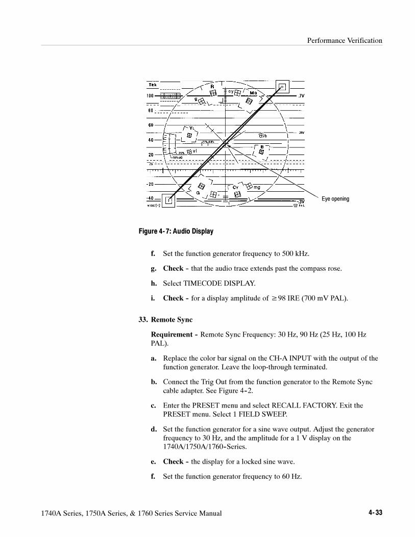
Performance Verification
1740A Series, 1750A Series, & 1760 Series Service Manual 4- 33
Eye opening
Figure 4- 7: Audio Display
f. Set the function generator frequency to 500 kHz.
g. Check -- that the audio trace extends past the compass rose.
h. Select TIMECODE DISPLAY.
i. Check -- for a display amplitude of≥98 IRE (700 mV PAL).
33. Remote Sync
Requirement -- Remote Sync Frequency: 30 Hz, 90 Hz (25 Hz, 100 HzPAL).
a. Replace the color bar signal on the CH-A INPUT with the output of thefunction generator. Leave the loop-through terminated.
b. Connect the Trig Out from the function generator to the Remote Synccable adapter. See Figure 4--2.
c. Enter the PRESET menu and select RECALL FACTORY. Exit thePRESET menu. Select 1 FIELD SWEEP.
d. Set the function generator for a sine wave output. Adjust the generatorfrequency to 30 Hz, and the amplitude for a 1 V display on the1740A/1750A/1760--Series.
e. Check -- the display for a locked sine wave.
f. Set the function generator frequency to 60 Hz.

Performance Verification
4- 34 1740A Series, 1750A Series, & 1760 Series Service Manual
g. Check -- the display for a locked sine wave.
h. Set the function generator frequency to 90 Hz.
i. Check -- the display for a locked sine wave.
j. Remove the function generator output and the Remote Cable Adapterfrom the 1740A/1750A/1760--Series.
This completes the 1740A--Series Performance Verification procedure.
34. SCH Phase Mode (1750A--Series, 1760--Series Option SC Only)
Requirement -- Absolute Accuracy: ≤5°. Color Frame Range: 70°.
a. Connect the color bar signal from the TSG-170A to the CH-A INPUT.Terminate the loop-through in 75 Ω.
b. Connect the TSG-170A Black Out to the EXT REF INPUT andterminate the loop-through in 75 Ω.
c. Select SCH DISPLAY.
d. Center the burst dot using the VERT and HORIZ POS controls. Positionthe burst vector to 0° using the VECTOR PHASE control (bezel knob).
e. Select EXT REF (front panel) and then reposition the burst vector to 0°using the VECTOR PHASE control.
f. Check -- that the SCH dots are on the compass rose.
g. Check -- that the SCH dots are within ≤5° of the 0° SCH line wheneither EXT or INT REF are selected . Note: Leave INT REF selected.
h. Enter the LINE SELECT menu and select Line 11 (Line 7 PAL) usingthe LINE SELECT control (bezel knob).
i. Connect a 75 Ω cable from the PIX OUT connector to CH1 of the testoscilloscope, terminating the oscilloscope end of the cable in 75 Ω.
j. Connect a frame black signal to CH2 of the test oscilloscope, terminat-ing the oscilloscope end of the cable in 75 Ω.
k. Set the test oscilloscope controls as follows: CH1 Volts/Div to 500 mV,DC Coupling, CH2 Volts/Div to 5 V, Chop Display Mode, DC Cou-pling, Trigger Source to CH2, Negative Trigger, and Time/Div to 2 ms.
l. Check -- that a positive-going pulse in the test oscilloscope CH1 (PIXOUT) display occurs at the same time as the pulse in the CH2 display(frame black signal).

Performance Verification
1740A Series, 1750A Series, & 1760 Series Service Manual 4- 35
m. Remove the TSG-170A signals and terminators from the CH-A and EXTREF INPUTs.
n. Connect the 1410 Black Burst signal to the CH-A INPUT. Connect a75 Ω cable from the CH-A INPUT loop-through to the EXT REFINPUT. Terminate the EXT REF INPUT in 75 Ω.
o. Exit the LINE SELECT menu and select EXT REF (front panel).
p. Adjust the television signal generator Subcarrier Phase control to placeon SCH dot on the 0° SCH line.
q. Check -- while adjusting the television signal generator Subcarrier Phasecontrol, that the display flip occurs after the SCH dot has moved 70°from the 0° SCH line.
r. Disconnect all cables and terminators from the 1750A/1760--Series.
This completes the 1750A--Series Performance Verification procedure.
35. Component Vector Gain (1760--Series Only)
Requirement -- Vertical and Horizontal Gain Accuracy: 2.5%.
a. Connect the component signals Y, B--Y, and R--Y to the CH-A1, CH-A2,and CH-A3 INPUTs respectively. Terminate the loop-throughs in 75 Ω.Set the component signal generator for SMPTE 100% color bars.
b. Select VECTOR DISPLAY and A123.
c. Enter the CONFIG menu. Select VECTOR and then select BARS 100%.
d. In the Config menu, select FORMAT, then select LIGHTNINGDISPLAY, and then select SMPTE/EBU.
e. Check -- that the component vector dots are in the graticule boxes2.5%.
f. Check -- that the component vector gain does not change whileswitching the component signal generator and the 1760--Series between100% and 75% Bars.
g. When this step is completed, leave the generator and instrument in 100%Bars.
36. Lightning Gain (1760--Series Only)
Requirement -- Vertical Gain Accuracy: 2%.
a. Select LIGHTNING DISPLAY.

Performance Verification
4- 36 1740A Series, 1750A Series, & 1760 Series Service Manual
b. Check -- that the lightning display dots are in the electronic graticuleboxes 2%.
37. Option Blanking Pulse (1760--Series Only)
Requirement -- The falling edge of the option blanking pulse occurs 0.5 s(1 s PAL) before the 50% point of the falling edge of the sync pulse0.25 s.
a. Connect the G OUTPUT to the CH2 oscilloscope input with a 75 Ω
feed-through terminator.
b. Connect a X10 probe from the CH1 oscilloscope input to A7U602 pin 9.
c. Set the oscilloscope for 10 s/Div and position the sync pulse (CH2) tothe CRT graticule center.
d. Select X10 Mag on the oscilloscope.
e. Check -- that the falling edge of the option blanking pulse (CH1) occurs0.5 s (1 s PAL) before the 50% point of the falling edge of the syncpulse (CH2)2.5 s. See Figure 4--8.
2V
100mV
1uS
50% Point
Figure 4- 8: Option Blanking Pulse
38. Bowtie Gain and Offset (1760--Series Only)
Requirement -- Bowtie gain matches CH-A1 INPUT gain 2%. BowtieDC offset between channels <5 mV.

Performance Verification
1740A Series, 1750A Series, & 1760 Series Service Manual 4- 37
a. Enter the PRESET menu and select FACTORY RECALL. Select A123.
b. Note the amplitude of the CH-A1 INPUT display.
c. Disconnect the CH-A2 INPUT signal and select BOWTIE DISPLAY.
d. Check -- that the amplitude of the Bowtie display matches the amplitudenoted in step a. 2% (2.8 IRE or 20 mV PAL).
e. Reconnect the CH-A2 INPUT signal.
f. Enter the GAIN menu and select X10.
g. Check -- that the offset between the two lines is less than 0.5 majordivisions.
h. Connect the component signals Y, B--Y, and R--Y to the CH-B1, CH-B2,and CH-B3 INPUTs respectively. Terminate the loop-throughs in 75 Ω.Leave the signal generator set for 100% SMPTE Color Bars.
i. Select B123.
j. Check -- that the offset between the two lines is less than 5 mV ( 0.75major division or 0.5 major division PAL).
39. Bowtie Common Mode Rejection Ratio (1760--Series Only)
Requirement -- ≥34 dB at 3 MHz.
a. Select the multiburst signal on the component signal generator.
b. Disconnect the signals and terminators from the CH-B1, CH-B2, andCH-B3 INPUTs.
c. Connect the component signal Y to the CH-A1 and CH-A2 INPUTs viaa 75 Ω terminator and T connector.
d. Select A123. Enter the GAIN menu and select X5.
e. Check -- that the amplitude of the 3 MHz packet is < 0.4 division. SeeFigure 4--9.

Performance Verification
4- 38 1740A Series, 1750A Series, & 1760 Series Service Manual
10S/DIV625/50
3 MHz packet
Figure 4- 9: Bowtie Common Mode Rejection Ratio
f. Disconnect the T connector and terminator from the CH-A1 and CH-A2INPUTs.
g. Connect the component signals Y, B-Y, and R--Y to the CH-A1, CH-A2,and CH-A3 INPUTs respectively. Terminate the loop-throughs in 75 Ω.
h. Select Bowtie on the component signal generator.
i. From the GAIN menu select X1.
j. Check -- for a marker in the center of the null between each channeldisplay.
40. Component Vector Registration and Phase (1760--Series Only)
Requirement -- Vector Registration -- X5 Gain: within 0.25 inches of CRTgraticule center. X10 Gain: within 0.5 inch of CRT graticule center. VectorPhase -- Less than a trace-width eye opening.
a. Select the 100% SMPTE color bars signal from the component signalgenerator.
b. Select VECTOR DISPLAY and center the display with the VERT andHORIZ POS controls.
c. Enter the GAIN menu and select X5.
d. Check -- that the signal center dot is within 1/4 inch of the CRT graticulecenter.

Performance Verification
1740A Series, 1750A Series, & 1760 Series Service Manual 4- 39
e. Select X10 from the GAIN menu.
f. Check -- that the signal center dot is within 1/2 inch of the CRT graticulecenter.
g. Select the multiburst signal on the component signal generator.
h. Select X1 from the GAIN menu.
i. Check -- for a straight line with less than a trace-width eye opening.
41. Diamond Display Phase (1760--Series Only)
Requirement -- Opening of <2 minor divisions on the vertical transition.
a. Select the 100% GBR color bars signal on the component signalgenerator.
b. Select LIGHTNING DISPLAY and MAG SWEEP on.
c. Enter the CONFIG menu. Select FORMAT, then select DISPLAYDIAMOND and GBR.
d. In the CONFIG menu select VECTOR, then select 100% BARS.
e. Check -- for an opening of < 2 minor divisions on the vertical transition.
42. GBR Picture Monitor Outputs (1760--Series Only)
Requirement -- Accuracy: 3%.
a. Connect the G OUTPUT to the test oscilloscope using a 75 Ω feed-through terminator. Set the oscilloscope for 0.1 V/Div and 10 s/Div.
b. Enter the PRESET menu and select FACTORY RECALL. SelectLIGHTNING DISPLAY and A123.
c. Enter the CONFIG menu and select VECTOR, then select 100% BARS.
d. In the CONFIG menu select FORMAT, then select DISPLAY LIGHT-NING and SMPTE/EBU.
e. Check -- for signal amplitude on the oscilloscope of 7.0 divisions 3%(0.75 division) from the baseline to the top of the 100% white bar.
f. Repeat step e. for the FORMAT menu selections of BETA, GBR, andMII.
g. Repeat steps d. through f. for the B and R OUTPUTs.
This completes the 1760--Series Performance Verification procedure.

Performance Verification
4- 40 1740A Series, 1750A Series, & 1760 Series Service Manual

1740A Series, 1750A Series, & 1760 Series Service Manual 5- 1
Adjustments
The adjustment procedures for the 1740A/1750A/1760 Series are loaded on the3 1/2 inch high-density disk included in this manual (Tektronix part number063-1690-XX).
This section lists recommended equipment, shows initial setups and providesboard locations for adjustments. The instrument software version must be 2.2 orgreater to use this Adjustment Procedure.
To determine the software version loaded in the instrument, check the lower rightcorner of the REMOTE submenu of the front panel selected CONFIG menu. Ifthe software version is lower than 2.2, load new operating software from thesoftware disk included with this manual. See Installation for instructions.
Required Equipment
The following equipment and accessory items are required to perform theadjustment procedures. Broad specifications are followed by an example ofspecific equipment that meet these specifications.
1. IBM Compatible PC
System requirements:DOS 3.3 or higher.640K bytes of random-access memory (RAM).High-density floppy drive (3.5 inch/144 MB).Available RS232 Port (COM 1, 2, 3, or 4).
2. Test Oscilloscope
Vertical Amplifier:30 MHz Bandwidth, 2 mV Sensitivity.
Time Base:10 ns/div to 5 ms/div sweep speeds, Triggering to 50 MHz.
For example:A TEKTRONIX TAS 465 Oscilloscope. Also 10X probe, P6109B, and 1Xprobe, P6119B.
Electrical Instruments

Adjustments
5- 2 1740A Series, 1750A Series, & 1760 Series Service Manual
3. Television Signal Generator
Color test signals for the television standard of the monitor to be tested:Color bar signal, multiburst signal, and black burst signal.
For example:NTSC Tektronix 1410 with Option AA and Option AB (modified SPG2 andTSG7), TSG3, and TSG5.
PAL Tektronix 1411 with Option AA and Option AB (modified SPG12 andTSG17), TSG13, and TSG15.
NOTE. 1410--Series Generators:
The 1410--Series generators with standard SPG and TSG modules can be used,
but not all checks and adjustments can be made. The standard SPG2/SPG12
modules will not check lock to changes in sync amplitude, cw lock to changes in
burst amplitude, or frequency lock to burst offset frequency changes.
The signal generator can be ordered with one or both options (AA and AB).
4. Digital Television Signal Generator
For example:Tektronix TSG-170A NTSCTektronix TSG-271 PALTektronix TSG-300 Component
5. Swept Sine Wave Generator
Frequencies from 50 kHz to 10 MHz. CW signal can be used as time marks.
For example:HP3336C, Option 005. Option 005 provides increased flatness and attenua-tor accuracy (+0.07 dB flatness in CW mode). The standard frequencyaccuracy (+5 ppm of programmed frequency) is sufficient for time baseverification.
6. Square Wave Generator
Range: 0.1 to 5 Vp-p when loaded by 75 Ω; 10 Vp-p when unloaded.Frequency: 10 Hz to 2 kHz.
For example:Tektronix FG503 installed in a TM500--Series Power Module.

Adjustments
1740A Series, 1750A Series, & 1760 Series Service Manual 5- 3
7. Variable Autotransformer
For example:General Radio Metered Auto Transformer W10MT3W. If 220 V operationmust be checked, a conversion transformer or appropriate 220 V autotrans-former is needed.
8. Voltmeter
Range: 0 to >100 Vdc. Accuracy: 0.1%.
For example:Tektronix DM501A installed in a TM500--Series Power Module.
9. Video Amplitude Calibrator (VAC)
Signal: Adjustable square wave 0.0 to 999.9 mVp-p. Resolution: 0.1 mV.Accuracy: 0.05%. Frequency: Approximately 270 Hz.
For example:Tektronix 067-0916-00 installed in a TM500--Series Power Module.
10. Peak-to-Peak Detector
Input Signal Range: 0.25 to 1.0 Vp-p. Flatness: 0.2% 50 kHz to 10 MHz.Input Impedance: 75 Ω.
For example:Tektronix Part No. 015-0408-00 (includes Peak-to-Peak Detector Head015-0413-00) installed in a TM500--Series Power Module.
11. Power Module
For powering and housing Tektronix SG505, FG503, DM501A, DC503A,067-0916-00, and a 015-0408-00.
For example:Tektronix TM500--Series Power Module.
12. Low-Distortion Oscillator
1-kHz balanced output, 387 mV to 1.54 V amplitude.
For example:Tektronix FG501A

Adjustments
5- 4 1740A Series, 1750A Series, & 1760 Series Service Manual
13. 75 Ω Terminators
14. Six required; two end-line and four feed-through type.
For example:End-line, 75 Ω terminator (Tektronix Part No. 011-0102-00).Feed-through, 75 Ω terminator (Tektronix Part No. 011-0103-02).
15. Coaxial Cable
Three 75 Ω cables required; one 50 Ω cable required.
For example:75 Ω -- 42-inch RG59U (Tektronix Part No. 012-0159-00).50 Ω -- 42-inch RG58U (Tektronix Part No. 012-0057-01).
16. Dual-Input Coupler
Matched BNC cable-T for making phase comparisons between two inputs.Matched length of the two arms within 0.1 inch.
For example:Tektronix Part No. 067-0525-02.
17. BNC Female-to-Dual Banana Adapter
Two required.
For example:Tektronix Part No. 103-0090-00.
Auxiliary Equipment

Adjustments
1740A Series, 1750A Series, & 1760 Series Service Manual 5- 5
18. External horizontal/RGB and YRGB cable adapter
114
1325
3
25-Pin male connectorto remote connector
Connect to ground
Signal
Female BNC
Figure 5- 1: External horizontal/RGB and YRGB cable adapter
19. Remote sync cable adapter
5
14
1325
6
25-Pin male connectorto remote connector
Connect to ground
Signal
Female BNC
Figure 5- 2: Remote sync cable adapter
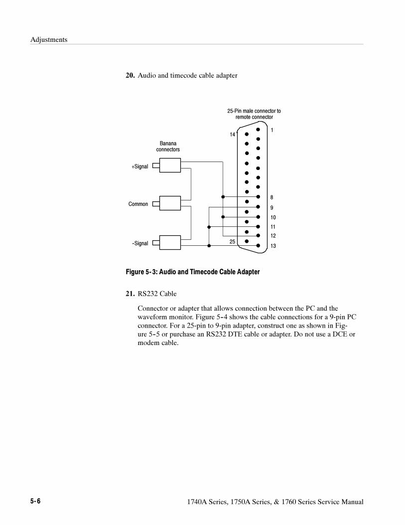
Adjustments
5- 6 1740A Series, 1750A Series, & 1760 Series Service Manual
20. Audio and timecode cable adapter
114
1325
25-Pin male connector toremote connector
--Signal
Bananaconnectors
8
9
10
11
12
Common
+Signal
Figure 5- 3: Audio and Timecode Cable Adapter
21. RS232 Cable
Connector or adapter that allows connection between the PC and thewaveform monitor. Figure 5--4 shows the cable connections for a 9-pin PCconnector. For a 25-pin to 9-pin adapter, construct one as shown in Fig-ure 5--5 or purchase an RS232 DTE cable or adapter. Do not use a DCE ormodem cable.
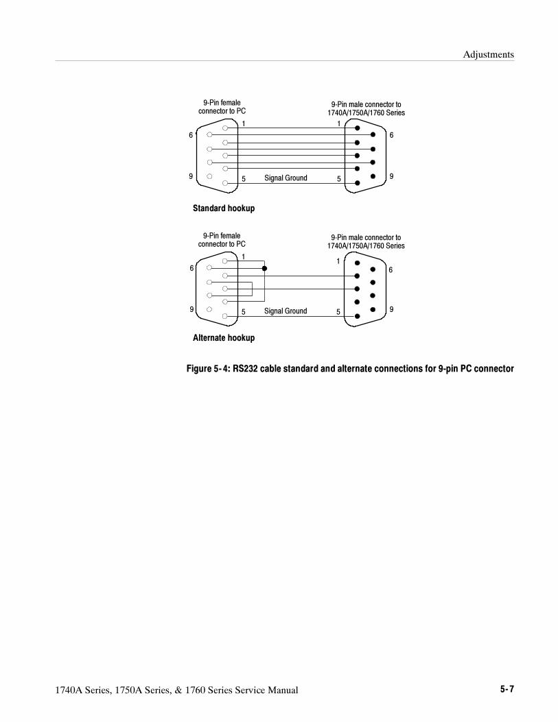
Adjustments
1740A Series, 1750A Series, & 1760 Series Service Manual 5- 7
1
6
9 5 Signal Ground
9-Pin femaleconnector to PC
9-Pin male connector to1740A/1750A/1760 Series
1
6
95
Standard hookup
16
5
1
6
9 5 Signal Ground
9-Pin femaleconnector to PC
9-Pin male connector to1740A/1750A/1760 Series
9
Alternate hookup
Figure 5- 4: RS232 cable standard and alternate connections for 9-pin PC connector

Adjustments
5- 8 1740A Series, 1750A Series, & 1760 Series Service Manual
114
1325
2
3
4
5
16
95
7
9-Pin male connector to1740A/1750A/1760 Series
25-Pin femaleconnector to PC
2
3
820
Signal ground
6
114
1325
2
3
4
5
1
6
95
7
9-Pin male connector to1740A/1750A/1760 Series
25-Pin femaleconnector to PC
2
3
8
20
Signal ground
6
Standard hookup
4
7
8
Alternate hookup
Figure 5- 5: RS232 cable standard and alternate hookups for 25-pin PC connector
22. Magnifying Glass
May be useful for viewing the CRT graticule.
Optional Equipment

Adjustments
1740A Series, 1750A Series, & 1760 Series Service Manual 5- 9
Initial Setup
1. Initial Equipment Setup
a. Connect an RS232 cable from the 1740A/1750A/1760 Series rear-panelRS232 connector to the COM 1, 2, 3, or 4 connector on the PC. See theRequired Equipment List for the cable wiring illustrations.
NOTE. Cable Wiring: If the RXD and TXD pins are swapped, as in some modem
connections, the Adjustment Procedures program will not operate.
b. Connect the power source to the 1740A/1750A/1760 Series and turn onthe instrument.
NOTE. Instrument Power: The 1740A/1750A/1760 Series power switch must be
set to ON before the Adjustment Procedures program is started. If the instrument
is not turned on, the PC will not be able to establish communications with the
instrument. Turning the instrument power ON after the Adjustment Procedures
program is started can cause the PC to lock up, requiring a system reset.
c. Enter the Configure menu on the 1740A/1750A/1760 Series. From themenu, select REMOTE and then BAUD 9600. Exit the Configure menu.
NOTE. The 1740A/1750A/1760 Series RS232 interface baud rate must be set to
9600 baud. If the baud rate is set to 1200 or 4800 baud, the PC will not be able
to establish communications with the instrument.
2. Load the Adjustment Procedures program:
a. This manual section was written for the Adjustment Procedures programversion 1.0. Verify that the Adjustment Procedures disk is version 1.0.
b. Insert the Adjustment Procedures disk into the PC disk drive.
c. At the PC DOS prompt, type the drive letter for the floppy drive to beused, followed by a colon, and then press the Return key.For Example, A: <RETURN>
NOTE. The Adjustment Procedures program will run faster if loaded on the PC
hard drive. To load the program on the PC hard drive, create a directory on the
PC hard drive and copy the contents of the disk into the directory.
d. Type CAL and then press the Return key. The program will prompt for afew parameters before the adjustment steps start.

Adjustments
5- 10 1740A Series, 1750A Series, & 1760 Series Service Manual
Functional Description of PC Display
Figure 5--6 shows a sample adjustment screen on the PC. The numbers aboveand below the illustration match with descriptions on the following page.
Tek 1760 FULL ADJUSTMENT
WFM INTENSITY
STEP 6 of 64
F8 F9 F10 change Adj. Size
STEP 6. WAVEFORM DISPLAY INTENSITY
F1--HELP F2--SETUP F3--NEXT F4--BACK F5--RESTART F6--STEP F7--EXIT
a. ADJUST -- WFM INTENSITY for normal display intensity.
b. Select VECTOR DISPLAY (Front Panel).
C. ADJUST -- VECTOR INTENSITY for normal display intensity.
d. Select AUDIO DISPLAY (Front Panel).
e. ADJUST -- AUDIO INTENSITY for normal display intensity.
f. Select WAVEFORM DISPLAY (Front Panel).
g. Enter the LIN SEL MENU and select 1H (CRT menu).
<PAGE DOWN FOR MORE INSTRUCTIONS>
to adjustVECTOR INTENSITY
AUDIO INTENSITY
JOB.NAME
to adjust
Adj. SizeX10
PREVIEW MODE
3 214 56
7 8 9 1011 12
Figure 5- 6: Typical adjustment procedures PC screen display

Adjustments
1740A Series, 1750A Series, & 1760 Series Service Manual 5- 11
1 Instrument type and procedure being performed.
2 Current step number and how many steps are in the procedure being performed.
3 Name of the job. Appears when the procedure being performed is a saved job.
4 Function keys that are active during the program. They function as follows:
F1 Opens the Help Menu.
F2 Opens the Setup Window, showing the initial equipment connections for thecurrent step. These are the only connections that should be in place whenthe step is started; remove all other connections from previous steps.
F3 Goes to the next step in the adjustment procedure.
F4 Goes to the previous step in the adjustment procedure.
F5 Goes to the beginning of the current step; front-panel / internal instrumentsettings return to the state they were in when the current step was started.
F6 Opens the Select Step window, where you can select any step in theprocedure to perform. To select a step, press PAGE UP or PAGE DOWN.To close the window and return to the current step, press ESC.
F7 Opens the Exit Menu, where you can change procedure types, save thecurrent Adjustment job, or exit to DOS.
5 Indicates that the procedure is in the Preview Mode.
6 Displays the current step number and title.
7/8 Indicates which arrow keys control the adjustment. (Appears when the currentstep has adjustments controlled by the arrow keys.)
9 Function keys set the adjustment amount of the Up /Down arrow keys. (Appearswhen the current step has an adjustment controlled by the Up/Down arrow keys.)
F8 Selects X1; use to fine tune an adjustment to exact position.
F9 Selects X10; (default) use to bring an adjustment close to proper position.
F10 Selects X100; use for roughing in adjustments that are far out of position.
10 Displays the current arrow key adjustment size.
11 Lists adjustments for the current step. The active adjustment is highlighted. TheLeft/Right PC arrow keys control the adjustment selection.
12 Displays the procedure steps to be performed. If additional steps are indicated,press PAGE DOWN.

Adjustments
5- 12 1740A Series, 1750A Series, & 1760 Series Service Manual
Circuit Board Adjustment Locations
Figures 5--7 through 5--11 show the adjustment locations on the circuit boards.
R9
J1R42
J2
R38 R44 R53
R73
J4
TP1
GND
W2
W1
W3
R69
Mains voltage
Figure 5- 7: A1 Power Supply board
J1
J2 J5
J6
C73
R168
BRN
U53
R134
R135
J9U78
J12
J13
J14
R182
R183C91
C131
L6L5
C151 C154
C135 C137
RED
Figure 5- 8: A3 Main board

Adjustments
1740A Series, 1750A Series, & 1760 Series Service Manual 5- 13
R36
C26
L2
P1
J1
C106
C109
TP1
Figure 5- 9: A5 Vector board
J1
TP3
TP4
R173
C46
TP1
C42
TP2
C64
C69
Figure 5- 10: A6 SCH board

Adjustments
5- 14 1740A Series, 1750A Series, & 1760 Series Service Manual
J9
C136 C135U126
C111
U161
C74
R601
J12 J13
R122
R159
Figure 5- 11: A7 Component board

Adjustments
1740A Series, 1750A Series, & 1760 Series Service Manual 5- 15
Waveform Illustrations
The following waveform illustrations are provided as a reference. The illustra-tions are of the 1765 unless otherwise noted.
10S/DIVNTSC
Thinnesttrace
Figure 5- 12: Adjusting for thinnest luminance step
10S/DIVNTSC
Match transient responses
Figure 5- 13: Matching flat and luminance filter responses

Adjustments
5- 16 1740A Series, 1750A Series, & 1760 Series Service Manual
2V
2V
50uS
Figure 5- 14: Adjusting the NTSC SCH on the oscilloscope
NTSC
Approximateflipping points
Figure 5- 15: Matching the SCH dot flipping points

Adjustments
1740A Series, 1750A Series, & 1760 Series Service Manual 5- 17
2V
100mV
1uS
50% Point
Figure 5- 16: Adjusting the option blanking pulse
10S/DIV625/50
3 MHz packet
Figure 5- 17: Adjusting for minimum Bowtie amplitude

Adjustments
5- 18 1740A Series, 1750A Series, & 1760 Series Service Manual
625/50
Adjust forminimum opening
Figure 5- 18: Adjusting Diamond display phase

1740A Series, 1750A Series, & 1760 Series Service Manual 6- 1
Maintenance
This section contains instructions for preventive maintenance, general trouble-shooting, and corrective maintenance. If the instrument does not functionproperly, troubleshooting and corrective measures should be taken immediatelyto circumvent additional problems.
Preventing ESD
CAUTION. Static discharge can damage any semiconductor component in this
instrument.
When performing any service which requires internal access to the instrument,adhere to the following precautions to avoid damaging internal modules and theircomponents due to electrostatic discharge (ESD).
1. Minimize handling of static-sensitive circuit boards and components.
2. Transport and store static-sensitive modules in their static protected contain-ers or on a metal rail. Label packages containing static-sensitive boards.
3. Discharge the static voltage from your body by wearing a grounded antistaticwrist strap while handling these modules. Do service of static-sensitivemodules only at a static-free work station.
4. Nothing capable of generating or holding a static charge should be allowedon the work station surface.
5. Handle circuit boards by the edges when possible.
6. Do not slide the circuit boards over any surface.
7. Avoid handling circuit boards in areas that have a floor or work-surfacecovering capable of generating a static charge.
Preventive Maintenance
Preventive maintenance consists of inspection and cleaning, performance checks,and, if needed, readjustment. The preventive maintenance schedule establishedfor the instrument should be based on the environment in which it is operatedand the amount of use. Under average conditions, scheduled preventivemaintenance should be performed every 2000 hours of operation.

Maintenance
6- 2 1740A Series, 1750A Series, & 1760 Series Service Manual
Performance Checks and Adjustments
Instrument performance should be checked after each 2000 hours of operation, orevery 12 months. This will help to ensure maximum performance and assist inlocating defects that may not be apparent during regular operation. ThePerformance Check Procedure and the Adjustment Procedures are included inthis manual.
Inspection and Cleaning
Inspection and Cleaning describes how to inspect for dirt and damage. It alsodescribes how to clean the exterior and interior of the instrument. Inspection andcleaning are done as preventive maintenance. Preventive maintenance, whendone regularly, may prevent instrument malfunction and enhance its reliability.
Preventive maintenance consists of visually inspecting and cleaning theinstrument and using general care when operating it.
How often to do maintenance depends on the severity of the environment inwhich the instrument is used. A proper time to perform preventive maintenanceis just before instrument adjustment.
The cabinet helps keep dust out of the instrument and should normally be inplace when operating the instrument.
WARNING. Before performing any procedure that follows, power down the
instrument and disconnect it from line voltage.
Use a dry, low-velocity stream of air to clean the interior of the chassis. Use asoft-bristle, nonstatic-producing brush for cleaning around components. If youmust use a liquid for minor interior cleaning, use a 75% isopropyl alcoholsolution and rinse with deionized water.
CAUTION. Avoid the use of chemical cleaning agents which might damage the
plastics used in this instrument. Use only deionized water when cleaning the
menu buttons or front-panel buttons. Use a 75% isopropyl alcohol solution as a
cleaner and rinse with deionized water. Before using any other type of cleaner,
consult your Tektronix Service Center or representative.
General Care
Interior Cleaning

Maintenance
1740A Series, 1750A Series, & 1760 Series Service Manual 6- 3
Clean the exterior surfaces of the chassis with a dry lint-free cloth or a soft-bristle brush. If any dirt remains, use a cloth or swab dipped in a 75% isopropylalcohol solution. Use a swab to clean narrow spaces around controls andconnectors. Do not use abrasive compounds on any part of the chassis that maydamage the chassis.
Clean the On/Standby switch using a dampened cleaning towel. Do not spray orwet the switch directly.
Inspect the outside of the instrument for damage, wear, and missing parts, usingTable 6--1 as a guide. Immediately repair defects that could cause personal injuryor lead to further damage to the instrument.
Table 6- 1: External inspection check list
Item Inspect for Repair action
Cabinet, front panel, cover Cracks, scratches, deformations, damaged hardware Repair or replace defective module.
Front-panel knobs Missing, damaged, or loose knobs Repair or replace missing or defective knobs.
Connectors Broken shells, cracked insulation, and deformedcontacts. Dirt in connectors.
Repair or replace defective modules. Clear orwash out dirt.
Carrying handle, cabinet feet Correct operation Repair or replace defective module.
Accessories Missing items or parts of items, bent pins, broken orfrayed cables, damaged connectors
Repair or replace damaged or missing items,frayed cables, and defective modules.
Clean the CRT protective shield, light filter, and CRT face with a soft, lint-freecloth dampened in denatured alcohol.
The instrument requires a clean, unrestricted internal air flow. The air filter islocated on the rear panel and should be checked frequently for dust and grimebuildup. A supply of replacement filters was shipped with this instrument.
The air filters supplied with this instrument can be washed in warm water anddetergent and reused. To replace a filter, remove two screws from the fan cover,lift out the old filter and replace it. Install the cover with the two mountingscrews. Do not overtighten the screws.
You can order additional air filters directly from Tektronix. The part number forthe air filters is listed with the Optional Accessories at the rear of the MechanicalReplaceable Parts list, at the back of this manual.
An instrument may contain older software and therefore not perform up to theexpected level. Before servicing, enter the REMOTE submenu from the main
Exterior Cleaning
Cleaning the CRT
Maintaining the Air Filter
Software Version

Maintenance
6- 4 1740A Series, 1750A Series, & 1760 Series Service Manual
CONFIG menu and verify the software version number in the lower right cornerof the screen. To update the operating software, go to page 2--14.
1. Ensure that the malfunction exists in the instrument. Ensure that theinstrument is operating as intended by Tektronix (see Operating Instruc-tions), and check that a malfunction has not occurred up stream from thewaveform monitor.
2. Determine and evaluate all trouble symptoms. Isolate the problem to ageneral area such as an assembly. Use the block diagram to help in signaltracing and circuit isolation.
CAUTION. Use extreme care when probing with meter leads or probes, becauseof the high component density and limited access within the instrument. Theinadvertent movement of leads or a probe could cause a short circuit ortransient voltages capable of destroying components.
3. Determine the nature of the problem. Determine whether the instrument isout of calibration or if there has been a component failure. Then identify thefunctional area most likely at fault.
4. Inspect the suspect assembly for defects. Look for broken or loose compo-nents, improperly seated components, overheated or burned components,chafed insulation, etc. Repair or replace all obvious defects. Determine and
correct the cause of any overheating before reapplying power.
5. Use successive electrical checks to locate the source of the problem. Use thePerformance Check Procedure to determine if a circuit is operating withinspecifications. It may be necessary to change a calibration adjustment todetermine if a circuit is operational, but since this can destroy instrumentcalibration, care should be exercised. Before changing an adjustment, note itsposition so that it can be returned to its original setting.
6. Determine the extent of the repair. If the necessary repair is complex, it maybe advisable to contact Tektronix before continuing. If the repair is minor,such as replacing a component, see the parts list for replacement information.
CAUTION. Always remove the assembly from the instrument before replacing asoldered-in component. See Corrective Maintenance for the correct procedure.
General TroubleshootingTechniques

Maintenance
1740A Series, 1750A Series, & 1760 Series Service Manual 6- 5
Replacing the Line Fuse
This instrument is protected with an F-type cartridge fuse, located in a holder,directly above the line cord receptacle on the rear panel. The fuse should only bereplaced with the correct type and value. Using a higher rated or slo blo fusecould cause circuit damage. The correct value and type is silk screened on therear panel, adjacent to the fuse holder.
Troubleshooting
WARNING. Read Instructions! To avoid personal injury or damage to equipment,
do not attempt to troubleshoot this Power Supply without reading the following
instructions.
The Power Supply is a switching type and requires a specific troubleshootingprocedure to avoid personal danger or instrument damage. The followingTroubleshooting procedure will help to isolate a problem to a specific circuit.Then you can analyze the circuit or use part substitution to find the defectivecomponent(s).
The equipment needed to troubleshoot the power supply:
Digital Multimeter (DMM), with a diode check function
Oscilloscope
20 VDC Variable Power Supply
5 VDC Power Supply
High Voltage Probe, ≥1 G Ω input resistance
NOTE. You should read the power supply Theory of Operation before repairing
the power supply.
The Troubleshooting Procedure for the Power Supply (Assembly A1) is split intotwo sections: the Low Volts and High Volts Supplies. Start the procedure bydetermining which section of the Power Supply the problem is in. With thePower Supply installed in the instrument, apply AC power and turn on thefront-panel POWER switch. From Table 6--2, determine which symptom thePower Supply exhibits and refer to the corresponding procedure.
Power Supply
TroubleshootingProcedure
Introduction

Maintenance
6- 6 1740A Series, 1750A Series, & 1760 Series Service Manual
Table 6- 2: Power supply fault symptoms
Symptom Procedure
Line fuse open Rectifier/Switcher/Snubber Check
Power Supply cycles OFF/ONNote: Check instrument for shorts.
Output CheckError Amplifier CheckShutdown Logic Check
Does not power up Controller/Gate Drive CheckTransformer Driver CheckError Amplifier CheckShutdown Logic CheckRectifier/Switcher/Snubber Check
+5 V not regulating Error Amplifier Check
Improper CRT display High Volts Supply Checks
1. Preliminary Checks
a. A properly functioning and loaded Low Volts Supply will output thevoltages listed in Table 6--3. Use the DMM to measure the voltagesbetween TP1 and the voltage test points. If the supply is not regulatingproperly, continue with the procedure.
Table 6- 3: Low volts supply voltages
Test Point Voltage Range
W1 -- (+5 V) +5.0 V
W4 -- (+11 V) +10.5 to +12.0 V
W3 -- (--11 V) --10.5 to --12.0 V
W2 -- (+40 V) +39.0 to +41.0 V
NOTE. Troubleshoot the Low Volts power supply without applying AC power.
b. Disconnect AC power from the instrument. Disconnect the instrumentfrom the Power Supply by removing the plug jumper from J4.
c. Use the digital multimeter to measure the voltage between TP2 and thetab (drain) of Q14. Check that the voltage is near 0 V.
Low Volts Supply

Maintenance
1740A Series, 1750A Series, & 1760 Series Service Manual 6- 7
WARNING. To prevent personal injury or damage to equipment, do not proceed
until the drain of Q14 is near 0 V. Dangerous voltage potentials are present in
the circuit until the capacitors discharge.
2. Rectifier/Switcher/Snubber Check
a. Use the digital multimeter to measure the voltage between TP2 and TP3.Be sure the voltage is near 0 V before proceeding.
b. Remove the plug jumper P7.
c. With the negative lead of the digital multimeter connected to TP3 andthe positive lead connected to TP2, measure the circuit resistance. Aresistance of less than 20 kΩ indicates a shorted mosfet (Q14). If themosfet is shorted, replace it and perform the Control Circuit Check.
d. Using the digital multimeter diode test function, test CR32, CR33,CR34, and CR35 for shorts. Diode replacements must be fast reverserecovery (300 ns) types to reduce conducted noise.
e. Using the digital multimeter diode test function, test the snubber diodesCR23 and CR25 for shorts.
f. Replace P7.
3. Output Check
a. Connect the negative output from the 20 VAC Power Supply to TP1 andits positive output to W3 (+11 V). The circuit should draw less than20 mA. Excessive current draw can be caused by CR16 or U2 (HighVolts power supply).
NOTE. The variable power supply used in the following checks must have a
current limit of 1 ampere or less.
b. Connect the negative output from the 20 VAC Power Supply to TP1 andthe positive output to R69 (+40 V). The circuit should draw less than20 mA. Excessive current draw can be caused by CR19 or Q7 (HighVolts Power Supply).
c. Connect the positive output from the 20 Power Supply to TP1and thenegative output to W2 (--11 V). The circuit should draw less than 20 mA.Excessive current draw can be caused by CR18.
d. Connect the negative output from the 5 Power Supply to TP1 and thepositive output to W1 (+5 V). The circuit should draw less than 20 mA.Excessive current draw can be caused by CR17 or Q1 and Q2 (HighVolts Power Supply).

Maintenance
6- 8 1740A Series, 1750A Series, & 1760 Series Service Manual
4. Controller/Gate Drive Check
a. Connect the negative 20 VDC Power Supply output to TP3. Connect thepositive output to the cathode of CR22. Short the emitter and base ofQ15 together. Connect the oscilloscope probe ground to TP3. When thecontrol circuit functions properly, the signals in Table 6--4 are present.
b. Use the oscilloscope to observe the signal at the cathode of CR28. Itshould be an 80 kHz square wave, switching between --1 and 12 volts.The fall time is 0.2 s and the rise time is 1 s.
c. Remove the short from across Q15.
Table 6- 4: Control Circuit Test Points
Circuit Location Signal
U6, pin 1 Approximately 5 VDC
U6, pin 2 Approximately 1 to 2 VDC
U6, pin 3 0 V
U6, pin 4 80 kHz triangle wave, 2 V p-p
U6, pin 6 80 kHz square wave, 18 V p-p
5. Transformer Driver Check
a. Connect the negative output from the 20 VDC Power Supply to TP3.Connect the positive output to the cathode of CR22.
b. Connect the negative output from the 5 VDC Power Supply to TP3.Connect the positive output to the cathode of VR3.
c. Connect the oscilloscope probe ground to TP3.
d. Using the oscilloscope, observe the signal at U8, pin 5. It should togglebetween 0 and 5 VDC when J3 is shorted and unshorted. If the pulse isnot present, continue with the check.
e. Using the oscilloscope, observe the signal at U8, pin 3. A positive-go-ing, 100 ms pulse should occur when J3 is shorted and unshorted.
If the pulse is not present, use the oscilloscope to observe the signal atU5, pin 1. It should be a logical high when J3 is unshorted and a logicallow when it is shorted.
If the signal is not present, use the oscilloscope to observe the signal atthe collector of Q13. With J3 unshorted, this point should have a 1 V,170 kHz sine wave riding on 5 VDC. With J3 shorted this point shouldbe at 5 VDC.

Maintenance
1740A Series, 1750A Series, & 1760 Series Service Manual 6- 9
6. Error Amplifier/Voltage Reference/Over Voltage Check
a. Set the variable Power Supply to 4.6 VDC. Connect the negative lead toTP1 and the positive output to W1 (+5 V).
b. Connect the digital multimeter common lead to TP1.
c. Using the digital multimeter, measure the voltage at U3, pin 6. It shouldbe 0 V.
d. Using the digital multimeter measure the voltage at U3, pin 1. It shouldbe 2.5 V.
e. Set the variable Power Supply to 5.4 V.
f. Using the digital multimeter measure the voltage at U3, pin 6. It shouldbe 5 V.
g. Slowly increase the voltage of the variable Power Supply. Before 6 V isreached, the over voltage protection circuit should fire and pull thevoltage below 1 V.
7. Shut Down Logic Check
a. Connect the negative output of the 20 VDC Power Supply to TP3.Connect the positive output to the cathode of CR22.
b. Connect the digital multimeter common lead to TP3.
c. Measure the voltages according to Table 6--5 to see if the shut downlogic circuit is functioning properly.
Table 6- 5: Shut down logic levels
Circuit Location Approximate Voltage
U7, pin 1 0 V
U7, pin 4 2 VDC
U7, pin 6 3 VDC
U7, pin 7 4.15 VDC
U7, pin 9 0.3 VDC
d. Using the digital multimeter, measure the voltage at U6, pin 3. It shouldbe approximately 5 VDC. Short the base to the emitter of Q15. Pin 3should now measure 0 V.

Maintenance
6- 10 1740A Series, 1750A Series, & 1760 Series Service Manual
WARNING. Dangerous potentials exist on this circuit board. To avoid personal
injury or damage to equipment, exercise extreme care when troubleshooting
these circuits.
1. Preliminary Checks
a. Table 6--6 lists the High Volts Supply fault symptoms and procedures.
Table 6- 6: High Volts Supply Fault Symptoms
Symptom Procedure
Unable to focus CRT using thefront-panel control
Focus Amplifier Check
Unable to adjust CRT intensity usingthe front-panel control
Z-Axis Amplifier CheckGrid Drive Check
No CRT display High Voltage Oscillator CheckCRT Voltage Check
b. Load the Low Volts Supply with the instrument.
2. Focus Amplifier Check
a. Using the digital multimeter, measure the voltage between TP1 and thecollector of Q2.
b. It should vary from 0 to --300 VDC when the front-panel FOCUS controlis rotated.
3. Z-Axis Amplifier Check
a. Using the digital multimeter, measure the voltage between TP1 and thecollector of Q6.
b. Short together the base and emitter of Q3. The collector of Q6 should benear 0 V.
c. Short together the base and emitter of Q4. The collector of Q6 should benear 0 V.
High Volts Supply

Maintenance
1740A Series, 1750A Series, & 1760 Series Service Manual 6- 11
4. Grid Drive Check
a. Turn off the Power Supply. Use the diode check on the digital multime-ter to test CR2, CR5, CR6, CR8, and CR9 for shorts.
b. Power up the Power Supply.
c. Using the digital multimeter, measure the voltage between TP1 and thecathode of CR8. It should vary between approximately +40 and +170 Vas R58 (CRT Bias) is adjusted.
5. High Voltage Oscillator Check
a. Connect the oscilloscope probe to T1 pin 3 (Q6 collector) and the probeground to TP1. Power up the supply. The signal should be a +70 V p-p,22 kHz sine wave.
b. Check the voltages listed in Table 6--7 using the digital multimeter:
Table 6- 7: High voltage oscillator test points
Circuit location Voltage
T1, pin 4 Approximately +40 V
T1, pin 13 Less than +2 V
U2, pin 2 Approximately +4.8 V
U2, pin 6 +4 to +11 V
CR9, cathode Approximately +100 V
6. CRT Voltage Check
NOTE. High-Voltage Probe: This check requires a high-voltage probe having an
input resistance of 1 G Ω or more.
a. Connect the high-voltage probe ground to TP1.
b. Power up the Power Supply.
c. Use the high-voltage probe to measure the voltage at the anode of CR4.It should be approximately --2530 V.
d. Measure the voltage at the anode end of CR3. It should be 50--150 Vmore negative than the reading from the anode of CR4.

Maintenance
6- 12 1740A Series, 1750A Series, & 1760 Series Service Manual
Corrective Maintenance
Tektronix maintains a service organization that can provide a number of servicesto assist in maintaining the instrument(s) operation at its specified levels. Formore information, refer to Contacting Tektronix on page xiv.
Circuit Boards
The circuit boards are designated as assemblies, which are listed at the beginningof the Replaceable Electrical Parts list in this manual. Figure 6--1 shows thelocations of all circuit board assemblies. An instrument with serial number aboveB030000 is illustrated, but the circuit board locations are also valid for instru-ments from B020000 to B029999.
A7(1760 Series Only)
A6(1750A Series &
1760 Series Opt SC Only)
A4
A5
A3
A1A2
A10(B030000 and above)
Figure 6- 1: Instrument etched circuit board assemblies

Maintenance
1740A Series, 1750A Series, & 1760 Series Service Manual 6- 13
Mechanical Disassembly/Assembly
The instructions contained here are for disassembly. Reassembly is performed byreversing the order of the steps used to disassemble the instrument.
WARNING. To avoid personal injury or damage to equipment, disconnect the
power cord before attempting any disassembly of the instrument.
CAUTION. Do not reinsert screws in the rear panel when the instrument is
removed from the cabinet.
1. Remove the five knobs located below the CRT, using a 1/16-inch Allenwrench. See Figure 6--2.
Removeknobs (5)
Removescrews (2)
Figure 6- 2: Removing the CRT bezel
Removing the Bezel

Maintenance
6- 14 1740A Series, 1750A Series, & 1760 Series Service Manual
2. Use the screwdriver tip to push out on the inside of the center of the smallpanel located immediately below the CRT. This exposes the two bezelmounting screws.
NOTE. All screws, unless otherwise noted, are TORX screws and can be removed
with a T15 screwdriver tip. The exception is #2 Pozidrive screws which can be
removed with a #1 Pozidrive tip).
3. Remove the two bezel screws.
4. Grasping the bottom of the bezel, pull straight out and upward. There aretwo hinges at the top of the bezel that hold it in place; once the bezel is at anapproximate45° angle with the front panel they will disengage.
5. To replace, reverse the procedure, pushing in on the small panel instead ofout.
For graticule light removal and replacement, tweezers with curved, serrated tipsare recommended. For example, Miltex PL312,6--100 (equivalent to PL312) orPL317 (longer than PL312).
Replacement bulbs are supplied with this instrument as Standard Accessories.Additional bulbs can be purchased from Tektronix (see Replaceable ElectricalParts list) or from local electronics distribution sources.
CAUTION. Needle-nosed pliers are not recommended for bulb replacement.
1. Procedure
2. Remove the bezel according to the preceding instructions.
3. To remove a bulb, position the tweezer tips or grasp the thin, flat portion ofthe bulb (close to the plastic socket). Carefully pull the bulb straight out. SeeFigure 6--3.
Replacing the GraticuleLight

Maintenance
1740A Series, 1750A Series, & 1760 Series Service Manual 6- 15
Install bulb
Figure 6- 3: Replacing graticule light bulbs
4. To install a bulb, hold it with the tweezers or fingers as described in steptwo, position it in front of the socket, and push the bulb with your fingeruntil it snaps into place.
5. Replace the bezel.

Maintenance
6- 16 1740A Series, 1750A Series, & 1760 Series Service Manual
To replace a CRT in an instrument with serial number below B030000, order anupgrade kit from Tektronix and follow the instructions in the kit.
To remove the CRT in an instrument with serial number B030000 or greater, usethe following procedure. Figure 6--4 illustrates the CRT removal.
WARNING. The CRT is a high vacuum device and must be handled with care. To
avoid personal injury, always wear safety glasses, gloves, and protective
clothing when handling CRTs.
1. Remove the bezel and the CRT light filter. See Removing the CRT Bezel onpage 6--13.
2. Cut the retaining clip that goes around the CRT shield.
CAUTION.When disconnecting the CRT Socket board from the CRT, be careful
not to bend the pins on the back of the CRT.
3. Carefully disconnect the CRT socket board from the back of the CRT. Pullthe board straight out so that you do not bend the CRT pins.
4. Disconnect the cable from J3 (trace rotation) on the Main board and push theconnector through the hole in the board.
WARNING. The CRT may retain a dangerous charge. To avoid personal injury or
damage to equipment, ground the anode to discharge the CRT. Do not allow the
conductor to touch your body or any circuitry.
5. If you will be installing a new CRT, do the following:
a. Slide a long screwdriver with an insulated handle under the anode cap onthe side of the CRT, keeping the screwdriver on the metal chassis todischarge any remaining charge. DO NOT touch the metal shaft of thescrfewdriver or the chassis while doing this.
b. Disconnect the anode cap by prying it gently away from the CRT.Figure 6--4 shows the anode cap.
6. If you will be reinstalling your CRT, disconnect the anode by separating theanode connector. Immediately discharge the connector tip to the chassis.
7. The CRT can now be pulled away from the CRT Socket board and straightout of the chassis (some pressure may be needed). The CRT shield, alongwith the rubber manchet around its back, should come out with the CRT.
Removing the CRT

Maintenance
1740A Series, 1750A Series, & 1760 Series Service Manual 6- 17
Anode cap
Anode connector
CRT shield
Manchet
Light filter
Bezel
Figure 6- 4: Removing or replacing the CRT

Maintenance
6- 18 1740A Series, 1750A Series, & 1760 Series Service Manual
To install a CRT in an instrument with serial number below B030000, followinstructions in the CRT upgrade kit.
To install a CRT in an instrument with serial number greater than B030000, usethe following procedure. Figure 6--4 shows the CRT removal and replacement.
WARNING. The CRT is a high vacuum device and must be handled with care. To
avoid personal injury, always wear safety glasses, gloves, and protective
clothing when handling CRTs.
1. If you are reinstalling your CRT, skip to step 2. If you are installing a newCRT, do the following:
a. Snap the anode lead onto the anode connector on the side of the newCRT.
b. Place the CRT face down on a protective surface (such as the foampacking in which it was shipped) and slide the CRT shield (with fourcorner supports still attached) over the CRT.
c. Install the manchet on the back of the CRT shield.
2. Slip the CRT part way into position and feed the trace rotation wires (andplug) through the hole in the Main board.
WARNING. The CRT may retain a dangerous charge. To avoid personal injury, or
damage to the equipment, ground the the anode connector to discharge the CRT.
Do not allow the conductor to touch your body or any circuitry.
3. Slide the CRT into the instrument, guiding the rubber manchet on the end ofthe shield into the rear CRT support.
4. Align the socket on the A10 CRT Socket board with the pins and key on theCRT. Gently push the CRT and the socket board together until the CRT pinsare fully seated in the socket.
5. Replace the trace rotation connector (J3, Main board).
6. If you are reinstalling your CRT, carefully clean the face of the CRT. SeeCleaning the CRT on page 6--3. If you are installing a new CRT, remove theprotective plastic sheet from the face of the CRT.
7. Clean the CRT light filter and position it in front of the CRT screen.
8. Replace the bezel. If the fit is too tight to allow the bezel to go into position,reposition the CRT bracket (refer to step 10).
Replacing the CRT

Maintenance
1740A Series, 1750A Series, & 1760 Series Service Manual 6- 19
9. Place the bottom of the instrument on a flat surface, with the front castingflat against the surface. Check that the rear panel is flat against the surface,to within 0.2 in. If it is not, reposition the CRT bracket (refer to step 10).
10. Adjust the CRT bracket if necessary (see steps 8 and 9):
a. Remove the Vector board to provide access to the nuts that hold thebracket in place (see Removing the Vector Board on page 6--25).
b. Loosen the two nuts that hold the bracket in place.
c. With the CRT and bezel in place, push the bracket toward the front of theinstrument until it is snug against the rubber manchet on the rear of theCRT shield.
d. Tighten the two support nuts.
11. Recheck step 9.
1. Remove the nine rear screws. See Figure 6--5.
2. Disconnect the plug from J12 on the Main (A3) etched circuit board.
3. Pull the rear panel free from the main chassis enough to be able to slip P12through the notch in the chassis.
4. Unplug the fan leads from J5 on the Power Supply (A1) circuit boardassembly, and carefully slip the fan cable free.
5. Once the plug on J12 is free from the chassis notch, the rear panel can beremoved to gain access to the Input (A4) assembly.
1. Remove the rear panel.
2. Use a 5/16-inch nut driver or box end wrench to remove the four securingscrews. See Figure 6--6.
3. To replace the rear panel and Input assembly, reverse the procedure.
Removing the Rear Panel
Removing the Input andBNC Circuit Boards

Maintenance
6- 20 1740A Series, 1750A Series, & 1760 Series Service Manual
Figure 6- 5: Removing the rear panel and Input/BNC assembly
Remove securing nuts (4)
Figure 6- 6: Disassembling Input/BNC assembly A4/A4-A1

Maintenance
1740A Series, 1750A Series, & 1760 Series Service Manual 6- 21
1. Remove the blue multiwire connector from J154.
2. Push down on the clip located on the top of the front-panel assembly andpush outward on the upper part of the assembly. See Figure 6--7.
Figure 6- 7: Removing the front- panel assembly
3. Remove the board by slipping it through the front-panel opening.
4. To access the Front Panel board components:
a. Use a 1/4 inch nut driver or box end wrench to remove the four nutsholding the assembly together. See Figure 6--8.
b. The board should now separate from the front panel, spacer, and theswitches to make the components accessible.
5. To reassemble, reverse the procedure.
Removing the Front Paneland the Front Panel
Circuit Board

Maintenance
6- 22 1740A Series, 1750A Series, & 1760 Series Service Manual
Removenuts (4)
Figure 6- 8: Front Panel circuit board assembly
1. Remove the plugs from the connectors as shown in Table 6--8.
Table 6- 8: Main Board Plug Connections
Plug fromjack number Location From
Instrumenttype
A3J1 Main circuit board Front Panel circuit board All
A3J2 Main circuit board Component circuit board 1760 Series
A3J3 Main circuit board Trace Rotation coil (CRT) All
A3J5 Main circuit board Component circuit board 1760 Series
A3J9 Main circuit board Vector circuit board All
A3J12 Main circuit board Input circuit board All
A3J13 Main circuit board Component circuit board 1760 Series
A1J4 Power Supply circuit board Main circuit board All
2. Use a 1/16-inch Allen wrench to remove the five front-panel knobs immedi-ately below the CRT. Remove the small panel from immediately below theCRT bezel. See Removing the CRT Bezel on page 6--13.
3. Slip the CRT and trace rotation leads through the appropriate holes in theMain board.
4. Use a 3/16-inch nut driver or box end wrench to remove the mounting studsfor the rear-panel RS232 and REMOTE connectors.
5. Remove the eight screws that are holding the board in place. See Figure 6--9.
Removing the Main Board

Maintenance
1740A Series, 1750A Series, & 1760 Series Service Manual 6- 23
Removemountingstuds (4)
Remove screws (8)
Removesmall panel
Remove front panel knobs (5)
Figure 6- 9: Screws holding the Main circuit board in place
6. Slide the Main circuit board as far forward as space allows to remove theREMOTE and RS232 connectors from the rear panel.
7. Remove the board by sliding it slightly upward and toward the rear paneluntil the control shafts on the front of the board clear the front, then lift out.
8. To replace the Main board, lay the board flat and slide it back into place, andthen reverse the rest of the steps in the removal procedure.

Maintenance
6- 24 1740A Series, 1750A Series, & 1760 Series Service Manual
1. Be sure that the instrument is unplugged from the power source and that DS7on the Power Supply is extinguished.
WARNING. Circuitry under the plastic shield is at line potential. To avoid
personal injury or damage to equipment, do not remove this shield when
instrument is plugged into the power source. DS7 can be used as an indicator; if
it is lighted or flashing, dangerous potentials exist under the plastic shield.
2. Remove the plug from J4 on the Power Supply board. This is the connectionto the Main board.
Removescrews (4)
Removestuds (3)
Removescrews (3)
Removescrews (2)
Disconnect anode
Figure 6- 10: Securing screws for the Power Supply circuit
3. Disconnect the CRT anode connection at its disconnect point and discharge itto ground. See Figure 6--10.
WARNING. The CRT may retain a dangerous charge. To avoid personal injury or
damage to equipment, ground the conductor of the anode to discharge the CRT.
Do not allow the conductor to touch your body or any circuitry.
4. Remove the connectors on J1, J2, J4, and J5.
Removing the PowerSupply Board

Maintenance
1740A Series, 1750A Series, & 1760 Series Service Manual 6- 25
5. Remove the four screws that hold the Power Supply board down, and thethree screws that hold the plastic shield in place. See Figure 6--10.
6. Use a 1/4-inch nut driver or box end wrench to remove the 3 studs thatsupport the plastic shield.
7. Remove the board by sliding it forward and lifting it up.
8. To replace the board, reverse this procedure.
1. Unplug the cable to A3J9 (Main circuit board) and feed the cable and plugthrough the chassis.
2. If there is an SCH circuit board, unplug A5J1.
Removescrews (2)
Removescrews (3)
Figure 6- 11: Mounting hardware for the Vector and SCH circuit boards
3. Remove the three screws holding the circuit board in place. See Figure 6--11.
4. Move top of circuit board out and up to remove.
5. To install the circuit board, reverse the procedure.
Removing the VectorBoard

Maintenance
6- 26 1740A Series, 1750A Series, & 1760 Series Service Manual
1. Unplug the cable from A5J1 (Vector circuit board).
2. Remove the two screws holding the SCH circuit board in place. SeeFigure 6--11.
3. Move top of circuit board out and up to remove.
4. To install the circuit board, reverse the removal procedure.
1. Unplug the connectors on A7J9, J11, and J13.
2. Remove the two rear-panel screws securing the GBR connectors. SeeFigure 6--12.
Removescrews (3)
Removescrews (2)
Figure 6- 12: Component circuit board mounting hardware
Removing the SCH Board(1750A Series & 1760 Series
Option SC only)
Removing the ComponentBoard
(1760 Series only)

Maintenance
1740A Series, 1750A Series, & 1760 Series Service Manual 6- 27
3. Remove the three screws holding the circuit board. See Figure 6--12.
4. Move the circuit board up to remove.
5. To install the circuit board, reverse the removal procedure.
Repackaging
Repackage the instrument in the original manner to provide adequate protection(see Figure 6--13). If the original packaging is not available or is unfit for use,repackage the instrument as follows:
1. Obtain a corrugated cardboard carton whose inside dimensions are at leastsix inches greater than the dimensions of the instrument to allow room forcushioning. The shipping carton should have a test strength of at least275 pounds.
2. Surround the instrument with polyethylene sheeting to protect the finish.
3. Cushion the instrument on all sides by tightly packing dunnage or urethanefoam between the carton and the instrument. Allow three inches on all sidesfor cushioning.
4. Seal the carton with shipping tape or an industrial stapler.
Figure 6- 13: Repackaging a 1740A, 1750A, or 1760 Series instrument
Maintenance
6- 28 1740A Series, 1750A Series, & 1760 Series Service Manual
Contact the Service Center to get an RMA (return material authorization)number, and any return or shipping information you may need.
If the instrument is being shipped to a Tektronix Service Center, enclose thefollowing information:
The RMA number.
The owner’s address.
Name and phone number of a contact person.
Type and serial number of the instrument.
Reason for returning.
A complete description of the service required.
Mark the address of the Tektronix Service Center and the return address on theshipping carton in two prominent locations.
Shipping to the ServiceCenter
1740A Series, 1750A Series, & 1760 Series Service Manual 7- 1
Options and Accessories
This section lists the available instrument options and accessories.
Options
You can order the following options with your instrument. Option SC is for the1760-Series only. All other options can be ordered for any product in the1740A/1750A/1760-Series instrument.
The 1760--Series can perform SCH Phase and Color Frame measurements whenit is equipped with an Option SC (A6 Assembly SCH circuit board andappropriate software). Option SC is a catalog option to allow the instrument tomake all measurements that the 1750A--Series can make. Existing instrumentscan be upgraded; contact your Tektronix representative for more information.
The standard instrument is shipped with a P31 (green) phosphor CRT installed.If Option 74 is ordered, the instrument is shipped with a P4 (white) phosphorCRT installed. The Option 74 CRT part number is given at the end of theReplaceable Electrical Parts list.
Standard Accessories
The following accessories are shipped with each instrument. Part numbers arelisted at the end of the Replaceable Mechanical Parts list at the end of thismanual.
Power cord (described under Optional Accessories).
1740A/1750A/1760-Series Waveform Monitors User Manual
1760- Series Option SC
CRT Options

Options and Accessories
7- 2 1740A Series, 1750A Series, & 1760 Series Service Manual
Optional Accessories
You can order any of the following optional accessories to use with yourinstrument. Part numbers are listed at the end of the Replaceable Mechanical
Parts list at the end of this manual.
1740A/1750A/1760-Series Waveform Monitors Service Manual
All instruments in the series are shipped with one of the power cord optionslisted in Table 7--1. Power cord part numbers are shown at the end of theReplaceable Mechanical Parts List. If no power cord option is ordered, theinstrument is shipped with a standard North America 120 V power cord.
Power cords for use in North America are UL listed and CSA certified. Cords foruse in areas other than North America are approved by at least one authorityacceptable in the country to which the product is shipped.
Table 7- 1: Power cord identification
Plug configuration Normal usage Option number
North America120 V
Standard
Universal Euro A1
United Kingdom A2
Australia A3
North America240 V
A4
Switzerland A5
China AC
No power cord supplied. A99
Service Manual
Power Cords

Options and Accessories
1740A Series, 1750A Series, & 1760 Series Service Manual 7- 3
All of the Safety and EMI tests used to qualify the 1740A/1750A/1760--Serieswere performed in a cabinet. There are two optional cabinets and a dual rackadapter available for the installation of these instruments. Cabinet measurementsare supplied in the Installation section of this manual.
You can order any of these cabinets:
1700F00 Plain Cabinet. Plain cabinet without any feet or carrying handle.The pattern of ventilating holes in top, bottom, and sides provides adequateair circulation for any heat generated within the instrument. When beingpermanently mounted, care must be taken to allow the free circulation of airto and from these ventilating holes. A dimensional drawing of this cabinet,that can be used as an installation guide is located in the Installation sectionof this manual.
1700F02 Portable Cabinet. Portable carrying case with handle and feet.The front feet flip down to form a stand.
WFM7F05 Rack Adapter. Dual side-by-side adapter for installing yourhalf-rack monitors in a rack. This adapter uses two types of sleeves fordifferent types of half-rack instruments.
The type of sleeves included with the WFM7F05 rack adapter kit isconfigured by the option ordered. The available options are:
Option NN: Includes two WFM7F00 sleeves to rackmount twoWFM700 instruments.
Option NO: Includes one WFM7F00 sleeve and one 1700F00A sleeve torackmount one WFM700 instrument and one of the following:1700 Series instruments, WFM601 Series instruments, 760A, 764, olderhalf rack instruments
Option OO: Includes two 1700F00A sleeves to rackmount two of thefollowing instrument types: 1700 Series instruments, WFM601 Seriesinstruments, 760A, 764, Older half rack instruments
CAUTION. 1700 Series waveform monitors cannot be installed in the WFM700
sleeves.
1700F06 Blank Panel. If only one 1700--Series instrument is to be installedin the Side-by-Side Rack Adapter, a blank panel can be installed for air flowprotection and appearance.
1700F07 Utility Drawer. When only one side of a dual rack adapter is used,an alternate to the blank panel is the 1700F07 utility drawer. This drawerprovides over 1/3-cubic foot of accessory storage. The drawer kit includes apermanently mounted tray.
Cabinets

Options and Accessories
7- 4 1740A Series, 1750A Series, & 1760 Series Service Manual

1740A Series, 1750A Series, & 1760 Series Service Manual 8- 1
Replaceable Electrical Parts
This section contains a list of the electrical components for the <instrument>.Use this list to identify and order replacement parts.
Parts Ordering Information
Replacement parts are available through your local Tektronix field office orrepresentative.
Changes to Tektronix products are sometimes made to accommodate improvedcomponents as they become available and to give you the benefit of the latestimprovements. Therefore, when ordering parts, it is important to include thefollowing information in your order:
Part number
Instrument type or model number
Instrument serial number
Instrument modification number, if applicable
If you order a part that has been replaced with a different or improved part, yourlocal Tektronix field office or representative will contact you concerning anychange in part number.
Using the Replaceable Electrical Parts List
The tabular information in the Replaceable Electrical Parts List is arranged forquick retrieval. Understanding the structure and features of the list will help youfind all of the information you need for ordering replacement parts. Thefollowing table describes each column of the electrical parts list.

Replaceable Electrical Parts
8- 2 1740A Series, 1750A Series, & 1760 Series Service Manual
Parts list column descriptions
Column Column name Description
1 Component number The component number appears on diagrams and circuit board illustrations, located in the diagramssection. Assembly numbers are clearly marked on each diagram and circuit board illustration in theDiagrams section, and on the mechanical exploded views in the Replaceable Mechanical Parts listsection. The component number is obtained by adding the assembly number prefix to the circuitnumber (see Component Number illustration following this table).
The electrical parts list is arranged by assemblies in numerical sequence (A1, with its subassem-blies and parts, precedes A2, with its subassemblies and parts).
Chassis-mounted parts have no assembly number prefix, and they are located at the end of theelectrical parts list.
2 Tektronix part number Use this part number when ordering replacement parts from Tektronix.
3 and 4 Serial number Column three indicates the serial number at which the part was first effective. Column four indicatesthe serial number at which the part was discontinued. No entry indicates the part is good for allserial numbers.
5 Name & description An item name is separated from the description by a colon (:). Because of space limitations, an itemname may sometimes appear as incomplete. Use the U.S. Federal Catalog handbook H6-1 forfurther item name identification.
6 Mfr. code This indicates the code number of the actual manufacturer of the part.
7 Mfr. part number This indicates the actual manufacturer’s or vendor’s part number.
Abbreviations conform to American National Standard ANSI Y1.1--1972.
Component Number
A23A2R1234 A23 R1234
Assembly number Circuit Number
Read: Resistor 1234 (of Subassembly 2) of Assembly 23
A2
Subassembly Number(optional)
A list of assemblies is located at the beginning of the electrical parts list. Theassemblies are listed in numerical order. When a part’s complete componentnumber is known, this list will identify the assembly in which the part is located.
Chassis-mounted parts and cable assemblies are located at the end of theReplaceable Electrical Parts List.
The table titled Manufacturers Cross Index shows codes, names, and addressesof manufacturers or vendors of components listed in the parts list.
Abbreviations
Component Number
List of Assemblies
Chassis Parts
Mfr. Code to ManufacturerCross Index

Replaceable Electrical Parts
1740A Series, 1750A Series, & 1760 Series Service Manual 8- 3
Manufacturers cross index
Mfr.code Manufacturer Address City, state, zip code
00213 MSD INC. 700 ORANGE ST DARLINGTON, SC 29532
00779 TYCO ELECTRONICS CORPORATION CUSTOMER SERVICE DEPT PO BOX 3608 HARRISBURG, PA 17105--3608
01295 TEXAS INSTRUMENTS INC SEMICONDUCTOR GROUP 13500 N CENTRALEXPRESSWAY PO BOX 655303
DALLAS, TX 75272--5303
02113 COILCRAFT 1102 SILVER LAKE ROAD CARY, IL 60013
04222 AVX/KYOCERA PO BOX 867 MYRTLE BEACH, SC 29577
07263 FAIRCHILD SEMICONDUCTOR CORPORATION CORPORATE HEADQUARTERS 333 WESTERNAVENUE
SOUTH PORTLAND, ME 04106--1705
09922 FCI USA INC 825 OLD TRAIL ROAD ETTERS, PA 17319--9769
09969 DALE ELECTRONIC COMPONENTS EAST HWY 50 P.O. BOX 180 YANKTON, SD 57078
0B0A9 DALLAS SEMICONDUCTOR 4401 S BELTWOOD PARKWAY DALLAS, TX 75244
0DWW6 MICRO POWER ELECTRONICS INC 22990 NW BENNETT ST HILLSBORO, OR 97124
0GV52 SCHAFFNER EMC INC 9--B FADEM ROAD SPRINGFIELD, NJ 07081
0JR03 ZMAN MAGNETICS INC 22404 66TH AVENUE SOUTH KENT, WA 98032
0JR04 TOSHIBA AMERICA INC. ELECTRONICS COMPONENTS DIV 9775TOLEDO WAY
IRVINE, CA 92718
0KB01 STAUFFER SUPPLY CO 810 SE SHERMAN PORTLAND, OR 97214--4657
12697 CLAROSTAT SENSORS & CONTROLS INC 12055 ROJAS DR SUITE K EL PASO, TX 79936
12954 MICROSEMI CORP SCOTTSDALE DIVISION 8700 EAST THOMASRD PO BOX 1390
SCOTTSDALE, AZ 85252
13103 AAVID THERMALLOY 80 COMMERCIAL ST CONCORD, NH 03301
14301 ANDERSON ELECTRONICS INC PO BOX 89 HOLLIDAYSBURG, PA 16648--0089
14433 ITT SEMICONDUCTORS 2540 N 1ST STREET SUITE 203 SAN JOSE, CA 95131--1016
15454 KETEMA INC RODAN DIVISION 2900 BLUE STAR ST ANAHEIM, CA 92806--2591
17856 VISHAY SILICONIX 2201 LAURELWOOD RD SANTA CLARA, CA 95984--1516
1CH66 PHILIPS SEMICONDUCTORS 811 E ARQUES AVE PO BOX 3409 SUNNYVALE, CA 94088--3409
1MQ07 ON SEMICONDUCTOR LLC 5005 EAST MCDOWELL PHOENIX, AZ 85008
24355 ANALOG DEVICES 1 TECHNOLOGY DRIVE NORWOOD, MA 02062
24546 DALE ELECTRONICS INC 550 HIGH ST BRADFORD, PA 16701
26364 COMPONENTS CORPORATION 6 KINSEY PLACE DENVILLE, NJ 07834
27264 MOLEX PRODUCTS COMPANY 2222 WELLINGTON CT. LISLE, IL 60532
31433 KEMET ELECTRONICS CORP P O BOX 5928 GREENVILLE, SC 29606
32997 BOURNS INC TRIMPOT DIVISION 1200 COLUMBIA AVE RIVERSIDE, CA 92507--2114
34371 INTERSIL CORPORATION SEMICONDUCTOR SECTOR MS 58--71 POBOX 883
MELBOURNE, FL 32902--0883
37942 NORTH AMERICAN CAPACITOR CO INDIANAPOLIS ROAD, HWY 240 PO BOX 240 GREEN CASTLE, IN 46135
37964 GENNUM CORPORATION STATION A PO BOX 489 BURLINGTON, ONTARIO CA L7R 3Y3
4U402 ROEDERSTEIN ELECTRONICS INC 2100 W FRONT STREET PO BOX 5579 STATESVILLE, NC 28687
50434 AGILENT TECHNOLOGIES SEMICONDUCTOR PRODUCTS 370 WTRIMBLE ROAD
SAN JOSE, CA 95131--1008
52769 SPRAGUE--GOODMAN ELECT INC 1700 SHAMES DRIVE WESTBURY, NY 11590
53387 3M COMPANY 3M AUSTIN CENTER INTERCONNECTSOLUTIONS DIVISION 6801 RIVERPLACE BLVD
AUSTIN, TX 78769--2963
55335 JKL COMPONENTS 13343 PAXTON ST PACOIMA, CA 91331
55680 NICHICON (AMERICA) CORP 927 E STATE PARKWAY SCHAUMBURG, IL 60195--4526
57924 BOURNS INC INTEGRATED TECHNOLOGY DIV. 1400 NORTH1000 WEST
LOGAN, UT 84321

Replaceable Electrical Parts
8- 4 1740A Series, 1750A Series, & 1760 Series Service Manual
Manufacturers cross index (Cont.)
Mfr.code City, state, zip codeAddressManufacturer
58050 TEKA INTERCONNECTION SYSTEMS 45 SALEM ST PROVIDENCE, RI 02907
59660 TUSONIX INC 7741 N BUSINESS PARK DR PO BOX 37144 TUCSON, AZ 85740--7144
5Y400 TRIAX METAL PRODUCTS INC 1880 SW MERLO DRIVE BEAVERTON, OR 97006
60705 CERA--MITE CORP CORPORATE OFFICE 1327 6TH AVE GRAFTON, WI 53024
61058 PANASONIC INDUSTRIAL CO ECG M/S 7H--4 TWO PANASONIC WAY SECAUCUS, NJ 07094
61429 FOX ELECTRONICS DIV OF FOX ENTERPRIXED INC 5842 COR-PORATION CIRCLE
FORT MEYERS, FL 33905
61935 SCHURTER INC 1016 CLEGG CT PO BOX 750158 PETALUMA, CA 94975--0158
62643 UNITED CHEMI--CON INC 9801 W HIGGINS RD ROSEMONT, IL 60018--4771
65786 CYPRESS SEMICONDUCTOR CORP CORPORATE HEADQUARTERS 3901 NORTHFIRST STREET
SAN JOSE, CA 95134--1506
71744 CHICAGO MINIATURE LAMP INC CHEVY CHASE BUSINESS PK 1080 JOHNSONDR
BUFFALO GROVE, IL 60089--0089
73743 FISCHER SPECIAL MFG CO 111 INDUSTRIAL RD PO BOX 76500 COLD SPRINGS, KY 41076
75042 IRC INC 401 NORTH BROAD STREET PHILADELPHIA, PA 19108
75915 LITTELFUSE INC 800 E NORTHWEST HWY DES PLAINES, IL 60016--3049
80009 TEKTRONIX INC 14150 SW KARL BRAUN DR PO BOX 500 BEAVERTON, OR 97077--0001
81073 GRAYHILL INC 561 HILLGROVE AVE PO BOX 10373 LAGRANGE, IL 60525
83701 ELECTRONIC DEVICES INC ATTN: ACCOUNTS RECEIVABLE 21 GRAYOAKS AVE
YONKERS, NY 10710
91637 DALE ELECTRONIC COMPONENTS 1122 23RD ST COLUMBUS, NE 68601
95263 LIGHTING COMPONENTS & DESIGN INC 692 S MILITARY TRAIL DEERFIELD BEACH, FL 33442
98291 ITT CANNON RF PRODUCTS 585 EAST MAIN STREET NEW BRITAIN, CT 06051
S4537 STAR MICRONICS CO LTD 20--10 NAKAYOSHIDA SHIZUOKA, SHIZUOKA JP 422--8654
TK0891 MICONICS 1 FAIRCHILD AVE PLAINVIEW, NY 11803
TK0978 KINSEKI LTD 1--8--1 IZUMIHON--CHO KOMAE--SHI TOKYO, JP
TK1947 NORTHWEST ETCH TECHNOLOGY 2601 S HOOD ST PO BOX 110610 TACOMA, WA 98411--0610
TK2441 INTERNATIONAL MICROELECTRONICPRODUCTS
2830 NORTH 1ST ST SAN JOSE, CA 95134
TK2540 SONY ELECTRONICS INC 10833 VALLEY VIEW ST CYPRESS, CA 90630--0016
TK6159 ARROW/RICHEY ELECTRONICS ARROW/RICHEY VALUE ADDED 3601 SWMURRY BLVD SUITE 60
BEAVERTON, OR 97005
TK6399 VISHAY BC COMPONENTS 3939 BELTILINE RD SUITE 710 ADDISON, TX 75001
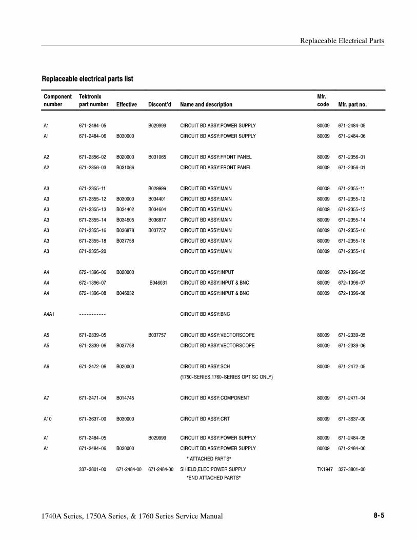
Replaceable Electrical Parts
1740A Series, 1750A Series, & 1760 Series Service Manual 8- 5
Replaceable electrical parts list
Component
number
Tektronix
part number Effective Discont’d Name and description
Mfr.
code Mfr. part no.
A1 671--2484--05 B029999 CIRCUIT BD ASSY:POWER SUPPLY 80009 671--2484--05
A1 671--2484--06 B030000 CIRCUIT BD ASSY:POWER SUPPLY 80009 671--2484--06
A2 671--2356--02 B020000 B031065 CIRCUIT BD ASSY:FRONT PANEL 80009 671--2356--01
A2 671--2356--03 B031066 CIRCUIT BD ASSY:FRONT PANEL 80009 671--2356--01
A3 671--2355--11 B029999 CIRCUIT BD ASSY:MAIN 80009 671--2355--11
A3 671--2355--12 B030000 B034401 CIRCUIT BD ASSY:MAIN 80009 671--2355--12
A3 671--2355--13 B034402 B034604 CIRCUIT BD ASSY:MAIN 80009 671--2355--13
A3 671--2355--14 B034605 B036877 CIRCUIT BD ASSY:MAIN 80009 671--2355--14
A3 671--2355--16 B036878 B037757 CIRCUIT BD ASSY:MAIN 80009 671--2355--16
A3 671--2355--18 B037758 CIRCUIT BD ASSY:MAIN 80009 671--2355--18
A3 671--2355--20 CIRCUIT BD ASSY:MAIN 80009 671--2355--18
A4 672--1396--06 B020000 CIRCUIT BD ASSY:INPUT 80009 672--1396--05
A4 672--1396--07 B046031 CIRCUIT BD ASSY:INPUT & BNC 80009 672--1396--07
A4 672--1396--08 B046032 CIRCUIT BD ASSY:INPUT & BNC 80009 672--1396--08
A4A1 -- -- -- -- -- -- -- -- -- -- -- CIRCUIT BD ASSY:BNC
A5 671--2339--05 B037757 CIRCUIT BD ASSY:VECTORSCOPE 80009 671--2339--05
A5 671--2339--06 B037758 CIRCUIT BD ASSY:VECTORSCOPE 80009 671--2339--06
A6 671--2472--06 B020000 CIRCUIT BD ASSY:SCH 80009 671--2472--05
(1750--SERIES,1760--SERIES OPT SC ONLY)
A7 671--2471--04 B014745 CIRCUIT BD ASSY:COMPONENT 80009 671--2471--04
A10 671--3637--00 B030000 CIRCUIT BD ASSY:CRT 80009 671--3637--00
A1 671--2484--05 B029999 CIRCUIT BD ASSY:POWER SUPPLY 80009 671--2484--05
A1 671--2484--06 B030000 CIRCUIT BD ASSY:POWER SUPPLY 80009 671--2484--06
* ATTACHED PARTS*
337--3801--00 671-2484-00 671-2484-00 SHIELD,ELEC:POWER SUPPLY TK1947 337--3801--00
*END ATTACHED PARTS*

Replaceable Electrical Parts
8- 6 1740A Series, 1750A Series, & 1760 Series Service Manual
Replaceable electrical parts list (Cont.)
Component
number Mfr. part no.
Mfr.
codeName and descriptionDiscont’dEffective
Tektronix
part number
A1C1 283--0429--00 CAP,FXD,CER DI:270PF,20%,2000V 18796 DHR12--Z5U271M--2
A1C2 281--0775--01 CAP,FXD,CERAMIC:MCL;0.1UF,20%,50V,Z5U,0.170 04222 SA105E104MAA
A1C3 283--0021--00 CAP,FXD,CER DI:0.001UF,20%,5000V TK2058 TCK45YS3H102M--A
A1C4 283--0639--01 CAP,FXD,MICA DI:56PF,1%,500V 09023 CDA15ED560F03
A1C5 283--0339--01 CAP,FXD,CERAMIC:MLC;0.22UF,10%,50V,X7R,0.300 X 0.300 TK2058 FK22X7R1H224K--T
A1C6 283--0261--00 CAP,FXD,CER DI:0.01UF,20%,4000V 18796 DHR28Z5U103M4KV
A1C7 283--0261--00 CAP,FXD,CER DI:0.01UF,20%,4000V 18796 DHR28Z5U103M4KV
A1C8 283--0261--00 CAP,FXD,CER DI:0.01UF,20%,4000V 18796 DHR28Z5U103M4KV
A1C9 285--1341--01 CAP,FXD,PLSTC:MTLZD FILM;0.1UF,20%,100V,POLYESTER TK1913 MKS 2 0.1UF 20%
A1C10 281--0775--01 CAP,FXD,CERAMIC:MCL;0.1UF,20%,50V,Z5U,0.170 04222 SA105E104MAA
A1C11 283--0000--04 CAP,FXD,CER DI:0.001UF,+100--0X,500V 18796 DD05--90HAY5U102
A1C12 283--0021--00 CAP,FXD,CER DI:0.001UF,20%,5000V TK2058 TCK45YS3H102M--A
A1C13 283--0189--00 CAP,FXD,CER DI:0.1UF,20%,400V 04222 SR508C104MAA
A1C14 285--1341--01 CAP,FXD,PLSTC:MTLZD FILM;0.1UF,20%100V,POLYESTER TK1913 MKS 2 0.1UF 20%
A1C15 290--1311--00 CAP,FXD,ALUM:10UF,20%,50V,ESR=1.4 OHM
(100KHZ,20C),5X11MM,105C,5000HRS
55680 UPL1H100MDH1TD
A1C16 283--0084--02 CAP,FXD,CER DI:270PF,5%,1000V,DISC 60705 562CRE102EF271J
A1C17 285--1341--01 CAP,FXD,PLSTC:MTLZD FILM;0.1UF,20%,100V,POLYESTER TK1913 MKS 2 0.1UF 20%
A1C18 283--0189--00 CAP,FXD,CER DI:0.1UF,20%,400V 04222 SR508C104MAA
A1C19 285--1341--01 CAP,FXD,PLSTC:MTLZD FILM;0.1UF,20%,100V,POLYESTER TK1913 MKS 2 0.1UF 20%
A1C20 283--0189--00 CAP,FXD,CER DI:0.1UF,20%,400V 04222 SR508C104MAA
A1C21 290--1311--00 CAP,FXD,ALUM:10UF,20%,50V,ESR=1.4 OHM
(100KHZ,20C),5X11MM,105C,5000HRS
55680 UPL1H100MDH1TD
A1C22 290--0939--00 CAP,FXD,ELCTLT:10UF,+100--10%,100V 62643 LX100VB10RM10X2
A1C23 285--1189--00 CAP,FXD,MTLZD:0.1 UF,5%,100 V 05292 PMT 3R .1J 100
A1C24 285--1328--00 CAP,FXD,PLSTC:MTLZD FILM;0.01UF,5%,2000V,POLYPROPY-
LENE,1.25X.95
TK1913 FKP1 .01/2000/5
A1C25 290--1310--00 CAP,FXD,ALUM:10UF,20%,160V,ESR=24.9 OHM
(120HZ,20C),LS=0.200 INCH,13X20MM,105C,5000HRS
0H1N5 CEJSM2C100M
A1C26 290--1311--00 CAP,FXD,ALUM:10UF,20%,50V,ESR=1.4 OHM
(100KHZ,20C),5X11MM,105C,5000HRS
55680 UPL1H100MDH1TD
A1C27 283--0339--01 CAP,FXD,CERAMIC:MLC;0.22UF,10%,50V,X7R,0.300 X 0.300 TK2058 FK22X7R1H224K--T
A1C28 281--0775--01 CAP,FXD,CERAMIC:MCL;0.1UF,20%,50V,Z5U,0.170 04222 SA105E104MAA
A1C29 290--1302--00 CAP,FXD,ALUM:1000UF,20%,35V,12.5 X 30MM(0.492 X 1.180) 0H1N5 CEEFM1V102M7
A1C30 290--1310--00 CAP,FXD,ALUM:10UF,20%,160V,ESR=24.9 OHM
(120HZ,20C),LS=0.200 INCH,13X20MM,105C,5000HRS
0H1N5 CEJSM2C100M
A1C31 290--1267--00 CAP,FXD,ALUM:560UF,20%,50V,ESR=0.40 OHM (100KHZ,20C) 0H1N5 CEEFM1H561M7
A1C32 290--0939--00 CAP,FXD,ELCTLT:10UF,+100--10%,100V 62643 LX100VB10RM10X2
A1C33 290--0939--00 CAP,FXD,ELCTLT:10UF,+100--10%,100V 62643 LX100VB10RM10X2

Replaceable Electrical Parts
1740A Series, 1750A Series, & 1760 Series Service Manual 8- 7
Replaceable electrical parts list (Cont.)
Component
number Mfr. part no.
Mfr.
codeName and descriptionDiscont’dEffective
Tektronix
part number
A1C34 290--1309--00 CAP,FXD,AL:100UF,20%,63V,10 X 20MM,RDL,105 DEG,L0W Z 0H1N5 CEEFM1J101M6--T4
A1C35 290--1314--00 CAP,FXD,ALUM:330UF,20%,63V,ESR=0.049 OHM
(100KHZ,20C),12.5X25MM,105C,LOW IMP
55680 UPL1J331MRH1TD
A1C36 290--1302--00 CAP,FXD,ALUM:1000UF,20%,35V,12.5 X 30MM(0.492 X 1.180) 0H1N5 CEEFM1V102M7
A1C37 290--1309--00 CAP,FXD,AL:100UF,20%,63V,10 X 20MM,RDL,105 DEG,L0W Z 0H1N5 CEEFM1J101M6--T4
A1C38 281--0775--01 CAP,FXD,CERAMIC:MCL;0.1UF,20%,50V,Z5U,0.170 04222 SA105E104MAA
A1C40 290--1309--00 CAP,FXD,AL:100UF,20%,63V,10 X 20MM,RDL,105 DEG,L0W Z 0H1N5 CEEFM1J101M6--T4
A1C41 290--1267--00 CAP,FXD,ALUM:560UF,20%,50V,ESR=0.40 OHM (100KHZ,20C) 0H1N5 CEEFM1H561M7
A1C42 281--0773--00 CAP,FXD,CERAMIC:MLC;0.01UF,10%,100V TK1743 CGB103KEX
A1C43 281--0775--01 CAP,FXD,CERAMIC:MCL;0.1UF,20%,50V,Z5U,0.170 04222 SA105E104MAA
A1C44 285--1420--00 CAP,FXD,PLSTC:FILM&FOIL;4700PF,63V,5% TK1913 FKP2 4700/63/5
A1C45 281--0775--01 CAP,FXD,CERAMIC:MCL;0.1UF,20%,50V,Z5U,0.170 04222 SA105E104MAA
A1C46 281--0775--01 CAP,FXD,CERAMIC:MCL;0.1UF,20%,50V,Z5U,0.170 04222 SA105E104MAA
A1C47 281--0813--00 CAP,FXD,CERAMIC:MLC;0.047UF,20%,50V,0.100 04222 SA105E473MAA
A1C48 283--0111--04 CAP,FXD,CER DI:0.1UF,20%,50V 04222 SR595C104MAAAP1
A1C49 281--0775--01 CAP,FXD,CERAMIC:MCL;0.1UF,20%,50V,Z5U,0.170 04222 SA105E104MAA
A1C51 285--1331--00 CAP,FXD,MTLZD:0.47UF,5%,400V TK1913 MKS4 .47/400/5
A1C52 285--1331--00 CAP,FXD,MTLZD:0.47UF,5%,400V TK1913 MKS4 .47/400/5
A1C53 281--0823--00 CAP,FXD,CER DI:470PF,10%,50V 04222 SA101A471KAA
A1C55 281--0786--00 CAP,FXD,CERAMIC:MLC;150PF,10%,100V,0.100 X0.170 04222 SA101A151KAA
A1C56 290--1315--00 CAP,FXD,ALUM:47UF,20%,35V,ESR=0.34 OHM
(100KHZ,20C),6X11MM,LOW IMP
55680 UPL1V470MEH1TD
A1C57 285--1251--00 CAP,FXD,PLSTC:0.033UF,10%,400VAC TK0515 PMR10 333 K400
A1C58 290--1264--00 CAP,FXD,ELCTLT:0.047F,--20%/+80%,5.5V,0.53OD 61058 PANASONIC EECF5
A1C59 285--1470--00 CAP,FXD,PLSTC:MTLZD FILM;330PF,1600VDC/500VAC TK1913 FKP1 330/1600/5
A1C60 285--1420--00 CAP,FXD,PLSTC:FILM&FOIL;4700PF,63V,5% TK1913 FKP2 4700/63/5
A1C61 281--0775--01 CAP,FXD,CERAMIC:MCL;0.1UF,20%,50V,Z5U,0.170 04222 SA105E104MAA
A1C62 290--1314--00 CAP,FXD,ALUM:330UF,20%,63V,ESR=0.049 OHM
(100KHZ,20C),12.5X25MM,105C,LOW IMP
55680 UPL1J331MRH1TD
A1C63 281--0775--01 CAP,FXD,CERAMIC:MCL;0.1UF,20%,50V,Z5U,0.170 04222 SA105E104MAA
A1C64 281--0775--01 CAP,FXD,CERAMIC:MCL;0.1UF,20%,50V,Z5U,0.170 04222 SA105E104MAA
A1C65 281--0775--01 CAP,FXD,CERAMIC:MCL;0.1UF,20%,50V,Z5U,0.170 04222 SA105E104MAA
A1C66 285--1246--00 CAP,FXD,PPR DI:0.022UF,20%,250VAC TK0515 PME 289 MB 5220
A1C67 281--0765--00 CAP,FXD,CER DI:100PF,5%,100V 04222 SA102A101JAA
A1C68 281--0765--00 CAP,FXD,CER DI:100PF,5%,100V 04222 SA102A101JAA
A1C69 281--0775--01 CAP,FXD,CERAMIC:MCL;0.1UF,20%,50V,Z5U,0.170 04222 SA105E104MAA
A1C70 281--0775--01 CAP,FXD,CERAMIC:MCL;0.1UF,20%,50V,Z5U,0.170 04222 SA105E104MAA

Replaceable Electrical Parts
8- 8 1740A Series, 1750A Series, & 1760 Series Service Manual
Replaceable electrical parts list (Cont.)
Component
number Mfr. part no.
Mfr.
codeName and descriptionDiscont’dEffective
Tektronix
part number
A1C71 290--1275--00 CAP,FXD,ALUM:330UF,20%,400V,35X35MM,105C 55680 LGQ2G331MHSC
A1C72 281--0765--00 CAP,FXD,CER DI:100PF,5%,100V 04222 SA102A101JAA
A1C74 285--1246--00 CAP,FXD,PPR DI:0.022UF,20%,250VAC TK0515 PME 289 MB 5220
A1C75 285--1222--00 CAP,FXD,PLSTC:0.068UF,20%,250V TK0515 PME 271 M 568
A1C76 281--0775--01 CAP,FXD,CERAMIC:MCL;0.1UF,20%,50V,Z5U,0.170 04222 SA105E104MAA
A1C77 283--0339--01 CAP,FXD,CERAMIC:MLC;0.22UF,10%,50V,X7R,0.300 X 0.300 TK2058 FK22X7R1H224K--T
A1CR1 152--0141--02 DIODE,SIG:ULTRA FAST;40V,150MA,4NS,2PF 27014 FDH9427
A1CR2 152--0061--00 DIODE,SIG:200V,0.1A,700NS,4.0PF 12969 PV122
A1CR3 152--0141--02 DIODE,SIG:ULTRA FAST;40V,150MA,4NS,2PF 27014 FDH9427
A1CR4 152--0061--00 DIODE,SIG:200V,0.1A,700NS,4.0PF 12969 PV122
A1CR5 152--0061--00 DIODE,SIG:200V,0.1A,700NS,4.0PF 12969 PV122
A1CR6 152--0061--00 DIODE,SIG:200V,0.1A,700NS,4.0PF 12969 PV122
A1CR7 152--0409--00 DIODE,RECT:FAST RCVRY;12KV,10MA,250NS 83701 CRVT150
A1CR8 152--0061--00 DIODE,SIG:200V,0.1A,700NS,4.0PF 12969 PV122
A1CR9 152--0061--00 DIODE,SIG:200V,0.1A,700NS,4.0PF 12969 PV122
A1CR10 152--0400--00 DIODE,RECT:FAST RCVRY;400V,1A,200NS 0LUA3 1N4936
A1CR11 152--0400--00 DIODE,RECT:FAST RCVRY;400V,1A,200NS 0LUA3 1N4936
A1CR12 152--0141--02 DIODE,SIG:ULTRA FAST;40V,150MA,4NS,2PF 27014 FDH9427
A1CR13 152--0141--02 DIODE,SIG:ULTRA FAST;40V,150MA,4NS,2PF 27014 FDH9427
A1CR14 152--0141--02 DIODE,SIG:ULTRA FAST;40V,150MA,4NS,2PF 27014 FDH9427
A1CR15 152--0400--00 DIODE,RECT:FAST RCVRY;400V,1A,200NS 0LUA3 1N4936
A1CR16 152--0720--00 DIODE,RECT:ULTRA FAST;200V,8A,25NS,100A IF SM 0LUA3 BYW29--200
*ATTACHED PARTS*
210--0406--00 NUT,PLAIN,HEX:4--40 X 0.188,BRS CD PL 73743 12161--50
211--0008--00 SCREW,MACHINE:4--40 X 0.25,PNH,STL TK0435 ORDER BY DESC
214--3841--00 HEAT SINK,SEMIC:XTR,TO--220;VERTICALMOUNT,(2)
SOLDERABLE TABS,ALUMINUM,BLACK ANODIZE
13103 6021PB
*END ATTACHED PARTS*
A1CR17 152--0720--00 DIODE,RECT:ULTRA FAST;200V,8A,25NS,100A IF SM 0LUA3 BYW29--200
*ATTACHED PARTS*
210--0406--00 NUT,PLAIN,HEX:4--40 X 0.188,BRS CD PL 73743 12161--50
211--0008--00 SCREW,MACHINE:4--40 X 0.25,PNH,STL TK0435 ORDER BY DESC
214--3841--00 HEAT SINK,SEMIC:XTR,TO--220;VERTICALMOUNT,(2)
SOLDERABLE TABS,ALUMINUM,BLACK ANODIZE
13103 6021PB
*END ATTACHED PARTS*
A1CR18 152--0720--00 DIODE,RECT:ULTRA FAST;200V,8A,25NS,100A IF SM 0LUA3 BYW29--200
*ATTACHED PARTS*
210--0406--00 NUT,PLAIN,HEX:4--40 X 0.188,BRS CD PL 73743 12161--50

Replaceable Electrical Parts
1740A Series, 1750A Series, & 1760 Series Service Manual 8- 9
Replaceable electrical parts list (Cont.)
Component
number Mfr. part no.
Mfr.
codeName and descriptionDiscont’dEffective
Tektronix
part number
211--0008--00 SCREW,MACHINE:4--40 X 0.25,PNH,STL TK0435 ORDER BY DESC
214--3841--00 HEAT SINK,SEMIC:XTR,TO--220;VERTICALMOUNT,(2)
SOLDERABLE TABS,ALUMINUM,BLACK ANODIZE
13103 6021PB
*END ATTACHED PARTS*
A1CR19 152--0863--00 DIODE,RECT:ULTRA FAST;600V,1A,30NS,SOFT RCVRY 0LUA3 BYV26C
A1CR20 152--0141--02 DIODE,SIG:ULTRA FAST;40V,150MA,4NS,2PF 27014 FDH9427
A1CR21 152--0141--02 DIODE,SIG:ULTRA FAST;40V,150MA,4NS,2PF 27014 FDH9427
A1CR22 152--0400--00 DIODE,RECT:FAST RCVRY;400V,1A,200NS 0LUA3 1N4936
A1CR23 152--0897--00 DIODE,RECT:FAST RCVRY;1000V,1.5A,300NS,SOFT RCVRY 0LUA3 BYV96E
A1CR24 152--0863--00 DIODE,RECT:ULTRA FAST;600V,1A,30NS,SOFT RCVRY 0LUA3 BYV26C
A1CR25 152--0897--00 DIODE,RECT:FAST RCVRY;1000V,1.5A,300NS,SOFT RCVRY 0LUA3 BYV96E
A1CR26 152--0400--00 DIODE,RECT:FAST RCVRY;400V,1A,200NS 0LUA3 1N4936
A1CR27 152--0141--02 DIODE,SIG:ULTRA FAST;40V,150MA,4NS,2PF 27014 FDH9427
A1CR28 152--0863--00 DIODE,RECT:ULTRA FAST;600V,1A,30NS,SOFT RECOVERY 0LUA3 BYV26C
A1CR29 152--0141--02 DIODE,SIG:ULTRA FAST;40V,150MA,4NS,2PF 27014 FDH9427
A1CR30 152--0141--02 DIODE,SIG:ULTRA FAST;40V,150MA,4NS,2PF 27014 FDH9427
A1CR31 152--0141--02 DIODE,SIG:ULTRA FAST;40V,150MA,4NS,2PF 27014 FDH9427
A1CR32 152--1165--00 DIODE,RECT:ULTRA FAST;600V,4A,50NS 04713 MUR460RL
A1CR33 152--1165--00 DIODE,RECT:ULTRA FAST;600V,4A,50NS 04713 MUR460RL
A1CR34 152--1165--00 DIODE,RECT:ULTRA FAST;600V,4A,50NS 04713 MUR460RL
A1CR35 152--1165--00 DIODE,RECT:ULTRA FAST;600V,4A,50NS 04713 MUR460RL
A1DS1 150--0050--00 LAMP,GLOW:135V MAX,1.9MA,C2A--T,WIRE LEAD 0J9R2 NE--2Q--11R--T
A1DS2 150--0050--00 LAMP,GLOW:135V MAX,1.9MA,C2A--T,WIRE LEAD 0J9R2 NE--2Q--11R--T
A1DS3 150--0050--00 LAMP,GLOW:135V MAX,1.9MA,C2A--T,WIRE LEAD 0J9R2 NE--2Q--11R--T
A1DS4 150--0050--00 LAMP,GLOW:135V MAX,1.9MA,C2A--T,WIRE LEAD 0J9R2 NE--2Q--11R--T
A1DS5 150--0050--00 LAMP,GLOW:135V MAX,1.9MA,C2A--T,WIRE LEAD 0J9R2 NE--2Q--11R--T
A1DS6 150--1152--00 DIO,OPTO:LED;HIGH EFFIC. RED,635NM,INTEGRAL RES 50434 HLMP--1600--002
A1DS7 150--0050--00 LAMP,GLOW:135V MAX,1.9MA,C2A--T,WIRE LEAD 0J9R2 NE--2Q--11R--T
A1F1 159--0021--00 FUSE,CARTRIDGE:3AG,2A,250V,FAST BLOW 71400 AGC--2
*MOUNTING PARTS*
200--2264--00 CAP,FUSEHOLDER:3AG FUSES 61935 FEK 031 1666
204--0906--00 BODY,FUSEHOLDER:3AG & 5 X 20MM FUSES 61935 TYPE FAU 031.35
*END MOUNTING PARTS*
A1J1 131--5338--00 CONN,HDR:PCB/WIREWRAP;MALE,STR,1 X 7,0.15CTR,
0.230 MLG X 0.285 TAIL,30 GLD,SIDE BY SIDE STACKABLE
22526 65561--107
A1J2 131--5337--00 CONN,HDR:PCB/WIREWRAP;MALE,STR,1 X 4,0.150 22526 65561--104
A1J3 131--4794--00 CONN,HDR:PCB;MALE,STR,1 X 2,0.1 CTR,0.235
MLG X 0.112 TAIL,30GOLD,0.035 DIA PCB
53387 2402--6112 UB
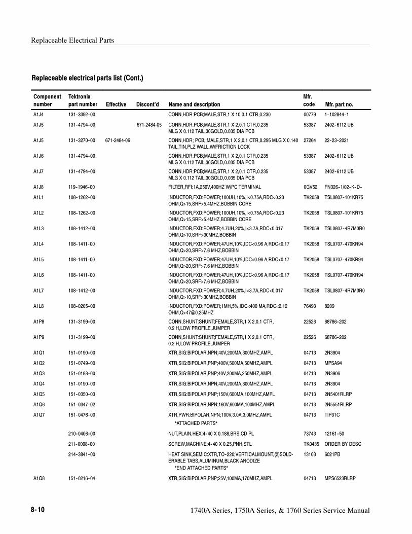
Replaceable Electrical Parts
8- 10 1740A Series, 1750A Series, & 1760 Series Service Manual
Replaceable electrical parts list (Cont.)
Component
number Mfr. part no.
Mfr.
codeName and descriptionDiscont’dEffective
Tektronix
part number
A1J4 131--3392--00 CONN,HDR:PCB;MALE,STR,1 X 10,0.1 CTR,0.230 00779 1--102844--1
A1J5 131--4794--00 671-2484-05 CONN,HDR:PCB;MALE,STR,1 X 2,0.1 CTR,0.235
MLG X 0.112 TAIL,30GOLD,0.035 DIA PCB
53387 2402--6112 UB
A1J5 131--3270--00 671-2484-06 CONN,HDR; PCB,;MALE,STR,1 X 2,0.1 CTR,0.295 MLG X 0.140
TAIL,TIN,PLZ WALL,W/FRICTION LOCK
27264 22--23--2021
A1J6 131--4794--00 CONN,HDR:PCB;MALE,STR,1 X 2,0.1 CTR,0.235
MLG X 0.112 TAIL,30GOLD,0.035 DIA PCB
53387 2402--6112 UB
A1J7 131--4794--00 CONN,HDR:PCB;MALE,STR,1 X 2,0.1 CTR,0.235
MLG X 0.112 TAIL,30GOLD,0.035 DIA PCB
53387 2402--6112 UB
A1J8 119--1946--00 FILTER,RFI:1A,250V,400HZ W/PC TERMINAL 0GV52 FN326--1/02--K--D--
A1L1 108--1262--00 INDUCTOR,FXD:POWER;100UH,10%,I<0.75A,RDC<0.23
OHM,Q>15,SRF>5.4MHZ,BOBBIN CORE
TK2058 TSL0807--101KR75
A1L2 108--1262--00 INDUCTOR,FXD:POWER;100UH,10%,I<0.75A,RDC<0.23
OHM,Q>15,SRF>5.4MHZ,BOBBIN CORE
TK2058 TSL0807--101KR75
A1L3 108--1412--00 INDUCTOR,FXD:POWER;4.7UH,20%,I<3.7A,RDC<0.017
OHM,Q>10,SRF>30MHZ,BOBBIN
TK2058 TSL0807--4R7M3R0
A1L4 108--1411--00 INDUCTOR,FXD:POWER;47UH,10%,IDC<0.96 A,RDC<0.17
OHM,Q>20,SRF>7.6 MHZ,BOBBIN
TK2058 TSL0707--470KR94
A1L5 108--1411--00 INDUCTOR,FXD:POWER;47UH,10%,IDC<0.96 A,RDC<0.17
OHM,Q>20,SRF>7.6 MHZ,BOBBIN
TK2058 TSL0707--470KR94
A1L6 108--1411--00 INDUCTOR,FXD:POWER;47UH,10%,IDC<0.96 A,RDC<0.17
OHM,Q>20,SRF>7.6 MHZ,BOBBIN
TK2058 TSL0707--470KR94
A1L7 108--1412--00 INDUCTOR,FXD:POWER;4.7UH,20%,I<3.7A,RDC<0.017
OHM,Q>10,SRF>30MHZ,BOBBIN
TK2058 TSL0807--4R7M3R0
A1L8 108--0205--00 INDUCTOR,FXD:POWER;1MH,5%,IDC<400 MA,RDC<2.12
OHM,Q>[email protected]
76493 8209
A1P8 131--3199--00 CONN,SHUNT:SHUNT;FEMALE,STR,1 X 2,0.1 CTR,
0.2 H,LOW PROFILE,JUMPER
22526 68786--202
A1P9 131--3199--00 CONN,SHUNT:SHUNT;FEMALE,STR,1 X 2,0.1 CTR,
0.2 H,LOW PROFILE,JUMPER
22526 68786--202
A1Q1 151--0190--00 XTR,SIG:BIPOLAR,NPN;40V,200MA,300MHZ,AMPL 04713 2N3904
A1Q2 151--0749--00 XTR,SIG:BIPOLAR,PNP;400V,500MA,50MHZ,AMPL 04713 MPSA94
A1Q3 151--0188--00 XTR,SIG:BIPOLAR,PNP;40V,200MA,250MHZ,AMPL 04713 2N3906
A1Q4 151--0190--00 XTR,SIG:BIPOLAR,NPN;40V,200MA,300MHZ,AMPL 04713 2N3904
A1Q5 151--0350--03 XTR,SIG:BIPOLAR,PNP;150V,600MA,100MHZ,AMPL 04713 2N5401RLRP
A1Q6 151--0347--02 XTR,SIG:BIPOLAR,NPN;160V,600MA,100MHZ,AMPL 04713 2N5551RLRP
A1Q7 151--0476--00 XTR,PWR:BIPOLAR,NPN;100V,3.0A,3.0MHZ,AMPL 04713 TIP31C
*ATTACHED PARTS*
210--0406--00 NUT,PLAIN,HEX:4--40 X 0.188,BRS CD PL 73743 12161--50
211--0008--00 SCREW,MACHINE:4--40 X 0.25,PNH,STL TK0435 ORDER BY DESC
214--3841--00 HEAT SINK,SEMIC:XTR,TO--220;VERTICALMOUNT,(2)SOLD-
ERABLE TABS,ALUMINUM,BLACK ANODIZE
13103 6021PB
*END ATTACHED PARTS*
A1Q8 151--0216--04 XTR,SIG:BIPOLAR,PNP;25V,100MA,170MHZ,AMPL 04713 MPS6523RLRP

Replaceable Electrical Parts
1740A Series, 1750A Series, & 1760 Series Service Manual 8- 11
Replaceable electrical parts list (Cont.)
Component
number Mfr. part no.
Mfr.
codeName and descriptionDiscont’dEffective
Tektronix
part number
A1Q9 151--0188--00 XTR,SIG:BIPOLAR,PNP;40V,200MA,250MHZ,AMPL 04713 2N3906
A1Q10 151--0190--00 XTR,SIG:BIPOLAR,NPN;40V,200MA,300MHZ,AMPL 04713 2N3904
A1Q11 151--0528--00 THYRISTOR,PWR:BIPOLAR,SCR;50V,16A RMS,PHASE 04713 2N6400
A1Q12 151--0188--00 XTR,SIG:BIPOLAR,PNP;40V,200MA,250MHZ,AMPL 04713 2N3906
A1Q13 151--0190--00 XTR,SIG:BIPOLAR,NPN;40V,200MA,300MHZ,AMPL 04713 2N3904
A1Q14 151--1286--00 XTR,PWR:MOS,N--CH;800V,4.0A,3.0 OHM 0LUA3 BUK456--800A
*ATTACHED PARTS*
210--0406--00 NUT,PLAIN,HEX:4--40 X 0.188,BRS CD PL 73743 12161--50
211--0008--00 SCREW,MACHINE:4--40 X 0.25,PNH,STL TK0435 ORDER BY DESC
214--4197--00 HTSK:XTR,T0=218,ALW/SOLDERABLE ROLL PINS,5298B 13103 6298B MODIFIED
*END ATTACHED PARTS*
A1Q15 151--0188--00 XTR,SIG:BIPOLAR,PNP;40V,200MA,250MHZ,AMPL 04713 2N3906
A1R1 301--0225--02 RES,FXD,CMPSN:2.2M OHM,5%,0.5W 50139 EB2255
A1R2 303--0155--00 RES,FXD,CMPSN:1.5M OHM,5%,1W 50139 GB1555
A1R3 303--0155--00 RES,FXD,CMPSN:1.5M OHM,5%,1W 50139 GB1555
A1R4 303--0155--00 RES,FXD,CMPSN:1.5M OHM,5%,1W 50139 GB1555
A1R5 322--3344--00 B029999 RES,FXD,FILM:37.4K OHM,1%,0.2W,TC=T0MI,SM BODY 91637 CCF501G37401F
A1R5 322--3329--00 B030000 RES,FXD,FILM; 26.1K OHM.1%,0.2W,TC=T0 MI,SMALL BODY 91637 CCF50--2612F--R36
A1R6 322--3251--00 RES,FXD,FILM:4.02K OHM,1%,0.2W,TC=T0TAPED & 91637 CCF501G40200F
A1R8 322--3097--00 RES,FXD:METAL FILM;100 OHM,1%,0.2W,TC=100 PPM 91637 CCF501G100R0F
A1R9 311--1256--00 RES,VAR,TRMR:CERMET;2.5M OHM,10%,0.5W,0.375 32997 3386F--1--255
A1R10 322--3385--00 RES,FXD:METAL FILM;100K OHM,1%,0.2W,TC=100 PPM 91637 CCF501G10002F
A1R11 322--3097--00 RES,FXD:METAL FILM;100 OHM,1%,0.2W,TC=100 PPM 91637 CCF501G100R0F
A1R12 322--3097--00 RES,FXD:METAL FILM;100 OHM,1%,0.2W,TC=100 PPM 91637 CCF501G100R0F
A1R13 303--0155--00 RES,FXD,CMPSN:1.5M OHM,5%,1W 50139 GB1555
A1R14 322--3339--00 RES,FXD:METAL FILM;33.2K OHM,1%,0.2W,TC=100 91637 CCF50--2--G3322FT
A1R15 322--3481--00 RES,FXD,FILM:1M OHM.1%,0.2W,TC=T0MI,SMALL BODY 91637 CCF501G10003F
A1R16 315--0101--03 RES,FXD,CMPSN:100 OHM,5%,0.25W 50139 CB1015
A1R17 322--3254--00 RES,FXD,FILM:4.32K OHM,1%,0.2W,TC=T0MI,SM BODY 91637 CCF502G4321FT
A1R18 322--3162--00 RES,FXD:METAL FILM;475 OHM,1%,0.2W,TC=100 PPM 91637 CCF50G475R0F
A1R19 315--0223--03 B030000 RES,FXD,CMPSN:22K OHM,5%,0.25 WALLEN BRADLEY 50139 CB2235 ALLEN BR
A1R20 315--0102--03 RES,FXD,CMPSN:1K OHM,5%,0.25W 50139 CB1025 (CARD PA
A1R21 322--3306--00 RES,FXD:METAL FILM;15K OHM,1%,0.2W,TC=100 PPM 91637 CCF50--2--G1502F
A1R22 322--3105--00 RES,FXD:METAL FILM;121 OHM,1%,0.2W,TC=100 PPM 91637 CCF501G121ROF
A1R23 322--3385--00 RES,FXD:METAL FILM;100K OHM,1%,0.2W,TC=100 PPM 91637 CCF501G10002F
A1R24 322--3222--00 RES,FXD:METAL FILM;2K OHM,1%,0.2W,TC=100 PPM 91637 CCF501G20000F

Replaceable Electrical Parts
8- 12 1740A Series, 1750A Series, & 1760 Series Service Manual
Replaceable electrical parts list (Cont.)
Component
number Mfr. part no.
Mfr.
codeName and descriptionDiscont’dEffective
Tektronix
part number
A1R25 322--3034--00 RES,FXD:METAL FILM;22.1 OHM,1%,0.2W,TC=100 PPM 91637 CCF50--2--G22R10F
A1R26 315--0470--03 RES,FXD,CMPSN:47 OHM,5%,0.25W 50139 CB4705
A1R27 322--3162--00 RES,FXD:METAL FILM;475 OHM,1%,0.2W,TC=100 PPM 91637 CCF50G475R0F
A1R28 322--3222--00 RES,FXD:METAL FILM;2K OHM,1%,0.2W,TC=100 PPM 91637 CCF501G20000F
A1R29 322--3001--00 RES,FXD:METAL FILM;10 OHM,1%,0.2W,TC=100 PPM 91637 CCF501G10R00F
A1R30 315--0226--01 RES,FXD,CMPSN:22 M OHM,5%,0.25WALLEN BRADLEY 50139 CB2265
A1R31 315--0471--03 RES,FXD,CMPSN:470 OHM,5%,0.25W 50139 CB4715
A1R32 315--0471--03 RES,FXD,CMPSN:470 OHM,5%,0.25W 50139 CB4715
A1R33 322--3354--00 RES,FXD:METAL FILM;47.5K OHM,1%,0.2W,TC=100 91637 CCF501G47501F
A1R34 315--0471--03 RES,FXD,CMPSN:470 OHM,5%,0.25W 50139 CB4715
A1R35 322--3273--00 RES,FXD:METAL FILM;6.81K OHM,1%,0.2W,TC=100 91637 CCF50--2--G68100F
A1R36 315--0102--03 RES,FXD,CMPSN:1K OHM,5%,0.25W 50139 CB1025 (CARD PA
A1R37 322--3385--00 B029999 RES,FXD:METAL FILM;100K OHM,1%,0.2W,TC=100 PPM 91637 CCF501G10002F
A1R37 322--3373--00 B030000
A1R38 311--2239--00 RES,VAR,TRMR:CERMET;100K OHM,20%,0.5W,0.197 TK2073 GF06UT2 104 M L
A1R39 322--3001--00 RES,FXD:METAL FILM;10 OHM,1%,0.2W,TC=100 PPM 91637 CCF501G10R00F
A1R40 322--3239--00 RES,FXD,FILM:3.01K OHM,1%,0.2W,TC=T0MI,SM BODY 91637 CCF501G30100F
A1R41 322--3435--00 RES,FXD:METAL FILM;332K OHM,1%,0.2W,TC=100 PPM 91637 CCF50--2--33202FT
A1R42 311--2240--00 RES,VAR,NONWW:TRMR,200K OHM,20%,0.5W LINEAR TK2073 GF06UT2 204 M L
A1R43 322--3273--00 RES,FXD:METAL FILM;6.81K OHM,1%,0.2W,TC=100 91637 CCF50--2--G68100F
A1R44 311--2239--00 B029999 RES,VAR,TRMR:CERMET;100K OHM,20%,0.5W,0.197 TK2073 GF06UT2 104 M L
A1R44 311--2237--00 B030000 HARDWARE KIT; REPLACEMENT;K4000 TK2476 020--2363--00
A1R45 322--3001--00 RES,FXD:METAL FILM;10 OHM,1%,0.2W,TC=100 PPM 91637 CCF501G10R00F
A1R46 322--3322--00 RES,FXD:METAL FILM;22.1K OHM,1%,0.2W,TC=100 91637 CCF501G22101F
A1R47 322--3001--00 RES,FXD:METAL FILM;10 OHM,1%,0.2W,TC=100 PPM 91637 CCF501G10R00F
A1R48 322--3001--00 RES,FXD:METAL FILM;10 OHM,1%,0.2W,TC=100 PPM 91637 CCF501G10R00F
A1R49 322--3024--00 RES,FXD,FILM:17.4 OHM,1%,0.2W,TC=T0,SMALL BODY 91637 CCF50--2--G17R40F
A1R50 322--3322--00 RES,FXD:METAL FILM;22.1K OHM,1%,0.2W,TC=100 91637 CCF501G22101F
A1R51 322--3001--00 RES,FXD:METAL FILM;10 OHM,1%,0.2W,TC=100 PPM 91637 CCF501G10R00F
A1R52 322--3193--00 RES,FXD:METAL FILM;1K OHM,1%,0.2W,TC=100 PPM 91637 CCF501G10000F
A1R53 311--2239--00 RES,VAR,TRMR:CERMET;100K OHM,20%,0.5W,0.197 TK2073 GF06UT2 104 M L
A1R54 322--3193--00 RES,FXD:METAL FILM;1K OHM,1%,0.2W,TC=100 PPM 91637 CCF501G10000F
A1R55 322--3481--00 RES,FXD,FILM:1M OHM.1%,0.2W,TC=T0MI,SMALL BODY 91637 CCF501G10003F
A1R56 322--3193--00 RES,FXD:METAL FILM;1K OHM,1%,0.2W,TC=100 PPM 91637 CCF501G10000F
A1R57 322--3235--00 RES,FXD:METAL FILM;2.74K OHM,1%,0.2W,TC=100 91637 CCF501G27400F
A1R58 322--3193--00 RES,FXD:METAL FILM;1K OHM,1%,0.2W,TC=100 PPM 91637 CCF501G10000F

Replaceable Electrical Parts
1740A Series, 1750A Series, & 1760 Series Service Manual 8- 13
Replaceable electrical parts list (Cont.)
Component
number Mfr. part no.
Mfr.
codeName and descriptionDiscont’dEffective
Tektronix
part number
A1R59 322--3193--00 RES,FXD:METAL FILM;1K OHM,1%,0.2W,TC=100 PPM 91637 CCF501G10000F
A1R60 322--3260--00 RES,FXD,FILM:4.99K OHM,1%,0.2W,TC=T0 91637 CCF501G49900F
A1R61 322--3261--00 RES,FXD,FILM:5.11K OHM,1%,0.2W,TC=T0MI,SM BODY 91637 CCF50G5111FT
A1R62 322--3097--00 RES,FXD:METAL FILM;100 OHM,1%,0.2W,TC=100 PPM 91637 CCF501G100R0F
A1R63 322--3001--00 RES,FXD:METAL FILM;10 OHM,1%,0.2W,TC=100 PPM 91637 CCF501G10R00F
A1R64 322--3001--00 RES,FXD:METAL FILM;10 OHM,1%,0.2W,TC=100 PPM 91637 CCF501G10R00F
A1R65 322--3201--00 RES,FXD:METAL FILM;1.21K OHM,1%,0.2W,TC=100 91637 CCF501G12100F
A1R66 322--3385--00 RES,FXD:METAL FILM;100K OHM,1%,0.2W,TC=100 PPM 91637 CCF501G10002F
A1R67 322--3385--00 RES,FXD:METAL FILM;100K OHM,1%,0.2W,TC=100 PPM 91637 CCF501G10002F
A1R68 322--3339--00 RES,FXD:METAL FILM;33.2K OHM,1%,0.2W,TC=100 91637 CCF50--2--G3322FT
A1R69 307--0106--00 RES,FXD,CMPSN:4.7 OHM,5%,0.25W 50139 CB47G5
A1R70 303--0100--00 RES,FXD,CMPSN:10 OHM,5%,1W,COMPOSITION OR FILM 24546 FP32 OR FP1 10
A1R71 322--3222--00 RES,FXD:METAL FILM;2K OHM,1%,0.2W,TC=100 PPM 91637 CCF501G20000F
A1R72 322--3289--00 RES,FXD:METAL FILM;10K OHM,1%,0.2W,TC=100 PPM 91637 CCF50G10001F
A1R73 311--2238--00 RES,VAR,TRMR:CERMET;50K OHM,20%,0.5W,0.197
SQ,SIDE ADJUST
TK2073 GF06UT2 503 M L
A1R74 322--3289--00 RES,FXD:METAL FILM;10K OHM,1%,0.2W,TC=100 PPM 91637 CCF50G10001F
A1R75 322--3306--00 RES,FXD:METAL FILM;15K OHM,1%,0.2W,TC=100 PPM 91637 CCF50--2--G1502F
A1R76 322--3222--00 RES,FXD:METAL FILM;2K OHM,1%,0.2W,TC=100 PPM 91637 CCF501G20000F
A1R77 322--3352--00 RES,FXD,FILM:45.3K OHM,1%,0.2W,TC=T0MI,SM BODY 91637 CCF501G45301F
A1R78 322--3225--00 RES,FXD,FILM:2.15K OHM,1%,0.2W,TC=T0 91637 CCF501G21500F
A1R79 322--3193--00 RES,FXD:METAL FILM;1K OHM,1%,0.2W,TC=100 PPM 91637 CCF501G10000F
A1R80 322--3327--00 RES,FXD,FILM:24.9K OHM,1%,0.2W,TC=T0MI,SM BODY 91637 CCF50--2--G24901F
A1R81 322--3322--00 RES,FXD:METAL FILM;22.1K OHM,1%,0.2W,TC=100 91637 CCF501G22101F
A1R82 322--3322--00 RES,FXD:METAL FILM;22.1K OHM,1%,0.2W,TC=100 91637 CCF501G22101F
A1R83 322--3418--00 RES,FXD:METAL FILM;221K OHM,1%,0.2W,TC=100 PPM 91637 CCF501G22102F
A1R84 322--3235--00 RES,FXD:METAL FILM;2.74K OHM,1%,0.2W,TC=100 91637 CCF501G27400F
A1R85 322--3481--00 RES,FXD,FILM:1M OHM.1%,0.2W,TC=T0MI,SMALL BODY 91637 CCF501G10003F
A1R86 322--3254--00 RES,FXD,FILM:4.32K OHM,1%,0.2W,TC=T0MI,SM BODY 91637 CCF502G4321FT
A1R87 322--3289--00 RES,FXD:METAL FILM;10K OHM,1%,0.2W,TC=100 PPM 91637 CCF50G10001F
A1R88 305--0242--00 RES,FXD,CMPSN:2.4K OHM,5%,2W 11502 GF--3 OR GS--3 24
A1R89 322--3369--00 RES,FXD:METAL FILM;68.1K OHM,1%,0.2W,TC=100 57668 CRB20 FXE 68R1
A1R90 308--0793--00 RES,FXD:0.51 OHM,5%,1WTC=150PPM/DEG C,MI 75042 BW20 .51OHM 5PE
A1R91 322--3193--00 RES,FXD:METAL FILM;1K OHM,1%,0.2W,TC=100 PPM 91637 CCF501G10000F
A1R92 322--3205--00 RES,FXD,FILM:1.33K OHM,1%,0.2W,TC=T0 91637 CCF501G13300F
A1R93 322--3121--00 RES,FXD:METAL FILM;178 OHM,1%,0.2W,TC=100 PPM 91637 CCF501G178R0F

Replaceable Electrical Parts
8- 14 1740A Series, 1750A Series, & 1760 Series Service Manual
Replaceable electrical parts list (Cont.)
Component
number Mfr. part no.
Mfr.
codeName and descriptionDiscont’dEffective
Tektronix
part number
A1R94 322--3347--00 RES,FXD,FILM:40.2K OHM,1%,0.2W,TC=T0MI,SM BODY 91637 CCF50--2--G40201F
A1R95 322--3260--00 RES,FXD,FILM:4.99K OHM,1%,0.2W,TC=T0 91637 CCF501G49900F
A1R96 322--3034--00 RES,FXD:METAL FILM;22.1 OHM,1%,0.2W,TC=100 PPM 91637 CCF50--2--G22R10F
A1R97 322--3226--00 RES,FXD:METAL FILM;2.21K OHM,1%,0.2W,TC=100 91637 CCF501G22100F
A1R98 322--3256--00 RES,FXD,FILM:4.53K OHM,1%,0.2W,TC=T0MI,SM BODY 91637 CCF50--2--G4531FT
A1R99 322--3222--00 RES,FXD:METAL FILM;2K OHM,1%,0.2W,TC=100 PPM 91637 CCF501G20000F
A1R100 322--3385--00 RES,FXD:METAL FILM;100K OHM,1%,0.2W,TC=100 PPM 91637 CCF501G10002F
A1R101 322--3222--00 RES,FXD:METAL FILM;2K OHM,1%,0.2W,TC=100 PPM 91637 CCF501G20000F
A1R102 322--3193--00 RES,FXD:METAL FILM;1K OHM,1%,0.2W,TC=100 PPM 91637 CCF501G10000F
A1R103 322--3289--00 RES,FXD:METAL FILM;10K OHM,1%,0.2W,TC=100 PPM 91637 CCF50G10001F
A1R104 322--3435--00 RES,FXD:METAL FILM;332K OHM,1%,0.2W,TC=100 PPM 91637 CCF50--2--33202FT
A1R105 322--3431--00 RES,FXD,FILM:301K OHM,1%,0.2W,TC=T0,SMALL BODY 91637 CCF501G30102F
A1R106 322--3339--00 RES,FXD:METAL FILM;33.2K OHM,1%,0.2W,TC=100 91637 CCF50--2--G3322FT
A1R107 322--3239--00 RES,FXD,FILM:3.01K OHM,1%,0.2W,TC=T0MI,SM BODY 91637 CCF501G30100F
A1R108 322--3222--00 RES,FXD:METAL FILM;2K OHM,1%,0.2W,TC=100 PPM 91637 CCF501G20000F
A1R109 322--3431--00 RES,FXD,FILM:301K OHM,1%,0.2W,TC=T0,SMALL BODY 91637 CCF501G30102F
A1R110 322--3322--00 RES,FXD:METAL FILM;22.1K OHM,1%,0.2W,TC=100 91637 CCF501G22101F
A1R111 322--3351--00 RES,FXD:METAL FILM;44.2K OHM,1%,0.2W,TC=100 91637 CCF501G4422FT
A1R112 322--3452--00 RES,FXD,FILM:499K OHM,1%,0.2W,TC=TOMI,SMALL 91637 CCF50--2--G4993FT
A1R113 322--3452--00 RES,FXD,FILM:499K OHM,1%,0.2W,TC=TOMI,SMALL 91637 CCF50--2--G4993FT
A1R114 322--3339--00 RES,FXD:METAL FILM;33.2K OHM,1%,0.2W,TC=100 91637 CCF50--2--G3322FT
A1R115 322--3401--00 RES,FXD,FILM:147K OHM,1%,0.2W,TC=T0MI,SMALL 57668 CRB20 FXE 147K
A1R116 308--0290--00 RES,FXD,WW:8 OHM,5%,5W 91637 CW52--8R000J T/R
A1R117 322--3393--00 RES,FXD:METAL FILM;121K OHM,1%,0.2W,TC=100 PPM 91637 CCF501G12102F
A1R118 322--3393--00 RES,FXD:METAL FILM;121K OHM,1%,0.2W,TC=100 PPM 91637 CCF501G12102F
A1R119 305--0154--00 RES,FXD,CMPSN:150K OHM,5%,2W 50139 HB1545
A1R120 306--0104--00 RES,FXD,CMPSN:100K OHM,10%,2W 24546 FP42 OR FP2 100
A1R121 305--0154--00 RES,FXD,CMPSN:150K OHM,5%,2W 50139 HB1545
A1R122 306--0104--00 RES,FXD,CMPSN:100K OHM,10%,2W 24546 FP42 OR FP2 100
A1R123 307--0353--00 RES,THERMAL:5 OHM,10% 15454 5DA5R0K--RO--220--
A1R124 322--3322--00 RES,FXD:METAL FILM;22.1K OHM,1%,0.2W,TC=100 91637 CCF501G22101F
A1R125 322--3481--00 RES,FXD,FILM:1M OHM.1%,0.2W,TC=T0MI,SMALL BODY 91637 CCF501G10003F
A1R126 322--3254--00 RES,FXD,FILM:4.32K OHM,1%,0.2W,TC=T0MI,SM BODY 91637 CCF502G4321FT
A1T1 120--1695--00 TRANSFORMER,PWR:HIGH VOLTAGE,FEEDBACK 3V,
RESONANT 231V, 100V 1MA,2750V 3.3MA, 6.3V 86MA
75498 120--1695--00

Replaceable Electrical Parts
1740A Series, 1750A Series, & 1760 Series Service Manual 8- 15
Replaceable electrical parts list (Cont.)
Component
number Mfr. part no.
Mfr.
codeName and descriptionDiscont’dEffective
Tektronix
part number
A1T2 120--1532--00 TRANSFORMER,RF:TOROID,ISOLATION,RATIO 1:1,IND
100--300 UH, DCR 1.5 OHM POTTED, PKG 0.8 X 0.65,0.55
HIGH
75498 128--8036--01
A1T3 120--1921--00 TRANSFORMER,RF:PCB;INPUT,[email protected],[email protected],
[email protected],OUTPUT +/-- [email protected],5V@2A,[email protected],
PRIIND 280UH
75498 129--2023--EB
A1TP1 214--4085--00 TERM,TEST POINT:0.070 ID,0.220 H,0.063 DIAP
CB,0.015 X 0.032 BRASS,W/RED NYLON COLLAR
26364 104--01--02
A1TP2 214--4085--00 TERM,TEST POINT:0.070 ID,0.220 H,0.063 DIAP
CB,0.015 X 0.032 BRASS,W/RED NYLON COLLAR
26364 104--01--02
A1TP3 214--4085--00 TERM,TEST POINT:0.070 ID,0.220 H,0.063 DIAP
CB,0.015 X 0.032 BRASS,W/RED NYLON COLLAR
26364 104--01--02
A1U1 152--0900--00 MODULE,HV:7.5KVAC IN,15KVDC OUT,POTTED MODULE 51406 MSL2556
A1U2 156--0067--00 IC,LINEAR:BIPOLAR,OP--AMP 01295 UA741CP
A1U3 156--1719--00 IC,LINEAR:BIPOLAR,OP--AMP;LOW VOLTAGEOPERATION,
W/VOLTAGE REFERENCE
27014 LM10CN
A1U4 156--0885--00 IC, OPTOCOUPLER:7.5KV ISOL, VCEO 70V, I COLL 100MA,
HFE 400; 6 PIN DIP
04713 CNY17--1
A1U5 156--2761--01 IC,DIGITAL:HCMOS,MULTIVIBRATOR;DUPLICATE OF 0JR04 TC74HC221AP
A1U6 156--2524--00 IC,LINEAR:BIPOLAR,SW--REGULATOR CONTROLLER;PWM,
CURRENT MODE,SINGLE TOTEM POLE OUTPUT
48726 UC3842N
A1U7 156--0411--00 IC,LINEAR:BIPOLAR,COMPARATOR;QUAD,SGL SPLY,300NS 01295 LM339N
A1U8 156--2009--00 IC,DIGITAL:HCMOS,FLIP FLOP;DUAL D--TYPE 04713 MC74HC74AN
A1VR1 152--0195--00 DIODE,ZENER:5.1V,5%,0.4W 14552 CD332125
A1VR3 152--0175--00 DIODE,ZENER:5.6V,5%,0.4W 04713 SZG35008 (1N752
A1W1 131--0566--00 BUS,CONDUCTOR:DUMMY RES,0.094 OD X 0.225L 24546 OMA0207
A1W2 131--0566--00 BUS,CONDUCTOR:DUMMY RES,0.094 OD X 0.225L 24546 OMA0207
A1W3 131--0566--00 BUS,CONDUCTOR:DUMMY RES,0.094 OD X 0.225L 24546 OMA0207
A2 671--2356--02 B020000 B031065 CIRCUIT BD ASSY:FRONT PANEL 80009 671--2356--01
A2 671--2356--03 B031066 CIRCUIT BD ASSY:FRONT PANEL 80009 671--2356--01
A2J2 174--1168--00 671-2356-02 671-2356-02 CA ASSY,SP:RIBBON;IDC,10,28AWG,4.25L,2X10,
0.1,PCB,X 2X10,0.1,CTRPLZ,RCPT
TK1386 174--1168--00
A2J2 174--3620--00 671-2356-03 CA ASSY,SP:RIBBON,IDC,10,28 AWG,5.0L,2X5,0.1CTR,PCB X2X5,0.1CTR,RCPT,CTR PLZ,OPOSITE SIDE
53387 174--3620--00
*ATTACHED PARTS*
276--0838--00 671-2356-02 671-2356-02 CORE,EM HALF EMI SUPPRESS,IMPED 298 OHM AT 100MHZ,
PKG,2--HALFS W/ CLAMP,0.705 X 0.725,1.28 L,0.276 DIA HOLE
TK1386 276--0838--00
*END ATTACHED PARTS*
A2R2 321--5045--00 RES,FXD:THICK FILM;68.1 OHM,1%,0.125W,TC=100 PPM 50139 BCD68R1FT
A2R3 321--5045--00 RES,FXD:THICK FILM;68.1 OHM,1%,0.125W,TC=100 PPM 50139 BCD68R1FT
A2R4 321--5045--00 RES,FXD:THICK FILM;68.1 OHM,1%,0.125W,TC=100 PPM 50139 BCD68R1FT
A2R5 321--5045--00 RES,FXD:THICK FILM;68.1 OHM,1%,0.125W,TC=100 PPM 50139 BCD68R1FT

Replaceable Electrical Parts
8- 16 1740A Series, 1750A Series, & 1760 Series Service Manual
Replaceable electrical parts list (Cont.)
Component
number Mfr. part no.
Mfr.
codeName and descriptionDiscont’dEffective
Tektronix
part number
A2R6 321--5045--00 RES,FXD:THICK FILM;68.1 OHM,1%,0.125W,TC=100 PPM 50139 BCD68R1FT
A2R7 321--5045--00 RES,FXD:THICK FILM;68.1 OHM,1%,0.125W,TC=100 PPM 50139 BCD68R1FT
A2R8 321--5045--00 RES,FXD:THICK FILM;68.1 OHM,1%,0.125W,TC=100 PPM 50139 BCD68R1FT
A2R9 321--5045--00 RES,FXD:THICK FILM;68.1 OHM,1%,0.125W,TC=100 PPM 50139 BCD68R1FT
A2R10 321--5045--00 RES,FXD:THICK FILM;68.1 OHM,1%,0.125W,TC=100 PPM 50139 BCD68R1FT
A2R11 321--5045--00 RES,FXD:THICK FILM;68.1 OHM,1%,0.125W,TC=100 PPM 50139 BCD68R1FT
A2R12 321--5045--00 RES,FXD:THICK FILM;68.1 OHM,1%,0.125W,TC=100 PPM 50139 BCD68R1FT
A2R13 321--5045--00 RES,FXD:THICK FILM;68.1 OHM,1%,0.125W,TC=100 PPM 50139 BCD68R1FT
A2R14 321--5045--00 RES,FXD:THICK FILM;68.1 OHM,1%,0.125W,TC=100 PPM 50139 BCD68R1FT
A2R15 321--5045--00 RES,FXD:THICK FILM;68.1 OHM,1%,0.125W,TC=100 PPM 50139 BCD68R1FT
A2R16 321--5045--00 RES,FXD:THICK FILM;68.1 OHM,1%,0.125W,TC=100 PPM 50139 BCD68R1FT
A2R17 321--5045--00 RES,FXD:THICK FILM;68.1 OHM,1%,0.125W,TC=100 PPM 50139 BCD68R1FT
A2R18 321--5045--00 RES,FXD:THICK FILM;68.1 OHM,1%,0.125W,TC=100 PPM 50139 BCD68R1FT
A2R19 321--5045--00 RES,FXD:THICK FILM;68.1 OHM,1%,0.125W,TC=100 PPM 50139 BCD68R1FT
A2R20 321--5045--00 RES,FXD:THICK FILM;68.1 OHM,1%,0.125W,TC=100 PPM 50139 BCD68R1FT
A2R21 321--5045--00 RES,FXD:THICK FILM;68.1 OHM,1%,0.125W,TC=100 PPM 50139 BCD68R1FT
A2R22 321--5045--00 RES,FXD:THICK FILM;68.1 OHM,1%,0.125W,TC=100 PPM 50139 BCD68R1FT
A2R23 321--5045--00 RES,FXD:THICK FILM;68.1 OHM,1%,0.125W,TC=100 PPM 50139 BCD68R1FT
A2R24 321--5045--00 RES,FXD:THICK FILM;68.1 OHM,1%,0.125W,TC=100 PPM 50139 BCD68R1FT
A2R25 321--5045--00 RES,FXD:THICK FILM;68.1 OHM,1%,0.125W,TC=100 PPM 50139 BCD68R1FT
A2R26 321--5045--00 RES,FXD:THICK FILM;68.1 OHM,1%,0.125W,TC=100 PPM 50139 BCD68R1FT
A2R27 321--5045--00 RES,FXD:THICK FILM;68.1 OHM,1%,0.125W,TC=100 PPM 50139 BCD68R1FT
A2R28 321--5045--00 RES,FXD:THICK FILM;68.1 OHM,1%,0.125W,TC=100 PPM 50139 BCD68R1FT
A2R29 321--5045--00 RES,FXD:THICK FILM;68.1 OHM,1%,0.125W,TC=100 PPM 50139 BCD68R1FT
A2R30 321--5045--00 RES,FXD:THICK FILM;68.1 OHM,1%,0.125W,TC=100 PPM 50139 BCD68R1FT
A2R31 321--5045--00 RES,FXD:THICK FILM;68.1 OHM,1%,0.125W,TC=100 PPM 50139 BCD68R1FT
A2R32 321--5045--00 RES,FXD:THICK FILM;68.1 OHM,1%,0.125W,TC=100 PPM 50139 BCD68R1FT
A2R33 321--5045--00 RES,FXD:THICK FILM;68.1 OHM,1%,0.125W,TC=100 PPM 50139 BCD68R1FT
A2R34 321--5018--00 RES,FXD:THICK FILM;1.0K OHM,1%,0.125W,TC=100 PPM 50139 BCK1001FT
A2R35 321--5018--00 RES,FXD:THICK FILM;1.0K OHM,1%,0.125W,TC=100 PPM 50139 BCK1001FT
A2R36 321--5018--00 RES,FXD:THICK FILM;1.0K OHM,1%,0.125W,TC=100 PPM 50139 BCK1001FT
A2R37 321--5018--00 RES,FXD:THICK FILM;1.0K OHM,1%,0.125W,TC=100 PPM 50139 BCK1001FT
A2R38 321--5030--00 RES,FXD:THICK FILM;10.0K OHM,1%,0.125W,TC=100 PPM 50139 BCK1002FT
A2R39 321--5030--00 RES,FXD:THICK FILM;10.0K OHM,1%,0.125W,TC=100 PPM 50139 BCK1002FT
A2R40 321--5030--00 RES,FXD:THICK FILM;10.0K OHM,1%,0.125W,TC=100 PPM 50139 BCK1002FT
A2R41 321--5030--00 RES,FXD:THICK FILM;10.0K OHM,1%,0.125W,TC=100 PPM 50139 BCK1002FT

Replaceable Electrical Parts
1740A Series, 1750A Series, & 1760 Series Service Manual 8- 17
Replaceable electrical parts list (Cont.)
Component
number Mfr. part no.
Mfr.
codeName and descriptionDiscont’dEffective
Tektronix
part number
A2R42 321--5030--00 RES,FXD:THICK FILM;10.0K OHM,1%,0.125W,TC=100 PPM 50139 BCK1002FT
A2R43 321--5030--00 RES,FXD:THICK FILM;10.0K OHM,1%,0.125W,TC=100 PPM 50139 BCK1002FT
A2R44 321--5030--00 RES,FXD:THICK FILM;10.0K OHM,1%,0.125W,TC=100 PPM 50139 BCK1002FT
A2R45 321--5030--00 RES,FXD:THICK FILM;10.0K OHM,1%,0.125W,TC=100 PPM 50139 BCK1002FT
A2R47 321--5113--00 RES,FXD:THICK FILM;75 OHM,1%,0.125W,TC=100 PPM 56845 CRCW1206-75ROFT
A2R48 321--5045--00 RES,FXD:THICK FILM;68.1 OHM,1%,0.125W,TC=100 PPM 50139 BCD68R1FT
A2R49 321--5045--00 RES,FXD:THICK FILM;68.1 OHM,1%,0.125W,TC=100 PPM 50139 BCD68R1FT
A2R50 321--5045--00 RES,FXD:THICK FILM;68.1 OHM,1%,0.125W,TC=100 PPM 50139 BCD68R1FT
A2R51 321--5045--00 RES,FXD:THICK FILM;68.1 OHM,1%,0.125W,TC=100 PPM 50139 BCD68R1FT
A2R52 321--5045--00 RES,FXD:THICK FILM;68.1 OHM,1%,0.125W,TC=100 PPM 50139 BCD68R1FT
A2U1 156--5304--01 IC,DIGITAL:HCTCMOS,BUFFER;QUAD BUFFER, /OE 01295 SN74HCT125DR
A2U2 156--5480--01 IC,DIG:HCMOS,RGTR;8-BIT SHIFT RGTR,W/OUTPUT
LATCHES
0JR04 TC74HC595AFN(EL
A2U3 156--5480--01 IC,DIG:HCMOS,RGTR;8-BIT SHIFT RGTR,W/OUTPUT
LATCHES
0JR04 TC74HC595AFN(EL
A2U4 156--5480--01 IC,DIG:HCMOS,RGTR;8-BIT SHIFT RGTR,W/OUTPUT
LATCHES
0JR04 TC74HC595AFN(EL
A2U5 156--5480--01 IC,DIG:HCMOS,RGTR;8-BIT SHIFT RGTR,W/OUTPUT
LATCHES
0JR04 TC74HC595AFN(EL
A2U6 156--5358--00 IC,DIGITAL:HCMOS,RGTR;8--BIT PISO SHIFT RGTR 04713 MC74HC165D
A2U7 156--5480--01 IC,DIG:HCMOS,RGTR;8--BIT SHIFT RGTR,W/OUTPUT-
LATCHES
0JR04 TC74HC595AFN(EL
A2U8 156--5358--00 IC,DIG:HCMOS,RGTR;8--BIT PISO SHIFT RGTR 04713 MC74HC165D
A2U9 156--5480--01 IC,DIG:HCMOS,RGTR;8--BIT SHIFT RGTR,W/OUTPUT
LATCHES
0JR04 TC74HC595AFN(EL
A2U10 156--5074--00 IC,DIGITAL:HCMOS,FLIP FLOP;DUAL D--TYPE 01295 SN74HC74D
A2CR1 152--5038--00 DIODE,SIG:30V,1.5PF,VF = 600MV @ 10MA 04713 MMBD301LT1
A2CR2 152--5038--00 DIODE,SIG:30V,1.5PF,VF = 600MV @ 10MA 04713 MMBD301LT1
A2CR3 152--5038--00 DIODE,SIG:30V,1.5PF,VF = 600MV @ 10MA 04713 MMBD301LT1
A2CR4 152--5038--00 DIODE,SIG:30V,1.5PF,VF = 600MV @ 10MA 04713 MMBD301LT1
A2DS1 150--5011--00 DIODE,OPTO:LED;HIGH EFF,GRN,569NM,1MCD AT 10MA,125
DEG VIEW ANGL,YOKE LEAD BEND
50434 HLMP--P505--021
A2DS2 150--5011--00 DIODE,OPTO:LED;HIGH EFF,GRN,569NM,1MCD AT 10MA,125
DEG VIEW ANGL,YOKE LEAD BEND
50434 HLMP--P505--021
A2DS3 150--5011--00 DIODE,OPTO:LED;HIGH EFF,GRN,569NM,1MCD AT 10MA,125
DEG VIEW ANGL,YOKE LEAD BEND
50434 HLMP--P505--021
A2DS4 150--5011--00 DIODE,OPTO:LED;HIGH EFF,GRN,569NM,1MCD AT 10MA,125
DEG VIEW ANGL,YOKE LEAD BEND
50434 HLMP--P505--021
A2DS5 150--5011--00 DIODE,OPTO:LED;HIGH EFF,GRN,569NM,1MCD AT 10MA,125
DEG VIEW ANGL,YOKE LEAD BEND
50434 HLMP--P505--021
A2DS6 150--5011--00 DIODE,OPTO:LED;HIGH EFF,GRN,569NM,1MCD AT 10MA,125
DEG VIEW ANGL,YOKE LEAD BEND
50434 HLMP--P505--021

Replaceable Electrical Parts
8- 18 1740A Series, 1750A Series, & 1760 Series Service Manual
Replaceable electrical parts list (Cont.)
Component
number Mfr. part no.
Mfr.
codeName and descriptionDiscont’dEffective
Tektronix
part number
A2DS7 150--5011--00 DIODE,OPTO:LED;HIGH EFF,GRN,569NM,1MCD AT 10MA,125
DEG VIEW ANGL,YOKE LEAD BEND
50434 HLMP--P505--021
A2DS8 150--5011--00 DIODE,OPTO:LED;HIGH EFF,GRN,569NM,1MCD AT 10MA,125
DEG VIEW ANGL,YOKE LEAD BEND
50434 HLMP--P505--021
A2DS9 150--5011--00 DIODE,OPTO:LED;HIGH EFF,GRN,569NM,1MCD AT 10MA,125
DEG VIEW ANGL,YOKE LEAD BEND
50434 HLMP--P505--021
A2DS10 150--5011--00 DIODE,OPTO:LED;HIGH EFF,GRN,569NM,1MCD AT 10MA,125
DEG VIEW ANGL,YOKE LEAD BEND
50434 HLMP--P505--021
A2DS11 150--5011--00 DIODE,OPTO:LED;HIGH EFF,GRN,569NM,1MCD AT 10MA,125
DEG VIEW ANGL,YOKE LEAD BEND
50434 HLMP--P505--021
A2DS12 150--5011--00 DIODE,OPTO:LED;HIGH EFF,GRN,569NM,1MCD AT 10MA,125
DEG VIEW ANGL,YOKE LEAD BEND
50434 HLMP--P505--021
A2DS13 150--5011--00 DIODE,OPTO:LED;HIGH EFF,GRN,569NM,1MCD AT 10MA,125
DEG VIEW ANGL,YOKE LEAD BEND
50434 HLMP--P505--021
A2DS14 150--5011--00 DIODE,OPTO:LED;HIGH EFF,GRN,569NM,1MCD AT 10MA,125
DEG VIEW ANGL,YOKE LEAD BEND
50434 HLMP--P505--021
A2DS15 150--5011--00 DIODE,OPTO:LED;HIGH EFF,GRN,569NM,1MCD AT 10MA,125
DEG VIEW ANGL,YOKE LEAD BEND
50434 HLMP--P505--021
A2DS16 150--5011--00 DIODE,OPTO:LED;HIGH EFF,GRN,569NM,1MCD AT 10MA,125
DEG VIEW ANGL,YOKE LEAD BEND
50434 HLMP--P505--021
A2DS17 150--5011--00 DIODE,OPTO:LED;HIGH EFF,GRN,569NM,1MCD AT 10MA,125
DEG VIEW ANGL,YOKE LEAD BEND
50434 HLMP--P505--021
A2DS18 150--5011--00 DIODE,OPTO:LED;HIGH EFF,GRN,569NM,1MCD AT 10MA,125
DEG VIEW ANGL,YOKE LEAD BEND
50434 HLMP--P505--021
A2DS19 150--5011--00 DIODE,OPTO:LED;HIGH EFF,GRN,569NM,1MCD AT 10MA,125
DEG VIEW ANGL,YOKE LEAD BEND
50434 HLMP--P505--021
A2DS20 150--5011--00 DIODE,OPTO:LED;HIGH EFF,GRN,569NM,1MCD AT 10MA,125
DEG VIEW ANGL,YOKE LEAD BEND
50434 HLMP--P505--021
A2DS21 150--5011--00 DIODE,OPTO:LED;HIGH EFF,GRN,569NM,1MCD AT 10MA,125
DEG VIEW ANGL,YOKE LEAD BEND
50434 HLMP--P505--021
A2DS22 150--5011--00 DIODE,OPTO:LED;HIGH EFF,GRN,569NM,1MCD AT 10MA,125
DEG VIEW ANGL,YOKE LEAD BEND
50434 HLMP--P505--021
A2DS23 150--5011--00 DIODE,OPTO:LED;HIGH EFF,GRN,569NM,1MCD AT 10MA,125
DEG VIEW ANGL,YOKE LEAD BEND
50434 HLMP--P505--021
A2DS24 150--5011--00 DIODE,OPTO:LED;HIGH EFF,GRN,569NM,1MCD AT 10MA,125
DEG VIEW ANGL,YOKE LEAD BEND
50434 HLMP--P505--021
A2DS25 150--5011--00 DIODE,OPTO:LED;HIGH EFF,GRN,569NM,1MCD AT 10MA,125
DEG VIEW ANGL,YOKE LEAD BEND
50434 HLMP--P505--021
A2DS26 150--5011--00 DIODE,OPTO:LED;HIGH EFF,GRN,569NM,1MCD AT 10MA,125
DEG VIEW ANGL,YOKE LEAD BEND
50434 HLMP--P505--021
A2DS27 150--5011--00 DIODE,OPTO:LED;HIGH EFF,GRN,569NM,1MCD AT 10MA,125
DEG VIEW ANGL,YOKE LEAD BEND
50434 HLMP--P505--021
A2DS28 150--5011--00 DIODE,OPTO:LED;HIGH EFF,GRN,569NM,1MCD AT 10MA,125
DEG VIEW ANGL,YOKE LEAD BEND
50434 HLMP--P505--021
A2DS29 150--5011--00 DIODE,OPTO:LED;HIGH EFF,GRN,569NM,1MCD AT 10MA,125
DEG VIEW ANGL,YOKE LEAD BEND
50434 HLMP--P505--021
A2DS30 150--5011--00 DIODE,OPTO:LED;HIGH EFF,GRN,569NM,1MCD AT 10MA,125
DEG VIEW ANGL,YOKE LEAD BEND
50434 HLMP--P505--021

Replaceable Electrical Parts
1740A Series, 1750A Series, & 1760 Series Service Manual 8- 19
Replaceable electrical parts list (Cont.)
Component
number Mfr. part no.
Mfr.
codeName and descriptionDiscont’dEffective
Tektronix
part number
A2DS31 150--5011--00 DIODE,OPTO:LED;HIGH EFF,GRN,569NM,1MCD AT 10MA,125
DEG VIEW ANGL,YOKE LEAD BEND
50434 HLMP--P505--021
A2DS32 150--5011--00 DIODE,OPTO:LED;HIGH EFF,GRN,569NM,1MCD AT 10MA,125
DEG VIEW ANGL,YOKE LEAD BEND
50434 HLMP--P505--021
A2DS33 150--5011--00 DIODE,OPTO:LED;HIGH EFF,GRN,569NM,1MCD AT 10MA,125
DEG VIEW ANGL,YOKE LEAD BEND
50434 HLMP--P505--021
A2DS34 150--5011--00 DIODE,OPTO:LED;HIGH EFF,GRN,569NM,1MCD AT 10MA,125
DEG VIEW ANGL,YOKE LEAD BEND
50434 HLMP--P505--021
A2DS35 150--5011--00 DIODE,OPTO:LED;HIGH EFF,GRN,569NM,1MCD AT 10MA,125
DEG VIEW ANGL,YOKE LEAD BEND
50434 HLMP--P505--021
A2DS36 150--5011--00 DIODE,OPTO:LED;HIGH EFF,GRN,569NM,1MCD AT 10MA,125
DEG VIEW ANGL,YOKE LEAD BEND
50434 HLMP--P505--021
A2DS37 150--5011--00 DIODE,OPTO:LED;HIGH EFF,GRN,569NM,1MCD AT 10MA,125
DEG VIEW ANGL,YOKE LEAD BEND
50434 HLMP--P505--021
A2DS38 150--5011--00 DIODE,OPTO:LED;HIGH EFF,GRN,569NM,1MCD AT 10MA,125
DEG VIEW ANGL,YOKE LEAD BEND
50434 HLMP--P505--021
A3 671--2355--11 B029999 CIRCUIT BD ASSY:MAIN 80009 671--2355--11
A3 671--2355--12 B030000 B034401 CIRCUIT BD ASSY:MAIN 80009 671--2355--12
A3 671--2355--13 B034402 B034604 CIRCUIT BD ASSY:MAIN 80009 671--2355--13
A3 671--2355--14 B034605 B036877 CIRCUIT BD ASSY:MAIN 80009 671--2355--14
A3 671--2355--16 B036878 B037757 CIRCUIT BD ASSY:MAIN 80009 671--2355--16
A3 671--2355--18 B037758 CIRCUIT BD ASSY:MAIN 80009 671--2355--18
A3 671--2355--20 CIRCUIT BD ASSY:MAIN 80009 671--2355--18
*ATTACHED PARTS*
337--0607--00 PLATE,ELEC SHLD:CIRCUIT BOARD 0J260 337--0607--00
*END ATTACHED PARTS*
A3C1 290--5037--01 CAP,FXD,ALUM:10UF,20%,35V,5.7 H X 5 DIA MM 62643 MVK35VC10RME60T
A3C2 283--5114--00 CAP,FXD,CERAMIC:MLC,0.1UF,10%,50V,X7R,1206,SMD 04222 12065C104KAT2AMYRTLE BEACH
A3C3 290--5037--01 CAP,FXD,ALUM:10UF,20%,35V,5.7 H X 5 DIA MM 62643 MVK35VC10RME60T
A3C4 283--5114--00 CAP,FXD,CERAMIC:MLC,0.1UF,10%,50V,X7R,1206,SMD 04222 12065C104KAT2AMYRTLE BEACH
A3C5 283--5114--00 CAP,FXD,CERAMIC:MLC,0.1UF,10%,50V,X7R,1206,SMD 04222 12065C104KAT2AMYRTLE BEACH
A3C6 290--5037--01 CAP,FXD,ALUM:10UF,20%,35V,5.7 H X 5 DIA MM 62643 MVK35VC10RME60T
A3C7 283--5114--00 CAP,FXD,CERAMIC:MLC,0.1UF,10%,50V,X7R,1206,SMD 04222 12065C104KAT2AMYRTLE BEACH
A3C8 283--5114--00 CAP,FXD,CERAMIC:MLC,0.1UF,10%,50V,X7R,1206,SMD 04222 12065C104KAT2AMYRTLE BEACH
A3C9 290--5024--00 CAP,FXD,TANT:3.3UF,20%,25V,0.236 X 0.126,6032 04222 TAJC335M025
A3C10 283--5114--00 CAP,FXD,CERAMIC:MLC,0.1UF,10%,50V,X7R,1206,SMD 04222 12065C104KAT2AMYRTLE BEACH

Replaceable Electrical Parts
8- 20 1740A Series, 1750A Series, & 1760 Series Service Manual
Replaceable electrical parts list (Cont.)
Component
number Mfr. part no.
Mfr.
codeName and descriptionDiscont’dEffective
Tektronix
part number
A3C11 283--5114--00 CAP,FXD,CERAMIC:MLC,0.1UF,10%,50V,X7R,1206,SMD 04222 12065C104KAT2AMYRTLE BEACH
A3C12 283--5114--00 CAP,FXD,CERAMIC:MLC,0.1UF,10%,50V,X7R,1206,SMD 04222 12065C104KAT2AMYRTLE BEACH
A3C13 283--5114--00 CAP,FXD,CERAMIC:MLC,0.1UF,10%,50V,X7R,1206,SMD 04222 12065C104KAT2AMYRTLE BEACH
A3C14 283--5107--00 CAP,FXD,CERAMIC:MLC;22PF,5%,100V,NPO,1206 04222 12061A220JAT1A
A3C15 283--5114--00 CAP,FXD,CERAMIC:MLC,0.1UF,10%,50V,X7R,1206,SMD 04222 12065C104KAT2AMYRTLE BEACH
A3C16 283--5114--00 CAP,FXD,CERAMIC:MLC,0.1UF,10%,50V,X7R,1206,SMD 04222 12065C104KAT2AMYRTLE BEACH
A3C17 283--5114--00 CAP,FXD,CERAMIC:MLC,0.1UF,10%,50V,X7R,1206,SMD 04222 12065C104KAT2AMYRTLE BEACH
A3C18 283--5107--00 CAP,FXD,CERAMIC:MLC;22PF,5%,100V,NPO,1206 04222 12061A220JAT1A
A3C19 283--5114--00 CAP,FXD,CERAMIC:MLC,0.1UF,10%,50V,X7R,1206,SMD 04222 12065C104KAT2AMYRTLE BEACH
A3C20 290--5037--01 CAP,FXD,ALUM:10UF,20%,35V,5.7 H X 5 DIA MM 62643 MVK35VC10RME60T
A3C21 283--5114--00 CAP,FXD,CERAMIC:MLC,0.1UF,10%,50V,X7R,1206,SMD 04222 12065C104KAT2AMYRTLE BEACH
A3C22 283--5114--00 CAP,FXD,CERAMIC:MLC,0.1UF,10%,50V,X7R,1206,SMD 04222 12065C104KAT2AMYRTLE BEACH
A3C23 283--5114--00 CAP,FXD,CERAMIC:MLC,0.1UF,10%,50V,X7R,1206,SMD 04222 12065C104KAT2AMYRTLE BEACH
A3C24 283--5114--00 CAP,FXD,CERAMIC:MLC,0.1UF,10%,50V,X7R,1206,SMD 04222 12065C104KAT2AMYRTLE BEACH
A3C25 283--5114--00 CAP,FXD,CERAMIC:MLC,0.1UF,10%,50V,X7R,1206,SMD 04222 12065C104KAT2AMYRTLE BEACH
A3C26 283--5267--00 CAP,FXD,CERAMIC:MLC;1UF,+80%--20%,25V,Y5V,1206 04222 12063G105ZAT1A
A3C27 283--5114--00 CAP,FXD,CERAMIC:MLC,0.1UF,10%,50V,X7R,1206,SMD 04222 12065C104KAT2AMYRTLE BEACH
A3C28 283--5114--00 CAP,FXD,CERAMIC:MLC,0.1UF,10%,50V,X7R,1206,SMD 04222 12065C104KAT2AMYRTLE BEACH
A3C29 283--5114--00 CAP,FXD,CERAMIC:MLC,0.1UF,10%,50V,X7R,1206,SMD 04222 12065C104KAT2AMYRTLE BEACH
A3C30 283--5114--00 CAP,FXD,CERAMIC:MLC,0.1UF,10%,50V,X7R,1206,SMD 04222 12065C104KAT2AMYRTLE BEACH
A3C31 283--5267--00 CAP,FXD,CERAMIC:MLC;1UF,+80%--20%,25V,Y5V,1206 04222 12063G105ZAT1A
A3C32 283--5114--00 CAP,FXD,CERAMIC:MLC,0.1UF,10%,50V,X7R,1206,SMD 04222 12065C104KAT2AMYRTLE BEACH
A3C33 283--5114--00 CAP,FXD,CERAMIC:MLC,0.1UF,10%,50V,X7R,1206,SMD 04222 12065C104KAT2AMYRTLE BEACH
A3C34 283--5114--00 CAP,FXD,CERAMIC:MLC,0.1UF,10%,50V,X7R,1206,SMD 04222 12065C104KAT2AMYRTLE BEACH
A3C35 283--5114--00 CAP,FXD,CERAMIC:MLC,0.1UF,10%,50V,X7R,1206,SMD 04222 12065C104KAT2AMYRTLE BEACH
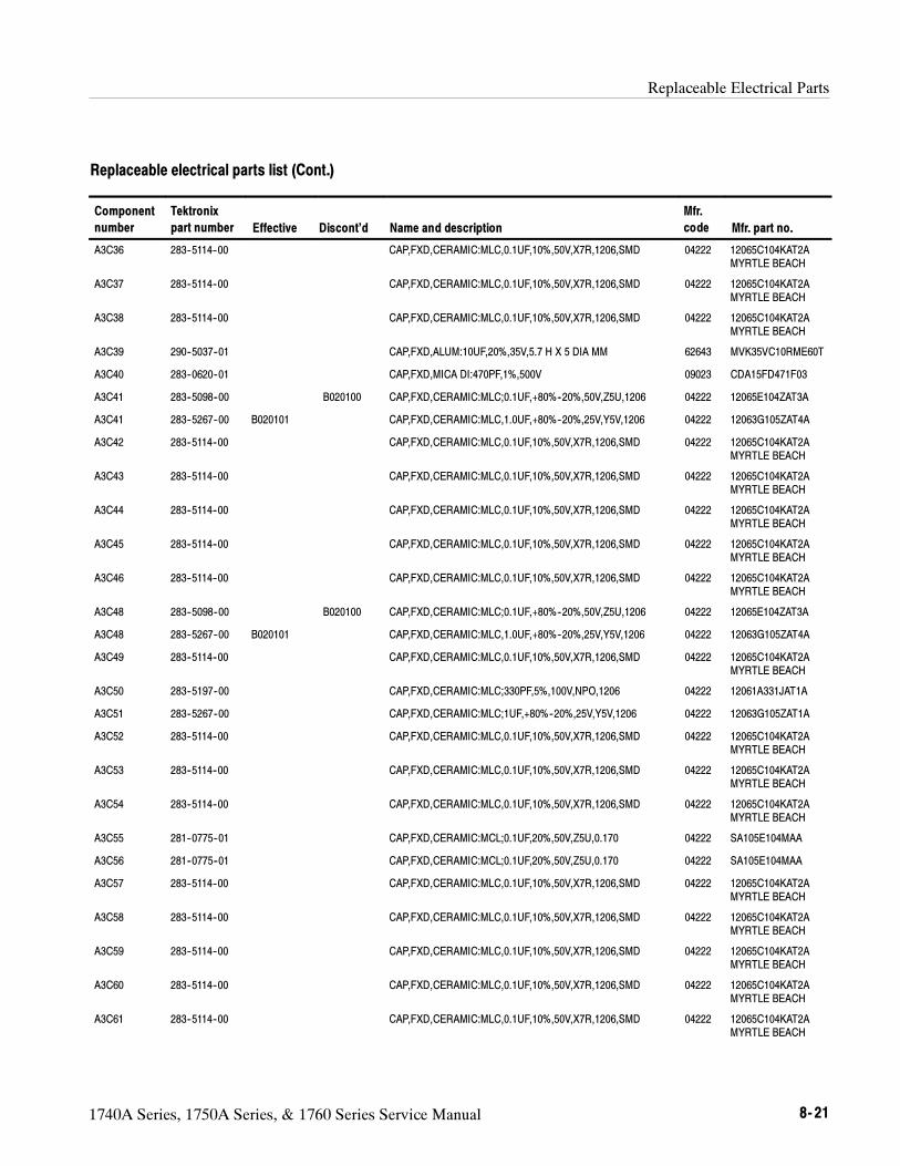
Replaceable Electrical Parts
1740A Series, 1750A Series, & 1760 Series Service Manual 8- 21
Replaceable electrical parts list (Cont.)
Component
number Mfr. part no.
Mfr.
codeName and descriptionDiscont’dEffective
Tektronix
part number
A3C36 283--5114--00 CAP,FXD,CERAMIC:MLC,0.1UF,10%,50V,X7R,1206,SMD 04222 12065C104KAT2AMYRTLE BEACH
A3C37 283--5114--00 CAP,FXD,CERAMIC:MLC,0.1UF,10%,50V,X7R,1206,SMD 04222 12065C104KAT2AMYRTLE BEACH
A3C38 283--5114--00 CAP,FXD,CERAMIC:MLC,0.1UF,10%,50V,X7R,1206,SMD 04222 12065C104KAT2AMYRTLE BEACH
A3C39 290--5037--01 CAP,FXD,ALUM:10UF,20%,35V,5.7 H X 5 DIA MM 62643 MVK35VC10RME60T
A3C40 283--0620--01 CAP,FXD,MICA DI:470PF,1%,500V 09023 CDA15FD471F03
A3C41 283--5098--00 B020100 CAP,FXD,CERAMIC:MLC;0.1UF,+80%--20%,50V,Z5U,1206 04222 12065E104ZAT3A
A3C41 283--5267--00 B020101 CAP,FXD,CERAMIC:MLC,1.0UF,+80%--20%,25V,Y5V,1206 04222 12063G105ZAT4A
A3C42 283--5114--00 CAP,FXD,CERAMIC:MLC,0.1UF,10%,50V,X7R,1206,SMD 04222 12065C104KAT2AMYRTLE BEACH
A3C43 283--5114--00 CAP,FXD,CERAMIC:MLC,0.1UF,10%,50V,X7R,1206,SMD 04222 12065C104KAT2AMYRTLE BEACH
A3C44 283--5114--00 CAP,FXD,CERAMIC:MLC,0.1UF,10%,50V,X7R,1206,SMD 04222 12065C104KAT2AMYRTLE BEACH
A3C45 283--5114--00 CAP,FXD,CERAMIC:MLC,0.1UF,10%,50V,X7R,1206,SMD 04222 12065C104KAT2AMYRTLE BEACH
A3C46 283--5114--00 CAP,FXD,CERAMIC:MLC,0.1UF,10%,50V,X7R,1206,SMD 04222 12065C104KAT2AMYRTLE BEACH
A3C48 283--5098--00 B020100 CAP,FXD,CERAMIC:MLC;0.1UF,+80%--20%,50V,Z5U,1206 04222 12065E104ZAT3A
A3C48 283--5267--00 B020101 CAP,FXD,CERAMIC:MLC,1.0UF,+80%--20%,25V,Y5V,1206 04222 12063G105ZAT4A
A3C49 283--5114--00 CAP,FXD,CERAMIC:MLC,0.1UF,10%,50V,X7R,1206,SMD 04222 12065C104KAT2AMYRTLE BEACH
A3C50 283--5197--00 CAP,FXD,CERAMIC:MLC;330PF,5%,100V,NPO,1206 04222 12061A331JAT1A
A3C51 283--5267--00 CAP,FXD,CERAMIC:MLC;1UF,+80%--20%,25V,Y5V,1206 04222 12063G105ZAT1A
A3C52 283--5114--00 CAP,FXD,CERAMIC:MLC,0.1UF,10%,50V,X7R,1206,SMD 04222 12065C104KAT2AMYRTLE BEACH
A3C53 283--5114--00 CAP,FXD,CERAMIC:MLC,0.1UF,10%,50V,X7R,1206,SMD 04222 12065C104KAT2AMYRTLE BEACH
A3C54 283--5114--00 CAP,FXD,CERAMIC:MLC,0.1UF,10%,50V,X7R,1206,SMD 04222 12065C104KAT2AMYRTLE BEACH
A3C55 281--0775--01 CAP,FXD,CERAMIC:MCL;0.1UF,20%,50V,Z5U,0.170 04222 SA105E104MAA
A3C56 281--0775--01 CAP,FXD,CERAMIC:MCL;0.1UF,20%,50V,Z5U,0.170 04222 SA105E104MAA
A3C57 283--5114--00 CAP,FXD,CERAMIC:MLC,0.1UF,10%,50V,X7R,1206,SMD 04222 12065C104KAT2AMYRTLE BEACH
A3C58 283--5114--00 CAP,FXD,CERAMIC:MLC,0.1UF,10%,50V,X7R,1206,SMD 04222 12065C104KAT2AMYRTLE BEACH
A3C59 283--5114--00 CAP,FXD,CERAMIC:MLC,0.1UF,10%,50V,X7R,1206,SMD 04222 12065C104KAT2AMYRTLE BEACH
A3C60 283--5114--00 CAP,FXD,CERAMIC:MLC,0.1UF,10%,50V,X7R,1206,SMD 04222 12065C104KAT2AMYRTLE BEACH
A3C61 283--5114--00 CAP,FXD,CERAMIC:MLC,0.1UF,10%,50V,X7R,1206,SMD 04222 12065C104KAT2AMYRTLE BEACH

Replaceable Electrical Parts
8- 22 1740A Series, 1750A Series, & 1760 Series Service Manual
Replaceable electrical parts list (Cont.)
Component
number Mfr. part no.
Mfr.
codeName and descriptionDiscont’dEffective
Tektronix
part number
A3C62 283--5114--00 CAP,FXD,CERAMIC:MLC,0.1UF,10%,50V,X7R,1206,SMD 04222 12065C104KAT2AMYRTLE BEACH
A3C63 283--5114--00 CAP,FXD,CERAMIC:MLC,0.1UF,10%,50V,X7R,1206,SMD 04222 12065C104KAT2AMYRTLE BEACH
A3C64 283--5114--00 CAP,FXD,CERAMIC:MLC,0.1UF,10%,50V,X7R,1206,SMD 04222 12065C104KAT2AMYRTLE BEACH
A3C65 283--5114--00 CAP,FXD,CERAMIC:MLC,0.1UF,10%,50V,X7R,1206,SMD 04222 12065C104KAT2AMYRTLE BEACH
A3C66 283--5114--00 CAP,FXD,CERAMIC:MLC,0.1UF,10%,50V,X7R,1206,SMD 04222 12065C104KAT2AMYRTLE BEACH
A3C67 283--5114--00 CAP,FXD,CERAMIC:MLC,0.1UF,10%,50V,X7R,1206,SMD 04222 12065C104KAT2AMYRTLE BEACH
A3C68 283--5203--00 CAP,FXD,CERAMIC:MLC;1000PF,10%,100V,X7R,1206 04222 12061C102KAT1A
A3C69 283--5114--00 CAP,FXD,CERAMIC:MLC,0.1UF,10%,50V,X7R,1206,SMD 04222 12065C104KAT2AMYRTLE BEACH
A3C70 283--5203--00 CAP,FXD,CERAMIC:MLC;1000PF,10%,100V,X7R,1206 04222 12061C102KAT1A
A3C71 283--5114--00 CAP,FXD,CERAMIC:MLC,0.1UF,10%,50V,X7R,1206,SMD 04222 12065C104KAT2AMYRTLE BEACH
A3C72 283--5114--00 CAP,FXD,CERAMIC:MLC,0.1UF,10%,50V,X7R,1206,SMD 04222 12065C104KAT2AMYRTLE BEACH
A3C73 283--5256--00 CAP,FXD:CERAMIC,MLC;0.1UF,CONTROL +/--10%,200V,
0.180 X 0.250 X7R
04222 18252C104KATRA
A3C74 283--5114--00 CAP,FXD,CERAMIC:MLC,0.1UF,10%,50V,X7R,1206,SMD 04222 12065C104KAT2AMYRTLE BEACH
A3C75 290--5037--01 CAP,FXD,ALUM:10UF,20%,35V,5.7 H X 5 DIA MM 62643 MVK35VC10RME60T
A3C76 283--5114--00 CAP,FXD,CERAMIC:MLC,0.1UF,10%,50V,X7R,1206,SMD 04222 12065C104KAT2AMYRTLE BEACH
A3C77 283--5114--00 CAP,FXD,CERAMIC:MLC,0.1UF,10%,50V,X7R,1206,SMD 04222 12065C104KAT2AMYRTLE BEACH
A3C78 283--5314--00 CAP,FXD,CERAMIC:MLC;0.7PF,+/--0.1PF,100V,+20 80009 283--5314--00
A3C79 283--5114--00 CAP,FXD,CERAMIC:MLC,0.1UF,10%,50V,X7R,1206,SMD 04222 12065C104KAT2AMYRTLE BEACH
A3C80 283--5114--00 CAP,FXD,CERAMIC:MLC,0.1UF,10%,50V,X7R,1206,SMD 04222 12065C104KAT2AMYRTLE BEACH
A3C81 283--5114--00 CAP,FXD,CERAMIC:MLC,0.1UF,10%,50V,X7R,1206,SMD 04222 12065C104KAT2AMYRTLE BEACH
A3C82 283--5068--00 CAP,FXD,CERAMIC:MLC;2200PF,10%,50V,X7R,1206 04222 12065C222KAT1A
A3C83 283--5001--00 B020100 CAP,FXD,CERAMIC:MLC;100PF,5%,50V,NPO,1206 TK2058 C3216C0G1H101J--
A3C83 283--5188--00 B020101 CAP,FXD,CERAMIC:MLC,100PF,5%,100V,NPO,SMD 04222 12061A101JAT2A
A3C84 283--5001--00 B020100 CAP,FXD,CERAMIC:MLC;100PF,5%,50V,NPO,1206 TK2058 C3216C0G1H101J--
A3C84 283--5188--00 B020101 CAP,FXD,CERAMIC:MLC,100PF,5%,100V,NPO,SMD 04222 12061A101JAT2A
A3C85 283--5114--00 CAP,FXD,CERAMIC:MLC,0.1UF,10%,50V,X7R,1206,SMD 04222 12065C104KAT2AMYRTLE BEACH
A3C86 283--5114--00 CAP,FXD,CERAMIC:MLC,0.1UF,10%,50V,X7R,1206,SMD 04222 12065C104KAT2AMYRTLE BEACH

Replaceable Electrical Parts
1740A Series, 1750A Series, & 1760 Series Service Manual 8- 23
Replaceable electrical parts list (Cont.)
Component
number Mfr. part no.
Mfr.
codeName and descriptionDiscont’dEffective
Tektronix
part number
A3C87 283--5267--00 CAP,FXD,CERAMIC:MLC;1UF,+80%--20%,25V,Y5V,1206 04222 12063G105ZAT1A
A3C88 283--5259--00 CAP,FXD,CERAMIC:MLC;6.8PF,+/--0.25PF,100V,NPO 04222 12061A6R8CAT1A
A3C89 283--5114--00 CAP,FXD,CERAMIC:MLC,0.1UF,10%,50V,X7R,1206,SMD 04222 12065C104KAT2AMYRTLE BEACH
A3C90 283--5114--00 CAP,FXD,CERAMIC:MLC,0.1UF,10%,50V,X7R,1206,SMD 04222 12065C104KAT2AMYRTLE BEACH
A3C91 281--0271--00 CAP,VAR,CER DI:7--50PF,50V 51406 TZBX4R500BA110T
A3C92 283--5188--00 B020101 CAP,FXD,CERAMIC:MLC,100PF,5%,100V,NPO,SMD 04222 12061A101JAT2A
A3C93 283--5259--00 CAP,FXD,CERAMIC:MLC;6.8PF,+/--0.25PF,100V,NPO 04222 12061A6R8CAT1A
A3C94 283--5314--00 CAP,FXD,CERAMIC:MLC;0.7PF,+/--0.1PF,100V,+20 80009 283--5314--00
A3C95 283--5114--00 CAP,FXD,CERAMIC:MLC,0.1UF,10%,50V,X7R,1206,SMD 04222 12065C104KAT2AMYRTLE BEACH
A3C96 283--5114--00 CAP,FXD,CERAMIC:MLC,0.1UF,10%,50V,X7R,1206,SMD 04222 12065C104KAT2AMYRTLE BEACH
A3C97 283--5114--00 CAP,FXD,CERAMIC:MLC,0.1UF,10%,50V,X7R,1206,SMD 04222 12065C104KAT2AMYRTLE BEACH
A3C98 283--5188--00 B020101 CAP,FXD,CERAMIC:MLC,100PF,5%,100V,NPO,SMD 04222 12061A101JAT2A
A3C99 283--5114--00 CAP,FXD,CERAMIC:MLC,0.1UF,10%,50V,X7R,1206,SMD 04222 12065C104KAT2AMYRTLE BEACH
A3C100 283--5114--00 CAP,FXD,CERAMIC:MLC,0.1UF,10%,50V,X7R,1206,SMD 04222 12065C104KAT2AMYRTLE BEACH
A3C101 285--1349--00 CAP,FXD,MTLZD:0.1UF,5%,63VDC TK1913 MKS2 .1/63/5
A3C102 283--5114--00 CAP,FXD,CERAMIC:MLC,0.1UF,10%,50V,X7R,1206,SMD 04222 12065C104KAT2AMYRTLE BEACH
A3C103 290--5037--01 CAP,FXD,ALUM:10UF,20%,35V,5.7 H X 5 DIA MM 62643 MVK35VC10RME60T
A3C104 283--5114--00 CAP,FXD,CERAMIC:MLC,0.1UF,10%,50V,X7R,1206,SMD 04222 12065C104KAT2AMYRTLE BEACH
A3C105 283--0934--00 CAP,FXD,PLSTC:0.0022UF,5%,100WVDC TK1913 FKP2 2200/100/5
A3C106 283--5114--00 CAP,FXD,CERAMIC:MLC,0.1UF,10%,50V,X7R,1206,SMD 04222 12065C104KAT2AMYRTLE BEACH
A3C107 283--5114--00 CAP,FXD,CERAMIC:MLC,0.1UF,10%,50V,X7R,1206,SMD 04222 12065C104KAT2AMYRTLE BEACH
A3C108 283--5114--00 CAP,FXD,CERAMIC:MLC,0.1UF,10%,50V,X7R,1206,SMD 04222 12065C104KAT2AMYRTLE BEACH
A3C110 283--5114--00 CAP,FXD,CERAMIC:MLC,0.1UF,10%,50V,X7R,1206,SMD 04222 12065C104KAT2AMYRTLE BEACH
A3C111 283--5189--00 CAP,FXD,CERAMIC:MLC;220PF,5%,100V,NPO,1206 04222 12061A221JAT1A
A3C112 283--5114--00 CAP,FXD,CERAMIC:MLC,0.1UF,10%,50V,X7R,1206,SMD 04222 12065C104KAT2AMYRTLE BEACH
A3C113 283--5114--00 CAP,FXD,CERAMIC:MLC,0.1UF,10%,50V,X7R,1206,SMD 04222 12065C104KAT2AMYRTLE BEACH
A3C115 283--5114--00 CAP,FXD,CERAMIC:MLC,0.1UF,10%,50V,X7R,1206,SMD 04222 12065C104KAT2AMYRTLE BEACH

Replaceable Electrical Parts
8- 24 1740A Series, 1750A Series, & 1760 Series Service Manual
Replaceable electrical parts list (Cont.)
Component
number Mfr. part no.
Mfr.
codeName and descriptionDiscont’dEffective
Tektronix
part number
A3C116 283--5114--00 CAP,FXD,CERAMIC:MLC,0.1UF,10%,50V,X7R,1206,SMD 04222 12065C104KAT2AMYRTLE BEACH
A3C117 283--5188--00 B020101 CAP,FXD,CERAMIC:MLC,100PF,5%,100V,NPO,SMD 04222 12061A101JAT2A
A3C118 283--5188--00 B020101 CAP,FXD,CERAMIC:MLC,100PF,5%,100V,NPO,SMD 04222 12061A101JAT2A
A3C119 283--5114--00 CAP,FXD,CERAMIC:MLC,0.1UF,10%,50V,X7R,1206,SMD 04222 12065C104KAT2AMYRTLE BEACH
A3C120 283--5267--00 CAP,FXD,CERAMIC:MLC;1UF,+80%--20%,25V,Y5V,1206 04222 12063G105ZAT1A
A3C121 283--5114--00 CAP,FXD,CERAMIC:MLC,0.1UF,10%,50V,X7R,1206,SMD 04222 12065C104KAT2AMYRTLE BEACH
A3C122 283--5114--00 CAP,FXD,CERAMIC:MLC,0.1UF,10%,50V,X7R,1206,SMD 04222 12065C104KAT2AMYRTLE BEACH
A3C123 283--5114--00 CAP,FXD,CERAMIC:MLC,0.1UF,10%,50V,X7R,1206,SMD 04222 12065C104KAT2AMYRTLE BEACH
A3C124 283--5114--00 CAP,FXD,CERAMIC:MLC,0.1UF,10%,50V,X7R,1206,SMD 04222 12065C104KAT2AMYRTLE BEACH
A3C125 283--0698--01 CAP,FXD,MICA DI:390PF,1%,500V 09023 CDA15FD391F03
A3C126 283--5108--00 CAP,FXD,CERAMIC:MLC;68PF,5%,100V,NPO,1206 04222 12061A680JAT1A
A3C127 283--5114--00 CAP,FXD,CERAMIC:MLC,0.1UF,10%,50V,X7R,1206,SMD 04222 12065C104KAT2AMYRTLE BEACH
A3C128 283--5201--00 CAP,FXD,CERAMIC:MLC;33PF,5%,100V,NPO,1206 04222 12061A330JAT1A
A3C129 283--5195--00 CAP,FXD,CERAMIC:MLC;10PF,5%,100V ,NPO,1206 04222 12061A100JAT1A
A3C130 283--5107--00 CAP,FXD,CERAMIC:MLC;22PF,5%,100V,NPO,1206 04222 12061A220JAT1A
A3C131 281--5007--00 CAP,VAR,CERAMIC:4.5--20PF,100V,N750+/--300PPM/C,4 X 4.5
X 2.7MM
52769 GKG20066--##
A3C132 283--0640--01 CAP,FXD,MICA DI:160PF,1%,100V TK0891 ADVISE
A3C133 283--5188--00 B020101 CAP,FXD,CERAMIC:MLC,100PF,5%,100V,NPO,SMD 04222 12061A101JAT2A
A3C134 283--5108--00 CAP,FXD,CERAMIC:MLC;68PF,5%,100V,NPO,1206 04222 12061A680JAT1A
A3C135 281--0271--00 CAP,VAR,CER DI:7--50PF,50V 51406 TZBX4R500BA110T
A3C136 283--5114--00 CAP,FXD,CERAMIC:MLC,0.1UF,10%,50V,X7R,1206,SMD 04222 12065C104KAT2AMYRTLE BEACH
A3C138 283--5003--00 CAP,FXD,CERAMIC:MLC;0.01UF,10%,50V,X7R,1206 TK2058 C3216X7R1H103K--
A3C139 290--5037--01 CAP,FXD,ALUM:10UF,20%,35V,5.7 H X 5 DIA MM 62643 MVK35VC10RME60T
A3C140 283--5267--00 CAP,FXD,CERAMIC:MLC;1UF,+80%--20%,25V,Y5V,1206 04222 12063G105ZAT1A
A3C141 283--5114--00 CAP,FXD,CERAMIC:MLC,0.1UF,10%,50V,X7R,1206,SMD 04222 12065C104KAT2AMYRTLE BEACH
A3C142 283--5114--00 CAP,FXD,CERAMIC:MLC,0.1UF,10%,50V,X7R,1206,SMD 04222 12065C104KAT2AMYRTLE BEACH
A3C143 283--5114--00 CAP,FXD,CERAMIC:MLC,0.1UF,10%,50V,X7R,1206,SMD 04222 12065C104KAT2AMYRTLE BEACH
A3C144 283--0639--01 CAP,FXD,MICA DI:56PF,1%,500V 09023 CDA15ED560F03
A3C145 283--5108--00 CAP,FXD,CERAMIC:MLC;68PF,5%,100V,NPO,1206 04222 12061A680JAT1A
A3C146 283--5196--00 CAP,FXD,CERAMIC:MLC;47PF,5%,100V,NPO,1206 04222 12061A470JAT1A
Replaceable Electrical Parts
1740A Series, 1750A Series, & 1760 Series Service Manual 8- 25
Replaceable electrical parts list (Cont.)
Component
number Mfr. part no.
Mfr.
codeName and descriptionDiscont’dEffective
Tektronix
part number
A3C147 283--5114--00 CAP,FXD,CERAMIC:MLC,0.1UF,10%,50V,X7R,1206,SMD 04222 12065C104KAT2AMYRTLE BEACH
A3C148 283--5114--00 CAP,FXD,CERAMIC:MLC,0.1UF,10%,50V,X7R,1206,SMD 04222 12065C104KAT2AMYRTLE BEACH
A3C149 283--5267--00 CAP,FXD,CERAMIC:MLC;1UF,+80%--20%,25V,Y5V,1206 04222 12063G105ZAT1A
A3C150 283--5114--00 CAP,FXD,CERAMIC:MLC,0.1UF,10%,50V,X7R,1206,SMD 04222 12065C104KAT2AMYRTLE BEACH
A3C151 281--0271--00 CAP,VAR,CER DI:7--50PF,50V 51406 TZBX4R500BA110T
A3C152 283--5188--00 B020101 CAP,FXD,CERAMIC:MLC,100PF,5%,100V,NPO,SMD 04222 12061A101JAT2A
A3C153 283--5114--00 CAP,FXD,CERAMIC:MLC,0.1UF,10%,50V,X7R,1206,SMD 04222 12065C104KAT2AMYRTLE BEACH
A3C154 283--5106--00 CAP,FXD,CERAMIC:MLC;470PF,5%,100V,NPO,1206 04222 12061A471JAT1A
A3C155 283--5197--00 B020101 CAP,FXD,CERAMIC:MLC,330PF,5%,100V,NPO,SMD 04222 12061A331JAT2A
A3C156 283--5114--00 CAP,FXD,CERAMIC:MLC,0.1UF,10%,50V,X7R,1206,SMD 04222 12065C104KAT2AMYRTLE BEACH
A3C157 283--5114--00 CAP,FXD,CERAMIC:MLC,0.1UF,10%,50V,X7R,1206,SMD 04222 12065C104KAT2AMYRTLE BEACH
A3C158 281--0271--00 CAP,VAR,CER DI:7--50PF,50V 51406 TZBX4R500BA110T
A3C159 283--5114--00 CAP,FXD,CERAMIC:MLC,0.1UF,10%,50V,X7R,1206,SMD 04222 12065C104KAT2AMYRTLE BEACH
A3C160 283--5106--00 CAP,FXD,CERAMIC:MLC;470PF,5%,100V,NPO,1206 04222 12061A471JAT1A
A3C161 283--5106--00 CAP,FXD,CERAMIC:MLC;470PF,5%,100V,NPO,1206 04222 12061A471JAT1A
A3C162 283--5267--00 B020101 CAP,FXD,CERAMIC:MLC,1.0UF,+80%--20%,25V,Y5V 04222 12063G105ZAT4A
A3C163 283--5114--00 CAP,FXD,CERAMIC:MLC,0.1UF,10%,50V,X7R,1206,SMD 04222 12065C104KAT2AMYRTLE BEACH
A3C164 283--5114--00 CAP,FXD,CERAMIC:MLC,0.1UF,10%,50V,X7R,1206,SMD 04222 12065C104KAT2AMYRTLE BEACH
A3C165 283--5189--00 CAP,FXD,CERAMIC:MLC;220PF,5%,100V,NPO,1206 04222 12061A221JAT1A
A3C166 283--5114--00 CAP,FXD,CERAMIC:MLC,0.1UF,10%,50V,X7R,1206,SMD 04222 12065C104KAT2AMYRTLE BEACH
A3C167 283--5197--00 B020101 CAP,FXD,CERAMIC:MLC,330PF,5%,100V,NPO,SMD 04222 12061A331JAT2A
A3C168 283--5114--00 CAP,FXD,CERAMIC:MLC,0.1UF,10%,50V,X7R,1206,SMD 04222 12065C104KAT2AMYRTLE BEACH
A3C169 283--5109--00 CAP,FXD,CERAMIC:MLC;680PF,5%,100V,NPO,1206 04222 12061A681JAT1A
A3C170 290--5036--01 671-2355-13 CAP,FXD,ALUM:22UF,20%,16V,5.7MM(0.224) 62643 MVK16VC22RME60T
A3C170 283--5267--00 671-2355-14 CAP,FXD,CERAMIC:MLC,1.0UF,+80%--20%,25V,1206,SMD 04222 12063G105ZAT4A
A3C171 290--5036--01 671-2355-13 CAP,FXD,ALUM:22UF,20%,16V,5.7MM(0.224) 62643 MVK16VC22RME60T
A3C171 283--5267--00 671-2355-14 CAP,FXD,CERAMIC:MLC,1.0UF,+80%--20%,25V,1206,SMD 04222 12063G105ZAT4A
A3C172 290--5036--01 671-2355-13 CAP,FXD,ALUM:22UF,20%,16V,5.7MM(0.224) 62643 MVK16VC22RME60T
A3C172 283--5267--00 671-2355-14 CAP,FXD,CERAMIC:MLC,1.0UF,+80%--20%,25V,1206,SMD 04222 12063G105ZAT4A
A3C173 283--5114--00 CAP,FXD,CERAMIC:MLC,0.1UF,10%,50V,X7R,1206,SMD 04222 12065C104KAT2AMYRTLE BEACH

Replaceable Electrical Parts
8- 26 1740A Series, 1750A Series, & 1760 Series Service Manual
Replaceable electrical parts list (Cont.)
Component
number Mfr. part no.
Mfr.
codeName and descriptionDiscont’dEffective
Tektronix
part number
A3C174 283--5114--00 CAP,FXD,CERAMIC:MLC,0.1UF,10%,50V,X7R,1206,SMD 04222 12065C104KAT2AMYRTLE BEACH
A3C175 290--5036--01 671-2355-13 CAP,FXD,ALUM:22UF,20%,16V,5.7MM(0.224) 62643 MVK16VC22RME60T
A3C175 283--5267--00 671-2355-14 CAP,FXD,CERAMIC:MLC,1.0UF,+80%--20%,25V1206,SMD 04222 12063G105ZAT4A
A3C176 283--5188--00 B020101 CAP,FXD,CERAMIC:MLC,100PF,5%,100V,NPO,SMD 04222 12061A101JAT2A
A3C177 283--5114--00 CAP,FXD,CERAMIC:MLC,0.1UF,10%,50V,X7R,1206,SMD 04222 12065C104KAT2AMYRTLE BEACH
A3C178 283--5188--00 B020101 CAP,FXD,CERAMIC:MLC,100PF,5%,100V,NPO,SMD 04222 12061A101JAT2A
A3C179 283--5267--00 CAP,FXD,CERAMIC:MLC;1UF,+80%--20%,25V,Y5V,1206 04222 12063G105ZAT1A
A3C180 283--5267--00 CAP,FXD,CERAMIC:MLC;1UF,+80%--20%,25V,Y5V,1206 04222 12063G105ZAT1A
A3C181 283--5197--00 B020101 CAP,FXD,CERAMIC:MLC,330PF,5%,100V,NPO,SMD 04222 12061A331JAT2A
A3C182 283--5114--00 CAP,FXD,CERAMIC:MLC,0.1UF,10%,50V,X7R,1206,SMD 04222 12065C104KAT2AMYRTLE BEACH
A3C190 283--5248--00 CAP,FXD,CERAMIC:MLC;82 PF,5%,200V,NPO;1206 95275 VJ1206Q820J--NCAT
A3C191 283--5267--00 B020101 CAP,FXD,CERAMIC:MLC,1.0UF,+80%--20%,25V,Y5V 04222 12063G105ZAT4A
A3C192 283--5267--00 B020101 CAP,FXD,CERAMIC:MLC,1.0UF,+80%--20%,25V,Y5V,1206 04222 12063G105ZAT4A
A3C221 283--5106--00 B020101 CAP,FXD,CERAMIC:MLC,470PF,5%,100V,NPO,SMD 04222 12061A471JAT2A
A3J1 131--3718--00 CONN,HDR:PCB;MALE,STR,2 X 5,0.1 CTR,0.385H X 0.120
TAIL,SHRD/4 SIDES,CTR PLZ,30 GOLD,0.150 END DIM
TK1462 FAP--10--08--4--OAS
A3J2 131--3323--00 CONN,HDR:PCB;MALE,STR,2 X 20,0.1 CTR,0.365D 22526 66506--025
A3J3 131--4752--00 CONN,HDR::PCB;MALE,45 DEG,1 X 2,0.1CTR,0.240 MLG X
0.110 TAIL,30 GOLD
58050 082--0243--AS10
A3J4 131--4530--00 CONN,HDR:PCB;MALE,STR,1 X 3,0.1 CTR,0.230
MLG X 0.120 TAIL,30GOLD,BD RETENTION
00779 104344--1
A3J5 131--3323--00 CONN,HDR:PCB;MALE,STR,2 X 20,0.1 CTR,0.365D 22526 66506--025
A3J6 175--9797--00 CA ASSY,SP:FLAT FLEX;FLX,10,27 AWG,2.5 L,1X10,BOX X
STR,SLDR TAB,CONN NON PLZ
TK2469 175--9797--00
A3J9 131--3364--00 CONN,HDR:PCB;MALE,STR,2 X 17,0.1 CTR,0.365D 53387 2534--6002UB
A3J12 131--3181--00 CONN,HDR:PCB;MALE,RTANG,2 X 20,0.1CTR,0.330 H X 0.112
TAIL,SHRD/4 SIDES,CTR PLZ,30 GOLD,0.390 MLG,HIGH
TEMP
22526 69155--440R
A3J13 131--3323--00 CONN,HDR:PCB;MALE,STR,2 X 20,0.1 CTR,0.365D 22526 66506--025
A3J14 174--2743--00 CA ASSY SP:RIBBON;IDC,34,28 AWG,2X17,0.1 CTR,PCB X 25
POS,DSUB,THD INSERTS,1.2 L & 9POS,DSUB,FEMALE,
THD INSERTS,2.2 L
53387 174--2743--00
A3L1 108--5018--00 INDUCTOR,FXD:POWER;4.7UH,20%,I<0.315 A,RDC<
1 OHM,Q>50,SRF>45 MHZ
TK2058 NL453232T--4R7M
A3L2 108--5018--00 INDUCTOR,FXD:POWER;4.7UH,20%,I<0.315 A,RDC<
1 OHM,Q>50,SRF>45 MHZ
TK2058 NL453232T--4R7M
A3L3 108--5002--00 INDUCTOR,FXD:SIGNAL;15UH,10%,I<0.2A,RDC<2.5
OHM,Q>50,SRF>20MHZ
TK2058 NL453232T--150K
A3L4 108--5002--00 INDUCTOR,FXD:SIGNAL;15UH,10%,I<0.2A,RDC<2.5
OHM,Q>50,SRF>20MHZ
TK2058 NL453232T--150K

Replaceable Electrical Parts
1740A Series, 1750A Series, & 1760 Series Service Manual 8- 27
Replaceable electrical parts list (Cont.)
Component
number Mfr. part no.
Mfr.
codeName and descriptionDiscont’dEffective
Tektronix
part number
A3L5 114--0482--00 INDUCTOR,VAR:SHIELDED;32--48UH,Q>32@L=40UH,E 02113 SLOT TEN--04--11
A3L6 114--0482--00 INDUCTOR,VAR:SHIELDED;32--48UH,Q>32@L=40UH,E 02113 SLOT TEN--04--11
A3L7 108--5002--00 INDUCTOR,FXD:SIGNAL;15UH,10%,I<0.2A,RDC<2.5
OHM,Q>50,SRF>20MHZ
TK2058 NL453232T--150K
A3L8 108--5002--00 INDUCTOR,FXD:SIGNAL;15UH,10%,I<0.2A,RDC<2.5
OHM,Q>50,SRF>20MHZ
TK2058 NL453232T--150K
A3L9 108--5018--00 INDUCTOR,FXD:POWER;4.7UH,20%,I<0.315 A,RDC<
1 OHM,Q>50,SRF>45 MHZ
TK2058 NL453232T--4R7M
A3P4 131--3199--00 CONN,SHUNT:SHUNT;FEMALE,STR,1 X 2,0.1 CTR,
0.2 H,LOW PROFILE,JUMPER
22526 68786--202
A3Q1 151--5021--00 XTR,SIG:BIPOLAR,NPN;40V,600MA,300MHZ,AMPL 04713 MMBT2222ALT1
A3Q2 151--5021--00 XTR,SIG:BIPOLAR,NPN;40V,600MA,300MHZ,AMPL 04713 MMBT2222ALT1
A3Q3 151--5001--00 XTR,SIG:BIPOLAR,NPN;40V,200MA,300MHZ,AMPL 0LUA3 PMBT3904TRL
A3Q4 151--5000--00 XTR,SIG:BIPOLAR,PNP;40V,200MA,250MHZ,AMPL 0LUA3 PMBT3906TRL
A3Q5 151--5000--00 XTR,SIG:BIPOLAR,PNP;40V,200MA,250MHZ,AMPL 0LUA3 PMBT3906TRL
A3Q6 151--5001--00 XTR,SIG:BIPOLAR,NPN;40V,200MA,300MHZ,AMPL 0LUA3 PMBT3904TRL
A3Q7 151--5001--00 XTR,SIG:BIPOLAR,NPN;40V,200MA,300MHZ,AMPL 0LUA3 PMBT3904TRL
A3Q8 151--0350--03 XTR,SIG:BIPOLAR,PNP;150V,600MA,100MHZ,AMPL 04713 2N5401RLRP
A3Q9 151--5035--00 B020101 XTR,SIG:BIPOLAR,NPN,25V,30MA,650MHZ,AMPL 1MQ07 MMBTH10LT1
A3Q10 151--0211--00 XTR,SIG:BIPOLAR,NPN;30V VCEO,55V VCBO,400MA,
500MHZ,AMPL
04713 2N3866
*ATTACHED PARTS*
214--2593--00 HEAT SINK,SEMIC:XTR/IC,TO--5/TO--39;PRESS--ON,0.5”
DIA,ALUMINUM,BLACK ANODIZE
13103 2257B
*END ATTACHED PARTS*
A3Q11 151--0347--02 XTR,SIG:BIPOLAR,NPN;160V,600MA,100MHZ,AMPL 04713 2N5551RLRP
A3Q12 151--5000--00 XTR,SIG:BIPOLAR,PNP;40V,200MA,250MHZ,AMPL 0LUA3 PMBT3906TRL
A3Q13 151--0347--02 XTR,SIG:BIPOLAR,NPN;160V,600MA,100MHZ,AMPL 04713 2N5551RLRP
A3Q14 151--5000--00 XTR,SIG:BIPOLAR,PNP;40V,200MA,250MHZ,AMPL 0LUA3 PMBT3906TRL
A3Q15 151--0350--03 XTR,SIG:BIPOLAR,PNP;150V,600MA,100MHZ,AMPL 04713 2N5401RLRP
A3Q16 151--0211--00 XTR,SIG:BIPOLAR,NPN;30V VCEO,55V VCBO,400MA,
500MHZ,AMPL
04713 2N3866
*ATTACHED PARTS*
214--2593--00 HEAT SINK,SEMIC:XTR/IC,TO--5/TO--39;PRESS--ON,0.5”
DIA,ALUMINUM,BLACK ANODIZE
13103 2257B
*END ATTACHED PARTS*
A3Q17 151--5001--00 XTR,SIG:BIPOLAR,NPN;40V,200MA,300MHZ,AMPL 0LUA3 PMBT3904TRL
A3Q19 151--5000--00 XTR,SIG:BIPOLAR,PNP;40V,200MA,250MHZ,AMPL 0LUA3 PMBT3906TRL
A3Q20 151--5029--00 XTR,SIG:BIPOLAR,NPN;15V,500MA,SWITCHING 04713 MMBT2369LT1
A3Q21 151--5001--00 XTR,SIG:BIPOLAR,NPN;40V,200MA,300MHZ,AMPL 0LUA3 PMBT3904TRL
A3Q22 151--5000--00 XTR,SIG:BIPOLAR,PNP;40V,200MA,250MHZ,AMPL 0LUA3 PMBT3906TRL
Replaceable Electrical Parts
8- 28 1740A Series, 1750A Series, & 1760 Series Service Manual
Replaceable electrical parts list (Cont.)
Component
number Mfr. part no.
Mfr.
codeName and descriptionDiscont’dEffective
Tektronix
part number
A3Q23 151--5000--00 XTR,SIG:BIPOLAR,PNP;40V,200MA,250MHZ,AMPL 0LUA3 PMBT3906TRL
A3Q24 151--5000--00 XTR,SIG:BIPOLAR,PNP;40V,200MA,250MHZ,AMPL 0LUA3 PMBT3906TRL
A3Q25 151--5001--00 XTR,SIG:BIPOLAR,NPN;40V,200MA,300MHZ,AMPL 0LUA3 PMBT3904TRL
A3Q26 151--5001--00 XTR,SIG:BIPOLAR,NPN;40V,200MA,300MHZ,AMPL 0LUA3 PMBT3904TRL
A3Q27 151--5001--00 XTR,SIG:BIPOLAR,NPN;40V,200MA,300MHZ,AMPL 0LUA3 PMBT3904TRL
A3Q28 151--5002--00 XTR,SIG:JFET,N--CH;5V,75MA,60 OHM,SWITCH 04713 MMBF4392LT1
A3Q29 151--5001--00 XTR,SIG:BIPOLAR,NPN;40V,200MA,300MHZ,AMPL 0LUA3 PMBT3904TRL
A3R1 321--5042--00 RES,FXD:THICK FILM;39.2 OHM,1%,0.125W,TC=100 PPM 57668 MCR18FWEA39E2
A3R2 321--5042--00 RES,FXD:THICK FILM;39.2 OHM,1%,0.125W,TC=100 PPM 57668 MCR18FWEA39E2
A3R3 321--5042--00 RES,FXD:THICK FILM;39.2 OHM,1%,0.125W,TC=100 PPM 57668 MCR18FWEA39E2
A3R4 321--5042--00 RES,FXD:THICK FILM;39.2 OHM,1%,0.125W,TC=100 PPM 57668 MCR18FWEA39E2
A3R5 321--5018--00 RES,FXD:THICK FILM;1.0K OHM,1%,0.125W,TC=100 PPM 50139 BCK1001FT
A3R6 311--2442--02 RES,VAR,PNL:CP;10K OHM,10%,0.5W,LINEAR,CONTINIOUS
ROTATION,0.5 SQ,2.0 LONG SHAFT
12697 S--1--20629
A3R7 311--2442--02 RES,VAR,PNL:CP;10K OHM,10%,0.5W,LINEAR,CONTINIOUS
ROTATION,0.5 SQ,2.0 LONG SHAFT
12697 S--1--20629
A3R8 311--2442--02 RES,VAR,PNL:CP;10K OHM,10%,0.5W,LINEAR,CONTINIOUS
ROTATION,0.5 SQ,2.0 LONG SHAFT
12697 S--1--20629
A3R9 311--2442--02 RES,VAR,PNL:CP;10K OHM,10%,0.5W,LINEAR,CONTINIOUS
ROTATION,0.5 SQ,2.0 LONG SHAFT
12697 S--1--20629
A3R10 311--2442--02 RES,VAR,PNL:CP;10K OHM,10%,0.5W,LINEAR,CONTINIOUS
ROTATION,0.5 SQ,2.0 LONG SHAFT
12697 S--1--20629
A3R11 321--5024--00 RES,FXD:THICK FILM;3.32K OHM,1%,0.125W,TC=100 PPM 50139 BCK3321FT
A3R12 321--5018--00 RES,FXD:THICK FILM;1.0K OHM,1%,0.125W,TC=100 PPM 50139 BCK1001FT
A3R13 321--5024--00 RES,FXD:THICK FILM;3.32K OHM,1%,0.125W,TC=100 PPM 50139 BCK3321FT
A3R14 321--5030--00 RES,FXD:THICK FILM;10.0K OHM,1%,0.125W,TC=100 PPM 50139 BCK1002FT
A3R15 321--5047--00 RES,FXD:THICK FILM;100K OHM,1%,0.125W,TC=100 PPM 50139 BCK1003FT
A3R16 321--5034--00 RES,FXD:THICK FILM;22.1K OHM,1%,0.125W,TC=100 PPM 50139 BCK2212FT
A3R17 321--5034--00 RES,FXD:THICK FILM;22.1K OHM,1%,0.125W,TC=100 PPM 50139 BCK2212FT
A3R18 321--5034--00 RES,FXD:THICK FILM;22.1K OHM,1%,0.125W,TC=100 PPM 50139 BCK2212FT
A3R19 321--5000--00 RES,FXD:THICK FILM;10 OHM,1%,0.125W,TC=100 PPM 59124 RK73H2B10R0FT
A3R20 321--5020--00 RES,FXD:THICK FILM;1.5K OHM,1%,0.125W,TC=100 PPM 50139 BCK1501FT
A3R21 307--5041--00 RES NTWK,FXD,FI:4.7K OHM,2%,0.125W 57924 4816P--002--472
A3R22 321--5042--00 RES,FXD:THICK FILM;39.2 OHM,1%,0.125W,TC=100 PPM 57668 MCR18FWEA39E2
A3R23 321--5051--00 RES,FXD:THICK FILM;0 OHM,1%,0.125W,TC=100 PPM 09969 CRCW1206 JUMPER
A3R24 321--5030--00 RES,FXD:THICK FILM;10.0K OHM,1%,0.125W,TC=100 PPM 50139 BCK1002FT
A3R25 321--5051--00 RES,FXD:THICK FILM;0 OHM,1%,0.125W,TC=100 PPM 09969 CRCW1206 JUMPER
A3R26 321--5051--00 RES,FXD:THICK FILM;0 OHM,1%,0.125W,TC=100 PPM 09969 CRCW1206 JUMPER

Replaceable Electrical Parts
1740A Series, 1750A Series, & 1760 Series Service Manual 8- 29
Replaceable electrical parts list (Cont.)
Component
number Mfr. part no.
Mfr.
codeName and descriptionDiscont’dEffective
Tektronix
part number
A3R27 321--5051--00 RES,FXD:THICK FILM;0 OHM,1%,0.125W,TC=100 PPM 09969 CRCW1206 JUMPER
A3R28 307--5041--00 RES NTWK,FXD,FI:4.7K OHM,2%,0.125W 57924 4816P--002--472
A3R29 321--5018--00 RES,FXD:THICK FILM;1.0K OHM,1%,0.125W,TC=100 PPM 50139 BCK1001FT
A3R30 321--5026--00 RES,FXD:THICK FILM;4.75K OHM,1%,0.125W,TC=100 PPM 50139 BCK4751FT
A3R31 321--5026--00 RES,FXD:THICK FILM;4.75K OHM,1%,0.125W,TC=100 PPM 50139 BCK4751FT
A3R32 321--5208--00 RES,FXD:THICK FILM;10M OHM,5%,0.125W,TC=100 59124 RK73H2B1005FT
A3R33 321--5048--00 RES,FXD:THICK FILM;332K OHM,1%,0.125W,TC=100 PPM 57668 MCR18FXEA332K
A3R34 321--5026--00 RES,FXD:THICK FILM;4.75K OHM,1%,0.125W,TC=100 PPM 50139 BCK4751FT
A3R35 321--5026--00 RES,FXD:THICK FILM;4.75K OHM,1%,0.125W,TC=100 PPM 50139 BCK4751FT
A3R36 321--5026--00 RES,FXD:THICK FILM;4.75K OHM,1%,0.125W,TC=100 PPM 50139 BCK4751FT
A3R37 321--5026--00 RES,FXD:THICK FILM;4.75K OHM,1%,0.125W,TC=100 PPM 50139 BCK4751FT
A3R38 321--5026--00 RES,FXD:THICK FILM;4.75K OHM,1%,0.125W,TC=100 PPM 50139 BCK4751FT
A3R39 321--5026--00 RES,FXD:THICK FILM;4.75K OHM,1%,0.125W,TC=100 PPM 50139 BCK4751FT
A3R40 321--5030--00 RES,FXD:THICK FILM;10.0K OHM,1%,0.125W,TC=100 PPM 50139 BCK1002FT
A3R41 321--5030--00 RES,FXD:THICK FILM;10.0K OHM,1%,0.125W,TC=100 PPM 50139 BCK1002FT
A3R42 321--5026--00 RES,FXD:THICK FILM;4.75K OHM,1%,0.125W,TC=100 PPM 50139 BCK4751FT
A3R43 321--5030--00 RES,FXD:THICK FILM;10.0K OHM,1%,0.125W,TC=100 PPM 50139 BCK1002FT
A3R44 321--5012--00 RES,FXD:THICK FILM;332 OHM,1%,0.125W,TC=100 50139 BCK3320FT
A3R45 321--5042--00 RES,FXD:THICK FILM;39.2 OHM,1%,0.125W,TC=100 PPM 57668 MCR18FWEA39E2
A3R46 321--5090--00 RES,FXD:THICK FILM; 20K OHM,0.125W,100 PPM,1206,T&R 50139 BCK2002FT
A3R47 321--5022--00 RES,FXD:THICK FILM;2.21K OHM,1%,0.125W,TC=100 PPM 50139 BCK2211FT
A3R48 321--5030--00 RES,FXD:THICK FILM;10.0K OHM,1%,0.125W,TC=100 PPM 50139 BCK1002FT
A3R49 321--5030--00 RES,FXD:THICK FILM;10.0K OHM,1%,0.125W,TC=100 PPM 50139 BCK1002FT
A3R50 321--5030--00 RES,FXD:THICK FILM;10.0K OHM,1%,0.125W,TC=100 PPM 50139 BCK1002FT
A3R51 321--5030--00 RES,FXD:THICK FILM;10.0K OHM,1%,0.125W,TC=100 PPM 50139 BCK1002FT
A3R52 321--5030--00 RES,FXD:THICK FILM;10.0K OHM,1%,0.125W,TC=100 PPM 50139 BCK1002FT
A3R53 321--5169--00 RES,FXD:THICK FILM;475K OHM,1%,0.125W,TC=100 PPM 59124 RK73H2B4753FT
A3R54 321--5035--00 RES,FXD:THICK FILM;27.4K OHM,1%,0.125W,TC=100 PPM 50139 BCK2742FT
A3R55 321--5030--00 RES,FXD:THICK FILM;10.0K OHM,1%,0.125W,TC=100 PPM 50139 BCK1002FT
A3R56 321--5042--00 RES,FXD:THICK FILM;39.2 OHM,1%,0.125W,TC=100 PPM 57668 MCR18FWEA39E2
A3R57 321--5015--00 RES,FXD:THICK FILM;562 OHM,1%,0.125W,TC=100 50139 BCK5620FT
A3R58 321--5030--00 RES,FXD:THICK FILM;10.0K OHM,1%,0.125W,TC=100 PPM 50139 BCK1002FT
A3R59 321--5030--00 RES,FXD:THICK FILM;10.0K OHM,1%,0.125W,TC=100 PPM 50139 BCK1002FT
A3R60 321--5030--00 RES,FXD:THICK FILM;10.0K OHM,1%,0.125W,TC=100 PPM 50139 BCK1002FT
A3R61 321--5169--00 RES,FXD:THICK FILM;475K OHM,1%,0.125W,TC=100 PPM 59124 RK73H2B4753FT
A3R62 321--5020--00 RES,FXD:THICK FILM;1.5K OHM,1%,0.125W,TC=100 PPM 50139 BCK1501FT

Replaceable Electrical Parts
8- 30 1740A Series, 1750A Series, & 1760 Series Service Manual
Replaceable electrical parts list (Cont.)
Component
number Mfr. part no.
Mfr.
codeName and descriptionDiscont’dEffective
Tektronix
part number
A3R63 321--5093--00 RES,FXD,FILM:200 OHM,1%,0.125W,1206,8MM 91637 CRCW12062000FT
A3R64 321--5030--00 RES,FXD:THICK FILM;10.0K OHM,1%,0.125W,TC=100 PPM 50139 BCK1002FT
A3R65 321--5009--00 RES,FXD:THICK FILM;182 OHM,1%,0.125W,TC=100 50139 BCK1820FT
A3R66 321--5009--00 RES,FXD:THICK FILM;182 OHM,1%,0.125W,TC=100 50139 BCK1820FT
A3R67 321--5042--00 RES,FXD:THICK FILM;39.2 OHM,1%,0.125W,TC=100 PPM 57668 MCR18FWEA39E2
A3R68 321--5011--00 RES,FXD:THICK FILM;274 OHM,1%,0.125W,TC=100 50139 BCK2740FT
A3R69 321--5011--00 RES,FXD:THICK FILM;274 OHM,1%,0.125W,TC=100 50139 BCK2740FT
A3R70 321--5017--00 RES,FXD:THICK FILM;825 OHM,1%,0.125W,TC=100 50139 BCK8250FT
A3R71 321--5013--00 RES,FXD:THICK FILM;392 OHM,1%,0.125W,TC=100 50139 BCK3920FT
A3R72 321--5026--00 RES,FXD:THICK FILM;4.75K OHM,1%,0.125W,TC=100 PPM 50139 BCK4751FT
A3R73 321--5030--00 RES,FXD:THICK FILM;10.0K OHM,1%,0.125W,TC=100 PPM 50139 BCK1002FT
A3R74 321--5015--00 RES,FXD:THICK FILM;562 OHM,1%,0.125W,TC=100 50139 BCK5620FT
A3R75 321--5030--00 RES,FXD:THICK FILM;10.0K OHM,1%,0.125W,TC=100 PPM 50139 BCK1002FT
A3R76 321--5090--00 RES,FXD:THICK FILM; 20K OHM,0.125W,100 PPM,1206,T&R 50139 BCK2002FT
A3R77 321--5027--00 RES,FXD:THICK FILM;5.62K OHM,1%,0.125W,TC=100 PPM 50139 BCK5621FT
A3R78 321--5021--00 RES,FXD:THICK FILM;1.82K OHM,1%,0.125W,TC=100 PPM 50139 BCK1821FT
A3R79 321--5022--00 RES,FXD:THICK FILM;2.21K OHM,1%,0.125W,TC=100 PPM 50139 BCK2211FT
A3R80 321--5037--00 RES,FXD:THICK FILM;39.2K OHM,1%,0.125W,TC=100 PPM 50139 BCK3922FT
A3R81 321--5037--00 RES,FXD:THICK FILM;39.2K OHM,1%,0.125W,TC=100 PPM 50139 BCK3922FT
A3R82 307--5041--00 RES NTWK,FXD,FI:4.7K OHM,2%,0.125W 57924 4816P--002--472
A3R83 321--5047--00 RES,FXD:THICK FILM;100K OHM,1%,0.125W,TC=100 PPM 50139 BCK1003FT
A3R84 321--5037--00 RES,FXD:THICK FILM;39.2K OHM,1%,0.125W,TC=100 PPM 50139 BCK3922FT
A3R85 321--5037--00 RES,FXD:THICK FILM;39.2K OHM,1%,0.125W,TC=100 PPM 50139 BCK3922FT
A3R86 321--5047--00 RES,FXD:THICK FILM;100K OHM,1%,0.125W,TC=100 PPM 50139 BCK1003FT
A3R87 321--5030--00 RES,FXD:THICK FILM;10.0K OHM,1%,0.125W,TC=100 PPM 50139 BCK1002FT
A3R88 321--5122--00 RES,FXD,FILM:499 OHM,1%,0.125W,1206,8MM 91637 CRCW1206--4990FT
A3R89 321--5004--00 RES,FXD:THICK FILM;22.1 OHM,1%,0.125W,TC=100 PPM 57668 MCR18FWEA22E1
A3R90 321--5004--00 RES,FXD:THICK FILM;22.1 OHM,1%,0.125W,TC=100 PPM 57668 MCR18FWEA22E1
A3R91 321--5166--00 RES,FXD:THICK FILM;150K OHM,1%,0.125W,TC=100 PPM 59124 RK73H2B1503FT
A3R92 321--5166--00 RES,FXD:THICK FILM;150K OHM,1%,0.125W,TC=100 PPM 59124 RK73H2B1503FT
A3R93 321--5166--00 RES,FXD:THICK FILM;150K OHM,1%,0.125W,TC=100 PPM 59124 RK73H2B1503FT
A3R94 321--5166--00 RES,FXD:THICK FILM;150K OHM,1%,0.125W,TC=100 PPM 59124 RK73H2B1503FT
A3R95 321--5166--00 RES,FXD:THICK FILM;150K OHM,1%,0.125W,TC=100 PPM 59124 RK73H2B1503FT
A3R96 321--5166--00 RES,FXD:THICK FILM;150K OHM,1%,0.125W,TC=100 PPM 59124 RK73H2B1503FT
A3R97 321--5047--00 RES,FXD:THICK FILM;100K OHM,1%,0.125W,TC=100 PPM 50139 BCK1003FT
A3R99 321--5030--00 RES,FXD:THICK FILM;10.0K OHM,1%,0.125W,TC=100 PPM 50139 BCK1002FT

Replaceable Electrical Parts
1740A Series, 1750A Series, & 1760 Series Service Manual 8- 31
Replaceable electrical parts list (Cont.)
Component
number Mfr. part no.
Mfr.
codeName and descriptionDiscont’dEffective
Tektronix
part number
A3R100 321--5031--00 RES,FXD:THICK FILM;12.1K OHM,1%,0.125W,TC=100 PPM 50139 BCK1212FT
A3R101 321--5036--00 RES,FXD:THICK FILM;33.2K OHM,1%,0.125W,TC=100 PPM 50139 BCK3322FT
A3R102 321--5035--00 RES,FXD:THICK FILM;27.4K OHM,1%,0.125W,TC=100 PPM 50139 BCK2742FT
A3R103 321--5023--00 RES,FXD:THICK FILM;2.74K OHM,1%,0.125W,TC=100 PPM 50139 BCK2741FT
A3R104 321--5028--00 RES,FXD:THICK FILM;6.81K OHM,1%,0.125W,TC=100 PPM 50139 BCK6811FT
A3R105 321--5028--00 RES,FXD:THICK FILM;6.81K OHM,1%,0.125W,TC=100 PPM 50139 BCK6811FT
A3R106 321--5023--00 RES,FXD:THICK FILM;2.74K OHM,1%,0.125W,TC=100 PPM 50139 BCK2741FT
A3R107 321--5033--00 RES,FXD:THICK FILM;18.2K OHM,1%,0.125W,TC=100 PPM 50139 BCK1822FT
A3R108 321--5047--00 RES,FXD:THICK FILM;100K OHM,1%,0.125W,TC=100 PPM 50139 BCK1003FT
A3R109 321--5122--00 RES,FXD,FILM:499 OHM,1%,0.125W,1206,8MM 91637 CRCW1206--4990FT
A3R110 321--5028--00 RES,FXD:THICK FILM;6.81K OHM,1%,0.125W,TC=100 PPM 50139 BCK6811FT
A3R111 321--5021--00 RES,FXD:THICK FILM;1.82K OHM,1%,0.125W,TC=100 PPM 50139 BCK1821FT
A3R112 321--5037--00 RES,FXD:THICK FILM;39.2K OHM,1%,0.125W,TC=100 PPM 50139 BCK3922FT
A3R113 321--5026--00 RES,FXD:THICK FILM;4.75K OHM,1%,0.125W,TC=100 PPM 50139 BCK4751FT
A3R114 321--5020--00 RES,FXD:THICK FILM;1.5K OHM,1%,0.125W,TC=100 PPM 50139 BCK1501FT
A3R115 321--5023--00 RES,FXD:THICK FILM;2.74K OHM,1%,0.125W,TC=100 PPM 50139 BCK2741FT
A3R116 321--5023--00 RES,FXD:THICK FILM;2.74K OHM,1%,0.125W,TC=100 PPM 50139 BCK2741FT
A3R117 321--5020--00 RES,FXD:THICK FILM;1.5K OHM,1%,0.125W,TC=100 PPM 50139 BCK1501FT
A3R118 321--5030--00 RES,FXD:THICK FILM;10.0K OHM,1%,0.125W,TC=100 PPM 50139 BCK1002FT
A3R119 321--5017--00 RES,FXD:THICK FILM;825 OHM,1%,0.125W,TC=100 50139 BCK8250FT
A3R120 321--5026--00 RES,FXD:THICK FILM;4.75K OHM,1%,0.125W,TC=100 PPM 50139 BCK4751FT
A3R121 321--5026--00 RES,FXD:THICK FILM;4.75K OHM,1%,0.125W,TC=100 PPM 50139 BCK4751FT
A3R122 321--5013--00 RES,FXD:THICK FILM;392 OHM,1%,0.125W,TC=100 50139 BCK3920FT
A3R123 321--5030--00 RES,FXD:THICK FILM;10.0K OHM,1%,0.125W,TC=100 PPM 50139 BCK1002FT
A3R124 321--5047--00 RES,FXD:THICK FILM;100K OHM,1%,0.125W,TC=100 PPM 50139 BCK1003FT
A3R125 321--5032--00 RES,FXD:THICK FILM;15.0K OHM,1%,0.125W,TC=100 PPM 50139 BCK1502FT
A3R126 321--5036--00 RES,FXD:THICK FILM;33.2K OHM,1%,0.125W,TC=100 PPM 50139 BCK3322FT
A3R127 321--5017--00 B020101 RES,FXD:THICK FILM,825 OHM,1%,0.125W 50139 BCK8250FT
A3R128 321--5020--00 RES,FXD:THICK FILM;1.5K OHM,1%,0.125W,TC=100 PPM 50139 BCK1501FT
A3R129 321--5025--00 RES,FXD:THICK FILM;3.92K OHM,1%,0.125W,TC=100 PPM 50139 BCK3921FT
A3R130 321--5020--00 RES,FXD:THICK FILM;1.5K OHM,1%,0.125W,TC=100 PPM 50139 BCK1501FT
A3R131 321--5020--00 RES,FXD:THICK FILM;1.5K OHM,1%,0.125W,TC=100 PPM 50139 BCK1501FT
A3R132 321--5020--00 RES,FXD:THICK FILM;1.5K OHM,1%,0.125W,TC=100 PPM 50139 BCK1501FT
A3R133 321--5020--00 RES,FXD:THICK FILM;1.5K OHM,1%,0.125W,TC=100 PPM 50139 BCK1501FT
A3R134 311--5036--00 RES,VAR,TRMR:CERMET;5K OHM,25%,0.25W,4MM SQ,TOP
ADJ
TK2073 G4DT502E

Replaceable Electrical Parts
8- 32 1740A Series, 1750A Series, & 1760 Series Service Manual
Replaceable electrical parts list (Cont.)
Component
number Mfr. part no.
Mfr.
codeName and descriptionDiscont’dEffective
Tektronix
part number
A3R135 311--5036--00 RES,VAR,TRMR:CERMET;5K OHM,25%,0.25W,4MM SQ,TOP
ADJ
TK2073 G4DT502E
A3R136 321--5023--00 RES,FXD:THICK FILM;2.74K OHM,1%,0.125W,TC=100 PPM 50139 BCK2741FT
A3R137 321--5047--00 RES,FXD:THICK FILM;100K OHM,1%,0.125W,TC=100 PPM 50139 BCK1003FT
A3R138 321--5000--00 RES,FXD:THICK FILM;10 OHM,1%,0.125W,TC=100 PPM 59124 RK73H2B10R0FT
A3R139 321--5013--00 RES,FXD:THICK FILM;392 OHM,1%,0.125W,TC=100 50139 BCK3920FT
A3R140 321--5027--00 RES,FXD:THICK FILM;5.62K OHM,1%,0.125W,TC=100 PPM 50139 BCK5621FT
A3R141 321--5012--00 RES,FXD:THICK FILM;332 OHM,1%,0.125W,TC=100 50139 BCK3320FT
A3R142 321--5012--00 RES,FXD:THICK FILM;332 OHM,1%,0.125W,TC=100 50139 BCK3320FT
A3R143 321--5012--00 RES,FXD:THICK FILM;332 OHM,1%,0.125W,TC=100 50139 BCK3320FT
A3R144 321--5012--00 RES,FXD:THICK FILM;332 OHM,1%,0.125W,TC=100 50139 BCK3320FT
A3R145 321--5006--00 RES,FXD:THICK FILM;100 OHM,1%,0.125W,TC=100 50139 BCK1000FT
A3R146 321--5006--00 RES,FXD:THICK FILM;100 OHM,1%,0.125W,TC=100 50139 BCK1000FT
A3R147 321--5006--00 RES,FXD:THICK FILM;100 OHM,1%,0.125W,TC=100 50139 BCK1000FT
A3R148 321--5023--00 RES,FXD:THICK FILM;2.74K OHM,1%,0.125W,TC=100 PPM 50139 BCK2741FT
A3R149 321--5025--00 RES,FXD:THICK FILM;3.92K OHM,1%,0.125W,TC=100 PPM 50139 BCK3921FT
A3R150 321--5023--00 RES,FXD:THICK FILM;2.74K OHM,1%,0.125W,TC=100 PPM 50139 BCK2741FT
A3R151 321--5047--00 RES,FXD:THICK FILM;100K OHM,1%,0.125W,TC=100 PPM 50139 BCK1003FT
A3R152 321--5016--00 RES,FXD:THICK FILM;681 OHM,1%,0.125W,TC=100 50139 BCK6810FT
A3R153 321--5047--00 RES,FXD:THICK FILM;100K OHM,1%,0.125W,TC=100 PPM 50139 BCK1003FT
A3R154 321--5020--00 RES,FXD:THICK FILM;1.5K OHM,1%,0.125W,TC=100 PPM 50139 BCK1501FT
A3R155 321--5012--00 RES,FXD:THICK FILM;332 OHM,1%,0.125W,TC=100 50139 BCK3320FT
A3R156 321--5015--00 RES,FXD:THICK FILM;562 OHM,1%,0.125W,TC=100 50139 BCK5620FT
A3R157 321--5012--00 RES,FXD:THICK FILM;332 OHM,1%,0.125W,TC=100 50139 BCK3320FT
A3R158 321--5012--00 RES,FXD:THICK FILM;332 OHM,1%,0.125W,TC=100 50139 BCK3320FT
A3R159 321--5012--00 RES,FXD:THICK FILM;332 OHM,1%,0.125W,TC=100 50139 BCK3320FT
A3R160 321--5012--00 RES,FXD:THICK FILM;332 OHM,1%,0.125W,TC=100 50139 BCK3320FT
A3R161 321--5012--00 RES,FXD:THICK FILM;332 OHM,1%,0.125W,TC=100 50139 BCK3320FT
A3R162 321--5012--00 RES,FXD:THICK FILM;332 OHM,1%,0.125W,TC=100 50139 BCK3320FT
A3R163 321--5012--00 RES,FXD:THICK FILM;332 OHM,1%,0.125W,TC=100 50139 BCK3320FT
A3R164 321--5012--00 RES,FXD:THICK FILM;332 OHM,1%,0.125W,TC=100 50139 BCK3320FT
A3R165 321--5022--00 RES,FXD:THICK FILM;2.21K OHM,1%,0.125W,TC=100 PPM 50139 BCK2211FT
A3R166 321--5009--00 RES,FXD:THICK FILM;182 OHM,1%,0.125W,TC=100 50139 BCK1820FT
A3R167 321--5047--00 RES,FXD:THICK FILM;100K OHM,1%,0.125W,TC=100 PPM 50139 BCK1003FT
A3R168 311--5041--00 RES,VAR,TRMR:CERMET;100K OHM,25%,0.25W,4MMSQ,
TOP ADJ
TK2073 G4DT104--M
A3R169 321--5143--00 RES,FXD,FILM:301 OHM,1%,0.125W 91637 CRCW12063010FT

Replaceable Electrical Parts
1740A Series, 1750A Series, & 1760 Series Service Manual 8- 33
Replaceable electrical parts list (Cont.)
Component
number Mfr. part no.
Mfr.
codeName and descriptionDiscont’dEffective
Tektronix
part number
A3R170 321--5022--00 RES,FXD:THICK FILM;2.21K OHM,1%,0.125W,TC=100 PPM 50139 BCK2211FT
A3R171 321--5009--00 RES,FXD:THICK FILM;182 OHM,1%,0.125W,TC=100 50139 BCK1820FT
A3R172 321--5047--00 RES,FXD:THICK FILM;100K OHM,1%,0.125W,TC=100 PPM 50139 BCK1003FT
A3R173 321--5012--00 RES,FXD:THICK FILM;332 OHM,1%,0.125W,TC=100 50139 BCK3320FT
A3R174 321--5027--00 RES,FXD:THICK FILM;5.62K OHM,1%,0.125W,TC=100 PPM 50139 BCK5621FT
A3R175 321--5012--00 RES,FXD:THICK FILM;332 OHM,1%,0.125W,TC=100 50139 BCK3320FT
A3R176 321--5012--00 RES,FXD:THICK FILM;332 OHM,1%,0.125W,TC=100 50139 BCK3320FT
A3R177 321--5012--00 RES,FXD:THICK FILM;332 OHM,1%,0.125W,TC=100 50139 BCK3320FT
A3R178 321--5012--00 RES,FXD:THICK FILM;332 OHM,1%,0.125W,TC=100 50139 BCK3320FT
A3R179 321--5012--00 RES,FXD:THICK FILM;332 OHM,1%,0.125W,TC=100 50139 BCK3320FT
A3R180 321--5143--00 RES,FXD,FILM:301 OHM,1%,0.125W 91637 CRCW12063010FT
A3R181 321--5012--00 RES,FXD:THICK FILM;332 OHM,1%,0.125W,TC=100 50139 BCK3320FT
A3R182 311--5032--00 RES,VAR,TRMR:CERMET;200 OHM,25%,0.25W,4MM SQ,TOP
ADJ
TK2073 G4DT201M
A3R183 311--5032--00 RES,VAR,TRMR:CERMET;200 OHM,25%,0.25W,4MM SQ,TOP
ADJ
TK2073 G4DT201M
A3R184 321--5047--00 RES,FXD:THICK FILM;100K OHM,1%,0.125W,TC=100 PPM 50139 BCK1003FT
A3R185 321--5047--00 RES,FXD:THICK FILM;100K OHM,1%,0.125W,TC=100 PPM 50139 BCK1003FT
A3R186 321--5000--00 RES,FXD:THICK FILM;10 OHM,1%,0.125W,TC=100 PPM 59124 RK73H2B10R0FT
A3R187 321--5020--00 RES,FXD:THICK FILM;1.5K OHM,1%,0.125W,TC=100 PPM 50139 BCK1501FT
A3R188 321--5020--00 RES,FXD:THICK FILM;1.5K OHM,1%,0.125W,TC=100 PPM 50139 BCK1501FT
A3R189 321--5012--00 RES,FXD:THICK FILM;332 OHM,1%,0.125W,TC=100 50139 BCK3320FT
A3R190 321--5012--00 RES,FXD:THICK FILM;332 OHM,1%,0.125W,TC=100 50139 BCK3320FT
A3R191 321--5012--00 RES,FXD:THICK FILM;332 OHM,1%,0.125W,TC=100 50139 BCK3320FT
A3R192 321--5012--00 RES,FXD:THICK FILM;332 OHM,1%,0.125W,TC=100 50139 BCK3320FT
A3R193 321--5012--00 RES,FXD:THICK FILM;332 OHM,1%,0.125W,TC=100 50139 BCK3320FT
A3R194 321--5012--00 RES,FXD:THICK FILM;332 OHM,1%,0.125W,TC=100 50139 BCK3320FT
A3R195 321--5046--00 RES,FXD:THICK FILM;82.5 OHM,1%,0.125W,TC=100 PPM 50139 BCK82R5FT
A3R196 321--5006--00 RES,FXD:THICK FILM;100 OHM,1%,0.125W,TC=100 50139 BCK1000FT
A3R197 321--5006--00 RES,FXD:THICK FILM;100 OHM,1%,0.125W,TC=100 50139 BCK1000FT
A3R198 321--5006--00 RES,FXD:THICK FILM;100 OHM,1%,0.125W,TC=100 50139 BCK1000FT
A3R199 321--5014--00 RES,FXD:THICK FILM;475 OHM,1%,0.125W,TC=100 50139 BCK4750FT
A3R200 321--5047--00 RES,FXD:THICK FILM;100K OHM,1%,0.125W,TC=100 PPM 50139 BCK1003FT
A3R201 321--5087--00 RES,FXD,FILM:620 OHM,5%,0.125W 50139 BCK6200JT
A3R202 321--5024--00 RES,FXD:THICK FILM;3.32K OHM,1%,0.125W,TC=100 PPM 50139 BCK3321FT
A3R203 321--5020--00 RES,FXD:THICK FILM;1.5K OHM,1%,0.125W,TC=100 PPM 50139 BCK1501FT
A3R204 321--5030--00 RES,FXD:THICK FILM;10.0K OHM,1%,0.125W,TC=100 PPM 50139 BCK1002FT

Replaceable Electrical Parts
8- 34 1740A Series, 1750A Series, & 1760 Series Service Manual
Replaceable electrical parts list (Cont.)
Component
number Mfr. part no.
Mfr.
codeName and descriptionDiscont’dEffective
Tektronix
part number
A3R205 321--5027--00 RES,FXD:THICK FILM;5.62K OHM,1%,0.125W,TC=100 PPM 50139 BCK5621FT
A3R210 321--5006--00 RES,FXD:THICK FILM;100 OHM,1%,0.125W,TC=100 50139 BCK1000FT
A3R211 321--5021--00 RES,FXD:THICK FILM;1.82K OHM,1%,0.125W,TC=100 PPM 50139 BCK1821FT
A3R212 321--5026--00 RES,FXD:THICK FILM;4.75K OHM,1%,0.125W,TC=100 PPM 50139 BCK4751FT
A3R213 321--5047--00 RES,FXD:THICK FILM;100K OHM,1%,0.125W,TC=100 PPM 50139 BCK1003FT
A3R214 321--5014--00 RES,FXD:THICK FILM;475 OHM,1%,0.125W,TC=100 50139 BCK4750FT
A3R215 321--5113--00 RES,FXD:THICK FILM;75 OHM,1%,0.125W,TC=100 PPM 56845 CRCW1206--75ROFT
A3R216 321--5033--00 RES,FXD:THICK FILM;18.2K OHM,1%,0.125W,TC=100 PPM 50139 BCK1822FT
A3R217 321--5266--00 RES,FXD:THICK FILM;11K OHM,1%,0.125W,TC=100 59124 RK73H2B1102FT
A3R218 321--5087--00 RES,FXD,FILM:620 OHM,5%,0.125W 50139 BCK6200JT
A3R219 321--5024--00 RES,FXD:THICK FILM;3.32K OHM,1%,0.125W,TC=100 PPM 50139 BCK3321FT
A3R220 321--5015--00 RES,FXD:THICK FILM;562 OHM,1%,0.125W,TC=100 50139 BCK5620FT
A3R221 321--5015--00 RES,FXD:THICK FILM;562 OHM,1%,0.125W,TC=100 50139 BCK5620FT
A3R224 321--5026--00 RES,FXD:THICK FILM;4.75K OHM,1%,0.125W,TC=100 PPM 50139 BCK4751FT
A3R225 321--5006--00 RES,FXD:THICK FILM;100 OHM,1%,0.125W,TC=100 50139 BCK1000FT
A3R226 321--5033--00 RES,FXD:THICK FILM;18.2K OHM,1%,0.125W,TC=100 PPM 50139 BCK1822FT
A3R227 321--5033--00 RES,FXD:THICK FILM;18.2K OHM,1%,0.125W,TC=100 PPM 50139 BCK1822FT
A3R228 321--5266--00 RES,FXD:THICK FILM;11K OHM,1%,0.125W,TC=100 59124 RK73H2B1102FT
A3R229 321--5266--00 RES,FXD:THICK FILM;11K OHM,1%,0.125W,TC=100 59124 RK73H2B1102FT
A3R230 321--5033--00 RES,FXD:THICK FILM;18.2K OHM,1%,0.125W,TC=100 PPM 50139 BCK1822FT
A3R231 321--5041--00 RES,FXD:THICK FILM;82.5K OHM,1%,0.125W,TC=100 PPM 50139 BCK8252FT
A3R232 321--5034--00 RES,FXD:THICK FILM;22.1K OHM,1%,0.125W,TC=100 PPM 50139 BCK2212FT
A3R234 321--5000--00 RES,FXD:THICK FILM;10 OHM,1%,0.125W,TC=100 PPM 59124 RK73H2B10R0FT
A3R235 321--5055--00 RES,FXD:THICK FILM;681K OHM,1%,0.125W,TC=100 PPM 59124 RK73H2B6813FT
A3R237 321--5024--00 RES,FXD:THICK FILM;3.32K OHM,1%,0.125W,TC=100 PPM 50139 BCK3321FT
A3R241 321--5000--00 RES,FXD:THICK FILM;10 OHM,1%,0.125W,TC=100 PPM 59124 RK73H2B10R0FT
A3R242 321--5020--00 RES,FXD:THICK FILM;1.5K OHM,1%,0.125W,TC=100 PPM 50139 BCK1501FT
A3R243 321--5055--00 RES,FXD:THICK FILM;681K OHM,1%,0.125W,TC=100 PPM 59124 RK73H2B6813FT
A3R244 321--5018--00 RES,FXD:THICK FILM;1.0K OHM,1%,0.125W,TC=100 PPM 50139 BCK1001FT
A3R245 321--5018--00 RES,FXD:THICK FILM;1.0K OHM,1%,0.125W,TC=100 PPM 50139 BCK1001FT
A3R246 321--5022--00 RES,FXD:THICK FILM;2.21K OHM,1%,0.125W,TC=100 PPM 50139 BCK2211FT
A3R247 321--5023--00 RES,FXD:THICK FILM;2.74K OHM,1%,0.125W,TC=100 PPM 50139 BCK2741FT
A3R248 321--5026--00 RES,FXD:THICK FILM;4.75K OHM,1%,0.125W,TC=100 PPM 50139 BCK4751FT
A3R249 321--5014--00 RES,FXD:THICK FILM;475 OHM,1%,0.125W,TC=100 50139 BCK4750FT
A3R250 321--5047--00 RES,FXD:THICK FILM;100K OHM,1%,0.125W,TC=100 PPM 50139 BCK1003FT
A3R251 321--5047--00 RES,FXD:THICK FILM;100K OHM,1%,0.125W,TC=100 PPM 50139 BCK1003FT

Replaceable Electrical Parts
1740A Series, 1750A Series, & 1760 Series Service Manual 8- 35
Replaceable electrical parts list (Cont.)
Component
number Mfr. part no.
Mfr.
codeName and descriptionDiscont’dEffective
Tektronix
part number
A3R252 321--5000--00 RES,FXD:THICK FILM;10 OHM,1%,0.125W,TC=100 PPM 59124 RK73H2B10R0FT
A3R253 321--5032--00 RES,FXD:THICK FILM;15.0K OHM,1%,0.125W,TC=100 PPM 50139 BCK1502FT
A3R254 321--5023--00 RES,FXD:THICK FILM;2.74K OHM,1%,0.125W,TC=100 PPM 50139 BCK2741FT
A3R255 321--5006--00 RES,FXD:THICK FILM;100 OHM,1%,0.125W,TC=100 50139 BCK1000FT
A3R258 321--5025--00 RES,FXD:THICK FILM;3.92K OHM,1%,0.125W,TC=100 PPM 50139 BCK3921FT
A3R259 321--5021--00 RES,FXD:THICK FILM;1.82K OHM,1%,0.125W,TC=100 PPM 50139 BCK1821FT
A3R260 321--5021--00 RES,FXD:THICK FILM;1.82K OHM,1%,0.125W,TC=100 PPM 50139 BCK1821FT
A3R261 321--5014--00 RES,FXD:THICK FILM;475 OHM,1%,0.125W,TC=100 50139 BCK4750FT
A3R262 321--5006--00 RES,FXD:THICK FILM;100 OHM,1%,0.125W,TC=100 50139 BCK1000FT
A3R263 321--5022--00 RES,FXD:THICK FILM;2.21K OHM,1%,0.125W,TC=100 PPM 50139 BCK2211FT
A3R264 321--5014--00 RES,FXD:THICK FILM;475 OHM,1%,0.125W,TC=100 50139 BCK4750FT
A3R265 321--5039--00 RES,FXD:THICK FILM;56.2K OHM,1%,0.125W,TC=100 PPM 50139 BCK5622FT
A3R266 321--5033--00 RES,FXD:THICK FILM;18.2K OHM,1%,0.125W,TC=100 PPM 50139 BCK1822FT
A3R267 321--5006--00 RES,FXD:THICK FILM;100 OHM,1%,0.125W,TC=100 50139 BCK1000FT
A3R268 321--5006--00 RES,FXD:THICK FILM;100 OHM,1%,0.125W,TC=100 50139 BCK1000FT
A3R269 321--5034--00 RES,FXD:THICK FILM;22.1K OHM,1%,0.125W,TC=100 PPM 50139 BCK2212FT
A3R270 321--5022--00 RES,FXD:THICK FILM;2.21K OHM,1%,0.125W,TC=100 PPM 50139 BCK2211FT
A3R271 321--5018--00 RES,FXD:THICK FILM;1.0K OHM,1%,0.125W,TC=100 PPM 50139 BCK1001FT
A3R272 321--5212--00 RES,FXD:THICK FILM;4.99K OHM,1%,0.125W,TC=100 PPM 91637 CRCW--1206--4991F
A3R273 321--5024--00 RES,FXD:THICK FILM;3.32K OHM,1%,0.125W,TC=100 PPM 50139 BCK3321FT
A3R274 321--5030--00 RES,FXD:THICK FILM;10.0K OHM,1%,0.125W,TC=100 PPM 50139 BCK1002FT
A3R275 321--5033--00 RES,FXD:THICK FILM;18.2K OHM,1%,0.125W,TC=100 PPM 50139 BCK1822FT
A3R276 321--5047--00 RES,FXD:THICK FILM;100K OHM,1%,0.125W,TC=100 PPM 50139 BCK1003FT
A3R277 321--5018--00 RES,FXD:THICK FILM;1.0K OHM,1%,0.125W,TC=100 PPM 50139 BCK1001FT
A3R278 321--5113--00 RES,FXD:THICK FILM;75 OHM,1%,0.125W,TC=100 PPM 56845 CRCW1206--75ROFT
A3R279 321--5113--00 RES,FXD:THICK FILM;75 OHM,1%,0.125W,TC=100 PPM 56845 CRCW1206--75ROFT
A3R280 321--5113--00 RES,FXD:THICK FILM;75 OHM,1%,0.125W,TC=100 PPM 56845 CRCW1206--75ROFT
A3R281 321--5011--00 RES,FXD:THICK FILM;274 OHM,1%,0.125W,TC=100 50139 BCK2740FT
A3R282 321--5266--00 RES,FXD:THICK FILM;11K OHM,1%,0.125W,TC=100 59124 RK73H2B1102FT
A3R283 321--5033--00 RES,FXD:THICK FILM;18.2K OHM,1%,0.125W,TC=100 PPM 50139 BCK1822FT
A3R284 321--5006--00 RES,FXD:THICK FILM;100 OHM,1%,0.125W,TC=100 50139 BCK1000FT
A3R285 321--5266--00 RES,FXD:THICK FILM;11K OHM,1%,0.125W,TC=100 59124 RK73H2B1102FT
A3R286 321--5033--00 RES,FXD:THICK FILM;18.2K OHM,1%,0.125W,TC=100 PPM 50139 BCK1822FT
A3R287 321--5266--00 RES,FXD:THICK FILM;11K OHM,1%,0.125W,TC=100 59124 RK73H2B1102FT
A3R288 321--5012--00 RES,FXD:THICK FILM;332 OHM,1%,0.125W,TC=100 50139 BCK3320FT
A3R289 321--5006--00 RES,FXD:THICK FILM;100 OHM,1%,0.125W,TC=100 50139 BCK1000FT

Replaceable Electrical Parts
8- 36 1740A Series, 1750A Series, & 1760 Series Service Manual
Replaceable electrical parts list (Cont.)
Component
number Mfr. part no.
Mfr.
codeName and descriptionDiscont’dEffective
Tektronix
part number
A3R290 321--5006--00 RES,FXD:THICK FILM;100 OHM,1%,0.125W,TC=100 50139 BCK1000FT
A3R291 321--5030--00 RES,FXD:THICK FILM;10.0K OHM,1%,0.125W,TC=100 PPM 50139 BCK1002FT
A3R292 321--5047--00 RES,FXD:THICK FILM;100K OHM,1%,0.125W,TC=100 PPM 50139 BCK1003FT
A3R293 321--5000--00 RES,FXD:THICK FILM;10 OHM,1%,0.125W,TC=100 PPM 59124 RK73H2B10R0FT
A3R294 321--5032--00 RES,FXD:THICK FILM;15.0K OHM,1%,0.125W,TC=100 PPM 50139 BCK1502FT
A3R295 321--5043--00 RES,FXD:THICK FILM;47.5 OHM,1%,0.125W,TC=100 PPM 57668 MCR18FWEA47E5
A3R296 321--5025--00 RES,FXD:THICK FILM;3.92K OHM,1%,0.125W,TC=100 PPM 50139 BCK3921FT
A3R297 321--5010--00 RES,FXD:THICK FILM;221 OHM,1%,0.125W,TC=100 50139 BCK221FT
A3R298 321--5023--00 RES,FXD:THICK FILM;2.74K OHM,1%,0.125W,TC=100 PPM 50139 BCK2741FT
A3R299 321--5034--00 RES,FXD:THICK FILM;22.1K OHM,1%,0.125W,TC=100 PPM 50139 BCK2212FT
A3R300 321--5006--00 RES,FXD:THICK FILM;100 OHM,1%,0.125W,TC=100 50139 BCK1000FT
A3R301 321--5006--00 RES,FXD:THICK FILM;100 OHM,1%,0.125W,TC=100 50139 BCK1000FT
A3R302 321--5014--00 RES,FXD:THICK FILM;475 OHM,1%,0.125W,TC=100 50139 BCK4750FT
A3R303 321--5113--00 RES,FXD:THICK FILM;75 OHM,1%,0.125W,TC=100 PPM 56845 CRCW1206--75ROFT
A3R304 321--5006--00 RES,FXD:THICK FILM;100 OHM,1%,0.125W,TC=100 50139 BCK1000FT
A3R305 321--5030--00 RES,FXD:THICK FILM;10.0K OHM,1%,0.125W,TC=100 PPM 50139 BCK1002FT
A3R306 321--5034--00 RES,FXD:THICK FILM;22.1K OHM,1%,0.125W,TC=100 PPM 50139 BCK2212FT
A3R307 321--5020--00 RES,FXD:THICK FILM;1.5K OHM,1%,0.125W,TC=100 PPM 50139 BCK1501FT
A3R308 321--5049--00 RES,FXD:THICK FILM;1M OHM,1%,0.125W,TC=100 PPM 57668 MCR18FXEA1M
A3R309 321--5044--00 RES,FXD:THICK FILM;56.2 OHM,1%,0.125W,TC=100 PPM 50139 BCD56R2FT
A3R310 321--5026--00 RES,FXD:THICK FILM;4.75K OHM,1%,0.125W,TC=100 PPM 50139 BCK4751FT
A3R311 321--5026--00 RES,FXD:THICK FILM;4.75K OHM,1%,0.125W,TC=100 PPM 50139 BCK4751FT
A3R312 321--5020--00 RES,FXD:THICK FILM;1.5K OHM,1%,0.125W,TC=100 PPM 50139 BCK1501FT
A3R313 321--5014--00 RES,FXD:THICK FILM;475 OHM,1%,0.125W,TC=100 50139 BCK4750FT
A3R314 321--5015--00 RES,FXD:THICK FILM;562 OHM,1%,0.125W,TC=100 50139 BCK5620FT
A3R315 321--5006--00 RES,FXD:THICK FILM;100 OHM,1%,0.125W,TC=100 50139 BCK1000FT
A3R316 321--5113--00 RES,FXD:THICK FILM;75 OHM,1%,0.125W,TC=100 PPM 56845 CRCW1206--75ROFT
A3R317 321--5013--00 RES,FXD:THICK FILM;392 OHM,1%,0.125W,TC=100 50139 BCK3920FT
A3R318 321--5013--00 RES,FXD:THICK FILM;392 OHM,1%,0.125W,TC=100 50139 BCK3920FT
A3R319 321--5038--00 RES,FXD:THICK FILM;47.5K OHM,1%,0.125W,TC=100 PPM 50139 BCK4752FT
A3R320 321--5032--00 RES,FXD:THICK FILM;15.0K OHM,1%,0.125W,TC=100 PPM 50139 BCK1502FT
A3R321 321--5020--00 RES,FXD:THICK FILM;1.5K OHM,1%,0.125W,TC=100 PPM 50139 BCK1501FT
A3R322 321--5026--00 RES,FXD:THICK FILM;4.75K OHM,1%,0.125W,TC=100 PPM 50139 BCK4751FT
A3R323 321--5026--00 RES,FXD:THICK FILM;4.75K OHM,1%,0.125W,TC=100 PPM 50139 BCK4751FT
A3R324 321--5090--00 RES,FXD:THICK FILM; 20K OHM,0.125W,100 PPM,1206,T&R 50139 BCK2002FT
A3R325 321--5026--00 RES,FXD:THICK FILM;4.75K OHM,1%,0.125W,TC=100 PPM 50139 BCK4751FT

Replaceable Electrical Parts
1740A Series, 1750A Series, & 1760 Series Service Manual 8- 37
Replaceable electrical parts list (Cont.)
Component
number Mfr. part no.
Mfr.
codeName and descriptionDiscont’dEffective
Tektronix
part number
A3R326 321--5030--00 RES,FXD:THICK FILM;10.0K OHM,1%,0.125W,TC=100 PPM 50139 BCK1002FT
A3R327 321--5030--00 RES,FXD:THICK FILM;10.0K OHM,1%,0.125W,TC=100 PPM 50139 BCK1002FT
A3R328 321--5090--00 RES,FXD:THICK FILM; 20K OHM,0.125W,100 PPM,1206,T&R 50139 BCK2002FT
A3R329 321--5026--00 RES,FXD:THICK FILM;4.75K OHM,1%,0.125W,TC=100 PPM 50139 BCK4751FT
A3R330 321--5090--00 RES,FXD:THICK FILM; 20K OHM,0.125W,100 PPM,1206,T&R 50139 BCK2002FT
A3R331 321--5047--00 RES,FXD:THICK FILM;100K OHM,1%,0.125W,TC=100 PPM 50139 BCK1003FT
A3R332 321--5006--00 RES,FXD:THICK FILM;100 OHM,1%,0.125W,TC=100 50139 BCK1000FT
A3R333 321--5047--00 RES,FXD:THICK FILM;100K OHM,1%,0.125W,TC=100 PPM 50139 BCK1003FT
A3R334 321--5017--00 RES,FXD:THICK FILM;825 OHM,1%,0.125W,TC=100 50139 BCK8250FT
A3R335 321--5047--00 RES,FXD:THICK FILM;100K OHM,1%,0.125W,TC=100 PPM 50139 BCK1003FT
A3R336 321--5169--00 RES,FXD:THICK FILM;475K OHM,1%,0.125W,TC=100 PPM 59124 RK73H2B4753FT
A3R337 321--5030--00 RES,FXD:THICK FILM;10.0K OHM,1%,0.125W,TC=100 PPM 50139 BCK1002FT
A3R338 321--5030--00 RES,FXD:THICK FILM;10.0K OHM,1%,0.125W,TC=100 PPM 50139 BCK1002FT
A3R339 321--5018--00 RES,FXD:THICK FILM;1.0K OHM,1%,0.125W,TC=100 PPM 50139 BCK1001FT
A3R340 321--5031--00 RES,FXD:THICK FILM;12.1K OHM,1%,0.125W,TC=100 PPM 50139 BCK1212FT
A3R341 321--5029--00 RES,FXD:THICK FILM;8.25K OHM,1%,0.125W,TC=100 PPM 50139 BCK8251FT
A3R342 321--5090--00 RES,FXD:THICK FILM; 20K OHM,0.125W,100 PPM,1206,T&R 50139 BCK2002FT
A3R343 321--5030--00 RES,FXD:THICK FILM;10.0K OHM,1%,0.125W,TC=100 PPM 50139 BCK1002FT
A3R344 321--5020--00 RES,FXD:THICK FILM;1.5K OHM,1%,0.125W,TC=100 PPM 50139 BCK1501FT
A3R345 321--5030--00 RES,FXD:THICK FILM;10.0K OHM,1%,0.125W,TC=100 PPM 50139 BCK1002FT
A3R346 321--5090--00 RES,FXD:THICK FILM; 20K OHM,0.125W,100 PPM,1206,T&R 50139 BCK2002FT
A3R347 321--5027--00 RES,FXD:THICK FILM;5.62K OHM,1%,0.125W,TC=100 PPM 50139 BCK5621FT
A3R348 321--5026--00 RES,FXD:THICK FILM;4.75K OHM,1%,0.125W,TC=100 PPM 50139 BCK4751FT
A3R349 321--5030--00 RES,FXD:THICK FILM;10.0K OHM,1%,0.125W,TC=100 PPM 50139 BCK1002FT
A3R350 321--5030--00 RES,FXD:THICK FILM;10.0K OHM,1%,0.125W,TC=100 PPM 50139 BCK1002FT
A3R351 321--5030--00 RES,FXD:THICK FILM;10.0K OHM,1%,0.125W,TC=100 PPM 50139 BCK1002FT
A3R352 321--5030--00 RES,FXD:THICK FILM;10.0K OHM,1%,0.125W,TC=100 PPM 50139 BCK1002FT
A3R353 321--5030--00 RES,FXD:THICK FILM;10.0K OHM,1%,0.125W,TC=100 PPM 50139 BCK1002FT
A3R354 321--5030--00 RES,FXD:THICK FILM;10.0K OHM,1%,0.125W,TC=100 PPM 50139 BCK1002FT
A3R355 321--5090--00 RES,FXD:THICK FILM; 20K OHM,0.125W,100 PPM,1206,T&R 50139 BCK2002FT
A3R356 307--5041--00 RES NTWK,FXD,FI:4.7K OHM,2%,0.125W 57924 4816P--002--472
A3R357 321--5023--00 RES,FXD:THICK FILM;2.74K OHM,1%,0.125W,TC=100 PPM 50139 BCK2741FT
A3R358 321--5015--00 RES,FXD:THICK FILM;562 OHM,1%,0.125W,TC=100 50139 BCK5620FT
A3R359 321--5026--00 RES,FXD:THICK FILM;4.75K OHM,1%,0.125W,TC=100 PPM 50139 BCK4751FT
A3R360 321--5047--00 RES,FXD:THICK FILM;100K OHM,1%,0.125W,TC=100 PPM 50139 BCK1003FT
A3R361 321--5013--00 RES,FXD:THICK FILM;392 OHM,1%,0.125W,TC=100 50139 BCK3920FT

Replaceable Electrical Parts
8- 38 1740A Series, 1750A Series, & 1760 Series Service Manual
Replaceable electrical parts list (Cont.)
Component
number Mfr. part no.
Mfr.
codeName and descriptionDiscont’dEffective
Tektronix
part number
A3R362 321--5018--00 RES,FXD:THICK FILM;1.0K OHM,1%,0.125W,TC=100 PPM 50139 BCK1001FT
A3R363 321--5022--00 RES,FXD:THICK FILM;2.21K OHM,1%,0.125W,TC=100 PPM 50139 BCK2211FT
A3R364 321--5010--00 RES,FXD:THICK FILM;221 OHM,1%,0.125W,TC=100 50139 BCK221FT
A3R365 321--5010--00 RES,FXD:THICK FILM;221 OHM,1%,0.125W,TC=100 50139 BCK221FT
A3R366 321--5033--00 RES,FXD:THICK FILM;18.2K OHM,1%,0.125W,TC=100 PPM 50139 BCK1822FT
A3R367 321--5047--00 RES,FXD:THICK FILM;100K OHM,1%,0.125W,TC=100 PPM 50139 BCK1003FT
A3R368 321--5006--00 RES,FXD:THICK FILM;100 OHM,1%,0.125W,TC=100 50139 BCK1000FT
A3R369 321--5006--00 RES,FXD:THICK FILM;100 OHM,1%,0.125W,TC=100 50139 BCK1000FT
A3R370 321--5006--00 RES,FXD:THICK FILM;100 OHM,1%,0.125W,TC=100 50139 BCK1000FT
A3R371 321--5006--00 RES,FXD:THICK FILM;100 OHM,1%,0.125W,TC=100 50139 BCK1000FT
A3R372 321--5006--00 RES,FXD:THICK FILM;100 OHM,1%,0.125W,TC=100 50139 BCK1000FT
A3R373 321--5006--00 RES,FXD:THICK FILM;100 OHM,1%,0.125W,TC=100 50139 BCK1000FT
A3R374 321--5006--00 RES,FXD:THICK FILM;100 OHM,1%,0.125W,TC=100 50139 BCK1000FT
A3R375 321--5006--00 RES,FXD:THICK FILM;100 OHM,1%,0.125W,TC=100 50139 BCK1000FT
A3R376 321--5010--00 RES,FXD:THICK FILM;221 OHM,1%,0.125W,TC=100 50139 BCK221FT
A3R377 321--5047--00 RES,FXD:THICK FILM;100K OHM,1%,0.125W,TC=100 PPM 50139 BCK1003FT
A3R378 321--5016--00 RES,FXD:THICK FILM;681 OHM,1%,0.125W,TC=100 50139 BCK6810FT
A3R379 321--5003--00 RES,FXD:THICK FILM;18.2 OHM,1%,0.125W,TC=100 PPM 59124 RK73H2B18R2FT
A3R412 321--5044--00 B020101 RES,FXD:THICK FILM,56.2 OHM,1%,0.125W 50139 BCD56R2FT
A3R416 321--5488--00 B020101 RES,FXD:THICK FILM,2.4 OHM,5%,SMD,1206,T&R 09969 CRCW1206-2R4J-RT1
A3R417 321--5488--00 B020101 RES,FXD:THICK FILM,2.4 OHM,5%,SMD,1206,T&R 09969 CRCW1206-2R4J-RT1
A3R418 321--5113--00 B020101 RES,FXD:THICK FILM,75 OHM,1%,0.125W,TC=100 PPM 59124 RK73H2B75R0FT
A3R419 321--5113--00 B020101 RES,FXD:THICK FILM,75 OHM,1%,0.125W,TC=100 PPM 59124 RK73H2B75R0FT
A3R420 321--5113--00 B020101 RES,FXD:THICK FILM,75 OHM,1%,0.125W,TC=100 PPM 59124 RK73H2B75R0FT
A3R421 321--5113--00 B020101 RES,FXD:THICK FILM,75 OHM,1%,0.125W,TC=100 PPM 59124 RK73H2B75R0FT
A3R422 321--5113--00 B020101 RES,FXD:THICK FILM,75 OHM,1%,0.125W,TC=100 PPM 59124 RK73H2B75R0FT
A3R423 321--5113--00 B020101 RES,FXD:THICK FILM,75 OHM,1%,0.125W,TC=100 PPM 59124 RK73H2B75R0FT
A3R424 321--5113--00 B020101 RES,FXD:THICK FILM,75 OHM,1%,0.125W,TC=100 PPM 59124 RK73H2B75R0FT
A3R425 321--5113--00 B020101 RES,FXD:THICK FILM,75 OHM,1%,0.125W,TC=100 PPM 59124 RK73H2B75R0FT
A3R426 321--5113--00 B020101 RES,FXD:THICK FILM,75 OHM,1%,0.125W,TC=100 PPM 59124 RK73H2B75R0FT
A3R427 321--5113--00 B020101 RES,FXD:THICK FILM,75 OHM,1%,0.125W,TC=100 PPM 59124 RK73H2B75R0FT
A3R428 321--5113--00 B020101 RES,FXD:THICK FILM,75 OHM,1%,0.125W,TC=100 PPM 59124 RK73H2B75R0FT
A3R429 321--5113--00 B020101 RES,FXD:THICK FILM,75 OHM,1%,0.125W,TC=100 PPM 59124 RK73H2B75R0FT
A3R430 321--5113--00 B020101 RES,FXD:THICK FILM,75 OHM,1%,0.125W,TC=100 PPM 59124 RK73H2B75R0FT
A3R431 321--5113--00 B020101 RES,FXD:THICK FILM,75 OHM,1%,0.125W,TC=100 PPM 59124 RK73H2B75R0FT

Replaceable Electrical Parts
1740A Series, 1750A Series, & 1760 Series Service Manual 8- 39
Replaceable electrical parts list (Cont.)
Component
number Mfr. part no.
Mfr.
codeName and descriptionDiscont’dEffective
Tektronix
part number
A3R432 321--5113--00 B020101 RES,FXD:THICK FILM,75 OHM,1%,0.125W,TC=100 PPM 59124 RK73H2B75R0FT
A3R433 321--5113--00 B020101 RES,FXD:THICK FILM,75 OHM,1%,0.125W,TC=100 PPM 59124 RK73H2B75R0FT
A3R434 321--5113--00 B020101 RES,FXD:THICK FILM,75 OHM,1%,0.125W,TC=100 PPM 59124 RK73H2B75R0FT
A3R435 321--5113--00 B020101 RES,FXD:THICK FILM,75 OHM,1%,0.125W,TC=100 PPM 59124 RK73H2B75R0FT
A3R436 321--5113--00 B020101 RES,FXD:THICK FILM,75 OHM,1%,0.125W,TC=100 PPM 59124 RK73H2B75R0FT
A3R437 321--5113--00 B020101 RES,FXD:THICK FILM,75 OHM,1%,0.125W,TC=100 PPM 59124 RK73H2B75R0FT
A3R438 321--5113--00 B020101 RES,FXD:THICK FILM,75 OHM,1%,0.125W,TC=100 PPM 59124 RK73H2B75R0FT
A3R439 321--5113--00 B020101 RES,FXD:THICK FILM,75 OHM,1%,0.125W,TC=100 PPM 59124 RK73H2B75R0FT
A3R440 321--5113--00 B020101 RES,FXD:THICK FILM,75 OHM,1%,0.125W,TC=100 PPM 59124 RK73H2B75R0FT
A3R441 321--5113--00 B020101 RES,FXD:THICK FILM,75 OHM,1%,0.125W,TC=100 PPM 59124 RK73H2B75R0FT
A3R442 321--5113--00 B020101 RES,FXD:THICK FILM,75 OHM,1%,0.125W,TC=100 PPM 59124 RK73H2B75R0FT
A3R443 321--5113--00 B020101 RES,FXD:THICK FILM,75 OHM,1%,0.125W,TC=100 PPM 59124 RK73H2B75R0FT
A3R444 321--5113--00 B020101 RES,FXD:THICK FILM,75 OHM,1%,0.125W,TC=100 PPM 59124 RK73H2B75R0FT
A3R445 321--5113--00 B020101 RES,FXD:THICK FILM,75 OHM,1%,0.125W,TC=100 PPM 59124 RK73H2B75R0FT
A3R446 321--5113--00 B020101 RES,FXD:THICK FILM,75 OHM,1%,0.125W,TC=100 PPM 59124 RK73H2B75R0FT
A3R447 321--5113--00 B020101 RES,FXD:THICK FILM,75 OHM,1%,0.125W,TC=100 PPM 59124 RK73H2B75R0FT
A3R448 321--5113--00 B020101 RES,FXD:THICK FILM,75 OHM,1%,0.125W,TC=100 PPM 59124 RK73H2B75R0FT
A3R449 321--5113--00 B020101 RES,FXD:THICK FILM,75 OHM,1%,0.125W,TC=100 PPM 59124 RK73H2B75R0FT
A3R450 321--5113--00 B020101 RES,FXD:THICK FILM,75 OHM,1%,0.125W,TC=100 PPM 59124 RK73H2B75R0FT
A3R451 321--5113--00 B020101 RES,FXD:THICK FILM,75 OHM,1%,0.125W,TC=100 PPM 59124 RK73H2B75R0FT
A3R452 321--5113--00 B020101 RES,FXD:THICK FILM,75 OHM,1%,0.125W,TC=100 PPM 59124 RK73H2B75R0FT
A3R453 321--5113--00 B020101 RES,FXD:THICK FILM,75 OHM,1%,0.125W,TC=100 PPM 59124 RK73H2B75R0FT
A3R454 321--5113--00 B020101 RES,FXD:THICK FILM,75 OHM,1%,0.125W,TC=100 PPM 59124 RK73H2B75R0FT
A3R455 321--5113--00 B020101 RES,FXD:THICK FILM,75 OHM,1%,0.125W,TC=100 PPM 59124 RK73H2B75R0FT
A3R456 321--5113--00 B020101 RES,FXD:THICK FILM,75 OHM,1%,0.125W,TC=100 PPM 59124 RK73H2B75R0FT
A3R457 321--5113--00 B020101 RES,FXD:THICK FILM,75 OHM,1%,0.125W,TC=100 PPM 59124 RK73H2B75R0FT
A3R458 321--5113--00 B020101 RES,FXD:THICK FILM,75 OHM,1%,0.125W,TC=100 PPM 59124 RK73H2B75R0FT
A3R459 321--5113--00 B020101 RES,FXD:THICK FILM,75 OHM,1%,0.125W,TC=100 PPM 59124 RK73H2B75R0FT
A3R480 321--5113--00 B034402 RK73H2B75R0FT
A3S1 260--1965--00 SWITCH,ROCKER:DIP;RAISED ROCKER,4 POSITION,
TOP SEALED,150MA 30VDC
81073 76SB04S
A3T1 120--1057--00 TRANSFORMER,SIG:TRIFILAR;450--675UH,TOROID CORE
276--0614--00,8 TURNS WITH 31 AWG WIRE 176--0014--XX
0JR03 120--1057--00
A3T2 120--1057--00 TRANSFORMER,SIG:TRIFILAR;450--675UH,TOROID CORE
276--0614--00,8 TURNS WITH 31 AWG WIRE 176--0014--XX
0JR03 120--1057--00
A3U1 156--2051--01 MICROCKT,LINEAR:OPERATIONAL AMPL,QUAD,JET INPUT 01295 LF347DR
A3U2 160--8970--00 IC,DIGITAL:CMOS,PLD;EEPLD,16V8,15NS,90MA 80009 160--8970--00
Replaceable Electrical Parts
8- 40 1740A Series, 1750A Series, & 1760 Series Service Manual
Replaceable electrical parts list (Cont.)
Component
number Mfr. part no.
Mfr.
codeName and descriptionDiscont’dEffective
Tektronix
part number
A3U3 156--6007--00 IC,CONV:CMOS,A/D;8--BIT,13US,11 CHAN MUX,SER OUT 01295 TLC540IFN
A3U4 156--6007--00 IC,CONV:CMOS,A/D;8--BIT,13US,11 CHAN MUX,SER OUT 01295 TLC540IFN
A3U5 156--6256--01 IC,LINEAR:BIPOLAR,OP--AMP;DUAL,HIGH OUTPUT CUR 04713 MC33178DR2
A3U6 156--5058--01 IC,DIGITAL:FTTL,BUS XCVR;OCTAL, NONINV, 3--STATE 01295 SN74F245DWR
A3U7 156--5489--01 IC,MISC:BIPOLAR,PWR SUPPLY SUPERVISOR;MPU RESET
GENERATOR,5V SUPPLY SENSING
01295 TL7705ACDR
A3U8 156--5058--01 IC,DIGITAL:FTTL,BUS XCVR;OCTAL, NONINV, 3--STATE 01295 SN74F245DWR
A3U9 156--5358--00 IC,DIGITAL:HCMOS,RGTR;8--BIT PISO SHIFT RGTR 04713 MC74HC165D
A3U11 156--6151--00 IC,MEMORY:CMOS,SRAM;128K X 8,100NS,15UA,OE TK1146 M5M51008FP--10LL
A3U12 156--5058--01 IC,DIGITAL:FTTL,BUS XCVR;OCTAL, NONINV, 3--STATE 01295 SN74F245DWR
A3U13 160--8969--01 IC,MEMORY:CMOS,EPROM;128K X 8,120NS,PLCC32 80009 160--8969--01
*MOUNTING PARTS*
136--5011--00 SOCKET,PLCC:SMD;32 POS,0.05 CTR,0.800X 0.700 INCH
WIDE,0.200 H,BE/CU,TIN,W/O PLZ POSTS
22526 69802--132
*END MOUNTING PARTS*
A3U14 156--4224--00 IC,MEMORY:CMOS,NVRAM;8K X 8,100NS,INTEGRALBTRY 0B0A9 DS1225AD--85
A3U15 156--5058--01 IC,DIGITAL:FTTL,BUS XCVR;OCTAL, NONINV, 3--STATE 01295 SN74F245DWR
A3U17 156--6151--00 IC,MEMORY:CMOS,SRAM;128K X 8,100NS,15UA,OE TK1146 M5M51008FP--10LL
A3U18 156--6454--00 IC,PROCESSOR:HCMOS,MICROCONTROLLER;32--BIT,
16.78MHZ,2K RAM
04713 MC68332CFC
A3U19 156--5058--01 IC,DIGITAL:FTTL,BUS XCVR;OCTAL, NONINV, 3--STATE 01295 SN74F245DWR
A3U20 156--5441--01 IC,LIN:BIPOLAR,VR;POS,ADJUST,100MA,2%MICROPWR 27014 LP2951CMX
A3U21 156--5190--01 IC,DIGITAL:FTTL,DEMUX/DECODER;1--OF--8 DECODER 01295 SN74F138DR
A3U22 156--5304--01 IC,DIGITAL:HCTCMOS,BUFFER;QUAD BUFFER, /OE 01295 SN74HCT125DR
A3U23 156--5057--01 IC,DIGITAL:FTTL,BUFFER;OCTAL,3--STATE 01295 SN74F244DWR
A3U24 156--5123--00 IC,DIGITAL:HCTCMOS,DEMUX/DCDR;4--TO--16 DCDR 1CH66 74HCT154D
A3U25 156--5304--01 IC,DIGITAL:HCTCMOS,BUFFER;QUAD BUFFER, /OE 01295 SN74HCT125DR
A3U26 156--5863--00 IC,DIGITAL:ECL,GATE;QUAD 2--INPUT OR 04713 MC10H103FN
A3U27 156--6147--00 IC,DIGITAL:CMOS,PLD;FPGA,XC3000 FAMILY,3030,100
CLBS,80 IOBS,74 I/O,70 MHZ
68994 XC3030--70PC84C
A3U28 156--5052--01 IC,DIGITAL:FTTL,GATE;HEX INV 01295 SN74F04DR
A3U29 156--5304--01 IC,DIGITAL:HCTCMOS,BUFFER;QUAD BUFFER, /OE 01295 SN74HCT125DR
A3U30 156--5304--01 IC,DIGITAL:HCTCMOS,BUFFER;QUAD BUFFER, /OE 01295 SN74HCT125DR
A3U31 156--6224--00 IC,CONVERTER:CMOS,D/A;12 BIT,VOLTAGE OUT,16 TK2441 I10412--01
A3U32 156--5480--01 IC,DIGITAL:HCMOS,RGTR;8--BIT SHIFT RGTR,WITH OUTPUT
LATCHES
0JR04 TC74HC595AFN(EL
A3U33 156--5299--01 IC,LINEAR:BIPOLAR,VOLTAGE REGULATOR;NEGATIV
E,--5V,100MA,5%
01295 MC79L05ACDR
A3U34 156--6194--00 IC,DIGITAL:CMOS,PLD;FPGA,XC3000 FAMILY,3042
,144 CLBS,96 IOBS,74 I/O,70 MHZ
68994 XC3042--70PC84C

Replaceable Electrical Parts
1740A Series, 1750A Series, & 1760 Series Service Manual 8- 41
Replaceable electrical parts list (Cont.)
Component
number Mfr. part no.
Mfr.
codeName and descriptionDiscont’dEffective
Tektronix
part number
A3U35 156--6224--00 IC,CONVERTER:CMOS,D/A;12 BIT,VOLTAGE OUT,16 TK2441 I10412--01
A3U36 156--5011--01 IC,MEMORY:CMOS,SRAM;8K X 8,150NS,OE 44648 KM6264BLG--12T
A3U37 156--6425--01 IC,CONVERTER:CMOS,D/A;DUAL,12 BIT,US,VOLTAGE
OUT,8--BIT MPU COMPATIBLE,REFERENCE
24355 AD7237JR--REEL
A3U38 156--5480--01 IC,DIGITAL:HCMOS,RGTR;8--BIT SHIFT RGTR,WITH OUTPUT
LATCHES
0JR04 TC74HC595AFN(EL
A3U39 156--2051--01 MICROCKT,LINEAR:OPERATIONAL AMPL,QUAD,JET INPUT 01295 LF347DR
A3U40 156--6619--01 IC,MEMORY:CMOS,FIFO;512 X 9,35NS 34335 AM7201--35JCTR
A3U41 156--5571--00 IC,MISC:CMOS,ANALOG MUX;TRIPLE,2 CHAN 04713 MC14053BD
A3U42 156--5289--01 IC,DIGITAL:HCTCMOS,FLIP FLOP;OCTAL D--TYPE,3--STATE 04713 MC74HCT574ADWR
2
A3U43 156--5289--01 IC,DIGITAL:HCTCMOS,FLIP FLOP;OCTAL D--TYPE,3--STATE 04713 MC74HCT574ADWR
2
A3U44 156--5289--01 IC,DIGITAL:HCTCMOS,FLIP FLOP;OCTAL D--TYPE,3--STATE 04713 MC74HCT574ADWR
2
A3U45 156--5138--01 IC,LINEAR:BIFET,OP--AMP;DUAL 01295 TL072CDR
A3U46 156--5571--00 IC,MISC:CMOS,ANALOG MUX;TRIPLE,2 CHAN 04713 MC14053BD
A3U47 156--2051--01 MICROCKT,LINEAR:OPERATIONAL AMPL,QUAD,JET INPUT 01295 LF347DR
A3U48 156--2051--01 MICROCKT,LINEAR:OPERATIONAL AMPL,QUAD,JET INPUT 01295 LF347DR
A3U49 156--6059--01 IC,MISC:CMOS,ANALOG SWITCH;QUAD 1ES66 DG444DY--T
A3U50 156--5571--00 IC,MISC:CMOS,ANALOG MUX;TRIPLE,2 CHAN 04713 MC14053BD
A3U51 156--5289--01 IC,DIGITAL:HCTCMOS,FLIP FLOP;OCTAL D--TYPE,3--STATE 04713 MC74HCT574ADWR
2
A3U52 156--5289--01 IC,DIGITAL:HCTCMOS,FLIP FLOP;OCTAL D--TYPE,3--STATE 04713 MC74HCT574ADWR
2
A3U53 156--4234--00 IC,LINEAR:BIPOLAR,VR;NEGATIVE,--8.0 VOLTS,1.0A,2% 44648 KA7908T
A3U54 156--6446--01 IC,MISC:CMOS,SAMPLE/HOLD;QUAD, 9USTO 0.01 24355 SMP04ESR
A3U55 234--0739--22 IC,ASIC:BIPOLAR,VIDEO DISPLAY OUTPUT AMP;QC6--40,
M639--039
80009 234--0739--22
A3U56 234--0739--22 IC,ASIC:BIPOLAR,VIDEO DISPLAY OUTPUT AMP;QC6--40,
M639--039
80009 234--0739--22
A3U57 156--5138--01 IC,LINEAR:BIFET,OP--AMP;DUAL 01295 TL072CDR
A3U59 156--6059--01 IC,MISC:CMOS,ANALOG SWITCH;QUAD 1ES66 DG444DY--T
A3U60 156--5088--01 IC,DIGITAL:HCTCMOS,DEMUX/DECODER;3--TO--8 DCDR 0JR04 TC74HCT138AFN(E
A3U62 156--5138--01 IC,LINEAR:BIFET,OP--AMP;DUAL 01295 TL072CDR
A3U63 156--6059--01 IC,MISC:CMOS,ANALOG SWITCH;QUAD 1ES66 DG444DY--T
A3U64 156--5138--01 IC,LINEAR:BIFET,OP--AMP;DUAL 01295 TL072CDR
A3U65 156--5853--01 IC,LINEAR:BIPOLAR,OP--AMP;35MHZ,UNITYGAIN STABLE 27014 LM6361MX
A3U66 156--6059--01 IC,MISC:CMOS,ANALOG SWITCH;QUAD 1ES66 DG444DY--T
A3U67 234--0728--22 IC,ASIC:BIPOLAR,VIDEO MULTIPLEXER,QC6--40,M639--028;
PLCC44,T&R
80009 234--0728--22

Replaceable Electrical Parts
8- 42 1740A Series, 1750A Series, & 1760 Series Service Manual
Replaceable electrical parts list (Cont.)
Component
number Mfr. part no.
Mfr.
codeName and descriptionDiscont’dEffective
Tektronix
part number
A3U68 156--5694--00 MICROCKT,LINEAR:BIPOLAR,VIDEO SYNC SEPARATOR 27014 LM1881M
A3U70 156--6059--01 IC,MISC:CMOS,ANALOG SWITCH;QUAD 1ES66 DG444DY--T
A3U71 156--5694--00 MICROCKT,LINEAR:BIPOLAR,VIDEO SYNC SEPARATOR 27014 LM1881M
A3U72 156--6279--01 IC,LINEAR:BIFET,OP--AMP;DUAL,TWO POLEFREQ COMP 04713 MC33282DR2
A3U73 156--6415--00 IC,LINEAR:BIPOLAR,OP--AMP;CURRENT FEEDBACK,
100MHZ,W/DISABLE,1 TO10 GAIN RANGE
80009 156--6415--00
A3U74 156--6462--01 IC,MISC:BIPOLAR,ANALOG MUX;VIDEO CROSSPOINT 37964 GX214ACTB
A3U75 156--6462--01 IC,MISC:BIPOLAR,ANALOG MUX;VIDEO CROSSPOINT 37964 GX214ACTB
A3U76 156--6059--01 IC,MISC:CMOS,ANALOG SWITCH;QUAD 1ES66 DG444DY--T
A3U77 156--5480--01 IC,DIGITAL:HCMOS,RGTR;8--BIT SHIFT RGTR,WITH OUTPUT
LATCHES
0JR04 TC74HC595AFN(EL
A3U78 156--2959--00 IC,LINEAR:BIPOLAR,VR;POSITIVE,8.0V,1.0A,2% 04713 MCT7808CT
A3U79 234--0728--22 IC,ASIC:BIPOLAR,VIDEO MULTIPLEXER,QC6--40,M639--028;
PLCC44,T&R
80009 234--0728--22
A3U80 156--6415--00 IC,LINEAR:BIPOLAR,OP--AMP;CURRENT FEEDBACK,
100MHZ,W/DISABLE,1 TO10 GAIN RANGE
80009 156--6415--00
A3U81 156--6415--00 IC,LINEAR:BIPOLAR,OP--AMP;CURRENT FEEDBACK,
100MHZ,W/DISABLE,1 TO10 GAIN RANGE
80009 156--6415--00
A3U82 156--5480--01 IC,DIGITAL:HCMOS,RGTR;8--BIT SHIFT RGTR,WITH OUTPUT
LATCHES
0JR04 TC74HC595AFN(EL
A3U83 156--5692--00 IC,LINEAR:BIPOLAR,XTR ARRAY;FIVE,NPN,15V,100MA,
450MHZ,MONOLITHIC,INDEPENDENT
34371 CA3083M
A3U84 156--5138--01 IC,LINEAR:BIFET,OP--AMP;DUAL 01295 TL072CDR
A3U85 156--5299--01 IC,LINEAR:BIPOLAR,VR;NEGATIVE,--5V,100MA,5% 01295 MC79L05ACDR
A3U86 156--6224--00 IC,CONVERTER:CMOS,D/A;12 BIT,VOLTAGE OUT,16 TK2441 I10412--01
A3U87 156--5304--01 IC,DIGITAL:HCTCMOS,BUFFER;QUAD BUFFER, /OE 01295 SN74HCT125DR
A3U88 156--5138--01 IC,LINEAR:BIFET,OP--AMP;DUAL 01295 TL072CDR
A3U89 156--5000--01 IC,LINEAR:BIPOLAR,COMPARATOR;OPEN COLLECTOR,
200NS
01295 LM311DR
A3U90 156--5358--00 IC,DIGITAL:HCMOS,RGTR;8--BIT PISO SHIFT RGTR 04713 MC74HC165D
A3U91 156--5358--00 IC,DIGITAL:HCMOS,RGTR;8--BIT PISO SHIFT RGTR 04713 MC74HC165D
A3U92 156--5776--00 IC,MISC:CMOS,INTERFACE;DUAL RS--232LINE DRIVER/RE-
CEIVER,+5V VCC,EXTERNAL CAPS REQUIRED
1ES66 MAX232CWE
A3U93 158--5024--00 OSCILLATOR,RF:CRYSTAL CONTROLLED;6MHZ,+/--0.01%,
TTL OUTPUT,SMD,FSO TYPE,24MM T&R
61429 FSO 6 MHZ
A3U94 156--5571--00 IC,MISC:CMOS,ANALOG MUX;TRIPLE,2 CHAN 04713 MC14053BD
A3U95 156--5298--01 IC,LINEAR:BIPOLAR,VR;POSITIVE,5V,100MA,5% 01295 UA78L05ACDR
A3Y1 158--5013--00 XTAL UNIT QTZ:32.768KHZ,+/-- 0.002%, RS 60KOHM,CS
0.85PF,SMT,FSM PKG0.41 X 0.16,0.14 HIGH
61429 FSM327
A3Y2 158--0367--00 XTAL UNIT,QTZ:4.421303MHZ,+/--0.002%,PRL30PF,MINI DIP
PKG,8 PIN DIPCOMPATIBLE
14301 016--210--00054
A3Y3 158--0368--00 XTAL UNIT,QTZ:3.589MHZ,0.002%,PAR,32PF,MINI 14301 016--210--00053

Replaceable Electrical Parts
1740A Series, 1750A Series, & 1760 Series Service Manual 8- 43
Replaceable electrical parts list (Cont.)
Component
number Mfr. part no.
Mfr.
codeName and descriptionDiscont’dEffective
Tektronix
part number
A3CR1 152--5018--00 DIODE,SIG:ULTRA FAST;100V,0.74VF,4NS,2.0PF,SER--PAIR 27014 MMBD1203
A3CR2 152--5062--00 DIO,SIG:ULTRA FAST;100V,0.74VF,4NS,2.0PF,COM--ANODE 27014 MMBD1205
A3CR3 152--5062--00 DIO,SIG:ULTRA FAST;100V,0.74VF,4NS,2.0PF,COM--ANODE 27014 MMBD1205
A3CR4 152--5062--00 DIO,SIG:ULTRA FAST;100V,0.74VF,4NS,2.0PF,COM--ANODE 27014 MMBD1205
A3CR5 152--5062--00 DIO,SIG:ULTRA FAST;100V,0.74VF,4NS,2.0PF,COM--ANODE 27014 MMBD1205
A3CR6 152--5018--00 DIODE,SIG:ULTRA FAST;100V,0.74VF,4NS,2.0PF,SER--PAIR 27014 MMBD1203
A3CR8 152--5047--00 DIODE,SIG:ULTRA FAST;100V,0.74VF,4NS,2.0PF,COM--CATH 27014 MMBD1204
A3CR9 152--5018--00 DIODE,SIG:ULTRA FAST;100V,0.74VF,4NS,2.0PF,SER--PAIR 27014 MMBD1203
A3DS1 150--5008--00 DIODE,OPTO:LED;GRN,569NM,4.2MCD AT 10MA,28 50434 HLMP--6505--021
A3DS2 150--0168--00 LAMP,INCAND:14V,0.08A,WEDGE BASE,T1.75FOR SKT MT 55335 73W
*MOUNTING PARTS*
136--1185--00 SOCKET,LPHLDR:PCB,WEDGE BASE;FEMALE,RTANG,
SINGLE,0.328 H X 0.172 TAIL,TIN,T--1.75
95263 53--35XP11
*END MOUNTING PARTS*
A3DS3 150--0168--00 LAMP,INCAND:14V,0.08A,WEDGE BASE,T1.75FOR SKT MT 55335 73W
*MOUNTING PARTS*
136--1185--00 SOCKET,LPHLDR:PCB,WEDGE BASE;FEMALE,RTANG,
SINGLE,0.328 H X 0.172 TAIL,TIN,T--1.75
95263 53--35XP11
*END MOUNTING PARTS*
A3DS4 150--0168--00 LAMP,INCAND:14V,0.08A,WEDGE BASE,T1.75FOR SKT MT 55335 73W
*MOUNTING PARTS*
136--1185--00 SOCKET,LPHLDR:PCB,WEDGE BASE;FEMALE,RTANG,
SINGLE,0.328 H X 0.172 TAIL,TIN,T--1.75
95263 53--35XP11
*END MOUNTING PARTS*
A3DS5 150--0168--00 LAMP,INCAND:14V,0.08A,WEDGE BASE,T1.75FOR SKT MT 55335 73W
*MOUNTING PARTS*
136--1185--00 SOCKET,LPHLDR:PCB,WEDGE BASE;FEMALE,RTANG,
SINGLE,0.328 H X 0.172 TAIL,TIN,T--1.75
95263 53--35XP11
*END MOUNTING PARTS*
A3LS1 119--2101--00 XDCR,AUDIO:6V NOM,40 MA,IMP 90 OHM,OUTPUT 85 DB MIN
@ 10 CM,FREQ2K--2.5K,MACHINE INSERTABLE/WASHABLE
63791 SMX--06
A3VR1 152--5011--01 DIO,ZENER:6.2V,5%,225MW;MMBZ5234BL,SOT--23,8MM TR 80009 152--5011--01
A3VR2 152--5011--01 DIO,ZENER:6.2V,5%,225MW;MMBZ5234BL,SOT--23,8MM TR 80009 152--5011--01
A3VR3 152--5011--01 DIO,ZENER:6.2V,5%,225MW;MMBZ5234BL,SOT--23,8MM TR 80009 152--5011--01
A3VR4 152--5002--00 DIODE,ZENER:3.6V,5%,225MW 04713 MMBZ5227LBT1
A4 672--1396--05 CIRCUIT BD ASSY:INPUT & BNC 80009 672--1396--05
A4 672--1396--06 CIRCUIT BD ASSY:INPUT & BNC 80009 672--1396--06
A4 672--1396--07 B046031 CIRCUIT BD ASSY:INPUT & BNC 80009 672--1396--07
A4 672--1396--08 B046032 CIRCUIT BD ASSY:INPUT & BNC 80009 672--1396--08

Replaceable Electrical Parts
8- 44 1740A Series, 1750A Series, & 1760 Series Service Manual
Replaceable electrical parts list (Cont.)
Component
number Mfr. part no.
Mfr.
codeName and descriptionDiscont’dEffective
Tektronix
part number
A4A2 -- -- -- -- -- -- -- -- -- -- -- CKT BD SUBASSY:671--2357--01,INPUT,UNTESTED
A4C1 283--5004--00 CAP,FXD,CERAMIC:MLC;0.1UF,10%,25V,X7R,1206 TK2058 C3216X7R1E104K--
A4C2 283--5004--00 CAP,FXD,CERAMIC:MLC;0.1UF,10%,25V,X7R,1206 TK2058 C3216X7R1E104K--
A4C3 283--5004--00 CAP,FXD,CERAMIC:MLC;0.1UF,10%,25V,X7R,1206 TK2058 C3216X7R1E104K--
A4C4 283--5203--00 CAP,FXD,CERAMIC:MLC;1000PF,10%,100V,X7R,1206 04222 12061C102KAT1A
A4C5 290--5008--00 CAP,FXD,TANT:1UF,20%,35V,0.138 X 0.110;3528,SMD,T&R 04222 TAJB105M035
A4C6 283--5004--00 CAP,FXD,CERAMIC:MLC;0.1UF,10%,25V,X7R,1206 TK2058 C3216X7R1E104K--
A4C7 290--5008--00 CAP,FXD,TANT:1UF,20%,35V,0.138 X 0.110;3528,SMD,T&R 04222 TAJB105M035
A4C8 283--5004--00 CAP,FXD,CERAMIC:MLC;0.1UF,10%,25V,X7R,1206 TK2058 C3216X7R1E104K--
A4C9 290--1289--00 CAP,FXD,ALUM:47UF,20%,16V,0.250 X 0.276;RDL,NONPO-
LAR,BULK
55680 USP1C470MCA1TP
A4C10 283--5004--00 CAP,FXD,CERAMIC:MLC;0.1UF,10%,25V,X7R,1206 TK2058 C3216X7R1E104K--
A4C11 283--5004--00 CAP,FXD,CERAMIC:MLC;0.1UF,10%,25V,X7R,1206 TK2058 C3216X7R1E104K--
A4C12 283--5004--00 CAP,FXD,CERAMIC:MLC;0.1UF,10%,25V,X7R,1206 TK2058 C3216X7R1E104K--
A4C13 283--5203--00 CAP,FXD,CERAMIC:MLC;1000PF,10%,100V,X7R,1206 04222 12061C102KAT1A
A4C14 290--1289--00 CAP,FXD,ALUM:47UF,20%,16V,0.250 X 0.276;RADIAL,NONPO-
LAR,BULK
55680 USP1C470MCA1TP
A4C15 283--5004--00 CAP,FXD,CERAMIC:MLC;0.1UF,10%,25V,X7R,1206 TK2058 C3216X7R1E104K--
A4C16 283--5004--00 CAP,FXD,CERAMIC:MLC;0.1UF,10%,25V,X7R,1206 TK2058 C3216X7R1E104K--
A4C17 283--5004--00 CAP,FXD,CERAMIC:MLC;0.1UF,10%,25V,X7R,1206 TK2058 C3216X7R1E104K--
A4C18 283--5203--00 CAP,FXD,CERAMIC:MLC;1000PF,10%,100V,X7R,1206 04222 12061C102KAT1A
A4C19 290--1289--00 CAP,FXD,ALUM:47UF,20%,16V,0.250 X 0.276;RADIAL,NONPO-
LAR,BULK
55680 USP1C470MCA1TP
A4C20 283--5004--00 CAP,FXD,CERAMIC:MLC;0.1UF,10%,25V,X7R,1206 TK2058 C3216X7R1E104K--
A4C21 283--5004--00 CAP,FXD,CERAMIC:MLC;0.1UF,10%,25V,X7R,1206 TK2058 C3216X7R1E104K--
A4C22 283--5004--00 CAP,FXD,CERAMIC:MLC;0.1UF,10%,25V,X7R,1206 TK2058 C3216X7R1E104K--
A4C23 283--5203--00 CAP,FXD,CERAMIC:MLC;1000PF,10%,100V,X7R,1206 04222 12061C102KAT1A
A4C24 290--1289--00 CAP,FXD,ALUM:47UF,20%,16V,0.250 X 0.276;RADIAL,NONPO-
LAR,BULK
55680 USP1C470MCA1TP
A4C25 283--5004--00 CAP,FXD,CERAMIC:MLC;0.1UF,10%,25V,X7R,1206 TK2058 C3216X7R1E104K--
A4C26 283--5004--00 CAP,FXD,CERAMIC:MLC;0.1UF,10%,25V,X7R,1206 TK2058 C3216X7R1E104K--
A4C27 283--5004--00 CAP,FXD,CERAMIC:MLC;0.1UF,10%,25V,X7R,1206 TK2058 C3216X7R1E104K--
A4C28 283--5203--00 CAP,FXD,CERAMIC:MLC;1000PF,10%,100V,X7R,1206 04222 12061C102KAT1A
A4C29 290--1289--00 CAP,FXD,ALUM:47UF,20%,16V,0.250 X 0.276;RADIAL,NONPO-
LAR,BULK
55680 USP1C470MCA1TP
A4C30 283--5004--00 CAP,FXD,CERAMIC:MLC;0.1UF,10%,25V,X7R,1206 TK2058 C3216X7R1E104K--
A4C31 283--5004--00 CAP,FXD,CERAMIC:MLC;0.1UF,10%,25V,X7R,1206 TK2058 C3216X7R1E104K--
A4C32 283--5004--00 CAP,FXD,CERAMIC:MLC;0.1UF,10%,25V,X7R,1206 TK2058 C3216X7R1E104K--

Replaceable Electrical Parts
1740A Series, 1750A Series, & 1760 Series Service Manual 8- 45
Replaceable electrical parts list (Cont.)
Component
number Mfr. part no.
Mfr.
codeName and descriptionDiscont’dEffective
Tektronix
part number
A4C33 283--5203--00 CAP,FXD,CERAMIC:MLC;1000PF,10%,100V,X7R,1206 04222 12061C102KAT1A
A4C34 290--1289--00 CAP,FXD,ALUM:47UF,20%,16V,0.250 X 0.276;RADIAL,NONPO-
LAR,BULK
55680 USP1C470MCA1TP
A4C35 283--5004--00 CAP,FXD,CERAMIC:MLC;0.1UF,10%,25V,X7R,1206 TK2058 C3216X7R1E104K--
A4C36 283--5004--00 CAP,FXD,CERAMIC:MLC;0.1UF,10%,25V,X7R,1206 TK2058 C3216X7R1E104K--
A4C37 283--5004--00 CAP,FXD,CERAMIC:MLC;0.1UF,10%,25V,X7R,1206 TK2058 C3216X7R1E104K--
A4C38 283--5203--00 CAP,FXD,CERAMIC:MLC;1000PF,10%,100V,X7R,1206 04222 12061C102KAT1A
A4C39 290--1289--00 CAP,FXD,ALUM:47UF,20%,16V,0.250 X 0.276;RADIAL,NONPO-
LAR,BULK
55680 USP1C470MCA1TP
A4C40 283--5004--00 CAP,FXD,CERAMIC:MLC;0.1UF,10%,25V,X7R,1206 TK2058 C3216X7R1E104K--
A4C41 283--5004--00 CAP,FXD,CERAMIC:MLC;0.1UF,10%,25V,X7R,1206 TK2058 C3216X7R1E104K--
A4C42 283--5004--00 CAP,FXD,CERAMIC:MLC;0.1UF,10%,25V,X7R,1206 TK2058 C3216X7R1E104K--
A4C43 283--5203--00 CAP,FXD,CERAMIC:MLC;1000PF,10%,100V,X7R,1206 04222 12061C102KAT1A
A4C44 290--1289--00 CAP,FXD,ALUM:47UF,20%,16V,0.250 X 0.276;RADIAL,NONPO-
LAR,BULK
55680 USP1C470MCA1TP
A4C45 283--5001--00 CAP,FXD,CERAMIC:MLC;100PF,5%,50V,NPO,1206 TK2058 C3216C0G1H101J--
A4C46 283--5001--00 CAP,FXD,CERAMIC:MLC;100PF,5%,50V,NPO,1206 TK2058 C3216C0G1H101J--
A4C47 283--5001--00 CAP,FXD,CERAMIC:MLC;100PF,5%,50V,NPO,1206 TK2058 C3216C0G1H101J--
A4C48 283--5001--00 CAP,FXD,CERAMIC:MLC;100PF,5%,50V,NPO,1206 TK2058 C3216C0G1H101J--
A4C49 283--5001--00 CAP,FXD,CERAMIC:MLC;100PF,5%,50V,NPO,1206 TK2058 C3216C0G1H101J--
A4C50 283--5001--00 CAP,FXD,CERAMIC:MLC;100PF,5%,50V,NPO,1206 TK2058 C3216C0G1H101J--
A4C51 283--5001--00 CAP,FXD,CERAMIC:MLC;100PF,5%,50V,NPO,1206 TK2058 C3216C0G1H101J--
A4C52 283--5001--00 CAP,FXD,CERAMIC:MLC;100PF,5%,50V,NPO,1206 TK2058 C3216C0G1H101J--
A4C54 283--5004--00 CAP,FXD,CERAMIC:MLC;0.1UF,10%,25V,X7R,1206 TK2058 C3216X7R1E104K--
A4C55 283--5004--00 CAP,FXD,CERAMIC:MLC;0.1UF,10%,25V,X7R,1206 TK2058 C3216X7R1E104K--
A4C56 283--5004--00 CAP,FXD,CERAMIC:MLC;0.1UF,10%,25V,X7R,1206 TK2058 C3216X7R1E104K--
A4C57 283--5004--00 CAP,FXD,CERAMIC:MLC;0.1UF,10%,25V,X7R,1206 TK2058 C3216X7R1E104K--
A4C58 283--5004--00 CAP,FXD,CERAMIC:MLC;0.1UF,10%,25V,X7R,1206 TK2058 C3216X7R1E104K--
A4C59 283--5004--00 CAP,FXD,CERAMIC:MLC;0.1UF,10%,25V,X7R,1206 TK2058 C3216X7R1E104K--
A4C60 283--5004--00 CAP,FXD,CERAMIC:MLC;0.1UF,10%,25V,X7R,1206 TK2058 C3216X7R1E104K--
A4C61 283--5004--00 CAP,FXD,CERAMIC:MLC;0.1UF,10%,25V,X7R,1206 TK2058 C3216X7R1E104K--
A4C62 (TEST SELECTED)
A4C63 (TEST SELECTED)
A4C64 (TEST SELECTED)
A4C65 (TEST SELECTED)
A4C66 (TEST SELECTED)
A4C67 (TEST SELECTED)

Replaceable Electrical Parts
8- 46 1740A Series, 1750A Series, & 1760 Series Service Manual
Replaceable electrical parts list (Cont.)
Component
number Mfr. part no.
Mfr.
codeName and descriptionDiscont’dEffective
Tektronix
part number
A4C68 (TEST SELECTED)
A4C69 (TEST SELECTED)
A4J1 174--2745--00 CA ASSY,SP,ELEC:40,20 AWG,8.25 L,RIBBON 53387 174--2745--00
A4L1 108--5002--00 INDUCTOR,FXD:SIGNAL;15UH,10%,I<0.2A,RDC<2.5
OHM,Q>50,SRF>20MHZ
TK2058 NL453232T--150K
A4L2 108--5002--00 INDUCTOR,FXD:SIGNAL;15UH,10%,I<0.2A,RDC<2.5
OHM,Q>50,SRF>20MHZ
TK2058 NL453232T--150K
A4L3 108--5002--00 INDUCTOR,FXD:SIGNAL;15UH,10%,I<0.2A,RDC<2.5
OHM,Q>50,SRF>20MHZ
TK2058 NL453232T--150K
A4L4 108--5002--00 INDUCTOR,FXD:SIGNAL;15UH,10%,I<0.2A,RDC<2.5
OHM,Q>50,SRF>20MHZ
TK2058 NL453232T--150K
A4L5 108--5002--00 INDUCTOR,FXD:SIGNAL;15UH,10%,I<0.2A,RDC<2.5
OHM,Q>50,SRF>20MHZ
TK2058 NL453232T--150K
A4L6 108--5002--00 INDUCTOR,FXD:SIGNAL;15UH,10%,I<0.2A,RDC<2.5
OHM,Q>50,SRF>20MHZ
TK2058 NL453232T--150K
A4L7 108--5002--00 INDUCTOR,FXD:SIGNAL;15UH,10%,I<0.2A,RDC<2.5
OHM,Q>50,SRF>20MHZ
TK2058 NL453232T--150K
A4L8 108--5002--00 INDUCTOR,FXD:SIGNAL;15UH,10%,I<0.2A,RDC<2.5
OHM,Q>50,SRF>20MHZ
TK2058 NL453232T--150K
A4Q1 151--5001--00 XTR,SIG:BIPOLAR,NPN;40V,200MA,300MHZ,AMPL 0LUA3 PMBT3904TRL
A4Q2 151--5002--00 XTR,SIG:JFET,N--CH;5V,75MA,60 OHM,SWITCH 04713 MMBF4392LT1
A4Q4 151--5001--00 XTR,SIG:BIPOLAR,NPN;40V,200MA,300MHZ,AMPL 0LUA3 PMBT3904TRL
A4Q5 151--5002--00 XTR,SIG:JFET,N--CH;5V,75MA,60 OHM,SWITCH 04713 MMBF4392LT1
A4Q6 151--5001--00 XTR,SIG:BIPOLAR,NPN;40V,200MA,300MHZ,AMPL 0LUA3 PMBT3904TRL
A4Q7 151--5002--00 XTR,SIG:JFET,N--CH;5V,75MA,60 OHM,SWITCH 04713 MMBF4392LT1
A4Q8 151--5001--00 XTR,SIG:BIPOLAR,NPN;40V,200MA,300MHZ,AMPL 0LUA3 PMBT3904TRL
A4Q9 151--5002--00 XTR,SIG:JFET,N--CH;5V,75MA,60 OHM,SWITCH 04713 MMBF4392LT1
A4Q10 151--5001--00 XTR,SIG:BIPOLAR,NPN;40V,200MA,300MHZ,AMPL 0LUA3 PMBT3904TRL
A4Q11 151--5002--00 XTR,SIG:JFET,N--CH;5V,75MA,60 OHM,SWITCH 04713 MMBF4392LT1
A4Q12 151--5001--00 XTR,SIG:BIPOLAR,NPN;40V,200MA,300MHZ,AMPL 0LUA3 PMBT3904TRL
A4Q13 151--5002--00 XTR,SIG:JFET,N--CH;5V,75MA,60 OHM,SWITCH 04713 MMBF4392LT1
A4Q14 151--5001--00 XTR,SIG:BIPOLAR,NPN;40V,200MA,300MHZ,AMPL 0LUA3 PMBT3904TRL
A4Q15 151--5002--00 XTR,SIG:JFET,N--CH;5V,75MA,60 OHM,SWITCH 04713 MMBF4392LT1
A4Q16 151--5001--00 XTR,SIG:BIPOLAR,NPN;40V,200MA,300MHZ,AMPL 0LUA3 PMBT3904TRL
A4Q17 151--5002--00 XTR,SIG:JFET,N--CH;5V,75MA,60 OHM,SWITCH 04713 MMBF4392LT1
A4Q18 151--5012--00 XTR,SIG:BIPOLAR,PNP;15V,10MA,2.0GHZ,AMPL 04713 MMBTH69LT1
A4R1 321--5012--00 RES,FXD:THICK FILM;332 OHM,1%,0.125W,TC=100 50139 BCK3320FT
A4R2 321--5009--00 RES,FXD:THICK FILM;182 OHM,1%,0.125W,TC=100 50139 BCK1820FT
A4R3 321--5034--00 RES,FXD:THICK FILM;22.1K OHM,1%,0.125W,TC=100 PPM 50139 BCK2212FT
A4R4 321--5018--00 RES,FXD:THICK FILM;1.0K OHM,1%,0.125W,TC=100 PPM 50139 BCK1001FT

Replaceable Electrical Parts
1740A Series, 1750A Series, & 1760 Series Service Manual 8- 47
Replaceable electrical parts list (Cont.)
Component
number Mfr. part no.
Mfr.
codeName and descriptionDiscont’dEffective
Tektronix
part number
A4R8 321--5033--00 RES,FXD:THICK FILM;18.2K OHM,1%,0.125W,TC=100 PPM 50139 BCK1822FT
A4R9 321--5049--00 RES,FXD:THICK FILM;1M OHM,1%,0.125W,TC=100 PPM 57668 MCR18FXEA1M
A4R10 321--5018--00 RES,FXD:THICK FILM;1.0K OHM,1%,0.125W,TC=100 PPM 50139 BCK1001FT
A4R11 321--5018--00 RES,FXD:THICK FILM;1.0K OHM,1%,0.125W,TC=100 PPM 50139 BCK1001FT
A4R12 321--5113--00 RES,FXD:THICK FILM;75 OHM,1%,0.125W,TC=100 PPM 56845 CRCW1206--75ROFT
A4R14 321--5033--00 RES,FXD:THICK FILM;18.2K OHM,1%,0.125W,TC=100 PPM 50139 BCK1822FT
A4R15 321--5012--00 RES,FXD:THICK FILM;332 OHM,1%,0.125W,TC=100 50139 BCK3320FT
A4R16 321--5012--00 RES,FXD:THICK FILM;332 OHM,1%,0.125W,TC=100 50139 BCK3320FT
A4R17 321--5009--00 RES,FXD:THICK FILM;182 OHM,1%,0.125W,TC=100 50139 BCK1820FT
A4R18 321--5034--00 RES,FXD:THICK FILM;22.1K OHM,1%,0.125W,TC=100 PPM 50139 BCK2212FT
A4R19 321--5018--00 RES,FXD:THICK FILM;1.0K OHM,1%,0.125W,TC=100 PPM 50139 BCK1001FT
A4R23 321--5033--00 RES,FXD:THICK FILM;18.2K OHM,1%,0.125W,TC=100 PPM 50139 BCK1822FT
A4R24 321--5049--00 RES,FXD:THICK FILM;1M OHM,1%,0.125W,TC=100 PPM 57668 MCR18FXEA1M
A4R25 321--5018--00 RES,FXD:THICK FILM;1.0K OHM,1%,0.125W,TC=100 PPM 50139 BCK1001FT
A4R26 321--5018--00 RES,FXD:THICK FILM;1.0K OHM,1%,0.125W,TC=100 PPM 50139 BCK1001FT
A4R27 321--5012--00 RES,FXD:THICK FILM;332 OHM,1%,0.125W,TC=100 50139 BCK3320FT
A4R28 321--5009--00 RES,FXD:THICK FILM;182 OHM,1%,0.125W,TC=100 50139 BCK1820FT
A4R29 321--5034--00 RES,FXD:THICK FILM;22.1K OHM,1%,0.125W,TC=100 PPM 50139 BCK2212FT
A4R30 321--5018--00 RES,FXD:THICK FILM;1.0K OHM,1%,0.125W,TC=100 PPM 50139 BCK1001FT
A4R34 321--5033--00 RES,FXD:THICK FILM;18.2K OHM,1%,0.125W,TC=100 PPM 50139 BCK1822FT
A4R35 321--5049--00 RES,FXD:THICK FILM;1M OHM,1%,0.125W,TC=100 PPM 57668 MCR18FXEA1M
A4R36 321--5018--00 RES,FXD:THICK FILM;1.0K OHM,1%,0.125W,TC=100 PPM 50139 BCK1001FT
A4R37 321--5018--00 RES,FXD:THICK FILM;1.0K OHM,1%,0.125W,TC=100 PPM 50139 BCK1001FT
A4R38 321--5012--00 RES,FXD:THICK FILM;332 OHM,1%,0.125W,TC=100 50139 BCK3320FT
A4R39 321--5009--00 RES,FXD:THICK FILM;182 OHM,1%,0.125W,TC=100 50139 BCK1820FT
A4R40 321--5034--00 RES,FXD:THICK FILM;22.1K OHM,1%,0.125W,TC=100 PPM 50139 BCK2212FT
A4R41 321--5018--00 RES,FXD:THICK FILM;1.0K OHM,1%,0.125W,TC=100 PPM 50139 BCK1001FT
A4R45 321--5033--00 RES,FXD:THICK FILM;18.2K OHM,1%,0.125W,TC=100 PPM 50139 BCK1822FT
A4R46 321--5049--00 RES,FXD:THICK FILM;1M OHM,1%,0.125W,TC=100 PPM 57668 MCR18FXEA1M
A4R47 321--5018--00 RES,FXD:THICK FILM;1.0K OHM,1%,0.125W,TC=100 PPM 50139 BCK1001FT
A4R48 321--5018--00 RES,FXD:THICK FILM;1.0K OHM,1%,0.125W,TC=100 PPM 50139 BCK1001FT
A4R49 321--5012--00 RES,FXD:THICK FILM;332 OHM,1%,0.125W,TC=100 50139 BCK3320FT
A4R50 321--5009--00 RES,FXD:THICK FILM;182 OHM,1%,0.125W,TC=100 50139 BCK1820FT
A4R51 321--5034--00 RES,FXD:THICK FILM;22.1K OHM,1%,0.125W,TC=100 PPM 50139 BCK2212FT
A4R52 321--5018--00 RES,FXD:THICK FILM;1.0K OHM,1%,0.125W,TC=100 PPM 50139 BCK1001FT
A4R56 321--5033--00 RES,FXD:THICK FILM;18.2K OHM,1%,0.125W,TC=100 PPM 50139 BCK1822FT

Replaceable Electrical Parts
8- 48 1740A Series, 1750A Series, & 1760 Series Service Manual
Replaceable electrical parts list (Cont.)
Component
number Mfr. part no.
Mfr.
codeName and descriptionDiscont’dEffective
Tektronix
part number
A4R57 321--5049--00 RES,FXD:THICK FILM;1M OHM,1%,0.125W,TC=100 PPM 57668 MCR18FXEA1M
A4R58 321--5018--00 RES,FXD:THICK FILM;1.0K OHM,1%,0.125W,TC=100 PPM 50139 BCK1001FT
A4R59 321--5018--00 RES,FXD:THICK FILM;1.0K OHM,1%,0.125W,TC=100 PPM 50139 BCK1001FT
A4R60 321--5012--00 RES,FXD:THICK FILM;332 OHM,1%,0.125W,TC=100 50139 BCK3320FT
A4R61 321--5009--00 RES,FXD:THICK FILM;182 OHM,1%,0.125W,TC=100 50139 BCK1820FT
A4R62 321--5034--00 RES,FXD:THICK FILM;22.1K OHM,1%,0.125W,TC=100 PPM 50139 BCK2212FT
A4R63 321--5018--00 RES,FXD:THICK FILM;1.0K OHM,1%,0.125W,TC=100 PPM 50139 BCK1001FT
A4R67 321--5033--00 RES,FXD:THICK FILM;18.2K OHM,1%,0.125W,TC=100 PPM 50139 BCK1822FT
A4R68 321--5049--00 RES,FXD:THICK FILM;1M OHM,1%,0.125W,TC=100 PPM 57668 MCR18FXEA1M
A4R69 321--5018--00 RES,FXD:THICK FILM;1.0K OHM,1%,0.125W,TC=100 PPM 50139 BCK1001FT
A4R70 321--5018--00 RES,FXD:THICK FILM;1.0K OHM,1%,0.125W,TC=100 PPM 50139 BCK1001FT
A4R71 321--5012--00 RES,FXD:THICK FILM;332 OHM,1%,0.125W,TC=100 50139 BCK3320FT
A4R72 321--5009--00 RES,FXD:THICK FILM;182 OHM,1%,0.125W,TC=100 50139 BCK1820FT
A4R73 321--5034--00 RES,FXD:THICK FILM;22.1K OHM,1%,0.125W,TC=100 PPM 50139 BCK2212FT
A4R74 321--5018--00 RES,FXD:THICK FILM;1.0K OHM,1%,0.125W,TC=100 PPM 50139 BCK1001FT
A4R78 321--5033--00 RES,FXD:THICK FILM;18.2K OHM,1%,0.125W,TC=100 PPM 50139 BCK1822FT
A4R79 321--5049--00 RES,FXD:THICK FILM;1M OHM,1%,0.125W,TC=100 PPM 57668 MCR18FXEA1M
A4R80 321--5018--00 RES,FXD:THICK FILM;1.0K OHM,1%,0.125W,TC=100 PPM 50139 BCK1001FT
A4R81 321--5018--00 RES,FXD:THICK FILM;1.0K OHM,1%,0.125W,TC=100 PPM 50139 BCK1001FT
A4R82 321--5012--00 RES,FXD:THICK FILM;332 OHM,1%,0.125W,TC=100 50139 BCK3320FT
A4R83 321--5009--00 RES,FXD:THICK FILM;182 OHM,1%,0.125W,TC=100 50139 BCK1820FT
A4R84 321--5034--00 RES,FXD:THICK FILM;22.1K OHM,1%,0.125W,TC=100 PPM 50139 BCK2212FT
A4R85 321--5018--00 RES,FXD:THICK FILM;1.0K OHM,1%,0.125W,TC=100 PPM 50139 BCK1001FT
A4R89 321--5033--00 RES,FXD:THICK FILM;18.2K OHM,1%,0.125W,TC=100 PPM 50139 BCK1822FT
A4R90 321--5049--00 RES,FXD:THICK FILM;1M OHM,1%,0.125W,TC=100 PPM 57668 MCR18FXEA1M
A4R91 321--5018--00 RES,FXD:THICK FILM;1.0K OHM,1%,0.125W,TC=100 PPM 50139 BCK1001FT
A4R92 321--5018--00 RES,FXD:THICK FILM;1.0K OHM,1%,0.125W,TC=100 PPM 50139 BCK1001FT
A4R93 321--5028--00 RES,FXD:THICK FILM;6.81K OHM,1%,0.125W,TC=100 PPM 50139 BCK6811FT
A4R94 321--5266--00 RES,FXD:THICK FILM;11K OHM,1%,0.125W,TC=100 59124 RK73H2B1102FT
A4R95 321--5028--00 RES,FXD:THICK FILM;6.81K OHM,1%,0.125W,TC=100 PPM 50139 BCK6811FT
A4R96 321--5266--00 RES,FXD:THICK FILM;11K OHM,1%,0.125W,TC=100 59124 RK73H2B1102FT
A4R97 321--5020--00 RES,FXD:THICK FILM;1.5K OHM,1%,0.125W,TC=100 PPM 50139 BCK1501FT
A4R98 321--5042--00 RES,FXD:THICK FILM;39.2 OHM,1%,0.125W,TC=100 PPM 57668 MCR18FWEA39E2
A4R99 321--5042--00 RES,FXD:THICK FILM;39.2 OHM,1%,0.125W,TC=100 PPM 57668 MCR18FWEA39E2
A4R100 321--5042--00 RES,FXD:THICK FILM;39.2 OHM,1%,0.125W,TC=100 PPM 57668 MCR18FWEA39E2
A4R101 321--5042--00 RES,FXD:THICK FILM;39.2 OHM,1%,0.125W,TC=100 PPM 57668 MCR18FWEA39E2

Replaceable Electrical Parts
1740A Series, 1750A Series, & 1760 Series Service Manual 8- 49
Replaceable electrical parts list (Cont.)
Component
number Mfr. part no.
Mfr.
codeName and descriptionDiscont’dEffective
Tektronix
part number
A4R102 321--5042--00 RES,FXD:THICK FILM;39.2 OHM,1%,0.125W,TC=100 PPM 57668 MCR18FWEA39E2
A4R103 321--5042--00 RES,FXD:THICK FILM;39.2 OHM,1%,0.125W,TC=100 PPM 57668 MCR18FWEA39E2
A4R104 321--5042--00 RES,FXD:THICK FILM;39.2 OHM,1%,0.125W,TC=100 PPM 57668 MCR18FWEA39E2
A4R105 321--5042--00 RES,FXD:THICK FILM;39.2 OHM,1%,0.125W,TC=100 PPM 57668 MCR18FWEA39E2
A4R106 321--5009--00 RES,FXD:THICK FILM;182 OHM,1%,0.125W,TC=100 50139 BCK1820FT
A4R107 321--5009--00 RES,FXD:THICK FILM;182 OHM,1%,0.125W,TC=100 50139 BCK1820FT
A4R108 321--5009--00 RES,FXD:THICK FILM;182 OHM,1%,0.125W,TC=100 50139 BCK1820FT
A4R109 321--5009--00 RES,FXD:THICK FILM;182 OHM,1%,0.125W,TC=100 50139 BCK1820FT
A4R110 321--5009--00 RES,FXD:THICK FILM;182 OHM,1%,0.125W,TC=100 50139 BCK1820FT
A4R111 321--5009--00 RES,FXD:THICK FILM;182 OHM,1%,0.125W,TC=100 50139 BCK1820FT
A4R112 321--5009--00 RES,FXD:THICK FILM;182 OHM,1%,0.125W,TC=100 50139 BCK1820FT
A4R113 321--5009--00 RES,FXD:THICK FILM;182 OHM,1%,0.125W,TC=100 50139 BCK1820FT
A4U1 156--6059--01 IC,MISC:CMOS,ANALOG SWITCH;QUAD 1ES66 DG444DY--T
A4U2 156--6407--00 IC,LINEAR:BIPOLAR AMPL;100MHZ,CURRENT
FEEDBACK,SAMPLE/HOLD,VIDEO DC RESTORATION
80009 156--6407--00
A4U3 156--6407--00 IC,LINEAR:BIPOLAR AMPL;100MHZ,CURRENT
FEEDBACK,SAMPLE/HOLD,VIDEO DC RESTORATION
80009 156--6407--00
A4U4 156--6407--00 IC,LINEAR:BIPOLAR AMPL;100MHZ,CURRENT
FEEDBACK,SAMPLE/HOLD,VIDEO DC RESTORATION
80009 156--6407--00
A4U5 156--6407--00 IC,LINEAR:BIPOLAR AMPL;100MHZ,CURRENT
FEEDBACK,SAMPLE/HOLD,VIDEO DC RESTORATION
80009 156--6407--00
A4U6 156--6059--01 IC,MISC:CMOS,ANALOG SWITCH;QUAD 1ES66 DG444DY--T
A4U7 156--6407--00 IC,LINEAR:BIPOLAR AMPL;100MHZ,CURRENT
FEEDBACK,SAMPLE/HOLD,VIDEO DC RESTORATION
80009 156--6407--00
A4U8 156--6407--00 IC,LINEAR:BIPOLAR AMPL;100MHZ,CURRENT
FEEDBACK,SAMPLE/HOLD,VIDEO DC RESTORATION
80009 156--6407--00
A4U9 156--6407--00 IC,LINEAR:BIPOLAR AMPL;100MHZ,CURRENT
FEEDBACK,SAMPLE/HOLD,VIDEO DC RESTORATION
80009 156--6407--00
A4U10 156--6407--00 IC,LINEAR:BIPOLAR AMPL;100MHZ,CURRENT
FEEDBACK,SAMPLE/HOLD,VIDEO DC RESTORATION
80009 156--6407--00
A4CR1 152--5018--00 DIODE,SIG:ULTRA FAST;100V,0.74VF,4NS,2.0PF,SER--PAIR 27014 MMBD1203
A4CR2 152--5018--00 DIODE,SIG:ULTRA FAST;100V,0.74VF,4NS,2.0PF,SER--PAIR 27014 MMBD1203
A4A1 -- -- -- -- -- -- -- -- -- -- -- CIRCUIT BD ASSY:BNC
A4A1J2 131--5436--00 672-1396-07 CONN,RF JACK:BNC;50 OHM,FEMALE,STR,PCB,0.450 H X
(4)0.040 SQ,0.189 TAIL,ON 0.250 CTRPCB
24931 28JR299--3
A4A1J2 131--5647--00 672-1396-08 CONN,RF,JACK; BNC;75 OHM,FEMALE,STR,PCB,4,0.04 SQ
0.189 L TAILS ON 0.25 CTR,0.038 DIA CTR COND
98291 058--151--0019--910
A4A1J3 131--5436--00 672-1396-07 CONN,RF JACK:BNC;50 OHM,FEMALE,STR,PCB,0.450 H X
(4)0.040 SQ,0.189 TAIL,ON 0.250 CTRPCB
24931 28JR299--3
A4A1J3 131--5647--00 672-1396-08 CONN,RF,JACK; BNC;75 OHM,FEMALE,STR,PCB,4,0.04 SQ
0.189 L TAILS ON 0.25 CTR,0.038 DIA CTR COND
98291 058--151--0019--910

Replaceable Electrical Parts
8- 50 1740A Series, 1750A Series, & 1760 Series Service Manual
Replaceable electrical parts list (Cont.)
Component
number Mfr. part no.
Mfr.
codeName and descriptionDiscont’dEffective
Tektronix
part number
A4A1J4 131--5436--00 672-1396-07 CONN,RF JACK:BNC;50 OHM,FEMALE,STR,PCB,0.450 H X
(4)0.040 SQ,0.189 TAIL,ON 0.250 CTRPCB
24931 28JR299--3
A4A1J4 131--5647--00 672-1396-08 CONN,RF,JACK; BNC;75 OHM,FEMALE,STR,PCB,4,0.04 SQ
0.189 L TAILS ON 0.25 CTR,0.038 DIA CTR COND
98291 058--151--0019--910
A4A1J5 131--5436--00 672-1396-07 CONN,RF JACK:BNC;50 OHM,FEMALE,STR,PCB,0.450 H X
(4)0.040 SQ,0.189 TAIL,ON 0.250 CTRPCB
24931 28JR299--3
A4A1J5 131--5647--00 672-1396-08 CONN,RF,JACK; BNC;75 OHM,FEMALE,STR,PCB,4,0.04 SQ
0.189 L TAILS ON 0.25 CTR,0.038 DIA CTR COND
98291 058--151--0019--910
A4A1J6 131--5436--00 672-1396-07 CONN,RF JACK:BNC;50 OHM,FEMALE,STR,PCB,0.450 H X
(4)0.040 SQ,0.189 TAIL,ON 0.250 CTRPCB
24931 28JR299--3
A4A1J6 131--5647--00 672-1396-08 CONN,RF,JACK; BNC;75 OHM,FEMALE,STR,PCB,4,0.04 SQ
0.189 L TAILS ON 0.25 CTR,0.038 DIA CTR COND
98291 058--151--0019--910
A4A1J7 131--5436--00 672-1396-07 CONN,RF JACK:BNC;50 OHM,FEMALE,STR,PCB,0.450 H X
(4)0.040 SQ,0.189 TAIL,ON 0.250 CTRPCB
24931 28JR299--3
A4A1J7 131--5647--00 672-1396-08 CONN,RF,JACK; BNC;75 OHM,FEMALE,STR,PCB,4,0.04 SQ
0.189 L TAILS ON 0.25 CTR,0.038 DIA CTR COND
98291 058--151--0019--910
A4A1J8 131--5436--00 672-1396-07 CONN,RF JACK:BNC;50 OHM,FEMALE,STR,PCB,0.450 H X
(4)0.040 SQ,0.189 TAIL,ON 0.250 CTRPCB
24931 28JR299--3
A4A1J8 131--5647--00 672-1396-08 CONN,RF,JACK; BNC;75 OHM,FEMALE,STR,PCB,4,0.04 SQ
0.189 L TAILS ON 0.25 CTR,0.038 DIA CTR COND
98291 058--151--0019--910
A4A1J9 131--5436--00 672-1396-07 CONN,RF JACK:BNC;50 OHM,FEMALE,STR,PCB,0.450 H X
(4)0.040 SQ,0.189 TAIL,ON 0.250 CTRPCB
24931 28JR299--3
A4A1J9 131--5647--00 672-1396-08 CONN,RF,JACK; BNC;75 OHM,FEMALE,STR,PCB,4,0.04 SQ
0.189 L TAILS ON 0.25 CTR,0.038 DIA CTR COND
98291 058--151--0019--910
A4A1J10 131--5436--00 672-1396-07 CONN,RF JACK:BNC;50 OHM,FEMALE,STR,PCB,0.450 H X
(4)0.040 SQ,0.189 TAIL,ON 0.250 CTRPCB
24931 28JR299--3
A4A1J10 131--5647--00 672-1396-08 CONN,RF,JACK; BNC;75 OHM,FEMALE,STR,PCB,4,0.04 SQ
0.189 L TAILS ON 0.25 CTR,0.038 DIA CTR COND
98291 058--151--0019--910
A4A1J11 131--5436--00 672-1396-07 CONN,RF JACK:BNC;50 OHM,FEMALE,STR,PCB,0.450 H X
(4)0.040 SQ,0.189 TAIL,ON 0.250 CTRPCB
24931 28JR299--3
A4A1J11 131--5647--00 672-1396-08 CONN,RF,JACK; BNC;75 OHM,FEMALE,STR,PCB,4,0.04 SQ
0.189 L TAILS ON 0.25 CTR,0.038 DIA CTR COND
98291 058--151--0019--910
A4A1J12 131--5436--00 672-1396-07 CONN,RF JACK:BNC;50 OHM,FEMALE,STR,PCB,0.450 H X
(4)0.040 SQ,0.189 TAIL,ON 0.250 CTRPCB
24931 28JR299--3
A4A1J12 131--5647--00 672-1396-08 CONN,RF,JACK; BNC;75 OHM,FEMALE,STR,PCB,4,0.04 SQ
0.189 L TAILS ON 0.25 CTR,0.038 DIA CTR COND
98291 058--151--0019--910
A4A1J13 131--5436--00 672-1396-07 CONN,RF JACK:BNC;50 OHM,FEMALE,STR,PCB,0.450 H X
(4)0.040 SQ,0.189 TAIL,ON 0.250 CTRPCB
24931 28JR299--3
A4A1J13 131--5647--00 672-1396-08 CONN,RF,JACK; BNC;75 OHM,FEMALE,STR,PCB,4,0.04 SQ
0.189 L TAILS ON 0.25 CTR,0.038 DIA CTR COND
98291 058--151--0019--910
A4A1J14 131--5436--00 672-1396-07 CONN,RF JACK:BNC;50 OHM,FEMALE,STR,PCB,0.450 H X
(4)0.040 SQ,0.189 TAIL,ON 0.250 CTRPCB
24931 28JR299--3
A4A1J14 131--5647--00 672-1396-08 CONN,RF,JACK; BNC;75 OHM,FEMALE,STR,PCB,4,0.04 SQ
0.189 L TAILS ON 0.25 CTR,0.038 DIA CTR COND
98291 058--151--0019--910
A4A1J15 131--5436--00 672-1396-07 CONN,RF JACK:BNC;50 OHM,FEMALE,STR,PCB,0.450 H X
(4)0.040 SQ,0.189 TAIL,ON 0.250 CTRPCB
24931 28JR299--3
A4A1J15 131--5647--00 672-1396-08 CONN,RF,JACK; BNC;75 OHM,FEMALE,STR,PCB,4,0.04 SQ
0.189 L TAILS ON 0.25 CTR,0.038 DIA CTR COND
98291 058--151--0019--910

Replaceable Electrical Parts
1740A Series, 1750A Series, & 1760 Series Service Manual 8- 51
Replaceable electrical parts list (Cont.)
Component
number Mfr. part no.
Mfr.
codeName and descriptionDiscont’dEffective
Tektronix
part number
A4A1J16 131--5436--00 672-1396-07 CONN,RF JACK:BNC;50 OHM,FEMALE,STR,PCB,0.450 H X
(4)0.040 SQ,0.189 TAIL,ON 0.250 CTRPCB
24931 28JR299--3
A4A1J16 131--5647--00 672-1396-08 CONN,RF,JACK; BNC;75 OHM,FEMALE,STR,PCB,4,0.04 SQ
0.189 L TAILS ON 0.25 CTR,0.038 DIA CTR COND
98291 058--151--0019--910
A4A1J17 131--5436--00 672-1396-07 CONN,RF JACK:BNC;50 OHM,FEMALE,STR,PCB,0.450 H X
(4)0.040 SQ,0.189 TAIL,ON 0.250 CTRPCB
24931 28JR299--3
A4A1J17 131--5647--00 672-1396-08 CONN,RF,JACK; BNC;75 OHM,FEMALE,STR,PCB,4,0.04 SQ
0.189 L TAILS ON 0.25 CTR,0.038 DIA CTR COND
98291 058--151--0019--910
A4A1J18 131--5436--00 672-1396-07 CONN,RF JACK:BNC;50 OHM,FEMALE,STR,PCB,0.450 H X
(4)0.040 SQ,0.189 TAIL,ON 0.250 CTRPCB
24931 28JR299--3
A4A1J18 131--5647--00 672-1396-08 CONN,RF,JACK; BNC;75 OHM,FEMALE,STR,PCB,4,0.04 SQ
0.189 L TAILS ON 0.25 CTR,0.038 DIA CTR COND
98291 058--151--0019--910
A4A1J19 131--5436--00 672-1396-07 CONN,RF JACK:BNC;50 OHM,FEMALE,STR,PCB,0.450 H X
(4)0.040 SQ,0.189 TAIL,ON 0.250 CTRPCB
24931 28JR299--3
A4A1J19 131--5647--00 672-1396-08 CONN,RF,JACK; BNC;75 OHM,FEMALE,STR,PCB,4,0.04 SQ
0.189 L TAILS ON 0.25 CTR,0.038 DIA CTR COND
98291 058--151--0019--910
A4A1J100 131--5436--00 672-1396-07 CONN,RF JACK:BNC;50 OHM,FEMALE,STR,PCB,0.450 H X
(4)0.040 SQ,0.189 TAIL,ON 0.250 CTRPCB
24931 28JR299--3
A4A1J100 131--5647--00 672-1396-08 CONN,RF,JACK; BNC;75 OHM,FEMALE,STR,PCB,4,0.04 SQ
0.189 L TAILS ON 0.25 CTR,0.038 DIA CTR COND
98291 058--151--0019--910
A5 671--2339--05 CIRCUIT BD ASSY:VECTORSCOPE 80009 671--2339--05
A5C1 283--0728--01 CAP,FXD,MICA DI:120PF,1%,500V 09023 CDA15FD121F03
A5C2 283--0625--01 CAP,FXD,MICA DI:220PF,1%,500V 09023 CDA10FD221F03
A5C3 290--0973--01 CAP,FXD,ALUM:100UF,20%,25VDC 55680 UVX1E101MEA1TA
A5C4 283--0796--01 CAP,FXD,MICA DI:100PF,5%,500V 09023 CDA10FD101J03
A5C5 283--0625--01 CAP,FXD,MICA DI:220PF,1%,500V 09023 CDA10FD221F03
A5C6 283--0644--01 CAP,FXD,MICA DI:150PF,1%,500V TK0891 ADVISE
A5C7 283--5004--00 CAP,FXD,CERAMIC:MLC;0.1UF,10%,25V,X7R,1206 TK2058 C3216X7R1E104K--
A5C8 283--5004--00 CAP,FXD,CERAMIC:MLC;0.1UF,10%,25V,X7R,1206 TK2058 C3216X7R1E104K--
A5C9 283--0796--01 CAP,FXD,MICA DI:100PF,5%,500V 09023 CDA10FD101J03
A5C10 283--5004--00 CAP,FXD,CERAMIC:MLC;0.1UF,10%,25V,X7R,1206 TK2058 C3216X7R1E104K--
A5C11 283--5004--00 CAP,FXD,CERAMIC:MLC;0.1UF,10%,25V,X7R,1206 TK2058 C3216X7R1E104K--
A5C12 283--5004--00 CAP,FXD,CERAMIC:MLC;0.1UF,10%,25V,X7R,1206 TK2058 C3216X7R1E104K--
A5C13 283--5004--00 CAP,FXD,CERAMIC:MLC;0.1UF,10%,25V,X7R,1206 TK2058 C3216X7R1E104K--
A5C14 283--5004--00 CAP,FXD,CERAMIC:MLC;0.1UF,10%,25V,X7R,1206 TK2058 C3216X7R1E104K--
A5C15 290--0973--01 CAP,FXD,ALUM:100UF,20%,25VDC 55680 UVX1E101MEA1TA
A5C17 283--5004--00 CAP,FXD,CERAMIC:MLC;0.1UF,10%,25V,X7R,1206 TK2058 C3216X7R1E104K--
A5C18 283--5004--00 CAP,FXD,CERAMIC:MLC;0.1UF,10%,25V,X7R,1206 TK2058 C3216X7R1E104K--
A5C19 283--5004--00 CAP,FXD,CERAMIC:MLC;0.1UF,10%,25V,X7R,1206 TK2058 C3216X7R1E104K--
A5C20 283--0728--01 CAP,FXD,MICA DI:120PF,1%,500V 09023 CDA15FD121F03

Replaceable Electrical Parts
8- 52 1740A Series, 1750A Series, & 1760 Series Service Manual
Replaceable electrical parts list (Cont.)
Component
number Mfr. part no.
Mfr.
codeName and descriptionDiscont’dEffective
Tektronix
part number
A5C21 283--5004--00 CAP,FXD,CERAMIC:MLC;0.1UF,10%,25V,X7R,1206 TK2058 C3216X7R1E104K--
A5C22 283--5003--00 CAP,FXD,CERAMIC:MLC;0.01UF,10%,50V,X7R,1206 TK2058 C3216X7R1H103K--
A5C23 283--5004--00 CAP,FXD,CERAMIC:MLC;0.1UF,10%,25V,X7R,1206 TK2058 C3216X7R1E104K--
A5C24 283--0663--01 CAP,FXD,MICA DI:16.8PF,500V TK0891 RDM15CD16R8D03
A5C25 283--0728--01 CAP,FXD,MICA DI:120PF,1%,500V 09023 CDA15FD121F03
A5C26 281--5007--00 CAP,VAR,CERAMIC:4.5--20PF,100V 52769 GKG20066--##
A5C27 283--5004--00 CAP,FXD,CERAMIC:MLC;0.1UF,10%,25V,X7R,1206 TK2058 C3216X7R1E104K--
A5C28 283--5004--00 CAP,FXD,CERAMIC:MLC;0.1UF,10%,25V,X7R,1206 TK2058 C3216X7R1E104K--
A5C29 283--5004--00 CAP,FXD,CERAMIC:MLC;0.1UF,10%,25V,X7R,1206 TK2058 C3216X7R1E104K--
A5C30 283--5004--00 CAP,FXD,CERAMIC:MLC;0.1UF,10%,25V,X7R,1206 TK2058 C3216X7R1E104K--
A5C31 283--0796--01 CAP,FXD,MICA DI:100PF,5%,500V 09023 CDA10FD101J03
A5C32 283--5004--00 CAP,FXD,CERAMIC:MLC;0.1UF,10%,25V,X7R,1206 TK2058 C3216X7R1E104K--
A5C33 283--5201--00 CAP,FXD,CERAMIC:MLC;33PF,5%,100V,NPO,1206 04222 12061A330JAT1A
A5C34 290--0944--01 CAP,FXD,ELCTLT:220UF,20%,10V,LEADSPACING 0.2 0H1N5 CEBSM1C221M--T4
A5C35 283--0785--01 CAP,FXD,MICA DI:250PF,1%,500V 09023 CDA15FD251F03
A5C36 283--0677--01 CAP,FXD,MICA DI:82PF,1%,500V 09023 CDA15ED820F03
A5C37 283--5203--00 CAP,FXD,CERAMIC:MLC;1000PF,10%,100V,X7R,1206 04222 12061C102KAT1A
A5C38 283--5201--00 CAP,FXD,CERAMIC:MLC;33PF,5%,100V,NPO,1206 04222 12061A330JAT1A
A5C39 290--0944--01 CAP,FXD,ELCTLT:220UF,20%,10V,LEADSPACING 0.2 0H1N5 CEBSM1C221M--T4
A5C40 283--5004--00 CAP,FXD,CERAMIC:MLC;0.1UF,10%,25V,X7R,1206 TK2058 C3216X7R1E104K--
A5C41 283--5195--00 CAP,FXD,CERAMIC:MLC;10PF,5%,100V ,NPO,1206 04222 12061A100JAT1A
A5C42 283--5004--00 CAP,FXD,CERAMIC:MLC;0.1UF,10%,25V,X7R,1206 TK2058 C3216X7R1E104K--
A5C43 283--5004--00 CAP,FXD,CERAMIC:MLC;0.1UF,10%,25V,X7R,1206 TK2058 C3216X7R1E104K--
A5C44 283--5267--00 CAP,FXD,CERAMIC:MLC;1UF,+80%--20%,25V,Y5V,1206 04222 12063G105ZAT1A
A5C45 283--5004--00 CAP,FXD,CERAMIC:MLC;0.1UF,10%,25V,X7R,1206 TK2058 C3216X7R1E104K--
A5C46 283--5004--00 CAP,FXD,CERAMIC:MLC;0.1UF,10%,25V,X7R,1206 TK2058 C3216X7R1E104K--
A5C47 283--5004--00 CAP,FXD,CERAMIC:MLC;0.1UF,10%,25V,X7R,1206 TK2058 C3216X7R1E104K--
A5C48 283--5004--00 CAP,FXD,CERAMIC:MLC;0.1UF,10%,25V,X7R,1206 TK2058 C3216X7R1E104K--
A5C49 283--5004--00 CAP,FXD,CERAMIC:MLC;0.1UF,10%,25V,X7R,1206 TK2058 C3216X7R1E104K--
A5C50 283--5004--00 CAP,FXD,CERAMIC:MLC;0.1UF,10%,25V,X7R,1206 TK2058 C3216X7R1E104K--
A5C51 283--5004--00 CAP,FXD,CERAMIC:MLC;0.1UF,10%,25V,X7R,1206 TK2058 C3216X7R1E104K--
A5C52 283--5106--00 CAP,FXD,CERAMIC:MLC;470PF,5%,100V,NPO,1206 04222 12061A471JAT1A
A5C53 283--5004--00 CAP,FXD,CERAMIC:MLC;0.1UF,10%,25V,X7R,1206 TK2058 C3216X7R1E104K--
A5C54 283--5004--00 CAP,FXD,CERAMIC:MLC;0.1UF,10%,25V,X7R,1206 TK2058 C3216X7R1E104K--
A5C55 283--5004--00 CAP,FXD,CERAMIC:MLC;0.1UF,10%,25V,X7R,1206 TK2058 C3216X7R1E104K--
A5C56 283--5004--00 CAP,FXD,CERAMIC:MLC;0.1UF,10%,25V,X7R,1206 TK2058 C3216X7R1E104K--

Replaceable Electrical Parts
1740A Series, 1750A Series, & 1760 Series Service Manual 8- 53
Replaceable electrical parts list (Cont.)
Component
number Mfr. part no.
Mfr.
codeName and descriptionDiscont’dEffective
Tektronix
part number
A5C57 283--5004--00 CAP,FXD,CERAMIC:MLC;0.1UF,10%,25V,X7R,1206 TK2058 C3216X7R1E104K--
A5C58 283--5001--00 CAP,FXD,CERAMIC:MLC;100PF,5%,50V,NPO,1206 TK2058 C3216C0G1H101J--
A5C59 283--5003--00 CAP,FXD,CERAMIC:MLC;0.01UF,10%,50V,X7R,1206 TK2058 C3216X7R1H103K--
A5C60 283--5106--00 CAP,FXD,CERAMIC:MLC;470PF,5%,100V,NPO,1206 04222 12061A471JAT1A
A5C61 283--5004--00 CAP,FXD,CERAMIC:MLC;0.1UF,10%,25V,X7R,1206 TK2058 C3216X7R1E104K--
A5C62 283--5004--00 CAP,FXD,CERAMIC:MLC;0.1UF,10%,25V,X7R,1206 TK2058 C3216X7R1E104K--
A5C63 283--5004--00 CAP,FXD,CERAMIC:MLC;0.1UF,10%,25V,X7R,1206 TK2058 C3216X7R1E104K--
A5C64 283--5004--00 CAP,FXD,CERAMIC:MLC;0.1UF,10%,25V,X7R,1206 TK2058 C3216X7R1E104K--
A5C65 283--5239--00 CAP,FXD,CERAMIC:MLC;1200PF,5%,100V,NPO,1206 04222 12061A122JAT1A
A5C66 283--5004--00 CAP,FXD,CERAMIC:MLC;0.1UF,10%,25V,X7R,1206 TK2058 C3216X7R1E104K--
A5C67 283--5004--00 CAP,FXD,CERAMIC:MLC;0.1UF,10%,25V,X7R,1206 TK2058 C3216X7R1E104K--
A5C68 283--5001--00 CAP,FXD,CERAMIC:MLC;100PF,5%,50V,NPO,1206 TK2058 C3216C0G1H101J--
A5C69 283--5267--00 CAP,FXD,CERAMIC:MLC;1UF,+80%--20%,25V,Y5V,1206 04222 12063G105ZAT1A
A5C70 283--5189--00 CAP,FXD,CERAMIC:MLC;220PF,5%,100V,NPO,1206 04222 12061A221JAT1A
A5C71 283--5106--00 CAP,FXD,CERAMIC:MLC;470PF,5%,100V,NPO,1206 04222 12061A471JAT1A
A5C72 283--5004--00 CAP,FXD,CERAMIC:MLC;0.1UF,10%,25V,X7R,1206 TK2058 C3216X7R1E104K--
A5C73 283--5004--00 CAP,FXD,CERAMIC:MLC;0.1UF,10%,25V,X7R,1206 TK2058 C3216X7R1E104K--
A5C74 283--5068--00 CAP,FXD,CERAMIC:MLC;2200PF,10%,50V,X7R,1206 04222 12065C222KAT1A
A5C75 283--5195--00 CAP,FXD,CERAMIC:MLC;10PF,5%,100V ,NPO,1206 04222 12061A100JAT1A
A5C76 283--5004--00 CAP,FXD,CERAMIC:MLC;0.1UF,10%,25V,X7R,1206 TK2058 C3216X7R1E104K--
A5C77 283--0677--01 CAP,FXD,MICA DI:82PF,1%,500V 09023 CDA15ED820F03
A5C78 283--5001--00 CAP,FXD,CERAMIC:MLC;100PF,5%,50V,NPO,1206 TK2058 C3216C0G1H101J--
A5C79 283--5004--00 CAP,FXD,CERAMIC:MLC;0.1UF,10%,25V,X7R,1206 TK2058 C3216X7R1E104K--
A5C80 283--5004--00 CAP,FXD,CERAMIC:MLC;0.1UF,10%,25V,X7R,1206 TK2058 C3216X7R1E104K--
A5C81 283--5004--00 CAP,FXD,CERAMIC:MLC;0.1UF,10%,25V,X7R,1206 TK2058 C3216X7R1E104K--
A5C82 283--5004--00 CAP,FXD,CERAMIC:MLC;0.1UF,10%,25V,X7R,1206 TK2058 C3216X7R1E104K--
A5C83 283--5106--00 CAP,FXD,CERAMIC:MLC;470PF,5%,100V,NPO,1206 04222 12061A471JAT1A
A5C84 283--5003--00 CAP,FXD,CERAMIC:MLC;0.01UF,10%,50V,X7R,1206 TK2058 C3216X7R1H103K--
A5C85 290--5036--01 CAP,FXD,ALUM:22UF,20%,16V,5.7MM(0.224) 62643 MVK16VC22RME60T
A5C86 283--5004--00 CAP,FXD,CERAMIC:MLC;0.1UF,10%,25V,X7R,1206 TK2058 C3216X7R1E104K--
A5C87 283--5001--00 CAP,FXD,CERAMIC:MLC;100PF,5%,50V,NPO,1206 TK2058 C3216C0G1H101J--
A5C88 290--5034--01 CAP,FXD,ALUM:33UF,20%,10V,5.7MM(0.224) 62643 MVK10VC33RME60T
A5C90 283--5066--00 CAP,FXD,CERAMIC:MLC;150PF,10%,100V,NPO,1206 04222 12061A151KAT1A
A5C91 283--5004--00 CAP,FXD,CERAMIC:MLC;0.1UF,10%,25V,X7R,1206 TK2058 C3216X7R1E104K--
A5C92 283--5106--00 CAP,FXD,CERAMIC:MLC;470PF,5%,100V,NPO,1206 04222 12061A471JAT1A
A5C93 283--5068--00 CAP,FXD,CERAMIC:MLC;2200PF,10%,50V,X7R,1206 04222 12065C222KAT1A

Replaceable Electrical Parts
8- 54 1740A Series, 1750A Series, & 1760 Series Service Manual
Replaceable electrical parts list (Cont.)
Component
number Mfr. part no.
Mfr.
codeName and descriptionDiscont’dEffective
Tektronix
part number
A5C94 283--5187--00 CAP,FXD,CERAMIC:MLC;15PF,5%,100V,NPO,1206 04222 12061A150JAT1A
A5C95 283--5004--00 CAP,FXD,CERAMIC:MLC;0.1UF,10%,25V,X7R,1206 TK2058 C3216X7R1E104K--
A5C96 283--0677--01 CAP,FXD,MICA DI:82PF,1%,500V,T&R 09023 CDA15ED820F03
A5C97 283--5004--00 CAP,FXD,CERAMIC:MLC;0.1UF,10%,25V,X7R,1206 TK2058 C3216X7R1E104K--
A5C98 283--5004--00 CAP,FXD,CERAMIC:MLC;0.1UF,10%,25V,X7R,1206 TK2058 C3216X7R1E104K--
A5C99 283--5004--00 CAP,FXD,CERAMIC:MLC;0.1UF,10%,25V,X7R,1206 TK2058 C3216X7R1E104K--
A5C100 283--5108--00 CAP,FXD,CERAMIC:MLC;68PF,5%,100V,NPO,1206 04222 12061A680JAT1A
A5C101 283--5108--00 CAP,FXD,CERAMIC:MLC;68PF,5%,100V,NPO,1206 04222 12061A680JAT1A
A5C102 283--5001--00 CAP,FXD,CERAMIC:MLC;100PF,5%,50V,NPO,1206 TK2058 C3216C0G1H101J--
A5C103 283--5004--00 CAP,FXD,CERAMIC:MLC;0.1UF,10%,25V,X7R,1206 TK2058 C3216X7R1E104K--
A5C104 283--5187--00 CAP,FXD,CERAMIC:MLC;15PF,5%,100V,NPO,1206 04222 12061A150JAT1A
A5C105 283--5004--00 CAP,FXD,CERAMIC:MLC;0.1UF,10%,25V,X7R,1206 TK2058 C3216X7R1E104K--
A5C106 281--5007--00 CAP,VAR,CERAMIC:4.5--20PF,100V,N750+/--300PPM/C,4 X 4.5
X 2.7MM
52769 GKG20066--##
A5C107 283--5108--00 CAP,FXD,CERAMIC:MLC;68PF,5%,100V,NPO,1206 04222 12061A680JAT1A
A5C108 283--5004--00 CAP,FXD,CERAMIC:MLC;0.1UF,10%,25V,X7R,1206 TK2058 C3216X7R1E104K--
A5C109 281--5007--00 CAP,VAR,CERAMIC:4.5--20PF,100V,N750+/--300PPM/C,4 X 4.5
X 2.7MM
52769 GKG20066--##
A5C110 283--5004--00 CAP,FXD,CERAMIC:MLC;0.1UF,10%,25V,X7R,1206 TK2058 C3216X7R1E104K--
A5C111 283--0640--01 CAP,FXD,MICA DI:160PF,1%,100V TK0891 ADVISE
A5C112 283--5187--00 CAP,FXD,CERAMIC:MLC;15PF,5%,100V,NPO,1206 04222 12061A150JAT1A
A5C113 283--5004--00 CAP,FXD,CERAMIC:MLC;0.1UF,10%,25V,X7R,1206 TK2058 C3216X7R1E104K--
A5C114 283--5004--00 CAP,FXD,CERAMIC:MLC;0.1UF,10%,25V,X7R,1206 TK2058 C3216X7R1E104K--
A5C115 283--5004--00 CAP,FXD,CERAMIC:MLC;0.1UF,10%,25V,X7R,1206 TK2058 C3216X7R1E104K--
A5J1 131--3364--00 CONN,HDR:PCB;MALE,STR,2 X 17,0.1 CTR,0.365D 53387 2534--6002UB
A5L1 108--5009--00 INDUCTOR,FXD:POWER;82UH,10%,I<0.12A,RDC<7.0 TK2058 NL453232T--820K
A5L2 114--0478--00 INDCTR,VAR:SHIELDED;11.2--16.8UH,Q>32@14UH,E CORE 02113 SLOT TEN--4--08
A5L3 108--5023--00 INDUCTOR,FXD:POWER;5.6UH,20%,I<0.3A,RDC<1.1 TK2058 NL453232T--5R6M
A5L4 108--5057--00 INDUCTOR,FXD:POWER;68UH,10%,I<0.13A,RDC<6.0 TK2058 NL453232T--680K
A5L5 108--5002--00 INDUCTOR,FXD:SIGNAL;15UH,10%,I<0.2A,RDC<2.5
OHM,Q>50,SRF>20MHZ
TK2058 NL453232T--150K
A5L6 108--5015--00 INDUCTOR,FXD:SIGNAL;100UH,10%,I<0.11A,RDC<8.0
OHM,Q>40,SRF>8.0 MHZ
TK2058 NL453232T--101K
A5L7 108--5015--00 INDUCTOR,FXD:SIGNAL;100UH,10%,I<0.11A,RDC<8.0
OHM,Q>40,SRF>8.0 MHZ
TK2058 NL453232T--101K
A5L8 108--5015--00 INDUCTOR,FXD:SIGNAL;100UH,10%,I<0.11A,RDC<8.0
OHM,Q>40,SRF>8.0 MHZ
TK2058 NL453232T--101K
A5L9 108--5015--00 INDUCTOR,FXD:SIGNAL;100UH,10%,I<0.11A,RDC<8
.0 OHM,Q>40,SRF>8.0 MHZ
TK2058 NL453232T--101K

Replaceable Electrical Parts
1740A Series, 1750A Series, & 1760 Series Service Manual 8- 55
Replaceable electrical parts list (Cont.)
Component
number Mfr. part no.
Mfr.
codeName and descriptionDiscont’dEffective
Tektronix
part number
A5L10 108--5015--00 INDUCTOR,FXD:SIGNAL;100UH,10%,I<0.11A,RDC<8
.0 OHM,Q>40,SRF>8.0 MHZ
TK2058 NL453232T--101K
A5L11 108--5002--00 INDUCTOR,FXD:SIGNAL;15UH,10%,I<0.2A,RDC<2.5
OHM,Q>50,SRF>20MHZ
TK2058 NL453232T--150K
A5P1 174--2744--00 CA ASSY,SP,ELEC:34,28 AWG, 3.25 L,RIBBON 53387 174--2744--00
A5Q1 151--5001--00 XTR,SIG:BIPOLAR,NPN;40V,200MA,300MHZ,AMPL 0LUA3 PMBT3904TRL
A5Q2 151--5001--00 XTR,SIG:BIPOLAR,NPN;40V,200MA,300MHZ,AMPL 0LUA3 PMBT3904TRL
A5Q3 151--5001--00 XTR,SIG:BIPOLAR,NPN;40V,200MA,300MHZ,AMPL 0LUA3 PMBT3904TRL
A5Q4 151--5001--00 XTR,SIG:BIPOLAR,NPN;40V,200MA,300MHZ,AMPL 0LUA3 PMBT3904TRL
A5Q5 151--5001--00 XTR,SIG:BIPOLAR,NPN;40V,200MA,300MHZ,AMPL 0LUA3 PMBT3904TRL
A5Q6 151--5001--00 XTR,SIG:BIPOLAR,NPN;40V,200MA,300MHZ,AMPL 0LUA3 PMBT3904TRL
A5Q7 151--5002--00 XTR,SIG:JFET,N--CH;5V,75MA,60 OHM,SWITCH 04713 MMBF4392LT1
A5Q8 151--5000--00 XTR,SIG:BIPOLAR,PNP;40V,200MA,250MHZ,AMPL 0LUA3 PMBT3906TRL
A5Q9 151--5001--00 XTR,SIG:BIPOLAR,NPN;40V,200MA,300MHZ,AMPL 0LUA3 PMBT3904TRL
A5Q10 151--5001--00 XTR,SIG:BIPOLAR,NPN;40V,200MA,300MHZ,AMPL 0LUA3 PMBT3904TRL
A5Q11 151--5001--00 XTR,SIG:BIPOLAR,NPN;40V,200MA,300MHZ,AMPL 0LUA3 PMBT3904TRL
A5Q12 151--5002--00 XTR,SIG:JFET,N--CH;5V,75MA,60 OHM,SWITCH 04713 MMBF4392LT1
A5Q13 151--5001--00 XTR,SIG:BIPOLAR,NPN;40V,200MA,300MHZ,AMPL 0LUA3 PMBT3904TRL
A5Q14 151--5001--00 XTR,SIG:BIPOLAR,NPN;40V,200MA,300MHZ,AMPL 0LUA3 PMBT3904TRL
A5Q15 151--5001--00 XTR,SIG:BIPOLAR,NPN;40V,200MA,300MHZ,AMPL 0LUA3 PMBT3904TRL
A5Q16 151--5000--00 XTR,SIG:BIPOLAR,PNP;40V,200MA,250MHZ,AMPL 0LUA3 PMBT3906TRL
A5Q17 151--5000--00 XTR,SIG:BIPOLAR,PNP;40V,200MA,250MHZ,AMPL 0LUA3 PMBT3906TRL
A5Q18 151--5001--00 XTR,SIG:BIPOLAR,NPN;40V,200MA,300MHZ,AMPL 0LUA3 PMBT3904TRL
A5Q19 151--5000--00 XTR,SIG:BIPOLAR,PNP;40V,200MA,250MHZ,AMPL 0LUA3 PMBT3906TRL
A5Q20 151--5002--00 XTR,SIG:JFET,N--CH;5V,75MA,60 OHM,SWITCH 04713 MMBF4392LT1
A5Q21 151--5000--00 XTR,SIG:BIPOLAR,PNP;40V,200MA,250MHZ,AMPL 0LUA3 PMBT3906TRL
A5Q22 151--5000--00 XTR,SIG:BIPOLAR,PNP;40V,200MA,250MHZ,AMPL 0LUA3 PMBT3906TRL
A5Q23 151--5000--00 XTR,SIG:BIPOLAR,PNP;40V,200MA,250MHZ,AMPL 0LUA3 PMBT3906TRL
A5Q24 151--5000--00 XTR,SIG:BIPOLAR,PNP;40V,200MA,250MHZ,AMPL 0LUA3 PMBT3906TRL
A5Q25 151--5000--00 XTR,SIG:BIPOLAR,PNP;40V,200MA,250MHZ,AMPL 0LUA3 PMBT3906TRL
A5Q26 151--5000--00 XTR,SIG:BIPOLAR,PNP;40V,200MA,250MHZ,AMPL 0LUA3 PMBT3906TRL
A5Q27 151--5000--00 XTR,SIG:BIPOLAR,PNP;40V,200MA,250MHZ,AMPL 0LUA3 PMBT3906TRL
A5Q28 151--5000--00 XTR,SIG:BIPOLAR,PNP;40V,200MA,250MHZ,AMPL 0LUA3 PMBT3906TRL
A5Q29 151--5001--00 XTR,SIG:BIPOLAR,NPN;40V,200MA,300MHZ,AMPL 0LUA3 PMBT3904TRL
A5Q30 151--5001--00 XTR,SIG:BIPOLAR,NPN;40V,200MA,300MHZ,AMPL 0LUA3 PMBT3904TRL
A5Q31 151--5001--00 XTR,SIG:BIPOLAR,NPN;40V,200MA,300MHZ,AMPL 0LUA3 PMBT3904TRL
A5Q32 151--5001--00 XTR,SIG:BIPOLAR,NPN;40V,200MA,300MHZ,AMPL 0LUA3 PMBT3904TRL

Replaceable Electrical Parts
8- 56 1740A Series, 1750A Series, & 1760 Series Service Manual
Replaceable electrical parts list (Cont.)
Component
number Mfr. part no.
Mfr.
codeName and descriptionDiscont’dEffective
Tektronix
part number
A5Q33 151--5001--00 XTR,SIG:BIPOLAR,NPN;40V,200MA,300MHZ,AMPL 0LUA3 PMBT3904TRL
A5Q34 151--5000--00 XTR,SIG:BIPOLAR,PNP;40V,200MA,250MHZ,AMPL 0LUA3 PMBT3906TRL
A5Q35 151--5001--00 XTR,SIG:BIPOLAR,NPN;40V,200MA,300MHZ,AMPL 0LUA3 PMBT3904TRL
A5R1 321--5018--00 RES,FXD:THICK FILM;1.0K OHM,1%,0.125W,TC=100 PPM 50139 BCK1001FT
A5R2 321--5018--00 RES,FXD:THICK FILM;1.0K OHM,1%,0.125W,TC=100 PPM 50139 BCK1001FT
A5R4 321--5022--00 RES,FXD:THICK FILM;2.21K OHM,1%,0.125W,TC=100 PPM 50139 BCK2211FT
A5R5 321--5025--00 RES,FXD:THICK FILM;3.92K OHM,1%,0.125W,TC=100 PPM 50139 BCK3921FT
A5R6 321--5022--00 RES,FXD:THICK FILM;2.21K OHM,1%,0.125W,TC=100 PPM 50139 BCK2211FT
A5R7 321--5018--00 RES,FXD:THICK FILM;1.0K OHM,1%,0.125W,TC=100 PPM 50139 BCK1001FT
A5R8 321--5018--00 RES,FXD:THICK FILM;1.0K OHM,1%,0.125W,TC=100 PPM 50139 BCK1001FT
A5R9 321--5027--00 RES,FXD:THICK FILM;5.62K OHM,1%,0.125W,TC=100 PPM 50139 BCK5621FT
A5R10 321--5018--00 RES,FXD:THICK FILM;1.0K OHM,1%,0.125W,TC=100 PPM 50139 BCK1001FT
A5R11 321--5018--00 RES,FXD:THICK FILM;1.0K OHM,1%,0.125W,TC=100 PPM 50139 BCK1001FT
A5R12 321--5024--00 RES,FXD:THICK FILM;3.32K OHM,1%,0.125W,TC=100 PPM 50139 BCK3321FT
A5R13 321--5025--00 RES,FXD:THICK FILM;3.92K OHM,1%,0.125W,TC=100 PPM 50139 BCK3921FT
A5R14 321--5024--00 RES,FXD:THICK FILM;3.32K OHM,1%,0.125W,TC=100 PPM 50139 BCK3321FT
A5R15 321--5018--00 RES,FXD:THICK FILM;1.0K OHM,1%,0.125W,TC=100 PPM 50139 BCK1001FT
A5R16 321--5018--00 RES,FXD:THICK FILM;1.0K OHM,1%,0.125W,TC=100 PPM 50139 BCK1001FT
A5R17 321--5020--00 RES,FXD:THICK FILM;1.5K OHM,1%,0.125W,TC=100 PPM 50139 BCK1501FT
A5R18 321--5006--00 RES,FXD:THICK FILM;100 OHM,1%,0.125W,TC=100 50139 BCK1000FT
A5R19 321--5034--00 RES,FXD:THICK FILM;22.1K OHM,1%,0.125W,TC=100 PPM 50139 BCK2212FT
A5R20 321--5022--00 RES,FXD:THICK FILM;2.21K OHM,1%,0.125W,TC=100 PPM 50139 BCK2211FT
A5R21 321--5006--00 RES,FXD:THICK FILM;100 OHM,1%,0.125W,TC=100 50139 BCK1000FT
A5R22 321--5000--00 RES,FXD:THICK FILM;10 OHM,1%,0.125W,TC=100 PPM 59124 RK73H2B10R0FT
A5R23 321--5006--00 RES,FXD:THICK FILM;100 OHM,1%,0.125W,TC=100 50139 BCK1000FT
A5R24 321--5006--00 RES,FXD:THICK FILM;100 OHM,1%,0.125W,TC=100 50139 BCK1000FT
A5R25 321--5018--00 RES,FXD:THICK FILM;1.0K OHM,1%,0.125W,TC=100 PPM 50139 BCK1001FT
A5R26 321--5022--00 RES,FXD:THICK FILM;2.21K OHM,1%,0.125W,TC=100 PPM 50139 BCK2211FT
A5R27 321--5006--00 RES,FXD:THICK FILM;100 OHM,1%,0.125W,TC=100 50139 BCK1000FT
A5R28 321--5013--00 RES,FXD:THICK FILM;392 OHM,1%,0.125W,TC=100 50139 BCK3920FT
A5R29 321--5024--00 RES,FXD:THICK FILM;3.32K OHM,1%,0.125W,TC=100 PPM 50139 BCK3321FT
A5R31 321--5013--00 RES,FXD:THICK FILM;392 OHM,1%,0.125W,TC=100 50139 BCK3920FT
A5R32 321--5006--00 RES,FXD:THICK FILM;100 OHM,1%,0.125W,TC=100 50139 BCK1000FT
A5R33 321--5034--00 RES,FXD:THICK FILM;22.1K OHM,1%,0.125W,TC=100 PPM 50139 BCK2212FT
A5R35 321--5006--00 RES,FXD:THICK FILM;100 OHM,1%,0.125W,TC=100 50139 BCK1000FT
A5R36 311--5039--00 RES,VAR:CERMET;1K OHM,25%,0.25W,4MM SQ,TOP ADJ TK2073 G4DT102M

Replaceable Electrical Parts
1740A Series, 1750A Series, & 1760 Series Service Manual 8- 57
Replaceable electrical parts list (Cont.)
Component
number Mfr. part no.
Mfr.
codeName and descriptionDiscont’dEffective
Tektronix
part number
A5R37 321--5006--00 RES,FXD:THICK FILM;100 OHM,1%,0.125W,TC=100 50139 BCK1000FT
A5R38 321--5006--00 RES,FXD:THICK FILM;100 OHM,1%,0.125W,TC=100 50139 BCK1000FT
A5R39 321--5014--00 RES,FXD:THICK FILM;475 OHM,1%,0.125W,TC=100 50139 BCK4750FT
A5R40 321--5014--00 RES,FXD:THICK FILM;475 OHM,1%,0.125W,TC=100 50139 BCK4750FT
A5R41 321--5020--00 RES,FXD:THICK FILM;1.5K OHM,1%,0.125W,TC=100 PPM 50139 BCK1501FT
A5R42 321--5027--00 RES,FXD:THICK FILM;5.62K OHM,1%,0.125W,TC=100 PPM 50139 BCK5621FT
A5R43 321--5018--00 RES,FXD:THICK FILM;1.0K OHM,1%,0.125W,TC=100 PPM 50139 BCK1001FT
A5R44 321--5013--00 RES,FXD:THICK FILM;392 OHM,1%,0.125W,TC=100 50139 BCK3920FT
A5R45 321--5013--00 RES,FXD:THICK FILM;392 OHM,1%,0.125W,TC=100 50139 BCK3920FT
A5R46 321--5006--00 RES,FXD:THICK FILM;100 OHM,1%,0.125W,TC=100 50139 BCK1000FT
A5R47 321--5006--00 RES,FXD:THICK FILM;100 OHM,1%,0.125W,TC=100 50139 BCK1000FT
A5R48 321--5000--00 RES,FXD:THICK FILM;10 OHM,1%,0.125W,TC=100 PPM 59124 RK73H2B10R0FT
A5R49 321--5020--00 RES,FXD:THICK FILM;1.5K OHM,1%,0.125W,TC=100 PPM 50139 BCK1501FT
A5R50 321--5047--00 RES,FXD:THICK FILM;100K OHM,1%,0.125W,TC=100 PPM 50139 BCK1003FT
A5R51 321--5006--00 RES,FXD:THICK FILM;100 OHM,1%,0.125W,TC=100 50139 BCK1000FT
A5R52 321--5018--00 RES,FXD:THICK FILM;1.0K OHM,1%,0.125W,TC=100 PPM 50139 BCK1001FT
A5R53 321--5030--00 RES,FXD:THICK FILM;10.0K OHM,1%,0.125W,TC=100 PPM 50139 BCK1002FT
A5R54 321--5021--00 RES,FXD:THICK FILM;1.82K OHM,1%,0.125W,TC=100 PPM 50139 BCK1821FT
A5R55 -- -- -- -- -- -- -- -- -- -- -- (TEST SELECTED)
A5R56 321--5013--00 RES,FXD:THICK FILM;392 OHM,1%,0.125W,TC=100 50139 BCK3920FT
A5R57 321--5006--00 RES,FXD:THICK FILM;100 OHM,1%,0.125W,TC=100 50139 BCK1000FT
A5R58 321--5024--00 RES,FXD:THICK FILM;3.32K OHM,1%,0.125W,TC=100 PPM 50139 BCK3321FT
A5R59 321--5038--00 RES,FXD:THICK FILM;47.5K OHM,1%,0.125W,TC=100 PPM 50139 BCK4752FT
A5R60 321--5026--00 RES,FXD:THICK FILM;4.75K OHM,1%,0.125W,TC=100 PPM 50139 BCK4751FT
A5R61 -- -- -- -- -- -- -- -- -- -- -- (TEST SELECTED)
A5R62 321--5049--00 RES,FXD:THICK FILM;1M OHM,1%,0.125W,TC=100 PPM 57668 MCR18FXEA1M
A5R63 321--5006--00 RES,FXD:THICK FILM;100 OHM,1%,0.125W,TC=100 50139 BCK1000FT
A5R64 321--5038--00 RES,FXD:THICK FILM;47.5K OHM,1%,0.125W,TC=100 PPM 50139 BCK4752FT
A5R65 321--5036--00 RES,FXD:THICK FILM;33.2K OHM,1%,0.125W,TC=100 PPM 50139 BCK3322FT
A5R66 321--5030--00 RES,FXD:THICK FILM;10.0K OHM,1%,0.125W,TC=100 PPM 50139 BCK1002FT
A5R67 321--5022--00 RES,FXD:THICK FILM;2.21K OHM,1%,0.125W,TC=100 PPM 50139 BCK2211FT
A5R68 321--5030--00 RES,FXD:THICK FILM;10.0K OHM,1%,0.125W,TC=100 PPM 50139 BCK1002FT
A5R69 321--5038--00 RES,FXD:THICK FILM;47.5K OHM,1%,0.125W,TC=100 PPM 50139 BCK4752FT
A5R70 321--5022--00 RES,FXD:THICK FILM;2.21K OHM,1%,0.125W,TC=100 PPM 50139 BCK2211FT
A5R71 321--5006--00 RES,FXD:THICK FILM;100 OHM,1%,0.125W,TC=100 50139 BCK1000FT
A5R72 321--5006--00 RES,FXD:THICK FILM;100 OHM,1%,0.125W,TC=100 50139 BCK1000FT

Replaceable Electrical Parts
8- 58 1740A Series, 1750A Series, & 1760 Series Service Manual
Replaceable electrical parts list (Cont.)
Component
number Mfr. part no.
Mfr.
codeName and descriptionDiscont’dEffective
Tektronix
part number
A5R73 321--5034--00 RES,FXD:THICK FILM;22.1K OHM,1%,0.125W,TC=100 PPM 50139 BCK2212FT
A5R74 321--5020--00 RES,FXD:THICK FILM;1.5K OHM,1%,0.125W,TC=100 PPM 50139 BCK1501FT
A5R75 321--5266--00 RES,FXD:THICK FILM;11K OHM,1%,0.125W,TC=100 59124 RK73H2B1102FT
A5R76 321--5016--00 RES,FXD:THICK FILM;681 OHM,1%,0.125W,TC=100 50139 BCK6810FT
A5R77 321--5028--00 RES,FXD:THICK FILM;6.81K OHM,1%,0.125W,TC=100 PPM 50139 BCK6811FT
A5R78 321--5016--00 RES,FXD:THICK FILM;681 OHM,1%,0.125W,TC=100 50139 BCK6810FT
A5R79 321--5006--00 RES,FXD:THICK FILM;100 OHM,1%,0.125W,TC=100 50139 BCK1000FT
A5R80 -- -- -- -- -- -- -- -- -- -- -- (TEST SELECTED)
A5R81 -- -- -- -- -- -- -- -- -- -- -- (TEST SELECTED)
A5R82 321--5030--00 RES,FXD:THICK FILM;10.0K OHM,1%,0.125W,TC=100 PPM 50139 BCK1002FT
A5R83 321--5049--00 RES,FXD:THICK FILM;1M OHM,1%,0.125W,TC=100 PPM 57668 MCR18FXEA1M
A5R84 321--5049--00 RES,FXD:THICK FILM;1M OHM,1%,0.125W,TC=100 PPM 57668 MCR18FXEA1M
A5R85 321--5034--00 RES,FXD:THICK FILM;22.1K OHM,1%,0.125W,TC=100 PPM 50139 BCK2212FT
A5R86 321--5030--00 RES,FXD:THICK FILM;10.0K OHM,1%,0.125W,TC=100 PPM 50139 BCK1002FT
A5R87 321--5030--00 RES,FXD:THICK FILM;10.0K OHM,1%,0.125W,TC=100 PPM 50139 BCK1002FT
A5R88 321--5028--00 RES,FXD:THICK FILM;6.81K OHM,1%,0.125W,TC=100 PPM 50139 BCK6811FT
A5R89 321--5030--00 RES,FXD:THICK FILM;10.0K OHM,1%,0.125W,TC=100 PPM 50139 BCK1002FT
A5R90 321--5030--00 RES,FXD:THICK FILM;10.0K OHM,1%,0.125W,TC=100 PPM 50139 BCK1002FT
A5R91 321--5030--00 RES,FXD:THICK FILM;10.0K OHM,1%,0.125W,TC=100 PPM 50139 BCK1002FT
A5R92 321--5030--00 RES,FXD:THICK FILM;10.0K OHM,1%,0.125W,TC=100 PPM 50139 BCK1002FT
A5R93 321--5016--00 RES,FXD:THICK FILM;681 OHM,1%,0.125W,TC=100 50139 BCK6810FT
A5R94 321--5023--00 RES,FXD:THICK FILM;2.74K OHM,1%,0.125W,TC=100 PPM 50139 BCK2741FT
A5R95 321--5030--00 RES,FXD:THICK FILM;10.0K OHM,1%,0.125W,TC=100 PPM 50139 BCK1002FT
A5R96 321--5006--00 RES,FXD:THICK FILM;100 OHM,1%,0.125W,TC=100 50139 BCK1000FT
A5R97 321--5023--00 RES,FXD:THICK FILM;2.74K OHM,1%,0.125W,TC=100 PPM 50139 BCK2741FT
A5R98 321--5022--00 RES,FXD:THICK FILM;2.21K OHM,1%,0.125W,TC=100 PPM 50139 BCK2211FT
A5R99 321--5006--00 RES,FXD:THICK FILM;100 OHM,1%,0.125W,TC=100 50139 BCK1000FT
A5R100 321--5006--00 RES,FXD:THICK FILM;100 OHM,1%,0.125W,TC=100 50139 BCK1000FT
A5R101 321--5022--00 RES,FXD:THICK FILM;2.21K OHM,1%,0.125W,TC=100 PPM 50139 BCK2211FT
A5R102 321--5008--00 RES,FXD:THICK FILM;150 OHM,1%,0.125W,TC=100 50139 BCK1500FT
A5R103 321--5030--00 RES,FXD:THICK FILM;10.0K OHM,1%,0.125W,TC=100 PPM 50139 BCK1002FT
A5R104 321--5015--00 RES,FXD:THICK FILM;562 OHM,1%,0.125W,TC=100 50139 BCK5620FT
A5R105 321--5006--00 RES,FXD:THICK FILM;100 OHM,1%,0.125W,TC=100 50139 BCK1000FT
A5R106 321--5034--00 RES,FXD:THICK FILM;22.1K OHM,1%,0.125W,TC=100 PPM 50139 BCK2212FT
A5R107 321--5049--00 RES,FXD:THICK FILM;1M OHM,1%,0.125W,TC=100 PPM 57668 MCR18FXEA1M
A5R109 321--5047--00 RES,FXD:THICK FILM;100K OHM,1%,0.125W,TC=100 PPM 50139 BCK1003FT

Replaceable Electrical Parts
1740A Series, 1750A Series, & 1760 Series Service Manual 8- 59
Replaceable electrical parts list (Cont.)
Component
number Mfr. part no.
Mfr.
codeName and descriptionDiscont’dEffective
Tektronix
part number
A5R110 321--5015--00 RES,FXD:THICK FILM;562 OHM,1%,0.125W,TC=100 50139 BCK5620FT
A5R111 321--5006--00 RES,FXD:THICK FILM;100 OHM,1%,0.125W,TC=100 50139 BCK1000FT
A5R112 321--5006--00 RES,FXD:THICK FILM;100 OHM,1%,0.125W,TC=100 50139 BCK1000FT
A5R113 321--5014--00 RES,FXD:THICK FILM;475 OHM,1%,0.125W,TC=100 50139 BCK4750FT
A5R114 321--5030--00 RES,FXD:THICK FILM;10.0K OHM,1%,0.125W,TC=100 PPM 50139 BCK1002FT
A5R115 321--5000--00 RES,FXD:THICK FILM;10 OHM,1%,0.125W,TC=100 PPM 59124 RK73H2B10R0FT
A5R116 321--5015--00 RES,FXD:THICK FILM;562 OHM,1%,0.125W,TC=100 50139 BCK5620FT
A5R117 321--5015--00 RES,FXD:THICK FILM;562 OHM,1%,0.125W,TC=100 50139 BCK5620FT
A5R118 321--5016--00 RES,FXD:THICK FILM;681 OHM,1%,0.125W,TC=100 50139 BCK6810FT
A5R119 321--5090--00 RES,FXD:THICK FILM; 20K OHM,0.125W,100 PPM,1206,T&R 50139 BCK2002FT
A5R120 321--5169--00 RES,FXD:THICK FILM;475K OHM,1%,0.125W,TC=100 PPM 59124 RK73H2B4753FT
A5R121 321--5030--00 RES,FXD:THICK FILM;10.0K OHM,1%,0.125W,TC=100 PPM 50139 BCK1002FT
A5R122 321--5026--00 RES,FXD:THICK FILM;4.75K OHM,1%,0.125W,TC=100 PPM 50139 BCK4751FT
A5R123 321--5169--00 RES,FXD:THICK FILM;475K OHM,1%,0.125W,TC=100 PPM 59124 RK73H2B4753FT
A5R124 321--5026--00 RES,FXD:THICK FILM;4.75K OHM,1%,0.125W,TC=100 PPM 50139 BCK4751FT
A5R125 321--5090--00 RES,FXD:THICK FILM; 20K OHM,0.125W,100 PPM,1206,T&R 50139 BCK2002FT
A5R126 321--5026--00 RES,FXD:THICK FILM;4.75K OHM,1%,0.125W,TC=100 PPM 50139 BCK4751FT
A5R127 321--5064--00 RES,FXD:THICK FILM;200K OHM,1%,0.125W,TC=100 PPM 59124 RK73H2B2003FT
A5R128 321--5036--00 RES,FXD:THICK FILM;33.2K OHM,1%,0.125W,TC=100 PPM 50139 BCK3322FT
A5R129 321--5026--00 RES,FXD:THICK FILM;4.75K OHM,1%,0.125W,TC=100 PPM 50139 BCK4751FT
A5R130 321--5030--00 RES,FXD:THICK FILM;10.0K OHM,1%,0.125W,TC=100 PPM 50139 BCK1002FT
A5R131 321--5026--00 RES,FXD:THICK FILM;4.75K OHM,1%,0.125W,TC=100 PPM 50139 BCK4751FT
A5R132 321--5011--00 RES,FXD:THICK FILM;274 OHM,1%,0.125W,TC=100 50139 BCK2740FT
A5R133 321--5006--00 RES,FXD:THICK FILM;100 OHM,1%,0.125W,TC=100 50139 BCK1000FT
A5R134 321--5026--00 RES,FXD:THICK FILM;4.75K OHM,1%,0.125W,TC=100 PPM 50139 BCK4751FT
A5R135 321--5022--00 RES,FXD:THICK FILM;2.21K OHM,1%,0.125W,TC=100 PPM 50139 BCK2211FT
A5R136 321--5030--00 RES,FXD:THICK FILM;10.0K OHM,1%,0.125W,TC=100 PPM 50139 BCK1002FT
A5R137 321--5030--00 RES,FXD:THICK FILM;10.0K OHM,1%,0.125W,TC=100 PPM 50139 BCK1002FT
A5R138 321--5030--00 RES,FXD:THICK FILM;10.0K OHM,1%,0.125W,TC=100 PPM 50139 BCK1002FT
A5R139 321--5030--00 RES,FXD:THICK FILM;10.0K OHM,1%,0.125W,TC=100 PPM 50139 BCK1002FT
A5R140 321--5030--00 RES,FXD:THICK FILM;10.0K OHM,1%,0.125W,TC=100 PPM 50139 BCK1002FT
A5R141 321--5015--00 RES,FXD:THICK FILM;562 OHM,1%,0.125W,TC=100 50139 BCK5620FT
A5R142 321--5030--00 RES,FXD:THICK FILM;10.0K OHM,1%,0.125W,TC=100 PPM 50139 BCK1002FT
A5R143 321--5026--00 RES,FXD:THICK FILM;4.75K OHM,1%,0.125W,TC=100 PPM 50139 BCK4751FT
A5R144 321--5167--00 RES,FXD:THICK FILM;221K OHM,1%,0.125W,TC=100 PPM 59124 RK73H2B2213FT
A5R145 321--5012--00 RES,FXD:THICK FILM;332 OHM,1%,0.125W,TC=100 50139 BCK3320FT

Replaceable Electrical Parts
8- 60 1740A Series, 1750A Series, & 1760 Series Service Manual
Replaceable electrical parts list (Cont.)
Component
number Mfr. part no.
Mfr.
codeName and descriptionDiscont’dEffective
Tektronix
part number
A5R146 321--5018--00 RES,FXD:THICK FILM;1.0K OHM,1%,0.125W,TC=100 PPM 50139 BCK1001FT
A5R147 321--5021--00 RES,FXD:THICK FILM;1.82K OHM,1%,0.125W,TC=100 PPM 50139 BCK1821FT
A5R148 321--5014--00 RES,FXD:THICK FILM;475 OHM,1%,0.125W,TC=100 50139 BCK4750FT
A5R149 321--5034--00 RES,FXD:THICK FILM;22.1K OHM,1%,0.125W,TC=100 PPM 50139 BCK2212FT
A5R150 321--5030--00 RES,FXD:THICK FILM;10.0K OHM,1%,0.125W,TC=100 PPM 50139 BCK1002FT
A5R151 321--5000--00 RES,FXD:THICK FILM;10 OHM,1%,0.125W,TC=100 PPM 59124 RK73H2B10R0FT
A5R152 321--5011--00 RES,FXD:THICK FILM;274 OHM,1%,0.125W,TC=100 50139 BCK2740FT
A5R153 321--5030--00 RES,FXD:THICK FILM;10.0K OHM,1%,0.125W,TC=100 PPM 50139 BCK1002FT
A5R154 321--5030--00 RES,FXD:THICK FILM;10.0K OHM,1%,0.125W,TC=100 PPM 50139 BCK1002FT
A5R155 321--5006--00 RES,FXD:THICK FILM;100 OHM,1%,0.125W,TC=100 50139 BCK1000FT
A5R156 321--5026--00 RES,FXD:THICK FILM;4.75K OHM,1%,0.125W,TC=100 PPM 50139 BCK4751FT
A5R157 321--5015--00 RES,FXD:THICK FILM;562 OHM,1%,0.125W,TC=100 50139 BCK5620FT
A5R158 321--5015--00 RES,FXD:THICK FILM;562 OHM,1%,0.125W,TC=100 50139 BCK5620FT
A5R159 321--5022--00 RES,FXD:THICK FILM;2.21K OHM,1%,0.125W,TC=100 PPM 50139 BCK2211FT
A5R160 321--5208--00 RES,FXD:THICK FILM;10M OHM,5%,0.125W,TC=100 59124 RK73H2B1005FT
A5R161 321--5030--00 RES,FXD:THICK FILM;10.0K OHM,1%,0.125W,TC=100 PPM 50139 BCK1002FT
A5R162 321--5020--00 RES,FXD:THICK FILM;1.5K OHM,1%,0.125W,TC=100 PPM 50139 BCK1501FT
A5R163 321--5022--00 RES,FXD:THICK FILM;2.21K OHM,1%,0.125W,TC=100 PPM 50139 BCK2211FT
A5R164 321--5015--00 RES,FXD:THICK FILM;562 OHM,1%,0.125W,TC=100 50139 BCK5620FT
A5R165 321--5030--00 RES,FXD:THICK FILM;10.0K OHM,1%,0.125W,TC=100 PPM 50139 BCK1002FT
A5R166 321--5014--00 RES,FXD:THICK FILM;475 OHM,1%,0.125W,TC=100 50139 BCK4750FT
A5R167 321--5006--00 RES,FXD:THICK FILM;100 OHM,1%,0.125W,TC=100 50139 BCK1000FT
A5R168 321--5006--00 RES,FXD:THICK FILM;100 OHM,1%,0.125W,TC=100 50139 BCK1000FT
A5R169 321--5015--00 RES,FXD:THICK FILM;562 OHM,1%,0.125W,TC=100 50139 BCK5620FT
A5R170 321--5006--00 RES,FXD:THICK FILM;100 OHM,1%,0.125W,TC=100 50139 BCK1000FT
A5R171 321--5018--00 RES,FXD:THICK FILM;1.0K OHM,1%,0.125W,TC=100 PPM 50139 BCK1001FT
A5R174 321--5021--00 RES,FXD:THICK FILM;1.82K OHM,1%,0.125W,TC=100 PPM 50139 BCK1821FT
A5R175 321--5030--00 RES,FXD:THICK FILM;10.0K OHM,1%,0.125W,TC=100 PPM 50139 BCK1002FT
A5R176 321--5018--00 RES,FXD:THICK FILM;1.0K OHM,1%,0.125W,TC=100 PPM 50139 BCK1001FT
A5R177 321--5006--00 RES,FXD:THICK FILM;100 OHM,1%,0.125W,TC=100 50139 BCK1000FT
A5R178 321--5014--00 RES,FXD:THICK FILM;475 OHM,1%,0.125W,TC=100 50139 BCK4750FT
A5R179 321--5006--00 RES,FXD:THICK FILM;100 OHM,1%,0.125W,TC=100 50139 BCK1000FT
A5R180 321--5014--00 RES,FXD:THICK FILM;475 OHM,1%,0.125W,TC=100 50139 BCK4750FT
A5R182 321--5018--00 RES,FXD:THICK FILM;1.0K OHM,1%,0.125W,TC=100 PPM 50139 BCK1001FT
A5R183 321--5006--00 RES,FXD:THICK FILM;100 OHM,1%,0.125W,TC=100 50139 BCK1000FT
A5R184 321--5010--00 RES,FXD:THICK FILM;221 OHM,1%,0.125W,TC=100 50139 BCK221FT

Replaceable Electrical Parts
1740A Series, 1750A Series, & 1760 Series Service Manual 8- 61
Replaceable electrical parts list (Cont.)
Component
number Mfr. part no.
Mfr.
codeName and descriptionDiscont’dEffective
Tektronix
part number
A5R185 321--5006--00 RES,FXD:THICK FILM;100 OHM,1%,0.125W,TC=100 50139 BCK1000FT
A5R186 321--5006--00 RES,FXD:THICK FILM;100 OHM,1%,0.125W,TC=100 50139 BCK1000FT
A5R187 321--5018--00 RES,FXD:THICK FILM;1.0K OHM,1%,0.125W,TC=100 PPM 50139 BCK1001FT
A5R188 321--5010--00 RES,FXD:THICK FILM;221 OHM,1%,0.125W,TC=100 50139 BCK221FT
A5R189 321--5143--00 RES,FXD,FILM:301 OHM,1%,0.125WTAPE & REELED 91637 CRCW12063010FT
A5R190 321--5006--00 RES,FXD:THICK FILM;100 OHM,1%,0.125W,TC=100 50139 BCK1000FT
A5R191 321--5006--00 RES,FXD:THICK FILM;100 OHM,1%,0.125W,TC=100 50139 BCK1000FT
A5R192 321--5018--00 RES,FXD:THICK FILM;1.0K OHM,1%,0.125W,TC=100 PPM 50139 BCK1001FT
A5R193 321--5006--00 RES,FXD:THICK FILM;100 OHM,1%,0.125W,TC=100 50139 BCK1000FT
A5R194 321--5018--00 RES,FXD:THICK FILM;1.0K OHM,1%,0.125W,TC=100 PPM 50139 BCK1001FT
A5R195 321--5021--00 RES,FXD:THICK FILM;1.82K OHM,1%,0.125W,TC=100 PPM 50139 BCK1821FT
A5R196 321--5015--00 RES,FXD:THICK FILM;562 OHM,1%,0.125W,TC=100 50139 BCK5620FT
A5R197 321--5027--00 RES,FXD:THICK FILM;5.62K OHM,1%,0.125W,TC=100 PPM 50139 BCK5621FT
A5R198 321--5015--00 RES,FXD:THICK FILM;562 OHM,1%,0.125W,TC=100 50139 BCK5620FT
A5R199 321--5015--00 RES,FXD:THICK FILM;562 OHM,1%,0.125W,TC=100 50139 BCK5620FT
A5R200 321--5026--00 RES,FXD:THICK FILM;4.75K OHM,1%,0.125W,TC=100 PPM 50139 BCK4751FT
A5R201 321--5049--00 RES,FXD:THICK FILM;1M OHM,1%,0.125W,TC=100 PPM 57668 MCR18FXEA1M
A5R202 321--5015--00 RES,FXD:THICK FILM;562 OHM,1%,0.125W,TC=100 50139 BCK5620FT
A5R203 321--5006--00 RES,FXD:THICK FILM;100 OHM,1%,0.125W,TC=100 50139 BCK1000FT
A5R204 321--5018--00 RES,FXD:THICK FILM;1.0K OHM,1%,0.125W,TC=100 PPM 50139 BCK1001FT
A5R205 321--5143--00 RES,FXD,FILM:301 OHM,1%,0.125WTAPE & REELED 91637 CRCW12063010FT
A5R206 321--5018--00 RES,FXD:THICK FILM;1.0K OHM,1%,0.125W,TC=100 PPM 50139 BCK1001FT
A5R207 321--5034--00 RES,FXD:THICK FILM;22.1K OHM,1%,0.125W,TC=100 PPM 50139 BCK2212FT
A5R208 321--5034--00 RES,FXD:THICK FILM;22.1K OHM,1%,0.125W,TC=100 PPM 50139 BCK2212FT
A5R209 321--5021--00 RES,FXD:THICK FILM;1.82K OHM,1%,0.125W,TC=100 PPM 50139 BCK1821FT
A5R210 321--5015--00 RES,FXD:THICK FILM;562 OHM,1%,0.125W,TC=100 50139 BCK5620FT
A5R211 321--5025--00 RES,FXD:THICK FILM;3.92K OHM,1%,0.125W,TC=100 PPM 50139 BCK3921FT
A5R212 321--5030--00 RES,FXD:THICK FILM;10.0K OHM,1%,0.125W,TC=100 PPM 50139 BCK1002FT
A5R213 321--5030--00 RES,FXD:THICK FILM;10.0K OHM,1%,0.125W,TC=100 PPM 50139 BCK1002FT
A5R214 321--5030--00 RES,FXD:THICK FILM;10.0K OHM,1%,0.125W,TC=100 PPM 50139 BCK1002FT
A5R215 321--5047--00 RES,FXD:THICK FILM;100K OHM,1%,0.125W,TC=100 PPM 50139 BCK1003FT
A5R216 321--5047--00 RES,FXD:THICK FILM;100K OHM,1%,0.125W,TC=100 PPM 50139 BCK1003FT
A5R217 321--5026--00 RES,FXD:THICK FILM;4.75K OHM,1%,0.125W,TC=100 PPM 50139 BCK4751FT
A5R218 321--5018--00 RES,FXD:THICK FILM;1.0K OHM,1%,0.125W,TC=100 PPM 50139 BCK1001FT
A5R219 321--5048--00 RES,FXD:THICK FILM;332K OHM,1%,0.125W,TC=100 PPM 57668 MCR18FXEA332K
A5R220 321--5006--00 RES,FXD:THICK FILM;100 OHM,1%,0.125W,TC=100 50139 BCK1000FT

Replaceable Electrical Parts
8- 62 1740A Series, 1750A Series, & 1760 Series Service Manual
Replaceable electrical parts list (Cont.)
Component
number Mfr. part no.
Mfr.
codeName and descriptionDiscont’dEffective
Tektronix
part number
A5R223 322--3343--00 RES,FXD,FILM:36.5K OHM,1%,0.2W,TC=T0,MI,SMALL BODY 91637 CCF50--3652F--R36
A5T1 120--1057--00 TRANSFORMER,SIG:TRIFILAR;450--675UH,TOROID CORE
276--0614--00,8 TURNS WITH 31 AWG WIRE 176--0014--XX
0JR03 120--1057--00
A5U1 156--5853--01 IC,LINEAR:BIPOLAR,OP--AMP;35MHZ,UNITYGAIN STABLE 27014 LM6361MX
A5U2 156--5853--01 IC,LINEAR:BIPOLAR,OP--AMP;35MHZ,UNITYGAIN STABLE 27014 LM6361MX
A5U3 156--5145--01 IC,DIGITAL:HCTCMOS,FLIP FLOP;DUAL D--TYPE 01295 SN74HCT74D
A5U4 156--5138--01 IC,LINEAR:BIFET,OP--AMP;DUAL 01295 TL072CDR
A5U5 156--6059--01 IC,MISC:CMOS,ANALOG SWITCH;QUAD 1ES66 DG444DY--T
A5U6 156--5136--00 IC,MISC:BIPOLAR,MOD/DEMOD;BALANCED 27014 LM1496M
A5U7 156--5138--01 IC,LINEAR:BIFET,OP--AMP;DUAL 01295 TL072CDR
A5U8 156--5136--00 IC,MISC:BIPOLAR,MOD/DEMOD;BALANCED 27014 LM1496M
A5U9 156--2959--00 IC,LINEAR:BIPOLAR,VR;POSITIVE,8.0V,1.0A,2% 04713 MCT7808CT
A5U10 156--4234--00 IC,LINEAR:BIPOLAR,VR;NEGATIVE,--8.0 VOLTS,1.0A,2% 44648 KA7908T
A5U11 156--5081--01 IC,DIGITAL:HCTCMOS,GATE;HEX INVERTER 0JR04 TC74HCT04AFN(EL
A5U12 156--6059--01 IC,MISC:CMOS,ANALOG SWITCH;QUAD 1ES66 DG444DY--T
A5U13 156--6059--01 IC,MISC:CMOS,ANALOG SWITCH;QUAD 1ES66 DG444DY--T
A5U14 156--5136--00 IC,MISC:BIPOLAR,MOD/DEMOD;BALANCED 27014 LM1496M
A5U15 156--5136--00 IC,MISC:BIPOLAR,MOD/DEMOD;BALANCED 27014 LM1496M
A5U16 156--5299--01 IC,LINEAR:BIPOLAR,VR;NEGATIVE,--5V,100MA,5% 01295 MC79L05ACDR
A5U17 156--5304--01 IC,DIGITAL:HCTCMOS,BUFFER;QUAD BUFFER, /OE 01295 SN74HCT125DR
A5U18 156--6224--00 IC,CONVERTER:CMOS,D/A;12 BIT,VOLTAGE OUT,16 TK2441 I10412--01
A5U19 156--5480--01 IC,DIGITAL:HCMOS,RGTR;8--BIT SHIFT RGTR,WITH OUTPUT
LATCHES
0JR04 TC74HC595AFN(EL
A5U20 156--6059--01 IC,MISC:CMOS,ANALOG SWITCH;QUAD 1ES66 DG444DY--T
A5U21 156--5304--01 IC,DIGITAL:HCTCMOS,BUFFER;QUAD BUFFER, /OE 01295 SN74HCT125DR
A5U22 156--5480--01 IC,DIGITAL:HCMOS,RGTR;8--BIT SHIFT RGTR,WITH OUTPUT
LATCHES
0JR04 TC74HC595AFN(EL
A5U23 156--5019--01 IC,LINEAR:BIPOLAR,COMPARATOR;DUAL,SINGLE SUPPLY 01295 LM393DR
A5U24 156--6279--01 IC,LINEAR:BIFET,OP--AMP;DUAL,TWO POLEFREQ COMP 04713 MC33282DR2
A5U25 156--5221--01 IC,DIGITAL:ECL,FLIP FLOP;DUAL D--TYPE 04713 MC10H131FNR2
A5U26 156--5487--01 IC,LINEAR:BIPOLAR,OP--AMP;TRANSCONDUCTANCE 34371 CA3080AM96
A5U27 156--5358--00 IC,DIGITAL:HCMOS,RGTR;8--BIT PISO SHIFT RGTR 04713 MC74HC165D
A5U28 156--5145--01 IC,DIGITAL:HCTCMOS,FLIP FLOP;DUAL D--TYPE 01295 SN74HCT74D
A5U29 156--5361--00 IC,DIGITAL:ECL,RECEIVER;TRIPLE LINE 04713 MC10116FN
A5U30 156--5136--00 IC,MISC:BIPOLAR,MOD/DEMOD;BALANCED 27014 LM1496M
A5U31 156--5136--00 IC,MISC:BIPOLAR,MOD/DEMOD;BALANCED 27014 LM1496M
A5Y1 158--0270--00 XTAL UNIT,QTZ:17.734MHZ,0.001% 33096 CCAT101823

Replaceable Electrical Parts
1740A Series, 1750A Series, & 1760 Series Service Manual 8- 63
Replaceable electrical parts list (Cont.)
Component
number Mfr. part no.
Mfr.
codeName and descriptionDiscont’dEffective
Tektronix
part number
A5Y2 158--0308--00 XTAL UNIT,QTZ:14.31818MHZ,0.003%,PARALLEL,CL=30PF,
PKG HC--49/U
TK0978 53590
A5CR1 152--5018--00 DIODE,SIG:ULTRA FAST;100V,0.74VF,4NS,2.0PF,SER--PAIR 27014 MMBD1203
A5CR2 152--5018--00 DIODE,SIG:ULTRA FAST;100V,0.74VF,4NS,2.0PF,SER--PAIR 27014 MMBD1203
A5CR3 152--5018--00 DIODE,SIG:ULTRA FAST;100V,0.74VF,4NS,2.0PF,SER--PAIR 27014 MMBD1203
A5CR4 152--5062--00 DIO,SIG:ULTRA FAST;100V,0.74VF,4NS,2.0PF,COM--ANODE 27014 MMBD1205
A5CR5 152--5062--00 DIO,SIG:ULTRA FAST;100V,0.74VF,4NS,2.0PF,COM--ANODE 27014 MMBD1205
A5CR6 152--5062--00 DIO,SIG:ULTRA FAST;100V,0.74VF,4NS,2.0PF,COM--ANODE 27014 MMBD1205
A5CR7 152--5062--00 DIO,SIG:ULTRA FAST;100V,0.74VF,4NS,2.0PF,COM--ANODE 27014 MMBD1205
A5CR8 152--0269--01 DIODE,SIG:VVC;C4=33PF,5%,C4/C20=2 04713 SMV1263--1
A5CR9 152--5062--00 DIO,SIG:ULTRA FAST;100V,0.74VF,4NS,2.0PF,COM--ANODE 27014 MMBD1205
A5CR10 152--5062--00 DIO,SIG:ULTRA FAST;100V,0.74VF,4NS,2.0PF,COM--ANODE 27014 MMBD1205
A5VR1 152--5023--00 DIODE,ZENER:5.1V,5%,225MW 04713 MMBZ5231BLT1
A5VR2 152--5002--00 DIODE,ZENER:3.6V,5%,225MW 04713 MMBZ5227LBT1
A5VR3 152--5002--00 DIODE,ZENER:3.6V,5%,225MW 04713 MMBZ5227LBT1
A6 671--2472--05 CIRCUIT BD ASSY:SCH 80009 671--2472--05
(1750--SERIES,1760--SERIES OPT SC ONLY)
*ATTACHED PARTS*
337--3104--00 SHIELD,ELEC:CKT BD 80009 337--3104--00
*END ATTACHED PARTS*
A6C1 281--0777--00 CAP,FXD,CERAMIC:MLC;51PF,5%,200V,0.100 X 0.170 04222 SA102A510JAA
A6C2 290--1289--00 CAP,FXD,ALUM:47UF,20%,16V,0.250 X 0.276;RADIAL,NONPO-
LAR,BULK
55680 USP1C470MCA1TP
A6C3 290--1311--00 CAP,FXD,ALUM:10UF,20%,50V,ESR=1.4 OHM
(100KHZ,20C),5X11MM,105C,5000HRS
55680 UPL1H100MDH1TD
A6C4 283--0651--00 CAP,FXD,MICA DI:430PF,1%,500V TK0891 RDM15FD431F03
A6C5 290--1311--00 CAP,FXD,ALUM:10UF,20%,50V,ESR=1.4 OHM
(100KHZ,20C),5X11MM,105C,5000HRS
55680 UPL1H100MDH1TD
A6C6 283--0622--00 CAP,FXD,MICA DI:450PF,1%,300V TK0891 RDM15FD451F03
A6C7 281--0775--01 CAP,FXD,CERAMIC:MCL;0.1UF,20%,50V,Z5U,0.170 04222 SA105E104MAA
A6C8 283--0674--01 CAP,FXD,MICA DI:85PF,500V TK0891 RDM15FD850F03
A6C9 290--1289--00 CAP,FXD,ALUM:47UF,20%,16V,0.250 X 0.276;RADIAL,NONPO-
LAR,BULK
55680 USP1C470MCA1TP
A6C10 290--1311--00 CAP,FXD,ALUM:10UF,20%,50V,ESR=1.4 OHM
(100KHZ,20C),5X11MM,105C,5000HRS
55680 UPL1H100MDH1TD
A6C11 281--0864--00 CAP,FXD,CERAMIC:MLC;430PF,5%,100V,0.100 X 0.170 04222 SA101A431JAA
A6C12 283--0672--01 CAP,FXD,MICA DI:200PF,1%,500V 09023 CDA15FD201F03
A6C13 283--0600--01 CAP,FXD,MICA DI:43PF,5%,500V 09023 CDA10ED430J03

Replaceable Electrical Parts
8- 64 1740A Series, 1750A Series, & 1760 Series Service Manual
Replaceable electrical parts list (Cont.)
Component
number Mfr. part no.
Mfr.
codeName and descriptionDiscont’dEffective
Tektronix
part number
A6C14 281--0772--00 CAP,FXD,CERAMIC:MLC;4700PF,10%,100V,0.100 X 04222 SA101C472KAA
A6C15 281--0775--01 CAP,FXD,CERAMIC:MCL;0.1UF,20%,50V,Z5U,0.170 04222 SA105E104MAA
A6C16 281--0772--00 CAP,FXD,CERAMIC:MLC;4700PF,10%,100V,0.100 X 04222 SA101C472KAA
A6C17 281--0775--01 CAP,FXD,CERAMIC:MCL;0.1UF,20%,50V,Z5U,0.170 04222 SA105E104MAA
A6C18 281--0775--01 CAP,FXD,CERAMIC:MCL;0.1UF,20%,50V,Z5U,0.170 04222 SA105E104MAA
A6C19 283--0674--01 CAP,FXD,MICA DI:85PF,500V TK0891 RDM15FD850F03
A6C21 281--0772--00 CAP,FXD,CERAMIC:MLC;4700PF,10%,100V,0.100 X 04222 SA101C472KAA
A6C22 281--0775--01 CAP,FXD,CERAMIC:MCL;0.1UF,20%,50V,Z5U,0.170 04222 SA105E104MAA
A6C23 281--0772--00 CAP,FXD,CERAMIC:MLC;4700PF,10%,100V,0.100 X 04222 SA101C472KAA
A6C24 281--0775--01 CAP,FXD,CERAMIC:MCL;0.1UF,20%,50V,Z5U,0.170 04222 SA105E104MAA
A6C25 283--0642--01 CAP,FXD,MICA DI:33PF,2%,500V 09023 CDA10ED330G03
A6C26 281--0775--01 CAP,FXD,CERAMIC:MCL;0.1UF,20%,50V,Z5U,0.170 04222 SA105E104MAA
A6C27 283--0177--05 CAP,FXD,CER DI:1UF,+80--20%,25V 04222 SR303E105ZAAAP1
A6C28 281--0775--01 CAP,FXD,CERAMIC:MCL;0.1UF,20%,50V,Z5U,0.170 04222 SA105E104MAA
A6C29 283--0642--01 CAP,FXD,MICA DI:33PF,2%,500V 09023 CDA10ED330G03
A6C30 281--0775--01 CAP,FXD,CERAMIC:MCL;0.1UF,20%,50V,Z5U,0.170 04222 SA105E104MAA
A6C31 281--0756--00 CAP,FXD,CER:MLC;2.2PF,+/--0.5PF,200V,NPO,0.100 X 0.170 04222 SA102A2R2DAA
A6C32 283--0644--01 CAP,FXD,MICA DI:150PF,1%,500V TK0891 ADVISE
A6C33 281--0775--01 CAP,FXD,CERAMIC:MCL;0.1UF,20%,50V,Z5U,0.170 04222 SA105E104MAA
A6C34 283--0633--01 CAP,FXD,MICA DI:77PF,1%,500V,RDL,TAPE &AMMO PACK 09023 CDA15ED770F03
A6C35 281--0775--01 CAP,FXD,CERAMIC:MCL;0.1UF,20%,50V,Z5U,0.170 04222 SA105E104MAA
A6C36 283--0642--01 CAP,FXD,MICA DI:33PF,2%,500V 09023 CDA10ED330G03
A6C37 283--0633--01 CAP,FXD,MICA DI:77PF,1%,500V,RDL,TAPE &AMMO PACK 09023 CDA15ED770F03
A6C38 283--0597--00 CAP,FXD,MICA DI:470PF,10%,300V TK0891 RDM15FD471K03
A6C39 281--0761--00 CAP,FXD,CERAMIC:MLC;27PF,5%,100V,0.100 X 0.170 04222 SA102A270JAA
A6C40 283--0100--00 CAP,FXD,CER DI:0.0047UF,10%,200V 04222 SR302A472KAA
A6C41 281--0920--00 CAP,FXD:CER,MLC,1000PF,5%,50V,0.170 X 0.1;NPO,AXIAL 04222 SA105A102JAA
A6C42 281--0184--00 CAP,VAR,PLSTC:2--18PF,500VDC TK1727 2222--809--05003
A6C43 281--0775--01 CAP,FXD,CERAMIC:MCL;0.1UF,20%,50V,Z5U,0.170 04222 SA105E104MAA
A6C44 281--0773--00 CAP,FXD,CERAMIC:MLC;0.01UF,10%,100V TK1743 CGB103KEX
A6C45 281--0773--00 CAP,FXD,CERAMIC:MLC;0.01UF,10%,100V TK1743 CGB103KEX
A6C46 281--0184--00 CAP,VAR,PLSTC:2--18PF,500VDC TK1727 2222--809--05003
A6C47 281--0775--01 CAP,FXD,CERAMIC:MCL;0.1UF,20%,50V,Z5U,0.170 04222 SA105E104MAA
A6C48 290--1311--00 CAP,FXD,ALUM:10UF,20%,50V,ESR=1.4 OHM
(100KHZ,20C),5X11MM,105C,5000HRS
55680 UPL1H100MDH1TD
A6C49 283--0597--00 CAP,FXD,MICA DI:470PF,10%,300V TK0891 RDM15FD471K03

Replaceable Electrical Parts
1740A Series, 1750A Series, & 1760 Series Service Manual 8- 65
Replaceable electrical parts list (Cont.)
Component
number Mfr. part no.
Mfr.
codeName and descriptionDiscont’dEffective
Tektronix
part number
A6C51 281--0775--01 CAP,FXD,CERAMIC:MCL;0.1UF,20%,50V,Z5U,0.170 04222 SA105E104MAA
A6C52 281--0775--01 CAP,FXD,CERAMIC:MCL;0.1UF,20%,50V,Z5U,0.170 04222 SA105E104MAA
A6C53 281--0775--01 CAP,FXD,CERAMIC:MCL;0.1UF,20%,50V,Z5U,0.170 04222 SA105E104MAA
A6C54 281--0775--01 CAP,FXD,CERAMIC:MCL;0.1UF,20%,50V,Z5U,0.170 04222 SA105E104MAA
A6C55 283--0644--01 CAP,FXD,MICA DI:150PF,1%,500V TK0891 ADVISE
A6C56 281--0775--01 CAP,FXD,CERAMIC:MCL;0.1UF,20%,50V,Z5U,0.170 04222 SA105E104MAA
A6C57 281--0775--01 CAP,FXD,CERAMIC:MCL;0.1UF,20%,50V,Z5U,0.170 04222 SA105E104MAA
A6C59 281--0775--01 CAP,FXD,CERAMIC:MCL;0.1UF,20%,50V,Z5U,0.170 04222 SA105E104MAA
A6C60 281--0920--00 CAP,FXD:CER,MLC,1000PF,5%,50V,0.170 X 0.1;NPO,AXIAL 04222 SA105A102JAA
A6C61 281--0864--00 CAP,FXD,CERAMIC:MLC;430PF,5%,100V,0.100 X 0.170 04222 SA101A431JAA
A6C62 283--0625--01 CAP,FXD,MICA DI:220PF,1%,500V 09023 CDA10FD221F03
A6C64 281--0302--00 CAP,VAR,PLSTC:1.2--4PF,100V 52769 GXL4R000
A6C65 281--0863--00 CAP,FXD,CERAMIC:MLC;240PF,5%,100V,0.100 X 0.170 04222 SA101A241JAA
A6C66 281--0775--01 CAP,FXD,CERAMIC:MCL;0.1UF,20%,50V,Z5U,0.170 04222 SA105E104MAA
A6C67 281--0775--01 CAP,FXD,CERAMIC:MCL;0.1UF,20%,50V,Z5U,0.170 04222 SA105E104MAA
A6C69 281--0302--00 CAP,VAR,PLSTC:1.2--4PF,100V 52769 GXL4R000
A6C70 281--0826--00 CAP,FXD,CERAMIC:MLC;2200PF,10%,100V,0.100 X TK1743 CGB222KEX
A6C71 283--0239--02 CAP,FXD,CER DI:0.022UF,10%,50WVDC,X7R 04222 SR595C223KAAAP1
A6C72 281--0775--01 CAP,FXD,CERAMIC:MCL;0.1UF,20%,50V,Z5U,0.170 04222 SA105E104MAA
A6C73 283--0687--00 CAP,FXD,MICA DI:560PF,2%,300V TK0891 RDM15FC561G03
A6C74 283--0687--00 CAP,FXD,MICA DI:560PF,2%,300V TK0891 RDM15FC561G03
A6C75 281--0863--00 CAP,FXD,CERAMIC:MLC;240PF,5%,100V,0.100 X 0.170 04222 SA101A241JAA
A6C77 283--0680--00 CAP,FXD,MICA DI:330PF,1%,500V TK0891 RDM15FD331F03
A6C80 281--0775--01 CAP,FXD,CERAMIC:MCL;0.1UF,20%,50V,Z5U,0.170 04222 SA105E104MAA
A6C81 283--0479--00 CAP,FXD,CER DI:0.47UF,+80--20%,25VDIP STYLE 04222 MD025E474ZAB
A6C83 281--0775--01 CAP,FXD,CERAMIC:MCL;0.1UF,20%,50V,Z5U,0.170 04222 SA105E104MAA
A6C84 281--0775--01 CAP,FXD,CERAMIC:MCL;0.1UF,20%,50V,Z5U,0.170 04222 SA105E104MAA
A6C85 281--0775--01 CAP,FXD,CERAMIC:MCL;0.1UF,20%,50V,Z5U,0.170 04222 SA105E104MAA
A6C86 281--0775--01 CAP,FXD,CERAMIC:MCL;0.1UF,20%,50V,Z5U,0.170 04222 SA105E104MAA
A6C87 281--0775--01 CAP,FXD,CERAMIC:MCL;0.1UF,20%,50V,Z5U,0.170 04222 SA105E104MAA
A6C88 281--0775--01 CAP,FXD,CERAMIC:MCL;0.1UF,20%,50V,Z5U,0.170 04222 SA105E104MAA
A6C89 281--0775--01 CAP,FXD,CERAMIC:MCL;0.1UF,20%,50V,Z5U,0.170 04222 SA105E104MAA
A6C91 281--0765--00 CAP,FXD,CER DI:100PF,5%,100V 04222 SA102A101JAA
A6D1 152--0269--01 DIODE,SIG:VVC;C4=33PF,5%,C4/C20=2 04713 SMV1263--1
A6J1 174--2747--00 CA ASSY,SP,ELEC:2 X 17,28 AWG,1.75 L,RIBBON 53387 174--2747--00
Replaceable Electrical Parts
8- 66 1740A Series, 1750A Series, & 1760 Series Service Manual
Replaceable electrical parts list (Cont.)
Component
number Mfr. part no.
Mfr.
codeName and descriptionDiscont’dEffective
Tektronix
part number
A6L1 108--0317--01 INDUCTOR,FXD:CUSTOM,POWER;15UH,10%,IDC<460
MA,RDC<1.2 OHM,Q>[email protected],SRF>30 MHZ
0JR03 108--0317--01
A6L2 108--1212--00 INDUCTOR,FXD:CUSTOM,SIGNAL;9UH,2%,IDC<300
MA,RDC<1.6 OHM,Q>60@4MHZ,SRF>50 MHZ
0JR03 108--1212--00
A6L3 108--0317--01 INDUCTOR,FXD:CUSTOM,POWER;15UH,10%,IDC<460
MA,RDC<1.2 OHM,Q>[email protected],SRF>30 MHZ
0JR03 108--0317--01
A6L4 108--1212--00 INDUCTOR,FXD:CUSTOM,SIGNAL;9UH,2%,IDC<300 M
A,RDC<1.6 OHM,Q>60@4MHZ,SRF>50 MHZ
0JR03 108--1212--00
A6L5 108--1212--00 INDUCTOR,FXD:CUSTOM,SIGNAL;9UH,2%,IDC<300 M
A,RDC<1.6 OHM,Q>60@4MHZ,SRF>50 MHZ
0JR03 108--1212--00
A6L6 108--1212--00 INDUCTOR,FXD:CUSTOM,SIGNAL;9UH,2%,IDC<300 M
A,RDC<1.6 OHM,Q>60@4MHZ,SRF>50 MHZ
0JR03 108--1212--00
A6Q1 151--0190--00 XTR,SIG:BIPOLAR,NPN;40V,200MA,300MHZ,AMPL 04713 2N3904
A6Q2 151--0190--00 XTR,SIG:BIPOLAR,NPN;40V,200MA,300MHZ,AMPL 04713 2N3904
A6Q3 151--0223--06 XTR,SIG:BIPOLAR,NPN;15V,500MA,SWITCHING 04713 MPS2369ARLRP
A6Q4 151--0195--02 XTR,SIG:BIPOLAR,NPN;25V,100MA,200MHZ,AMPL 04713 SPS8801RLRP
A6Q5 151--0190--00 XTR,SIG:BIPOLAR,NPN;40V,200MA,300MHZ,AMPL 04713 2N3904
A6Q6 151--0188--00 XTR,SIG:BIPOLAR,PNP;40V,200MA,250MHZ,AMPL 04713 2N3906
A6Q7 151--0188--00 XTR,SIG:BIPOLAR,PNP;40V,200MA,250MHZ,AMPL 04713 2N3906
A6Q8 151--0188--00 XTR,SIG:BIPOLAR,PNP;40V,200MA,250MHZ,AMPL 04713 2N3906
A6Q9 151--0223--06 XTR,SIG:BIPOLAR,NPN;15V,500MA,SWITCHING 04713 MPS2369ARLRP
A6Q10 151--0195--02 XTR,SIG:BIPOLAR,NPN;25V,100MA,200MHZ,AMPL 04713 SPS8801RLRP
A6Q11 151--0190--00 XTR,SIG:BIPOLAR,NPN;40V,200MA,300MHZ,AMPL 04713 2N3904
A6Q12 151--0190--00 XTR,SIG:BIPOLAR,NPN;40V,200MA,300MHZ,AMPL 04713 2N3904
A6Q13 151--0188--00 XTR,SIG:BIPOLAR,PNP;40V,200MA,250MHZ,AMPL 04713 2N3906
A6Q14 151--0216--04 XTR,SIG:BIPOLAR,PNP;25V,100MA,170MHZ,AMPL 04713 MPS6523RLRP
A6Q15 151--0216--04 XTR,SIG:BIPOLAR,PNP;25V,100MA,170MHZ,AMPL 04713 MPS6523RLRP
A6Q16 151--0216--04 XTR,SIG:BIPOLAR,PNP;25V,100MA,170MHZ,AMPL 04713 MPS6523RLRP
A6Q17 151--0216--04 XTR,SIG:BIPOLAR,PNP;25V,100MA,170MHZ,AMPL 04713 MPS6523RLRP
A6Q19 151--0216--04 XTR,SIG:BIPOLAR,PNP;25V,100MA,170MHZ,AMPL 04713 MPS6523RLRP
A6Q20 151--0216--04 XTR,SIG:BIPOLAR,PNP;25V,100MA,170MHZ,AMPL 04713 MPS6523RLRP
A6Q21 151--0711--02 XTR,SIG:BIPOLAR,NPN;25V,50MA,650MHZ,AMPL 04713 MPSH10RLRP
A6Q22 151--0711--02 XTR,SIG:BIPOLAR,NPN;25V,50MA,650MHZ,AMPL 04713 MPSH10RLRP
A6Q26 151--1039--00 XTR,SIG:JFET,P--CH;9V,16MA,2MS,GENERAL 04713 2N5462
A6Q27 151--0188--00 XTR,SIG:BIPOLAR,PNP;40V,200MA,250MHZ,AMPL 04713 2N3906
A6Q28 151--0190--00 XTR,SIG:BIPOLAR,NPN;40V,200MA,300MHZ,AMPL 04713 2N3904
A6Q29 151--0195--02 XTR,SIG:BIPOLAR,NPN;25V,100MA,200MHZ,AMPL 04713 SPS8801RLRP
A6R1 322--3258--00 RES,FXD:METAL FILM;4.75K OHM,1%,0.2W,TC=100 56845 CCF50--2--G4751FT
A6R2 322--3226--00 RES,FXD:METAL FILM;2.21K OHM,1%,0.2W,TC=100 91637 CCF501G22100F

Replaceable Electrical Parts
1740A Series, 1750A Series, & 1760 Series Service Manual 8- 67
Replaceable electrical parts list (Cont.)
Component
number Mfr. part no.
Mfr.
codeName and descriptionDiscont’dEffective
Tektronix
part number
A6R4 322--3300--02 RES,FXD,FILM:13K OHM,0.5%,0.2W,TC=T2 91637 CCF501D13001D
A6R5 322--3258--00 RES,FXD:METAL FILM;4.75K OHM,1%,0.2W,TC=100 56845 CCF50--2--G4751FT
A6R6 322--3226--00 RES,FXD:METAL FILM;2.21K OHM,1%,0.2W,TC=100 91637 CCF501G22100F
A6R7 322--3289--00 RES,FXD:METAL FILM;10K OHM,1%,0.2W,TC=100 PPM 91637 CCF50G10001F
A6R8 322--3231--00 RES,FXD,FILM:2.49K OHM,1%,0.2W,TC=T0MI,SM BODY 91637 CCF50--1G24900F
A6R9 322--3177--02 RES,FXD,FILM:681 OHM,0.5%,0.2W,TC=T2 91637 CMF501D681ROD
A6R13 131--0566--00 BUS,CONDUCTOR:DUMMY RES,0.094 OD X 0.225L 24546 OMA0207
A6R14 131--0566--00 BUS,CONDUCTOR:DUMMY RES,0.094 OD X 0.225L 24546 OMA0207
A6R15 131--0566--00 BUS,CONDUCTOR:DUMMY RES,0.094 OD X 0.225L 24546 OMA0207
A6R16 322--3097--00 RES,FXD:METAL FILM;100 OHM,1%,0.2W,TC=100 PPM 91637 CCF501G100R0F
A6R17 322--3354--00 RES,FXD:METAL FILM;47.5K OHM,1%,0.2W,TC=100 91637 CCF501G47501F
A6R18 322--3318--00 RES,FXD:METAL FILM;20K OHM,1%,0.2W,TC=100 PPM 91637 CCF501G20001F
A6R19 322--3239--00 RES,FXD,FILM:3.01K OHM,1%,0.2W,TC=T0MI,SM BODY 91637 CCF501G30100F
A6R21 131--0566--00 BUS,CONDUCTOR:DUMMY RES,0.094 OD X 0.225L 24546 OMA0207
A6R22 322--3097--00 RES,FXD:METAL FILM;100 OHM,1%,0.2W,TC=100 PPM 91637 CCF501G100R0F
A6R23 322--3258--00 RES,FXD:METAL FILM;4.75K OHM,1%,0.2W,TC=100 56845 CCF50--2--G4751FT
A6R24 322--3226--00 RES,FXD:METAL FILM;2.21K OHM,1%,0.2W,TC=100 91637 CCF501G22100F
A6R25 322--3354--00 RES,FXD:METAL FILM;47.5K OHM,1%,0.2W,TC=100 91637 CCF501G47501F
A6R26 322--3231--00 RES,FXD,FILM:2.49K OHM,1%,0.2W,TC=T0MI,SM BODY 91637 CCF50--1G24900F
A6R27 322--3185--00 RES,FXD:METAL FILM;825 OHM,1%,0.2W,TC=100 PPM 91637 CCF501G825ROF
A6R28 322--3097--00 RES,FXD:METAL FILM;100 OHM,1%,0.2W,TC=100 PPM 91637 CCF501G100R0F
A6R29 322--3193--00 RES,FXD:METAL FILM;1K OHM,1%,0.2W,TC=100 PPM 91637 CCF501G10000F
A6R30 322--3258--00 RES,FXD:METAL FILM;4.75K OHM,1%,0.2W,TC=100 56845 CCF50--2--G4751FT
A6R31 322--3162--00 RES,FXD:METAL FILM;475 OHM,1%,0.2W,TC=100 PPM 91637 CCF50G475R0F
A6R32 322--3193--00 RES,FXD:METAL FILM;1K OHM,1%,0.2W,TC=100 PPM 91637 CCF501G10000F
A6R33 322--3289--00 RES,FXD:METAL FILM;10K OHM,1%,0.2W,TC=100 PPM 91637 CCF50G10001F
A6R34 322--3306--00 RES,FXD:METAL FILM;15K OHM,1%,0.2W,TC=100 PPM 91637 CCF50--2--G1502F
A6R35 322--3239--00 RES,FXD,FILM:3.01K OHM,1%,0.2W,TC=T0MI,SM BODY 91637 CCF501G30100F
A6R36 322--3160--00 RES,FXD,FILM:453 OHM,1%,0.2W,TC=T0MI,SMALL BODY 91637 CCF50G453R0F
A6R37 322--3226--00 RES,FXD:METAL FILM;2.21K OHM,1%,0.2W,TC=100 91637 CCF501G22100F
A6R38 322--3289--00 RES,FXD:METAL FILM;10K OHM,1%,0.2W,TC=100 PPM 91637 CCF50G10001F
A6R39 322--3258--00 RES,FXD:METAL FILM;4.75K OHM,1%,0.2W,TC=100 56845 CCF50--2--G4751FT
A6R40 322--3385--00 RES,FXD:METAL FILM;100K OHM,1%,0.2W,TC=100 PPM 91637 CCF501G10002F
A6R42 322--3162--00 RES,FXD:METAL FILM;475 OHM,1%,0.2W,TC=100 PPM 91637 CCF50G475R0F
A6R43 322--3255--00 RES,FXD,FILM:4.42K OHM,1%,0.2W,TC=T0MI,SM BODY 91637 CCF501G44200F
A6R44 322--3297--00 RES,FXD:METAL FILM;12.1K OHM,1%,0.2W,TC=100 91637 CCF501G12101F

Replaceable Electrical Parts
8- 68 1740A Series, 1750A Series, & 1760 Series Service Manual
Replaceable electrical parts list (Cont.)
Component
number Mfr. part no.
Mfr.
codeName and descriptionDiscont’dEffective
Tektronix
part number
A6R45 322--3354--00 RES,FXD:METAL FILM;47.5K OHM,1%,0.2W,TC=100 91637 CCF501G47501F
A6R46 322--3193--07 RES,FXD,FILM:1K OHM,0.1%,0.2W,TC=T9 91637 CCF501C10000B
A6R48 322--3385--00 RES,FXD:METAL FILM;100K OHM,1%,0.2W,TC=100 PPM 91637 CCF501G10002F
A6R50 322--3354--00 RES,FXD:METAL FILM;47.5K OHM,1%,0.2W,TC=100 91637 CCF501G47501F
A6R51 322--3193--07 RES,FXD,FILM:1K OHM,0.1%,0.2W,TC=T9 91637 CCF501C10000B
A6R54 322--3254--00 RES,FXD,FILM:4.32K OHM,1%,0.2W,TC=T0MI,SM BODY 91637 CCF502G4321FT
A6R55 322--3132--00 RES,FXD,FILM:232 OHM,1%,0.2W,TC=T0MI,SMALL BODY 91637 CCF50--2--G232ROF
A6R57 322--3275--00 RES,FXD,FILM:7.15K OHM,1%,0.2W,TC=T0MI,SM BODY 91637 CCF501G71500F
A6R58 322--3132--00 RES,FXD,FILM:232 OHM,1%,0.2W,TC=T0MI,SMALL BODY 91637 CCF50--2--G232ROF
A6R59 322--3266--00 RES,FXD,FILM:5.76K OHM,1%,0.2W,TC=T0MI,SM BODY 91637 CCF501G57600F
A6R60 322--3001--00 RES,FXD:METAL FILM;10 OHM,1%,0.2W,TC=100 PPM 91637 CCF501G10R00F
A6R61 322--3266--00 RES,FXD,FILM:5.76K OHM,1%,0.2W,TC=T0MI,SM BODY 91637 CCF501G57600F
A6R62 322--3233--00 RES,FXD,FILM:2.61K OHM,1%,0.2W,TC=T0MI,SM BODY 91637 CCF50--2--G2611FT
A6R63 322--3184--00 RES,FXD,FILM:806 OHM,1%,0.2W,TC=T0,SMALL BODY 91637 CCF501G806FOR
A6R64 322--3184--00 RES,FXD,FILM:806 OHM,1%,0.2W,TC=T0,SMALL BODY 91637 CCF501G806FOR
A6R65 322--3276--00 RES,FXD,FILM:7.32K OHM,1%,0.2W,TC=T0 91637 CCF50G73200F
A6R66 322--3325--00 RES,FXD,FILM:23.7K OHM,1%,0.2W,TC=T0 91637 CCF501G23701F
A6R67 322--3357--00 RES,FXD,FILM:51.1K OHM,1%,0.2W,TC=T0 91637 CCF501G51101F
A6R68 322--3169--00 RES,FXD:METAL FILM;562 OHM,1%,0.2W,TC=100 PPM 91637 CCF50--2F562R0F
A6R69 322--3169--00 RES,FXD:METAL FILM;562 OHM,1%,0.2W,TC=100 PPM 91637 CCF50--2F562R0F
A6R70 322--3239--00 RES,FXD,FILM:3.01K OHM,1%,0.2W,TC=T0MI,SM BODY 91637 CCF501G30100F
A6R71 322--3097--00 RES,FXD:METAL FILM;100 OHM,1%,0.2W,TC=100 PPM 91637 CCF501G100R0F
A6R72 322--3097--00 RES,FXD:METAL FILM;100 OHM,1%,0.2W,TC=100 PPM 91637 CCF501G100R0F
A6R73 322--3431--00 RES,FXD,FILM:301K OHM,1%,0.2W,TC=T0,SMALL BODY 91637 CCF501G30102F
A6R74 322--3126--00 RES,FXD,FILM:200 OHM,1%,0.2W,TC=T0MI,SMALL BODY 91637 CCF501G200ROF
A6R76 322--3169--00 RES,FXD:METAL FILM;562 OHM,1%,0.2W,TC=100 PPM 91637 CCF50--2F562R0F
A6R78 322--3126--00 RES,FXD,FILM:200 OHM,1%,0.2W,TC=T0MI,SMALL BODY 91637 CCF501G200ROF
A6R79 322--3204--00 RES,FXD,FILM:1.3K OHM,1%,0.2W,TC=T0MI,SMALL 91637 CCF501G13000F
A6R80 322--3289--00 RES,FXD:METAL FILM;10K OHM,1%,0.2W,TC=100 PPM 91637 CCF50G10001F
A6R81 322--3155--00 RES,FXD,FILM:402 OHM,1%,0.2W,TC=T0MI,SMALL BODY 91637 CCF501G402ROF
A6R82 322--3289--00 RES,FXD:METAL FILM;10K OHM,1%,0.2W,TC=100 PPM 91637 CCF50G10001F
A6R83 322--3265--00 RES,FXD:METAL FILM;5.62K OHM,1%,0.2W,TC=100 91637 CCF501G56200F
A6R84 322--3265--00 RES,FXD:METAL FILM;5.62K OHM,1%,0.2W,TC=100 91637 CCF501G56200F
A6R85 322--3265--00 RES,FXD:METAL FILM;5.62K OHM,1%,0.2W,TC=100 91637 CCF501G56200F
A6R87 322--3193--00 RES,FXD:METAL FILM;1K OHM,1%,0.2W,TC=100 PPM 91637 CCF501G10000F
A6R88 322--3356--00 RES,FXD,FILM:49.9K OHM,1%,0.2W,TC=T0MI,SM BODY 91637 CCF501G49901F

Replaceable Electrical Parts
1740A Series, 1750A Series, & 1760 Series Service Manual 8- 69
Replaceable electrical parts list (Cont.)
Component
number Mfr. part no.
Mfr.
codeName and descriptionDiscont’dEffective
Tektronix
part number
A6R89 322--3162--00 RES,FXD:METAL FILM;475 OHM,1%,0.2W,TC=100 PPM 91637 CCF50G475R0F
A6R90 322--3393--00 RES,FXD:METAL FILM;121K OHM,1%,0.2W,TC=100 PPM 91637 CCF501G12102F
A6R91 322--3097--00 RES,FXD:METAL FILM;100 OHM,1%,0.2W,TC=100 PPM 91637 CCF501G100R0F
A6R92 322--3393--00 RES,FXD:METAL FILM;121K OHM,1%,0.2W,TC=100 PPM 91637 CCF501G12102F
A6R93 322--3097--00 RES,FXD:METAL FILM;100 OHM,1%,0.2W,TC=100 PPM 91637 CCF501G100R0F
A6R94 322--3265--00 RES,FXD:METAL FILM;5.62K OHM,1%,0.2W,TC=100 91637 CCF501G56200F
A6R95 322--3001--00 RES,FXD:METAL FILM;10 OHM,1%,0.2W,TC=100 PPM 91637 CCF501G10R00F
A6R96 322--3393--00 RES,FXD:METAL FILM;121K OHM,1%,0.2W,TC=100 PPM 91637 CCF501G12102F
A6R100 322--3487--00 RES,FXD,FILM:500 OHM,1%,0.2W,TC=TO 91637 CCF501G500R0F
A6R101 322--3487--00 RES,FXD,FILM:500 OHM,1%,0.2W,TC=TO 91637 CCF501G500R0F
A6R102 322--3193--00 RES,FXD:METAL FILM;1K OHM,1%,0.2W,TC=100 PPM 91637 CCF501G10000F
A6R103 322--3001--00 RES,FXD:METAL FILM;10 OHM,1%,0.2W,TC=100 PPM 91637 CCF501G10R00F
A6R104 322--3204--00 RES,FXD,FILM:1.3K OHM,1%,0.2W,TC=T0MI,SMALL 91637 CCF501G13000F
A6R105 322--3132--00 RES,FXD,FILM:232 OHM,1%,0.2W,TC=T0MI,SMALL BODY 91637 CCF50--2--G232ROF
A6R106 322--3258--00 RES,FXD:METAL FILM;4.75K OHM,1%,0.2W,TC=100 56845 CCF50--2--G4751FT
A6R107 322--3239--00 RES,FXD,FILM:3.01K OHM,1%,0.2W,TC=T0MI,SM BODY 91637 CCF501G30100F
A6R108 322--3239--00 RES,FXD,FILM:3.01K OHM,1%,0.2W,TC=T0MI,SM BODY 91637 CCF501G30100F
A6R109 322--3258--00 RES,FXD:METAL FILM;4.75K OHM,1%,0.2W,TC=100 56845 CCF50--2--G4751FT
A6R110 322--3193--00 RES,FXD:METAL FILM;1K OHM,1%,0.2W,TC=100 PPM 91637 CCF501G10000F
A6R111 322--3193--00 RES,FXD:METAL FILM;1K OHM,1%,0.2W,TC=100 PPM 91637 CCF501G10000F
A6R112 322--3132--00 RES,FXD,FILM:232 OHM,1%,0.2W,TC=T0MI,SMALL BODY 91637 CCF50--2--G232ROF
A6R113 322--3132--00 RES,FXD,FILM:232 OHM,1%,0.2W,TC=T0MI,SMALL BODY 91637 CCF50--2--G232ROF
A6R114 322--3318--00 RES,FXD:METAL FILM;20K OHM,1%,0.2W,TC=100 PPM 91637 CCF501G20001F
A6R115 322--3155--00 RES,FXD,FILM:402 OHM,1%,0.2W,TC=T0MI,SMALL BODY 91637 CCF501G402ROF
A6R116 322--3231--00 RES,FXD,FILM:2.49K OHM,1%,0.2W,TC=T0MI,SM BODY 91637 CCF50--1G24900F
A6R117 322--3158--00 RES,FXD,FILM:432 OHM,1%,0.2W,TC=T0MI,SMALL BODY 57668 CRB2D FXE 432
A6R121 322--3385--00 RES,FXD:METAL FILM;100K OHM,1%,0.2W,TC=100 PPM 91637 CCF501G10002F
A6R122 322--3435--00 RES,FXD:METAL FILM;332K OHM,1%,0.2W,TC=100 PPM 91637 CCF50--2--33202FT
A6R123 322--3173--00 RES,FXD,FILM:619 OHM,1%,0.2W,TC=T0MI,SMALL BODY 91637 CCF50--2F619R0F
A6R124 322--3158--00 RES,FXD,FILM:432 OHM,1%,0.2W,TC=T0MI,SMALL BODY 57668 CRB2D FXE 432
A6R125 322--3173--00 RES,FXD,FILM:619 OHM,1%,0.2W,TC=T0MI,SMALL BODY 91637 CCF50--2F619R0F
A6R128 322--3243--00 RES,FXD:METAL FILM;3.32K OHM,1%,0.2W,TC=100 91637 CCF50--1--G33200F
A6R129 322--3193--00 RES,FXD:METAL FILM;1K OHM,1%,0.2W,TC=100 PPM 91637 CCF501G10000F
A6R130 322--3281--00 RES,FXD:METAL FILM;8.25K OHM,1%,0.2W,TC=100 91637 CCF501G82500F
A6R131 322--3126--00 RES,FXD,FILM:200 OHM,1%,0.2W,TC=T0MI,SMALL BODY 91637 CCF501G200ROF
A6R132 322--3126--00 RES,FXD,FILM:200 OHM,1%,0.2W,TC=T0MI,SMALL BODY 91637 CCF501G200ROF

Replaceable Electrical Parts
8- 70 1740A Series, 1750A Series, & 1760 Series Service Manual
Replaceable electrical parts list (Cont.)
Component
number Mfr. part no.
Mfr.
codeName and descriptionDiscont’dEffective
Tektronix
part number
A6R133 322--3184--00 RES,FXD,FILM:806 OHM,1%,0.2W,TC=T0,SMALL BODY 91637 CCF501G806FOR
A6R134 322--3230--00 RES,FXD,FILM:2.43K OHM,1%,0.2W,TC=T0MI,SM BODY 91637 CCF50--2--G2431FT
A6R135 322--3184--00 RES,FXD,FILM:806 OHM,1%,0.2W,TC=T0,SMALL BODY 91637 CCF501G806FOR
A6R136 322--3385--00 RES,FXD:METAL FILM;100K OHM,1%,0.2W,TC=100 PPM 91637 CCF501G10002F
A6R137 322--3385--00 RES,FXD:METAL FILM;100K OHM,1%,0.2W,TC=100 PPM 91637 CCF501G10002F
A6R139 322--3193--00 RES,FXD:METAL FILM;1K OHM,1%,0.2W,TC=100 PPM 91637 CCF501G10000F
A6R140 322--3193--00 RES,FXD:METAL FILM;1K OHM,1%,0.2W,TC=100 PPM 91637 CCF501G10000F
A6R141 322--3373--00 RES,FXD,FILM:75K OHM,1%,0.2W,TC=T0MI,SMALL BODY 91637 CCF501G75001F
A6R143 322--3201--00 RES,FXD:METAL FILM;1.21K OHM,1%,0.2W,TC=100 91637 CCF501G12100F
A6R144 322--3193--00 RES,FXD:METAL FILM;1K OHM,1%,0.2W,TC=100 PPM 91637 CCF501G10000F
A6R145 322--3339--00 RES,FXD:METAL FILM;33.2K OHM,1%,0.2W,TC=100 91637 CCF50--2--G3322FT
A6R146 322--3201--00 RES,FXD:METAL FILM;1.21K OHM,1%,0.2W,TC=100 91637 CCF501G12100F
A6R150 322--3085--00 RES,FXD:METAL FILM;75 OHM,1%,0.2W,TC=100 PPM 91637 CCF501G75R00F
A6R153 322--3162--00 RES,FXD:METAL FILM;475 OHM,1%,0.2W,TC=100 PPM 91637 CCF50G475R0F
A6R154 322--3385--00 RES,FXD:METAL FILM;100K OHM,1%,0.2W,TC=100 PPM 91637 CCF501G10002F
A6R155 322--3222--00 RES,FXD:METAL FILM;2K OHM,1%,0.2W,TC=100 PPM 91637 CCF501G20000F
A6R156 322--3385--00 RES,FXD:METAL FILM;100K OHM,1%,0.2W,TC=100 PPM 91637 CCF501G10002F
A6R157 322--3318--00 RES,FXD:METAL FILM;20K OHM,1%,0.2W,TC=100 PPM 91637 CCF501G20001F
A6R163 322--3481--00 RES,FXD,FILM:1M OHM.1%,0.2W,TC=T0MI,SMALL BODY 91637 CCF501G10003F
A6R164 322--3465--00 RES,FXD,FILM:681K OHM,1%,0.2W,TC=T0MI,SMALL 91637 CCF50--2--G6813F
A6R165 322--3465--00 RES,FXD,FILM:681K OHM,1%,0.2W,TC=T0MI,SMALL 91637 CCF50--2--G6813F
A6R167 322--3169--00 RES,FXD:METAL FILM;562 OHM,1%,0.2W,TC=100 PPM 91637 CCF50--2F562R0F
A6R168 322--3193--00 RES,FXD:METAL FILM;1K OHM,1%,0.2W,TC=100 PPM 91637 CCF501G10000F
A6R169 322--3132--00 RES,FXD,FILM:232 OHM,1%,0.2W,TC=T0MI,SMALL BODY 91637 CCF50--2--G232ROF
A6R170 322--3233--00 RES,FXD,FILM:2.61K OHM,1%,0.2W,TC=T0MI,SM BODY 91637 CCF50--2--G2611FT
A6R171 322--3354--00 RES,FXD:METAL FILM;47.5K OHM,1%,0.2W,TC=100 91637 CCF501G47501F
A6R172 322--3318--00 RES,FXD:METAL FILM;20K OHM,1%,0.2W,TC=100 PPM 91637 CCF501G20001F
A6R173 311--2238--00 RES,VAR:CERMET;50K OHM,20%,0.5W,0.197SQ,SIDE ADJ TK2073 GF06UT2 503 M L
A6R174 322--3226--00 RES,FXD:METAL FILM;2.21K OHM,1%,0.2W,TC=100 91637 CCF501G22100F
A6R175 322--3283--00 RES,FXD,FILM:8.66K OHM,1%,0.2W,TC=T0MI,SM BODY 57668 CRR20 FXE 8K66
A6R176 322--3176--00 RES,FXD,FILM:665 OHM,1%,0.2W,TC=T0MI,SMALL BODY 91637 CCF50--2--G6650FT
A6R177 322--3385--00 RES,FXD:METAL FILM;100K OHM,1%,0.2W,TC=100 PPM 91637 CCF501G10002F
A6R178 322--3385--00 RES,FXD:METAL FILM;100K OHM,1%,0.2W,TC=100 PPM 91637 CCF501G10002F
A6R179 322--3239--00 RES,FXD,FILM:3.01K OHM,1%,0.2W,TC=T0MI,SM BODY 91637 CCF501G30100F
A6R180 322--3260--00 RES,FXD,FILM:4.99K OHM,1%,0.2W,TC=T0 91637 CCF501G49900F
A6R181 322--3318--00 RES,FXD:METAL FILM;20K OHM,1%,0.2W,TC=100 PPM 91637 CCF501G20001F

Replaceable Electrical Parts
1740A Series, 1750A Series, & 1760 Series Service Manual 8- 71
Replaceable electrical parts list (Cont.)
Component
number Mfr. part no.
Mfr.
codeName and descriptionDiscont’dEffective
Tektronix
part number
A6R182 322--3126--00 RES,FXD,FILM:200 OHM,1%,0.2W,TC=T0MI,SMALL BODY 91637 CCF501G200ROF
A6R183 322--3201--00 RES,FXD:METAL FILM;1.21K OHM,1%,0.2W,TC=100 91637 CCF501G12100F
A6R184 322--3212--00 RES,FXD,FILM:1.58K OHM,1%,0.2W,TC=T0MI,SM BODY 91637 CCF501G15800F
A6R185 322--3369--00 RES,FXD:METAL FILM;68.1K OHM,1%,0.2W,TC=100 57668 CRB20 FXE 68R1
A6R186 322--3273--00 RES,FXD:METAL FILM;6.81K OHM,1%,0.2W,TC=100 91637 CCF50--2--G68100F
A6R187 322--3289--00 RES,FXD:METAL FILM;10K OHM,1%,0.2W,TC=100 PPM 91637 CCF50G10001F
A6U1 156--0433--00 IC,LINEAR:SAMPLE & HOLD 27014 LF398N
A6U4 156--0433--00 IC,LINEAR:SAMPLE & HOLD 27014 LF398N
A6U5 156--0433--00 IC,LINEAR:SAMPLE & HOLD 27014 LF398N
A6U6 156--1191--00 IC,LINEAR:BIFET,OP--AMP;DUAL 01295 TL072ACP
A6U7 156--0433--00 IC,LINEAR:SAMPLE & HOLD 27014 LF398N
A6U8 156--1335--00 IC,DGTL:LSTTL,MULTIVIBRATOR;DUAL RETRIG MONOSTABL 27014 DM96LS02N
A6U9 160--8968--00 IC,DIGITAL:CMOS,PLD;EEPLD,20RA10,30NS,100MA 80009 160--8968--00
*MOUNTING PARTS*
136--1005--00 SOCKET,PLCC:PCB;28 POS,0.05 CTR,0.360H X 0.125
TAIL,TIN,0.055--0.075 IC SHOULDER
00779 3--821581--1
*END MOUNTING PARTS*
A6U10 156--1191--00 IC,LINEAR:BIFET,OP--AMP;DUAL 01295 TL072ACP
A6U11 156--0860--02 IC,DIGITAL:ECL,RECEIVER 04713 MC10116P
A6U12 156--1335--00 IC,DGTL:LSTTL,MULTIVIBRATOR;DUAL RETRIG MONOSTABL 27014 DM96LS02N
A6U13 156--0048--00 IC,LINEAR:BIPOLAR,XTR ARRAY;(5),NPN,(1)DIFF PAIR,
(3)IND,15V,50MA,300MHZ,AMPLIFIER
34371 CA3046
A6U14 156--1191--00 IC,LINEAR:BIFET,OP--AMP;DUAL 01295 TL072ACP
A6U15 156--1225--00 IC,LIN:BIPOLAR,CMPRTR;DUAL,OPEN COLLECTOR,300NS 01295 LM393P
A6U17 156--2460--00 IC,MISC:BIPOLAR,MOD/DEMOD;BALANCED 04713 MC1496P
A6U18 156--0295--02 IC,DIGITAL:ECL,GATE 04713 MC10107P
A6U22 156--1225--00 IC,LIN:BIPOLAR,CMPRTOR;DUAL,OPEN COLLECTOR,300N 01295 LM393P
A6U23 156--0048--00 IC,LINEAR:BIPOLAR,XTR ARRAY;(5),NPN,(1)DIFF PAIR,
(3)IND,15V,50MA,300MHZ,AMPLIFIER
34371 CA3046
A6U24 156--2761--01 IC,DIGITAL:HCMOS,MULTIVIBRATOR 0JR04 TC74HC221AP
A6U25 156--3226--00 IC,LINEAR:BIPOLAR,OP--AMP;35 MHZ,UNITY GAINSTABLE 27014 LM6361N
A6U27 156--1225--00 IC,LIN:BIPOLAR,CMPRTR;DUAL,OPEN COLLECTOR,300NS 01295 LM393P
A6U28 156--1225--00 IC,LIN:BIPOLAR,CMPRTR;DUAL,OPEN COLLECTOR,300NS 01295 LM393P
A6U29 156--4135--00 IC,LINEAR:BIPOLAR,COMPARATOR;TTL OUT,9NS,LATCH 1ES66 MAX9686BCPA
A6U30 156--4135--00 IC,LINEAR:BIPOLAR,COMPARATOR;TTL OUT,9NS,LATCH 1ES66 MAX9686BCPA
A6U31 156--4135--00 IC,LINEAR:BIPOLAR,COMPARATOR;TTL OUT,9NS,LATCH 1ES66 MAX9686BCPA
A6U32 156--1150--01 IC,LINEAR:BIPOLAR,VR;NEGATIVE,--5.0V,100MA,4% 27014 LM79L05ACZ/T4
A6U33 156--0991--02 IC,LINEAR:BIPOLAR,VR;POSITIVE,5.0V,100MA,5% 01295 UA78L05ACLPM

Replaceable Electrical Parts
8- 72 1740A Series, 1750A Series, & 1760 Series Service Manual
Replaceable electrical parts list (Cont.)
Component
number Mfr. part no.
Mfr.
codeName and descriptionDiscont’dEffective
Tektronix
part number
A6U34 156--0991--02 IC,LINEAR:BIPOLAR,VR;POSITIVE,5.0V,100MA,5% 01295 UA78L05ACLPM
A6U35 156--1191--00 IC,LINEAR:BIFET,OP--AMP;DUAL 01295 TL072ACP
A6Y1 158--0308--00 XTAL UNIT,QTZ:14.31818MHZ,0.003%,PARALLEL,CL=30PF,
PKG HC--49/U
TK0978 53590
A6Y2 158--0270--00 XTAL UNIT,QTZ:17.734MHZ,0.001% 33096 CCAT101823
A6Y3 158--0396--00 XTAL,UNIT QTZ:3.587412MHZ,+/--0.005%,SERIES,CL 16PF,4
PIN MINI DIP PKG
14301 016--210--00071
A6Y4 158--0395--00 XTAL,UNIT QTZ:4.4375MHZ,+/--0.005%,SERIES,CL 16PF,4 PIN
MINI DIP PKG
14301 016--210--00072
A6CR1 152--0141--02 DIODE,SIG:ULTRA FAST;40V,150MA,4NS,2PF 27014 FDH9427
A6CR2 152--0141--02 DIODE,SIG:ULTRA FAST;40V,150MA,4NS,2PF 27014 FDH9427
A6CR3 152--1187--00 DIODE,SIG:VVC;30V,11PF AT 3V,2.1PF AT 25V,
C3/C25=5.2,Q=300,IR=50NA
80009 152--1187--00
A6CR4 152--1187--00 DIODE,SIG:VVC;30V,11PF AT 3V,2.1PF AT 25V,
C3/C25=5.2,Q=300,IR=50NA
80009 152--1187--00
A6CR5 152--0141--02 DIODE,SIG:ULTRA FAST;40V,150MA,4NS,2PF 27014 FDH9427
A6CR6 152--0141--02 DIODE,SIG:ULTRA FAST;40V,150MA,4NS,2PF 27014 FDH9427
A6CR7 152--0141--02 DIODE,SIG:ULTRA FAST;40V,150MA,4NS,2PF 27014 FDH9427
A6CR8 152--0141--02 DIODE,SIG:ULTRA FAST;40V,150MA,4NS,2PF 27014 FDH9427
A6CR9 152--0141--02 DIODE,SIG:ULTRA FAST;40V,150MA,4NS,2PF 27014 FDH9427
A6TP1 214--4085--00 TERM,TEST POINT:0.070 ID,0.220 H,0.063 DIAP 26364 104--01--02
A6TP2 214--4085--00 TERM,TEST POINT:0.070 ID,0.220 H,0.063 DIAP 26364 104--01--02
A6TP3 214--4085--00 TERM,TEST POINT:0.070 ID,0.220 H,0.063 DIAP 26364 104--01--02
A6TP4 214--4085--00 TERM,TEST POINT:0.070 ID,0.220 H,0.063 DIAP 26364 104--01--02
A7 671--2471--04 CIRCUIT BD ASSY:COMPONENT 80009 671--2471--04
A7C1 281--0775--01 CAP,FXD,CERAMIC:MCL;0.1UF,20%,50V,Z5U,0.170 04222 SA105E104MAA
A7C2 281--0775--01 CAP,FXD,CERAMIC:MCL;0.1UF,20%,50V,Z5U,0.170 04222 SA105E104MAA
A7C3 281--0775--01 CAP,FXD,CERAMIC:MCL;0.1UF,20%,50V,Z5U,0.170 04222 SA105E104MAA
A7C5 281--0775--01 CAP,FXD,CERAMIC:MCL;0.1UF,20%,50V,Z5U,0.170 04222 SA105E104MAA
A7C8 281--0928--00 CAP,FXD,CER DI:150PF,5% 04222 SA101A151JAA
A7C9 281--0775--01 CAP,FXD,CERAMIC:MCL;0.1UF,20%,50V,Z5U,0.170 04222 SA105E104MAA
A7C18 281--0928--00 CAP,FXD,CER DI:150PF,5% 04222 SA101A151JAA
A7C19 281--0775--01 CAP,FXD,CERAMIC:MCL;0.1UF,20%,50V,Z5U,0.170 04222 SA105E104MAA
A7C25 281--0775--01 CAP,FXD,CERAMIC:MCL;0.1UF,20%,50V,Z5U,0.170 04222 SA105E104MAA
A7C28 281--0928--00 CAP,FXD,CER DI:150PF,5% 04222 SA101A151JAA
A7C36 281--0765--00 CAP,FXD,CER DI:100PF,5%,100V 04222 SA102A101JAA
A7C41 281--0775--01 CAP,FXD,CERAMIC:MCL;0.1UF,20%,50V,Z5U,0.170 04222 SA105E104MAA
A7C42 281--0775--01 CAP,FXD,CERAMIC:MCL;0.1UF,20%,50V,Z5U,0.170 04222 SA105E104MAA

Replaceable Electrical Parts
1740A Series, 1750A Series, & 1760 Series Service Manual 8- 73
Replaceable electrical parts list (Cont.)
Component
number Mfr. part no.
Mfr.
codeName and descriptionDiscont’dEffective
Tektronix
part number
A7C46 281--0819--00 CAP,FXD,CERAMIC:MLC;33 PF,5%,50V,0.100 X 0.170 04222 SA102A330JAA
A7C47 281--0898--00 CAP,FXD,CER DI:7.5PF,+/--0.5PF,500VTUBULAR,MI 04222 MA107A7R5DAA
A7C48 281--0898--00 CAP,FXD,CER DI:7.5PF,+/--0.5PF,500VTUBULAR,MI 04222 MA107A7R5DAA
A7C51 281--0775--01 CAP,FXD,CERAMIC:MCL;0.1UF,20%,50V,Z5U,0.170 04222 SA105E104MAA
A7C52 281--0775--01 CAP,FXD,CERAMIC:MCL;0.1UF,20%,50V,Z5U,0.170 04222 SA105E104MAA
A7C53 281--0904--00 CAP,FXD,CERAMIC:MLC;12PF,10%,100V,0.100 X 0.170 04222 SA102A12OJAA
A7C57 281--0960--00 CAP,FXD,CERAMIC:MLC;10PF,+/--.25PF,200V,NPO,.170X.100 04222 SA102A100CAA
A7C61 281--0775--01 CAP,FXD,CERAMIC:MCL;0.1UF,20%,50V,Z5U,0.170 04222 SA105E104MAA
A7C62 281--0775--01 CAP,FXD,CERAMIC:MCL;0.1UF,20%,50V,Z5U,0.170 04222 SA105E104MAA
A7C63 281--0761--00 CAP,FXD,CERAMIC:MLC;27PF,5%,100V,0.100 X 0.170 04222 SA102A270JAA
A7C66 281--0904--00 CAP,FXD,CERAMIC:MLC;12PF,10%,100V,0.100 X 0.170 04222 SA102A12OJAA
A7C73 281--0775--01 CAP,FXD,CERAMIC:MCL;0.1UF,20%,50V,Z5U,0.170 04222 SA105E104MAA
A7C74 281--0140--00 CAP,VAR,CER DI:5--25PF,100V 59660 518--038A--5--25
A7C75 281--0775--01 CAP,FXD,CERAMIC:MCL;0.1UF,20%,50V,Z5U,0.170 04222 SA105E104MAA
A7C80 281--0775--01 CAP,FXD,CERAMIC:MCL;0.1UF,20%,50V,Z5U,0.170 04222 SA105E104MAA
A7C90 281--0775--01 CAP,FXD,CERAMIC:MCL;0.1UF,20%,50V,Z5U,0.170 04222 SA105E104MAA
A7C91 281--0775--01 CAP,FXD,CERAMIC:MCL;0.1UF,20%,50V,Z5U,0.170 04222 SA105E104MAA
A7C92 281--0775--01 CAP,FXD,CERAMIC:MCL;0.1UF,20%,50V,Z5U,0.170 04222 SA105E104MAA
A7C100 281--0775--01 CAP,FXD,CERAMIC:MCL;0.1UF,20%,50V,Z5U,0.170 04222 SA105E104MAA
A7C111 281--0139--00 CAP,VAR,CER DI:2.5--9PF,100V 59660 518--031 A 2.5--9
A7C118 281--0773--00 CAP,FXD,CERAMIC:MLC;0.01UF,10%,100V TK1743 CGB103KEX
A7C119 281--0773--00 CAP,FXD,CERAMIC:MLC;0.01UF,10%,100V TK1743 CGB103KEX
A7C120 281--0775--01 CAP,FXD,CERAMIC:MCL;0.1UF,20%,50V,Z5U,0.170 04222 SA105E104MAA
A7C121 281--0775--01 CAP,FXD,CERAMIC:MCL;0.1UF,20%,50V,Z5U,0.170 04222 SA105E104MAA
A7C130 283--0633--01 CAP,FXD,MICA DI:77PF,1%,500V,RDL 09023 CDA15ED770F03
A7C131 283--0647--01 CAP,FXD,MICA DI:70PF,1%,500V 09023 CDA15ED700F03
A7C133 283--0649--01 CAP,FXD,MICA DI:105PF,1%,500V 09023 CDA15FD(105)F03
A7C134 283--0779--00 CAP,FXD,MICA DI:27 PF,2%,500V TK0891 RDM15ED270G03
A7C135 281--0140--00 CAP,VAR,CER DI:5--25PF,100V 59660 518--038A--5--25
A7C136 281--0140--00 CAP,VAR,CER DI:5--25PF,100V 59660 518--038A--5--25
A7C141 281--0563--00 CAP,FXD,CERAMIC:MLC;0.47UF,20%,50V,0.150 X0.290 04222 SA305E474MAA
A7C151 283--0633--01 CAP,FXD,MICA DI:77PF,1%,500V,RDL 09023 CDA15ED770F03
A7C152 283--0647--01 CAP,FXD,MICA DI:70PF,1%,500V 09023 CDA15ED700F03
A7C155 283--0649--01 CAP,FXD,MICA DI:105PF,1%,500V 09023 CDA15FD(105)F03
A7C156 283--0636--01 CAP,FXD,MICA DI:36PF,1.%,500V 09023 CDA15ED360G03
A7C162 281--0775--01 CAP,FXD,CERAMIC:MCL;0.1UF,20%,50V,Z5U,0.170 04222 SA105E104MAA

Replaceable Electrical Parts
8- 74 1740A Series, 1750A Series, & 1760 Series Service Manual
Replaceable electrical parts list (Cont.)
Component
number Mfr. part no.
Mfr.
codeName and descriptionDiscont’dEffective
Tektronix
part number
A7C163 281--0775--01 CAP,FXD,CERAMIC:MCL;0.1UF,20%,50V,Z5U,0.170 04222 SA105E104MAA
A7C164 281--0773--00 CAP,FXD,CERAMIC:MLC;0.01UF,10%,100V TK1743 CGB103KEX
A7C165 281--0773--00 CAP,FXD,CERAMIC:MLC;0.01UF,10%,100V TK1743 CGB103KEX
A7C170 281--0767--00 CAP,FXD,CERAMIC:MLC;330PF,20%,100V,0.100 X0.170 04222 SA102C331MAA
A7C172 281--0775--01 CAP,FXD,CERAMIC:MCL;0.1UF,20%,50V,Z5U,0.170 04222 SA105E104MAA
A7C174 281--0767--00 CAP,FXD,CERAMIC:MLC;330PF,20%,100V,0.100 X0.170 04222 SA102C331MAA
A7C176 281--0765--00 CAP,FXD,CER DI:100PF,5%,100V 04222 SA102A101JAA
A7C180 281--0775--01 CAP,FXD,CERAMIC:MCL;0.1UF,20%,50V,Z5U,0.170 04222 SA105E104MAA
A7C181 290--1311--00 CAP,FXD,ALUM:10UF,20%,50V,ESR=1.4 OHM
(100KHZ,20C),5X11MM,105C,5000HRS
55680 UPL1H100MDH1TD
A7C190 281--0775--01 CAP,FXD,CERAMIC:MCL;0.1UF,20%,50V,Z5U,0.170 04222 SA105E104MAA
A7C191 290--1311--00 CAP,FXD,ALUM:10UF,20%,50V,ESR=1.4 OHM
(100KHZ,20C),5X11MM,105C,5000HRS
55680 UPL1H100MDH1TD
A7C202 281--0775--01 CAP,FXD,CERAMIC:MCL;0.1UF,20%,50V,Z5U,0.170 04222 SA105E104MAA
A7C205 281--0775--01 CAP,FXD,CERAMIC:MCL;0.1UF,20%,50V,Z5U,0.170 04222 SA105E104MAA
A7C206 281--0775--01 CAP,FXD,CERAMIC:MCL;0.1UF,20%,50V,Z5U,0.170 04222 SA105E104MAA
A7C207 281--0775--01 CAP,FXD,CERAMIC:MCL;0.1UF,20%,50V,Z5U,0.170 04222 SA105E104MAA
A7C338 281--0765--00 CAP,FXD,CER DI:100PF,5%,100V 04222 SA102A101JAA
A7C358 281--0765--00 CAP,FXD,CER DI:100PF,5%,100V 04222 SA102A101JAA
A7C408 281--0775--01 CAP,FXD,CERAMIC:MCL;0.1UF,20%,50V,Z5U,0.170 04222 SA105E104MAA
A7C418 281--0775--01 CAP,FXD,CERAMIC:MCL;0.1UF,20%,50V,Z5U,0.170 04222 SA105E104MAA
A7C428 281--0775--01 CAP,FXD,CERAMIC:MCL;0.1UF,20%,50V,Z5U,0.170 04222 SA105E104MAA
A7C601 281--0910--00 CAP,FXD,CER DI:1800PF,1%,50V 04222 MA205A182FAA
A7C603 281--0865--00 CAP,FXD,CER DI:1000PF,5%,100V 04222 SA201A102JAA
A7C604 281--0775--01 CAP,FXD,CERAMIC:MCL;0.1UF,20%,50V,Z5U,0.170 04222 SA105E104MAA
A7C605 281--0775--01 CAP,FXD,CERAMIC:MCL;0.1UF,20%,50V,Z5U,0.170 04222 SA105E104MAA
A7C606 281--0775--01 CAP,FXD,CERAMIC:MCL;0.1UF,20%,50V,Z5U,0.170 04222 SA105E104MAA
A7C607 281--0775--01 CAP,FXD,CERAMIC:MCL;0.1UF,20%,50V,Z5U,0.170 04222 SA105E104MAA
A7C608 281--0775--01 CAP,FXD,CERAMIC:MCL;0.1UF,20%,50V,Z5U,0.170 04222 SA105E104MAA
A7J9 131--3181--00 CONN,HDR:PCB;MALE,RTANG,2X20,0.1CTR,0.330H X 0.112 22526 69155--440R
A7J12 131--3181--00 CONN,HDR:PCB;MALE,RTANG,2X20,0.1CTR,0.330H X 0.112 22526 69155--440R
A7J13 131--3181--00 CONN,HDR:PCB;MALE,RTANG,2 X 20,0.1CTR,0.330 H X 0.112
TAIL,SHRD/4 SIDES,CTR PLZ,30 GOLD,0.390 MLG,HI TEMP
22526 69155--440R
A7J81 131--3378--00 CONN,RF JACK:BNC;50 OHM,FEMALE,RTANG,PCB/REAR
PNL,0.5--28 THD,0.625 H X 0.187 TAIL,W/O
00779 227677--1
A7J82 131--3378--00 CONN,RF JACK:BNC;50 OHM,FEMALE,RTANG,PCB/REAR
PNL,0.5--28 THD,0.625 H X 0.187 TAIL,W/O
00779 227677--1
A7J83 131--3378--00 CONN,RF JACK:BNC;50 OHM,FEMALE,RTANG,PCB/REAR
PNL,0.5--28 THD,0.625 H X 0.187 TAIL,W/O
00779 227677--1

Replaceable Electrical Parts
1740A Series, 1750A Series, & 1760 Series Service Manual 8- 75
Replaceable electrical parts list (Cont.)
Component
number Mfr. part no.
Mfr.
codeName and descriptionDiscont’dEffective
Tektronix
part number
A7Q1 151--0711--02 XTR,SIG:BIPOLAR,NPN;25V,50MA,650MHZ,AMPL 04713 MPSH10RLRP
A7Q2 151--0711--02 XTR,SIG:BIPOLAR,NPN;25V,50MA,650MHZ,AMPL 04713 MPSH10RLRP
A7Q3 151--0711--02 XTR,SIG:BIPOLAR,NPN;25V,50MA,650MHZ,AMPL 04713 MPSH10RLRP
A7Q4 151--0711--02 XTR,SIG:BIPOLAR,NPN;25V,50MA,650MHZ,AMPL 04713 MPSH10RLRP
A7Q5 151--0369--03 XTR,SIG:BIPOLAR,PNP;15V,30MA,2.0GHZ,AMPL 04713 MPSH69RLRP
A7Q11 151--0711--02 XTR,SIG:BIPOLAR,NPN;25V,50MA,650MHZ,AMPL 04713 MPSH10RLRP
A7Q12 151--0711--02 XTR,SIG:BIPOLAR,NPN;25V,50MA,650MHZ,AMPL 04713 MPSH10RLRP
A7Q13 151--0711--02 XTR,SIG:BIPOLAR,NPN;25V,50MA,650MHZ,AMPL 04713 MPSH10RLRP
A7Q14 151--0711--02 XTR,SIG:BIPOLAR,NPN;25V,50MA,650MHZ,AMPL 04713 MPSH10RLRP
A7Q15 151--0369--03 XTR,SIG:BIPOLAR,PNP;15V,30MA,2.0GHZ,AMPL 04713 MPSH69RLRP
A7Q21 151--0711--02 XTR,SIG:BIPOLAR,NPN;25V,50MA,650MHZ,AMPL 04713 MPSH10RLRP
A7Q22 151--0711--02 XTR,SIG:BIPOLAR,NPN;25V,50MA,650MHZ,AMPL 04713 MPSH10RLRP
A7Q23 151--0711--02 XTR,SIG:BIPOLAR,NPN;25V,50MA,650MHZ,AMPL 04713 MPSH10RLRP
A7Q24 151--0711--02 XTR,SIG:BIPOLAR,NPN;25V,50MA,650MHZ,AMPL 04713 MPSH10RLRP
A7Q25 151--0369--03 XTR,SIG:BIPOLAR,PNP;15V,30MA,2.0GHZ,AMPL 04713 MPSH69RLRP
A7Q51 151--0190--00 XTR,SIG:BIPOLAR,NPN;40V,200MA,300MHZ,AMPL 04713 2N3904
A7Q52 151--0188--00 XTR,SIG:BIPOLAR,PNP;40V,200MA,250MHZ,AMPL 04713 2N3906
A7Q53 151--0188--00 XTR,SIG:BIPOLAR,PNP;40V,200MA,250MHZ,AMPL 04713 2N3906
A7Q54 151--0188--00 XTR,SIG:BIPOLAR,PNP;40V,200MA,250MHZ,AMPL 04713 2N3906
A7Q61 151--0188--00 XTR,SIG:BIPOLAR,PNP;40V,200MA,250MHZ,AMPL 04713 2N3906
A7Q62 151--0188--00 XTR,SIG:BIPOLAR,PNP;40V,200MA,250MHZ,AMPL 04713 2N3906
A7Q111 151--0711--02 XTR,SIG:BIPOLAR,NPN;25V,50MA,650MHZ,AMPL 04713 MPSH10RLRP
A7Q112 151--0188--00 XTR,SIG:BIPOLAR,PNP;40V,200MA,250MHZ,AMPL 04713 2N3906
A7Q114 151--0188--00 XTR,SIG:BIPOLAR,PNP;40V,200MA,250MHZ,AMPL 04713 2N3906
A7Q116 151--0190--00 XTR,SIG:BIPOLAR,NPN;40V,200MA,300MHZ,AMPL 04713 2N3904
A7Q127 151--0711--02 XTR,SIG:BIPOLAR,NPN;25V,50MA,650MHZ,AMPL 04713 MPSH10RLRP
A7Q131 151--0190--00 XTR,SIG:BIPOLAR,NPN;40V,200MA,300MHZ,AMPL 04713 2N3904
A7Q134 151--0188--00 XTR,SIG:BIPOLAR,PNP;40V,200MA,250MHZ,AMPL 04713 2N3906
A7Q136 151--0190--00 XTR,SIG:BIPOLAR,NPN;40V,200MA,300MHZ,AMPL 04713 2N3904
A7Q143 151--0711--02 XTR,SIG:BIPOLAR,NPN;25V,50MA,650MHZ,AMPL 04713 MPSH10RLRP
A7Q151 151--0190--00 XTR,SIG:BIPOLAR,NPN;40V,200MA,300MHZ,AMPL 04713 2N3904
A7Q157 151--0188--00 XTR,SIG:BIPOLAR,PNP;40V,200MA,250MHZ,AMPL 04713 2N3906
A7Q180 151--0188--00 XTR,SIG:BIPOLAR,PNP;40V,200MA,250MHZ,AMPL 04713 2N3906
A7Q201 151--0190--00 XTR,SIG:BIPOLAR,NPN;40V,200MA,300MHZ,AMPL 04713 2N3904
A7Q204 151--0190--00 XTR,SIG:BIPOLAR,NPN;40V,200MA,300MHZ,AMPL 04713 2N3904
A7Q207 151--0190--00 XTR,SIG:BIPOLAR,NPN;40V,200MA,300MHZ,AMPL 04713 2N3904

Replaceable Electrical Parts
8- 76 1740A Series, 1750A Series, & 1760 Series Service Manual
Replaceable electrical parts list (Cont.)
Component
number Mfr. part no.
Mfr.
codeName and descriptionDiscont’dEffective
Tektronix
part number
A7Q210 151--0190--00 XTR,SIG:BIPOLAR,NPN;40V,200MA,300MHZ,AMPL 04713 2N3904
A7R2 322--3097--00 RES,FXD:METAL FILM;100 OHM,1%,0.2W,TC=100 PPM 91637 CCF501G100R0F
A7R3 322--3097--00 RES,FXD:METAL FILM;100 OHM,1%,0.2W,TC=100 PPM 91637 CCF501G100R0F
A7R4 322--3230--00 RES,FXD,FILM:2.43K OHM,1%,0.2W,TC=T0MI,SM BODY 91637 CCF50--2--G2431FT
A7R5 322--3230--00 RES,FXD,FILM:2.43K OHM,1%,0.2W,TC=T0MI,SM BODY 91637 CCF50--2--G2431FT
A7R6 322--3230--00 RES,FXD,FILM:2.43K OHM,1%,0.2W,TC=T0MI,SM BODY 91637 CCF50--2--G2431FT
A7R7 322--3261--00 RES,FXD,FILM:5.11K OHM,1%,0.2W,TC=T0MI,SM BODY 91637 CCF50G5111FT
A7R8 322--3258--00 RES,FXD:METAL FILM;4.75K OHM,1%,0.2W,TC=100 56845 CCF50--2--G4751FT
A7R9 322--3193--00 RES,FXD:METAL FILM;1K OHM,1%,0.2W,TC=100 PPM 91637 CCF501G10000F
A7R11 322--3097--00 RES,FXD:METAL FILM;100 OHM,1%,0.2W,TC=100 PPM 91637 CCF501G100R0F
A7R12 322--3097--00 RES,FXD:METAL FILM;100 OHM,1%,0.2W,TC=100 PPM 91637 CCF501G100R0F
A7R13 322--3097--00 RES,FXD:METAL FILM;100 OHM,1%,0.2W,TC=100 PPM 91637 CCF501G100R0F
A7R14 322--3230--00 RES,FXD,FILM:2.43K OHM,1%,0.2W,TC=T0MI,SM BODY 91637 CCF50--2--G2431FT
A7R15 322--3230--00 RES,FXD,FILM:2.43K OHM,1%,0.2W,TC=T0MI,SM BODY 91637 CCF50--2--G2431FT
A7R16 322--3230--00 RES,FXD,FILM:2.43K OHM,1%,0.2W,TC=T0MI,SM BODY 91637 CCF50--2--G2431FT
A7R17 322--3261--00 RES,FXD,FILM:5.11K OHM,1%,0.2W,TC=T0MI,SM BODY 91637 CCF50G5111FT
A7R18 322--3258--00 RES,FXD:METAL FILM;4.75K OHM,1%,0.2W,TC=100 56845 CCF50--2--G4751FT
A7R19 322--3193--00 RES,FXD:METAL FILM;1K OHM,1%,0.2W,TC=100 PPM 91637 CCF501G10000F
A7R20 322--3097--00 RES,FXD:METAL FILM;100 OHM,1%,0.2W,TC=100 PPM 91637 CCF501G100R0F
A7R21 322--3097--00 RES,FXD:METAL FILM;100 OHM,1%,0.2W,TC=100 PPM 91637 CCF501G100R0F
A7R22 322--3097--00 RES,FXD:METAL FILM;100 OHM,1%,0.2W,TC=100 PPM 91637 CCF501G100R0F
A7R23 322--3097--00 RES,FXD:METAL FILM;100 OHM,1%,0.2W,TC=100 PPM 91637 CCF501G100R0F
A7R24 322--3230--00 RES,FXD,FILM:2.43K OHM,1%,0.2W,TC=T0MI,SM BODY 91637 CCF50--2--G2431FT
A7R25 322--3230--00 RES,FXD,FILM:2.43K OHM,1%,0.2W,TC=T0MI,SM BODY 91637 CCF50--2--G2431FT
A7R26 322--3230--00 RES,FXD,FILM:2.43K OHM,1%,0.2W,TC=T0MI,SM BODY 91637 CCF50--2--G2431FT
A7R27 322--3261--00 RES,FXD,FILM:5.11K OHM,1%,0.2W,TC=T0MI,SM BODY 91637 CCF50G5111FT
A7R28 322--3258--00 RES,FXD:METAL FILM;4.75K OHM,1%,0.2W,TC=100 56845 CCF50--2--G4751FT
A7R29 322--3193--00 RES,FXD:METAL FILM;1K OHM,1%,0.2W,TC=100 PPM 91637 CCF501G10000F
A7R36 322--3097--00 RES,FXD:METAL FILM;100 OHM,1%,0.2W,TC=100 PPM 91637 CCF501G100R0F
A7R40 321--0317--00 RES,FXD,FILM:19.6K OHM,1%,0.125W,TC=T0MI 19701 5043ED19K60F
A7R41 322--3287--00 RES,FXD,FILM:9.53K OHM,1%,0.2W,TC=T0MI,SM BODY 91637 CCF50G95300F
A7R42 322--3281--00 RES,FXD:METAL FILM;8.25K OHM,1%,0.2W,TC=100 91637 CCF501G82500F
A7R43 322--3221--00 RES,FXD,FILM:1.96K OHM,1%,0.2W,TC=T0MI,SM BODY 91637 CCF50--2F19600F
A7R44 322--3222--07 RES,FXD,FILM:2K OHM,0.1%,0.2W TC=T9,SMALL BODY 91637 CCF501C20000B
A7R45 321--0210--07 RES,FXD:METAL FILM;1.5K OHM,0.1%,0.125W,TC=25 PPM 91637 CMF55116C15000B
A7R46 322--3258--00 RES,FXD:METAL FILM;4.75K OHM,1%,0.2W,TC=100 56845 CCF50--2--G4751FT

Replaceable Electrical Parts
1740A Series, 1750A Series, & 1760 Series Service Manual 8- 77
Replaceable electrical parts list (Cont.)
Component
number Mfr. part no.
Mfr.
codeName and descriptionDiscont’dEffective
Tektronix
part number
A7R47 322--3222--07 RES,FXD,FILM:2K OHM,0.1%,0.2W TC=T9,SMALL BODY 91637 CCF501C20000B
A7R48 322--3222--07 RES,FXD,FILM:2K OHM,0.1%,0.2W TC=T9,SMALL BODY 91637 CCF501C20000B
A7R49 322--3250--00 RES,FXD:METAL FILM;3.92K OHM,1%,0.2W,TC=100 91637 CCF50--2F39200F
A7R50 322--3193--00 RES,FXD:METAL FILM;1K OHM,1%,0.2W,TC=100 PPM 91637 CCF501G10000F
A7R51 322--3222--07 RES,FXD,FILM:2K OHM,0.1%,0.2W TC=T9,SMALL BODY 91637 CCF501C20000B
A7R52 321--0210--07 RES,FXD:METAL FILM;1.5K OHM,0.1%,0.125W,TC=25 PPM 91637 CMF55116C15000B
A7R53 321--0929--07 RES,FXD,FILM:2.5K OHM,0.1%,0.125W,TC=T9 TK1727 2322--141--2K5
A7R54 321--0929--07 RES,FXD,FILM:2.5K OHM,0.1%,0.125W,TC=T9 TK1727 2322--141--2K5
A7R55 322--3222--07 RES,FXD,FILM:2K OHM,0.1%,0.2W TC=T9,SMALL BODY 91637 CCF501C20000B
A7R56 322--3222--07 RES,FXD,FILM:2K OHM,0.1%,0.2W TC=T9,SMALL BODY 91637 CCF501C20000B
A7R57 321--0929--07 RES,FXD,FILM:2.5K OHM,0.1%,0.125W,TC=T9 TK1727 2322--141--2K5
A7R58 322--3250--00 RES,FXD:METAL FILM;3.92K OHM,1%,0.2W,TC=100 91637 CCF50--2F39200F
A7R59 322--3193--00 RES,FXD:METAL FILM;1K OHM,1%,0.2W,TC=100 PPM 91637 CCF501G10000F
A7R60 322--3193--07 RES,FXD,FILM:1K OHM,0.1%,0.2W,TC=T9 91637 CCF501C10000B
A7R61 322--3220--00 RES,FXD,FILM:1.91K OHM,1%,0.2W,TC=T0MI,SM BODY 91637 CCF501G19100F
A7R62 322--3193--07 RES,FXD,FILM:1K OHM,0.1%,0.2W,TC=T9 91637 CCF501C10000B
A7R63 322--3222--07 RES,FXD,FILM:2K OHM,0.1%,0.2W TC=T9,SMALL BODY 91637 CCF501C20000B
A7R64 322--3222--07 RES,FXD,FILM:2K OHM,0.1%,0.2W TC=T9,SMALL BODY 91637 CCF501C20000B
A7R65 322--3222--07 RES,FXD,FILM:2K OHM,0.1%,0.2W TC=T9,SMALL BODY 91637 CCF501C20000B
A7R66 322--3222--07 RES,FXD,FILM:2K OHM,0.1%,0.2W TC=T9,SMALL BODY 91637 CCF501C20000B
A7R67 322--3250--00 RES,FXD:METAL FILM;3.92K OHM,1%,0.2W,TC=100 91637 CCF50--2F39200F
A7R68 322--3193--00 RES,FXD:METAL FILM;1K OHM,1%,0.2W,TC=100 PPM 91637 CCF501G10000F
A7R70 322--3222--07 RES,FXD,FILM:2K OHM,0.1%,0.2W TC=T9,SMALL BODY 91637 CCF501C20000B
A7R71 322--3222--07 RES,FXD,FILM:2K OHM,0.1%,0.2W TC=T9,SMALL BODY 91637 CCF501C20000B
A7R72 322--3222--07 RES,FXD,FILM:2K OHM,0.1%,0.2W TC=T9,SMALL BODY 91637 CCF501C20000B
A7R73 322--3222--07 RES,FXD,FILM:2K OHM,0.1%,0.2W TC=T9,SMALL BODY 91637 CCF501C20000B
A7R74 322--3222--07 RES,FXD,FILM:2K OHM,0.1%,0.2W TC=T9,SMALL BODY 91637 CCF501C20000B
A7R75 322--3222--07 RES,FXD,FILM:2K OHM,0.1%,0.2W TC=T9,SMALL BODY 91637 CCF501C20000B
A7R76 322--3222--07 RES,FXD,FILM:2K OHM,0.1%,0.2W TC=T9,SMALL BODY 91637 CCF501C20000B
A7R77 322--3222--07 RES,FXD,FILM:2K OHM,0.1%,0.2W TC=T9,SMALL BODY 91637 CCF501C20000B
A7R78 322--3222--07 RES,FXD,FILM:2K OHM,0.1%,0.2W TC=T9,SMALL BODY 91637 CCF501C20000B
A7R79 322--3222--07 RES,FXD,FILM:2K OHM,0.1%,0.2W TC=T9,SMALL BODY 91637 CCF501C20000B
A7R80 322--3193--07 RES,FXD,FILM:1K OHM,0.1%,0.2W,TC=T9 91637 CCF501C10000B
A7R81 322--3193--07 RES,FXD,FILM:1K OHM,0.1%,0.2W,TC=T9 91637 CCF501C10000B
A7R82 322--3222--00 RES,FXD:METAL FILM;2K OHM,1%,0.2W,TC=100 PPM 91637 CCF501G20000F
A7R83 322--3346--00 RES,FXD:METAL FILM;39.2K OHM,1%,0.2W,TC=100 91637 CCF50--2--G39201F

Replaceable Electrical Parts
8- 78 1740A Series, 1750A Series, & 1760 Series Service Manual
Replaceable electrical parts list (Cont.)
Component
number Mfr. part no.
Mfr.
codeName and descriptionDiscont’dEffective
Tektronix
part number
A7R85 322--3085--07 RES,FXD:METAL FILM;75 OHM,0.1%,0.2W,TC=25 PPM 91637 CCF502--C75ROOBT
A7R90 322--3193--07 RES,FXD,FILM:1K OHM,0.1%,0.2W,TC=T9 91637 CCF501C10000B
A7R91 322--3193--07 RES,FXD,FILM:1K OHM,0.1%,0.2W,TC=T9 91637 CCF501C10000B
A7R92 322--3222--00 RES,FXD:METAL FILM;2K OHM,1%,0.2W,TC=100 PPM 91637 CCF501G20000F
A7R93 322--3346--00 RES,FXD:METAL FILM;39.2K OHM,1%,0.2W,TC=100 91637 CCF50--2--G39201F
A7R95 322--3085--07 RES,FXD:METAL FILM;75 OHM,0.1%,0.2W,TC=25 PPM 91637 CCF502--C75ROOBT
A7R100 322--3193--07 RES,FXD,FILM:1K OHM,0.1%,0.2W,TC=T9 91637 CCF501C10000B
A7R101 322--3193--07 RES,FXD,FILM:1K OHM,0.1%,0.2W,TC=T9 91637 CCF501C10000B
A7R102 322--3222--00 RES,FXD:METAL FILM;2K OHM,1%,0.2W,TC=100 PPM 91637 CCF501G20000F
A7R103 322--3346--00 RES,FXD:METAL FILM;39.2K OHM,1%,0.2W,TC=100 91637 CCF50--2--G39201F
A7R105 322--3085--07 RES,FXD:METAL FILM;75 OHM,0.1%,0.2W,TC=25 PPM 91637 CCF502--C75ROOBT
A7R110 322--3354--00 RES,FXD:METAL FILM;47.5K OHM,1%,0.2W,TC=100 91637 CCF501G47501F
A7R111 322--3097--00 RES,FXD:METAL FILM;100 OHM,1%,0.2W,TC=100 PPM 91637 CCF501G100R0F
A7R112 322--3193--00 RES,FXD:METAL FILM;1K OHM,1%,0.2W,TC=100 PPM 91637 CCF501G10000F
A7R113 322--3193--00 RES,FXD:METAL FILM;1K OHM,1%,0.2W,TC=100 PPM 91637 CCF501G10000F
A7R114 322--3235--00 RES,FXD:METAL FILM;2.74K OHM,1%,0.2W,TC=100 91637 CCF501G27400F
A7R115 322--3261--00 RES,FXD,FILM:5.11K OHM,1%,0.2W,TC=T0MI,SM BODY 91637 CCF50G5111FT
A7R116 322--3097--00 RES,FXD:METAL FILM;100 OHM,1%,0.2W,TC=100 PPM 91637 CCF501G100R0F
A7R117 322--3226--00 RES,FXD:METAL FILM;2.21K OHM,1%,0.2W,TC=100 91637 CCF501G22100F
A7R118 322--3243--00 RES,FXD:METAL FILM;3.32K OHM,1%,0.2W,TC=100 91637 CCF50--1--G33200F
A7R119 322--3385--00 RES,FXD:METAL FILM;100K OHM,1%,0.2W,TC=100 PPM 91637 CCF501G10002F
A7R120 322--3289--00 RES,FXD:METAL FILM;10K OHM,1%,0.2W,TC=100 PPM 91637 CCF50G10001F
A7R121 322--3289--00 RES,FXD:METAL FILM;10K OHM,1%,0.2W,TC=100 PPM 91637 CCF50G10001F
A7R122 311--2269--00 RES,VAR,NONWW:TRMR,20K OHM,20%,0.5WLINEAR,MI TK2073 GF06VT2 203 M L
A7R123 322--3154--00 RES,FXD:METAL FILM;392 OHM,1%,0.2W,TC=100 PPM 91637 CCF501G392R0F
A7R124 322--3222--00 RES,FXD:METAL FILM;2K OHM,1%,0.2W,TC=100 PPM 91637 CCF501G20000F
A7R125 322--3204--00 RES,FXD,FILM:1.3K OHM,1%,0.2W,TC=T0MI,SMALL 91637 CCF501G13000F
A7R126 322--3175--00 RES,FXD,FILM:649 OHM,1%,0.2W,TC=T0,SMALL BODY 91637 CCF50G649R0F
A7R127 322--3097--00 RES,FXD:METAL FILM;100 OHM,1%,0.2W,TC=100 PPM 91637 CCF501G100R0F
A7R128 322--3175--00 RES,FXD,FILM:649 OHM,1%,0.2W,TC=T0,SMALL BODY 91637 CCF50G649R0F
A7R130 322--3193--00 RES,FXD:METAL FILM;1K OHM,1%,0.2W,TC=100 PPM 91637 CCF501G10000F
A7R131 322--3193--00 RES,FXD:METAL FILM;1K OHM,1%,0.2W,TC=100 PPM 91637 CCF501G10000F
A7R132 322--3239--00 RES,FXD,FILM:3.01K OHM,1%,0.2W,TC=T0MI,SM BODY 91637 CCF501G30100F
A7R133 322--3193--00 RES,FXD:METAL FILM;1K OHM,1%,0.2W,TC=100 PPM 91637 CCF501G10000F
A7R134 322--3193--00 RES,FXD:METAL FILM;1K OHM,1%,0.2W,TC=100 PPM 91637 CCF501G10000F
A7R135 322--3239--00 RES,FXD,FILM:3.01K OHM,1%,0.2W,TC=T0MI,SM BODY 91637 CCF501G30100F

Replaceable Electrical Parts
1740A Series, 1750A Series, & 1760 Series Service Manual 8- 79
Replaceable electrical parts list (Cont.)
Component
number Mfr. part no.
Mfr.
codeName and descriptionDiscont’dEffective
Tektronix
part number
A7R136 322--3165--00 RES,FXD,FILM:511 OHM,1%,0.2W,TC=T0MI,SMALL BODY 91637 CCF501G511R0F
A7R137 322--3210--00 RES,FXD:METAL FILM;1.5K OHM,1%,0.2W,TC=100 PPM 91637 CCF501G15000F
A7R140 322--3354--00 RES,FXD:METAL FILM;47.5K OHM,1%,0.2W,TC=100 91637 CCF501G47501F
A7R141 322--3289--00 RES,FXD:METAL FILM;10K OHM,1%,0.2W,TC=100 PPM 91637 CCF50G10001F
A7R142 322--3289--00 RES,FXD:METAL FILM;10K OHM,1%,0.2W,TC=100 PPM 91637 CCF50G10001F
A7R143 322--3173--00 RES,FXD,FILM:619 OHM,1%,0.2W,TC=T0MI,SMALL BODY 91637 CCF50--2F619R0F
A7R150 322--3354--00 RES,FXD:METAL FILM;47.5K OHM,1%,0.2W,TC=100 91637 CCF501G47501F
A7R151 322--3193--00 RES,FXD:METAL FILM;1K OHM,1%,0.2W,TC=100 PPM 91637 CCF501G10000F
A7R152 322--3193--00 RES,FXD:METAL FILM;1K OHM,1%,0.2W,TC=100 PPM 91637 CCF501G10000F
A7R153 322--3239--00 RES,FXD,FILM:3.01K OHM,1%,0.2W,TC=T0MI,SM BODY 91637 CCF501G30100F
A7R155 322--3193--00 RES,FXD:METAL FILM;1K OHM,1%,0.2W,TC=100 PPM 91637 CCF501G10000F
A7R156 322--3193--00 RES,FXD:METAL FILM;1K OHM,1%,0.2W,TC=100 PPM 91637 CCF501G10000F
A7R157 322--3210--00 RES,FXD:METAL FILM;1.5K OHM,1%,0.2W,TC=100 PPM 91637 CCF501G15000F
A7R158 322--3385--00 RES,FXD:METAL FILM;100K OHM,1%,0.2W,TC=100 PPM 91637 CCF501G10002F
A7R159 311--2269--00 RES,VAR,NONWW:TRMR,20K OHM,20%,0.5WLINEAR,MI TK2073 GF06VT2 203 M L
A7R160 322--3154--00 RES,FXD:METAL FILM;392 OHM,1%,0.2W,TC=100 PPM 91637 CCF501G392R0F
A7R162 322--3289--00 RES,FXD:METAL FILM;10K OHM,1%,0.2W,TC=100 PPM 91637 CCF50G10001F
A7R163 322--3289--00 RES,FXD:METAL FILM;10K OHM,1%,0.2W,TC=100 PPM 91637 CCF50G10001F
A7R164 322--3250--00 RES,FXD:METAL FILM;3.92K OHM,1%,0.2W,TC=100 91637 CCF50--2F39200F
A7R170 322--3097--00 RES,FXD:METAL FILM;100 OHM,1%,0.2W,TC=100 PPM 91637 CCF501G100R0F
A7R171 322--3261--00 RES,FXD,FILM:5.11K OHM,1%,0.2W,TC=T0MI,SM BODY 91637 CCF50G5111FT
A7R172 322--3261--00 RES,FXD,FILM:5.11K OHM,1%,0.2W,TC=T0MI,SM BODY 91637 CCF50G5111FT
A7R173 322--3175--00 RES,FXD,FILM:649 OHM,1%,0.2W,TC=T0,SMALL BODY 91637 CCF50G649R0F
A7R174 322--3097--00 RES,FXD:METAL FILM;100 OHM,1%,0.2W,TC=100 PPM 91637 CCF501G100R0F
A7R175 322--3097--00 RES,FXD:METAL FILM;100 OHM,1%,0.2W,TC=100 PPM 91637 CCF501G100R0F
A7R176 322--3097--00 RES,FXD:METAL FILM;100 OHM,1%,0.2W,TC=100 PPM 91637 CCF501G100R0F
A7R177 322--3306--00 RES,FXD:METAL FILM;15K OHM,1%,0.2W,TC=100 PPM 91637 CCF50--2--G1502F
A7R180 322--3097--00 RES,FXD:METAL FILM;100 OHM,1%,0.2W,TC=100 PPM 91637 CCF501G100R0F
A7R181 322--3239--00 RES,FXD,FILM:3.01K OHM,1%,0.2W,TC=T0MI,SM BODY 91637 CCF501G30100F
A7R201 322--3277--00 RES,FXD,FILM:7.5K OHM,1%,0.2W,TC=T0,SMALL BODY 91637 CCF501G75000F
A7R202 322--3289--00 RES,FXD:METAL FILM;10K OHM,1%,0.2W,TC=100 PPM 91637 CCF50G10001F
A7R203 322--3289--00 RES,FXD:METAL FILM;10K OHM,1%,0.2W,TC=100 PPM 91637 CCF50G10001F
A7R204 322--3277--00 RES,FXD,FILM:7.5K OHM,1%,0.2W,TC=T0,SMALL BODY 91637 CCF501G75000F
A7R205 322--3289--00 RES,FXD:METAL FILM;10K OHM,1%,0.2W,TC=100 PPM 91637 CCF50G10001F
A7R206 322--3289--00 RES,FXD:METAL FILM;10K OHM,1%,0.2W,TC=100 PPM 91637 CCF50G10001F
A7R207 322--3277--00 RES,FXD,FILM:7.5K OHM,1%,0.2W,TC=T0,SMALL BODY 91637 CCF501G75000F

Replaceable Electrical Parts
8- 80 1740A Series, 1750A Series, & 1760 Series Service Manual
Replaceable electrical parts list (Cont.)
Component
number Mfr. part no.
Mfr.
codeName and descriptionDiscont’dEffective
Tektronix
part number
A7R208 322--3289--00 RES,FXD:METAL FILM;10K OHM,1%,0.2W,TC=100 PPM 91637 CCF50G10001F
A7R209 322--3289--00 RES,FXD:METAL FILM;10K OHM,1%,0.2W,TC=100 PPM 91637 CCF50G10001F
A7R210 322--3297--00 RES,FXD:METAL FILM;12.1K OHM,1%,0.2W,TC=100 91637 CCF501G12101F
A7R211 322--3289--00 RES,FXD:METAL FILM;10K OHM,1%,0.2W,TC=100 PPM 91637 CCF50G10001F
A7R301 322--3097--00 RES,FXD:METAL FILM;100 OHM,1%,0.2W,TC=100 PPM 91637 CCF501G100R0F
A7R302 322--3097--00 RES,FXD:METAL FILM;100 OHM,1%,0.2W,TC=100 PPM 91637 CCF501G100R0F
A7R303 322--3097--00 RES,FXD:METAL FILM;100 OHM,1%,0.2W,TC=100 PPM 91637 CCF501G100R0F
A7R312 322--3097--00 RES,FXD:METAL FILM;100 OHM,1%,0.2W,TC=100 PPM 91637 CCF501G100R0F
A7R336 322--3097--00 RES,FXD:METAL FILM;100 OHM,1%,0.2W,TC=100 PPM 91637 CCF501G100R0F
A7R338 322--3097--00 RES,FXD:METAL FILM;100 OHM,1%,0.2W,TC=100 PPM 91637 CCF501G100R0F
A7R358 322--3097--00 RES,FXD:METAL FILM;100 OHM,1%,0.2W,TC=100 PPM 91637 CCF501G100R0F
A7R408 322--3001--00 RES,FXD:METAL FILM;10 OHM,1%,0.2W,TC=100 PPM 91637 CCF501G10R00F
A7R418 322--3051--00 RES,FXD:METAL FILM;33.2 OHM,1%,0.2W,TC=100 PPM 57668 CRB20FXE33E2
A7R428 322--3085--00 RES,FXD:METAL FILM;75 OHM,1%,0.2W,TC=100 PPM 91637 CCF501G75R00F
A7R601 311--2269--00 RES,VAR,NONWW:TRMR,20K OHM,20%,0.5WLINEAR,MI TK2073 GF06VT2 203 M L
A7R602 322--3369--00 RES,FXD:METAL FILM;68.1K OHM,1%,0.2W,TC=100 57668 CRB20 FXE 68R1
A7R603 322--3281--00 RES,FXD:METAL FILM;8.25K OHM,1%,0.2W,TC=100 91637 CCF501G82500F
A7U40 156--3972--00 IC,MISC:CMOS,ANALOG SW;QUAD SPST,100 OHM,400NS 17856 DG444DJ
A7U41 156--3226--00 IC,LINEAR:BIPOLAR,OP--AMP;35 MHZ,UNITY GAINSTABLE 27014 LM6361N
A7U51 156--3972--00 IC,MISC:CMOS,ANALOG SW;QUAD SPST,100 OHM,400NS 17856 DG444DJ
A7U52 156--3972--00 IC,MISC:CMOS,ANALOG SW;QUAD SPST,100 OHM,400NS 17856 DG444DJ
A7U61 156--3226--00 IC,LINEAR:BIPOLAR,OP--AMP;35 MHZ,UNITY GAINSTABLE 27014 LM6361N
A7U70 156--3226--00 IC,LINEAR:BIPOLAR,OP--AMP;35 MHZ,UNITY GAINSTABLE 27014 LM6361N
A7U80 156--4150--00 IC,LINEAR:BIPOLAR,AMPL;100MHZ,CURRENT
FEEDBACK,SAMPLE/HOLD,VIDEO DC RESTORATION
64762 EL2090CN
A7U90 156--4150--00 IC,LINEAR:BIPOLAR,AMPL;100MHZ,CURRENT
FEEDBACK,SAMPLE/HOLD,VIDEO DC RESTORATION
64762 EL2090CN
A7U100 156--4150--00 IC,LINEAR:BIPOLAR,AMPL;100MHZ,CURRENT
FEEDBACK,SAMPLE/HOLD,VIDEO DC RESTORATION
64762 EL2090CN
A7U101 156--3972--00 IC,MISC:CMOS,ANALOG SW;QUAD SPST,100 OHM,400NS 17856 DG444DJ
A7U102 156--3972--00 IC,MISC:CMOS,ANALOG SW;QUAD SPST,100 OHM,400NS 17856 DG444DJ
A7U103 156--3972--00 IC,MISC:CMOS,ANALOG SW;QUAD SPST,100 OHM,400NS 17856 DG444DJ
A7U124 156--3972--00 IC,MISC:CMOS,ANALOG SW;QUAD SPST,100 OHM,400NS 17856 DG444DJ
A7U125 156--2463--00 IC,DIGITAL:HCMOS,GATE;QUAD 2--INPUT OR 01295 SN74HC32N
A7U126 156--1688--00 IC,LINEAR:BIFET,OP--AMP;DUAL,LOW OFFSET,LOW DRIFT 01295 TL287CP
A7U151 156--3972--00 IC,MISC:CMOS,ANALOG SWI;QUAD SPST,100 OHM,400NS 17856 DG444DJ
A7U161 156--3972--00 IC,MISC:CMOS,ANALOG SW;QUAD SPST,100 OHM,400NS 17856 DG444DJ

Replaceable Electrical Parts
1740A Series, 1750A Series, & 1760 Series Service Manual 8- 81
Replaceable electrical parts list (Cont.)
Component
number Mfr. part no.
Mfr.
codeName and descriptionDiscont’dEffective
Tektronix
part number
A7U162 156--1688--00 IC,LINEAR:BIFET,OP--AMP;DUAL,LOW OFFSET,LOW DRIFT 01295 TL287CP
A7U171 156--2460--00 IC,MISC:BIPOLAR,MOD/DEM;BALANCED 04713 MC1496P
A7U180 156--2959--00 IC,LINEAR:BIPOLAR,VR;POSITIVE,8.0V,1.0A,2% 04713 MCT7808CT
A7U190 156--4234--00 IC,LINEAR:BIPOLAR,VR;NEGATIVE,--8.0 VOLTS,1.0A,2% 44648 KA7908T
A7U202 156--2583--00 IC,DGTL:HCMOS,DEMUX/DCDR;3--TO--8DCDR,ACTIVE LOW 0JR04 TC74HC138P
A7U203 156--3065--00 IC,DGTL:HCMOS,SHIFT RGTR;8--BITPISO 01295 SN74HC165N
A7U204 156--2357--00 IC,DGTL:HCTCMOS,FLIP FLOP;OCTAL D--TYPE,NONINV,
3--STATE
01295 SN74HCT574N
A7U205 156--2349--00 IC,DGTL:HCMOS,RGTR;8--BIT SIPO,LATCHED 3--STATE 0JR04 TC74HC595AP
A7U206 156--4009--00 IC,MEMORY:CMOS,FIFO;512 X 9,65NS,7201--65,DIP28.6 34335 AM7201--50PC
A7U207 160--9401--00 IC,DIGITAL:CMOS,PLD;EEPLD,22V10,130MA,25NS,PLCC28 80009 160--9401--00
*MOUNTING PARTS*
136--1005--00 SOCKET,PLCC:PCB;28 POS,0.05 CTR,0.360H X 0.125
TAIL,TIN,0.055--0.075 IC SHOULDER
00779 3--821581--1
*END MOUNTING PARTS*
A7U208 156--2357--00 IC,DIGITAL:HCTCMOS,FLIP FLOP;OCTAL D--TYPE,
NONINV, 3--STATE
01295 SN74HCT574N
A7U209 156--2357--00 IC,DIGITAL:HCTCMOS,FLIP FLOP;OCTAL D--TYPE,NONINV,
3--STATE
01295 SN74HCT574N
A7U211 156--2707--00 IC,DIGITAL:HCMOS,BUFFER;QUAD BUFFER, /OE, 3--STATE 01295 SN74HC125N
A7U212 156--3226--00 IC,LINEAR:BIPOLAR,OP--AMP;35 MHZ,UNITY GAINSTABLE 27014 LM6361N
A7U602 156--1335--00 IC,DGTL:LSTTL,MULTIVIBRATOR;DUAL RETRIGMONOSTABL 27014 DM96LS02N
A7U603 156--2026--00 IC,DIGITAL:HCMOS,GATE;QUAD 2--INPUT NOR 04713 MC74HC02AN
A7CR1 152--0141--02 DIODE,SIG:ULTRA FAST;40V,150MA,4NS,2PF 27014 FDH9427
A7CR2 152--0141--02 DIODE,SIG:ULTRA FAST;40V,150MA,4NS,2PF 27014 FDH9427
A7CR3 152--0141--02 DIODE,SIG:ULTRA FAST;40V,150MA,4NS,2PF 27014 FDH9427
A7CR11 152--0141--02 DIODE,SIG:ULTRA FAST;40V,150MA,4NS,2PF 27014 FDH9427
A7CR12 152--0141--02 DIODE,SIG:ULTRA FAST;40V,150MA,4NS,2PF 27014 FDH9427
A7CR13 152--0141--02 DIODE,SIG:ULTRA FAST;40V,150MA,4NS,2PF 27014 FDH9427
A7CR21 152--0141--02 DIODE,SIG:ULTRA FAST;40V,150MA,4NS,2PF 27014 FDH9427
A7CR22 152--0141--02 DIODE,SIG:ULTRA FAST;40V,150MA,4NS,2PF 27014 FDH9427
A7CR23 152--0141--02 DIODE,SIG:ULTRA FAST;40V,150MA,4NS,2PF 27014 FDH9427
A7CR180 152--0141--02 DIODE,SIG:ULTRA FAST;40V,150MA,4NS,2PF 27014 FDH9427
A7CR181 152--0141--02 DIODE,SIG:ULTRA FAST;40V,150MA,4NS,2PF 27014 FDH9427
A7CR190 152--0141--02 DIODE,SIG:ULTRA FAST;40V,150MA,4NS,2PF 27014 FDH9427
A7CR191 152--0141--02 DIODE,SIG:ULTRA FAST;40V,150MA,4NS,2PF 27014 FDH9427
A7VR4 152--0395--00 DIODE,ZENER:4.3V,5%,0.4W 04713 1N749ARL
A7VR14 152--0395--00 DIODE,ZENER:4.3V,5%,0.4W 04713 1N749ARL

Replaceable Electrical Parts
8- 82 1740A Series, 1750A Series, & 1760 Series Service Manual
Replaceable electrical parts list (Cont.)
Component
number Mfr. part no.
Mfr.
codeName and descriptionDiscont’dEffective
Tektronix
part number
A7VR24 152--0395--00 DIODE,ZENER:4.3V,5%,0.4W 04713 1N749ARL
A7VR201 152--0149--00 DIODE,ZENER:10V,5%,0.4W 04713 1N961BRL
A7VR204 152--0149--00 DIODE,ZENER:10V,5%,0.4W 04713 1N961BRL
A7VR207 152--0149--00 DIODE,ZENER:10V,5%,0.4W 04713 1N961BRL
B100 119--4038--01 B038751 FAN,DC:TUBEAXIAL;12V,6.7CFM,7,500RPM,32DBA 0DWW6 FBK--04F12H (100
B100 119--5995--00 B038752 671-2484-05 FAN,DC:TUBEAXIAL;12V,8.12CFM,7,400RPM,29DBA 00795 DFB0412H
B100 119--5995--01 671-2484-06 FAN,DC; TUBEAXIAL, 12V, 0.08A, 8.12CFM, 7400 RPM TK2476 020--2363--00
V1 154--0965--00 B029999 ELECTRON TUBE:CRT
(STANDARD,1740A/1750A/1760 ONLY)
80009 154--0965--00
V1 154--0992--00 B030000 ELECTRON TUBE:CRT
(STANDARD,1740A/1750A/1760 ONLY)
TK0JJ D14--375GH/992/A88
V1 154--0965--16 B029999 ELECTRON TUBE:CRT
(OPT 74,1740A/1750A/1760 ONLY)
80009 154--0965--16
V1 154--0992--16 B030000 ELECTRON TUBE:CRT
(OPT 74,1740A/1750A/1760 ONLY)
TK0JJ D14--375WA/992/A88
V1 154--0966--00 B029999 ELECTRON TUBE:CRT
(STANDARD,1741A/1751A/1761 ONLY)
80009 154--0966--00
V1 154--0993--00 B030000 ELECTRON TUBE:CRT
(STANDARD,1741A/1751A/1761 ONLY)
TK0JJ D14--375GH/993/A88
V1 154--0966--16 B029999 ELECTRON TUBE:CRT
(OPT 74,1741A/1751A/1761 ONLY)
80009 154--0966--16
V1 154--0993--16 B030000 ELECTRON TUBE:CRT
(OPT 74,1741A/1751A/1761 ONLY)
TK0JJ D14--375WA/993/A88
V1 154--0967--00 B029999 ELECTRON TUBE:CRT
(STANDARD,1745A/1755A/1765 ONLY)
80009 154--0967--00
V1 154--0994--00 B030000 ELECTRON TUBE:CRT
(STANDARD,1745A/1755A/1765 ONLY)
TK0JJ D14--375GH/994/A88
V1 154--0967--16 B029999 ELECTRON TUBE:CRT
(OPT 74,1745A/1755A/1765 ONLY)
80009 154--0967--16
V1 154--0994--16 B030000 ELECTRON TUBE:CRT
(OPT 74,1745A/1755A/1765 ONLY)
TK0JJ D14--375WA/994/A88
W1 174--2746--00 CA ASSY,SP,ELEC:2 X 20,28 AWG,5.5 L,RIBBON
(CONNECTED @ A3J5 & A8J1,1740A/1750A--SERIES ONLY)
TK2469 174--2746--00
W3 174--2746--00 CA ASSY,SP,ELEC:2 X 20,28 AWG,5.5 L,RIBBON
(CONNECTED @ A3J2 & A8J3,1740A/1750A--SERIES ONLY)
TK2469 174--2746--00
W9 174--2746--00 CA ASSY,SP,ELEC:2 X 20,28 AWG,5.5 L,RIBBON
(CONNECTED @ A3J13 & A7J9,1760--SERIES ONLY)
TK2469 174--2746--00
W12 174--2746--00 CA ASSY,SP,ELEC:2 X 20,28 AWG,5.5 L,RIBBON
(CONNECTED @ A3J5 & A7J12,1760--SERIES ONLY)
TK2469 174--2746--00
W13 174--2746--00 CA ASSY,SP,ELEC:2 X 20,28 AWG,5.5 L,RIBBON
(CONNECTED @ A3J2 & A7J13,1760--SERIES ONLY)
TK2469 174--2746--00
1740A Series, 1750A Series, & 1760 Series Service Manual 9- 1
Diagrams/Circuit Board Illustrations
Symbols
Graphic symbols and class designation letters are based on ANSI StandardY32.2--1975.
Logic symbology is based on ANSI Y32.14--1973 in terms of positive logic.Logic symbols depict the logic function performed and may differ from themanufacturer’s data.
Overline, parenthesis, or leading slash indicate a low asserting state.
Example: ID CONTROL, (ID CONTROL), or /ID CONTROL.
Abbreviations are based on ANSI Y1.1--1972.
Other ANSI standards that are used in the preparation of diagrams by Tektronix,Inc. are:
Y14.15, 1966 — Drafting Practices.Y14.2, 1973 — Line Conventions and Lettering.Y10.5, 1968 — Letter Symbols for Quantities Used in Electrical Science and
Electrical Engineering.
American National Standard Institute1430 Broadway, New York, New York 10018
Component Values
Electrical components shown on the diagrams are in the following units unlessnoted otherwise:
Capacitors Values one or greater are in picofarads (pF).Values less than one are in microfarads (F).
Resistors Ohms (Ω).

Diagrams/Circuit Board Illustrations
9- 2 1740A Series, 1750A Series, & 1760 Series Service Manual
The following information and special symbols may appear in this manual.
Assembly NumbersEach assembly in the instrument is assigned an assembly number (e.g., A20).The assembly number appears on the diagram (in circuit board outline), circuitboard illustration title, and lookup table for the schematic diagram.
The Replaceable Electrical Parts List is arranged by assembly number innumerical sequence; the components are listed by component number. Example:
Chassis--mounted componentshave no Assembly No. prefix.See end of Replaceable Electrical
Parts List
AssemblyNumber
Component Number
A23 A2 R1234
SubassemblyNumber (if used) Schematic Circuit
Number
Grid Coordinates
The schematic diagram and circuit board component location illustration havegrids. A lookup table with the grid coordinates is provided for ease of locatingthe component. Only the components illustrated on the facing diagram are listedin the lookup table.
When more than one schematic diagram is used to illustrate the circuitry on acircuit board, the circuit board illustration will only appear opposite the firstdiagram; the lookup table will list the diagram number of other diagrams that theother circuitry appears on.
WIRE STRAP
MODULE
PLUG
P1 NEGATIVEPORTS
IC TYPE
CHANGEDPART
+12V
DECOUPLED ORFILTERED VOLTAGE
R50020K
+12V3REARPANEL
INPUT
BNC
J1
(FEMALE)PAD
FRONT PANELNOMENCLATURE
C110UF
2
36
7
4
U1741
---12V
R51.0
NC
ROTATE
H
HEAT SINK
2
REFER TOWAVEFORM
1 2 3
J1
R420K Q8
W40 OHM
+11.8V +15V
---11.8V
TP1
/VIDEO
(VIDEO)
R55100.0
CLOCKWISEAJUSTMENT
12J3
12
W751
A3ANALOGBOARD
SCHEMATIC &BOARD REF
PART NAME,
2
R100
R85SEL
SEE PARTS LISTFOR SELECTIONCRITERIA
SQUARE PINCONNECTOR
PART OF A1 MAIN BOARD
R56100.0
Q6
---15V
SEE PARTS LIST FOREARLIER VALUES ANDSERIAL NUMBER RANGES.
C270.1UF
SCREWDRIVERADJUSTMENT
CIRCUIT BOARDOUTLINE
& SNUBBER
BASE DRIVE
TITLEFUNCTION BLOCK
INSTRUMENT NAME
SCHEMATIC NAME & NUMBER ASSEMBLY NUMBER
VERTICAL INPUT 1A1
COMPONENT LOCATOR GRID

INT/EXT
AUX
REFERENCECHANNELSELECT
CHROMAtoVECTORSCOPE
HORIZ READOUTSELECT from LINE
RATE CONTROLLER
LUMINANCEfrom
FILTER
PIX CONTRASTfrom DAC
HORIZ MAGNIFIERfrom LINE RATECONTROLLER
HORIZ GAINfrom DAC
WFM HORIZ POSfrom DAC
DC REST
WFM CLAMPPULSE
EXTREF
DC REST
DC REST
DC REST
DC REST
DC REST
DC REST
DC REST
A
A1
A2
A3
B
B1
B2
B3
AC/DC ON/OFFSLO/FST
VERTOFFSET
AC/DC ON/OFFSLO/FST
WFM CLAMPPULSE
VERTOFFSET
from LINE RATECONTROLLER
PIXOUT
PIX STROBE from LINERATE CONTROLLER
+Y AUDI fromREMOTE
--Y AUDIOfromREMOTE
+TIME CODEfrom REMOTE
--TIME CODEfrom REMOTE
TIME CODE 1toMICROPROCESSOR
+X AUDIO-from REMOTE
--X AUDIO-from REMOTE
EXT HORIZ-from REMOTE
FIELD RETRACE
FIELD SWEEP SPEED
HORIZ RETRACE
LINE SWEEP SPEED
LIGHTNING X(1760-Series)
HORIZ READOUT fromMICROPROCESSOR
R--Yfrom
VECTORSCOPE
LIGHTNING Y(1760-Series)
VERT READOUT fromMICROPROCESSOR
FILTERSELECTION
fromLINE RATE CONTROLLER
fromLINE RATE CONTROLLER
fromDACS
from LINE RATECONTROLLER
INT VIDEOtoSCH andSYNC SEPARATOR
REF VIDEOtoVECTOR, SCH, andSYNC SEPARATOR
VERT READOUTSELECT from LINE
RATE CONTROLLER
V MAGNIFIER from LINERATE CONTROLLER
CHROMA GAINfrom DAC
VERTICAL GAINfrom DAC
V POS from DAC
PIXINTENSITY
BLANKINGLOGIC
READOUTINTENS
WAVEFORMINTENS
VECTORINTENS
LINE SELECTSTROBE
OPTIONBLNKNG
EXTERNALBLNKNG
GBRINTENS
HORIZONTALSIGNAL SELECTION
fromLINE RATE CONTROLLER
NTSC/PAL -- PAL/NTSCfrom
MICROPROCESSOR
INPUT SELECTfrom
LINE RATECONTROLLER
OSC SELECTfrom
LINE RATECONTROLLER
1
2
3
5
11
4
1
1
1
1
2
2
3
3
3
3
3
3
3
3
5
5
4
4
5
5
4
4
5
Control lines
Signal flow
INPUTMULTIPLEXER
AUXILIARYSWITCHING
HORIZONTALREFERENCEMULTIPLEXER
INTERNAL/EXTERNAL REFERENCE
SWITCH
LUMINANCEFILTER
DIFF STEP FILTER
CALIBRATOR
NTSCCHROMAFILTER
PALCHROMAFILTER
FSCOSC
CHROMASELECT
CHROMAFILTERSELECT
FILTERSELECTIONMULTIPLEXER
FIELD RATESWEEP
GENERATOR
LINE RATESWEEP
GENERATOR
HORIZONTALSIGNAL
MULTIPLEXER
HORIZONTALAMPLIFIER
VERTICALAMPLIFIER
INPUTCPLG
INPUTCPLG
INPUTCPLG
INPUTCPLG
INPUTCPLG
INPUTCPLG
INPUTCPLG
INPUTCPLG
B--Yfrom
VECTORSCOPE
INPUT & WAVEFORM MONITOR BLOCK DIAGRAM1740A/1750A/1760--SERIES

LIGHTNING XtoHORIZONTALSIGNALMULTIPLEXER
R--Y OFFSETfromMICROPROCESSOR
SINE B/COSINE B fromMICROPROCESSOR
SINE A/COSINE A fromMICROPROCESSOR
LIGHTNING YtoFILTER MULTIPLEXER
B--Y OFFSETfromMICROPROCESSOR
REFERENCE VIDEO fromINTERNAL/EXTERNALREFERENCE SWITCH
A/Bfrom
LINE RATECONTROLLER
VECTORCHROMA +
from VERTICALAMPLIFIER
SCH
1750A-SERIES & 1760-SERIES
OPTION SC
G
B
R
COMPONENT
1760-SERIES
ONLY
GBR INTENSIFIEDtoBLANKING LOGIC
R--Y (V)toFILTER MULTIPLEXER
B--Y (U)toHORIZONTAL SIGNALMULTIPLEXER
A1-A2-A3from INPUTS
B1-B2-B3from INPUTS
SEL A -- SEL Bfrom
LINE RATECONTROLLER
VECT. SCH SWITCHfrom
LINE RATE CONTROLLER
DEMOD CLAMPfromLINE RATECONTROLLER
GBR/GBRfrom LINE RATECONTROLLER
LTNG/LTNGfrom
LINE RATECONTROLLER
+VfromLINE RATECONTROLLER
SYNC GATEfrom
LINE RATE CONTROLLER
REF CALfrom
LINE RATE CONTROLLER
INTERNALVIDEOfrom
INPUTMULTIPLEXER
+
-
18
1314
19
17
18
17
18
17
14
14
14
14
13
14
14
19
19
19
20
19
19
19
19
19
2020
20
16
15
15
15
16
16
16
16
16 16
DEMODULATORS
SUBCARRIER REGENERATOR
Control lines
Signal flow
CENTER DOTCLAMP
CENTER DOTCLAMP
V AXISSWITCHER
QUADPHASE
LOW PASSFILTER
LOW PASSFILTER
MODESWITCH
PHASESHIFTER
LOW PASSFILTER
LOCKDETECTOR,BANDWIDTHSWITCH, &PAL PHASEINITIALIZER
LOW PASSFILTER
BURSTCLAMP
VCO
B4
CHROMAGATE
A/BSWITCH
COMPONENTINPUT
SWITCHING
COLOR DIFFERENCETO GBR
TRANSCODER
GBR TO DIAMONDTRANSCODER
COMPONENTDISPLAY
SWITCHING
LOW PASSFILTER
LOW PASSFILTER
BOWTIESWITCHING
TRANSITIONINTENSIFIER
$455
CHARGE PUMPDETECTOR
4 FSCOSCILLATOR
B4&
DISPLAYLOGIC
CHARGE PUMPDETECTOR
FSCOSCILLATOR
MIXER&
PULSEGENERATOR
50% PointDetector
SYNCDELAY
50% PointDetector
SYNCDELAY
VECTOR -- SCH -- COMPONENT BLOCK DIAGRAM 1740A/1750A/1760--SERIES
SYNC TIPSAMPLE &
BURST GATEfrom LINE RATECONTROLLER

ADDRESS
VERTICALREADOUT
HORIZONTALREADOUT
GAINS, LEVELS,AND POSITIONINGtoVERTICAL, HORIZONTAL,READOUT & Z-AXIS
SYNCHRONOUSSWITCHINGtoVERTICAL, HORIZONTAL,READOUT, Z-AXIS, & DACS
ASYNCHRONOUSSWITCHINGtoVERTICAL
DATA
F DATA
BUFFERED DATA (BD)
BUFFERED ADDRESSES (BA)
6
7
9
10
11
12
6
6
6
12 11
9
66
6 10 8
7
7
INTERNALVIDEOfrom
VERTICAL
REFERENCEVIDEOfrom
VERTICAL
7
9
MICROPROCESSOR & LINE RATE CONTROLLER BLOCK DIAGRAM1740A/1750A/1760-SERIES
SCK
MOSI
PCS
TXRX
TXDRXD
RS232
REMOTE
10
6
BMISOMISO
CS/EN
CS/EN
CS/EN
CS/EN
BSCK
BMOSI
DATABUFFER
ADDRESSBUFFER
SERIALINTERFACE
REMOTESERIAL/PARALLELREGISTER
FRONTPANELSERIAL/PARALLELREGISTER
FRONTPANEL
SWITCHES,CONTROLS,
& LED
SERIALBUFFER
READONLY
MEMORY(ROM)
NON-VOLATILERANDOMACCESSMEMORY(NVRAM)
FLAhSHEPROM
COMPONENT READOUTSTATE
MACHINE
LINE RATECONTROLLER
FIRST INFIRST OUTMEMORY(FIFO)
SYNCHRONOUSOUTPUTS
DIGITALTO
ANALOGCONVERTER
(DAC)
SYNCSEPARATORS
RS232DRIVER
RANDOMACCESSMEMORY(RAM)
SERIAL STATICOUTPUTS
MICROPROCESSOR

Schematic Diagram <1> Component Locator Chart
C1 1 G1 B2
C2 1 G1 A1
C3 1 D1 A2
C4 1 E1 B2
C5 2 H3 C2
C6 2 H3 C2
C7 2 H4 B2
C8 2 H4 B2
C9 1 D1 A2
C10 1 G2 B1
C11 1 G2 B1
C12 1 D2 B2
C13 1 E2 C1
C14 1 D2 B2
C15 1 G3 C1
C16 1 G3 C1
C17 1 D4 C2
C18 1 E4 D1
C19 1 D3 C2
C20 1 G5 D1
C21 1 G5 D1
C22 1 D5 E2
C23 1 E5 E2
C24 1 D4 D2
C25 2 G1 A4
C26 2 G1 A4
C27 2 D1 A3
C28 2 D1 A4
C29 2 D1 A4
C30 2 G1 B4
C31 2 G1 B4
C32 2 D3 B3
C33 2 D3 B3
C34 2 D2 B3
C35 2 G1 C4
C36 2 G1 C4
C37 2 D4 C4
C38 2 D4 C4
C39 2 D3 C3
C40 2 G2 C4
C41 2 G2 D4
C42 2 D5 D3
C43 2 D5 D3
C44 2 D5 C4
C45 1 F1 A1
C46 1 F2 C1
C47 1 F3 D1
C48 2 E2 B4
C49 2 E1 B4
C50 1 F5 D1
C51 2 E3 C3
C52 2 E5 D3
C54 2 E2 A3
C55 2 E3 A3
C56 2 E4 C4
C57 2 E5 E2
C58 1 F2 A2
C59 1 F3 A2
C60 1 F4 E2
C61 1 F5 E2
CR1 1 C5 E1
CR2 1 C5 E1
J1 2 H2 C2
L1 1 F1 A1
L2 1 F2 B1
L3 1 F3 C1
L4 2 E1 A4
L5 2 E2 B4
L6 2 E5 E3
L7 2 E3 C4
L8 1 F5 D1
P1 1 B5 E2
P2 1 B5 D2
P3 1 B1 A2
P4 2 B4 C3
P5 2 B5 E1
P6 1 B2 B2
P7 1 B2 B2
P8 1 B3 C2
P9 1 B3 C2
P10 2 B2 B3
P11 1 B4 C2
P12 2 B5 E1
P13 2 B1 A4
P14 2 B1 A3
P15 2 B2 B3
P16 1 B1 A2
P17 2 B3 C3
P18 2 B3 C4
P19 2 B5 D3
P20 1 B5 D2
Q1 1 D1 A2
Q2 1 D1 A2
Q4 1 D3 B2
Q5 1 D2 B2
Q6 1 D4 C2
Q7 1 D3 C1
Q8 1 D5 E1
Q9 1 D5 D2
Q10 2 D1 A4
Q11 2 C1 A4
Q12 2 D3 B4
Q13 2 C2 B3
Q14 2 D4 C4
Q15 2 C3 C3
Q16 2 D5 D4
Q17 2 C5 D3
Q18 1 C5 E1
R1 1 E1 A1
R2 1 D1 A1
R3 1 E1 A2
R4 1 E1 A1
R8 1 D1 A2
R9 1 D1 A2
R10 1 F1 A1
R11 1 F1 A2
R12 1 C5 E2
R14 1 B5 E1
R15 1 B5 E1
R16 1 E2 B1
R17 1 D2 B1
R18 1 E2 B1
R19 1 E2 B1
R23 1 D3 B2
R24 1 D2 B2
R25 1 F2 B1
R26 1 F2 B2
R27 1 E3 C1
R28 1 D3 C1
R29 1 E3 C1
R30 1 E3 C1
R34 1 D4 C2
R35 1 D4 C1
R36 1 F3 C1
R37 1 F4 C2
R38 1 E4 D2
R39 1 D4 D2
R40 1 E4 D2
R41 1 E4 D2
R45 1 D5 E2
R46 1 D5 D1
R47 1 F4 D1
R48 1 F5 E2
R49 2 E1 A3
R50 2 D1 A3
R51 2 D1 A3
R52 2 D1 A3
R56 2 C1 A4
R57 2 C1 A3
R58 2 E1 A3
R59 2 E1 A4
R60 2 E2 B3
R61 2 D2 B3
R62 2 D2 B3
R63 2 D2 B3
R67 2 C3 B4
R68 2 C3 B3
R69 2 E2 B3
R70 2 E3 B3
R71 2 E3 C3
R72 2 D3 C3
R73 2 D3 C3
R74 2 D3 C3
R78 2 C4 C4
R79 2 C4 C3
R80 2 E3 C3
R81 2 E4 C3
R82 2 E4 D3
R83 2 D5 D3
R84 2 D4 D3
R85 2 D4 D3
R89 2 C5 D3
R90 2 C5 D3
R91 2 E5 E3
R92 2 E5 D3
R93 2 E1 A2
R94 2 E2 A2
R95 2 E4 E2
R96 2 E4 E2
R97 1 C5 E1
R98 2 E4 D3
R99 2 E3 C3
R100 1 F4 D2
R101 2 E1 A3
R102 2 E2 B3
R103 1 F3 D1
R104 1 F2 C1
R105 1 F1 A2
R106 1 F1 B2
R107 1 F2 C1
R108 1 F3 D1
R109 1 F4 D1
R110 2 F1 A3
R111 2 F2 B3
R112 2 F3 C3
R113 2 F4 D3
U1A 2 E2 A2
U1B 2 E3 A2
U1C 1 E3 A2
U1D 1 E1 A2
U2 1 E1 A2
U3 1 E2 B1
U4 1 E3 C1
U5 1 E4 D2
U6A 2 E4 E2
U6B 2 E5 E2
U6C 1 E5 E2
U6D 1 E4 E2
U7 2 E1 A3
U8 2 E2 B3
U9 2 E3 C3
U10 2 E5 D3
A4 Input Board Component Locator Chart
CompNo
DiagNo
DiagLoc
BdLoc
(with cross-references to schematic diagrams 1 and 2)
CompNo
DiagNo
DiagLoc
BdLoc
CompNo
DiagNo
DiagLoc
BdLoc
CompNo
DiagNo
DiagLoc
BdLoc
A4 Input Board Static Sensitive Devices
See Maintenance Section
A4 BoardC1 G1 B2
C2 G1 A1
C3 D1 A2
C4 E1 B2
C9 D1 A2
C10 G2 B1
C11 G2 B1
C12 D2 B2
C13 E2 C1
C14 D2 B2
C15 G3 C1
C16 G3 C1
C17 D4 C2
C18 E4 D1
C19 D3 C2
C20 G5 D1
C21 G5 D1
C22 D5 E2
C23 E5 E2
C24 D4 D2
C45 F1 A1
C46 F2 C1
C47 F3 D1
C50 F5 D1
C58 F2 A2
C59 F3 A2
C60 F4 E2
C61 F5 E2
CR1 C5 E1
CR2 C5 E1
L1 F1 A1
L2 F2 B1
L3 F3 C1
L8 F5 D1
P1 B5 E2
P2 B5 D2
P3 B1 A2
P6 B2 B2
P7 B2 B2
P8 B3 C2
P9 B3 C2
P11 B4 C2
P16 B1 A2
P20 B5 D2
Q1 D1 A2
Q2 D1 A2
Q4 D3 B2
Q5 D2 B2
Q6 D4 C2
Q7 D3 C1
Q8 D5 E1
Q9 D5 D2
Q18 C5 E1
R1 E1 A1
R2 D1 A1
R3 E1 A2
R4 E1 A1
R8 D1 A2
R9 D1 A2
R10 F1 A1
R11 F1 A2
R12 C5 E2
R14 B5 E1
R15 B5 E1
R16 E2 B1
R17 D2 B1
R18 E2 B1
R19 E2 B1
R23 D3 B2
R24 D2 B2
R25 F2 B1
R26 F2 B2
R27 E3 C1
R28 D3 C1
R29 E3 C1
R30 E3 C1
R34 D4 C2
R35 D4 C1
R36 F3 C1
R37 F4 C2
R38 E4 D2
R39 D4 D2
R40 E4 D2
R41 E4 D2
R45 D5 E2
R46 D5 D1
R47 F4 D1
R48 F5 E2
R97 C5 E1
R100 F4 D2
R103 F3 D1
R104 F2 C1
R105 F1 A2
R106 F1 B2
R107 F2 C1
R108 F3 D1
R109 F4 D1
U1C E3 A2
U1D E1 A2
U2 E1 A2
U3 E2 B1
U4 E3 C1
U5 E4 D2
U6C E5 E2
U6D E4 E2
A4A1 Board (Front)P1 B5 E2
P2 B1 D2
P3 B4 A2
P6 B3 B2
P7 B3 B2
P8 B2 C2
P9 B2 C2
P11 B1 C2
P16 B5 A2
P20 B5 D2
A4A1 Board (Back)J2 A5 A2
J3 A3 B2
J4 A4 B2
J5 A2 C1
J6 A2 C2
J7 A1 D1
J8 A1 D2
J17 A5 D2
J18 A5 D2
J100 A4 A1
CompNo
The schematic diagram has an alphanumeric grid to assist in locating parts within thatdiagram.
DiagLoc
BdLoc
Assembly A4. Partial Assembly A4 also shown on Schematic 2.
CompNo
DiagLoc
BdLoc
CompNo
DiagLoc
BdLoc
CompNo
DiagLoc
BdLoc
CompNo
DiagLoc
BdLoc
1740A/1750A/1760-SERIES

<2>
G5
R101.00K
VIDEO_A
R10539.2
R106182.0
R1332.0
R41.00K
R322.1K
C62INPUT AMPLIFIERS
L124NH
A
P16
P3P11
P2
J8
J7
<2>
G4
G3
G4 <2>
<2>SLOW/FAST
DCREST_ON
AC/DC_SEL
SLOW/FAST
DCREST_ON
AC/DC_SEL
C3.1UF
C947UF
R818.2K
R91.00M
SLOW/FAST
AC/DC_SEL
Q2
Q11514
16
U1DDG444
C41000PF
+8V
---8V
R2182.0
3
1
412
11
14
5
6
168
9
U2EL2090
<2>
G4
R111.00K
L115UH
C45100PF
C58.1UF
VREF_A
CLAMP_PLS
C1.1UF
C2.1UF
+8V ---8V
C10.1UF
C11.1UF
+8V ---8V
<2>
G4
R251.00K
C46100PF
L215UH
VIDEO_A1
R10439.2
R107182.0
R191.00K
R16332.0
R17182.0
R1822.1K
C63
3
1
412
11
14
5
6
168
9
U3EL2090C14
47UF
DCREST_ON
Q5
P7
P6
J5 P9
P8
J6
24NHL2
A1
INPUTS
R241.00M
R2318.2K
SLOW/FAST
DCREST_ON
AC/DC_SEL
Q4
C12.1UF
C131000PF
1011
9
U1CDG444
R27332.0
R301.00K
+8V
---8V
C64
<2>
G4
G4
R261.00K
C59.1UF
VREF_A1
VIDEO_A2
CLAMP_PLS
R10339.2
C16.1UF
C15.1UF
+8V ---8V
<2>
G3
R361.00K
C47100PF
L315UH
R371.00K
CLAMP_PLS
R108182.0
1514
16
U6DDG444
C17.1UF
C181000PF
+8V
---8V
R28182.0
R2922.1K
3
1
412
11
14
5
6
168
9
U4EL2090
R3418.2K
C1947UF
R351.00M
SLOW/FAST
AC/DC_SEL
Q7
Q6
P9
P8
P7J3
P6
J4
L324NH
A2
P11
P2
P3
P16
L424NH
J100
+8V
C2447UF
DCREST_ON
R38332.0
R411.00K
R39182.0
R4022.1K
C65
3
1
412
11
14
5
6
168
9
U5EL2090
<2>
<2>
G3
R471.00K
C50100PF
L815UH
C60.1UF
VREF_A2
VIDEO_A3
R10039.2
R109182.0
C21.1UF
C20.1UF
+8V ---8V
<2>
<2>
G3
G3
R481.00K
C61.1UF
VREF_A3
CLAMP_PLS
CLAMP_PLS
1011
9
U6CDG444
C231000PF
C22.1UF
+8V
---8V
R4518.2K
R461.00M
SLOW/FAST
DCREST_ON
AC/DC_SEL
Q9
Q8
<2>
G2
R1418.2K
R15332.0
R971.50K
Q18
2 1
3
CR1
R1275.0
2 1
3
CR2
EXT_REF
EXTERNALREFERENCEINPUT
P1
P2O
P1
P20
J17
J2
J18
L524NH
A3
EXT
REF
PART OF A4A1 BNC BOARD---8V
PART OF A4 INPUT BOARD
CHANNEL A INPUTS <1>1740A/1750A/1760--SERIES

A4 BoardC5 H3 C2C6 H3 C2
C7 H4 B2
C8 H4 B2
C25 G1 A4
C26 G1 A4
C27 D1 A3
C28 D1 A4
C29 D1 A4C30 G1 B4
C31 G1 B4
C32 D3 B3
C33 D3 B3C34 D2 B3
C35 G1 C4
C36 G1 C4C37 D4 C4
C38 D4 C4
C39 D3 C3
C40 G2 C4
C41 G2 D4
C42 D5 D3
C43 D5 D3
C44 D5 C4C48 E2 B4
C49 E1 B4
C51 E3 C3
C52 E5 D3C54 E2 A3
C55 E3 A3
C56 E4 C4C57 E5 E2
J1 H2 C2
L4 E1 A4
L5 E2 B4
L6 E5 E3L7 E3 C4
P4 B4 C3
P5 B5 E1
P10 B2 B3P12 B5 E1
P13 B1 A4
P14 B1 A3P15 B2 B3
P17 B3 C3
P18 B3 C4
P19 B5 D3
Q10 D1 A4
Q11 C1 A4
Q12 D3 B4
Q13 C2 B3
Q14 D4 C4
Q15 C3 C3
Q16 D5 D4
Q17 C5 D3
R49 E1 A3
R50 D1 A3
R51 D1 A3R52 D1 A3
R56 C1 A4
R57 C1 A3
R58 E1 A3R59 E1 A4
R60 E2 B3
R61 D2 B3
R62 D2 B3
R63 D2 B3
R67 C3 B4R68 C3 B3
R69 E2 B3
R70 E3 B3
R71 E3 C3R72 D3 C3
R73 D3 C3
R74 D3 C3
R78 C4 C4
R79 C4 C3
R80 E3 C3
R81 E4 C3
R82 E4 D3
R83 D5 D3
R84 D4 D3
R85 D4 D3R89 C5 D3
R90 C5 D3
R91 E5 E3
R92 E5 D3R93 E1 A2
R94 E2 A2
R95 E4 E2
R96 E4 E2
R98 E4 D3
R99 E3 C3
R101 E1 A3
R102 E2 B3
R110 F1 A3
R111 F2 B3R112 F3 C3
R113 F4 D3
U1A E2 A2U1B E3 A2
U6A E4 E2
U6B E5 E2
U7 E1 A3U8 E2 B3
U9 E3 C3
U10 E5 D3
A4A1 Board (Front)P4 B1 C3P5 B5 E1
P10 B3 B3
P12 B5 E1
P13 B5 A4P14 B4 A4
P15 B3 B3
P17 B2 C3
P18 B2 C3
P19 B1 D3
A4A1 Board (Back)J9 A4 A4
J10 A5 A3
J11 A3 B3J12 A4 B4
J13 A2 C3
J14 A2 C4
J15 A1 D3
J16 A1 D4J19 A5 D1
Schematic Diagram <2> Component Locator Chart
The schematic diagram has an alphanumeric grid to assist in locat-ing parts within that diagram.
Assembly A4. Partial Assembly A4 also shown on Schematic 1.
CompNo
DiagLoc
BdLoc
CompNo
DiagLoc
BdLoc
CompNo
DiagLoc
BdLoc
1740A/1750A/1760-SERIES
CompNo
DiagLoc
BdLoc
A4A1 BNC BoardStatic Sensitive DevicesSee Maintenance Section
Front of BoardP1 1 B5 E2P2 1 B1 D2
P3 1 B4 A2
P4 2 B1 C3
P5 2 B5 E1
P6 1 B3 B2P7 1 B3 B2
P8 1 B2 C2
P9 1 B2 C2P10 2 B3 B3P11 1 B1 C2
P12 2 B5 E1
P13 2 B5 A4
P14 2 B4 A4
P15 2 B3 B3P16 1 B5 A2
P17 2 B2 C3
P18 2 B2 C3
P19 2 B1 D3P20 1 B5 D2
Back of BoardJ2 1 A5 A2J3 1 A3 B2
J4 1 A4 B2
J5 1 A2 C1
J6 1 A2 C2
J7 1 A1 D1J8 1 A1 D2
J9 2 A4 A4
J10 2 A5 A3J11 2 A3 B3J12 2 A4 B4
J13 2 A2 C3
J14 2 A2 C4
J15 2 A1 D3
J16 2 A1 D4J17 1 A5 D2
J18 1 A5 D2
J19 2 A5 D1
J100 1 A4 A1
A4A1 BNC Board Component Locator Chart
(with cross-references to schematic diagrams 1 and 2)
CompNo
DiagNo
DiagLoc
BdLoc
CompNo
DiagNo
DiagLoc
BdLoc

C26.1UF
C25.1UF
+8V ---8V
VIDEO_B
R110182.0R58
1.00K
R49332.0
R10139.2
C66
3
1
412
11
14
5
6
168
9
U7EL2090C29
47UF
R521.00K
R50182.0
R5122.1K
INPUT AMPLIFIERS
P13J15 P19
24NHL6
B
P14P4
J16
SLOW/FAST
AC/DC_SEL
R571.00M
R5618.2K
Q10
C27.1UF
C281000PF
Q11
R9411.0K
R936.81K
R591.00K
C49100PF
+8V
+8V
---8V
+8V
L415UH
CLAMP_PLS
C31.1UF
C30.1UF
C35.1UF
C36.1UF
+8V ---8V
---8V+8V
1A1
1B2
2A3
2B4
3A5
3B6
4A7
4B8
5A9
5B10
6A11
6B12
7A13
7B14
8A15
8B16
9A17
9B18
10A19
10B20
11A21
11B22
12A23
12B24
13A25
13B26
14A27
14B28
15A29
15B30
16A31
16B32
17A33
17B34
18A35
18B36
19A37
19B38
20A39
20B40
J1
C5
C40.1UF
C41.1UF
EXT_REF
+8V ---8V
<1>
L515UH
VREF_B
VIDEO_B1
R111182.0
23
1
12
13
4 5
U1ADG444
R691.00K
C48100PF
R60332.0
C54.1UF
---8V
R10239.2
C67
3
1
412
11
14
5
6
168
9
U8EL2090
R631.00K
C3447UF
R61182.0
R6222.1K
DCREST_ON
P15
P10
P17J13
P18
24NHL7
B1
INPUTS
J14
SLOW/FAST
DCREST_ON
AC/DC_SEL
C331000PF
Q12
C32.1UF
R6718.2K
R681.00M
R741.00K
Q13
R701.00K
76
8
U1BDG444
R71332.0
C55.1UF
+8V
---8V
R9939.2
<1>
<1>
<1>
F5
C1
VREF_B1
CLAMP_PLS
F5
F4
C51UF
C6.1UF
VREF_A3
SLOW/FAST
CLAMP_PLS
VIDEO_A3
VREF_B3
SLOW/FAST
PIX_OUT
CLAMP_PLS
VIDEO_B3
---8V
J1CONNECTSTO J12
<3>
A3MAINBOARD
F4
VREF_A2
AC/DC_SEL
DCREST_ON
VIDEO_A2
VREF_B2
AC/DC_SEL
DCREST_ON
VIDEO_B2
VIDEO_B1
<1>
<1>
<1>
<1>
<1>
F3
C1
C1
L715UH
CLAMP_PLS
VIDEO_B2
R112182.0
R956.81K
R811.00K
C51100PF
R801.00K
+8V
+8V
---8V
C68
3
1
412
11
14
5
6
168
9
U9EL2090
C381000PF
C37.1UF
Q14
R7818.2K
R791.00M
C3947UF
R72182.0
R7322.1K
Q15
SLOW/FAST
AC/DC_SEL
P17
P18
P15J11
P10
J12
24NHL8
B2
B3
P4
J9
P14
24NHL9 DCREST_ON
R851.00K
R8422.1K R91
1.00K
R82332.0
R9611.0K
23
1
12
13
4 5
U6ADG444
C56.1UF
+8V
---8V
R9839.2
C69
<1>
<1>
<1>
<1>
VREF_B2
VIDEO_B3
R113182.0
F3
F2
F2
F1
C71UF
C8.1UF
VREF_A
VREF_A1
VIDEO_A1
VIDEO_A
VREF_B1
VREF_B
VIDEO_B
+8V
L615UH
VREF_B3
CLAMP_PLS
C52100PF
R921.00K
76
8
U6BDG444
C57.1UF
+8V
---8V
3
1
412
11
14
5
6
168
9
U10EL2090
C431000PF
Q16
R8918.2K
R901.00M
C4447UF
C42.1UF
R83182.0
Q17
SLOW/FAST
PIX_OUTAC/DC_SELP5
P19
P12
P5
P12
J19
P13
J10
PIX
OUT
1740A/1750A/1760--SERIES
PART OF A4A1 BNC BOARD
DCREST_ON
CHANNEL B INPUTS <2>
PART OF A4 INPUT BOARD

BdLoc
A3 Main Board --- FrontStatic Sensitive DevicesSee Maintenance Section
Schematic Diagram <3> Component Locator Chart
The schematic diagrams have an alphanumeric grid toassist in locating parts within that diagram.
1740A/1750A/1760-SERIES
Board locator chart is on the back of Schematic 3.
C43 E2 F2C45 E2 G3
C103 G3 L4
C111 G3 L4
C117 F4 M4C118 F4 M4
C123 D3 M3
C124 D2 M3
C125 E4 M3C126 D4 M4
C129 E4 M3
C130 E3 M3
C131 E3 N4
C132 D4 M4
C133 F5 N4
C134 F4 N5
C135 F4 N5C137 F4 N5
C138 C4 N5
C140 D2 N2
C141 D2 N2C142 D2 N3
C143 C3 N3
C144 D4 O3
C145 F5 N4
C146 F5 N4
C147 C4 N5
C148 C3 N6C149 F1 O3
C151 F5 O5
C152 B4 O5C153 B4 O5
C154 C4 O5
C155 B4 O6
C156 B4 O6
C158 F5 O5
C159 D5 O5
C160 D4 O5
C161 A4 O6C165 D5 O5
C166 B4 O6
C167 C4 O5C168 C4 O5
C169 C4 O6
J12 A1 M1
J13 H1 M2
L3 E5 N4
L4 E4 N4
L5 E4 N4L6 D4 O3
L7 E5 O4
L8 E5 O4
L9 C4 P6
Q17 F3 M1
Q19 G2 M3
Q21 C4 N5
Q22 C4 O5Q23 F1 O2
Q27 C5 O6
R225 G4 L4R232 F3 L1
R247 G4 L4
R248 G4 L4
R249 G4 L4
R251 E1 M4
R254 E2 M2
R255 F2 M2
R258 G2 M3R259 F3 M4
R260 F3 M4
R261 D1 M4
R267 G3 M4R268 E3 M4
R269 D5 M5
R275 C3 N3
R276 E4 M3R277 D4 M4
R278 E5 M4
R279 F4 N4R280 E5 N5
R281 E5 N5
R282 C3 N3
R283 C3 N3
R285 C2 N3
R286 C3 N3
R287 C2 N3
R288 C4 N5R291 A5 N6
R292 B4 N6
R293 D2 N3
R294 D2 N3R295 C4 N5
R296 C4 N5
R297 C3 N6
R298 F1 O2
R299 F1 O2
R300 F1 O2
R301 F1 O3R302 D4 O3
R303 F5 O5
R304 C4 O5
R305 B4 O5R306 B4 O5
R307 C3 O6
R308 B4 O6
R309 F2 O3R313 D5 O5
R314 D5 O5
R315 B4 O6
R316 F1 O2R317 F2 O2
R318 F2 O3
R334 B4 O6
R335 C4 O6R349 C5 O5
R350 C5 O5
R351 B5 O6
R368 A1 P2R369 A2 P2
R370 A2 P2
R371 A3 P2
R372 A2 P2R373 A2 P1
R374 A3 P1
R375 A3 P1
T1 E4 N4
T2 E5 O4
TP9 E4 M4
U65 G3 L4
U70A F2 M1
U70D E2 M1
U72A F3 M4U72B E3 M4
U74 E2 M2
U75 E2 M3U76A G5 M5
U76B D5 M5
U76C D4 M5
U76D G4 M5
U79 C1 N2
U80 E5 N5
U81 F1 O2
U83A B4 O5U83B B4 O5
U83C C5 O5
U83D C5 O5
U83E B5 O5
Y2 B5 N6
Y3 B5 O6
CompNo
DiagLoc
BdLoc
Assembly A3. Partial Assembly A3 also shown on Schematics 4, 5, 6, 7, 8, 9, 10, and 11.
CompNo
DiagLoc
BdLoc
CompNo
DiagLoc
BdLoc
CompNo
DiagLoc
BdLoc
CompNo
DiagLoc
BdLoc
CompNo
DiagLoc
BdLoc
CompNo
DiagLoc
BdLoc
CompNo
DiagLoc
BdLoc
Schematic Diagram <4> Component Locator Chart
c76 e4 j5C84 G3 K4
C85 G3 J4
C86 F3 K5
C90 G1 K4C91 G3 K4
C92 E3 K5
C97 F3 K5
C98 E3 K5
C99 G4 K5C100 D3 K5
C102 G4 L5
C104 D4 L6
C112 E4 L6C119 E5 M4
C120 D3 M5
C121 D3 M6
C122 E4 M6
C127 F5 N5C128 C2 M5
C150 F5 O3
C157 E5 O2
C164 B4 O5C177 B1 I5
C179 G4 M5
c190 d3 back
J7 H2 J4
J11 H2 L4
L1 F2 J4
L2 G2 L4
Q10 F2 K4
Q16 G2 K4
Q20 B2 M6
R100 B2 I5
R101 B1 I5
R131 D5 J5
R132 D5 J5R133 E5 J6
R141 F1 J3
R142 F1 J3
R143 F2 J3
R144 F2 J3
R149 D5 J5
R150 D4 J6R157 F1 J3
R158 F1 K3
R159 F1 J3
R160 F1 J3
R161 F1 K3R162 F1 K3
R163 F1 J3
R164 F1 K3
R168 G2 K3R169 F2 K4
R175 G1 K3
R176 G1 K3
R177 G1 K3
R178 G1 K3R179 G1 K3
R180 G2 K4
R181 G1 K4
R182 G3 K4R183 G3 K4
R189 G1 K3
R190 G1 K3
R191 G1 K3R192 G2 L3
R193 G2 L3
R194 G1 K3
R195 G3 K4
R196 G3 K5R197 G3 K5
R198 H3 K5
R199 G4 K5
R205 F2 L3R210 H3 L5
R211 C3 L5
R212 D3 L5
R213 C3 L5
R214 G5 L5R215 H4 L5
R216 D4 L5
R217 C4 L6
R224 E2 L3R226 D4 L5
R227 D4 L5
R228 C4 L6
R229 C4 L6R242 E2 L3
R244 E2 L3
R245 E2 L4
R246 E2 L4
R250 C3 L4R252 E4 L5
R253 D3 L6
R263 G4 M5
R264 G4 M5R265 C2 M5
R266 C2 M5
R270 G4 M5
R271 C2 M5
R272 B2 M5R273 C2 M6
R274 B2 M6
R311 B4 O4
R312 B4 O5R327 A4 P4
R328 A3 O4
R329 B3 O4
R330 A4 O3R331 B5 O4
R332 B5 O5
R333 B5 P5
R344 B3 P4
R345 A3 P4R346 A3 P4
R347 B4 P5
R353 A4 O3
R354 A4 P3R355 A4 P3
R359 G4 M5
R360 G4 M5
TP8 E3 K6
U47A B2 J5
CompNo
DiagLoc
BdLoc
CompNo
DiagLoc
BdLoc
CompNo
DiagLoc
CompNo
DiagLoc
BdLoc
CompNo
DiagLoc
BdLoc
CompNo
DiagLoc
BdLoc
Assembly A3. Partial Assembly A3 also shown on Schematics 4, 5, 6, 7, 8, 9, 10, and 11.

1A1
1B2
2A3
2B4
3A5
3B6
4A7
4B8
5A9
5B10
6A11
6B12
7A13
7B14
8A15
8B16
9A17
9B18
10A19
10B20
11A21
11B22
12A23
12B24
13A25
13B26
14A27
14B28
15A29
15B30
16A31
16B32
17A33
17B34
18A35
18B36
19A37
19B38
20A39
20B40
J13
C3
ANALOG
CONNECTOR
LTNG_YPIX OUT R298
2.74KR29922.1K
+8V+8V
<7>
F3
INT_VIDEO
1
6
1718
7
O
EXT_REF
1A1
1B2
2A3
2B4
3A5
3B6
4A7
4B8
5A9
5B10
6A11
6B12
7A13
7B14
8A15
8B16
9A17
9B18
10A19
10B20
11A21
11B22
12A23
12B24
13A25
13B26
14A27
14B28
15A29
15B30
16A31
16B32
17A33
17B34
18A35
18B36
19A37
19B38
20A39
20B40
J12
<9>
<9>
<7>
D2
D4
G2
SLOW/FAST
VREF_B3
VREF_A3
CLAMP_PLS
VIDEO_B3
PIX_OUT
CLAMP_PLS
---8V
R368100
R372100
INPUT MUX
VIDEO_A1
VIDEO_B
VIDEO_A
GND1
IN72
GND3
IN64
GND5
IN59
GND10
IN411
GND12
IN313
GND14
IN215
GND16
IN120
GND21
IN022
GND23
A031
A130
A229
OUT35
VEE38
GND36
VCC234
VCC33
STRT43
25042
BCOMP37
COMP27
BRES32
OFFSET26
OFFSET25
U79
NC
NC
2829 39
40
U79
R29415.0K
VIDEO_A3
VIDEO_B3
+8V
<4>
<7>
C3
D3
HORIZ REF MUX
IN01
OUT10
IN13
IN25
IN37
A013
A112
CS11
LGND9
---V8
GND6
GND4
GND2
+V14
U74GX214
FLAT
R261475
R251100K
NC
R31675.03
26
7
4
8
U81EL2120
C1491UF
PIX_STROBE
PIX_OUT
+8V
---8V
R301100
R318392
R317392
R300100
Q23
<11>
<4>
<5>
F3
D3
LTNG_X
GBR_INT
VIDEO_B3
REF_VIDEO
+100V
+40V
J13CONNECTS
TO J9
<19>
A7COMPONENT
BOARD
ONLY
1760SERIES
<7>
F4R2583.92K
REF_VIDEO
VIDEO_A3
VIDEO_A2
VIDEO_B2
LUMINANCE
+8V
15 14
16
U70DDG444
23
1
12
13
4 5
U70ADG444
+5V
+8V
R30956.2
R255100
Q19
C43.1UF
C45.1UF
+8V
---8V
NC
<9>
D3
C124.1UF
R29310.0
C141.1UF
C1401UF
REFCH_SEL2
EXT_REF
VIDEO_A2
VIDEO_B2
+8V
---8V
+8VR28711.0K
VIDEO_A3
VIDEO_B3
VIDEO_A2
VIDEO_B1
VIDEO_B2
<9>
<9>
G2
D4AC/DC_SEL
VREF_A2
VREF_B2
DCREST_ON
VIDEO_A2
VIDEO_A3
VIDEO_B2 R369100
R373100
J12CONNECTS
TO J1
<2>
A4INPUTBOARD
<7>
<9>
<9>
G2
G2VREF_A
VREF_B
VREF_A1
VREF_B1
VIDEO_B
VIDEO_A1
VIDEO_B1
+8V
R370100
R374100
R375100
R371100
G3R27518.2K
R28511.0K
R28618.2K
R28318.2K
INPUT_SEL1
INPUT_SEL2
INPUT_SEL0
---8V
---8V
---8V
R28211.0K
<9>
D3
C142.1UF
C143.1UF
C123.1UF
REFCH_SEL3
REFCH_SEL0
REFCH_SEL1
VIDEO_A1
VIDEO_B1
VIDEO_B
VIDEO_A
+8V
---8V
+8V
---8V
+8VDCPL
R297221
<9>
D4
IN01
OUT10
IN13
IN25
IN37
A013
A112
CS11
LGND9
---V8
GND6
GND4
GND2
+V14
U75GX214
R2542.74K
INT/EXT
---8V
+8V
---8V
R23222.1K
---8V
Q17
R267100 <5>
<7>
<7>E4
H3
H3
LUMINANCE
B---Y
R---Y
VIDEO_A1
VIDEO_B1
VIDEO_B
CLAMP_PLS
---8V
+11V
---11V
<4>
B3
NC
3
2
1 8
6
7
4
U65LM6361
DIFF_STEP
VIDEO_A
+8V
---8V
C111220PF C103
10UF
R2484.75K
R249475
R225100
R2472.74K
<4>
DIFF STEP FILTER
D3
R2601.82K
R2591.82K
LUM
+8V
---8V
3
21
8
4
U72AMC33282
C118100PF
C117100PF
C132160PF
C13022PF
C1314.5---20PF
R276100K
C125390PF
C12910PF
12
67
L532---48UH
6
57
U72BMC33282
R268100
LUMINANCE FILTER
C160470PF
C148.1UF
L94.7UH
C14456PF
12
67
L632---48UH
R302475
C168.1UF
R30510.0K
C154470PF
R3071.50K
R2963.92K
+8VDCPL+8VDCPL
+8VDCPL
+8VDCPL
Q21
Q22
C152100PF
C155330PF
C161470PF
R3081.00M R306
22.1KC153.1UF
VIDEO_A
+8VDCPL+8VDCPL
Fsc OSCILLATOR
<9>
G2
1
15
16
5
U83ACA3083
C166.1UF
Y24.4213MHZ
2
4
3 U83BCA3083
CAL_OSC_PK
+8V
---8V R334825
R292100K
C156.1UF
R315100
Y33.5894MHZ
R335100K
C147.1UF R295
47.5
C138.01UF
+8V
---8V
R288332
R304100
D5
R2771.00K
10 11
9
U76CDG444
C169680PF
C12668PF
OSC_SELC167330PF
CHROMA FILTER
NTSC
R27875.0
1
4
2
5
3
6
T1
TP9
L415UH
C13468PF
C1377---50PF
C1357---50PF
R27975.0
15 14
16
U76DDG444
<4>
E4
2 3
1
12
13
45
U76ADG444
CHROMA_FILT
+8V
+5V
---8VNOTE:SEE PARTS LIST FOR
L715UH
L815UH
C14647PF
C1587---50PF
C14568PF
C1517---50PF
L315UH
R30375.0
PAL/NTSC
C133100PF
PAL
NC
3
26
7
4
8
U80EL2120
R28075.0
R26922.1K
+8V
---8V
R281274
1
4
2
5
3
6
T2
<9>
C165220PF
9
11
10 U83DCA3083
7 6
8
U76BDG444
C159.1UF
R314562
/OSC_SEL
R313475
R35110.0K
R35010.0K
7
8
6 U83CCA3083
R34910.0K
Q27
14
12
13 U83ECA3083
R29110.0K
PAL/NTSC
NTSC/PAL<9>
<9>
D3
D3
NTSC/PAL
PAL/NTSC
1740A/1750A/1760--SERIES
NTSC/PAL
VERTICAL INPUT <3>
PART OF A3 MAIN BOARD
EARLIER VALUES ANDSERIAL NUMBER RANGES.

C1 11 A5 A3C2 11 A5 A4C3 11 G1 B1
C4 11 E2 B1
C5 11 F2 B1C6 6 B1 C4
C7 11 D5 C4
C8 11 D4 C5
C9 6 A4 C5
C10 6 H1 C2C11 6 G2 C3
C12 6 D3 C3
C13 6 A4 C4C14 6 C4 D6C15 6 A4 D5
C16 6 A4 D5
C17 6 A4 D6
C18 6 C4 D6C19 6 F2 E1C20 6 H2 E3
C21 6 G3 E3C22 6 E2 E4
C23 6 B4 E5C24 6 C4 D6
C25 6 A5 E5
C26 6 A3 E6
C27 6 A5 E5
C28 6 E3 F2C29 6 A5 F5
C30 6 B5 F6
C31 8 C4 F4
C32 8 C4 F4C33 6 A5 F5
C34 6 A5 F5
C35 6 A5 F5
C36 6 B5 F5
C37 6 A5 F6C38 6 A5 F6
C39 11 C2 F2
C40 7 C5 F2
C41* 9 E5 G2C42 11 B2 F2
C43 3 E2 F2
C44 9 F5 G1
C45 3 E2 G3C46 9 B5 G6
C48* 9 F3 G2
C49 9 E3 H1
C50 7 D2 H2
C51 7 C4 H4C52 7 C4 I4
C53 8 E4 H5
C54 8 E4 H5
C55 5 B1 I1C56 5 B2 I2
C57 7 G2 I2
C58 7 E2 I5
C59 9 G3 I1
C60 9 G1 I2C61 9 G4 I2
C62 7 G1 I3
C63 7 G4 I3
C64 5 D5 I5C65 8 F4 I6
C66 9 G2 J1
C67 7 G3 J3
C68* 8 H4 J6
C69 8 F5 J6C70* 8 H3 J6
C71 7 G5 J3
C72 5 F1 J1
C73 5 G1 J1C74 11 C1 J4
C75 11 D1 J5
C76 4 E4 J5
C77 8 G3 J5
C78 5 F2 K1C79 5 F2 J2
C80 5 F5 J3
C81 5 F4 J3
C82 5 E4 J3C83* 5 E4 J3
C84* 4 G3 K4C85 4 G3 J4C86 4 F3 K5
C87 8 G3 K6
C88 5 G2 K1C89 5 F4 J2
C90 4 G1 K4C91 4 G3 K4
C92* 4 E3 K5
CR1 11 G4 C2CR2 6 A1 D6
CR3 11 G3 J2
CR4 11 F3 I2
CR5 11 F4 I2CR6 11 D1 J4CR8 5 F2 K1
CR9 11 B1 N6
C90 4 G1 K4C91 4 G3 K4C92* 4 E3 K5
C93 5 F2 K1
C94 5 G2 K1
C95 5 G3 L2C96 5 F4 K3
C97 4 F3 K5
C98* 4 E3 K5
C99 4 G4 K5
C100 4 D3 K5C101 5 C1 L1
C102 4 G4 L5
C103 3 G3 L4
C104 4 D4 L6C105 5 B2 L1
C106 7 E4 L2
C107 11 E1 L2
C108 7 E4 M2
C110 7 E3 L3C111 3 G3 L4
C112 4 E4 L6
C113 7 E4 M2
C115 7 E3 M3C116 7 E3 M4
C117* 3 F4 M4
C118* 3 F4 M4
C119 4 E5 M4C120 4 D3 M5
C121 4 D3 M6
C122 4 E4 M6
C123 3 D3 M3
C124 3 D2 M3C125 3 E4 M3
C126 3 D4 M4
C127 4 F5 N5
C128 4 C2 M5C129 3 E4 M3
C130 3 E3 M3
C131 3 E3 N4
C132 3 D4 M4
C133* 3 F5 N4C134 3 F4 N5
C135 3 F4 N5
C136 11 B1 N6
C138 3 C4 N5C139 11 C1 N5
C140 3 D2 N2
C141 3 D2 N2
C142 3 D2 N3
C143 3 C3 N3C144 3 D4 O3
C145 3 F5 N4
C146 3 F5 N4
C147 3 C4 N5C148 3 C3 N6
C149 3 F1 O3
C150 4 F5 O3
C151 3 F5 O5
C152* 3 B4 O5C153 3 B4 O5
C154 3 C4 O5
C155* 3 B4 O6
C156 3 B4 O6C157 4 E5 O2
C158 3 F5 O5C159 3 D5 O5C160 3 D4 O5
C161 3 A4 O6
C162* 9 F2 O1C163 9 F2 O1
C164 4 B4 O5C165 3 D5 O5
C166 3 B4 O6
C167* 3 C4 O5C168 3 C4 O5
C169 3 C4 O6
C170* 10 C1 P1
C171* 10 B1 P3C172* 10 C1 P2C173 10 D5 P5
C174 10 E5 P6
C175* 10 B1 P1C176* 5 G5 I5C177 4 B1 I5
C178* 5 E4 L3
C179 4 G4 M5
C180 9 E3 H2C181* 5 F3 K2
C182 8 D5 J6
C190* 4 D3 back
C191*
C192*C221* 5 D4 back
C2228 9 e2 back
CR1 11 G4 C2CR2 6 A1 D6
CR3 11 G3 J2
CR4 11 F3 I2
CR5 11 F4 I2
CR6 11 D1 J4CR8 5 F2 K1
CR9 11 B1 N6
DS1 6 A2 G6DS2 11 H1 A5
DS3 11 H1 A5
DS4 11 H2 A4
DS5 11 H2 A3
J1 11 H3 A1
J2 10 F2 B1
J3 11 H4 B2
J4 11 C2 E2J5 10 G2 E1
J6 11 H3 H1
J7 4 H2 J4
J8 5 H2 J1J9 7 H2 K6
J10 5 H2 L1
J11 4
DS1 6 A2 G6DS2 11 H1 A5
DS3 11 H1 A5
DS4 11 H2 A4
DS5 11 H2 A3
J1 11 H3 A1
J2 10 F2 B1
J3 11 H4 B2
J4 11 C2 E2J5 10 G2 E1
J6 11 H3 H1
J9 7 H2 K6
J12 3 A1 M1J13 3 H1 M2
J14 10 B2 P3
L1 4 F2 J4
L2 4 G2 L4L3 3 E5 N4
L4 3 E4 N4
L5 3 E4 N4
L6 3 D4 O3L7 3 E5 O4
L8 3 E5 O4L9 3 C4 P6
LS1 6 A1 C6
P4 11 C2
Q1 11 G2 A2Q2 11 G1 B2
Q3 6 A1 D6Q4 7 B5 G3Q5 7 B5 G3
Q6 7 C5 G3
Q7 11 G4 I2Q8 5 F1 J1
Q9* 5 G4 J2Q10 4 F2 K4
Q11 5 F3 K1
Q12 5 F3 K2Q13 5 G3 K1
Q14 5 G3 K2
Q15 5 G1 L1
Q16 4 G2 K4Q17 3 F3 M1Q19 3 G2 M3
Q20 4 B2 M6Q21 3 C4 N5
Q22 3 C4 O5Q23 3 F1 O2
Q24 9 D4 O3
Q25 10 C4 P4
Q26 10 C4 P5Q27 3 C5 O6
Q28 5 F3 K2
Q29 7 B5 G2
R1 11 G1 A1R2 11 G1 A1
R3 11 G1 A1
R4 11 H1 A2
R5 11 G2 A2R6 11 B3 B2
R7 11 B5 B3
R8 11 B4 B4
R9 11 B4 B5R10 11 B3 B6
R11 11 G1 B1
R12 11 G2 B2
R13 11 G2 B2
R14 11 E2 B1R15 11 E2 B2
R16 11 F2 B2
R17 11 F2 B2
R18 11 E2 B1R19 11 A5 B2
R20 11 H5 C2
R21 6 E3 C3
R22 11 H5 C2
R23 9 B5 C5R24 6 B4 C4
R25 9 B5 C5
R26 9 B5 C5
R27 9 B5 C5R28 9 A4 D6
R29 6 A1 D6
R30 6 B2 D6
R31 6 B3 D6
R32 6 C4 D6R33 6 C4 D6
R34 6 C3 D6
R35 6 A3 E6
R36 6 A2 E6R37 6 E5 E6
R38 6 D5 E6
R39 6 A2 F6
R40 6 B5 F3
R41 6 C5 F3R42 6 B1 F4
R43 10 H3 F5
R44 6 A1 F6
R45 11 A2 F2R46 11 B2 F2
R47 11 B2 F2R48 6 B4 F3
R49 6 C4 F3R50 6 B5 F3
R51 10 H3 F5R52 9 F4 G1R53 9 F5 G1
R54 11 A2 G2
R55 9 E4 G2
R56 11 A2 F2R57 7 B4 G3R58 8 C4 F5
R59 9 E3 G1
R60 9 F2 G2R61 9 F4 G2
R62 7 C5 G2
R63 7 B5 G2
R64 6 G4 G5
R65 7 B5 G2R66 7 C4 G3
R67 7 B4 G3
R68 7 C5 G3R69 7 C4 G3R70 7 C5 G3
R71 11 F3 G6
R72 8 B4 G5
R73 11 G3 I1
R74 11 E4 H1R75 11 E4 H1
R76 11 E4 H1
R77 11 E4 H2
R78 7 D2 H2R79 7 D2 H2
R80 9 G3 H2
R81 9 G3 H2
R82 9 C2 H6
R83 5 B1 I1R84 9 G2 H2
R85 9 G3 H2
R86 5 B2 I2
R87 7 C4 H4R88 7 C2 I4
R89 8 E4 H5
R90 8 E4 H5
R91 9 G4 I1R92 9 G4 I1
R93 9 G4 I1
R94 9 G3 I1
R95 9 G3 I1
R96 9 G3 I1R97 9 G5 I1
R99 7 A4 I2
R100 4 B2 I5
R101 4 B1 I5R102 5 D4 I5
R103 8 F4 I6
R104 8 F5 I6
R105 8 F3 I6
R106 8 F3 I6R107 9 G3 I1
R108 9 G1 I2
R109 7 C2 I5
R110 5 G5 I5R111 5 G5 I5
R112 5 D5 I5
R113 5 G5 I5
R114 8 F5 I6
R115 8 F4 I6R116 8 F3 I6
R117 8 F3 I6
R118 11 F3 I2
R119 11 G4 J2R120 8 G5 I6
R121 8 G3 I6
R122 5 G1 J1
R123 9 G2 J1
R124 5 F1 J1R125 11 G3 J2
R126 11 G3 J2
R127*
R128 5 D4 J5R129 5 D4 J5
R130 5 D4 J5R131 4 D5 J5
R132 4 D5 J5R133 4 E5 J6
R134 8 G4 J6R135 8 G3 J6R136 5 F1 J1
R137 5 F1 J1
R138 5 F1 J1
R139 5 F1 J1R140 5 G4 J2R141 4 F1 J3
R142 4 F1 J3
R143 4 F2 J3R144 4 F2 J3
R145 11 C1 J4
R146 11 C1 J4
R147 11 C2 J4
R148 5 D4 J5R149 4 D5 J5
R150 4 D4 J6
R151 5 F1 J1R152 5 G2 J1R153 5 F2 K1
R154 5 F3 J2
R155 5 F3 K2
R156 5 D4 J2
R157 4 F1 J3R158 4 F1 K3
R159 4 F1 J3
R160 4 F1 J3
R161 4 F1 K3R162 4 F1 K3
R163 4 F1 J3
R164 4 F1 K3
R165 5 F1 K1
R166 5 F2 K1R167 5 F2 K1
R168 4 G2 K3
R169 4 F2 K4
R170 5 G1 K1R171 5 G2 K1
R172 5 G2 K1
R173 5 G3 K2
R174 5 G4 K2R175 4 G1 K3
R176 4 G1 K3
R177 4 G1 K3
R178 4 G1 K3
R179 4 G1 K3R180 4 G2 K4
R181 4 G1 K4
R182 4 G3 K4
R183 4 G3 K4R184 5 G1 L1
R185 5 G2 K1
R186 5 F3 K2
R187 5 G4 K2
R188 5 G4 L2R189 4 G1 K3
R190 4 G1 K3
R191 4 G1 K3
R192 4 G2 L3R193 4 G2 L3
R194 4 G1 K3
R195 4 G3 K4
R196 4 G3 K5
R197 4 G3 K5R198 4 H3 K5
R199 4 G4 K5
R200 5 G1 L1
R201 5 C1 L1R202 5 C2 L1
R203 5 G4 L1
R204 5 G4 L2
R205 4 F2 L3
R210 4 H3 L5R211 4 C3 L5
R212 4 D3 L5
R213 4 C3 L5
R214 4 G5 L5R215 4 H4 L5
R216 4 D4 L5R217 4 C4 L6
R218 5 C2 L1R219 5 C2 L1
R220 5 D4 L2R221 5 D4 L2R224 4 E2 L3
R225 3 G4 L4
R226 4 D4 L5
R227 4 D4 L5R228 4 C4 L6R229 4 C4 L6
R230 5 B2 L1
R231 5 C1 L1R232 3 F3 L1
R234 7 E3 L2
R235 7 E4 M2
R237 5 D3 L2
R241 7 E3 M3R242 4 E2 L3
R243 7 E3 M3
R244 4 E2 L3R245 4 E2 L4R246 4 E2 L4
R247 3 G4 L4
R248 3 G4 L4
R249 3 G4 L4
R250 4 C3 L4R251 3 E1 M4
R252 4 E4 L5
R253 4 D3 L6
R254 3 E2 M2R255 3 F2 M2
R258 3 G2 M3
R259 3 F3 M4
R260 3 F3 M4
R261 3 D1 M4R262 7 H2 M4
R263 4 G4 M5
R264 4 G4 M5
R265 4 C2 M5R266 4 C2 M5
R267 3 G3 M4
R268 3 E3 M4
R269 3 D5 M5R270 4 G4 M5
R271 4 C2 M5
R272 4 B2 M5
R273 4 C2 M6
R274 4 B2 M6R275 3 C3 N3
R276 3 E4 M3
R277 3 D4 M4
R278 3 E5 M4R279 3 F4 N4
R280 3 E5 N5
R281 3 E5 N5
R282 3 C3 N3
R283 3 C3 N3R284 11 B1 N6
R285 3 C2 N3
R286 3 C3 N3
R287 3 C2 N3R288 3 C4 N5
R289 11 B1 N6
R290 11 B1 N6
R291 3 A5 N6
R292 3 B4 N6R293 3 D2 N3
R294 3 D2 N3
R295 3 C4 N5
R296 3 C4 N5R297 3 C3 N6
R298 3 F1 O2
R299 3 F1 O2
R300 3 F1 O2
R301 3 F1 O3R302 3 D4 O3
R303 3 F5 O5
R304 3 C4 O5
R305 3 B4 O5R306 3 B4 O5
R307 3 C3 O6R308 3 B4 OR
R309 3 F2 O3R310 10 C4 O4
R311 4 B4 O4R312 4 B4 O5R313 3 D5 O5
R314 3 D5 O5
R315 3 B4 O6
R316 3 F1 O2R317 3 F2 O2R318 3 F2 O3
R319 9 D4 O3
R320 9 D4 O3R321 5 B3 O3
R322 10 C4 O3
R323 5 B3 O4
R324 5 B3 O4
R325 10 C4 O4R326 5 B3 O4
R327 4 A4 P4
R328 4 A3 O4R329 4 B3 O4R330 4 A4 O3
R331 4 B5 O4
R332 4 B5 O5
R333 4 B5 P5
R334 3 B4 O6R335 3 C4 O6
R336 9 F2 P2
R337 9 E1 P2
R338 9 F1 P2R339 5 B4 P3
R340 5 B4 P4
R341 5 B4 P3
R342 5 B3 P4
R343 5 B3 P4R344 4 B3 P4
R345 4 A3 P4
R346 4 A3 P4
R347 4 B4 P5R348 10 C4 P5
R349 3 C5 O5
R350 3 C5 O5
R351 3 B5 O6R352 10 D3 P6
R353 4 A4 O3
R354 4 A4 P3
R355 4 A4 P3
R356 10 D1 P6R357 5 G5 I5
R358 7 A3 G3
R359 4 G4 M5
R360 4 G4 M5R361 7 C3 P6
R362 9 E3 H2
R363 9 E4 I2
R364 5 F3 K2
R365 5 G3 K2R366 5 F3 L3
R367 5 F3 L3
R368 3 A1 P2
R369 3 A2 P2R370 3 A2 P2
R371 3 A3 P2
R372 3 A2 P2
R373 3 A2 P1
R374 3 A3 P1R375 3 A3 P1
R376 8 G3 K6
R377 8 D4 J6
R378 7 B5 G2R379 7 B5 G2
R412 6 C4 back
R418 6 E3 back
R419 6 E3 back
R420 6 E3 backR421 6 E3 back
R422 6 E3 back
R423 6 E3 back
R424 6 E3 backR425 6 E3 back
R426 6 E3 backR427 6 E3 back
R428 6 E4 backR429 6 E4 back
R430 6 E4 backR431 6 E4 backR432 6 E4 back
R433 6 E4 back
R434 6 E4 back
R435 6 E4 backR436 6 E4 backR437 6 E4 back
R438 6 E5 back
R439 6 E5 backR440 6 E5 back
R441 6 E5 back
R442 6 E1 back
R443 6 E1 back
R444 6 E1 backR445 6 E1 back
R446 6 E1 back
R447 6 E1 backR448 6 E1 backR449 6 E1 back
R450 6 E2 back
R451 6 E2 back
R452 6 E2 back
R453 6 E2 backR454 6 E2 back
R455 6 E2 back
R456 6 E2 back
R457 6 E2 backR458 6 F5 back
R459 6 F5 back
R460 9 E2 back
R461 9 E2 back
R462 9 E4 backR463 5 G2 back
R464 8 H3 back
R465 8 H5 back
S1 9 A5 C6
SKT1 11 H2 A3
SKT2 11 H2 A4SKT3 11 H1 A5
SKT4 11 H1 A5
T1 3 E4 N4
T2 3 E5 O4
TP1 6 E4 C2
TP2 6 A4 C4
TP3 6 A4 C4TP4 6 B1 D6
TP5 6 A3 E6
TP6 6 A3 E6
TP7 8 G4 I6
TP8 4 E3 K6TP9 3 E4 M4
TP10 9 E2 O1
U1A 11 F1 B2U1B 11 F2 B2
U1C 11 F2 B2
U1D 11 E2 B2
U2 6 E4 C2
U3 11 C4 C4U4 11 C3 C5
U5A 11 G4 C2
U5B 11 G5 C2
U6 6 D4 C4U7 6 A4 C4
U8 6 D3 D4
U9 9 B4 C5
U10 6 H1 D2
U11 6 G1 C3U12 6 D3 D4
U13 6 D1 D4
U14 6 F1 D2
U15 6 E1 E4U16 6 H2 E3
U17 6 G3 E3U18 6 B1 F5U19 6 E2 E4
U20 11 B2 F2
U21 6 E3 F3U22A 6 C5 F3
U22B 6 C2 F3U22C 6 C5 F3
U22D 6 C4 F3
U23 6 G5 F5U24 9 A1 F6
U25A 9 E4 G2
U25B 9 C4 G2
U25C 9 E4 G2U25D 9 E4 G2U26A 7 A5 F3
U26B 7 A5 F3
U26C 7 B5 F3U26D 7 A5 F3U27 8 B1 F4
U28A 6 G5 G5
U28B 6 H3 G5
U28C 6 H4 G5U28D 6 H4 G5
U28E 6 H4 G5
U28F 6 C2 G5
U29A 6 B3 G6
U29B 6 A2 G6U29C 11 F3 G6
U29D 9 C3 G6
U30A 9 E2 G2
U30B 9 E2 G2U30C 9 C1 G2
U30D 9 E3 G2
U31 9 F4 G1
U32 9 B2 H6
U33 9 E5 H2U34 7 B1 I2
U35 9 F3 H1
U36 8 D2 H4
U37 8 E3 H5U38 9 B1 H6
U39A 5 B1 I2
U39B 5 B2 I2
U39C 9 G4 I2U39D 9 G1 I2
U40 7 E1 I4
U41A 9 H3 I1
U41B 9 G5 I1
U41C 9 H5 I1U42 7 F1 I2
U43 7 F2 I3
U44 7 F3 I3
U45A 9 G3 I1U45B 9 G2 I1
U46A 9 G4 I1
U46B 9 H3 I1
U46C 9 G3 I1
U47A 4 B2 J5U47B 5 G5 J5
U47C 4 D5 J5
U47D 5 D5 J5
U48A 8 F4 J6U48B 8 F3 J6
U48C 8 H3 J6
U48D 8 H5 J6
U49A 11 E3 J2
U49B 11 E4 J2U49C 11 E4 J2
U49D 11 E5 J2
U50A 9 H2 J2
U50B 9 G1 J2U50C 9 H1 J2
U51 7 F3 I3
U52 7 F4 I3
U53 11 C1 I4
U54A 8 G3 J6U54B 8 D4 J6
U54C 8 G5 J6
U54D 8 D5 J6
U55 4 F3 J5U56 5 F4 K3
U57A 4 E2 K2U57B 4 E2 K2U59A 5 D2 L2
U59B 5 D3 L2
U59C 5 D2 L2U59D 5 D4 L2
U60 5 C3 L3U62A 5 C1 L1
U62B 5 B2 L1
U63A 5 D1 L2U63B 5 C1 L2
U63C 5 B2 L2
U63D 5 D2 L2
U64B 4 E2 L3U65 3 G3 L4U66A 4 B2 L4
U66B 4 B4 L4
U66C 4 B3 L4U66D 4 B3 L4U67 4 D3 L5
U68 7 E4 M2
U70A 3 F2 M1
U70B 5 D3 M1U70C 5 D3 M1
U70D 3 E2 M1
U71 7 E3 M3
U72A 3 F3 M4
U72B 3 E3 M4U73 4 G4 M5
U74 3 E2 M2
U75 3 E2 M3
U76A 3 G5 M5U76B 3 D5 M5
U76C 3 D4 M5
U76D 3 G4 M5
U77 9 C3 M3
U78 11 B1 M6U79 3 C1 N2
U80 3 E5 N5
U81 3 F1 O2
U82 9 C4 O3U83A 3 B4 O5
U83B 3 B4 O5
U83C 3 C5 O5
U83D 3 C5 O5U83E 3 B5 O5
U84A 4 A3 O4
U84B 5 B3 O4
U85 9 E2 O1
U86 9 F1 O1U87A 9 E1 O2
U87B 9 E1 O2
U87C 9 E1 O2
U87D 10 E3 O2U88A 5 B4 P3
U88B 4 A4 P3
U89 4 B5 P5
U90 10 D3 P5
U91 10 D2 P6U92 10 C1 P1
U93 7 A3 G3
U94A 5 E2 K2
U94B 9 H4 K2U94C 5 E2 K2
U95 9 E3 H1
VR1 11 A2 F1
VR2 11 A2 F1VR3 11 A2 F1
VR4 5 F2 J2
Y1 6 C4 D6Y2 3 B5 N6
Y3 3 B5 O6
A3 Main Board Component Locator Chart
CompNo
DiagNo
DiagLoc
BdLoc
(with cross-references to schematic 3, 4, 5, 6, 7, 8, 9, 10, and 11)
CompNo
DiagNo
DiagLoc
BdLoc
CompNo
DiagNo
DiagLoc
BdLoc
CompNo
DiagNo
DiagLoc
BdLoc
1740A/1750A/1760-SERIES
CompNo
DiagNo
DiagLoc
BdLoc
CompNo
DiagNo
DiagLoc
BdLoc
CompNo
DiagNo
DiagLoc
BdLoc
CompNo
DiagNo
DiagLoc
BdLoc
CompNo
DiagNo
DiagLoc
BdLoc
CompNo
DiagNo
DiagLoc
BdLoc
CompNo
DiagNo
DiagLoc
BdLoc

R189332.0
R175332.0
C90.1UF
+40V
VERTICAL DEFLECTION
R141332.0
R142332.0
SQUARE WAVECALIBRATOR
R10133.2K
C177.1UF
+8V 6.00V
C12833PF
R2733.32K
+.783V
R157332.0
R158332.0
R159332.0
R161332.0
R164332.0
R163332.0
R144332.0
R143332.0
R160332.0
R162332.0
R190332.0
R178332.0
R176332.0
R177332.0
R179332.0
R191332.0
R192332.0
R181332.0
R194332.0
R193332.0
<22>
TO CRTVERTDEFLPLATES
H2
J11
J7BLUE
BROWN
R180301.0
Q16
L24.7UH
R2055.62K
Q10
L14.7UH
R168100K
R169301.0
Y_ALIGN
R2421.50K
R2451.00K
R2441.00K
R2244.75K
R2462.21K
3
21
8
4
U57AMC34002
5
67
U64BMC34002
5
67
U57BMC34002
+8V
+8V
---8V
1.096V
<5>
<5>
--- .313V G4
G4
H+
H---
U67
R2711.00K
Q20
R27410.0K
R2724.99K
R26618.2K
R26556.2K
+8V
---8V ---8V
100 KHZ
<9>
<7>
G1
A3
R10012.1K
2
31
4
11
U47AMC34004
CAL_LEVEL
CAL_TIMING
---8V
<7>
<5>
<3>
H4
G3
D1
PIX_VSWEEP
/AUX0
DIFF_STEP
1718
2829
2 3
1
12
13
45
U66ADG444
10 11
9
U66CDG444
+5V
---8V
<3>
<3>
1
6
3940
7
O
E1
F4
FILTER MUX
R250100.0K
LUM
FLAT
GND1
IN72
GND3
IN64
GND5
IN59
GND10
IN411
GND12
IN313
GND14
IN215
GND16
IN120
GND21
IN022
GND23
A031
A130
A229
OUT35
VEE38
GND36
VCC234
VCC33
STRT43
25042
BCOMP37
COMP27
BRES32
OFFSET26
OFFSET25
U67
NC
NC
<9>
<7>
G4
H4
C92100PF
TP8
R25315.0K
V_GAIN
V_MAG_0
V_MAG_1
+8V
VERTICAL
AMPLIFIER
GND8
VIN+11
VIN---9
GND12
GAIN7
G02
G13
POS19
ROIN+44
ROIN---42
RO/WFM40
IOUT+31
IOUT---30
VOUT+29
VOUT---33
LIMIT37
GND25
AUXOUT---24
AUXOUT+22
COMPB26
COMP238
COMP16
AUXGAIN17
GND16
AUXIN---15
AUXIN+13
VCC5
VCC139
VEE135
VEE18
LFCOMP36
U55
CRTGAIN
FREQRESP
Y---ALIGN
C84100PF
C917---50PF
R183200
R19582.5
R182200
R197100.0
R198100.0
---8V
R3594.75K
R196100.0
R210100.0
---8V
+8V
NC
C97.1UF
C85.1UF
C86.1UF
---8V
+8V
NC
<9>
<9>
<3>
<7>
G4
G5
G2
H3
R25210.0
C122.1UF
C98100PF
C121.1UF
C1201UF
C100.1UF
V_POS
V_RO_SEL
CHROM_GAIN
CHROMA_FILT
+8V
---8V
+8VR22911.0K
R2111.82K
R2124.75K
V_RO
R---Y
AUX
<7>
<3>
<7>
G3 H3
H1
15 14
16
U66DDG444
R213100.0K
FILTER_SEL0
LTNG_Y
R---Y/AUX3
AUX
Y_AUDIO
<7>
G3R32820.0K
R34620.0K
R34510.0K
R32710.0K
2
31
8
4
U84AMC34002
R3294.75K
R3441.50K
/AUX2
+8V
---8V
<10>
C3
+Y_AUDIO
---Y_AUDIO
<10>
C2
+TIME_CODE
---TIME_CODE
R35520.0K
R35410.0K
R35310.0K
R33020.0K
6
57
U88BMC34002
R3114.75K
C164.1UF
R3121.50K
<7>
<7>
G3
B2
G4
R3475.62K
7 6
8
U66BDG444
FILTER_SEL1
FILTER_SEL2
/AUX1
TIME_CODE
+5V
+8V
R1502.74K
C104.1UF
R22811.0K
R21711.0K
R21618.2K
R22618.2K
R22718.2K
+8V---8V
---8V
---8V
C112.1UF
C76.1UF
+8V
+8V
---8V
---8V<9>
U55
1
6
7 1718
282939
40
CHROMA_VOS
---8V
+8V
NC
G4C1791UF
R199475.0
R360100.0K
R2702.21K
R21575.0
R2632.21K
R264475.0
C102.1UF
C99.1UF
3
26
7
4
8
U73EL2120
VEC_CHROM+
+8V
---8V
<7>
H3
R214475.0
C127.1UF
C150.1UF
9
108
U47CMC34004
C119.1UF
C157.1UF
R1311.50K
R1331.50K
+8V+8V
+4.7V
R1493.92K
R1321.50K
CHROMA
V_RO_SIG<8>
<6> H3
V_RO_SIG
TIME_CODE1
---8V
3
27
6
81
45
U89LM311
R333100.0K
R332100.0
R331100.0K
1740A/1750A/1760--SERIES
---8V---8V
PART OF A3 MAIN BOARD
VERTICAL OUTPUT <4>

C55 B1 I1C56 B2 I2
C64 D5 I5
C72 F1 J1
C73 G1 J1C78 F2 K1
C79 F2 J2
C80 F5 J3
C81 F4 J3
C82 E4 J3C83 E4 J3
C88 G2 K1
C89 F4 J2
C93 F2 K1C94 G2 K1
C95 G3 L2
C96 F4 K3
C101 C1 L1C105 B2 L1
C176 G5 I5
C178 E4 L3
C181 F3 K2
C221 D4 back
CR8 F2 K1
J8 H2 J1J10 H2 L1
Q8 F1 J1
Q9 G4 J2
Q11 F3 K1Q12 F3 K2
Q13 G3 K1
Q14 G3 K2
Q15 G1 L1
Q28 F3 K2
R83 B1 I1
R86 B2 I2
R102 D4 I5R110 G5 I5
R111 G5 I5
R112 D5 I5
R113 G5 I5R122 G1 J1
R124 F1 J1
R128 D4 J5
R129 D4 J5
R130 D4 J5R136 F1 J1
R137 F1 J1
R138 F1 J1
R139 F1 J1R140 G4 J2
R148 D4 J5
R151 F1 J1
R152 G2 J1R153 F2 K1
R154 F3 J2
R155 F3 K2
R156 D4 J2
R165 F1 K1R166 F2 K1
R167 F2 K1
R170 G1 K1
R171 G2 K1R172 G2 K1
R173 G3 K2
R174 G4 K2
R184 G1 L1R185 G2 K1
R186 F3 K2
R187 G4 K2
R188 G4 L2
R200 G1 L1R201 C1 L1
R202 C2 L1
R203 G4 L1
R204 G4 L2R218 C2 L1
R219 C2 L1
R220 D4 L2
R221 D4 L2R230 B2 L1
R231 C1 L1
R237 D3 L2
R321 B3 O3
R323 B3 O4R324 B3 O4
R326 B3 O4
R339 B4 P3
R340 B4 P4R341 B4 P3
R342 B3 P4
R343 B3 P4
R357 G5 I5R364 F3 K2
R365 G3 K2
R366 F3 L3
R367 F3 L3
R463 G2 back
U39A B1 I2
U39B B2 I2
U47B G5 J5U47D D5 J5
U56 F4 K3
U59A D2 L2
U59B D3 L2U59C D2 L2
U59D D4 L2
U60 C3 L3
U62A C1 L1
U62B B2 L1U63A D1 L2
U63B C1 L2
U63C B2 L2
U63D D2 L2
U70B D3 M1
U70C D3 M1U84B B3 O4
U88A B4 P3
U94A E2 K2
U94C E2 K2
VR4 F2 J2
Schematic Diagram <5> Component Locator ChartThe schematic diagramhas an alphanumeric gridto assist in locating partswithin that diagram.
Assembly A3. Partial Assembly A3 also shown on Schematics 3, 4, 6, 7, 8, 9, 10, and 11.
CompNo
DiagLoc
BdLoc
CompNo
DiagLoc
BdLoc
CompNo
DiagLoc
BdLoc
CompNo
DiagLoc
BdLoc
CompNo
DiagLoc
BdLoc
CompNo
DiagLoc
BdLoc
CompNo
DiagLoc
BdLoc
CompNo
DiagLoc
BdLoc
CompNo
DiagLoc
BdLoc
CompNo
DiagLoc
BdLoc
A3 Main Board --- Back Board locator chart is on the back of Schematic 3(integrated with the chart for the front of the board).
1740A/1750A/1760--SERIES

HORIZONTAL DEFLECTION
R13810.0
+100V<7>
C4
76
8U63BDG444
FLD_RETR
<9>
C3
G2
SWEEP GENERATORS
FLD_SWP_SPD
HRETRACE
R83100K
C101.1UF
R23182.5K2
31
4
11
U39AMC34004
+8V+8V
---8V---8V
C55.1UF
2
31
8
4
U62AMC34002
<4>
B3
HORIZONTAL
SIGNAL MUX
2 3
1
12
13
45
U63ADG444
R2023.32K
R201620
PIX_VSWEEP+5V
+8V
---8V
+5V
5
34
9
U94CMC14053
R1362.74K
C72.1UF
R1652.21K
R1702.21K
C73.1UF
Q8
2 1
3
CR8
R151100K
R137100K
R139392
R124100K
R122392
R184100K
R200100K
Q15
<22>
TO CRT
DEFLPLATES
HORIZ
H4J8
J10
C940.7PF
C886.8PF
GREEN
RED
R171182
R172100K
R15210
R463
562
C780.7PF
R166182
C936.8PF
R167100K
---8V---8V
---8V
12
13146
11
16
7 8
U94AMC14053
1514
16
U63DDG444
+8V
---8V
+5V
R218620
R23018.2K
C1052200PF
1011
9U63CDG444
R2193.32K
---8V
6
57
U62BMC34002
<9>
<7>
G26
57
U39BMC34004
LN_SWP_SPD
R86100K
C56.1UF
<7>
G3
R32420.0K
H_SIG_SEL0
H_SIG_SEL1
H_SIG_SEL2
NC
NC
A1
B2
C3
G16
G2A4
G2B5
Y015
Y114
Y213
Y312
Y411
Y510
Y69
Y77
U6074HCT138
+5V
<7>
<3>
H3
H1
2 3
1
12
13
45
U59ADG444
R2373.32K
1011
9
U59CDG444
76
8U59BDG444
LTNG_X
B---Y
---8V---3.0V
C79.1UF
R1541.50K
R155332
R18610.0
R364221
---8V
R153100K
Q12
Q11
3
2
VR4
C95.1UF
R173332
R365221
R185100K
Q13
Q14
<4>
D2
R1871.50K R203
1.50K
H+
R20410.0K
R36618.2K
---8V
R367100K
Q28
GND8
VIN+11
VIN---9
GND12
GAIN7
G02
G13
POS19
ROIN+44
ROIN---42
RO/WFM40
IOUT+31
IOUT---30
VOUT+29
VOUT---33
LIMIT37
GND25
AUXOUT---24
AUXOUT+22
COMPB26
COMP238
COMP16
AUXGAIN17
GND16
AUXIN---15
AUXIN+13
VCC5
VCC139
VEE135
VEE18
LFCOMP36
U56
C1813300PF
<9>
H3
WFM_H_POS
C822200PFC83
100PF
<7>
G4
1514
16
U59DDG444
7 6
8U70BDG444
10 11
9U70CDG444
X_HORZ_SEL
R220562
R221562
C221470PF
R3211.50K
R3234.75K
R3391.00K
+8V
B4
C3 6
57
U84BMC34002
R32610.0K
R34220.0K
R34310.0K
2
31
8
4
U88AMC34002
R34012.1K
+X_AUDIO
---X_AUDIO
EXT_HORZ
<10>
<10>
R3418.25K
<8>
H5
---8V
13
1214
U47DMC34004
R10227.4K
R1281.50K
R1301.50K
R1482.74KR129
3.92K
H_RO_SIG
+8V
+8V
R156562
<9>
<7>
<7>
<9>
G4
G3
H4
G2
H1
H_RO_SEL
H_GAIN
H_MAG_SEL0
H_MAG_SEL1
H_POS
C178100PF
C81.1UF
C89.1UF
C96.1UF
OFFSCREEN
---8V
+8V
+8V
+8V
<7>
<4>
D2
C3
R1405.62K
R1881.50K
OFFSCREEN
H---
+5V
---8V
R1745.62K
Q9
<11>
E3
R3572.74K
R1106.81K
R1111.82K
R1134.75K
6
57
U47BMC34004
PIX_INT
---8V
C176100PF
<9>
NC
G4
C80.1UF
PIX_BK_LVL
+8V
---8V
<3>
<9>
U56
1
6
282939
40
G4
HORIZONTAL AMPLIFIER
PIX_CONTRAST
LUMINANCE
+8V
R11239.2K
C64.1UF
+4.7V
TO U47CPIN 10
<4>
1740A/1750A/1760--SERIES
7 1718
AND SERIAL NUMBER BREAKS.SEE PARTS LIST FOR EARLIER VALUESNOTE:
HORIZONTAL <5>
PART OF A3 MAIN BOARD
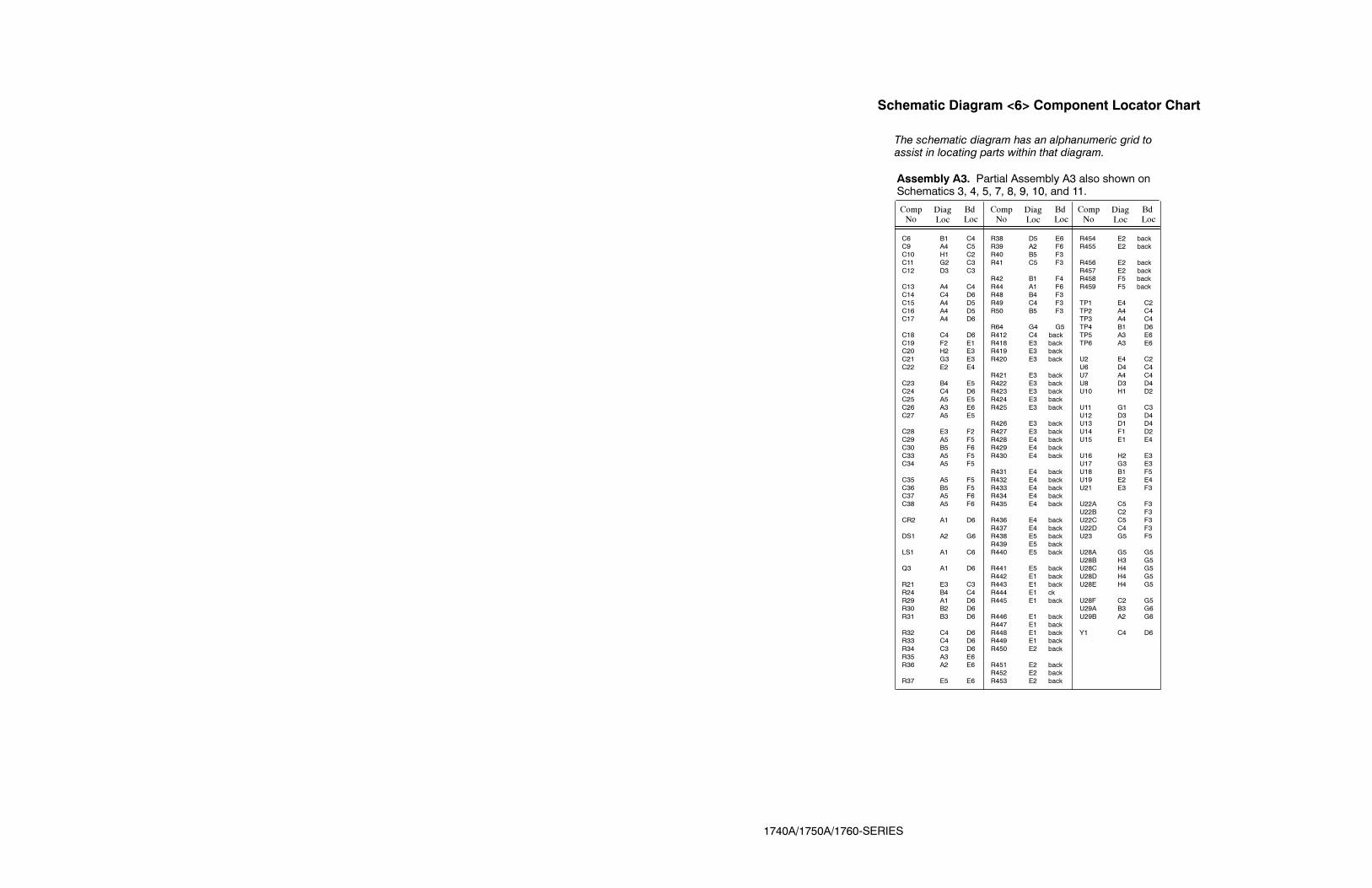
C6 B1 C4C9 A4 C5C10 H1 C2
C11 G2 C3
C12 D3 C3
C13 A4 C4C14 C4 D6
C15 A4 D5C16 A4 D5C17 A4 D6
C18 C4 D6
C19 F2 E1C20 H2 E3
C21 G3 E3
C22 E2 E4
C23 B4 E5C24 C4 D6
C25 A5 E5
C26 A3 E6
C27 A5 E5
C28 E3 F2
C29 A5 F5
C30 B5 F6
C33 A5 F5C34 A5 F5
C35 A5 F5
C36 B5 F5C37 A5 F6
C38 A5 F6
CR2 A1 D6
DS1 A2 G6
LS1 A1 C6
Q3 A1 D6
R21 E3 C3
R24 B4 C4
R29 A1 D6R30 B2 D6
R31 B3 D6
R32 C4 D6R33 C4 D6
R34 C3 D6
R35 A3 E6
R36 A2 E6
R37 E5 E6
R38 D5 E6R39 A2 F6R40 B5 F3
R41 C5 F3
R42 B1 F4
R44 A1 F6R48 B4 F3
R49 C4 F3R50 B5 F3
R64 G4 G5
R412 C4 back
R418 E3 backR419 E3 back
R420 E3 back
R421 E3 back
R422 E3 backR423 E3 back
R424 E3 back
R425 E3 back
R426 E3 back
R427 E3 back
R428 E4 back
R429 E4 back
R430 E4 back
R431 E4 back
R432 E4 back
R433 E4 backR434 E4 back
R435 E4 back
R436 E4 back
R437 E4 backR438 E5 back
R439 E5 back
R440 E5 back
R441 E5 backR442 E1 back
R443 E1 back
R444 E1 ck
R445 E1 back
R446 E1 back
R447 E1 back
R448 E1 backR449 E1 back
R450 E2 back
R451 E2 backR452 E2 back
R453 E2 back
R454 E2 backR455 E2 back
R456 E2 back
R457 E2 backR458 F5 backR459 F5 back
TP1 E4 C2
TP2 A4 C4TP3 A4 C4
TP4 B1 D6
TP5 A3 E6
TP6 A3 E6
U2 E4 C2
U6 D4 C4
U7 A4 C4
U8 D3 D4U10 H1 D2
U11 G1 C3
U12 D3 D4U13 D1 D4
U14 F1 D2
U15 E1 E4
U16 H2 E3U17 G3 E3
U18 B1 F5
U19 E2 E4
U21 E3 F3
U22A C5 F3
U22B C2 F3
U22C C5 F3
U22D C4 F3U23 G5 F5
U28A G5 G5
U28B H3 G5U28C H4 G5U28D H4 G5
U28E H4 G5
U28F C2 G5U29A B3 G6
U29B A2 G6
Y1 C4 D6
Schematic Diagram <6> Component Locator Chart
The schematic diagram has an alphanumeric grid toassist in locating parts within that diagram.
Assembly A3. Partial Assembly A3 also shown onSchematics 3, 4, 5, 7, 8, 9, 10, and 11.
CompNo
DiagLoc
BdLoc
CompNo
DiagLoc
BdLoc
CompNo
DiagLoc
BdLoc
1740A/1750A/1760-SERIES

BA[0..23]
A2 A3 E2
<7> <10><8>
FLASH EPROM
BA[0..23]BD[0..15]
BD[0..15]
BD[0..15]
A1 A1 H2
<7> <10><8>
BD7
A12
B118
A23
B217
A34
B316
A45
B415
A56
B514
A67
B613
A78
B712
A89
B811
DIR1
G19
U1574F245
DATA
BUFFERSR442 75.0
R443 75.0
ROM
A012
A111
A210
A39
A48
A57
A66
A75
A827
A926
A1023
A1125
A124
A1328
A1429
A153
A162
CE22
OE24
VPP1
PGM31
O013
O114
O215
O317
O418
O519
O620
O721
NC30
U1327C010
MICROPROCESSORR424.75K
+5V
+5V
TP4
R44332
+5V
DS1
<7>
C2
C5
R291.00K
INT_H_TPUINT_V_TPUREF_H_TPUREF_V_TPU
+5V
C610UF
21
3
CR2
Q3
A0A1A2A3A4A5A6A7A8A9A10A11A12A13A14A15A16A17
PIN128
+5V
VDD1
VDD7
VDD18
VDD28
VDD39
VDD50
VDD63
VDD65
VDD84
VDD96
VDD107
VDD116
VDD126
T2CLK128
TP016
TP115
TP214
TP313
TP412
TP511
TP610
TP79
TP86
TP95
TP104
TP113
TP12132
TP13131
TP14130
TP15129
IRQ177
IRQ276
IRQ375
IRQ474
IRQ573
IRQ672
IRQ771
BERR70
HALT69
RESET68
RXD53
TXD52
SCK45
MISO43
MOSI44
PCS0/SS46
PCS147
PCS248
PCS349
VSTBY19
VSS2
VSS8
VSS17
VSS29
VSS34
VSS40
VSS51
VSS59
VSS67
VSS83
VSS95
VSS101
VSS106
VSS117
VSS127
A090
A120
A221
A322
A423
A524
A625
A726
A827
A930
A1031
A1132
A1233
A1335
A1436
A1537
A1638
A1741
A1842
A19/CS6121
A20/CS7122
A21/CS8123
A22/CS9124
A23/CS10125
D0111
D1110
D2109
D3108
D4105
D5104
D6103
D7102
D8100
D999
D1098
D1197
D1294
D1393
D1492
D1591
AS82
DS85
R/W79
DSACK089
DSACK188
SIZ081
SIZ180
RMC86
AVEC87
BKPT/DSCLK56
IPIPE/DS054
IFETCH/DS155
FREEZE/QUOT58
TSTME/TSC57
CSBOOT112
BR/CS0113
BG/CS1114
BGACK/CS2115
FC0/CS3118
FC1/CS4119
FC2/CS5120
CLKOUT66
MODCK78
VDDSYN61
XFC64
EXTAL62
XTAL60
U18MC68332
C22.1UF
A1
A2
A3
A4
A5
A6
A7
A8
A9
A10
A11
A0
+5V
D0
D1
D2
D3
D4
D5
D6
D7D8
D9
D10
D11
D12
D13
D14
D15
/R/W
R444 75.0
R445 75.0
R446 75.0
R447 75.0
R448 75.0
R449 75.0
NOVRAM
A010
A19
A28
A37
A46
A55
A64
A73
A825
A924
A1021
A1123
A122
WE27
D011
D112
D213
D315
D416
D517
D618
D719
OE22
A13/NC26
A14/NC1
CE20
U14DS1225D
BA0
BA1
BA2
BA3
BA4
BA5
BA6
BA7
BA8
BD8
BD9
BD10
BD11
BD12
BD13
BD14
BD15BD0
BD1
BD2
BD3
BD4
BD5
BD6 RAM
A012
A111
A210
A39
A48
A57
A66
A75
A827
A926
A1023
A1125
A124
A1328
A143
A1531
A162
IO013
IO114
IO215
IO317
IO418
IO519
IO620
IO721
CS122
CS230
WE29
OE24
U11HM628128
BA1
BA2
BA3
BA4
BA5
BA6
BA7
BA8
BA9
BD0
BD1
BD2
BD3
BD4
BD5
BD6
BD7
BA1BA2BA3BA4BA5BA6BA7BA8BA9BA10BA11BA12BA13BA14BA15BA16BA17BA18
C10.1UF
BD0BD1BD2BD3BD4BD5BD6BD7
+5V
+5V
A012
A111
A210
A39
A48
A57
A66
A75
A827
A926
A1023
A1125
A124
A1328
A1429
A153
A162
D013
D114
D215
D317
D418
D519
D620
D721
VPP1
OE24
CE22
WE31
A1730
GND16
VCC32
U1028F020
C2010UF
BD8BD9BD10BD11BD12BD13BD14BD15
+5V
A012
A111
A210
A39
A48
A57
A66
A75
A827
A926
A1023
A1125
A124
A1328
A1429
A153
A162
D013
D114
D215
D317
D418
D519
D620
D721
VPP1
OE24
CE22
WE31
A1730
GND16
VCC32
U1628F020
C11.1UF
BA10
BA11
BA12
BA13
BA14
BA15
BA16
BA17
BA1BA2BA3BA4BA5BA6BA7BA8BA9BA10BA11BA12BA13BA14BA15
/SRAM
/FLASH
/WR_LO
/RD_LO
/RD_LO
/WR_LO
+5V
+5V
NC
NC
C19.1UF
BA9
BA10
BA11
BA12
R/W
+5V
BD8
BD9
BD10
BD11
BD12
BD13
BD14
BD15
A12
B118
A23
B217
A34
B316
A45
B415
A56
B514
A67
B613
A78
B712
A89
B811
DIR1
G19
U1974F245
D8
D9
D10
D11
D12
D13
D14
D15
/DATA_EN2
/R/W
R450 75.0
R451 75.0
R452 75.0
R453 75.0
R454 75.0
R455 75.0
R456 75.0
R457 75.013 12
U28F74F04
56
4
U22B74HCT125
A12
A13
A14
A15
/CSBOOT
A16
A17
/RST
+5V
D0D1D2D3D4D5D6D7D8D9D10D11
A18
A19A20A21A22A23
<7>
<4>
<8>
C4
C3C3
C3
A4
C2C3
C3
A4
R394.75K
DONE/PROG1
DONE/PROG2
TIME_CODE1
H_CAL
TPU_FIELDMOD_VPULSE
FIELD_IDFREE_H_EN
SPARE2SPARE1
IRQ1
IRQ1
IRQ2
IRQ5
/ADDR_EN/DATA_EN
DONE/PROG1DONE/PROG2
BEEP
+5V
+5V
<10>
H4
56
4
U29B74HCT125
IRQ2
<10>
<7>
<9>
H4
F2
A4
IRQ5
IRQ6
IRQ7
<9>
<10>
<9>
A4
A1
B1
R314.75K
R304.75K
R354.75K
R364.75K
RXDTXD
/PCS0/PCS1/PCS2/PCS3
/BERR/HALT
IRQ7
SCK
MOSIBMISO
IRQ6
/RST+5V
TP6
R344.75K
D12D13D14D15
/AS
SIZ0SIZ1
/DS
PIN128
R/W
+5V
BUFFERS
<10>
H3
A12
B118
A23
B217
A34
B316
A45
B415
A56
B514
A67
B613
A78
B712
A89
B811
DIR1
G19
U874F245
DSACK0DSACK1
A0
A1
A2
A3
A4
A5
A6
A7
ADDRESS
A1
B2
C3
G16
G2A4
G2B5
Y015
Y114
Y213
Y312
Y411
Y510
Y69
Y77
U2174F138
BA16
BA17
BA18
/DECODE
+5V
DECODERS
BA2
BA3
BA4
BA5
BA6
BA7R418 75.0
R419 75.0
R420 75.0
R421 75.0
R422 75.0
R423 75.0
R424 75.0
<7>
<8>
NC
NC
<10>
<8>
A2
C4
A2
F5
/HRAM_CS
/LRCTRL
/RDCTRL
/P_OPT_CS
A012
A111
A210
A39
A48
A57
A66
A75
A827
A926
A1023
A1125
A124
A1328
A143
A1531
A162
IO013
IO114
IO215
IO317
IO418
IO519
IO620
IO721
CS122
CS230
WE29
OE24
U17HM628128
BA1
BA2
BA3
BA4
BA5
BA6
BA7
BD8
BD9
BD10
BD11
BD12
BD13
BD14
BA16BA17BA18
/FLASH/WR_HI
/RD_HIFLASH
<11>
C2
VPP1
+5V
NC
NC
NC
3 4
U28B74F04
5 6
U28C74F04
9 8
U28D74F04
C21.1UF
BA8
BA9
BA10
BA11
BA12
BA13
BA14
BA15
BA16
BA17
BD15
/SRAM
+5V
NC
NC
16
1
2
3
4
5
6
7
8
9
10
11
12
13
14
15
R214.7K
RESIN
/RST
/LDS
/DATA_EN2
/RD_HI
/RD_LO
/ADDR_EN2
+5V
C28.1UF
C12.1UF
/ADDR_EN
+5V
+5V
BA0
BA1
BA8
BA9
BA10
BA11
BA12
BA13
R425 75.0
R426 75.0
R427 75.0
R428 75.0
R429 75.0
R430 75.0
R431 75.0
A12
B118
A23
B217
A34
B316
A45
B415
A56
B514
A67
B613
A78
B712
A89
B811
DIR1
G19
U1274F245
A8
A9
A10
A11
A12
A13
A14
+5VNCNC
C24.1UF
/CSBOOT
PIN128
/SRAM/FLASH
/BR1/BG1/BGACK1/DECODE
+5V
+5V
16MHZ
R41256.2
H4 H4
C261UF
23
1
U29A74HCT125
RESIN
/RST<11>
TP5
RESET
ABORT
A3 A4
/RESET
<7> <10><8>
TP2
TP3
C93.3UF
C15.1UF
+5V<10>
U18 VDD FILTER CAPS
R2410.0K
C13.1UF
RESIN2
SENSE7
GND4
VCC8
RST5
RST6
REF1
CT3
U7TL7705
C23.1UF
C17.1UF
C16.1UF
/BR
+5V+5V+5V
+5V
+5V
H4
R3210.0M
1 2
34
Y132.768KHZ
R33332K
C1822PF
12 11
13
U22D74HCT125
R4810.0K
R4910.0K
/BR1
+5V+5VA1
2B1
18
A23
B217
A34
B316
A45
B415
A56
B514
A67
B613
A78
B712
A89
B811
DIR1
G19
U674F245C14
22PF
A15
A16
A17
A18
A19
A20
+5V
TP1
BA14
BA15
BA16
BA17
BA18
BA19
BA20
R432 75.0
R433 75.0
R434 75.0
R435 75.0
R436 75.0
R437 75.0
R438 75.0
H4
D1
<9>
<7>
/UDS MISO/UDS
R/W
/WR_LO
/WR_HI
/DS
/UDS
DONE/PROG1
DONE/PROG2
R45875.0
1A12
1Y118
1A24
1Y216
1A36
1Y314
1A48
1Y412
2A111
2Y19
2A213
2Y27
2A315
2Y35
2A417
2Y43
1G1
2G19
U2374F244
R6410.0K
BMISO
/WR_HI
/RD_HI
+5V
+5V
BUFFERED
OUTPUT
NC
H4 B1 D3 C5
H4 B1 F4 C4
11 10
U28E74F04
BSCK
BMOSI
<7> <9> <10> <11>
<7> <9> <10> <11>
<10>
A4 A4 H4
A2 A2 H4
H4
/BAS
BR/W
B16MHZ
<7> <10><8>
<7> <10><8>
NC
NCNC
NC
1 2
U28A74F04
SCK
MOSI
/AS
16MHZ
R/W
<10>
H4
E3
<11>
<10>D3
/LDS/LDS
/DATA_EN2
/ADDR_EN2
/RD_HI
/RD_LO
/WR_HI
/WR_LO
R45975.0
NC
R384.75K
R374.75K
I/CK1
I2
I3
I4
I5
I6
I7
I8
I9
I/O19
I/O18
I/O17
I/O16
I/O15
I/O14
I/O13
I/O12
I/OE11
U216V8
BA0
SIZ1
SIZ0
R/W
/DS
/CSBOOT
/DATA_EN
/ADDR_EN
/BGACK
+5V
+5V
BA21
BA22
BA23
R439 75.0
R440 75.0
R441 75.0
A21
A22
A23
/ADDR_EN2
+5VH4
98
10 U22C
74HCT125
2 3
1
U22A74HCT125
R5010.0K
R4010.0K
R4110.0K
/BG1
/BGACK1
+5V
+5V
+5V
<10>
PIN 95 PIN 83 PIN 59
PIN 40 PIN 67
PIN 29
PIN 2
PIN 127 PIN 117
C38.1UF
C36.1UF
C27.1UF
C29.1UF
C30.1UF
C35.1UF
C34.1UF
/BG
/ADDR_EN
/ADDR_EN
+5V
+5V +5V+5V
+5V
+5V+5V
PIN 101
PIN 34
PIN 51
C37.1UF
C25.1UF
C33.1UF
+5V
+5V
+5V
PIN 8
1740A/1750A/1760--SERIES
<10>
PIN 17 H4
/BGACK/BGACK
MICROPROCESSOR <6>
AND SERIAL NUMBER RANGES.SEE PARTS LIST FOR EARLIER VALUESNOTE:
PART OF A3 MAIN BOARD

C40 C5 F2C50 D2 H2C51 C4 H4
C52 C4 I4
C57 G2 I2
C58 E2 I5C62 G1 I3
C63 G4 I3
C67 G3 J3
C71 G5 J3
C106 E4 L2
C108 E4 M2
C110 E3 L3
C113 E4 M2
C115 E3 M3
C116 E3 M4
J9 H2 K6
Q4 B5 G3Q5 B5 G3
Q6 C5 G3
Q29 B5 G2
R57 B4 G3R62 C5 G2
R63 B5 G2R65 B5 G2
R66 C4 G3R67 B4 G3
R68 C5 G3R69 C4 G3
R70 C5 G3
R78 D2 H2R79 D2 H2
R87 C4 H4
R88 C2 I4
R99 A4 I2R109 C2 I5
R234 E3 L2
R235 E4 M2R241 E3 M3
R243 E3 M3
R262 H2 M4
R358 A3 G3R361 C3 P6
R378 B5 G2R379 B5 G2
U26A A5 F3U26B A5 F3
U26C B5 F3U26D A5 F3
U34 B1 I2
U40 E1 I4U42 F1 I2
U43 F2 I3
U44 F3 I3
U51 F3 I3U52 F4 I3
U68 E4 M2
U71 E3 M3U93 A3 G3
Schematic Diagram <7> Component Locator Chart
The schematic diagram has an alphanumeric grid toassist in locating parts within that diagram.
Assembly A3. Partial Assembly A3 also shown onSchematics 3, 4, 5, 6, 8, 9, 10, and 11.
CompNo
DiagLoc
BdLoc
CompNo
DiagLoc
BdLoc
CompNo
DiagLoc
BdLoc
1740A/1750A/1760-SERIES

V_INT_SEL
OUTPUTS
SYNCHRONOUS
D12
Q119
D23
Q218
D34
Q317
D45
Q416
D56
Q515
D67
Q614
D78
Q713
D89
Q812
CLK11
OC1
U4274HCT574
FD8
BD[0..15]BD[0..15]<6>
F1
BD[0..15]
LINE RATE
CONTROLLER
D0---DIN--- I/O72
D1--- I/O70
D2--- I/O67
D3--- I/O65
D4--- I/O62
D5--- I/O60
D6--- I/O58
D7--- I/O56
CS0--- I/O61
CS1--- I/O66
A0---WS--- I/O75
A1---CS2--- I/O76
A2--- I/O77
A3--- I/O78
A4--- I/O82
A5--- I/O84
A6--- I/O3
A7--- I/O5
A8--- I/O9
A9--- I/O11
A10--- I/O10
A11--- I/O8
A12--- I/O4
A13--- I/O2
A14--- I/O83
A15--- I/O81
DOUT--- I/O73
HDC--- I/O34
LDC--- I/O36
INIT--- I/O42
RDY/BSY---RCK--- I/O71
RESET54
M0---RTRIG32
M1---RDATA31
M2--- I/O33
DONE---PG55
CCLK74
TCLKIN--- I/O13
XTL1---BCLKIN--- I/O57
XTL2--- I/O53
I/O6
I/O7
I/O14
I/O15
I/O16
I/O17
I/O18
I/O19
I/O20
I/O21
I/O23
I/O24
I/O25
I/O26
I/O27
I/O28
I/O29
I/O30
I/O35
I/O37
I/O38
I/O39
I/O40
I/O41
I/O44
I/O45
I/O46
I/O47
I/O48
I/O49
I/O50
I/O51
I/O52
I/O59
I/O63
I/O68
I/O69
I/O79
I/O80
PWRDN12
VCC22
VCC64
GND43
GND1
U34XC3042
BD8
BD9
BD10
BD11
BD12
BD13
BD14INT_H_TPU
FD10
FD11
REF_V_SYNC
REF_H_SYNC
INT_V_SYNC
INT_H_SYNC
NC
Q010
Q111
Q213
Q314
Q419
Q520
Q621
Q722
Q815
XO/HF23
D83
D728
D629
D530
D431
D34
D25
D16
D07
W2
R18
RS25
FL/RT26
XI8
FF9
EF24
DGND16
VCC32
U407201
BD8
BD9
BD10
BD11
BD12
BD13
BD14
BD15
NC
NC
A3
FD9
FD10
FD11
FD12
FD13
FD14
FD15
/L1
FD8
FD9
FD10
FD11
FD12
FD13
FD14
FD15
<9>
<11>
<11>
<11>
<11>
<9>
<9>
<9>
E3
E4
E5
E4
G5
H5
G3
H3
C62.1UF
RO_INT_SEL
PX_INT_SEL
W_INT_SEL
V_POS_SEL0
V_POS_SEL1
VGAIN_SEL0
VGAIN_SEL1
+5V
1A1
1B2
2A3
2B4
3A5
3B6
4A7
4B8
5A9
5B10
6A11
6B12
7A13
7B14
8A15
8B16
9A17
9B18
10A19
10B20
11A21
11B22
12A23
12B24
13A25
13B26
14A27
14B28
15A29
15B30
16A31
16B32
17A33
17B34
J9
<9>
<5>NC
<9>
<9>
<9>
<9>
<5>
G1
H1
G4
H4
G2
E4
E4
C57.1UF
H_MAG_SEL0
H_MAG_SEL1
H_POS_SEL1
H_POS_SEL0
HGAIN_SEL0
HGAIN_SEL1
FOCUS_SEL
+5V
NC<6>
C58.1UF
D12
Q119
D23
Q218
D34
Q317
D45
Q416
D56
Q515
D67
Q614
D78
Q713
D89
Q812
CLK11
OC1
U4374HCT574
IRQ6FD8
FD9
FD10
FD11
FD12
FD13
FD14
FD15
/L2
+5V
/LR_RD
/LR_RESET
/LR_RETRAN
/LR_WR
B2 B1
<3>
R792.21K
R781.82K
C50330PF
CLAMP_PLS
<6>
<6>
B1INT_V_TPU
REF_H_TPU
REF_V_TPU
FREE_H_EN
/START
DEMOD_CLMP
SYNC_GATE
ST_SAMPLE
CHROM_GATE
R88499
/LRCTRL
BR/W
BD15
BA[0..23]
BA1
BA0
/L1
/L2
/LR_RD
/LR_WR
BA2
<6>
<6>
<6>
F3
H5
H1
BA[0..23]
NC
+5V VCC4
GND2
NC1
OUT3
U936MHZ
/L3
FD8
FD9
FD12
/L5
FD13
FD14
FD15
/L4
R358562
<3>
NC
<6>
<10>
<11>
<6>
<5>
<5>
<6>
PIX_STROBE
OPTION_PLS
OFFSCREEN
HRETRACE
A/D_CLK
FIELD_ID
SPARE1
SPARE2
/LS_STROBE
VEC_SCH_SW
BURST_GATE
R109499
H5
F1
B2
B2
C5
B2
G4
B2
INT_H_SYNC
INT_V_SYNC
NC
NC
SYNC
SEPARATOR
V+8
VID IN2
TIMING6
GND4
BP5
INDEX7
FIELD3
SYNC1
U71LM1881
C110.1UF
C115.1UF
C116.1UF
+5V
R243681K
R24110.0
<3>
E1
D12
Q119
D23
Q218
D34
Q317
D45
Q416
D56
Q515
D67
Q614
D78
Q713
D89
Q812
CLK11
OC1
U5174HCT574
INT_VIDEO
FD8
FD9
FD10
FD11
FD12
FD13
FD14
<3>
<4>
<4>
<11>
H4
H3
H3
C2
C4
B2
F3
B3
INPUT_SEL0
INPUT_SEL2
INPUT_SEL1
/AUX0
/AUX1
/AUX2
X_BLNK_EN
VEC_CHROM+
B---Y
R---Y
REF_VIDEO
INT_VIDEO
<5><3>
<4><3>
R262100
+5V
J9CONNECTS
TO P1
<13>
A5VECTORBOARD
---11V
+11V
+5V
<5>
<8>
<5>
B3
D3
C3
C4
C67.1UF
X_HORZ_SEL
H_SIG_SEL2
H_SIG_SEL1
H_SIG_SEL0
/AUX3
RO_START
FILTER_SEL0
SCH_FIELD
DEMOD_CLMP
VEC_SCH_SW
ODD_FIELD
SYNC_GATE
BLANK_CK
ST_SAMPLE
BURST_GATE
+5V
<3>
G2
D12
Q119
D23
Q218
D34
Q317
D45
Q416
D56
Q515
D67
Q614
D78
Q713
D89
Q812
CLK11
OC1
U4474HCT574
REF_VIDEO
FD15
FD8
FD9
FD10
FD11
FD12
FD13
/L3
NC
NC
V+8
VID IN2
TIMING6
GND4
BP5
INDEX7
FIELD3
SYNC1
U68LM1881
C106.1UF
C108.1UF
C113.1UF
+5V
R235681K
R23410.0
<10>
B2
C3
B2
B2
C1
F4
H4
BLANK_CK
REF_H_SYNC
REF_V_SYNC
<5>
<11>
<10>
<6>
<6>
<6>
R8710.0K
REMOTE_SYNC
TPU_FIELD
H_CAL
MOD_VPULSE
FLD_RETR
/BLANK
/LR_RESET
/LR_RETRAN
SCH_FIELD
BLANK_CK
+5V
R361
392<4>
NC
NC
NC
<6>
<6>
B2
A4
B2
R9910.0K
/RESET
DONE/PROG1
CAL_TIMING
+5V
<8>
<6>
H4
C3
R6739.2
B16MHZ
RO_BLANK
+5V
+5V
C511UF
R57562
C52.1UF
R66182
R69274
ODD_FIELD
+5V
+5V+5V
15
17
19
12
U26CMC10H103
D12
Q119
D23
Q218
D34
Q317
D45
Q416
D56
Q515
D67
Q614
D78
Q713
D89
Q812
CLK11
OC1
U5274HCT574
FD14
FD15
FD8
FD9
FD10
FD11
FD12
/L4
<4>
<9>
<6>
<5>
<4>
<4>
<4>
<6>
<6>
<9>
E3
E4
D2
D2
B2
B2
F4
H4
H4
C63.1UF
H_RO_SEL
V_RO_SEL
V_MAG_0
V_MAG_1
/LS_STROBE
/VEC_EN
/VEC_CS
MISO
BSCK
BMOSI
FILTER_SEL1
FILTER_SEL2
/LS_STROBE
CHROM_GATE
A/B
+5V
F3
<11>NC
NC
C71.1UF
A/B
+5V
FD13
FD14
FD15
/L5
/START
R621.50K
R68274
R70825
C40470PF
---8V
Q5
Q29
Q6
NC
NC
NC
10MHZ---TTL
5
7
32
20
10
U26AMC10H103
13
14
18
U26DMC10H103
8
9
4
U26BMC10H103
R65182 R63
200
R378681
R37918.2
Q4
NC
NC
NC
NC
NC
NC
1740A/1750A/1760--SERIES
---8VNOTE:
DYNAMIC CONTROL <7>
PART OF A3 MAIN BOARDAND SERIAL NUMBER BREAKS.SEE PARTS LIST FOR EARLIER VALUES

C31 C4 F4C32 C4 F4C53 E4 H5
C54 E4 H5
C65 F4 I6
C68 H4 J6C69 F5 J6
C70 H3 J6
C77 G3 J5
C87 G3 K6
C182 D5 J6
R58 C4 F5
R72 B4 G5
R89 E4 H5
R90 E4 H5
R103 F4 I6R104 F5 I6
R105 F3 I6R106 F3 I6
R114 F5 I6
R115 F4 I6
R116 F3 I6
R117 F3 I6
R120 G5 I6
R121 G3 I6
R134 G4 J6
R135 G3 J6
R376 G3 K6
R377 D4 J6
TP7 G4 I6
U27 B1 F4
U36 D2 H4U37 E3 H5U48A F4 J6
U48B F3 J6
U48C H3 J6
U48D H5 J6U54A G3 J6
U54B D4 J6
U54C G5 J6U54D D5 J6
Schematic Diagram <8> Component Locator Chart
The schematic diagram has an alphanumeric grid toassist in locating parts within that diagram.
Assembly A3. Partial Assembly A3 also shown onSchematics 3, 4, 5, 6, 7, 9, 10, and 11.
CompNo
DiagLoc
BdLoc
CompNo
DiagLoc
BdLoc
CompNo
DiagLoc
BdLoc
1740A/1750A/1760-SERIES

<6>
F1
BD[0..15]BD[0..15]
BD8
BD9
BD10
BD11
BD12
BD13
READOUT CONTROL
NC
D0---DIN--- I/O72
D1--- I/O70
D2--- I/O67
D3--- I/O65
D4--- I/O62
D5--- I/O60
D6--- I/O58
D7--- I/O56
CS0--- I/O61
CS1--- I/O66
A0---WS--- I/O75
A1---CS2--- I/O76
A2--- I/O77
A3--- I/O78
A4--- I/O82
A5--- I/O84
A6--- I/O3
A7--- I/O5
A8--- I/O9
A9--- I/O11
A10--- I/O10
A11--- I/O8
A12--- I/O4
A13--- I/O2
A14--- I/O83
A15--- I/O81
DOUT--- I/O73
HDC--- I/O34
LDC--- I/O36
INIT--- I/O42
RDY/BSY---RCK--- I/O71
RESET54
M0---RTRIG32
M1---RDATA31
M2--- I/O33
DONE---PG55
CCLK74
TCLKIN--- I/O13
XTL1---BCLKIN--- I/O57
XTL2--- I/O53
I/O6
I/O7
I/O14
I/O15
I/O16
I/O17
I/O18
I/O19
I/O20
I/O21
I/O23
I/O24
I/O25
I/O26
I/O27
I/O28
I/O29
I/O30
I/O35
I/O37
I/O38
I/O39
I/O40
I/O41
I/O44
I/O45
I/O46
I/O47
I/O48
I/O49
I/O50
I/O51
I/O52
I/O59
I/O63
I/O68
I/O69
I/O79
I/O80
PWRDN12
VCC22
VCC64
GND43
GND1
U27XC3030
/SAMPLE
DAC_A0
/SAMPLE
smpl hold
/LDAC
2.8US 3.6US
1US
/SAMPLE
stroke
.5US
RO_BLANK
R0
R1
R2
R3
R4
R5
R6
R7
A010
A19
A28
A37
A46
A55
A64
A73
A825
A924
A1021
A1123
A122
D011
D112
D213
D315
D416
D517
D618
D719
CS120
CS226
WE27
OE22
U366264LFP
A0
A1
A2
A3
A4
A5
A6
A7
A8
A9
A10
A11
A0
A1
A2
A3
A4
A5
A6
A7
A8
A9
<6>
<6>
F3
H5
/RDCTRL
BR/W
BD14
BD15
BA1
BA0
BA2
BA3
BA4
BA5
<6>
H1
BA[0..23]BA[0..23]
BA6
BA7
BA8
BA9
BA10
BA11
BA12
/RAM_RD
/LDAC
RO_INTENS0
RO_INTENS1
RO_INTENS2
RO_START
RO_BLANK
R0
R1
R2
A10
A11
A12
<7>
<7>
<11>
G4
A4
E4
A12
/RAM_RD
/RAM_WR
/RAM_CS
+5V
<9>
G5
DB0/815
DB1/914
DB2/1013
DB3/1111
DB410
DB59
DB68
DB77
A016
A117
LDAC20
WR19
CS18
REF INA1
REF INB3
REF OUT2
VSS23
AGND6
DGND12
VDD21
VOUTA22
ROFSA24
VOUTB5
ROFSB4
U37AD7237
RO_V_OFFSET
R0
R1
R2
6
57
U48BMC34004
R1162.74K
R1062.74K
R1056.81K
V SHAPE
READOUT STROKE
GENERATOR
12 14
10
U54DSMP04
R1355K
R4644.75K <4>
C5
9
108
U48CMC34004
V_RO_SIG
C70330PF
R1214.75K
TP7
R1171.50K
C54.1UF
R9022.1
R3
R4
R5
R6
R7
DAC_A1
/LWR_CS
/LDAC
DAC_A0+8V
<6> F3/LDAC
DAC_A0
+5V
NC
R5810.0K
/HRAM_CS
R3
R4
R5
R6
R7
/RAM_WR
/RAM_CS
DAC_A1
/LWR_CS
NC
NC
<6>
<6>
A4
B2
R724.75K
/RESET
DONE/PROG2
+5V
+5V
NC
NC
<6>
H5
B16MHZ
C311UF
C32.1UF
<9>
G4
<9>
G45 1
7
U54BSMP04
RO_H_CAL
RO_V_CAL
R377100K
R48010K NC
R8922.1
C53.1UF
---8V
R1032.74K
R1152.74K
C65.1UF
2
31
4
11
U48AMC34004
+8V
H SHAPE
11 15
9
U54CSMP04
R1345K
R4654.75K <5>
C4
13
1214
U48DMC34004
C68330PF
H_RO_SIG
R1204.75K
R1046.81K
R1141.50K
C69.1UF---8V
<9>
NC
G4
3 2
16
6
813
U54ASMP04
C77.1UF
C871UF
RO_H_OFFSET+8V
R376221
C182.1UF
1740A/1750A/1760--SERIES
---8VNOTE:
READOUT <8>
AND SERIAL NUMBER RANGES.SEE PARTS LIST FOR EARLIER VALUES
PART OF A3 MAIN BOARD

C41 E5 G2C44 F5 G1C46 B5 G6
C48 F3 G2
C49 E3 H1
C59 G3 I1C60 G1 I2
C61 G4 I2
C66 G2 J1
C162 F2 O1
C163 F2 O1
C180 E3 H2
Q24 D4 O3
R23 B5 C5
R25 B5 C5R26 B5 C5
R27 B5 C5
R28 A4 D6R52 F4 G1
R53 F5 G1
R55 E4 G2
R59 E3 G1R60 F2 G2
R61 F4 G2
R80 G3 H2
R81 G3 H2
R82 C2 H6
R84 G2 H2
R85 G3 H2
R91 G4 I1R92 G4 I1
R93 G4 I1
R94 G3 I1
R95 G3 I1
R96 G3 I1
R97 G5 I1
R107 G3 I1
R108 G1 I2
R123 G2 J1
R127 * H4 H2
R319 D4 O3R320 D4 O3
R336 F2 P2
R337 E1 P2
R338 F1 P2R362 E3 H2
R363 E4 I2
S1 A5 C6
TP10 E2 O1
U9 B4 C5
U24 A1 F6U25A E4 G2
U25B C4 G2
U25C E4 G2U25D E4 G2
U29D C3 G6
U30A E2 G2
U30B E2 G2
U30C C1 G2U30D E3 G2
U31 F4 G1
U32 B2 H6U33 E5 H2
U35 F3 H1
U38 B1 H6
U39C G4 I2U39D G1 I2
U41A H3 I1
U41B G5 I1
U41C H5 I1
U45A G3 I1
U45B G2 I1
U46A G4 I1
U46B H3 I1
U46C G3 I1
U50A H2 J2
U50B G1 J2
U50C H1 J2
U77 C3 M3
U82 C4 O3
U85 E2 O1
U86 F1 O1
U87A E1 O2
U87B E1 O2U87C E1 O2
U94B H4 K2
U95 E3 H1
Schematic Diagram <9> Component Locator Chart
The schematic diagram has an alphanumeric gridto assist in locating parts within that diagram.
Assembly A3. Partial Assembly A3 also shown onSchematics 3, 4, 5, 6, 7, 8, 10, and 11.
CompNo
DiagLoc
BdLoc
CompNo
DiagLoc
BdLoc
CompNo
DiagLoc
BdLoc
1740A/1750A/1760-SERIES
* See Parts List for earlierserial number ranges.

C60.1UF
13
1214
U39DMC34004
R108100K
D/A CONVERTERS
R33810.0K
+5V
23
1
U87A74HCT125
MISO<6>
<11>
<11>
C4
C5
F4
MISO
/ADCS2
/ADCS1
/MN_ID_CSSER
14QA
15
QB1
SCLK11
QC2
SCLR10
QD3
QE4
RCLK12
QF5
G13
QG6
QH7
QH’9
U3874HC595
BMOSIBMOSI
<6>
B3
INTERFACE
/PCS0
/PCS1
/PCS2
/PCS3
SERIAL <6>
<11>
H4
H3
H4
Y01
Y12
Y23
Y34
Y45
Y56
Y67
Y78
Y89
Y910
Y1011
Y1113
Y1214
Y1315
Y1416
Y1517
CS219
CS118
A023
A122
A221
A320
U2474HCT154
BSCK
/FPAN_CS
/FPAN_EN
/VEC_CS
/MAIN1_CS
/MAIN1_EN
/MAIN2_CS
/MAIN2_EN9 8
10
U30C74HCT125
BSCK
+5V
/DAC2_CS
/DAC2_LD
/DAC3_CS
/DAC3_LD
/MN_ID_LD
/ADCS1
/ADCS2
MISO
R33710.0K
9 8
10 U87C
74HCT125
5 6
4U87B
74HCT125
/DAC1_LD
/DAC1_CS
BSCK
BMOSI
GND5
IN2
IN3
IN6
IN7
OUT1
U8579L05C191
1UF
FOCUS0
FOCUS1
H_GAIN0
H_GAIN2
H_GAIN3
SDO4
VOUT014
VOUT115
VOUT216
VOUT317
VOUT418
VOUT519
VOUT620
VOUT721
VOUT823
VOUT924
VOUT1025
VOUT1126
VOUT1227
VOUT1328
VOUT141
VOUT152
SDI8
VREFOUT11
VREFIN12
SCLK7
LD6
16/4 MODE5
RBIAS10
VDD3
DGND9
AGND22
VSS13
U86I10412
C163.1UF
CAL_LEVEL
VREF_A1
VREF_A2
VREF_A3
+5V
+5V
<4><7> <7>
A2G2 G2
HGAIN_SEL1HGAIN_SEL0
2
115
10
U50BMC14053
<5>
E4
F3
H_GAIN
+5V
5
34
9
U50CMC14053
<11>FOCUS
<3>
<7>
<5>
<3>
B2
<4>
<5>
G2
E4
A4
B1
A2
R12310.0K
C66.1UF
FOCUS_SEL
---8V
12
13146
11
16
7 8
U50AMC14053
R336475K
FLD_SWP_SPD
LN_SWP_SPD
VREF_B1
VREF_B2
CHROM_GAIN
CAL_OSC_PK
VREF_A
VREF_B3
VREF_B
C1621UF
NC
23
1
U30A74HCT125
MISO
---11V
R4162.4
TP10
---11V+2.5V
R460
3.32K
1
8
2 3 6 7
U96
TL431S08
R461
100 OHMS
C22210UF
<10>
D3/REMOTE_CS
/REMOTE_LD
/MN_ID_CS
/ADCS1
/ADCS2
/DAC2_CS
/DAC2_LD
/DAC3_CS
/DAC3_LD
+5V
SER14
QA15
QB1
SCLK11
QC2
SCLR10
QD3
QE4
RCLK12
QF5
G13
QG6
QH7
QH’9
U3274HC595
16
15
14
13
12
11
10987654321
R824.7K
BMOSI
NC
<7>
<10>
F4
/VEC_EN
/S_OPT_CS
/S_OPT_EN
12 11
13
U29D74HCT125
BSCK
/STATIC1
+5V
OUTPUTS
STATIC
SERIAL
/DAC1_CS
/DAC1_LD
MISOR5910.0K
12 11
13 U30D
74HCT125
C49.1UF
5 6
4U30B
74HCT125
/DAC2_LD
/DAC2_CS
BSCK
BMOSI
+8V OUT1
IN8
GND2
GND3
GND6
GND7
U9578L05
R6010.0K
SDO4
VOUT014
VOUT115
VOUT216
VOUT317
VOUT418
VOUT519
VOUT620
VOUT721
VOUT823
VOUT924
VOUT1025
VOUT1126
VOUT1227
VOUT1328
VOUT141
VOUT152
SDI8
VREFOUT11
VREFIN12
SCLK7
LD6
16/4 MODE5
RBIAS10
VDD3
DGND9
AGND22
VSS13
U35I10412
VPOS2
VPOS3
+5V
<7><7>
G1G1
R8439.2K
R8539.2K
R8039.2K
R8139.2K
6
57
U45BMC34002
R10718.2K
V_POS_SEL0 V_POS_SEL1
VPOS3
VPOS2 5
34
9
U46CMC14053
<4>
E3
V_POS
+5V
---8V
12
13146
11
16
7 8
U41AMC14053
<5>
E4
WFM_H_POS
2
115
10
U46BMC14053
<7>
G2
2
31
8
4
U45AMC34002
C59.1UF
H_POS_SEL1
HPOS0
+8V
+5V---8V
R91150K
R92150K
R93150K
R96150K
R95150K
R94150K
---8V
R127825
NC
R61475K
C481UF
<3>
C1801UF
23
1
U25A74HCT125
MISO
R462
100 OHMS
NC
A5
A5
D3
D3
D3
D2
E3
SER14
QA15
QB1
SCLK11
QC2
SCLR10
QD3
QE4
RCLK12
QF5
G13
QG6
QH7
QH’9
U7774HC595
NTSC/PAL
PAL/NTSC
REFCH_SEL0
REFCH_SEL1
REFCH_SEL2
REFCH_SEL3
INT/EXT
BMOSI
BSCK
+5V
<6>
NCA3
<6>
B3
16
12345678910
11
12
13
14
15
R284.7K
IRQ7
/BERR
/HALT
1234
8765
S1
260---1965
NCNC
+5V
NC
SER10
A11
B12
C13
D14
E3
F4
G5
H6
CLK2
CLKINH15
SH/LD1
QH9
QH7
U974HC165
5 6
4
U25B74HCT125
BMOSI
<3>
<3>
<10>
<3>
R31947.5K
SER14
QA15
QB1
SCLK11
QC2
SCLR10
QD3
QE4
RCLK12
QF5
G13
QG6
QH7
QH’9
U8274HC595
R32015.0K
SLOW/FAST
AC/DC_SEL
OUT_2
DCREST_ON
BSCK
+5V
---8V
+5V
Q24B2
B1
B2
D4
9 8
10 U25C
74HCT125
R5510.0K
12 11
13U25D
74HCT125/DAC3_CS
/DAC3_LD
BSCK
BMOSI
C1921UF
SDO4
VOUT014
VOUT115
VOUT216
VOUT317
VOUT418
VOUT519
VOUT620
VOUT721
VOUT823
VOUT924
VOUT1025
VOUT1126
VOUT1227
VOUT1328
VOUT141
VOUT152
SDI8
VREFOUT11
VREFIN12
SCLK7
LD6
16/4 MODE5
RBIAS10
VDD3
DGND9
AGND22
VSS13
U31I10412
R5210.0K
PIX_CONTRAST
RO_H_OFFSET
RO_H_CAL
RO_V_CAL
PIX_BK_LVL
CHROMA_VOS
HPOS3
HPOS2+5V
+5V
<8>
<7>
<4>
<5>
<5>
<8>
<8>
G2
E5
G4
G5
D4
E5
D4
C61.1UF
9
108
U39CMC34004
H_POS_SEL0
---8V
12
13146
11
16
7 8
U46AMC14053
<5>
E4
H_POS2
115
10
U94BMC14053
<4>
E3
V_GAIN
5
34
9
U41CMC14053
<7>
<11>
<8>
<11>
<11>
<11>
<11>
G1
G1
E3
G4
F1
E4
E5
E4
R97100K
VGAIN_SEL0
VGAIN_SEL1
2
115
10
U41BMC14053
V_GAIN2
V_GAIN3
V_GAIN0
C44.1UF
TRACE_ROT
GRAT_LITES
RO_V_OFFSET
WFM_INT
VEC_INT
RO_INT
+5V
R53475K
C411UF
NC
D4
D4
D4
D2
---8V
GND5
IN2
IN3
IN6
IN7
OUT1
U3379L05
R4172.4
NC
<10>
<10>
<3>
<3>
/OSC_SEL
OSC_SEL
SER_LINK
OUT_1
/MN_ID_LD
/MN_ID_CS/MN_ID_CS
BSCK
/MN_ID_LD
/STATIC1
R270 OHM
R230 OHM
R260 OHM
R250 OHM
C46.1UF
/MN_ID_LD
+5V
1740A/1750A/1760--SERIES
NOTE:
<7>
DACS & SERIAL <9>
AND SERIAL NUMBER RANGES.SEE PARTS LIST FOR EARLIER VALUES
PART OF A3 MAIN BOARD

C170 C1 P1C171 B1 P3
C172 C1 P2
C173 D5 P5
C174 E5 P6C175 B1 P1
J2 F2 B1
J5 G2 E1
J14 B2 P3
Q25 C4 P4
Q26 C4 P5
R43 H3 F5
R51 H3 F5
R310 C4 O4
R322 C4 O3
R325 C4 O4R348 C4 P5
R352 D3 P6
R356 D1 P6
U87D E3 O2
U90 D3 P5
U91 D2 P6
U92 C1 P1
Schematic Diagram <10> Component Locator Chart
The schematic diagram has an al-phanumeric grid to assist in locat-ing parts within that diagram.
Assembly A3. Partial AssemblyA3 also shown on Schematics 3, 4,5, 6, 7, 8, 9, and 11.
CompNo
DiagLoc
BdLoc
1740A/1750A/1760-SERIES

+5V
RS232
16 15
1 2
5
11 14
10
12 13
7
9 8
4 6
3
U92MAX232
SERIAL PORT
DSR
RTS
CTS
NC
9
6
DCD
RXD
TXD
DTR
GND
5
1<6>
NC
NC NC
NC
B3
C17522UF
C17122UF
C17022UF
C17222UF
RXD
TXDRX
TX
+5V/PRESET_7
/PRESET_3
/PRESET_4
/PRESET_5
/PRESET_6
/PRESET_1
/STORE
/STAIR_EN
---2
/PRESET_8
/PRESET_2
16
1
2
3
4
5
6
7
8
9
10
11
12
13
14
15
R3564.7K
1760---SERIES
<6>
F1
BD[0..15]
BD0
BD1
BD2
BD[0..15]
1A1
1B2
2A3
2B4
3A5
3B6
4A7
4B8
5A9
5B10
6A11
6B12
7A13
7B14
8A15
8B16
9A17
9B18
10A19
10B20
11A21
11B22
12A23
12B24
13A25
13B26
14A27
14B28
15A29
15B30
16A31
16B32
17A33
17B34
18A35
18B36
19A37
19B38
20A39
20B40
J5
CONNECTORS
BA[0..23]
BA21
BA23
BA22
DIGITAL BUS
1A1
1B2
2A3
2B4
3A5
3B6
4A7
4B8
5A9
5B10
6A11
6B12
7A13
7B14
8A15
8B16
9A17
9B18
10A19
10B20
11A21
11B22
12A23
12B24
13A25
13B26
14A27
14B28
15A29
15B30
16A31
16B32
17A33
17B34
18A35
18B36
19A37
19B38
20A39
20B40
J2<6>
H1
REMOTE
SER10
A11
B12
C13
D14
E3
F4
G5
H6
CLK2
CLKINH15
SH/LD1
QH9
QH7
U9174HC165
BA[0..23]
<9>
D5
SER_LINK
/PRESET_6
/R_SYNC_EN
---11
---12
---13
<4>
A4---TIME_CODE
NC
RX
TX
---TIME_CODE
/STORE
1A1
1B2
2A3
2B4
3A5
3B6
4A7
4B8
5A9
5B10
6A11
6B12
7A13
7B14
8A15
8B16
9A17
9B18
10A19
10B20
11A21
11B22
12A23
12B24
13A25
13B26
14A27
14B28
15A29
15B30
16A31
16B32
17A33
17B34
J14
RS232
162738495
REMOTE
REARPANEL
13251224112310229218207196185174163152141
+X_AUDIO
---X_AUDIO
+TIME_CODE
+Y_AUDIO
---Y_AUDIO
/PRESET_7
/PRESET_6
/PRESET_5
/PRESET_4
/PRESET_3
/PRESET_8
<4>
<5>
A3
A3
+Y_AUDIO
---Y_AUDIO
+X_AUDIO
---X_AUDIO
+TIME_CODE
<9>
<9>
<6>H4
D2
D2
R35210.0K
/REMOTE_LD
/REMOTE_CS
BSCK
/PRESET_1
/PRESET_2
/PRESET_3
/PRESET_4
/PRESET_5
---2
---1
BSCK
/REMOTE_CS
/REMOTE_LD
+5V
NC
BA13
BA12
BA15
BA14
BA17
BA16
BA19
BA18
BA20
J2CONNECTSTO J13
1760---SERIES
BD3
BD4
BD5
BD6
BD7
BD8
BD9
BD10
BD11
J5CONNECTSTO J12
<6>
D3
F4
R4310.0K
R5110.0K
DSACK1
DSACK0
+5V +5V
<11>
<6>
F4
/OPT_BLANK
/LDS
/UDS
BD12
BD13
BD14
BD15
<20>
A7COMPONENT
BOARD
<6>
F4
BA3
BA5
BA4
BA6
BA7
BA8
BA9
BA10
BA11<20>
A7COMPONENT
BOARD
NC
SER10
A11
B12
C13
D14
E3
F4
G5
H6
CLK2
CLKINH15
SH/LD1
QH9
QH7
U9074HC165
12 11
13
U87D74HCT125
MISO
<9>
D5
R3254.75K
OUT_2/PRESET_7
/STORE
/R_SYNC_EN
/STAIR_EN
---13
---12
---11
/PRESET_8
<11>
<7>
<5>
F3
A4
C3
R3224.75K
EXT_BLNK
EXT_HORZ
REMOTE_SYNC
/OUTPUT_2
+5V
Q25
EXT_BLNK
/PRESET_2
/PRESET_1
/OUTPUT_2
/OUTPUT_1
/R_SYNC_EN
/STAIR_EN
EXT_HORZ
REMOTE_SYNC
REMOTE PORT
/STORE
/PRESET_7
/PRESET_6
/PRESET_8
+X AUDIO
---X AUDIO
+ TIME CODE
--- TIME CODE
2513
R3484.75K
/OUTPUT_1
+5V
Q26
<9>
D5
R3104.75K
OUT_1
BSCK
/REMOTE_CS
/REMOTE_LD
/REMOTE_CS
BSCK
H4
B2
B2C174.1UF
C173.1UF
/REMOTE_CS
+5V+5V
<6>
<9>
<9>
/S_OPT_CS
/S_OPT_EN
/P_OPT_CS
BMOSI
BA1
BA0
BA2
MISO
BSCK
+5V
<7>
H5
H5
H5
B4
B5
B5
A4
A2
A2
BLANK_CK
IRQ5
IRQ2
/BGACK
/RESET
B16MHZ
/BG
/BR
BR/W
/BAS
<6>
D3
C3<7>OPTION_PLS<6>F3
GND
REMOTE SYNC INPUT
+Y AUDIO
---Y AUDIO
/EXT BLANKING INPUT
/STAIR---EXT HORZ EN
/REMOTE SYNC ENABLE
GND
STAIRCASE& HORZ IN
141
GND
/PRESET_5
/PRESET_4
/PRESET_3
/PRESET_2
/PRESET_1
/OUTPUT_1
/OUTPUT_2
1740A/1750A/1760--SERIES REMOTE & 1760---SERIES DIGITAL BUS CONNECTORS <10>
PART OF A3 MAIN BOARD

C1 A5 A3C2 A5 A4
C3 G1 B1C4 E2 B1
C5 F2 B1
C7 D5 C4
C8 D4 C5
C39 C2 F2
C42 B2 F2C74 C1 J4
C75 D1 J5
C107 E1 L2C136 B1 N6
C139 C1 N5
CR1 G4 C2
CR3 G3 J2CR4 F3 I2
CR5 F4 I2
CR6 D1 J4
CR9 B1 N6
DS2 H1 A5
DS3 H1 A5
DS4 H2 A4
DS5 H2 A3
J1 H3 A1
J3 H4 B2
J4 C2 E2J6 H3 H1
P4 C2
Q1 G2 A2Q2 G1 B2
Q7 G4 I2
R1 G1 A1R2 G1 A1
R3 G1 A1R4 H1 A2
R5 G2 A2
R6 B3 B2
R7 B5 B3R8 B4 B4
R9 B4 B5R10 B3 B6
R11 G1 B1
R12 G2 B2R13 G2 B2
R14 E2 B1
R15 E2 B2
R16 F2 B2R17 F2 B2
R18 E2 B1
R19 A5 B2
R20 H5 C2
R22 H5 C2
R45 A2 F2
R46 B2 F2
R47 B2 F2R54 A2 G2
R56 A2 F2
R71 F3 G6R73 G3 I1
R74 E4 H1
R75 E4 H1
R76 E4 H1R77 E4 H2
R118 F3 I2
R119 G4 J2R125 G3 J2
R126 G3 J2R145 C1 J4R146 C1 J4
R147 C2 J4
R284 B1 N6
R289 B1 N6R290 B1 N6
SKT1 H2 A3
SKT2 H2 A4SKT3 H1 A5
SKT4 H1 A5
U1A F1 B2
U1B F2 B2U1C F2 B2
U1D E2 B2
U3 C4 C4
U4 C3 C5
U5A G4 C2
U5B G5 C2
U20 B2 F2
U29C F3 G6
U49A E3 J2
U49B E4 J2
U49C E4 J2U49D E5 J2
U53 C1 I4
U78 B1 M6
VR1 A2 F1VR2 A2 F1
VR3 A2 F1
Schematic Diagram <11> Component Locator Chart
The schematic diagram has an alphanumeric grid toassist in locating parts within that diagram.
Assembly A3. Partial Assembly A3 also shown onSchematics 3, 4, 5, 6, 7, 8, 9, and 10.
CompNo
DiagLoc
BdLoc
CompNo
DiagLoc
BdLoc
CompNo
DiagLoc
BdLoc
1740A/1750A/1760-SERIES

R139.2
R239.2
R339.2
R439.2
+11V
---8V SUPPLY
2 1
3
CR6
+8V SUPPLY
R290100
6.2V
IN1
OUT3
G
2
U787808ACT
C136.1UF
+40V
+11V
3
2
VR1
R284100
R289100
C13910UF
C74.1UF
---11V
+8V
J4
21
3
CR9
IN2
OUT3G
1
U537908ACT
C7510UF
---8V
R145100
R146100
R147100
C107.1UF
+5V
<9>
GRATICULE
LIGHTS
G53
21
4
11
U1AMC34004
C5.1UF
GRAT_LITES
+11V
R121.00K
R113.32K
C310UF
---11V
---11V
Q2 FRONTPANEL
GRATICULELIGHTS
DS2
12
SKT4
12
SKT3 DS3
DS4
12
SKT2
12
SKT1 DS5
R51.00K
R133.32K
---11V
---11V
---11V
Q1
R1622.1K
R1722.1K
9
108
U1CMC34004 5
67
U1BMC34004
---11V
R1822.1K
13
1214
U1DMC34004
R1410.0K
C4.1UF
R15100K<6>
H3+12V
NC
NCR4620.0K
C3910UF
R472.21K
VPP1
NORMAL 2---3
P4
1 2 3J4
VPP1 SUPPLY6.2V
6.2V
NC
GND4
5V6
FB7
VOUT1
SEN2
+VIN8
SHUTDN3
ERROR5
U20LP2951
R5427.4K
R5639.2
R4539.2
C42.1UF
3
2
VR3
3
2
VR2
BEZEL CONTROLS
1 2 4
3 5 6
8
9
7
10
R610K
HORIZ1
VREF
VERTICAL1
VERTICAL2
HORIZ1
HORIZ2
BMOSIDIN
17DOUT
16
AN01
AN12
AN23
AN34
AN45
AN56
AN67
AN78
AN89
AN911
AN1012
S CLK19
I/O CLK18
CS15
REF---13
REF+14
GND10
VCC20
U4TLC540
MISOMISO
BLANKING LOGIC<6>
F4
+8V
<9>
<3>
<7>
H4
H1
H2
R12515.0K
FOCUS
GBR_INT
/LS_STROBE
FOCUS
NC
Z---AXIS
R7310.0K
POWER_ON
2
13
CR3
NC
J6CONNECTS
TO J4
<21>
A1POWERSUPPLY
+5V
+100V
+40V
+11V
11
22
33
44
55
66
77
88
99
1010
J6
NC
J1CONNECTS
TO J2
<12>
A2FRONTPANEL
---11V
1A1
1B2
2A3
2B4
3A5
3B6
4A7
4B8
5A9
5B10
J1
<9>
<6>
A4
B1
R119825
R12633.2K
/FPAN_CS
/FPAN_EN
/RESET
POWER_ON
MISO
BMOSI
BSCK
+8V
Q7
<7>
<7>
<10>
H4
C4
G3
C3 R11810.0K
9 8
10
U29C74HCT125
EXT_BLNK
X_BLNK_EN
/BLANK
+5V
2
13
CR5
2
13
CR4
R71392
<8>
<7>
<5>
H5
G1
C3
2 3
1
12
13
45
U49ADG444
R7510.0K
R7620.0K
PIX_INT
RO_INTENS0
RO_INTENS1
PX_INT_SEL
+5V
---8V
C8.1UF
+5V<9>
NC
C1
/ADCS1
BSCK
A/D_CLK
1 2 4
3 5 6
8
9
7
10
R1010K
VERTICAL1
VERTICAL2
HORIZ2
VREF
VERT POS
HORIZ POS
CRT LEFT
CRT MIDDLE
1 2 4
3 5 6
8
9
7
10
R810K
1 2 4
3 5 6
8
9
7
10
R910K
CRTLEFT1
CRTLEFT2
CRTMID1
VREF
VREF
<6>
H4
BMOSI
CRTMID1
CRTMID2
CRTRIGHT1
CRTRIGHT2
CRTLEFT1
CRTLEFT2
VREF
BMOSIDIN
17DOUT
16
AN01
AN12
AN23
AN34
AN45
AN56
AN67
AN78
AN89
AN911
AN1012
S CLK19
I/O CLK18
CS15
REF---13
REF+14
GND10
VCC20
U3TLC540
MISO
<9>
<9>
<7>
<7>
G5
G5
G1
G1
R775.62K
R74562
10 11
9
U49CDG444
7 6
8
U49BDG444
RO_INT_SEL
VEC_INT
RO_INT
RO_INTENS2
V_INT_SEL
<9>
<10>
G5
TRACE_ROT
/OPT_BLANK
TRACE
ROTATION
3
21
8
4
U5AMC33178
R201.50K
+11V
2 1
3
CR1 <22>
H1
J3CONNECTSTO P320ON CRT
+5V
12
J3
R2239.2
---11V---11V
+11V
5
67
U5BMC33178
<9>
<7>
G5
G1
15 14
16
U49DDG444
WFM_INT
W_INT_SEL
C7.1UF
+5V<9>
NC
<6>
<7>C3
H4
C1
BSCK
/ADCS2
A/D_CLK
VREF
BSCK
A/D_CLK
1 2 4
3 5 6
8
9
7
10
R710K
R1910.0C2
.1UF VREF
CRTRIGHT1
CRTRIGHT2
CRTMID2
VREF
+5V
CRT RIGHT
1740A/1750A/1760--SERIES
C110UF
PART OF A3 MAIN BOARD
Z---AXIS & CONTROL <11>
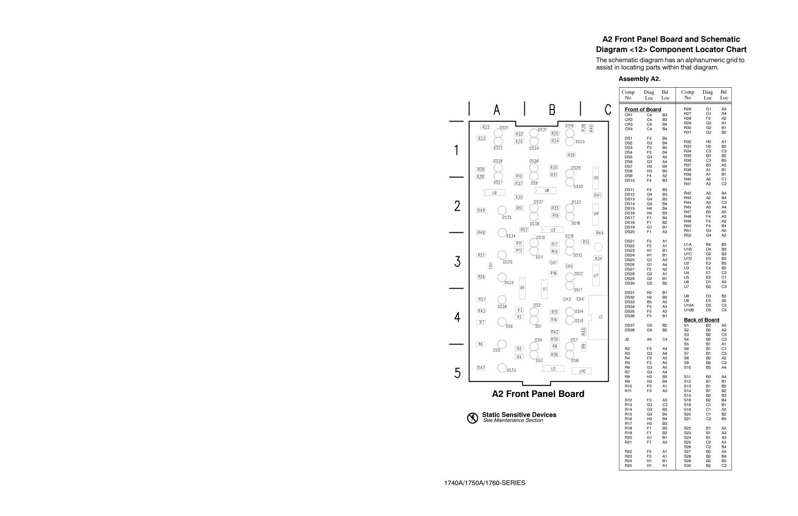
A2 Front Panel Board
Static Sensitive DevicesSee Maintenance Section
Front of Board
CR1 C4 B3
CR2 C4 B3CR3 C4 B4CR4 C4 B4
DS1 F3 B4
DS2 G3 B4DS3 F3 B5
DS4 F3 B4
DS5 G3 A5DS6 G3 A4
DS7 H3 B4DS8 H3 B5
DS9 F4 A2
DS10 F4 B3
DS11 F4 B3
DS12 G4 B3
DS13 G4 B3
DS14 G4 B4DS15 H4 B4
DS16 H4 B3
DS17 F1 B4
DS18 F1 B2
DS19 G1 B1DS20 F1 A3
DS21 F2 A1
DS22 F2 A1DS23 H1 B1
DS24 H1 B1
DS25 G1 A3
DS26 G1 A4
DS27 F2 A2DS28 G2 A1
DS29 G2 B1
DS30 G2 B2
DS31 H2 B1
DS32 H2 B2
DS33 B5 A5
DS34 F5 A3
DS35 F5 A2DS36 F5 B1
DS37 G5 B2
DS38 G5 B2
J2 A4 C4
R2 F3 A4
R3 G3 A4R4 F3 A5
R5 F3 A5
R6 G3 A5
R7 G3 A4R8 H3 B5
R9 H3 B4
R10 F3 A1
R11 F3 A3
R12 F3 A3
R13 G3 C3
R14 G3 B3
R15 G3 B4R16 H3 B4
R17 H3 B3
R18 F1 B3
R19 F1 B2
R20 G1 B1R21 F1 A3
R22 F2 A1
R23 F2 A1R24 H1 B1
R25 H1 A1
R26 G1 A3R27 G1 A4R28 F2 A2
R29 G2 A1
R30 G2 B1R31 G2 B2
R32 H2 A1
R33 H2 B2
R34 C3 C3R35 B3 B2
R36 C3 B5
R37 B3 A2
R38 A1 B1R39 A1 B1R40 A2 C1
R41 A2 C2
R42 A2 B4R43 A2 B4
R44 A3 C3
R45 A3 A4
R47 B5 A5R48 F4 A3
R49 F4 A2
R50 F4 B4
R51 G4 A2
R52 G4 A2
U1A B4 B3
U1B D4 B3
U1C D2 B3U1D E5 B3
U2 E3 B5
U3 E4 B2
U4 E1 C2
U5 E2 C1U6 D1 A3
U7 B3 C3
U8 D3 B2U9 E5 A2
U10A D5 C5
U10B D5 C5
Back of Board
S1 B2 A5
S2 B2 A3S3 B2 C5
S4 B2 C3
S5 B1 A1
S6 B1 C1
S7 B1 C3S8 B2 A2
S9 B2 C2
S10 B2 A4
S11 B3 A4
S12 B1 B1
S13 B1 B2
S14 B1 B2
S15 B2 B3S16 B2 B4
S18 C1 B1
S19 C1 A2
S20 C1 B2S21 C2 B5
S22 B1 A2
S23 B1 A3
S24 B1 A3S25 C2 A3
S26 C2 B4
S27 B5 A5
S28 B2 B4S29 B2 B5
S30 B2 C2
A2 Front Panel Board and Schematic
Diagram <12> Component Locator Chart
CompNo
The schematic diagram has an alphanumeric grid toassist in locating parts within that diagram.
DiagLoc
BdLoc
Assembly A2.
CompNo
DiagLoc
BdLoc
1740A/1750A/1760-SERIES

R2568.1
R2468.1
+5V1 +5V1
DS24
R2068.1
R2668.1
R2768.1
+5V1 +5V1 +5V1
DS19 DS25 DS26 DS23
R1868.1
R1968.1
R2168.1
+5V1 +5V1 +5V1
DS17 DS18 DS20
1760
VECTOR/SCHLED DRIVERS
1740A 1750A
SWITCH TEXT
SWITCH
S5
S18
WAVEFORM WAVEFORM
VECTOR VECTOR
WAVEFORM/AUDIO
MULTIPLE VECTOR/SCHPRESETWAVEFORM/
AUDIO
CURSOR
FILTER
BEZEL1
BEZEL4
PICTURE/
S5S24
S23 S6
S22 S7R4010.0K
R3910.0K
R3810.0K
+5V1
+5V1
+5V1
REF
BOWTIELIGHTNING/
CH A1/CH B1
CH A/CH B LINE/FIELD
S12 S18
S20S14
S13 S19
PB0
PB1
PB2
S20 SCH/AUDIOAUDIO LIGHTNING/BOWTIE
PB0
PB1
PB2
PB3
PB4
BMOSISER
10
A11
B12
C13
D14
E3
F4
G5
H6
CLK2
CLKINH15
SH/LD1
QH9
QH7
U674HC165
NC
BMOSI
BSCK
/LED_EN
/LED_CS
+5V1
SER14
QA15
QB1
SCLK11
QC2
SCLR10
QD3
QE4
RCLK12
QF5
G13
QG6
QH7
QH’9
U474HC595
LIN SELCH B1CH B3
R2268.1
R2368.1
R2868.1
+5V1 +5V1+5V1
CONFIGPRESETUNUSED(ALTMULT)
R2968.1
R3068.1
R3168.1
+5V1+5V1+5V1
SCHMULTIPLE
R3268.1
R3368.1
+5V1+5V1
VECTOR CH A1
DS32
CH A CH BAUDIO
DS31DS30DS29DS28
WAVEFORM PICTURE TIMECODE
DS27DS22DS21
BSCK
/LED_EN
/LED_CS
+5V1
SER14
QA15
QB1
SCLK11
QC2
SCLR10
QD3
QE4
RCLK12
QF5
G13
QG6
QH7
QH’9
U574HC595
PB5
PB6
PB7
BSCK
/PB_CS
/PB_ID_LD
MISO 98
10
U1C74HCT125
MAG
DC RESTRESTORE
EXTCH A2/CH B2
CH A3/CH B3
SEL A/SEL B
PARADE/
S26S28
S16 S25
S21S15PB3
PB4
PB5
LIN SEL
CRT
CLEARBEZEL5
BEZEL2
MENU
TIMECODE
S4S3
S2 S9
S8S1
R4310.0K
R4210.0K
R4110.0K
+5V1
+5V1
+5V1
CONFIG BEZEL3
GAIN
S11
S10 S30
R4510.0K
R4410.0K
+5V1
+5V1
OVERLAY
S29PB6
PB7
PB8
PB9
PB10
PB11
BMOSISER
10
A11
B12
C13
D14
E3
F4
G5
H6
CLK2
CLKINH15
SH/LD1
QH9
QH7
U874HC165
NC
BSCK
+5V1
SER14
QA15
QB1
SCLK11
QC2
SCLR10
QD3
QE4
RCLK12
QF5
G13
QG6
QH7
QH’9
U274HC595
EXTRESTORE(ALTEXT)UNUSED
R468.1
R568.1
R268.1
+5V1+5V1+5V1
DS1 DS4 DS3
GAINCRTUNUSED(ALTRESTORE)
R768.1
R668.1
R368.1
+5V1+5V1+5V1
DS2 DS5 DS6 DS7
OVERLAYPARADE
R868.1
R968.1
+5V1+5V1
DS8
SEL B CH A2
R1768.1
R1668.1
+5V1+5V1
DS16
CH A3 CH B2 SEL A
R1568.1
R1368.1
R1468.1
+5V1+5V1+5V1
DS15DS14DS13DS12
BOWTIE MAGUNUSED
R1068.1
R1168.1
R1268.1
+5V1+5V1+5V1
DS11DS10DS9
/LED_EN
/LED_CS
SER14
QA15
QB1
SCLK11
QC2
SCLR10
QD3
QE4
RCLK12
QF5
G13
QG6
QH7
QH’9
U374HC595
BSCK
/ID_CS
/PB_ID_LD
MISO 56
4
U1B74HCT125
R371.00K
R351.00K
R341.00K
R361.00K
23
CR1
23
CR2
PB8
PB9
/PB_CS
/ID_CS
/PB_ID_LD
/LED_CS
+5V1 +5V1 +5V1 +5V1
/FPAN_CS
/FPAN_EN
BMOSI
BSCK
+5V1
SER14
QA15
QB1
SCLK11
QC2
SCLR10
QD3
QE4
RCLK12
QF5
G13
QG6
QH7
QH’9
U774HC595
11
22
33
44
55
66
77
88
99
1010
J2
/FPAN_CS
/FPAN_EN
MISO 23
1
U1A74HCT125
23
CR3
23
CR4
PB10
PB11
/LED_CS
+5V1
BSCK
/LED_EN
/LED_CS
+5V1
(ALTMAG)
R5068.1
R4968.1
R4868.1
+5V1 +5V1 +5V1
LED 1740A
R5268.1
R5168.1
+5V1 +5V1
1750A
LED TEXT
1760
AUDIO
UNUSED
WAVEFORM
UNUSED
SCH
VECTOR
WAVEFORM
BOWTIE
SCH
AUDIO
VECTOR
LIGHTNING
LINE FIELD
DS9 AUDIO
DS21 UNUSED
DS24 VECTOR
DS28 WAVEFORM
DS31 UNUSED
DS36 UNUSED
DS37 DS38
CURSOR FILTER LIGHTNING
NC
NC
NC
DS34 DS35 DS36
BSCK
/LED_EN
/LED_CS
+5V1
SER14
QA15
QB1
SCLK11
QC2
SCLR10
QD3
QE4
RCLK12
QF5
G13
QG6
QH7
QH’9
U974HC595
NC
NC
NC
/LED_EN
/RESET
+5V1
+5V1
+5V1
D2
Q5
CK3
Q6
PR
4
CL
1
U10A74HC74
D12
Q9
CK11
Q8
PR
10
CL
13
U10B74HC74
/LED_CSON
NC
ON
POWER
POWER
S27
POWER_ON
MISO
BMOSI
BSCK
/RESET
VCC
+5V1+5V1
DS33
R4775.0
J2CONNECTS
TO J1
A3MAINBOARD
<11>
1740A/1750A/1760--SERIES
+5V1MISO 1211
13
U1D74HCT125
FRONT PANEL <12>
A2 FRONT PANEL BOARD

(with cross-references to Schematics 13, 14, 15, and 16)
A5 Vector Board Static Sensitive DevicesSee Maintenance Section
C32 D2 B3C42 F1 C2
C43 D2 C3
C45 F2 C3
C49 E2 C3
C68 B3 D3
C85 A3 E4
C102 B2 F4
C113 H1 C3C114 H1 C2
J1 H3 G1
L11 B2 F4
P1 A2 F4
Q13 C2 B3Q14 C3 C3
Q33 B1 G4
Q34 C1 G4
R73 C2 C3
R82 F1 C2
R83 F2 C2
R84 F2 C3
R85 C3 C3R86 C4 C4
R87 D4 C4
R89 C4 C4R90 C4 C4
R91 D4 C4
R92 D4 C4
R95 B4 C4
R114 D4 D3
R137 E4 E3
R138 F4 E3R139 F4 E4
R140 F4 E4
R150 C4 E3
R195 B2 F4R197 B2 F4
R209 C2 F4
R211 B1 G4
R212 C2 G4R213 H1 C3
R214 H1 C2
R215 G1 C3R216 G1 C3
U11B A4 B2
U11C A4 B2U11D C3 B2
U11E A5 B2
U11F B3 B2
U12A D2 C3
U12B C2 C3
U12C C3 C3
U12D D3 C3
U16 E1 C3U17A E1 C3
U17B E1 C3
U17C E5 C3U17D E5 C3
U18 F1 D2
U19 B4 D3
U21A E3 D3U21B F5 D3
U21C E4 D3
U21D B5 D3
U22 E2 D3U27 F4 E3
VR3 C1 G4
Schematic Diagram <13> Component Locator Chart
The schematic diagram has an alphanumeric grid to assist in locating parts within that diagram.
Assembly A5. Partial Assembly A5 also shown on Schematics 14, 15, and 16.
1740A/1750A/1760-SERIES
CompNo
DiagLoc
BdLoc
CompNo
DiagLoc
BdLoc
CompNo
DiagLoc
BdLoc
CompNo
DiagLoc
BdLoc
CompNo
DiagLoc
BdLoc
C1 16 E2 A1C2 16 F2 A2
C3 16 E1 A1
C4 16 F2 A2
C5 16 F4 A4C6 16 E2 A1
C7 16 G2 A3
C8 16 D5 A3C9 16 F4 A4
C10 16 G4 A3C11 16 D2 A2
C12 16 F3 A2
C13 16 D5 A3C14 16 F4 A3C15 16 E3 A4
C16 16 E4 A4C17 16 C3 B1
C18 16 F5 A2
C19 16 F3 A3C20 16 E3 A4
C21 16 C2 B1C22 16 C4 B3
C23 16 C4 B4C24 16 B2 B1C25 15 H2 B2
C26 16 B3 B2C27 16 E4 B2
C28 16 C4 B3C29 15 F5 B4
C30 16 D3 B2
C31 16 B1 B1
C32 13 D2 B3C33 15 H2 B1
C34 15 G5 B4
C35 15 H2 B1
C36 15 G2 C2
C37 15 G2 C1C38 15 G2 C2
C39 15 E5 C4
C40 15 G2 C1
C41 15 F1 C2C42 13 F1 C2
C43 13 D2 C3
C44 15 F1 C2
C45 13 F2 C3C46 15 D5 C4
C47 15 F3 C1
C48 15 D3 C2
C49 13 E2 C3
C50 15 E4 C2C51 15 F3 C1
C52 15 E3 C1
C53 15 F2 C1
C54 15 E3 C2C55 14 G1 D1
C56 15 F1 D2
C57 14 G2 D3
C58 14 G4 D2
C59 14 G4 D2C60 15 E2 D1C61 15 D2 D1
C62 15 D1 D1
C63 14 G1 F3C64 14 E2 D2
C65 14 H5 D2
C66 14 H4 D3
C67 14 G2 D3
C68 13 B3 D3C69 14 E2 D2
C70 14 G4 D3
C71 14 E4 D3
C72 14 F4 D3C73 14 F2 E2
C74 14 E4 E3
C75 15 B2 E1
C76 15 B3 E1
C77 15 C3 E1C78 * 14 G4 D2
C79 14 D2 E1
C80 14 F3 E2
C81 14 F4 E3C82 15 B3 E1
C83 15 B3 E1
C84 14 E3 E2
C85 13 A3 E4
C86 14 C3 E2C87 14 H3 E3
C88 14 C3 F3
C90 15 B2 F1
C91 15 B2 F1C92 14 C2 F2
C93 14 C2 F2
C94 14 A4 F1
C95 14 E5 F3
C96 15 B4 F1C97 14 C3 F2
C98 14 B4 F2C99 14 B4 F2
C100 14 B4 F2C101 14 C4 F3C102 13 B2 F4
C103 15 B4 F1
C104 14 A4 F2
C105 14 B3 F3C106 15 B4 F1C107 14 B3 F2
C108 14 C5 F4
C109 15 B4 G1C110 15 B5 G1
C111 15 B5 G1
C112 16 G2 A3
C113 13 H1 C3
C114 13 H1 C2C115 14 F1 D1
CR1 16 C4 B3CR2 15 F5 B4CR3 15 E5 C4
CR4 14 F2 D2
CR5 14 G3 D3
CR6 14 F2 D1
CR7 14 G2 E3CR8 15 B2 E1
CR9 15 C4 G1
CR10 14 E1 D1
J1 13 H3 G1
L1 16 B2 B1
L2 16 B2 C1
L3 15 H2 B1L4 15 G2 C1
L5 15 F1 C2
L6 14 E4 E3
L7 14 A4 F1L8 14 A4 F2
L9 14 C2 F2
L10 14 B5 F2
L11 13 B2 F4
P1 13 A2 F4
Q1 16 F3 A4
Q2 16 F1 A2Q3 16 F2 A2
Q4 16 F3 A4
Q5 16 C3 A1
Q6 16 C2 B1Q7 16 C5 B3
Q8 16 B4 B3
Q9 16 A4 B2
Q10 15 G2 B2
Q11 16 B4 B3Q12 16 B4 B3
Q13 13 C2 B3
Q14 13 C3 C3
Q15 14 F2 D2Q16 14 D1 D1
Q17 14 D1 E1
Q18 14 E3 E2
Q19 14 E3 E2
Q20 14 E3 E2Q21 14 F4 E3
Q22 14 C2 E2
Q23 15 A1 E2
Q24 14 B2 E3Q25 14 C2 F2
Q26 14 D4 F3
Q27 14 D4 F4
Q28 14 E4 F3
Q29 14 B4 F2Q30 14 A3 G2
Q31 14 C5 G3
Q32 14 C4 G3
Q33 13 B1 G4Q34 13 C1 G4
Q35 14 E1 D1
R1 16 F2 A2
R2 16 G2 A2R4 16 G2 A3
R5 16 G3 A3
R6 16 G4 A3
R7 16 F3 A4R8 16 F4 A4
R9 16 E2 A1
R10 16 E1 A1
R11 16 F2 A2
R12 16 G2 A3R13 16 G2 A3R14 16 G4 A3
R15 16 G4 A3
R16 16 F3 A4R17 16 E1 A1
R18 16 E1 A1R19 16 F2 A3
R20 16 F4 A3
R21 16 E3 A4R22 16 E1 A1
R23 16 E2 A2
R24 16 F2 A2
R25 16 F2 A2R26 16 F2 A2R27 16 F3 A4
R28 16 C3 A1
R29 16 E2 A2R31 16 C2 A1R32 16 D2 B1
R33 16 F4 A3
R35 16 D2 B1
R36 16 D2 B2R37 16 D2 B3
R38 16 D4 B3
R39 16 D4 B3
R40 16 D4 B3
R41 16 E3 B4R42 16 E4 B4
R43 16 E3 B4
R44 16 C2 B1
R45 16 C2 B1R46 16 D2 B3
R47 16 D4 B3
R48 16 E3 B4
R49 16 C4 B4
R50 16 D2 B2R51 16 E3 B2
R52 16 D4 B3
R53 16 C4 B3
R54 16 C4 B4R55 15 F5 B4
R56 16 D3 B2
R57 16 D3 B2
R58 16 E4 B3R59 16 B5 B3
R60 16 B4 B3
R61 15 F5 B4
R62 16 A3 B2
R63 16 D3 B2R64 16 B4 B3
R65 16 B4 B3
R66 16 B5 B3
R67 16 B4 B3R68 16 A4 B2
R69 15 G2 B2
R70 16 B4 C3
R71 15 G2 C1
R72 15 G2 C2R73 13 C2 C3
R74 15 G1 C1
R75 15 G2 C2
R76 15 E2 C1R77 15 E2 C1
R78 15 F1 C2
R79 15 F1 C3
R80 15 D5 C4
R81 15 D5 C4R82 13 F1 C2
R83 13 F2 C2
R84 13 F2 C3
R85 13 C3 C3R86 13 C4 C4
R87 13 D4 C4
R88 15 E3 C1
R89 13 C4 C4
R90 13 C4 C4R91 13 D4 C4
R92 13 D4 C4
R93 15 E3 C1
R94 15 F3 C1R95 13 B4 C4
R96 15 E3 D1
R97 15 F2 C1
R98 15 E3 C1
R99 15 E3 D1R100 15 E2 D1
R101 15 E2 D1
R102 14 G1 D2
R103 14 G5 D3R104 15 E3 D1
R105 15 E3 D1
R106 14 E2 D2
R107 14 G5 D2
R108 * 14 G4 D2R109 14 G4 D3R110 15 E3 D1
R111 15 E2 D1
R112 15 E2 D1R113 14 E2 D2
R114 13 D4 D3R115 15 D1 D1
R116 15 E1 D1
R117 15 E2 D1R118 14 G1 F3
R119 14 F2 D2
R120 14 G4 D3
R121 14 F2 D2R122 14 G3 D3R123 14 G3 D3
R124 14 D1 D1
R125 14 D1 D2R126 14 F2 D2R127 14 E2 D2
R128 14 D1 E1
R129 14 F3 E2
R130 14 E3 E2R131 14 D2 E2
R132 14 F4 D3
R133 14 D1 E2
R134 14 E3 E2
R135 14 G4 E2R136 14 D2 E3
R137 13 E4 E3
R138 13 F4 E3
R139 13 F4 E4R140 13 F4 E4
R141 15 C2 E1
R142 15 B3 E1
R143 14 D2 E2
R144 14 E3 E2R145 14 G4 E3
R146 15 C4 E1
R147 14 D1 E1
R148 14 C2 E2R149 14 F4 E3
R150 13 C4 E3
R151 15 B3 E1
R152 14 D2 E1R153 14 E3 E2
R154 15 A1 E2
R155 14 F4 E2
R156 14 H2 E3
R157 15 C3 E1R158 15 B2 E1
R159 15 A2 E2
R160 14 E3 E2
R161 14 E3 E2R162 14 B2 E3
R163 14 D3 E3
R164 15 B2 F1
R165 15 A2 F2
R166 14 C2 E2R167 14 B2 E2
R168 14 D4 E3
R169 15 C2 F1
R170 14 H3 F3R171 14 G2 F3
R174 15 B2 F1
R175 15 A2 F2
R176 14 B3 F2
R177 14 D5 F3R178 14 D4 F4
R179 14 B3 F3
R180 14 E4 F4
R182 14 B5 F2R183 14 A4 F2
R184 14 B4 F2
R185 14 B3 F2
R186 14 B3 F3
R187 14 B3 F3R188 14 B5 F3
R189 14 B5 F3
R190 14 D4 F3
R191 14 D4 F3R192 14 C4 F3
R193 14 C5 F4
R194 14 C5 F4
R195 13 B2 F4
R196 15 B4 F1R197 13 B2 F4
R198 15 B4 F1
R199 15 B5 F1
R200 14 A3 G2R201 14 A3 F2
R202 14 B3 F2
R203 14 B3 F2
R204 14 B4 F2
R205 14 B4 F2R206 14 C5 F3R207 14 C5 F3
R208 14 C4 F3
R209 13 C2 F4R210 15 B5 G1
R211 13 B1 G4R212 13 C2 G4
R213 13 H1 C3
R214 13 H1 C2R215 13 G1 C3
R216 13 G1 C3
R217 14 D1 D2
R218 14 E1 D1R219 14 E1 D1R220 14 E5 F3
T1 16 A1 B1
TP1 14 H3 D2
U1 16 G2 A2
U2 16 G4 A3U3A 16 C5 A1
U3B 16 C2 A1
U4A 16 F2 A2
U4B 16 G2 A2
U5A 16 D5 A3U5B 16 G4 A3
U5C 16 E5 A3
U5D 16 G2 A3
U6 16 D1 A2U7A 16 F4 A2
U7B 16 G4 A2
U8 16 D3 B3
U9 15 F5 B4
U10 15 D5 B4U11A 15 D3 B2
U11B 13 A4 B2
U11C 13 A4 B2
U11D 13 C3 B2U11E 13 A5 B2
U11F 13 B3 B2
U12A 13 D2 C3
U12B 13 C2 C3U12C 13 C3 C3
U12D 13 D3 C3
U13A 15 E4 C2
U13B 15 E2 C2
U13C 15 E2 C2U13D 15 E3 C2
U14 15 F3 C1
U15 15 F2 C1
U16 13 E1 C3U17A 13 E1 C3
U17B 13 E1 C3
U17C 13 E5 C3
U17D 13 E5 C3
U18 13 F1 D2U19 13 B4 D3
U20A 14 G2 D3
U20B 14 G4 D3
U20C 14 G5 D3U20D 14 F5 D3
U21A 13 E3 D3
U21B 13 F5 D3
U21C 13 E4 D3
U21D 13 B5 D3U22 13 E2 D3
U23A 14 E2 D2
U23B 14 E3 D2
U24A 14 G3 D2U24B 14 E2 D2
U25A 15 C2 D1
U25B 15 C3 D1
U26 14 F4 E3
U27 13 F4 E3U28A 14 G2 E3
U28B 14 G3 E3
U29A 15 B3 E1
U29B 15 B2 E1U29C 15 B2 E1
U30 14 C3 F2
U31 14 D4 F3
VR1 14 G1 D2VR2 14 G1 F4
VR3 13 C1 G4
Y1 15 B4 F1Y2 15 B5 F2
A5 Vector Board Component Locator ChartCompNo
DiagNo
DiagLoc
BdLoc
CompNo
DiagNo
DiagLoc
BdLoc
CompNo
DiagNo
DiagLoc
BdLoc
CompNo
DiagNo
DiagLoc
BdLoc
CompNo
DiagNo
DiagLoc
BdLoc
*See Parts List
for earlier serial
number ranges.

DAC
SDO4
VOUT014
VOUT115
VOUT216
VOUT317
VOUT418
VOUT519
VOUT620
VOUT721
VOUT823
VOUT924
VOUT1025
VOUT1126
VOUT1227
VOUT1328
VOUT141
VOUT152
SDI8
VREFOUT11
VREFIN12
SCLK7
LD6
16/4 MODE5
RBIAS10
VDD3
DGND9
AGND22
VSS13
U18I10412
56
4
U17B74HCT125
MISO
CHROMAAMP
R2113.92K
R21210.0K
Q34
Q33
REF_CHROMA
+8V
+8V
3
2
VR3
A5
2 3
1U17A
74HCT125/DAC_CS
/DAC_LD
BMOSI
BSCK
---8V
GND5
IN2
IN3
IN6
IN7
OUT1
U1679L05
NC
NC
C42.1UF
R8210.0K
+5V
+5V
<15>
<15>
<15>
<15> D2
D3
D4
D2
R215100.0K
C113.1UF
C114.1UF
R216100.0K
B_COSINE
A_COSINE
A_SINE
B_SINE
REF_CAL
DOT_CAL<16>
<16>
F2
F4
R21410.0K
R21310.0K
RY_OFFSET
BY_OFFSET
NC
NC
NC
NC
NC
B2
R831.00M
R841.00M
C45.1UF
SCH_GAIN
8 BIT SERIAL OUTPUT
C49.1UF
<14>
C43.1UF
2 3
1
12
13
45
U12ADG444
+8V
+5V
Q13
7 6
8
U12BDG444
R1951.82K
R1975.62K
R2091.82K
---8V
---8V
C102100PF
L1115UH
INT_VIDEO
REF_VIDEO
VEC_CHROM+
SCH_SIG
1A1
1B2
2A3
2B4
3A5
3B6
4A7
4B8
5A9
5B10
6A11
6B12
7A13
7B14
8A15
8B16
9A17
9B18
10A19
10B20
11A21
11B22
12A23
12B24
13A25
13B26
14A27
14B28
15A29
15B30
16A31
16B32
17A33
17B34
P1
P1CONNECTS
TO J9
<7>
A3MAINBOARD
<16>
<16>
H4
H2
C8522UF
R---Y
B---Y
SCH_FIELD
VEC_SCH_SW
---11V
+5V
+5V
+11V
<16>
F3
R7322.1K
10 11
9
U12CDG444
9 8
U11D74HCT04DEMOD_CLMP
VEC_SCH_SW
VEC_CHROM+
<16>
B4
R8522.1K
1514
16
U12DDG444
Q14
C32.1UF
CHROMA
---8V SER14
QA15
QB1
SCLK11
QC2
SCLR10
QD3
QE4
RCLK12
QF5
G13
QG6
QH7
QH’9
U2274HC595
BMOSI
BSCK
/WRITE_CS
+5V
NC
NC
<16>
<15>
A2
A3 B4
+V
NTSC
/TEST
INT/EXT
/NTSC
PAL1/4
<15> <16><14> F3 B5
A4
/NTSC
REF_VIDEO
INT_VIDEO
<15><14>
1A1
1B2
2A3
2B4
3A5
3B6
4A7
4B8
5A9
5B10
6A11
6B12
7A13
7B14
8A15
8B16
9A17
9B18
10A19
10B20
11A21
11B22
12A23
12B24
13A25
13B26
14A27
14B28
15A29
15B30
16A31
16B32
17A33
17B34
J1
J1CONNECTS
TO J1NC
<14>H3Q
DOT_CAL
REF_CAL
BURST_GATE
ST_SAMPLE
INT/EXT
SYNC_GATE
/NTSC
ODD_FIELD
PAL1/4
VEC_SCH_SW
SER10
A11
B12
C13
D14
E3
F4
G5
H6
CLK2
CLKINH15
SH/LD1
QH9
QH7
U2774HC165
R14010.0K
R13910.0K
R13810.0K
+5V+5V+5V
SCH BOARD ID
R13710.0K
23
1
U21A74HCT125
MISO
BMOSI
+5V
<14>
B2
G3 B3
BURST_GATE
/BLANK_CK <16><14>
A4<16>
<15> D4
13 12
U11F74HCT04
C68100PF
R9510.0K
A/B
CHROM_GATE
MISO
BURST_GATE
ST_SAMPLE
SYNC_GATE
/VEC_CS
/VEC_EN
BLANK_CK
ODD_FIELD
BMOSI
+5V
NC
NC5 6
U11C74HCT04
3 4
U11B74HCT04
BMOSI
BSCK
BSCK
SERIAL ADDRESS DEMUX
SER14
QA15
QB1
SCLK11
QC2
SCLR10
QD3
QE4
RCLK12
QF5
G13
QG6
QH7
QH’9
U1974HC595
R8910.0K
R9010.0K
R15010.0K
+5V+5V+5V
+5V
R8710.0K
R11410.0K
R9110.0K
R9210.0K
R8610.0K
/ID_CS
/ID_LD
/DAC_CS
/DAC_LD
+5V+5V+5V+5V+5V
<14>
G3 9 8
10
U21C74HCT125
LOCKED
SCH_ID_1
SCH_ID_0
SCH_ID_2
SCH_ID_3
BSCK
56
4
U21B74HCT125
/ID_CS
MISO
/ID_LD
BSCK
SCH_ID_2
SCH_ID_1
SCH_ID_0
SCH_ID_3
SCH_FIELD
SCH_LOCKED
A6
BOARD
<17>
SCH
NC
---8V
+5V
+8V
SCH_SIG
SCH_GAINMISO
MISO
MISO<14>
F1
9 8
10
U17C74HCT125
12 11
13
U17D74HCT125
BRST_PRSNT
/SCH_LK_RD
/VEC_LK_RD
SCH_LOCKED
/BRST_RD
/WRITE_CS
/VEC_LK_RD
/SCH_LK_RD
/BRST_RD
1211
13
U21D74HCT125
NC11 10
U11E74HCT04
MISO
/VEC_CS
/VEC_EN
1740A/1750A/1760--SERIES DACS & DIGITAL CONTROL <13>
PART OF A5 VECTOR BOARD

C55 G1 D1C57 G2 D3C58 G4 D2
C59 G4 D2
C63 G1 F3
C64 E2 D2C65 H5 D2
C66 H4 D3C67 G2 D3C69 E2 D2
C70 G4 D3
C71 E4 D3C72 F4 D3
C73 F2 E2
C74 E4 E3
C78 * G4 D2C79 D2 E1
C80 F3 E2
C81 F4 E3
C84 E3 E2
C86 C3 E2
C87 H3 E3
C88 C3 F3
C92 C2 F2C93 C2 F2
C94 A4 F1
C95 E5 F3C97 C3 F2
C98 B4 F2
C99 B4 F2
C100 B4 F2C101 C4 F3
C104 A4 F2
C105 B3 F3
C107 B3 F2
C108 C5 F4
C115 F1 D1
CR4 F2 D2CR5 G3 D3
CR6 F2 D1
CR7 G2 E3
CR10 E1 D1
L6 E4 E3
L7 A4 F1
L8 A4 F2L9 C2 F2
L10 B5 F2
Q15 F2 D2
Q16 D1 D1Q17 D1 E1
Q18 E3 E2
Q19 E3 E2
Q20 E3 E2
Q21 F4 E3Q22 C2 E2
Q24 B2 E3
Q25 C2 F2
Q26 D4 F3
Q27 D4 F4
Q28 E4 F3
Q29 B4 F2
Q30 A3 G2
Q31 C5 G3
Q32 C4 G3
Q35 E1 D1
R102 G1 D2
R103 G5 D3
R106 E2 D2
R107 G5 D2R108 * G4 D2
R109 G4 D3
R113 E2 D2R118 G1 F3
R119 F2 D2
R120 G4 D3
R121 F2 D2R122 G3 D3
R123 G3 D3
R124 D1 D1
R125 D1 D2
R126 F2 D2
R127 E2 D2
R128 D1 E1
R129 F3 E2R130 E3 E2
R131 D2 E2
R132 F4 D3R133 D1 E2R134 E3 E2
R135 G4 E2
R136 D2 E3R143 D2 E2
R144 E3 E2
R145 G4 E3
R147 D1 E1
R148 C2 E2
R149 F4 E3
R152 D2 E1R153 E3 E2
R155 F4 E2
R156 H2 E3
R160 E3 E2R161 E3 E2
R162 B2 E3
R163 D3 E3
R166 C2 E2R167 B2 E2
R168 D4 E3
R170 H3 F3R171 G2 F3
R176 B3 F2
R177 D5 F3
R178 D4 F4
R179 B3 F3R180 E4 F4
R182 B5 F2
R183 A4 F2R184 B4 F2
R185 B3 F2
R186 B3 F3
R187 B3 F3R188 B5 F3
R189 B5 F3
R190 D4 F3
R191 D4 F3
R192 C4 F3
R193 C5 F4
R194 C5 F4
R200 A3 G2R201 A3 F2
R202 B3 F2
R203 B3 F2R204 B4 F2
R205 B4 F2
R206 C5 F3
R207 C5 F3R208 C4 F3
R217 D1 D2
R218 E1 D1
R219 E1 D1R220 E5 F3
TP1 H3 D2
U20A G2 D3U20B G4 D3
U20C G5 D3
U20D F5 D3
U23A E2 D2
U23B E3 D2
U24A G3 D2
U24B E2 D2U26 F4 E3
U28A G2 E3
U28B G3 E3
U30 C3 F2U31 D4 F3
VR1 G1 D2
VR2 G1 F4
Schematic Diagram <14> Component Locator Chart
The schematic diagram has an alphanumeric grid toassist in locating parts within that diagram.
Assembly A5. Partial Assembly A5 also shown onSchematics 13, 15, and 16.
CompNo
DiagLoc
BdLoc
CompNo
DiagLoc
BdLoc
CompNo
DiagLoc
BdLoc
1740A/1750A/1760-SERIES
* See Parts List for earlier serial number ranges.

1740A/1750A/1760--SERIES

C25 H2 B2C29 F5 B4C33 H2 B1
C34 G5 B4
C35 H2 B1
C36 G2 C2C37 G2 C1
C38 G2 C2C39 E5 C4C40 G2 C1
C41 F1 C2
C44 F1 C2C46 D5 C4
C47 F3 C1
C48 D3 C2
C50 E4 C2C51 F3 C1
C52 E3 C1
C53 F2 C1
C54 E3 C2
C56 F1 D2
C60 E2 D1
C61 D2 D1
C62 D1 D1C75 B2 E1
C76 B3 E1
C77 C3 E1C82 B3 E1
C83 B3 E1
C90 B2 F1
C91 B2 F1C96 B4 F1
C103 B4 F1
C106 B4 F1
C109 B4 G1
C110 B5 G1
C111 B5 G1
CR2 F5 B4CR3 E5 C4CR8 B2 E1
CR9 C4 G1
L3 H2 B1
L4 G2 C1L5 F1 C2
Q10 G2 B2Q23 A1 E2
R55 F5 B4
R61 F5 B4R69 G2 B2
R71 G2 C1
R72 G2 C2
R74 G1 C1R75 G2 C2
R76 E2 C1
R77 E2 C1
R78 F1 C2
R79 F1 C3
R80 D5 C4
R81 D5 C4
R88 E3 C1R93 E3 C1
R94 F3 C1
R96 E3 D1R97 F2 C1
R98 E3 C1
R99 E3 D1
R100 E2 D1R101 E2 D1
R104 E3 D1
R105 E3 D1
R110 E3 D1
R111 E2 D1
R112 E2 D1
R115 D1 D1R116 E1 D1
R117 E2 D1
R141 C2 E1R142 B3 E1R146 C4 E1
R151 B3 E1R154 A1 E2
R157 C3 E1
R158 B2 E1
R159 A2 E2
R164 B2 F1R165 A2 F2
R169 C2 F1
R174 B2 F1
R175 A2 F2R196 B4 F1
R198 B4 F1
R199 B5 F1R210 B5 G1
U9 F5 B4
U10 D5 B4
U11A D3 B2U13A E4 C2
U13B E2 C2
U13C E2 C2U13D E3 C2
U14 F3 C1
U15 F2 C1
U25A C2 D1
U25B C3 D1
U29A B3 E1
U29B B2 E1
U29C B2 E1
Y1 B4 F1
Y2 B5 F2
Schematic Diagram <15> Component Locator Chart
The schematic diagram has an alphanumeric grid toassist in locating parts within that diagram.
Assembly A5. Partial Assembly A5 also shown onSchematics 13, 14, and 16.
CompNo
DiagLoc
BdLoc
CompNo
DiagLoc
BdLoc
CompNo
DiagLoc
BdLoc
1740A/1750A/1760-SERIES

<13>
F3
/TEST Q23
R1592.21K
R15410.0K +5V
+5V
NCSET
7Q
3
Q4
RST5
CLK12
CE8
D9
VEE10
VCC220
VCC12
U25AMC10H131
R169562.0
VCXO
R11510.0 C62
.1UF
+5V
R116562.0 R111
100.0
R112100.0
C56.1UF
612
8
10
4
U151496
L515UH
R78681.0
C4110PF
C441UF
R79100.0
+8V
+8V
R741.50KC40
.1UF
+8V
<16>
A2
C25120PF
C3333PF
SUBC
Q10
R72100.0
R6947.5K
C3833PF
R7511.0K
L468UH
C371000PF
R71100.0
L35.6UH
C35250PF
---8V
R776.81K
1
5 2
3
14
C53.1UF
R972.74K
C3682PF
---8V
R117562.0
10 11
9
U13CDG444
7 6
8
U13BDG444
R76681.0
R100100.0
C60470PF
R1012.21K
<13>
<13>
<14>
A4 G1
G1
C61.1UF
FSC
B_COSINE
A_COSINE
A/B
+5V
NC
NC
NC
R141562.0
C91.1UF
R158562.0
C7510PF
R164562.0
15
17
18
19
U29CMC10116
12
13
8
9
U29BMC10116
NC
CR8
R17510.0K
R16510.0K
C90150PF
R1741.82K
<14>
H4
ERROR
NC
NC
NC
NC
SET15
Q19
Q18
RST17
CLK12
CE14
D13
U25BMC10H131
C7782PF
R15110.0
C82.1UF
C76.1UF
+5V
5
7
3
4
2 20
10
14
U29AMC10116
G1
1 2
U11A74HCT04
A/B
R110562.0
R104562.0
R99100.0
R105100.0
R93681.0
1
5 2
3
14
R942.74K
612
8
10
4
U141496
C47.1UF
+8V
R886.81K
C51.1UF---8V
C48.1UF
15 14
16
U13DDG444
2 3
1
12
13
45
U13ADG444
C54.1UF
C50.1UF
C52470PF
R96100.0
R982.21K
+8V
+5V
<13>
<13>
A3
G1
B_SINE
A_SINE
PALNETTING
R157562.0
2
13
CR9C9682PF
R14210.0K
C83470PF
C1064.5---20PF
Y117.734MHZ
---8V
<13>
F3R198562.0
C1094.5---20PF
Y214.31818MHZ
NTSC
NETTINGNTSC
C103.1UF
R196562.0
R1461.00K
C111160PF
<13>
--8V SUPPLY
A/B
---8V
+8V SUPPLY
R61NOT INSTALLED
+8V
21
3
CR2
IN1
OUT3
G
2
U97808ACT
C29.1UF
C34220UF
+11V
R55NOT INSTALLED
R81NOT INSTALLED
R80NOT INSTALLED
C39220UF
---8V
2 1
3
CR3
IN2
OUT3G
1
U107908ACT
C46.1UF
---11VC110.1UF
R210562.0
<13>
G3R199562.0
/NTSC
1740A/1750A/1760--SERIES
NOTE:
PHASE SHIFTER <15>
AND SERIAL NUMBER RANGES.SEE PARTS LIST FOR EARLIER VALUES
PART OF A5 VECTOR BOARD

C1 E2 A1C2 F2 A2C3 E1 A1
C4 F2 A2
C5 F4 A4
C6 E2 A1C7 G2 A3
C8 D5 A3C9 F4 A4C10 G4 A3
C11 D2 A2
C12 F3 A2C13 D5 A3
C14 F4 A3
C15 E3 A4
C16 E4 A4C17 C3 B1
C18 F5 A2
C19 F3 A3
C20 E3 A4
C21 C2 B1
C22 C4 B3
C23 C4 B4
C24 B2 B1C26 B3 B2
C27 E4 B2
C28 C4 B3C30 D3 B2
C31 B1 B1
C112 G2 A3
CR1 C4 B3
L1 B2 B1
L2 B2 C1
Q1 F3 A4Q2 F1 A2
Q3 F2 A2
Q4 F3 A4
Q5 C3 A1
Q6 C2 B1
Q7 C5 B3
Q8 B4 B3
Q9 A4 B2Q11 B4 B3
Q12 B4 B3
R1 F2 A2R2 G2 A2
R4 G2 A3
R5 G3 A3
R6 G4 A3
R7 F3 A4
R8 F4 A4
R9 E2 A1
R10 E1 A1R11 F2 A2
R12 G2 A3
R13 G2 A3
R14 G4 A3R15 G4 A3
R16 F3 A4
R17 E1 A1R18 E1 A1
R19 F2 A3
R20 F4 A3
R21 E3 A4
R22 E1 A1
R23 E2 A2
R24 F2 A2
R25 F2 A2R26 F2 A2
R27 F3 A4
R28 C3 A1
R29 E2 A2R31 C2 A1
R32 D2 B1
R33 F4 A3R35 D2 B1
R36 D2 B2
R37 D2 B3
R38 D4 B3
R39 D4 B3
R40 D4 B3
R41 E3 B4
R42 E4 B4
R43 E3 B4
R44 C2 B1
R45 C2 B1
R46 D2 B3R47 D4 B3
R48 E3 B4
R49 C4 B4
R50 D2 B2R51 E3 B2
R52 D4 B3
R53 C4 B3
R54 C4 B4
R56 D3 B2
R57 D3 B2
R58 E4 B3
R59 B5 B3
R60 B4 B3
R62 A3 B2
R63 D3 B2R64 B4 B3
R65 B4 B3
R66 B5 B3
R67 B4 B3R68 A4 B2
R70 B4 C3
T1 A1 B1
U1 G2 A2
U2 G4 A3
U3A C5 A1
U3B C2 A1U4A F2 A2
U4B G2 A2
U5A D5 A3U5B G4 A3
U5C E5 A3
U5D G2 A3
U6 D1 A2U7A F4 A2
U7B G4 A2
U8 D3 B3
Schematic Diagram <16> Component Locator Chart
The schematic diagram has an alphanumeric grid toassist in locating parts within that diagram.
Assembly A5. Partial Assembly A5 also shown onSchematics 13, 14, and 15.
CompNo
DiagLoc
BdLoc
CompNo
DiagLoc
BdLoc
CompNo
DiagLoc
BdLoc
1740A/1750A/1760-SERIES

<15>
H2 L182UH
1
4
2
5
3
6
T1
SUBC
C31100PF
R45392.0
R44392.0
R32100.0
R35100.0
8
10
1
4
6
12
5
2 314
U61496
CHROMINANCE
DEMODULATORSR2210.0
R23100.0
C3100UF
R171.50K R10
1.00KR18100.0
C1120PF
+8V
Q2
R111.00K
R24100.0
R251.00K
Q3
+8V
+8V
DEMODULATOR OUTPUT
FILTERS & AMPLIFIERS
R133.92K
+8V
+8V
<13>
A2
R---Y
NC
R21.00K
C7.1UF
R42.21K
3
2
1 8
6
7
4
U1LM6361
R123.32K
C11215PF
---8V
<13>
H1
R262.21K
C4100PF
C2220PFR1
1.00K
RY_OFFSET
+8V
C11.1UF
C6150PF
R95.62K
---8V
+8V
+VBAL
R46100.0
R37100.0
R50100.0K
C21.1UF
R361K
---8V
+5V
SWITCHER
V--AXIS
R341.00M
Q6D12
Q9
CK11
Q8
PR
10
CL
13
U3B74HCT74
R31392.0
+V
PAL QUAD PHASE
<13>
F2
H2
C2416.8PF
L211.2---16.8UH
<13>
<14>
B3
R301.00M
Q5
R28392.0
D
/BLANK_CK
+5V
C17.1UF
+5V
R4810.0
R293.32K
+8V
R--Y CENTER DOT
POSITION CLAMP
<13>
B3
3
21
8
4
U4AMC34002
C19.1UF
R1922.1K
C12.1UF
DEMOD_CLMP
---8V
15 14
16
U5DDG444
5
67
U4BMC34002
<13>
A2
B---Y
NC
R151.00K
R53.92KC10
.1UF
R62.21K
3
2
1 8
6
7
4
U2LM6361
+8V
+8V
---8V
Q1
R161.00K
R71.00K
C9100PF
C5220PF
R27100.0
Q4
R81.00K
R202.21K
+8V
+8V
C20120PF
R51100.0
R521.00K
C27.1UF
8
10
1
4
6
12
5
2 314
U81496
C15100UF
R411.50K R43
1.00KR21100.0
R425.62K
C16150PF
+8V
R40475.0
R38100.0
R57100.0
R63100.0
C30.1UF
R56392.0
Q12
C22.01UF
QUADPHASE
NTSC
<13>
D2
R621.00M
Q9
R6810.0K
CHROMA
+8V
C264.5---20PF
<13>
F3
NTSC
<13>
A3 Q8
R672.21K
R604.75K
CHROM_GATE
+5V
+5V
NC
R5310.0K
2 1
3
CR1
R6447.5K
Q11
R702.21K
R6533.2K
C28.1UF
+8V
---8V
C23.1UF
R541.82K
R47100.0
R491.50K R39
475.0
---8V
R583.32K
---8V
B--Y CENTER DOT
<13>
H1
3
21
8
4
U7AMC34002
C14.1UF
R3322.1K
BY_OFFSET
+8V
---8V
R143.32K
5
67
U7BMC34002
7 6
8
U5BDG444
C18.1UF
NC NC
C8.1UF
C13.1UF
10 11
9
U5CDG444
+8V
---8V
POSITION CLAMP
NC
NC
NC
D2
Q5
CK3
Q6
PR
4
CL
1
U3A74HCT74
2 3
1
12
13
45U5A
DG444
+5V
NC
NC
Q7
R5947.5K
---8V
R6610.0K
---8V
1740A/1750A/1760--SERIES
NOTE:
DEMODULATOR <16>
AND SERIAL NUMBER RANGES.SEE PARTS LIST FOR EARLIER VALUES
PART OF A5 VECTOR BOARD

A6 SCH BoardStatic Sensitive DevicesSee Maintenance Section
C3 D1 A4C5 E1 A4
C9 A2 A3
C10 D1 A4C16 B1 B3C17 E1 B3
C19 B3 B4
C20 B3 B4
C23 B2 B3
C24 E1 B3
C26 E1 C4
C27 B1 B3
C28 B4 F4C30 D1 C3
C31 A2 A3
C32 D3 D3
C33 E3 C4
C34 E3 D4C35 E3 D4
C36 F4 F3
C37 D3 D3C38 E3 D4
C39 D4 F4
C42 D3 D3
C46 D3 D3
C47 E2 D4C49 D3 E3
C56 C3 F3
C57 E1 F2
C59 C3 E3
C66 E1 F3
C67 E1 G4C70 E4 F3
C71 E4 F3
C75 G1 D3
C77 H1 E3C80 H1 D2
C81 F5 D4
C85 D1 C2
C86 E1 B2
C87 D1 F3C88 E1 E3
C89 H1 E2
C90 * D4 F4
CR1 D3 E3
CR2 D3 C3
CR7 C2 C2
CR8 C2 C2
CR10(D1) D3 D4
J1 A3 A1
L3 B2 B4L6 H1 D3
Q8 A2 A3
Q9 A1 A4
Q10 A1 B3Q12 B1 B3
Q13 B3 B3
Q15 C4 E4
Q19 G3 F2Q20 F3 F3
Q21 G1 D2
Q22 G1 D2Q26 F5 G4
Q27 G2 D3
Q28 B1 A4
Q29 H2 D2
R13 B4 A3
R14 B4 A3
R15 B4 A3
R21 B4 A4R26 A2 A3
R27 A1 A3
R28 B1 A3
R34 A2 A3R35 A2 A3
R36 B2 B3
R37 A1 A3
R38 A1 A3R39 B3 B4
R42 B2 B3
R45 C1 B3
R46 C1 B3R48 B4 E4
R50 C2 C3
R51 C2 C3
R54 C4 E4
R57 D2 E4
R60 E3 C4
R61 F4 F3
R62 D4 E4R68 E2 D4
R69 E3 D4
R76 E3 E4R87 D3 E4
R88 E3 D4
R96 D3 E3
R100 D3 F3
R101 D3 E3
R102 E3 E4
R107 C3 E3
R108 C3 F3R112 F3 F3
R113 G3 F3
R114 B2 F3
R117 G4 F3R122 E4 F3
R123 G4 F3
R124 G4 G3
R125 G4 F3R131 G5 F3
R132 F4 G3
R133 F4 G3
R134 G5 F4R135 G5 F4
R139 G1 C2
R140 G2 D2
R141 G2 D2R143 G1 D2
R144 H1 D2
R145 G2 D2
R146 H1 E3R150 H3 F3
R153 G5 G3
R154 F5 C4R155 F5 C4
R156 D4 E3
R157 E5 C4R163 E5 C3
R164 D5 C3
R165 D5 C3
R167 G1 B2
R168 H1 F3R170 H2 D2
R171 G3 D3
R172 F2 E3
R173 C1 C3
R174 B1 A4
R175 B2 A4
R176 A2 A4
R177 C1 C3R178 B4 F4
R179 C4 F4
R180 C4 F4
R181 B2 B3R182 H1 D2
R183 H2 D2
R184 H2 D2
R185 D2 D1
R186 D2 D1
TP1 E5 D2
U4 B1 B3U7 B2 B3
U9 G1 C2
U10A C4 E4U10B C4 E4
U11A E3 C4
U11B E3 C4
U11C E2 C4U12A D4 F4
U12B F4 F4
U13C H3 D1
U14A E5 E2U23A G4 G3
U23B G4 G3
U23C H4 G3
U23D G4 G3U25 H1 E3
U27A C3 C3
U27B C3 C3
U28A E5 C4
U28B E5 C4
U29 C1 B2
U30 F3 E3
U32 B5 B2U33 B5 B3
U34 C5 F4
U35A G2 D2
U35B C2 D2
Y1 D3 D3
Y2 D3 D3
Schematic Diagram <17> Component Locator ChartThe schematic diagram has an alphanumeric grid to assist in locating parts within that diagram.
Assembly A6. Partial Assembly A6 also shown on Schematic 18.
1740A/1750A/1760-SERIES
CompNo
DiagLoc
BdLoc
CompNo
DiagLoc
BdLoc
CompNo
DiagLoc
BdLoc
CompNo
DiagLoc
BdLoc
CompNo
DiagLoc
BdLoc
C1 18 A1 A1C2 18 A5 A1
C3 17 D1 A4
C4 18 C1 A1C5 17 E1 A4C6 18 C1 A1
C7 18 C4 A2
C8 18 B5 A2
C9 17 A2 A3C10 17 D1 A4
C11 18 B1 A1C12 18 C1 B1
C13 18 B5 B2C14 18 C4 B1
C15 18 B2 B1
C16 17 B1 B3
C17 17 E1 B3
C18 18 C3 B2C19 17 B3 B4
C20 17 B3 B4
C21 18 C4 C1C22 18 B2 C1
C23 17 B2 B3
C24 17 E1 B3
C25 18 E4 C1
C26 17 E1 C4C27 17 B1 B3
C28 17 B4 F4
C29 18 D4 C2
C30 17 D1 C3
C31 17 A2 A3
C32 17 D3 D3
C33 17 E3 C4
C34 17 E3 D4C35 17 E3 D4
C36 17 F4 F3
C37 17 D3 D3
C38 17 E3 D4C39 17 D4 F4
C40 18 E3 E1
C41 18 E4 D1C42 17 D3 D3
C43 18 B2 E4
C44 18 F2 E2
C45 18 F2 E2
C46 17 D3 D3C47 17 E2 D4
C48 18 G2 E2
C49 17 D3 E3
C51 18 B2 F2
C52 18 D1 E1
C53 18 D2 E2
C54 18 C2 E1
C55 18 D2 E2C56 17 C3 F3
C57 17 E1 F2
C59 17 C3 E3
C60 18 D2 F1C61 18 E2 F2
C62 18 D2 F2
C64 18 E2 F2
C65 18 G1 F2C66 17 E1 F3
C67 17 E1 G4
C69 18 E2 F1
C70 17 E4 F3C71 17 E4 F3
C72 18 H1 G3
C73 18 G3 A4C74 18 H3 B4
C75 17 G1 D3
C77 17 H1 E3C80 17 H1 D2
C81 17 F5 D4C83 18 D5 C1
C84 18 D5 B1
C85 17 D1 C2C86 17 E1 B2
C87 17 D1 F3
C88 17 E1 E3
C89 17 H1 E2C90 17 D4 F4C91 18 G4 G3
CR1 17 D3 E3
CR2 17 D3 C3CR3 18 E2 F2
CR4 18 E2 F1
CR5 18 F2 G1
CR6 18 F2 G1CR7 17 C2 C2
CR8 17 C2 C2
CR9 18 F4 G2
CR10(D1) 17 D3 D4
J1 17 A3 A1
L1 18 B5 B2
L2 18 C1 B1L3 17 B2 B4
L4 18 D1 F2
L5 18 D1 E2
L6 17 H1 D3
Q1 18 C2 A1
Q2 18 B1 A1
Q3 18 B4 A2
Q4 18 A4 A2Q5 18 B1 B1
Q6 18 B5 A2
Q7 18 B5 A2
Q8 17 A2 A3Q9 17 A1 A4
Q10 17 A1 B3
Q11 18 B4 B1
Q12 17 B1 B3Q13 17 B3 B3
Q14 18 D3 B2
Q15 17 C4 E4
Q16 18 F3 C1Q17 18 E3 D1
Q19 17 G3 F2
Q20 17 F3 F3
Q21 17 G1 D2
Q22 17 G1 D2
Q26 17 F5 G4
Q27 17 G2 D3
Q28 17 B1 A4Q29 17 H2 D2
R1 18 B2 A1
R2 18 A1 A1
R4 18 B1 A1R5 18 B1 A1
R6 18 B4 A1
R7 18 B4 A1
R8 18 A5 A2R9 18 A4 A2
R13 17 B4 A3
R14 17 B4 A3
R15 17 B4 A3R16 18 B4 A1
R17 18 C4 A1R18 18 B5 A2R19 18 B5 A2
R21 17 B4 A4
R22 18 B1 A1
R23 18 B1 A1R24 18 B1 B2R25 18 C4 A2
R26 17 A2 A3R27 17 A1 A3
R28 17 B1 A3R29 18 C4 B2
R30 18 B5 B2R31 18 B5 B2R32 18 C4 B2
R33 18 A5 A2
R34 17 A2 A3
R35 17 A2 A3
R36 17 B2 B3
R37 17 A1 A3
R38 17 A1 A3
R39 17 B3 B4R40 18 C3 B2
R42 17 B2 B3
R43 18 D3 B2
R44 18 D3 C2R45 17 C1 B3
R46 17 C1 B3
R48 17 B4 E4
R50 17 C2 C3R51 17 C2 C3
R54 17 C4 E4
R55 18 F3 C1
R57 17 D2 E4R58 18 E3 C1
R59 18 E4 C1
R60 17 E3 C4
R61 17 F4 F3
R62 17 D4 E4
R63 18 E4 D1
R64 18 E5 D1
R65 18 E3 C2R66 18 E4 D2
R67 18 E4 C2
R68 17 E2 D4
R69 17 E3 D4R70 18 F5 D1
R71 18 F4 D1
R72 18 F4 D1
R73 18 E4 E1R74 18 E5 D1
R76 17 E3 E4
R78 18 E4 E1
R79 18 D3 E1R80 18 F2 E2
R81 18 F3 E1
R82 18 F2 E2
R83 18 G2 E2
R84 18 F1 D2
R85 18 F2 E2
R87 17 D3 E4
R88 17 E3 D4R89 18 F1 E2
R90 18 E3 E1
R91 18 G1 E2R92 18 E3 E1
R93 18 G1 E2R94 18 G1 E2
R95 18 G2 E2R96 17 D3 E3
R100 17 D3 F3
R101 17 D3 E3
R102 17 E3 E4R103 18 D1 E1R104 18 D2 E1
R105 18 C2 F1
R106 18 G2 F2R107 17 C3 E3
R108 17 C3 F3
R109 18 G2 F2
R110 18 H1 F2R111 18 H1 F2
R112 17 F3 F3
R113 17 G3 F3
R114 17 B2 F3R115 18 F2 F1
R116 18 D2 F1
R117 17 G4 F3
R121 18 E2 F2R122 17 E4 F3
R123 17 G4 F3
R124 17 G4 G3
R125 17 G4 F3R128 18 H1 G2
R129 18 H1 G2
R130 18 H2 G3
R131 17 G5 F3
R132 17 F4 G3
R133 17 F4 G3
R134 17 G5 F4
R135 17 G5 F4R136 18 G2 A4
R137 18 H3 B4
R139 17 G1 C2
R140 17 G2 D2R141 17 G2 D2
R143 17 G1 D2
R144 17 H1 D2
R145 17 G2 D2R146 17 H1 E3
R150 17 H3 F3
R153 17 G5 G3
R154 17 F5 C4R155 17 F5 C4
R156 17 D4 E3
R157 17 E5 C4
R163 17 E5 C3
R164 17 D5 C3
R165 17 D5 C3
R167 17 G1 B2
R168 17 H1 F3R169 18 C2 F1
R170 17 H2 D2
R171 17 G3 D3
R172 17 F2 E3
R173 17 C1 C3R174 17 B1 A4
R175 17 B2 A4
R176 17 A2 A4R177 17 C1 C3
R178 17 B4 F4
R179 17 C4 F4R180 17 C4 F4R181 17 B2 B3
R182 17 H1 D2
R183 17 H2 D2R184 17 H2 D2
R185 17 D2 D1R186 17 D2 D1
R187 18 G4 G3
TP1 17 E5 D2
TP2 18 E3 D2
TP3 18 H3 B3
TP4 18 H3 B3
U1 18 C4 B1
U4 17 B1 B3U5 18 C5 C1
U6A 18 D3 C2U6B 18 D3 C2
U7 17 B2 B3
U8A 18 D4 C1
U8B 18 E4 C1U9 17 G1 C2
U10A 17 C4 E4
U10B 17 C4 E4
U11A 17 E3 C4U11B 17 E3 C4
U11C 17 E2 C4
U12A 17 D4 F4
U12B 17 F4 F4U13A 18 F4 D1
U13B 18 F4 D1
U13C 17 H3 D1
U13D 18 E4 D1
U14A 17 E5 E2
U14B 18 E3 E2
U15A 18 D3 E1
U15B 18 D2 E1U17 18 G1 E2
U18A 18 D2 F1
U18B 18 E2 F1
U18C 18 G4 F1U22A 18 H1 F2
U22B 18 G3 F2
U23A 17 G4 G3
U23B 17 G4 G3U23C 17 H4 G3U23D 17 G4 G3
U24A 18 G3 B4
U24B 18 H3 B4U25 17 H1 E3
U27A 17 C3 C3
U27B 17 C3 C3
U28A 17 E5 C4
U28B 17 E5 C4
U29 17 C1 B2
U30 17 F3 E3
U31 18 D4 B2U32 17 B5 B2
U33 17 B5 B3
U34 17 C5 F4
U35A 17 G2 D2
U35B 17 C2 D2
Y1 17 D3 D3
Y2 17 D3 D3
Y3 18 E2 G1Y4 18 E2 G1
A6 SCH Board Component Locator Chart
CompNo
DiagNo
DiagLoc
BdLoc
(with cross-references to Schematics 17 and 18)
CompNo
DiagNo
DiagLoc
BdLoc
CompNo
DiagNo
DiagLoc
BdLoc
CompNo
DiagNo
DiagLoc
BdLoc
CompNo
DiagNo
DiagLoc
BdLoc
CompNo
DiagLoc
BdLoc
* See Parts List forearlier serial numberranges.

3
2
1 8
6
7
4
U25LM6361
R1461.21K
+8V
L69UH
R1431.21K C89
.1UF
+8V
51112
U9C30.1UF
C67.1UF
C86.1UF
C88.1UF
+5V +5VREG +5VREG +5VDIG
C310UF
+5V
3 5
16 2
8 7 4
U4LF398
C164700PF
+8V
50% POINT DETECTOR
R372.21K
+8V
R3810.0K
Q12
Q10
R27825.0
Q9
R1742.21K
Q28
R28100.0
+8V
+8V
+8V
0.1%
R461.00K
R4547.5K
C271UF
R17350K
R177100.0K
+8V
---8V
---8V
NC
ADJUSTAMPLITUDESCH vs INPUT
C1010UF
C87.1UF
+IN2
--- IN3
OUT7
OUT8
LE5
GND6
---V4
+V1
U29MAX9686
+8V
---5VREG
C510UF
C57.1UF
C24.1UF
C17.1UF
C26.1UF
C66.1UF
C85.1UF
+8V +8V +8V
---8V ---8V ---8V---5VREG
<18>
H3
1O
4
1819 25
26
R167562.0
NTSC_PULSES
INT/EXT
/NTSC
PAL1/4
Q
VEC_SCH_SW
SCH_FIELD
Fsc
NC
R1401.00K
R1441.00K
C75240PF
R1391.00K
R182200.0
Q21 Q22I1
3
I24
I35
I46
I57
I69
I710
I811
I912
I1013
IO127
IO226
IO325
IO424
IO523
IO621
IO720
IO819
IO918
IO1017
PL2
OE16
U920RA10
+8V
4
NC
C80.1UF
R1681.00K
C77330PF
---8V
R1702.61K
R1841.58K
Fsc
/Fsc
R14533.2K
R14175.0K
3
21
8
4
U35ATL072
Q29
R1831.21K
+8V
---8V
---8V
<18>
H3
PAL_PULSES
ODD_FIELD
SCH_GAIN
+5V
NC
NC
NC
4xFsc
OSCILLATOR
12
13
14
15
U11C10116
C47.1UFR57
7.15K
R1866.81K
R18568.1K
5
67
U35BTL072
+5VREG
+8V---5VREG
+0.7VREF
R511.00K
R5047.5K
C234700PF
3 5
16 2
8 7 4
U7LF398
CR8
CR7
+8V
---8VR353.01K
Q8
C947UF
R262.49K
R42475.0
R36453.0
R3415.0K
R176665.0
R1758.66K
C312.2PF
---8V ---8V
---8V
---8V---8V
1A1
1B2
2A3
2B4
3A5
3B6
4A7
4B8
5A9
5B10
6A11
6B12
7A13
7B14
8A15
8B16
9A17
9B18
10A19
10B20
11A21
11B22
12A23
12B24
13A25
13B26
14A27
14B28
15A29
15B30
16A31
16B32
17A33
17B34
J1
INT_VIDEO
<18>
<18>
A1
A2
C3
R11420.0K
C2043PF
R394.75K
R18120.0K
Q13
REF_VIDEO
/NTSC
DOT_CAL/NTSC
PAL1/4
+5V
+5V
+8V
6
57
U27BLM393
2
31
8
4
U27ALM393
L315UH
C1985PF
/NTSC
+8V
+1.8VREF
+1.8VREF
R1083.01K
R1073.01K
Y217.734MHZ
C32150PF
Y114.31818MHZ
C3777PF
C59.1UF
R101500.0
R100500.0
C462---18PF
C422---18PF
+5VDIG
+5VDIG
C33.1UFR60
10.0
R871.00K
4
5
2
3
1 16
811
U11A10116
C35.1UF
9
10
6
7
U11B10116
R76562.0
R68562.0
+5VDIG
+5VDIG
+
---
NC+IN
2
--- IN3
OUT7
OUT8
LE5
GND6
---V4
+V1
U30MAX9686
R17220.0K
/NTSC
+5VREG
---5VREG
CHARGE PUMP
DETECTOR
Q27
R17147.5K
+5V
14
12
13
U13CCA3046
---8V
---8V
NC
NC
14
12
13
U23CCA3046
R15075.0
R113232.0
Q19
R117432.0
R123619.0
SCH_SIG
+8V
Q20
R112232.0
1
2
3
4
5
U23DCA3046
+8V
C49470PF
R96121.0K
R156100.0K
C38470PF
R69562.0
R1021.00K
C3477PF
C702200PFR122
332.0K
C71.022UF
R8849.9K
CR10
CR2 CR1
R622.61K
+8V
+8V
<18>
<18>
<18>
B4
C5
D4
C56.1UF
R1793.01K
R178100.0K
ST_SAMPLE
BURST_GATE
SYNC_GATE
+5VDIG +8V
<18>REF_CAL
ST_SAMPLE
INT/EXT
BURST_GATE
ODD_FIELD
/NTSC
Q
VEC_SCH_SW
SCH_FIELD
ST_SAMPLE
BURST_GATE
SYNC_GATESYNC_GATE
REF_CAL
---8V
J1CONNECTS
TO J1
A5
BOARD
<13>
VECTOR
NCR13
0 OHMR14
0 OHMR15
0 OHM
R48100.0K
SCH_ID_2
SCH_ID_1
SCH_ID_0
SCH_ID_3
DOT_CAL
SCH_LOCKED
SCH_GAIN
+5V
+8V
R210 OHM
5
67
U10BTL072
C28.1UF
R1804.99K
R544.32K
SYNC_GATE
50% SYNC
2
31
8
4
U10ATL072
+5VDIG
---8V
Q15
C90
CX1
RX2
A4
B5 C
L
3
Q6
Q7
VCC16
GND8
U12A96LS02
C3927PF
SYNC
5
67
U28BLM393
+5V
SYNC
DELAY
LOCK
DETECTOR
R133806.0
R132200.0
C3633PF
R615.76K
+5VDIG
+5VDIG
+5VDIG
CX15
RX14
A12
B11 C
L
13
Q10
Q9
U12B96LS02
11
9
10
U23BCA3046
R135806.0
R125619.0
R124432.0
8
6
7
U23ACA3046
+8V
---8V
R153475.0
R131200.0
R1342.43K
---8V
Q26
C81.47UF
R154100.0KR155
2.00K
+8V
---8V
3
21
8
4
U14ATL072
3
21
8
4
U28ALM393
R15720.0K
R1631.00M
TP1
+8V+8V
---8V---8V
+0.7VREF
R164681.0K
R165681.0K
SCH_LOCKED
+5V
REFERENCE
SUPPLIES
IN2
OUT3
G
1
U3279L05
IN3
OUT1
G
2
U3478L05
---8V
+8V+5VREG
---5VREG
+5VDIGIN3
OUT1
G
2
U3378L05
SCH_SIG
+8V
1750A/1760--SERIES (OPTION SC) INTERNAL SCH <17>
PART OF A6 SCH BOARD
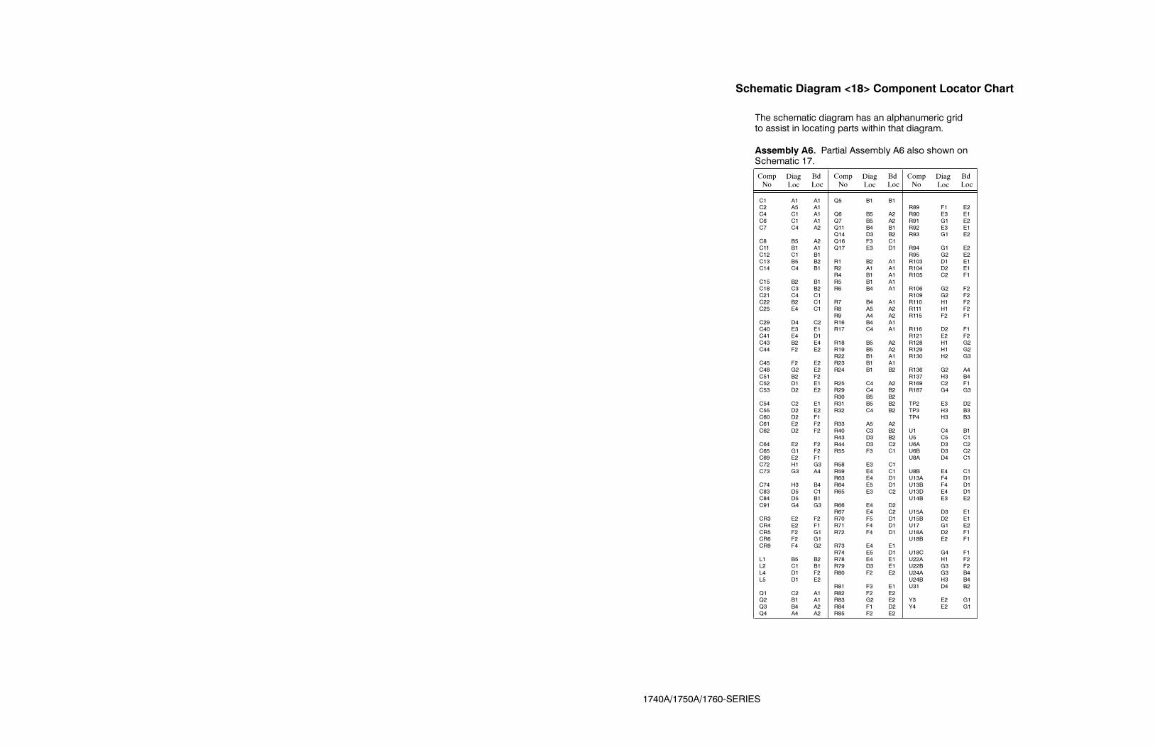
C1 A1 A1C2 A5 A1C4 C1 A1
C6 C1 A1
C7 C4 A2
C8 B5 A2C11 B1 A1
C12 C1 B1C13 B5 B2C14 C4 B1
C15 B2 B1
C18 C3 B2C21 C4 C1
C22 B2 C1
C25 E4 C1
C29 D4 C2C40 E3 E1
C41 E4 D1
C43 B2 E4
C44 F2 E2
C45 F2 E2
C48 G2 E2
C51 B2 F2
C52 D1 E1C53 D2 E2
C54 C2 E1
C55 D2 E2C60 D2 F1
C61 E2 F2
C62 D2 F2
C64 E2 F2C65 G1 F2
C69 E2 F1
C72 H1 G3
C73 G3 A4
C74 H3 B4
C83 D5 C1
C84 D5 B1
C91 G4 G3
CR3 E2 F2
CR4 E2 F1
CR5 F2 G1CR6 F2 G1
CR9 F4 G2
L1 B5 B2L2 C1 B1
L4 D1 F2
L5 D1 E2
Q1 C2 A1Q2 B1 A1
Q3 B4 A2
Q4 A4 A2
Q5 B1 B1
Q6 B5 A2
Q7 B5 A2Q11 B4 B1Q14 D3 B2
Q16 F3 C1
Q17 E3 D1
R1 B2 A1R2 A1 A1
R4 B1 A1
R5 B1 A1
R6 B4 A1
R7 B4 A1
R8 A5 A2
R9 A4 A2
R16 B4 A1R17 C4 A1
R18 B5 A2
R19 B5 A2R22 B1 A1
R23 B1 A1
R24 B1 B2
R25 C4 A2R29 C4 B2
R30 B5 B2
R31 B5 B2
R32 C4 B2
R33 A5 A2
R40 C3 B2
R43 D3 B2
R44 D3 C2R55 F3 C1
R58 E3 C1
R59 E4 C1R63 E4 D1
R64 E5 D1
R65 E3 C2
R66 E4 D2R67 E4 C2
R70 F5 D1
R71 F4 D1
R72 F4 D1
R73 E4 E1
R74 E5 D1
R78 E4 E1R79 D3 E1
R80 F2 E2
R81 F3 E1
R82 F2 E2R83 G2 E2
R84 F1 D2
R85 F2 E2
R89 F1 E2
R90 E3 E1
R91 G1 E2R92 E3 E1R93 G1 E2
R94 G1 E2
R95 G2 E2R103 D1 E1R104 D2 E1
R105 C2 F1
R106 G2 F2R109 G2 F2
R110 H1 F2
R111 H1 F2
R115 F2 F1
R116 D2 F1
R121 E2 F2
R128 H1 G2
R129 H1 G2R130 H2 G3
R136 G2 A4
R137 H3 B4
R169 C2 F1R187 G4 G3
TP2 E3 D2
TP3 H3 B3TP4 H3 B3
U1 C4 B1
U5 C5 C1
U6A D3 C2U6B D3 C2
U8A D4 C1
U8B E4 C1U13A F4 D1
U13B F4 D1
U13D E4 D1
U14B E3 E2
U15A D3 E1
U15B D2 E1
U17 G1 E2
U18A D2 F1U18B E2 F1
U18C G4 F1
U22A H1 F2U22B G3 F2
U24A G3 B4
U24B H3 B4
U31 D4 B2
Y3 E2 G1
Y4 E2 G1
Schematic Diagram <18> Component Locator Chart
The schematic diagram has an alphanumeric gridto assist in locating parts within that diagram.
Assembly A6. Partial Assembly A6 also shown onSchematic 17.
CompNo
DiagLoc
BdLoc
CompNo
DiagLoc
BdLoc
CompNo
DiagLoc
BdLoc
1740A/1750A/1760-SERIES

R1291.00K
+8V
Q5
R234.75K
+8V
+8V
<17>
<17>
B3
A3
REF_VIDEO
R242.21K
R413.0K
R22.21K
R54.75K
Q2
C151PF
---8V ---8V
R14.75K
C4430PF
C12200PF
R22100.0
C11430PF
L29UH
C6450PF
Q1
BURST
4
5
2
3
116
8
U18AMC10107
R10310.0 L5
9UHL49UH
C52.1UF
C62220PF
C55150PF
+5V
+5V
SYNC LOCKED OSCILLATOR
7
9
11
10
U18BMC10107
R89
475.0
R945.62K
R845.62K
R8210.0K
C45.01UF
8
10
1
4
6
12
5
2 314
U171496P
R91100.0
R93100.0
R1064.75K
C65240PF
C72.1UF
R1101.00K
R1308.25K
R1283.32K
R1111.00K
3
21
8
4
U22ALM393
+8V
REF SCH
C4810UF
R9510.0
R1094.75K
+5V---8V
R8010.0K
R835.62K
R855.62K
C44.01UF
CR5
R115402.0
CR6
---8V---8V
NC
+3.6V
VCOADJ
NTSC
VCOADJ
PAL
Y33.587412MHZ
Y44.4375MHZ
C691.2---4.0PF
R121100.0K
C61430PF
C641.2---4.0PF
+8V
CR3
CR4
+3.6V
NCNC
C53.1UF
R1162.49K
R1041.30K
C601000PF
R169232.0
R105232.0
+5V
+1.8VREF
C22.1UF
C43.1UF
/NTSC
+8V
+5V
C54.1UF
C51.1UF
C15.1UF
+8V
/NTSC
1.26V P---P
---8V
/NTSC
---8V/NTSC
2
31
8
4
U15ALM393
6
57
U15BLM393
R791.30K
+5V+8V
+1.8VREF
+1.8VREF
/PAL
R58232.0
R434.42K
R90121.0K
R92121.0K
TP2+8V
+8V
R55232.0
R81402.0
+8V
C73560PF
CX
14
RX
15
A1
B2 C
L
3
Q13
Q4
U24A74HC221
R136100.0K
+5V
+5V
+5V
<17>
F2
R137100.0K
TP3
NTSC_PULSES
+5V
<17>
NC
F2TP4
PAL_PULSES
C74560PF
CX
6
RX
7
A9
B10 C
L
11
Q5
Q12
U24B74HC221
6
57
U22BLM393
+5VC91
100PF
R71100.0
Q16
+1.8VREF
R657.32K
R6623.7K
R6751.1K
5
67
U14BTL072
Q14 C404700PF
Q17
R73301.0K
C411000PF
+8V
2
31
8
4
U6ATL072
R4412.1K5
67
U6BTL072
C18.1UF
+8V
---8V
+5VREG
<17>
B3R40
100.0K
3 5
16 2
8 7 4
U1LF398
C144700PF
REF_CAL
+8V
C3
50% POINT DETECTOR
<17>
R16100.0
R62.21K
Q6
Q3
R710.0K
Q4
R82.49K
C247UF
R9681.0
ST_SAMPLE
+8V
+8V
+8V
R291.00K
R321.00K
R1747.5K
R2547.5K
Q11
C7.1UF
C214700PF
+8V
---8V
COMP SYNC
70NS --- 400NS
+
---
50%SYNC
+IN2
--- IN3
OUT7
OUT8
LE5
GND6
---V4
+V1
U31MAX9686
+5V
CX
1
RX
2
A4
B5 C
L
3
Q6
Q7
U8A96LS02
126.2NS
126.2NS
+1V
0VNC
C2933PF
C2533PF
R595.76K
R63806.0
R78200.0
+5V
+5V
CX
15
RX
14
A12
B11 C
L
13
Q10
Q9
U8B96LS02
+1V
R72100.0
1
2
3
4
5
U13DCA3046
8
6
7
U13ACA3046
11
9
10
U13BCA3046
+8V
R18710.0K
CR9
NCNC
14
15
12
13
U18CMC10107
126.2NS0V
R703.01K
---8V
R64806.0
R74200.0
+5V
<17>
C4
C83.1UFC84
.1UF
SYNC_GATE
+5VREG
---5VREG
+5VREG
---5VREG
SYNC DELAY &
CHARGE PUMP COMPARATOR
R31475.0
R304.75K
3 5
16 2
8 7 4
U5LF398
L115UH
+8V
---8V
---8V
R193.01K
R3310.0K
C1343PF
C885PF
Q7
R1820.0K
/NTSC
+5V---8V
---8V
1750A/1760--SERIES (OPTION SC)
<17>
C3
BURST_GATEBURST_GATE
REFERENCE SCH <18>
PART OF A6 SCH BOARD

A7 Component Board
Static Sensitive DevicesSee Maintenance Section
C1 B1 C2C2 B2 D2
C3 B2 D2
C5 D1 I1
C8 C1 B3C9 C2 I2
C18 C3 C3
C19 C3 D3
C25 D4 D2
C28 C4 D3
C41 E1 G3
C42 E2 F3
C46 D2 F4C47 E2 F3
C48 E1 F4
C51 E3 E3
C52 E3 E3
C53 D3 D3C57 E2 D4
C61 E4 A4
C62 E4 C3C63 D4 B3
C66 E4 C4
C73 G4 G4
C74 G4 G4
C75 G5 G4C80 G1 B1
C90 G2 B2
C91 B5 B1
C92 C5 B2
C100 G3 B3
C180 D5 F1
C181 D5 F1C190 E5 F2
C191 F5 F2
C408 D1 C2
C418 D3 D2C428 D4 D3
C604 C5 C3
C605 B5 B3
C606 C5 D3C607 C5 A4
C608 C5 A1
CR1 C1 B2CR2 C2 B2
CR3 C2 C2
CR11 C3 C2
CR12 C3 C2
CR13 C4 C2
CR21 C4 D2
CR22 C5 D2
CR23 C5 D2CR180 D5 F2
CR181 D5 F1
CR190 E5 F2
CR191 E5 F2
J9 A1 D1
J81 H1 A1
J82 H2 A1
J83 H3 A2
Q1 C1 A1
Q2 C2 B2Q3 C2 B2
Q4 C1 B2
Q5 C1 B2
Q11 C3 C2Q12 C3 C2
Q13 C4 C2
Q14 C3 C2Q15 C3 C2
Q21 C4 D2
Q22 C4 D2
Q23 C5 D2
Q24 C5 D2Q25 C4 D2
Q51 F1 E4
Q52 G3 E4
Q53 F3 C4
Q54 G4 C4Q61 F4 B4
Q62 G5 A4
Q201 A5 E1Q204 A4 E2
Q207 A4 E2
Q210 F5 E1
R2 B2 B2R3 B2 C2
R4 B1 B2
R5 B2 B2
R6 B2 C2R7 C1 B2
R8 C1 B3
R9 C2 C3R11 B3 C2
R12 B3 C2
R13 B4 C2R14 B3 C2
R15 B3 C2
R16 B4 C2
R17 C3 C2
R18 C3 C3R19 C3 C3
R20 B1 A1
R21 B4 D2
R22 B4 C2
R23 B5 D2
R24 B4 D2
R25 B5 D2
R26 B5 D2R27 C4 D2
R28 C4 D3
R29 C5 D3
R40 D1 E3R41 D1 E3
R42 D1 F3
R43 D1 F3
R44 E1 F3R45 D2 F3
R46 D2 F4
R47 E2 F3
R48 E1 F4R49 F2 E3
R50 G3 E4
R51 D2 D3R52 D2 D4
R53 D3 D3
R54 D3 E3R55 D3 D3
R56 E3 D3
R57 E3 D4
R58 F3 C3
R59 G3 C3R60 D4 B4
R61 D4 B4
R62 D4 B3
R63 D4 C3
R64 D4 C3
R65 E4 C3
R66 E4 C4
R67 F4 A4R68 G5 A4
R70 G3 G3
R71 H3 G3
R72 G5 G2R73 G5 G2
R74 G4 G4
R75 G4 G4
R76 H4 H4R77 H4 H4
R78 H5 H4
R79 H5 H4
R80 G1 A2R81 G1 A2
R82 H1 B2
R83 G1 A2
R85 H1 A1
R90 G2 A2
R91 G2 A3R92 H2 B2
R93 G1 A3
R95 H2 A2R100 G3 A3
R101 G2 A3R102 H3 B3
R103 G2 A3
R105 H3 A3R201 A5 E1
R202 A5 E2
R203 A5 E1
R204 A4 E2
R205 A4 E2R206 A4 E2
R207 A4 E2
R208 A5 E2
R209 A4 E2
R210 F5 E1
R211 F5 E1
R301 F2 E4
R302 F3 D4R303 F4 B4
R408 C1 B3
R418 C3 C3
R428 C4 D3
U40A F2 F3
U40B F1 F3U40C D2 F3
U40D E1 F3
U41 E1 F4
U51A F3 D3U51B F3 D3
U51C E2 D3
U51D F2 D3U52A F5 B3
U52B F4 B3
U52C E4 B3
U52D F4 B3
U61 E4 C4U70 G4 G4
U80 G1 A1
U90 G2 A2
U100 G3 A3
U180 D5 F2U190 E5 F1
U212 E3 E4
U603A A5 L3
VR4 D1 C3
VR14 D3 C3
VR24 D4 D2
VR201 A5 E1
VR204 A4 E2VR207 A4 E2
Schematic Diagram <19> Component Locator ChartThe schematic diagram has an alphanumeric grid to assist in locating parts within that diagram.
Assembly A7. Partial Assembly A7 also shown on Schematic 20.
1740A/1750A/1760-SERIES
CompNo
DiagLoc
BdLoc
CompNo
DiagLoc
BdLoc
CompNo
DiagLoc
BdLoc
CompNo
DiagLoc
BdLoc
CompNo
DiagLoc
BdLoc
Board locator chart is on the back of Schematic 19.
CompNo
DiagLoc
BdLoc
CompNo
DiagLoc
BdLoc
R122
R158
R160
R159
R119
R123

R811.00K
R8339.2K
RGB OUTPUT
BETARGB TRANSCODERBETA<20>
C2
INPUT SELECTIONLTNG_Y <20>
H21A
1
1B2
2A3
2B4
3A5
3B6
4A7
4B8
5A9
5B10
6A11
6B12
7A13
7B14
8A15
8B16
9A17
9B18
10A19
10B20
11A21
11B22
12A23
12B24
13A25
13B26
14A27
14B28
15A29
15B30
16A31
16B32
17A33
17B34
18A35
18B36
19A37
19B38
20A39
20B40
J9
LTNG_X
GBR_INT
VIDEO_B3SEL_CMPST
<20>
<20>
H4
H5
CR1R42.43K
R75.11K
Q1
Q2
R84.75K
Q4
+8V
+8V
+8V+8V
+8V
C1.1UF
R91.00K
R20100.0
Q5
R4019.6K
R419.53K
R431.96K
R451.50K
VR4
Y
Pr
Pb+8V
+8V
R40810.0
C8150PF
C408.1UF
C5.1UF
R428.25K
R482.00K
C487.5PF
R442.00K
C41.1UF
R464.75K
R472.00K
+8V
3
2
1 8
6
7
4
U41LM6361
15 14
16
U40DDG444
Q51
G
+8V
7 6
8
U40BDG444
R301100.0
C80.1UF
R801.00K
3
1
412
11
13
5
6
147
9
U80EL2090
R822.00K
R9339.2K
+8V
---8V
R911.00K
G
OPT_PLS
REARPANEL
<20>
B5
J81R8575.0
B
J82R9575.0
REARPANEL
R922.00K
3
1
412
11
13
5
6
147
9
U90EL2090
+8V
---8V
C90.1UF
R901.00K
R10339.2K
R493.92K
GBR
/GBR
G
B
Y
+8V
---8V
+5V
---8V
2 3
1
12
13
45
U40ADG444
C42.1UF
C477.5PFC46
33PF
BETA
---8V
<20>
D2
1011
9U40CDG444
Y
BETA
C9.1UF
R52.43K CR2
R2100.0
C3.1UF
C2.1UF
Q3
+8V
+8V
+8V
---8V
R3100.0
CH 1 DRIVER
VIDEO_A3
VIDEO_A1
VIDEO_B1
VIDEO_A2
VIDEO_B2SEL_A
J9CONNECTSTO J13
<3>
A3MAINBOARD
SEL_B
VIDEO_A1
VIDEO_B1
SEL_CMPST
+11V
---11V
R11100.0
R142.43K CR11
CR3
R184.75K
Q11R175.11K
+8V +8V
+8V
R62.43K
CH 2 DRIVER
Q15
R532.50K
R512.00K
Y
+8V+8V
VR14C418.1UF
C18150PF
R41833.2
R552.00K
C52.1UF
C51.1UF
3
2
1 8
6
7
4
U212LM6361
R542.50K
C5710PF
R562.00K
R572.50K
C5312PF
R521.50K
+8V
10 11
9
U51CDG444
R583.92K
15 14
16
U51DDG444
GBR
B
R+8V
---8V
Q53
R302100.0
7 6
8
U51BDG444
3
1
412
11
13
5
6
147
9
U100EL2090
R1022.00K
R1001.00K
R1011.00K
+8V
---8V
C100.1UF
R
J83R10575.0
B---G
G+B <20>
D5
D1
R762.00K
R702.00K
R501.00K
R591.00K
+8V
+8V
---8V
---8V
Q54
Q52
R712.00K
DIAMOND TRANSCODER
15 14
16
U52DDG444
/GBR
G
B
Pb
+8V
+5V
---8V
2 3
1
12
13
45
U51ADG444
R611.91K
C6612PF
BETA
---8V
<20>
D3
10 11
9
U52CDG444
R601.00K
Pb
Pb
Pb
C19.1UF
CR12
R12100.0
R152.43K
R13100.0
CR13R162.43K
Q14Q12
Q13
+8V
+8V
---8V
R191.00K
9.1V
R2047.50K
R20610.0K
VIDEO_A2
VIDEO_B2
SEL_A
SEL_BSEL_A
+3V
Q204
VR204
SEL_A
<20>
D4
SEL_B
<20>
D4
9.1V
R20810.0K
R20910.0K
R2077.50K
R20510.0K
VIDEO_A3
SEL_CMPST
SEL_B
+3V
---8V
---8V
Q207
VR207
R21100.0
R22100.0
R242.43K CR21
Q21
Q22
Q24
R275.11K
R284.75K
+8V
+8V
+8V
+8V
CH 3 DRIVER
C25.1UF
Q25
R621.00K
Pr
Y
+8V+8V
R42875.0
C28150PF
C428.1UF
VR24
C62.1UF
3
2
1 8
6
7
4
U61LM6361
R652.00K
R642.00K
R632.00K
R662.00K
C61.1UF
C6327PF
+8V
---8V
7 6
8
U52BDG444
R673.92K
GBR
R
+8V
+8V
---8V
+5V
Q61
R303100.0
R742.00K
R782.00K
C73.1UF
C75.1UF
R752.00K
R772.00K
+8VC745---25PF
3
2
1 8
6
7
4
U70LM6361
DIAMONDTRANSITIONS
<20>
R---G <20>
D5
R792.00K
R722.00K
R732.00KR68
1.00K
+8V
---8V
---8V
Q62
G+R <20>
D4
R21012.1K
R21110.0K
/GBR
R
Pr
+8V
+8V
---8V
+3V
---8V
Q210
C19110UF
2 3
1
12
13
45
U52ADG444
GBR
/GBR
---11V+8V
<20> <20>
D2 C2
C18110UF
IN2
OUT3G
1
U1907908ACT
C190.1UF CR191
CR180
Pr
Pr
+11V
C604.1UF
IN1
OUT3
G
2
U1807808ACT
CR181C180.1UF
R252.43K
R23100.0
R262.43K
CR22
CR23
Q23
+8V
+8V +8V +8V
---8V
R291.00K
C605.1UF
C92.1UF
C606.1UF
C607.1UF
C608.1UF
C91.1UF
9.1VR20310.0K
R20210.0K
R2017.50K
VIDEO_B3
SEL_B
SEL_A
SEL_CMPST
+3V
---8V
---8V
---8V
Q201
VR201
2
31
U603A74HC02
1760--SERIES
---8V---8V ---8V---8V CR190
INPUTS, TRANSCODERS, & RGB OUTPUTS <19>
PART OF A7 COMPONENT BOARD
C36 A5 J2C111 E2 H2
C118 G1 I1C119 G2 I1
C120 G1 I1
C121 G2 I1
C130 F3 H1C131 F2 H1
C133 G2 H1C134 G3 H1
C135 G3 H1
C136 G3 G1C141 E4 H3
C151 F4 I4C152 G4 I4
C155 G4 I4C156 G5 I3
C162 G4 J3
C163 G3 J3
C164 G3 J4
C165 G4 J4
C170 G5 J3
C172 G5 J3
C174 G5 I2C176 H5 I2
C202 B3 N2
C205 C4 N3C206 C4 M3
C207 C4 K2
C338 G2 H1
C358 H4 J4C601 C5 L4
C603 D5 K4
J12 A3 L1
J13 A1 O1
Q111 E2 H3
Q112 F1 H2
Q114 F1 H2Q116 F2 H2
Q127 E3 H2Q131 F2 H1
Q134 G2 H1Q136 G2 G1Q143 E4 H2
Q151 G4 I3
Q157 G4 I4
Q180 E4 H4
R36 A5 J2
R110 E2 G3
R111 E2 H3
R112 F1 H2R113 F1 H3
R114 F1 I2
R115 F2 H2
R116 F2 H2R117 F1 I3
R118 F1 I2
R119 G1 I2R120 G1 I1
R121 G2 I1
R122 H1 I2
R123 G1 I2
R124 F2 H2
R125 F2 H2R126 F3 H2
R127 E3 H2
R128 E3 H2
R130 F2 H1
R131 F2 H1
R132 F3 H1
R133 F3 H1R134 G3 H1
R135 G2 H1R136 G2 H1
R137 G3 G2R140 E4 H2
R141 E3 H3
R142 E4 H3
R143 F4 H2R150 E5 H4
R151 F4 I4
R152 F4 I4
R153 G5 I3
R155 G4 I3
R156 G4 I4
R157 H4 I4
R158 H3 J4
R159 H3 J4
R160 G3 J4
R162 G4 J3R163 G3 J4
R164 F4 I4
R170 F5 I3
R171 F5 J2R172 F5 J3
R173 G5 J2R174 G5 I2
R175 G5 I2
R176 H5 I3R177 H5 I3
R180 E4 H4
R181 E4 H4
R312 E2 H3R336 G2 G1
R338 H2 G1
R358 H4 J4R601 C4 L3
R602 C5 L3
R603 D5 K4
U101A E2 G3U101B E1 G3
U101C E1 G3
U101D E2 G3
U102A H2 G1
U102B H3 G1
U102C E4 G1
U102D H2 G1
U103A E3 G2U103B E3 G2
U103C E4 G2
U103D E3 G2U124A G1 H2
U124B G1 H2
U124C G1 H2
U124D G1 H2U125A G1 J1
U125B G2 J1U125C G3 J1U125D G4 J1
U126A G1 I2U126B G1 I2
U151A E4 H3U151B E5 H3
U151C E5 H3
U151D E5 H3
U161A H4 J3
U161B F3 J3
U161C F4 J3U161D H3 J3
U162A G3 J4
U162B G4 J4
U171 G5 I3U202 B2 N2
U203 C1 N3
U204 B4 M2U205 C2 N3
U206 B3 M3
U207 C4 K2
U208 C3 L2
U209 C3 L3
U211A C1 M2
U211B C2 M2
U602A C5 L4U602B D5 L4
U603B E5 L3
U603C E5 L3
U603D E5 L3
Schematic Diagram <20> Component Locator Chart
The schematic diagram has an alphanumeric grid to assist in locating parts within thatdiagram.
Assembly A7. Partial Assembly A7 also shown on Schematic 19.
1740A/1750A/1760-SERIES
CompNo
DiagLoc
BdLoc
CompNo
DiagLoc
BdLoc
CompNo
DiagLoc
BdLoc
CompNo
DiagLoc
BdLoc
C1 19 B1 C2C2 19 B2 D2C3 19 B2 D2
C5 19 D1 I1
C8 19 C1 B3C9 19 C2 I2
C18 19 C3 C3
C19 19 C3 D3
C25 19 D4 D2
C28 19 C4 D3
C36 20 A5 J2
C41 19 E1 G3C42 19 E2 F3C46 19 D2 F4
C47 19 E2 F3
C48 19 E1 F4
C51 19 E3 E3C52 19 E3 E3C53 19 D3 D3
C57 19 E2 D4
C61 19 E4 A4C62 19 E4 C3
C63 19 D4 B3
C66 19 E4 C4
C73 19 G4 G4
C74 19 G4 G4C75 19 G5 G4
C80 19 G1 B1
C90 19 G2 B2
C91 19 B5 B1
C92 19 C5 B2
C100 19 G3 B3
C111 20 E2 H2
C118 20 G1 I1C119 20 G2 I1
C120 20 G1 I1
C121 20 G2 I1
C130 20 F3 H1C131 20 F2 H1
C133 20 G2 H1
C134 20 G3 H1C135 20 G3 H1
C136 20 G3 G1
C141 20 E4 H3
C151 20 F4 I4
C152 20 G4 I4C155 20 G4 I4
C156 20 G5 I3
C162 20 G4 J3
C163 20 G3 J3
C164 20 G3 J4
C165 20 G4 J4
C170 20 G5 J3
C172 20 G5 J3C174 20 G5 I2
C176 20 H5 I2
C180 19 D5 F1
C181 19 D5 F1C190 19 E5 F2
C191 19 F5 F2
C202 20 B3 N2
C205 20 C4 N3C206 20 C4 M3
C207 20 C4 K2
C338 20 G2 H1
C358 20 H4 J4C408 19 D1 C2
C418 19 D3 D2
C428 19 D4 D3
C601 20 C5 L4
C603 20 D5 K4
C604 19 C5 C3
C605 19 B5 B3
C606 19 C5 D3C607 19 C5 A4
C608 19 C5 A1
CR1 19 C1 B2
CR2 19 C2 B2
CR3 19 C2 C2CR11 19 C3 C2
CR12 19 C3 C2CR13 19 C4 C2
CR21 19 C4 D2CR22 19 C5 D2
CR23 19 C5 D2
CR180 19 D5 F2
CR181 19 D5 F1CR190 19 E5 F2CR191 19 E5 F2
J9 19 A1 D1J12 20 A3 L1J13 20 A1 O1
J81 19 H1 A1
J82 19 H2 A1
J83 19 H3 A2
Q1 19 C1 A1
Q2 19 C2 B2
Q3 19 C2 B2
Q4 19 C1 B2Q5 19 C1 B2
Q11 19 C3 C2
Q12 19 C3 C2
Q13 19 C4 C2Q14 19 C3 C2
Q15 19 C3 C2
Q21 19 C4 D2
Q22 19 C4 D2Q23 19 C5 D2
Q24 19 C5 D2
Q25 19 C4 D2
Q51 19 F1 E4Q52 19 G3 E4
Q53 19 F3 C4
Q54 19 G4 C4
Q61 19 F4 B4
Q62 19 G5 A4
Q111 20 E2 H3
Q112 20 F1 H2
Q114 20 F1 H2Q116 20 F2 H2
Q127 20 E3 H2
Q131 20 F2 H1
Q134 20 G2 H1Q136 20 G2 G1Q143 20 E4 H2
Q151 20 G4 I3
Q157 20 G4 I4Q180 20 E4 H4
Q201 19 A5 E1
Q204 19 A4 E2
Q207 19 A4 E2Q210 19 F5 E1
R2 19 B2 B2
R3 19 B2 C2
R4 19 B1 B2R5 19 B2 B2
R6 19 B2 C2
R7 19 C1 B2
R8 19 C1 B3R9 19 C2 C3
R11 19 B3 C2
R12 19 B3 C2
R13 19 B4 C2R14 19 B3 C2
R15 19 B3 C2
R16 19 B4 C2
R17 19 C3 C2R18 19 C3 C3
R19 19 C3 C3R20 19 B1 A1R21 19 B4 D2
R22 19 B4 C2
R23 19 B5 D2
R24 19 B4 D2R25 19 B5 D2
R26 19 B5 D2
R27 19 C4 D2R28 19 C4 D3
R29 19 C5 D3
R36 20 A5 J2
R40 19 D1 E3R41 19 D1 E3
R42 19 D1 F3
R43 19 D1 F3R44 19 E1 F3R45 19 D2 F3
R46 19 D2 F4
R47 19 E2 F3
R48 19 E1 F4R49 19 F2 E3
R50 19 G3 E4
R51 19 D2 D3
R52 19 D2 D4R53 19 D3 D3
R54 19 D3 E3
R55 19 D3 D3
R56 19 E3 D3R57 19 E3 D4
R58 19 F3 C3
R59 19 G3 C3
R60 19 D4 B4
R61 19 D4 B4
R62 19 D4 B3
R63 19 D4 C3
R64 19 D4 C3R65 19 E4 C3
R66 19 E4 C4
R67 19 F4 A4
R68 19 G5 A4R70 19 G3 G3
R71 19 H3 G3
R72 19 G5 G2
R73 19 G5 G2R74 19 G4 G4
R75 19 G4 G4
R76 19 H4 H4
R77 19 H4 H4R78 19 H5 H4
R79 19 H5 H4
R80 19 G1 A2
R81 19 G1 A2
R82 19 H1 B2
R83 19 G1 A2
R85 19 H1 A1
R90 19 G2 A2R91 19 G2 A3
R92 19 H2 B2
R93 19 G1 A3
R95 19 H2 A2
R100 19 G3 A3R101 19 G2 A3
R102 19 H3 B3
R103 19 G2 A3R105 19 H3 A3
R110 20 E2 G3
R111 20 E2 H3
R112 20 F1 H2
R113 20 F1 H3R114 20 F1 I2
R115 20 F2 H2
R116 20 F2 H2
R117 20 F1 I3
R118 20 F1 I2R119 20 G1 I2R120 20 G1 I1
R121 20 G2 I1
R122 20 H1 I2R123 20 G1 I2
R124 20 F2 H2R125 20 F2 H2
R126 20 F3 H2
R127 20 E3 H2
R128 20 E3 H2
R130 20 F2 H1
R131 20 F2 H1R132 20 F3 H1R133 20 F3 H1
R134 20 G3 H1
R135 20 G2 H1R136 20 G2 H1R137 20 G3 G2
R140 20 E4 H2
R141 20 E3 H3R142 20 E4 H3
R143 20 F4 H2
R150 20 E5 H4
R151 20 F4 I4
R152 20 F4 I4R153 20 G5 I3
R155 20 G4 I3
R156 20 G4 I4
R157 20 H4 I4
R158 20 H3 J4
R159 20 H3 J4
R160 20 G3 J4
R162 20 G4 J3R163 20 G3 J4
R164 20 F4 I4
R170 20 F5 I3
R171 20 F5 J2R172 20 F5 J3
R173 20 G5 J2
R174 20 G5 I2R175 20 G5 I2
R176 20 H5 I3
R177 20 H5 I3
R180 20 E4 H4
R181 20 E4 H4R201 19 A5 E1
R202 19 A5 E2
R203 19 A5 E1
R204 19 A4 E2
R205 19 A4 E2
R206 19 A4 E2
R207 19 A4 E2
R208 19 A5 E2R209 19 A4 E2
R210 19 F5 E1
R211 19 F5 E1
R301 19 F2 E4R302 19 F3 D4
R303 19 F4 B4
R312 20 E2 H3
R336 20 G2 G1R338 20 H2 G1
R358 20 H4 J4
R408 19 C1 B3
R418 19 C3 C3R428 19 C4 D3
R601 20 C4 L3
R602 20 C5 L3
R603 20 D5 K4
U40A 19 F2 F3
U40B 19 F1 F3
U40C 19 D2 F3
U40D 19 E1 F3U41 19 E1 F4
U51A 19 F3 D3U51B 19 F3 D3U51C 19 E2 D3
U51D 19 F2 D3
U52A 19 F5 B3
U52B 19 F4 B3U52C 19 E4 B3
U52D 19 F4 B3
U61 19 E4 C4U70 19 G4 G4
U80 19 G1 A1
U90 19 G2 A2
U100 19 G3 A3U101A 20 E2 G3U101B 20 E1 G3
U101C 20 E1 G3U101D 20 E2 G3U102A 20 H2 G1
U102B 20 H3 G1
U102C 20 E4 G1
U102D 20 H2 G1U103A 20 E3 G2
U103B 20 E3 G2
U103C 20 E4 G2
U103D 20 E3 G2
U124A 20 G1 H2
U124B 20 G1 H2
U124C 20 G1 H2
U124D 20 G1 H2U125A 20 G1 J1
U125B 20 G2 J1
U125C 20 G3 J1
U125D 20 G4 J1
U126A 20 G1 I2U126B 20 G1 I2
U151A 20 E4 H3
U151B 20 E5 H3U151C 20 E5 H3
U151D 20 E5 H3
U161A 20 H4 J3
U161B 20 F3 J3U161C 20 F4 J3
U161D 20 H3 J3
U162A 20 G3 J4
U162B 20 G4 J4
U171 20 G5 I3
U180 19 D5 F2
U190 19 E5 F1
U202 20 B2 N2U203 20 C1 N3U204 20 B4 M2
U205 20 C2 N3
U206 20 B3 M3
U207 20 C4 K2U208 20 C3 L2
U209 20 C3 L3
U211A 20 C1 M2U211B 20 C2 M2
U212 19 E3 E4
U602A 20 C5 L4
U602B 20 D5 L4
U603A 19 A5 L3U603B 20 E5 L3
U603C 20 E5 L3
U603D 20 E5 L3
VR4 19 D1 C3
VR14 19 D3 C3
VR24 19 D4 D2
VR201 19 A5 E1
VR204 19 A4 E2VR207 19 A4 E2
A7 Component Board Component Locator Chart
CompNo
DiagNo
DiagLoc
BdLoc
(with cross-references to Schematics 19 and 20)
CompNo
DiagNo
DiagLoc
BdLoc
CompNo
DiagNo
DiagLoc
BdLoc
CompNo
DiagNo
DiagLoc
BdLoc
CompNo
DiagNo
DiagLoc
BdLoc
CompNo
DiagLoc
BdLoc

+8V
1
23
U125A74HC32
/TOP
OPT_PLS
C118.01UF
/TOP
OPT_PLS
VERTICALAMPLIFIER
OUTPUT SWITCHING2 3
1
U211A74HC125
MISO
SER10
A11
B12
C13
D14
E3
F4
G5
H6
CLK2
CLKINH15
SH/LD1
QH9
QH7
U20374HC165
1A1
1B2
2A3
2B4
3A5
3B6
4A7
4B8
5A9
5B10
6A11
6B12
7A13
7B14
8A15
8B16
9A17
9B18
10A19
10B20
11A21
11B22
12A23
12B24
13A25
13B26
14A27
14B28
15A29
15B30
16A31
16B32
17A33
17B34
18A35
18B36
19A37
19B38
20A39
20B40
J13
BA15
CONTROLLER
/ID_LD
BSCK
/OPT_EN
/OPT_EN
<19>
SW1
SW2
+5V
+8V
G+B
H3
10 11
9
U101CDG444
7 6
8
U101BDG444
R1142.74K
R1121.00K
+8V
+8V
+8V+8V
7 6
8
U124BDG444
1011
9
U124CDG444
R1131.00K
Q112
R1183.32K
R1172.21K
Q114
2 3
1
12
13
45
U124ADG444
+5V+8V
+8V
R12110.0K
R12010.0K
C121.1UF
C120.1UF
R12220K
15 14
16
U124DDG444
R119100.0K
R123392.0
5
67
U126BLF412ACN
3
21
8
4
U126ALF412ACN
---8V
+8V
---8V
R11910.0K
R12310.0K
LTNGREGIST
VERT
LTNG
---8V
+8V
+5V
23
1
12
13
4 5
U102ADG444
A1
/BOTTOM
OPT_PLS
+8V
+8V
---8V
---8V
C119.01UF
4
56
U125B74HC32
C338100PF
R1353.01KC133
105PF
R338100.0
R1155.11K
R1251.30K R130
1.00K
Q131
R116100.0
R1242.00K
Q116
/BOTTOM
+8V
---8V
---8V
OPT_PLS
R1311.00K
R111100.0
R11047.5K
R312100.0
Y
Pr
SW3
SW4
---8V
D5
D2
Q111C1112.5---9PF
2 3
1
12
13
45
U101ADG444
15 14
16
U101DDG444
5 6
4
U211B74HC125
BETA
GBR
/GBR
MISO
LTNG
/LTNG
/OPT_CS
<19>
<19>
<19>
<19>
<19>
D1
E5
E5
SER14
QA15
QB1
SCLK11
QC2
SCLR10
QD3
QE4
RCLK12
QF5
G13
QG6
QH7
QH’9
U20574HC595
A1
B2
C3
G16
G2A4
G2B5
Y015
Y114
Y213
Y312
Y411
Y510
Y69
Y77
U20274HC138
/OPT_CS
BMOSI
BSCK
+5V
/P_OPT_CS
BA15
BA4
BA3
CONNECTS
A3MAINBOARD
J13
TO J2
<10>
1A1
1B2
2A3
2B4
3A5
3B6
4A7
4B8
5A9
5B10
6A11
6B12
7A13
7B14
8A15
8B16
9A17
9B18
10A19
10B20
11A21
11B22
12A23
12B24
13A25
13B26
14A27
14B28
15A29
15B30
16A31
16B32
17A33
17B34
18A35
18B36
19A37
19B38
20A39
20B40
J12
MISO
BSCK
BMOSI
/OPT_CS
/OPT_EN
BA2
BA4
BA2
BA3
/P_OPT_CS
+5V
Q09
Q110
Q211
Q312
Q416
Q517
Q618
Q719
Q813
XO/HF20
D82
D724
D625
D526
D427
D33
D24
D15
D06
W1
R15
RS22
FL/RT23
XI7
FF8
EF21
DGND14
VCC28
U2067201
WR_FIFO
+5V
OPT_LTCH
D12
Q119
D23
Q218
D34
Q317
D45
Q416
D56
Q515
D67
Q614
D78
Q713
D89
Q812
CLK11
OC1
U20874HCT574
FD8
FD9
FD10
FD11
FD12
FD13
FD14
FD15
SW1
SW2
SW4
SW5
SW6
SW7
SW8
SW3
<19>
R127100.0
Pb
SW5
+8V
+8V
+5V
D3
Q127
1514
16
U103DDG444
BOWTIENULL
23
1
12
13
4 5
U103ADG444
C13077PF
/TOP
---8V
OPT_PLS
R1341.00K
C1355---25PF
R1331.00K
R1323.01K
C13170PF
TIMINGVECTOR
TIMING---8V
---8V
R336100.0
C13427PF
Q134
R136511.0
9
108
U125C74HC32
C1365---25PF
Q136
VECTORR1371.50K
76
8
U102BDG444
LTNG_Y
/LTNG
1514
16
U102DDG444
<19>
---8V
+8V
R15920K
+8V
R15810.0K
---8V
R16010.0K
HORIZLTNGREGIST
15 14
16
U161DDG444
2 3
1
12
13
45
U161ADG444
+5V
+8V
---8V
+8V
C164.01UF R163
10.0K
C163.1UF
R16210.0K
R158100.0K
C165.01UF
R160392.0
2
31
8
4
U162ALF412ACN
5
67
U162BLF412ACN
R126649.0
7 6
8
U161BDG444
1011
9
U161CDG444
R143619.0
HORIZONTAL
AMPLIFIER
R128649.0
R14110.0K
R14210.0K
SW6
SW7
SW8
---8V
---8V
G+R
---8V
C141.47UF
Q143
G5
1011
9
U102CDG444
10 11
9
U103CDG444
7 6
8
U103BDG444
D12
Q119
D23
Q218
D34
Q317
D45
Q416
D56
Q515
D67
Q614
D78
Q713
D89
Q812
CLK11
OC1
U20974HCT574
FD8
FD9
FD10
FD11
FD12
FD13
FD14
FD15
SW9
SW10
SW11
/TOP
/BOTTOM
LTG_BK_EN
<19>
<19>
A3
BD8
BD9
BD10
BD11
BD12
BD13
BD14
BD15
FD8
FD9
FD10
FD11
FD12
FD13
FD14
FD15
WR_FIFO
IRQ5
C202.1UF
D12
Q119
D23
Q218
D34
Q317
D45
Q416
D56
Q515
D67
Q614
D78
Q713
D89
Q812
CLK11
OC1
U20474HCT574
BD9
BD8
BD11
BD10
+5V
CONNECTS
A3MAINBOARD
J12
TO J5
<10>
BD15
BD14
BD13
BD12BD8
BD9
BD10
BD11
BD12
BD13
BD14
BD15
OPT_LTCH
/OPT_BLANK
LR_GO
C206.1UF
B16MHZ
BLANK_CK
IRQ5
+5V
I/CK2
I3
I4
I5
I6
I7
I9
I10
I11
I12
I13
I16
I/O27
I/O26
I/O25
I/O24
I/O23
I/O21
I/O20
I/O19
I/O18
I/O17
U20722V10---25
C205.1UF
C207.1UF
SEL_A
SEL_B+5V+5V
+5V
+5VR60120K
<19>
A4
SYNC
BLANKING
SYNC
BLANKING
R14047.5K
Q180
SW9
SW10
+8V+5V
---8V
2 3
1
12
13
45
U151ADG444
15 14
16
U151DDG444
R180100.0
R1521.00K
R1813.01K
R170100.0
/BOTTOM
+8V
---8V
---8V
OPT_PLS
R1511.00K
C15177PF
R1643.92K
12
1311
U125D74HC32
C155105PF
C15636PF
C162.1UF
R1551.00K
R1533.01K
R1561.00K
Q151
R1571.50K
+8V
---8V
---8V
Q157
/BOTTOM
OPT_PLS
C15270PF
R358100.0
LTNG_X
+8V
C358100PF
<19>
A1
GBR_INT
+8V
<19>
A1
GBR
R173649.0
R17715.0K
R174100.0
C174330PF
R176100.0
C176100PF
+8V
---8V
+8V
8
10
1
4
6
12
5
2 314
U1711496P
INTENSIFICATION
C172.1UF
C170330PF
R1715.11K
+8V5
64
U603B74HC02
8
910
U603C74HC02
11
1213
U603D74HC02
R175100.0
R1725.11K
R15047.5K
SW11
SW1
SW8
R---G
B---G
H4
H5
10 11
9
U151CDG444
7 6
8
U151BDG444
R60268.1K
R6038.25K
LTG_BK_EN
+5V
<19>
<19>
C6031000PF
CX
15
RX
14
A12
B11 C
L
13
Q10
Q9
U602B96LS02
BLANK_CK
CX
1
RX
2
A4
B5 C
L
3
Q6
Q7
U602A96LS02
C6011800PF
OPT_PLS
B16MHZ
BLANK_CK
IRQ5
<19>
H1
R36100.0
1760--SERIES
OPT_PLSC36100PF
/OPT_BLANKOPT_PLS
CONTROL & SWITCHING <20>
---8V
PART OF A7 COMPONENT BOARD

A1 Power Supply Board Static Sensitive DevicesSee Maintenance Section
1740A/1750A/1760-SERIES
C1 22 F4 A2C2 22 B4 A4
C3 22 D3 A2
C4 22 B5 A4
C5 22 C5 A5C6 22 D3 B2
C7 22 D3 B2
C8 22 E2 B2
C9 22 D4 B3
C10 22 C4 B4
C11 22 C4 B4
C12 22 E2 B2
C13 22 D2 C4C14 22 F2 C5
C15 22 C2 C4
C16 22 D2 C4
C17 22 F3 C4
C18 22 D2 D4C19 22 F2 D5
C20 22 C2 D4
C21 21 H3 E1C22 22 B2 D2
C23 22 B3 E2
C24 22 B2 E3
C25 22 D1 E4
C26 22 A2 E1C27 22 B1 E3
C28 22 B1 E3
C29 21 F2 F3
C30 22 D1 F4
C31 21 F1 F1
C32 21 G2 F4C32 21 G2 F4
C33 21 F2 F3
C34 21 G1 G4
C35 21 G2 G4C36 21 F2 G3
C37 21 G2 G4
C38 21 G4 G5
C40 21 H1 H4
C41 21 F2 H1
C42 21 F4 H4
C43 21 G3 H5
C44 21 E5 I3C45 21 E5 H3
C46 21 D5 I4
C47 21 E5 I4
C48 21 C5 I4
C49 21 D5 I4C51 21 E2 I2
C52 21 E1 I3
C53 21 C3 I4C54 21 E5 I4
C55 21 D4 J4
C56 21 C5 J4
C57 21 D3 J3
C58 21 B5 J5C59 21 D2 J1
C60 21 C3 J4
C61 21 B5 J5
C62 21 D2 J3
C63 21 D3 J4
C64 21 C3 J4C65 21 A4 K4
C66 21 A1 K1
C67 21 A3 L4
C68 21 A3 L4C69 21 A4 L4
C70 21 A4 L5
C71 21 C1 L2
C72 21 A3 L4C74 21 B1 M1
C75 21 B1 M2
C76 21 C5 I5
C77 22 C5 A4
CR1 22 C4 A4
CR2 22 D4 B4
CR3 22 C4 B5
CR4 22 D5 B5CR5 22 E2 B1
CR6 22 E2 C1
CR7 22 D3 B2
CR8 22 D2 C4CR9 22 E2 C4
CR10 22 D2 D4
CR11 22 D2 D4
CR12 22 A2 E1CR13 22 A2 E1
CR14 22 B2 E2
CR15 22 C1 E4
CR16 21 F1 F2CR17 21 F2 G3
CR18 21 F2 G1
CR19 21 F2 G3CR20 21 D5 H4
CR21 21 C5 I5
CR22 21 E2 I1CR23 21 E2 I2
CR24 21 D3 J4
CR25 21 D2 J1
CR26 21 D3 J4
CR27 21 B5 J5CR28 21 E3 J3
CR29 21 B5 K5
CR30 21 A2 K4
CR31 21 B4 K4
CR32 21 B1 M4
CR33 21 C1 M3
CR34 21 B1 M3
CR35 21 C1 M3
DS1 22 E2 A1
DS2 22 E3 A1
DS3 22 E4 A3DS4 22 D3 B1
DS5 22 E4 B3
DS6 21 G3 F2
DS7 21 C1 M3
F1 21 B1 M1
FIL1 22 C3 C1
FIL2 22 C3 C1
J1 22 F3 B1
J2 22 F2 D1J3 21 F5 F4
J4 21 H4 F5
J5 21 H1 H4
J6 21 D2 J1J7 21 D1 K2
J8 21 A1 N2
L1 22 B2 D4
L2 22 D1 E4L3 21 G2 F3
L4 21 G1 G2
L5 21 G2 G1
L6 21 G2 G3L7 21 E2 I1
L8 21 D1 J1
P8 21 D2
P9 21 D1
Q1 22 E5 A3
Q2 22 E5 A3
Q3 22 C4 A4Q4 22 D4 B4
Q5 22 D4 B4
Q6 22 D4 B4
Q7 22 B2 D1
Q8 22 A2 E1
Q9 22 A2 E2
Q10 22 B2 E2
Q11 21 F3 E2Q12 21 D5 I4
Q13 21 E5 I4
Q14 21 E3 J3Q15 21 B2 K4
R1 22 E4 A2
R2 22 E4 A2R3 22 E4 A3
R4 22 E4 A3
R5 22 D5 A4
R6 22 B4 A4
R8 22 A4 A4R9 22 F4 A2
R10 22 B4 A4
R11 22 B4 A4
R12 22 D5 A4
R13 22 E3 A2
R14 22 E5 A3
R15 22 E5 A3
R16 22 D4 A4R17 22 C5 A4
R18 22 C4 A4
R19 22 D3 B1
R20 22 D3 B3R21 22 E5 A3
R22 22 B5 A4
R23 22 C4 B4
R24 22 C4 A4R25 22 C5 A5
R26 22 D3 B3
R27 22 D4 B3
R28 22 C4 B4R29 22 D4 B4
R30 22 E2 B1
R31 22 E3 B1
R32 22 E2 B3
R33 22 E3 C1
R34 22 D2 B3R35 22 F3 C4
R36 22 F1 C4
R37 22 F2 C4
R38 22 F2 C5
R39 22 E3 C1R40 22 C2 C3
R41 22 D2 C4
R42 22 E3 D1R43 22 F3 C4
R44 22 F2 C5
R45 22 F2 D1
R46 22 D2 D5
R47 22 F2 D1R48 22 F3 D1
R49 22 B3 D2
R50 22 D2 D5
R51 22 F3 D1
R52 21 G3 E1
R53 22 D2 E5
R54 22 B2 E2
R55 22 A2 E1R56 22 A2 E1
R57 22 B2 E1
R58 22 A2 E2
R59 22 B3 E2R60 22 B1 E2
R61 22 C2 E3
R62 21 F3 F2
R63 21 F3 F2
R64 21 G3 F2
R65 22 B2 E2R66 22 C2 E2
R67 22 C1 E3
R68 22 B1 E3
R69 21 G2 E5
R70 21 H1 F1R71 21 F4 G5
R72 21 G4 G5
R73 21 G4 G5R74 21 H4 G5
R75 21 F4 H5
R76 21 F4 G5
R77 21 F4 G4
R78 21 G4 H5R79 21 F4 H4
R80 21 G4 H5
R81 21 D5 H4
R82 21 D5 I4
R83 21 D5 H4
R84 21 E5 I3
R85 21 C5 I4
R86 21 B4 I4R87 21 B3 I4
R88 21 D2 J1
R89 21 C5 J4
R90 21 E4 J3R91 21 D4 J4
R92 21 D4 J4R93 21 D3 J4
R94 21 C3 J4
R95 21 B4 J5
R96 21 D3 J3R97 21 D3 J3
R98 21 C3 J4
R99 21 B2 J4
R100 21 B4 J4
R101 21 B3 K4
R102 21 A4 K4
R103 21 B5 K5
R104 21 B5 K5R105 21 B3 K4
R106 21 A3 K4
R107 21 A3 K4
R108 21 A2 K4
R109 21 B3 L4R110 21 A4 L4
R111 21 A3 L4
R112 21 B2 L3R113 21 A2 L4
R114 21 A4 L4
R115 21 A3 L4
R116 21 D1 L1
R117 21 C1 L3R118 21 C1 M3
R119 21 B2 M4
R120 21 C2 N4
R121 21 C2 M5
R122 21 D2 N5
R123 21 B1 N4R124 21 D5 I4
R125 21 C5 I4
R126 22 C5 A4
T1 22 C2 D3
T2 21 E5 H3
T3 21 E2 H3
TP1 21 F5 F4TP2 21 E3 I3
TP3 21 B5 K4
U1 22 D1 C2U2 22 B2 F4
U3A 21 G4 H5
U3B 21 F4 H5
U4 21 E4 H5
U5A 21 C5 I5U5B 21 C4 I5
U6 21 C3 J4
U7A 21 B4 K5
U7B 21 B3 K5U7C 21 B3 K5
U7D 21 B4 K5
U8A 21 B5 K5
U8B 21 A5 K5
VR1 21 F3 F2
VR3 21 C2 L5
W1 21 G2 E4W2 21 G2 E4
W3 21 G2 E4
A1 Power Supply Board Component Locator Chart
CompNo
DiagNo
DiagLoc
BdLoc
(with cross-references to Schematics 21 and 22)
CompNo
DiagNo
DiagLoc
BdLoc
CompNo
DiagNo
DiagLoc
BdLoc
CompNo
DiagNo
DiagLoc
BdLoc
CompNo
DiagNo
DiagLoc
BdLoc
CompNo
DiagNo
DiagLoc
BdLoc
CompNo
DiagNo
DiagLoc
BdLoc
CompNo
DiagNo
DiagLoc
BdLoc
CompNo
DiagNo
DiagLoc
BdLoc
CompNo
DiagNo
DiagLoc
BdLoc

+11V
R7010
CR16CR17CR18
ALL CIRCUITRY TO THELEFT OF THE ISOLATIONBOUNDARY IS AT POWER LINEPOTENTIAL AND REQUIRESAN ISOLATION TRANSFORMERTO SERVICE.
CAUTION:MOUNTING
C74.022UF
REARPANEL
J8
5 OHM COLD
90---250V
C75.068UF
F12A
C66.022UF
R118121K
R117121K
R123 CR32 CR33
CR34 CR35 DS7
R1168
L81MH
C71330UF
SNUBBER
INSTALLEDNORMALLY
BOUNDARYISOLATION
C52.47UF
1 2J7
P9
OUTPUT FILTERS
C A
H L447UH
C31560UF
CR16
W30 OHM
+11V
+11A
C34100UF
B1
C40100UF
12
J5
W20 OHM
R694.7
C3210UF
---11A
---11V
+40VA
+40V
+5V
C37100UF
C35330UF
H
H L34.7UH
L647UH
C41560UF L5
47UH
C3310UF
C291000UF
C361000UF
CR18
CR19
CR17L7
4.7UH
C51.47UF
C59330PF
3
10
8
14
13
12
11
9
2
1
4
5
6
7
T3
CR22
CR25 CR23
INSTALLEDNORMALLY
+16V
2W 5%
R120
100K
R122100K
R882.4K
+16VPRI
C62330UF
1 2
J6
P8
5.6V
R119150K
R121150K
+5VC
VR3
SHUTDOWN LOGIC
R992.00K
+5VPRI
R113499K
R112499K
+5VPRI
CR30
R11144.2K
C72100PF
R109301K
6
71
U7BLM339
R1082.00K
R1012.00K
+5VPRI
+16VPRI
+5VPRI
R115147K
CONTROLLER
R9440.2K
C53470PF
COMP1
VFB2
ISEN3
RT/CT4
REF8
VCC7
OUT6
GND5
U6UC3842
+5VPRI
Q15
SWITCHER
BASE DRIVE
C63.1UF
C64.1UF
+5VPRI +16VPRI
+16VPRI
CR24
CR26
H
Q14
TP2
5.1V
OVERVOLTAGE
PROTECTION
G
AQ11
R6310.0
R6410.0
+5V +5V
VR1
Q11
W10 OHM
R521.00K
+5V
+5D
+5VA
C2110UF
.2V
VOLTAGE
REFERENCE
PROTECTION,TOUCHTO TEST OVERVOLTNOTE:
R74 AND R78 TOGETHERWITH SCREWDRIVER TIP.
R8024.9K
C43.1UF
+5V
KK A G
NC
ERROR AMPLIFIER
R62100
C42.01UF
R7745.3K
DS6
BOUNDARYISOLATION
R911.00K
R9622.1
R90.51
CR28
R921.33K
C57.033UF
C55150PF
R972.21K
R93178
IF V > 1V = SHUTDOWN
C60.0047UF
R984.53K
+5VPRI
2.5V+3V
C67100PF
R8710.0K
R1073.01K
C68100PF
8
914
U7CLM339
C65.1UF
R1021.00K
+5VPRI
R105301K
R100100K
CR31
R10633.2K
R11022.1K
C70.1UF
4
52
3
12
U7ALM339
R864.32K
C69.1UF
11
1013
U7DLM339
R11433.2K
+5VPRI
+5VPRI
ERROR VOLTAGE
NC
NC
R954.99K
+5VCTRANSFORMER DRIVER
NC
NCCL
11
CX6
RX7
B10
A9
Q12
Q5
U5B74HC221 NC
1
2
5
4
6
U4MOC1005
+5VPRI
R762.00K
R7210.0K
R712.00K
C38.1UF
R7515.0K
2
5
63
U3BLM10R79
1.00K
+5V
+5V ADJ
NC2.5V
<22>
D5
A4
R782.15K
R7410.0K
8
7
1
4
U3ALM10
R7350K
FOCUS
+5V
NC1
1
22
33
44
55
66
77
88
99
1010
J4
CONNECTS
A3MAINBOARD
TO J6
J4
<11>
ON
+100V
+11V
---11V
+40V
+5V
<22> ZAXIS
SECONDARY GROUND
TEST JUMPER
ON
12
J3
TP1
C45.1UFC54
.1UF
C44.0047UF
C47.047UF
R12422.1K
R8222.1K
R842.74K
+5VC
Q13
T2
R8122.1K
C49.1UF
C46.1UF
R851.00M
R83221K
C48.1UF
+5VC
+5VC
Q12
CR20
LINE SIDE COMMON
NC CL
3
VCC16
GND8
CX14
RX15
B2
A1
Q4
Q13
U5A74HC221
C61.1UF
R10310.0K
C76.1UF
R1251.00M
+5VPRI
R8968.1K
C58.047F
C5647UF
R104332K
CR29
CR21
NC
PR4
D2
CK3
CL1
VCC14
Q5
Q6
GND7
U8A74HC74
+5VC
+5VBU
CR27
PR10
D12
CK11
CL13
VCC7
Q9
Q8
GND7
U8B74HC74
+5VBU
1740A/1750A/1760--SERIES
TP3
LOW VOLTS POWER SUPPLY <21>
AND SERIAL NUMBER RANGES.SEE PARTS LIST FOR EARLIER VALUESNOTE:
PART OF A1 POWER SUPPLY

C1 F4 A2C2 B4 A4
C3 D3 A2
C4 B5 A4
C5 C5 A5C6 D3 B2
C7 D3 B2
C8 E2 B2
C9 D4 B3
C10 C4 B4
C11 C4 B4
C12 E2 B2
C13 D2 C4C14 F2 C5
C15 C2 C4
C16 D2 C4
C17 F3 C4
C18 D2 D4C19 F2 D5
C20 C2 D4
C22 B2 D2C23 B3 E2
C24 B2 E3
C25 D1 E4
C26 A2 E1
C27 B1 E3C28 B1 E3
C30 D1 F4
C77 C5 A4
CR1 C4 A4
CR2 D4 B4
CR3 C4 B5
CR4 D5 B5CR5 E2 B1
CR6 E2 C1
CR7 D3 B2
CR8 D2 C4
CR9 E2 C4CR10 D2 D4
CR11 D2 D4
CR12 A2 E1CR13 A2 E1
CR14 B2 E2
CR15 C1 E4
DS1 E2 A1DS2 E3 A1
DS3 E4 A3
DS4 D3 B1
DS5 E4 B3
FIL1 C3 C1
FIL2 C3 C1
J1 F3 B1J2 F2 D1
L1 B2 D4
L2 D1 E4
Q1 E5 A3
Q2 E5 A3
Q3 C4 A4Q4 D4 B4
Q5 D4 B4
Q6 D4 B4
Q7 B2 D1
Q8 A2 E1Q9 A2 E2
Q10 B2 E2
R1 E4 A2R2 E4 A2
R3 E4 A3
R4 E4 A3
R5* D5 A4
R6 B4 A4R8 A4 A4
R9 F4 A2
R10 B4 A4
R11 B4 A4
R12 D5 A4
R13 E3 A2
R14 E5 A3
R15 E5 A3R16 D4 A4
R17 C5 A4
R18 C4 A4
R19* D3 B1R20 D3 B3
R21 E5 A3
R22 B5 A4R23 C4 B4
R24 C4 A4
R25 C5 A5
R26 D3 B3
R27 D4 B3R28 C4 B4
R29 D4 B4
R30 E2 B1
R31 E3 B1
R32 E2 B3
R33 E3 C1
R34 D2 B3
R35 F3 C4R36 F1 C4
R37* F2 C4
R38 F2 C5
R39 E3 C1R40 C2 C3
R41 D2 C4
R42 E3 D1
R43 F3 C4R44* F2 C5
R45 F2 D1
R46 D2 D5R47 F2 D1
R48 F3 D1
R49 B3 D2
R50 D2 D5R51 F3 D1
R53 D2 E5
R54 B2 E2
R55 A2 E1R56 A2 E1
R57 B2 E1
R58 A2 E2
R59 B3 E2R60 B1 E2
R61 C2 E3
R65 B2 E2
R66 C2 E2R67 C1 E3
R68 B1 E3
R126 C5 A4
T1 C2 D3
U1 D1 C2
U2 B2 F4
VR4* D3
VR5* D3
1740A/1750A/1760-SERIES
Schematic Diagram <22> Component Locator Chart
Assembly A1. Partial Assembly A1 also shown on Schematic 21.
CompNo
DiagLoc
BdLoc
CompNo
DiagLoc
BdLoc
CompNo
DiagLoc
BdLoc
CompNo
DiagLoc
BdLoc
CompNo
DiagLoc
BdLoc
C21 H3 E1C29 F2 F3C31 F1 F1
C32 G2 F4
C33 F2 F3C34 G1 G4
C35 G2 G4C36 F2 G3
C37 G2 G4
C38 G4 G5
C40 H1 H4
C41 F2 H1
C42 F4 H4C43 G3 H5C44 E5 I3
C45 E5 H3
C46 D5 I4C47 E5 I4C48 C5 I4
C49 D5 I4
C51 E2 I2C52 E1 I3
C53 C3 I4
C54 E5 I4
C55 D4 J4
C56 C5 J4C57 D3 J3
C58 B5 J5
C59 D2 J1
C60 C3 J4
C61 B5 J5
C62 D2 J3
C63 D3 J4
C64 C3 J4C65 A4 K4
C66 A1 K1
C67 A3 L4C68 A3 L4
C69 A4 L4C70 A4 L5
C71 C1 L2C72 A3 L4C74 B1 M1
C75 B1 M2
C76 C5 I5
CR16 F1 F2CR17 F2 G3
CR18 F2 G1
CR19 F2 G3CR20 D5 H4
CR21 C5 I5
CR22 E2 I1
CR23 E2 I2
CR24 D3 J4CR25 D2 J1
CR26 D3 J4
CR27 B5 J5CR28 E3 J3
CR29 B5 K5
CR30 A2 K4
CR31 B4 K4
CR32 B1 M4CR33 C1 M3
CR34 B1 M3
CR35 C1 M3
DS6 G3 F2
DS7 C1 M3
F1 B1 M1
J3 F5 F4
J4 H4 F5
J5 H1 H4J6 D2 J1
J7 D1 K2
J8 A1 N2
L3 G2 F3
L4 G1 G2
L5 G2 G1L6 G2 G3
L7 E2 I1L8 D1 J1
P8 D2P9 D1
Q11 F3 E2Q12 D5 I4
Q13 E5 I4
Q14 E3 J3Q15 B2 K4
R52 G3 E1
R62 F3 F2R63 F3 F2
R64 G3 F2
R69 G2 E5
R70 H1 F1
R71 F4 G5R72 G4 G5
R73 G4 G5
R74 H4 G5
R75 F4 H5
R76 F4 G5
R77 F4 G4
R78 G4 H5
R79 F4 H4R80 G4 H5
R81 D5 H4
R82 D5 I4R83 D5 H4
R84 E5 I3
R85 C5 I4R86 B4 I4
R87 B3 I4
R88 D2 J1
R89 C5 J4R90 E4 J3R91 D4 J4
R92 D4 J4R93 D3 J4
R94 C3 J4
R95 B4 J5
R96 D3 J3R97 D3 J3
R98 C3 J4R99 B2 J4R100 B4 J4
R101 B3 K4
R102 A4 K4R103 B5 K5
R104 B5 K5
R105 B3 K4
R106 A3 K4R107 A3 K4
R108 A2 K4
R109 B3 L4
R110 A4 L4R111 A3 L4
R112 B2 L3
R113 A2 L4
R114 A4 L4
R115 A3 L4
R116 D1 L1
R117 C1 L3R118 C1 M3
R119 B2 M4
R120 C2 N4
R121 C2 M5R122 D2 N5
R123 B1 N4
R124 D5 I4R125 C5 I4
T2 E5 H3
T3 E2 H3
TP1 F5 F4TP2 E3 I3
TP3 B5 K4
U3A G4 H5
U3B F4 H5U4 E4 H5
U5A C5 I5U5B C4 I5
U6 C3 J4U7A B4 K5
U7B B3 K5
U7C B3 K5
U7D B4 K5
U8A B5 K5U8B A5 K5
VR1 F3 F2
VR3 C2 L5
W1 G2 E4
W2 G2 E4
W3 G2 E4
Schematic Diagram <21> Component Locator Chart
The schematic diagram has an alphanumeric grid to assist in locating parts within that diagram.
Assembly A1. Partial Assembly A1 also shown on Schematic 22.
CompNo
DiagLoc
BdLoc
CompNo
DiagLoc
BdLoc
CompNo
DiagLoc
BdLoc
CompNo
DiagLoc
BdLoc
CompNo
DiagLoc
BdLoc
The schematic diagram has an alphanumeric grid to assist in locating parts within that diagram.
A10 CRT Socket Board (Front of Board) A10 CRT Socket Board (Back of Board)

P320 IS PART
L2100UH
+100V
C2510UF
C3010UF
ERROR AMPHV OSC &
C28.1UF
R6833.2K
C27.22UF
2
36
7
4
U2741
+11A
5.5KV P---P
R615.11K
R604.99K
+5VA
R67100K
IN2
OUT3
G
1
U1
CR15
R38100K
R361K
R4510.0
+100V
POST+11KV
V1
CRT
6(g5)
(g7)
<11>
H4P320
ROTATIONTRACE
OF CRT
12
9
7
13
11
(x1)
(x2)
(y2)
(y1)
COLORCODES
WIRE
ASTIG5(g4)
GEOMETRY
ASTIGC19.1UF
R4710.0
C14.1UF
+100V
---11A
---11A
R4425K
R3775.0K
R34470
R32470
C12.001UF
C8.01UF
CR6
R3022M
CR9
CRTBIAS
C20.1UF
C18.1UF
R4622.1K
R53100K
R5022.1K
C16270PF
C13.1UF
CR10
CR11
R41332K
CR8
R403.01K
R66100K
C24.01UF
C2210UF
L1100UH
+40VA
C1510UF5
4
3
6
2
8
13
7
1
9
10
T1
R651.21K
R561.00K
R551.00M
R572.74K
R541.00K
+11A
+11A
+5DC2610UF
Q8
CR13CR12
Q9
CR14R581.00K
R591.00K
+5VA
Q10
H
C23.1UF
R4917.4
FIL1
FIL2
Q7
R201K
R2647
R1922K
C6.01UF
C7.01UF
CR7 VR4 VR5
R31470
R3347.5K
DS4
CR5 DS1
DS2
---2530V
NC
NC
R356.81K
R436.81K
R4810.0
R5110.0
C17.1UF
+40VA
11
22
33
44
J2
11
22
33
44
55
66
77
J1
WHT/BLUE
WHT/GRAY
BRN/RED
WHT/RED
WHT/BLK/RED
WHT/GRN
1st ANODE
FOCUS
3
2 CATHODE
4(g3)
12(g2)
(g1)
(k)
<5>
H21234567
GREENRED
HORIZONTALDEFLECTION
J3
1234567
WHT/BRN
WHT/BLK
BRN
1234
1234567
141(f) (f)
(g3)
(g2)
(g4)(g5) 1
234
J1
J2
1234567
1 2 3 4 5 6 7 8 910
11
12
13
14
SKT1
CENTERFOCUS
R92.5M
C1270PF
1W
1W
NULLRIPPLE
R12.2M
R131.5M
R42200K R39
10.0
C9.1UF
R27475
R282.00K
R23100K
C11.001UF
+100V
+100V
C3.001UF
CR2Q5+11A
<21>
H5
R10100K
ZAXIS
+100V
R8100
R11100
AMPLIFIERZ AXIS
R242.00K
C456PF
R64.02K
C2.1UF
R174.32K
CR1
Q3
R18475
~+3V
R2910.0
C10.1UF
R16100
Q6
Q4
CR3
1W
1W
1W
AMPLIFIERFOCUS
R41.5M
R31.5M
R21.5M
DS3
DS5
V1 TUBE SOCKETVISUALAID
(f)(f)
(g1)(k)
A10 CRT SOCKET BOARD
<4>
H2BRNBLUE
DEFLECTIONVERTICAL
14
13
12 11
9
7
654
3
2
1
ASTIG (g4)
GEOM (g5)
VERT PLATE (y2)
VERT PLATE (y1)
(g2) 1st ANODE
(x1) HORIZ PLATE
(f) Filament
(f) Filament
(k) Cathode
(g1) GRID
(g3) FOCUS
HORIZ PLATE (x2)
R2115.0K
R151.00M
R1433.2K
+5D
+5D
---11A
Q1
Q2
R12100
BOARD CAP
H5
R537.4K
CR4
C5.22UF
R2522.1
C77.22UF
R1264.32K
---11A
R22121
1740A/1750A/1760--SERIES
<21> FOCUS
HIGH VOLTS POWER SUPPLY (Serial Numbers B030000 and Above) <22>
NOTE:AND SERIAL NUMBER RANGES.SEE PARTS LIST FOR EARLIER VALUES
PART OF A1 POWER SUPPLY


P320 IS PART
L2100UH
+100V
C2510UF
C3010UF
ERROR AMP
HV OSC &
C28.1UF
R6833.2K
C27.22UF
2
36
7
4
U2741
+11A
5.5KV P---P
R615.11K
R604.99K
R67100.0K
+5VACR15
IN2
OUT3
G
1
U1
R38100K
R361K
|---03|
R4510.0
+100V
POST
COLORCODES
+11KV
V1
CRTWIRE
P320
ROTATIONTRACE
OF CRT
<11>
H412
<4>
<5>
RED6
9
11
10
HORIZONTALDEFLECTION
DEFLECTIONVERTICAL
GREEN
BLUE
BROWN
H2
H2
12
5WHITE/GREEN
WHITE/BLK/RED
GEOMETRY
ASTIG
R44100K
C19.1UF
R4710.0
R37100.0K
C14.1UF
+100V
---11A
---11A
R3022M
CR6R34470
C12.001UF
C8.01UF
R32470CR9
CRTBIAS
CR10
C20.1UF CR11
C18.1UF
R4622.1K
R53100K
R5022.1K
C16270PF
CR8
C13.1UF
R41332.0K
R403.01K
R66100.0K
5
4
3
6
2
8
13
7
1
9
10
T1
C24.01UF
C2210UF
L1100UH
+40VA
C1510UF
CR13
R651.21K
Q8
CR12
R561.00K
R551.00M
Q9
R572.74K
R541.00K
CR14
+11A
+11A
+5DC2610UF
R581.00K
Q10
R591.00K
+5VA
H
FIL2
FIL1
Q7
C23.1UF
R4917.4
C6.01UF
R201K
R2647
C7.01UF
R1922KCR7
DS1
DS2
CR5
R31470
DS4R33
47.5K
---2750V
NC
NC
R356.81K
R436.81K
R4810.0
R5110.0
C17.1UF
11
22
33
44
J2
11
22
33
44
55
66
77
J1
+40VA
1st ANODE
FOCUS
ASTIG
3
2 CATHODE
8
4
7
WHITE/BLUE
WHITE/GRAY
WHITE/RED
BROWN/RED
14
PIN NUMBERS
ON TUBE SOCKET
WHITE/BROWN
WHITE/BLACK
BROWN
1
CENTERFOCUS
R92.5M
C1270PF
1W
1W
NULLRIPPLE
R12.2M
R131.5M
R42200K R39
10.0
Q5 CR2
C9.1UF
R27475.0
R282.00K
R23100.0K
C11.001UF
C3.001UF
+100V
+100V
+11A
<21>
H5
R10100.0KR11
100.0R8
100.0
ZAXIS
+100V
AMPLIFIER
Z AXIS
R18475.0
Q3
CR1
R242.00K
C456PF
R64.02K
C2.1UF
R174.32K
~+3V
R2910.0
Q4
C10.1UF
Q6
CR3
R16100
1W
1W
1W
AMPLIFIER
FOCUSR41.5M
R31.5M
R21.5M
DS3
DS5
D3 1---N BROWN VERT PLATE
D---4 6---N BLUE VERT PLATE
1
2
3
4
5
69
10
11
12
13
14
9---0 Filament TEF
9---2 Cathode TEF
9---1 GRID TEF
1---2 Focus TEF
9---5 Vert Shield TEF
1---N Filament TE
9---0---2 Geom
V1 TUBE SOCKET
VISUALAID
782---N RED---1 HORZ
9---6 ASTIG9---8 1st ANODE
D---2 5---N GREEN HORIZ PLATE
Q2
Q1
R2115.0K
R151.00M
R1433.2K
R12100.0
+5D
+5D
---11A
BOARD CAP
H5
R537.4K
CR4
C5.22UF
R2522.1
R22121.0 C77
.22UF
R1264.32K
---11A
1740A/1750A/1760--SERIES
<21> FOCUS
HIGH VOLTS POWER SUPPLY (Serial Numbers B029999 and Below) <22>
NOTE:AND SERIAL NUMBER RANGES.SEE PARTS LIST FOR EARLIER VALUES
PART OF A1 POWER SUPPLY (B029999 & Below)


1740A Series, 1750A Series, & 1760 Series Service Manual 10- 1
Replaceable Mechanical Parts
This section contains a list of the replaceable mechanical components for the1740A Series, 1750A Series, and 1760 Series monitors. Use this list to identifyand order replacement parts.
Parts Ordering Information
Replacement parts are available through your local Tektronix field office orrepresentative.
Changes to Tektronix products are sometimes made to accommodate improvedcomponents as they become available and to give you the benefit of the latestimprovements. Therefore, when ordering parts, it is important to include thefollowing information in your order:
Part number
Instrument type or model number
Instrument serial number
Instrument modification number, if applicable
If you order a part that has been replaced with a different or improved part, yourlocal Tektronix field office or representative will contact you concerning anychange in part number.
Using the Replaceable Mechanical Parts List
The tabular information in the Replaceable Mechanical Parts List is arranged forquick retrieval. Understanding the structure and features of the list will help youfind all of the information you need for ordering replacement parts. Thefollowing table describes the content of each column in the parts list.

Replaceable Mechanical Parts
10- 2 1740A Series, 1750A Series, & 1760 Series Service Manual
Parts list column descriptions
Column Column name Description
1 Figure & index number Items in this section are referenced by figure and index numbers to the exploded viewillustrations that follow.
2 Tektronix part number Use this part number when ordering replacement parts from Tektronix.
3 and 4 Serial number Column three indicates the serial number at which the part was first effective. Column fourindicates the serial number at which the part was discontinued. No entry indicates the part isgood for all serial numbers.
5 Qty This indicates the quantity of parts used.
6 Name & description An item name is separated from the description by a colon (:). Because of space limitations, anitem name may sometimes appear as incomplete. Use the U.S. Federal Catalog handbookH6-1 for further item name identification.
7 Mfr. code This indicates the code of the actual manufacturer of the part.
8 Mfr. part number This indicates the actual manufacturer’s or vendor’s part number.
Abbreviations conform to American National Standard ANSI Y1.1--1972.
Chassis-mounted parts and cable assemblies are located at the end of theReplaceable Electrical Parts List.
The table titled Manufacturers Cross Index shows codes, names, and addressesof manufacturers or vendors of components listed in the parts list.
Abbreviations
Chassis Parts
Mfr. Code to Manufacturer
Cross Index

Replaceable Mechanical Parts
1740A Series, 1750A Series, & 1760 Series Service Manual 10- 3
Manufacturers cross index
Mfr.code Manufacturer Address City, state, zip code
06383 PANDUIT CORP 17301 RIDGELAND TINLEY PARK IL 07094--2917
07416 NELSON NAME PLATE CO 3191 CASITAS LOS ANGELES CA 90039--2410
0KB01 STAUFFER SUPPLY 810 SE SHERMAN PORTLAND OR 97214
18677 SCANBE MFG CO, DIV OF ZERO CORP 3445 FLETCHER AVE EL MONTE CA 91731
24931 SPECIALTY CONNECTOR CO INC 2100 EARLYWOOD DR, PO BOX 547 FRANKLIN IN 46131
34785 DEK INC 3480 SWENSON AVE ST CHARLES IL 60174--3450
70903 COOPER BELDEN ELECTRONICS WIRE AND C
73743 FISCHER SPECIAL MFG CO 111 INDUSTRIAL RD COLD SPRING KY 41076--9749
75915 LITTELFUSE INC 800 E NORTHWEST HWY DES PLAINES IL 60016--3049
78189 ILLINOIS TOOL WORKS INC,SHAKEPROOF DIV
ST CHARLES ROAD ELGIN IL 60120
80009 TEKTRONIX INC PO BOX 500 BEAVERTON OR 97077--0001
80126 PACIFIC ELECTRICORD CO 747 W REDONDO BEACH, PO BOX 10 GARDENA CA 90247--4203
83385 MICRODOT MFG INC, GREER--CENTRAL DIV 3221 W BIG BEAVER RD TROY MI 48098
83486 ELCO INDUSTRIES INC 1101 SAMUELSON RD ROCKFORD IL 61101
93907 TEXTRON INC, CAMCAR DIV 600 18TH AVE ROCKFORD IL 61108--5181
TK0435 LEWIS SCREW CO 4300 S RACINE AVE CHICAGO IL 60609--3320
TK1373 PATELEC--CEM (ITALY) 10156 TORINO VAICENTALLO 62/45S ITALY
TK1543 CAMCAR/TEXTRON 600 18TH AVE ROCKFORD IL 61108--5181

Replaceable Mechanical Parts
10- 4 1740A Series, 1750A Series, & 1760 Series Service Manual
Replaceable mechanical parts list
Fig. &
index
number
Tektronix part
number
Serial no.
effective
Serial no.
discont’d Qty Name & description
Mfr.
code Mfr. part number
--1 -- -- -- -- -- -- -- -- -- -- -- B030000 1 CRT (SEE V1 REPL)
--2 386--6911--00 B030000 4 SUPPORT,SHIELD:CRT,FRONT,PLASTIC 80009 386691100
--3 337--4087--00 B030000 B033428 1 SHIELD,ELEC:CRT,STL 0J9P9 337--4087--00
--3 337--4087--01 B033429 1 SHIELD,ELEC:CRT,STL 0J9P9 337--4087--01
--4 346--0133--00 STRAP, TIEDOWN; 14.0 X 0.091, NYLON 56501 TY234M EURO DI-RECT PURCH
--5 334--1379--00 1 MARKER,IDENT:MKD HI VACUUM 07416 ORDER BY DESC
--6 348--1464--00 B030000 1 MANCHET; CRT,END RUBBER MANCHET,31.5MM THK X
63MM OD,50.5 ID, SAFETY CONTROLLED
TK0JJ 55460
--7 407--4395--00 B030000 1 BRACKET,CRT; BACK,0.062,ALUM, SAFETY CONTROLLED
*MOUNTING PARTS*
--8 -- -- -- -- -- -- -- -- -- -- -- B030000 1 CIRCUIT BD ASSY:CRT
(SEE A10 REPL)
*MOUNTING PARTS*
--9 344--0111--01 B030000
--10 179--2997--00 B020000 B029999 1 WIRE HARNESS; DESCRETE,CRT ASSY;CPD,5,24 AWG,5,26AWG,1X4,0.1CTR & 1X7,RCPT X 1X4 & 1X7,0.1 RCPT,SAFE-TY CONTROLLED
--10 179--2997--01 B030000 1 WIRE HARNESS; DESCRETE,CRT ASSY 5,24AGW,5,26AGW,1 X 4, 0.1 CTR & 1 X 7, RCPT X 1 X 4 & 1 X 7,0.1RCPT,SAFETY CONTROLLED
TK6159 179--2997--01
--11 210--0457--00 4 NUT,PL,ASSEM WA:6--32 X 0.312,STL CD PL
*END MOUNTING PARTS*
TK0435 ORDER BY DESC
--12 -- -- -- -- -- -- -- -- -- -- -- 1 CIRCUIT BD ASSY:INPUT & BNC
(SEE A4 REPL)
*MOUNTING PARTS*
--13 344--0467--00 2 CLIP,INPUT:POLYCARBONATE TK1163 344--0467--00
--14 -- -- -- -- -- -- -- -- -- -- -- 1 CIRCUIT BD ASSY:BNC
(SEE A4A1 REPL)
--15 337--3842--00 B019999 1 SHEILD,ELEC:PLASTIC,BNC 85471 337--3842--00
--15 361--1655--00 B020000 1 SLEEVE,SPACER:A SHAPED,BNC SPACER 80009 361--1655--00
--16 333--4022--01 1 PANEL,REAR
*MOUNTING PARTS*
TK1935 333--4022--01
--17 211--0720--01 2 SCREW,MACH:6--32 X 0.50,PNH,STL,TORX T--15WITH SLOT 0KB01 211--0720--01
--18 211--0101--00 2 SCREW,MACHINE:4--40 X 0.25,FLH,100 DEG,STL
*END MOUNTING PARTS*
TK0435 ORDER BY DESC
--19 214--3903--01 4 SCREW,JACK:4--40 X 0.312 EXT THD,4--40 INT THD,0.188
HEX,STEEL,CADPLATE
0KB01 214--3903--01
--20 131--3573--00 1 CONN,PLUG,ELEC:MALE,W/LOCKING ADAPTER 80126 B--0779
--21 211--0014--00 2 SCREW,MACH:4--40 X 0.5,PNH,STL
*END MOUNTING PARTS*
TK0435 ORDER BY DESC
--22 211--0027--00 2 SCREW,MACHINE:4--40 X 1.5,PNH,STL
*END MOUNTING PARTS*
3M099 ORDER BY DESC

Replaceable Mechanical Parts
1740A Series, 1750A Series, & 1760 Series Service Manual 10- 5
Replaceable mechanical parts list (Cont.)
Fig. &
index
number Mfr. part number
Mfr.
codeName & descriptionQty
Serial no.
discont’d
Serial no.
effective
Tektronix part
number
--23 200--4047--00 1 COVER,FAN
*MOUNTING PARTS*
TK1935 200--4047--00
--24 378--0335--00 1 FILTER,AIR:1.6 X 1.6,30PPI,0.188 THK 2K262 ORDER BY DESC
--25 211--0020--00 2 SCREW,MACHINE:4--40 X 1.125,PNH,STL
*END MOUNTING PARTS*
TK0435 ORDER BY DESC
--26 200--4051--00 1 GUARD,FAN:1.500 INCH,WIRE FORM,NICKEL CHROME
PLATED
80009 200405100
--27 -- -- -- -- -- -- -- -- -- -- -- 1 FAN,DC:TUBEAXIAL
(SEE B100 REPL)
*MOUNTING PARTS*
--28 211--0721--00 2 SCREW,MACH:6--32 X 0.375,PNH,STL,CDPL,T--15 TORX DR
*END MOUNTING PARTS*
0KB01 ORDER BY DESC
--29 211--0008--00 2 SCREW,MACHINE:4--40 X 0.25,PNH,STL
(1760--SERIES ONLY)
TK0435 ORDER BY DESC
--30 -- -- -- -- -- -- -- -- -- -- -- 1 CIRCUIT BD ASSY:COMPONENT
(SEE A7 REPL,1760--SERIES ONLY)
*MOUNTING PARTS*
--31 337--3838--00 1 SHEILD,ELEC:PLASTIC,COMPONENT
(1760--SERIES ONLY)
80009 337383800
--32 426--2464--00
200--4054--00
1
1
MOUNT,BNC
(1760--SERIES ONLY)
COVER,BNC
(1740A/1750A--SERIES ONLY)*MOUNTING PARTS*
TK1935
80009
426--2464--00
200405400
--33 210--1039--00 3 WASHER,LOCK:0.521 ID,INT,0.025 THK,SST
(1760--SERIES ONLY)
*END MOUNTING PARTS*
0KB01 1224--02--00--0541
--34 220--0497--00 6 NUT,PLAIN,HEX:0.5--28 X 0.562 HEX,BRS CD PL
(1760--SERIES ONLY)
73743 ORDER BY DESC
--35 426--2454--00 B019999 1 FRAME,CHASSIS:ALUMINUM TK1935 426--2454--00
--35 426--2454--01 B020000 1 FRAME,CHASSIS:ALUMINUM TK1935 426--2454--01
--36 337--3841--01 1 SHEILD,ELEC:PLASTIC,POWER SUPPLY 85471 337--3841--00
--37 -- -- -- -- -- -- -- -- -- -- -- 1 CIRCUIT BD ASSY:POWER SUPPLY
(SEE A1 REPL)
*MOUNTING PARTS*
--38 337--3796--01 B020000 1 SHIELD, ELEC,LINE FILTER GROUNDING: 0.032 BRASS,
C26000, 0.5 HARD
--39 334--3003--00 1 MARKER,IDENT:MKD DANGER TK0860 ORDER BY DESC
--40 337--3802--00 1 SHIELD,ELEC:LEXAN
*MOUNTING PARTS*
85471 337--3802--00
--41 129--1410--00 3 SPACER,POST:1.312 SPACING,6--32 INT & EXT,0.250 HEX,
STL,CAD PLATING CHROMATE CONVERSION COAT(YEL)
05791 ST6981--1.312--32
--42 211--0720--01 1 SCREW,MACH:6--32 X 0.50,PNH,STL,TORX T--15WITH SLOT OKB01 211--0720--01
--43 343--0916--00 1 CLAMP,LOOP:0.5 ID,NYLON 34785 029--500
--44 343--0013--00 1 CLAMP,LOOP; 0.375 ID,PLASTIC SAFETY CONTROLLED 74594 343--0013--00

Replaceable Mechanical Parts
10- 6 1740A Series, 1750A Series, & 1760 Series Service Manual
Replaceable mechanical parts list (Cont.)
Fig. &
index
number Mfr. part number
Mfr.
codeName & descriptionQty
Serial no.
discont’d
Serial no.
effective
Tektronix part
number
--45 129--1308--00 1 SPACER,POST; 6--32 X 0.75,HEX,STL,CAD PL 55566 4538--632--S--3
--46 -- -- -- -- -- -- -- -- -- -- -- 1 CIRCUIT BD ASSY:MAIN
(SEE A3 REPL)
*MOUNTING PARTS*
--47 337--3837--00 B031959 1 SHEILD,ELEC:PLASTIC,MAIN 85471 337--3837--00
--47 337--3837--01 B031960 1 SHEILD,ELEC:PLASTIC,MAIN 85471 337--3837--01
--48 211--0721--00 8 SCREW,MACH:6--32 X 0.375,PNH,STL,CDPL,T--15 TORX DR
*END MOUNTING PARTS*
0KB01 ORDER BY DESC
--49 346--0120--00 B030000 2 STRAP,TIEDOWN,E:5.5 L MIN,PLASTIC,WHITE 06383 SST1.5M
--50 426--2456--01 1 FRAME SECT,CAB:FRONT
*MOUNTING PARTS*
TK1163 426--2456--00
--51 211--0721--00 2 SCREW,MACH:6--32 X 0.375,PNH,STL,CDPL,T--15 TORX DR
*END MOUNTING PARTS*
0KB01 ORDER BY DESC
--52 210--0407--00 4 NUT,PLAIN,HEX:6--32 X 0.25,BRS CD PL
*END MOUNTING PARTS*
73743 3038--402
--53 -- -- -- -- -- -- -- -- -- -- -- 1 CIRCUIT BD ASSY:FRONT PANEL
(SEE A2 REPL)
*MOUNTING PARTS*
--54 119--4381--00 1 KEYPAD ASSY 31918 900259
--55 361--1620--00 1 SPACER,FR PNL:POLYCARBONATE TK1163 361--1620--00
--56 333--4024--00
333--4017--00
333--4018--00
333--4019--00
333--4020--00
333--4016--00
333--4014--00
333--4015--00
333--4021--00
1
1
1
1
1
1
1
1
1
PANEL,FRONT
(1740A ONLY)
PANEL,FRONT
(1741A ONLY)PANEL,FRONT
(1745A ONLY)
PANEL,FRONT
(1750A ONLY)
PANEL,FRONT(1751A ONLY)
PANEL,FRONT
(1755A ONLY)
PANEL,FRONT
(1760 ONLY)PANEL,FRONT
(1761 ONLY)
PANEL,FRONT
(1765 ONLY)
0KB05
0KB05
0KB05
0KB05
0KB05
0KB05
0KB05
0KB05
0KB05
333--4024--00
333--4017--00
333--4018--00
333--4019--00
333--4020--00
333--4016--00
333--4014--00
333--4015--00
333--4021--00
--57 211--0690--02 2 SCREW,MACHINE:6--32 X 0.875,PNH,SST
*END MOUNTING PARTS*
93907 B20--70430
--58 366--0649--00 5 KNOB:GY,0.127 ID X 0.392 OD X 0.5 H 80009 366064900
--59 333--4023--00 1 PANEL,FRONT:CRT TK1163 333--4023--00
--60 426--2455--00 1 FRAME,CRT:BEZEL
*MOUNTING PARTS*
TK1163 426--2455--00
--61 378--0258--00 1 FILTER:GRAY,POLYCARBONATE 80009 378--0258--00

Replaceable Mechanical Parts
1740A Series, 1750A Series, & 1760 Series Service Manual 10- 7
Replaceable mechanical parts list (Cont.)
Fig. &
index
number Mfr. part number
Mfr.
codeName & descriptionQty
Serial no.
discont’d
Serial no.
effective
Tektronix part
number
--61 348--0660--00 B029999 4 CUSHION,CRT:POLYURETHANE 80009 348--0660--00
--62 386--6911--00 B030000 4 CUSHION,CRT:POLYURETHANE
--63 348--0171--00 1 GROMMET,PLASTIC:BLACK,U--SHAPED,0.276 ID 0KBZ5 NA
--64 351--0688--00 1 GUIDE,CKT BOARD:NYLON,12.0 L 18677 11633--5
--65 211--0721--00 3 SCREW,MACH:6--32 X 0.375,PNH,STL,CDPL,T--15 TORX DR
(1760--SERIES ONLY)
0KB01 ORDER BY DESC
--66 -- -- -- -- -- -- -- -- -- -- -- 1 CIRCUIT BD ASSY:SCH
(SEE A6 REPL,1750A/1760--SERIES OPT SC ONLY)
*MOUNTING PARTS*
--67 337--3839--00 B010100 B012374 1 SHEILD,ELEC:PLASTIC,VECTOR
(1750A--SERIES/1760--SERIES OPT SC ONLY)
85471 337--3839--00
--67 337--3839--01 B012375 1 SHIELD,ELEC:PLASTIC,VECTOR(1750A--SERIES/1760--SERIES OPT SC ONLY)
85471 337--3839--01
--68 211--0720--00 2 SCR,ASSEM WSHR:6--32 X 0.500,PNH,STL,CDPL,T--15 TORX
DR,MACHINE
(1750A--SERIES/1760--SERIES OPT SC ONLY)
*END MOUNTING PARTS*
0KB01 ORDER BY DESC
--69 211--0721--00 3 SCREW,MACH:6--32 X 0.375,PNH,STL,CDPL,T--15 TORX DR
*END MOUNTING PARTS*
0KB01 ORDER BY DESC
--70 -- -- -- -- -- -- -- -- -- -- -- 1 CIRCUIT BD ASSY:VECTORSCOPE
(SEE A5 REPL)
*MOUNTING PARTS*
--71
--71
337--3839--00
337--3839--01
B010100
B012375
B012374 1
1
SHEILD,ELEC:PLASTIC,VECTOR
SHIELD,ELEC:PLASTIC,VECTOR
85471
85471
337--3839--00
337--3839--01
--72 211--0721--00 2 SCREW,MACH:6--32 X 0.375,PNH,STL,CDPL,T--15 TORX DR
*END MOUNTING PARTS*
0KB01 ORDER BY DESC
--73 174--3511--00 B030000 05/01/1996 1 DEFLECTION LEAD ASSY: CRT 9M860 174--3511--00
--74 174--3511--01 05/02/1996 1 CA ASSY,SP; DISCRETE,;CPD,4,24 AWG, 8.0L,1X7,0.1CTR &2, 24 AWG, 8.5L X STRAIN RELIEF PCB; SAFETYCONTROLLED
--75 386--4443--00 B029999 1 SUPPORT,SHIELD:CRT,FRONT,PLASTIC 80009 386691100
--76 337--3487--00 B029999 1 SHIELD,ELEC:CRT,STL 0J9P9 337--4087--00
--77 136--1247--00 B030000 1 SKT,CRT ASSY:HARNESS;14 POS 136--0202--04X 13,24--26
AWG,300V,UL1430WIRE W/ULTRA--HI CRIMP TERMINALS
9M860 136--1247--00
--78 426--2096--01 B030000 1 MOUNT,RESILIENT
*MOUNTING PARTS*
TK1155 426--2096--01
--79 200--4042--00 B030000 1 CAP:CRT SOCKET 80009 200--4042--00

Replaceable Mechanical Parts
10- 8 1740A Series, 1750A Series, & 1760 Series Service Manual
Replaceable mechanical parts list (Cont.)
Fig. &
index
number Mfr. part number
Mfr.
codeName & descriptionQty
Serial no.
discont’d
Serial no.
effective
Tektronix part
number
STANDARD ACCESSORIES
--80 161--0216--00 1 CABLE ASSY,PWR:3,18 AWG,2.5M L,BLACK,
(STANDARD ONLY)
80126 C7120--25M--BL
070--8470--02 1 MANUAL,TECH:USER
(1740A SERIES AND 1750A SERIES ONLY)
TK2548 070--8470--02
070--8470--03 1 MANUAL,TECH:USER
(1740A SERIES AND 1750A SERIES ONLY)
TK2548 070--8470--03
070--8470--04 1 MANUAL,TECH:USER
(1740A SERIES AND 1750A SERIES ONLY)
TK2548 070--8470--04
070--8470--05 B046031 1 MANUAL,TECH:USER
(1740A SERIES AND 1750A SERIES ONLY)
TK2548 070--8470--05
070--8470--06 B046032 1 MANUAL,TECH:USER
(1740A SERIES AND 1750A SERIES ONLY)
TK2548 070--8470--06
070--8473--01 1 MANUAL,TECH:USER
(1760A SERIES ONLY)
TK2548 070--8473--01
070--8473--02 1 MANUAL,TECH:USER
(1760A SERIES ONLY)
TK2548 070--8473--02
070--8473--03 1 MANUAL,TECH:USER
(1760A SERIES ONLY)
TK2548 070--8473--03
070--8473--04 B046031 1 MANUAL,TECH:USER
(1760A SERIES ONLY)
TK2548 070--8473--04
070--8473--05 B046032 1 MANUAL,TECH:USER
(1760A SERIES ONLY)
TK2548 070--8473--05
150--0168--00
159--0021--00
378--0335--00
3
1
3
LAMP,INCAND:14V,0.08A,WEDGE BASE,T1.75FOR SKT MT
FUSE,CARTRIDGE:3AG,2A,250V,FAST BLOW
FILTER,AIR:1.6 X 1.6,30PPI,0.188 THK
55335
71400
2K262
73W
AGC--2
ORDER BY DESC
OPTIONAL ACCESSORIES
161--0215--00 1 CABLE ASSY,PWR:3,0.75MU,2.5MM L,GREY
(OPTION A1 EUROPEAN ONLY)
80126 0--5335--008--GY
161--0066--10 1 CABLE ASSY,PWR:3,0.1MM SQ,250V/10A,2.5 METER
(OPTION A2 UNITED KINGDOM ONLY)
S3109 BS/13--H05VVF3G0
161--0066--11 1 CABLE ASSY,PWR:3,1.0MM SQ,250V/10A,2.5 METER
(OPTION A3 AUSTRALIAN ONLY)
S3109 198--000
161--0066--12 1 CABLE ASSY,PWR:3,18 AWG,250V/10A,98 INCH
(OPTION A4 NORTH AMERICAN ONLY)
TK2541 13E68,25--1E--250
161--0154--00 1 CA ASSY,PWR:3,1.0MM SQ,250V/10A,2.5 METER,STR,
(OPTION A5 SWISS ONLY)
S3109 12--H05VVF3G 00--
161--0304--00 1 CABLE ASSY,PWR; 3,1.0MM SQ,250V/10A,2.5 ME-
TER,STR,IEC320,RCPT,CHINA,SAFETY CONTROLLED
(OPTION AC CHINA ONLY)
TK6253 161--0304--00
016--0475--00 1 VIEWING HOOD 80009 016--0475--00
063--1670--01 B036877 1 DISK:3.5 INCH,1.44 MEG,PROGRAMMED V2.2 80009 063--1670--01
063--1670--03 B036878 1 DISK:3.5 INCH,1.44 MEG,PROGRAMMED V2.4 80009 063--1670--03
063--1690--00 B029999 1 DISK:3.5 INCH,1.44 MEG,PROGRAMMED CAL PROCEDURE 80009 063--1690--00

Replaceable Mechanical Parts
1740A Series, 1750A Series, & 1760 Series Service Manual 10- 9
Replaceable mechanical parts list (Cont.)
Fig. &
index
number Mfr. part number
Mfr.
codeName & descriptionQty
Serial no.
discont’d
Serial no.
effective
Tektronix part
number
063--1690--01 B030000 1 DISK:3.5 INCH,1.44 MEG,PROGRAMMED CAL PROCEDURE 80009 063--1690--01
070--8469--00 B010100 B019999 1 MANUAL,TECH:SERVICE & 063--1690--XX & 063--1670--XX
PROGRAMMED DISKS
TK2541 070--8469--00
070--8469--03 B020000 1 MANUAL,TECH:SERVICE & 063--1690--XX & 063--1670--XX
PROGRAMMED DISKS
TK2541 070--8469--03
200--3897--01 1 COVER,FRONT:1700F02 80009 200389701
-- -- -- -- -- -- -- -- -- -- -- 1 PLAIN CASE:1700F00
-- -- -- -- -- -- -- -- -- -- -- 1 CARRYING CASE:1700F02
-- -- -- -- -- -- -- -- -- -- -- 1 RACK ADAPTER,SIDE--BY--SIDE:WFM7F05
-- -- -- -- -- -- -- -- -- -- -- 1 FILLER PANEL:1700F06
-- -- -- -- -- -- -- -- -- -- -- 1 UTILITY DRAWER:1700F07
-- -- -- -- -- -- -- -- -- -- -- 1 PLAIN CASE:1700F00

Replaceable Mechanical Parts
10- 10 1740A Series, 1750A Series, & 1760 Series Service Manual

Replaceable Mechanical Parts
1740A Series, 1750A Series, & 1760 Series Service Manual 10- 11
28
Below
B03000
1
2
3
4
5
6
7
8
9
10
11
12
13
14
15
1617
18
19
2021
22
2324
25
2627
2829
30
31
32
33
34
35
36 37
38
39
40
4142
4344
45
46
47
48
4950
51
52
53
54
55
56
57
58
59
60
61
62
63
64
6566
67
68
69
7071
72
73
74
75
76
77
78
79
Figure 10- 1: Exploded View

Replaceable Mechanical Parts
10- 12 1740A Series, 1750A Series, & 1760 Series Service Manual

1740A Series, 1750A Series, & 1760 Series Service Manual Glossary- 1
Glossary
Accuracy
The closeness of the indicated value to the true value.
AC Coupled
A connection which removes the constant voltage (DC component) on whichthe signal (AC component) is riding. Usually implemented by passing thesignal through a capacitor.
APL
(Average Picture Level.) The average signal level (with respect to blanking)during active picture time, expressed as a percentage of the differencebetween the blanking and reference white levels.
Backporch
The portion of the video signal which lies between the trailing edge of thehorizontal sync pulse and the start of the active picture time. Burst is locatedon backporch.
Bandwidth
The range of frequencies over which signal amplitude remains constant(within some limit) as it is passed through a system.
Baseband
Refers to the composite video signal as it exists before modulating thepicture carrier. Composite video distributed throughout a studio and used forrecording is at baseband.
Black Burst (NTSC)
Also called “color black,” black burst is a composite video signal consistingof all horizontal and vertical synchronization information, burst, and usuallysetup. Typically used as the house reference synchronization signal intelevision facilities.
Black Burst (PAL)
Also called “color black,” black burst is a composite video signal consistingof all horizontal and vertical synchronization information and burst.Typically used as the house reference synchronization signal in televisionfacilities.
Blanking Level
Refers to the 0-IRE level for NTSC systems (0.3-volt level, with respect tosync tip, for PAL systems) which exists before and after horizontal sync andduring the vertical interval.

Glossary
Glossary- 2 1740A Series, 1750A Series, & 1760 Series Service Manual
Bowtie
Bowtie display. A display used to assess relative timing and gain through athree-channel component system.
Breezeway
The portion of the video signal which lies between the trailing edge of thehorizontal sync pulse and the start of burst. Breezeway is part of backporch.
Broad Pulses
Another name for the vertical synchronizing pulses in the center of thevertical interval. These pulses are long enough to be distinguished from allothers, and are the part of the signal actually detected by vertical syncseparators.
Bruch Blanking (PAL)
A four-field burst blanking sequence employed in PAL signals to ensure thatburst phase is the same at the end of each vertical interval.
Burst (NTSC)
A small reference packet of the subcarrier sine wave, typically eight or ninecycles, which is sent on every line of video. Since the carrier is suppressed,this phase and frequency reference is required for synchronous demodulationof the color information in the receiver.
Burst (PAL)
A small reference packet of the subcarrier sine wave sent during thehorizontal blanking interval on every line of video. Since the carrier issuppressed, this phase and frequency reference is required for synchronousdemodulation of the color difference signals in the receiver.
B--Y (NTSC)
One of the color difference signals used in the NTSC system, obtained bysubtracting luminance from the blue camera signal. This is the signal whichdrives the horizontal axis of a vectorscope.
B--Y (PAL)
One of the color difference signals used in the PAL system, obtained bysubtracting luminance (Y) from the blue camera signal (B).
Chrominance
Chrominance refers to the color information in a television picture.Chrominance can be further broken down into two properties of color: hueand saturation.
Chrominance Signal
The high-frequency portion of the video signal which is obtained byquadrature amplitude modulation of a 3.58 MHz (NTSC) or 4.43 MHz(PAL) subcarrier with R--Y and B--Y information.

Glossary
1740A Series, 1750A Series, & 1760 Series Service Manual Glossary- 3
Color Black
See Black Burst.
Color Difference Signals
Signals used by color television systems to convey color information in sucha way that the signals go to zero when there is no color in the picture. R--Y,B--Y, I, and Q are all color difference signals for the NTSC system; U and Vare color difference signals for the PAL system. Component system colordifference signal is Y, PB, PR as specified by SMPTE and CCIR standards.
Color Gamut
The area between minimum and maximum reproducible limits for elementsof the color difference or RGB signals.
Component Video
Video which exists in the form of three separate signals, all of which arerequired in order to completely specify the color picture. For example, R, G,and B; or Y, R--Y, and B--Y.
Composite Video
A single video signal containing all of the necessary information toreproduce a color picture. Created by adding quadrature amplitude modu-lated R--Y and B--Y to the luminance signal for NTSC systems or U and V tothe luminance signal for PAL systems.
CW
Continuous Wave. Refers to a separate subcarrier sine wave used forsynchronization of chrominance information.
dB (Decibel)
A decibel is a logarithmic unit used to describe signal ratios. For voltages,dB = 20 Log10 (V1/V2).
DC-Coupled
A connection configured so that both the signal (ac component) and theconstant voltage on which it is riding (dc component) are passed through.
DC Restorer
A circuit used in picture monitors and waveform monitors to clamp onepoint of the waveform to a fixed dc level.

Glossary
Glossary- 4 1740A Series, 1750A Series, & 1760 Series Service Manual
Demodulator
In general, this term refers to any device which recovers the original signalafter it has modulated a high-frequency carrier. In television it may refer to:
(1) An instrument, such as a TEKTRONIX 1450, which takes video in itstransmitted form (modulated onto the picture carrier) and converts it tobaseband.
(2) The circuits which recover R--Y and B--Y for NTSC systems or U and Vfor PAL systems from the composite signal.
Diamond
Diamond display. A simplified vector display for RGB signals that definesthe valid gamut limits in the form of two diamonds.
Distortion
If a sine wave of a single frequency is put into a system, and harmoniccontent at multiples of that frequency appears at the output, there isharmonic distortion present in the system. Harmonic distortion is caused bynonlinearities in the system.
Equalizer
The pulses which occur before and after the broad pulses in the verticalinterval.
Envelope Detection
A demodulation process in which the shape of the RF envelope is sensed.This is the process used by a diode detector.
Field
In interlaced scan systems, the information for one picture is divided up intotwo fields. Each field contains one half of the lines required to produce theentire picture. Adjacent lines in the picture are in alternate fields.
Frequency Modulation (FM)
is the process by which the frequency of a carrier signal is varied inproportion to the signal of interest. In both the NTSC and PAL televisionsystems, audio information is transmitted using FM.
Frame
A frame (sometimes called a “picture”) contains all the information requiredfor a complete picture. For interlaced scan systems, there are two fields in aframe.
Front Porch
The portion of the video signal between the end of active picture time andthe leading edge of horizontal sync.

Glossary
1740A Series, 1750A Series, & 1760 Series Service Manual Glossary- 5
Gamma (NTSC)
Since picture monitors have a nonlinear relationship between the inputvoltage and brightness, the signal must be correspondingly predistorted.Gamma correction is always done at the source (camera) in televisionsystems: the R, G, and B signals are converted to R1/V, G1/V, and B1/V.Values of about 2.2 are typically used for gamma.
Gamma (PAL)
Since picture monitors have a nonlinear relationship between the inputvoltage and brightness, the signal must be correspondingly predistorted.Gamma correction is always done at the source (camera) in televisionsystems: the R, G, and B signals are converted to R1/V, G1/V, and B1/V.Values for gamma range from 2.2 to 2.8.
Gamut
See Color Gamut.
GBR
The same signals as RGB, but rearranged in sequence to correspond withSMPTE specification.
Gen Lock
The process of locking both sync and burst of one signal to sync and burst ofanother, making the two signals completely synchronous.
Graticule
The scale which is used to quantify the information on a waveform monitoror vectorscope display. Graticules may either be screened onto the faceplateof the crt itself (internal graticule), or onto a piece of glass or plastic whichfits in front of the crt (external graticule). They can also be electronicallygenerated.
Horizontal Blanking
Horizontal blanking is the entire time between the end of the active picturetime of one line and the beginning of active picture time of the next line. Itextends from the start of front porch to the end of backporch.
Horizontal Sync
Horizontal sync is the --40 IRE pulse in NTSC systems (--300 mV pulse forPAL systems) occurring at the beginning of each line. This pulse signals thepicture monitor to go back to the left side of the screen and trace anotherhorizontal line of picture information.
Hue
Hue is the property of color which allows us to distinguish between colorssuch as red, yellow, purple, etc.

Glossary
Glossary- 6 1740A Series, 1750A Series, & 1760 Series Service Manual
Hum
Hum refers to the undesirable coupling of the 60 Hz power sine wave forNTSC systems (50 Hz power sine wave in PAL systems) into other electricalsignals.
ITS (PAL)
Insertion Test Signal. A test signal which is inserted in one line of thevertical interval to facilitate in-service testing.
IRE (NTSC)
A unit equal to 1/140 of the peak-to-peak amplitude of the video signal,which is typically 1 volt. The 0 IRE point is at blanking level, with sync tipat --40 IRE and white extending to +100 IRE. IRE stands for Institute ofRadio Engineers, the organization which defined the unit.
Lightning
Lightning display. A display, for use with SMPTE specified color differencesignal (Y, PB, PR), that plots the two color difference signals againstluminance to create a display similar in appearance to a lightning bolt.
Linear Distortion
Refers to distortions which are independent of signal amplitude.
Luminance
The signal which represents brightness, or the amount of light in the picture.This is the only signal required for black and white pictures, and for colorsystems it is obtained as a weighted sum (Y = 0.3R + 0.59G + 0.11B) of theR, G, and B signals.
Modulated (NTSC)
When referring to television test signals, this term implies that chrominanceinformation is present. (For example, a modulated staircase has subcarrier oneach step.)
Modulated (PAL)
When referring to television test signals, this term implies that chrominanceinformation is present. (For example, a modulated ramp has subcarrier oneach step.)
Modulation
A process which allows signal information to be moved to other frequenciesin order to facilitate transmission or frequency-domain multiplexing. SeeAM and FM for details.
Non--Linear Distortion
Refers to distortions which are amplitude-dependent.

Glossary
1740A Series, 1750A Series, & 1760 Series Service Manual Glossary- 7
NTSC
National Television System Committee. The organization which developedthe television standard currently in use in the United States, Canada, andJapan. Now generally used to refer to that standard.
PAL
Phase Alternate Line. Refers to one of the television systems used in Europeand many other parts of the world. The phase of one of the color differencesignals alternates from line to line to help cancel out phase errors.
Quadrature AM
A process which allows two different signals to modulate a single carrierfrequency. The two signals of interest Amplitude Modulate carrier signalswhich are the same frequency but differ in phase by 90 degrees (hence theQuadrature notation). The two resultant signals can be added together, andboth signals recovered at the other end, if they are also demodulated 90degrees apart.
Quadrature Distortion
Distortion resulting from the asymmetry of sidebands used in vestigialsideband television transmission. Quadrature distortion appears whenenvelope detection is used, but can be eliminated by using a synchronousdemodulator.
RF
Radio Frequency. In television applications, RF generally refers to thetelevision signal after the picture carrier modulation process.
RGB
Red, Green, and Blue. Also referred to as GBR. The three primary colorsused in color television’s additive color reproduction system. These are thethree color signals generated by the camera and used by the picture monitorto produce a picture.
R--Y
One of the color difference signals is obtained by subtracting luminance (Y)from the red camera signal.

Glossary
Glossary- 8 1740A Series, 1750A Series, & 1760 Series Service Manual
Saturation
The property of color which relates to the amount of white light in the color.Highly saturated colors are vivid, while less saturated colors have morewhite mixed in and, therefore, appear pastel. For example, red is highlysaturated, while pink is the same hue, but much less saturated.
In signal terms, saturation is determined by the ratio between luminancelevel and chrominance amplitude. It should be noted that a vectorscope doesnot display saturation; the length of the vectors represents chrominanceamplitude. In order to verify that the saturation of the colors in a color barsignal is correct, you must check luminance amplitudes with a waveformmonitor in addition to observing the vectors.
SCH
The timing relationship between the horizontal sync pulses and the zerocrossings of the reference subcarrier (burst).
Setup
In NTSC systems, video black is typically 7.5 IRE above the blanking level.This 7.5 IRE level is referred to as the black setup level, or simply as setup.
Subcarrier
The modulation sidebands of the color subcarrier contain the R--Y (V) andB--Y (U) information. For NTSC, subcarrier frequency is 3.579545 MHz.For PAL, subcarrier frequency is 4,433,618.75 Hz.
Synchronous Detection
A demodulation process in which the original signal is recovered bymultiplying the modulated signal with the output of a synchronous oscillatorlocked to the carrier.
Termination
To accurately send a signal through a transmission line, there must be animpedance at the end which matches the impedance of the source and of theline itself. Amplitude errors and reflections will otherwise result. Video is a75Ω system, so a 75Ω terminator must be put at the end of the signal path.
Time Code, Longitudinal (LTC)
LTC is an 80-bit signal with information which makes it possible toaccurately identify an individual frame. The LTC signal is typically recordedon an audio channel.
Time Code, Vertical (VITC)
VITC is a signal in the vertical interval of video, which makes it possible toaccurately identify an individual field.
U
The B--Y signal after a weighting factor of 0.493 has been applied. Theweighting is necessary to reduce peak modulation in the composite signal.

Glossary
1740A Series, 1750A Series, & 1760 Series Service Manual Glossary- 9
Unmodulated
When used to describe television test signals, this term refers to pulses andpedestals which do not have high-frequency chrominance information addedto them.
V
The R--Y signal after a weighting factor of 0.877 has been applied. Theweighting is necessary to reduce peak modulation in the composite signal.
Vectorscope
A specialized oscilloscope which demodulates the video signal and presentsa display of R--Y versus B--Y in NTSC systems (or V versus U in PALsystems). The angle and magnitude of the displayed vectors are respectivelyrelated to hue and saturation.
Vertical Interval
The synchronizing information which appears between fields and signals thepicture monitor to go back to the top of the screen to begin another verticalscan.
Waveform Monitor
A specialized oscilloscope that plots voltage versus time to evaluatetelevision signals.
Y
Abbreviation for luminance.
Zero Carrier Reference
A pulse in the vertical interval which is produced by the demodulator toprovide a reference for evaluating depth of modulation.

Glossary
Glossary- 10 1740A Series, 1750A Series, & 1760 Series Service Manual

1740A Series, 1750A Series, & 1760 Series Service Manual Index- 1
Index
1700F00, 7--31700F02, 7--31700F02 Portable Carrying Case, 2--21700F04 side-by-side rack mount assembly, 2--21700F06, 7--31700F07, 7--31760-Series Option SC, 7--1
A
A/B Selection, 2--27A123/B123, 2--27Accuracy, Glossary--1Address, Tektronix, xivAdjustment Procedures
Circuit Board Adjustment Locations, 5--12Functional Description of PC Display, 5--10Getting Started, 5--9Recommended Equipment List, 5--1
Auxiliary Equipment, 5--4Electrical Instruments, 5--1
Waveform Illustrations, 5--15Audio display, 2--26
B
Back porch, Glossary--1–Glossary--10Blank Panel, 1700F06, 7--3Block Diagram Description
Input & Waveform MonitorAuxiliary Switching, 3--2Blanking Logic, 3--3Filter Selection Multiplexer, 3--2Horizontal Amplifier, 3--3Horizontal Reference, Multiplexer, & Reference
Switch, 3--1Pix Out, Filters, & Calibrator, 3--2Sweep Generators & Horizontal Signal Multiplex-
er, 3--3Vertical Amplifier, 3--2
Input & Waveform Monitor (Block Diagram 1), 3--1Input and Waveform Monitor, Input Amplifier,
Clamp, & Input Selection, 3--1Microprocessor & Line Rate Controller
Component or XROM, 3--5Digital-to-Analog Converter, 3--6Line Rate Controller, 3--5Microprocessor, 3--5
Readout State Machine, 3--6Remote, 3--6RS232, 3--6Serial Interface, 3--6Serial Static Outputs, 3--6Sync Separators, 3--5Synchronous Outputs, 3--6
Microprocessor & Line Rate Controller(Diagram 3), 3--5
Vector -- SCH -- ComponentColor Difference to GBR Transcoder & GBR Out-
puts, 3--4Component Input Switching & Amplifier, 3--4Demodulators, 3--4GBR to Diamond Transcoder & Mode Switching,
3--5Horizontal & Vertical Component Outputs, 3--5SCH, 3--4Subcarrier Regenerator & Phase Shifter, 3--3
Vector -- SCH -- Component (Diagram 2), 3--3BNC Connectors, 2--9Bowtie Display, 2--26Bulb Replacement, 6--14
C
Cabinet Securing Screws, 2--4Cabinetizing, 2--4Cabinets, 7--3
1700F00, 1700F02, 1700F04, 2--2Blank Panel (1700F06), 7--3Carrying Case (1700F02), 7--3Plain Cabinet (1700F00), 7--3Utility Drawer (1700F07), 7--3
Carrying Case, 1700F02, 7--3Chroma bandwidth measurements, Glossary--2Circuit Theory, 3--7
1760-Series & XROM Digital Bus Connectors(Diagram 10), 3--16
4 FSC Divider (Diagram 17), 3--2445 Degree Phase Flipper (Diagram 14), 3--1950% Point Detector (Diagram 17), 3--2350% Point Detector (Diagram 18), 3--268 bit Serial Output (Diagram 13), 3--188 V Supply and VPP1 Supply (Diagram 11), 3--17Bezel Controls (Diagram 11), 3--17Blanking Logic (Diagram 11), 3--17Buffered Output (Diagram 6), 3--13

Index
Index- 2 1740A Series, 1750A Series, & 1760 Series Service Manual
Burst Detector (Diagram 14), 3--20Charge Pump Comparator (Diagram 17), 3--24Chroma Filter (Diagram 3), 3--8Chrominance Amplifier (Diagram 13), 3--18Chrominance Demodulators (Diagram 16), 3--22Controller (Diagram 20), 3--30D/A Converters (Diagram 9), 3--16DAC (Diagram 13), 3--18Data & Address Buffers (Diagram 6), 3--12Decoders (Diagram 6), 3--13Demodulator Output Filters & Amplifiers (Diagram
16), 3--23Diamond Transcoder (Diagram 19), 3--29Error Amplifier (Diagram 14), 3--19Error Amplifier (Diagram 21), 3--34External Reference Input (Diagram 1 & 2), 3--7Filter Mux (Diagram 4), 3--10Focus Amplifier (Diagram 22), 3--35FSC Filter (Diagram 3), 3--9GBR Intensification (Diagram 20), 3--31Graticule Lights (Diagram 11), 3--17Grid Drive Circuit (Diagram 22), 3--35Horiz Ref Mux (Diagram 3), 3--8
Horizontal Amplifier (Diagram 20), 3--31Horizontal Amplifier (Diagram 5), 3--11Horizontal Deflection (Diagram 5), 3--12Horizontal Signal Mux (Diagram 5), 3--11HV Osc & Error Amp (Diagram 22), 3--35Input Amplifiers (Diagram 1 & 2), 3--7Input Mux (Diagram 3), 3--8Input Selection (Diagram 19), 3--28LED Drivers (Diagram 12), 3--18Line Rate Controller (Diagram 7), 3--14Line Rectifier & Filter (Diagram 21), 3--32Lock Detector (Diagram 14), 3--20Lock Detector (Diagram 17), 3--24Loop Phase Detector (Diagram 14), 3--19Luminance/Diff Step Filters (Diagram 3), 3--8Microprocessor (Diagram 6), 3--12Mixer & Pulse Generator (Diagram 18), 3--27NOVRAM, RAM, & Flash EPROM
(Diagram 6), 3--12Output Filters (Diagram 21), 3--33Output Switching (Diagram 20), 3--30Over Voltage Protection (Diagram 21), 3--34PAL Phase Initializer (Diagram 14), 3--20Phase Shift (Diagram 15), 3--21Pix Out (Diagram 3), 3--8Post Regulators (Diagram 15), 3--21Power Supply Outputs (Diagram 22), 3--35Pulse Width Modulator (Diagram 21), 3--33Readout Control (Diagram 8), 3--15Readout Stroke Generator (Diagram 8), 3--15
Remote (Diagram 10), 3--16RGB Output (Diagram 19), 3--29RGB Transcoder (Diagram 19), 3--29RS232 (Diagram 10), 3--16SCH Board ID (Diagram 13), 3--18SCH Sync Locked Oscillator (Diagram 17), 3--23SCH Sync Locked Oscillator (Diagram 18), 3--26Serial Address Demux (Diagram 13), 3--18Serial Interface & Serial Static Outputs
(Diagram 9), 3--16Shutdown Logic (Diagram 21), 3--34Snubber (Diagram 21), 3--33Square Wave Calibrator (Diagram 4), 3--10Sweep Generators (Diagram 5), 3--11Switching (Diagram 12), 3--18Sync Blanking (Diagram 20), 3--30Sync Delay (Diagram 17), 3--24Sync Delay & Charge Pump Comparator (Diagram
18), 3--26Sync Separator (Diagram 7), 3--14Synchronous Outputs (Diagram 7), 3--14Trace Rotation (Diagram 11), 3--17Transformer Driver (Diagram 21), 3--32V-Axis Switcher (Diagram 16), 3--22VCXO (Diagram 15), 3--21Vector Center Dot Position Clamp (Diagram 16),
3--23Vertical Amplifier (Diagram 20), 3--31Vertical Amplifier (Diagram 4), 3--10Vertical Deflection (Diagram 4), 3--10Z-Axis Amplifier (Diagram 22), 3--36
Clear Menu, 2--24Color framing, 2--25Component signals, Glossary--3–Glossary--10Contacting Tektronix, xivCorrective Maintenance, 6--12Coupling, AC/DC, Glossary--1–Glossary--10CRT Options, 7--1CRT Replacement, 6--16Custom Installation, 2--7
D
DC restorer, Glossary--3–Glossary--10Determining the Software Level, 2--1Determining the Software Version, 6--3Diamond Display, 2--26Display Modes, 2--25
Audio, 2--26Bowtie, 2--26Diamond, 2--26Lightning, 2--26

Index
1740A Series, 1750A Series, & 1760 Series Service Manual Index- 3
Multiple, 2--27Picture, 2--26SCH, 2--25Time Code, 2--27Vector, 2--25Waveform, 2--26
Displaying a Signal, 2--27A/B Selection, 2--27A123/B123, 2--27Inputs, 2--27Overlay, 2--28Parade, 2--28Sweep Rate, 2--28
E
Electrical installation, 2--8Electrostatic Discharge, Precautions, 6--1–6--2Etched Circuit Boards, 6--12Exiting a Menu Fuction, 2--24
F
Floppy Disk, Adjustment Procedure, 2--1Floppy Disks, 2--1Fuctional Overview, 2--25Functional Overview, Display Modes, 2--25
G
General Menu Information, 2--23General Troubleshooting Techniques, 6--4Getting Started, 2--21Graticule Light Replacement, 6--14
I
Input coupling, Glossary--1–Glossary--10Inputs, 2--27Installation
Cabinetizing, 2--4Custom, 2--7Electrical, 2--8Floppy Disks, 2--1Mains Frequency and Voltage Range, 2--8Mechanical, 2--2Operational Changes, 2--8Power Cord Options, 2--8Power Source, 2--8Rack Adaptor, 2--4Rear Panel Connectors, 2--9
75 Ohm Loop-Through Video Input, 2--9External Reference, 2--9GBR Output, 2--10Picture Monitor Out, 2--10Pix Out, 2--10
Remote Connector, 2--10Remote Connector Converter, 2--12RS232 Connector, 2--13Standard Accessories, 2--1Upgrading Software, 2--14
L
Light Replacement, 6--14Lightning Display, 2--26Line Fuse Replacement, 6--5Line/Field selection, Glossary--4–Glossary--10Luminance filter, Glossary--6–Glossary--10
M
Magnifier, 2--28Mains frequency, 2--8Mechanical Disassembly/Assembly, 6--13
Bezel Removal, 6--13CRT Removal, 6--16Graticule Light Removal, 6--14Graticule Light Replacement, 6--14Removing the Component Board, 6--26Removing the Front Panel & the Front Panel Circuit
Boards, 6--21Removing the Main Board, 6--22Removing the Power Supply Board, 6--24Removing the Rear Panel & the Input & BNC
Circuit Boards, 6--19Removing the SCH Board, 6--26Removing the Vector Board, 6--25Replacement of the CRT, 6--18
Menuclear menu, 2--24Exiting, 2--24
Menus, Moving Between, 2--23Multiple Display, 2--27
O
Operating Information, 2--21Clear Menu, 2--24Displaying a Signal, 2--27Functional Overview, 2--25General Menu Information, 2--23

Index
Index- 4 1740A Series, 1750A Series, & 1760 Series Service Manual
Exiting a Menu Fuction, 2--24Moving Between Menus, 2--23Multi-Use Bezel Knobs and Buttons, 2--23
Getting Started, 2--21Operating Instructions, 2--22
Operating Instructions, 2--22Option SC, 1760-Series, 7--1Options, 7--1Orderable Options
CRT Options, 7--1Power Cord Options, 7--2
Overlay Display, 2--28
P
Parade Display, 2--28Performance Verification
Performance Check Procedure, 4--9Performance Check Procedure Short--Form
Reference, 4--6Recommended Equipment List, 4--1
Auxiliary Equipment, 4--4Electrical Instruments, 4--1
Phone number, Tektronix, xivPicture Display, 2--26Plain Cabinet, 1700F00, 7--3Power Cord Options, 2--8, 7--2Power source, 2--8Power Supply, Troubleshooting Procedure, 6--5
High Volts Supply, 6--10Introduction, 6--5Low Volts Supply, 6--6
Preventive Maintenance, 6--1Product support, contact information, xiv
R
Rack Adaptor, 2--4Rear Panel Connectors, 2--9Recommended Equipment, Optional Equipment, 5--8Remote Connector, 2--10Remote connector, wiring converter, 2--12Remote Connector Converter, 2--12Remote sync, 2--11Repackaging, 6--27RMA, 6--28RS232 Connector, 2--13
S
SCH Display, 2--25
SCH display, 2--25, Glossary--8–Glossary--10Serial interface, 2--13Service, returning for service, 6--28Service support, contact information, xivSoftware, Floppy Disk, 2--1Software Level, How to Determine, 2--1Software Version, 6--3Specific Troubleshooting Techniques, 6--5
Power Supply, 6--5Specification
Performance Requirements, 1--1Performance Verification, 1--1Reference Information, 1--1
Staircase, 2--11Standard (NTSC/PAL), Glossary--7Standard Accessories, 2--1Standby mode, 2--8Subcarrier-to-horizontal phase, 2--25Sweep Rate, 2--28Sweep rates, selecting, 2--28Sync jitter, 2--25
T
Technical support, contact information, xivTektronix, contacting, xivTelevision standard (NTSC/PAL), Glossary--7Time Code Display, 2--27Time code display, Glossary--8
U
Upgrading Software, 2--14Equipment Required to Perform Software Upgrades,
2--14Instrument Reset, 2--15
URL, Tektronix, xivUtility Drawer, 1700F07, 7--3
V
Vector Display, 2--25Voltage Range, 2--8
W
Waveform Display, 2--26Web site address, Tektronix, xiv


