14827 unit 4_clocked_flip_flops
24
Digital Electronics Digital Electronics Flip-Flops
-
Upload
simpy-soharu -
Category
Engineering
-
view
304 -
download
1
Transcript of 14827 unit 4_clocked_flip_flops

Digital ElectronicsDigital Electronics
Flip-Flops

Objectives:
• Given input logice levels, state the output of an RS
NAND and RS NOR.
• Given a clock signal, determine the PGT and NGT.
• Define “Edge Triggered” and “Level Triggered”.
• Draw a Clocked F/F with and “Edge Triggered”
clock input and a “Level Triggered” clock input.

Logic circuits are classified into two groups:
Combinational logic circuits
Sequential logic circuits
Basic buildingblocks include:
Basic building blocksinclude FLIP-FLOPS:
LOGIC CIRCUITS
Logic gates make decisions
Flip Flops have memory

FLIP-FLOPS
S
R
Q
Q
•Memory device capable of storing one bit
•Memory means circuit remains in one state after condit ion that caused the state is removed.
•Two outputs designated Q and Q-Not that are always opposite or complimentary.
•When referring to the state of a f l ip f lop, referr ing to the state of the Q output.

FLIP-FLOPS
•To SET a f l ip f lop means to make Q =1
•To RESET a f l ip f lop means to make Q = 0
S
R
Q
Q
Symbol
Truth Table
SET
RESET
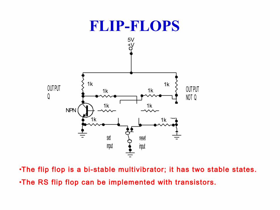
FLIP-FLOPS
OUT PUTQ
OUT PUTNOT Q
resetinput
setinput
+V5V
NPNNPN
1k1k
1k1k
1k1k
1k1k
•The f l ip f lop is a bi-stable mult ivibrator; i t has two stable states.
•The RS f l ip f lop can be implemented with transistors.

R-S FLIP-FLOP
Symbols:
Truth Table:
Set
Reset
S
R
Q
Q
Normal
Comple-mentary
FF
Mode of Operation Inputs Outputs
S R Q Q’
Prohibited 0 0 1 1 Set 0 1 1 0 Reset 1 0 0 1 Hold 1 1 Q Q’
NOTE: Active-LOW inputs
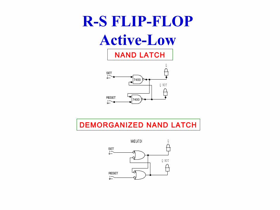
R-S FLIP-FLOPActive-Low
Q NOT
Q
RESET
SET
7400
7400
NAND LATCH
DEMORGANIZED NAND LATCH
NAND LAT CH Q
Q NOT
SET RES Q NOT -Q MODE 0 0 1 1 PROHIBIT ED 0 1 1 0 SET 1 0 0 1 RESET 1 1 NO CHG HOLD
RESET
SET
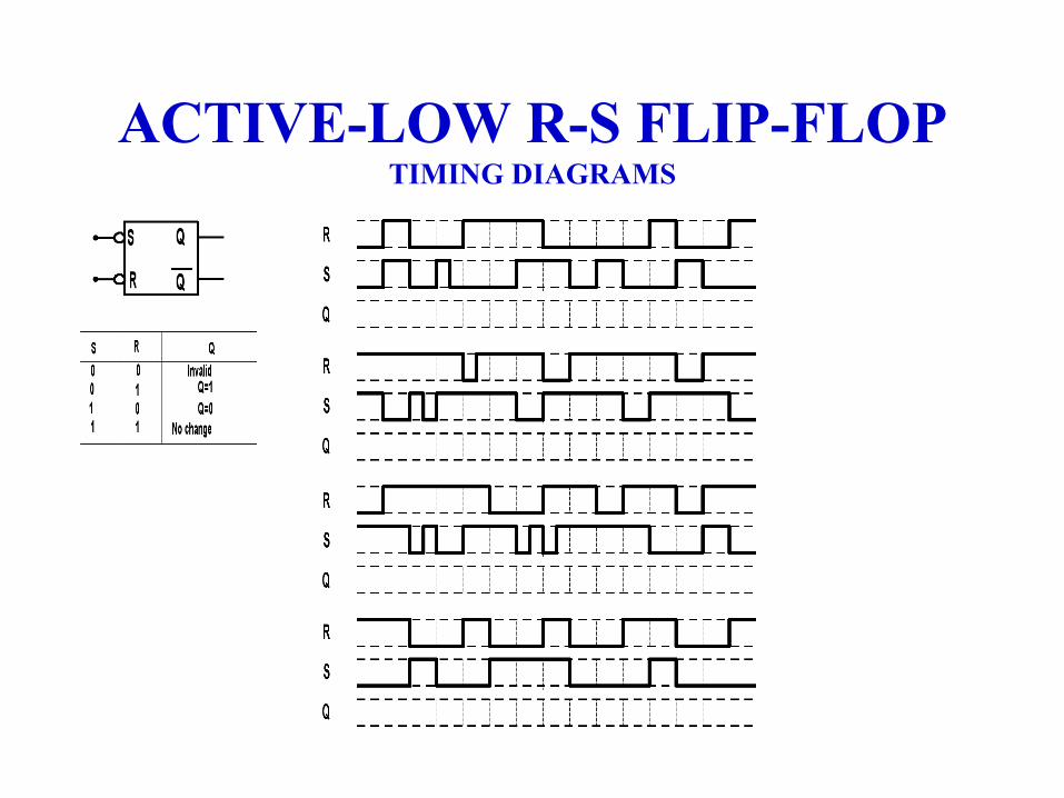
ACTIVE-LOW R-S FLIP-FLOPTIMING DIAGRAMS
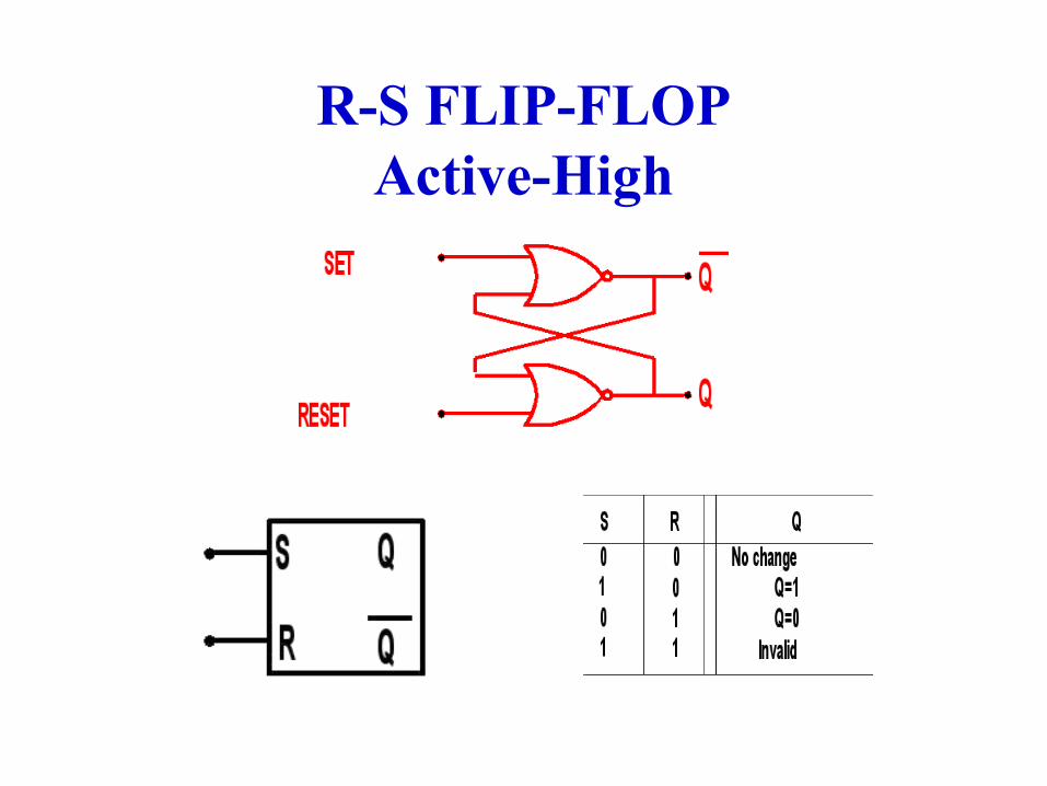
R-S FLIP-FLOPActive-High
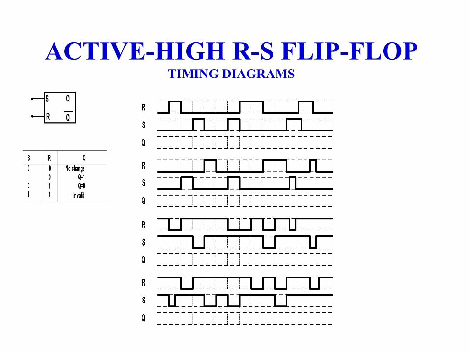
ACTIVE-HIGH R-S FLIP-FLOPTIMING DIAGRAMS
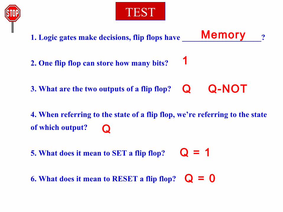
1. Logic gates make decisions, flip flops have ____________________?
2. One flip flop can store how many bits?
3. What are the two outputs of a flip flop?
4. When referring to the state of a flip flop, we’re referring to the state
of which output?
5. What does it mean to SET a flip flop?
6. What does it mean to RESET a flip flop?
TEST
Memory
1
Q Q-NOT
Q
Q = 1
Q = 0

What is the mode of operation of the R-S flip-flop (set, reset or hold)?What is the output at Q from the R-S flip-flop (active LOW inputs)?
Mode of operation = ?
?H
LLow
Reset
TEST
Mode of operation = ?
?L
H
Mode of operation = ?
?H
H
High
High
Hold
Set

CLOCKED R-S FLIP-FLOP
Set
Reset
S
R
Q
Q
FF
ASYNCHRONOUS
Outputs of logic circuit can change state anytime one or more input changes
Set
Reset
S
R
Q
Q
FF
ClockCLK
SYNCHRONOUS
Clock signal determines exact t ime at which any output can change state
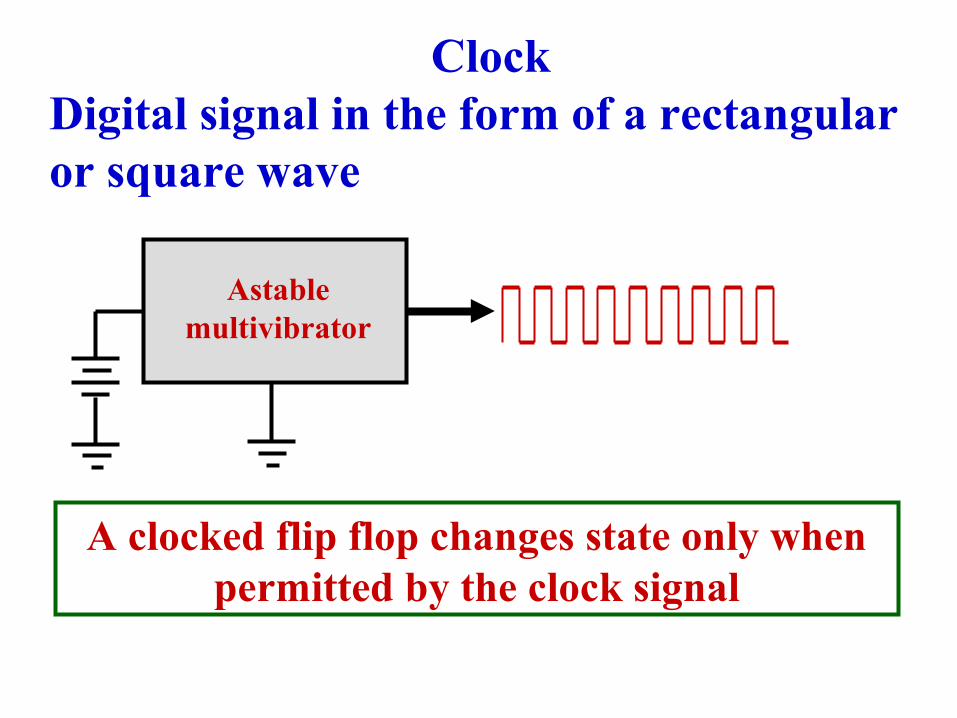
Astablemultivibrator
ClockDigital signal in the form of a rectangular or square wave
A clocked flip flop changes state only when permitted by the clock signal

TRIGGERING OF FLIP-FLOPS
• Level-triggering is the transfer of data from input to output of a flip-flop anytime the clock pulse is proper voltage level.
• Edge-triggering is the transfer of data from input to output of a flip-flop on the rising edge (L-to-H) or falling edge (H-to-L) of the clock pulse. Edge triggering may be either positive-edge (L-to-H) or negative-edge (H-to-L).
Level triggering
Positive-edge triggeringNegative-edge triggering
H
Ltime
NGT-Negative Going Transit ionPGT-Posit ive Going Transit ion

CLOCKED R-S FLIP-FLOP
Symbols:
Truth Table:Mode of operation Inputs Outputs
Clk S R Q Q’
Hold + pulse 0 0 no change Reset + pulse 0 1 0 1 Set + pulse 1 0 1 0 Prohibited 1 1 0 0
NOTE: Active-High inputs
Set
Reset
S
R
Q
Q
Normal
Comple-mentary
FF
ClockCLK
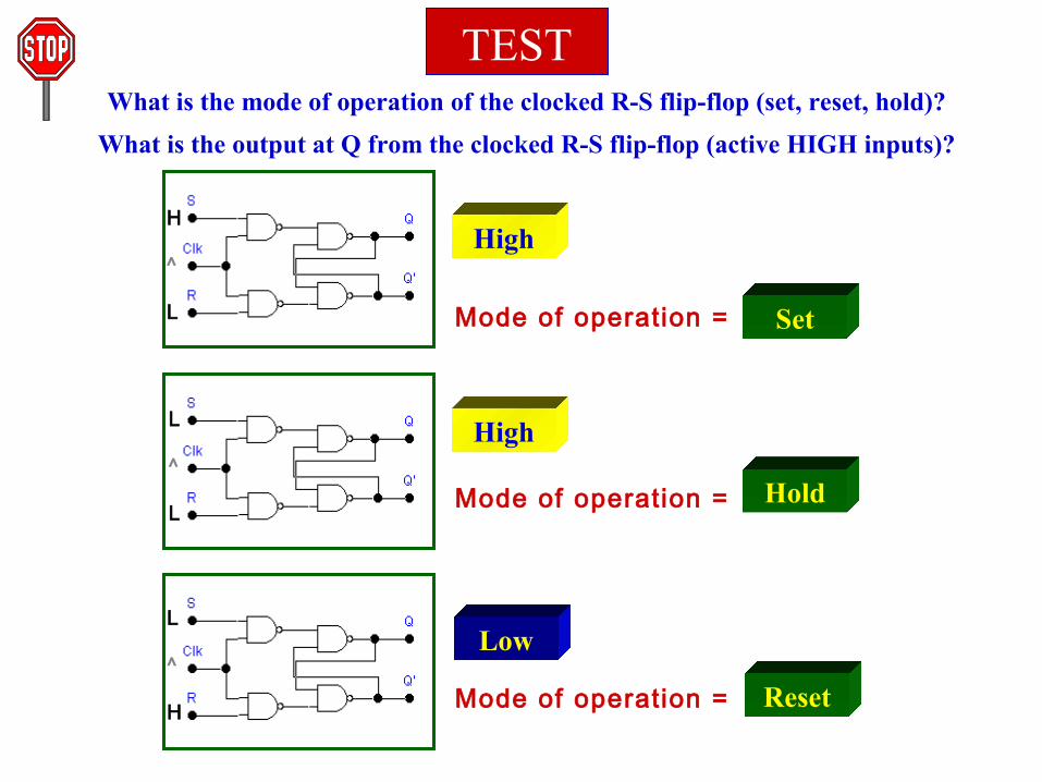
What is the mode of operation of the clocked R-S flip-flop (set, reset, hold)?
What is the output at Q from the clocked R-S flip-flop (active HIGH inputs)?
H
^
L Mode of operation = ?
?
L
^
L Mode of operation = ?
?
L
^
H Mode of operation = ?
?
High
Set
High
Low
Hold
Reset
TEST
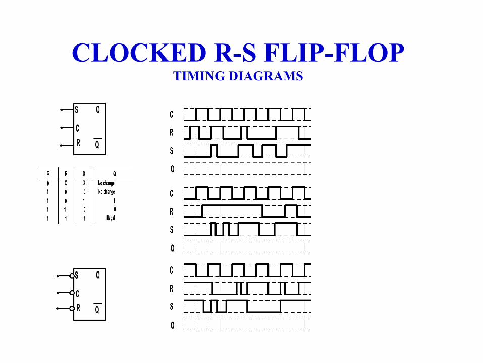
CLOCKED R-S FLIP-FLOPTIMING DIAGRAMS
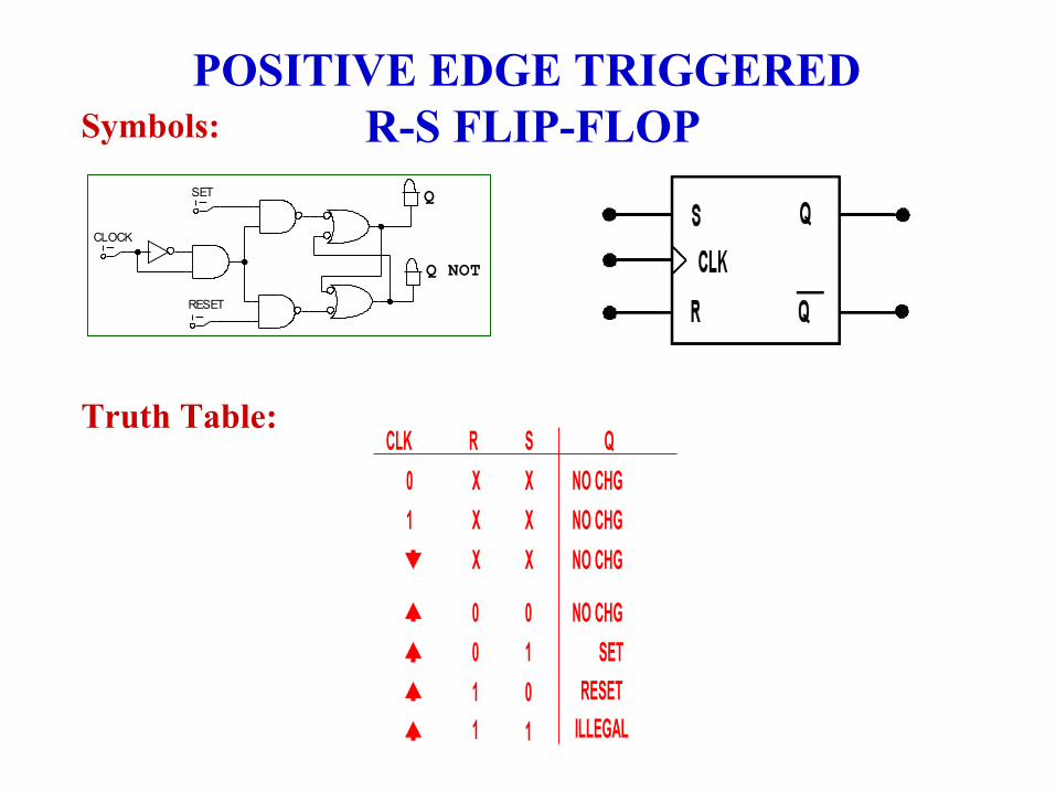
POSITIVE EDGE TRIGGERED R-S FLIP-FLOPSymbols:
Truth Table:
CLK SET RES Q NOT -Q MODE PGT 0 0 NO CHG HOLD PGT 0 1 0 1 RESET PGT 1 0 1 0 SET PGT 1 1 1 1 INVALID
Q NOT
Q
EDGE T RIGGERED R-S FLIP FLOPSET
RESET
CLOCK
CLK R S
0
Q
X X
1
NO CHG
X X
0
X
0
NO CHG
X NO CHG
0 NO CHG
1
1 0
1 1
SET
RESET
ILLEGAL
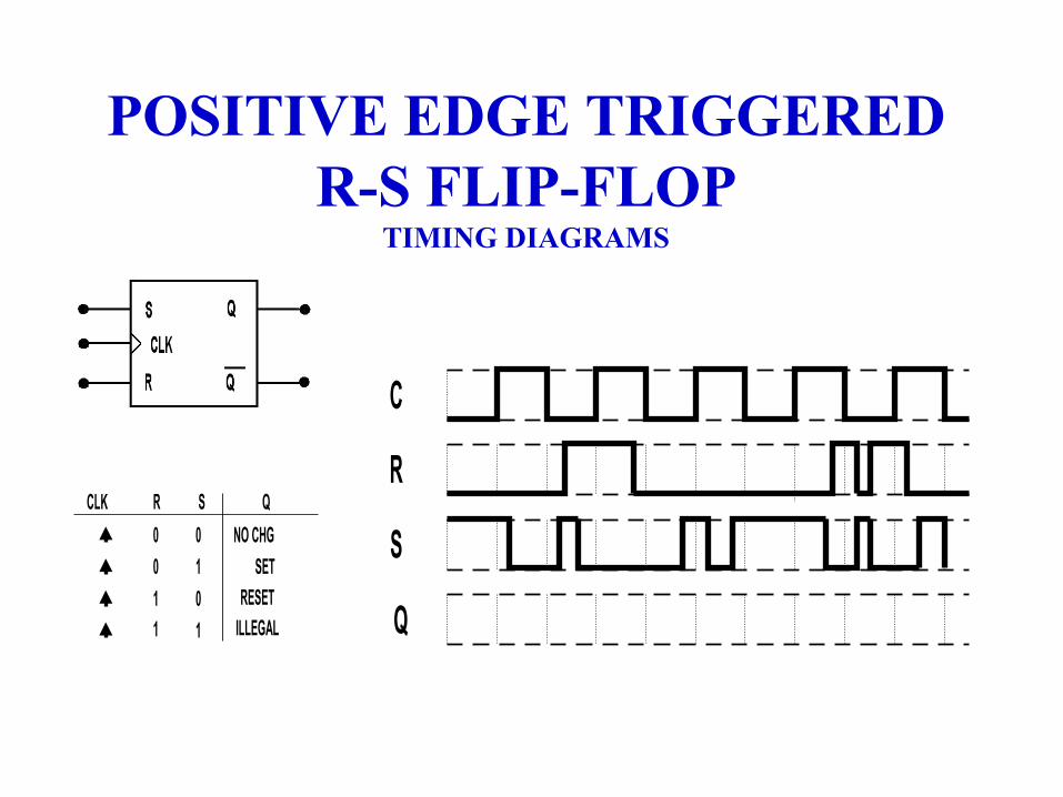
POSITIVE EDGE TRIGGEREDR-S FLIP-FLOP
TIMING DIAGRAMS
0
0
0 NO CHG
1
1 0
1 1
SET
RESET
ILLEGAL
CLK R S Q
C
R
S
Q
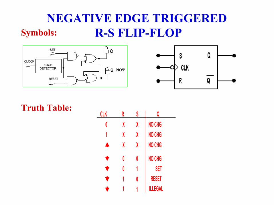
NEGATIVE EDGE TRIGGERED R-S FLIP-FLOPSymbols:
Truth Table:
CLK SET RES Q NOT -Q MODE PGT 0 0 NO CHG HOLD PGT 0 1 0 1 RESET PGT 1 0 1 0 SET PGT 1 1 1 1 INVALID
Q NOT
Q
EDGE T RIGGERED R-S FLIP FLOPSET
RESET
CLOCK
CLK R S
0
Q
X X
1
NO CHG
X X
0
X
0
NO CHG
X NO CHG
0 NO CHG
1
1 0
1 1
SET
RESET
ILLEGAL
EDGE DETECTOR
NEGATIVE EDGE TRIGGEREDR-S FLIP-FLOP
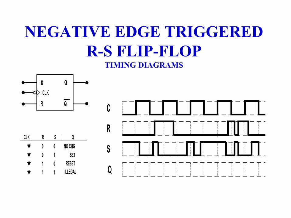
TIMING DIAGRAMS
0
0
0 NO CHG
1
1 0
1 1
SET
RESET
ILLEGAL
CLK R S Q
C
R
S
Q

TEST
1. Type of flip flop where the outputs of circuit can change state anytime
one or more input changes? ASYNCHRONOUS
2. Type of flip flop where the clock signal controls when any output can
change state? SYNCHRONOUS
3. What do we call a digital signal in the form of a repetitive pulse or square wave?
CLOCK
4. Which is easier to design and troubleshoot, clocked or not clocked flip flops?
Clocked f l ip f lops are easier to troubleshoot because we can stop the clock and examine one set of input and output condit ions.