1.3318261 EB CNT Graphene
71
Ion and electron irradiation-induced effects in nanostructured materials A. V. Krasheninnikov and K. Nordlund Citation: Journal of Applied Physics 107, 071301 (2010); doi: 10.1063/1.3318261 View online: http://dx.doi.org/10.1063/1.3318261 View Table of Contents: http://scitation.aip.org/content/aip/journal/jap/107/7?ver=pdfcov Published by the AIP Publishing [This article is copyrighted as indicated in the abstract. Reuse of AIP content is subject to the terms at: http://scitation.aip.org/termsconditions. Downloaded to ] IP: 115.78.224.101 On: Fri, 15 Nov 2013 02:14:06
-
Upload
pham-thi-thu-hong -
Category
Documents
-
view
26 -
download
4
Transcript of 1.3318261 EB CNT Graphene

Ion and electron irradiation-induced effects in nanostructured materialsA. V. Krasheninnikov and K. Nordlund Citation: Journal of Applied Physics 107, 071301 (2010); doi: 10.1063/1.3318261 View online: http://dx.doi.org/10.1063/1.3318261 View Table of Contents: http://scitation.aip.org/content/aip/journal/jap/107/7?ver=pdfcov Published by the AIP Publishing
[This article is copyrighted as indicated in the abstract. Reuse of AIP content is subject to the terms at: http://scitation.aip.org/termsconditions. Downloaded to ] IP:
115.78.224.101 On: Fri, 15 Nov 2013 02:14:06

APPLIED PHYSICS REVIEWS
Ion and electron irradiation-induced effects in nanostructured materialsA. V. Krasheninnikov1,2,a� and K. Nordlund1,b�
1Department of Physics, University of Helsinki, P.O. Box 43, Helsinki FI-00014, Finland2Department of Applied Physics, P.O. Box 1100, FI-00076 Aalto University, Finland
�Received 22 July 2009; accepted 18 January 2010; published online 6 April 2010�
A common misconception is that the irradiation of solids with energetic electrons and ions hasexclusively detrimental effects on the properties of target materials. In addition to the well-knowncases of doping of bulk semiconductors and ion beam nitriding of steels, recent experiments showthat irradiation can also have beneficial effects on nanostructured systems. Electron or ion beamsmay serve as tools to synthesize nanoclusters and nanowires, change their morphology in acontrollable manner, and tailor their mechanical, electronic, and even magnetic properties.Harnessing irradiation as a tool for modifying material properties at the nanoscale requires havingthe full microscopic picture of defect production and annealing in nanotargets. In this article, wereview recent progress in the understanding of effects of irradiation on various zero-dimensional andone-dimensional nanoscale systems, such as semiconductor and metal nanoclusters and nanowires,nanotubes, and fullerenes. We also consider the two-dimensional nanosystem graphene due to itssimilarity with carbon nanotubes. We dwell on both theoretical and experimental results and discussat length not only the physics behind irradiation effects in nanostructures but also the technicalapplicability of irradiation for the engineering of nanosystems. © 2010 American Institute ofPhysics. �doi:10.1063/1.3318261�
TABLE OF CONTENTS
I. INTRODUCTION. . . . . . . . . . . . . . . . . . . . . . . . . . . . 2A. Scope of the review. . . . . . . . . . . . . . . . . . . . . 3B. Organization of the paper. . . . . . . . . . . . . . . . . 3
II. PRODUCTION OF DEFECTS IN SOLIDSUNDER ION AND ELECTRON IRRADIATION.. 4
A. Production of defects in bulk targets. . . . . . . . 4B. Creation of defects in nanoscale materials
under irradiation. . . . . . . . . . . . . . . . . . . . . . . . 5III. EXPERIMENTAL TECHNIQUES USED TO
IDENTIFY DEFECTS INNANOSTRUCTURED MATERIALS. . . . . . . . . . . 6
IV. COMPUTATIONAL ATOMISTIC METHODSUSED FOR MODELING IRRADIATIONEFFECTS IN SOLIDS. . . . . . . . . . . . . . . . . . . . . . . 7
A. Binary collision approximation-basedmethods. . . . . . . . . . . . . . . . . . . . . . . . . . . . . . . 8
B. Molecular dynamics with empiricalpotentials. . . . . . . . . . . . . . . . . . . . . . . . . . . . . . 8
C. Simulation setup. . . . . . . . . . . . . . . . . . . . . . . . 8D. Density functional theory-based methods. . . . 9E. Tight-binding methods. . . . . . . . . . . . . . . . . . . 9F. Time-dependent DFT simulations. . . . . . . . . . 10G. Phenomenological descriptions of electronic
excitation. . . . . . . . . . . . . . . . . . . . . . . . . . . . . . 10
H. Kinetic Monte Carlo approach. . . . . . . . . . . . . 11I. Summary of simulation methods and their
limitations. . . . . . . . . . . . . . . . . . . . . . . . . . . . . 11V. IRRADIATION EFFECTS IN CARBON
NANOSYSTEMS. . . . . . . . . . . . . . . . . . . . . . . . . . . . 12A. Defect production in carbon nanosystems
under irradiation. . . . . . . . . . . . . . . . . . . . . . . . 121. Production of defects in SWNTs under
ion irradiation. . . . . . . . . . . . . . . . . . . . . . . . 122. Production of defects in multiwalled and
bundled-up nanotubes. . . . . . . . . . . . . . . . . 143. Ion irradiation of fullerenes and
fullerene-nanotube systems. . . . . . . . . . . . . 144. Simulations of electron irradiation of
carbon nanosystems. . . . . . . . . . . . . . . . . . . 155. Carbon atom displacement energy. . . . . . . 15
B. Irradiation-induced defects in carbonnanosystems and their properties. . . . . . . . . . . 161. Vacancies in graphene and carbon
nanotubes. . . . . . . . . . . . . . . . . . . . . . . . . . . 172. Carbon adatoms as interstitials in
single-walled carbon nanotubes. . . . . . . . . 193. Carbon adatoms on graphene. . . . . . . . . . . 194. Stone-Wales defects. . . . . . . . . . . . . . . . . . . 195. Irradiation-induced defects in MWNTs
and nanotube bundles. . . . . . . . . . . . . . . . . 206. Annealing of irradiation-induced defects.. 207. Relationship between point defects in
nanotubes, those in multilayer graphene,and those in graphite. . . . . . . . . . . . . . . . . . 22
a�Electronic mail: [email protected]�Electronic mail: [email protected].
JOURNAL OF APPLIED PHYSICS 107, 071301 �2010�
0021-8979/2010/107�7�/071301/70/$30.00 © 2010 American Institute of Physics107, 071301-1
[This article is copyrighted as indicated in the abstract. Reuse of AIP content is subject to the terms at: http://scitation.aip.org/termsconditions. Downloaded to ] IP:
115.78.224.101 On: Fri, 15 Nov 2013 02:14:06

C. Electron irradiation of carbon nanostructures.. 221. Electron irradiation of graphene. . . . . . . . . 232. Electron irradiation of freestanding
single-walled carbon nanotubes. . . . . . . . . 233. Irradiation-induced links between
single-walled carbon nanotubes inbundles. . . . . . . . . . . . . . . . . . . . . . . . . . . . . 24
4. Electron irradiation of multiwalledcarbon nanotubes. . . . . . . . . . . . . . . . . . . . . 24
5. Welding and coalescence of carbonnanotubes under electron beam. . . . . . . . . . 25
6. Engineering carbon nanostructures with afocused electron beam. . . . . . . . . . . . . . . . . 26
D. Ion irradiation of carbon nanomaterials. . . . . . 281. Ion irradiation of graphene. . . . . . . . . . . . . 282. Experiments on heavy ion irradiation of
carbon nanotubes. . . . . . . . . . . . . . . . . . . . . 29a. High-dose irradiation. . . . . . . . . . . . . . . . 29b. Low-dose irradiation. . . . . . . . . . . . . . . . 32
3. Light ions: Proton irradiation of carbonnanotubes. . . . . . . . . . . . . . . . . . . . . . . . . . . 33
4. Welding of nanotubes by ion beams. . . . . . 345. Ion-irradiation-induced links between
nanotubes and substrates. . . . . . . . . . . . . . . 346. Irradiation-mediated doping of carbon
nanotubes with foreign atoms. . . . . . . . . . . 347. Carbon nanotubes as masks against ion
irradiation. . . . . . . . . . . . . . . . . . . . . . . . . . . 358. Channeling of ions in nanotubes. . . . . . . . . 35
E. Irradiated carbon nanotubes and onions ashigh-pressure cells. . . . . . . . . . . . . . . . . . . . . . 36
F. Influence of defects on the properties ofnanocarbon systems. . . . . . . . . . . . . . . . . . . . . 381. Mechanical properties. . . . . . . . . . . . . . . . . 382. Electronic properties. . . . . . . . . . . . . . . . . . 393. Magnetic properties. . . . . . . . . . . . . . . . . . . 40
VI. IRRADIATION EFFECTS IN BORONNITRIDE �BN� NANOSYSTEMS. . . . . . . . . . . . . 40A. Electron irradiation. . . . . . . . . . . . . . . . . . . . . . 40B. Ion irradiation. . . . . . . . . . . . . . . . . . . . . . . . . . 41C. Theory of point defects in BN nanotubes. . . . 42D. Boron and nitrogen atom displacement
energies. . . . . . . . . . . . . . . . . . . . . . . . . . . . . . . 43E. Engineering boron nitride nanosystems with
the electron beam. . . . . . . . . . . . . . . . . . . . . . . 44VII. EFFECTS OF IRRADIATION ON
NANOWIRES �NWS�. . . . . . . . . . . . . . . . . . . . . . 45A. Silicon-based NWs. . . . . . . . . . . . . . . . . . . . . . 45B. Implantation of compound semiconductor
NWs. . . . . . . . . . . . . . . . . . . . . . . . . . . . . . . . . 46C. Electron beam modification. . . . . . . . . . . . . . . 47D. Ion beam synthesis of NWs. . . . . . . . . . . . . . . 49E. Ion tracks and NWs. . . . . . . . . . . . . . . . . . . . . 50F. Simulation of radiation effects in NWs. . . . . . 50
VIII. IRRADIATION EFFECTS INFREESTANDING NANOCLUSTERS. . . . . . . . . 51A. Sputtering of nanoparticles. . . . . . . . . . . . . . . . 51B. Sputtering of nanoparticles by swift heavy
ions. . . . . . . . . . . . . . . . . . . . . . . . . . . . . . . . . . 52
C. Phase changes in nanoparticles. . . . . . . . . . . . 53D. Irradiation of quantum dots. . . . . . . . . . . . . . . 55
1. InAs quantum dots. . . . . . . . . . . . . . . . . . . . 552. Other quantum dots. . . . . . . . . . . . . . . . . . . 55
IX. IRRADIATION EFFECTS IN EMBEDDEDNANOCLUSTERS �NCS�. . . . . . . . . . . . . . . . . . . . 56A. Effects of radiation on embedded NCs. . . . . . 56
1. Si and Ge NCs in silica. . . . . . . . . . . . . . . . 562. Metal NCs. . . . . . . . . . . . . . . . . . . . . . . . . . 573. Inverse Ostwald ripening. . . . . . . . . . . . . . . 58
B. Elongation of nanoclusters by swift heavyions. . . . . . . . . . . . . . . . . . . . . . . . . . . . . . . . . . 58
X. CONCLUSIONS AND OUTLOOK. . . . . . . . . . . . . 60APPENDIX: WIKIPEDIA ARTICLES RELATEDTO THE TOPIC. . . . . . . . . . . . . . . . . . . . . . . . . . . . . . . 61
I. INTRODUCTION
Irradiation of solids with energetic particles, such aselectrons or ions, normally gives rise to formation of atomicdefects in the target and spoils the material properties. His-torically, the necessity to understand the irradiation-induceddegradation of metal and graphitic components of fissionand, later on, fusion reactors was the initial driving force forstudying effects of irradiation on solids.1–3
However, in spite of the damage, irradiation may overallhave a beneficial effect on the target. A good example is theindustrially very important ion implantation ontosemiconductors.4 This application motivated further studiesof defect production under irradiation because each im-planted atom creates many lattice defects in the sample.5
Another important example of a positive effect of irradiationcoming from biophysics is the radiation-assisted treatment ofcancer.
It has been demonstrated that irradiation, especiallywhen combined with heat treatment, can also have beneficialeffects on nanostructured materials. Experiments carried outfor the technologically important carbon nanomaterials, suchas nanotubes and graphene, showed that their atomic struc-ture and morphology can be changed in a controllable man-ner by irradiation.6–16 Besides, it was demonstrated thatnanotubes can be interconnected or merged9,12,17,18 and thatirradiation can give rise to many interesting phenomena,such as extreme pressure inside nanotubes19 or fullerenelike“onions,”6,20 so that these systems can be used as nanolabo-ratories for studying pressure-induced transformations at thenanoscale. Furthermore, recent experiments indicate thation,21–38 electron,6,39–52 and high energy photon53–56 irradia-tion can be used to tailor the mechanical,8,10
electronic,11,21–23 and even magnetic57,58 properties of nano-structured carbon materials.
Examples of irradiation-assisted manipulation of noncar-bon nanoscale materials are the patterning or ordering of themagnetic properties of ultrathin ferromagnetic films,59,60 fab-rication of nanodots61 and silicon carbide clusters,62 the self-organization of ensembles of embedded nanoclusters due tothe inverse Ostwald ripening effect,63 the transformation ofspherical nanocolloids into ellipsoids with the aim to build a
071301-2 A. V. Krasheninnikov and K. Nordlund J. Appl. Phys. 107, 071301 �2010�
[This article is copyrighted as indicated in the abstract. Reuse of AIP content is subject to the terms at: http://scitation.aip.org/termsconditions. Downloaded to ] IP:
115.78.224.101 On: Fri, 15 Nov 2013 02:14:06

photonic crystal,64 doping of Si nanowires �NWs�,65 or thecreation of metallic nanoparticles in dielectric matrices,64
just to mention a few.Irradiation of nanostructures may give rise to quite un-
expected and even counterintuitive results. For example, or-dering of fullerene and carbon nanotube thin films underhigh energy ion irradiation �200 MeV Au and 60 MeV Niions� has been reported,66 probably due to effects of ion-beam heating and a vanishingly small probability for defectproduction in a very thin target. Thus, harnessing irradiationas a tool for improving the properties of nanomaterials re-quires full microscopic understanding of such phenomena asdefect production in nanoscale systems under irradiation,damage accumulation and annealing, as well as the knowl-edge of how the defects affect the material properties. Al-though various experimental techniques can be used to char-acterize defects, the vast majority of experiments are carriedout ex situ. An exception is the transmission electron micros-copy �TEM�, which makes it possible to not only create de-fects, but also visualize them in situ. However, even TEMcannot give any information on the defect creation process,as it occurs on the picosecond time scale. At the same time,atomistic computer simulations have provided lots of insightinto irradiation damage creation in bulk metals and semicon-ductors, as well as in nanostructures, as such simulationsallow one not only to calculate the characteristic of the ma-terials with defects, but also to model the defect productionin real time. Recently, substantial progress in understandingthe irradiation effects and properties of defects in variousnanomaterials was achieved. This was possible in part due tothe advent of high-performance computers, which stimulatedthe development of computational tools for realistic simula-tions of nanostructured systems.
A. Scope of the review
In this review, we give a summary of the most recentexperimental results on irradiation effects in various zero-dimensional �0D� and one-dimensional �1D� nanoscale sys-tems, such as semiconductor and metal clusters and NWs,nanotubes, and fullerenes. We also consider the two-dimensional �2D� nanosystem graphene due to its similaritywith carbon nanotubes. We restrict our consideration to se-lected papers reporting results of irradiation with ions orelectrons and do not review effects of neutron or photonirradiation and also consider irradiation of bulk materialswith nanoclusters to fall outside the scope of the current re-view, although this certainly also is a very interesting topic�see, e.g., Refs. 67–71�.
Due to the success of atomistic simulations in gettinginsights into irradiation-induced phenomena in nanomateri-als, we also give an overview of recent computational workand the simulation methods used. We discuss at length notonly the physics behind irradiation of nanostructures but alsothe technical applicability of irradiation for nanoengineeringof nanosystems. We stress that although several review ar-ticles on the subject focused on carbon nanosystems,72–74 ionimplantation onto nanomaterials,75 atomistic simulations ofirradiation effects,76,77 and focused electron/ion beams78
have recently been published, the field has been developingquite fast following the discoveries of new important nano-materials, such as graphene,79,80 which motivates reanalyzingand reviewing the literature.
To quantify the growth of the field, we carried out a Webof Science81 search on irradiation effects and 0D or 1D nano-structures, see Fig. 1. The results show that both the numberof publications and their impact, as measured in the numberof citations, are in a strong and continued growth.
B. Organization of the paper
The paper is organized as follows. In Sec. II, we brieflyreview the well-established basic aspects of interaction ofenergetic particles—electrons and ions with kinetic energiesclearly above thermal ones—with bulk and nanoscale targets.A short overview of the experimental tools, which can beused to detect and characterize native and irradiation-induceddefects in nanostructures, is given in Sec. III. Computationaltechniques used for simulations of defect production in bulkand nanomaterials under irradiation are discussed in Sec. IV.We stress that simulations of irradiation effects in solids re-quire modifications of the conventional molecular dynamics�MD� and electronic structure calculations algorithms, sothat we pay particular attention to the technical issues impor-tant for modeling electron and ion bombardment. In Sec. V,we dwell on irradiation effects in carbon nanomaterials. Wediscuss at length production of defects in carbon nanosys-tems under ion and electron irradiation, analyze the structureand properties of the most prolific irradiation-induced de-fects, and give an overview of the most interesting examplesof engineering the structure and properties of carbon nano-materials with electron and ion beams. Irradiation effects inBN nanosystems, which are closely related to carbon nano-materials, are reviewed in Sec. VI. The bombardment ofsemiconductor and metal NWs with energetic ions and elec-trons is discussed in Sec. VII, and irradiation effects in free-standing and embedded clusters are discussed in Secs. VIIIand IX.
0
100
200
300
400
500
600
Num
ber
ofpu
blic
atio
ns/y
ear
0
1000
2000
3000
4000
5000
6000
7000
Num
ber
ofci
tatio
ns/y
ear
1992 1994 1996 1998 2000 2002 2004 2006 2008Year
PublicationsCitations
FIG. 1. �Color online� Results of a Web of Science �Ref. 81� search carriedout on January 6, 2010, using the advanced search keyword “TS= �irradiation or implantation or collision cascade or radiation effects�AND TS= �nanocluster or NC or nanoparticle or NW or nanotube�.”Web of Science covers the titles, keywords, and abstracts of all major ref-ereed publication series in the natural sciences since 1949. The search gaveno hits before 1993. The strong and continued growth of the field and itsimpact �number of citations� is obvious from the graph.
071301-3 A. V. Krasheninnikov and K. Nordlund J. Appl. Phys. 107, 071301 �2010�
[This article is copyrighted as indicated in the abstract. Reuse of AIP content is subject to the terms at: http://scitation.aip.org/termsconditions. Downloaded to ] IP:
115.78.224.101 On: Fri, 15 Nov 2013 02:14:06

II. PRODUCTION OF DEFECTS IN SOLIDS UNDERION AND ELECTRON IRRADIATION
A. Production of defects in bulk targets
When an energetic particle—ion or electron—penetratesa solid, it collides with the nuclei and the electrons of thetarget, so that the projectile energy is transferred to the targetatoms. Although the low-energy �eV or keV� incoming ionsare quickly neutralized by capturing electrons from thetarget,82 in what follows, the incoming ion or atom is alwaysreferred to as “ion” to differentiate between the projectileand recoil atoms. If the target recoil atom acquires kineticenergy enough to leave its position in the atomic network,various atomic-scale defects may appear in the target. Manyof the point defects, e.g., vacancy-interstitial pairs, disappearimmediately after the impact �on the picosecond time scale�,but some defects may remain in the system or form morecomplicated defect structures.
The slowing down of an energetic ion moving in a solidtarget can be separated into two different mechanisms:83,84
electronic and nuclear stopping. The nuclear stopping origi-nates from ballistic collisions between the ion and the nucleiof atoms in the target, so that the ion kinetic energy is partlytransmitted to a target atom as a whole, resulting in its trans-lational motion. The energy loss is determined by screenedCoulomb interactions and momentum transfer. A commonfeature for all ions is that the nuclear stopping is dominantonly for relatively slow �Ekin�100 keV /amu� ions. Thenuclear collisions at higher energies usually occur as a se-quence of independent binary collisions of atoms, betweenwhich the ion moves in an almost straight path, and its en-ergy loss is predominantly by electronic stopping. For theconcept of independent collisions to be meaningful, the dis-tances between successive collisions need to be at least abouttwo interatomic spacings, i.e., �5 Å. In this initial stage of acascade, the system is not thermodynamic at all since theatomic motion occurs much faster than the thermodynamicrelaxation time scale of atoms �which is of the order of 100fs or more�. Once the ion has lost enough energy, or if sev-eral recoils happen to occur close to each other, numerouscollisions may occur in close vicinity of each other. In thiscase, the binary collision concept does not work any more,but the cascade becomes a complex many-body phenom-enon, which leads to the complete breakup of the lattice. Dueto the high kinetic energy of the recoils, the region of over-lapping collisions can in some sense be considered to be“hot”85–88 and is hence called a “heat spike” or “thermalspike.” In bulk materials, this hot region cools down rapidlydue to heat conduction to the surrounding lattice. Heat spikescan become important for heavy projectiles in dense materi-als.
The electronic stopping is governed by inelastic colli-sions between the moving ion and the electrons in the target,which can be either bound or free. Many different physicalprocesses contribute to the electronic stopping: ionization ofthe target atoms, excitation of electrons into the conductionband, collective electronic excitations such as plasmons,etc.89–102
Electronic stopping dominates at high ion energies �seeFig. 2�. The crossover between the nuclear and electron stop-ping depends on the ion mass �in case of a carbon target 100keV for Ar ions and 1 MeV for Xe�. For hydrogen ions�protons�, electronic stopping always dominates.
Due to the different mechanisms of conversion of elec-tronic excitations into heat, the electronic structure of thetarget strongly affects the outcome of the ion impact. In met-als, the electronic excitations are delocalized due to the pres-ence of conduction electrons. This makes the excitations lesslikely to lead to atom motion, so that radiation damagecomes mostly from knock-on atom displacements.
In insulators �e.g., diamond103 or silica64�, above a cer-tain electronic energy deposition threshold,104 excitationsmay result in a strong heating of the lattice and damage by acylindrical form of heat spikes.105 To reach this depositionregime requires high energy �tens of MeV or more� heavyion irradiation, whence the regime is called “swift heavy ionirradiation.” Swift heavy ions can give rise to so-called“tracks”—amorphous regions that appear along the trajec-tory of the high energy ion. The same effect has been ob-served in fullerenes.106 Normally the tracks are well alignedwith respect to the beam directions and themselves can beviewed as nanostructures inside bulk materials. The trackcores can be etched away and filled with some other mate-rial, which enables production of long straight NWs. Thetracks may also have an internal structure, being underdensein the center and overdense in the surroundings, at least insilica.107
As for electron irradiation, energetic electrons interactwith the nuclei and the electron system in the target.72 Be-cause of momentum conservation, only a small fraction ofthe impinging electron energy can be transferred to anucleus, so that a rather high electron energy �“thresholdenergy”� is needed to displace an atom. The energy transferoccurs via electron-nucleus scattering. For example, an elec-tron energy of 100 keV is needed to transfer approximately20 eV to a carbon atom. This is close to the threshold for
0 1000 2000 3000 4000Ion energy (keV)
0
1
2
3
Stoppingpower(keV/nm)
Xe, electr.Xe, nucl.Ar, electr.Ar, nucl.H, electr.H, nucl.
FIG. 2. �Color online� Electronic and nuclear stopping power as a functionof ion energy for H, Ar, and Xe ions moving in a C target, as calculatedwithin the Ziegler–Biersack–Littmark �Ref. 83� formalism. At low ion en-ergies, the nuclear stopping prevails, except for very light ions such as Hand He.
071301-4 A. V. Krasheninnikov and K. Nordlund J. Appl. Phys. 107, 071301 �2010�
[This article is copyrighted as indicated in the abstract. Reuse of AIP content is subject to the terms at: http://scitation.aip.org/termsconditions. Downloaded to ] IP:
115.78.224.101 On: Fri, 15 Nov 2013 02:14:06

displacing the atom from the lattice site in a graphitic struc-ture. Electron-electron scattering, on the other hand, is al-ready possible at low electron energies and may cause ion-ization or bond breaking. This kind of energy transfer doesnot normally lead to atom displacements but may damage thetarget due to beam-stimulated local chemical reactions.108–111
The cross sections of both nuclear and electron scatteringdecreases with increasing electron energy.
Both electron and ion beams can be focused onto an areaof several nanometers �and even down to 0.6 Å in someTEMs�, which makes it possible to create defects in prede-termined areas of the sample. We stress that even at themaximum currents available �for highly focused electronbeams, currents in a TEM can be about 105 A cm−2 so that100 displacement per carbon atom can be achieved�, thetypical time between the impacts of the particles onto thesame area is normally much longer than the typical timeduring which the extra energy is dissipated into the environ-ment, so that one can neglect temporal correlations betweencollision cascades, and consider the initial damage from im-pacts of energetic particles “one by one.”
The effects of an ion or electron impact on a materialmay extend beyond the region of initial collisions due toseveral physical effects. The defects �both point and ex-tended ones� produced during the irradiation can, unless theyrecombine during the cascade development with each other,migrate in principle arbitrarily far in the sample. A cascademay also “raise” impurities from essentially immobile posi-tions into mobile ones.
The electronic stopping power can excite electrons torelatively high �keV� energies,112 and such electrons �knownoften as � electrons� can travel far in the lattice. This can atleast in principle produce damage far from the nuclear colli-sion region and is certainly a significant factor behind trans-porting electron excitation energy away from the central re-gion of a swift heavy ion track.113,114 It is also well knownthat nuclear collision cascades, especially in the heat spikeregime, also induce a sound/shock wave in thematerials.115,116 Such a shock wave can in principle causeemission of material far away from the impact site, althoughin practice this is likely to occur if the material is in anunstable state to begin with.115 More likely is the situation ofthe pressure wave or long-term stress relaxation causingplastic deformation of the material outside, also far from theregion of atomic collisions.117
Any kind of irradiation can also generate phonons. Thesehave relatively low energies and are thus unlikely to causeany materials modification. However, it has been proposedthat anharmonic longitudinal vibrations, so called “discretebreathers,” can dramatically enhance N atom migration insteels.118
Electronic excitations associated with irradiation cannaturally also cause photon emission when the electrons de-cay to lower-energy states. In materials with a band gap, thephotons can travel far from the impact site. It is very unlikelythat such photons could cause significant damage to the ma-terial as they are emitted in random directions and the radia-tion intensity decays rapidly with distance. However, the
light emission, known as ionoluminescence, may be usefulas a source of information during ion beam analysis ofmaterials.119
Near surfaces, all of the processes described in this sec-tion can lead to sputtering. Linear cascades produce sputter-ing if a recoil is backscattered through the surface. Heatspikes can lead to massive sputtering yields by a combina-tion of evaporation and flow of liquid material from the heatspike.68,120 Low-energy can also sputter material at energiesbelow the physical sputtering threshold via bond-weakeningand breaking mechanisms.121 Well-described examples ofthis are the so called Küppers cycle, in which ion bombard-ment weakens chemical bonds so that molecules can thendesorb thermally122 and swift chemical sputtering, in whichhydrogen isotopes with energies of the order of 10 eV canbreak bonds athermally by entering between twoatoms.123–125 Swift heavy ions can also cause massive sput-tering via the heat spikes induced in them.126 Electron irra-diation can naturally lead to sputtering if the kinetic energytransfer from the electron to sample atoms is above thethreshold energy for sputtering. Also much lower energyelectrons can lead to sputtering of insulators via promotionof electrons in chemical bonds to antibonding states.127
The typical time scale for defect production and sputter-ing is as follows. An energetic electron transfers energy to anucleus essentially instantly �for 10−21 s, Ref. 72�, and simi-larly most of the transfer of electronic energy from swiftheavy ions to sample atoms via electron-phonon coupling�EPC� occurs on time scales less than 10 fs.128 The ballisticphase of a collision cascade after an impact of an electron orion takes of the order of 100 fs, after which a heat spike mayform in dense materials. The “extra” energy brought in bythe energetic particle is, for all kinds of irradiations, dissi-pated to the surroundings �either by heat conduction or nearsurfaces also by sputtering� on nanosecond time scales, afterwhich defects are formed. These defects would be fullystable at 0 K, but may, at finite temperatures, start migratingand thus recombining or forming larger defect complexes oradatoms on surfaces.129
The relatively short time scale of defect creation makesdynamic atomistic simulation of defect production feasible.The thermal annealing of defects occurs on a macroscopictime scale, so that special techniques such as accelerated130
and parallel replica131 MD or kinetic Monte Carlo �KMC�approaches132 should be used.
B. Creation of defects in nanoscale materials underirradiation
Production of defects in irradiated nanosystems is differ-ent from that in bulk materials. This is due to a small systemsize in one or more dimensions, which affects the dissipationof energy brought in by the energetic particle. An illustrationof the difference in energy distribution between a three-dimensional �3D� and 1D system is presented in Fig. 3 bysnapshots of atom kinetic energy profiles �“temperature”134�taken several femtoseconds after the ion impacts. The re-duced dimensionality may give rise to a higher local kineticenergy after the impact so that the local temperature mayexceed the melting temperature of the material. This is par-
071301-5 A. V. Krasheninnikov and K. Nordlund J. Appl. Phys. 107, 071301 �2010�
[This article is copyrighted as indicated in the abstract. Reuse of AIP content is subject to the terms at: http://scitation.aip.org/termsconditions. Downloaded to ] IP:
115.78.224.101 On: Fri, 15 Nov 2013 02:14:06

ticularly important for zero-dimensional objects. For ex-ample, only Et=30 eV transferred to an atom in an isolatedfullerene C60 will raise temperature to T��1 /3Et /kB /60�2000 K, where kB is the Boltzmann constant, and an ad-ditional factor of 0.5 was introduced due to the equipartitiontheorem.
Three other important points should be taken into ac-count, which are as follows: �1� a big surface area of nano-systems results in a high sputtering yield, including sidewardand forward sputtering;135 �2� high surface-to-volume ratiomay also give rise to enhanced annealing; and �3� at highenergies of impinging particles normally only a small part ofthe projectile energy is deposited onto the nanosystem, con-trary to the case of irradiation of bulk systems when all theenergy is eventually dispersed in the sample. This is relatedto a drop in the cross section for defect production at highenergies of the particle.74 Correspondingly, the total amountof damage to a nanoscale object decreases with the particleenergy, contrary to the situation in bulk solids.
For ion irradiation, the application of the conventionaltheory of ion stopping to nanosystems is somewhat question-able, as the theory is based on averaging over many colli-sions of the projectile with the target atoms, which is obvi-ously incorrect for nano-objects. Besides this, theconventional separation of the ion energy loss into two com-ponents ignores the possible correlation between hardnuclear collisions and inelastic losses due to electronic exci-tations, which may be particularly important for nano-objects. The conventional approach to ion-nanosystem inter-actions has been demonstrated to be inadequate in certaincases for fullerenes136 and very thin targets,83 or at least itshould be used cautiously, e.g., for LiF clusters137 orgraphene.138
The finite size of the system also affects the electronicstructure and thus the mechanisms of conversion of elec-tronic excitations to atom kinetic energy.136 As the electronicspectrum of the system may be discrete with a separationbetween the levels exceeding the typical phonon energies�the so-called “phonon bottleneck” problem,133� the lifetimeof excitations may be longer than in bulk solids, and whenthe excitations are localized and antibonding orbitals arepopulated, this can result in the appearance of defects. Westress, however, that there are other channels �electron-electron interactions affected by the reduction of dynamicscreening, Auger recombination, etc.� of nonradiative elec-tron relaxation in nanoscale objects, which may, on the con-trary, decrease the excitation decay time.139 The detailed dis-cussion of these channels is beyond the scope of this review.
III. EXPERIMENTAL TECHNIQUES USED TO IDENTIFYDEFECTS IN NANOSTRUCTURED MATERIALS
In this section, we briefly outline the experimental tech-niques used to analyze irradiation-induced and native defectsin nanostructures. The defects in nanomaterials can be de-tected by various experimental techniques. Although mostmaterials analysis techniques have been developed originallyfor studying bulk materials or micrometer-thin films, we dis-cuss here the methods that are also well suited for nanostruc-tures.
Defects can be directly observed by scanning tunnelingmicroscopy �STM�32,140,141 and TEM.7,39,72 Even individualpoint defects can be imaged with the both methods, for ex-amples see Sec. V B. Atomic force microscopy �AFM� doesnot normally allow one to see point defects in carbon mate-rials, but may provide useful information on the amount ofdisorder.142
In STM and other scanning probe microscopy methods,a thin needle is moved above the sample with subangstromlateral resolution via the use of piezoelectric crystals. ForSTM in particular, the shape of the surfaces is measuredfrom the electron tunneling current. The interpretation ofSTM images, however, is not straightforward, as it does notmeasure the atomic positions directly, but the source of thecurrent comes from the outermost occupied electronic levels.Thus the local electronic structure should be taken into ac-count in the analysis.143
In TEM, a high energy electron beam is passed throughthe sample to be imaged, and an image can be formed as ina conventional light microscope thanks to the use of thequantum mechanical wave nature of electrons.144 TraditionalTEMs could already image extended defects such as dislo-cations in nanosystems consisting of heavy elements.145 Nowthe new generation of aberration-corrected field emissionTEM �which can also work in the scanning mode� with spa-tial resolution better than 1 Å �Ref. 146� have made it pos-sible to get images of not only individual point defects inlight elements such as carbon, but also to study defect evo-lution in real time. The limiting factor here is the mechanicalstability �drift� of the sample and time resolution limited bythe noise-to-useful signal ratio, which in practice does notallow us to record more than about 40 frames/s. Scanningelectron microscopy �SEM� makes it possible to detect
Bulk solid NanostructureAnti-bondingorbitals
�� �� � �� � �
x
(a) (b)
(c)
occu
pie
dfr
ee
occu
pie
dfr
ee
ћ
ћ
ћ
FIG. 3. �Color online� Conversion of the projectile initial kinetic energy intothermal energy in bulk and nanosystems. �a� Impact of an energetic ion ontoa bulk metal target. The ion kinetic energy is transferred ballistically to thetarget atom, which results in temperature raise. The excess energy is dissi-pated in essentially a 3D system. The atoms are colored according to theirkinetic energy from blue �zero energy� to high �red� energies. A quarter ofthe target was cut out for a better visualization. �b� Impact of an ion onto acarbon nanotube, a quasi-1D system. The excess energy is dissipated in onlytwo directions, which may affect the temperature profile and give rise toadditional defects. �c� The sketch of the electronic structure of bulk andnanoscale objects, illustrating the so-called “phonon bottleneck” problem�Ref. 133�. The excitation relaxation time is enhanced when the spacingbetween the size-quantized energy levels �E is larger than the vibrationalenergy ��. This mechanism is discussed for illustration purposes only.There are many other nonradiative relaxation channels in nanosystemswhich affect the excitation lifetimes.
071301-6 A. V. Krasheninnikov and K. Nordlund J. Appl. Phys. 107, 071301 �2010�
[This article is copyrighted as indicated in the abstract. Reuse of AIP content is subject to the terms at: http://scitation.aip.org/termsconditions. Downloaded to ] IP:
115.78.224.101 On: Fri, 15 Nov 2013 02:14:06

irradiation-induced changes in the morphology of nanotubes�e.g., welding due to irradiation23�, but this technique doesnot provide enough resolution to detect point defects.
Elemental composition and nanosize precipitates in met-als and some compounds can be examined using field ionmicroscopy and its more modern variants known as the 3Datom probe or tomographic atom probe.147–149 In thismethod, a sharp needle is fabricated out of the material to bestudied, and it is placed under a high electric field in ultra-high vacuum. The field gradient at the needle tip is highenough �of the order of 10 GV/m� to lead to field evaporationof ions from the sample. These are accelerated over the elec-tric field and detected at a position-sensitive detector withsingle-atom sensitivity. Time-of-flight �TOF� data are col-lected for each ion. The position at the detector can be usedto calculate backward the atom position inside the sample,and the TOF data gives the atom type.
One of most widely used techniques for defect identifi-cation in covalently bonded carbon,24,27–29,150,151 BN,152 or Si�Refs. 65, 153, and 154� nanostructures is Raman scattering.This is a noncontact and nondestructive tool. In sp2-bondedcarbon, the ratio of the intensity of the so-called “D-band” ataround 1300 cm−1 to the intensity of the “G-band” at1590 cm−1 can be used as a parameter for estimating theamount of disorder.155 The ratio increases �as compared tothe pristine sample� when defects are present and satellitestructures appear.27 The dependence of the ratio on the irra-diation dose is, however, nonmonotonic and the first increaseof the ratio at small irradiation doses can be followed by asaturation156,157 or even a drop158 at high doses when thestructure becomes completely amorphous. The positions ofthe peaks �Raman shift� can also change with the irradiationdose.151,157 As the pristine materials may have native defects�for example, the D/G ratio is normally quite big in nonirra-diated MWNTs156,157� getting quantitative information on de-fect concentration from Raman spectra is a challenging task.Moreover, if one wants to compare irradiation-induced dam-age in the samples irradiated with ions having different en-ergies, a nonuniform distribution of the damage and thethickness of the skin layer probed by the Raman techniquemust be taken into account.
The signatures of defects in carbon nanomaterials can bedetected with x-ray photoelectron spectroscopy�XPS�29–31,159,160 by monitoring changes in the C 1s peakshape, which is very sensitive to the type of carbon bonding,and with the electron spin resonance �ESR� method.161,162
The polarization dependence �linear dichroism� of the C 1sx-ray absorption spectrum of individual carbon nanotubesmeasured using scanning transmission x-ray microscopy163
can be used to assess the anisotropy of the atomic network ofthe system and thus the concentration of defects.
Synchrotron radiation x-ray methods, such as extendedx-ray absorption fine structure �EXAFS� and x-ray absorp-tion near edge structure �XANES�, can be used to character-ize the bond lengths, local atomic neighborhood, and densi-ties in nanoclusters and tracks.107,164–166 In these approaches,the x-ray absorption in a sample is measured near an absorp-tion edge. For an isolated atom in a gas, the absorption in-tensity distribution would have a relatively simple shape, but
inside a condensed material, the scattered electron wave in-teracts with the atoms near the absorbing atom. This resultsin a fine structure of the absorption spectrum, which dependson the local atomic neighborhood. Analysis of the fine struc-ture can be used to extract information on, e.g., the bondlengths, pair correlation function, and coordination numbersof atoms. Moreover, since the absorption edges are specificto the element, the analysis can be carried out separately fordifferent elements, a feature which is very useful in com-pounds. The main drawback of these methods is that theycan be practically carried out only at synchrotrons and re-quires elements heavy enough to have energy levels suitablefor x-ray analysis.
Electronic transport measurements for individual nano-systems, and first of all, carbon nanotubes11,26 and macro-scopic nanotube samples48,167 can provide useful, althoughindirect, information on irradiation-induced defects. A spe-cial technique based on selective electrochemical depositionand on probing the local electronic resistance of nanotubeswas recently developed for identifying defects in carbonnanotubes.168
At the same time, some of the standard techniques usedfor identification of defects in semiconductors169 cannot beapplied to nanostructures because of their nanometer scaleand unusual structure. For example, positron annihilation canhardly be used for defect identification in carbon nanotubesdue to the abundance of open space in these materials, sothat positron-electron annihilation will more likely occurthere rather than at irradiation-induced vacancies. Similarly,Rutherford backscattering/channeling is normally not sensi-tive enough to detect defects in quantum dots on surfaces.170
On the other hand, both methods could be suitable for analy-sis of large concentrations of nanoclusters embedded in thebulk.
IV. COMPUTATIONAL ATOMISTIC METHODS USEDFOR MODELING IRRADIATION EFFECTS INSOLIDS
In this section, we overview the methods that are widelyused to simulate irradiation effects in nanostructured andbulk solids. We focus on atomistic models. The target is con-sidered as an agglomerate of atoms that interact with eachother �except for the binary collision approximation �BCA��and the projectile. Most of the methods can also be appliedto simulations of the behavior of irradiation-induced and na-tive defects. At the same time, many simulation modelswidely used for studying dynamical processes in solids �e.g.,diffusion� cannot be directly applied to irradiation simula-tions, and require modifications. For example, most empiri-cal potentials �EPs� used in MD are inappropriate at thesmall interatomic separations, which can be reached in ener-getic atomic collisions. Potentials with an exponential termin the repulsive part, such as the Morse and Tersoff-likepotentials171,172 are too soft as they do not have the Coulom-bic 1 /r term to describe internuclear repulsion. On the otherhand, Lennard-Jones-type potentials173 are too hard, as theyhave a 1 /r12 repulsion. The reason for these shortcomings isthat in normal thermodynamic systems the atoms never comevery close to each other, so that most potential developers
071301-7 A. V. Krasheninnikov and K. Nordlund J. Appl. Phys. 107, 071301 �2010�
[This article is copyrighted as indicated in the abstract. Reuse of AIP content is subject to the terms at: http://scitation.aip.org/termsconditions. Downloaded to ] IP:
115.78.224.101 On: Fri, 15 Nov 2013 02:14:06

did not fit parameters to reproduce repulsive interaction ofclose atoms. To circumvent this problem, the potentials arenormally augmented174–176 with a pair potential, which de-scribes interaction of atoms at small separations reasonably.
A. Binary collision approximation-based methods
The standard program to evaluate the amount of damageproduced by irradiation in a solid target is TRIM/SRIM.177 Thecode is based on the BCA approach and uses statistical algo-rithms to calculate how the moving ion loses its energy in thetarget. It is not able to distinguish when a cascade goes overfrom the linear cascade to the heat spike regime, but keepstreating the collisions as independent binary collisions re-gardless of the collision density. Nevertheless, the code oftengives reasonable deposited energy and range distributions forvarious materials, including nanotubes andnanoclusters.178,179 However, TRIM can hardly be used forquantitative estimates of the radiation damage and defect dis-tribution in strongly anisotropic nanosystems, as it treats theirradiated sample as an amorphous structure with a homoge-neous mass density, which is obviously not relevant to highlyanisotropic covalent systems such as, e.g., nanotubes. Be-sides this, only binary collisions between the ion and thesample atoms are taken into consideration, while many-atomeffects are important, especially in the heat spike regime.
B. Molecular dynamics with empirical potentials
MD simulations involve numerical solution of the New-ton equations of motion to determine the time evolution of asystem of interacting particles.180,181 These methods haveprovided a lot of insight into the damage production in nano-structures under impacts of energetic ions and electrons andfacilitated the interpretation of the experimental results. Theinteraction between the target atoms and the ion can be de-scribed at different levels of theory �within the framework ofdifferent force models�: EP, tight-binding �TB�, and densityfunctional theory �DFT� force models are normally used.
MD simulations of radiation effects are usually mostvaluable in providing insights into qualitative mechanisms,which cannot be studied directly by experiments. The sim-plest variety of MD, direct solution of the equations of mo-tion, is ideally suited to study ion-induced radiation effectssince this scheme correctly accounts for the nonequilibriumballistic motion of high energy ions as well as the subsequentthermalization of the ion.182 Efficient and realistic simulationof radiation effects often requires the basic MD methods181
to be amended with a few solutions specific to radiation ef-fects. These may account for electronic stopping as a fric-tional force,183 realistic high energy repulsive interactions83
�see above� and making the time step adaptive to the maxi-mum kinetic energy and force in the system in the ballisticphase of the cascade,183 while reducing it to a normal con-stant equilibrium time step after the cascade.
To dissipate the heat emanating from the cascade awayfrom the simulation cell, temperature scaling �velocity damp-ing� at the boundaries is often carried out, Fig. 4, althoughsometimes this step is left out and the temperature is simplyallowed to spread out in the simulation cell. If the cell is
large enough that the associated temperature rise is not sig-nificant, this can be considered acceptable. Multiple timestep schemes187 may be useful for speeding up the initialstages of the simulation when atoms have highly disparatevelocities.
The empirical �or analytical� potentials involve a set ofanalytical equations with the parameter fitted to empiricaland/or DFT data. Many EPs have been developed for carbonsystems, the most popular being the Brenner potential188 andits extensions.189,190 For metals, the Finnis–Sinclair andembedded-atom method potentials and their functionalequivalents are widely used,191–194 while for covalentlybonded materials Tersoff-like bond order potentials172,188,195
have proven to be quite successful. For compounds of differ-ent types of materials, far fewer potentials are available, butsince the Tersoff and Finnis–Sinclair-like potentials are fun-damentally similar,188,196 a Tersoff-like formalism has provento be useful in development of potentials for carbides, ox-ides, and nitrides.196–200
Although these potentials have been fitted to reproduce alarge number of reference systems, the drawback of the em-pirical approach is its low transferability �the ability to de-scribe systems different from those used for fitting the pa-rameters, for example, correctly describe defect behavior�.Nevertheless, the methods have been demonstrated to givevaluable results. In the following discussion, many examplesof applications of the above methods to simulations of irra-diation effects in nanostructures will be given.
C. Simulation setup
The typical simulation setups used in atomistic modelingof irradiation effects in solids are sketched in Fig. 4. Thesesetups is common for MD simulations with both classicaland quantum mechanical force models. The simulation cell isnormally chosen to be as big as possible �unless a nanopar-ticle, e.g., fullerene C60 or metal nanocluster, is simulated�.The atomic structure is fully optimized �if the simulationtemperature is zero� or atom velocities are scaled accordinglyby using special techniques �e.g., Nose–Hoover201 orBerendsen202 temperature control� to correspond to a certaintemperature.
In ion impact simulations, the ion is placed beyond theinteraction range and then it is directed toward the surface ornanosystem with the velocity corresponding to its initial en-ergy, Figs. 4�a�, 4�e�, and 4�f�. During the development ofthe collisional cascade after the ion impact, the atoms in themiddle of the cell are allowed to move without any con-straints, while the velocities of atoms at the borders of thecell are scaled to allow for energy dissipation and thus elimi-nate spurious pressure waves reflected from the border cells.To avoid displacement of the cell as a whole due to momen-tum transfer, the total momentum of a bulk simulation cellmay be scaled to zero, or some atoms may be kept fixed.After the collision cascade and heat spikes have cooleddown, so that the formation of additional defects is unlikely,the velocities of all the atoms are scaled toward the initial
071301-8 A. V. Krasheninnikov and K. Nordlund J. Appl. Phys. 107, 071301 �2010�
[This article is copyrighted as indicated in the abstract. Reuse of AIP content is subject to the terms at: http://scitation.aip.org/termsconditions. Downloaded to ] IP:
115.78.224.101 On: Fri, 15 Nov 2013 02:14:06

temperature. This is done as slowly as possible to take intoaccount annihilation of defects, normally close vacancy-interstitial pairs.
As for simulations of electron or neutron irradiation incarbon systems, some energy �due to impact of an energeticelectron or neutron� is instantaneously assigned to an atom,Fig. 4�b�, then the procedure is essentially the same as forion irradiation simulations. For swift heavy ions, the elec-tronic energy loss is translated into heating of the atomsaround the track core,107,203,204 Figs, 4�c� and 4�d�. However,the details of how and at what rate the atoms should beheated are still unclear. We would also like to note that incovalently bonded materials, the bond breaking induced bythe electron beam can also be included into simulations.111
D. Density functional theory-based methods
The DFT approach �for a detailed overview of the for-malism and its computational realization, see Ref. 205� isbased on two theorems by Hohenberg, Kohn, and Sham,which state that �i� the ground state energy of a nondegener-ate electronic state is a unique functional �density functional�of its density and �ii� the energy can be obtained by variationof the universal density functional with respect to the chargedensity. This implies that calculation of the wave function ofthe many-electron system is not required in order to find the
total energy, we must know only the charge density. How-ever, the exact density functional is not known and someapproximate functionals are used instead.
DFT-based and other quantum mechanical methods �e.g.,Hartree–Fock methods� have a high accuracy but are com-putationally very expensive �simulations are normally lim-ited to systems composed of a few hundred atoms and pico-second time scales�, which makes the use of such methods inpractice impossible for tackling most of irradiation-relatedproblems, e.g., formation of defects under irradiation or di-rect dynamical simulations of defect diffusion. However,such simulations should be feasible in the near future due tomore and more powerful computers, as recent works206,207
indicate. As DFT methods describe well the atomic structureof defects, the methods have successfully been used forsimulations of the behavior of various defected systems.
E. Tight-binding methods
As all ab initio methods are computationally very de-manding, a number of computationally cheaper methodshave been developed, such as TB techniques. In the TBmethod, the energy is calculated by solving the Schrödingerequation for electrons in the field of atom cores, although theexact many-body Hamiltonian operator is replaced with aparametrized Hamiltonian matrix. The basis set usually is
Free MD
target surfaceion
Atom velocities are scaled(energy dissipation region)
Fixed atoms
(a) (c)
Free MD
Ato
mve
locitie
sa
resca
led
(en
erg
yd
issip
atio
nre
gio
n)
(b)(d)
Free MD
Atom velocities are scaled(energy dissipation region)
Ato
mve
locitie
sa
resca
led
(en
erg
yd
issip
atio
nre
gio
n)
Free MD
Ato
mve
locitie
sa
resca
led
(en
erg
yd
issip
atio
nre
gio
n)
Ato
mve
locitie
sa
resca
led
(en
erg
yd
issip
atio
nre
gio
n)
Kineticenergy
isassig-
nedto
atoms
Kineticenergy
isassig-
nedto
atoms
z
xy
ion
Atom velocities are scaled(energy dissipation region)
Free MD
Free MD
ion
(e)
(f)
ion
FIG. 4. �Color online� Typical simulation setups used in atomistic simulations of irradiation effects in solids and nanosystems. The areas are hatcheddifferently depending on how the velocities of atoms in the areas are treated. �a� Ion implantation simulations, �b� Electron, neutron, or high energy ionirradiation simulations. Since �100 keV electrons, neutrons, and MeV ions penetrate deep into solids, it is usually most appropriate to only simulate therecoils they produce. The recoil energies can for electrons be obtained from the McKinley–Feshbach model �Ref. 184�, for neutrons from empirical tabulations�Ref. 185�, and for ions from BCA codes such as SRIM �Refs. 83 and 186� or MD range �Ref. 183� calculations. �c� Swift heavy ion, when electronic stoppingprevails. The conversion of the deposited energy from electronic into atomic degrees of freedom resulting into local melting of the target is modeled byassigning kinetic energy to atoms in the track area, and the ion is slowed down by the same amount of energy. The ion moves essentially in a straight path,and hence it is natural to simulate a segment of its movement employing periodic boundaries in the z direction. The swift heavy ion itself is not part of thesimulation, only the heating it causes. �d� The same as in �c�, but in addition to electronic stopping, ballistic collisions of the ion with the target atoms are takeninto account. The swift heavy ion can either be simulated explicitly and removed from the system after it passes the bottom periodic boundary, or the recoilenergies are obtained from recoil spectra. �e� Simulation of an isolated nanoparticle in gas phase or only weakly bound to a substrate. �f� Simulation of ananotube or NW. The y direction �out of the paper� is in all cases except �f� treated the same as the x �horizontal� direction. In case �f�, velocity scaling is usedonly in the x direction. A nanoparticle strongly bound to a substrate can be simulated with setup �a� placing the particle in the middle of the surface. In manycases, the layer of fixed atoms is not needed, but it is sufficient to have an energy dissipation region.
071301-9 A. V. Krasheninnikov and K. Nordlund J. Appl. Phys. 107, 071301 �2010�
[This article is copyrighted as indicated in the abstract. Reuse of AIP content is subject to the terms at: http://scitation.aip.org/termsconditions. Downloaded to ] IP:
115.78.224.101 On: Fri, 15 Nov 2013 02:14:06

atomiclike so that it has the same symmetry properties as theatomic orbitals.
The TB methodology has been successfully applied tosimulations of irradiation effects in covalently bonded sys-tems such as silicon, graphite, or hexagonal boron-nitride. Anonorthogonal self-consistent charge TB method208,209 inwhich the parameters of the Hamiltonian were derived fromDFT calculations �a second-order expansion of the Kohn–Sham total energy in DFT with respect to charge densityfluctuations� has been widely used for simulations of impactsof energetic electrons onto C,46,210,211 BN,212 and SiC �Ref.213� nanosystems.
Thus, no empirical parameter is present in the methodand despite the approximations made, this method retains thequantum-mechanical nature of bonding in materials, ensur-ing that the angular nature of the bonding is correctly de-scribed in far-from-equilibrium structures. Due to parameterfitting to the density functional results, this method, unlikeother TB schemes �where the parameters are chosen to de-scribe equilibrium structures� describes the interaction of at-oms even at relatively small interatomic separations, i.e.,upon energetic collisions. This approach has been found towork well in modeling various systems214 and the results arein agreement with those obtained by the first-principlesmethods.215,216 Another widely used parametrization for car-bon by Xu et al.217 has been successfully applied to simula-tions of irradiation effects in carbon nanomaterials.12,18,218
F. Time-dependent DFT simulations
The conventional MD simulations �even based on DFT�are carried out within the Born–Oppenheimer approximation.It is assumed that the electronic structure is always in theground state �the situation is somewhat different in the Car–Parrinnello approach, but a detailed discussion of this is be-yond the scope of this review�.
Obviously, this is not true when the ion velocity is muchhigher than the Fermi velocity vF in the target material,and/or the original charge state of the ion is high, which maygive rise to a Coulomb explosion in the system.219 In gra-phitic structures, vF=8�105 m /s, which, assuming hydro-gen as a projectile, corresponds to ion energy of around 3keV. Although the role of nonadiabaticity is, to some extent,smeared out due to good conducting properties of nanotubes,several attempts have been made to assess the role of elec-tronic excitations in ion collisions with carbonnanostructures.136,138,220 Some other nanosystems have beenstudied as well.137
In particular, a combination of time dependent DFT andclassical MD for ions,221 can be used to obtain an unbiasedmicroscopic insight into the interaction of energetic particleswith target atoms, since time-dependent �TD� DFT-MDtreats electron and ion dynamics on the same footing in realtime. The advantage of the approach is that it explicitly takesinto account the electronic structure of the target and thusdiscriminates among different carbon allotropes, includingdiamond and graphite. In addition to irradiation simulations,
the method has proven useful to describe photo-chemicalprocesses222 and understand the damping mechanism of elec-tronic excitations223 in carbon nanotubes.
G. Phenomenological descriptions of electronicexcitation
As mentioned in Sec. IV B, electronic stopping can behandled by adding it as a frictional force slowing down themotion of atoms. The magnitude of the force can be obtainedfrom analytical or empirically tabulated electronic stoppingpowers.83,92,180,224 Numerous comparisons of experimentaldepth distributions of implanted ions with BCA and MDrange calculations have shown that this approach is sufficientto describe at least the penetration depths of energeticions.225–229
Implementing electronic effects as a purely frictionalforce does not, however, in any way account for the possi-bility that electrons transfer heat back to the ionic system.There are several important physical processes where such atransfer happens. Laser and light irradiation of solids firstheats up the electronic system,230,231 as does swift heavy ionirradiation.104,114 Also slow highly charged ions82,219 lead to astrong local electronic excitation of a material near the sur-face.
In ion-induced collision cascades in metals, the energythat is first transferred to atoms in nuclear collisions willtransfer partly to electrons, resulting in faster cooling of thecascade since electronic processes dominate the heat conduc-tivity. This effect is known as EPC.
In principle, all such effects could be handled byTDDFT-MD approaches, but these remain too slow for prac-tical use in most effects related to ion irradiation, which typi-cally involve thousands or millions of atoms. Hence it isnatural that several phenomenological models have been de-veloped to enable practical treatment of electronic excita-tions in BCA and MD simulations.
Nonequilibrium irradiation by any particle, with any ofthe processes mentioned above, can lead to excitations ofelectrons. These electrons can gain fairly high energies �ap-proximately keV� and travel far in the lattice, being thencalled “secondary electrons” or “delta electrons.”112 In insu-lators and semiconductors, valence band electrons can bepromoted to the conduction band, and in metals free elec-trons can also be simply promoted to higher-lying states inthe conduction band.
The initial kinetic energy distribution of the excited elec-trons need not be a thermal �Maxwell–Boltzmann� distribu-tion. However, it is a fair assumption that the electrons arerapidly �femtosecond time scales� thermalized, and after thistheir behavior can be described as a diffusion �heat conduc-tion� process of hot electrons. The thermalized hot electronicsubsystem �with a temperature Te�r��� is coupled to the ionicsubsystem �with a temperature Ti�r��� with some EPC mecha-nism.
Several models based on this general physical picturehave been developed to treat the electronic excitations. Todescribe swift heavy ion energy deposition, Toulemonde andco-workers114,128,232 have developed the “two-temperature”
071301-10 A. V. Krasheninnikov and K. Nordlund J. Appl. Phys. 107, 071301 �2010�
[This article is copyrighted as indicated in the abstract. Reuse of AIP content is subject to the terms at: http://scitation.aip.org/termsconditions. Downloaded to ] IP:
115.78.224.101 On: Fri, 15 Nov 2013 02:14:06
model, which solves the heat conduction equation for thecoupled system of electrons and ions, with an EPC constantg related to the electron mean-free path �. With some rea-sonable assumptions of what ionic temperature is related todamage production, this approach has been quite successfulin predicting track radii in insulators.114,128 On the otherhand, Coulomb explosion models have also been used todescribe the track formation, but most recent studies indicatethat the two models are at least partly consistent with eachother.105,233
For MD simulations of track formation, the simplest ap-proach is to use an instantaneous heating of the atoms in thebeginning of the simulation.107,234–236 This simple approachcan be motivated by the observation from the two-temperature models that most of the transfer of energy fromelectrons occurs on femtosecond time scales, i.e., muchslower than the time needed for significant ionic displace-ments. In spite of its simplicity, the approach has given goodagreement on track radii in comparisons with experiments.107
Recently models have also been developed where the solu-tion of the electronic heat conduction is embedded into theMD simulations.204,237 This allows for a much more realisticdescription of how the electronic subsystem transfers energyto the ionic one since the solution of the heat conductionequation gives both the spatial and temporal distribution ofenergy. On the other hand, the uncertainty of how the cou-pling of the electronic and ionic subsystems should exactlybe handled remains. Two-temperature models have also beenimplemented into MD simulations of laser ablation231,238 aswell as shock simulations.239
In BCA or MD simulations of EPC in collision cascades,the EPC can be described as a frictional force or Langevinterm affecting the atom motion.240–243 Recently also two-temperature models have been implemented to examine EPCin cascades.244 However, the problem is not symmetric withlaser ablation and swift heavy ions since in cascades theionic system is heated first and the electronic one later.Moreover, the ionic system is already distorted by nuclearcollisions when it starts transferring energy to electrons, andhence EPC models derived for perfect lattices may not beappropriate. Very recently, the first TDDFT simulations oflow-energy cascades have been performed,245 and these maygive crucial insight into how EPC and low-energy electronicstopping should be implemented in cascades.
The two-temperature approach for cascades has been ex-tended by Duvenbeck et al.246 to also include explicit de-scription of collisional excitation and transport of hot elec-trons. This approach has been applied to examine the role ofelectronic excitations on surface cascades, and in particularthe energy distribution of hot electrons.247
H. Kinetic Monte Carlo approach
Juxtaposition of MD data with experiments is often com-plicated by the limited time scale �typically of the order ofnanoseconds� of MD simulations. Hence most diffusion pro-cesses and long-term relaxation of molecular structures arenot included in the MD, which may completely hinder com-parison of MD results with experiments. KMC methods can
sometimes solve this problem.132,248–250 The method takes asinput the rates of relevant processes in a system, which typi-cally are the defect migration rates and incoming ion flux,and simulates the time evolution of the objects. The algo-rithm selects the processes proportionally to their rate, so noeffort is wasted in time steps with no events occurring. Inatomic KMC �AKMC� simulations, all atom coordinates areincluded but only one or a few defects �typically vacancies�at a time are moving.251 In other modifications of themethod, only the mobile defects are followed, and the latticeatoms are not explicitly described at all �such methods areknown as object, reaction, event,252 or first-passage253
KMC�. Since only the objects of interest are simulated, thisallows for simulation of macroscopic time �up to severalhours� and length scales.
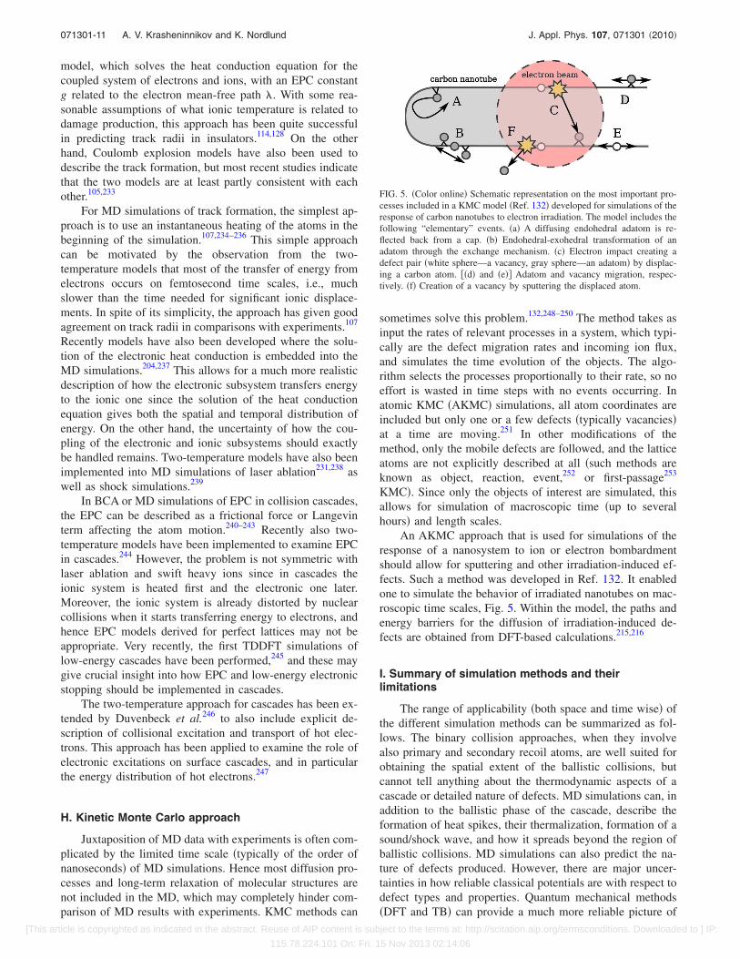
An AKMC approach that is used for simulations of theresponse of a nanosystem to ion or electron bombardmentshould allow for sputtering and other irradiation-induced ef-fects. Such a method was developed in Ref. 132. It enabledone to simulate the behavior of irradiated nanotubes on mac-roscopic time scales, Fig. 5. Within the model, the paths andenergy barriers for the diffusion of irradiation-induced de-fects are obtained from DFT-based calculations.215,216
I. Summary of simulation methods and theirlimitations
The range of applicability �both space and time wise� ofthe different simulation methods can be summarized as fol-lows. The binary collision approaches, when they involvealso primary and secondary recoil atoms, are well suited forobtaining the spatial extent of the ballistic collisions, butcannot tell anything about the thermodynamic aspects of acascade or detailed nature of defects. MD simulations can, inaddition to the ballistic phase of the cascade, describe theformation of heat spikes, their thermalization, formation of asound/shock wave, and how it spreads beyond the region ofballistic collisions. MD simulations can also predict the na-ture of defects produced. However, there are major uncer-tainties in how reliable classical potentials are with respect todefect types and properties. Quantum mechanical methods�DFT and TB� can provide a much more reliable picture of
FIG. 5. �Color online� Schematic representation on the most important pro-cesses included in a KMC model �Ref. 132� developed for simulations of theresponse of carbon nanotubes to electron irradiation. The model includes thefollowing “elementary” events. �a� A diffusing endohedral adatom is re-flected back from a cap. �b� Endohedral-exohedral transformation of anadatom through the exchange mechanism. �c� Electron impact creating adefect pair �white sphere—a vacancy, gray sphere—an adatom� by displac-ing a carbon atom. ��d� and �e�� Adatom and vacancy migration, respec-tively. �f� Creation of a vacancy by sputtering the displaced atom.
071301-11 A. V. Krasheninnikov and K. Nordlund J. Appl. Phys. 107, 071301 �2010�
[This article is copyrighted as indicated in the abstract. Reuse of AIP content is subject to the terms at: http://scitation.aip.org/termsconditions. Downloaded to ] IP:
115.78.224.101 On: Fri, 15 Nov 2013 02:14:06

defect properties, but are quite limited in the number of at-oms and time scale they can handle. There is an additionalcomplication related to small atom-atom separations duringthe development of a cascade. If pseudopotential or similarmethods such as the projected augmented wave254 techniqueare used, the separation between the atoms can be smallerthan the core radii, which limits the maximum energy of theimpinging ion. Different KMC approaches are well suited todescribe atom migration on both space and time scales ex-ceeding those in MD by orders of magnitude, but great effortis often needed to parametrize the KMC reliably.
Electronic and optical excitations can in principle befully described by TDDFT, but this approach is extremelytime consuming, and treatment of all possible excitations,transport, and recombination processes in the collisionalphase of a cascade in a dense material will remain beyondreach far into the future. Phenomenological models can beused to treat electronic and possibly also optical excitationson a case-by-case basis.
V. IRRADIATION EFFECTS IN CARBONNANOSYSTEMS
The big interest in irradiation effects in carbon nanoma-terials, such as fullerenes,255 single- and multiwallednanotubes256 �SWNTs and MWNTs�, graphene,79 andnanodiamonds,57 stems from the high technological impor-tance of these systems due to their unique mechanical andelectronic properties which can further be tailored by irradia-tion. The rich physics and intriguing behavior of nanostruc-tured carbon under irradiation comes from the unique abilityof carbon atomic networks to reorganize their structures likeno other material can do. New bonds around defects restruc-ture the lattice by creating a modified but coherent network,which can retain many of its original properties. In additionto sp2-hybridized structures including graphene and nano-tubes, carbon also exists in sp3 �diamond� and sp1 �linearcarbene chains� forms,257,258 as well as in hybridstructures.259 The difference in cohesive energies corre-sponding to different phases of carbon systems is very small.By using energetic particle beams one can drive the systemaway from equilibrium due to beam heating effects, defectcreation and annealing and different responses of differentphases due to irradiation. Then, under certain conditions, onecan quench it into a metastable atomic configuration. Forexample, irradiation can give rise to transformations ofgraphite to diamond at the nanoscale,6 cause BN fullerenegrowth,260,261 or stimulate the formation of carbon nanotubesby injecting sputtered carbon atoms into metalparticles.262,263
As in bulk solids, irradiation effects in nanoscale mate-rials cannot be fully understood without the precise knowl-edge of how defects are formed. The damage production insp2-bonded carbon nanomaterials is somewhat different fromthat observed in most other solids. For example, due to theopen structure of the nanotubes �isolated or bundled up�,even recoils that have received energy only slightly abovethe threshold energy can be displaced quite far, which is incontrast to many other types of materials �e.g., in denselypacked metals a stable interstitial-vacancy pair is normally
formed by a replacement collision sequence264�. Likewise,every displacement of a carbon atom from a suspendedgraphene sheet should give rise to formation of a defect �un-less the displaced atom remains attached to the graphenesheet�. There are many other peculiarities in defect produc-tion, as detailed below.
Because nanotubes, graphene, and graphite are excellentheat and charge conductors, the irradiation-induced changesin these sp2-bonded carbon systems are governed byknock-on atom displacements72 under electron or ion beams.This appears to be true for both metallic and narrow-bandsemiconducting carbon systems, e.g., nanotubes, as the gapin the latter is quite small, around 1 eV.256
A. Defect production in carbon nanosystems underirradiation
As mentioned in Sec. I, the experimental techniquesused to detect and characterize irradiation-induced defects inmaterials cannot give any information on the defect creationprocess, as it occurs on the picosecond time scale, but atom-istic computer simulations have provided lots of insight intoirradiation damage creation. In this section, we dwell on de-fect production in various carbon nanomaterials as revealedby calculations and corroborated by many experiments.
1. Production of defects in SWNTs under ionirradiation
Computer simulations30,174,176,265–274 of electron and ionirradiation of nanotubes proved to be a very useful tool forunderstanding the defect production mechanisms, relativeabundance of particular types of defects, and defect atomicstructures. The simulations showed that if the energy of theimpinging particle �electron or ion� is high enough, the col-lision of the particle with a carbon atom in a SWNT willresult in displacement of the atom, i.e., formation of a va-cancy �single vacancy �SV� or multivacancies, see Figs. 6and 16� and a number of primary recoil atoms which leavethe tube. Energetic recoils can displace other atoms from theSWNT. The displaced C atoms frequently adsorb onto thetube walls, Figs. 6�a� and 6�b�. These adsorbed atoms �ada-toms� play the role of interstitials174,175 in nanotube samples.
SV
A
A(a) (b)
(c)
FIG. 6. �Color online� Molecular models of carbon nanotubes with pointdefects. �a� Short fragment of a SWNT with a SV and double-coordinatedcarbon atoms �a� adsorbed onto the outer and inner surfaces of the tube. �b�Carbon adatoms in different configurations on a zigzag nanotube. �c� SWtopological defect associated with the rotation of a C–C bond. Thin linescorrespond to the atomic network of the pristine tube.
071301-12 A. V. Krasheninnikov and K. Nordlund J. Appl. Phys. 107, 071301 �2010�
[This article is copyrighted as indicated in the abstract. Reuse of AIP content is subject to the terms at: http://scitation.aip.org/termsconditions. Downloaded to ] IP:
115.78.224.101 On: Fri, 15 Nov 2013 02:14:06

Notice that due to the quasi-1D morphology, all displacedatoms can be sputtered from the SWNT, so that no interstitialcan exist in the system �placing an atom in the center of ahexagon would be geometrically easy, but is chemically ex-tremely unfavorable�. Due to voids in the SWNT, theinterstitial-vacancy �Frenkel pair� separation can be large,preventing instant recombination even at modest energies ofincident particles.
An illustration of the production of defects in single-walled carbon nanotubes deposited on a Pt substrate is pre-sented in Fig. 7. The initial motion direction of the impingingAr ion �circled� is designated by the arrow. The light spheresrepresent Pt atoms and the darker ones C atoms. The firstsnapshot �a� shows the original atom configuration in thenanotube-Pt substrate system. The Ar ion creates vacanciesin the uppermost part of the nanotube wall as well as primaryC recoils, Fig. 7�b�. Some other C atoms are sputtered fromthe nanotube. The Ar ion hits the substrate and gives rise tothe development of a collision cascade, Fig. 7�c�. The Ar ionis reflected back from the surface creating some extra dam-age in the nanotube, Fig. 7�d�. A pressure wave has devel-oped in the nanotube Fig. 7�e�. The final configuration aftercooling down the system to the zero temperature is shown inFig. 7�f�.
As for ion irradiation of isolated nanotubes, impacts of50–3000 eV Ar ions onto SWNTs were modeled in Refs. 174and 175 by the EP MD method. The SWNTs were assumedto be suspended by their ends �such nanotubes can be experi-mentally manufactured275�. It was found that SVs were themost prolific defects in nanotubes that appeared after ionimpacts. Carbon adatoms on both external and internal sidesof the nanotube walls were also common. Besides this, othercomplex defects such as SW defects and amorphous regionswere observed.
The average number of defects in a freestanding �sus-pended� �8,8� SWNT per ion impact is presented in Fig. 8.The total number of defects increases with ion energy andreaches its maximum at an ion energy of about 0.7 keV. Thereason for such behavior is that at low energies the damageproduction grows with ion energy since there is simply moreenergy available for it. At higher energies the number of SVsincreases slightly �up to �2 keV� while the number of diva-cancies �DVs� drops. The number of other defects is maxi-mal at 1.0 keV and slowly decreases at higher energies. Sucha behavior originates from a drop in the cross section fordefect production at high ion energies.175,178,276 The numberof multivacancies is less than 10% for all ion energies. Mul-tivacancies normally appear when the ion tangentially hitsthe sides of the tubes. The abundance of SVs and multiva-cancies does not correlate with their relative stability277–280 atroom and lower temperatures, but at temperatures above300 °C multivacancy abundance may be affected by theirenergetics due to defect coalescence. At high ion energies, afurther drop in the number of defects is expected. This isfundamentally different from the production of defects underion irradiation in bulk materials, where the total number ofdefects always grows with ion energy, but the peak in thedefect density is moved farther away from the surface.
The number of defects produced by the ion is larger insupported nanotubes �lying on a substrate� due to backscat-tered ions and atoms sputtered from the substrate, Fig. 9.Here the total damage is characterized by the number of Catoms with a coordination other than three �recall that allcarbon atoms in the intact nanotube are three coordinated�. Itis also evident that high-temperature annealing decreases thenumber of defects 20%–50% due to recombination of Fren-kel pairs. The residual damage after annealing was found tobe practically independent of the substrate type.175
Qualitatively similar results were obtained for othertypes of ions178,265 with energies up to 1 keV. It is interestingto notice that in this interval of energies Xe and Kr ionscreate approximately the same amount of damage �despitethe difference in ion masses�. This behavior can be under-stood in terms of the cross section for the defect productionin a SWNT. The cross sections for different ions wereestimated178,265 by calculating the maximum impact param-eter for which the ion transfers at least 25 eV to a C atom ina binary collision �25 eV is slightly above the experimental
a) b)
e)
f)
c) d)
FIG. 7. Illustration of the production of defects in carbon nanotubes depos-ited on Pt substrates. The initial movement direction of the impinging Ar ion�circled� is designated by the arrow. The light spheres represent Pt atomsand the darker ones C atoms. The first snapshot �a� shows the original atomconfiguration in the nanotube-Pt substrate system. The Ar ion creates vacan-cies in the uppermost part of the nanotube wall as well as primary C recoils�b�. Some other C atoms are sputtered from the nanotube. The Ar ion hits thesubstrate and gives rise to the development of a collision cascade �c�. The Arion is reflected back from the surface creating some extra damage in thenanotube �d�. A pressure wave has developed in the nanotube �e�. The finalconfiguration after cooling down the system to the zero temperature �f�.From Ref. 175.
0.05 0.1 0.2 0.5 1.0 2.0 10.0
Ion energy [keV]
0.0
0.2
0.4
0.6
0.8
1.0
1.2
Num
ber
ofde
fect
s OtherAdatomsDVSV
FIG. 8. �Color online� Average numbers of SVs, DVs, adatoms, and otherdefects per Ar ion impact as functions of ion energy in a �8,8� SWNT. Thesymbols are simulation results, lines are guides to the eye, from Ref. 276.
071301-13 A. V. Krasheninnikov and K. Nordlund J. Appl. Phys. 107, 071301 �2010�
[This article is copyrighted as indicated in the abstract. Reuse of AIP content is subject to the terms at: http://scitation.aip.org/termsconditions. Downloaded to ] IP:
115.78.224.101 On: Fri, 15 Nov 2013 02:14:06

value of the threshold energy for displacing an atom in thenanotube, see Sec. V A 5, but this is the threshold energy fordisplacing a C atom in the EP Brenner model used in the MDsimulations� The cross sections S �S=p2 where p is theimpact parameter� for various ions are presented in Fig. 10. Itis evident that the averaged cross sections for Kr and Xe ionsare roughly the same. This is why the damage created bythese ions is approximately equal in the energy range con-sidered.
2. Production of defects in multiwalled and bundled-up nanotubes
In addition to the simple point defects discussed above,MD simulations178,271,272,281,282 showed that a number ofmore complex defects can be formed in MWNTs andbundles of SWNTs. Important examples of these defects areintershell covalent bonds �formed, e.g., by two danglingbonds at the vacancies in the adjacent shells� in MWNTs, seeFig. 11�a�. Likewise, defect-mediated covalent bonds be-tween adjacent SWNTs in the bundle can appear, Fig. 11�b�.
In Ref. 282, the formation of cross-links between neigh-boring carbon nanotubes within a bundle under self-irradiation �irradiation with C ions� was studied by classical
MD. It was shown that it is possible to polymerize carbonnanotubes through irradiation. Cross-links were found to becreated mainly in the direction perpendicular to the surface,and for higher energies, defects are created deeper in therope. Qualitatively similar results were reported for Ar ion283
and CH3 �Ref. 272� radical irradiation. High irradiating doseseventually amorphize the tubes, Fig. 11�c�.
3. Ion irradiation of fullerenes and fullerene-nanotubesystems
The interest in ion irradiation of fullerenes was stimu-lated by reports on formation of diamond nanocrystals �NCs�inside carbon onions �multishell fullerenes� under Ne ionirradiation.284
Besides this, ordering of fullerene thin films under high-energy ion irradiation �200 MeV Au and 60 MeV Ni ions�has been reported,66 probably due to effects of ion-beamheating and a vanishingly small probability for defect pro-duction in a very thin target. Besides this, fullerene filmsirradiated with 250 keV Ar and 92 MeV Si ions showedmagnetic response,285 as evidenced by magnetic measure-ments using a superconducting quantum interference deviceand magnetic force microscopy. A ferromagnetic behaviorincreasing with ion fluence was observed. The magnetizationwas attributed to the formation of an amorphous carbon net-work and to the incorporation of oxygen in the irradiatedfilms. Low-dose irradiation also gave rise to another interest-ing phenomenon: conducting NWs parallel to each other,embedded in fullerene matrix were synthesized by high en-ergy heavy ion bombardment of thin fullerene films.106 Thetypical diameter of the conducting tracks was about 40–100nm. The creation of conducting wires could be explained bytransformation of fullerene to conducting forms of carbon inthe ion track, surrounded by the polymerized zone.
Theoretically, the interaction of Ar ions withC60@C240@C540 carbon onions were studied by EP MD.286
It was shown that the pentagons in the graphitic network andtheir nearest environment are the least stable regions in thecarbon onion under irradiation. The energy threshold for theformation of a vacancy in a pentagon of the onion fullereneshell was examined in two temperature regimes �300 and1000 K�, and it was found that the threshold for defect for-mation decreases with temperature. The simulation resultsprovided direct confirmation of the possibility of formation
0 0.5 1 1.5 2Incident ion energy (keV)
0
5
10
15
20
25
Defectnumbers
Pt substrateSuspendedPt substrate, annealedSuspended, annealed
FIG. 9. Average coordination defect numbers for irradiated SWNTs as func-tions of incident Ar ion energy. Full circles/squares stand for the number ofC atoms with a coordination other than three for suspended/supported nano-tubes. Open circles/squares are the corresponding coordination defect num-bers after 100 ps annealing at 1500 K.
FIG. 10. Cross section for the defect production in nanotubes as a functionof incident ion energy for various ions.
(b)
(c)
(a)
FIG. 11. �Color online� Irradiation induced links between nanotubes. �a� Acovalent bond between two nearby vacancies in the adjacent shells of aMWNT. �b� Covalent bonds between SWNTs in a nanotube bundle. �c� Theatomic network of a MWNT before and after 300 eV Ar ion irradiation witha dose of 2�1016 cm−2 as simulated with EP MD.
071301-14 A. V. Krasheninnikov and K. Nordlund J. Appl. Phys. 107, 071301 �2010�
[This article is copyrighted as indicated in the abstract. Reuse of AIP content is subject to the terms at: http://scitation.aip.org/termsconditions. Downloaded to ] IP:
115.78.224.101 On: Fri, 15 Nov 2013 02:14:06

of a diamond structure upon ion irradiation of carbon onions.Additional information on the mechanism of diamond nucle-ation in the fullerene cores was obtained from DFT-based TBsimulations287 of irradiation of a prototype icosahedral two-shell fullerene C60@C240. It was possible to identify regionsin which almost all carbon atoms become sp3-bonded. Addi-tionally, a counteracting tendency for the carbon atoms toform shell-like substructures was observed. Thus it wasshown that, to shift the balance between these two processestoward diamond nucleation, strongly nonequilibrium condi-tions are required.
MD simulations273 were also used to study ionirradiation-induced transformations in other hybrid systems,such as carbon nanopeapods �fullerenes encapsulated insidecarbon nanotubes�. The results confirmed the effectiveness ofion bombardment in inducing chemical modifications ofnanopeapods. The simulations showed that the coalescenceof C60 molecules starts with the damage of fullerenes andintermolecular bridging. The cross-linking of C60 moleculesto the tube wall was also predicted. This cross-linking resultsin changes in the electronic band structure as compared tothe unmodified nanopeapod, which was investigated usingDFT methods. Further information on the type of irradiation-induced bonds and their effects on the local electronic struc-ture was obtained from hybrid Hartree–Fock/DFTcalculations.288
4. Simulations of electron irradiation of carbonnanosystems
As discussed in Sec. II, the electron-atom collision timeis extremely short �10−21 s, Ref. 72�, so that the impacts ofenergetic electrons onto carbon nanosystems can bemodeled43,46,210,212,271,289 by assigning some kinetic energy toa carbon atom in the atomic network and then by using theMD method to simulate the subsequent atom motion to un-derstand if the impact gave rise to the formation of a defect.The orientation of the initial velocity vector can be choseneither randomly if the main goal is to simulate the responseof the system to a prolonged irradiation or in the direction,43
which will more likely result in the formation of a defect, ifthe defect formation energy is the quantity of interest. Thetypical simulation setup with the initial velocity vector beingperpendicular to the tube surface and several snapshotsshowing the atom positions after electron impact onto a zig-zag nanotube are presented in Fig. 12. The initial energy ofthe recoil atom was chosen just above the threshold for de-fect production.
Such a setup has been successfully used to calculate thedisplacement energies of atoms from graphene and carbonnanotubes,46,210,212 as well as from SiC nanotubes,213 seeSec. V A 5. However, for simulations of high dose irradia-tion, the MD simulations for atoms should be combined withan algorithm that could make it possible to generate a real-istic distribution of initial velocities of recoil atoms.
Such an attempt was recently made290 by augmentingMD with a Monte Carlo method using the elastic-scatteringcross section, which described the interaction between a highenergy incident electron and the recoil carbon atom. Themodel was applied to carbon nanotubes and provided reason-able agreement with the experiments. The advantage of themodel is that it made it possible to correlate the response ofnanotubes to irradiation with incident electron energy, tubediameter, and tube temperature. The drawback of the ap-proach is an unrealistically high current density �ten ordersof magnitude higher than in experiments� required in simu-lations due to computational limitations on the time intervalbetween consecutive impacts of electrons into the system�otherwise the simulation time would have been prohibi-tively long�. Besides, the EP MD with the Brenner modelwas used, which is inferior to TB model due to a loweraccuracy and inadequate description of bond breaking due toartificial cutoff functions.291
5. Carbon atom displacement energy
The displacement threshold energy Td is an importantcharacteristic describing the radiation hardness of a material.Td can be defined as the minimum kinetic energy that mustbe delivered to an atom due to the impact of an energeticparticle, in order for the atom to leave its position in theatomic network and either take a metastable �interstitial� po-sition in the lattice or leave the system. Td is different fordifferent carbon allotropes,72,292 as it is related to not only thebond energy but also the local chemical bonding and theavailability of open space in the structure. Td is smaller insp2-bonded carbon �15–20 eV� than in diamondlike struc-tures �30–48 eV�.
Moreover, Td may depend on the system geometry, forexample, on the diameter of a nanotube, that is, on the cur-vature of the atomic network, or on nanotube chirality. Earlyexperimental and theoretical studies42,43 revealed a stronglyanisotropic threshold for atomic displacement, but did notreport any dependence on the chirality. It was shown that inan isolated SWNT with a diameter over 1 nm, a lower energy�roughly half the value� is required to displace a carbon atominto the direction perpendicular to the tube surface �Td
�15–17 eV�, than into the tangential direction �30–50 eV�.This value �perpendicular direction� was very close to thecorresponding value for graphite �15–20 eV�.72
Later calculations46,210 showed that for small nanotubeswith diameters less than 1 nm, Td indeed depends on the tubediameter and chirality. Figure 13 shows Td as a function oftube diameter for armchair nanotubes. The energy was cal-culated by a DFTB-based TB model dynamically �diamonds�and statically �triangles�. In the dynamical approach, somekinetic energy was assigned to a carbon atom in the nanotubenetwork, then the MD method was used to simulate the be-
0fs5fs 9fs 50fs
68fs 120fs 150fs
FIG. 12. �Color online� The setup used in simulations of electron irradiationof carbon nanotubes �side view� and several snapshots showing the atompositions after electron impact onto a zigzag nanotube. The initial energy ofthe recoil atom is just above the threshold for defect production.
071301-15 A. V. Krasheninnikov and K. Nordlund J. Appl. Phys. 107, 071301 �2010�
[This article is copyrighted as indicated in the abstract. Reuse of AIP content is subject to the terms at: http://scitation.aip.org/termsconditions. Downloaded to ] IP:
115.78.224.101 On: Fri, 15 Nov 2013 02:14:06
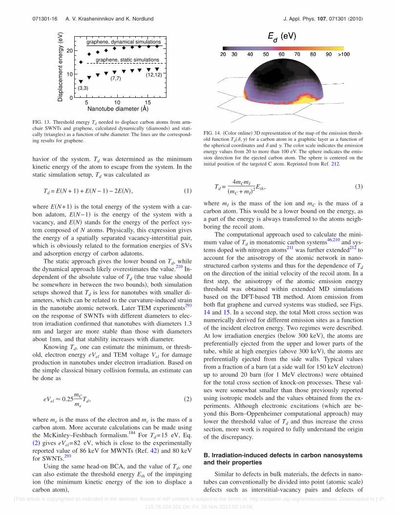
havior of the system. Td was determined as the minimumkinetic energy of the atom to escape from the system. In thestatic simulation setup, Td was calculated as
Td = E�N + 1� + E�N − 1� − 2E�N� , �1�
where E�N+1� is the total energy of the system with a car-bon adatom, E�N−1� is the energy of the system with avacancy, and E�N� stands for the energy of the perfect sys-tem composed of N atoms. Physically, this expression givesthe energy of a spatially separated vacancy-interstitial pair,which is obviously related to the formation energies of SVsand adsorption energy of carbon adatoms.
The static approach gives the lower bound on Td, whilethe dynamical approach likely overestimates the value.210 In-dependent of the absolute value of Td �the true value shouldbe somewhere in between the two bounds�, both simulationsetups showed that Td is less for nanotubes with smaller di-ameters, which can be related to the curvature-induced strainin the nanotube atomic network. Later TEM experiments293
on the response of SWNTs with different diameters to elec-tron irradiation confirmed that nanotubes with diameters 1.3nm and larger are more stable than those with diametersabout 1nm, and that stability increases with diameter.
Knowing Td, one can estimate the minimum, or thresh-old, electron energy eVel and TEM voltage Vel for damageproduction in nanotubes under electron irradiation. Based onthe simple classical binary collision formula, an estimate canbe done as
eVel � 0.25mC
meTd, �2�
where me is the mass of the electron and mc is the mass of acarbon atom. More accurate calculations can be made usingthe McKinley–Feshbach formalism.184 For Td=15 eV, Eq.�2� gives eVel=82 eV, which is close to the experimentallyreported value of 86 keV for MWNTs �Ref. 42� and 80 keVfor SWNTs.293
Using the same head-on BCA, and the value of Td, onecan also estimate the threshold energy Eth of the impingingion �the minimum kinetic energy of the ion to displace acarbon atom�,
Td =4mCmI
�mC + mI�2Eth, �3�
where mI is the mass of the ion and mC is the mass of acarbon atom. This would be a lower bound on the energy, asa part of the energy is always transferred to the atoms neigh-boring the recoil atom.
The computational approach used to calculate the mini-mum value of Td in monatomic carbon systems46,210 and sys-tems doped with nitrogen atoms211 was further extended212 toaccount for the anisotropy of the atomic network in nano-structured carbon systems and thus for the dependence of Td
on the direction of the initial velocity of the recoil atom. In afirst step, the anisotropy of the atomic emission energythreshold was obtained within extended MD simulationsbased on the DFT-based TB method. Atom emission fromboth flat graphene and curved systems was studied, see Figs.14 and 15. In a second step, the total Mott cross section wasnumerically derived for different emission sites as a functionof the incident electron energy. Two regimes were described.At low irradiation energies �below 300 keV�, the atoms arepreferentially ejected from the upper and lower parts of thetube, while at high energies �above 300 keV�, the atoms arepreferentially ejected from the side walls. Typical valuesfrom a fraction of a barn �at a side wall for 150 keV electron�up to around 20 barn �for 1 MeV electrons� were obtainedfor the total cross section of knock-on processes. These val-ues were somewhat smaller than those previously reportedusing isotropic models and the values obtained from the ex-periments. Although electronic excitations �which are be-yond this Born–Oppenheimer computational approach� maylower the threshold value of Td and thus increase the crosssection, more work is required to fully understand the originof the discrepancy.
B. Irradiation-induced defects in carbon nanosystemsand their properties
Similar to defects in bulk materials, the defects in nano-tubes can conventionally be divided into point �atomic scale�defects such as interstitial-vacancy pairs and defects of
FIG. 13. Threshold energy Td needed to displace carbon atoms from arm-chair SWNTs and graphene, calculated dynamically �diamonds� and stati-cally �triangles� as a function of tube diameter. The lines are the correspond-ing results for graphene.
FIG. 14. �Color online� 3D representation of the map of the emission thresh-old function Td�� ,� for a carbon atom in a graphitic layer as a function ofthe spherical coordinates and � and . The color scale indicates the emissionenergy values from 20 to more than 100 eV. The sphere indicates the emis-sion direction for the ejected carbon atom. The sphere is centered on theinitial position of the targeted C atom. Reprinted from Ref. 212.
071301-16 A. V. Krasheninnikov and K. Nordlund J. Appl. Phys. 107, 071301 �2010�
[This article is copyrighted as indicated in the abstract. Reuse of AIP content is subject to the terms at: http://scitation.aip.org/termsconditions. Downloaded to ] IP:
115.78.224.101 On: Fri, 15 Nov 2013 02:14:06

higher dimensions, for example, a local change in the chiral-ity can be interpreted as a dislocation.7 Dislocations shouldbe particularly abundant in mechanically strainednanotubes.294 Dislocation lines have also been observed ingraphene.295 As mentioned above, the most prolific point de-fects, which appear under both electron and ion irradiation incarbon nanosystems, are SVs and multivacancies, adatoms,and interstitials. In this section, we briefly discuss the atomicstructure and properties of the defects.
1. Vacancies in graphene and carbon nanotubes
Unlike metals,296 where the structure of a vacancy isessentially a missing atom in the lattice, carbon nanotubesexhibit a strong reconstruction of the atomic network nearthe vacancy, which, as discussed below, results in many in-teresting effects, e.g., pressure buildup inside irradiatednanotubes.19,297
DFT and DFT-based TB calculations216,298–302 showedthat SVs in nanotubes reconstruct by saturating two danglingbonds and forming a pentagon, see Fig. 16. In graphite, SVsreconstruct as well due to the Jahn–Teller distortion.303–305
However, in nanotubes, the reconstruction is much strongerdue to the curvature and inherent nanosize of the system. It iseasier for the tube to contract locally to “heal” the hole andthus saturate energetically unfavorable dangling bonds. Thecurvature gives rise to a shorter bond in the pentagon �ascompared to the bond in graphite� and a considerable drop inthe vacancy formation energy Esv, Fig. 17 �Esv�7.5 eV in
FIG. 15. �Color online� �a� Schematic representation of the irradiation ge-ometry for a carbon nanotube, radius R, projected onto the XZ plane. Thenanotube has its axis along Y perpendicular to the incident electron beam.�b� Total knock-on cross section for carbon atoms in a single-walled carbonnanotube as a function of their position around the tube circumference.Angles �=0° and �=90° refer, respectively, to carbon atoms in the tubebase and in the tube side. The electron beam is entering vertically from thetop of the figure. Total cross section for the full tube �0° ���90°� can beobtained by symmetrization of the plot. The curves are plotted for incidentelectron energies between 130 keV and 1 MeV representative of the voltagesused in TEM. Reprinted from Ref. 212.
DV
SVA
5
5
5
57
7
8
5
5
7 7
tetra Vac
topview
sideview
(b) (c)(a)
SV
reconstruction reconstruction
reconst-ruction
reconst-ruction
stable
metastable
FIG. 16. �Color online� Reconstructions of the atomic network near vacan-cies in single-walled carbon nanotubes. Only front walls of the nanotubesare shown. �a� Reconstruction of a SV in a �6,6� armchair carbon nanotube.The top panel shows the original nonreconstructed configuration which isunstable with respect to the Jahn–Teller distortion. Depending on the orien-tation of the new weak “pentagon bond,” the reconstructed configurationscan be metastable �when the bond is parallel to the tube axis� or stable�when the bond is almost perpendicular to the tube axis�. The latter configu-ration has lower energy. �b� Reconstructions of the atomic network of a�10,10� carbon nanotube with several point defects. A DV transforms to anagglomeration of five- and eight-membered rings. A SV and an adatom mayform a metastable SW �5757� defect. �c� Reconstruction of a tetravacancy.Note that the effective size of the “hole” decreases at the expense of localdiameter reduction, so that carbon nanotubes can be referred to as self-healing materials.
FIG. 17. Formation energies of SVs and DVs in armchair and zigzag nano-tubes as functions of nanotube diameter as calculated by the TB and DFTmethods �Ref. 216�.
071301-17 A. V. Krasheninnikov and K. Nordlund J. Appl. Phys. 107, 071301 �2010�
[This article is copyrighted as indicated in the abstract. Reuse of AIP content is subject to the terms at: http://scitation.aip.org/termsconditions. Downloaded to ] IP:
115.78.224.101 On: Fri, 15 Nov 2013 02:14:06

graphite305,306�. Here Esv is calculated as usual through theformula
Esv = E�N − 1� + E�N�/N − E�N� , �4�
where E�N� is the total energy of the system composed of Ncarbon atoms. Esv is positive and physically defines the en-ergy required to remove an atom from the system and placeit into a vacant position at the surface far away from theoriginal position of the atom.
As curvature breaks the trigonal symmetry of thegraphene sheet, the configuration when the new bond in thepentagon is parallel �or nearly parallel� to the tube axis ishigher in energy as compared to the case when the bond isperpendicular to the axis, Fig. 16�a�. Similar phenomena oc-cur in nanotubes with other chiralities, and Esv is affected bythe orientation of the new bond.
DVs in nanotubes also reconstruct, see Fig. 16�b�. Onecan expect the DV formation energy Edv in nanotubes to besmaller than the formation energy of two SVs, as there are nodangling bonds in the system. The DV formation energyEdv=8.7 eV in graphite305 is indeed lower than twice Esv=7.7 eV. Edv was calculated216 for armchair and zigzagnanotubes as a function of nanotube diameters �see Fig. 17�.Similar to Esv for SVs, Edv decreases when the diameterbecomes smaller, which can be understood in terms of theeasier reconstructions of the nanotube atomic network. Thediameter locally decreases, so no dangling bond or stronglystrained bonds �typical for the case of graphite� are present.However, most surprising is that for nanotubes Edv is smallerthan the formation energy of one SV. Such behavior is inher-ently related to the nano size and the unique atomic structureof SWNTs and is fundamentally different from that of mostmonoatomic solids,307 including graphite.305 Extrapolatingthe data presented in Fig. 17, one can assume that this is thecase for nanotubes with diameters under 30 Å or even larger.It is important that, unlike DVs, SVs always have a danglingbond, so that a perfect reconstruction around a SV is notpossible.
Saturation of dangling bonds and the local contraction ofthe nanotube also take place for multivacancies.277 Thus car-bon nanotubes can be referred to as self-healing materialsunder irradiation. An additional piece of evidence for self-healing of irradiation-induced defects in nanotubes was re-cently obtained in experiments on controlled telescopic mo-tion of MWNTs in a TEM.308 Defects with dangling bondsintentionally introduced in the MWNTs by electron irradia-tion led to temporary mechanical dissipation, but self-healingrapidly optimized the atomic structure and restored smoothmotion.
Further reconstructions of nanotube atomic network canoccur by rotations of carbon-carbon bonds near vacancies.For example, a DV, which can be referred to as a 585 defect�two pentagons and one octagon�, see Fig. 18, can be trans-formed to a 555 777 defect, which is energetically more fa-vorable in nanotubes with large �about 5 nm� diameters,309
graphene,310 and graphene ribbons.311
The advent of high-resolution TEMs equipped with ab-erration correctors made it possible to achieve a resolution ofbetter than 1 Å and directly see individual point defects in
carbon systems, especially in graphene membranes.295,312
Figure 19 shows defects found in TEM image sequences, andamong them, Figs. 19�e�–19�g�, a reconstructed vacancy: �e�original image and �f� showing atomic configuration; a pen-tagon is indicated in green. The unperturbed lattice was im-aged after 4 s �g�, possibly due to recombination of the va-cancy with a carbon adatom. Note that electron beam energywas 80 keV, close to the threshold value to displace a carbonatom from a graphene sheet, Sec. V A 5, so that the observeddefects were likely created by the electron beam.
Isolated SVs and DVs and defect constellations havealso been observed in graphene by a TEM operating at 100kV.295 It was assumed that these defects had been producedby electron bombardment. Figure 20 shows the TEM imagesand the atomic structure of he defects. The atomic networkappears to be slightly distorted, possibly due to mechanicalstress induced by nearby defects.
(a) (b) (c)
5
5
5 5
5
8 7 7
7
FIG. 18. �Color online� Formation of a 555 777 defect from a DV by bondrotation. �a� The atomic structure of a DV, which can be referred to as a 585defect �two pentagons and one octagon�. The bond to be rotated is circled.�b� 555 777 defect which is energetically more favorable in nanotubes withlarge diameters and graphene. �c� Both structures are presented in the sameimage.
FIG. 19. �Color online� Defects found in HRTEM image sequences. ��a�–�d�� SW defect: �a� unperturbed lattice before appearance of the defect, �b�SW defect �c� same image with atomic configuration superimposed, �d�relaxation to unperturbed lattice �after approximately 4 s�. ��e�–�g�� Recon-structed vacancy: �e� original image and �f� showing atomic configuration; apentagon is indicated in green. �g� Unperturbed lattice, 4 s later. ��h� and �i��Defect image and configuration consisting of four pentagons �green� andheptagons �red�. Note the two adjacent pentagons. ��j� and �k�� Defect imageand configuration consisting of three pentagons �green� and three heptagons�red�. This defect returned to the unperturbed lattice configuration after 8 s.In spite of the odd number of five to seven pairs, this is not a dislocationcore �it is compensated by the rotated hexagon near the center of the struc-ture�. All scale bars are 2 Å. From Ref. 312.
071301-18 A. V. Krasheninnikov and K. Nordlund J. Appl. Phys. 107, 071301 �2010�
[This article is copyrighted as indicated in the abstract. Reuse of AIP content is subject to the terms at: http://scitation.aip.org/termsconditions. Downloaded to ] IP:
115.78.224.101 On: Fri, 15 Nov 2013 02:14:06

2. Carbon adatoms as interstitials in single-walledcarbon nanotubes
The adsorption of carbon adatoms onto nanotubes215 wasrecently studied by DFT-based methods. It was found thatthe adatom on the outer surface of the SWNT occupies thebridge position above the C–C bond. Similar to vacancies,due to the SWNT curvature the adatom adsorption onto sitesabove C–C bonds being parallel and perpendicular to thenanotube axis results in different adsorption energies and lo-cal atom arrangements, see Fig. 6�b�. Adatoms inside theSWNT are displaced from the bridge position due tocurvature-enhanced interactions with the neighbor atoms.
In Fig. 21, the adatom adsorption energies are shown asfunctions of nanotube diameters for armchair SWNTs. Foradatoms on the outer surface, the absolute value of Ea de-creases with an increase in the SWNT diameter. This seemsto be a general tendency: similar behavior of Al, H,313 and N�Ref. 314� adatoms on SWNTs has been reported. The ad-sorption energy is always lower for configurations when theadatom is above the C–C bond oriented perpendicular to theSWNT axis than for the “parallel” configuration. This can beunderstood from simple carbon bonding considerations. Inthe “perpendicular” case, it is easier for the adatom to pullthe two adjacent nanotube atoms apart �notice that the bond
is actually broken, thus avoiding the energetically unfavor-able four-coordinated atom configurations�. Similar resultswere obtained for zigzag nanotubes.215,315
3. Carbon adatoms on graphene
Carbon adatoms316 on graphene, which have been alsoreferred to as self-interstitials, have received particular atten-tion due to their possible contribution to intrinsic magnetismin all-carbon systems316,317 and in the context of engineeringthe atomic network of sp2-bonded nanostructures.318–320
The adatoms occupy the position on top of the middle ofa C–C bond in graphene, Fig. 22�b�. Besides this, two othermetastable configurations with slightly higher energies arepossible,320,321 as shown in Fig. 22�a� and 22�c�. The ada-toms can easily migrate over the graphene surface with amigration barrier of about 0.4 eV.215,315 This means that ada-toms on flat graphene flakes are highly mobile at room andelevated temperatures and can hardly be detected with TEMor STM. At the same time, as curvature decreases adatomdiffusivity, Sec. V B 6, the interpretation of TEMobservations7 in terms of adatoms can be consistent withtheoretical results, if the graphene surface is slightly curved.The dumbbell configuration is important in the context ofmigration of carbon interstitials in graphite and onions in thedirection perpendicular to carbon layers, as discussed in Sec.V B 6.
When two adatoms form a dimer, they can be incorpo-rated into the network of sp2-hybridized carbon atoms at theexpense of local curvature of the network,318 Figures 23�a�and 23�b�. Such defects which look like two pentagons andtwo heptagons were named as “inverse Stone–Wales �ISW�defects.” Their formation energy is about 6 eV, even higherthan that of Stone–Wales �SW� defects so the concentrationof such defects in as-grown carbon nanostructures should bevery small. However, such defects can appear under irradia-tion if two atoms displaced from their positions and adsorbedon a graphenic structure form a dimer. Such defects are im-mobile under ambient conditions, and their agglomerationmay locally change the curvature of graphene flakes andeven give rise to blisters,318 Figs. 23�c�–23�f�.
4. Stone-Wales defects
Along with vacancy- and interstitial-type defects �atomsare missing or extra atoms are present�, defects of anothertype may exist in sp2-hybridized carbon materials: thepentagon/heptagon SW defects322 associated with a rotationof a bond in the nanotube atomic network, Fig. 6�c�. Note
FIG. 20. �Color online� High resolution TEM images of defects in graphenelattice. �a� SV and �b� DV. The images were obtained with a filter applied tothe FFT of the raw images as indicated by the inset. From Ref. 295.
FIG. 21. Adsorption energies of carbon adatoms on armchair SWNTs asfunctions of tube diameter as calculated with a TB method. The numbersstand for the tube chirality indices.
FIG. 22. Single adatoms on graphene and their relative energies: �a� dumb-bell configuration, �b� bridge position with an adatom above the midpoint ofa graphene C–C bond, and �c� an adatom displaced �off-top� from a topposition. The positions of adatoms are indicated with arrows, from Ref. 320.
071301-19 A. V. Krasheninnikov and K. Nordlund J. Appl. Phys. 107, 071301 �2010�
[This article is copyrighted as indicated in the abstract. Reuse of AIP content is subject to the terms at: http://scitation.aip.org/termsconditions. Downloaded to ] IP:
115.78.224.101 On: Fri, 15 Nov 2013 02:14:06

that the number of atoms is the same as in the pristine net-work, and that all atoms are three coordinated, so we have anexample of topological disorder. Note also that in a SW de-fect the two heptagons have a common C–C bond, while thepentagons have a common bond in an ISW defect. An ex-perimental TEM image312 of a SW defect is shown in Fig.19�b� and 19�c�.
SW defects can appear in carbon nanotubes and othersp2-bonded covalent nanostructures, e.g., SiC nanotubes,323
after impacts of energetic ions175 and electrons.46,210 SW de-fects can be produced directly by the impact of an energeticparticle or by partial recombination of an adatom and a va-cancy, as shown in Fig. 16�b�, which may explain experi-mental observations,324 of SW defect migration under theelectron beam.
SW defects are also thought to be responsible for therelease of excessive strain under axial mechanical load ofnanotubes.325–327 The formation energy of SW defectsproved to be dependent on the tube diameter andchirality,328–330 analogously to other point defects. Overall,MD simulations showed that the concentration of SW defectsafter impact of energetic ions174,175,178,265 and electrons210 ismuch smaller than those for adatoms and interstitials.
With regard to the atomic structure of SW defects ingraphene, very recent DFT and quantum Monte Carlosimulations331 showed that the structure of the defects maybe more complex than reported in the original paper.322 Itwas demonstrated that rather than being a simple in-planetransformation of two carbon atoms, out-of-plane wavelikedefect structures that extend over several nanometers mayexist with the formation energy being lower by 0.2 eV thanthat for the flat structure. Thus irradiation-induced SW de-fects may enhance the tendency of graphitic layers to roll upinto nanotubes and fullerenes and may also play a role in theintrinsic rumpling of graphene.
5. Irradiation-induced defects in MWNTs andnanotube bundles
As discussed in Sec. V A, in addition to simple pointdefects, a number of more complex defects can be formed in
MWNTs and bundles of SWNTs. Important examples ofthese defects are intershell covalent bonds �formed, e.g., bytwo dangling bonds at the vacancies in the adjacent shells� inMWNTs, see Fig. 11�a�. Likewise, defect-mediated covalentbonds between adjacent SWNTs in the bundle can appear,Fig. 11�b�. The bonds can be due to vacancies or the so-called Wigner defects,332 a metastable atom configurationformed by a vacancy and a nearby interstitial. Such struc-tures were experimentally found in TEM images of irradiateddouble-walled nanotubes �DWNTs�,39 Fig. 24. The behaviorof these complex irradiation-induced defects is governed inpart by annealing and diffusion of original defects—vacancies and interstitials. As shown below, these defectshave a profound effect on the mechanical properties of thenanotubes.
The presence of nearby walls changes the behavior ofvacancies. The focused electron beam in a TEM was recentlyused to create individual vacancies in predefined positions ofsingle- and double-walled carbon nanotubes.333 Individualvacancies in SWNTs were reported to be unstable and causean immediate reconstruction of the lattice between 20 and700 °C likely due to vacancy migration and coalescence.Note that in the geometry of the experiment, vacancies couldhave been generated in both upper and lower parts of thenanotube directly above each other. In double-walled tubes,vacancies were stable and observable up to at least 235 °C,whereas above 480 °C a relaxation of the lattice occurred,which may be associated with intershell links between thevacancies in the neighbor shells and thus lower mobility ofthe vacancies.
6. Annealing of irradiation-induced defects
Experiments on electron72 and ion334 irradiation of bothSWNTs and MWNTs indicate that much of irradiation-
FIG. 23. �Color online� SW defects and their agglomerations. ��a� and �b��Single inverse SW defect. ��c�–�f�� Multiple defects, which can be aligned toform ridged contours which can be straight, curved, or even closed, fromRef. 318.
FIG. 24. �Color online� Sequential TEM images of the interlayer defectswhich appear and disappear in DWNTs recorded at 573 K. In the ��a�–�d��side wall, several bridges connecting two graphene layers frequently appearin dark contrast �marked by red arrows� and disappear just after the obser-vation. Also in the ��e�–�h�� top wall, pairs of dark and bright contrast oftenappear and then vanish �marked by red arrows�. From Ref. 39.
071301-20 A. V. Krasheninnikov and K. Nordlund J. Appl. Phys. 107, 071301 �2010�
[This article is copyrighted as indicated in the abstract. Reuse of AIP content is subject to the terms at: http://scitation.aip.org/termsconditions. Downloaded to ] IP:
115.78.224.101 On: Fri, 15 Nov 2013 02:14:06

induced damage in nanotubes can be annealed in situ at tem-peratures higher than 300 °C, Fig. 25. Thus radiation dam-age in nanotubes can be avoided at relatively hightemperatures. Note that in most common fcc metals, closeFrenkel pairs annihilate well below room temperature �“stageI” annealing�.129
Two mechanisms govern the defect annealing.175 Thefirst mechanism is vacancy healing through dangling bondsaturation and by forming nonhexagonal rings, as describedin Sec. V B 1.
The second mechanism of annealing is the migration ofcarbon interstitials and vacancies, followed by Frenkel pairrecombination. The interstitial can migrate over the surfaceof SWNTs �isolated or bundled up�. Early calculations335,336
indicated that the adatom migration energy Em�a� is very low,
but more rigorous recent results215,316 give higher values�0.5–1 eV, the actual value depends on the tube diameter andchirality�, which is in a good agreement with experimentalvalues of Em
�a��0.8 eV.337 Recent direct observations of themigration of individual point defects in nanotubes39 andnanoscale graphite species7 are also in line with the theoret-ical results. Interstitials �adatoms� inside SWNT and hollowcores of MWNTs are highly mobile, with the migration en-ergy of 0.1–0.4 eV �depending on the diameter and chiralityof the tube�, as simulations46 indicate.
The high mobility of carbon interstitials inside SWNTshas been experimentally confirmed,46 and the migration bar-rier was measured338 to be about 0.25 eV. To do this, theirradiation dose necessary to cut nanotubes repeatedly with afocused electron beam was measured as a function of the
separation between the cuts and at different temperatures. Asthe cutting speed is related to the migration of displacedcarbon atoms trapped inside the tube and to their recombina-tion with vacancies, as sketched in Fig. 26, informationabout the mobility of the trapped atoms was obtained withina simple 1D diffusion picture. By fitting the theoretical datato the experimental curves, the migration barrier was esti-mated. The remarkably high mobility of interstitial atomsinside carbon nanotubes shows that nanotubes have potentialapplications as pipelines for the transport of carbon and otheratoms.
Migration of interstitials in the open spaces between theadjacent shells in MWNTs seems to be similar to that ingraphite. Although there are some relevant theoretical306,321
and experimental339 data for graphite, further studies are re-quired to confirm that the migration energy of interstitials inMWNTs is the same as in graphite.
Much less is known about the migration of carbon inter-stitials in graphite, MWNTs, and onions in the direction per-pendicular to carbon layers. The exchange mechanism of dif-fusion with an activation barrier of about 1.7 eV, whichincludes the dumbbell �Fig. 22�a�� as an intermediate con-figuration has been proposed.321 Earlier simulations340 gave avalue of 2.3 eV. However, experiments341 on relaxation ofstrain in carbon onions carried out in a TEM indicate that themigration barrier may be much higher, about 5 eV, in agree-ment with early data on the diffusivity of interstitials alongthe c axis in graphite.339
Recent simulations216 showed that the vacancy migrationenergy Em
�v� is above 1 eV, larger than Em�a�. Nevertheless, SVs
should be mobile already at 200 °C. The mechanism of va-cancy migration is quite complicated, and it includes twosteps: bond switching and “actual” migration of the vacancy�motion of the atom�, as illustrated in Fig. 27. Besides anni-hilating with interstitials, SVs will form DVs that are practi-cally immobile at temperatures under 1000 °C or disappearat the open ends of the tubes.
As for SW defects, the annealing should result in therestoration of the perfect atomic network, especially if an
FIG. 25. MWNT after electron irradiation at room temperature �a� and at700 °C �b�. Courtesy of F. Banhart.
electronbeam
electronbeamthe
firstcut
the first cut
the second cut
L
(b)
(c)
(a)
electronbeam
(d)
FIG. 26. �Color online� Nanotubes cut by the electron beam. �a� TEM picture of a nanotube bundle partially cut by the beam. It is evident that tubes developcaps at the cuts. �b� Schematic representation of a nanotube within the bundle when the first cut is being made. The interstitials created by the beam migrateaway from the cut in both directions and disappear. �c� During the development of the second cut, the interstitials have a higher probability of arriving at thecut due to “reflection” from the cap and annihilating with vacancies thus slowing down the cutting speed. �d� Relative cutting speed v2 /v1 at varioustemperatures as a function of separation between the cuts L. Symbols stand for the experimental data, solid lines are fits obtained with within a simple pictureof 1D diffusion. From Ref. 338.
071301-21 A. V. Krasheninnikov and K. Nordlund J. Appl. Phys. 107, 071301 �2010�
[This article is copyrighted as indicated in the abstract. Reuse of AIP content is subject to the terms at: http://scitation.aip.org/termsconditions. Downloaded to ] IP:
115.78.224.101 On: Fri, 15 Nov 2013 02:14:06

extra carbon adatom �which works as the catalyst for thetransformation thus substantially reducing the defect annihi-lation barrier� is nearby.342
It is important that efficient annealing occurs only whenthe temperature is high during the irradiation. Irradiation atlower temperatures and subsequent annealing does not fullyremove the radiation damage, probably due to low mobilityof big defect clusters formed during low-temperature irradia-tion. Big vacancy agglomerations can move, however, underJoule heating of nanotubes, possibly due to electromigrationeffects.343
The role of defect annealing during continuous electronirradiation over macroscopic times was studied by a KMCmethod.132 It was found that the irradiation temperature has asignificant effect on defect concentration �i.e., vacancy con-centration defined as a ratio of missing atoms to the totalnumber of atoms in the irradiated area� in the irradiated car-bon nanotube. At low temperatures �near 300 K�, mobilitiesof both vacancies and carbon adatoms are low enough for thedefect creation rate to introduce new defects faster than theold ones can escape from the irradiated area. This leads todefect agglomeration and thus to formation of amorphouslikestructures. As the temperature increases �about 300–900 K�,adatoms are mobile enough to either annihilate with the va-cancies or to escape from the irradiated area. Vacancies,however, still typically coalesce to multivacancies. At evenhigher temperatures, both the vacancies and adatoms are mo-bile enough to escape from the irradiated area before coa-lescing, thus leaving the lattice undamaged. A defect concen-tration as a function of temperature is presented in Fig. 28.
7. Relationship between point defects in nanotubes,those in multilayer graphene, and those ingraphite
The atomic structure of carbon nanotubes is closely re-lated to that of graphite, and multilayer graphene is essen-
tially a thin graphite film. Thus, one can expect the behaviorof point defects in carbon nanostructures and graphite tohave much in common.
As graphite is an important moderator material in fissionreactors, point defects in graphite have been studied bothexperimentally339,344–346 and theoretically.303–306,346–348
Based on the results of early experiments on defect migrationin graphite, it was argued that the carbon interstitial does notform bonds with the atoms in the lattice, and it can easilymigrate in the hollow regions between the graphene layerswith an activation barrier of 0.1 eV.339 Contrary to the above,recent theoretical calculations demonstrated thatinterstitials306 and adatoms143,316,335 form covalent bondswith atoms in graphene planes and diffuse with a migrationbarrier of around 1.5 eV �Refs. 306 and 321� and 0.4 eV,316
respectively.For vacancies, the interpretation of indirect experiments
carried out mostly in the 1960s assigned SVs a migrationbarrier of around 3 eV.339 Again, the results of calculationsdiffer, predicting a barrier of around 1.6 eV,305,347 much lessthan the experimental value.
The discrepancies in the migration energies come, on theone hand, from the uncertainties in the interpretation of theresults of indirect experiments �for example, it is not clearwhich particular type of defects can be associated with theannealing peaks recorded during annealing experiments�. Onthe other hand, the conventional DFT theory with the localdensity approximation or generalized gradient approximationfunctionals for exchange and correlations does not properlytake into account van der Waals �vdW�-type interactions be-tween graphite layers �see the discussion in Ref. 349 andreferences therein�, which may be important for defect mi-gration in layered materials.
As graphene and SWNTs have a simpler structure thangraphite, simulations and direct experimental probing of in-dividual point defects in these systems by TEM should pro-vide lots of valuable information on the behavior of pointdefects in graphite and resolve long-standing contradictionsbetween the theory and experiments.
C. Electron irradiation of carbon nanostructures
Effects of electron irradiation on the structure and prop-erties of carbon nanostructures have been studied mostly in
(a)
(b)
A
B C
A
C
CC
B
FIG. 27. �Color online� Atomic networks of �5,5� nanotubes with SVs in aball-and-stick representation illustrating migrations and bond switching for aSV. Atoms in the back part of the tube are not shown for the sake of clarity.Each panel depicts the initial and the final configurations �shown in differentcolors� for every migration event. Atoms in the final configurations arelabeled by letters with primes. �a� Switching of the dangling bond on atomB to atom C. Atom A moves along the tube axis. �b� Migration of atom C.
600 1000 1400Temperature [K]
0
20
40
Concentrationofdefects[%]
. .
.
... . . . . . . .
.. . . . . . . . . . . . . . . . . . . . . . . . . . . . . . .
..
.
.. . . . . . . . . . . . . . . . . . . . . . . . . . . . . . . . . . . . . . . . .
. vacancies. carbon adatoms
FIG. 28. Defect concentration in a �10,10� carbon nanotube after 60 s ofelectron irradiation as a function of the temperature as simulated with aKMC method. Courtesy of J. Kotakoski.
071301-22 A. V. Krasheninnikov and K. Nordlund J. Appl. Phys. 107, 071301 �2010�
[This article is copyrighted as indicated in the abstract. Reuse of AIP content is subject to the terms at: http://scitation.aip.org/termsconditions. Downloaded to ] IP:
115.78.224.101 On: Fri, 15 Nov 2013 02:14:06
the TEM, as the TEM cannot only create the damage innanotubes by energetic �up to 1.25 MeV� electrons in a con-trollable manner but also monitor the irradiation-inducedchanges in situ. Moreover, as in modern aberration-correctedTEMs with field emission guns the electron beam can befocused onto areas of dimensions less than 1 Å, the nano-structures can selectively be modified on the atomic scale bydisplacing or removing atoms from predefined regions. Inaddition to the TEM, carbon nanotubes have been irradiatedby energetic electrons in a Van de Graaff electron acceleratoroperating at 2.5 MeV,161 and graphene samples have beenexposed to 1 MeV electron beam.350
1. Electron irradiation of graphene
Although graphene is the parent material for allsp2-bonded carbon nanostructures and graphite, individualgraphene sheets were extracted only recently,79 so that rela-tively few papers on the response of graphene to electronirradiation have appeared so far. Nevertheless, as graphenehas a very simple and well-defined structure, it is instructiveto start with an overview of the response of sp2-bonded car-bon nanomaterials to electron irradiation with graphene.
Studies of freestanding graphene sheets in the TEM�Ref. 351� not only revealed the structure of pristine sheets,but also made it possible to create and directly observedefects,7,295,312 such as single and DVs, as well as SW de-fects, see Figs. 19 and 20. Prolonged irradiation resulted inthe appearance of big holes in graphene flakes13 and even inthe formation of carbon atomic chains across the holes.257,258
The response of graphene to electron irradiation proved to beconsistent with the theoretical models based on the extrapo-lation of the data on nanotube behavior under irradiation. Itwas also demonstrated that the morphology and the shape ofgraphene edges can be controlled by the electron beam, Fig.29, due to a combination of electron-beam mediated dis-placement of atoms at the edge and their subsequent diffu-sion.
In the TEM experiments described above, the beam en-ergy �80–120 keV� was close to the displacement threshold,Sec. V A 5. Much higher energies of 1 MeV were used tocreate defects in multilayer graphene grown on 6H-SiC�0001� substrate350 and functionalize the surface, as con-firmed by XANES. Modifications of graphene properties dueto low-energy �5–20 keV� electron irradiation were alsoreported.352 The increase in the number of defects was de-tected by Raman spectroscopy. As the electron energy wasmuch lower than the threshold value of about 86 keV re-quired for ballistic defect production, Sec. V A 5, the defectslikely appeared due to chemical etching of graphene surfaceby reactive OH and other radicals formed under the beam.
2. Electron irradiation of freestanding single-walledcarbon nanotubes
Early experiments40 showed that SWNTs exposed to fo-cused electron irradiation were locally deformed and devel-oped necklike features due to removal of carbon atoms byknock-on displacements. Uniform irradiation of SWNTs�Ref. 41� resulted in surface reconstructions and drastic di-mensional changes, as a corollary of which the apparent di-ameter of the nanotubes decreased from 1.4 to 0.4 nm, andfinally the tube broke, see Fig. 30. The reason for these trans-formations is saturation of dangling bonds at vacancies onthe walls of the SWNTs created by energetic electrons, seeSec. V B 6.
Experimental and theoretical studies also demonstratedthat the electron beam creates defects nonuniformly. Whenthe electron energy is not very high �slightly above thethreshold energy�, carbon atoms are most rapidly removedfrom surfaces lying normal to the beam direction.42–44 Forhigher energies, large-angle scattering dominates because ofa higher cross section. The anisotropy in damage productionwas shown44 to afford the ability to selectively modify thenanotube structure even with a uniform irradiation, for ex-ample, tangential irradiation of edge-on flattened nanotubesproduced micron-long carbon ribbons.44
Very recently, the diameter-dependent stability ofSWNTs �see Sec. V A 5� under electron irradiation wasstudied293 in a TEM operating at 80 kV. It was found thatSWNTs with small diameters of 1 nm are damaged by the
FIG. 29. �Color online� Edge reconfiguration. �a� Conversion of an armchairedge �top� to a zigzag edge �bottom�. The two atoms marked as blue dots inthe upper frame are gone in the lower frame, where four new carbon atomsare indicated as red diamonds. The seven-hexagon armchair edge is trans-formed into a nine-hexagon zigzag edge with a 60° turn. The transformationoccurs due to migration of atoms along the edge. �b� Similar behavior isobserved in the KMC simulation of hole growth, where three zigzag atoms�red diamonds, top� disappear and two armchair atoms �blue dots, bottom�appear. From. Ref. 13.
FIG. 30. Controlled electron irradiation of a SWNT segment bridged acrossa hole in a carbon grid. The diameter of the original nanotube �a� is approxi-mately 1.4 nm. The tube has shrunk drastically in diameter during the irra-diation. The image in �f� shows the smallest diameter��0.4 nm� that was visible before the tube broke �g�. From Ref. 41.
071301-23 A. V. Krasheninnikov and K. Nordlund J. Appl. Phys. 107, 071301 �2010�
[This article is copyrighted as indicated in the abstract. Reuse of AIP content is subject to the terms at: http://scitation.aip.org/termsconditions. Downloaded to ] IP:
115.78.224.101 On: Fri, 15 Nov 2013 02:14:06

electron beam and that defects produced in the side walls canlead to their destruction. SWNTs with diameters of 1.3 nmand larger were found to be more stable against degradation,and stability increased with diameter.
3. Irradiation-induced links between single-walledcarbon nanotubes in bundles
High dose electron irradiation of SWNT bundles in theTEM gave rise to gradual amorphization of the nanotubeswith the irradiation dose.10 At moderate doses, however, ir-radiation resulted in a dramatic increase �one to two orders ofmagnitude� in the bundle bending modulus Eb, as measuredby the AFM, Fig. 31. As the bending modulus is related tothe shear modulus �proportional to the force required tomove a tube in the bundle with respect to other tubes�, thiswas interpreted in terms of irradiation-mediated covalentbonds. Early EP MD simulations283 predicted formation ofsuch bonds under ion irradiation, see Fig. 11�b�, so one couldexpect that similar bonds could appear due to interactions ofthe nanotubes with energetic electrons. The structure of thebonds was theoretically studied at length by ab initiomethods.332
Experiments10 showed that at irradiation doses over 50�1020 e /cm2, the bending modulus started decreasing,which was understood in terms of the damage accumulationin SWNTs, and thus, a drop in the Young’s �axial� modulusof individual tubes.353,354 It is interesting that the increase inthe bending modulus was observed at not only high �200keV� electron energies �above the threshold� but also at en-ergies under the threshold �80 keV�. This observation may beexplained by the presence of SWNTs with small diameters inthe bundle, and thus lower threshold energies required todisplace C atoms and form links, see Sec. V A 5, or by cross-links originating from irradiation-mediated chemical reac-tions between nanotubes and carboxyl groups.10
Another piece of evidence for irradiation-induced linksbetween SWNTs in the fibers was obtained by measuring insitu the electrical properties of nanotubes irradiated in theTEM.48 The resistivity of the irradiated SWNT-bundles as-sembled to form a macroscopic fiber was measured as afunction of irradiation dose. A minimum was found, which,similar to mechanical measurements,10 can be interpreted asan interplay between two effects of irradiation. Formation ofcovalent bonds enhancing intertube conductance and amor-phization of the sample at high doses, which decreases theconductivity of each tube.
4. Electron irradiation of multiwalled carbonnanotubes
Similar to SWNTs, electron irradiation of MWNTs atroom temperature resulted in the formation of vacancies ontheir walls and eventual amorphization upon high-doseirradiation,49,72 see Fig. 25�a�. In general, MWNTs seem tobe more stable under electron irradiation than SWNTs,72 sup-posedly because the atoms sputtered from inner shells re-main in the MWNT and Frenkel pairs created inside theMWNT can easily recombine. The irradiation-induced dam-age manifested itself in the deterioration of mechanical prop-erties of MWNTs exposed to prolonged 2 MeV electronirradiation.49 It also affected the electronic properties of thetubes near the Fermi level, as assessed by ESR.49,50
High-dose irradiation of MWNTs at high temperatures�600 °C� resulted in very interesting effects. Figure 32shows the structural evolution of a MWNT under the elec-tron beam. Intense irradiation �several hundred A /cm2� ledto almost spontaneous shrinkage of all shells and collapse ofthe tube. Surprisingly, all shells remained temporarily intact�no breakage or disintegration� although material was lost�the surface area was decreasing�. However, when the col-lapse proceeded, the innermost shell finally disintegrated.During the collapse, an aggregation of material in the shapeof irregular graphitic cages occurs in the hollow core justoutside the irradiated area, Fig. 32�b�–32�d�. The initially
FIG. 31. �Color online� Behavior of the bending modulus of different car-bon nanotube ropes as a function of electron irradiation dose for two inci-dent electron energies. For 200 keV, the bending modulus increases on shortexposures due to cross-linking and degrades at higher exposures because ofstructural damage. The rope irradiated with 80 keV electrons shows a muchstronger and sharper increase of the bending modulus. Lines are given toguide the eye. The inset shows a sketch of cross-linked nanotubes in therope. From Ref. 10.
FIG. 32. Morphological evolution of a multiwalled carbon nanotube underelectron irradiation. An electron beam with a diameter of 15 nm and a beamcurrent density of approximately 450 A /cm2 was focused onto the centralpart of the tube. Irradiation time: �a� t=0 �starting point�; �b� t=150 s; �c�t=300 s; �d� t=800 s. Specimen temperature: 600 °C. From Ref. 46.
071301-24 A. V. Krasheninnikov and K. Nordlund J. Appl. Phys. 107, 071301 �2010�
[This article is copyrighted as indicated in the abstract. Reuse of AIP content is subject to the terms at: http://scitation.aip.org/termsconditions. Downloaded to ] IP:
115.78.224.101 On: Fri, 15 Nov 2013 02:14:06

cylindrical structure collapsed into a morphology of a doublecone. As soon as the collapse was complete �the innermosttube had a diameter of a typical SWNT�, an unexpected mor-phological evolution was observed, Figs. 32 and 33. Whereasthe outer shells shrank but remained undamaged, the innershells were successively broken until a SWNT in the centerwas left. It is always the innermost layer which breaks insuch a way that the two halves form cones with closed caps.This is a counterintuitive result, as in a naive picture, one canexpect the outermost shell should break first since atomsdisplaced from inner shells remain in the nanotube and canrecombine with the vacancies thus increasing the stability, incontrast to a displacement event for an atom in the outermostshell, which corresponds to sputtering. The cone from theinnermost tube moved outwards �in axial direction�, and thecones from the other shells moved up. Eventually, the lastremaining shell broke so that two separate multishell coneswere left �not shown in the figures�. Such a behavior wasexplained46,210 in terms of a lower stability of the inner shellsunder irradiation due to a higher curvature of the atomicnetwork �see Sec. V A 5� and fast diffusion of carbon inter-stitials through the inner hollow in the axial direction.
Concurrently with the experiments46,210 on electron irra-diation of MWNTs with many shells, qualitatively similarresults39 were obtained for DWNTs at different temperatures,see Fig. 34. Efficient annealing of the radiation damage dueto interstitial migration along the inner hollow indicated thatcarbon nanotubes can be used as pipes for effective transportof interstitial carbon and foreign atoms.
5. Welding and coalescence of carbon nanotubesunder electron beam
Observations of the saturation of irradiation-induceddangling bonds in carbon nanotubes, combined with the in-herent ability of carbon atoms to form structures with differ-ent coordination of the atoms, opened new ways for electron-beam-assisted engineering of carbon nanotubes at hightemperatures.
The coalescence of two parallel SWNTs under electronirradiation was demonstrated12 at 600–800 °C. These trans-formations were found to proceed due to vacancies via azipperlike mechanism, imposing a continuous reorganizationof atoms in individual tube lattices along adjacent tubes. The
electron-beam-induced coalescence of nanotubes may, inprinciple, be employed for improving on the control over thenanotube diameter distribution.
Irradiation of crossed SWNTs in the TEM was shown18
to give rise to nanotube welding. Various stable “X,” “Y,”and “T” junctions were created, see Fig. 35. Two crossedpristine tubes would not normally join, even at high tempera-tures, as the structure of the junction containing nonhexago-nal rings and strongly distorted bonds is less stable than thetwo perfect tubes. However, irradiation-induced vacanciesand energy gain by dangling bond saturation apparentlymade it possible to weld the tubes together. This result sug-gests that it may be possible to fabricate nanotube networks
FIG. 33. Central part of a collapsing tube showing the successive loss ofshells in detail. Electron beam diameter: 18–28 nm �increased deliberatelyfrom �a� to �d��; corresponding beam current densities: 155−65 A /cm2;irradiation times: �a� t=0 �starting point�; �b� t=540 s; �c� t=1400 s; �d�t=2000 s; specimen temperature: 600 °C. The three-shell tube in �a� wasgenerated by transforming a bundle of SWNTs into a MWNT under electronirradiation. The caps closing the ends of the shells are arrowed. From Ref.46.
FIG. 34. �Color online� Sequential TEM images for the formation rates ofthe interlayer defects at different temperatures with the same time scale�0–220 s�. �a� At 93 K, the defects due to electron irradiation are quiteprolific, and the nanotube inside quickly damages due to the complex de-fects. �b� At 300 K, the nanotubes are more resistive but the defects can alsobe found frequently. �c� At 573 K, the defect formation can hardly be seenand the DWNTs are completely resistive due to the electron beam irradia-tion. The arrows indicate possible interlayer defects. Scale bar 2 nm. FromRef. 39.
FIG. 35. �Color online� �a� A SWNT with a diameter of approximately 2.0nm �running from bottom-left diagonally toward top right� crossing with anindividual SWNT of approximately 0.9 nm diameter. �b� 60 s of electronirradiation promotes a molecular connection between the thin and the widetubes, forming a X junction. Schematics show that this junction is twistedout of the plane. Molecular models of each image are provided. From Ref.18.
071301-25 A. V. Krasheninnikov and K. Nordlund J. Appl. Phys. 107, 071301 �2010�
[This article is copyrighted as indicated in the abstract. Reuse of AIP content is subject to the terms at: http://scitation.aip.org/termsconditions. Downloaded to ] IP:
115.78.224.101 On: Fri, 15 Nov 2013 02:14:06

by growing crossed nanotubes or moving them mechanically,followed by controlled electron irradiation at high tempera-tures. The use of a highly localized electron beam with di-ameter of several nanometers, and high temperature anneal-ing of the samples after irradiation, should minimize thedamage outside the junction area, which is particularly im-portant for applications of SWNT-based circuits in nanoelec-tronics. Simulations289 showed that the welded nanotubestructures should be mechanically stable in spite of manydefects near the contact area.
Electron irradiation can also be used to fuse together thefullerenes inside carbon nanotubes �peapods�.355,356 The re-sulting structures consisted of corrugated tubules nested in-side the original SWNT. These carbon nanostructures exhib-ited pentagonal, hexagonal, heptagonal, and octagonal ringsand resembled the theoretically proposed Haeckelitestructures.357
Besides carbon nanotubes, irradiation-mediated fusion offullerenes was implemented inside boron-nitrogennanotubes.17 As a result, a carbon nanotube was obtainedinside the BN nanotube. Because BN nanotubes are insulat-ing, the use of the electron beam for producing such struc-tures �a metal wire inside an insulating cylinder� opens newways for making complex nano systems with predeterminedelectrical properties.
Another very interesting approach for contacting nano-tubes with the use of electron beam was recently put for-ward. The controlled formation of heterojunctions betweencarbon nanotubes and different metal NCs �Fe, Co, Ni, andFeCo� was demonstrated.358 The heterojunctions wereformed from metal-filled MWNTs via intense electron beamirradiation in a TEM at elevated temperatures in the range of450–700 °C. Under irradiation, the segregation of metal andcarbon atoms occurred, leading to the formation of hetero-junctions between metal and graphite, Fig. 36. Metallic con-ductivity of the metal-nanotube junctions was found by using
in situ transport measurements in an electron microscope.Mechanical tests of the contacts showed that these structuresare mechanically strong, while TEM studies indicated thatthe bonding at the metal-carbon interface is covalent. DFTcalculations confirmed the covalent nature of bonding andpointed out that the electronic states at and around the Fermilevel are delocalized across the entire system. These proper-ties are essential for the application of such heterojunctionsas contacts in electronic devices and vital for the fabricationof robust nanotube-metal composite materials. An exampleof a three-terminal junction that has been made by electronirradiation of two crossing MWNTs with a metal particle ontop of the junction is shown in Fig. 36�f�. More data onirradiation-mediated contacts between carbon and metalnanosystems can be found in a recent review article.359
6. Engineering carbon nanostructures with a focusedelectron beam
The structure and the shape of nanotubes can be furthertailored by electron irradiation with a focused electron beam�just a couple of nanometers in diameter� and at high tem-peratures. MWNTs irradiated with an electron beam of thesize roughly equal to the tube wall thickness were shown47 tobend due to the removal of carbon atoms from one side ofthe tube �Fig. 37�. The bending angle could be controlledprecisely by the irradiation dose. The changes in the shapeapparently originated from the saturation of dangling bondsat the cut.
It was also demonstrated that a focused electron beamcan be used to fabricate nanoholes and nanoconstrictions inMWNTs360 and graphene sheets.13,257,258,361 Such nanoholesmay be applicable to DNA sequencing or work asgraphene.362 Such narrow ribbons in graphene have recentlyreceived a lot of attention due to their interesting electronicproperties. Finite width opens up a gap in grapheneribbons363,364 making feasible the development of graphene-
FIG. 36. �Color online� Formation of a MWNT-Co-MWNT junction from a Co-filled MWNT subjected to electron irradiation �200 keV� at 700 °C. �a� TheCo-filled MWNT at the beginning of the experiment. �b� The focused electron beam damages the tube, and the Co NW is expelled to the surface, experiencingshape changes after 6 min of irradiation. �c� Finally, the Co particle acts as a link between the two MWNT segments. The sketch at the bottom shows themechanism of the process. The circle indicates the zone subjected to electron irradiation. �d� Periodic FeCo—MWNT heterojunction, formed by repeatedirradiation at different positions of a FeCo-filled nanotube. Arrows indicate metal particles. �e� Bright-field TEM image �Cs corrected� of a MWNT-Cointerface. The Co particle has a fcc structure �the image shows an alignment close to the �110� zone axis projection of the Co fcc lattice�. Strain is introducedat the interface as can be seen by the local bending of the graphitic layers at the interface. The inset shows a detail of the interface �white square� after noisefiltering, where the bending of the nanotube layers to match the metal lattice is visible, from Ref. 358. �f� Junction between three MWNTs and a Co particleas made by electron irradiation of a metal-carbon nanotube composite. Courtesy of F. Banhart.
071301-26 A. V. Krasheninnikov and K. Nordlund J. Appl. Phys. 107, 071301 �2010�
[This article is copyrighted as indicated in the abstract. Reuse of AIP content is subject to the terms at: http://scitation.aip.org/termsconditions. Downloaded to ] IP:
115.78.224.101 On: Fri, 15 Nov 2013 02:14:06
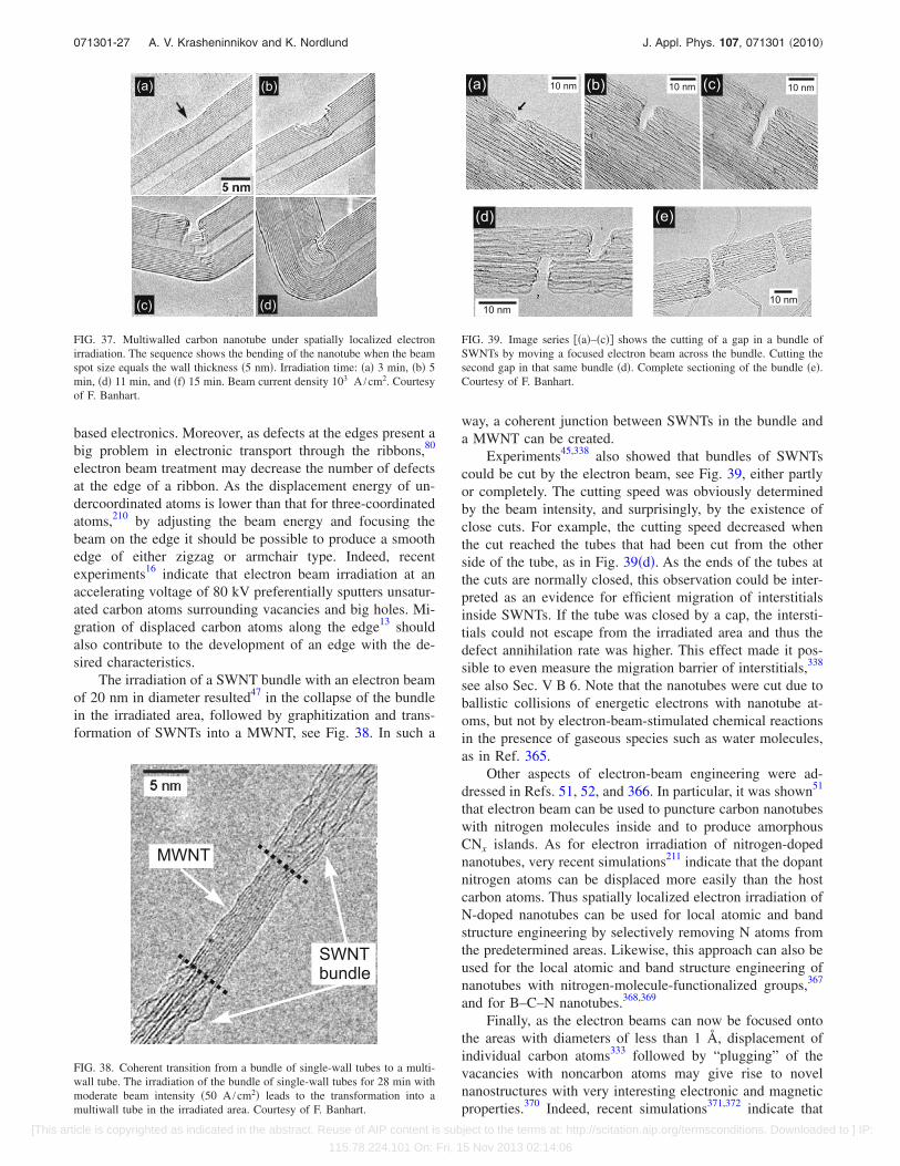
based electronics. Moreover, as defects at the edges present abig problem in electronic transport through the ribbons,80
electron beam treatment may decrease the number of defectsat the edge of a ribbon. As the displacement energy of un-dercoordinated atoms is lower than that for three-coordinatedatoms,210 by adjusting the beam energy and focusing thebeam on the edge it should be possible to produce a smoothedge of either zigzag or armchair type. Indeed, recentexperiments16 indicate that electron beam irradiation at anaccelerating voltage of 80 kV preferentially sputters unsatur-ated carbon atoms surrounding vacancies and big holes. Mi-gration of displaced carbon atoms along the edge13 shouldalso contribute to the development of an edge with the de-sired characteristics.
The irradiation of a SWNT bundle with an electron beamof 20 nm in diameter resulted47 in the collapse of the bundlein the irradiated area, followed by graphitization and trans-formation of SWNTs into a MWNT, see Fig. 38. In such a
way, a coherent junction between SWNTs in the bundle anda MWNT can be created.
Experiments45,338 also showed that bundles of SWNTscould be cut by the electron beam, see Fig. 39, either partlyor completely. The cutting speed was obviously determinedby the beam intensity, and surprisingly, by the existence ofclose cuts. For example, the cutting speed decreased whenthe cut reached the tubes that had been cut from the otherside of the tube, as in Fig. 39�d�. As the ends of the tubes atthe cuts are normally closed, this observation could be inter-preted as an evidence for efficient migration of interstitialsinside SWNTs. If the tube was closed by a cap, the intersti-tials could not escape from the irradiated area and thus thedefect annihilation rate was higher. This effect made it pos-sible to even measure the migration barrier of interstitials,338
see also Sec. V B 6. Note that the nanotubes were cut due toballistic collisions of energetic electrons with nanotube at-oms, but not by electron-beam-stimulated chemical reactionsin the presence of gaseous species such as water molecules,as in Ref. 365.
Other aspects of electron-beam engineering were ad-dressed in Refs. 51, 52, and 366. In particular, it was shown51
that electron beam can be used to puncture carbon nanotubeswith nitrogen molecules inside and to produce amorphousCNx islands. As for electron irradiation of nitrogen-dopednanotubes, very recent simulations211 indicate that the dopantnitrogen atoms can be displaced more easily than the hostcarbon atoms. Thus spatially localized electron irradiation ofN-doped nanotubes can be used for local atomic and bandstructure engineering by selectively removing N atoms fromthe predetermined areas. Likewise, this approach can also beused for the local atomic and band structure engineering ofnanotubes with nitrogen-molecule-functionalized groups,367
and for B–C–N nanotubes.368,369
Finally, as the electron beams can now be focused ontothe areas with diameters of less than 1 Å, displacement ofindividual carbon atoms333 followed by “plugging” of thevacancies with noncarbon atoms may give rise to novelnanostructures with very interesting electronic and magneticproperties.370 Indeed, recent simulations371,372 indicate that
FIG. 37. Multiwalled carbon nanotube under spatially localized electronirradiation. The sequence shows the bending of the nanotube when the beamspot size equals the wall thickness �5 nm�. Irradiation time: �a� 3 min, �b� 5min, �d� 11 min, and �f� 15 min. Beam current density 103 A /cm2. Courtesyof F. Banhart.
FIG. 38. Coherent transition from a bundle of single-wall tubes to a multi-wall tube. The irradiation of the bundle of single-wall tubes for 28 min withmoderate beam intensity �50 A /cm2� leads to the transformation into amultiwall tube in the irradiated area. Courtesy of F. Banhart.
FIG. 39. Image series ��a�–�c�� shows the cutting of a gap in a bundle ofSWNTs by moving a focused electron beam across the bundle. Cutting thesecond gap in that same bundle �d�. Complete sectioning of the bundle �e�.Courtesy of F. Banhart.
071301-27 A. V. Krasheninnikov and K. Nordlund J. Appl. Phys. 107, 071301 �2010�
[This article is copyrighted as indicated in the abstract. Reuse of AIP content is subject to the terms at: http://scitation.aip.org/termsconditions. Downloaded to ] IP:
115.78.224.101 On: Fri, 15 Nov 2013 02:14:06
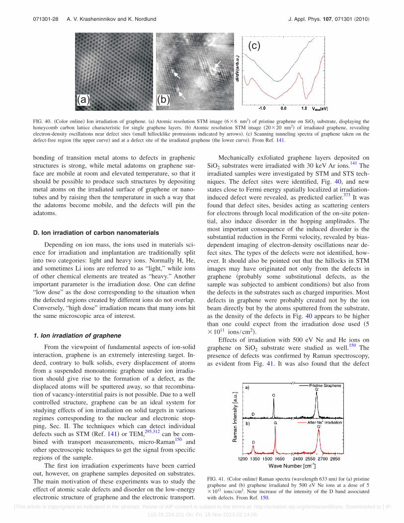
bonding of transition metal atoms to defects in graphenicstructures is strong, while metal adatoms on graphene sur-face are mobile at room and elevated temperature, so that itshould be possible to produce such structures by depositingmetal atoms on the irradiated surface of graphene or nano-tubes and by raising then the temperature in such a way thatthe adatoms become mobile, and the defects will pin theadatoms.
D. Ion irradiation of carbon nanomaterials
Depending on ion mass, the ions used in materials sci-ence for irradiation and implantation are traditionally splitinto two categories: light and heavy ions. Normally H, He,and sometimes Li ions are referred to as “light,” while ionsof other chemical elements are treated as “heavy.” Anotherimportant parameter is the irradiation dose. One can define“low dose” as the dose corresponding to the situation whenthe defected regions created by different ions do not overlap.Conversely, “high dose” irradiation means that many ions hitthe same microscopic area of interest.
1. Ion irradiation of graphene
From the viewpoint of fundamental aspects of ion-solidinteraction, graphene is an extremely interesting target. In-deed, contrary to bulk solids, every displacement of atomsfrom a suspended monoatomic graphene under ion irradia-tion should give rise to the formation of a defect, as thedisplaced atoms will be sputtered away, so that recombina-tion of vacancy-interstitial pairs is not possible. Due to a wellcontrolled structure, graphene can be an ideal system forstudying effects of ion irradiation on solid targets in variousregimes corresponding to the nuclear and electronic stop-ping, Sec. II. The techniques which can detect individualdefects such as STM �Ref. 141� or TEM,295,312 can be com-bined with transport measurements, micro-Raman150 andother spectroscopic techniques to get the signal from specificregions of the sample.
The first ion irradiation experiments have been carriedout, however, on graphene samples deposited on substrates.The main motivation of these experiments was to study theeffect of atomic scale defects and disorder on the low-energyelectronic structure of graphene and the electronic transport.
Mechanically exfoliated graphene layers deposited onSiO2 substrates were irradiated with 30 keV Ar ions.141 Theirradiated samples were investigated by STM and STS tech-niques. The defect sites were identified, Fig. 40, and newstates close to Fermi energy spatially localized at irradiation-induced defect were revealed, as predicted earlier.373 It wasfound that defect sites, besides acting as scattering centersfor electrons through local modification of the on-site poten-tial, also induce disorder in the hopping amplitudes. Themost important consequence of the induced disorder is thesubstantial reduction in the Fermi velocity, revealed by bias-dependent imaging of electron-density oscillations near de-fect sites. The types of the defects were not identified, how-ever. It should also be pointed out that the hillocks in STMimages may have originated not only from the defects ingraphene �probably some substitutional defects, as thesample was subjected to ambient conditions� but also fromthe defects in the substrates such as charged impurities. Mostdefects in graphene were probably created not by the ionbeam directly but by the atoms sputtered from the substrate,as the density of the defects in Fig. 40 appears to be higherthan one could expect from the irradiation dose used �5�1011 ions /cm2�.
Effects of irradiation with 500 eV Ne and He ions ongraphene on SiO2 substrate were studied as well.150 Thepresence of defects was confirmed by Raman spectroscopy,as evident from Fig. 41. It was also found that the defect
(a) (b)
(c)
FIG. 40. �Color online� Ion irradiation of graphene. �a� Atomic resolution STM image �6�6 nm2� of pristine graphene on SiO2 substrate, displaying thehoneycomb carbon lattice characteristic for single graphene layers. �b� Atomic resolution STM image �20�20 nm2� of irradiated graphene, revealingelectron-density oscillations near defect sites �small hillocklike protrusions indicated by arrows�. �c� Scanning tunneling spectra of graphene taken on thedefect-free region �the upper curve� and at a defect site of the irradiated graphene �the lower curve�. From Ref. 141.
FIG. 41. �Color online� Raman spectra �wavelength 633 nm� for �a� pristinegraphene and �b� graphene irradiated by 500 eV Ne ions at a dose of 5�1012 ions /cm2. Note increase of the intensity of the D band associatedwith defects. From Ref. 150.
071301-28 A. V. Krasheninnikov and K. Nordlund J. Appl. Phys. 107, 071301 �2010�
[This article is copyrighted as indicated in the abstract. Reuse of AIP content is subject to the terms at: http://scitation.aip.org/termsconditions. Downloaded to ] IP:
115.78.224.101 On: Fri, 15 Nov 2013 02:14:06
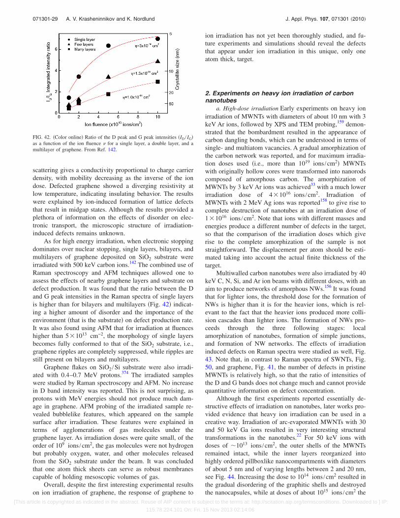
scattering gives a conductivity proportional to charge carrierdensity, with mobility decreasing as the inverse of the iondose. Defected graphene showed a diverging resistivity atlow temperature, indicating insulating behavior. The resultswere explained by ion-induced formation of lattice defectsthat result in midgap states. Although the results provided aplethora of information on the effects of disorder on elec-tronic transport, the microscopic structure of irradiation-induced defects remains unknown.
As for high energy irradiation, when electronic stoppingdominates over nuclear stopping, single layers, bilayers, andmultilayers of graphene deposited on SiO2 substrate wereirradiated with 500 keV carbon ions.142 The combined use ofRaman spectroscopy and AFM techniques allowed one toassess the effects of nearby graphene layers and substrate ondefect production. It was found that the ratio between the Dand G peak intensities in the Raman spectra of single layersis higher than for bilayers and multilayers �Fig. 42� indicat-ing a higher amount of disorder and the importance of theenvironment �that is the substrate� on defect production rate.It was also found using AFM that for irradiation at fluenceshigher than 5�1013 cm−2, the morphology of single layersbecomes fully conformed to that of the SiO2 substrate, i.e.,graphene ripples are completely suppressed, while ripples arestill present on bilayers and multilayers.
Graphene flakes on SiO2 /Si substrate were also irradi-ated with 0.4–0.7 MeV protons.374 The irradiated sampleswere studied by Raman spectroscopy and AFM. No increasein D band intensity was reported. This is not surprising, asprotons with MeV energies should not produce much dam-age in graphene. AFM probing of the irradiated sample re-vealed bubblelike features, which appeared on the samplesurface after irradiation. These features were explained interms of agglomerations of gas molecules under thegraphene layer. As irradiation doses were quite small, of theorder of 109 ions /cm2, the gas molecules were not hydrogenbut probably oxygen, water, and other molecules releasedfrom the SiO2 substrate under the beam. It was concludedthat one atom thick sheets can serve as robust membranescapable of holding mesoscopic volumes of gas.
Overall, despite the first interesting experimental resultson ion irradiation of graphene, the response of graphene to
ion irradiation has not yet been thoroughly studied, and fu-ture experiments and simulations should reveal the defectsthat appear under ion irradiation in this unique, only oneatom thick, target.
2. Experiments on heavy ion irradiation of carbonnanotubes
a. High-dose irradiation Early experiments on heavy ionirradiation of MWNTs with diameters of about 10 nm with 3keV Ar ions, followed by XPS and TEM probing,159 demon-strated that the bombardment resulted in the appearance ofcarbon dangling bonds, which can be understood in terms ofsingle- and multiatom vacancies. A gradual amorphization ofthe carbon network was reported, and for maximum irradia-tion doses used �i.e., more than 1019 ions /cm2� MWNTswith originally hollow cores were transformed into nanorodscomposed of amorphous carbon. The amorphization ofMWNTs by 3 keV Ar ions was achieved33 with a much lowerirradiation dose of 4�1016 ions /cm2. Irradiation ofMWNTs with 2 MeV Ag ions was reported158 to give rise tocomplete destruction of nanotubes at an irradiation dose of1�1016 ions /cm2. Note that ions with different masses andenergies produce a different number of defects in the target,so that the comparison of the irradiation doses which giverise to the complete amorphization of the sample is notstraightforward. The displacement per atom should be esti-mated taking into account the actual finite thickness of thetarget.
Multiwalled carbon nanotubes were also irradiated by 40keV C, N, Si, and Ar ion beams with different doses, with anaim to produce networks of amorphous NWs.156 It was foundthat for lighter ions, the threshold dose for the formation ofNWs is higher than it is for the heavier ions, which is rel-evant to the fact that the heavier ions produced more colli-sion cascades than lighter ions. The formation of NWs pro-ceeds through the three following stages: localamorphization of nanotubes, formation of simple junctions,and formation of NW networks. The effects of irradiationinduced defects on Raman spectra were studied as well, Fig.43. Note that, in contrast to Raman spectra of SWNTs, Fig.50, and graphene, Fig. 41, the number of defects in pristineMWNTs is relatively high, so that the ratio of intensities ofthe D and G bands does not change much and cannot providequantitative information on defect concentration.
Although the first experiments reported essentially de-structive effects of irradiation on nanotubes, later works pro-vided evidence that heavy ion irradiation can be used in acreative way. Irradiation of arc-evaporated MWNTs with 30and 50 keV Ga ions resulted in very interesting structuraltransformations in the nanotubes.22 For 50 keV ions withdoses of �1013 ions /cm2, the outer shells of the MWNTsremained intact, while the inner layers reorganized intohighly ordered pillboxlike nanocompartments with diametersof about 5 nm and of varying lengths between 2 and 20 nm,see Fig. 44. Increasing the dose to 1014 ions /cm2 resulted inthe gradual disordering of the graphitic shells and destroyedthe nanocapsules, while at doses of about 1015 ions /cm2 the
FIG. 42. �Color online� Ratio of the D peak and G peak intensities �ID / IG�as a function of the ion fluence for a single layer, a double layer, and amultilayer of graphene. From Ref. 142.
071301-29 A. V. Krasheninnikov and K. Nordlund J. Appl. Phys. 107, 071301 �2010�
[This article is copyrighted as indicated in the abstract. Reuse of AIP content is subject to the terms at: http://scitation.aip.org/termsconditions. Downloaded to ] IP:
115.78.224.101 On: Fri, 15 Nov 2013 02:14:06

graphitic shells collapsed into the hollow, resulting in theformation a homogeneous amorphous rod. Irradiating nano-tubes with 30 keV ions gave similar results, but at higherdoses.
The formation of similar bamboolike structures inMWNTs irradiated with 4 MeV Cl2+ ions with a dose of 3�1016 ions /cm2 was reported34 as well. In addition to thechanges in the shape of the tubes, irradiation resulted in theirswelling, as a result of which the average diameter of thetubes increased from 70 to 180 nm, possibly due to interca-lation of Cl atoms and due to defect-mediated changes in theatomic structure. Both Ga and Cl ion high dose irradiationfully amorphized the samples, as evident from the TEM im-ages, as well as from growing resistance of the tubes andincrease in the area ratio of D-peak to G-peak in the Ramanspectra.34
Self-irradiation with 100 eV C+ ions was used for mak-ing nanotube-amorphous diamond nanocomposites35 inwhich conducting mats of SWNTs were protected againstwear by 50 nm amorphous diamond films. Experiments alsoindicate that magnetized-plasma ion irradiation can be used
for encapsulating fullerenes376 and intercalating cesium in-side SWNTs �Ref. 377� via irradiation-induced defects in thetube walls.
10 and 30 keV focused beams of Ga ions were shown23
to be able to thin, slice, and alter the structure and composi-tion of MWNTs at precise locations along the nanotube axis.This strategy of harnessing ion-beam-induced defect genera-tion and doping could be attractive for modulating chemicaland electrical properties along the nanotube length, and fab-ricating nanotube heterostructures, and networks for deviceapplications.
An interesting irradiation-assisted way for manufactur-ing nanotube networks consisting of perfectly straight andsuspended structures was demonstrated.27 SWNTs grownsuspended between pillars of Si /SiO2 structures were irradi-ated with 30 keV Ga+ ions. The typical ion dose was around1.5�1014 ions /cm2. The nanotubes were straightened byion beam scans. In addition, the ion irradiation selectivelyremoved nanotubes lying on the substrate, leaving the sus-pended nanotubes in place. Although ion irradiation inducesstructural modifications to nanotubes and introduces defectsinto the nanotube lattice, the form, and dimensions of thenanotubes remained close to those of the original structures.
Irradiation-induced enhancement in the field emissionproperties of nanotubes has been reported.28 Argon irradia-tion treatment straightened as-grown curly nanotubes, seeFig. 45, similarly to Ga ion irradiation.27 As a result, the
FIG. 44. TEM micrograph of a pristine MWNT and a MWNT irradiatedwith a 5�1015 ions /cm2 dose of 30 keV Ga ions. From Ref. 22.
FIG. 43. �Color online� Typical Raman spectra of the as-grown MWNTsand MWNTs irradiated with Ar ion beam with different doses: �a� as-grown,�b� 5�1014 ions /cm2, �c� 1�1015 ions /cm2, �d� 5�1015 ions /cm2, �e� 1�1016 ions /cm2, �f� 5�1016 ions /cm2, �g� 1�1017 ions /cm2, and �h� 5�1017 ions /cm2. Compare to Raman spectra of irradiated SWNTs, Fig. 50and graphene, Fig. 41. From Ref. 156.
FIG. 45. SEM images of nanotubes �a� before and �b� after Ar ion irradiation. Nanotubes were straightened by the ion beam. From Ref. 28.
071301-30 A. V. Krasheninnikov and K. Nordlund J. Appl. Phys. 107, 071301 �2010�
[This article is copyrighted as indicated in the abstract. Reuse of AIP content is subject to the terms at: http://scitation.aip.org/termsconditions. Downloaded to ] IP:
115.78.224.101 On: Fri, 15 Nov 2013 02:14:06

local electric field was enhanced due to the increased aspectratio and reduced mutual shield effect. Additional contribu-tions may have come from irradiation-induced defects,which made nanotube effective surfaces more active, thusemitting more electrons. The electron field emission fromnanotubes has also been enhanced by Si ion beamirradiation.378 The irradiation-induced defects and the ad-sorbed molecules on the nanotubes were responsible for theenhancement of electron field emission. Thus ion irradiationappears to be a tool to improve the electron field emissionproperties of carbon nanotubes.
As for the beneficial effects of ion irradiation on nano-tube electronic properties, spatially localized Ar ion irradia-tion �with doses up to �1016 ions /cm2� of individualMWNTs deposited on SiO2 substrates was used25,379 to cre-ate a defective region which worked as a potential tunnelbarrier for electrons in the MWNT, Fig. 46. A fast increase inthe tube resistance with the irradiation dose was reported. Itwas demonstrated that a double-barrier structure fabricatedby such method can work as a quantum dot. However, thetypes of defect and their spatial distribution were not identi-fied, although knowing this is important for understandingthe Coulomb oscillations observed in the system and how thecurrent flows through the damaged MWNT shells. Spatiallylocalized ion irradiation was also used for the fabrication of asingle-electron inverter in MWNTs.26
Because irradiation-induced defects normally increasethe reactivity of nanotubes �e.g., due to dangling bonds at thesurface defects�, focused-ion-beam irradiation, followed bymild chemical treatment, was used to functionalize nano-tubes at preselected locations,24 Fig. 47. The bombardmentwith Ga ions having energies of 10–30 keV and with irradia-tion doses of �1015–1017 ions /cm2 resulted in the desiredeffect. Controlled chemical modification was also achievedwith 2 keV argon ions,29 but at much smaller doses of about
�1013 ions /cm2. The lower doses may, however, give acomparable number of surface defects, as the production ofdefects at the nanotube surface should drop with increasingion energy, see Sec. V A. Ion-beam-assisted functionaliza-tion can also be used380 for the modification of grapheneproperties.
Effects of ion irradiation were also studied by Ramanspectroscopy in DWNTs.151 As this method allows one todifferentiate signals from the outer and inner shells of aDWNT, the differences in the response of the shells to irra-diation could be probed. Highly pure DWNTs were irradi-ated with 170 keV Si and 100 keV C ions. The bombardmentwas performed at room temperature with ion doses rangingbetween 113 and 1�1015 ions /cm2. As expected, heavier Siions created more disorder than C for the same irradiationdose. As in other works discussed above, the “D-band” in-tensity increased, while the “G-band” intensity decreasedwith the dose, indicating increased lattice disorder. With in-creasing ion dose, the radial breathing modes �RBMs� of theouter tubes disappeared before the respective RBM bandsfrom the inner tubes, suggesting that the outer nanotubes aremore affected than the inner nanotubes by the ion irradiation.After Si ion bombardment to a dose of 1�1015 ions /cm2,the Raman spectrum resembled that of highly disorderedgraphite, indicating that the lattice structures of the inner andouter nanotubes were almost completely destroyed. How-ever, laser annealing partially restored the crystalline struc-ture of the nanotubes, as evidenced by the re-emergence ofthe G and RBM bands and the significant attenuation of theD band in the Raman spectrum.
SiO /Si substrate2
sour
ce
drain
Focusedion beam
CNTCNT
defected areas
(a)
(b)
FIG. 46. �Color online� Using ion irradiation for making nanotube-basedelectronic devices. �a� Schematic illustration of the fabrication of a quantumdot in a carbon nanotube by using FIBs. �b� Contour plots of source-draincurrents for the system shown in �a� at room temperature as functions ofsource-drain voltage after ion bombardment. The arrows indicate theirradiation-induced features corresponding to the Coulomb blockade regime.Reprinted from Ref. 379.
FIG. 47. �Color online� Ion-beam-assisted site-selective functionalization ofcarbon nanotubes. �a� Schematic illustration of the experimental setup. �b�Immobilization of Au nanoparticles on ion irradiated regions of carbonnanotubes. Reprinted from Ref. 24.
071301-31 A. V. Krasheninnikov and K. Nordlund J. Appl. Phys. 107, 071301 �2010�
[This article is copyrighted as indicated in the abstract. Reuse of AIP content is subject to the terms at: http://scitation.aip.org/termsconditions. Downloaded to ] IP:
115.78.224.101 On: Fri, 15 Nov 2013 02:14:06

b. Low-dose irradiation Effects of single ion impacts onthe atomic structure and properties of nanotubes can be stud-ied by low-dose ion irradiation combined with other tech-niques that can detect signatures of irradiation-induceddefects.
MWNTs dispersed on a graphite substrate wereirradiated32 with 30 keV ions with a dose of around1011 ions /cm2. STM measurements carried out under ambi-ent conditions revealed hillocklike protrusions on the nano-tube walls �Fig. 48�, which were associated with individualvacancies, in agreement with the theoreticalpredictions.174,381,382 Annealing in nitrogen atmosphere of theirradiated samples at 450 °C demonstrated that defects innanotubes tend to heal already at moderate temperatures,which was in line with the TEM results.72
Low dose irradiation of individual SWNTs with 120 eVAr ions �this energy is just above the threshold to producedefects in SWNT, see Sec. V A� and electronic transportmeasurements on the irradiated nanotube made it possible toassess the effect of individual defects on nanotubeconductance.11 At such low energies, irradiation with Ar ionsshould result in the formation of single and DVs, which giverise to a dramatic drop in the conductance of the nanotubedue to the 1D nature of the system and thus a very smallnumber of conduction channels. Theoretical transport calcu-lations showed that mostly DVs contribute to the resistanceincrease and that just 0.03% of DVs produced an increase ofthree orders of magnitude in the resistance of a 400 nm longSWNT.
The impact of low-dose ��1012 ions /cm2� ion irradia-tion on bundles of SWNTs was experimentally studied aswell.21 The bundles were irradiated with an 500 eV Ar+ ionbeam followed by transport measurements. The results sug-gest that irradiation gives rise to current redistribution be-tween the damaged and undamaged tubes in the same rope,which can be interpreted as evidence for the formation ofirradiation-mediated links between individual SWNTs in thebundle. The links appear to be of the same origin as theintertube links in electron-irradiated nanotube bundles.10,48
The formation of covalent bonds between bundled-up nano-tubes under impacts of low energy �below 50 eV� CF3
+ ionswas also reported.30 The cross-links, however, should appearonly near the bundle surface at such low ion energies.
Low dose ion irradiation has also been used to alter thecharacteristics of nanotube bucky paper �NBP� �see also Sec.V F 1�. A remarkable correlation between frequency shifts inG+, D, and D� Raman modes and changes in the conductivityand Young’s modulus of freestanding SWNT networks wasfound167 �Fig. 49�. Under 30 keV Ar ion irradiation with
FIG. 48. MWNTs with defects �hillocklike protrusions� created by Ar ion irradiation �a�. Atomic resolution STM image of a nanotube defect �b�. From Ref.32.
FIG. 49. �Color online� �a� Fractional increase of electrical conductivity andYoung’s modulus of a piece of an SWNT paper sample relative to theirvalues before irradiation with low doses of Ar ions. �b� Fractional shifts inthe frequencies of Raman D �1310 cm−1�, G+ �1585 cm−1�, and D�
�2600 cm−1� modes of a piece of the same sample, as a function of Arirradiation dose. The lines in �a� and �b� join the data points �the lines on theright extrapolate to data points at a dose of 5.5�1012 ions /cm2�. �c� In-crease in the intensity ratio I�d�/I�g� for the D and G modes on irradiation.From Ref. 167.
071301-32 A. V. Krasheninnikov and K. Nordlund J. Appl. Phys. 107, 071301 �2010�
[This article is copyrighted as indicated in the abstract. Reuse of AIP content is subject to the terms at: http://scitation.aip.org/termsconditions. Downloaded to ] IP:
115.78.224.101 On: Fri, 15 Nov 2013 02:14:06

doses up to 5.5�1012 ions /cm2, all these properties showsimilar peaks as a function of irradiation dose. Small irradia-tion doses gave rise to an increase in conductivity and me-chanical properties of the sample, which could be interpretedas evidence for irradiation-induced interconnection of nano-tubes or functionalization of SWNTs at irradiation-induceddefects by various chemical species due to the contacts withair accompanied by chemical doping. Experiments383 alsoindicated that thermal annealing of tunneling barriers be-tween individual nanotubes by heat released during colli-sions of energetic ions with the target atoms may be a pos-sible reason for the improvement in conducting properties,although irradiation-mediated adsorption/desorption of vari-ous molecules and cross-linking could also contribute to theobserved changes in conductivity. Although the role of ionbeam heating on the SWNT mats and their Raman spectra,Fig. 50, has been studied375 later on, the reason for the ob-served increase in mechanical properties and conductivityremains unclear, as both functionalization and cross-linkingmay contribute to the observed phenomena.
3. Light ions: Proton irradiation of carbon nanotubes
Several experiments36–38,384 on irradiation of SWNTswith high energy �a couple of MeV range� protons were re-cently carried out. Both purified SWNTs36,37 and those as-sembled as a NBP385–387 representing a highly interconnectednetwork of SWNT bundles384 were irradiated. Effects of pro-ton irradiation on nanotubes embedded into a polymer matrixwere studied as well.38 In addition to fundamental aspects ofenergetic proton interactions with highly anisotropic carbon-based nanomaterials, the interest in the response of nano-tubes to proton irradiation was stimulated by the possible useof nanotubes in space applications, in particular, as compo-nents of solar cells.384
SWNTs deposited onto TEM grids for subsequent analy-sis were irradiated36 in air at room temperature with 3 MeVprotons with doses ranging from 6 �C to 0.72 mC, or cor-respondingly, from 1.2�1013 to 3�1016 protons /cm2 �thebeam diameter was reported to be 4 mm�. Evident morpho-logical changes such as curving of SWNTs and formation ofshort pieces were observed at doses of about 0.1 mC. Further
irradiation resulted in nearly full amorphization of the nano-tubes �a significant fraction of the tubes were still present aspieces of different lengths�. Based on the results of the ex-periments, it was concluded that for the typical near-Earthspace condition during “quiet sun” periods �typical protonenergies of around 1 GeV, much lower fluxes� SWNTs willundergo no detectable alterations for practically unlimitedtime.
A 0.5 �m thick SWNT film and a similar one placedbelow a 16.75 �m Xe film were irradiated at 15 K with 1MeV protons.37 The maximum irradiation doses were 9.6�1014 and 5.5�1014 protons /cm2, respectively. The analy-sis of the irradiated samples done by Fourier transform in-frared and Raman spectroscopy evidenced formation of CHbonds and defects in nanotubes, accompanied by somechanges in nanotube diameters.
Effects of proton irradiation on optical properties ofSWNTs matrixed in poly�3-octylthiophene� wereinvestigated38 by an optical absorption technique. Two inter-band transitions were observed, at 0.71 and 1.28 eV in asample that was subject to 2 MeV proton irradiation to flu-ences ranging between 5.0�1010 and 5.6�1015 protons /cm2. The results indicate that proton irradia-tion to fluences as high as 5.6�1015 has little effect on theinterband transitions in carbon nanotubes. However, smallradiation-related degradation has been observed as judged bythe broadening of the interband transition spectra and by thereduction of the RBM intensity observed by Raman scatter-ing.
The radiation tolerance of NBP was also analyzed in thecontext of the application of nanotubes in space photovoltaicapplications in combination with quantum dots.384 Irradiationwith 2 MeV protons caused the room temperature resistivityof the NBP samples to increase nearly linearly up to a flu-ence of 7�1016 protons /cm2. Based on the comparison ofthe irradiation-induced changes in NBP resistivity �the de-fects in the samples were not characterized at the micro-scopic level�, it was concluded that the sensitivity of thenanotube paper falls between that of individual nanotubesand graphite. This was a somewhat unexpected result, forsystems such as NBP which are composed of radiation-softcomponents �recall that nanotubes are radiation-soft them-selves; irradiation dose of 3�1016 protons /cm2 resulted incomplete amorphization and fracture of SWNTs �Ref. 36��. Itwas also concluded that the solar cells based on quantumdots and NBP paper should be five orders of magnitude moreresistant to radiation damage than the conventional bulk so-lar cells.
As seen from the experimental results, irradiation doses�1017 protons /cm2 should completely amorphize thesamples. However, the estimates of the radiation damage inSWNT created by protons with such energies and doses us-ing the TRIM code177 give dpa �displacement per atom� val-ues of around 10−4 �Ref. 388�. This value means that onaverage, one atom out of 10 000 was displaced during irra-diation. Obviously, this is not enough for sample amorphiza-tion, and the nuclear stopping can be excluded. The elec-tronic stopping for 1 MeV protons is some two to threeorders of magnitude larger than the nuclear one, but the
FIG. 50. �Color online� Raman spectra of an unirradiated SWNTs sampleand of samples irradiated by 30 keV N ions with different irradiation doses.Resonant breathing modes �left panel� and the D �1300 cm−1� and the G�1590 cm−1� bands �right panel�. From Ref. 375.
071301-33 A. V. Krasheninnikov and K. Nordlund J. Appl. Phys. 107, 071301 �2010�
[This article is copyrighted as indicated in the abstract. Reuse of AIP content is subject to the terms at: http://scitation.aip.org/termsconditions. Downloaded to ] IP:
115.78.224.101 On: Fri, 15 Nov 2013 02:14:06

nanotubes are excellent heat and charge conductors, so thatthe deposited energy should be quickly redistributed over thesample. Note that for the typical metals such as copper irra-diated with light ions, the TRIM code gives dpa values182
which are at least in qualitative agreement with the experi-ments. Although chemically reactive species �such as waterand oxygen radicals which appear due to irradiation� may bepresent in the system and play some role, similar to irradia-tion of nanotubes with low-energy electrons365 or ultravioletlight,54 the precise mechanism of the damage creation byhigh energy protons is unknown at the moment.
4. Welding of nanotubes by ion beams
As discussed in Sec. V C 5, a focused electron beam canbe used18 for welding nanotubes together at high tempera-tures. As MD simulations389 pointed out, ion irradiation com-bined with high-temperature annealing should also result inwelding of crossed nanotubes, both suspended and depositedon substrates, see Fig. 51. For the latter, the optimum Ar ionenergies were predicted to be about 0.5 keV, whereas theoptimum irradiation doses should be about 1015 ions /cm2.Higher doses will result in heavy damage of the carbonnetwork.389
The theoretical predictions were corroborated later on byexperiments. Irradiation of overlapping nanotubes with 10keV Ga ions with doses up to 1016 ions /cm2 resulted in thewelding of nanotubes,23 see Fig. 52. Similar results wereobtained with 50 keV carbon ions,390 although the irradiation
dose of 1015 ions /cm2 used converted the tubes into amor-phous rods. As the experiments,23,390 were carried out atroom temperature, irradiation of nanotubes at higher tem-peratures and/or subsequent annealing should minimize theamount of damage in the nanotubes.
The welding of the MWNTs has been realized at el-evated temperature by 40 keV Si ion beam irradiation.391 Itwas found that both the irradiation dose and temperaturegreatly affect the welding of the MWNTs. At the irradiationdose of 5�1016 Si ions /cm2, the formed MWNT junctionshad well-ordered structure at the temperature range of 600–850 K. This work gives another confirmation that ion irra-diation technology combined with heating can be used forinterconnecting nanotubes in future nanodevices.
5. Ion-irradiation-induced links between nanotubesand substrates
As simulations predict,175,270 ion irradiation of supportednanotubes should result in the pinning of the nanotubes tometallic and graphite175 substrates, as well as to Si �Ref. 270�surfaces. This should happen through the formation ofchemical bonds between the nanotube and substrate atomsnear irradiation-induced defects �by saturating danglingbonds�, thus increasing the nanotube-substrate adhesion.
MWNTs were experimentally welded to SiNsubstrates.23 The experiments392 also showed that electricalcontact resistance of MWNTs deposited on gold contact fin-gers can be decreased by orders of magnitude when the con-tact areas are selectively exposed to the electron beam in aSEM. The local focused electron beam irradiation was alsoreported393 to make good thermal contacts between the nano-tubes and platinum nanofilm sensors. Thus one may hopethat ion irradiation will improve not only mechanical but alsoelectronic/thermal properties at the interfaces between thetubes and the environment.
6. Irradiation-mediated doping of carbon nanotubeswith foreign atoms
Chemical doping of nanostructured carbon systems suchas carbon nanotubes, fullerenes, and peapods is a possibleroute toward controllable modification of their structural,mechanical, and, first of all, electronic properties. Dopingmay be implemented by intercalating foreign atoms into theopen space in the carbon network394–396 or by substitutingthe host atoms with impurities.218,397–405
As for substitutional doping, much attention has recentlybeen given to the doping of nanotubes with boron and nitro-gen atoms. This is a natural choice of the dopant, as B and Natoms are the neighbors of C in the Periodic Table and thushave roughly the same atomic radius as C, while they pos-sess one electron less or more than C, respectively. Severalmethods based on arc-discharge techniques399,406 and substi-tutional reactions401 have been developed for doping. Unfor-tunately, instead of occupying the substitutional sp2 positionin the graphitic network, a substantial part of the dopant ischemisorbed407 on the nanotube surface or binds to irregularcarbon structures in sp3 sites.399 Problems with incorporating
FIG. 51. Two crossed carbon nanotubes before irradiation �a�. Atomic net-works of �10,10�&�12,0� and �10,10�&�10,10� nanotubes �panels �b� and �c�,respectively� welded together by energetic Ar ions, as simulated �Ref. 389�with the EP MD method.
FIG. 52. SEM micrographs of overlapping nanotubes marked A and B, �a�prior to irradiation, and after exposure to �b� 1016 and �c� 2�1016 ions /cm2 of 10 keV Ga ions. �d� An example of a nanotube networkformed by several welds indicated by arrows. �e� SEM micrograph showinga nanotube welded to the edge of the SiN membrane �see the arrows� byexposure to 1017 ions /cm2 of 30 keV Ga ions. From Ref. 23.
071301-34 A. V. Krasheninnikov and K. Nordlund J. Appl. Phys. 107, 071301 �2010�
[This article is copyrighted as indicated in the abstract. Reuse of AIP content is subject to the terms at: http://scitation.aip.org/termsconditions. Downloaded to ] IP:
115.78.224.101 On: Fri, 15 Nov 2013 02:14:06

B atoms into the carbon lattice of nanotubes have also beenreported.406 All of these issues further limit the applicabilityof these techniques.
Low-energy ion-irradiation was suggested267,408 as an al-ternative way to introduce B/N impurities into nanotubes.The simulations267,408 showed that up to 40% of the imping-ing ions can occupy directly the sp2 positions in the nanotubeatomic network. Ion beams have been successfully used toimplant N+ ions into graphite409 and fullerene solids,410 sothe technique was also expected to work with nanotubes.
Indeed, doping of nanotubes with N atoms through irra-diation was implemented experimentally.31,411–413 SWNTswere bombarded with low energy �70 eV �Ref. 411� and 500eV �Ref. 31�� N2
+ ions. XPS experiments showed that the N1s core level spectra for N-doped nanotubes could be inter-preted in terms of two peaks related to sp2 and sp3 hybrid-ization of N atoms in the C network. AFM nanoindentationof the irradiated tubes also provided evidence for the appear-ance of sp3-hybridized bonds, as manifested by an increasein hardness. Overall, the experimental results were in linewith the theoretical predictions.267,408 Overall, the results in-dicated that irradiation-mediated doping of nanotubes is apromising way to control the nanotube electronic and evenmechanical properties due to impurity-stimulated cross-linking of nanotubes.
In addition to substitutional doping, MD simulations268
also demonstrated that intercalation of K atoms into the openspace of nanotubes can be achieved by means of irradiation.The formation of clusters from the implanted potassium at-oms was studied as well. It was found that for MWNTs withone to three shells, the highest ratio of K atoms in clustersper total number of K ions should be obtained at irradiationenergy of about 100 eV. Such low energies should also mini-mize the damage created in nanotubes by energetic ions.
7. Carbon nanotubes as masks against ionirradiation
Another quite interesting application of irradiation ofnanotubes on metallic substrates has been reported. Experi-ments demonstrated that ion bombardment and nanotubesmay be employed for fabricating metal NWs using MWNTsas masks.414 By irradiating with 300 eV Ar+ ions, a Au/Tiwire about 10 nm in width has been formed underneath aMWNT lying on a thin Au/Ti layer deposited earlier on aSiO2 substrate.414 The key idea is illustrated in Fig. 53.
After forming the NW due to metal layer sputtering ev-erywhere except for the area beneath the nanotube, theMWNT could be removed by an atomic force microscope�AFM� or dissolved. Because nanotubes are micrometer-longand nanometer-wide objects and since they can be positionedvery accurately using the AFM by pushing themmechanically,415 the described technique may potentially beemployed for developing a large and complicated network ofmetal NWs.
A computational study281 was done to estimate the the-oretical limit for the minimum width of a metal NW whichcould be produced using this method. MD simulations of Arion irradiation of MWNTs showed that the bombardment re-sults in the sputtering of carbon atoms from the MWNT,
formation of vacancies on the MWNT walls, and insertion ofinterstitial atoms between the shells. High irradiation doseslead to the complete amorphization of the MWNT, but theamount of sp3 bonds is very small, which is in agreementwith experimental results.159 By estimating the sputteringyield from a MWNT �notice that the yield is lower for car-bon than for typical metals� and taking into account thethickness of the metal layer, a universal equation was derivedwhich for a given NW material allows one to estimate thetheoretical limit on the minimum width of the wire as afunction of the original thickness of the metal layer. It wasshown that this technique potentially provides a better reso-lution than the present-day electron beam lithography, al-though a low AFM operation speed prevents mass produc-tion of metal wires using nanotubes as masks against ionbombardment.
This setup may also be used for spatially selective ionimplantation into the parts of the sample which have notbeen covered with nanotubes. Thus, the threshold energy ofincident ions �the maximum energy at which no energeticrecoil hit the area below the nanotube� is an important char-acteristic. The threshold energy as a function of the MWNTouter diameter �number of shells� was evaluated281 for vari-ous MWNTs. The threshold energy was found to grow lin-early with the number of shells, see Fig. 53�c�. An analyticalapproximation was derived which makes it possible to esti-mate the minimum diameter of a MWNT needed to preventthe substrate below the MWNT from sputtering and ion im-plantation for a given energy of the incident ion.
8. Channeling of ions in nanotubes
The tubular shape of carbon nanotubes, as well as theirhollow cores, high aspect ratio, and a low concentration ofdefects suggest another possible application for nanotubes:conduits for energetic ions.
This potential application of nanotubes is related to aphenomenon which is important for present-day semicon-
FIG. 53. Schematic illustration of the setup for using MWNTs as masksagainst ion bombardment. �a� Before irradiation, a nanotube has been de-posited on a thin metal layer on a SiO2 substrate. Ion irradiation results insputtering of metal atoms and nanotube amorphization. �b� After irradiationthe nanotube can be removed by AFM. �c� Threshold energy of incident ions�the maximum energy at which no energetic recoil hit the area below thenanotube� as a function of tube outer diameter �number of shells�.
071301-35 A. V. Krasheninnikov and K. Nordlund J. Appl. Phys. 107, 071301 �2010�
[This article is copyrighted as indicated in the abstract. Reuse of AIP content is subject to the terms at: http://scitation.aip.org/termsconditions. Downloaded to ] IP:
115.78.224.101 On: Fri, 15 Nov 2013 02:14:06

ductor technology:84,416 channeling of energetic ions throughsolids. When an energetic ion moves nearly parallel to amajor axis or plane in a single crystal, it can be steered downthe open channel between the aligned rows of atoms, therebyavoiding violent collisions with the host atoms and givingrise to deeper implantation and less lattice disorder.
The channeling of heavy ions with keV energies throughMWNTs was theoretically studied417–419 by MD simulationsand within the framework of the classic electromagnetictheory.420 It was shown that under certain conditions of thetube alignment with respect to the ion beam and of ion en-ergies, the ions can efficiently channel through the emptycores of the nanotubes. Suggestions were made for making ananotube-based conduit for energetic ions, which shouldwork as an aperture and allow one to manipulate ion beamsat the nanoscale, see Fig. 54. Note also that nanotubes havebeen suggested as possible conduits for atoms and moleculeswith thermal energies.421–423 Extensions to higher energies ofthe particles might also result in developing other promisingapplications in biology and materials science. The main ex-perimental challenge would be the stability of the tubes un-der irradiation, as defect formation will result in the accumu-lation of the displaced atoms in the nanotube core, whichwill quickly block the tube for the ions. Also, wall scatteringhas high probability for stopping low energy ions.
The channeling of carbon ions in nanotube bundles hasbeen studied as well424 by classical MD. The carbon ionswere fired into the rope on the outside of the nanotubes in adirection almost parallel to the longitudinal axis. It wasfound that channeling takes place when the incidence angleis smaller than a critical angle and that the dependence of thecritical angle on the energy follows an inverse square rootfunction. The calculations also showed that the dependenceof the critical angle on the energy is very similar for intra-and intertube channeling. The dependence of the criticalangle �c on ion energy and mass was also addressed,425 andthe square root rules �c�E−1/2 and �c�M−1/2 were con-firmed.
The motion of high energy light ions �protons� throughfreestanding SWNTs426–429 and nanotubes embedded in vari-ous dielectric media430 has received even bigger attention
than that of heavy ions. The driving force for these studieswas the possibility to use SWNT bundles for steering beamsof high energy �GeV� protons, which would otherwise re-quire cumbersome and expensive magnetic systems. How-ever, despite an extensive theoretical analysis and first ex-perimental results431 it is not clear at all if nanotubes can inpractice be used for this purpose, as the sample may quicklybe destroyed by the beam, as experiments on proton irradia-tion of SWNTs indicate.
E. Irradiated carbon nanotubes and onions as high-pressure cells
Another very interesting irradiation-induced phenom-enon in carbon nanotubes and onions was recentlyreported.19,20 When the shells of carbon onions or nanotubescontract due to irradiation-induced knock out of carbon at-oms, followed by reconstructions of the atomic network �seeFig. 32�, they should inevitably exert pressure on the mate-rial encapsulated inside the shells.
Controlled electron irradiation of MWNTs was demon-strated to cause large pressure buildup within the nanotubecores that can plastically deform, extrude, and break solidmaterials that are encapsulated inside the core. It had beenearlier shown that closed-shell carbon nanostructures, suchas carbon onions, can act as self-contracting high-pressurecells under electron6 and ion284 irradiation, and that highpressure buildup in the onion cores can even induce graphite-diamond transformations �see Ref. 72 for a review�. How-ever, it was not obvious that high pressure can be achievedinside nanotubes, as the difference in the geometry �cylinderversus sphere� may have been critical for pressure buildup.
MWNTs encapsulating Fe, Fe3C, or Co NWs wereirradiated19 in a TEM with a field emission gun and an ac-celeration voltage of 300 kV at a temperature of 600 °C.Figure 55 shows the evolution of a nanotube partly filledwith a Fe3C NW under irradiation. The initial configurationis presented in Fig. 55�a� Irradiation of the section at the endof the wire leads to a nonuniform collapse of the tube. Thehollow noncollapsed part of the tube fills up with graphiticfilaments �Fig. 55�b��. Carbon material migrates from theopen side of the channel and aggregates at the end of the
am
FIG. 54. �a� Schematic representation of a beam of Ar ions colliding with amultiwalled carbon nanotube with an open end. Depending on ion energy,impact point, and angle �1, the ion hitting the inner shell of the tube caneither remain in the core region or go through the shell. �b� The basic ideafor a nanotube-based ion aperture. From Ref. 417.
FIG. 55. �Color online� Typical evolution of a MWNT partly filled with aFe3C NW under electron irradiation with an electron beam �about 60 nm indiameter, more than the area schematically shown in the figure� and200–400 A /cm2 in intensity� during a total period of 50 min at a specimentemperature of 600 °C. �a� Tube before irradiation. ��b�–�e�� Irradiationleads to a collapse of the tube and deformation of the Fe3C crystal. �f� Tubecollapse cuts off the thinned Fe3C crystal. Scale bars 5 nm. See Ref. 19 fordetails.
071301-36 A. V. Krasheninnikov and K. Nordlund J. Appl. Phys. 107, 071301 �2010�
[This article is copyrighted as indicated in the abstract. Reuse of AIP content is subject to the terms at: http://scitation.aip.org/termsconditions. Downloaded to ] IP:
115.78.224.101 On: Fri, 15 Nov 2013 02:14:06

Fe3C wire by closing the inner hollow with graphene sheets.Therefore, the number of shells increases locally. The tubenow collapses in the region of the carbide crystal by deform-ing the crystal. The diameter of the Fe3C wire decreasesfrom 9 to 2 nm while the solid carbide is squeezed throughthe hollow core downward along the tube axis, as in an ex-trusion process. The final collapse of the tube pinches andcuts off the thinned wire �Fig. 55�b��. The compressive effectis also manifested in a decrease in lattice spacing betweengraphitic shells and in the encapsulated crystal.
Qualitatively similar results were obtained for Co crys-tals. Note that the collapse of the tubes and the extrusion ofencapsulated material occurred only under electron irradia-tion, not under heating. Additional heating of the specimenby the electron beam was negligible because the rate of in-elastic energy loss of the electrons is low and nanotubes areexcellent heat conductors, so the transferred energy coulddissipate into the environment.
Atomistic computer simulations by the DFTB methodand continuum theory modeling shed light on the origin ofthe pressure. As discussed in Sec. V A 5, knock-on displace-ments of carbon atoms due to energetic electrons create va-cancies and interstitials in the nanotubes. SVs are mobileenough216 to form divacancies �see also Fig. 16�, which areenergetically favorable over SVs. DVs are essentially immo-bile even at 600 °C, as their migration energy is more than 5eV. On the contrary, carbon interstitial atoms between theshells of MWNTs are highly mobile and can easily migrateaway from the irradiated region, so it was assumed that nointerstitials were left in the irradiated area, and that only DVswere present. Calculations of the atomic structure of free-standing �without encapsulates� nanotubes with various num-bers of DVs showed contraction of the nanotube due to re-constructions of the atomic network, Fig. 56�b�. Fornanotubes encapsulating materials, this should exert pressureon the material inside. As the carbon-carbon covalent bond isvery strong, one can expect a substantial pressure buildup,before the tube breaks.
Very recently carbon onions were used as extrusioncells.20 Au, Pt, Mo, and W crystals of a few nanometers insize were encapsulated inside graphitic shells by coevapora-tion in an arc discharge432 and irradiated with electrons �300keV� in a temperature range of 300–1000 °C in the heatingstage of a TEM. Under intense electron irradiation in a widebeam, the particles became spherical due to surface stress,which is exerted by the graphitic shells upon the removal ofatoms and reconstruction. Then the electron beam was fo-cused onto a spot of 2 nm in diameter and directed onto apoint at the projected circumference of the graphitic shells.After 10–20 s, this caused a hole366 �2–3 nm in diameter�through which the material under pressure could escape.Then the beam diameter was spread again over the wholeparticle. During the continuing collapse of the shells,19,432,433
pressure was built up and the solid metal was gradually ex-truded through the hole, Fig. 57. Due to the slow contractionof graphitic shells, the deformation occurred on a scale of0.1–1 nm/s. This made it possible to study the stability ofNCs in detail under continuous load. The correlation withatomistic simulations showed that the observed slow plastic
deformation is due to dislocation activity. The results alsoprovided evidence that the vacancy concentration in a nano-scale system can be smaller than in the bulk material.
Simulations19,20 showed that pressure inside irradiatednanotubes and onions can be as high as 40 GPa, only anorder of magnitude below the pressure in the center of Earth��360 GPa� or the highest pressure that has been achievedin diamond anvil cells ��400 GPa�. However, phase trans-formations in many materials are within this range. More-over, the advantage of the technique is that the evolution ofthe system can be monitored in situ with high spatial andtemporal resolution, as the experiment is carried out insidethe TEM. This technique can also be used for creating andstudying new phases of materials which can exist only at thenanoscale and at high pressures.
Concurrently with electron irradiation of nanotubes withencapsulates, an experiment similar in spirit was carriedout.297 MWNTs with typical diameters of 20–30 nm and en-capsulating nickel nanorods were irradiated with high energy�100 MeV� Au+7 ions. TEM studies of the irradiated samples
(a) (b)
(c)
(d)
D0
DD0
D
sVsV
dV
(a)
dV
0 0.02 0.04 0.06Concentration of DVs n
0
20
40
60
Pre
ssure
Pto
t(G
Pa)
4 shells3 shells2 shells1 shell
metal
FIG. 56. �Color online� Pressure buildup inside carbon nanotubes. �a� Sche-matic cross section of a MWNT contracting �indicated by the small arrows�because of the removal of atoms from the shells �solid circles� under theelectron beam. The dashed circles indicate the shells in the pristine tube. Theinner core of the tube is filled with an incompressible material. �b� Forma-tion of DVs from SVs due to SV migration and coalescence. �c� Atomicnetworks of a pristine �10, 10� �right� and irradiated nanotube �left�. Note adecrease in the average tube diameter due to the reconstruction of the atomicnetwork near vacancies. �d� Pressure inside a SWNT and MWNTs withdifferent numbers of shells as a function of DV concentration. The hatchedarea corresponds to a high concentration of DVs, which may cause breakupof the tube walls and loss of pressure.
(b)(a)
FIG. 57. �Color online� Extrusion of metals from carbon onion due to theirradiated-induced pressure buildup. �a� TEM image of a partly extrudedgold crystal. �b� Schematic illustration of the process and simulation setup.From Ref. 20.
071301-37 A. V. Krasheninnikov and K. Nordlund J. Appl. Phys. 107, 071301 �2010�
[This article is copyrighted as indicated in the abstract. Reuse of AIP content is subject to the terms at: http://scitation.aip.org/termsconditions. Downloaded to ] IP:
115.78.224.101 On: Fri, 15 Nov 2013 02:14:06

showed that irradiation resulted in a decrease in the interpla-nar spacing of nanotube walls and nickel �111� planes. Theeffect was relatively weak, as the irradiation dose was small�of the order of 3�1013 cm−2�, and because irradiation wasdone at room temperature, which was not enough for effi-cient annealing of defects in nanotube walls, and thus highpressure was not generated. Contrary to Ref. 19, irradiation-induced defects in the metal rods were reported. This is par-ticularly interesting, as the energy loss rate in the metal�through electronic stopping� was not high enough to pro-duce defects in Ni. More studies are necessary to understandthe mechanism of damage production in the nanoscale com-posite nanotube-metal systems.
F. Influence of defects on the properties ofnanocarbon systems
1. Mechanical properties
The atomic structure of MWNTs, SWNTs in bundles,and other macroscopic forms of nanotubes such as NBP isgoverned by two kinds of atom-atom interaction: short-ranged covalent bonding between the C atoms within thegraphene planes and long-ranged vdW-type interactions be-tween atoms in different SWNTs or different shells inMWNTs. The covalent interaction is very strong; the carbon-carbon covalent bond in graphite and nanotubes is one of thestrongest bonds known. At the same time, vdW interactionsare three orders of magnitude weaker. Due to different typesof interactions and highly anisotropic atomic structure, car-bon nanotubes have anisotropic mechanical properties. Theaxial properties, such as Young’s modulus Y, are excellent�Y �1 TPa, Ref. 434�, while the properties associated withthe vdW forces �e.g., the bending modulus of a nanotubebundle10� are much worse. The strength of macroscopic ma-terials is also very low, as tubes can easily slide with respectto each other.
As shown in Sec. V B, either electron or ion irradiationresults in the formation of defects in nanotubes. These de-fects, especially vacancies, have a deleterious effect—deterioration of axial mechanical properties of nanotubes, ascomputer simulations291,354,435–438 indicate. Experiments10
showed that during electron irradiation with doses over 50�1020 e /cm2, the bending modulus started decreasing,which was understood in terms of the damage accumulationin SWNTs, and thus, a noticeable drop in the Young’s �axial�modulus of individual tubes.353,354 Simulations demonstratedthat small vacancies �from one to three missing atoms� rela-tively weakly affect Y �Ref. 354�. Due to the quasi-1D struc-ture of individual nanotubes, the effect of vacancies on thetensile strength and critical strain of nanotubes proved to bemuch stronger �20%–30%, Refs. 354 and 435�. Interestinglyenough, the theoretical fracture strength of nanotubes withpoint defects is still much higher than the experimental val-ues for supposedly pristine tubes.439 This discrepancy can beattributed435 to the presence of large-scale defects, such asthose that may arise from oxidative purification processes.Indeed, by omitting chemical treatments from the samplepreparation process, and thus avoiding the formation of de-fects, the tensile strength of MWNTs was increased by a
factor of 3 �Ref. 8� as compared to previous experiments.The measured values of about 100 GPa were close to thetheoretically predicted values of 90–120 GPa.354,435
At the same time, irradiation may give rise to irradiation-induced covalent bonds between tubes, Fig. 11. Thus, pro-vided that the drop in the axial properties is not that big, theoverall strength of the nanotube material may increase. As-suming that the axial mechanical properties remain roughlythe same under moderate irradiation, formation of covalentbonds between nanotubes in a bundle would increase theYoung’s modulus of the bundle,353 in agreement with theexperimental results,10 and its tensile strength �assuming thatonly the outermost nanotubes in the bundle are clamped andthat inner shells in pristine samples do not carry mechanicalload�. Likewise, a small amount of defects can increase theinterlayer shear strength of MWNTs by several orders ofmagnitude,440 which would have a strong effect271,441 on thefailure of nanotubes by the sword-in-sheath mechanism. Inagreement with theoretical predictions, recent experiments308
on the telescopic motion of MWNTs demonstrated thatirradiation-induced SVs at the telescopic interface lead to anincrease in friction, but annealing of defects restores smoothmotion of the sliding shells. Moreover, electron irradiation ofMWNTs at 200 keV led to improvements in the maximumsustainable loads by more than an order of magnitude.8 Thiseffect is attributed to cross-linking between the shells, so thatthe mechanical load was shared between the shells. In a stan-dard tensile strength measurement, the load is carried outonly by the outermost shell, and when it breaks, the tube isfragmented by the sword-in-sheath mechanism.
Irradiation can also increase the tensile strength of mac-roscopic nanotube products, such as NBP,266 Fig. 58. Due toa low density �or correspondingly, high porosity �80%, Ref.386� and weak interactions between the bundles, the experi-mentally measured tensile modulus, strength and strain tofailure of the NBP mats proved to be several orders of mag-nitude smaller385,387 than those for individual nanotubes.Simulations demonstrated that the stiffness and tensilestrength of NBP and nanotube fibers442–444 can be substan-tially �several orders of magnitude� increased by irradiation.Physically, an increase in stiffness is mainly due to
FIG. 58. �Color online� �a� Image of SWNT bucky paper on aluminum foilcompared in size with a 1 Euro coin. �b� SEM image of the same sample.Courtesy of K. Arstila. �c� Nanotube mats used in simulations �Ref. 266� andschematic representation of an individual bundle. �d� Molecular models ofnanotubes with irradiation-induced covalent bonds between two tubes in thesame bundle and in different bundles.
071301-38 A. V. Krasheninnikov and K. Nordlund J. Appl. Phys. 107, 071301 �2010�
[This article is copyrighted as indicated in the abstract. Reuse of AIP content is subject to the terms at: http://scitation.aip.org/termsconditions. Downloaded to ] IP:
115.78.224.101 On: Fri, 15 Nov 2013 02:14:06

irradiation-induced intertube covalent bonds at the bundlecontact areas, Fig. 58. Several experiments indeed indicatethat Young modulus of SWNT bucky paper can be increaseddue to irradiation,167,383 as discussed in Sec. V D 2. Thus,irradiation may have overall beneficial effect on the me-chanical properties of nanotubes.
2. Electronic properties
As demonstrated in numerous theoretical studies11,445–451
the presence of even a small number of defects can have astrong effect on electron transport in nanotubes, due to theirquasi-1D structure. Experiments11,21 also indicate thatirradiation-induced defects strongly affect the resistivity ofthe samples, which normally increases by several orders ofmagnitude, depending on the original sample perfection andthe conductivity regime.
For macroscopic oriented SWNT ropes, the effect of ir-radiation proved to be more complicated.48 A minimum inresistivity as a function of irradiation dose was found, whichwas interpreted to be a result of a twofold effect of the irra-diation: the formation of covalent bonds between tubes in abundle due to broken bonds in the tube walls and the amor-phization of the sample at high dose.
Irradiation-induced defects affect the local electronicstructure of the tubes near the Fermi level, as assessed byESR.49,50 As mentioned in Sec. V D 2, spatially localized Arion irradiation of individual MWNTs �Ref. 25� creates defec-tive regions that represent potential tunnel barriers for elec-trons in the MWNT. A double-barrier structure fabricated bysuch method can work as a quantum dot. Spatially localizedion irradiation has also been used for the fabrication of asingle-electron inverter in MWNTs.26
Spatially localized ion irradiation can also be used forlocal controllable modification of the electronic structure ofcarbon nanomaterials. With regard to semiconducting carbonnanotubes, individual irradiation-induced defects produced
by Ar plasmas were shown to give rise to single and multiplepeaks in the band gap of the nanotubes, and a similar effecthas been demonstrated when several defects are close to eachother452 �Fig. 59�. Similar effects were observed afterH-plasma treatment of SWNTs.453 Defect-induced states inthe gap of semiconducting nanotubes can have important im-plications in SWNT-based photonics and quantum optics inthe light of recent observations of exciton localization inSWNTs due to the presence of disorder.454
Ion irradiation has also been used to change the charac-teristics of NBP. An increase in sample conductivity wasreported167 under 30 keV Ar ion irradiation with doses ofabout 1�1012 ions /cm2. This could be interpreted as evi-dence for irradiation-induced interconnection of nanotubesor functionalization of SWNTs at irradiation-induced defectsby various chemical species due to the contact with air ac-companied by chemical doping. Further experiments383 indi-cated that thermal annealing of tunneling barriers betweenindividual nanotubes by heat released during collisions ofenergetic ions with the target atoms may be a possible reasonfor the improvement in conducting properties. By contrast,high energy irradiation of the samples with 23 MeV C4+ ionsdid not give rise to any enhancement in conductivity.455 Anincrease in electrical conductivity of carbon nanotube sheetsirradiated with Ar and H ions at a temperature of 800 K hasalso been reported.456 The conductivity improvement was as-sociated with the formation of covalent cross-links betweennanotubes induced by the ion beam irradiation at the elevatedtemperature. Although the reason for the observed increasein conductivity remains unclear �as both functionalizationand cross-linking may contribute to the observed phenom-ena�, overall, defects, and thus irradiation, can also be usedin a beneficial way to tailor the nanotube electronic proper-ties and improve the functionality of the nanotube-based de-vices.
FIG. 59. �Color online� STM/STS images of semiconducting SWNT exposed to 200 eV Ar ions. �a� STM topography image. �b� Detailed image of the tubesection with defect sites d1–d4 inside the dashed ellipse drawn in panel �a�. �c� dI /dV scan, which can be associated with the local density of states, recordedalong the horizontal dashed line. Irradiation gave rise to defects which are manifested by single peaks in the band gap. �d� STM/STS images of a segment ofanother semiconducting SWNT with five defect sites d5–d9. �e� dI /dV scan recorded along the horizontal dashed line, see Ref. 452 for details. Examples ofsimulations: �f� Local density of states near two carbon adatoms on a �10,0� SWNT. �g� The corresponding calculated dI /dV scan.
071301-39 A. V. Krasheninnikov and K. Nordlund J. Appl. Phys. 107, 071301 �2010�
[This article is copyrighted as indicated in the abstract. Reuse of AIP content is subject to the terms at: http://scitation.aip.org/termsconditions. Downloaded to ] IP:
115.78.224.101 On: Fri, 15 Nov 2013 02:14:06

3. Magnetic properties
Observations of ferromagnetism in various metal-freecarbon systems, such as polymerized fullerenes andgraphite,285,457–460 have stimulated much experimental andtheoretical research work on the magnetic properties of all-carbon systems, for an overview, see Ref. 461 and referencestherein. The driving force behind these studies was not onlyto create technologically important, light, nonmetallic mag-nets with a Curie point well above room temperature, butalso to understand a fundamental problem: the origin of mag-netism in a system which traditionally has been thought toshow diamagnetic behavior only.
The observed magnetism may originate fromdefects462,463 in the graphitic network such as undercoordi-nated atoms, e.g., vacancies,303,464–468 interstitials,469 carbonadatoms,316 and atoms on the edges of graphitic nanofrag-ments with dangling bonds either passivated with hydrogenatoms470–472 or free.471,473 Structural defects, in general, giverise to localized electronic states, a local magnetic moment,flat bands associated with defects and thus to an increase inthe density of states at the Fermi level, and eventually to thedevelopment of magnetic ordering. Magnetism may alsooriginate from impurity atoms which are nonmagnetic bythemselves, but due to unusual chemical environment, e.g.,due to bonding to defects in the graphitic network, give riseto local magnetic moments, or from a combination of both. Itshould be pointed out that magnetic impurities, e.g., Fe at-oms, cannot be the origin of the observed magnetism, as themeasured concentration of magnetic impurities is much toolow.461 Moreover, it was recently demonstrated474 that irra-diation with hydrogen or iron ions with energies in the MeVrange produced different effects on graphite. Only protonirradiation gives rise to magnetism, while implanted Fe ionsresult in paramagnetic behavior.
Irradiation of graphite with protons58,474 resulted in asignificant ferromagnetic response, which was explained interms of vacancy-hydrogen interstitial atom complexes.303
High energy �100 keV� nitrogen ion irradiation of nanosizeddiamond �which is graphitized at high irradiation dose�, fol-lowed by magnetic measurements on the doped samples,showed ferromagnetic order at room temperature.57 Themagnetic moment observed was in a good agreement withthe results of DFT simulations,269,475 which reported netmagnetic moments at several N-interstitial defect configura-tions. In addition to hydrogen and nitrogen, reports476 on theappearance of magnetic signal after irradiation of graphitewith carbon ions have recently appeared.
VI. IRRADIATION EFFECTS IN BORON NITRIDE „BN…
NANOSYSTEMS
Boron nitride nanostructures, such as BNnanotubes,477,478 fullerenes,260,261 and individual sheets479,480
have the same atomic structure as their carbon counterparts,but alternating B and N atoms substitute for C atoms ingraphenelike planes with almost no change in atomic spac-ing. The interest in BN nanotubes and related structures hasbeen large due to the fact that the BN tube is always aninsulator with a band gap of about 5.5 eV, independent of
tube chirality and morphology,481 in contrast to C nanotubeswhich can be metallic or semiconducting. Besides, layeredBN structures have outstanding mechanical properties com-parable to those of carbon nanotubes, but are more thermallyand chemically stable.481
In spite of their technological importance and the neces-sity to know the behavior of these materials in an irradiation-hostile environment, the effects of electron and especiallyion irradiation on BN nanostructures have been scantily stud-ied. At the same time, very little information relevant to de-fect production in BN nanostructures under irradiation canbe deduced from the experiments on irradiation of bulk hex-agonal and cubic BN systems482–484 or thin BN films.485
Nevertheless, although the data on the response of these na-nomaterials to different kinds of irradiation are quite frag-mented, in this section, we try to analyze the available ex-perimental and theoretical results and make conclusions onthe general behavior of BN nanosystems under impacts ofenergetic particles.
A. Electron irradiation
Numerous experiments carried out in a TEM working ata voltage of 300 kV showed that BN MWNTs are moreresistant to electron irradiation than their carbon counter-parts. An electron irradiation dose that completely amor-phized a carbon MWNT created almost no visible damage toBN nanotubes.486 This is an unexpected result, as the struc-ture of BN and C nanotubes is the same �except for a higherpolygonization degree in BN nanotubes�, and atomic massesof B and N are close to that of C. Moreover, as discussed inSec. VI C, simulations of displacement energies of B and Natoms from BN nanotubes and sheets gave lower values thanin the corresponding C systems.212 At the same time, thestability of BN SWNTs appears to be roughly the same as, orlower than, that of their carbon counterparts.
Moreover, low-dose irradiation was reported487 to evengive rise to the annealing of defects formed during thegrowth of the nanotubes. If the walls of a pristine BN nano-tube exhibited numerous undulating, dangling BN sheets andirregular spacing between adjacent BN layers, strikingchanges in their morphology occurred with increasing irra-diation time. The tubular BN sheets became straight andaligned in the direction of the initial tube growth, while al-most complete ordering of the nanotube shells occurred. Theorigin of this effect is not fully understood. Beam heating isnormally quite low, except for the situation when the irradi-ated object is loosely connected to its environment or thebeam is focused onto a very small area. Longer irradiationtimes of BN MWNTs resulted in gradual amorphization ofBN shells,488 as shown in Fig. 60, and then in the completedestruction of the nanotube morphology, leaving the materialwith the consecutive appearance of a near-amorphous BNrod and rectangular onionlike nanoparticle.
The effects of electron irradiation on BN nanotubes wererecently studied489 at length in a TEM operating at a voltageof 200 kV. It was demonstrated that electron irradiation ofBN MWNTs can be used to cut the tubes by displacing B andN atoms. The response of BN nanotubes to electron irradia-
071301-40 A. V. Krasheninnikov and K. Nordlund J. Appl. Phys. 107, 071301 �2010�
[This article is copyrighted as indicated in the abstract. Reuse of AIP content is subject to the terms at: http://scitation.aip.org/termsconditions. Downloaded to ] IP:
115.78.224.101 On: Fri, 15 Nov 2013 02:14:06

tion at low �104 K� temperatures was studied as well.489
Surprisingly, amorphization was not observed at low tem-peratures after considerable irradiation. Based on this result,the authors argued that the damage production and annealingmechanisms in BN nanotubes are different from those incarbon nanotubes where the sample temperature is a majorfactor in irradiation response. However, BN nanotubes havenot yet been irradiated at high temperatures, and future ex-periments and simulations should shed light on the mecha-nisms of point defect production under irradiation at elevatedtemperatures, defect evolution, and annealing.
Very recently, the response of single BN sheets �struc-tural analogs of graphene membranes� to electron irradiationwas studied simultaneously by two groups.490,491 Thesamples, composed of few BN layers, were prepared by peel-ing bulk hexagonal boron nitride as in Ref. 479 and depos-ited on TEM grids. Further thinning was performed in theTEM by sputtering BN layers one by one. Irradiation of asingle sheet gave rise to formation of single and multivacan-cies, Fig. 61. Boron SVs were found to be preferably formedand the dominating zigzag-type edges were proved to benitrogen terminated. Prolonged irradiation gave rise to for-mation of large holes with a triangular shape as N atoms withdangling bonds near B-vacancies could easily be displaced,which resulted in the growth of vacancy clusters. No evi-dence for SW defects or reconstructed vacancies was found,as such defects would have involved B–B and N–N bonds,which are less favorable than B–N bonds. DVs were notreported either. It is interesting to note that similar resultswere obtained in TEMs operating at different voltages �80kV was used in Ref. 491 and 120 kV in Ref. 490�. In theformer case, the voltage was higher than the displacementthreshold of boron while lower than that of nitrogen,212 �seealso Fig. 62� so that the selective knock out of B atoms can
naturally be understood. However, boron SVs also domi-nated even when a 120 kV acceleration voltage was em-ployed, higher than the threshold for either boron or nitro-gen. Besides, it is not fully clear why triangle-shape �nothexagon-shape� holes appeared. This means that the dis-placement thresholds should be calculated by a more sophis-ticated technique, and the mechanism of damage creationrequires further studies.
B. Ion irradiation
In contrast to electron irradiation, the influence of ionirradiation on BN nanomaterials has not been studied at all.The only experiment,492 which was recently carried out, in-dicated that BN MWNTs subjected to 40 keV Ar+ ion beamare amorphized at irradiation doses of �1015 cm−2 �Fig. 63�and that the amount of damage can be considerably reducedif the sample is kept at elevated temperatures �600 °C.� Theirradiation dose at which amorphization occurred corre-sponded to �2.5 dpa, which is close to the values typical forthe amorphization of carbon nanotubes. Overall, the resultsprovided evidence that multiwalled BN nanotubes have simi-lar or even better stability under heavy ion irradiation thantheir carbon counterparts.
As for high energy irradiation corresponding to the re-gime of electronic stopping, no data have been reported, andfuture experiments should shed light on the behavior of BNnanostructures under swift ion bombardment. The compari-son of the response of C and BN nanotubes to high energyirradiation should be particularly interesting, as the elec-tronic structure of BN tubes �wide band gap semiconductor�may give rise to new effects as compared to carbon nano-tubes �metals, narrow band gap semiconductors�.
FIG. 60. Consecutive TEM images demonstrating structural changes of aBN MWNT into a nested, highly defective octahedral-like BN onion underelectron irradiation with a approximately 30 A cm−2 current density at 300kV. The irradiation time is shown on the figure panels. From Ref. 487.
FIG. 61. �Color online� Atomic defects in h-BN monolayer. �a� A typicalHRTEM single frame showing the lattice defects in h-BN such as SVs andlarger vacancies, all of which are triangular in shape with the same orienta-tion. �b� Models for the atomic defects in h-BN. VB and VN stand for boronand nitrogen SV, respectively. Note that the VB and VN should have anopposite orientation, while the VB and V3B+N �missing three boron andone nitrogen atoms� are in the same orientation and surrounded by two-coordinated nitrogen atoms. Scale bar is 1 nm. Reprinted from Ref. 490
071301-41 A. V. Krasheninnikov and K. Nordlund J. Appl. Phys. 107, 071301 �2010�
[This article is copyrighted as indicated in the abstract. Reuse of AIP content is subject to the terms at: http://scitation.aip.org/termsconditions. Downloaded to ] IP:
115.78.224.101 On: Fri, 15 Nov 2013 02:14:06

C. Theory of point defects in BN nanotubes
It was realized already at the early stages of BN nano-tube investigations481 that pristine BN nanotubes normallyare more defective than their carbon counterparts. TEM stud-ies revealed numerous cross-links between the shells of BNMWNTs, dislocations, and polygonizations of the tube crosssections possibly due to intershell covalent bonds, etc. Pointdefects such as vacancies likely exist in nonirradiated nano-tubes as well, although there is no direct experimental evi-dence for their presence.
However, point defects should be created by energeticelectron and ion beams. SW defects may also appear under
large tension, as simulations493 indicate. Thus the propertiesof point defects in BN nanosystems have been studied in aconsiderable body of theoretical papers212,494–500 within theframework of DFT.
The formation energies of B and N SVs �EsvB and Esv
N
have been calculated by several authors for BNnanotubes494,497,500,501 and monolayers.495,497,498 The forma-tion energies �with neutral charge states� can be defined as
EsvX = E�K − 1� + �X − E�K� , �5�
where E�K� is the total energy of the system composed ofK /2 N and K /2 B atoms, �X is the chemical potentials�which generally depends on the environment conditions� foratom X, where X=N or B, cf. Eq. �4�. It should be pointedout that for binary systems such as BN nanotubes the va-cancy formation energy can be defined in different ways,since several reference states corresponding to differentchemical potentials are possible.
For example, if the energy of an isolated N2 molecule ischosen as the reference, then �N=E�N2� /2, where m E�N2�is the total energy of the N2 molecule. One can say that Esv
N
defined this way corresponds to a nitrogen-rich system.501
FIG. 62. �Color online� Radiation damage mechanism in h-BN membranes. �a� Single-layer h-BN membrane. All isolated vacancies �one missing atom; redtriangles� exclusively appear on the same sublattice. The orientation of the triangle-shaped holes is maintained as the holes expand. The more stable elementin the bulk �blue dots� is also the edge termination. Also the edge of the second layer �lower left corner, green dots� is terminated by the same element. �b�A mostly two-layer h-BN membrane in the same sample. Here, all SVs appear on the other sublattice �blue triangles�, with few exceptions �brown�. Redtriangles are again vacancies in single-layer regions. �c� Triangles growing in opposite orientation in two adjacent layers of a three-layer h-BN membrane. �d�Total knock-on cross sections for B and N atoms vs electron energy for h-BN membranes. Red dashed line is the average, weighted by relative abundances,for the two B isotopes. �e� Schematic of the damage mechanism. �1� Individual atoms are sputtered off on the exit surface layer. �2� Holes grow from thesedefects, predominantly within the layer. �3� Edges can even recede behind an adjacent layer, as seen in panel �c�. �4� Vacancy in the last layer. �5� Exceptioncase of an atom sputtered off on the beam entrance surface, identified as such because it remains in the last layer at a later time. �f� Growth of oriented holesfrom vacancies. We start with the smaller triangle-shaped hole �inner dashed line�, which is terminated with the blue atoms, and rather stable in the beam. Afterrandom removal of an edge atom �crossed out in red�, all two-coordinated red and single-coordinated blue atoms that are formed in the process �red circles�are quickly removed too. The result is again a blue-atom terminated triangle-shaped hole with the same orientation �outer dashed line�. Scale bars �a�–�c� are1 nm. Reprinted from Ref. 491.
(a) (b) (c)
FIG. 63. �Color online� TEM images of BN MWNTs irradiated with 40 keVAr ions. �a� Ion dose 2�1013 cm−2. Black areas correspond to the areasdamaged by the ion beam. Irradiation gives rise to interrupted shells anddislocations, as shown in panel �b�. Such defects are also common in pris-tine nanotubes, but their density in irradiated tubes is much higher. �c�High-dose irradiation �1015 cm−2 resulted in the complete amorphization ofnanotube walls, but the tubular structure was still preserved. From Ref. 492.
071301-42 A. V. Krasheninnikov and K. Nordlund J. Appl. Phys. 107, 071301 �2010�
[This article is copyrighted as indicated in the abstract. Reuse of AIP content is subject to the terms at: http://scitation.aip.org/termsconditions. Downloaded to ] IP:
115.78.224.101 On: Fri, 15 Nov 2013 02:14:06

For N-rich systems, one can further assume that the BNnanotube is in equilibrium with the N2 gas. The chemicalpotential for the B atom, �B, is then fixed by the growthcondition
�B + �N = �BNtube. �6�
When the system is grown in a B-rich condition, the hexago-nal structure of bulk B can be taken as the reference state.501
Then the B chemical potential is defined by �B=�Bbulk and
the N chemical potential is fixed by relation �6�. Other au-thors chose the B12 cluster as the reference state,212,497 whichobviously gave different �although close� numbers for defectformation energies. Besides, the energy of an isolated N or Batom was taken as the corresponding chemical potential inRef. 494, which does not allow one to estimate the thermo-dynamic concentration of defects, but only the relative abun-dance of B and N vacancies.
The formation energies of vacancies for N �N-rich sys-tems� and B �B-rich systems� proved to be in the range of7–9 eV. It was also found that, similar to the case of carbonnanotubes,216,298 the energies are smaller for nanotubes withsmall diameters,494,497 approaching the limit of a single BNsheet for large diameter nanotubes.497
It was also found that the formation of DVs �note thatthe BN DV can be considered as an intimate vacancy pairexample of a Schottky defect pair, i.e., a pair of oppositelycharged defect centers� from two SVs is energeticallyfavorable.497 Moreover, once a vacancy forms, the formationenergy for a subsequent neighboring vacancy is close tozero; thus the probability of forming a second neighboringvacancy is higher than at any other site. This strong drivingforce suggests that vacancies in irradiated BN nanostructureswill likely appear as boron-nitrogen pairs, in spite of theappearance of homonuclear bonds.497 It should be pointedout, however, that very recent experiments490,491 on electronirradiation of BN sheets did not provide any evidence for theexistence of DVs.
Within the framework of a DFT-based TB model, bothsingle and DVs were found497 to give rise to new states in thegap. SVs introduce half-filled shallow acceptor states andthey may be expected to act as electron acceptors. The elec-tronic structure of the neutral DV was reported to be differ-ent from those of SVs with no half-filled shallow state avail-able. It was argued that the optical properties andconductivity of BN nanostructures may be altered by thepresence of DVs, and the new states should be readily de-tectable via optical spectroscopy.497 Later first-principlessimulations496,502–504 confirmed the appearance of new statesin the gap and specified the positions of the correspondingpeaks in the electronic density of states. It is interesting tonote that both B and N SVs were reported to induce sponta-neous magnetization.502,503 The same effect was theoreticallyfound in BN nanoribbons,505 which can be viewed as struc-tural analogs of graphene nanoribbons.363
SW defects which may be formed due to the incompleterecombination of Frenkel pairs were also shown to exist inBN nanostructures.493,494,506 The formation energy of thesedefects is a function of tube diameter and it is about 5 eV fornanotubes with diameters about 1 nm,493,494 lower than the
energies for SVs. Note, however, that in contrast to the situ-ation for graphene, SW defects have not been found in singleBN sheets irradiated in a TEM.490,491
The migration of vacancies in hexagonal boron nitridelayers has been studied as well.500 This issue is of particularimportance for understanding the response of BN nanostruc-tures to prolonged irradiation, as migration of point defectsshould govern the annealing of irradiation-induced defects.DFT and TB simulations500 gave the migration barriers for Band N vacancies about 3 and 6 eV, respectively. The DVswith a migration barrier of about 5 eV �for the B atom mo-tion� can also become mobile at high temperatures.
The migration barriers for vacancies in BN nanostruc-tures are higher than those in carbon systems, see Sec. V B 6,due to two types of atoms present. Large barriers point outthat the higher stability of BN MWNTs under prolongedelectron irradiation �as compared to carbon nanotubes� maylikely be due to a higher mobility of interstitial atoms be-tween the shells, which results in an efficient recombinationof Frenkel pairs. However, at the moment there are no reli-able data on the mobility of B and N interstitials in the h-BNbulk systems and BN nanotubes. Note also that this mecha-nism of defect annealing should not work for BN SWNTs,since a considerable number of atoms are sputtered in thiscase, so that few interstitials are available for recombinationwith vacancies.
In the context of triangular-shape vacancy-type defectsproduced by electron irradiation in BN sheets,490,491 the en-ergetics and electronic structure of multiatomic vacancieswas recently studied507 by DFT methods as well. It wasfound that that the energetics of vacancies �up to four miss-ing atoms� strongly depends not only on the environmentalcondition of boron and nitrogen chemical potentials but alsoon electron chemical potentials of these systems. The trian-gular vacancy comprised of one nitrogen and three boronatoms was reported to be a geometrically favorable structureunder nitrogen- and electron-rich conditions. Such structureswere indeed experimentally found in BN sheets after electronirradiation. However, as defects appeared under nonequilib-rium conditions, and moreover, BN sheets may have beenpositively charged due to electron knock out, further studiesare required to fully understand the formation of multivacan-cies in BN sheets under high-dose electron irradiation.
D. Boron and nitrogen atom displacement energies
The response of a system to irradiation strongly dependson the threshold displacement energies Td �also referred to asemission threshold energies� for the atoms the system iscomposed of, as discussed in Sec. V A 5 by the example ofcarbon nanosystems. The displacement energies of B and Natoms from BN sheets and nanotubes were computedthrough the TB method and by using the simulation setupdescribed in Sec. V A 5 for various orientations of the initialvelocity vectors of the atom with respect to the atomicnetwork.212 For a BN sheet, calculations gave the followingvalues for the threshold values, corresponding to the atomemission direction perpendicular to the plane: Td
N=14 eVand Td
B=15 eV. A higher value of TdC=23 eV was obtained
071301-43 A. V. Krasheninnikov and K. Nordlund J. Appl. Phys. 107, 071301 �2010�
[This article is copyrighted as indicated in the abstract. Reuse of AIP content is subject to the terms at: http://scitation.aip.org/termsconditions. Downloaded to ] IP:
115.78.224.101 On: Fri, 15 Nov 2013 02:14:06

for a graphene sheet, which indicates that BN sheets shouldbe less stable under electron irradiation than graphene. Note,however, that the value for graphene appears to be overesti-mated, as the atom sputtering mechanism was considered asa pure knock-on process without any beam-induced elec-tronic excitations. The excitations can reduce the bondingenergy between the struck atom and the lattice by promotingthe electrons to antibonding states and, in turn, reduce thekinetic energy necessary for atom emission.
A difference of about 1 eV between the most favorableemission energy for N and B atoms was reported. This cor-responds to different formation energies for the vacancies: Band N vacancies in a BN sheet have formation energies of11.22 and 8.91 eV, respectively.497 However, the atomic massdependence of the transmitted energy calculated within theMcKinley–Feshbach model184 results in a higher thresholdelectron beam energy for N atoms at which atom emissionoccurs. A beam energy of 74 keV corresponds to a maximumenergy transfer of 15 eV for a B atom and the emissionconditions are satisfied. However, for the same beam energy,the maximum energy transferred to a N atom is only 11.6 eV,lower than the minimum emission energy threshold. Emis-sion conditions for nitrogen are only satisfied by increasingthe incident electron energy to 84 keV. Thus, for beam ener-gies between 74 and 84 keV, emission conditions are onlysatisfied for boron atoms, whereas above 84 keV, nitrogenatoms can also be sputtered. These theoretical results seem tobe corroborated by recent experiments490,491 carried out in anaberration-corrected TEM operating at 80 keV: vacancieswere created on one sublattice only, and the displaced atomswere indeed B atoms. The rapid sputtering of B atoms fol-lowed by displacement of the neighboring N atoms underprolonged irradiation resulted in triangle-shaped holes withsharp edges. Note, however, that boron SVs also dominatedeven at a acceleration voltage of 120 kV,490 indicating thatthe mechanism of damage creation requires further studies.
As for the effects of the atomic network curvature on thethreshold displacement energy of B and N atoms and thetotal cross section in BN nanotubes, the behavior of the sys-tem appears to be the same as for carbon nanotubes. Lowerformation energies of vacancies in nanotubes with smalldiameters494 should result in smaller threshold energies thanin BN sheets. The total knock-on cross sections for B and Natoms in a single-walled BN nanotube as functions of theirposition around the tube circumference are shown in Fig. 64.Similarly to the case of carbon nanotubes, at low beam en-ergies it is much easier to displace a B or N atom from thearea of a tube which is perpendicular to the beam directionthan from the side part of the tube �parallel to the incidentbeam�. At high beam energies, the cross section is maximalin sections parallel to the beam.
E. Engineering boron nitride nanosystems with theelectron beam
Similar to carbon nanostructures, it has been demon-strated that electron irradiation in a dedicated TEM can beused for engineering the atomic structure and thus propertiesof BN nanosystems.
Cutting and thinning of BN MWNTs by a focused elec-tron beam was recently demonstrated489 as for carbonnanotubes.45,338,365 Electron beam cutting was observedwhen a focused electron beam with a diameter much smallerthan the tube diameter was used. Cutting was accompaniedby the formation of nanoarches, as seen in Fig. 65. It wasalso shown that irradiation of BN MWNTs can be used toform sharp crystalline conical tips. The formation of a coni-cal tip under irradiation was reported when a shaped, disk-like, electron beam with a diameter comparable to the nano-tube was used. The tip formation was driven by layer peelingand by the collapse of the inner walls of the nanotube, whichwas different from the formation of nanoarches observedduring cutting. It was suggested that a combination of shap-ing and cutting can be used to fabricate atomically sharp tipsfor field emitters, nanoimaging, and manipulations.
The thinning of BN samples composed of few BN layerswas demonstrated,490,491 so that even a single BN sheet couldbe manufactured. This was done by sputtering BN layers oneby one, as it is much easier to displace an atom from the lastlayer �with regard to the beam direction which was perpen-dicular to the layers� than from a layer in the middle of thesample.
It was also shown that electron irradiation can be used asa nanoelectron-lithography technique allowing the controlledreshaping of single walled BN nanotubes.499 The requiredirradiation conditions were optimized on the basis of totalknock-on cross sections calculated within density functional
FIG. 64. Total knock-on cross sections for B and N atoms in a single-walledBN nanotube as functions of their position around the tube circumference.From Ref. 212.
FIG. 65. Multiwalled BN nanotube partially cut. A small electron beam witha diameter of 3 nm was used to make the cut. Nanoarches can be seen alongthe cut surface in the BN nanotube.
071301-44 A. V. Krasheninnikov and K. Nordlund J. Appl. Phys. 107, 071301 �2010�
[This article is copyrighted as indicated in the abstract. Reuse of AIP content is subject to the terms at: http://scitation.aip.org/termsconditions. Downloaded to ] IP:
115.78.224.101 On: Fri, 15 Nov 2013 02:14:06

based methods, as discussed in Sec. VI D. It was then pos-sible to induce morphological modifications, such as a localchange of the tube chirality, by sequentially removing sev-eral tens of atoms with a spatial resolution of about 1 nm.
Bearing self-organization aspects of irradiation of nano-systems in mind, it worth mentioning that the formation ofsmall BN cagelike molecules under electron-irradiation ex-periments of BN samples was reported.508 Depending on thestarting material, either close-packed agglomerates of smallfullerenes, or small nested fullerenes �onions� with up to sixlayers were found as irradiation derivatives. The diameters ofthe smallest and most observed cages were in the range from0.4 to 0.7 nm, and were close to those of the B12N12, B16N16,and B28N28 octahedra which were predicted to be magicclusters for the BN system. Formation of BN fullerenes witha reduced number of layers �typically less than 3� and rect-anglelike shapes due to electron irradiation was alsodemonstrated260 at 20 and 490 °C.
VII. EFFECTS OF IRRADIATION ON NANOWIRES„NWS…
The effects of particle irradiation on NWs—other thancarbon or BN nanotubes—have been studied from many dif-ferent points of view. Although nanotubes can of course beconsidered a type of NW, the crucial difference between Cand BN nanotubes and most other NWs is that the former arehollow in the middle, whereas the latter are filled with atoms.In this section, we treat specifically NWs which are not hol-low in the middle, but contain material at approximately thebulk density everywhere up to their side surfaces and ends.
NWs can be made in a wide variety of different ways,509
such as growth,510 the vapor-liquid-solid �VLS� approach,511
etching away material to form nanopillars, using focused ionbeams �FIBs� for selective growth,512 elongation ofnanoclusters,513 or by sputtering material into grooves.514
They can also be made of all classes of materials and maynot be circular but also flattened in cross section �nanobeltsor nanoribbons�.509 Hence, in contrast to the case of carbonnanotubes, it is hardly possible to give almost any commoncharacteristics of how NWs behave under irradiation, withthe obvious exception that surface effects can be expected tobe significant.
For the further discussion, we briefly review the VLSapproach511 for NW synthesis, as this is a quite versatile andwidely used method to grow NWs.509,515–517 In the VLSmethod, liquid nanoclusters of one material A are firstformed on a surface. These are subsequently exposed to avapor of another material B. Provided the phase thermody-namics is suitable, the nanocluster will become saturated inB, after which a layer of B can form on the surface. Fromthis surface layer, a NW of B can start growing, pushing theliquid A nanocluster upwards. Thus continued growth of aNW can be achieved, and if the balance between the in-volved surface and interface free energies is suitable, thewire can grow straight indefinitely.515
NWs do differ from nanotubes in the respect that surfacereconstructions can be expected to be important in them,whereas nanotubes normally have the pristine hexagonalstructure. A wide range of surfaces in vacuum are known to
reconstruct, i.e., spontaneously rearrange the atom structureto lower the surface energy,518 and thus it is natural to expectthat NWs made out of the same material will also undergoreconstructions. The reconstruction can even determine theshape of the wire, for instance, the �112� surface of Si canreconstruct to a relatively low energy configuration519,520
�see Fig. 78�. Moreover, six different 112 crystal directionscan be perpendicular to a single 111 direction. Hence SiNWs with the axis in a 111 crystal direction be surroundedby six �112� planes and hence to be hexagonal in cross sec-tion.
In the following subsections, we review literature onsome classes of NWs that have been either made or modifiedby ion, plasma, or electron irradiation. We do not reviewelectron beam lithographic manufacturing of NWs on sur-faces since this does not involve atom displacement pro-cesses �except maybe in the polymer mask�. In general, wenote that the topic of irradiation of NWs as compared tocarbon nanotubes has to date been examined to a quite lim-ited extent, considering how many different kinds of combi-nations of materials, radiation conditions and effects exist.
A. Silicon-based NWs
The effects of energetic ions on the growth of Si NWshave been examined. Si NWs were manufactured with aplasma-ion assisted chemical vapor deposition approach, us-ing Au nanoparticles as the VLS growth seed.522 It wasshown that the use of a plasma enhanced the growth. Forma-tion of NWs on Si made possible by O implantation of the Sifollowed by annealing in an Ar gas was reported to lead to SiNWs with a small amount of oxygen.523
Pure silicon NWs have been doped to grow both n- andp-type field effect transistors �FETs� using P and B ionimplantation,65 Fig. 66. The NWs were grown by an Au-catalyzed VLS method and had 5–10 nm thick oxide shellssurrounding a 10–20 nm diameter crystalline core. Theywere mechanically transferred to an oxidized Si wafer, andimplanted with P and B with energies �7 and 2.5 keV, respec-tively� suitable to give a doping of the core of the NW. Afterthe implantation, metal contacts were deposited on the wiresand the electrical characteristics measured. Functionality asn- and p-type FETs was demonstrated. The NWs were dis-ordered to a limited amount by the irradiation, but 800 °C
FIG. 66. Fabrication of Si NW FETs and their ion beam doping. From Ref.65.
071301-45 A. V. Krasheninnikov and K. Nordlund J. Appl. Phys. 107, 071301 �2010�
[This article is copyrighted as indicated in the abstract. Reuse of AIP content is subject to the terms at: http://scitation.aip.org/termsconditions. Downloaded to ] IP:
115.78.224.101 On: Fri, 15 Nov 2013 02:14:06

was sufficient to achieve annealing.65 FETs based on 70–150nm Si NWs were fabricated with a similar Au-catalyzed VLSapproach, and it was shown that 10 keV P ion implantationand subsequent annealing at 850–1000 °C temperaturescould render them to work with clear n-typecharacteristics.524
Si NWs were also synthesized by thermal decompositionof SiO powder at 1320 °C in an Ar–H2 ambient gas, andsubsequently implanted with Ni or Co ions using a metalvapor vacuum arc �MEVVA� implanter at a voltage of 5kV.525 This resulted in a Ni–Si or Co–Si mixture in the toplayers of the approximately 20 nm diameter wires. After an-nealing, the samples showed evidence of the formation ofNiSi2 surface layers and CoSi2 nanoclusters.
Vertical doping, i.e., doping along the NW axis, was alsodemonstrated. By selecting combinations of suitable ion ir-radiation energies and species, the same kind of nanotubecould be doped either to be n- or p-type on top and theopposite type in the lower parts. Electrical measurementsshowed that a single NW could act as a p-n junction withrectifying behavior.526
Silica �SiOx� NWs were made on Si substrates by sputterdeposition of Pd on the surface, and subsequent annealing at1100 °C for 4 h in an Ar atmosphere.527,528 This treatmentproduced a dense network of randomly oriented silica NWsdue to VLS growth from molten metal particles that formedfrom the sputter deposition,527 see Fig. 67. The silica NWnetwork was subsequently doped with 30 or 110 keV ErOmolecular ions to introduce Er atoms into the NWs. Er isknown to be optically active in bulk Si and silica, emittingefficiently around the 1.54 �m wavelength. The Er-implanted NWs showed an emission around the same wave-length, but with a photoluminescence �PL� intensity up to anorder of magnitude stronger than that from bulk silica.527
Furthermore, Au and Er coimplantation showed that Er couldhave a dual role of both catalyst and dopant.528 In summary,ion implantation appears to be a very promising tool formodifying both the electrical and optical properties of siliconNWs.
B. Implantation of compound semiconductor NWs
The compound semiconductors GaN and ZnO are inter-esting in that they have a relatively large band gap and canthus be used for emission of blue light. SiC is consideredpromising for high-power and high-temperature applications.NWs made of these materials are considered promising for1D optoelectronic nanodevices and for applications requiringhigh radiation hardness such as space environments.
GaN NWs were grown on Si substrates by using an Aucatalyst and a chemical vapor deposition �CVD� technique at900 °C and ammonia as the reactant gas.529 The NWs weresubsequently implanted with 50 keV Ga. The implantedwires showed a blueshift in the PL emission compared tounimplanted wires, which was attributed to accumulation ofN vacancies.529
The radiation hardness of GaN NW FETs made by elec-tron beam lithography on Si wafers has also been studied.The NWs were grown by a direct reaction of gallium vaporwith ammonia at about 900 °C.530 The as-grown NWs hadan interesting coaxial structure, with a 30–40 nm diameterwurtzite-structured core surrounded by a 20–60 nmzincblende outer shell. The authors showed that the GaN NWcircuit resisted an irradiation fluence of 3.3�107
125 MeV /amu Kr ions /cm2, a dose at which comparableconventional circuits failed. TEM investigations showed thatthe wires remained largely intact during the irradiations, withthe exception of some strongly damaged regions at the sur-faces.
ZnO NWs are also of interest with respect to radiationhardness because ZnO has already in the bulk phase consid-erably higher radiation hardness than even GaN, apparentlydue to major point defect recombination, even at lowtemperatures.531–535 ZnO NW FETs were fabricated and irra-diated with 35 MeV protons.536 It was found that relativelylow fluences in the range of �0.4–4��1012 protons /cm2
caused significant changes to the electrical characteristics ofthe FETs. This suggests that although damage levels in ZnOremain low, the electrical characteristics can be modifiedstrongly �apparently an effect analogous to the case of car-bon nanotubes where a single divacancy can affect the elec-trical characteristics of a long wire, see Sec. V D 2 b�
ZnO NWs were also subjected to Ti plasma immersionion implantation �PIII� at pulse voltages of 5 and 10 kV, to adose estimated to be 5�1014 ions /cm2, see Figs. 68 and69.537 Although some damage was visible in the NW, thecrystal structure was clearly retained after the irradiation, asshown by the continuity of the lattice planes and the electrondiffraction pattern in the figure. However, FETs manufac-tured from the NWs showed that the PIII decreased the re-sistivity of the wires by more than four orders of magnitude,showing that Ti irradiation can be efficiently used to tune theresistance of the wires. The irradiated “metallic” NWs with aresistivity around 10−2 � cm were also reported to have ahigh current carrying capacity, with a maximal current den-sity of 2.75�107 A /cm2. In comparison, this is an order ofmagnitude higher than the current carrying capacity of noblemetal lines,537 but on the other hand carbon, nanotubes havebeen reported to have a current carrying capacity of up to
FIG. 67. �Color online� Silica NWs on Si. From Ref. 527.
071301-46 A. V. Krasheninnikov and K. Nordlund J. Appl. Phys. 107, 071301 �2010�
[This article is copyrighted as indicated in the abstract. Reuse of AIP content is subject to the terms at: http://scitation.aip.org/termsconditions. Downloaded to ] IP:
115.78.224.101 On: Fri, 15 Nov 2013 02:14:06

109 A /cm2.538 Also the optical characteristics of the NWswere changed by the irradiation, exhibiting a shift in the PLspectra from a peak at 2.2 eV to one at 3.3 eV, see Fig. 68�b�.
ZnO light-emitting diodes were fabricated from 200 to500 nm wide ZnO nanorods grown on tin-oxide coated sap-phire surfaces by a vapor-phase transport method.539 The na-norods were doped to p-type with 50 keV P ion implantationand subsequent annealing at 900 °C. An Au top electrodelayer was fabricated by sputtering to obtain p-n homojunc-tion diodes. The diodes were demonstrated to exhibit elec-troluminescence �EL� in the ultraviolet.539
The radiation tolerance of ZnO FETs was studied from adifferent point of view in a multilayer transistor setup wherethe NW was embedded below a SiO2 passivation layer.540
The NWs were irradiated with 10 MeV protons to fluences of1010 and 5�1011 protons /cm2 �doses of 5.71 and 285krad�Si��, corresponding to doses expected over 2 weeks and2 years in low-earth orbit in space. SiO2-based transistorstructures were found to be highly sensitive to the irradia-tions, with already the lower dose leading to strong changesin electrical characteristics. On the other hand, transistorswhere the gate dielectric was a self-assembled superlattice�SAS� organic material instead of SiO2 were much less sen-sitive to the irradiation. The difference was attributed to thegeneration of significantly less bulk oxide traps and interfacetraps in the SAS under proton irradiation540
Er doping of ZnO NWs using 50 keV MEVVA ion im-plantation of Er to a dose of 5�1015 ions /cm2 was exam-ined with optical applications in mind.541 After oxygen an-nealing at 800 °C, the implanted NWs were reported toretain a high crystalline quality and show room temperatureluminescence at 1.54 �m, suggesting the NWs could beused as functional units for optical communicationapplications.541
Hybrid silicon carbide-carbon NWs were prepared byirradiating carbon nanotubes with high fluence 40 keV Siirradiation employing a metal vapor vacuum arc ionsource.542 At doses of 5�1016 ions /cm2, the carbon nano-tubes had transformed into an amorphous NW. XPS analysisshowed the presence of Si–C covalent bonds, indicating for-mation of SiC. On the other hand, also Si–I bonds wereobserved, indicating oxidation due to a low vacuum level.542
SiC NWs were also made in a very different way by firstcreating ion tracks with 450 MeV Xe ions in polycarbosilanefilms.543 This causes cross-linking of the polymer and forma-tion of a gel containing cylindrical nanostructures. By sub-sequently heating these NWs at 1000 °C in Ar gas, the pre-cursor wires were transformed into SiC ceramic wires.
In summary, ion implantation can have a strong effect onboth the electrical and optical properties of compound semi-conductors. This can be used to adjust e.g., the resistivity ofthem in an, at least in principle, controllable manner.
C. Electron beam modification
Similarly to the case of carbon nanotubes, electronbeams �typically used in situ in an electron microscope� havealso been used to manufacture and modify NWs. Gold NWswere for instance made by making holes into an initially 3nm thick gold foil, forming NWs of 0.8–3 nm thickness be-tween the holes,544 similar to the case of cutting graphene tomake nanoribbons �see Sec. V C 6�. The NWs were proposedto have a structure of a hexagonal prism, with close-packedhexagonal layers on the outside, see Fig. 70.
NWs of different kinds were modified with electronbeams.545 Metal NWs were synthesized by electrochemical
FIG. 68. �Color online� �a� SEM image of a ZnO NW FET, with a schematicinset showing the Ti plasma immersion ion implantation treatment. �b� PLspectra of the as-grown NW and after different Ti-PIII treatments. The insetshows the absorption of ZnO NWs before and after 10 kV Ti treatment.From Ref. 537.
FIG. 69. �Color online� Atomic-resolution image of a ZnO NW before ��a�and �b�� and after ��c� and �d�� Ti plasma immersion ion implantation. FromRef. 537.
FIG. 70. �Color online� Atomic-resolution images of a gold NW formed byelectron irradiation in an electron microscope. The white square and hexa-gon illustrate that one of the NWs has a square and the other one a hexago-nal surface structure. From Ref. 544.
071301-47 A. V. Krasheninnikov and K. Nordlund J. Appl. Phys. 107, 071301 �2010�
[This article is copyrighted as indicated in the abstract. Reuse of AIP content is subject to the terms at: http://scitation.aip.org/termsconditions. Downloaded to ] IP:
115.78.224.101 On: Fri, 15 Nov 2013 02:14:06

deposition, and Si NWs using Au particles as a catalyst. Theauthors irradiated Si, Au, Ag, Cu, and Sn NWs using a high-intensity electron beam and demonstrated the fabrication ofholes, grooves, and even writing of hollow letters on Si NWswith a native oxide coating of about 2 nm and total thick-nesses of tens of nanometers. The wires could also be cut ina localized region without modifying the surroundings �seeFig. 71�. Also hole drilling and writing on metallic NWs wascarried out. When metallic NWs were initially on top of eachother, they could be welded together, similarly to welding ofnanotubes �see Sec. V C 5�. In hybrid systems, consisting oftwo different metal NWs next to each other, or a Si NW nextto a metal one, the authors demonstrated the welding of thesystems together to form a hybrid NW system. In the case ofmetals, intermetallics and alloys such as AuSn and AuSiwere observed to be formed in the interface region.
Holes in MWNTs, Nb NWs and SiN membranes weremade with a 200 keV electron beam in a TEM.360 Multipleholes in a Nb NW were drilled, and it was found that grainsof the material typically formed near the drilled holes.
Au/Si NW heterojunctions were examined under an elec-tron microscope.432 NW junctions were manufactured in ahigh-temperature vacuum furnace, forming Si NWs with Aurods inside. Electron irradiation of the Au near the end of therod showed that the electron beam can induce flow of Aueither into or away from the Si region, likely due to creationof mobile defects.
Ga2O3 ribbon-shaped nanotubes with diameters of theorder of 500 nm, which were partially or fully filled with aninner Sn NW, were fabricated using a high-temperaturevacuum furnace with GaN and SnO precursors.546 The innerSn NWs were subsequently modified with an electron beam.The Sn NW, with a thickness of the order of 50 nm, was cutinto two distinct parts, but also rejoining of the parts wasdemonstrated by utilizing beam-induced heating away fromthe original cut position.
Similar modification of compound semiconductor NWswas reported in Ref. 547, where holes into ZnO NWs weremade and thinned to form nanobridges only a few atom lay-ers thick. The hole formed in a crystalline NW was demon-strated to have a clearly hexagonal shape that followed thecrystallographic planes of the NW.
It was also shown that the conductivity of ZnO NWFETs was sensitive to 10 keV SEM electron irradiation,which was attributed to O absorption stimulated by the elec-tron beam.548 While interesting in itself, it was further shownthat measurements of the electrical conductivity properties ofZnO NWs even in high vacuum without any irradiation wassensitive to molecule adsorption on the NW associated withelectronic effects on the surface, analogous to the electronirradiation condition.548
A quite different approach to making NWs is using elec-tron beam induced deposition to grow NWs with a width ofabout 100 nm between a Mo substrate and a W tip that wasplaced close to the substrate.549 The NWs were formed out ofiron carbonyl precursor gas employing a 30 kV SEM beam.After the formation of the NWs separately on the substrateand tip, the wires were positioned to come into contact witheach other �see Fig. 72�. The initial contact had a relativelyhigh resistivity ��0.01 � m� and high contact resistance �nocurrent was detected for voltages below 1 V� due to thepresence of an insulating interface layer. However, after thecontact was irradiated with 300 kV electrons, the contactresistance decreased dramatically down to about 5�10−5 � m. This was attributed to a transformation of aninsulating amorphous carbon interface layer into a conduc-tive graphitelike structure.
In2O3 /Sn core-shell NWs were manufactured using aphysical vapor deposition approach, obtaining NWs with anIn2O3 core surrounded by Sb metal.550 The Sb layer about 5nm thick was reported to be initially amorphous, but to crys-tallize after electron beam irradiation. This was attributed tobeam heating. About 100 nm diameter GeO2 NWs weremanufactured using self-catalytic VLS growth with a Gepowder as precursor and heating to 1050 °C in a carrier gascontaining oxygen.517 The wires were reported to amorphizein a matter of seconds when high-resolution �HR�TEM wasattempted on the wires.
Single crystalline PbO2 NWs were fabricated with anaverage diameter of about 40 nm using a nanoporous alu-mina membrane as a template and spin coating to introducethe oxide.551 Under electron beam irradiation, the NWs werereported to undergo a partial structural transformation, froman initial phase of orthorhombic �-PbO2 into a state whereorthorhombic �-PbO2 and orthorhombic �-PbO coexist. Thiswas attributed to beam heating leading to loss of oxygen andthus a phase transition.551
FIG. 71. �Color online� Writing of letters and cutting of Si NWs with ahigh-intensity electron beam in an electron microscope. From Ref. 545.
FIG. 72. �Color online� NW contact formed between a W tip and Mo sub-strate using electron-beam directed growth and careful sample positioning.From Ref. 549.
071301-48 A. V. Krasheninnikov and K. Nordlund J. Appl. Phys. 107, 071301 �2010�
[This article is copyrighted as indicated in the abstract. Reuse of AIP content is subject to the terms at: http://scitation.aip.org/termsconditions. Downloaded to ] IP:
115.78.224.101 On: Fri, 15 Nov 2013 02:14:06
The fabrication of NWs is not even limited to a singlematerial. Hybrid NWs consisting of Ga and ZnS segments,occasionally interspersed by SiO2 were made and subse-quently processed with electron beams, which were able tocut the NW by melting the Ga part.552 On the other hand,after removal of the beam the junction was regenerated, seeFig. 73.
Also polymer nanostructures can be modified with elec-tron beams. Conducting polymer poly �3,4-ethylenedioxythiophene� NWs were irradiated with 2 MeVelectrons and found to undergo structural and conformationalchanges due to the irradiation.553 The irradiation was alsoreported to induce a transition from a conducting to a semi-conducting state in the wires.553 In summary, electron beamsare a highly versatile tool for the modification of NWs, asthey can be used to e.g., drill holes in NWs, crystallize oramorphize them, and make and break contacts betweenwires.
D. Ion beam synthesis of NWs
Also low-energy �keV� ion beams can be used for NWsynthesis. As described in Sec. V D 7, carbon nanotubes canbe used masks and sputtering can be used to remove materialeverywhere else except below the nanotube to form a wire.Another, more obvious approach is to use FIB processing tosputter away everything except the NWs. This approach hasthe advantage that the NWs can be placed accurately wheredesired, but on the other hand contamination of the materialfrom the �typically Ga� ion beam can be a serious issue.554
FIBs have been used to manufacture both NWs lying onsubstrates512,554–556 and also standing NWs.557 FIB process-ing has also been used to improve on the electrical contactbetween NWs and electrodes.558 The NW formation on sur-faces can be enhanced by annealing to form, e.g., metalsilicides,512,554,556,559 �see Fig. 74� approach can be combinedwith etching methods to enhance the processing speed andobtain high-aspect ratio standing NWs.560
Another approach for ion beam synthesis of NWs is touse sputtering to thin an initially broad wire. Fabrication ofmetal NWs as narrow as 10 nm has been demonstrated to bepossible using this approach.561–563 These NWs are narrowenough that quantum fluctuations of the superconducting
transition can directly be observed in them.564 Moreover, thenature of the irradiating ion was shown to be significant inthe thinning process. Ga irradiation of Au wires lead to sur-face nanocondensation of Ga, hampering the process ofdownsizing, while irradiation with chemically inert Ar didnot show this effect.563
Another less direct approach to form NWs lying on sub-strates was introduced by in Ref. 514. V-shaped grooves onSi were first formed with anisotropic etching. After this, Gewas implanted on the wafer. The Ge concentration becamethe highest at the bottom of the V groove due to sputteringand redeposition downwards from the side walls. After an-nealing, Ge atoms at the bottom formed a NW about 35 nmin diameter. This NW was, however, reported to be meta-stable. At long annealing times or high temperatures, itwould break up into individual nanoclusters due to the Ray-leigh �pearling� instability.514,565 This effect could, however,also be beneficial in itself, as it could be used to produce anarray of roughly equisized and equidistant nanoclusters.514
We note that the Rayleigh instability565 applies to allNWs, and any NW can be expected to break down into iso-lated clusters if the annealing temperature is too high com-pared to the width and surface/interface energy of the wirematerial. Indeed, several reports of NW breakup doexist.554,556,566
An even more complex process was demonstrated inRef. 510. Pd was first implanted into Si to form nanoclusters,then these nanoclusters were used as seeds for a VLS growthof NWs �see Fig. 75�. The same approach has been used togrow Si NWs on Si using implantation of Au to form nano-clusters that act as the catalysts for VLS growth.567 Also, GaFIB processing of GaSb has been used to induce VLS growthof amorphous NWs containing embedded GaSbnanocrystallites.568
NiSi2 NWs have been embedded inside Si using Ni im-plantation of Si and subsequent laser annealing.569 The an-
FIG. 73. �Color online� Hybrid Ga-ZnS NWs inside larger silica tubes. �a�Initial structure, �b� after cutting with an electron beam, �c� recovery stagewhen beam is kept away from the junction but close to the cut, and �d� fullyrecovered structure with no beam effect. From Ref. 552.
FIG. 74. �Color online� Principle for growth of NWs using FIB writingfollowed by annealing to induce nucleation along the written line. From Ref.512.
071301-49 A. V. Krasheninnikov and K. Nordlund J. Appl. Phys. 107, 071301 �2010�
[This article is copyrighted as indicated in the abstract. Reuse of AIP content is subject to the terms at: http://scitation.aip.org/termsconditions. Downloaded to ] IP:
115.78.224.101 On: Fri, 15 Nov 2013 02:14:06

nealing lead to epitaxial regrowth of Si. During the regrowth,Ni segregated to the grain boundaries, leading to the forma-tion of nanorods. During annealing conditions when the Siregrowth lead to columnar grains, the nanorods become ori-ented perpendicular to the surface �see Fig. 76�. A field emis-sion current consistent with the Fowler–Nordheim equationfor an enhancement factor of more than 600 �correspondingto thin long wires� was demonstrated from the samples.569
Very high-dose noble gas implantation can lead tobubble formation and eventual blistering and flaking/exfoliation of materials.570 This normally harmful effect hasbeen used to fabricate Cd NWs.571 Cd2Nb2O7 surfaces wereirradiated with 3 MeV He up to doses of 1.2�1018 to induceexfoliation. Cd nanoparticles were formed at the ion-cut sur-face, and NWs with lengths up to tens of micrometers wereobserved to grow on the cut surface.571 What is remarkable�compared to NW growth on metals or common semiconduc-tors� is that the NW growth in this oxide material was re-ported to occur at room or lower temperatures.571
In summary, ion irradiation can be used to form NWs inmany different ways. The irradiation can be used to synthe-size nanoclusters that act as seeds for VLS growth of NWs,used to sputter NWs into grooves, or manufacture them di-rectly using FIB processing.
E. Ion tracks and NWs
Several groups have employed swift heavy ion tracks togrow NWs.572–579 Heavy ions �typical examples are Xe, I,and Au� accelerated to energies of the order of 1 MeV/amuor higher, are well known to travel in straight paths deep intomaterials. If the energy lost to electronic excitations �elec-tronic stopping� exceeds some material-specific threshold,the ions can produce a nanometer-wide damage track in in-sulators and semiconductors.104,114 The damaged track can inmany materials be etched away, leaving behind a longstraight nanopore which can �at least in principle� be filledwith another material to form an embedded NW. If furtherthe matrix can be thereafter etched away, the approach canalso be used to make freestanding NWs.
Examples of NWs grown with this approach includeCuSCN wires,572 Ni,574,576,580 Co,578 Cu,577 and Au.579 Al-though usually the NWs obtained in this manner are cylin-drical, e.g., He irradiation of mica has been shown to pro-duce diamond-shaped etch traps and thus prism-shapedNWs.580 Sometimes the morphology is even more complex,for instance, agglomeration of the wires after they havegrown long enough, can lead to a beautiful starlike pattern�see Fig. 77�.
A slightly different approach to making NWs is to usethe track phase transformation to form a more stable struc-ture than the original matrix. Polymers can be cross-linkedby the irradiation, hardening them.581 This allows selectiveetching of the remaining material to form NWs,573,582 whichhas, for instance, been used to grow cross-linked polysilanewires.573
The NWs grown with this approach have also been dem-onstrated to have potential practical applications. VerticalNW transistors in flexible polymer foils have been fabri-cated, and it has been reported that the resulting devices arecomparatively insensitive to mechanical motion of thefoil.572 This was attributed to be due to the plastic environ-ment absorbing most of the mechanical stress. Also intercon-nected NW clusters for 3D flexible circuits and magneticsensing applications have been created,574 as well as nano-sized capacitors made by placing both conducting and insu-lating material inside a track.575 Electron field emission wasdemonstrated from patch arrays of Au NWs in Ref. 579, andemission at currents that were about a factor of 5 higher thanexpected from a simple calculation based on the aspect ratioand Fowler–Nordheim equation has been shown in Ref. 577.Ni wires have also been functionalized with porphyrin tobecome fluorescent.580
In summary, swift heavy ion tracks can be etched toform hollow cylinders into which NWs can be grown. Alter-natively, in certain materials, the track itself can be morestable than its surroundings, and thus form a NW.
F. Simulation of radiation effects in NWs
While the effects of ion and electron irradiation on car-bon nanotubes have been studied extensively with MD simu-lations, very few studies have considered the effects of irra-diation on NWs. Defect formation energies in Cu NWs havebeen studied with classical MD simulations.583 It was re-ported that the formation energy of vacancies is the lowest inthe middle of the NW. On the other hand, the formationenergy of adatoms was reported to decrease with decreasingNW diameter. The authors also considered the recombinationmechanisms of vacancies and adatoms in detail.583 Si NWswith a hexagonal cross section have also been classically
FIG. 76. �Color online� Nickel silicide NWs embedded into Si formed by Niimplantation and subsequent laser annealing. The NWs were formed at thegrain boundaries of recrystallized Si grains. From Ref. 569.
FIG. 75. �Color online� Principle for growth of NWs using implantation toform Pd nanoclusters in Si and subsequent VLS growth with these nano-clusters as the seeds. From Ref. 510.
071301-50 A. V. Krasheninnikov and K. Nordlund J. Appl. Phys. 107, 071301 �2010�
[This article is copyrighted as indicated in the abstract. Reuse of AIP content is subject to the terms at: http://scitation.aip.org/termsconditions. Downloaded to ] IP:
115.78.224.101 On: Fri, 15 Nov 2013 02:14:06

simulated, comparing two different potentials, the Tersoff584
and Stillinger–Weber585 ones.586 In certain crystallographicdirections, the two potentials predicted essentially the samebehavior of low-energy recoils, while in others there werestrong differences.521
The threshold displacement energy in hexagonal Si NWswith a 111-oriented axis and with all side facets being112 was very recently studied.587 It was reported that of thesix nonequivalent surface positions �see Fig. 78�, the highesttwo positions have clearly the lowest thresholds, whereas thebottommost surface atom position had essentially the samethreshold as the bulk atoms.
In summary, extremely few studies have to date exam-ined irradiation effects in NWs theoretically, especially com-pared to the case of carbon nanotubes where a wealth ofstudies exist. Considering that on the other hand a fair
amount of experimental information is available, often withlittle theoretical analysis, the field clearly needs additionaltheoretical and computational work.
VIII. IRRADIATION EFFECTS IN FREESTANDINGNANOCLUSTERS
With freestanding nanoclusters, we mean here particlesin vacuum or on surfaces when they do not interact stronglywith the substrate. The topic of irradiation of freestanding 0Dnanostructures �nanoparticles, nanoclusters and NCs� has notbeen studied nearly as widely as that of nanotubes and NWs.This is most likely due to the fact that experimental study isdifficult and that until recently there were no obvious prac-tical applications of NC irradiation. However, recently a fewpotentially useful applications of irradiation of nanoclustershave been demonstrated, such as strong enhancement of sec-ondary ion mass spectrometry �SIMS� signals for organicmaterials,589 and the possibility to modify the crystal struc-ture of metal nanoparticles.590
A. Sputtering of nanoparticles
SIMS is a standard technique for analysis of depth pro-files of hard condensed materials, but it is also useful foranalyzing the composition of the top few monolayers of mo-lecular solids. Previously molecular analysis was plagued bythe problem of very low yields for sputtering of intact largemolecules. However, in 2006, it was shown that the TOFSIMS analysis of molecular solids can be dramatically en-hanced by first coating the sample with metalnanoparticles.589 Citrate-capped Ag or Au nanoparticles were
FIG. 77. �Color online� SEM images of straight and agglomerated Cu NWs on Au/Cu backing layers formed by growth of NWs into swift heavy ion tracks.From Ref. 577.
FIG. 78. �Color online� Surface reconstruction of a 112 Si surface. A SiNW with a 111-oriented axis can have all six side surfaces be 112 andhence be reconstructed as in the figure, with six nonequivalent atom posi-tions. The A and B positions have the lowest threshold displacement ener-gies, while the E and F have the highest ones. The F threshold displacementenergy essentially agreed with the bulk threshold displacement. From Ref.521.
071301-51 A. V. Krasheninnikov and K. Nordlund J. Appl. Phys. 107, 071301 �2010�
[This article is copyrighted as indicated in the abstract. Reuse of AIP content is subject to the terms at: http://scitation.aip.org/termsconditions. Downloaded to ] IP:
115.78.224.101 On: Fri, 15 Nov 2013 02:14:06

first deposited on surfaces of poly�tetrafluoroethylene� andpolystyrene-g-poly�ethylene glycol� �Tentagel� as polymerprototypes. A TOF-SIMS measurement was made using apulsed 15 keV Ga ion beam and a TOF detection setup. Theresults showed that the mass range of molecules that can beanalyzed was extended to 5000 Daltons �atomic mass units�and that the sputtering yield was enhanced up to a factor of400 compared to a surface not treated with nanoparticles.The effect was attributed to metal ions which have been sput-tered from the nanoparticle forming metastable complexeswith the polymer molecules. The ionized polymers were thenmore stable during the SIMS experiments. Another possiblemechanism is the loss of electrons from the polymer to thenanoparticle. The approach was developed further by attach-ing Au nanoparticles to well-controlled surfaces such as self-assembled monolayers.591 This approach was applied foranalysis of peptides �protein segments� with masses in the1000 Dalton range.
The SIMS-enhancing effect of metal nanoparticles givesa clear motivation to study the sputtering of nanoparticlessince regardless of the exact mechanism of the polymer sput-tering, the metal nanoparticles are ejected by exposure to theincident ion beam.
Experiments on the sputtering of Ir nanoparticles createdduring sparking were carried out, and it was shown that evenat the relatively high Ar ion energy of 34 keV, a surprisinglyhigh fraction of the sputtered species were in the form ofIr-oxide, nitride, or carbide radicals.592
MD simulations of the sputtering of Au nanoclustershave been carried out by several groups.588,593–595 Sputteringof Au nanoclusters by 38 keV Au ion bombardment with MDsimulations was examined,588 Fig. 79, and it was reportedthat the sputtering yield has no significant dependence on theimpact point in the clusters �impact parameter�. The averagesputtering yield for a Au6051 cluster was reported to be about1200 atoms. Similar computer simulations of the sputteringof Au nanoclusters by impinging 180 eV/atom Au400
nanoclusters593 showed large sputtering yields of the order ofseveral thousands of atoms. The bombardment of 8 nm di-ameter Au nanoclusters by even higher energy �100 keV� Auprojectiles has also been examined.594 This was shown tolead to most ions passing the nanoclusters with little or noeffects on them, but a few collisions causing essentially thedisintegration of the whole cluster. Simulations of 20 nmdiameter Au nanoclusters by 16 and 64 keV Au projectileswere reported to lead to sputtering yields that could be morethan a factor of 2 higher than the yield for a bulk target595
�see Fig. 80�.MD simulations of sputtering as a function of size, to
examine the enhancement of sputtering from nanoclusters,135
were reported to show that the sputtering yield from Au clus-ters by 25 keV Ga ions can be as much as four times higherthan the bulk sputtering yield. An analytical model for thesputtering yield as a function of cluster size that gave rea-sonable agreement with the MD simulation data was alsodeveloped �see Fig. 81�.
A truly exotic case of nanoparticle sputtering is that ofinterstellar dust grains by cosmic ray ions.596,597 Interstellarradiation contains a significant proportion of H and He ions
at keV and MeV energies. Experimentally it is known thatthese can sputter molecular grains consisting, for example, ofwater and carbon monoxide with very high yields.597 Thisprocess was simulated by mimicking each grain as aLennard-Jones solid with parameters giving cohesion ener-gies similar to those of real molecular solids.596 The resultsshowed that at high excitation densities, the sputtering can beunderstood in terms of a swift heavy ion track process withtwo mechanisms contributing to the sputtering: prompt rapidejection of matter during the initial heating, as well as latethermal evaporation due to the heating of the entire grain,597
�see Fig. 82�.
B. Sputtering of nanoparticles by swift heavy ions
Also swift heavy ions can sputter materials due to elec-tronic excitations.126,598 With respect to nanostructures, thedesorption of Au, Ag, Pt, In, Ge, UO2, and PbS nanoclusterfilms by swift heavy ions has been studied.599,600 For Au,nanodispersed films containing Au nanoclusters of differentsizes were first manufactured on a surface by vapor deposi-tion of gold on amorphous carbon at substrate temperaturesof 20–400 °C �see Fig. 83�, Ref. 600. The films were sub-sequently irradiated with 965 MeV Pb ions, and sputteredmaterial was gathered on a collector consisting of severalTEM grids. Postirradiation TEM analysis of the collectorsshowed clusters with a size distribution very similar to thatof the initial irradiated films. This shows that a swift heavyion could induce the sputtering of intact very large nanoclus-ters, with sizes up to the order of 100 nm in diameter. More-over, the sputtered nanoclusters were more nearly sphericalin shape than the initial ones, which suggests that they have
FIG. 79. �Color online� Time evolution of an Au6051 nanocluster after 38keV Au impact, shown as a time sequence a–f. Note the total disintegrationof the shape of the cluster as well as the large amount of sputtering from it.From Ref. 588.
071301-52 A. V. Krasheninnikov and K. Nordlund J. Appl. Phys. 107, 071301 �2010�
[This article is copyrighted as indicated in the abstract. Reuse of AIP content is subject to the terms at: http://scitation.aip.org/termsconditions. Downloaded to ] IP:
115.78.224.101 On: Fri, 15 Nov 2013 02:14:06

been molten during the desorption process due to the energydeposition from the swift heavy ions.599,600
At somewhat lower ion energies, films containing Aunanoclusters were irradiated with 100 MeV Au ions, and thesize distribution of the sputtered material was measured.601
Sputtering of up to 300 000 atom particles was reported, andthe size distribution of the sputtered material was shown tobe described well by a power law with two exponents.
The sputtering yields from practically monodisperse10.3 nm diameter Au nanoparticles prepared with a reversemicelle technique on top of Si and SiO2 were measured.602
200 keV Ar irradiation was shown to lead to the burrowingof the nanoparticles into the substrate �an effect also knownto occur without irradiation in certain other systems603�. Inthis case, the effect was explained to be energetically due tominimization of the surface energy and kinetically due to anion-enhanced viscosity. The nanoparticles were also shownto be sputtered with a strongly size-dependent sputteringyield.602
In summary, several experiments indicate that swiftheavy ions can sputter nanocrystalline materials such that theinitial nanoparticles or grains sputter at least roughly intact.The effect is not theoretically explained. However, studies ofheavy ion irradiation at lower energies �in the heat spike
regime� have shown that heat spikes can lead to the emissionof quite large atom clusters due to liquid flow, microexplo-sions, and corona formation.604–610 The nanoparticle sputter-ing is likely explained by a similar effect arising from theswift heavy ion heat spikes.
In summary, several MD studies indicate that the sput-tering yield from nanoparticles is enhanced compared to thebulk, and this effect can be reasonably well understood basedon a heat spike model of sputtering. The sputtering fromnanoparticles has a really promising practical application inbeing used to enhance SIMS signals.
C. Phase changes in nanoparticles
It is well known that ion irradiation can induce phasechanges such as amorphization or transitions to another crys-talline state,87,611 and thus it is natural to assume that phase
FIG. 80. �Color online� Sputtering of Au bulk �a� vs a nanocluster ��b� and �c�� by a 16 keV Au projectile. In cases �a� and �b�, the bulk or nanocluster,respectively, was bombarded by a 16 keV ion from above. In case �c�, the ion comes from the right toward the nanocluster. The colors represent the kineticenergy E of the atoms �given in units of K using the conversion E=3 /2kBT, where kB is the Boltzmann’s constant. The images have been selected from casesthat give approximately the average yield for either bulk or cluster and can thus be considered representative. From Ref. 595.
0
20
40
60
80
100
120
140
0 5 10 15 20 25 30
Yie
ld
Cluster diameter [nm]
SimulationModel
Bulk
FIG. 81. �Color online� Sputtering yield of Au nanoclusters by 25 keV Gabombardment as a function of the cluster diameter determined from MDsimulations, compared to the bulk sample sputtering yield obtained using thesame potential. Also shown are the results of an analytical model based onthe Sigmund sputtering theory implemented for nanoclusters. Data are fromRef. 135. Figure courtesy of T. T. Järvi.
FIG. 82. �Color online� Heating and sputtering of an interstellar dust grainby a track produced by a cosmic ray ion. The ion came in the verticaldirection and initially heated the cluster in a cylindrical track in the center.The heating subsequently spread in the grain by thermal diffusion. Thecolors show the kinetic energy of the molecules, red being hot and blue cold.The images show that while initially all heat is concentrated in the track andsputtering occurs where the track intersects the surface, eventually the en-ergy is dissipated in the entire cluster, heating it up. The heated cluster canfurther lose atoms or molecules by thermal evaporation. t0 is the Lennard-Jones time unit, �1.9 ps for the modeled CO particles. Adapted from Ref.596.
071301-53 A. V. Krasheninnikov and K. Nordlund J. Appl. Phys. 107, 071301 �2010�
[This article is copyrighted as indicated in the abstract. Reuse of AIP content is subject to the terms at: http://scitation.aip.org/termsconditions. Downloaded to ] IP:
115.78.224.101 On: Fri, 15 Nov 2013 02:14:06

changes can also result in nanoclusters. In fact, on the nano-scale this possibility is even more interesting since evennanoclusters of exactly the same material and size can existin a multitude of different single- or polycrystalline as wellas disordered states.612 Different phases can exhibit differentfunctionality, and thus it is natural to pose the question ofwhether irradiation can be used to modify the structure ofnanoclusters in useful ways.
Ion beam effects on FePt nanoclusters have beenexamined135,613 because such clusters are highly promisingfor magnetic applications if they have the ordered “L10”single crystalline structure. However, as-prepared FePt nano-clusters tend to have the polycrystalline multiply twinnedicosahedral structure. Using 5 keV He irradiation, it wasshown that the icosahedral structure can be destabilized andtransformed preferentially into the single crystalline fccphase. However, this phase did not have the desired chemicalordering associated with the L10 crystal structure.613 Otherexperiments indicated that the L10 ordering temperature ofFePt nanoparticles can at least be lowered by He+ ionirradiation.614
In summary, both experiments and simulations show thation irradiation can be used to modify the structure of NCs,although the fluences needed to achieve major transforma-tions are fairly high. This in turn may lead to a substantialreduction in the size of the clusters due to sputtering.
To understand the icosahedral to fcc transition,590,615 ex-periments and MD simulations of the irradiation of FePt andCuAu nanoparticles have been carried out,590,615 �see Fig.84�. The phase transition was explained to be due toirradiation-induced transient amorphization. A small fractionof the He ion impacts were shown to produce small disor-dered regions in the clusters, and if these were at one of thetwin grain boundaries in the icosahedral structure, their re-
crystallization was shown to occur preferentially toward thesingle crystalline fcc phase.590,616 However, this set of ex-periments did not show the appearance of chemically or-dered nanoparticles. This was explained to be due to a highenergy barrier separating the fcc and L10 structures.590 Ionirradiation has also been shown to be able to induce struc-tural modifications in diamond nanoparticles.617
The effects of irradiation on nanocluster thin films werestudied by simulating the irradiation of porous nanocrystal-line thin films with 5–30 keV Xe and Au ions.618 It wasreported that the films could be substantially densified by theirradiation while preserving nanocrystallinity. The densifica-tion was explained by local melting and associated viscousflow.618,619 Experiments on the same system, albeit withlarger crystallite size, showed a similar densification effect�see Fig. 85�. Well in line with these results, 50 keV Arirradiation of Ag NC films were reported to lead to growth ofthe average cluster size from 45 to 60 nm.621
FIG. 83. �Color online� ��a�–�d�� TEM images of films of gold nanoclusters on amorphous carbon made by vapor deposition. ��e�–�h�� TEM images ofcollectors where some nanoclusters have landed after the initial film was irradiated with swift heavy ions. From Ref. 600.
FIG. 84. CuAu nanocluster before �left� and after �right� He ion irradiation.The particle on the left has a multiply twinned icosahedral structure,whereas the one on the right has been transformed into a single crystallinestate. Note, however, that at the same time the cluster has substantiallydecreased in size, apparently due to sputtering. From Ref. 590.
071301-54 A. V. Krasheninnikov and K. Nordlund J. Appl. Phys. 107, 071301 �2010�
[This article is copyrighted as indicated in the abstract. Reuse of AIP content is subject to the terms at: http://scitation.aip.org/termsconditions. Downloaded to ] IP:
115.78.224.101 On: Fri, 15 Nov 2013 02:14:06

D. Irradiation of quantum dots
Quantum dot structures can be manufactured by growingor depositing nanoclusters on surfaces or in the bulk, withdimensions small enough that they exhibit quantum confine-ment effects. They have been modified with ion irradiationgenerally with the aim to modify their optical or electronicfunctionality. In this subsection, we discuss irradiation ofquantum dots lying on surfaces, while effects of irradiationon embedded nanoclusters �with or without quantum dotfunctionality� are discussed in the next Sec. IX.
1. InAs quantum dots
InGaAs quantum dots grown on GaAs via the Stranski–Krastanov growth mode622 are something of a model systemfor self-assembled quantum dots on surfaces.623 Thus severalgroups have modified the properties of these systems withdifferent kinds of ion irradiation.
Already in 1998, it was reported624 that Mn ion implan-tation can be used to shift the QD luminescence of InAsquantum dots up to 150 meV toward higher energies. A flu-ence of 1013 Mn /cm2 was reported to reduce the PL inten-sity by only 20%, whereas fluence of 1015 Mn /cm2 led to a75% decrease even after annealing.
The effects of 50 and 70 keV proton irradiation on afour-layer InAs quantum dot structure embedded in GaAswere reported in Ref. 625. An enhancement of the room-temperature PL by a factor of up to 80 due to the irradiationswas reported. This effect was attributed to two effects: defectpassivation causing a 20-fold increase and during continuedirradiation a fourfold additional increase associated with anincreased capture rate.625 In apparent contradiction, InAsquantum dots were irradiated with 18 keV protons andshown to lead to a decrease of PL linewidth and the inter-sublevel spacing energy.626 This was attributed to intermix-ing of InAs/GaAs by the irradiation and subsequent anneal-ing. The differences are likely related to different kinds ofsample preparation.
The effects of 25–40 keV proton and 450 keV phos-phorus irradiation on InGaAs and InAs/InP quantum dotshave been examined.627–629 The results showed a PL energyshift by p irradiation in the quantum dots, which recovered
during annealing much better than in InGaAs quantumwells.627 The p irradiation was also found to result in lessimplantation-induced energy shift than the P implantations,which was attributed to more efficient dynamic annealing bythe protons,628 see Fig. 86. The irradiations also led to asubstantially different temperature dependence than thatfound for unirradiated samples.629
A dramatic increase in the interdiffusion of InAs/InPquantum dots, and associated large PL shifts after annealinghave been reported to result from irradiation of InAs/InPquantum dots with 30 keV P ions.630 This was suggested as ameans to achieve spatially selective band gap tuning.
The effects of FIBs on the optical properties of InGaAsquantum dots have also been considered.631 The FIB treat-ment was used to remove a metallic mask deposited on topof the quantum dot, but it was found that the FIB causeddamage on the dots, resulting in total inhibition of the lumi-nescence properties of the InGaAs/GaAs quantum dots.
2. Other quantum dots
Also other quantum dots lying on surfaces other thanInAs have been modified by ion beams. Chemically prepared�5 nm CdS and CdSe quantum dot layers of about 4 �mthickness were irradiated with 1.2 MeV Au ions.632 The irra-diation was found to shift the absorption peak toward longerwavelength regions. The irradiation also led to a growth ofthe average quantum dot size from about 4 to about 10 nm.
PbS quantum dots of average size 10 nm were irradiatedwith 160 MeV Ni swift heavy ions.633 The irradiation wasreported to lead to a size increase of the nanoclusters toaverage sizes up to 120 nm, which was attributed to agglom-eration. The PL intensity was found to increase significantlywith increased ion fluence.
To summarize, several experiments show that irradiationcan be used to strongly modify the optical properties ofquantum dots, which may be potentially useful for tuning.However, some of the experiments appear contradictory, in-dicating that the effects are sensitive to effects such as the
FIG. 85. �Color online� SEM images of �a� an as-deposited Cu cluster film,and �b� the same film after the lower part �below the dashed line� has beenirradiated by a 30 keV focused Ga ion beam. The penetration depth of theGa ions is not large enough to cause a densification of the entire thin film,but a clear difference can be seen, as surface layers of the film have beenaffected by the impinging ions. The same position has been encircled in bothimages, in order to ease the comparison between them. From Ref. 620.
FIG. 86. �Color online� Effect of 40 keV proton and 450 keV P irradiationson the PL intensity in InAs/InP quantum dots. The irradiations were carriedout at room temperature, but all samples were annealed at 850 °C after theirradiations. From Ref. 628.
071301-55 A. V. Krasheninnikov and K. Nordlund J. Appl. Phys. 107, 071301 �2010�
[This article is copyrighted as indicated in the abstract. Reuse of AIP content is subject to the terms at: http://scitation.aip.org/termsconditions. Downloaded to ] IP:
115.78.224.101 On: Fri, 15 Nov 2013 02:14:06

processing conditions before and after irradiations, and fur-ther study is needed to understand and ensure controllabilityof the processes.
IX. IRRADIATION EFFECTS IN EMBEDDEDNANOCLUSTERS „NCS…
Ion implantation has an important role for the fabricationof nanoclusters embedded in solids. A standard way toachieve this is to implant atoms of a certain type into a ma-trix with which they are immiscible. After heating to tem-peratures high enough that the implanted atoms become mo-bile, they will segregate from the matrix and formnanoclusters if the implantation depth is suitable comparedto the migration distance,634,635 see Fig. 91. This topic hasbeen studied extensively both by experiments and simula-tions �see, e.g., Refs. 634–640�. Since this way of synthesiz-ing embedded nanoclusters has been recently reviewedelsewhere,75 we will not review the fabrication of nanoclus-ters with implantation in detail, but instead dwell on the ionmodification of nanoclusters and nanoparticles after theyhave been synthesized. Also, it is important to know thatembedded clusters can also be made with a variety of othertechniques, such as thermal decomposition of thin grownlayers641,642 or cosputtering.643
Regardless of synthesis method, the end result is typi-cally roughly spherical nanoclusters with sizes ranging froma couple of nm �even smaller nanoclusters may exist, but arevery difficult to detect� to hundreds of nanometers. As in thecase of the other nanostructures considered in this review,these nanoclusters can be further modified by ion irradiation.
A. Effects of radiation on embedded NCs
1. Si and Ge NCs in silica
One of the first studies of irradiation of NCs was carriedout in 1999, when 30 and 130 keV He as well as 400 keVelectron irradiation of Si NCs embedded in silica�“NC-Si /SiO2”� was examined.644,645 The electron irradia-tion was reported not to lead to significant damage in theNCs. TEM analysis of the ion irradiated samples showed thatthe NCs were amorphized by a He dose of the order of1016 ions /cm2, i.e., about 1 dpa. The visible PL was reportedto decrease and vanish after a He dose as low as one dis-placement per NC. This effect was ascribed to production ofdefect-induced nonradiative recombination centers, possiblysituated at the Si nanocrystal /SiO2 interface.644 Annealing at600 °C was reported to restore the PL to preirradiationlevels.644 On the other hand, a 1000 °C anneal was reportedto be required to recrystallize the samples.645 Remarkably,after this annealing the PL intensity was reported to behigher than before the irradiations.
Around the same time, Si NCs embedded in silica wereirradiated with 400 keV or 3 MeV Si ions.646 The irradiationwas reported to reduce the NC-related luminescence at 806nm down to 4% of the initial value for a dose of 5�1012 ion /cm2. The reduction saturated at a dose of 5�1013 ion /cm2 �0.18 dpa�, which was ascribed to amor-
phization of the cluster at about this dose. On the other hand,the irradiation was also reported to lead to defect emission at640 nm.
The same NC-Si /SiO2 system was also subjected to 2MeV He, Si, Ge, and Au ion irradiation.647,648 Similarly tothe other works, a strong decrease of the NC-related PL in-tensity was reported �see Fig. 87�, but this drop was alsofound to be accompanied by a radiative lifetime quenching.This observation was ascribed to damage left by the beams�see Fig. 88�.647 Studies of the recovery of the NCs after theirradiations indicated that the recovery of the PL propertiesof completely amorphized Si NC could be characterized by asingle activation energy of 3.4 eV �Ref. 648�. This energywas associated with the transition between amorphous andcrystalline phases of each Si grain.
Other studies of the same system include 150 keV P ionirradiation followed by annealing at 100 °C,649 which wasreported to enhance the PL intensity without a significant
FIG. 87. PL spectra of a SiOx film with 39 at. % Si irradiated with a 2 MeVSi ion beam at different doses, from Ref. 647.
FIG. 88. Fraction of quenched Si NCs fq vs defect concentration Nd leftover by the ion beam for a Si /SiO2 superlattice. The continuous line is acalculated probability Pd of a NC having at least one defect in its volume,obtained without any fitting parameters, thus providing strong evidence thatthe quenching can be explained by a NC having a single radiation-induceddefect. From Ref. 647.
071301-56 A. V. Krasheninnikov and K. Nordlund J. Appl. Phys. 107, 071301 �2010�
[This article is copyrighted as indicated in the abstract. Reuse of AIP content is subject to the terms at: http://scitation.aip.org/termsconditions. Downloaded to ] IP:
115.78.224.101 On: Fri, 15 Nov 2013 02:14:06

shift in the emission peak position. A special variation of thetheme was postimplanting of Si NCs with 100 keV Si ions�the same energy that was used in the synthesis of the crys-tals�, thus leading to energy and ion deposition at exactly thesame depth as the NC layer.650 This irradiation was reportedto lead to full or partial quenching of the PL signal, attributedto defect generation in the crystals.
Also 90 MeV Kr and 130 MeV Xe swift heavy ions havebeen used to irradiate the NC-Si /SiO2 system, after whichmeasurements were made of the current-voltage andcapacitance-voltage characteristics at differentfrequencies.643 This was reported to indicate the formation ofarrays of NCs along the ion tracks.
Using Ge NCs instead of Si has the advantage that thecrystals can be characterized by x-ray methods such as EX-AFS and XANES.651,652 Based on such studies, it was re-ported that already as-prepared NCs show a high degree ofdisorder as measured by the EXAFS Debye–Wallerfactor.651,652 5 MeV Si irradiation of the NC layer was foundto lead to the amorphization of the NCs at about two ordersof magnitude lower doses than for bulk Ge �see Fig. 89�.
MD simulations have been used to examine the amor-phization of NCs in silica.179,654 Atomic models of Si and GeNCs of the same sizes as those studied experimentally655
were first created, and the response of these to irradiationwas subsequently simulated by starting self-recoils in andnear the NCs, Fig. 90. The results showed that already theas-prepared interfaces have a fairly high fraction �about10%� of coordination defects and that irradiation does notsubstantially increase the fraction of defects at theinterface.179 While this result may seem contradictory to theexperimental results cited above, it should be noted that notall defects are optically active, and in experimental situationsmany coordination defects are passivated by hydrogen. Ingood agreement with experiments, it was found that pro-longed irradiation leads to the amorphization of the NCs atdoses considerably lower than those needed to amorphizebulk Si or Ge,654 �see Fig. 89�.
It has also been shown that Ge NCs can be doped withEr to form erbium oxide phases, which promote EL.656 Forhigher annealing temperatures, also the formation of Er2O3
NCs and an Er2Ge2O7 phase was reported. These phaseswere found to diminish the EL, and an Er content of 0.5%was reported to be optimal for maximizing the luminescence.
To summarize the current subsection, there is clear evi-dence that ion irradiation of NCs strongly reduces the PLintensity for Si NCs in silica, but that postirradiation anneal-ing can be used to recover and in some cases even enhancethe luminescence above the initial levels. The details seem tobe very sensitive to the ways of processing the samples be-fore and after irradiation. The embedded Si and Ge NCsamorphize at much lower doses than the corresponding bulkmaterial.
2. Metal NCs
Radiation effects in Cu and Au NCs embedded in silicahave been examined.166 It is well known that elemental met-als can never be rendered amorphous even by extremelylarge irradiation doses.182 Thus it came as something of asurprise when it was shown that pure Cu NCs with diametersof the order of 3 nm could be rendered amorphous by 5 MeVSn irradiation.166 On the other hand, Cu NCs with a diameterof 8 nm were reported not to be amorphized, thus nicelyshowing where the limit for finite-size effects with respect toamorphization lies in this system.166
The disordering of Au nanoclusters in silica was alsoexamined657,658 and it was shown that Au nanoclusters can bedissolved into Au monomers and very small clusters �dimers,trimers� in the SiO2 matrix. On the other hand, irradiation of3D arrays of about 3 nm diameter Co nanoparticles in silicawith 90 and 150 keV Ar and characterization of them withRutherford backscattering spectroscopy and magnetic meth-ods indicated that these nanoparticles had a very high resis-tance to radiation damage, surviving damage up to 33 dpa.659
In contrast, higher energy and mass �9 MeV Au� irradiation,was reported to amorphize Co nanoclusters, evidenced byvery good agreement with the radial distribution function of
0.0
0.2
0.4
0.6
0.8
1.0
Deg
ree
ofam
orph
izat
ion
1011 1012 1013 1014 1015 1016
Si fluence (cm-2)
NC sim. d=4.0 nmNC expt. d=4.0 nmNC expt. d=5.0 nmNC expt. d=6.0 nmNC expt. d=9.0 nmbulk expt.
FIG. 89. �Color online� Amorphization of Ge NCs and bulk Ge by 5 MeVSi ions measured by the EXAFS Debye–Waller factor. Also shown are re-sults from MD simulations �Ref. 653� for the same system. Figure courtesyof M. Backman.
10 nm10 nm
a)
d)c)
b) 6 nm6 nm
FIG. 90. �Color online� Amorphization of a Ge NC embedded in silica. �a�Experimental TEM image of Ge NC in silica. �b� Initial state in simulation.�c� Modification after irradiation dose of 1.7 eV/atom. �d� Modification aftera dose of 4.0 eV/atom. Figures courtesy of L. Araujo, F. Djurabekova, andM. Backman.
071301-57 A. V. Krasheninnikov and K. Nordlund J. Appl. Phys. 107, 071301 �2010�
[This article is copyrighted as indicated in the abstract. Reuse of AIP content is subject to the terms at: http://scitation.aip.org/termsconditions. Downloaded to ] IP:
115.78.224.101 On: Fri, 15 Nov 2013 02:14:06

MD-simulated bulk amorphous Co.660 It was also shown thatCo nanoclusters can be induced to undergo an fcc-to-hcpphase transition by swift heavy ion irradiation with 9–185MeV Au ions.661
The effects of swift heavy ions on metallic nanoparticlesin an Al matrix have also been studied.662 It was reported that30 MeV C60 cluster ions induced amorphization of the coreof about 6 nm diameter Bi NCs, but that Pb NCs of about thesame size were not modified. This was attributed to overpres-sure being created at the particle-matrix interface. Compari-son of the results cited in this subsection indicates that theissue of when elemental metal nanoparticles can be amor-phized is complex, and further studies are needed before un-equivocal conclusions can be drawn.
3. Inverse Ostwald ripening
A key aspect of NC growth is the Ostwald ripening pro-cess, where small particles are more likely than big ones toemit atoms, due to their higher surface curvature, leading togrowth of large particles at the expense of small ones663 �seeFig. 91�. While this process is useful for increasing the sizeof NCs, it does not lead to a monodisperse size distribution.This process has been examined systematically with a com-bination of experiments, analytical theory, and KMCsimulations.63,638,664 It has been shown that by carrying outirradiation on existing nanoclusters, one can achieve an in-verse Ostwald ripening process where high energy ion irra-diation of existing NCs can, at least under suitable energydeposition conditions, be used to reduce the size of the larg-est nanoclusters. This is because a competition between theirradiation-induced detachment and the migration leads to asteady state condition where the system wants to achievemaximal interface area for a given amount of matter, whichis reached at a monodisperse size distribution.63 In practice,however, the large clusters tend to become surrounded bysmaller satellite clusters, at least for the Au in SiO2
system.664 It was also shown that the mechanisms can beutilized to fabricate a thin layer of nanoclusters just above aflat interface in a semiconductor device,63 Fig. 92.
Inverse Ostwald ripening was also observed in Ref. 657,where it was shown that an initial Au cluster size distributionwith diameters between 2 and 8 nm can be reduced into onewith clusters only between 2 and 3 nm, eventually leading tocomplete dissolution of the clusters. Another study of thisprocess showed that as an intermediate stage, a clearly bimo-dal size distribution of small and large nanoclusters can beachieved.665 In summary, inverse Ostwald ripening is a pro-cess by which the size distribution of nanoclusters can becontrolled and is reasonably well understood by combina-tions of simulations and experiments.
B. Elongation of nanoclusters by swift heavy ions
In 2003, it was shown that swift heavy ions can be usedto elongate metal nanoparticles in the direction of the swiftheavy ion track.513 10 nm diameter Co nanoparticles in silicawere irradiated with 200 MeV I ions, and it was reported thatat a fluence of 1013 ions /cm2, the nanoparticles had grownalong the incident beam direction into a prolate shape. At a
fluence of 1014 ions /cm2, they had elongated to be on aver-age about four times longer than wide �see Fig. 93�.
This surprising finding has rapidly attracted a flurry ofresearch activity.513,666–678 The effect has been repeated inmany systems, and as a general rule the results indicate thatnanoparticles in a wide range of metals can be elongatedwith a suitable irradiation condition.
Irradiation of 5 nm Ag nanoparticles in silica with 8MeV Si ions �which does not have an energy deposition highenough to be considered a swift heavy ion�, was based onindirect optical measurements reported to produce particles
FIG. 91. �Color online� Schematic of the growth of nanoclusters by ionimplantation, Ostwald ripening and inverse Ostwald ripening. ��1�–�2�� Con-ventional ion implantation is used to implant impurities into a crystal to highdoses. �3� If the implanted material is immiscible in the matrix, it will startprecipitating out of it to form clusters. This process can be sped up byannealing. �4� If the temperature is high enough, the precipitated clustershave some probability to also emit atoms. This probability is higher forsmaller clusters due to higher surface curvature, leading to the growth of thelarger clusters and vanishing of the smaller ones. �5� If high energy ionirradiation is carried out during or after the growth, the larger clusters aremore likely to emit atoms than the smaller ones due to a large cross sectionfor sputtering, leading ideally to a monodisperse cluster size distribution.
071301-58 A. V. Krasheninnikov and K. Nordlund J. Appl. Phys. 107, 071301 �2010�
[This article is copyrighted as indicated in the abstract. Reuse of AIP content is subject to the terms at: http://scitation.aip.org/termsconditions. Downloaded to ] IP:
115.78.224.101 On: Fri, 15 Nov 2013 02:14:06

with a prolate shape.668 Irradiation of 1–6 nm sized Au nano-particles near the surface with 100 MeV Au ions was re-ported to lead to a growth in size.670 However, because of thevicinity of the surface, part of the Au was also sputtered.
Several works indicate that there is a correlation betweenelongation and the swift heavy ion track diameter. Irradiationof Pt nanoparticles with an average diameter of about 145nm with 27–185 MeV Au ions �see Fig. 94� was reported673
to lead to elongations exceeding a factor of 10. But this workalso showed that the elongated rods were subject to dissolu-tion and breakup due to the Rayleigh instability.565 Study ofthe relation of the elongation to electronic energy depositionindicated that the diameter of the molten track in silica con-fines the irradiation-induced phase transformation. Similarly,elongation of Au nanoparticles using 54–185 MeV Au irra-diation was reported to lead to an energy-dependent satura-tion width for the elongation, which was directly correlatedwith the ion track diameter in silica.674 In an independentstudy, irradiation of 20–80 nm Au nanoparticles with 90MeV Cl, 100 MeV Cu, and 110 MeV Br ions showed that theCl ions led to no elongation, whereas Cu and Br did.677 Thisshowed that the lower energy deposition density by Cl wasnot sufficient to induce elongation, and it was reported thatthe experiments could be well explained by the thermal spiketrack model of Toulemonde.114
Irradiation of 8–10 nm Ag nanoparticles in silica with120 MeV Au ions was reported to lead to only a minor elon-gation, to an aspect ratio of about 1.5. However, smallernanoparticles were reported to disappear under the sameirradiations.675 Thus one finds that major elongations are notobserved in all metals, although it is not yet clear whetherthis is due to the choice of irradiating ion or is really amaterial’s dependence. Contrary to the findings in metals, ithas been reported that Ge nanoparticles were flattened intoan oblate shape, when 38 MeV I irradiation was used tobombard 26 nm Ge nanoparticles.680
FIG. 92. �Color online� Formation of NCs at slightly curved or flat inter-faces under ion irradiation. �a� TEM image of small Au NCs in SiO2 formedaround large Au inclusions by 4 MeV Au ion irradiation. �b� KMC simula-tion of ion irradiation of a flat interface. Small NCs appear in front of theinterface. �c� XTEM image of a layer of Sn NCs in SiO2 separated a fewnanometers from the Si /SiO2 interface. From Ref. 63.
FIG. 93. �Color online� TEM images of initially spherical Co nanoclustersirradiated by �a� 1013 200 MeV ions /cm2 and �b� 1014 ions /cm2. FromRef. 513.
FIG. 94. TEM image of Pt nanoparticles before and after 185 MeV Auirradiation. From Ref. 679.
071301-59 A. V. Krasheninnikov and K. Nordlund J. Appl. Phys. 107, 071301 �2010�
[This article is copyrighted as indicated in the abstract. Reuse of AIP content is subject to the terms at: http://scitation.aip.org/termsconditions. Downloaded to ] IP:
115.78.224.101 On: Fri, 15 Nov 2013 02:14:06

In more complex systems, the swift heavy 210 MeV Xeion irradiation of about 2 nm diameter FePt nanoclustersembedded in alumina was reported to cause particles in thefilm interior to become elongated, with the particle centersbeing enriched with Pt.678 It has also been shown that 80MeV oxygen ions could modify CdS nanoparticles into elon-gated structures such as nanoneedles and nanorods.669
To summarize this subsection, there is already strongevidence that the elongation is linked to the width of the iontracks. On the other hand, the mechanism is not fully estab-lished since for instance the observation of flattening of Genanoparticles is not consistent with the idea that the elonga-tion is caused by the flow of liquid matter into the under-dense core of an ion track.107 Moreover, possible elongationof compound nanoparticles has been barely studied at all todate.
X. CONCLUSIONS AND OUTLOOK
This review article has summarized the recent advancesin our understanding of interactions of beams of energeticparticles with nanostructured materials. Based on a wealth ofexperimental and theoretical data, it can be concluded thatirradiation of nanostructures does not necessarily have onlydetrimental effects on the system. Similar to bulk materials,nanosystems can be doped with foreign atoms, and theirproperties can be changed in a controllable manner. In mostcases considered in this review, the electronic, magnetic, andoptoelectronic properties were found to be very sensitive tothe presence of defects, but the origin of this sensitivity is avery nontrivial and interesting issue.
Moreover, under certain conditions the exposure to elec-tron or ion beams can give rise to many fascinating andunexpected phenomena such as ordering and annealing ofpre-existing defects, appearance of new phases, and in awide sense, to self-organization in various systems. Many ofthese effects can be used for the engineering of various nano-systems and tailoring their properties. Both the “top-down”and “bottom-up” approaches can be realized.
With regard to the top-down approach, one of the mostimmediate applications of irradiation would be the use ofelectron or ion beams as “cutting tools” on the nanoscale.Various nano-objects can be shaped by the beams, and theirdimensions can dramatically be reduced. For example, asdiscussed above, nanoribbons just a couple of nanometersacross, and even chains of carbon atoms can be cut out fromgraphene sheets, and nanobridges in Si and ZnO wires can bemanufactured. The same technique can be used to weldnanostructures to each other or to macroscopic systems, e.g.,electrical contacts. Interconnections and strong covalentbonds between similar and chemically different nanostruc-tures produced by irradiation may be one of the most prom-ising tools to join these systems together. In particular, arraysof interconnected carbon nanotubes with different electronicproperties can be manufactured by using spatially localizedirradiation, which could be important for carbon-basedelectronics.681 The main obstacle here is that defects mayunintentionally be created in other parts of the system, butthe amount of the undesired damage can be minimized after
making a device by high-temperature annealing. The defectsproduced in the desired position can also be beneficial, as thenanotube-based circuitry can gain from defected areas delib-erately created to work as electron tunneling barriers andthus provide the desired functionality of the device. Some-what similarly, ion beam introduction of defects into embed-ded semiconductor NCs can strongly affect their opticalproperties and sometimes enhance the luminescence.
Other enticing possibilities include the use of beams ofenergetic particles for functionalization of nanostructures.The chemical reactivity of graphitic nanostructures can beincreased with irradiation-induced defects at the surface.This is important because a pristine basal plane of graphite ischemically almost inert. Thus, functional groups can be at-tached to graphene and nanotubes in preselected areas, whichshould be important for biological and other applications.Due to new irradiation-mediated covalent bonds betweenloosely connected parts of nanostructured carbon materials,irradiation can be used to improve on mechanical propertiesof macroscopic samples made from nanotubes and nanotube-polymer composite materials
Speaking of the irradiation-induced phenomena resultingin fabrication of nanostructures, which can be referred to asimplementing the bottom-up approach, one can mention in-verse Ostwald ripening, in which irradiation is used to in-duce atom emission from nanoclusters, which then by a bal-ance of random atom migration and emission strive toward asteady state of equisized clusters.
Many other applications, such as nanocluster-enhancedsputter analysis of large organic molecules and electronicscomponents with good radiation resistance, are envisaged,and the ongoing research will likely open up more new av-enues for harnessing irradiation on the nanoscale. In a bio-logical context, in addition to defect-mediated functionaliza-tion, creation of magnetic biocompatible systems byirradiating fullerenes, nanodiamonds, or nanotubes with non-magnetic ions may be another interesting application.
Our progress, however, depends on the basic scientificunderstanding of irradiation-induced effects. This review hasclearly shown that the understanding of radiation effects incarbon nanosystems is already good, thanks to extensive andsystematic experimental and theoretical works. In many, butnot all, cases the theories and simulation models developedfor bulk systems can be applied, although cautiously. On theother hand, BN nanotubes are not so well understood; eventhough they would initially appear similar to carbon tubes,their response to irradiation is in many respects strikinglydifferent. The understanding of the response of other kinds ofNWs to irradiation is overall very poor, due to relatively littleexperimental and practically no theoretical work on thesesystems.
The research field of irradiation-induced modification ofnanoparticles is even newer than that of NWs. Thanks toconcerted experimental and theoretical works, however, afew key aspects such as the sputtering and amorphization ofNCs start to be already well understood, but there remains amultitude of issues and systems that have not yet been stud-ied at all. Composites between nanotubes, NWs and/or nano-particles and other materials are only beginning to be ex-
071301-60 A. V. Krasheninnikov and K. Nordlund J. Appl. Phys. 107, 071301 �2010�
[This article is copyrighted as indicated in the abstract. Reuse of AIP content is subject to the terms at: http://scitation.aip.org/termsconditions. Downloaded to ] IP:
115.78.224.101 On: Fri, 15 Nov 2013 02:14:06

plored, and an extremely wide range of systems andquestions remain to be explored. Overall, this review hasshown that there are numerous exciting scientific issues tostudy and possible applications coming out from the field ofion and electron beam interactions with nanostructures.
ACKNOWLEDGMENTS
The authors would like to thank F. Banhart, R. Niem-inen, A. S. Foster, J. Keinonen, and K. Albe and their re-search groups for many years of excellent collaboration ontopics related to this review. The authors also gratefully ac-knowledge J. Baglin and F. Banhart for their critical com-ments on this review and valuable suggestions for the orga-nization of the review and inclusion of the material. Wefurther thank J. Kotakoski, T. T. Järvi, M. Backman, and F.Djurabekova for providing figures for this review. The au-thors are also indebted to the Academy of Finland for thesupport through several projects and the Centre of Excel-lence program.
APPENDIX: WIKIPEDIA ARTICLES RELATED TO THETOPIC
During the writing of this article, we also critically re-viewed and contributed to several Wikipedia articles relatedto the topic �Ref. 682�. Although we do not recommend us-ing Wikipedia as a direct source for scholarly work, we dofind that articles with proper original research citations canfor nonexperts often serve as good introductions and providelists of relevant references to a field or topic. Hence, we listhere several related Wikipedia articles that we have re-viewed. We found that the versions with the dates indicatedbelow had proper references and did not contain outrighterrors. Several statements were certainly simplified, but thisis justifiable in an encyclopedic work.
Note that in the Wikipedia system, all previous versionsof an article remain permanently available, and hence theinterested reader can access the exact versions of the articleslisted below.
• “Particle radiation,” version of March 10, 2009.• “Stopping power �particle radiation�,” version of
March 24, 2009.• “Kinetic Monte Carlo,” version of April 8, 2009.• “Molecular dynamics,” version of April 8, 2009.• “Collision cascade,” version of January 24, 2009.• “Threshold displacement energy,” version of Decem-
ber 8, 2008.• “Carbon nanotube,” version of April 4, 2009.• “Crystallographic defect,” version of February 22,
2009.• “Vacancy defect,” version of February 1, 2009.• “Interstitial defect,” version of March 22, 2009.• “SRIM,” version of July 13, 2009.• “Sputtering,” version of December 31, 2009.• “Swift heavy ion,” version of November 26, 2009• “Ion track,” version of December 30, 2009• “Vapor-liquid-solid method,” version of December 23,
2009
1J. A. Brinkman, J. Appl. Phys. 25, 961 �1954�.2F. Seitz and J. S. Koehler, in Solid State Physics, edited by F. Seitz and D.Turnbull �Academic, New York, 1956�, Vol. 2, p. 307.
3A. Seeger, The Nature of Radiation Damage in Metals �InternationalAtomic Energy Agency, Vienna, 1962�, Vol. 1, pp. 101–127.
4J. W. Mayer and S. S. Lau, Electronic Materials Science For IntegratedCircuits in Si and GaAs �MacMillan, New York, 1990�.
5E. Chason, S. T. Picraux, M. Poate, J. O. Borland, M. I. Current, T. Diazde la Rubia, D. J. Eaglesham, O. W. Holland, M. E. Law, C. W. Magee, J.W. Mayer, J. Melngailis, and A. F. Tasch, J. Appl. Phys. 81, 6513 �1997�.
6F. Banhart and P. M. Ajayan, Nature �London� 382, 433 �1996�.7A. Hashimoto, K. Suenaga, A. Gloter, K. Urita, and S. Iijima, Nature�London� 430, 870 �2004�.
8B. Peng, M. Locascio, P. Zapol, S. Li, S. L. Mielke, G. C. Schatz, and H.D. Espinosa, Nat. Nanotechnol. 3, 626 �2008�.
9B. W. Smith, M. Monthioux, and D. E. Luzzi, Nature �London� 396, 323�1998�.
10A. Kis, G. Csányi, J.-P. Salvetat, T.-N. Lee, E. Couteau, A. J. Kulik, W.Benoit, J. Brugger, and L. Fórro, Nature Mater. 3, 153 �2004�.
11C. Gómez-Navarro, P. J. De Pablo, J. Gómez-Herrero, B. Biel, F. J.Garcia-Vidal, A. Rubio, and F. Flores, Nature Mater. 4, 534 �2005�.
12M. Terrones, H. Terrones, F. Banhart, J.-C. Charlier, and P. M. Ajayan,Science 288, 1226 �2000�.
13C. O. Girit, J. C. Meyer, R. Erni, M. D. Rossell, C. Kisielowski, L. Yang,C. Park, M. F. Crommie, M. L. Cohen, S. G. Louie, and A. Zettl, Science323, 1705 �2009�.
14D. Ugarte, Nature �London� 359, 707 �1992�.15A. V. Krasheninnikov and F. Banhart, Nature Mater. 6, 723 �2007�.16J. H. Warner, M. H. Rümmeli, L. Ge, T. Gemming, B. Montanari, N. M.
Harrison, B. Büchner, and G. Briggs, Nat. Nanotechnol. 4, 500 �2009�.17W. Mickelson, S. Aloni, W. Q. Han, J. Cumings, and A. Zettl, Science
300, 467 �2003�.18M. Terrones, F. Banhart, N. Grobert, J.-C. Charlier, H. Terrones, and P. M.
Ajayan, Phys. Rev. Lett. 89, 075505 �2002�.19L. Sun, F. Banhart, A. V. Krasheninnikov, J. A. Rodríguez-Manzo, M.
Terrones, and P. M. Ajayan, Science 312, 1199 �2006�.20L. Sun, A. V. Krasheninnikov, T. Ahlgren, K. Nordlund, and F. Banhart,
Phys. Rev. Lett. 101, 156101 �2008�.21H. Stahl, J. Appenzeller, R. Martel, P. Avouris, and B. Lengeler, Phys.
Rev. Lett. 85, 5186 �2000�.22B. Q. Wei, J. D’Arcy-Gall, P. M. Ajayan, and G. Ramanath, Appl. Phys.
Lett. 83, 3581 �2003�.23M. S. Raghuveer, P. G. Ganesan, J. D’Arcy-Gall, G. Ramanath, M. Mar-
shall, and I. Petrov, Appl. Phys. Lett. 84, 4484 �2004�.24M. S. Raghuveer, A. Kumar, M. J. Frederick, G. P. Louie, P. G. Ganesan,
and G. Ramanath, Adv. Mater. 18, 547 �2006�.25M. Suzuki, K. Ishibashi, K. Toratani, D. Tsuya, and Y. Aoyagi, Appl.
Phys. Lett. 81, 2273 �2002�.26K. Ishibashi, D. Tsuya, M. Suzuki, and Y. Aoyagi, Appl. Phys. Lett. 82,
3307 �2003�.27Y. J. Jung, Y. Homma, R. Vajtai, Y. Kobayashi, T. Ogino, and P. M.
Ajayan, Nano Lett. 4, 1109 �2004�.28D.-H. Kim, H.-S. Jang, C.-D. Kim, D.-S. Cho, H.-D. Kang, and H.-R. Lee,
Chem. Phys. Lett. 378, 232 �2003�.29D. Q. Yang, J. Rochette, and E. Sacher, Langmuir 21, 8539 �2005�.30B. Ni, R. Andrews, D. Jacques, D. Qian, M. B. J. Wijesundara, Y. Choi, L.
Hanley, and S. B. Sinnott, J. Phys. Chem. B 105, 12719 �2001�.31C. Morant, J. Andrey, P. Prieto, D. Mendiola, J. M. Sanz, and E. Elizalde,
Phys. Status Solidi A 203, 1069 �2006�.32Z. Osváth, G. Vértesy, L. Tapasztó, F. Wéber, Z. E. Horváth, J. Gyulai,
and L. P. Biró, Phys. Rev. B 72, 045429 �2005�.33P. Vincent, A. Brioude, C. Journet, S. Rabaste, S. T. Purcell, J. L. Brusq,
and J. C. Plenet, J. Non-Cryst. Solids 311, 130 �2002�.34H. M. Kim, H. S. Kim, S. K. Park, J. Joo, T. J. Lee, and C. J. Lee, J. Appl.
Phys. 97, 026103 �2005�.35H. Schittenhelm, D. B. Geohegan, G. E. Jellison, A. A. Puretzky, M. J.
Lance, and P. F. Britt, Appl. Phys. Lett. 81, 2097 �2002�.36V. A. Basiuk, K. Kobayashi, T. K. Y. Negishi, E. V. Basiuk, and J. M.
Saniger-Blesa, Nano Lett. 2, 789 �2002�.37B. Khare, M. Meyyappan, M. H. Moore, P. Wilhite, H. Imanaka, and B.
Chen, Nano Lett. 3, 643 �2003�.38P. P. Neupane, M. O. Manasreh, B. D. Weaver, B. J. Landi, and R. P.
Raffaelle, Appl. Phys. Lett. 86, 221908 �2005�.39K. Urita, K. Suenaga, T. Sugai, H. Shinohara, and S. Iijima, Phys. Rev.
071301-61 A. V. Krasheninnikov and K. Nordlund J. Appl. Phys. 107, 071301 �2010�
[This article is copyrighted as indicated in the abstract. Reuse of AIP content is subject to the terms at: http://scitation.aip.org/termsconditions. Downloaded to ] IP:
115.78.224.101 On: Fri, 15 Nov 2013 02:14:06

Lett. 94, 155502 �2005�.40C.-H. Kiang, W. A. Goddard, R. Beyers, and D. S. Bethune, J. Phys.
Chem. 100, 3749 �1996�.41P. M. Ajayan, V. Ravikumar, and J.-C. Charlier, Phys. Rev. Lett. 81, 1437
�1998�.42B. W. Smith and D. E. Luzzi, J. Appl. Phys. 90, 3509 �2001�.43V. H. Crespi, N. G. Chopra, M. L. Cohen, A. Zettl, and S. G. Louie, Phys.
Rev. B 54, 5927 �1996�.44V. H. Crespi, N. G. Chopra, M. L. Cohen, A. Zettl, and V. Radmilovíc,
Appl. Phys. Lett. 73, 2435 �1998�.45F. Banhart, J. X. Li, and M. Terrones, Small 1, 953 �2005�.46F. Banhart, J. X. Li, and A. V. Krasheninnikov, Phys. Rev. B 71,
241408�R� �2005�.47J. X. Li and F. Banhart, Nano Lett. 4, 1143 �2004�.48C. Mikó, M. Milas, J. W. Seo, E. Couteau, N. Barisić, R. Gaál, and L.
Forró, Appl. Phys. Lett. 83, 4622 �2003�.49J. P. Salvetat, J. M. Bonard, N. H. Thomson, A. J. Kulik, L. Forró, W.
Benoit, and L. Zuppiroli, Appl. Phys. A: Mater. Sci. Process. 69, 255�1999�.
50J. P. Salvetat, T. Fehér, C. L’Huillier, F. Beuneu, and L. Forró, Phys. Rev.B 72, 075440 �2005�.
51S. Trasobares, O. Stéphan, C. Colliex, G. Hug, W. K. Hsu, H. W. Kroto,and D. R. M. Walton, Eur. Phys. J. B 22, 117 �2001�.
52R. Caudillo, H. E. Troiani, M. A. L. M. M. Miki-Yoshida, A. Rubio, andM. J. Yacaman, Radiat. Phys. Chem. 73, 334 �2005�.
53V. Skakalova, U. Dettlaff-Weglikowska, and S. Roth, Diamond RelatedMaterials 13, 296 �2004�.
54C. Mikó, M. Milas, J. W. Seo, R. Gaal, A. Kulik, and L. Forro, Appl.Phys. Lett. 88, 151905 �2006�.
55A. Mangione, L. Torrisi, A. M. Visco, N. Campo, F. Bonaccorso, P. G.Gucciardi, and F. Belloni, Radiat. Eff. Defects Solids 163, 453 �2008�.
56M. Hulman, V. Skákalová, S. Roth, and H. Kuzmany, J. Appl. Phys. 98,024311 �2005�.
57S. Talapatra, P. G. Ganesan, T. Kim, R. Vajtai, M. Huang, M. Shima, G.Ramanath, D. Srivastava, S. C. Deevi, and P. M. Ajayan, Phys. Rev. Lett.95, 097201 �2005�.
58P. Esquinazi, D. Spearmann, R. Höhne, A. Setzer, and T. Butz, Phys. Rev.Lett. 91, 227201 �2003�.
59C. Chappert, H. Bernas, J. Ferreacute, V. Kottler, J. Jamet, Y. Chen, E.Cambril, T. Devolder, F. Rousseaux, V. Mathet, and H. Launois, Science280, 1919 �1998�.
60H. Bernas, J.-P. Attané, K.-H. Heinig, D. Halley, D. Ravelosona, A.Marty, P. Auric, C. Chappert, and Y. Samson, Phys. Rev. Lett. 91, 077203�2003�.
61E. Akcöltekin, T. Peters, R. Meyer, A. Duvenbeck, M. Klusmann, I. Mon-net, H. Lebius, and M. Schleberger, Nat. Nanotechnol. 2, 290 �2007�.
62S. Dhar, R. P. Davis, and L. C. Feldman, Nanotechnology 17, 4514 �2006�.63K. H. Heinig, T. Muller, B. Schmidt, M. Strobel, and W. Möller, Appl.
Phys. A: Mater. Sci. Process. 77, 17 �2003�.64S. Klaumünzer, Nucl. Instrum. Methods Phys. Res. B 244, 1 �2006�.65A. Colli, A. Fasoli, C. Ronning, S. Pisana, S. Piscanec, and A. C. Ferrari,
Nano Lett. 8, 2188 �2008�.66A. Kumar, D. K. Avasthi, J. C. Pivin, and P. M. Koinkar, Appl. Phys. Lett.
92, 221904 �2008�.67W. L. Brown, M. F. Jarrold, R. L. McEachern, M. Sosnowski, H. U. G.
Takaoka, and I. Yamada, Nucl. Instrum. Methods Phys. Res. B 59-60, 182�1991�.
68S. Bouneau, A. Brunelle, S. Della-Negra, J. Depauw, D. Jacquet, Y. L.Beyec, M. Pautrat, M. Fallavier, J. C. Poizat, and H. H. Andersen, Phys.Rev. B 65, 144106 �2002�.
69L. P. Allen, Z. Insepov, D. B. F. C. Santeufemio, W. Brooks, K. S. Jones,and I. Yamada, J. Appl. Phys. 92, 3671 �2002�.
70H. H. Andersen, A. Johansen, M. Olsen, and V. Touboltsev, Nucl. Instrum.Methods Phys. Res. B 212, 56 �2003�.
71J. Samela and K. Nordlund, Phys. Rev. Lett. 101, 027601 �2008�.72F. Banhart, Rep. Prog. Phys. 62, 1181 �1999�.73F. Banhart, Philos. Trans. R. Soc. London, Ser. A 362, 2205 �2004�.74A. V. Krasheninnikov and K. Nordlund, Nucl. Instrum. Methods Phys.
Res. B 216, 355 �2004�.75S. Dhara, Crit. Rev. Solid State Mater. Sci. 32, 1 �2007�.76A. V. Krasheninnikov, J. Comput. Theor. Nanosci. 5, 1828 �2008�.77J. Kotakoski, A. V. Krasheninnikov, and K. Nordlund, Radiat. Eff. Defects
Solids 162, 157 �2007�.78I. Utke, P. Hoffmann, and J. Melngailis, J. Vac. Sci. Technol. B 26, 1197
�2008�.79A. K. Geim and K. S. Novoselov, Nature Mater. 6, 183 �2007�.80A. H. Castro Neto, F. Guinea, N. M. R. Peres, K. S. Novoselov, and A. K.
Geim, Rev. Mod. Phys. 81, 109 �2009�.81ISI Web of Science �formerly known as Science Citation Index�, isiwebo-
fknowledge.com. Web of Science is a registered trademark of ThomsonReuters Inc.
82J. P. Briand, L. de Billy, P. Charles, S. Essabaa, P. Briand, R. Geller, J. P.Desclaux, S. Bliman, and C. Ristori, Phys. Rev. Lett. 65, 159 �1990�.
83J. F. Ziegler, J. P. Biersack, and U. Littmark, The Stopping and Range ofIons in Matter �Pergamon, New York, 1985�.
84M. Nastasi, J. Mayer, and J. Hirvonen, Ion-Solid Interactions—Fundamentals and Applications �Cambridge University Press, Cambridge,1996�.
85T. Diaz de la Rubia, R. S. Averback, R. Benedek, and W. E. King, Phys.Rev. Lett. 59, 1930 �1987�; 60, 76�E� �1988�.
86S. E. Donnelly and R. C. Birtcher, Phys. Rev. B 56, 13599 �1997�.87A. Meldrum, S. J. Zinkle, L. A. Boatner, and R. C. Ewing, Nature �Lon-
don� 395, 56 �1998�.88A. E. Stuchbery and E. Bezakova, Phys. Rev. Lett. 82, 3637 �1999�.89E. Fermi and E. Teller, Phys. Rev. 72, 399 �1947�.90L. M. Kishinevskii, Bull. Acad. Sci. USSR, Phys. Ser. �Engl. Transl.� 26,
1433 �1962�.91E. Bonderup and P. Hvelplund, Phys. Rev. A 4, 562 �1971�.92P. M. Echenique, R. M. Nieminen, and R. H. Ritchie, Solid State Com-
mun. 37, 779 �1981�.93W. Brandt and M. Kitagawa, Phys. Rev. B 25, 5631 �1982�.94J. A. Golovchenko, D. E. Cox, and A. N. Goland, Phys. Rev. B 26, 2335
�1982�.95J. Oddershede and J. R. Sabin, At. Data Nucl. Data Tables 31, 275 �1984�.96E. J. McGuire, Phys. Rev. A 56, 488 �1997�.97A. F. Lifschitz and N. R. Arista, Phys. Rev. A 57, 200 �1998�.98J. F. Ziegler, J. Appl. Phys. 85, 1249 �1999�.99J. Wang, J. Mathar, S. B. Trickey, and J. R. Sabin, J. Phys.: Condens.
Matter 11, 3973 �1999�.100J. I. Juaristi, C. Auth, H. Winter, A. Arnau, K. Eder, D. Semrad, F.
Aumayr, P. Bauer, and P. Echenique, Phys. Rev. Lett. 84, 2124 �2000�.101V. U. Nazarov, J. M. Pitarke, C. S. Kim, and Y. Takada, Phys. Rev. B 71,
121106�R� �2005�.102N. Arista, Mat. Fys. Medd. K. Dan. Vidensk. Selsk. 52, 595 �2006�.103J. Krauser, J. Zollondz, A. Weidinger, and C. Trautmann, J. Appl. Phys.
94, 1959 �2003�.104D. Kanjijal, Curr. Sci. 80, 1560 �2001�.105C. Trautmann, S. Klaumünzer, and H. Trinkaus, Phys. Rev. Lett. 85, 3648
�2000�.106A. Kumar, D. K. Avasthi, A. Tripathi, D. Kabiraj, F. Singh, and J. C.
Pivin, J. Appl. Phys. 101, 014308 �2007�.107P. Kluth, C. S. Schnohr, O. H. Pakarinen, F. Djurabekova, D. J. Sprouster,
R. Giulian, M. C. Ridgway, A. P. Byrne, C. Trautmann, D. J. Cookson, K.Nordlund, and M. Toulemonde, Phys. Rev. Lett. 101, 175503 �2008�.
108F. Spaepen and D. Turnbull, Crystallization Processes �Academic, NewYork, 1982�, Chap. 2, pp. 15–42.
109I. Jencic, M. W. Bench, I. M. Robertson, and M. A. Kirk, J. Appl. Phys.78, 974 �1995�.
110 M. W. Bench, I. M. Robertson, M. A. Kirk, and I. Jenčič, J. Appl. Phys.87, 49 �2000�.
111 J. Frantz, J. Tarus, K. Nordlund, and J. Keinonen, Phys. Rev. B 64,125313 �2001�.
112 E. Aprile, W. H.-M. Ku, and J. Park, IEEE Trans. Nucl. Sci. 35, 37�1988�.
113 G. Szenes, Nucl. Instrum. Methods Phys. Res. B 122, 530 �1997�.114 M. Toulemonde, W. Assmann, C. Dufour, A. Meftah, F. Studer, and C.
Trautmann, Mat. Fys. Medd. K. Dan. Vidensk. Selsk. 52, 263 �2006�.115 M. Guinan, J. Nucl. Mater. 53, 171 �1974�.116 K. Nordlund, T. T. Järvi, K. Meinander, and J. Samela, Appl. Phys. A:
Mater. Sci. Process. 91, 561 �2008�.117 J. Samela, K. Nordlund, V. N. Popok, and E. E. B. Campbell, Phys. Rev.
B 77, 075309 �2008�.118 G. Abrasonis, W. Möller, and X. X. Ma, Phys. Rev. Lett. 96, 065901
�2006�.119 C. Yang, N. P.-O. Homman, K. Malmqvist, L. Johansson, N. M. Halden,
V. Barbin, S. H. Sie, and G. Remond, Scanning Microsc. 9, 43 �1995�.120J. Samela and K. Nordlund, Phys. Rev. B 76, 125434 �2007�.121J. Roth, in Sputtering by Particle Bombardment, edited by R. Behrisch
071301-62 A. V. Krasheninnikov and K. Nordlund J. Appl. Phys. 107, 071301 �2010�
[This article is copyrighted as indicated in the abstract. Reuse of AIP content is subject to the terms at: http://scitation.aip.org/termsconditions. Downloaded to ] IP:
115.78.224.101 On: Fri, 15 Nov 2013 02:14:06

�Springer, Berlin, 1981�, Vol. I, pp. 91–146.122J. Küppers, Surf. Sci. Rep. 22, 249 �1995�.123E. Salonen, K. Nordlund, J. Keinonen, and C. H. Wu, Phys. Rev. B 63,
195415 �2001�.124A. V. Krasheninnikov, K. Nordlund, E. Salonen, J. Keinonen, and C. H.
Wu, Comput. Mater. Sci. 25, 427 �2002�.125C. Björkas, K. Vörtler, K. Nordlund, D. Nishijima, and R. Doerner, New
J. Phys. 11, 123017 �2009�.126M. Toulemonde, W. Assman, C. Trautmann, F. Gruner, H. D. Mieskes, H.
Kucal, and Z. G. Wang, Nucl. Instrum. Methods Phys. Res. B 212, 346�2003�.
127K. Nakayama and J. H. Weaver, Phys. Rev. Lett. 82, 980 �1999�.128A. Meftah, F. Brisard, J. M. Costantini, E. Dooryhee, M. Hage-Ali, M.
Hervieu, J. P. Stoquert, F. Studer, and M. Toulemonde, Phys. Rev. B 49,12457 �1994�.
129P. Ehrhart, Atomic defects in metals, Landolt-Bornstein, New Series IIIVol. 25 �Springer, Berlin, 1991�, Chap. 2, p. 88.
130A. F. Voter, F. Montalenti, and T. C. Germann, Annu. Rev. Mater. Res.32, 321 �2002�.
131B. P. Uberuaga, S. J. Stuart, and A. F. Voter, Phys. Rev. B 75, 014301�2007�.
132J. Kotakoski, A. V. Krasheninnikov, and K. Nordlund, J. Comput. Theor.Nanosci. 4, 1153 �2007�.
133A. J. Nozik, Annu. Rev. Phys. Chem. 52, 193 �2001�.134It is a matter of certain controversy whether temperature can be used to
describe the atoms in a collision cascade since the system is of course notin thermodynamic equilibrium. However, it has been shown that afterabout three lattice vibrations, atoms do have a Maxwell–Boltzmann ve-locity distribution �Ref. 85�. Hence we consider the use of Kelvin scaletemperature as a practical way of describing the average kinetic energy ofatoms. This also conforms to common usage of temperature units in otherfields dealing with nonequilibrium systems, such as plasma physics.
135T. T. Järvi, J. A. Pakarinen, A. Kuronen, and K. Nordlund, EPL 82, 26002�2008�.
136T. Kunert and R. Schmidt, Phys. Rev. Lett. 86, 5258 �2001�.137J. M. Pruneda, D. Sánchez-Portal, A. Arnau, J. I. Juaristi, and E. Artacho,
Phys. Rev. Lett. 99, 235501 �2007�.138A. V. Krasheninnikov, Y. Miyamoto, and D. Tománek, Phys. Rev. Lett.
99, 016104 �2007�.139M. Quijada, R. Díez-Muiño, and P. M. Echenique, Nanotechnology 16,
S176 �2005�.140M. Ishigami, H. Choi, S. Aloni, S. G. Louie, M. L. Cohen, and A. Zettl,
Phys. Rev. Lett. 93, 196803 �2004�.141L. Tapasztó, G. Dobrik, P. Nemes-Incze, G. Vertesy, P. Lambin, and L. P.
Biró, Phys. Rev. B 78, 233407 �2008�.142G. Compagnini, F. Giannazzo, S. Sonde, V. Raineri, and E. Rimini, Car-
bon 47, 3201 �2009�.143K. Nordlund, J. Keinonen, and T. Mattila, Phys. Rev. Lett. 77, 699
�1996�.144D. B. Williams and C. B. Carter, Transmission Electron Microscopy: A
Textbook for Materials Science �Plenum, New York, 1996�.145R. C. Birtcher, S. E. Donnelly, M. Song, K. Furuya, K. Mitsuishi, and C.
W. Allen, Phys. Rev. Lett. 83, 1617 �1999�.146M. Haider, H. Rose, S. Uhlemann, E. Schwan, B. Kabius, and K. Urban,
Ultramicroscopy 75, 53 �1998�.147M. I. Current, C.-Y. Wei, and D. N. Seidman, Philos. Mag. A 47, 407
�1983�.148M. I. Guseva, A. L. Suvorov, S. N. Korshunov, and N. E. Lazarev, J.
Nucl. Mater. 266-269, 222 �1999�.149M. K. Miller, A. Cerezo, M. G. Hetherington, and G. D. W. Smith, Atom
Probe Field-Ion Microscopy �Oxford University Press, Oxford, 1996�, fora brief introduction, see also http://www.materials.ox.ac.uk/fim/whatis3dap.html.
150J. Chen, W. G. Cullen, C. Jang, M. S. Fuhrer, and E. D. Williams, Phys.Rev. Lett. 102, 236805 �2009�.
151G. D. Saraiva, A. G. S. Filho, G. Braunstein, E. B. Barros, J. M. Filho, E.C. Moreira, S. B. Fagan, D. L. Baptista, Y. A. Kim, H. Muramatsu, M.Endo, and M. S. Dresselhaus, Phys. Rev. B 80, 155452 �2009�.
152R. Arenal, A. C. Ferrari, S. Reich, L. Wirtz, J. Mevellec, S. Lefrant, andA. L. A. Rubio, Nano Lett. 6, 1812 �2006�.
153L. Khriachtchev, M. Räsänen, S. Novikov, and L. Pavesi, Appl. Phys.Lett. 85, 1511 �2004�.
154L. Khriachtchev, Top. Appl. Phys. 100, 403 �2006�.155A. C. Ferrari and J. Robertson, Phys. Rev. B 61, 14095 �2000�.
156Z. Ni, Q. Li, L. Yan, J. Gong, and D. Zhu, Diamond Relat. Mater. 17, 365�2008�.
157J. A. Nichols, H. Saito, C. Deck, and P. R. Bandaru, J. Appl. Phys. 102,064306 �2007�.
158S. Mathew, U. M. Bhatta, J. Ghatak, B. R. Sekhar, and B. N. Dev, Carbon45, 2659 �2007�.
159Y. Zhu, T. Yi, B. Zheng, and L. Cao, Appl. Surf. Sci. 137, 83 �1999�.160A. K. Chakraborty, R. A. J. Woolley, Y. V. Butenko, V. R. Dhanak, L.
Siller, and M. R. C. Hunt, Carbon 45, 2744 �2007�.161F. Beuneu, C. l’Huillier, J.-P. Salvetat, J.-M. Bonard, and L. Forró, Phys.
Rev. B 59, 5945 �1999�.162A. R. Adhikari, H. Bakhru, P. M. Ajayan, R. Benson, and M. Chipara,
Nucl. Instrum. Methods Phys. Res. B 265, 347 �2007�.163E. Najafi, D. Hernández Cruz, M. Obst, A. P. Hitchcock, B. Douhard, J.
Pireaux, and A. Felten, Small 4, 2279 �2008�.164B.-K. Teo, EXAFS: Basic Principles and Data Analysis �Springer, Berlin,
1986�.165Q. Xu, I. Sharp, C. Yuan, D. Yi, C. Liao, A. Glaeser, A. Minor, J. Bee-
man, M. Ridgway, P. Kluth, J. W. Ager III, D. C. Chrzan, and E. E.Haller, Phys. Rev. Lett. 97, 155701 �2006�.
166B. Johannessen, P. Kluth, D. J. Llewellyn, G. J. Foran, D. J. Cookson, andM. C. Ridgway, Appl. Phys. Lett. 90, 073119 �2007�.
167V. Skakalova, S. Kaiser and A. B. Roth, Phys. Status Solidi B 2, 62�2008�.
168Y. Fan, B. R. Goldsmith, and P. G. Collins, Nature Mater. 4, 906 �2005�.169Identification of Defects in Semiconductors (Semiconductors and Semi-
metals, edited by M. Stavola �Academic, San Diego, 1999�, Vol. 51B.170K. Nordlund, T. Ahlgren, and E. Rauhala �unpublished�.171L. A. Girifalco and V. G. Weizer, Phys. Rev. 114, 687 �1959�.172J. Tersoff, Phys. Rev. B 37, 6991 �1988�.173J. E. Jones, Proc. R. Soc. London, Ser. A 106, 463 �1924�.174A. V. Krasheninnikov, K. Nordlund, M. Sirviö, E. Salonen, and J. Keino-
nen, Phys. Rev. B 63, 245405 �2001�.175A. V. Krasheninnikov, K. Nordlund, and J. Keinonen, Phys. Rev. B 65,
165423 �2002�.176F. Z. Cui, Z. J. Chen, J. Ma, G. R. Xia, and Y. Zhai, Phys. Lett. A 295, 55
�2002�.177J. F. Ziegler and J. P. Biersack, Program TRIM, http://www.srim.org, 2003.178J. A. V. Pomoell, A. V. Krasheninnikov, K. Nordlund, and J. Keinonen, J.
Appl. Phys. 96, 2864 �2004�.179F. Djurabekova, M. Backman, and K. Nordlund, Nucl. Instrum. Methods
Phys. Res. B 266, 2683 �2008�.180Atomic and Ion Collisions in Solids and at Surfaces: Theory, Simulation,
and Applications, edited by R. Smith �Cambridge University Press, Cam-bridge, 1997�.
181M. P. Allen and D. J. Tildesley, Computer Simulation of Liquids �OxfordUniversity Press, Oxford, 1989�.
182R. S. Averback and T. Diaz de la Rubia, in Solid State Physics, edited byH. Ehrenfest and F. Spaepen �Academic, New York, 1998�, Vol. 51, pp.281–402.
183K. Nordlund, Comput. Mater. Sci. 3, 448 �1995�.184W. A. McKinley and H. Feshbach, Phys. Rev. 74, 1759 �1948�.185L. R. Greenwood, J. Nucl. Mater. 216, 29 �1994�.186J. F. Ziegler, J. P. Biersack, and M. D. Ziegler, SRIM—The Stopping and
Range of Ions in Matter �SRIM Co., Chester, 2008�.187H. Zhu and R. S. Averback, Nucl. Instrum. Methods Phys. Res. B 83, 334
�1993�.188D. W. Brenner, Phys. Rev. B 42, 9458 �1990�.189D. W. Brenner, O. A. Shenderova, J. A. Harrison, S. J. Stuart, B. Ni, and
S. B. Sinnott, J. Phys.: Condens. Matter 14, 783 �2002�.190S. J. Stuart, A. B. Tutein, and J. A. Harrison, J. Chem. Phys. 112, 6472
�2000�.191M. W. Finnis and J. E. Sinclair, Philos. Mag. A 50, 45 �1984�; 53, 161�E�
�1986�.192M. S. Daw, S. M. Foiles, and M. I. Baskes, Mater. Sci. Rep. 9, 251
�1993�.193C. L. Kelchner, D. M. Halstead, L. S. Perkins, N. M. Wallace, and A. E.
DePristo, Surf. Sci. 310, 425 �1994� �and references therein�.194F. Cleri and V. Rosato, Phys. Rev. B 48, 22 �1993�.195K. Albe, K. Nordlund, J. Nord, and A. Kuronen, Phys. Rev. B 66, 035205
�2002�.196K. Albe, K. Nordlund, and R. S. Averback, Phys. Rev. B 65, 195124
�2002�.197P. Erhart, N. Juslin, O. Goy, K. Nordlund, R. Muller, and K. Albe, J.
071301-63 A. V. Krasheninnikov and K. Nordlund J. Appl. Phys. 107, 071301 �2010�
[This article is copyrighted as indicated in the abstract. Reuse of AIP content is subject to the terms at: http://scitation.aip.org/termsconditions. Downloaded to ] IP:
115.78.224.101 On: Fri, 15 Nov 2013 02:14:06

Phys.: Condens. Matter 18, 6585 �2006�.198J. Nord, K. Albe, P. Erhart, and K. Nordlund, J. Phys.: Condens. Matter
15, 5649 �2003�.199N. Juslin, P. Erhart, P. Träskelin, J. Nord, K. O. E. Henriksson, K. Nor-
dlund, E. Salonen, and K. Albe, J. Appl. Phys. 98, 123520 �2005�.200K. O. E. Henriksson and K. Nordlund, Phys. Rev. B 79, 144107 �2009�.201W. G. Hoover, Phys. Rev. A 31, 1695 �1985�.202H. J. C. Berendsen, J. P. M. Postma, W. F. van Gunsteren, A. DiNola, and
J. R. Haak, J. Chem. Phys. 81, 3684 �1984�.203E. M. Bringa and R. E. Johnson, Nucl. Instrum. Methods Phys. Res. B
143, 513 �1998�.204S. Mookerjee, M. Beuve, S. A. Khan, M. Toulemonde, and A. Roy, Phys.
Rev. B 78, 045435 �2008�.205R. Martin, Electronic Structure �Cambridge University Press, Cambridge,
2004�.206O. V. Yazyev, I. Tavernelli, U. Rothlisberger, and L. Helm, Phys. Rev. B
75, 115418 �2007�.207E. Holmström, A. Kuronen, and K. Nordlund, Phys. Rev. B 78, 045202
�2008�.208D. Porezag, T. Frauenheim, T. Köhler, G. Seifert, and R. Kaschner, Phys.
Rev. B 51, 12947 �1995�.209M. Elstner, D. Porezag, G. Jungnickel, J. Elsner, M. Haugk, T. Frauen-
heim, S. Suhai, and G. Seifert, Phys. Rev. B 58, 7260 �1998�.210A. V. Krasheninnikov, F. Banhart, J. X. Li, A. S. Foster, and R. Niem-
inen, Phys. Rev. B 72, 125428 �2005�.211 T. Loponen, A. V. Krasheninnikov, M. Kaukonen, and R. M. Nieminen,
Phys. Rev. B 74, 073409 �2006�.212A. Zobelli, A. Gloter, C. P. Ewels, G. Seifert, and C. Colliex, Phys. Rev.
B 75, 245402 �2007�.213Z. Wang, F. Gao, J. Li, X. Zu, and W. J. Weber, Nanotechnology 20,
075708 �2009�.214T. Frauenheim, G. Seifert, M. Elstner, T. Niehaus, C. Köhler, M.
Amkreutz, M. Sternberg, Z. Hajnal, A. Di Carlo, and S. Suhai, J. Phys.:Condens. Matter 14, 3015 �2002�.
215A. V. Krasheninnikov, K. Nordlund, P. O. Lehtinen, A. S. Foster, A.Ayuela, and R. M. Nieminen, Phys. Rev. B 69, 073402 �2004�.
216A. V. Krasheninnikov, P. O. Lehtinen, A. S. Foster, and R. M. Nieminen,Chem. Phys. Lett. 418, 132 �2006�.
217C. Xu, C. Wang, C. Chan, and K. Ho, J. Phys.: Condens. Matter 4, 6047�1992�.
218M. Terrones, P. M. Ajayan, F. Banhart, X. Blasé, D. L. Carroll, J. C.Charlier, R. Czerw, B. Foley, N. Grobert, R. Kamalakaran, P. Kohler-Redlich, M. Ruhle, T. Seeger, and H. Terrones, Appl. Phys. A: Mater. Sci.Process. 65, 355 �2002�.
219T. Schenkel, M. A. Briere, K. Schmidt-Böcking, K. Bethge, and D. H.Schneider, Phys. Rev. Lett. 78, 2481 �1997�.
220Y. Miyamoto and H. Zhang, Phys. Rev. B 77, 161402 �2008�.221O. Sugino and Y. Miyamoto, Phys. Rev. B 59, 2579 �1999�; 66,
089901�E� �2002�.222Y. Miyamoto, S. Berber, M. Yoon, A. Rubio, and D. Tománek, Chem.
Phys. Lett. 392, 209 �2004�.223Y. Miyamoto, A. Rubio, and D. Tománek, Phys. Rev. Lett. 97, 126104
�2006�.224J. F. Ziegler, SRIM-2003 software package, available online at http://
www.srim.org.225M. T. Robinson and I. M. Torrens, Phys. Rev. B 9, 5008 �1974�.226M. T. Robinson, Phys. Rev. B 40, 10717 �1989�.227K. M. Beardmore and N. Grønbech-Jensen, Phys. Rev. E 57, 7278
�1998�.228J. Sillanpää, K. Nordlund, and J. Keinonen, Phys. Rev. B 62, 3109
�2000�.229J. Sillanpää, J. Peltola, K. Nordlund, J. Keinonen, and M. J. Puska, Phys.
Rev. B 63, 134113 �2001�.230L. Zhigilei, P. B. S. Kodali, and B. J. Garrison, J. Phys Chem. B 102,
2845 �1998�.231C. Schäfer, H. M. Urbassek, and L. V. Zhigilei, Phys. Rev. B 66, 115404
�2002�.232M. Toulemonde, C. Dufour, A. Meftah, and E. Paunier, Nucl. Instrum.
Methods Phys. Res. B 166-167, 903 �2000�.233E. M. Bringa and R. E. Johnson, Phys. Rev. Lett. 88, 165501 �2002�.234H. M. Urbassek, H. Kafemann, and R. E. Johnson, Phys. Rev. B 49, 786
�1994�.235D. Schwen and E. M. Bringa, Nucl. Instrum. Methods Phys. Res. B 256,
187 �2007�.
236R. Devanathan, P. Durham, J. Du, L. R. Corrales, and E. M. Bringa, Nucl.Instrum. Methods Phys. Res. B 255, 172 �2007�.
237D. M. Duffy, N. Itoh, A. M. Rutherford, and A. M. Stoneham, J. Phys.:Condens. Matter 20, 082201 �2008�.
238D. S. Ivanov and L. V. Zhigilei, Phys. Rev. B 68, 064114 �2003�.239L. Koči, E. M. Bringa, D. S. Ivanov, J. Hawreliak, J. McNaney, A.
Higginbotham, L. V. Zhigilei, A. B. Belonoshko, B. A. Remington, andR. Ahuja, Phys. Rev. B 74, 012101 �2006�.
240A. Caro and M. Victoria, Phys. Rev. A Gen. Phys. 40, 2287 �1989�.241M. W. Finnis, P. Agnew, and A. J. E. Foreman, Phys. Rev. B 44, 567
�1991�.242I. Koponen, J. Appl. Phys. 72, 1194 �1992�.243Q. Hou, M. Hou, L. Bardotti, B. Prevel, P. Melinon, and A. Perez, Phys.
Rev. B 62, 2825 �2000�.244D. M. Duffy and A. M. Rutherford, J. Phys.: Condens. Matter 19, 016207
�2007�.245J. le Page, D. R. Mason, C. P. Race, and W. M. C. Foulkes, New J. Phys.
11, 013004 �2009�.246A. Duvenbeck, O. Weingart, V. Buss, and A. Wucher, New J. Phys. 9, 38
�2007�.247A. Duvenbeck, B. Weidtmann, O. Weingart, and A. Wucher, Phys. Rev. B
77, 245444 �2008�.248W. M. Young and E. W. Elcock, Proc. Phys. Soc. London 89, 735 �1966�.249A. B. Bortz, M. H. Kalos, and J. L. Lebowitz, J. Comput. Phys. 17, 10
�1975�.250K. A. Fichthorn and W. H. Weinberg, J. Chem. Phys. 95, 1090 �1991�.251F. G. Djurabekova, L. Malerba, C. Domain, and C. S. Becquart, Nucl.
Instrum. Methods Phys. Res. B 255, 47 �2007�.252J. Dalla Torre, J. Bocquet, N. V. Doan, E. Adam, and A. Barbu, Philos.
Mag. A 85, 549 �2005�.253T. Opplestrup, V. V. Bulatov, G. H. Gilmer, M. H. Kalos, and B. Sadigh,
Phys. Rev. Lett. 97, 230602 �2006�.254P. E. Blöchl, Phys. Rev. B 50, 17953 �1994�.255H. W. Kroto, J. R. Heath, S. C. O’Brien, R. F. Curl, and R. E. Smalley,
Nature �London� 318, 162 �1985�.256A. Jorio, G. Dresselhaus, and M. Dresselhaus, Topics in Applied Physics
�Springer, Berlin, 2008�, Vol. 111.257C. Jin, H. Lan, L. Peng, K. Suenaga, and S. Iijima, Phys. Rev. Lett. 102,
205501 �2009�.258A. Chuvilin, J. C. Meyer, G. Algara-Siller, and U. Kaiser, New J. Phys.
11, 083019 �2009�.259A. G. Nasibulin, P. V. Pikhitsa, H. Jiang, D. P. Brown, A. V. Krashenin-
nikov, A. S. Anisimov, P. Queipo, A. Moisala, D. Gonzalez, G.Lientschnig, A. Hassanien, S. D. Shandakov, G. Lolli, D. E. Resasco, M.Choi, D. Tománek, and E. I. Kauppinen, Nat. Nanotechnol. 2, 156 �2007�.
260D. Golberg, Y. Bando, O. Stéphan, and K. Kurashima, Appl. Phys. Lett.73, 2441 �1998�.
261D. Golberg, Y. Bando, K. Kurashima, and T. Sasaki, Appl. Phys. Lett. 72,2108 �1998�.
262J. A. Rodríguez-Manzo, M. Terrones, H. Terrones, H. W. Kroto, L. Sun,and F. Banhart, Nat. Nanotechnol. 2, 307 �2007�.
263J. A. Rodríguez-Manzo, I. Janowska, C. Pham-Huu, A. Tolvanen, A. V.Krasheninnikov, K. Nordlund, and F. Banhart, Small 5, 2710 �2009�.
264J. B. Gibson, A. N. Goland, M. Milgram, and G. H. Vineyard, Phys. Rev.120, 1229 �1960�.
265J. Pomoell, A. V. Krasheninnikov, K. Nordlund, and J. Keinonen, Nucl.Instrum. Methods Phys. Res. B 206, 18 �2003�.
266J. A. Åström, A. V. Krasheninnikov, and K. Nordlund, Phys. Rev. Lett.93, 215503 �2004�; 94, 029902�E� �2005�.
267J. Kotakoski, J. Pomoell, A. V. Krasheninnikov, and K. Nordlund, Nucl.Instrum. Methods Phys. Res. B 228, 31 �2005�.
268J. Kotakoski, A. V. Krasheninnikov, and K. Nordlund, Nucl. Instrum.Methods Phys. Res. B 240, 810 �2005�.
269Y. Ma, A. S. Foster, A. V. Krasheninnikov, and R. M. Nieminen, Phys.Rev. B 72, 205416 �2005�.
270J. Kotakoski and K. Nordlund, New J. Phys. 8, 115 �2006�.271S. K. Pregler and S. B. Sinnott, Phys. Rev. B 73, 224106 �2006�.272B. Ni and S. B. Sinnott, Phys. Rev. B 61, R16343 �2000�.273Y. Hu, D. L. Irving, and S. B. Sinnott, Chem. Phys. Lett. 422, 137 �2006�.274Z. Xu, W. Zhang, Z. Zhu, C. Ren, Y. Li, and P. Huai, J. Appl. Phys. 106,
043501 �2009�.275J. Nygård and D. Cobden, Appl. Phys. Lett. 79, 4216 �2001�.276A. Tolvanen, J. Kotakoski, A. V. Krasheninnikov, and K. Nordlund, Appl.
Phys. Lett. 91, 173109 �2007�.
071301-64 A. V. Krasheninnikov and K. Nordlund J. Appl. Phys. 107, 071301 �2010�
[This article is copyrighted as indicated in the abstract. Reuse of AIP content is subject to the terms at: http://scitation.aip.org/termsconditions. Downloaded to ] IP:
115.78.224.101 On: Fri, 15 Nov 2013 02:14:06

277J. Kotakoski, A. V. Krasheninnikov, and K. Nordlund, Phys. Rev. B 74,245420 �2006�.
278J. M. Carlsson and M. Scheffler, Phys. Rev. Lett. 96, 046806 �2006�.279A. T. Lee, Y. Kang, K. J. Chang, and I. Lee, Phys. Rev. B 79, 174105
�2009�.280W. Orellana, Phys. Rev. B 80, 075421 �2009�.281A. V. Krasheninnikov, K. Nordlund, and J. Keinonen, Appl. Phys. Lett.
81, 1101 �2002�.282R. L. Federizzi, C. S. Moura, and L. Amaral, J. Phys. Chem. B 110,
23215 �2006�.283E. Salonen, A. V. Krasheninnikov, and K. Nordlund, Nucl. Instrum.
Methods Phys. Res. B 193, 603 �2002�.284P. Wesolowski, Y. Lyutovich, F. Banhart, H. D. Carstanjen, and H. Kro-
nmüller, Appl. Phys. Lett. 71, 1948 �1997�.285A. Kumar, D. K. Avasthi, J. C. Pivin, A. Tripathi, and F. Singh, Phys.
Rev. B 74, 153409 �2006�.286I. Ponomareva and L. Chernozatonskii, JETP Lett. 79, 375 �2004�.287R. Astala, M. Kaukonen, R. M. Nieminen, G. Jungnickel, and T. Frauen-
heim, Phys. Rev. B 63, 081402 �2001�.288T. Yumura, M. Kertesz, and S. Iijima, J. Phys. Chem. B 111, 1099 �2007�.289I. Jang, S. B. Sinnott, D. Danailov, and P. Keblinski, Nano Lett. 4, 109
�2004�.290M. Yasuda, Y. Kimoto, K. Tada, H. Mori, S. Akita, Y. Nakayama, and Y.
Hirai, Phys. Rev. B 75, 205406 �2007�.291T. Belytschko, S. P. Xiao, G. C. Schatz, and R. S. Ruoff, Phys. Rev. B 65,
235430 �2002�.292Y. Lifshitz, T. Köhler, T. Frauenheim, I. Guzmann, A. Hoffman, R. Q.
Zhang, X. T. Zhou, and S. T. Lee, Science 297, 1531 �2002�.293J. H. Warner, F. Schäffel, G. Zhong, M. H. Rümmeli, B. Büchner, J.
Robertson, and G. Briggs, ACS Nano 3, 1557 �2009�.294F. Ding, K. Jiao, M. Wu, and B. I. Yakobson, Phys. Rev. Lett. 98, 075503
�2007�.295M. H. Gass, U. Bangert, A. L. Bleloch, P. Wang, R. R. Nair, and A. K.
Geim, Nat. Nanotechnol. 3, 676 �2008�.296P. Ehrhart, K. H. Robrock, and H. R. Shober, in Physics of Radiation
Effects in Crystals, edited by R. A. Johnson and A. N. Orlov �Elsevier,Amsterdam, 1986�, p. 3.
297A. Misra, P. K. Tyagi, M. K. Singh, D. S. Misra, J. Ghatak, P. V. Satyam,and D. K. Avasthi, Diamond Relat. Mater. 15, 300 �2006�.
298A. J. Lu and B. C. Pan, Phys. Rev. Lett. 92, 105504 �2004�.299J. Rossato, R. J. Baierle, A. Fazzio, and R. Mota, Nano Lett. 5, 197
�2005�.300S. Berber and A. Oshiyama, Physica B 376-377, 272 �2006�.301C. Wang and C. Y. Wang, Eur. Phys. J. B 54, 243 �2006�.302S. Berber and A. Oshiyama, Phys. Rev. B 77, 165405 �2008�.303P. O. Lehtinen, A. S. Foster, Y. Ma, A. V. Krasheninnikov, and R. M.
Nieminen, Phys. Rev. Lett. 93, 187202 �2004�.304R. Telling, C. Ewels, A. El-Barbary, and M. Heggie, Nature Mater. 2, 333
�2003�.305A. A. El-Barbary, R. H. Telling, C. P. Ewels, M. I. Heggie, and P. R.
Briddon, Phys. Rev. B 68, 144107 �2003�.306L. Li, S. Reich, and J. Robertson, Phys. Rev. B 72, 184109 �2005�.307A. M. Stoneham, Theory of Defects in Solids �Clarendon, Oxford, 1975�.308A. Kis, K. Jensen, S. Aloni, W. Mickelson, and A. Zettl, Phys. Rev. Lett.
97, 025501 �2006�.309R. G. Amorim, A. Fazzio, A. Antonelli, F. D. Novaes, and A. da Silva,
Nano Lett. 7, 2459 �2007�.310G. Lee, C. Z. Wang, E. Yoon, N. Hwang, D. Kim, and K. M. Ho, Phys.
Rev. Lett. 95, 205501 �2005�.311 R. Y. Oeiras, F. M. Araújo-Moreira, and E. Z. da Silva, Phys. Rev. B 80,
073405 �2009�.312J. C. Meyer, C. Kisielowski, R. Erni, M. D. Rossell, M. F. Crommie, and
A. Zettl, Nano Lett. 8, 3582 �2008�.313O. Gülseren, T. Yildirim, and S. Ciraci, Phys. Rev. Lett. 87, 116802
�2001�.314M. Zhao, Y. Xia, Y. Ma, M. Ying, X. Liu, and L. Mei, Phys. Rev. B 66,
155403 �2002�.315A. V. Krasheninnikov, K. Nordlund, P. O. Lehtinen, A. S. Foster, A.
Ayuela, and R. M. Nieminen, Carbon 42, 1021 �2004�.316P. O. Lehtinen, A. S. Foster, A. Ayuela, A. Krasheninnikov, K. Nordlund,
and R. M. Nieminen, Phys. Rev. Lett. 91, 017202 �2003�.317R. Singh and P. Kroll, J. Phys.: Condens. Matter 21, 196002 �2009�.318M. T. Lusk and L. D. Carr, Phys. Rev. Lett. 100, 175503 �2008�.319T. Hashi, Y. Uramoto, and M. Saito, Jpn. J. Appl. Phys. 47, 6623 �2008�.
320L. Tsetseris and S. T. Pantelides, Carbon 47, 901 �2009�.321Y. Ma, Phys. Rev. B 76, 075419 �2007�.322A. J. Stone and D. J. Wales, Chem. Phys. Lett. 128, 501 �1986�.323Z. Wang, F. Gao, J. Li, X. Zu, and W. J. Weber, J. Appl. Phys. 106,
084305 �2009�.324K. Suenaga, H. Wakabayashi, M. Koshino, Y. Sato, K. Urita, and S.
Iijima, Nat. Nanotechnol. 2, 358 �2007�.325B. I. Yakobson, Appl. Phys. Lett. 72, 918 �1998�.326M. B. Nardelli, B. I. Yakobson, and J. Bernholc, Phys. Rev. B 57, R4277
�1998�.327G. G. Samsonidze, G. G. Samsonidze, and B. I. Yakobson, Phys. Rev.
Lett. 88, 065501 �2002�.328E. Ertekin, D. C. Chrzan, and M. S. Daw, Phys. Rev. B 79, 155421
�2009�.329B. C. Pan, W. S. Yang, and J. Yang, Phys. Rev. B 62, 12652 �2000�.330L. G. Zhou and S. Shi, Appl. Phys. Lett. 83, 1222 �2003�.331J. Ma, D. Alfè, A. Michaelides, and E. Wang, Phys. Rev. B 80, 033407
�2009�.332A. da Silva, A. Fazzio, and A. Antonelli, Nano Lett. 5, 1045 �2005�.333J. A. Rodriguez-Manzo and F. Banhart, Nano Lett. 9, 2285 �2009�.334O. Lehtinen, L. Sun, T. Nikitin, A. V. Krasheninnikov, L. Khriachtchev,
J. A. Rodríguez-Manzo, M. Terrones, F. Banhart, and J. Keinonen,Physica E �Amsterdam� 40, 2618 �2008�.
335Y. H. Lee, S. G. Kim, and D. Tománek, Phys. Rev. Lett. 78, 2393 �1997�.336M. Heggie, B. R. Eggen, C. P. Ewels, P. Leary, S. Ali, G. Jungnickel, R.
Jones, and P. R. Briddon, Proc.-Electrochem. Soc. 98, 60 �1998�.337F. Banhart, T. Füller, P. Redlich, and P. M. Ajayan, Chem. Phys. Lett.
269, 349 �1997�.338Y. Gan, J. Kotakoski, A. V. Krasheninnikov, K. Nordlun, and F. Banhart,
New J. Phys. 10, 023022 �2008�.339P. A. Thrower and R. M. Mayer, Phys. Status Solidi A 47, 11 �1978�.340C. Xu, C. L. Fu, and D. Pedraza, Phys. Rev. B 48, 13273 �1993�.341Y. Gan and F. Banhart, Adv. Mater. 20, 4751 �2008�.342C. P. Ewels, M. I. Heggie, and P. R. Briddon, Chem. Phys. Lett. 351, 178
�2002�.343C. Jin, K. Suenaga, and S. Iijima, Nano Lett. 8, 1127 �2008�.344T. Tanabe, Phys. Scr., T T64, 7 �1996�.345K. Niwase, Phys. Rev. B 52, 15785 �1995�.346S. K. Pregler, T. Hayakawa, H. Yasumatsu, T. Kondow, and S. B. Sinnott
Nucl. Instrum. Methods Phys. Res. B 262, 240 �2007�.347E. Kaxiras and K. C. Pandey, Phys. Rev. Lett. 61, 2693 �1988�.348C. P. Ewels, R. H. Telling, A. A. El-Barbary, M. I. Heggie, and P. R.
Briddon, Phys. Rev. Lett. 91, 025505 �2003�.349F. Tournus, J. Charlier, and P. Mélinon, J. Chem. Phys. 122, 094315
�2005�.350K. Kim, J. Choi, H. Lee, H.-K. Lee, T.-H. Kang, Y.-H. Han, B.-C. Lee, S.
Kim, and B. Kim, J. Phys. Chem. C 112, 13062 �2008�.351J. C. Meyer, A. K. Geim, M. I. Katsnelson, K. S. Novoselov, T. J. Booth,
and S. Roth, Nature �London� 446, 60 �2007�.352D. Teweldebrhan and A. A. Balandin, Appl. Phys. Lett. 94, 013101
�2009�.353M. Sammalkorpi, A. V. Krasheninnikov, A. Kuronen, K. Nordlund, and
K. Kaski, Nucl. Instrum. Methods Phys. Res. B 228, 142 �2005�.354M. Sammalkorpi, A. Krasheninnikov, A. Kuronen, K. Nordlund, and K.
Kaski, Phys. Rev. B 70, 245416 �2004�; 71, 169906�E� �2005�.355D. E. Luzzi and B. W. Smith, Carbon 38, 1751 �2000�.356E. Hernández, V. Meunier, B. W. Smith, R. Rurali, H. Terrones, M.
Nardelli, M. Terrones, D. E. Luzzi, and J. Charlier, Nano Lett. 3, 1037�2003�.
357H. Terrones, M. Terrones, E. Hernández, N. Grobert, J. Charlier, and P.M. Ajayan, Phys. Rev. Lett. 84, 1716 �2000�.
358J. A. Rodriguez-Manzo, F. Banhart, M. Terrones, H. Terrones, N. Grob-ert, P. M. Ajayan, B. G. Sumpter, V. Meunier, M. Wang, Y. Bando, and D.Golberg, Proc. Natl. Acad. Sci. U.S.A. 106, 4591 �2009�.
359F. Banhart, Nanoscale 1, 201 �2009�.360T. Aref, M. Remeika, and A. Bezryadin, J. Appl. Phys. 104, 024312
�2008�.361M. D. Fischbein and M. Drndić, Appl. Phys. Lett. 93, 113107 �2008�.362T. G. Pedersen, C. Flindt, J. Pedersen, N. A. Mortensen, A. Jauho, and K.
Pedersen, Phys. Rev. Lett. 100, 136804 �2008�.363Y. Son, M. L. Cohen, and S. G. Louie, Nature �London� 444, 347 �2006�.364Y. Son, M. L. Cohen, and S. G. Louie, Phys. Rev. Lett. 97, 216803
�2006�.365T. D. Yuzvinsky, A. M. Fennimore, W. Mickelson, C. Esquivias, and A.
071301-65 A. V. Krasheninnikov and K. Nordlund J. Appl. Phys. 107, 071301 �2010�
[This article is copyrighted as indicated in the abstract. Reuse of AIP content is subject to the terms at: http://scitation.aip.org/termsconditions. Downloaded to ] IP:
115.78.224.101 On: Fri, 15 Nov 2013 02:14:06

Zettl, Appl. Phys. Lett. 86, 053109 �2005�.366P. W. Sutter and E. A. Sutter, Nature Mater. 6, 363 �2007�.367Z. Liu, M. Koshino, K. Suenaga, A. Mrzel, H. Kataura, and S. Iijima,
Phys. Rev. Lett. 96, 088304 �2006�.368D. Golberg and Y. Bando, Recent Res. Dev. Appl. Phys. 2, 1 �1999�.369D. Golberg, P. S. Dorozhkin, Y. Bando, M. Mitome, and C. C. Tang,
Diamond Relat. Mater. 14, 1857 �2005�.370K. Pi, K. M. McCreary, W. Bao, W. Han, Y. F. Chiang, Y. Li, S. Tsai, C.
N. Lau, and R. K. Kawakami, Phys. Rev. B 80, 075406 �2009�.371A. V. Krasheninnikov, P. O. Lehtinen, A. S. Foster, P. Pyykkö, and R. M.
Nieminen, Phys. Rev. Lett. 102, 126807 �2009�.372E. J. G. Santos, A. Ayuela, S. B. Fagan, J. Mendes Filho, D. L. Azevedo,
A. G. Souza Filho, and D. Sánchez-Portal, Phys. Rev. B 78, 195420�2008�.
373A. V. Krasheninnikov and V. F. Elesin, Surf. Sci. 454-456, 519 �2000�.374E. Stolyarova, D. Stolyarov, K. Bolotin, S. Ryu, L. Liu, K. T. Rim, M.
Klima, M. Hybertsen, I. Pogorelsky, I. Pavlishin, J. Hone, P. Kim, H. L.Stormer, V. Yakimenko, and G. Flynn, Nano Lett. 9, 332 �2009�.
375M. Hulman, V. Skákalová, A. V. Krasheninnikov, and S. Roth, Appl.Phys. Lett. 94, 071907 �2009�.
376G. H. Jeong, R. Hatakeyama, T. Hirata, K. Tohji, K. Motomiya, N. Sato,and Y. Kawazoe, Appl. Phys. Lett. 79, 4213 �2001�.
377G. H. Jeong, R. Hatakeyama, T. Hirata, K. Tohji, K. Motomiya, T. Yagu-chi, and Y. Kawazoe, Chem. Commun. �Cambridge� 2003, 152.
378Z. Ni, A. Ishaq, L. Yan, J. Gong, and D. Zhu, J. Phys. D 42, 075408�2009�.
379K. Maehashi, H. Ozaki, Y. Ohno, K. Inoue, K. Matsumoto, S. Seki, andS. Tagawa, Appl. Phys. Lett. 90, 023103 �2007�.
380D. W. Boukhvalov and M. I. Katsnelson, Nano Lett. 8, 4373 �2008�.381A. V. Krasheninnikov, Solid State Commun. 118, 361 �2001�.382A. V. Krasheninnikov and K. Nordlund, J. Vac. Sci. Technol. B 20, 728
�2002�.383V. Skákalová, A. B. Kaiser, Z. Osváth, G. Vértesy, L. P. Biró, and S.
Roth, Appl. Phys. A: Mater. Sci. Process. 90, 597 �2008�.384B. D. Weaver, B. J. Landi, and R. P. Raffaelle, Proceedings of the 2nd
International Energy Conversion Engineering Conference, Providence,Rhode Island, 16–19 August 2004 �unpublished�,.
385R. H. Baughman, C. Cui, A. A. Zakhidov, Z. Iqbal, J. N. Barisci, G. M.Spinks, G. G. Wallace, A. Mazzoldi, D. De Rossi, A. G. Rinzler, O.Jaschinski, S. Roth, and M. Kertesz, Science 284, 1340 �1999�.
386A. Rinzler, J. Liu, H. Dai, P. Nikolaev, C. B. Huffman, F. J. Rodriguez-Macias, P. J. Boul, A. H. Lu, D. Heymann, D. T. Colbert, R. S. Lee, J. E.Fische, A. M. Rao, P. C. Eklund, and R. E. Smalley, Appl. Phys. A:Mater. Sci. Process. 67, 29 �1998�.
387T. V. Sreekumar, T. Liu, S. Kumar, L. Ericson, R. H. Hauge, and R. E.Smalley, Chem. Mater. 15, 175 �2003�.
388K. Nordlund, Mat. Fys. Medd. K. Dan. Vidensk. Selsk. 52, 357 �2006�.389A. V. Krasheninnikov, K. Nordlund, J. Keinonen, and F. Banhart, Phys.
Rev. B 66, 245403 �2002�.390Z. Wang, L. Yu, W. Zhang, Y. Ding, Y. Li, J. Han, Z. Zhu, H. Xu, G. He,
Y. Chen, and G. Hu, Phys. Lett. A 324, 321 �2004�.391Z. Ni, Q. Li, L. Yan, J. Gong, and D. Zhu, Carbon 46, 376 �2008�.392A. Bachtold, M. Henny, C. Terrier, C. Strunk, C. Schonenberger, J.-P.
Salvetat, J.-M. Bonard, and L. Forró, Appl. Phys. Lett. 73, 274 �1998�.393M. Fujii, X. Zhang, H. Xie, H. Ago, K. Takahashi, T. Ikuta, H. Abe, and
T. Shimizu, Phys. Rev. Lett. 95, 065502 �2005�.394R. S. Lee, H. J. Kim, J. E. Fisher, A. Thess, and R. E. Smalley, Nature
�London� 388, 854 �1997�.395A. M. Rao, P. C. Eklund, S. Bandow, A. Thess, and R. E. Smalley, Nature
�London� 388, 257 �1997�.396L. Grigorian, G. U. Sumanasekera, A. L. Loper, S. Fang, J. L. Allen, and
P. C. Eklund, Phys. Rev. B 58, R4195 �1998�.397C. P. Ewels and M. Glerup, J. Nanosci. Nanotechnol. 5, 1345 �2005�.398A. H. Nevidomskyy, G. Csányi, and M. C. Payne, Phys. Rev. Lett. 91,
105502 �2003�.399R. Droppa, Jr., C. T. M. Ribeiro, A. R. Zanatta, M. C. dos Santos, and F.
Alvarez, Phys. Rev. B 69, 045405 �2004�.400J. W. Jang, C. E. Lee, S. C. Lyu, T. J. Lee, and C. J. Lee, Appl. Phys. Lett.
84, 2877 �2004�.401D. Srivastava, M. Menon, C. Daraio, S. Jin, B. Sadanadan, and A. M.
Rao, Phys. Rev. B 69, 153414 �2004�.402L. H. Chan, K. H. Hong, D. Q. Xiao, T. C. Lin, S. H. Lai, W. J. Hsieh,
and H. C. Shih, Phys. Rev. B 70, 125408 �2004�.403R. C. Che, L.-M. Peng, and M. S. Wang, Appl. Phys. Lett. 85, 4753
�2004�.404H. C. Choi, S. Y. Bae, J. Park, K. Seo, C. Kim, B. Kim, H. J. Song, and
H.-J. Shin, Appl. Phys. Lett. 85, 5742 �2004�.405H. S. Kang and S. Jeong, Phys. Rev. B 70, 233411 �2004�.406M. Glerup, J. Steinmetz, D. Samaille, O. Stéphan, S. Enouz, A. Loiseau,
S. Roth, and P. Bernier, Chem. Phys. Lett. 387, 193 �2004�.407Q. Zhao, M. B. Nardelli, and J. Bernholc, Phys. Rev. B 65, 144105
�2002�.408J. Kotakoski, A. V. Krasheninnikov, Y. Ma, A. S. Foster, K. Nordlund,
and R. M. Nieminen, Phys. Rev. B 71, 205408 �2005�.409I. Shimoyama, G. Wu, T. Sekiguchi, and Y. Baba, Phys. Rev. B 62,
R6053 �2000�.410M. Mehring, W. Scherer, and A. Weidinger, Phys. Rev. Lett. 93, 206603
�2004�.411 C. Morant, R. Torres, I. Jimenez, J. M. Sanz, and E. Elizalde, J. Nanosci.
Nanotechnol. 9, 3633 �2009�.412F. Xu, M. Minniti, P. Barone, A. Sindona, A. Bonanno, and A. Oliva,
Carbon 46, 1489 �2008�.413F. Xu, M. Minniti, C. Giallombardo, A. Cupolillo, P. Barone, A. Oliva,
and L. Papagno, Surf. Sci. 601, 2819 �2007�.414W. S. Yun, J. Kim, K. H. Park, J. S. Ha, Y. J. Ko, K. Park, S. K. Kim, Y.
J. Doh, H. J. Lee, J. P. Salvetat, and L. Forro, J. Vac. Sci. Technol. A 18,1329 �2000�.
415C. Thelander and L. Samuelson, Nanotechnology 13, 108 �2002�.416G. Hobler, Radiat. Eff. Defects Solids 139, 21 �1996�.417A. V. Krasheninnikov and K. Nordlund, Phys. Rev. B 71, 245408 �2005�.418A. V. Krasheninnikov and K. Nordlund, Nucl. Instrum. Methods Phys.
Res. B 228, 21 �2005�.419C. S. Moura and L. Amaral, J. Phys. Chem. B 109, 13515 �2005�.420G. V. Dedkov, Surf. Coat. Technol. 158-159, 75 �2002�.421P. Král and D. Tománek, Phys. Rev. Lett. 82, 5373 �1999�.422Z. Mao and S. B. Sinnott, Phys. Rev. Lett. 89, 278301 �2002�.423B. C. Regan, S. Aloni, R. O. Ritchie, U. Dahmen, and A. Zettl, Nature
�London� 428, 924 �2004�.424C. S. Moura and L. Amaral, Carbon 45, 1802 �2007�.425L. Zheng, Z. Zhu, Y. Li, D. Zhu, and H. Xia, Nucl. Instrum. Methods
Phys. Res. B 266, 849 �2008�.426S. Bellucci, V. M. Biryukov, Y. A. Chesnokov, V. Guidic, and W. Scan-
dale, Nucl. Instrum. Methods Phys. Res. B 202, 236 �2003�.427Y.-N. Wang and Z. L. Mišković, Phys. Rev. A 69, 022901 �2004�.428Y.-N. Wang and Z. L. Mišković, Phys. Rev. A 66, 042904 �2002�.429N. K. Zhevago and V. I. Glebov, Phys. Lett. A 310, 301 �2003�.430D. Borka, D. J. Mowbray, Z. L. Miskovic, S. Petrovic, and N. Neskovic,
J. Phys.: Condens. Matter 20, 474212 �2008�.431Zh. Zhu, private communication.432J. X. Li and F. Banhart, Adv. Mater. 17, 1539 �2005�.433D. Ugarte, Chem. Phys. Lett. 209, 99 �1993�.434Carbon Nanotubes: Synthesis, Structure, Properties and Applications, ed-
ited by M. S. Dresselhaus, G. Dresselhaus, and P. Avouris �Springer,Berlin, 2001�.
435S. Zhang, S. L. Mielke, R. Khare, D. Troya, R. S. Ruoff, G. C. Schatz,and T. Belytschko, Phys. Rev. B 71, 115403 �2005�.
436S. L. Mielke, D. Troya, S. Zhang, J. L. Li, S. Xiao, R. Car, R. S. Ruoff,G. C. Schatz, and T. Belytschko, Chem. Phys. Lett. 390, 413 �2004�.
437T. Dumitrica, M. Hua, and B. I. Yakobson, Proc. Natl. Acad. Sci. U.S.A.103, 6105 �2006�.
438J. Yuan and K. M. Liew, Carbon 47, 1526 �2009�.439M.-F. Yu, O. Lourie, M. J. Dyer, K. Moloni, T. F. Kelly, and R. S. Ruoff,
Science 287, 637 �2000�.440M. Huhtala, A. V. Krasheninnikov, J. Aittoniemi, K. Nordlund, and K.
Kaski, Phys. Rev. B 70, 045404 �2004�.441E. M. Byrne, M. A. McCarthy, Z. Xia, and W. A. Curtin, Phys. Rev. Lett.
103, 045502 �2009�.442B. Vigolo, A. Penicaud, C. Coulon, C. Sauder, R. Pailler, C. Journet, P.
Bernier, and P. Poulin, Science 290, 1331 �2000�.443B. Vigolo, P. Poulin, M. Lucas, P. Launois, and P. Bernier, Appl. Phys.
Lett. 81, 1210 �2002�.444P. Poulin, B. Vigolo, and P. Launois, Carbon 40, 1741 �2002�.445N. Neophytou, D. Kienle, E. Polizzi, and M. P. Anantram, Appl. Phys.
Lett. 88, 242106 �2006�.446M. P. Anantram and T. R. Govindan, Phys. Rev. B 58, 4882 �1998�.447H.-F. Song, J.-L. Zhu, and J.-J. Xiong, Phys. Rev. B 65, 085408 �2002�.448C. G. Rocha, T. G. Dargam, and A. Latge, Phys. Rev. B 65, 165431
�2002�.
071301-66 A. V. Krasheninnikov and K. Nordlund J. Appl. Phys. 107, 071301 �2010�
[This article is copyrighted as indicated in the abstract. Reuse of AIP content is subject to the terms at: http://scitation.aip.org/termsconditions. Downloaded to ] IP:
115.78.224.101 On: Fri, 15 Nov 2013 02:14:06

449T. Kostyrko, M. Bartkowiak, and G. D. Mahan, Phys. Rev. B 60, 10735�1999�.
450H. J. Choi, J. Ihm, S. G. Louie, and M. L. Cohen, Phys. Rev. Lett. 84,2917 �2000�.
451L. Chico, L. X. Benedict, S. G. Louie, and M. L. Cohen, Phys. Rev. B 54,2600 �1996�.
452A. Tolvanen, G. Buchs, P. Ruffieux, P. Groening, O. Groening, and A. V.Krasheninnikov, Phys. Rev. B 79, 125430 �2009�.
453G. Buchs, A. V. Krasheninnikov, P. Ruffieux, P. Gröning, A. S. Foster, R.M. Nieminen, and O. Gröning, New J. Phys. 9, 275 �2007�.
454A. Högele, C. Galland, M. Winger, and A. Imamoglu, Phys. Rev. Lett.100, 217401 �2008�.
455V. Skákalová, A. B. Kaiser, U. Dettlaff, K. Arstila, A. V. Krasheninnikov,J. Keinonen, and S. Roth, Phys. Status Solidi C 245, 2280 �2008�.
456A. Ishaq, L. Yan, and D. Zhu, Nucl. Instrum. Methods Phys. Res. B 267,1779 �2009�.
457Y. Kopelevich, P. Esquinazi, J. Torres, and S. Moehlecke, J. Low Temp.Phys. 119, 691 �2000�.
458A. V. Rode, E. G. Gamaly, A. G. Christy, J. G. Fitz Gerald, S. T. Hyde,R. G. Elliman, B. Luther-Davies, A. I. Veinger, J. Androulakis, and J.Giapintzakis, Phys. Rev. B 70, 054407 �2004�.
459A. W. Mombrú, H. Pardo, R. Faccio, O. F. de Lima, E. R. Leite, G. Z. To,A. J. C. Lanfredi, C. A. Cardoso, and F. M. Araújo-Moreira, Phys. Rev. B71, 100404 �2005�.
460J. Barzola-Quiquia, P. Esquinazi, M. Rothermel, D. Spemann, T. Butz,and N. Garcia, Phys. Rev. B 76, 161403 �2007�.
461Carbon Based Magnetism, edited by T. Makarova and F. Palacio�Elsevier, Amsterdam, 2006�.
462R. Sielemann, Y. Kobayashi, Y. Yoshida, H. P. Gunnlaugsson, and G.Weyer, Phys. Rev. Lett. 101, 137206 �2008�.
463M. P. López-Sancho, F. de Juan, and M. A. H. Vozmediano, Phys. Rev. B79, 075413 �2009�.
464A. N. Andriotis, M. Menon, R. M. Sheetz, and L. Chernozatonskii, Phys.Rev. Lett. 90, 026801 �2003�.
465J. A. Chan, B. Montanari, J. D. Gale, S. M. B. J. W. Taylor, and N. M.Harrison, Phys. Rev. B 70, 041403�R� �2004�.
466D. W. Boukhvalov and M. I. Katsnelson, Eur. Phys. J. B 68, 529 �2009�.467O. V. Yazyev, Phys. Rev. Lett. 101, 037203 �2008�.468L. Pisani, B. Montanari, and N. M. Harrison, New J. Phys. 10, 033002
�2008�.469H. Lee, Y. Miyamoto, and J. Yu, Phys. Rev. B 79, 121404 �2009�.470K. Kusakabe and M. Maruyama, Phys. Rev. B 67, 092406 �2003�.471Y.-H. Kim, J. Choi, K. J. Chang, and D. Tománek, Phys. Rev. B 68,
125420 �2003�.472S. Okada and A. Oshiyama, J. Phys. Soc. Jpn. 72, 1510 �2003�.473K. Nakada, M. Fujita, G. Dresselhaus, and M. S. Dresselhaus, Phys. Rev.
B 54, 17954 �1996�.474J. Barzola-Quiquia, R. Hoehne, M. Rothermel, A. Setzer, P. Esquinazi,
and V. Heera, Eur. Phys. J. B 61, 127 �2008�.475Y. Zhang, S. Talapatra, S. Kar, R. Vajtai, S. K. Nayak, and P. M. Ajayan,
Phys. Rev. Lett. 99, 107201 �2007�.476H. Xia, W. Li, Y. Song, X. Yang, X. Liu, M. Zhao, Y. Xia, C. Song, T.-W.
Wang, D. Zhu, J. Gong, and Z. Zhu, Adv. Mater. 20, 4679 �2008�.477N. G. Chopra, R. J. Luyken, K. Cherrey, V. H. Crespi, M. L. Cohen, S. G.
Louie, and A. Zettl, Science 269, 966 �1995�.478D. Golberg, Y. Bando, M. Eremets, K. Takemura, K. Kurashima, and H.
Yusa, Appl. Phys. Lett. 69, 2045 �1996�.479D. Pacilé, J. C. Meyer, Ç. Ö. Girit, and A. Zettl, Appl. Phys. Lett. 92,
133107 �2008�.480N. Alem, R. Erni, C. Kisielowski, M. D. Rossell, W. Gannett, and A.
Zettl, Phys. Rev. B 80, 155425 �2009�.481D. Golberg, Y. Bando, C. Tang, and C. Zhi, Adv. Mater. 19, 2413 �2007�.482J. Ullmann, J. E. E. Baglin, and A. J. Kellock, J. Appl. Phys. 83, 2980
�1998�.483I. Jiménez, A. F. Jankowski, L. J. Terminello, D. G. J. Sutherland, J. A.
Carlisle, G. L. Doll, W. M. Tong, D. K. Shuh, and F. J. Himpsel, Phys.Rev. B 55, 12025 �1997�.
484S. Eyhusen, I. Gerhards, H. Hofsäss, C. Ronning, M. Blomenhofer, J.Zweck, and M. Seibt, Diamond Relat. Mater. 12, 1877 �2003�.
485E. Bengu, L. D. Marks, R. V. Ovali, and O. Gulseren, Ultramicroscopy108, 1484 �2008�.
486D. Golberg, private communication.487D. Goldberg, Y. Bando, M. Eremets, K. Takemura, K. Kurashima, T.
Tamiya, and H. Yusa, Chem. Phys. Lett. 279, 191 �1997�.
488D. Golberg, Y. Bando, W. Han, L. Bourgeois, K. Kurashima, and T. Sato,Mater. Res. Soc. Symp. Proc. 593, 27 �2000�.
489A. Celik-Aktas, J. F. Stubbins, and J. Zuo, J. Appl. Phys. 102, 024310�2007�.
490C. Jin, F. Lin, K. Suenaga, and S. Iijima, Phys. Rev. Lett. 102, 195505�2009�.
491J. C. Meyer, A. Chuvilin, G. Algara-Siller, J. Biskupek, and U. Kaiser,Nano Lett. 9, 2683 �2009�.
492O. Lehtinen, T. Nikitin, A. V. Krasheninnikov, L. Sun, L. Khriachtchev,F. Banhart, T. Terao, D. Golberg, and J. Keinonen, Phys. Status Solidi C7 �2010�.
493H. F. Bettinger, T. Dumitric, G. E. Scuseria, and B. I. Yakobson, Phys.Rev. B 65, 041406 �2002�.
494G. Y. Gou, B. C. Pan, and L. Shi, Phys. Rev. B 76, 155414 �2007�.495S. Azevedo, J. R. Kaschny, C. M. C. de Castilho, and F. de Brito Mota,
Nanotechnology 18, 495707 �2007�.496S. Azevedo, J. R. Kaschny, C. M. C. de Castilho, and F. de Brito Mota,
Eur. Phys. J. B 67, 507 �2009�.497A. Zobelli, C. Ewels, A. Gloter, G. Seifert, O. Stephan, S. Csillag, and C.
Colliex, Nano Lett. 6, 1955 �2006�.498W. Orellana and H. Chacham, Phys. Rev. B 63, 125205 �2001�.499A. Zobelli, A. Gloter, C. P. Ewels, and C. Colliex, Phys. Rev. B 77,
045410 �2008�.500A. Zobelli, C. P. Ewels, A. Gloter, and G. Seifert, Phys. Rev. B 75,
094104 �2007�.501T. M. Schmidt, R. J. Baierle, P. Piquini, and A. Fazzio, Phys. Rev. B 67,
113407 �2003�.502R.-F. Liu and C. Cheng, Phys. Rev. B 76, 014405 �2007�.503M. S. Si and D. S. Xue, Phys. Rev. B 75, 193409 �2007�.504Y. F. Zhukovskii, S. Bellucci, S. Piskunov, L. Trinkler, and B. Berzina,
Eur. Phys. J. B 67, 519 �2009�.505M. Topsakal, E. Aktürk, and S. Ciraci, Phys. Rev. B 79, 115442 �2009�.506Y. Miyamoto, A. Rubio, S. Berber, M. Yoon, and D. Tománek, Phys. Rev.
B 69, 121413�R� �2004�.507S. Okada, Phys. Rev. B 80, 161404 �2009�.508O. Stéphan, Y. Bando, A. Loiseau, F. Willaime, N. Shramchenko, T.
Tamiya, and T. Sato, Appl. Phys. A: Mater. Sci. Process. 67, 107 �1998�.509Y. Xia, P. Yang, Y. Sun, Y. Wu, B. Mayers, B. Gates, Y. Yin, F. Kim, and
H. Yan, Adv. Mater. 15, 353 �2003�.510D. Sood, P. Sekhar, and S. Bhansali, Appl. Phys. Lett. 88, 143110 �2006�.511 R. S. Wagner and W. C. Ellis, Appl. Phys. Lett. 4, 89 �1964�.512J. Ahopelto, M. Sopanen, H. Lipsanen, S. Lourdudoss, E. R. Messmer, E.
Höfling, J. P. Reithmaier, A. Forchel, A. Petersson, and L. Samuelsson,Appl. Phys. Lett. 70, 2828 �1997�.
513C. D’Orléans, J. P. Stoquert, C. Estournes, C. Cerruti, J. J. Grob, J. L.Guille, F. Haas, D. Muller, and M. Richard-Plouet, Phys. Rev. B 67,220101 �2003�.
514T. Muller, K. H. Heinig, and B. Schmidt, Mater. Sci. Eng., C 19, 209�2002�.
515V. A. Nebol’sin and A. A. Shchetinin, Inorg. Mater. 39, 899 �2003�.516D. Bell, Y. Wu, C. Barrelet, S. Gradecak, J. Xiang, B. Timko, and C.
Lieber, Microsc. Res. Tech. 64, 373 �2004�.517Y. Su, X. Liang, S. Li, Y. Chen, Q. Zhou, S. Yin, X. Meng, and M. Kong,
Mater. Lett. 62, 1010 �2008�.518C. B. Duke, Chem. Rev. �Washington, D.C.� 96, 1237 �1996�.519C. H. Grein, J. Cryst. Growth 180, 54 �1997�.520C. Fulk, S. Sivananthan, D. Zavitz, R. Singh, M. Trenary, Y. P. Chen, G.
Brill, and N. Dhar, J. Electron. Mater. 35, 1449 �2006�.521E. Holmström, A. V. Krasheninnikov, and K. Nordlund, in Ion Beams
and Nano-Engineering, edited by D. Ila, J. K. N. Lindner, P. K. Chu, J.Baglin, and N. Kishimoto �MRS, Warrendale, 2009�.
522S. Hofmann, C. Ducati, R. J. Neill, S. Piscanec, A. C. Ferrari, J. Geng,and R. E. Dunin-Borkowski, J. Appl. Phys. 94, 6005 �2003�.
523E. de Vasconcelos, F. dos Santos, E. da Silva, and H. Boudinov, Appl.Surf. Sci. 252, 5572 �2006�.
524S.-Y. Lee, C.-O. Jang, J.-H. Hyung, D.-J. Kim, T.-H. Kim, S.-K. Lee,S.-M. Koo, and M.-D. Kim, J. Korean Phys. Soc. 55, 28 �2009�.
525J. Li, K. J. V. Vilet, T. Zhu, S. Yip, and S. Suresh, Nature �London� 418,307 �2002�.
526S. Hoffmann, J. Bauer, C. Ronning, T. Stelzner, J. Michler, C. Ballif, V.Sivakov, and S. H. Christiansen, Nano Lett. 9, 1341 �2009�.
527R. G. Elliman, A. R. Wilkinson, T. Kim, P. Sekhar, and S. Bhansali, Nucl.Instrum. Methods Phys. Res. B 266, 1362 �2008�.
528P. K. Sekhar, A. R. Wilkinson, R. G. Elliman, T.-H. Kim, and S. Bhansali,
071301-67 A. V. Krasheninnikov and K. Nordlund J. Appl. Phys. 107, 071301 �2010�
[This article is copyrighted as indicated in the abstract. Reuse of AIP content is subject to the terms at: http://scitation.aip.org/termsconditions. Downloaded to ] IP:
115.78.224.101 On: Fri, 15 Nov 2013 02:14:06

J. Phys. Chem. C 112, 20109 �2008�.529S. Dhara, A. Datta, C. Wu, Z. Lan, K. Chen, Y. Wang, Y. Chen, C. Hsu,
L. Chen, H. Lin, and C. C. Chen, Appl. Phys. Lett. 84, 3486 �2004�.530V. M. Ayres, B. W. Jacobs, M. E. Englund, E. H. Carey, M. A. Crimp, R.
M. Ronningen, A. F. Zeller, J. B. Halpern, M. Q. He, G. L. Harris, D. Liu,H. C. Shaw, and M. P. Petkov, Diamond Relat. Mater. 15, 1117 �2006�.
531D. C. Look, J. W. Hemsky, and J. R. Sizelove, Phys. Rev. Lett. 82, 2552�1999�.
532Y. V. Gorelkinskii and G. D. Watkins, Phys. Rev. B 69, 115212 �2004�.533C. Coskun, D. C. Look, G. C. Farlow, and J. R. Sizelove, Semicond. Sci.
Technol. 19, 752 �2004�.534K. Lorenz, E. Alves, E. Wendler, O. Bilani, W. Wesch, and M. Hayes,
Appl. Phys. Lett. 87, 191904 �2005�.535D. C. Look, G. C. Farlow, P. Reunchan, S. Limpijumnong, S. Zhang, and
K. Nordlund, Phys. Rev. Lett. 95, 225502 �2005�.536W.-K. Hong, S.-S. Kwon, G. Jo, S. Song, B. S. Choi, and T. Lee, J.
Korean Phys. Soc. 52, 848 �2008�.537L. Liao, Z. Zhang, Y. Yang, B. Yan, H. T. Cao, L. L. Chen, G. P. Li, T.
Wu, Z. X. Shen, B. K. Tay, T. Yu, and X. W. Sun, J. Appl. Phys. 104,076104 �2008�.
538R. H. Baughman, A. A. Zakhidov, and W. A. de Heer, Science 297, 787�2002�.
539X. W. Sun, B. Ling, J. L. Zhao, S. T. Tan, Y. Yang, Y. Q. Shen, Z. L.Dong, and X. C. Li, Appl. Phys. Lett. 95, 133124 �2009�.
540S. Ju, K. Lee, D. B. Janes, R. C. Dwivedi, H. Baffour-Awuah, R. Wilkins,M.-H. Yoon, A. Facchetti, and T. J. Mark, Appl. Phys. Lett. 89, 073510�2006�.
541J. Wang, M. J. Zhou, S. K. Hark, Q. Li, D. Tang, M. W. Chu, and C. H.Chen, Appl. Phys. Lett. 89, 221917 �2006�.
542H. Liu, G.-A. Cheng, C. Liang, and R. Zheng, Nanotechnology 19,245606 �2008�.
543S. Tsukuda, M. Sugimoto, S. Tagawa, and S.-I. Tanaka, J. Ceram. Proc.Res. 9, 466 �2008�.
544Y. Kondo and K. Takayanagi, Phys. Rev. Lett. 79, 3455 �1997�.545S. Xu, M. Tian, J. Wang, H. Xu, J. Redwing, and M. Chan, Small 1, 1221
�2005�.546J. Hu, Q. Li, J. Zhan, Y. Jiao, Z. Liu, S. P. Ringer, Y. Bando, and D.
Golberg, ACS Nano 2, 107 �2008�.547J. Zhan, Y. Bando, J. Hu, and D. Golberg, Appl. Phys. Lett. 89, 243111
�2006�.548D. Weissenberger, D. Gerthsen, A. Reiser, G. M. Prinz, M. Feneberg, K.
Thonke, H. Zhou, J. Sartor, J. Fallert, C. Klingshirn, and H. Kalt, Appl.Phys. Lett. 94, 042107 �2009�.
549M. Takeguchi, M. Shimojo, M. Tanaka, R. Che, W. Zhang, and K. Fu-ruya, Surf. Interface Anal. 38, 1628 �2006�.
550C. Lai, J. Dai, X. Zhang, H. Chan, Y. Xu, Q. Li, and H. Ong, J. Cryst.Growth 282, 383 �2005�.
551Y. C. Choi, J. Kim, and S. D. Bu, J. Korean Phys. Soc. 51, 2045 �2007�.552J. Hu, Y. Bando, J. Zhan, and D. Golberg, Adv. Mater. 17, 1964 �2005�.553Y. K. Hong, D. H. Park, S. K. Park, and J. Joo, J. Korean Phys. Soc. 53,
2627 �2008�.554C. Akhmadaliev, B. Schmidt, and L. Bischoff, Appl. Phys. Lett. 89,
223129 �2006�.555V. Pott and A. M. Ionescu, Microelectron. Eng. 83, 1718 �2006�.556L. Bischoff, B. Schmidt, C. Akhmadaliev, and A. Mucklich, Microelec-
tron. Eng. 83, 800 �2006�.557S. K. Tripathi, N. Shukla, and V. N. Kulkarni, Nucl. Instrum. Methods
Phys. Res. B 266, 1468 �2008�.558Z.-M. Liao, J.-B. Xu, X.-M. Sun, Y.-D. Li, J. Xu, and D.-P. Yu, Phys.
Lett. A 373, 1181 �2009�.559L. Bischoff, C. Akhmadaliev, and B. Schmidt, Microelectron. Eng. 84,
1459 �2007�.560N. Chekurov, K. Grigoras, A. Peltonen, S. Franssila, and I. Tittonen,
Nanotechnology 20, 065307 �2009�.561M. Savolainen, V. Touboltsev, P. Koppinen, K.-P. Riikonen, and K. Aru-
tyunov, Appl. Phys. A: Mater. Sci. Process. 79, 1769 �2004�.562M. Zgirski, K.-P. Riikonen, V. Tuboltsev, P. Jalkanen, T. T. Hongisto, and
K. Y. Arutyunov, Nanotechnology 19, 055301 �2008�.563V. Tuboltsev and J. Raisanen, Nanotechnology 20, 335302 �2009�.564M. Zgirski, K.-P. Riikonen, V. Touboltsev, and K. Y. Arutyunov, Phys.
Rev. B 77, 054508 �2008�.565L. Rayleigh, Proc. R. Soc. London 29, 71 �1879�.566C. Akhmadaliev, L. Bischoff, and B. Schmidt, Mater. Sci. Eng., C 26,
818 �2006�.
567T. Stelzner, G. Andra, F. Falk, E. Wendler, W. Wesch, R. Scholz, and S.Christiansen, Nucl. Instrum. Methods Phys. Res. B 257, 172 �2007�.
568A. Lugstein, C. Schoendorfer, M. Weil, C. Tomastik, A. Jauss, and E.Bertagnolli, Nucl. Instrum. Methods Phys. Res. B 255, 309 �2007�.
569Y. Ok, T. Seong, C. Choi, and K. Tu, Appl. Phys. Lett. 88, 043106�2006�.
570J. B. Condon and T. Schober, J. Nucl. Mater. 207, 1 �1993�.571W. Jiang, W. Weber, C. Wang, J. Young, L. Boatner, J. Lian, L. Wang,
and R. Ewing, Adv. Mater. 17, 1602 �2005�.572J. Chen and R. Konenkamp, Appl. Phys. Lett. 82, 4782 �2003�.573S. Tsukuda, S. Seki, S. Tagawa, M. Sugimoto, A. Idesaki, S. Tanaka, and
A. Oshima, J. Phys. Chem. B 108, 3407 �2004�.574M. Lindeberg and K. Hjort, Sens. Actuators, A 105, 150 �2003�.575D. Fink, P. Alegaonkar, A. Petrov, M. Wilhelm, P. Szimkowiak, A. Be-
har, D. Sinha, W. Fahrner, K. Hoppe, and L. Chadderton, Nucl. Instrum.Methods Phys. Res. B 236, 11 �2005�.
576M. Skupinski, M. Toulemonde, M. Lindeberg, and K. Hjort, Nucl. In-strum. Methods Phys. Res. B 240, 681 �2005�.
577F. Maurer, A. Dangwal, D. Lysenkov, G. Muller, M. Toimil-Molares, C.Trautmann, J. Brotz, and H. Fuess, Nucl. Instrum. Methods Phys. Res. B245, 337 �2006�.
578R. Sanz, M. Vazquez, K. R. Pirota, and M. Hernandez-Velez, J. Appl.Phys. 101, 114325 �2007�.
579A. Navitski, G. Müller, V. Sakharuk, T. W. Cornelius, C. Trautmann, andS. Karim, Eur. Phys. J.: Appl. Phys. 48, 30502 �2009�.
580C. Chien, L. Sun, M. Tanase, L. Bauer, A. Hultgren, D. Silevitch, G.Meyer, P. Searson, and D. Reich, J. Magn. Magn. Mater. 249, 146 �2002�.
581S. Seki, S. Tsukuda, K. Maeda, S. Tagawa, H. Shibata, M. Sugimoto, K.Jimbo, I. Hashitomi, and A. Kohyama, Macromolecules 38, 10164�2005�.
582S. Tsukuda, S. Seki, M. Sugimoto, and S. Tagawa, Surf. Coat. Technol.201, 8526 �2007�.
583J. Kang, J. Seo, K. Byun, and H. Hwang, Phys. Rev. B 66, 125405�2002�.
584J. Tersoff, Phys. Rev. B 38, 9902 �1988�.585F. H. Stillinger and T. A. Weber, Phys. Rev. B 31, 5262 �1985�.586C. Moura and L. Amaral, Nucl. Instrum. Methods Phys. Res. B 228, 37
�2005�.587E. Holmström, A. V. Krasheninnikov, and K. Nordlund, Quantum and
Classical Modecular Dynamics Studies of the Threshold DisplacementEnergy in Si Bulk and Nanowires, Proceedings of MRS Spring Meeting2009, Paper No. 1181.
588E. E. Zhurkin, Surf. Invest. X-Ray Synchrotron Neutron Tech. 2, 193�2008�.
589A. Marcus and N. Winograd, Anal. Chem. 78, 141 �2006�.590T. T. Järvi, D. Pohl, K. Albe, B. Rellinghaus, L. Schultz, J. Fassbender,
A. Kuronen, and K. Nordlund, EPL 85, 26001 �2009�.591Y.-P. Kim, E. Oh, H. K. Shon, D. W. Moon, T. G. Lee, and H.-S. Kim,
Appl. Surf. Sci. 255, 1064 �2008�.592W. Szymczak, N. Menzel, W. G. Kreyling, and K. Wittmaack, Int. J.
Mass Spectrom. 254, 70 �2006�.593E. E. Zhurkin, Surf. Invest. X-Ray Synchrotron Neutron Tech. 3, 192
�2009�.594R. Kissel and H. M. Urbassek, Nucl. Instr. Methods Phys. Res. B 180,
293 �2001�.595S. Zimmermann and H. M. Urbassek, Int. J. Mass Spectrom. 272, 91
�2008�.596E. M. Bringa and R. E. Johnson, Nucl. Instrum. Methods Phys. Res. B
193, 365 �2002�.597E. M. Bringa and R. E. Johnson, Astrophys. J. 603, 159 �2004�.598R. E. Johnson and J. Schou, Mat. Fys. Medd. K. Dan. Vidensk. Selsk. 43,
403 �1993�.599I. Baranov, P. Håkansson, S. Kirillov, J. Kopniczky, A. Novikov, V. Ob-
norskii, A. Pchelintsev, A. P. Quist, G. Torzo, S. Yarmiychuk, and L.Zennaro, Nucl. Instrum. Methods Phys. Res. B 193, 798 �2002�.
600I. Baranov, S. Kirillov, A. Novikov, V. Obnorskii, M. Toulemonde, K.Wien, S. Yarmiychuk, V. A. Borodin, and A. Volkov, Nucl. Instrum.Methods Phys. Res. B 230, 495 �2005�.
601P. K. Kuiri, B. Joseph, H. P. Lenka, G. Sahu, J. Ghatak, D. Kanjilal, andD. P. Mahapatra, Phys. Rev. Lett. 100, 245501 �2008�.
602A. Klimmer, P. Ziemann, J. Biskupek, U. Kaiser, and M. Flesch, Phys.Rev. B 79, 155427 �2009�.
603C. Zimmermann, M. Yeadon, K. Nordlund, J. M. Gibson, R. S. Averback,U. Herr, and K. Samwer, Phys. Rev. B 64, 085419 �2001�.
071301-68 A. V. Krasheninnikov and K. Nordlund J. Appl. Phys. 107, 071301 �2010�
[This article is copyrighted as indicated in the abstract. Reuse of AIP content is subject to the terms at: http://scitation.aip.org/termsconditions. Downloaded to ] IP:
115.78.224.101 On: Fri, 15 Nov 2013 02:14:06

604M. Ghaly and R. S. Averback, Phys. Rev. Lett. 72, 364 �1994�.605A. Wucher and B. J. Garrison, J. Chem. Phys. 105, 5999 �1996�.606R. E. Birtcher, S. E. Donnelly, and S. Schlutig, Phys. Rev. Lett. 85, 4968
�2000�.607L. E. Rehn, R. C. Birtcher, S. E. Donnelly, P. M. Baldo, and L. Funk,
Phys. Rev. Lett. 87, 207601 �2001�.608K. O. E. Henriksson, K. Nordlund, and J. Keinonen, Phys. Rev. B 71,
014117 �2005�.609J. Samela and K. Nordlund, Nucl. Instrum. Methods Phys. Res. B 263,
375 �2007�.610K. Nordlund and J. Samela, Nucl. Instrum. Methods Phys. Res. B 267,
1420 �2009�.611 M. O. Ruault, J. Chaumont, J. M. Penisson, and A. Bourret, Philos. Mag.
A 50, 667 �1984�.612F. Baletto and R. Ferrando, Rev. Mod. Phys. 77, 371 �2005�.613O. Dmitrieva, B. Rellinghaus, J. Kästner, M. O. Liedke, and J. Fass-
bender, J. Appl. Phys. 97, 10N112 �2005�.614U. Wiedwald, A. Klimmer, B. Kern, L. Han, H.-G. Boyen, P. Ziemann,
and K. Fauth, Appl. Phys. Lett. 90, 062508 �2007�.615T. T. Järvi, A. Kuronen, K. Nordlund, and K. Albe, J. Appl. Phys. 102,
124304 �2007�.616T. T. Järvi, A. Kuronen, K. Nordlund, and K. Albe, Phys. Rev. B 80,
132101 �2009�.617S. Talapatra, J.-Y. Cheng, N. Chakrapani, S. Trasobares, A. Cao, R. Va-
jtai, M. B. Huang, and P. M. Ajayan, Nanotechnology 17, 305 �2006�.618K. Meinander and K. Nordlund, Phys. Rev. B 79, 045411 �2009�.619T. T. Järvi, A. Kuronen, K. Nordlund, and K. Albe, J. Appl. Phys. 106,
063516 �2009�.620K. Meinander, Ph.D. thesis, University of Helsinki, Helsinki, Finland,
2009.621D. Datta, S. Bhattacharyya, I. Shyjumon, D. Ghose, and R. Hippler, Surf.
Coat. Technol. 203, 2452 �2009�.622C. P. Poole and F. J. Owens, Introduction to Nanotechnology �Wiley, New
Jersey, 2003�.623S. Guha, A. Madhukar, and K. C. Rajkumar, Appl. Phys. Lett. 57, 2110
�1990�.624P. J. Wellmann, W. V. Schoenfeld, J. M. Garcia, and P. M. Petroff, J.
Electron. Mater. 27, 1030 �1998�.625W. Lu, Y. L. Ji, G. B. Chen, N. Y. Tang, X. S. Chen, S. C. Shen, Q. X.
Zhao, and M. Willander, Appl. Phys. Lett. 83, 4300 �2003�.626Z. Zaâboub, B. Ilahi, L. Sfaxi, H. Maaref, B. Salem, V. Aimez, and D.
Morris, Nanotechnology 19, 285715 �2008�.627P. Lever, H. H. Tan, C. Jagadish, P. Reece, and M. Gal, Appl. Phys. Lett.
82, 2053 �2003�.628S. Barik, H. H. Tan, and C. Jagadish, Nanotechnology 18, 175305 �2007�.629Q. Li, S. Barik, H. H. Tan, and C. Jagadish, J. Phys. D: Appl. Phys. 41,
205107 �2008�.630C. Dion, P. Desjardins, M. Chicoine, F. Schiettekatte, P. J. Poole, and S.
Raymond, Nanotechnology 18, 015404 �2007�.631E. Bellini, A. Taurino, M. Catalano, M. Lomascolo, A. Passaseo, and L.
Vasanelli, Nanotechnology 20, 255306 �2009�.632N. Venkatram, T. Reddeppa, R. Sathyavathi, U. M. Bhatta, P. V. Satyam,
and D. N. Rao, Nucl. Instrum. Methods Phys. Res. B 266, 1816 �2008�.633S. Chowdhury, D. Mohanta, G. Ahmed, S. Dolui, D. Avasthi, and A.
Choudhury, J. Lumin. 114, 95 �2005�.634K. H. Heinig, B. Schmidt, A. Markwitz, R. Grötzchel, M. Strobel, and S.
Oswald, Nucl. Instrum. Methods Phys. Res. B 148, 969 �1999�.635C. Bonafos, M. Carrada, N. Cherkashin, H. Coffin, D. Chassaing, G. B.
Assayag, A. Claverie, T. Müller, K. H. Heinig, M. Perego, and M. Fan-ciulli, J. Appl. Phys. 95, 5696 �2004�.
636C. W. White, J. D. Budai, S. P. Withrow, J. G. Zhu, E. Sonder, R. A.Zuhr, A. Meldrum, D. M. Hembree, D. O. Henderson, and S. Prawer,Nucl. Instrum. Methods Phys. Res. B 141, 228 �1998�.
637P. G. Kik and A. Polman, J. Appl. Phys. 88, 1992 �2000�.638K.-H. Heinig, B. Schmidt, M. Strobel, and H. Bernas, in Ion Beam Syn-
thesis and Processing of Advanced Materials, edited by D. B. Poker, S.C. Moss, and K.-H. Heinig �MRS, Warrendale, 2000�, Vol. 647.
639F. Ren, X. H. Xiao, G. X. Cai, J. B. Wang, and C. Z. Jiang, Appl. Phys.A: Mater. Sci. Process. 96, 317 �2009�.
640K. Baba, T. Kaneko, and R. Hatakeyama, Appl. Phys. Express 2, 035006�2009�.
641L. Khriachtchev, S. Novikov, and O. Kilpelä, J. Appl. Phys. 87, 7805�2000�.
642L. Khriachtchev, M. Räsänen, and S. Novikov, Appl. Phys. Lett. 88,
013102 �2006�.643I. V. Antonova, A. G. Cherkov, V. A. Skuratov, M. S. Kagan, J. Jedrze-
jewski, and I. Balberg, Nanotechnology 20, 185401 �2009�.644G. A. Kachurin, M. O. Ruault, A. K. Gutakovsky, O. Kaitasov, S. G.
Yanovskaya, K. S. Zhuravlev, and H. Bernas, Nucl. Instrum. MethodsPhys. Res. B 147, 356 �1999�.
645G. A. Kachurin, S. G. Yanovskaya, M. O. Ruault, A. K. Gutakovskii, K.S. Zhuravlev, O. Kaitasov, and H. Bernas, Semiconductors 34, 965�2000�.
646S. Cheylan, N. Langford, and R. G. Elliman, Nucl. Instrum. MethodsPhys. Res. B 166-167, 851 �2000�.
647D. Pacifici, E. C. Moreira, G. Franzo, V. Martorino, F. Priolo, and F.Iacona, Phys. Rev. B 65, 144109 �2002�.
648D. Pacifici, G. Franzo, F. Iacona, and F. Priolo, Physica E �Amsterdam�16, 404 �2003�.
649D. I. Tetelbaum, S. A. Trushin, V. A. Burdov, A. I. Golovanov, D. G.Revin, and D. M. Gaponova, Nucl. Instrum. Methods Phys. Res. B 174,123 �2001�.
650U. Serincan, M. Kulakci, R. Turan, S. Foss, and T. G. Finstad, Nucl.Instrum. Methods Phys. Res. B 254, 87 �2007�.
651M. C. Ridgway, G. M. Azevedo, R. G. Elliman, C. J. Glover, D. J.Llewellyn, R. Miller, W. Wesch, G. J. Foran, J. Hansen, and A.Nylandsted-Larsen, Phys. Rev. B 71, 094107 �2005�.
652L. L. Araujo, R. Giulian, B. Johannessen, D. J. Llewellyn, P. Kluth, G. D.M. Azevedo, D. J. Cookson, G. J. Foran, and M. C. Ridgway, Nucl.Instrum. Methods Phys. Res. B 266, 3153 �2008�.
653M. Backman, F. Djurabekova, O. H. Pakarinen, K. Nordlund, L. L.Araujo, and M. C. Ridgway, Phys. Rev. B 80, 144109 �2009�.
654F. Djurabekova, M. Backman, O. H. Pakarinen, K. Nordlund, L. Araujo,and M. Ridgway, Nucl. Instrum. Methods Phys. Res. B 267, 1235 �2009�.
655F. Djurabekova and K. Nordlund, Phys. Rev. B 77, 115325 �2008�.656A. Kanjilal, L. Rebohle, N. K. Baddela, S. Zhou, M. Voelskow, W. Sko-
rupa, and M. Helm, Phys. Rev. B 79, 161302 �2009�.657P. Kluth, B. Johannessen, G. J. Foran, D. J. Cookson, S. M. Kluth, and M.
C. Ridgway, Phys. Rev. B 74, 014202 �2006�.658P. Kluth, B. Johannessen, R. Giulian, C. S. Schnohr, G. J. Foran,D. J.
Cookson, A. P. Byrne, and M. C. Ridgway, Radiat. Eff. Defects Solids162, 501 �2007�.
659L. G. Jacobsohn, J. D. Thompson, Y. Wang, A. Misra, R. K. Schulze, andM. Nastasi, Nucl. Instrum. Methods Phys. Res. B 250, 201 �2006�.
660D. J. Sprouster, R. Giulian, L. L. Araujo, P. Kluth, B. Johannessen, K.Nordlund, and M. C. Ridgway, “Ion irradiation induced amorphization oncobalt nanoparticles,” Phys. Rev. B �submitted�.
661D. J. Sprouster, R. Giulian, C. S. Schnohr, L. L. Araujo, P. Kluth, A. P.Byrne, G. J. Foran, B. Johannessen, and M. C. Ridgway, Phys. Rev. B 80,115438 �2009�.
662G. Rizza, A. Dunlop, and A. Dezellus, Nucl. Instrum. Methods Phys. Res.B 256, 219 �2007�.
663W. Ostwald, Z. Elektrochem. Angew. Phys. Chem. 22, 289 �1897�.664G. C. Rizza, M. Strobel, K. H. Heinig, and H. Bernas, Nucl. Instrum.
Methods Phys. Res. B 178, 78 �2001�.665G. Rizza, H. Cheverry, T. Gacoin, A. Lamas, and S. Henry, J. Appl. Phys.
101, 014321 �2007�.666C. Dorleans, J. P. Stoquert, C. Estournes, J. J. Grob, D. Muller, J. L.
Guille, M. Richard-Plouet, C. Cerruti, and F. Haas, Nucl. Instrum. Meth-ods Phys. Res. B 216, 372 �2004�.
667C. Cerruti, J. P. Stoquert, C. D’Orleans, C. Estournes, J. J. Grob, J. L.Guille, F. Haas, D. Muller, and M. Richard-Plouet, Nucl. Instrum. Meth-ods Phys. Res. B 216, 329 �2004�.
668A. Oliver, J. A. Reyes-Esqueda, J. C. Cheang-Wong, C. E. Roman-Velazquez, A. Crespo-Sosa, L. Rodriguez-Fernandez, J. A. Seman, and C.Noguez, Phys. Rev. B 74, 245425 �2006�.
669D. Mohanta, G. A. Ahmed, A. Choudhury, F. Singh, D. K. Avasthi, G.Boyer, and G. A. Stanciu, Eur. Phys. J.: Appl. Phys. 35, 29 �2006�.
670B. Joseph, J. Ghatak, H. P. Lenka, P. K. Kuiri, G. Sahu, N. C. Mishra, andD. P. Mahapatra, Nucl. Instrum. Methods Phys. Res. B 256, 659 �2007�.
671B. Schmidt, A. Muecklich, L. Roentzsch, and K.-H. Heinig, Nucl. In-strum. Methods Phys. Res. B 257, 30 �2007�.
672M. Gilliot, A. E. Naciri, L. Johann, J. P. Stoquert, J. J. Grob, and D.Muller, Phys. Rev. B 76, 045424 �2007�.
673R. Giulian, P. Kluth, L. L. Araujo, D. J. Sprouster, A. P. Byrne, D. J.Cookson, and M. C. Ridgway, Phys. Rev. B 78, 125413 �2008�.
674P. Kluth, R. Giulian, D. J. Sprouster, C. S. Schnohr, A. P. Byrne, D. J.
071301-69 A. V. Krasheninnikov and K. Nordlund J. Appl. Phys. 107, 071301 �2010�
[This article is copyrighted as indicated in the abstract. Reuse of AIP content is subject to the terms at: http://scitation.aip.org/termsconditions. Downloaded to ] IP:
115.78.224.101 On: Fri, 15 Nov 2013 02:14:06

Cookson, and M. C. Ridgway, Appl. Phys. Lett. 94, 113107 �2009�.675F. Singh, S. Mohapatra, J. P. Stolquert, D. K. Avasthi, and J. C. Pivin,
Nucl. Instrum. Methods Phys. Res. B 267, 936 �2009�.676J. C. Pivin, F. Singh, Y. Mishra, D. K. Avasthi, and J. P. Stoquert, Surf.
Coat. Technol. 203, 2432 �2009�.677K. Awazu, X. Wang, M. Fujimaki, J. Tominaga, H. Aiba, Y. Ohki, and T.
Komatsubara, Phys. Rev. B 78, 054102 �2008�.678M. Shirai, K. Tsumori, M. Kutsuwada, K. Yasuda, and S. Matsumura,
Nucl. Instrum. Methods Phys. Res. B 267, 1787 �2009�.679M. C. Ridgway, P. Kluth, R. Giulian, D. J. Sprouster, L. L. Araujo, C. S.
Schnohr, D. J. Llewellyn, A. P. Byrne, G. J. Foran, and D. J. Cookson,Nucl. Instrum. Methods Phys. Res. B 267, 931 �2009�.
680B. Schmidt, K.-H. Heinig, A. Mucklich, and C. Akhmadaliev, Nucl. In-strum. Methods Phys. Res. B 267, 1345 �2009�.
681P. L. McEuen, Nature �London� 393, 15 �1998�.682Wikipedia, the free encyclopedia, http://en.wikipedia.org/.
071301-70 A. V. Krasheninnikov and K. Nordlund J. Appl. Phys. 107, 071301 �2010�
[This article is copyrighted as indicated in the abstract. Reuse of AIP content is subject to the terms at: http://scitation.aip.org/termsconditions. Downloaded to ] IP:
115.78.224.101 On: Fri, 15 Nov 2013 02:14:06