13 Dec. 2007Switched Capacitor DCDC Update --- M. Garcia-Sciveres1 Pixel integrated stave concepts...
13
13 Dec. 2007 Switched Capacitor DCDC Update --- M. Garcia-S civeres 1 Pixel integrated stave concepts Valencia 2007 SLHC workshop
-
Upload
madeleine-judith-stewart -
Category
Documents
-
view
214 -
download
0
Transcript of 13 Dec. 2007Switched Capacitor DCDC Update --- M. Garcia-Sciveres1 Pixel integrated stave concepts...

13 Dec. 2007 Switched Capacitor DCDC Update --- M. Garcia-Sciveres 1
Pixel integrated stave concepts
Valencia 2007 SLHC workshop

13 Dec. 2007 Switched Capacitor DCDC Update --- M. Garcia-Sciveres 2
Introduction
• We now have modules on staves, how is the integrated stave approach different?
• What are the schemes that have been proposed? – Common requirements for the active elements
• How much material or CHF can be saved?

13 Dec. 2007 Switched Capacitor DCDC Update --- M. Garcia-Sciveres 3
Module on stave vs. integrated stave
• Present modules are fully functional detectors complete with control chip and cable
• Present stave is purely mechanical• In an integrated stave approach electrical services are
combined with the mechanics, and what is loaded on this is not a stand-alone item.
• Consensus emerging to move control functions to end of stave (stave control chip) and to load “bare modules” (all silicon flip chip assemblies on stave).

13 Dec. 2007 Switched Capacitor DCDC Update --- M. Garcia-Sciveres 4
88mm
37.5mm
24.4mm
SCC power SCC data
SCC data
Examples from BL workshop
SP stave example (not maximally integrated)
Fully integrated stave
Monolithic structure

13 Dec. 2007 Switched Capacitor DCDC Update --- M. Garcia-Sciveres 5
Single chip vs. multi-chip bare module
• 3D sensor processing has introduced the possibility of active edges as a natural byproduct.– But active edges can also be implemented on planar sensors
• If active edges are used, multi-flip chip assembly is an unnecessary complication at non-trivial added cost– There is no acceptance to be gained by using a big sensor tile vs.
smaller active edge tiles– Sensor production and flip chip are cheaper for single-chip
assemblies than multi-chip assemblies, if nothing else because the yield is higher in both cases.
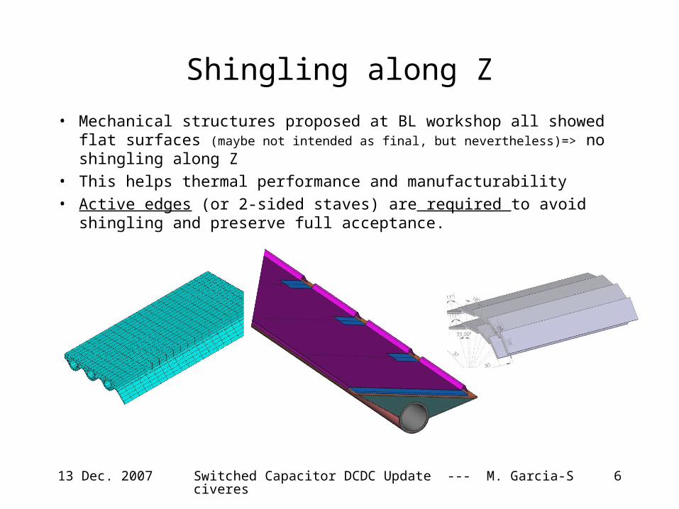
13 Dec. 2007 Switched Capacitor DCDC Update --- M. Garcia-Sciveres 6
Shingling along Z
• Mechanical structures proposed at BL workshop all showed flat surfaces (maybe not intended as final, but nevertheless)=> no shingling along Z
• This helps thermal performance and manufacturability
• Active edges (or 2-sided staves) are required to avoid shingling and preserve full acceptance.

13 Dec. 2007 Switched Capacitor DCDC Update --- M. Garcia-Sciveres 7
Assembly flow simplificationWafer probe
Bump deposition,Thin and dice
Chip probe/select
16-to-1 Flip chip
Bare module probe
Module assembly
Module full test
Stave/sector test
Stave/sector assembly
rework
NOWSIMPLER
wafer probe
1-to-1 flip-chip
SC module full probe
Stave/sector assembly
Stave/sector test
Higher level of integration at IC stage: no separate “module control chip”
More standard and higher yield 1 to 1 bump bonding: no need for ultra high KGD yield.
Bump deposition,Thin and dice
Toss bad ones

13 Dec. 2007 Switched Capacitor DCDC Update --- M. Garcia-Sciveres 8
Outer layers
• 3-D sensors and therefore active edges apply naturally to B-Layer
• But many advantages of active edges are more important for outer layers, where cost is critical:– Cost savings from using single chip modules and no shingling– Simplified assembly flow (faster and cheaper)
• Integrated stave using SC modules is therefore a good model for entire detector– Readout modularity needs to be studied for outer layers.
• Full development of active edges even for planar sensors in important for pixel upgrade!

13 Dec. 2007 Switched Capacitor DCDC Update --- M. Garcia-Sciveres 9
The integrated stave conceptual parts(examples can be replaced by equivalent function)
Signal cable with 24 flaps before lamination. Could also be multiple cables.
End of stave card could be built-inStave controller chip goes here
Al power planes added to signal cable. May contain DC-DC converters at a few points, or serial power taps.
Mechanical support with cooling.
Combine all the above and test. Then add SC modules.
Tab wraps around and is w-bonded to SC module
13 Dec. 2007 Switched Capacitor DCDC Update --- M. Garcia-Sciveres 10
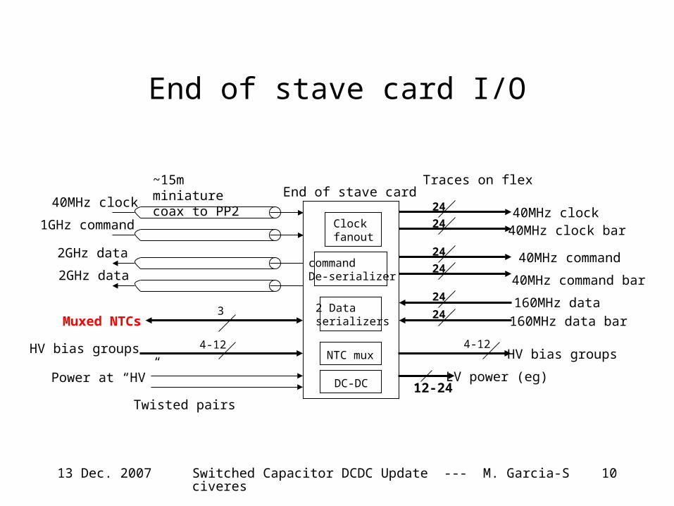
End of stave card I/O
24
24
24
24
24
24
40MHz clock 40MHz clock bar
40MHz command
40MHz command bar
160MHz data
160MHz data bar
Clock fanout
End of stave cardTraces on flex~15m miniature
coax to PP2 40MHz clock
1GHz command
2GHz data
2GHz data
LV power (eg)
command De-serializer
2 Data serializers
Power at “HV”12-24DC-DC
4-12HV bias groups 4-12HV bias groups
3Muxed NTCs
Twisted pairs
NTC mux
13 Dec. 2007 Switched Capacitor DCDC Update --- M. Garcia-Sciveres 11
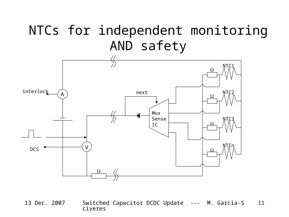
NTCs for independent monitoring AND safety
Ainterlock
VDCS
next
MuxSenseIC
NTC1
NTC2
NTC3
NTCn
13 Dec. 2007 Switched Capacitor DCDC Update --- M. Garcia-Sciveres 12
Material savings
• Items no longer used:– Module control chip– Module pigtail connectors– Shingled carbon surface
• Lighter items– Power conductors
• Less massive if SP or DC-DC• Or could tolerate larger Vdrop if DCDC placed at ends of stave.
– Mechanical structure• See mechanics pixel talk Thu. New developments not central to integrated stave
• New items needed– DC-DC (unless placed only at ends) or SP signal level shifters & control.
• Want even more reductions?– See monolithic structures tomorrow.

13 Dec. 2007 Switched Capacitor DCDC Update --- M. Garcia-Sciveres 13
Conclusion
• Many ideas, but prototyping is needed to understand details.
• Good start on mechanical items (see tomorrow)
• Not much done on passive electrical components.