128Kx16 SRAM/EEPROM MODULE€¦ · Mercury Corp. - Memory and Storage Solutions • (602) 437-1520...
16
1 Mercury Corp. - Memory and Storage Solutions • (602) 437-1520 • www.mrcy.com 4370.07E-0816-ss-WSE128K16-XXX 128Kx16 SRAM/EEPROM MODULE WSE128K16-XXX SD8 SD9 SD10 A13 A14 A15 A16 NC SD0 SD1 SD2 11 22 33 44 55 66 1 12 23 34 45 56 ED8 ED9 ED10 A6 A7 NC A8 A9 ED0 ED1 ED2 SD15 SD14 SD13 SD12 OE# NC SWE#1 SD7 SD6 SD5 SD4 SWE2# SCS2# GND SD11 A10 A11 A12 VCC SCS1# NC SD3 ED15 ED14 ED13 ED12 A0 A1 A2 ED7 ED6 ED5 ED5 VCC ECS2# EWE2# ED11 A3 A4 A5 EWE1# ECS1# GND ED3 FEATURES Access Times of 35ns (SRAM) and 150ns (EEPROM) Access Times of 45ns (SRAM) and 120ns (EEPROM) Packaging • 66 pin, PGA Type, 1.075" square HIP, Hermetic Ceramic HIP (H1) (Package 400) • 68 lead, Hermetic CQFP (G2T), 22mm (0.880") square (Package 509). Designed to fit JEDEC 68 lead 0.990" CQFJ footprint (FIGURE 2) 128Kx16 SRAM 128Kx16 EEPROM Organized as 128Kx16 of SRAM and 128Kx16 of EEPROM Memory with separate Data Buses Both blocks of memory are User Configurable as 256Kx8 Low Power CMOS Commercial, Industrial and Military Temperature Ranges TTL Compatible Inputs and Outputs Built-in Decoupling Caps and Multiple Ground Pins for Low Noise Operation Weight - 13 grams typical EEPROM MEMORY FEATURES Write Endurance 10,000 Cycles Data Retention at 25°C, 10 Years Low Power CMOS Operation Automatic Page Write Operation Page Write Cycle Time 10ms Max. Data Polling for End of Write Detection Hardware and Software Data Protection TTL Compatible Inputs and Outputs * This product is under development, is not qualified or characterized and is subject to change without notice. PIN DESCRIPTION ED0-15 EEPROM Data Inputs/Outputs SD0-15 SRAM Data Inputs/Outputs A0-16 Address Inputs SWE#1-2 SRAM Write Enable SCS#1-2 SRAM Chip Selects OE# Output Enable VCC Power Supply GND Ground NC Not Connected EWE#1-2 EEPROM Write Enable ECS#1-2 EEPROM Chip Select TOP VIEW FIGURE 1 – WSE128K16-XH1X PIN CONFIGURATION BLOCK DIAGRAM EWE1# ECS1# EWE2# ECS2# SWE2# SCS2# 128K x 8 SRAM 8 SD0-7 128K x 8 SRAM 8 SD8-15 128K x 8 EEPROM 8 ED0-7 128K x 8 EEPROM 8 ED8-15 A0-16 OE# SWE1# SCS1#
Transcript of 128Kx16 SRAM/EEPROM MODULE€¦ · Mercury Corp. - Memory and Storage Solutions • (602) 437-1520...

1Mercury Corp. - Memory and Storage Solutions • (602) 437-1520 • www.mrcy.com 4370.07E-0816-ss-WSE128K16-XXX
128Kx16 SRAM/EEPROM MODULE
WSE128K16-XXX
SD8
SD9
SD10
A13
A14
A15
A16
NC
SD0
SD1
SD2
11 22 33 44 55 66
1 12 23 34 45 56
ED8
ED9
ED10
A6
A7
NC
A8
A9
ED0
ED1
ED2
SD15
SD14
SD13
SD12
OE#
NC
SWE#1
SD7
SD6
SD5
SD4
SWE2#
SCS2#
GND
SD11
A10
A11
A12
VCC
SCS1#
NC
SD3
ED15
ED14
ED13
ED12
A0
A1
A2
ED7
ED6
ED5
ED5
VCC
ECS2#
EWE2#
ED11
A3
A4
A5
EWE1#
ECS1#
GND
ED3
FEATURES Access Times of 35ns (SRAM) and 150ns (EEPROM) Access Times of 45ns (SRAM) and 120ns (EEPROM) Packaging
• 66 pin, PGA Type, 1.075" square HIP, Hermetic Ceramic HIP (H1) (Package 400)
• 68 lead, Hermetic CQFP (G2T), 22mm (0.880") square (Package 509). Designed to fi t JEDEC 68 lead 0.990" CQFJ footprint (FIGURE 2)
128Kx16 SRAM 128Kx16 EEPROM Organized as 128Kx16 of SRAM and 128Kx16 of EEPROM
Memory with separate Data Buses Both blocks of memory are User Confi gurable as 256Kx8 Low Power CMOS Commercial, Industrial and Military Temperature Ranges TTL Compatible Inputs and Outputs Built-in Decoupling Caps and Multiple Ground Pins for Low
Noise Operation Weight - 13 grams typical
EEPROM MEMORY FEATURES Write Endurance 10,000 Cycles Data Retention at 25°C, 10 Years Low Power CMOS Operation Automatic Page Write Operation Page Write Cycle Time 10ms Max. Data Polling for End of Write Detection Hardware and Software Data Protection TTL Compatible Inputs and Outputs
* This product is under development, is not qualifi ed or characterized and is subject to change without notice.
PIN DESCRIPTIONED0-15 EEPROM Data Inputs/OutputsSD0-15 SRAM Data Inputs/OutputsA0-16 Address Inputs
SWE#1-2 SRAM Write EnableSCS#1-2 SRAM Chip Selects
OE# Output EnableVCC Power SupplyGND GroundNC Not Connected
EWE#1-2 EEPROM Write EnableECS#1-2 EEPROM Chip Select
TOP VIEW
FIGURE 1 – WSE128K16-XH1X PIN CONFIGURATION
BLOCK DIAGRAMEWE1# ECS1# EWE2# ECS2# SWE2# SCS2#
128K x 8 SRAM
8
SD0-7
128K x 8 SRAM
8
SD8-15
128K x 8 EEPROM
8
ED0-7
128K x 8 EEPROM
8
ED8-15
A0-16
OE# SWE1# SCS1#

WSE128K16-XXX
2Mercury Corp. - Memory and Storage Solutions • (602) 437-1520 • www.mrcy.com 4370.07E-0816-ss-WSE128K16-XXX
1011121314151617181920212223242526
6059585756555453525150494847464544
9 8 7 6 5 4 3 2 1 68 67 66 65 64 63 62 61
27 28 29 30 31 32 33 34 35 36 37 38 39 40 41 42 43
SD0
SD1
SD2
SD3
SD4
SD5
SD6
SD7
GNDSD8
SD9
SD10
SD11
SD12
SD13
SD14
SD15
VC
C
A11
A12
A13
A14
A15
A16
SC
S1#
OE
#S
CS
2# NC
SW
E2#
EW
E1#
EW
E2# NC
NC
NC
ED0
ED1
ED2
ED3
ED4
ED5
ED6
ED7
GNDED8
ED9
ED10
ED11
ED12
ED13
ED14
ED15
NC
A0
A1
A2
A3
A4
A5
EC
S1#
GN
DE
CS
2#S
WE
1#A
6
A7
A8
A9
A10
VC
C
0.940"
TOP VIEW
FIGURE 2 – WSE128K16-XG2TX PIN CONFIGURATION
BLOCK DIAGRAM
PIN DESCRIPTIONED0-15 EEPROM Data Inputs/OutputsSD0-15 SRAM Data Inputs/OutputsA0-16 Address Inputs
SWE#1-2 SRAM Write EnableSCS#1-2 SRAM Chip Selects
OE# Output EnableVCC Power SupplyGND GroundNC Not Connected
EWE#1-2 EEPROM Write EnableECS#1-2 EEPROM Chip Select
The Microsemi 68 lead G2T CQFP fi lls the same fi t and function as the JEDEC 68 lead CQFJ or 68 PLCC. But the G2T has the TCE and lead inspection advantage of the CQFP form.
EWE1# ECS1# EWE2# ECS2# SWE2# SCS2#
128K x 8 SRAM
8
SD0-7
128K x 8 SRAM
8
SD8-15
128K x 8 EEPROM
8
ED0-7
128K x 8 EEPROM
8
ED8-15
A0-16
OE# SWE1# SCS1#

WSE128K16-XXX
3Mercury Corp. - Memory and Storage Solutions • (602) 437-1520 • www.mrcy.com 4370.07E-0816-ss-WSE128K16-XXX
RECOMMENDED OPERATING CONDITIONSParameter Symbol Min Max UnitSupply Voltage VCC 4.5 5.5 VInput High Voltage VIH 2.0 VCC + 0.3 VInput Low Voltage VIL -0.3 +0.8 VOperating Temp. (Mil.) TA -55 +125 °C
EEPROM TRUTH TABLECS# OE# WE# Mode Data I/O
H X X Standby High ZL L H Read Data OutL H L Write Data InX H X Out Disable High Z/Data OutX X H Write
InhibitX L X
SRAM TRUTH TABLESCS# OE# SWE# Mode Data I/O Power
H X X Standby High Z StandbyL L H Read Data Out ActiveL H H Read High Z ActiveL X L Write Data In Active
DC CHARACTERISTICSVCC = 5.0V, GND = 0V, -55°C ≤ TA ≤ +125°C
Parameter Symbol Conditions Min Max UnitInput Leakage Current ILI VCC = 5.5, VIN = GND to VCC 10 μAOutput Leakage Current ILO SCS# = VIH, OE# = VIH, VOUT = GND to VCC 10 μASRAM Operating Supply Current x 16 Mode ICCx16 SCS# = VIL, OE# = ECS# = VIH, f = 5MHz, VCC = 5.5 360 mAStandby Current ISB ECS# = SCS# = VIH, OE# = VIH, f = 5MHz, VCC = 5.5 31.2 mA
SRAM Output Low Voltage (35 to 45ns) VOL IOL = 8.0mA, VCC = 4.5 0.4 V(70ns) VOL IOL = 2.1mA, VCC = 4.5 0.4 V
SRAM Output High Voltage (35 to 45ns) VOH IOH = -4.0mA, VCC = 4.5 2.4 V(70ns) VOH IOH = -1mA, VCC = 4.5 2.4 V
EEPROM Operating Supply Current x 16 Mode ICC1 ECS# = VIL, OE# = SCS# = VIH 155 mAEEPROM Output Low Voltage VOL IOL = 2.1 mA, VCC = 4.5V 0.45 VEEPROM Output High Voltage VOH1 IOH = 400 μA, VCC = 4.5V 2.4 V
NOTES:1. The ICC current listed includes both the DC operating current and the frequency dependent component (@ 5 MHz).
The frequency component typically is less than 2 mA/MHz, with OE at VIH.2. DC test conditions: VIL = 0.3V, VIH = VCC - 0.3V
ABSOLUTE MAXIMUM RATINGSParameter Symbol Min Max UnitOperating Temperature TA -55 +125 °CStorage Temperature TSTG -65 +150 °CSignal Voltage Relative to GND VG -0.5 VCC+0.5 VJunction Temperature TJ 150 °CSupply Voltage VCC -0.5 7.0 V
CAPACITANCETA = +25°C
Parameter Symbol Conditions Max UnitOE# capacitance COE VIN = 0 V, f = 1.0 MHz 50 pFWE#1-4 capacitanceHIP (PGA) CWE VIN = 0 V, f = 1.0 MHz
20pF
CQFP G2T 20CS#1-4 capacitance CCS VIN = 0 V, f = 1.0 MHz 20 pFData I/O capacitance CI/O VI/O = 0 V, f = 1.0 MHz 20 pFAddress input capacitance CAD VIN = 0 V, f = 1.0 MHz 50 pF
This parameter is guaranteed by design but not tested.

WSE128K16-XXX
4Mercury Corp. - Memory and Storage Solutions • (602) 437-1520 • www.mrcy.com 4370.07E-0816-ss-WSE128K16-XXX
FIGURE 3 – AC TEST CIRCUIT AC TEST CONDITIONSParameter Typ Unit
Input Pulse Levels VIL = 0, VIH = 3.0 VInput Rise and Fall 5 nsInput and Output Reference Level 1.5 VOutput Timing Reference Level 1.5 V
NOTES:VZ is programmable from -2V to +7V.IOL & IOH programmable from 0 to 16mA.Tester Impedance Z0 = 75 Ω.VZ is typically the midpoint of VOH and VOL.IOL & IOH are adjusted to simulate a typical resistive load circuit.ATE tester includes jig capacitance.
SRAM AC CHARACTERISTICSVCC = 5.0V, GND = 0V, -55°C ≤ TA ≤ +125°C
ParameterRead Cycle Symbol
-35 -45Units
Min Max Min MaxRead Cycle Time tRC 35 45 nsAddress Access Time tAA 35 45 nsOutput Hold from Address Change tOH 0 0 nsChip Select Access Time tACS 35 45 nsOutput Enable to Output Valid tOE 20 25 nsChip Select to Output in Low Z tCLZ1 3 3 nsOutput Enable to Output in Low Z tOLZ1 0 0 nsChip Disable to Output in High Z tCHZ1 20 20 nsOutput Disable to Output in High Z tOHZ1 20 20 ns
1. This parameter is guaranteed by design but not tested.
SRAM AC CHARACTERISTICSVCC = 5.0V, GND = 0V, -55°C ≤ TA ≤ +125°C
ParameterWrite Cycle Symbol
-35 -45Units
Min Max Min MaxWrite Cycle Time tWC 35 45 nsChip Select to End of Write tCW 25 30 nsAddress Valid to End of Write tAW 25 30 nsData Valid to End of Write tDW 20 25 nsWrite Pulse Width tWP 25 30 nsAddress Setup Time tAS 0 0 nsAddress Hold Time tAH 0 0 nsOutput Active from End of Write tOW1 4 4 nsWrite Enable to Output in High Z tWHZ1 20 25 nsData Hold Time tDH 0 0 ns
1. This parameter is guaranteed by design but not tested.
I
Current Source
D.U.T.
C = 50 pf eff
I OL
V ≈ 1.5V (Bipolar Supply)
Z
Current Source OH

5Mercury Corp. - Memory and Storage Solutions • (602) 437-1520 • www.mrcy.com 4370.07E-0816-ss-WSE128K16-XXX
WSE128K16-XXX
FIGURE 4 – SRAM READ CYCLES
ADDRESS
SRAM DATA I/O PREVIOUS DATA VALID DATA VALID
tRC
tAA
READ CYCLE 1, (SCS# = OE# = VIL, SWE# = VIH)
tOH
ADDRESS
SCS#
SOE#
SRAM DATA I/O
tRC
tAA
tACS
tCLZ
tOE
tOLZ
tCHZ
tOHZ
HIGH IMPEDANCE
READ CYCEL 2, (SWE# = VIH)
DATA VALID
FIGURE 5 – SRAM WRITE CYCLE SWE# CONTROLLED
ADDRESS
SCS#
SWE#
SRAM DATA I/O
tWC
tAW tCW
tAH
tWP
tOW
tAS
tWHZ tDW tDH
DATA VALID
WRITE CYCLE 1, SWE# CONTROLLED
FIGURE 6 – SRAM WRITE CYCEL SCS# CONTROLLED
ADDRESS
SCS#
SWE#
SRAM
DATA I/O
tWC
tAW
tCW tAS tAH
tDH tDW
tWP
DATA VALID
WRITE CYCLE 2, SCS# CONTROLLED
WSE128K16-XXX
6Mercury Corp. - Memory and Storage Solutions • (602) 437-1520 • www.mrcy.com 4370.07E-0816-ss-WSE128K16-XXX
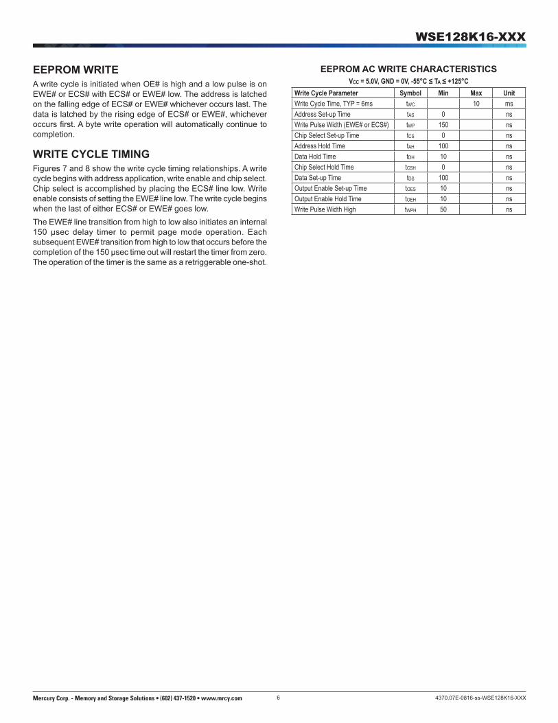
EEPROM WRITEA write cycle is initiated when OE# is high and a low pulse is on EWE# or ECS# with ECS# or EWE# low. The address is latched on the falling edge of ECS# or EWE# whichever occurs last. The data is latched by the rising edge of ECS# or EWE#, whichever occurs fi rst. A byte write operation will automatically continue to completion.
WRITE CYCLE TIMINGFigures 7 and 8 show the write cycle timing relationships. A write cycle begins with address application, write enable and chip select. Chip select is accomplished by placing the ECS# line low. Write enable consists of setting the EWE# line low. The write cycle begins when the last of either ECS# or EWE# goes low.The EWE# line transition from high to low also initiates an internal 150 μsec delay timer to permit page mode operation. Each subsequent EWE# transition from high to low that occurs before the completion of the 150 μsec time out will restart the timer from zero. The operation of the timer is the same as a retriggerable one-shot.
EEPROM AC WRITE CHARACTERISTICSVCC = 5.0V, GND = 0V, -55°C ≤ TA ≤ +125°C
Write Cycle Parameter Symbol Min Max UnitWrite Cycle Time, TYP = 6ms tWC 10 msAddress Set-up Time tAS 0 nsWrite Pulse Width (EWE# or ECS#) tWP 150 nsChip Select Set-up Time tCS 0 nsAddress Hold Time tAH 100 nsData Hold Time tDH 10 nsChip Select Hold Time tCSH 0 nsData Set-up Time tDS 100 nsOutput Enable Set-up Time tOES 10 nsOutput Enable Hold Time tOEH 10 nsWrite Pulse Width High tWPH 50 ns

7Mercury Corp. - Memory and Storage Solutions • (602) 437-1520 • www.mrcy.com 4370.07E-0816-ss-WSE128K16-XXX
WSE128K16-XXX
FIGURE 7 – EEPROM WRITE WAVEFORMS EWE# CONTROLLED
FIGURE 8 – EEPROM WRITE WAVEFORMS ECS# CONTROLLED
tDH
tWPH tWP
tCSH
tOEH
tAH
tOES
tAS
tCS
OE#
ADDRESS
ECS#1-2
EWE#1-2
EEPROM DATA IN
tWC
tDS
tDH
tWPHtWP
tCSH
tOEH
tAH
tOES
tAS
tCS
OE#
ADDRESS
ECS#1-2
EWE#1-2
EEPROMDATA IN
tDS
tWC

WSE128K16-XXX
8Mercury Corp. - Memory and Storage Solutions • (602) 437-1520 • www.mrcy.com 4370.07E-0816-ss-WSE128K16-XXX
tOH
ADDRESS
ECS#1-2
OE#
EEPROMDATA
OUTPUT
tDFtACC
tRC
tOE
tACS
OUTPUTVALID
ADDRESS VALID
HIGH Z
FIGURE 9 – EEPROM READ WAVEFORMS
EEPROM READThe WSE128K16-XXX EEPROM stores data at the memory location determined by the address pins. When ECS# and OE# are low and EWE# is high, this data is present on the outputs. When ECS# and OE# are high, the outputs are in a high impedance state. This two line control prevents bus contention.
Note: OE# may be delayed up to tACS - tOE after the falling edge of ECS# without impact on tOE or by tACC - tOE after an address change without impact on tACC.
EEPROM AC READ CHARACTERISTICSVCC = 5.0V, GND = 0V, -55°C ≤ TA ≤ +125°C
Read Cycle Parameter Symbol-120 -150
UnitMin Max Min Max
Read Cycle Time tRC 120 150 nsAddress Access Time tACC 120 150 nsChip Select Access Time tACS 120 150 nsOutput Hold from Add. Change, OE# or ECS# tOH 0 0 nsOutput Enable to Output Valid tOE 0 50 0 55 nsChip Select or OE# to High Z Output tDF 70 70 ns

WSE128K16-XXX
9Mercury Corp. - Memory and Storage Solutions • (602) 437-1520 • www.mrcy.com 4370.07E-0816-ss-WSE128K16-XXX
EEPROM DATA POLLINGThe WSE128K16-XXX offers a data polling feature for the EEPROM which allows a faster method of writing to the device. Figure 11 shows the timing diagram for this function. During a byte or page write cycle, an attempted read of the last byte written will result in the complement of the written data on D7 (for each chip.) Once the write cycle has been completed, true data is valid on all outputs and the next cycle may begin. Data polling may begin at any time during the write cycle.
FIGURE 10 – EEPROM DATA POLLING WAVEFORMS
EEPROM DATA POLLING CHARACTERISTICSVCC = 5.0V, GND = 0V, -55°C ≤ TA ≤ +125°C
Parameter Symbol Min Max UnitData Hold Time tDH 10 nsOE# Hold Time tOEH 10 nsOE# To Output Valid tOE 55 nsWrite Recovery Time tWR 0 ns
EWE#1-2
ECS#1-2
OE#
ED7
ADDRESS
tOEH
tDH tOE
tWR
HIGH Z

WSE128K16-XXX
10Mercury Corp. - Memory and Storage Solutions • (602) 437-1520 • www.mrcy.com 4370.07E-0816-ss-WSE128K16-XXX
EEPROM PAGE WRITE OPERATIONThe WSE128K16-XXX has a page write operation that allows one to 128 bytes of data to be written into the device and consecutively loads during the internal programming period. Successive bytes may be loaded in the same manner after the fi rst data byte has been loaded. An internal timer begins a time out operation at each write cycle. If another write cycle is completed within 150μs or less, a new time out period begins. Each write cycle restarts the delay period. The write cycles can be continued as long as the interval is less than the time out period.The usual procedure is to increment the least signifi cant address lines from A0 through A6 at each write cycle. In this manner a page of up to 128 bytes can be loaded in to the EEPROM in a burst mode before beginning the relatively long interval programming cycle.After the 150μs time out is completed, the EEPROM begins an internal write cycle. During this cycle the entire page of bytes will be written at the same time. The internal programming cycle is the same regardless of the number of bytes accessed.
FIGURE 11 – EEPROM PAGE MODE WRITE WAVEFORMS
EEPROM PAGE WRITE CHARACTERISTICSVCC = 5.0V, GND = 0V, -55°C ≤ TA ≤ +125°C
Page Mode Write CharacteristicsParameter Symbol Min Max Unit
Write Cycle Time, TYP = 6ms tWC 10 msAddress Set-up Time tAS 0 nsAddress Hold Time (1) tAH 100 nsData Set-up Time tDS 100 nsData Hold Time tDH 10 nsWrite Pulse Width tWP 150 nsByte Load Cycle Time tBLC 150 μsWrite Pulse Width High tWPH 50 ns
NOTE:1. Page address must remain valid for duration of write cycle.
BYTE 0 BYTE 1 BYTE 2 BYTE 3VALIDDATA
VALIDADDRESS
tWC
tBLCtWPHtWP
BYTE 127
tDS tDH
tAS tAH
OE#
ECS#1-2
EWE#1-2
ADDRESS
EEPROM DATA

11Mercury Corp. - Memory and Storage Solutions • (602) 437-1520 • www.mrcy.com 4370.07E-0816-ss-WSE128K16-XXX
WSE128K16-XXX
LOAD DATA AATO
ADDRESS 5555
LOAD DATA 55TO
ADDRESS 2AAA
LOAD DATA A0TO
ADDRESS 5555
LOAD DATA XXTO
ANY ADDRESS(4)
LOAD LAST BYTETO
LAST ADDRESS
FIGURE 12 – EEPROM SOFTWARE DATA PROTECTION ENABLE ALGORITHM(1)
WRITES ENABLED(2)
NOTES:1. Data Format: ED7 - ED0 (Hex); Address Format: A16 - A0 (Hex).2. Write Protect state will be activated at end of write even if no other data is loaded.3. Write Protect state will be deactivated at end of write period even if no other data is loaded.4. 1 to 128 bytes of data may be loaded.
ENTER DATAPROTECT STATE

WSE128K16-XXX
12Mercury Corp. - Memory and Storage Solutions • (602) 437-1520 • www.mrcy.com 4370.07E-0816-ss-WSE128K16-XXX
EEPROM SOFTWARE DATA PROTECTIONA software write protection feature may be enabled or disabled by the user. When shipped by WEDC, the WSE128K16-XXX has the feature disabled. Write access to the device is unrestricted.To enable software write protection, the user writes three access code bytes to three special internal locations. Once write protection has been enabled, each write to the EEPROM must use the same three byte write sequence to permit writing. After setting software data protection, any attempt to write to the device without the three-byte command sequence will start the internal write timers. No data will be written to the device, however, for the duration of twc. The write protection feature can be disabled by a six byte write sequence of specifi c data to specifi c locations. Power transitions will not reset the software write protection.Each 128K byte block of the EEPROM has independent write protection. One or more blocks may be enabled and the rest disabled in any combination. The software write protection guards against inadvertent writes during power transitions, or unauthorized modifi cation using a PROM programmer.
EEPROM HARDWARE DATA PROTECTIONThese features protect against inadvertent writes to the WSE128K16-XXX. These are included to improve reliability during normal operation: a) VCC power on delay
As VCC climbs past 3.8V typical the device will wait 5 msec typical before allowing write cycles.
b) VCC senseWhile below 3.8V typical write cycles are inhibited.
c) Write inhibitingHolding OE# low and either ECS# or EWE# high inhibits write cycles.
d) Noise fi lterPulses of <8ns (typ) on EWE# or ECS# will not initiate a write cycle.
FIGURE 13 – EEPROM SOFTWARE DATA PROTECTION DISABLE ALGORITHM(1)
EXIT DATA(3)
PROTECT STATE
NOTES:1. Data Format: ED7 - ED0 (Hex);
Address Format: A16 - A0 (Hex).2. Write Protect state will be activated at end of write even if no other data
is loaded.3. Write Protect state will be deactivated at end of write period even if no
other data is loaded.4. 1 to 128 bytes of data may be loaded.
LOAD DATA AATO
ADDRESS 5555
LOAD DATA 55TO
ADDRESS 2AAA
LOAD DATA 80TO
ADDRESS 5555
LOAD DATA AATO
ADDRESS 5555
LOAD DATA 55TO
ADDRESS 2AAA
LOAD DATA 20TO
ADDRESS 5555
LOAD DATA XXTO
ANY ADDRESS(4)
LOAD LAST BYTETO
LAST ADDRESS

13Mercury Corp. - Memory and Storage Solutions • (602) 437-1520 • www.mrcy.com 4370.07E-0816-ss-WSE128K16-XXX
WSE128K16-XXX
PIN 1 IDENTIFIER SQUARE PAD ON BOTTOM
27.3 (1.075) ± 0.25 (0.010) SQ
3.81 (0.150) ± 0.13 (0.005) 1.42 (0.056) ± 0.13 (0.005)
0.76 (0.030) ± 0.13 (0.005)
1.27 (0.050) ± TYP DIA
25.4 (1.0) TYP
0.46 (0.018) ± 0.05 (0.002) DIA
4.34 (0.171) MAX
2.54 (0.100) TYP 15.24 (0.600) TYP
25.4 (1.0) TYP
PACKAGE 400 – 66 PIN, PGA TYPE, CERAMIC HEX-IN-LINE PACKAGE, HIP (H1)
ALL LINEAR DIMENSIONS ARE MILLIMETERS AND PARENTHETICALLY IN INCHES

14Mercury Corp. - Memory and Storage Solutions • (602) 437-1520 • www.mrcy.com 4370.07E-0816-ss-WSE128K16-XXX
WSE128K16-XXX
0.38 (0.015) ± 0.05 (0.002)
0.27 (0.011) ± 0.04 (0.002)
25.15 (0.990) ± 0.26 (0.010) SQ
1.27 (0.050) TYP
24.03 (0.946) ± 0.26 (0.010)
22.36 (0.880) ± 0.26 (0.010) SQ
20.3 (0.800) REF
4.57 (0.180) MAX
0.19 (0.007) ± 0.06 (0.002)
23.87 (0.940) REF
1.0 (0.040) ± 0.127 (0.005)
0.25 (0.010) REF
1° / 7°
R 0.25 (0.010)
DETAIL A
SEE DETAIL "A"
Pin 1
0.940" TYP
PACKAGE 509 – 68 LEAD, CERAMIC QUAD FLAT PACK, CQFP (G2T)
The WEDC 68 lead G2T CQFP fi lls the same fi t and function as the JEDEC 68 lead CQFJ or 68 PLCC. But the G2T has the TCE and lead inspection advantage of the CQFP form.
ALL LINEAR DIMENSIONS ARE MILLIMETERS AND PARENTHETICALLY IN INCHES

15Mercury Corp. - Memory and Storage Solutions • (602) 437-1520 • www.mrcy.com 4370.07E-0816-ss-WSE128K16-XXX
WSE128K16-XXX
ORDERING INFORMATION
MERCURY SYSTEMS
SRAM
EEPROM
ORGANIZATION, 128K x 16
ACCESS TIME (ns)35 = 35ns SRAM and 150ns EEPROM42 = 45ns SRAM and 120ns EEPROM
PACKAGE TYPE:H1 = 1.075" sq. Ceramic Hex-In-line Package, HIP (Package 400)G2T = 22.4mm Ceramic Quad Flat Pack, CQFP (Package 509)
DEVICE GRADE:M = Military Screened -55°C to +125°C I = Industrial -40°C to +85°CC = Commercial 0°C to +70°C
LEAD FINISH:Blank = Gold plated leadsA = Solder dip leads
W S E 128K16 - XXX X X X

16Mercury Corp. - Memory and Storage Solutions • (602) 437-1520 • www.mrcy.com
Mercury Systems reserves the right to change products or specifi cations without notice.© 2016 Mercury Systems. All rights reserved.
4370.07E-0816-ss-WSE128K16-XXX
WSE128K16-XXX
Document Title128Kx16 SRAM/EEPROM MODULE
Revision History
Rev # History Release Date StatusRev 4 Changes (Pg. 1-16)
4.1 Change document layout from White Electronic Designs to Microsemi4.2 Add document Revision History page
August 2011 Final
Rev 5 Changes (Pg. 1, 4, 8)5.1 Remove all references to 70ns (SRAM) and 300ns (EEPROM)s
March 2012 Final
Rev 6 Changes (Pg. All) (ECN 10156)6.1 Change document layout from Microsemi to Mercury Systems
August 2016 Final
Rev 7 Changes (Pg. All) (ECN 10957)7.1 Update data sheet with new Mercury logo
October 2018 Final