
1/2.7” 1080p 3.0µm BSI CMOS Image Sensor
29
FSRJ2395 1/2.7” 1080p 3.0μm BSI CMOS Image Sensor 1 Preliminary Datasheet Rev 2.0 Confidential and Proprietary Foxconn reserves the right to change product or specifications without notice © 2018 Foxconn. All rights reserved General Description: The FSRJ2395 camera chip is a FOXCONN System Corporation product and qualified by Foxconn. The FSRJ2395 is sophisticatedly integrated with a 1080p BSI CMOS image sensor of 1/2.7-inch optical format and an on-chip ISP (Image Signal Processor) that features auto black level calibration and bad pixel correction. The FSRJ2395 has two MIPI CSI-2 compliance serial interfaces: TX (up to 2 data lanes) and RX (1 data lane). It consists of a 1936 x 1096 active pixel sensor (APS) array that’s capable of operating at 1080p 60 frames per second (FPS) and 1080p HDR 30 frames per second. In addition to featuring superior low-light sensitivity and low dark current performance, a better and clear image is achieved through significant reduction of fixed pattern noise through an on-chip 10-bit ADC, programmable gain control (PGA) and correlated double sampling (CDS). The FSRJ2395 also includes a 32- kbit one-time programmable (OTP) memory. All ISP functions and sensor operations can be controlled and accessed by host via a 2-wire serial bus interface. The FSRJ2395 camera chip is suitable for security and surveillance applications as well as low profile camera module packaging which is available in CSP packaging. Features: Automatic Controls: Automatic Black Level (ABLC) Image Quality Controls: Bad Pixel Correction Programmable Controls: 2-exposure HDR mode Frame rate and frame size Binning Mode Manual AEC/AGC/AWB Control Two Wire I 2 C Control with Programmable Column and row sub-sampling Mirror, flip, windowing and cropping Multiple camera frame sync Embedded Data Line On-chip temperature sensor 32K-Bit one-time programmable memory (OTP) MIPI data type/virtual channel support MIPI: 2 lane TX and 1 lane RX (upto 800Mbps/Lane) Output formats and Interfaces: 10-bit raw MIPI CSI-2 1-lane or 2-lane Other controls: Register group access capability Key Specifications: Optical Format 1/2.7-inch. Active Pixel Array (1080P) 1936H x 1096V Pixel Size 3.0 μm x 3.0 μm Color Filter Array RGB Bayer Pattern Chief Ray Angle 9 ° Linear Shutter Type Electronic Rolling Shutter Maximum Frame Rate 1080P : 60fps 1080P HDR: 30fps Power Supply AVDD 3.0 – 3.6V (3.3V nominal) I/O 1.7 – AVDD DVDD 1.2V Power Consumption Active <150mW Standby <7μW Output Formats 10-bit RAW Operating Temperature -30ºC to 85ºC Storage Temperature -40ºC to 95ºC Package Dimensions (μm2) 6,790x 4,890 Functional Block Image Sensor Array Serial Interface MIPI TX PLL System and Timing Control ADC SCP SCN SDP[1:0] SDN[1:0] ICLK IDAT RCK RSTB MIPI RX RCP RDP RCN RDN ISP Pipeline PINSEL FS STROBE Ordering Information: Part Number Description FSRJ2395-XXX CSP
Transcript of 1/2.7” 1080p 3.0µm BSI CMOS Image Sensor

FSRJ2395 1/2.7” 1080p 3.0µm BSI CMOS Image Sensor
1 Preliminary Datasheet Rev 2.0 Confidential and Proprietary Foxconn reserves the right to change product or specifications without notice
© 2018 Foxconn. All rights reserved
General Description: The FSRJ2395 camera chip is a FOXCONN System Corporation product and qualified by Foxconn. The FSRJ2395 is sophisticatedly integrated with a 1080p BSI CMOS image sensor of 1/2.7-inch optical format and an on-chip ISP (Image Signal Processor) that features auto black level calibration and bad pixel correction.
The FSRJ2395 has two MIPI CSI-2 compliance serial interfaces: TX (up to 2 data lanes) and RX (1 data lane). It consists of a 1936 x 1096 active pixel sensor (APS) array that’s capable of operating at 1080p 60 frames per second (FPS) and 1080p HDR 30 frames per second. In addition to featuring superior low-light sensitivity and low dark current performance, a better and clear image is achieved through significant reduction of fixed pattern noise through an on-chip 10-bit ADC, programmable gain control (PGA) and correlated double sampling (CDS). The FSRJ2395 also includes a 32-kbit one-time programmable (OTP) memory.
All ISP functions and sensor operations can be controlled and accessed by host via a 2-wire serial bus interface.
The FSRJ2395 camera chip is suitable for security and surveillance applications as well as low profile camera module packaging which is available in CSP packaging.
Features:
Automatic Controls: Automatic Black Level (ABLC)
Image Quality Controls: Bad Pixel Correction
Programmable Controls: 2-exposure HDR mode Frame rate and frame size Binning Mode Manual AEC/AGC/AWB Control Two Wire I2C Control with Programmable Column and row sub-sampling Mirror, flip, windowing and cropping Multiple camera frame sync Embedded Data Line On-chip temperature sensor 32K-Bit one-time programmable memory (OTP) MIPI data type/virtual channel support MIPI: 2 lane TX and 1 lane RX (upto 800Mbps/Lane)
Output formats and Interfaces: 10-bit raw MIPI CSI-2 1-lane or 2-lane
Other controls: Register group access capability
Key Specifications:
Optical Format 1/2.7-inch.
Active Pixel Array (1080P) 1936H x 1096V
Pixel Size 3.0 µm x 3.0 µm
Color Filter Array RGB Bayer Pattern
Chief Ray Angle 9 ° Linear
Shutter Type Electronic Rolling Shutter
Maximum Frame Rate 1080P : 60fps 1080P HDR: 30fps
Power Supply
AVDD 3.0 – 3.6V (3.3V nominal)
I/O 1.7 – AVDD
DVDD 1.2V
Power Consumption
Active <150mW
Standby <7µW
Output Formats 10-bit RAW
Operating Temperature -30ºC to 85ºC
Storage Temperature -40ºC to 95ºC
Package Dimensions (µm2) 6,790x 4,890
Functional Block
Image Sensor Array
Serial Interface
MIPITX
PLLSystem
and Timing Control
ADCSCPSCNSDP[1:0]SDN[1:0]
ICLK
IDAT
RCK
RSTB
MIPIRX
RCP
RDPRCN
RDN
ISP Pipeline
PINSEL
FS
STROBE
Ordering Information:
Part Number Description FSRJ2395-XXX CSP

FSRJ2395 1/2.7” 1080p 3.0µm BSI CMOS Image Sensor
2 Preliminary Datasheet Rev 2.0 Confidential and Proprietary Foxconn reserves the right to change product or specifications without notice
© 2018 Foxconn. All rights reserved
Table of Contents
Contents General Description: .............................................................................................................................................................................. 1
Features: ............................................................................................................................................................................................... 1
Key Specifications: ................................................................................................................................................................................ 1
Functional Block .................................................................................................................................................................................... 1
Ordering Information: ............................................................................................................................................................................ 1
Table of Contents ................................................................................................................................................................................. 2
List of Figures ........................................................................................................................................................................................ 3
List of Table ........................................................................................................................................................................................... 3
1. Signal Descriptions ..................................................................................................................................................................... 4
2. System Level Description ........................................................................................................................................................... 7
2.1 Functional Overview ................................................................................................................................................................... 7
2.2 Pixel Array Format ...................................................................................................................................................................... 7
2.3 System Clock and PLL Control ................................................................................................................................................... 9
2.4 Two Wire Serial Peripheral Interface ........................................................................................................................................ 10
2.5 Group Access Function ............................................................................................................................................................ 12
2.6 Power Up and Power Down Sequence .................................................................................................................................... 12
2.7 Power State Transition ............................................................................................................................................................. 14
3. Manual Exposure Control ......................................................................................................................................................... 15
4. ISP Test Pattern ....................................................................................................................................................................... 16
5. MIPI Interface ........................................................................................................................................................................... 16
6. Electrical Characteristics (TBD)................................................................................................................................................ 17
7. Register Descriptions ............................................................................................................................................................... 18
8. Optical Specifications ............................................................................................................................................................... 26
8.1 Lens Chief Ray Angle ............................................................................................................................................................... 26
9. Mechanical Specifications ........................................................................................................................................................ 27
9.1 Physical Specifications ............................................................................................................................................................. 27
Revision History .................................................................................................................................................................................. 29

FSRJ2395 1/2.7” 1080p 3.0µm BSI CMOS Image Sensor
3 Preliminary Datasheet Rev 2.0 Confidential and Proprietary Foxconn reserves the right to change product or specifications without notice
© 2018 Foxconn. All rights reserved
List of Figures Figure 1 CSP Top View Pin Diagram ............................................................................................................................................................. 6
Figure 2 Functional Block Diagram ................................................................................................................................................................ 7
Figure 3 Pixel Array Structure ........................................................................................................................................................................ 8
Figure 4 Pixel Array Matrix - Read Out Direction ............................................................................................................................................ 8
Figure 5 PLL1 (Analog/System) Clock Tree ................................................................................................................................................... 9
Figure 6 PLL2 (MIPI TX) Clock Tree .............................................................................................................................................................. 9
Figure 7 Two Wire IDAT/ICLK Serial Interface Timing Definition ................................................................................................................. 10
Figure 8 Power Up and Power Down Sequence .......................................................................................................................................... 13
Figure 9 Power State Transition ................................................................................................................................................................... 14
Figure 10 Color Bar ...................................................................................................................................................................................... 16
Figure 11 Chief Ray Angle ........................................................................................................................................................................... 26
Figure 12 CSP Top, Bottom and Side View.................................................................................................................................................. 27
List of Table
Table 1 FSRJ2395 CSP Package Table ........................................................................................................................................................ 4
Table 2 PLL Control Registers ....................................................................................................................................................................... 9
Table 3 Timing Characteristics of IDAT and ICLK lines ................................................................................................................................ 10
Table 4 Power Up and Power Down Sequence Timing ................................................................................................................................ 13
Table 5 Exposure Control ............................................................................................................................................................................. 15
Table 6 Color Bar Test Pattern ..................................................................................................................................................................... 16
Table 7 Absolute Maximum Ratings (voltages referenced to ground) .......................................................................................................... 17
Table 8 DC Characteristics (-20°C <TA<70 C), voltages referenced to ground ........................................................................................... 17
Table 9 CSP Package Dimensions .............................................................................................................................................................. 28

FSRJ2395 1/2.7” 1080p 3.0µm BSI CMOS Image Sensor
4 Preliminary Datasheet Rev 2.0 Confidential and Proprietary Foxconn reserves the right to change product or specifications without notice
© 2018 Foxconn. All rights reserved
1. Signal Descriptions
Table 1 shows a list of PIN names, types and signal descriptions for the FSRJ2395 CSP packaged image sensor.
Table 1 FSRJ2395 CSP Package Table
Pin No Pin Name Pin Type Pin Description Voltage
A1 AVD2 Power Analog circuit power 3.3v(2.7~3.6v)
A2 VR0 Reference Analog internal reference -
A3 RSTB Input System shutdown/reset, active low with internal pull down resistor -
A4 DVDD1 Power Digital circuit power 1.2v(1.08~1.32v)
A5 AVDD Power Analog circuit power 3.3v(2.7~3.6v)
A6 STR IO Strobe -
A7 FS IO System sync -
A8 IOVDD Power IO circuit power 3.3v(1.7~3.6v)
A9 DVDD1 Power Digital circuit power 1.2v(1.08~1.32v)
A10 AVDD Power Analog circuit power 3.3v(2.7~3.6v)
B1 VR3 Reference Analog internal reference -
B2 AGND Ground Analog circuit ground 0v
B3 VTST Output Test Pin -
B4 IOGND Ground IO circuit ground 0v
B5 PINSEL Input ID selection -
B6 IOVDD Power IO circuit power 3.3v(1.7~3.6v)
B7 DVDD1 Power Digital circuit power 1.2v(1.08~1.32v)
B8 AGND Ground Analog circuit ground 0v
B9 IOGND Ground IO circuit ground 0v
B10 AVD2 Power Analog circuit power 3.3v(2.7~3.6v)
C1 AVDD Power Analog circuit power 3.3v(2.7~3.6v)
C10 AGND Ground Analog circuit ground 0v
D1 AGND Ground Analog circuit ground 0v
D2 RDP IO MIPI RX data lane positive input -

FSRJ2395 1/2.7” 1080p 3.0µm BSI CMOS Image Sensor
5 Preliminary Datasheet Rev 2.0 Confidential and Proprietary Foxconn reserves the right to change product or specifications without notice
© 2018 Foxconn. All rights reserved
Pin No Pin Name Pin Type Pin Description Voltage
D3 RDN IO MIPI RX data lane negative input -
D4 AVDD Power Analog circuit power 3.3v(2.7~3.6v)
D5 DVDD2 Power Digital circuit power 1.2v(1.08~1.32v)
D6 IOGND Ground IO circuit ground 0v
D7 IOGND Ground IO circuit ground 0v
D10 AGND Ground Analog circuit ground 0v
E1 RCK Input System input reference clock -
E2 DVDD2 Power Digital circuit power 1.2v(1.08~1.32v)
E3 AGND Ground Analog circuit ground 0v
E4 RCP IO MIPI RX clock lane positive input -
E5 SDN1 IO MIPI data lane negative output -
E6 SCN IO MIPI clock lane negative output -
E7 SDN0 IO MIPI data lane negative output -
E8 IOGND Ground IO circuit ground 0v
E9 IDAT IO I2C data -
E10 DVDD2 Power Digital circuit power 1.2v(1.08~1.32v)
F1 AVDD Power Analog circuit power 3.3v(2.7~3.6v)
F2 IOGND Ground IO circuit ground 0v
F4 RCN IO MIPI RX clock lane negative input -
F5 SDP1 IO MIPI data lane positive output -
F6 SCP IO MIPI clock lane positive output -
F7 SDP0 IO MIPI data lane positive output -
F8 DVDD2 Power Digital circuit power 1.2v(1.08~1.32v)
F9 ICLK Input I2C clock -
F10 IOGND Ground IO circuit ground 0v

FSRJ2395 1/2.7” 1080p 3.0µm BSI CMOS Image Sensor
6 Preliminary Datasheet Rev 2.0 Confidential and Proprietary Foxconn reserves the right to change product or specifications without notice
© 2018 Foxconn. All rights reserved
Figure 1 CSP Top View Pin Diagram
VR0 RSTB AVDD STR DVDD1 AVDD
A1 A2 A3 A5 A6 A7
AVD2
A9 A10
AGND VTST PINSEL IOVDD DVDD1 IOGND AVD2
B1 B2 B4B3 B5 B6 B7 B8
VR3
B9 B10
C1
AVDD
C10
IOGND SDP1 SCP SDP0 ICLK IOGND
F1 F2 F4 F5 F6 F7 F8
AVDD
F9 F10
IOGND AGND
RCN DVDD2
DVDD2 AGND SDN1 SCN SDN0 IDAT DVDD2
E1 E2 E4E3 E5 E6 E7 E8
RCK
E9 E10
RDP RDN DVDD2 IOGND IOGND AGND
D1 D2 D4D3 D5 D6 D7
AGND
D10
A4 A8
DVDD1 IOVDDFS
AGND
AVDD
RCP IOGND

FSRJ2395 1/2.7” 1080p 3.0µm BSI CMOS Image Sensor
7 Preliminary Datasheet Rev 2.0 Confidential and Proprietary Foxconn reserves the right to change product or specifications without notice
© 2018 Foxconn. All rights reserved
2. System Level Description
2.1 Functional Overview
The FSRJ2395 consists of a progressive-scan CMOS image sensor and an ultra-high precision on-chip phased-locked loop
(PLL) that transform a master input clock (6~27 MHz) into several internal clocks for different timing purposes. Figure 2
illustrates a functional block diagram of the FSRJ2395 camera chip.
Figure 2 Functional Block Diagram
Image Sensor Array
Serial Interface
MIPITX
PLLSystem
and Timing Control
ADCSCPSCNSDP[1:0]SDN[1:0]
ICLK
IDAT
RCK
RSTB
MIPIRX
RCP
RDPRCN
RDN
ISP Pipeline
PINSEL
FS
STROBE
The FSRJ2395 internal registers can be programmed through a two-wire I2C compatible interface. Pixel data is collected
through the timing control circuitry based on row-wise sequential read-out from the 2MP active-pixel image sensor array. Each
read-out is followed by a reset interval during which incident light is integrated with the row pixels. Exposure control is achieved
by varying the time interval between read-out and reset. Followed by row-wises read-out, column data is sequenced through the
analog data path for analog gain to be applied and then sent to the analog signal to digital signal converter (ADC). The output of
the ADC is then processed through the digital data path where ISP functions can be applied. These functions include black level
calibration and bad pixel correction. The final processed data are then output via the MIPI CSI-2 standard interface.
2.2 Pixel Array Format
The FSRJ2395 pixel array consists of a 1936x1096 pixels matrix. Each pixel is addressable by row and column where the origin
of the coordinate (0, 0) is located at the upper left corner of the pixel array. The optical black output lines are designed for black
level calibration. The significant 1920x1080 output image array is surrounded by 8 dummy lines to each border. (See Figure 3
and Figure 4)

FSRJ2395 1/2.7” 1080p 3.0µm BSI CMOS Image Sensor
8 Preliminary Datasheet Rev 2.0 Confidential and Proprietary Foxconn reserves the right to change product or specifications without notice
© 2018 Foxconn. All rights reserved
Figure 3 Pixel Array Structure
Optical Black Lines
Output Image Array1920 x 1080
8 dummy Lines
8 dummy lines
8 d
umm
y lin
es
8 dum
my lines
(0,0)
(1935,1095)
Active Image Array
Active pixel is defined as any addressable pixel within the active image array which includes both dummy and significant pixels.
The output image array or number of significant pixels is typically 1920x1080 for 1080p.
Figure 4 Pixel Array Matrix - Read Out Direction
B
G
B
G
B
G
B
G
B
G
B
G
B
G
G
B
G B
R G
G B
R G
G B
R G
G B
R G
G B
R G
G B
R G
G B
R G
G B
R G
G B
R G
G B
R G
G B
R G
G B
R G
G B
R G
G B
R G
G B
R G
G B
R G
G B
R G
G B
R G
G B
R G
G B
R G
G B
R G
G B
R G
G B
R G
G B
R G
G B
R G
G B
R G
G B
R G
G B
R G
G B
R G
G B
R G
G B
R G
G
B
R G
G B
R G
G B
R G
G B
R G
G B
R G
G B
R G
G B
R G
G B
R G
G B
R G
G B
R G
G B
R G
G B
R G
G B
R G
G
R
G
R
G
R
G
R
Row Read O
ut (y)
(0,0)
G B
R G
G B
R G
G B
R G
G B
R G
G B
R G
G B
R G
G
R G
G B
R G
G B
R G
G B
R G
G B
R G
G B
R G
G B
R G
G B
R G
G
R G
G B
R G
G B
R G
G B
R G
G B
R G
G B
R G
G B
R G
G B
R G
G
R
G
R
B
G
R
G
RG
G B
R G
G B
G B
R G
G B
G B
R G
G B
G
G B
R G
G B
R G
G B
R G
G B
R G
G B
R G
G B
R G
G B
R G
G B
R G
G B
R G
G B
R G
G B
R G
G
R G
G B
R G
G B
R G
G
R
G
R
Column Read Out (x)
Dummy Pixels
Active Image Array
B Note that The first significant pixel starts at coordinate (y=8,x=8)
B
B
B
G
B
R R G R G
Significant Pixels

FSRJ2395 1/2.7” 1080p 3.0µm BSI CMOS Image Sensor
9 Preliminary Datasheet Rev 2.0 Confidential and Proprietary Foxconn reserves the right to change product or specifications without notice
© 2018 Foxconn. All rights reserved
2.3 System Clock and PLL Control
The FSRJ2395’s on-chip PLL allows input clock (PAD_CLK) frequency of range 6~27MHz.
Figure 5 PLL1 (Analog/System) Clock Tree
Figure 6 PLL2 (MIPI TX) Clock Tree
Table 2 PLL Control Registers
Function Register RW Description
PLL1 Divider2 0x0303 RW [3:0] pll1_div2[3:0], range=8~30. default=/8
PLL1 Divider 0x0303 RW [5:4] pll1_div[1:0], range=1,2,4,8. default=/1
PLL2 Divider 0x0304 RW [1:0] pll2_div[1:0], range=1,2,4,8. default=/8
PLL1 Post Divider 0x0304 RW [3:2] pll1_post_div[1:0], range=1,2,4,8. default=/1
PLL2 Post Divider 0x3514 RW [3:2] pll2_post_div[1:0], range=1,2,4,8. default=/2
PLL1 Pre Divider 0x0305 RW [1:0] pll1_pre_div[1:0], range=1,2,3,4. default=/3
PLL2 Pre Divider 0x3515 RW [1:0] pll2_pre_div[1:0], range=1,2,3,4. default=/3
PLL1 Loop Multiplier 0x0307 RW [7:0] pll1_loop[7:0], range=2~255. default=/132
PLL2 Loop Multiplier 0x3517 RW [7:0] pll2_loop[7:0], range=2~255. default=/165
PLL Bypass 0x3585 RW [4] bypass
PLL1 PRE DIV
/(1~4)
PLL1 LOOP MULTIPLIER
X(2~255)
PLL1 POST DIV
/(1,2,4,8) PLL1 DIV2
/(8~30) PLL1 DIV /(1,2,4,8)
SYS CLOCK LOOP INPUT
CLOCK PAD CLOCK
PLL2 PRE DIV
/(1~4)
PLL2 LOOP MULTIPLIER
X(2~255)
PLL2 POST DIV
/(1,2,4,8) PLL2 DIV /(1,2,4,8) /8
MIPI P-CLOCK LOOP INPUT
CLOCK PAD CLOCK
MIPI CLOCK

FSRJ2395 1/2.7” 1080p 3.0µm BSI CMOS Image Sensor
10 Preliminary Datasheet Rev 2.0 Confidential and Proprietary Foxconn reserves the right to change product or specifications without notice
© 2018 Foxconn. All rights reserved
2.4 Two Wire Serial Peripheral Interface
The two wire serial interface consists of a simple bi-directional bus that features a serial data line (IDAT) and a serial clock line
(ICLK). Both IDAT and ICLK are connected via a pull-up resistor. When the bus is free, both lines are HIGH. Data on the bus
can be transferred at up to 400 Kbit/s. A complete data transfer consists of a START condition, a combined 7-bit slave device
address followed by an eighth bit read or write data direction RW� , a 1-bit acknowledge (A), followed by N bytes of data + 1-bit
acknowledge (A) or negative-acknowledge (A�) and terminated with a STOP condition.
Table 3 Timing Characteristics of IDAT and ICLK lines
Symbol Description Min Max Unit
S Start condition - - -
P Stop condition - - -
ICLK Serial Clock Frequency 0 400 kHz
IDAT Serial Data - - -
Tf Fall time of both IDAT and ICLK signals - 300 ns
Tr Rise time of both IDAT and ICLK signals - 300 ns
TLow Low period of the ICLK clock 1.3 - µs
Thigh High period of the ICLK clock 0.6 - µs
Tsu Data set-up time 100 - ns
Thd Data hold time 0 0.9 µs
Tsu-sto Set-up time for STOP condition 0.6 - µs
Thd-sta Hold time for START condition 0.6 - µs
TBuf Bus free time between a STOP and START condition 1.3 - µs
Cb Capacitive Load for each bus line - 400 pF
Figure 7 Two Wire IDAT/ICLK Serial Interface Timing Definition
IDAT
ICLK
Tf
P
THigh
…...
Tr
TBuf
SS
Thd-staTsu-stoThd
TLow
Tsu

FSRJ2395 1/2.7” 1080p 3.0µm BSI CMOS Image Sensor
11 Preliminary Datasheet Rev 2.0 Confidential and Proprietary Foxconn reserves the right to change product or specifications without notice
© 2018 Foxconn. All rights reserved
….
Single Read Operation
S Device ID W A
S Device ID
Multiple Read Operation
S Device ID W A
S Device ID R A Data A Data A Data NA P
Single Write Operation
S Device ID W
Multiple Write Operation
S Device ID W
Data A …. Data A …. Data A P
S = Start Condition P = Stop Condition R = Read W = WriteHi = Address [15:8]Lo = Address [7:0]A = Acknowledge NA = Negative-acknowledge
Hi A Lo
Hi A Lo
A P
A P
A Hi A Lo A
A Hi A Lo A Data P Data A
R A Data NA P
Data P
FSRJ2395 1/2.7” 1080p 3.0µm BSI CMOS Image Sensor
12 Preliminary Datasheet Rev 2.0 Confidential and Proprietary Foxconn reserves the right to change product or specifications without notice
© 2018 Foxconn. All rights reserved
2.5 Group Access Function
The FSRJ2395 supports register group access of up to 8 groups, by programming the start address (with the exception of
group0) and length of each group at register 0x3401-0x3403 (group1 to group3’s start address), 0x3410-0x3413 (group4 to
group7’s start address) and register 0x3404-0x3407 (group1 to group3’s length), 0x3414-0x3417 (group4 to group7’s length).
Note that group0 start address is fixed at 0xe000. Register settings can be preloaded to the internal buffer first. When activated,
data are read out and written to the destination registers.
The internal buffer starts from address 0xe000 of size 768 bytes can store up to 256 register settings. Buffer is accessed byte-
wise during write operation and 3 bytes at a time during read operation. Group access is controlled by register 0x340f. In fast
write mode, register settings are read from specified group (0x340f [2:0]) from the internal buffer and immediately written to the
destination registers. In delay write mode, the write operation will start at the end of frame upon receiving the command through
register 0x340f.
Example:
6c 3401 04 ; group1 start address=0x30
6c 3405 02 ; group1 length
6c e030 3c ; r3c00=03
6c e031 00
6c e032 03
6c e033 3d ; r3d01=77
6c e034 01
6c e035 77
6c 340f 10 ; delay write group0
6c 340f 21 ; fast write group1
Note:
group1 starts at e030 (start address = 04x3x4 = 0x30 + base address) of length 2.
2.6 Power Up and Power Down Sequence
The digital IOVDD and analog AVDD supply voltages can be powered up in any order.
On Power Up:
1. RSTB pulled LOW
2. IOVDD is powered up (e.g. 1.8 V) IOVDD <= AVDD
3. AVDD is powered up (e.g. 3.3 V)
4. RSTB pulled HIGH
5. Wait for 8000 clock cycles RCK
6. Access I2C
7. Send initial settings

FSRJ2395 1/2.7” 1080p 3.0µm BSI CMOS Image Sensor
13 Preliminary Datasheet Rev 2.0 Confidential and Proprietary Foxconn reserves the right to change product or specifications without notice
© 2018 Foxconn. All rights reserved
8. Set Streaming Mode 0x0100 = 1
The digital IOVDD and analog AVDD supply voltages can be powered down in any order.
On Power Down:
1. Set Software Standby 0x0100 = 0
2. Wait for current frame to finish streaming
3. RSTB pulled LOW
4. Power down AVDD
5. Power down IOVDD
Figure 8 Power Up and Power Down Sequence
IOVDD
AVDD
RSTB
RCLK
I2C
t1
t2
t4
t5
t6
I2C Access OK
t3
Table 4 Power Up and Power Down Sequence Timing
Symbol Description Min Max Unit
t1 IOVDD to AVDD 0 - ms
t2 AVDD to RSTB 100 106 µs
t3 RSTB to RCLK 100 106 µs
t4 Clock cycles required before first I2C access 8000 - Clock Cycle
t5 RSTB to AVDD off 100 106 µs
t6 AVDD off to IOVDD off 100 106 µs

FSRJ2395 1/2.7” 1080p 3.0µm BSI CMOS Image Sensor
14 Preliminary Datasheet Rev 2.0 Confidential and Proprietary Foxconn reserves the right to change product or specifications without notice
© 2018 Foxconn. All rights reserved
2.7 Power State Transition
Figure 9 Power State Transition
Active Mode
Power off Mode
Sleep Mode Hibernate ModeIOVDD offAVDD off
IOVDD onAVDD on
IOVDD offAVDD off
IOVDD offAVDD off
Wake Up RSTB LOW
RSTB HISleep
On “Sleep”:
1. Set Software Standby 0x0100[7:0] = 0x00
2. Turn off MIPI 0x328b[7] = 0x1
On “Wake Up”:
1. Turn on MIPI 0x328b[7] = 0x0
2. Set Streaming 0x0100[7:0] = 0x01
FSRJ2395 1/2.7” 1080p 3.0µm BSI CMOS Image Sensor
15 Preliminary Datasheet Rev 2.0 Confidential and Proprietary Foxconn reserves the right to change product or specifications without notice
© 2018 Foxconn. All rights reserved
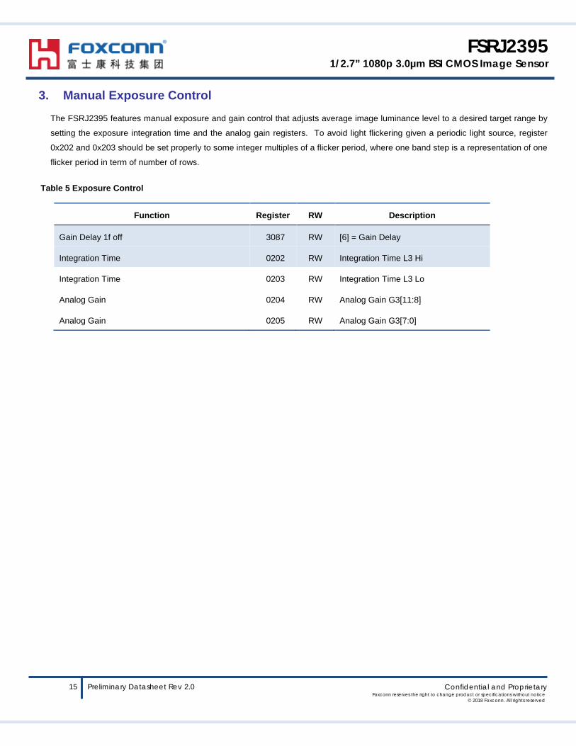
3. Manual Exposure Control The FSRJ2395 features manual exposure and gain control that adjusts average image luminance level to a desired target range by
setting the exposure integration time and the analog gain registers. To avoid light flickering given a periodic light source, register
0x202 and 0x203 should be set properly to some integer multiples of a flicker period, where one band step is a representation of one
flicker period in term of number of rows.
Table 5 Exposure Control
Function Register RW Description
Gain Delay 1f off 3087 RW [6] = Gain Delay
Integration Time 0202 RW Integration Time L3 Hi
Integration Time 0203 RW Integration Time L3 Lo
Analog Gain 0204 RW Analog Gain G3[11:8]
Analog Gain 0205 RW Analog Gain G3[7:0]

FSRJ2395 1/2.7” 1080p 3.0µm BSI CMOS Image Sensor
16 Preliminary Datasheet Rev 2.0 Confidential and Proprietary Foxconn reserves the right to change product or specifications without notice
© 2018 Foxconn. All rights reserved
4. ISP Test Pattern
The FSRJ2395 offers one type of ISP test pattern, color bar.
Figure 10 Color Bar
Table 6 Color Bar Test Pattern
Function Register RW Description
Color Bar Enable 3C00 RW [2] 0: Color Bar off, 1 : Color Bar on
5. MIPI Interface FSRJ2395 supports MIPI CSI-2 compliance interface. Data of 10-bit raw is output through up to two pair of differential data lanes
(SDPx, SDNx) and one pair of differential clock lane (SCP, SCN).

FSRJ2395 1/2.7” 1080p 3.0µm BSI CMOS Image Sensor
17 Preliminary Datasheet Rev 2.0 Confidential and Proprietary Foxconn reserves the right to change product or specifications without notice
© 2018 Foxconn. All rights reserved
6. Electrical Characteristics (TBD) Table 7 Absolute Maximum Ratings (voltages referenced to ground)
Symbol Absolute Maximum Rating Unit
Analog Supply Voltage VDD-A 4.5 V
I/O Digital Supply Voltage VDD-IO 4.5 V
Input Voltages VI -0.3 ~ +3.0 V
Ambient Operating Temperature TA -30 ~ 70 °C
Storage Temperature TS -40 ~ 95 °C
Table 8 DC Characteristics (-20°C <TA<70 C), voltages referenced to ground
Supply Voltages Symbol Min Typical Max Unit
Analog Supply Voltage (AVDD) VDD-A 3.20 3.30 3.60 V
I/O Digital Supply Voltage (IOVDD) VDD-IO 1.70 1.80 AVDD V
Digital Inputs Symbol Min Typical Max Unit
Input Voltage Low VIL 0 - 0.2 x VDD-IO V
Input Voltage High VIH 0.8 x VDD-IO - VDD-IO V
Input Capacitor CIN - - 10 pF
Digital Outputs (20 pF load capacitance) Symbol Min Typical Max Unit
Output Voltage High VOH VDD-IO – 0.2 - - V
Output Voltage Low VOL - - 0.2 V
Power Consumption Symbol Min Typical Max Unit
Supply Current (VDD-A = 3.3V, 30fps 1080p) IDD-A - TBD - mA
Supply Current (VDD-IO = 1.8V, 30fps 1080p) IDD-IO - TBD - mA
Stand by Current (without external clock) ISTBY - TBD - mA
Standby current with active external clock ISLEEP - TBD - mA

FSRJ2395 1/2.7” 1080p 3.0µm BSI CMOS Image Sensor
18 Preliminary Datasheet Rev 2.0 Confidential and Proprietary Foxconn reserves the right to change product or specifications without notice
© 2018 Foxconn. All rights reserved
7. Register Descriptions
Write Slave Address: 0x6c, Read Slave Address: 0x6d
Address Register Name Default Value Description
0000 MODEL ID
8'h02 sensor id Hi
0001 8'h07 sensor id Lo
0002 REVISION 8'h01 silicon revision number
0100 MODE 8'h00 mode select: 0 – software standby, 1 – streaming
0101 ORIENTATION 8'h00 [1] vflip [0] hmirror
0103 SOFTWARE 8'h00 [0] software reset
0202 EXPO
8'h00 integration time L3 Hi
0203 8'hF4 integration time L3 Lo
0204 anagain04 8'h00 [7:4] anagain G2 [11:8] [3:0] anagain G3[11:8]
0205 anagain05 8'h00 anagain G3[7:0]
0206 anagain06 8'h00 anagain G2[7:0]
0210 AWB R Gain
8'h04 [7:4] not used [3:0] awb r gain[11:8]
0211 8'h00 [7:0] awb r gain[7:0]
0212 AWB B Gain
8'h04 [7:4] not used [3:0] awb b gain[11:8]
0213 8'h00 [7:0] awb b gain[7:0]
0214 AWB G Gain
8'h04 [7:4] not used [3:0] awb g gain[11:8]
0215 8'h00 [7:0] awb g gain[7:0]
0216 DIGITAL GAIN
8'h01 [7:4] not used [3:0] digital gain[11:8]
0217 8'h00 [7:0] digital gain[7:0]
0303 sys div 8'h02 [7:6] Reserved [5:0] sys div
0304 CLK REG0304 8'h00
[7:5] Reserved [4] loopx2 [3:2] post div [1:0] mipi div
0305 pre div 8'h02 [1:0] pre div
0307 multiplier 8'h64 multiplier
0340 frame rows
8'h04 frame length Hi
0341 8'h50 frame length Lo

FSRJ2395 1/2.7” 1080p 3.0µm BSI CMOS Image Sensor
19 Preliminary Datasheet Rev 2.0 Confidential and Proprietary Foxconn reserves the right to change product or specifications without notice
© 2018 Foxconn. All rights reserved
Address Register Name Default Value Description
0342 row pixels
8'h09 Line length Hi
0343 8'h6C Line length Lo
0344 x_addr_start
8'h00 X-address Hi of top left corner of array
0345 8'h00 X-address Lo of top left corner of array
0346 y_addr_start
8'h00 Y-address Hi of top left corner of array
0347 8'h00 Y-address Lo of top left corner of array
0348 x_addr_end
8'h07 X-address Hi of bottom right corner of array
0349 8'h8F X-address Lo of bottom right corner of array
034A y_addr_end
8'h04 Y-address Hi of bottom right corner of array
034B 8'h3F Y-address Lo of bottom right corner of array
034C x_output_size
8'h07 sensor data output width Hi
034D 8'h80 sensor data output width Lo
034E y_output_size
8'h04 sensor data output height Hi
034F 8'h38 sensor data output height Lo
0381 x_even_inc 8'h01 horizontal even pixel increment
0383 x_odd_inc 8'h01 horizontal odd pixel increment
0385 y_even_inc 8'h01 vertical even pixel increment
0387 y_odd_inc 8'h01 vertical odd pixel increment
3000 tmreg0 8'h82
[7] frame1off en [6] fsynout re [5] asread addr bin [4] sread clk re [3:2] test out2gpio [1] sof sel 0] autoframe en
3001 tmreg1 8'h80
[7] fsyn select tmreg6, tmreg7 [5] fsyn en at gpio [4] fsyn gpio input re [3:0] vc adjust
3002 tmreg2 8'h00 fsyn output delay Hi
3003 tmreg3 8'h00 fsyn output delay Lo
3004 tmreg4 8'h00 fsyn reset horizontal Hi
3005 tmreg5 8'h00 fsyn reset horizontal Lo
3006 tmreg6 8'h00 fsyn reset vertical Hi
3007 tmreg7 8'h00 fsyn reset vertical Lo
3008 tmreg8 8'h00 horizontal window offset Hi
3009 tmreg9 8'h04 horizontal window offset Lo

FSRJ2395 1/2.7” 1080p 3.0µm BSI CMOS Image Sensor
20 Preliminary Datasheet Rev 2.0 Confidential and Proprietary Foxconn reserves the right to change product or specifications without notice
© 2018 Foxconn. All rights reserved
Address Register Name Default Value Description
300A tmrega 8'h00 vertical window offset Hi
300B tmregb 8'h04 vertical window offset Lo
3010 tmreg10 8'h01 tx start timing for asread
3011 tmreg11 8'h5E
3012 tmreg12 8'h01 tx end timing for asread
3013 tmreg13 8'hFE
3014 tmreg14 8'h01 tx start timing to recovered
3015 tmreg15 8'h5E
3016 tmreg16 8'h01 tx end timing to recovered
3017 tmreg17 8'hFE
3018 tmreg18 8'h00 [1] bank st hold [0] tx hold enable
3020 tmreg20 8'h00
[7] fsyn en2 [6] fsyn lv en [5] fsyn out sel [4] not used [3] bsi sread [2] reserved [1] sof 2 sel [0] sof sel2
3021 tmreg21 8'h11 [6:4] hbin factor [3] vbin enable [2:0] vbin factor
3022 tmreg22 8'h05
[7] frame2 off [6] frame2 frp [5] frame2 grp en [4] sread bank enb2 [3] sread bank enb1 [2] sread ext en
3087 aec7 8'h30 [6] gain delay 1f off
3088 aec8 8'h04 [2:0] againmax sel
3108 control1 8'h4F
[7] dcblc_en [6] blc always on [5] bc timer off 0: force trigger on 1: force trigger off [4] bit_width 0: 10bit 1: 12bit [3:0] auto blc enable
3109 target 8'h40 blc target

FSRJ2395 1/2.7” 1080p 3.0µm BSI CMOS Image Sensor
21 Preliminary Datasheet Rev 2.0 Confidential and Proprietary Foxconn reserves the right to change product or specifications without notice
© 2018 Foxconn. All rights reserved
Address Register Name Default Value Description
3112 dc_ratio 8'h00 dc_ratio: = img/black * 256
3401 group1 8'h00 group1 start
3402 group2 8'h00 group2 start
3403 group3 8'h00 group3 start
3404 group4 8'h00 group0 len
3405 group5 8'h00 group1 len
3406 group6 8'h00 group2 len
3407 group7 8'h00 group3 len
340F groupf WO
[7] delay read [6] fast read [5] delay write2 [4] delay write [3] fast write [2:0] group sel
3410 group10 8'h00 group4 start
3411 group11 8'h00 group5 start
3412 group12 8'h00 group6 start
3413 group13 8'h00 group7 start
3414 group14 8'h00 group4 len
3415 group15 8'h00 group5 len
3416 group16 8'h00 group6 len
3417 group17 8'h00 group7 len
3585 i2c5 8'h00 [4] bypass pll1
3800 mipi0 8'h00 lp wakeup Hi
3801 mipi1 8'h54 lp wakeup Lo
3802 mipi2 8'h00 lp data Hi
3803 mipi3 8'h00 lp data Lo
3804 mipi4 8'h00 escape cmd
3805 mipi5 8'h05 hs trail
3806 mipi6 8'h06 hs prepare
3807 mipi7 8'h06 clk prepare
3808 mipi8 8'h19 clk zero
3809 mipi9 8'h63 [7:4] hs zero [3:0] tlpx
380A mipia 8'h6D [7:4] clk trail [3:0] clk post

FSRJ2395 1/2.7” 1080p 3.0µm BSI CMOS Image Sensor
22 Preliminary Datasheet Rev 2.0 Confidential and Proprietary Foxconn reserves the right to change product or specifications without notice
© 2018 Foxconn. All rights reserved
Address Register Name Default Value Description
380B mipib 8'hE6 [7:6] clk pre [5] bclko re [4:0] hs exit
380C mipic 8'h21
[7] stop sel [6] Reserved [5] clk free running [4] prbs en [3:0] fe delay
380D mipid 8'h00
[7] escape start [6] clk ulps start [5] data ulps end [4] clk ulps end [3] lp dly [2] sleep [1:0] valid trigger
380E mipie 8'h30 [7] gt mansel [6:4] gt clkadj [1:0] valid select
380F mipif 8'h00 [7:3] Not Used [2] shortpkt num [1:0] virtual channel
3900 fmt0 8'h00 smia solid color r
3901 fmt1 8'h00 smia solid color gr
3902 fmt2 8'h00 smia solid color b
3903 fmt3 8'h00 smia solid color gb
3904 fmt4 8'h01
[7:6] Not Used [5] emb fmt [4] fc down [3:0] fc count 0/f: no drop, x: drop x
3905 fmt5 8'h01
[7] clip en [6] emb en [5:4] emb num [3:0] format 4'hb: raw10
3906 fmt6 8'h12 [5:0] emb dt
3907 fmt7 8'h00
[7] slave first line emb [6:2] Reserved [1:0] vvalid delay sel 2'b00: no delay 2'b01: delay 1 row 2'b10: delay 2 rows 2'b11: delay 3 rows
3A80 OTP ctrl0 8'h00
[7] OTP enable [6:4] Not used. [3] auto load enable [2:0] Not used

FSRJ2395 1/2.7” 1080p 3.0µm BSI CMOS Image Sensor
23 Preliminary Datasheet Rev 2.0 Confidential and Proprietary Foxconn reserves the right to change product or specifications without notice
© 2018 Foxconn. All rights reserved
Address Register Name Default Value Description
3A81 OTP ctrl1 8'h00
[7:5] Not used [4] auto load enable [3] I2C sequential write mode enable [2] Not used [1] OTP read mode enable [0] OTP program mode enable
3A82 OTP ADDRESS 8'h50 [7:4] end address[11:8] [3:0] start address[11:8]
3A83 START ADDRESS 8'h00 start address[7:0]
3A84 END ADDRESS 8'hFF end address[7:0]
3A85 OTP_TH 8'h03 timing threshold >25ns
3A86 OTP TH_I2C 8'h03 timing threshold1 >20ns
3A87 OTP TH1 8'h2a timing threshold1 >500ns
3A88 OTP TH2 8'h10 timing threshold2 normal: >200ns blankcheck:>1500ns
3A89 OTP TH3 8'h55 timing threshold3 >1000ns
3A93 AUTO LOAD START ADDRESS 8'h00 [7:4] not used
[3:0] high 4bits of start address of auto load
3A94 OTP AUTO LOAD PW 8'h14 Auto load timing threshold Only active in auto load (read) mode: TH_I2C > (THread + PW +2)
3A20 OTP DRIVER CTRL 1 8'h1D [6:4] CP_TRIM_H [3:0] IPGM_TRIM_H
3A21 OTP DRIVER CTRL2 8'h02 VRDAPVFY_TRIM_H
3C00 RAWTEST_00 8'h00
[7:4] Not used. [3] color bar move enable [2] color bar enable [1] flip auto enable [0] mirror auto enable
3C01 ISP_01 8'h10
[7:4] Not used [3] hskip2 [2] rawgain dither enable [1] raw gain black offset enable [0] raw gain enable
3C02 ISP_02 8'h31 [7] pvalid_bin [6:0] Not used

FSRJ2395 1/2.7” 1080p 3.0µm BSI CMOS Image Sensor
24 Preliminary Datasheet Rev 2.0 Confidential and Proprietary Foxconn reserves the right to change product or specifications without notice
© 2018 Foxconn. All rights reserved
Address Register Name Default Value Description
3C03 ISP_03 8'h00
[7:6] Not used [5:4] diggain update delay control 2’b00: update at the end of current frame 2’b01: update at the end of next frame 2’b1x: update at once [3:0] Not used
3C04 ISP_04 8'hF8
[7] black bpc enable [6] white bpc enable [5:3] notused [2:0] ISP output selection 3'b000: sensor raw 3'b001: bpc_dns raw
3C05 ISP_05 8'h01 [7:1] Not used [0] Force bit enable
3C06 ISP_06 8'h00 [7:0] Not used
3C07 ISP_07 8'h00 [7] pixel order control [6:0]Not used
3C14 ISP_14 8'h00
[7:6] Not used [5:4] bpc manual pixel order [3:2] rawg manual pixel order [1:0] Not used
3DA3 RO [4:0] vinc odd increase step
3DA4 RO [3:0] horizontal start address [11:8]
3DA5 RO [7:0] horizontal start address[7:0]
3DA6 RO [3:0] vertical start address[11:8]
3DA7 RO [7:0] vertical start adress[7:0]
3F00 AVG_00 00 Horizontal roi offset hi
3F01 AVG_01 00 horizontal roi offset lo
3F02 AVG_02 00 vertical roi offset hi
3D00 BPC0 8'hFB
[7] two neighbor defective pixel (dp) enable [6] two dimensional dp enable [5:4] edge option for image boundary [3] manual cluster detection threshold enable 1'b0: use manual cluster threshold 1'b1: use auto threshold adjust with sensor gain If sensor gain is more larger, threshold is more larger [2] manual dp enable 1'b1: manual smooth_en, color_en, thresh2, thresh3, thresh4, wthre, bthre 1'b0: adjust smooth_en, color_en, thresh2, thresh3, thresh4, wthre, bthre with sensor gain [1:0] vertical dp number
3F00 AVG_00 8'h00 Horizontal roi offset hi

FSRJ2395 1/2.7” 1080p 3.0µm BSI CMOS Image Sensor
25 Preliminary Datasheet Rev 2.0 Confidential and Proprietary Foxconn reserves the right to change product or specifications without notice
© 2018 Foxconn. All rights reserved
Address Register Name Default Value Description
3F01 AVG_01 8'h00 horizontal roi offset lo
3F02 AVG_02 8'h00 vertical roi offset hi
3F03 AVG_03 8'h00 vertical roi offset lo
3F04 AVG_04 8'h07 horizontal roi size hi
3F05 AVG_05 8'h80 horizontal roi size lo
3F06 AVG_06 8'h04 verticall roi size hi
3F07 AVG_07 8'h38 vertical roi size lo
3F08 AVG_08 8'h11
[7:6] Not Used [5] avg last 1 cycle more [4] roi enable [3:2] avg data sel 2'b00: raw 2'b01: g 2'b1x: y [1:0] avg input selection 2'b00: sensor 2'b01: bpc

FSRJ2395 1/2.7” 1080p 3.0µm BSI CMOS Image Sensor
26 Preliminary Datasheet Rev 2.0 Confidential and Proprietary Foxconn reserves the right to change product or specifications without notice
© 2018 Foxconn. All rights reserved
8. Optical Specifications
8.1 Lens Chief Ray Angle
Figure 11 Chief Ray Angle
Field Image Height(mm) CRA(°)0.00 0.00 00.10 0.33 0.90.20 0.66 1.80.30 0.99 2.70.40 1.32 3.60.50 1.65 4.50.60 1.98 5.40.70 2.31 6.30.80 2.64 7.20.90 2.97 8.11.00 3.30 9

FSRJ2395 1/2.7” 1080p 3.0µm BSI CMOS Image Sensor
27 Preliminary Datasheet Rev 2.0 Confidential and Proprietary Foxconn reserves the right to change product or specifications without notice
© 2018 Foxconn. All rights reserved
9. Mechanical Specifications
9.1 Physical Specifications
Figure 12 CSP Top, Bottom and Side View

FSRJ2395 1/2.7” 1080p 3.0µm BSI CMOS Image Sensor
28 Preliminary Datasheet Rev 2.0 Confidential and Proprietary Foxconn reserves the right to change product or specifications without notice
© 2018 Foxconn. All rights reserved
Table 9 CSP Package Dimensions

FSRJ2395 1/2.7” 1080p 3.0µm BSI CMOS Image Sensor
29 Preliminary Datasheet Rev 2.0 Confidential and Proprietary Foxconn reserves the right to change product or specifications without notice
© 2018 Foxconn. All rights reserved
Revision History
Rev. 1.0 10/12/2018: Preliminary draft.
Rev. 2.0 12/19/2018: Update Default Setting.