120-V Boot, 4-A Peak, High Frequency High-Side and Low ... · PDF filepwm controller +12v...
39
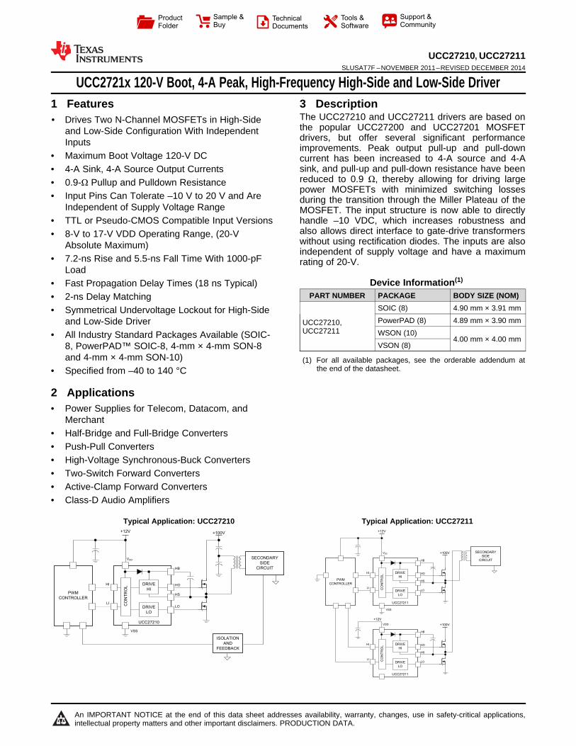
PWM CONTROLLER +12V +100V SECONDARY SIDE CIRCUIT HI CONTROL DRIVE LO DRIVE HI VDD UCC27211 VSS LI HB HO HS LO +12V HI CONTROL DRIVE LO DRIVE HI VDD UCC27211 LI HB HO HS LO +100V PWM CONTROLLER +12V ISOLATION AND FEEDBACK +100V SECONDARY SIDE CIRCUIT HI CONTROL DRIVE LO DRIVE HI VDD UCC27210 VSS LI HB HO HS LO Product Folder Sample & Buy Technical Documents Tools & Software Support & Community An IMPORTANT NOTICE at the end of this data sheet addresses availability, warranty, changes, use in safety-critical applications, intellectual property matters and other important disclaimers. PRODUCTION DATA. UCC27210, UCC27211 SLUSAT7F – NOVEMBER 2011 – REVISED DECEMBER 2014 UCC2721x 120-V Boot, 4-A Peak, High-Frequency High-Side and Low-Side Driver 1 1 Features 1• Drives Two N-Channel MOSFETs in High-Side and Low-Side Configuration With Independent Inputs • Maximum Boot Voltage 120-V DC • 4-A Sink, 4-A Source Output Currents • 0.9-Ω Pullup and Pulldown Resistance • Input Pins Can Tolerate –10 V to 20 V and Are Independent of Supply Voltage Range • TTL or Pseudo-CMOS Compatible Input Versions • 8-V to 17-V VDD Operating Range, (20-V Absolute Maximum) • 7.2-ns Rise and 5.5-ns Fall Time With 1000-pF Load • Fast Propagation Delay Times (18 ns Typical) • 2-ns Delay Matching • Symmetrical Undervoltage Lockout for High-Side and Low-Side Driver • All Industry Standard Packages Available (SOIC- 8, PowerPAD™ SOIC-8, 4-mm × 4-mm SON-8 and 4-mm × 4-mm SON-10) • Specified from –40 to 140 °C 2 Applications • Power Supplies for Telecom, Datacom, and Merchant • Half-Bridge and Full-Bridge Converters • Push-Pull Converters • High-Voltage Synchronous-Buck Converters • Two-Switch Forward Converters • Active-Clamp Forward Converters • Class-D Audio Amplifiers space 3 Description The UCC27210 and UCC27211 drivers are based on the popular UCC27200 and UCC27201 MOSFET drivers, but offer several significant performance improvements. Peak output pull-up and pull-down current has been increased to 4-A source and 4-A sink, and pull-up and pull-down resistance have been reduced to 0.9 Ω, thereby allowing for driving large power MOSFETs with minimized switching losses during the transition through the Miller Plateau of the MOSFET. The input structure is now able to directly handle –10 VDC, which increases robustness and also allows direct interface to gate-drive transformers without using rectification diodes. The inputs are also independent of supply voltage and have a maximum rating of 20-V. Device Information (1) PART NUMBER PACKAGE BODY SIZE (NOM) UCC27210, UCC27211 SOIC (8) 4.90 mm × 3.91 mm PowerPAD (8) 4.89 mm × 3.90 mm WSON (10) 4.00 mm × 4.00 mm VSON (8) (1) For all available packages, see the orderable addendum at the end of the datasheet. Typical Application: UCC27210 Typical Application: UCC27211
Transcript of 120-V Boot, 4-A Peak, High Frequency High-Side and Low ... · PDF filepwm controller +12v...
PWM
CONTROLLER
+12V
+100V SECONDARY
SIDE
CIRCUIT
HI
CO
NT
RO
L
DRIVE
LO
DRIVE
HI
VDD
UCC27211
VSS
LI
HB
HO
HS
LO
+12V
HI
CO
NT
RO
L
DRIVE
LO
DRIVE
HI
VDD
UCC27211
LI
HB
HO
HS
LO
+100V
PWM
CONTROLLER
+12V
ISOLATION
AND
FEEDBACK
+100V
SECONDARY
SIDE
CIRCUIT
HI
CO
NT
RO
L
DRIVE
LO
DRIVE
HI
VDD
UCC27210
VSS
LI
HB
HO
HS
LO
Product
Folder
Sample &Buy
Technical
Documents
Tools &
Software
Support &Community
An IMPORTANT NOTICE at the end of this data sheet addresses availability, warranty, changes, use in safety-critical applications,intellectual property matters and other important disclaimers. PRODUCTION DATA.
UCC27210, UCC27211SLUSAT7F –NOVEMBER 2011–REVISED DECEMBER 2014
UCC2721x 120-V Boot, 4-A Peak, High-Frequency High-Side and Low-Side Driver
1
1 Features1• Drives Two N-Channel MOSFETs in High-Side
and Low-Side Configuration With IndependentInputs
• Maximum Boot Voltage 120-V DC• 4-A Sink, 4-A Source Output Currents• 0.9-Ω Pullup and Pulldown Resistance• Input Pins Can Tolerate –10 V to 20 V and Are
Independent of Supply Voltage Range• TTL or Pseudo-CMOS Compatible Input Versions• 8-V to 17-V VDD Operating Range, (20-V
Absolute Maximum)• 7.2-ns Rise and 5.5-ns Fall Time With 1000-pF
Load• Fast Propagation Delay Times (18 ns Typical)• 2-ns Delay Matching• Symmetrical Undervoltage Lockout for High-Side
and Low-Side Driver• All Industry Standard Packages Available (SOIC-
8, PowerPAD™ SOIC-8, 4-mm × 4-mm SON-8and 4-mm × 4-mm SON-10)
• Specified from –40 to 140 °C
2 Applications• Power Supplies for Telecom, Datacom, and
Merchant• Half-Bridge and Full-Bridge Converters• Push-Pull Converters• High-Voltage Synchronous-Buck Converters• Two-Switch Forward Converters• Active-Clamp Forward Converters• Class-D Audio Amplifiers
space
3 DescriptionThe UCC27210 and UCC27211 drivers are based onthe popular UCC27200 and UCC27201 MOSFETdrivers, but offer several significant performanceimprovements. Peak output pull-up and pull-downcurrent has been increased to 4-A source and 4-Asink, and pull-up and pull-down resistance have beenreduced to 0.9 Ω, thereby allowing for driving largepower MOSFETs with minimized switching lossesduring the transition through the Miller Plateau of theMOSFET. The input structure is now able to directlyhandle –10 VDC, which increases robustness andalso allows direct interface to gate-drive transformerswithout using rectification diodes. The inputs are alsoindependent of supply voltage and have a maximumrating of 20-V.
Device Information(1)
PART NUMBER PACKAGE BODY SIZE (NOM)
UCC27210,UCC27211
SOIC (8) 4.90 mm × 3.91 mmPowerPAD (8) 4.89 mm × 3.90 mmWSON (10)
4.00 mm × 4.00 mmVSON (8)
(1) For all available packages, see the orderable addendum atthe end of the datasheet.
Typical Application: UCC27210 Typical Application: UCC27211

2
UCC27210, UCC27211SLUSAT7F –NOVEMBER 2011–REVISED DECEMBER 2014 www.ti.com
Product Folder Links: UCC27210 UCC27211
Submit Documentation Feedback Copyright © 2011–2014, Texas Instruments Incorporated
Table of Contents1 Features .................................................................. 12 Applications ........................................................... 13 Description ............................................................. 14 Revision History..................................................... 25 Description (Continued) ........................................ 46 Pin Configuration and Functions ......................... 47 Specifications......................................................... 5
7.1 Absolute Maximum Ratings ...................................... 57.2 ESD Ratings ............................................................ 67.3 Recommended Operating Conditions....................... 67.4 Thermal Information .................................................. 67.5 Electrical Characteristics........................................... 77.6 Switching Characteristics: Propagation Delays ........ 87.7 Switching Characteristics: Delay Matching ............... 87.8 Switching Characteristics: Output Rise and Fall
Time ........................................................................... 87.9 Switching Characteristics: Miscellaneous ................. 87.10 Typical Characteristics .......................................... 10
8 Detailed Description ............................................ 13
8.1 Overview ................................................................. 138.2 Functional Block Diagram ....................................... 148.3 Feature Description................................................. 148.4 Device Functional Modes........................................ 15
9 Application and Implementation ........................ 169.1 Application Information............................................ 169.2 Typical Application ................................................. 16
10 Power Supply Recommendations ..................... 2111 Layout................................................................... 21
11.1 Layout Guidelines ................................................. 2111.2 Layout Example .................................................... 2211.3 Thermal Considerations ........................................ 22
12 Device and Documentation Support ................. 2312.1 Documentation Support ........................................ 2312.2 Related Links ........................................................ 2312.3 Trademarks ........................................................... 2312.4 Electrostatic Discharge Caution............................ 2312.5 Glossary ................................................................ 23
13 Mechanical, Packaging, and OrderableInformation ........................................................... 23
4 Revision HistoryNOTE: Page numbers for previous revisions may differ from page numbers in the current version.
Changes from Revision E (August 2013) to Revision F Page
• Added Pin Configuration and Functions section, ESD Ratings table, Feature Description section, Device FunctionalModes, Application and Implementation section, Power Supply Recommendations section, Layout section, Deviceand Documentation Support section, and Mechanical, Packaging, and Orderable Information section .............................. 1
Changes from Revision D (November, 2012) to Revision E Page
• Added Note 2 to the Terminal Functions Table...................................................................................................................... 5• Changed Repetitive pulse data from -18 V to -(24V-VDD). ................................................................................................... 5• Added additional details to Note 2.......................................................................................................................................... 5• Changed Voltage on HS, VHS (repetitive pulse <100 ns) data from -15 to -(24V-VDD)......................................................... 6• Deleted 2.4-mA operating current min range in both places.................................................................................................. 7• Changed operating current max range extended to 5.2 in both places. ................................................................................ 7• Deleted 1.5 min Boot voltage operating current range........................................................................................................... 7• Changed Boot voltage operating current max range from 4.2 to 5.0. .................................................................................... 7• Changed HB to VSS operating current max range from 1.1 to 1.2. ........................................................................................ 7• Changed LO Gate Driver's Low-level output voltage max range from 0.17 to 0.19............................................................... 7• Changed HO GATE Driver's Low-level output voltage max range from 0.17 to 0.19. ........................................................... 7
Changes from Revision C (March, 2012) to Revision D Page
• Changed capacitor range from 1.0 µF to 4.7 µF. ................................................................................................................... 5• Added Terminal Functions Note to HI and LI pin description................................................................................................. 5• Changed bullet 2 in the Layout Recommendations. ........................................................................................................... 21• Added Note: For systems using... ........................................................................................................................................ 21

3
UCC27210, UCC27211www.ti.com SLUSAT7F –NOVEMBER 2011–REVISED DECEMBER 2014
Product Folder Links: UCC27210 UCC27211
Submit Documentation FeedbackCopyright © 2011–2014, Texas Instruments Incorporated
• Added Note: Care should be taken... ................................................................................................................................... 21
Changes from Revision B (February) to Revision C Page
• Changed VDD operating current max range of 4.3 to 4.4 in both places. ............................................................................... 7• Changed Boot voltage operating current max range from 4.0 to 4.2. .................................................................................... 7• Changed HB to VSS quiescent current max range from 0.13 to 1.0. ...................................................................................... 7• Changed HB to VSS operating current max range from 0.9 to 1.1. ........................................................................................ 7• Added Input UCC27210/11 (DDA Only) values. .................................................................................................................... 7• Added Under-Voltage Lockout (UVLO) DDA only values, two places. .................................................................................. 7• Changed LO Gate Driver's Low-level output voltage max range from 0.15 to 0.17............................................................... 7• Changed LO Gate Driver's VLOH max range from 0.27 to 0.29. ............................................................................................. 7• Changed HO GATE Driver's Low-level output voltage max range from 0.15 to 0.17. ........................................................... 7• Changed VLI falling to VLO falling min value from 17 to 15. .................................................................................................... 8• Changed VHI falling to VHO falling min value from 17 to 15. ................................................................................................... 8• Changed VLI rising to VLO rising min value from 18 to 15....................................................................................................... 8• Changed VHI rising to VHO rising min value from 18 to 15...................................................................................................... 8• Changed Figure 17, Output Current vs. Output Voltage. ..................................................................................................... 12

VDD
HB
HO
HS
NC
LO
VSS
LI
HI
NC
10
9
1
2
3
4
5
8
7
6
SON-10 (DPR)TOP VIEW
1
2
3
4
8
7
6
5
VDD
HB
HO
HS
VSS
Power PadTM
SOIC-8 (DDA)
TOP VIEW
Exposed
Thermal
Die Pad
LO
LI
HI
1
2
3
4
8
7
6
5
VDD
HB
HO
HS
LO
VSS
LI
HI
SOIC-8 (D)
TOP VIEW
1
2
3
4
8
7
6
5
VDD
HB
HO
HS
VSS
SON-8 (DRM)
TOP VIEW
Exposed
Thermal
Die Pad*
LO
LI
HI
4
UCC27210, UCC27211SLUSAT7F –NOVEMBER 2011–REVISED DECEMBER 2014 www.ti.com
Product Folder Links: UCC27210 UCC27211
Submit Documentation Feedback Copyright © 2011–2014, Texas Instruments Incorporated
5 Description (Continued)The switching node (HS pin) of the UCC2721x can handle –18 V maximum which allows the high-side channel tobe protected from inherent negative voltages caused parasitic inductance and stray capacitance. The UCC27210(Pseudo-CMOS inputs) and UCC27211 (TTL inputs) have increased hysteresis allowing for interface to analog ordigital PWM controllers with enhanced noise immunity.
The low-side and high-side gate drivers are independently controlled and matched to 2 ns between the turnonand turnoff of each other.
An on-chip 120-V rated bootstrap diode eliminates the external discrete diodes. Undervoltage lockout is providedfor both the high-side and the low-side drivers providing symmetric turnon and turnoff behavior and forcing theoutputs low if the drive voltage is below the specified threshold.
Both devices are offered in 8-pin SOIC (D), PowerPAD SOIC-8 (DDA), 4-mm × 4-mm SON-8 (DRM) and SON-10 (DPR) packages.
6 Pin Configuration and Functions

5
UCC27210, UCC27211www.ti.com SLUSAT7F –NOVEMBER 2011–REVISED DECEMBER 2014
Product Folder Links: UCC27210 UCC27211
Submit Documentation FeedbackCopyright © 2011–2014, Texas Instruments Incorporated
(1) For cold temperature applications we recommend the upper capacitance range. Attention should also be made to PCB layout - seeLayout.
(2) HI or LI input is assumed to connect to a low impedance source signal. The source output impedance is assumed less than 100 Ω. If thesource impedance is greater than 100 Ω, add a bypassing capacitor, each, between HI and VSS and between LI and VSS. The addedcapacitor value depends on the noise levels presented on the pins, typically from 1 nF to 10 nF should be effective to eliminate thepossible noise effect. When noise is present on two pins, HI or LI, the effect is to cause HO and LO malfunctions to have wrong logicoutputs.
(3) The PowerPAD™ is not directly connected to any leads of the package. However it is electrically and thermally connected to thesubstrate which is the ground of the device.
Pin FunctionsPIN
I/O DESCRIPTIONNAME D/DDA/DRM DPR
VDD 1 1 P Positive supply to the lower-gate driver. Decouple this pin to VSS (GND). Typicaldecoupling capacitor range is 0.22 µF to 4.7 µF (See (1)).
HB 2 2 P
High-side bootstrap supply. The bootstrap diode is on-chip but the external bootstrapcapacitor is required. Connect positive side of the bootstrap capacitor to this pin.Typical range of HB bypass capacitor is 0.022 µF to 0.1 µF. The capacitor value isdependant on the gate charge of the high-side MOSFET and should also be selectedbased on speed and ripple criteria
HO 3 3 O High-side output. Connect to the gate of the high-side power MOSFET.
HS 4 4 P High-side source connection. Connect to source of high-side power MOSFET.Connect the negative side of bootstrap capacitor to this pin.
HI 5 7 I High-side input. (2)
LI 6 8 I Low-side input. (2)
VSS 7 9 G Negative supply terminal for the device which is generally grounded.LO 8 10 O Low-side output. Connect to the gate of the low-side power MOSFET.N/C — 5/6 — Not connected.
PowerPAD™ (3) Pad Pad G
Used on the DDA, DRM and DPR packages only. Electrically referenced to VSS(GND). Connect to a large thermal mass trace or GND plane to dramatically improvethermal performance.
(1) Stresses beyond those listed under Absolute Maximum Ratings may cause permanent damage to the device. These are stress ratingsonly, and functional operation of the device at these or any other conditions beyond those indicated under Recommended OperatingConditions is not implied. Exposure to absolute-maximum-rated conditions for extended periods may affect device reliability.
(2) All voltages are with respect to VSS unless otherwise noted. Currents are positive into, negative out of the specified terminal.(3) Verified at bench characterization. VDD is the value used in an application design.
7 Specifications
7.1 Absolute Maximum Ratings (1)
over operating free-air temperature range (unless otherwise noted)MIN MAX UNIT
Supply voltage range, VDD(2), VHB - VHS –0.3 20
V
Input voltages on LI and HI, VLI, VHI –10 20
Output voltage on LO, VLODC –0.3 VDD + 0.3Repetitive pulse <100 ns (3) –2 VDD + 0.3
Output voltage on HO, VHODC VHS – 0.3 VHB + 0.3Repetitive pulse <100 ns (3) VHS – 2 VHB + 0.3
Voltage on HS, VHSDC –1 115Repetitive pulse <100 ns (3) –(24 V-VDD) 115
Voltage on HB, VHB –0.3 120Operating virtual junction temperature, TJ –40 150
°CLead temperature (soldering, 10 sec.) 300Storage temperature, Tstg –65 150 °C

6
UCC27210, UCC27211SLUSAT7F –NOVEMBER 2011–REVISED DECEMBER 2014 www.ti.com
Product Folder Links: UCC27210 UCC27211
Submit Documentation Feedback Copyright © 2011–2014, Texas Instruments Incorporated
(1) JEDEC document JEP155 states that 500-V HBM allows safe manufacturing with a standard ESD control process.(2) JEDEC document JEP157 states that 250-V CDM allows safe manufacturing with a standard ESD control process.
7.2 ESD RatingsVALUE UNIT
V(ESD) Electrostatic dischargeHuman body model (HBM), per ANSI/ESDA/JEDEC JS-001 (1) ±2000
VCharged-device model (CDM), per JEDEC specification JESD22-C101 (2)
±1000
7.3 Recommended Operating Conditionsall voltages are with respect to VSS; currents are positive into and negative out of the specified terminal. –40°C < TJ = TA <140°C (unless otherwise noted)
MIN TYP MAX UNITSupply voltage range, VDD, VHB-VHS 8 12 17
VVoltage on HS, VHS –1 105Voltage on HS, VHS (repetitive pulse <100 ns) –(24V-VDD) 110
Voltage on HB, VHBVHS +8,VDD –1
VHS +17,115
Voltage slew rate on HS 50 V/nsOperating junction temperature range –40 140 °C
(1) The junction-to-ambient thermal resistance under natural convection is obtained in a simulation on a JEDEC-standard, high-K board, asspecified in JESD51-7, in an environment described in JESD51-2a.
(2) The junction-to-case (top) thermal resistance is obtained by simulating a cold plate test on the package top. No specific JEDEC-standard test exists, but a close description can be found in the ANSI SEMI standard G30-88.
(3) The junction-to-board thermal resistance is obtained by simulating in an environment with a ring cold plate fixture to control the PCBtemperature, as described in JESD51-8.
(4) The junction-to-top characterization parameter, ψJT, estimates the junction temperature of a device in a real system and is extractedfrom the simulation data for obtaining RθJA, using a procedure described in JESD51-2a (sections 6 and 7).
(5) The junction-to-board characterization parameter, ψJB, estimates the junction temperature of a device in a real system and is extractedfrom the simulation data for obtaining RθJA, using a procedure described in JESD51-2a (sections 6 and 7).
(6) The junction-to-case (bottom) thermal resistance is obtained by simulating a cold plate test on the exposed (power) pad. No specificJEDEC standard test exists, but a close description can be found in the ANSI SEMI standard G30-88.Spacer
7.4 Thermal Information
THERMAL METRICUCC27210, UCC27211
UNITD DDA DRM DPR8 PINS 8 PINS 8 PINS 10 PINS
θJA Junction-to-ambient thermal resistance (1) 111.8 37.7 33.9 36.8
°C/W
θJCtop Junction-to-case (top) thermal resistance (2) 56.9 47.2 33.2 36.0θJB Junction-to-board thermal resistance (3) 53.0 9.6 11.4 14.0ψJT Junction-to-top characterization parameter (4) 7.8 2.8 0.4 0.3ψJB Junction-to-board characterization parameter (5) 52.3 9.4 11.7 14.2θJCbot Junction-to-case (bottom) thermal resistance (6) n/a 3.6 2.3 3.4

7
UCC27210, UCC27211www.ti.com SLUSAT7F –NOVEMBER 2011–REVISED DECEMBER 2014
Product Folder Links: UCC27210 UCC27211
Submit Documentation FeedbackCopyright © 2011–2014, Texas Instruments Incorporated
(1) Ensured by design.
7.5 Electrical CharacteristicsVDD = VHB = 12 V, VHS = VSS = 0 V, no load on LO or HO, TA = TJ = –40°C to 140°C, (unless otherwise noted)
PARAMETER TEST CONDITIONS MIN TYP MAX UNITSUPPLY CURRENTSIDD VDD quiescent current V(LI) = V(HI) = 0 V 0.05 0.085 0.17
mAIDDO VDD operating current
UCC27210f = 500 kHz, CLOAD = 0
2.6 5.2UCC27211 2.5 5.2
IHB Boot voltage quiescent current V(LI) = V(HI) = 0 V 0.015 0.065 0.1IHBO Boot voltage operating current f = 500 kHz, CLOAD = 0 2.5 5.0IHBS HB to VSS quiescent current V(HS) = V(HB) = 115 V 0.0005 1.0 µAIHBSO HB to VSS operating current f = 500 kHz, CLOAD = 0 0.07 1.2 mAINPUTVHIT Input voltage threshold UCC27210 4.2 5.0 5.8
VUCC27210 (DDA only) 4.2 5.0 5.9
VLIT Input voltage threshold UCC27210 2.4 3.2 4.0UCC27210 (DDA only) 2.4 3.2 4.0
VIHYS Input voltage hysteresisUCC27210
1.8RIN Input pulldown resistance 102 kΩVHIT Input voltage threshold UCC27211 1.9 2.3 2.7
VUCC27211 (DDA only) 1.9 2.3 2.8
VLIT Input voltage threshold UCC27211 1.3 1.6 1.9UCC27211 (DDA only) 1.3 1.6 2.1
VIHYS Input voltage hysteresisUCC27211
700 mVRIN Input pulldown resistance 68 kΩUNDERVOLTAGE LOCKOUT (UVLO)VDDR VDD turnon threshold 6.2 7.0 7.8
V
DDA only 5.8 7.0 8.1VDDHYS Hysteresis 0.5VHBR VHB turnon threshold 5.6 6.7 7.9
DDA only 5.3 6.7 8.0VHBHYS Hysteresis 1.1BOOTSTRAP DIODEVF Low-current forward voltage IVDD-HB = 100 µA 0.65 0.8
VVFI High-current forward voltage IVDD-HB = 100 mA 0.85 0.95RD Dynamic resistance, ΔVF/ΔI IVDD-HB = 100 mA and 80 mA 0.3 0.5 0.85 Ω
LO GATE DRIVERVLOL Low-level output voltage ILO = 100 mA 0.05 0.09 0.19
VVLOH High level output voltage ILO = -100 mA, VLOH = VDD - VLO 0.1 0.16 0.29
Peak pull-up current (1) VLO = 0 V 3.7A
Peak pull-down current (1) VLO = 12 V 4.5HO GATE DRIVERVHOL Low-level output voltage IHO = 100 mA 0.05 0.09 0.19
VVHOH High-level output voltage IHO = -100 mA, VHOH = VHB - VHO 0.1 0.16 0.29
Peak pull-up current (1) VHO = 0 V 3.7A
Peak pull-down current (1) VHO = 12 V 4.5

8
UCC27210, UCC27211SLUSAT7F –NOVEMBER 2011–REVISED DECEMBER 2014 www.ti.com
Product Folder Links: UCC27210 UCC27211
Submit Documentation Feedback Copyright © 2011–2014, Texas Instruments Incorporated
7.6 Switching Characteristics: Propagation Delaysover operating free-air temperature range (unless otherwise noted)
PARAMETER TEST CONDITIONS MIN TYP MAX UNITTDLFF VLI falling to VLO falling UCC27210, CLOAD = 0 15 21 37
ns
TDHFF VHI falling to VHO falling 15 21 37TDLRR VLI rising to VLO rising 15 24 46TDHRR VHI rising to VHO rising 15 24 46TDLFF VLI falling to VLO falling UCC27211, CLOAD = 0 10 17 30TDHFF VHI falling to VHO falling 10 17 30TDLRR VLI rising to VLO rising 10 18 40TDHRR VHI rising to VHO rising 10 18 40
7.7 Switching Characteristics: Delay Matchingover operating free-air temperature range (unless otherwise noted)
PARAMETER TEST CONDITIONS MIN TYP MAX UNITTMON From HO OFF to LO ON
UCC27210
TJ = 25°C 3 11ns
TJ = –40°C to 140°C 3 14TMOFF From LO OFF to HO ON TJ = 25°C 3 11
nsTJ = –40°C to 140°C 3 14
TMON From HO OFF to LO ON
UCC27211
TJ = 25°C 2 9.5ns
TJ = –40°C to 140°C 2 14TMOFF From LO OFF to HO ON TJ = 25°C 2 9.5
nsTJ = –40°C to 140°C 2 14
7.8 Switching Characteristics: Output Rise and Fall Timeover operating free-air temperature range (unless otherwise noted)
PARAMETER TEST CONDITIONS MIN TYP MAX UNITtR LO rise time CLOAD = 1000 pF, from 10% to 90% 7.2
nstR HO rise time 7.2tF LO fall time CLOAD = 1000 pF, from 90% to 10% 5.5tF HO fall time 5.5tR LO, HO CLOAD = 0.1 µF, (3 V to 9 V) 0.36 0.6
µstF LO, HO CLOAD = 0.1 µF, (9 V to 3 V) 0.15 0.4
(1) Ensured by design.(2) IF: Forward current applied to bootstrap diode, IREV: Reverse current applied to bootstrap diode.(3) Typical values for TA = 25°C.
7.9 Switching Characteristics: Miscellaneousover operating free-air temperature range (unless otherwise noted)
PARAMETER TEST CONDITIONS MIN TYP MAX UNITMinimum input pulse width that changes the output 50
nsBootstrap diode turnoff time (1) (2) IF = 20 mA, IREV = 0.5 A (3) 20

Input(HI, LI)
Output(HO, LO)
TMON TMOFF
LI
HI
LO
HO
TDLRR, TDHRR
TDLFF, TDHFF
9
UCC27210, UCC27211www.ti.com SLUSAT7F –NOVEMBER 2011–REVISED DECEMBER 2014
Product Folder Links: UCC27210 UCC27211
Submit Documentation FeedbackCopyright © 2011–2014, Texas Instruments Incorporated
Figure 1. Timing Diagrams

−1
0
1
2
3
4
5
6
8 12 16 20VDD − Supply Voltage (V)
HI,
LI −
Inpu
t Thr
esho
ld V
olta
ge (
V)
UCC27210, RisingUCC27210, FallingUCC27211, RisingUCC27211, Falling
T = 25°C
G005
−1
0
1
2
3
4
5
6
−40 −20 0 20 40 60 80 100 120 140Temperature (°C)
HI,
LI −
Inpu
t Thr
esho
ld V
olta
ge (
V)
UCC27210, RisingUCC27210, FallingUCC27211, RisingUCC27211, Falling
VDD = 12V
G006
0.01
0.1
1
10
100
10 100 1000Frequency (kHz)
I DD
O −
Ope
ratin
g C
urre
nt (
mA
)
CL=0pF, T=−40°CCL=0pF, T=25°CCL=0pF, T=140°CCL=1000pF, T=25°CCL=1000pF, T=140°CCL=4700pF, T=140°C
UCC27211, VDD = 12V
G003
0.01
0.1
1
10
100
10 100 1000Frequency (kHz)
I HB
O −
Ope
ratin
g C
urre
nt (
mA
)
CL=0pF, T=−40°CCL=0pF, T=25°CCL=0pF, T=140°CCL=1000pF, T=25°CCL=1000pF, T=140°CCL=4700pF, T=140°C
UCC27210/1, VHB − VHS = 12V
G004
0
20
40
60
80
100
0 2 4 6 8 10 12 14 16 18 20VDD = VHB − Supply Voltage (V)
I DD, I
HB −
Qui
esce
nt C
urre
nt (
µA)
UCC27210/1 IDDUCC27210/1 IHB
T = 25°C
G001
0.01
0.1
1
10
100
10 100 1000Frequency (kHz)
I DD
O −
Ope
ratin
g C
urre
nt (
mA
)
CL=0pF, T=−40°CCL=0pF, T=25°CCL=0pF, T=140°CCL=1000pF, T=25°CCL=1000pF, T=140°CCL=4700pF, T=140°C
UCC27210, VDD = 12V
G002
10
UCC27210, UCC27211SLUSAT7F –NOVEMBER 2011–REVISED DECEMBER 2014 www.ti.com
Product Folder Links: UCC27210 UCC27211
Submit Documentation Feedback Copyright © 2011–2014, Texas Instruments Incorporated
7.10 Typical Characteristics
Figure 2. Quiescent Current vs Supply Voltage Figure 3. UCC27210 IDD Operating Current vs Frequency
Figure 4. UCC27211 IDD Operating Current vs Frequency Figure 5. Boot Voltage Operating Current vs Frequency (HBto HS)
Figure 6. UCC27210 and UCC27211 Input Threshold vsSupply Voltage
Figure 7. UCC27210 and UCC27211 Input Thresholds vsTemperature

0
4
8
12
16
20
24
28
32
36
40
−40 −20 0 20 40 60 80 100 120 140Temperature (°C)
Pro
paga
tion
Del
ay (
ns)
TDLRRTDLFFTDHRRTDHFF
UCC27210, VDD=VHB=12V
G011
0
8
16
24
32
−40 −20 0 20 40 60 80 100 120 140Temperature (°C)
Pro
paga
tion
Del
ay (
ns)
TDLRRTDLFFTDHRRTDHFF
UCC27211, VDD=VHB=12V
G012
5.2
5.6
6
6.4
6.8
7.2
7.6
8
−40 −20 0 20 40 60 80 100 120 140Temperature (°C)
Thr
esho
ld (
V)
VDD Rising ThresholdHB Rising Threshold
G009
0
0.3
0.6
0.9
1.2
1.5
−40 −20 0 20 40 60 80 100 120 140Temperature (°C)
Hys
tere
sis
(V)
VDD UVLO HysteresisHB UVLO Hysteresis
G010
0
0.04
0.08
0.12
0.16
0.2
0.24
0.28
0.32
−40 −20 0 20 40 60 80 100 120 140Temperature (°C)
VO
H −
LO
/HO
Out
put V
olta
ge (
V)
UCC27210/1, VDD=VHB=8VUCC27210/1, VDD=VHB=12VUCC27210/1, VDD=VHB=16VUCC27210/1, VDD=VHB=20V
IHO=ILO= 100mA
G007
0
0.04
0.08
0.12
0.16
0.2
−40 −20 0 20 40 60 80 100 120 140Temperature (°C)
VO
L −
LO
/HO
Out
put V
olta
ge (
V)
UCC27210/1, VDD=VHB=8VUCC27210/1, VDD=VHB=12VUCC27210/1, VDD=VHB=16VUCC27210/1, VDD=VHB=20V
IHO=ILO= 100mA
G008
11
UCC27210, UCC27211www.ti.com SLUSAT7F –NOVEMBER 2011–REVISED DECEMBER 2014
Product Folder Links: UCC27210 UCC27211
Submit Documentation FeedbackCopyright © 2011–2014, Texas Instruments Incorporated
Typical Characteristics (continued)
Figure 8. LO and HO High Level Output Voltage vsTemperature
Figure 9. LO and HO Low Level Output Voltage vsTemperature
Figure 10. Undervoltage Lockout Threshold vs Temperature Figure 11. Undervoltage Lockout Threshold Hysteresis vsTemperature
Figure 12. UCC27210 Propagation Delays vs Temperature Figure 13. UCC27211 Propagation Delays vs Temperature

0.001
0.01
0.1
1
10
100
500 550 600 650 700 750 800 850Diode Voltage (mV)
Dio
de C
urre
nt (
mA
)
G017
−2
0
2
4
6
8
10
−40 −20 0 20 40 60 80 100 120 140Temperature (°C)
Del
ay M
atch
ing
(ns)
UCC27210, TMonUCC27210, TMoffUCC27211, TMonUCC27211, TMoff
VDD=VHB=12V
G015
0
1
2
3
4
5
0 2 4 6 8 10 12VLO, VHO − Output Voltage (V)
I LO, I
HO −
Out
put C
urre
nt (
A)
Pull Down CurrentPull Up Current
VDD=VHB=12V
G016
0
4
8
12
16
20
24
28
32
8 12 16 20VDD=VHB − Supply Voltage (V)
Pro
paga
tion
Del
ay (
ns)
TDLRRTDLFFTDHRRTDHFF
UCC27210, T=25°C
G012
0
4
8
12
16
20
24
28
32
8 12 16 20VDD=VHB − Supply Voltage (V)
Pro
paga
tion
Del
ay (
ns)
TDLRRTDLFFTDHRRTDHFF
UCC27211, T=25°C
G014
12
UCC27210, UCC27211SLUSAT7F –NOVEMBER 2011–REVISED DECEMBER 2014 www.ti.com
Product Folder Links: UCC27210 UCC27211
Submit Documentation Feedback Copyright © 2011–2014, Texas Instruments Incorporated
Typical Characteristics (continued)
Figure 14. UCC27210 Propagation Delays vs Supply Voltage Figure 15. UCC27211 Propagation Delays vs Supply Voltage
Figure 16. Delay Matching vs Temperature Figure 17. Output Current vs Output Voltage
Figure 18. Diode Current vs Diode Voltage

13
UCC27210, UCC27211www.ti.com SLUSAT7F –NOVEMBER 2011–REVISED DECEMBER 2014
Product Folder Links: UCC27210 UCC27211
Submit Documentation FeedbackCopyright © 2011–2014, Texas Instruments Incorporated
8 Detailed Description
8.1 OverviewThe UCC27210 and UCC27211 devices represent Texas Instruments’ latest generation of high voltage gatedrivers which are designed to drive both the high side and low side of N-channel MOSFETs in a half-/full-bridgeor synchronous buck configuration. The floating high-side driver can operate with supply voltages of up to 120 V.This allows for N-channel MOSFET control in half-bridge, full-bridge, push pull, two-switch forward and activeclamp forward converters.
The UCC27210 and UCC27211 devices feature 4-A source/sink capability, industry best-in-class switchingcharacteristics and a host of other features listed in Table 1. These features combine to ensure efficient, robustand reliable operation in high-frequency switching power circuits.
Table 1. UCC27210 and UCC27211 HighlightsFEATURE BENEFIT
4-A source and sink current with 0.9-Ω output resistance High peak current ideal for driving large power MOSFETs withminimal power loss (fast-drive capability at Miller plateau)
Input pins (HI and LI) can directly handle –10 VDC up to 20 VDCIncreased robustness and ability to handle under/overshoot. Caninterface directly to gate-drive transformers without having to userectification diodes
120-V internal boot diode Provides voltage margin to meet telecom 100-V surge requirements
Switch node (HS pin) able to handle –18 V maximum for 100 nsAllows the high-side channel to have extra protection from inherentnegative voltages caused parasitic inductance and straycapacitance.
Robust ESD circuitry to handle voltage spikes Excellent immunity to large dV/dT conditions
18-ns propagation delay with 7.2-ns / 5.5-ns rise/fall Times Best-in-class switching characteristics and extremely low-pulsetransmission distortion
2-ns (typ) delay matching between channels Avoids transformer volt-second offset in bridgeSymmetrical UVLO circuit Ensures high-side and low-side shut down at the same timeCMOS optimized threshold or TTL optimized thresholds withincreased hysteresis
Complementary to analog or digital PWM controllers. Increasedhysteresis offers added noise immunity
In the UCC27210 and UCC27211 devices, the high side and low side each have independent inputs which allowmaximum flexibility of input control signals in the application. The boot diode for the high-side driver bias supplyis internal to the UCC27210 and UCC27211. The UCC27210 is the Pseudo-CMOS compatible input version andthe UCC27211 is the TTL or logic compatible version. The high-side driver is referenced to the switch node (HS)which is typically the source pin of the high-side MOSFET and drain pin of the low-side MOSFET. The low-sidedriver is referenced to VSS which is typically ground. The functions contained are the input stages, UVLOprotection, level shift, boot diode, and output driver stages.

UVLO
UVLO
5
3
8
4
6 7
2
1
HI
LI
VDD
HB
HO
HS
LO
VSS
LevelShift
Copyright © 2016, Texas Instruments Incorporated
14
UCC27210, UCC27211SLUSAT7F –NOVEMBER 2011–REVISED DECEMBER 2014 www.ti.com
Product Folder Links: UCC27210 UCC27211
Submit Documentation Feedback Copyright © 2011–2014, Texas Instruments Incorporated
8.2 Functional Block Diagram
8.3 Feature Description
8.3.1 Input StagesThe input stages provide the interface to the PWM output signals. The input impedance of the UCC27210 is 100kΩ nominal and input capacitance is approximately 2 pF. The 100 kΩ is a pull-down resistance to VSS (ground).The UCC27210 Pseudo-CMOS input structure has been designed to provide large hysteresis and at the sametime to allows interfacing to a multitude of analog or digital PWM controllers. In some CMOS designs, the inputthresholds are determined as a percentage of VDD. By doing so, the high-level input threshold can becomeunreasonably high and unusable. The UCC27210 recognizes the fact that VDD levels are trending downwardand it therefore provides a rising threshold with 5.0 V (typical) and falling threshold with 3.2 V (typical). The inputhysteresis of the UCC27210 is 1.8 V (typical).
The input stages of the UCC27211 have impedance of 70 kΩ nominal and input capacitance is approximately 2pF. Pull-down resistance to VSS (ground) is 70 kΩ. The logic level compatible input provides a rising threshold of2.3 V and a falling threshold of 1.6 V.
8.3.2 Undervoltage Lockout (UVLO)The bias supplies for the high-side and low-side drivers have UVLO protection. VDD as well as VHB to VHSdifferential voltages are monitored. The VDD UVLO disables both drivers when VDD is below the specifiedthreshold. The rising VDD threshold is 7.0 V with 0.5-V hysteresis. The VHB UVLO disables only the high-sidedriver when the VHB to VHS differential voltage is below the specified threshold. The VHB UVLO rising threshold is6.7 V with 1.1-V hysteresis.
8.3.3 Level ShiftThe level shift circuit is the interface from the high-side input to the high-side driver stage which is referenced tothe switch node (HS). The level shift allows control of the HO output referenced to the HS pin and providesexcellent delay matching with the low-side driver.
15
UCC27210, UCC27211www.ti.com SLUSAT7F –NOVEMBER 2011–REVISED DECEMBER 2014
Product Folder Links: UCC27210 UCC27211
Submit Documentation FeedbackCopyright © 2011–2014, Texas Instruments Incorporated
Feature Description (continued)
(1) HO is measured with respect to HS.(2) LO is measured with respect to VSS.
8.3.4 Boot DiodeThe boot diode necessary to generate the high-side bias is included in the UCC27210 and UCC27211 family ofdrivers. The diode anode is connected to VDD and cathode connected to VHB. With the VHB capacitor connectedto HB and the HS pins, the VHB capacitor charge is refreshed every switching cycle when HS transitions toground. The boot diode provides fast recovery times, low diode resistance, and voltage rating margin to allow forefficient and reliable operation.
8.3.5 Output StagesThe output stages are the interface to the power MOSFETs in the power train. High slew rate, low resistance andhigh peak current capability of both output drivers allow for efficient switching of the power MOSFETs. The low-side output stage is referenced from VDD to VSS and the high side is referenced from VHB to VHS.
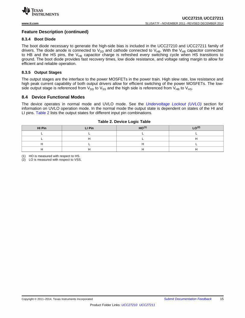
8.4 Device Functional ModesThe device operates in normal mode and UVLO mode. See the Undervoltage Lockout (UVLO) section forinformation on UVLO operation mode. In the normal mode the output state is dependent on states of the HI andLI pins. Table 2 lists the output states for different input pin combinations.
Table 2. Device Logic TableHI Pin LI Pin HO (1) LO (2)
L L L LL H L HH L H LH H H H

PWM
CONTROLLER
+12V
ISOLATION
AND
FEEDBACK
+100V
SECONDARY
SIDE
CIRCUIT
HI
CO
NT
RO
L
DRIVE
LO
DRIVE
HI
VDD
UCC27210
VSS
LI
HB
HO
HS
LO
16
UCC27210, UCC27211SLUSAT7F –NOVEMBER 2011–REVISED DECEMBER 2014 www.ti.com
Product Folder Links: UCC27210 UCC27211
Submit Documentation Feedback Copyright © 2011–2014, Texas Instruments Incorporated
9 Application and Implementation
NOTEInformation in the following applications sections is not part of the TI componentspecification, and TI does not warrant its accuracy or completeness. TI’s customers areresponsible for determining suitability of components for their purposes. Customers shouldvalidate and test their design implementation to confirm system functionality.
9.1 Application InformationTo effect fast switching of power devices and reduce associated switching power losses, a powerful gate driver isemployed between the PWM output of controllers and the gates of the power semiconductor devices. Also, gatedrivers are indispensable when it is impossible for the PWM controller to directly drive the gates of the switchingdevices. With the advent of digital power, this situation will be often encountered because the PWM signal fromthe digital controller is often a 3.3-V logic signal which cannot effectively turn on a power switch. Level shiftingcircuitry is needed to boost the 3.3-V signal to the gate-drive voltage (such as 12 V) in order to fully turn on thepower device and minimize conduction losses. Traditional buffer drive circuits based on NPN/PNP bipolartransistors in totem-pole arrangement, being emitter follower configurations, prove inadequate with digital powerbecause they lack level-shifting capability. Gate drivers effectively combine both the level-shifting and buffer-drivefunctions. Gate drivers also find other needs such as minimizing the effect of high-frequency switching noise bylocating the high-current driver physically close to the power switch, driving gate-drive transformers andcontrolling floating power-device gates, reducing power dissipation and thermal stress in controllers by movinggate charge power losses from the controller into the driver.
Finally, emerging wide band-gap power device technologies such as GaN based switches, which are capable ofsupporting very high switching frequency operation, are driving very special requirements in terms of gate drivecapability. These requirements include operation at low VDD voltages (5 V or lower), low propagation delays andavailability in compact, low-inductance packages with good thermal capability. In summary gate-driver devicesare extremely important components in switching power, combining benefits of high-performance, low-costcomponent count and board-space reduction as well as simplified system design.
9.2 Typical Application
Figure 19. Typical Application Diagram: UCC27210

PWM
CONTROLLER
+12V
+100V SECONDARY
SIDE
CIRCUIT
HI
CO
NT
RO
L
DRIVE
LO
DRIVE
HI
VDD
UCC27211
VSS
LI
HB
HO
HS
LO
+12V
HI
CO
NT
RO
L
DRIVE
LO
DRIVE
HI
VDD
UCC27211
LI
HB
HO
HS
LO
+100V
17
UCC27210, UCC27211www.ti.com SLUSAT7F –NOVEMBER 2011–REVISED DECEMBER 2014
Product Folder Links: UCC27210 UCC27211
Submit Documentation FeedbackCopyright © 2011–2014, Texas Instruments Incorporated
Typical Application (continued)
Figure 20. Typical Application Diagram: UCC27211
9.2.1 Design Requirements
Table 3. Design SpecificationsDESIGN PARAMETER EXAMPLE VALUE
Supply voltage, VDD 12 VVoltage on HS, VHS 0 V to 100 VVoltage on HB, VHB 12 V to 112 V
Output current rating, IO –4 A to 4 AOperating frequency 500 kHz

18
UCC27210, UCC27211SLUSAT7F –NOVEMBER 2011–REVISED DECEMBER 2014 www.ti.com
Product Folder Links: UCC27210 UCC27211
Submit Documentation Feedback Copyright © 2011–2014, Texas Instruments Incorporated
9.2.2 Detailed Design Procedure
9.2.2.1 Input Threshold TypeThe UCC27210 and UCC27211 have an input maximum voltage range from –10 V to 20 V. This increasedrobustness means that both parts can be directly interfaced to gate drive transformers. The UCC27210 featurespseudo CMOS compatible inputs and UCC27211 features TTL compatible input threshold logic, with widehysteresis. The threshold voltage levels are low voltage and independent of the VDD supply voltage, whichallows compatibility with both logic-level input signals from microcontrollers as well as higher-voltage inputsignals from analog controllers. See the Electrical Characteristics table for the actual input threshold voltagelevels and hysteresis specifications for the UCC27210 and UCC27211 devices.
9.2.2.2 VDD Bias Supply VoltageThe bias supply voltage to be applied to the VDD pin of the device should never exceed the values listed in theRecommended Operating Conditions table. However, different power switches demand different voltage levels tobe applied at the gate terminals for effective turnon and turnoff. With certain power switches, a positive gatevoltage may be required for turnon and a negative gate voltage may be required for turnoff, in which case theVDD bias supply equals the voltage differential. With a wide operating range from 8 V to 17 V, the UCC27210and UCC27211 devices can be used to drive a variety of power switches, such as Si MOSFETs, IGBTs, andwide-bandgap power semiconductors (such as GaN, certain types of which allow no higher than 6 V to beapplied to the gate terminals).
9.2.2.3 Peak Source and Sink CurrentsGenerally, the switching speed of the power switch during turnon and turnoff should be as fast as possible inorder to minimize switching power losses. The gate driver device must be able to provide the required peakcurrent for achieving the targeted switching speeds with the targeted power MOSFET. The system requirementfor the switching speed is typically described in terms of the slew rate of the drain-to-source voltage of the powerMOSFET (such as dVDS/dt). For example, the system requirement might state that a SPP20N60C3 powerMOSFET must be turned-on with a dVDS/dt of 20V/ns or higher with a DC bus voltage of 400 V in a continuous-conduction-mode (CCM) boost PFC-converter application. This type of application is an inductive hard-switchingapplication and reducing switching power losses is critical. This requirement means that the entire drain-to-source voltage swing during power MOSFET turnon event (from 400 V in the OFF state to VDS(on) in on state)must be completed in approximately 20 ns or less. When the drain-to-source voltage swing occurs, the Millercharge of the power MOSFET (QGD parameter in SPP20N60C3 data sheet is 33 nC typical) is supplied by thepeak current of gate driver. According to power MOSFET inductive switching mechanism, the gate-to-sourcevoltage of the power MOSFET at this time is the Miller plateau voltage, which is typically a few volts higher thanthe threshold voltage of the power MOSFET, VGS(TH).
To achieve the targeted dVDS/dt, the gate driver must be capable of providing the QGD charge in 20 ns or less. Inother words a peak current of 1.65 A (= 33 nC / 20 ns) or higher must be provided by the gate driver. TheUCC27210 and UCC27211 gate driver is capable of providing 4-A peak sourcing current which clearly exceedsthe design requirement and has the capability to meet the switching speed needed. The 2.4x overdrive capabilityprovides an extra margin against part-to-part variations in the QGD parameter of the power MOSFET along withadditional flexibility to insert external gate resistors and fine tune the switching speed for efficiency versus EMIoptimizations. However, in practical designs the parasitic trace inductance in the gate drive circuit of the PCB willhave a definitive role to play on the power MOSFET switching speed. The effect of this trace inductance is tolimit the dI/dt of the output current pulse of the gate driver. In order to illustrate this, consider output current pulsewaveform from the gate driver to be approximated to a triangular profile, where the area under the triangle (½×IPEAK × time) would equal the total gate charge of the power MOSFET (QG parameter in SPP20N60C3 powerMOSFET datasheet = 87 nC typical). If the parasitic trace inductance limits the dI/dt then a situation may occur inwhich the full peak current capability of the gate driver is not fully achieved in the time required to deliver the QGrequired for the power MOSFET switching. In other words the time parameter in the equation would dominateand the IPEAK value of the current pulse would be much less than the true peak current capability of the device,while the required QG is still delivered. Because of this, the desired switching speed may not be realized, evenwhen theoretical calculations indicate the gate driver is capable of achieving the targeted switching speed. Thus,placing the gate driver device very close to the power MOSFET and designing a tight gate drive-loop withminimal PCB trace inductance is important to realize the full peak-current capability of the gate driver.
19
UCC27210, UCC27211www.ti.com SLUSAT7F –NOVEMBER 2011–REVISED DECEMBER 2014
Product Folder Links: UCC27210 UCC27211
Submit Documentation FeedbackCopyright © 2011–2014, Texas Instruments Incorporated
9.2.2.4 Propagation DelayThe acceptable propagation delay from the gate driver is dependent on the switching frequency at which it isused and the acceptable level of pulse distortion to the system. The UCC27210 features 21 ns and theUCC27211 features 17 ns (typical) propagation delays which ensures very little pulse distortion and allowsoperation at very high-frequencies. See the Electrical Characteristics table for the propagation and switchingcharacteristics of the UCC27210 and UCC27211 devices.
9.2.2.5 Power DissipationPower dissipation of the gate driver has two portions as shown in Equation 1.
PDISS = PDC + PSW (1)
The DC portion of the power dissipation is PDC = IQ x VDD where IQ is the quiescent current for the driver. Thequiescent current is the current consumed by the device to bias all internal circuits such as input stage, referencevoltage, logic circuits, protections, and also any current associated with switching of internal devices when thedriver output changes state (such as charging and discharging of parasitic capacitances, parasitic shoot-through,and so forth). The UCC27210 and UCC27211 features very low quiescent currents (less than 0.17 mA, refer tothe Electrical Characteristics table and contain internal logic to eliminate any shoot-through in the output driverstage. Thus the effect of the PDC on the total power dissipation within the gate driver can be safely assumed tobe negligible. The power dissipated in the gate-driver package during switching (PSW) depends on the followingfactors:• Gate charge required of the power device (usually a function of the drive voltage VG, which is very close to
input bias supply voltage VDD)• Switching frequency• Use of external gate resistors. When a driver device is tested with a discrete, capacitive load calculating the
power that is required from the bias supply is fairly simple. The energy that must be transferred from the biassupply to charge the capacitor is given by Equation 2.
EG = ½CLOADVDD² fSW
where• CLOAD is load capacitor• VDD is bias voltage feeding the driver (2)
There is an equal amount of energy dissipated when the capacitor is charged. This leads to a total power lossgiven by Equation 3.
PG = CLOADVDD² fSW
where• fSW is the switching frequency (3)
The switching load presented by a power MOSFET/IGBT is converted to an equivalent capacitance by examiningthe gate charge required to switch the device. This gate charge includes the effects of the input capacitance plusthe added charge needed to swing the drain voltage of the power device as it switches between the ON and OFFstates. Most manufacturers provide specifications of typical and maximum gate charge, in nC, to switch thedevice under specified conditions. Using the gate charge Qg, determine the power that must be dissipated whencharging a capacitor which is calculated using the equation QG = CLOAD x VDD to provide Equation 4 for power.
PG = CLOADVDD² fSW = QGVDDfSW (4)
This power PG is dissipated in the resistive elements of the circuit when the MOSFET/IGBT is being turned on oroff. Half of the total power is dissipated when the load capacitor is charged during turnon, and the other half isdissipated when the load capacitor is discharged during turnoff. When no external gate resistor is employedbetween the driver and MOSFET/IGBT, this power is completely dissipated inside the driver package. With theuse of external gate-drive resistors, the power dissipation is shared between the internal resistance of driver andexternal gate resistor.

20
UCC27210, UCC27211SLUSAT7F –NOVEMBER 2011–REVISED DECEMBER 2014 www.ti.com
Product Folder Links: UCC27210 UCC27211
Submit Documentation Feedback Copyright © 2011–2014, Texas Instruments Incorporated
9.2.3 Application Curves
Figure 21. Negative 10-V Input Figure 22. Step Input
Figure 23. Symmetrical UVLO

21
UCC27210, UCC27211www.ti.com SLUSAT7F –NOVEMBER 2011–REVISED DECEMBER 2014
Product Folder Links: UCC27210 UCC27211
Submit Documentation FeedbackCopyright © 2011–2014, Texas Instruments Incorporated
10 Power Supply RecommendationsThe bias supply voltage range for which the UCC27210 and UCC27211 device is rated to operate is from 8 V to17 V. The lower end of this range is governed by the internal undervoltage-lockout (UVLO) protection feature onthe VDD pin supply circuit blocks. Whenever the driver is in UVLO condition when the VDD pin voltage is belowthe V(ON) supply start threshold, this feature holds the output low, regardless of the status of the inputs. Theupper end of this range is driven by the 20-V absolute maximum voltage rating of the VDD pin of the device(which is a stress rating). Keeping a 3-V margin to allow for transient voltage spikes, the maximumrecommended voltage for the VDD pin is 17 V. The UVLO protection feature also involves a hysteresis function.This means that when the VDD pin bias voltage has exceeded the threshold voltage and device begins tooperate, and if the voltage drops, then the device continues to deliver normal functionality unless the voltagedrop exceeds the hysteresis specification VDD(hys).Therefore, ensuring that, while operating at or near the 8-Vrange, the voltage ripple on the auxiliary power supply output is smaller than the hysteresis specification of thedevice is important to avoid triggering device shutdown. During system shutdown, the device operation continuesuntil the VDD pin voltage has dropped below the V(OFF) threshold which must be accounted for while evaluatingsystem shutdown timing design requirements. Likewise, at system startup, the device does not begin operationuntil the VDD pin voltage has exceeded above the V(ON) threshold. The quiescent current consumed by theinternal circuit blocks of the device is supplied through the VDD pin. Although this fact is well known, recognizingthat the charge for source current pulses delivered by the HO pin is also supplied through the same VDD pin isimportant. As a result, every time a current is sourced out of the HO pin a corresponding current pulse isdelivered into the device through the VDD pin. Thus ensuring that a local bypass capacitor is provided betweenthe VDD and GND pins and located as close to the device as possible for the purpose of decoupling is important.A low ESR, ceramic surface mount capacitor is a must. TI recommends using a capacitor in the range 0.22 uF to4.7 uF between VDD and GND. In a similar manner, the current pulses delivered by the LO pin are sourced fromthe HB pin. Therefore a 0.022-uF to 0.1-uF local decoupling capacitor is recommended between the HB and HSpins.
11 Layout
11.1 Layout GuidelinesTo improve the switching characteristics and efficiency of a design, the following layout rules should be followed.• Locate the driver as close as possible to the MOSFETs.• Locate the VDD-VSS and VHB-VHS (bootstrap) capacitors as close as possible to the device (see Figure 24).• Pay close attention to the GND trace. Use the thermal pad of the DDA and DRM package as GND by
connecting it to the VSS pin (GND). The GND trace from the driver goes directly to the source of theMOSFET but should not be in the high current path of the MOSFET(S) drain or source current.
• Use similar rules for the HS node as for GND for the high-side driver.• For systems using multiple UCC27210 and UCC27211 devices we recommend that dedicated decoupling
capacitors be located at VDD-VSS for each device.• Care should be taken to avoid VDD traces being close to LO, HS, and HO signals.• Use wide traces for LO and HO closely following the associated GND or HS traces. 60 to 100-mils width is
preferable where possible.• Use as least two or more vias if the driver outputs or SW node must be routed from one layer to another. For
GND the number of vias must be a consideration of the thermal pad requirements as well as parasiticinductance.
• Avoid LI and HI (driver input) going close to the HS node or any other high dV/dT traces that can inducesignificant noise into the relatively high impedance leads.
Keep in mind that a poor layout can cause a significant drop in efficiency or system malfunction versus a goodPCB layout and can even lead to decreased reliability of the whole system.

22
UCC27210, UCC27211SLUSAT7F –NOVEMBER 2011–REVISED DECEMBER 2014 www.ti.com
Product Folder Links: UCC27210 UCC27211
Submit Documentation Feedback Copyright © 2011–2014, Texas Instruments Incorporated
11.2 Layout Example
Figure 24. UCC27210/11 Component Placement
11.3 Thermal ConsiderationsThe useful range of a driver is greatly affected by the drive-power requirements of the load and the thermalcharacteristics of the package. In order for a gate driver to be useful over a particular temperature range thepackage must allow for the efficient removal of the heat produced while keeping the junction temperature withinrated limits. The thermal metrics for the driver package is listed in Device Functional Modes. For detailedinformation regarding the table, please refer to the Application Note from Texas Instruments entitled IC PackageThermal Metrics (SPRA953). The UCC27210 and UCC27211 devices are offered in SOIC (8), PowerPad (8),WSON (10) or VSON (8). The Thermal Information section lists the thermal performance metrics related to SOT-23 package.

23
UCC27210, UCC27211www.ti.com SLUSAT7F –NOVEMBER 2011–REVISED DECEMBER 2014
Product Folder Links: UCC27210 UCC27211
Submit Documentation FeedbackCopyright © 2011–2014, Texas Instruments Incorporated
12 Device and Documentation Support
12.1 Documentation Support
12.1.1 Related DocumentationThese references and links to additional information may be found at www.ti.com• Additional layout guidelines for PCB land patterns may be found in, QFN/SON PCB Attachment, Application
Brief (SLUA271)• Additional thermal performance guidelines may be found in, PowerPAD™ Thermally Enhanced Package
Application Report, Application Report (SLMA002)• Additional thermal performance guidelines may be found in, PowerPAD™ Made Easy, Application Report
(SLMA004)
12.2 Related LinksThe table below lists quick access links. Categories include technical documents, support and communityresources, tools and software, and quick access to sample or buy.
Table 4. Related Links
PARTS PRODUCT FOLDER SAMPLE & BUY TECHNICALDOCUMENTS
TOOLS &SOFTWARE
SUPPORT &COMMUNITY
UCC27210 Click here Click here Click here Click here Click hereUCC27211 Click here Click here Click here Click here Click here
12.3 TrademarksPowerPAD is a trademark of Texas Instruments.All other trademarks are the property of their respective owners.
12.4 Electrostatic Discharge CautionThese devices have limited built-in ESD protection. The leads should be shorted together or the device placed in conductive foamduring storage or handling to prevent electrostatic damage to the MOS gates.
12.5 GlossarySLYZ022 — TI Glossary.
This glossary lists and explains terms, acronyms, and definitions.
13 Mechanical, Packaging, and Orderable InformationThe following pages include mechanical, packaging, and orderable information. This information is the mostcurrent data available for the designated devices. This data is subject to change without notice and revision ofthis document. For browser-based versions of this data sheet, refer to the left-hand navigation.

PACKAGE OPTION ADDENDUM
www.ti.com 22-Dec-2017
Addendum-Page 1
PACKAGING INFORMATION
Orderable Device Status(1)
Package Type PackageDrawing
Pins PackageQty
Eco Plan(2)
Lead/Ball Finish(6)
MSL Peak Temp(3)
Op Temp (°C) Device Marking(4/5)
Samples
UCC27210D ACTIVE SOIC D 8 75 Green (RoHS& no Sb/Br)
CU NIPDAU Level-1-260C-UNLIM -40 to 140 27210
UCC27210DDA ACTIVE SO PowerPAD DDA 8 75 Green (RoHS& no Sb/Br)
CU NIPDAUAG Level-1-260C-UNLIM -40 to 140 27210
UCC27210DDAR ACTIVE SO PowerPAD DDA 8 2500 Green (RoHS& no Sb/Br)
CU NIPDAUAG Level-1-260C-UNLIM -40 to 140 27210
UCC27210DPRR ACTIVE WSON DPR 10 3000 Green (RoHS& no Sb/Br)
CU NIPDAU Level-2-260C-1 YEAR -40 to 140 UCC27210
UCC27210DPRT ACTIVE WSON DPR 10 250 Green (RoHS& no Sb/Br)
CU NIPDAU Level-2-260C-1 YEAR -40 to 140 UCC27210
UCC27210DR ACTIVE SOIC D 8 2500 Green (RoHS& no Sb/Br)
CU NIPDAU Level-1-260C-UNLIM -40 to 140 27210
UCC27210DRMR ACTIVE VSON DRM 8 3000 Green (RoHS& no Sb/Br)
CU NIPDAUAG Level-1-260C-UNLIM -40 to 140 27210
UCC27210DRMT ACTIVE VSON DRM 8 250 Green (RoHS& no Sb/Br)
CU NIPDAUAG Level-1-260C-UNLIM -40 to 140 27210
UCC27211D ACTIVE SOIC D 8 75 Green (RoHS& no Sb/Br)
CU NIPDAU Level-1-260C-UNLIM -40 to 140 27211
UCC27211DDA ACTIVE SO PowerPAD DDA 8 75 Green (RoHS& no Sb/Br)
CU NIPDAUAG Level-1-260C-UNLIM -40 to 140 27211
UCC27211DDAR ACTIVE SO PowerPAD DDA 8 2500 Green (RoHS& no Sb/Br)
CU NIPDAUAG Level-1-260C-UNLIM -40 to 140 27211
UCC27211DPRR ACTIVE WSON DPR 10 3000 Green (RoHS& no Sb/Br)
CU NIPDAU Level-2-260C-1 YEAR -40 to 140 UCC27211
UCC27211DPRT ACTIVE WSON DPR 10 250 Green (RoHS& no Sb/Br)
CU NIPDAU Level-2-260C-1 YEAR -40 to 140 UCC27211
UCC27211DR ACTIVE SOIC D 8 2500 Green (RoHS& no Sb/Br)
CU NIPDAU Level-1-260C-UNLIM -40 to 140 27211
UCC27211DRMR ACTIVE VSON DRM 8 3000 Green (RoHS& no Sb/Br)
CU NIPDAUAG Level-1-260C-UNLIM -40 to 140 27211
UCC27211DRMT ACTIVE VSON DRM 8 250 Green (RoHS& no Sb/Br)
CU NIPDAUAG Level-1-260C-UNLIM -40 to 140 27211
(1) The marketing status values are defined as follows:ACTIVE: Product device recommended for new designs.

PACKAGE OPTION ADDENDUM
www.ti.com 22-Dec-2017
Addendum-Page 2
LIFEBUY: TI has announced that the device will be discontinued, and a lifetime-buy period is in effect.NRND: Not recommended for new designs. Device is in production to support existing customers, but TI does not recommend using this part in a new design.PREVIEW: Device has been announced but is not in production. Samples may or may not be available.OBSOLETE: TI has discontinued the production of the device.
(2) RoHS: TI defines "RoHS" to mean semiconductor products that are compliant with the current EU RoHS requirements for all 10 RoHS substances, including the requirement that RoHS substancedo not exceed 0.1% by weight in homogeneous materials. Where designed to be soldered at high temperatures, "RoHS" products are suitable for use in specified lead-free processes. TI mayreference these types of products as "Pb-Free".RoHS Exempt: TI defines "RoHS Exempt" to mean products that contain lead but are compliant with EU RoHS pursuant to a specific EU RoHS exemption.Green: TI defines "Green" to mean the content of Chlorine (Cl) and Bromine (Br) based flame retardants meet JS709B low halogen requirements of <=1000ppm threshold. Antimony trioxide basedflame retardants must also meet the <=1000ppm threshold requirement.
(3) MSL, Peak Temp. - The Moisture Sensitivity Level rating according to the JEDEC industry standard classifications, and peak solder temperature.
(4) There may be additional marking, which relates to the logo, the lot trace code information, or the environmental category on the device.
(5) Multiple Device Markings will be inside parentheses. Only one Device Marking contained in parentheses and separated by a "~" will appear on a device. If a line is indented then it is a continuationof the previous line and the two combined represent the entire Device Marking for that device.
(6) Lead/Ball Finish - Orderable Devices may have multiple material finish options. Finish options are separated by a vertical ruled line. Lead/Ball Finish values may wrap to two lines if the finishvalue exceeds the maximum column width.
Important Information and Disclaimer:The information provided on this page represents TI's knowledge and belief as of the date that it is provided. TI bases its knowledge and belief on informationprovided by third parties, and makes no representation or warranty as to the accuracy of such information. Efforts are underway to better integrate information from third parties. TI has taken andcontinues to take reasonable steps to provide representative and accurate information but may not have conducted destructive testing or chemical analysis on incoming materials and chemicals.TI and TI suppliers consider certain information to be proprietary, and thus CAS numbers and other limited information may not be available for release.
In no event shall TI's liability arising out of such information exceed the total purchase price of the TI part(s) at issue in this document sold by TI to Customer on an annual basis.
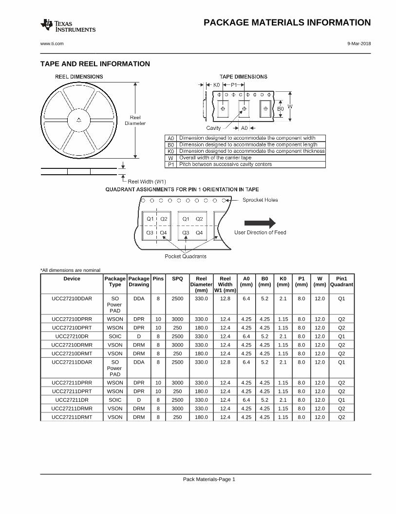
TAPE AND REEL INFORMATION
*All dimensions are nominal
Device PackageType
PackageDrawing
Pins SPQ ReelDiameter
(mm)
ReelWidth
W1 (mm)
A0(mm)
B0(mm)
K0(mm)
P1(mm)
W(mm)
Pin1Quadrant
UCC27210DDAR SOPower PAD
DDA 8 2500 330.0 12.8 6.4 5.2 2.1 8.0 12.0 Q1
UCC27210DPRR WSON DPR 10 3000 330.0 12.4 4.25 4.25 1.15 8.0 12.0 Q2
UCC27210DPRT WSON DPR 10 250 180.0 12.4 4.25 4.25 1.15 8.0 12.0 Q2
UCC27210DR SOIC D 8 2500 330.0 12.4 6.4 5.2 2.1 8.0 12.0 Q1
UCC27210DRMR VSON DRM 8 3000 330.0 12.4 4.25 4.25 1.15 8.0 12.0 Q2
UCC27210DRMT VSON DRM 8 250 180.0 12.4 4.25 4.25 1.15 8.0 12.0 Q2
UCC27211DDAR SOPower PAD
DDA 8 2500 330.0 12.8 6.4 5.2 2.1 8.0 12.0 Q1
UCC27211DPRR WSON DPR 10 3000 330.0 12.4 4.25 4.25 1.15 8.0 12.0 Q2
UCC27211DPRT WSON DPR 10 250 180.0 12.4 4.25 4.25 1.15 8.0 12.0 Q2
UCC27211DR SOIC D 8 2500 330.0 12.4 6.4 5.2 2.1 8.0 12.0 Q1
UCC27211DRMR VSON DRM 8 3000 330.0 12.4 4.25 4.25 1.15 8.0 12.0 Q2
UCC27211DRMT VSON DRM 8 250 180.0 12.4 4.25 4.25 1.15 8.0 12.0 Q2
PACKAGE MATERIALS INFORMATION
www.ti.com 9-Mar-2018
Pack Materials-Page 1

*All dimensions are nominal
Device Package Type Package Drawing Pins SPQ Length (mm) Width (mm) Height (mm)
UCC27210DDAR SO PowerPAD DDA 8 2500 366.0 364.0 50.0
UCC27210DPRR WSON DPR 10 3000 367.0 367.0 35.0
UCC27210DPRT WSON DPR 10 250 210.0 185.0 35.0
UCC27210DR SOIC D 8 2500 367.0 367.0 35.0
UCC27210DRMR VSON DRM 8 3000 367.0 367.0 35.0
UCC27210DRMT VSON DRM 8 250 210.0 185.0 35.0
UCC27211DDAR SO PowerPAD DDA 8 2500 366.0 364.0 50.0
UCC27211DPRR WSON DPR 10 3000 367.0 367.0 35.0
UCC27211DPRT WSON DPR 10 250 210.0 185.0 35.0
UCC27211DR SOIC D 8 2500 367.0 367.0 35.0
UCC27211DRMR VSON DRM 8 3000 367.0 367.0 35.0
UCC27211DRMT VSON DRM 8 250 210.0 185.0 35.0
PACKAGE MATERIALS INFORMATION
www.ti.com 9-Mar-2018
Pack Materials-Page 2


IMPORTANT NOTICE
Texas Instruments Incorporated (TI) reserves the right to make corrections, enhancements, improvements and other changes to itssemiconductor products and services per JESD46, latest issue, and to discontinue any product or service per JESD48, latest issue. Buyersshould obtain the latest relevant information before placing orders and should verify that such information is current and complete.TI’s published terms of sale for semiconductor products (http://www.ti.com/sc/docs/stdterms.htm) apply to the sale of packaged integratedcircuit products that TI has qualified and released to market. Additional terms may apply to the use or sale of other types of TI products andservices.Reproduction of significant portions of TI information in TI data sheets is permissible only if reproduction is without alteration and isaccompanied by all associated warranties, conditions, limitations, and notices. TI is not responsible or liable for such reproduceddocumentation. Information of third parties may be subject to additional restrictions. Resale of TI products or services with statementsdifferent from or beyond the parameters stated by TI for that product or service voids all express and any implied warranties for theassociated TI product or service and is an unfair and deceptive business practice. TI is not responsible or liable for any such statements.Buyers and others who are developing systems that incorporate TI products (collectively, “Designers”) understand and agree that Designersremain responsible for using their independent analysis, evaluation and judgment in designing their applications and that Designers havefull and exclusive responsibility to assure the safety of Designers' applications and compliance of their applications (and of all TI productsused in or for Designers’ applications) with all applicable regulations, laws and other applicable requirements. Designer represents that, withrespect to their applications, Designer has all the necessary expertise to create and implement safeguards that (1) anticipate dangerousconsequences of failures, (2) monitor failures and their consequences, and (3) lessen the likelihood of failures that might cause harm andtake appropriate actions. Designer agrees that prior to using or distributing any applications that include TI products, Designer willthoroughly test such applications and the functionality of such TI products as used in such applications.TI’s provision of technical, application or other design advice, quality characterization, reliability data or other services or information,including, but not limited to, reference designs and materials relating to evaluation modules, (collectively, “TI Resources”) are intended toassist designers who are developing applications that incorporate TI products; by downloading, accessing or using TI Resources in anyway, Designer (individually or, if Designer is acting on behalf of a company, Designer’s company) agrees to use any particular TI Resourcesolely for this purpose and subject to the terms of this Notice.TI’s provision of TI Resources does not expand or otherwise alter TI’s applicable published warranties or warranty disclaimers for TIproducts, and no additional obligations or liabilities arise from TI providing such TI Resources. TI reserves the right to make corrections,enhancements, improvements and other changes to its TI Resources. TI has not conducted any testing other than that specificallydescribed in the published documentation for a particular TI Resource.Designer is authorized to use, copy and modify any individual TI Resource only in connection with the development of applications thatinclude the TI product(s) identified in such TI Resource. NO OTHER LICENSE, EXPRESS OR IMPLIED, BY ESTOPPEL OR OTHERWISETO ANY OTHER TI INTELLECTUAL PROPERTY RIGHT, AND NO LICENSE TO ANY TECHNOLOGY OR INTELLECTUAL PROPERTYRIGHT OF TI OR ANY THIRD PARTY IS GRANTED HEREIN, including but not limited to any patent right, copyright, mask work right, orother intellectual property right relating to any combination, machine, or process in which TI products or services are used. Informationregarding or referencing third-party products or services does not constitute a license to use such products or services, or a warranty orendorsement thereof. Use of TI Resources may require a license from a third party under the patents or other intellectual property of thethird party, or a license from TI under the patents or other intellectual property of TI.TI RESOURCES ARE PROVIDED “AS IS” AND WITH ALL FAULTS. TI DISCLAIMS ALL OTHER WARRANTIES ORREPRESENTATIONS, EXPRESS OR IMPLIED, REGARDING RESOURCES OR USE THEREOF, INCLUDING BUT NOT LIMITED TOACCURACY OR COMPLETENESS, TITLE, ANY EPIDEMIC FAILURE WARRANTY AND ANY IMPLIED WARRANTIES OFMERCHANTABILITY, FITNESS FOR A PARTICULAR PURPOSE, AND NON-INFRINGEMENT OF ANY THIRD PARTY INTELLECTUALPROPERTY RIGHTS. TI SHALL NOT BE LIABLE FOR AND SHALL NOT DEFEND OR INDEMNIFY DESIGNER AGAINST ANY CLAIM,INCLUDING BUT NOT LIMITED TO ANY INFRINGEMENT CLAIM THAT RELATES TO OR IS BASED ON ANY COMBINATION OFPRODUCTS EVEN IF DESCRIBED IN TI RESOURCES OR OTHERWISE. IN NO EVENT SHALL TI BE LIABLE FOR ANY ACTUAL,DIRECT, SPECIAL, COLLATERAL, INDIRECT, PUNITIVE, INCIDENTAL, CONSEQUENTIAL OR EXEMPLARY DAMAGES INCONNECTION WITH OR ARISING OUT OF TI RESOURCES OR USE THEREOF, AND REGARDLESS OF WHETHER TI HAS BEENADVISED OF THE POSSIBILITY OF SUCH DAMAGES.Unless TI has explicitly designated an individual product as meeting the requirements of a particular industry standard (e.g., ISO/TS 16949and ISO 26262), TI is not responsible for any failure to meet such industry standard requirements.Where TI specifically promotes products as facilitating functional safety or as compliant with industry functional safety standards, suchproducts are intended to help enable customers to design and create their own applications that meet applicable functional safety standardsand requirements. Using products in an application does not by itself establish any safety features in the application. Designers mustensure compliance with safety-related requirements and standards applicable to their applications. Designer may not use any TI products inlife-critical medical equipment unless authorized officers of the parties have executed a special contract specifically governing such use.Life-critical medical equipment is medical equipment where failure of such equipment would cause serious bodily injury or death (e.g., lifesupport, pacemakers, defibrillators, heart pumps, neurostimulators, and implantables). Such equipment includes, without limitation, allmedical devices identified by the U.S. Food and Drug Administration as Class III devices and equivalent classifications outside the U.S.TI may expressly designate certain products as completing a particular qualification (e.g., Q100, Military Grade, or Enhanced Product).Designers agree that it has the necessary expertise to select the product with the appropriate qualification designation for their applicationsand that proper product selection is at Designers’ own risk. Designers are solely responsible for compliance with all legal and regulatoryrequirements in connection with such selection.Designer will fully indemnify TI and its representatives against any damages, costs, losses, and/or liabilities arising out of Designer’s non-compliance with the terms and provisions of this Notice.
Mailing Address: Texas Instruments, Post Office Box 655303, Dallas, Texas 75265Copyright © 2018, Texas Instruments Incorporated