12. Recommended Design Practices
38
QII51006-13.1.0 © 2013 Altera Corporation. All rights reserved. ALTERA, ARRIA, CYCLONE, HARDCOPY, MAX, MEGACORE, NIOS, QUARTUS and STRATIX words and logos are trademarks of Altera Corporation and registered in the U.S. Patent and Trademark Office and in other countries. All other words and logos identified as trademarks or service marks are the property of their respective holders as described at www.altera.com/common/legal.html. Altera warrants performance of its semiconductor products to current specifications in accordance with Altera's standard warranty, but reserves the right to make changes to any products and services at any time without notice. Altera assumes no responsibility or liability arising out of the application or use of any information, product, or service described herein except as expressly agreed to in writing by Altera. Altera customers are advised to obtain the latest version of device specifications before relying on any published information and before placing orders for products or services. Quartus II Handbook Version 13.1 Volume 1: Design and Synthesis November 2013 Feedback Subscribe Twitter ISO 9001:2008 Registered 12. Recommended Design Practices This chapter provides design recommendations for Altera ® devices and describes the Quartus ® II Design Assistant, which helps you check your design for violations of Altera’s design recommendations. Current FPGA applications have reached the complexity and performance requirements of ASICs. In the development of complex system designs, good design practices have an enormous impact on the timing performance, logic utilization, and system reliability of a device. Well-coded designs behave in a predictable and reliable manner even when retargeted to different families or speed grades. Good design practices also aid in successful design migration between FPGA and ASIC implementations for prototyping and production. For optimal performance, reliability, and faster time-to-market when designing with Altera devices, you should adhere to the following guidelines: ■ Understand the impact of synchronous design practices ■ Follow recommended design techniques, including hierarchical design partitioning, and timing closure guidelines ■ Take advantage of the architectural features in the targeted device This chapter contains the following sections: ■ “Synchronous FPGA Design Practices” on page 12–2 ■ “Design Guidelines” on page 12–4 ■ “Optimizing for Physical Implementation and Timing Closure” on page 12–12 ■ “Checking Design Violations” on page 12–16 ■ “Targeting Clock and Register-Control Architectural Features” on page 12–23 ■ “Targeting Embedded RAM Architectural Features” on page 12–35 f For specific HDL coding examples and recommendations, including coding guidelines for targeting dedicated device hardware, such as memory and digital signal processing (DSP) blocks, refer to the Recommended HDL Coding Styles chapter in volume 1 of the Quartus II Handbook. For information about partitioning a hierarchical design for incremental compilation, refer to the Quartus II Incremental Compilation for Hierarchical and Team-Based Design chapter in volume 1 of the Quartus II Handbook. November 2013 QII51006-13.1.0
Transcript of 12. Recommended Design Practices

QII51006-13.1.0
© 2013 Altera Corporation. All rights reserved. ALTERA, ARRIare trademarks of Altera Corporation and registered in the U.Strademarks or service marks are the property of their respectivsemiconductor products to current specifications in accordanceservices at any time without notice. Altera assumes no responsdescribed herein except as expressly agreed to in writing by Alon any published information and before placing orders for pr
Quartus II Handbook Version 13.1Volume 1: Design and SynthesisNovember 2013
November 2013QII51006-13.1.0
12. Recommended Design Practices
This chapter provides design recommendations for Altera® devices and describes theQuartus® II Design Assistant, which helps you check your design for violations ofAltera’s design recommendations.
Current FPGA applications have reached the complexity and performancerequirements of ASICs. In the development of complex system designs, good designpractices have an enormous impact on the timing performance, logic utilization, andsystem reliability of a device. Well-coded designs behave in a predictable and reliablemanner even when retargeted to different families or speed grades. Good designpractices also aid in successful design migration between FPGA and ASICimplementations for prototyping and production.
For optimal performance, reliability, and faster time-to-market when designing withAltera devices, you should adhere to the following guidelines:
■ Understand the impact of synchronous design practices
■ Follow recommended design techniques, including hierarchical designpartitioning, and timing closure guidelines
■ Take advantage of the architectural features in the targeted device
This chapter contains the following sections:
■ “Synchronous FPGA Design Practices” on page 12–2
■ “Design Guidelines” on page 12–4
■ “Optimizing for Physical Implementation and Timing Closure” on page 12–12
■ “Checking Design Violations” on page 12–16
■ “Targeting Clock and Register-Control Architectural Features” on page 12–23
■ “Targeting Embedded RAM Architectural Features” on page 12–35
f For specific HDL coding examples and recommendations, including codingguidelines for targeting dedicated device hardware, such as memory and digitalsignal processing (DSP) blocks, refer to the Recommended HDL Coding Styles chapter involume 1 of the Quartus II Handbook. For information about partitioning a hierarchicaldesign for incremental compilation, refer to the Quartus II Incremental Compilation forHierarchical and Team-Based Design chapter in volume 1 of the Quartus II Handbook.
A, CYCLONE, HARDCOPY, MAX, MEGACORE, NIOS, QUARTUS and STRATIX words and logos. Patent and Trademark Office and in other countries. All other words and logos identified ase holders as described at www.altera.com/common/legal.html. Altera warrants performance of itswith Altera's standard warranty, but reserves the right to make changes to any products and
ibility or liability arising out of the application or use of any information, product, or servicetera. Altera customers are advised to obtain the latest version of device specifications before relyingoducts or services.
Feedback SubscribeTwitter
ISO9001:2008Registered

12–2 Chapter 12: Recommended Design PracticesSynchronous FPGA Design Practices
Synchronous FPGA Design PracticesThe first step in good design methodology is to understand the implications of yourdesign practices and techniques. This section outlines the benefits of optimalsynchronous design practices and the hazards involved in other techniques. Goodsynchronous design practices can help you meet your design goals consistently.Problems with other design techniques can include reliance on propagation delays ina device, which can lead to race conditions, incomplete timing analysis, and possibleglitches.
In a synchronous design, some clock signals trigger every event. As long as youensure that all the timing requirements of the registers are met, a synchronous designbehaves in a predictable and reliable manner for all process, voltage, and temperature(PVT) conditions. You can easily target synchronous designs to different devicefamilies or speed grades.
Fundamentals of Synchronous DesignIn a synchronous design, the clock signal controls the activities of all inputs andoutputs. On every active edge of the clock (usually the rising edge), the data inputs ofregisters are sampled and transferred to outputs. Following an active clock edge, theoutputs of combinational logic feeding the data inputs of registers change values. Thischange triggers a period of instability due to propagation delays through the logic asthe signals go through several transitions and finally settle to new values. Changesthat occur on data inputs of registers do not affect the values of their outputs untilafter the next active clock edge.
Because the internal circuitry of registers isolates data outputs from inputs, instabilityin the combinational logic does not affect the operation of the design as long as youmeet the following timing requirements:
■ Before an active clock edge, you must ensure that the data input has been stablefor at least the setup time of the register.
■ After an active clock edge, you must ensure that the data input remains stable forat least the hold time of the register.
When you specify all of your clock frequencies and other timing requirements, theQuartus II TimeQuest Timing Analyzer reports actual hardware requirements for thesetup times (tSU) and hold times (tH) for every pin in your design. By meeting theseexternal pin requirements and following synchronous design techniques, you ensurethat you satisfy the setup and hold times for all registers in your device.
1 To meet setup and hold time requirements on all input pins, any inputs tocombinational logic that feed a register should have a synchronous relationship withthe clock of the register. If signals are asynchronous, you can register the signals at theinputs of the device to help prevent a violation of the required setup and hold times.
Quartus II Handbook Version 13.1 November 2013 Altera CorporationVolume 1: Design and Synthesis

Chapter 12: Recommended Design Practices 12–3Synchronous FPGA Design Practices
When you violate the setup or hold time of a register, you might oscillate the output,or set the output to an intermediate voltage level between the high and low levelscalled a metastable state. In this unstable state, small perturbations such as noise inpower rails can cause the register to assume either the high or low voltage level,resulting in an unpredictable valid state. Various undesirable effects can occur,including increased propagation delays and incorrect output states. In some cases, theoutput can even oscillate between the two valid states for a relatively long period oftime.
h For information about timing requirements and analysis in the Quartus II software,refer to About TimeQuest Timing Analysis in Quartus II Help.
Hazards of Asynchronous DesignIn the past, designers have often used asynchronous techniques such as ripplecounters or pulse generators in programmable logic device (PLD) designs, enablingthem to take “short cuts” to save device resources. Asynchronous design techniqueshave inherent problems such as relying on propagation delays in a device, which canvary with temperature and voltage fluctuations, resulting in incomplete timingconstraints and possible glitches and spikes.
Some asynchronous design structures rely on the relative propagation delays ofsignals to function correctly. In these cases, race conditions can arise where the orderof signal changes can affect the output of the logic. PLD designs can have varyingtiming delays, depending on how the design is placed and routed in the device witheach compilation. Therefore, it is almost impossible to determine the timing delayassociated with a particular block of logic ahead of time. As devices become faster dueto device process improvements, the delays in an asynchronous design may decrease,resulting in a design that does not function as expected. Specific examples areprovided in “Design Guidelines” on page 12–4. Relying on a particular delay alsomakes asynchronous designs difficult to migrate to different architectures, devices, orspeed grades.
The timing of asynchronous design structures is often difficult or impossible to modelwith timing assignments and constraints. If you do not have complete or accuratetiming constraints, the timing-driven algorithms used by your synthesis andplace-and-route tools may not be able to perform the best optimizations, and thereported results may not be complete.
Some asynchronous design structures can generate harmful glitches, which are pulsesthat are very short compared with clock periods. Most glitches are generated bycombinational logic. When the inputs of combinational logic change, the outputsexhibit several glitches before they settle to their new values. These glitches canpropagate through the combinational logic, leading to incorrect values on the outputsin asynchronous designs. In a synchronous design, glitches on the data inputs ofregisters are normal events that have no negative consequences because the data isnot processed until the clock edge.
November 2013 Altera Corporation Quartus II Handbook Version 13.1Volume 1: Design and Synthesis

12–4 Chapter 12: Recommended Design PracticesDesign Guidelines
Design GuidelinesWhen designing with HDL code, you should understand how a synthesis toolinterprets different HDL design techniques and what results to expect. Your designtechniques can affect logic utilization and timing performance, as well as the design’sreliability. This section describes basic design techniques that ensure optimalsynthesis results for designs targeted to Altera devices while avoiding severalcommon causes of unreliability and instability. Altera recommends that you designyour combinational logic carefully to avoid potential problems and pay attention toyour clocking schemes so that you can maintain synchronous functionality and avoidtiming problems.
Combinational Logic StructuresCombinational logic structures consist of logic functions that depend only on thecurrent state of the inputs. In Altera FPGAs, these functions are implemented in thelook-up tables (LUTs) with either logic elements (LEs) or adaptive logic modules(ALMs). For cases where combinational logic feeds registers, the register controlsignals can implement part of the logic function to save LUT resources. By followingthe recommendations in this section, you can improve the reliability of yourcombinational design.
Combinational LoopsCombinational loops are among the most common causes of instability andunreliability in digital designs. Combinational loops generally violate synchronousdesign principles by establishing a direct feedback loop that contains no registers. Youshould avoid combinational loops whenever possible. In a synchronous design,feedback loops should include registers. For example, a combinational loop occurswhen the left-hand side of an arithmetic expression also appears on the right-handside in HDL code. A combinational loop also occurs when you feed back the output ofa register to an asynchronous pin of the same register through combinational logic, asshown in Figure 12–1.
1 Use recovery and removal analysis to perform timing analysis on asynchronous ports,such as clear or reset in the Quartus II software.
h If you are using the TimeQuest Timing Analyzer, refer to Specifying Timing Constraintsand Exceptions (TimeQuest Timing Analyzer) in Quartus II Help for details about howTimeQuest analyzer performs recovery and removal analysis.
Figure 12–1. Combinational Loop Through Asynchronous Control Pin
D Q
CLRN
Logic
Quartus II Handbook Version 13.1 November 2013 Altera CorporationVolume 1: Design and Synthesis

Chapter 12: Recommended Design Practices 12–5Design Guidelines
Combinational loops are inherently high-risk design structures for the followingreasons:
■ Combinational loop behavior generally depends on relative propagation delaysthrough the logic involved in the loop. As discussed, propagation delays canchange, which means the behavior of the loop is unpredictable.
■ Combinational loops can cause endless computation loops in many design tools.Most tools break open combinational loops to process the design. The varioustools used in the design flow may open a given loop in a different manner,processing it in a way that is inconsistent with the original design intent.
LatchesA latch is a small circuit with combinational feedback that holds a value until a newvalue is assigned. You can implement latches with the Quartus II Text Editor or BlockEditor. It is common for mistakes in HDL code to cause unintended latch inference;Quartus II Synthesis issues a warning message if this occurs.
Unlike other technologies, a latch in FPGA architecture is not significantly smallerthan a register. The architecture is not optimized for latch implementation and latchesgenerally have slower timing performance compared to equivalent registeredcircuitry.
Latches have a transparent mode in which data flows continuously from input tooutput. A positive latch is in transparent mode when the enable signal is high (low fornegative latch). In transparent mode, glitches on the input can pass through to theoutput because of the direct path created. This presents significant complexity fortiming analysis. Typical latch schemes use multiple enable phases to prevent longtransparent paths from occurring. However, timing analysis cannot identify these safeapplications.
The TimeQuest analyzer analyzes latches as synchronous elements clocked on thefalling edge of the positive latch signal by default, and allows you to treat latches ashaving nontransparent start and end points. Be aware that even an instantaneoustransition through transparent mode can lead to glitch propagation. The TimeQuestanalyzer cannot perform cycle-borrowing analysis.
Due to various timing complexities, latches have limited support in formalverification tools. Therefore, you should not rely on formal verification for a designthat includes latches.
1 Avoid using latches to ensure that you can completely analyze the timingperformance and reliability of your design.
Delay ChainsYou require delay chains when you use two or more consecutive nodes with a singlefan-in and a single fan-out to cause delay. Inverters are often chained together to adddelay. Delay chains are sometimes used to resolve race conditions created by otherasynchronous design practices.
November 2013 Altera Corporation Quartus II Handbook Version 13.1Volume 1: Design and Synthesis

12–6 Chapter 12: Recommended Design PracticesDesign Guidelines
Delays in PLD designs can change with each placement and routing cycle. Effectssuch as rise and fall time differences and on-chip variation mean that delay chains,especially those placed on clock paths, can cause significant problems in your design.Refer to “Hazards of Asynchronous Design” on page 12–3 for examples of the kindsof problems that delay chains can cause. Avoid using delay chains to prevent thesekinds of problems.
In some ASIC designs, delays are used for buffering signals as they are routed aroundthe device. This functionality is not required in FPGA devices because the routingstructure provides buffers throughout the device.
Pulse Generators and MultivibratorsYou can use delay chains to generate either one pulse (pulse generators) or a series ofpulses (multivibrators). There are two common methods for pulse generation, asshown in Figure 12–2. These techniques are purely asynchronous and must beavoided.
In Figure 12–2, a trigger signal feeds both inputs of a 2-input AND gate, but thedesign adds inverts to create a delay chain to one of the inputs. The width of the pulsedepends on the time differences between path that feeds the gate directly, and thepath that goes through the delay chain. This is the same mechanism responsible forthe generation of glitches in combinational logic following a change of input values.This technique artificially increases the width of the glitch.
As also shown in Figure 12–2, a register’s output drives the same register’sasynchronous reset signal through a delay chain. The register resets itselfasynchronously after a certain delay.
The width of pulses generated in this way are difficult for synthesis andplace-and-route to determine, set, or verify. The actual pulse width can only bedetermined after placement and routing, when routing and propagation delays areknown. You cannot reliably create a specific pulse width when creating HDL code,and it cannot be set by EDA tools. The pulse may not be wide enough for theapplication under all PVT conditions. Also, the pulse width changes if you change toa different device. Additionally, verification is difficult because static timing analysiscannot verify the pulse width.
Figure 12–2. Asynchronous Pulse Generators
D Q
Q
Pulse
PulseTrigger
Trigger
Clock
CLRN
Using an AND Gate
Using a Register
Quartus II Handbook Version 13.1 November 2013 Altera CorporationVolume 1: Design and Synthesis

Chapter 12: Recommended Design Practices 12–7Design Guidelines
Multivibrators use a glitch generator to create pulses, together with a combinationalloop that turns the circuit into an oscillator. This creates additional problems becauseof the number of pulses involved. Additionally, when the structures generate multiplepulses, they also create a new artificial clock in the design must be analyzed by designtools.
When you must use a pulse generator, use synchronous techniques, as shown inFigure 12–3.
In Figure 12–3, the pulse width is always equal to the clock period. This pulsegenerator is predictable, can be verified with timing analysis, and is easily moved toother architectures, devices, or speed grades.
Clocking SchemesLike combinational logic, clocking schemes have a large effect on the performanceand reliability of a design. Avoid using internally generated clocks (other than PLLs)wherever possible because they can cause functional and timing problems in thedesign. Clocks generated with combinational logic can introduce glitches that createfunctional problems, and the delay inherent in combinational logic can lead to timingproblems.
1 Specify all clock relationships in the Quartus II software to allow for the besttiming-driven optimizations during fitting and to allow correct timing analysis. Useclock setting assignments on any derived or internal clocks to specify theirrelationship to the base clock.
Use global device-wide, low-skew dedicated routing for all internally-generatedclocks, instead of routing clocks on regular routing lines. For more information, referto “Clock Network Resources” on page 12–23.
Avoid data transfers between different clocks wherever possible. If you require a datatransfer between different clocks, use FIFO circuitry. You can use the clock uncertaintyfeatures in the Quartus II software to compensate for the variable delays betweenclock domains. Consider setting a clock setup uncertainty and clock hold uncertaintyvalue of 10% to 15% of the clock delay.
The following sections provide specific examples and recommendations for avoidingclocking scheme problems.
Figure 12–3. Recommended Pulse-Generation Technique
D QTrigger Signal
Clock
Pulse
D Q
November 2013 Altera Corporation Quartus II Handbook Version 13.1Volume 1: Design and Synthesis

12–8 Chapter 12: Recommended Design PracticesDesign Guidelines
Internally Generated ClocksIf you use the output from combinational logic as a clock signal or as an asynchronousreset signal, you can expect to see glitches in your design. In a synchronous design,glitches on data inputs of registers are normal events that have no consequences.However, a glitch or a spike on the clock input (or an asynchronous input) to aregister can have significant consequences. Narrow glitches can violate the register’sminimum pulse width requirements. Setup and hold requirements might also beviolated if the data input of the register changes when a glitch reaches the clock input.Even if the design does not violate timing requirements, the register output canchange value unexpectedly and cause functional hazards elsewhere in the design.
To avoid these problems, you should always register the output of combinationallogic before you use it as a clock signal (Figure 12–4).
Registering the output of combinational logic ensures that glitches generated by thecombinational logic are blocked at the data input of the register.
Divided ClocksDesigns often require clocks that you create by dividing a master clock. Most AlteraFPGAs provide dedicated phase-locked loop (PLL) circuitry for clock division. Usingdedicated PLL circuitry can help you to avoid many of the problems that can beintroduced by asynchronous clock division logic.
When you must use logic to divide a master clock, always use synchronous countersor state machines. Additionally, create your design so that registers always directlygenerate divided clock signals, as described in “Internally Generated Clocks”, androute the clock on global clock resources. To avoid glitches, do not decode the outputsof a counter or a state machine to generate clock signals.
Ripple CountersTo simplify verification, avoid ripple counters in your design. In the past, FPGAdesigners implemented ripple counters to divide clocks by a power of two becausethe counters are easy to design and may use fewer gates than their synchronouscounterparts. Ripple counters use cascaded registers, in which the output pin of oneregister feeds the clock pin of the register in the next stage. This cascading can causeproblems because the counter creates a ripple clock at each stage. These ripple clocksmust be handled properly during timing analysis, which can be difficult and mayrequire you to make complicated timing assignments in your synthesis and placementand routing tools.
Figure 12–4. Recommended Clock-Generation Technique
D QInternally Generated Clock
Routed on Global Clock Resource
D Q D Q
D Q
Clock Generation
Logic
Quartus II Handbook Version 13.1 November 2013 Altera CorporationVolume 1: Design and Synthesis

Chapter 12: Recommended Design Practices 12–9Design Guidelines
You can often use ripple clock structures to make ripple counters out of the smallestamount of logic possible. However, in all Altera devices supported by the Quartus IIsoftware, using a ripple clock structure to reduce the amount of logic used for acounter is unnecessary because the device allows you to construct a counter using onelogic element per counter bit. You should avoid using ripple counters completely.
Multiplexed ClocksUse clock multiplexing to operate the same logic function with different clock sources.In these designs, multiplexing selects a clock source, as shown in Figure 12–5. Forexample, telecommunications applications that deal with multiple frequencystandards often use multiplexed clocks.
Adding multiplexing logic to the clock signal can create the problems addressed inthe previous sections, but requirements for multiplexed clocks vary widely,depending on the application. Clock multiplexing is acceptable when the clock signaluses global clock routing resources and if the following criteria are met:
■ The clock multiplexing logic does not change after initial configuration
■ The design uses multiplexing logic to select a clock for testing purposes
■ Registers are always reset when the clock switches
■ A temporarily incorrect response following clock switching has no negativeconsequences
If the design switches clocks in real time with no reset signal, and your design cannottolerate a temporarily incorrect response, you must use a synchronous design so thatthere are no timing violations on the registers, no glitches on clock signals, and no raceconditions or other logical problems. By default, the Quartus II software optimizesand analyzes all possible paths through the multiplexer and between both internalclocks that may come from the multiplexer. This may lead to more restrictive analysisthan required if the multiplexer is always selecting one particular clock. If you do notrequire the more complete analysis, you can assign the output of the multiplexer as abase clock in the Quartus II software, so that all register-to-register paths are analyzedusing that clock.
Figure 12–5. Multiplexing Logic and Clock Sources
Clock 1
Multiplexed Clock Routedon Global Clock Resource
Clock 2
Select Signal
D Q
D Q
D Q
November 2013 Altera Corporation Quartus II Handbook Version 13.1Volume 1: Design and Synthesis
12–10 Chapter 12: Recommended Design PracticesDesign Guidelines
1 Use dedicated hardware to perform clock multiplexing when it is available, instead ofusing multiplexing logic. For example, you can use the clock-switchover feature orclock control block available in certain Altera devices. These dedicated hardwareblocks ensure that you use global low-skew routing lines and avoid any possible holdtime problems on the device due to logic delay on the clock line.
f For device-specific information about clocking structures, refer to the appropriatedevice data sheet or handbook on the Literature page of the Altera website.
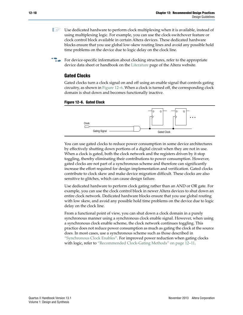
Gated ClocksGated clocks turn a clock signal on and off using an enable signal that controls gatingcircuitry, as shown in Figure 12–6. When a clock is turned off, the corresponding clockdomain is shut down and becomes functionally inactive.
You can use gated clocks to reduce power consumption in some device architecturesby effectively shutting down portions of a digital circuit when they are not in use.When a clock is gated, both the clock network and the registers driven by it stoptoggling, thereby eliminating their contributions to power consumption. However,gated clocks are not part of a synchronous scheme and therefore can significantlyincrease the effort required for design implementation and verification. Gated clockscontribute to clock skew and make device migration difficult. These clocks are alsosensitive to glitches, which can cause design failure.
Use dedicated hardware to perform clock gating rather than an AND or OR gate. Forexample, you can use the clock control block in newer Altera devices to shut down anentire clock network. Dedicated hardware blocks ensure that you use global routingwith low skew, and avoid any possible hold time problems on the device due to logicdelay on the clock line.
From a functional point of view, you can shut down a clock domain in a purelysynchronous manner using a synchronous clock enable signal. However, when usinga synchronous clock enable scheme, the clock network continues toggling. Thispractice does not reduce power consumption as much as gating the clock at the sourcedoes. In most cases, use a synchronous scheme such as those described in“Synchronous Clock Enables”. For improved power reduction when gating clockswith logic, refer to “Recommended Clock-Gating Methods” on page 12–11.
Figure 12–6. Gated Clock
Clock
Gated Clock
D Q D Q
Gating Signal
Quartus II Handbook Version 13.1 November 2013 Altera CorporationVolume 1: Design and Synthesis

Chapter 12: Recommended Design Practices 12–11Design Guidelines
Synchronous Clock EnablesTo turn off a clock domain in a synchronous manner, use a synchronous clock enablesignal. FPGAs efficiently support clock enable signals because there is a dedicatedclock enable signal available on all device registers. This scheme does not reducepower consumption as much as gating the clock at the source because the clocknetwork keeps toggling, and performs the same function as a gated clock by disablinga set of registers. Insert a multiplexer in front of the data input of every register toeither load new data, or copy the output of the register (Figure 12–7).
Recommended Clock-Gating MethodsUse gated clocks only when your target application requires power reduction andwhen gated clocks are able to provide the required reduction in your devicearchitecture. If you must use clocks gated by logic, implement these clocks using therobust clock-gating technique shown in Figure 12–8 and ensure that the gated clocksignal uses dedicated global clock routing.
You can gate a clock signal at the source of the clock network, at each register, orsomewhere in between. Because the clock network contributes to switching powerconsumption, gate the clock at the source whenever possible, so that you can shutdown the entire clock network instead of gating it further along the clock network atthe registers.
In the technique shown in Figure 12–8, a register generates the enable signal to ensurethat the signal is free of glitches and spikes. The register that generates the enablesignal is triggered on the inactive edge of the clock to be gated. Use the falling edgewhen gating a clock that is active on the rising edge, as shown in Figure 12–8. Usingthis technique, only one input of the gate that turns the clock on and off changes at atime. This prevents glitches or spikes on the output. Use an AND gate to gate a clockthat is active on the rising edge. For a clock that is active on the falling edge, use anOR gate to gate the clock and register the enable command with a positiveedge-triggered register.
Figure 12–7. Synchronous Clock Enable
Figure 12–8. Recommended Clock-Gating Technique
D Q
Enable
Data
D Q
Clock
EnableGated Clock Routed onGlobal Clock Resources
D Q D Q
Gating Signal
November 2013 Altera Corporation Quartus II Handbook Version 13.1Volume 1: Design and Synthesis

12–12 Chapter 12: Recommended Design PracticesDesign Guidelines
When using this technique, pay close attention to the duty cycle of the clock and thedelay through the logic that generates the enable signal because you must generatethe enable command in one-half the clock cycle. This situation might cause problemsif the logic that generates the enable command is particularly complex, or if the dutycycle of the clock is severely unbalanced. However, careful management of the dutycycle and logic delay may be an acceptable solution when compared with problemscreated by other methods of gating clocks.
Ensure that you apply a clock setting to the gated clock in the TimeQuest analyzer. Asshown in Figure 12–8 on page 12–11, apply a clock setting to the output of the ANDgate. Otherwise, the timing analyzer might analyze the circuit using the clock paththrough the register as the longest clock path and the path that skips the register asthe shortest clock path, resulting in artificial clock skew.
In certain cases, converting the gated clocks to clock enables may help reduce glitchand clock skew, and eventually produce a more accurate timing analysis. You can setthe Quartus II software to automatically convert gated clocks to clock enables byturning on the Auto Gated Clock Conversion option. The conversion applies to twotypes of gated clocking schemes: single-gated clock and cascaded-gated clock. TheTimeQuest analyzer supports this option for Arria® II, Arria II GX, Cyclone® II,Cyclone III, Cyclone IV, Stratix® II, Stratix II GX, Stratix III, Stratix IV, and Stratix Vdevices.
f For information about the settings and limitations of this option, refer to the “AutoGated Clock Conversion” section of the Quartus II Integrated Synthesis chapter involume 1 of the Quartus II Handbook.
Optimizing for Physical Implementation and Timing ClosureThis section provides design and timing closure techniques for high speed or complexcore logic designs with challenging timing requirements. These techniques may alsobe helpful for low or medium speed designs. Best practices for high-speed designsinclude the following:
■ Planning Physical Implementation
■ Planning FPGA Resources
■ Optimizing for Timing Closure
Planning Physical ImplementationWhen planning a design, consider the following elements of physicalimplementation:
■ The number of unique clock domains and their relationships
■ The amount of logic in each functional block
■ The location and direction of data flow between blocks
■ How data routes to the functional blocks between I/O interfaces
Quartus II Handbook Version 13.1 November 2013 Altera CorporationVolume 1: Design and Synthesis

Chapter 12: Recommended Design Practices 12–13Design Guidelines
Interface-wide control or status signals may have competing or opposing constraints.For example, when a functional block's control or status signals interface withphysical channels from both sides of the device. In such cases you must provideenough pipeline register stages to allow these signals to traverse the width of thedevice. In addition, you can structure the hierarchy of the design into separate logicmodules for each side of the device. The side modules can generate and use registeredcontrol signals per side. This simplifies floorplanning, particularly in designs withtransceivers, by placing per-side logic near the transceivers.
When adding register stages to pipeline control signals, turn off the Auto ShiftRegister Replacement option (Assignments > Settings > Analysis & SynthesisSettings > More Settings) for these registers. By default, chains of registers can beconverted to a RAM-based implementation based on performance and resourceestimates. Since pipelining helps meet timing requirements over long distance, thisassignment ensures that control signals are not converted.
Planning FPGA ResourcesThe requirements of your design affect the use of FPGA resources. Plan functionalblocks with appropriate global, regional, and dual-regional network signals in mind.In general, after allocating the clocks in a design, use global networks for the highestfan-out control signals. When a global network signal distributes a high fan-outcontrol signal, the global signal can drive logic anywhere in the device. Similarly,when using a regional network signal, the driven must be in one quadrant of thedevice, or half the device for a dual-regional network signal. Depending on data flowand physical locations of the data entry and exit between the I/Os and the device,restricting a functional block to a quadrant or half the device may not be practical forperformance or resource requirements.
When floorplanning a design, consider the balance of different types of deviceresources, such as memory, logic, and DSP blocks in the main functional blocks. Forexample, if a design is memory intensive with a small amount of logic, it may bedifficult to develop an effective floorplan. Logic that interfaces with the memorywould have to spread across the chip to access the memory. In this case, it is importantto use enough register stages in the data and control paths to allow signals to traversethe chip to access the physically disparate resources needed.
Optimizing for Timing ClosureYou can make changes to your design and constraints that help you achieve timingclosure. Whenever you change the project settings, you must balance anyperformance improvement of the setting against any potential increase in compilationtime associated with the setting. You can view the performance gain versus runtimecost by reviewing the Fitter messages after design processing.
Physical Synthesis Optimization
You can use physical synthesis optimizations for combinational logic, registerretiming, and register duplication techniques to optimize your design for timingclosure. Click Assignments > Settings > Physical Synthesis Optimizations to turnon physical synthesis options.
November 2013 Altera Corporation Quartus II Handbook Version 13.1Volume 1: Design and Synthesis

12–14 Chapter 12: Recommended Design PracticesDesign Guidelines
■ Physical synthesis for combinational logic—When the Perform physical synthesisfor combinational logic is turned on, the report panel identifies logic that physicalsynthesis can modify. You can use this information to modify the design so that theassociated optimization can be turned off to save compile time.
■ Register duplication—This technique is most useful where registers have high fan-out, or where the fan-out is in physically distant areas of the device. Review thenetlist optimizations report and consider manually duplicating registersautomatically added by physical synthesis. You can also locate the original andduplicate registers in the Chip Planner. Compare their locations, and if the fan-outis improved, modify the code and turn off register duplication to save compiletime.
■ Register retiming—This technique is particularly useful where somecombinatorial paths between registers exceed the timing goal while other pathsfall short. If a design is already heavily pipelined, register retiming is less likely toprovide significant performance gains since there should not be significantlyunbalanced levels of logic across pipeline stages.
Timing Constraint Optimization
The application of appropriate timing constraints is essential to timing closure. Usethe following general guidelines in applying timing constraints:
■ Apply multicycle constraints in your design wherever single-cycle timing analysisis not required.
■ Apply False Path constraints to all asynchronous clock domain crossings or resetsin the design. This technique prevents overconstraining and the Fitter focuses onlyon critical paths to reduce compile time. However, over constraining timingcritical clock domains can sometimes provide better timing results and lowercompile times than physical synthesis.
■ Overconstrain rather than using physical synthesis when the slack improvementfrom physical synthesis is near zero. Overconstrain the frequency requirement ontiming critical clock domains by using setup uncertainty.
■ When evaluating the effect of constraint changes on performance and runtime,compile the design with at least three different seeds to determine the averageperformance and runtime effects. Different constraint combinations producevarious results. Three samples or more establishes a performance trend. Modifyyour constraints based on performance improvement or decline.
■ Leave settings at the default value whenever possible. Increasing performanceconstraints can increase the compile time significantly. While those increases maybe necessary to close timing on a design, using the default settings wheneverpossible minimizes compile time.
Optimizing Critical Timing PathsTo close timing in high speed designs, review paths with the largest timing failures.Correcting a single, large timing failure can result in a very significant timingimprovement. Review the register placement and routing paths by clicking Tools >Chip Planner. Large timing failures on high fan-out control signals can be caused byany of the following conditions:
■ Sub-optimal use of global networks
Quartus II Handbook Version 13.1 November 2013 Altera CorporationVolume 1: Design and Synthesis

Chapter 12: Recommended Design Practices 12–15Design Guidelines
■ Signals that traverse the chip on local routing without pipelining
■ Failure to correct high fan-out by register duplication
For high-speed and high-bandwidth designs, optimize speed by reducing bus widthand wire usage. To reduce wire use, move the data as little as possible. For example, ifa block of logic functions on a few bits of a word, store inactive bits in a fifo ormemory. Memory is cheaper and denser than registers and reduces wire usage.
Power OptimizationThe total FPGA power consumption is comprised of I/O power, core static power,and core dynamic power. Knowledge of the relationship between these components isfundamental in calculating the overall total power consumption. You can use variousoptimization techniques and tools to minimize power consumption when appliedduring FPGA design implementation. The Quartus II software offers power-drivencompilation features to fully optimize device power consumption. Power-drivencompilation focuses on reducing your design’s total power consumption usingpower-driven synthesis and power-driven placement and routing.
f For more information about power-driven compilation flow and low-power designguidelines, refer to the Power Optimization chapter in volume 2 of the Quartus IIHandbook.
f For more information about power optimization techniques available for Stratix IIIdevices, refer to AN 437: Power Optimization in Stratix III FPGAs. For more informationabout power optimization techniques available for Stratix IV devices, refer to AN 514:Power Optimization in Stratix IV FPGAs. For more information about poweroptimization techniques available for Stratix V devices, refer to Reducing PowerConsumption and Increasing Bandwidth on 28-nm FPGAs white paper.
h Additionally, you can use the Quartus II PowerPlay suite of power analysis andoptimization tools to help you during the design process by delivering fast andaccurate estimations of power consumption. For more information about theQuartus II PowerPlay suite of power analysis and optimization tools, refer to AboutPower Estimation and Analysis in Quartus II Help.
MetastabilityMetastability in PLD designs can be caused by the synchronization of asynchronoussignals. You can use the Quartus II software to analyze the mean time betweenfailures (MTBF) due to metastability, thus optimizing the design to improve themetastability MTBF. A high metastability MTBF indicates a more robust design.
f For more information about how to ensure complete and accurate metastabilityanalysis, refer to the Managing Metastability With the Quartus II Software chapter involume 1 of the Quartus II Handbook.
h For more information about viewing metastability reports, refer to ViewingMetastability Reports in Quartus II Help.
November 2013 Altera Corporation Quartus II Handbook Version 13.1Volume 1: Design and Synthesis

12–16 Chapter 12: Recommended Design PracticesChecking Design Violations
Incremental CompilationThe incremental compilation feature in the Quartus II software allows you to partitionyour design hierarchy, separately compile partitions, and reuse the results forunchanged partitions. Incremental compilation flows require more up-front planningthan flat compilations, and generally require you to be more rigorous about followinggood design practices than flat compilations.
f For more information about incremental compilation and floorplan assignments, referto the Best Practices for Incremental Compilation Partitions and Floorplan Assignmentschapter in volume 1 of the Quartus II Handbook.
h For more information about incremental compilation, refer to About IncrementalCompilation in Quartus II Help.
Checking Design ViolationsTo improve the reliability, timing performance, and logic utilization of your design,you should practice good design methodology and understand how to avoid designrule violations. The Quartus II software provides the Design Assistant tool thatautomatically checks for design rule violations and reports their location.
The Design Assistant is a design rule checking tool that allows you to check for designissues early in the design flow. The Design Assistant checks your design for adherenceto Altera-recommended design guidelines. You can specify which rules you want theDesign Assistant to apply to your design. This is useful if you know that your designviolates particular rules that are not critical and you can allow these rule violations.The Design Assistant generates design violation reports with details about eachviolation based on the settings that you specified.
This section provides an introduction to the Quartus II design flow with the DesignAssistant, message severity levels, and an explanation about how to set up the DesignAssistant. The last parts of the section describe the design rules and the reportsgenerated by the Design Assistant. The Design Assistant supports all Altera devicessupported by the Quartus II software.
Quartus II Design Flow with the Design AssistantYou can run the Design Assistant after Analysis and Elaboration, Analysis andSynthesis, fitting, or a full compilation. If you set the Design Assistant to runautomatically during compilation, the Design Assistant performs a post-fitting netlistanalysis of your design. The default is to apply all of the rules to your project. If thereare some rules that are unimportant to your design, you can turn off the rules that youdo not want the Design Assistant to use.
h For more information about running the Design Assistant, refer to About the DesignAssistant in Quartus II Help.
Quartus II Handbook Version 13.1 November 2013 Altera CorporationVolume 1: Design and Synthesis
Chapter 12: Recommended Design Practices 12–17Checking Design Violations
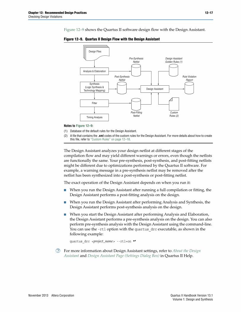
Figure 12–9 shows the Quartus II software design flow with the Design Assistant.
The Design Assistant analyzes your design netlist at different stages of thecompilation flow and may yield different warnings or errors, even though the netlistsare functionally the same. Your pre-synthesis, post-synthesis, and post-fitting netlistsmight be different due to optimizations performed by the Quartus II software. Forexample, a warning message in a pre-synthesis netlist may be removed after thenetlist has been synthesized into a post-synthesis or post-fitting netlist.
The exact operation of the Design Assistant depends on when you run it:
■ When you run the Design Assistant after running a full compilation or fitting, theDesign Assistant performs a post-fitting analysis on the design.
■ When you run the Design Assistant after performing Analysis and Synthesis, theDesign Assistant performs post-synthesis analysis on the design.
■ When you start the Design Assistant after performing Analysis and Elaboration,the Design Assistant performs a pre-synthesis analysis on the design. You can alsoperform pre-synthesis analysis with the Design Assistant using the command-line.You can use the -rtl option with the quartus_drc executable, as shown in thefollowing example:
quartus_drc <project_name> --rtl=on r
h For more information about Design Assistant settings, refer to About the DesignAssistant and Design Assistant Page (Settings Dialog Box) in Quartus II Help.
Figure 12–9. Quartus II Design Flow with the Design Assistant
Notes to Figure 12–9:(1) Database of the default rules for the Design Assistant.(2) A file that contains the .xml codes of the custom rules for the Design Assistant. For more details about how to create
this file, refer to “Custom Rules” on page 12–18.
Design Files
Analysis & Elaboration
Synthesis(Logic Synthesis &
Technology Mapping)
Fitter
Timing Analysis
Design Assistant
Pre-SynthesisNetlist
Design AssistantGolden Rules (1)
Rule ViolationReport
CustomRules (2)
Post-FittingNetlist
Post-SynthesisNetlist
November 2013 Altera Corporation Quartus II Handbook Version 13.1Volume 1: Design and Synthesis

12–18 Chapter 12: Recommended Design PracticesChecking Design Violations
Enabling and Disabling Design Assistant Rules
h For more information about enabling or disabling Design Assistant rules onindividual nodes by making an assignment in the Assignment Editor, in theQuartus II Settings File (.qsf), with the altera_attribute synthesis attribute in VerilogHDL or VHDL, or with a Tcl command, refer to Enabling Design Assistant Rules onNodes, Entities, or Instances, or Disabling Design Assistant Rules on Nodes, Entities, orInstances in Quartus II Help.
Viewing Design Assistant ResultsIf your design violates a design rule, the Design Assistant generates warningmessages and information messages about the violated rule. The Design Assistantdisplays these messages in the Messages window, in the Design Assistant Messagesreport, and in the Design Assistant report files. You can find the Design Assistantreport files called <project_name>.drc.rpt in the <project_name> subdirectory of theproject directory.
h For information about the contents of the reports generated by the Design Assistant,refer to Design Assistant Reports in Quartus II Help.
Custom RulesIn addition to the existing design rules that the Design Assistant offers, you can alsocreate your own rules and specify your own reporting format in a text file (with anyfile extension) with the XML format. You then specify the path to that file in theDesign Assistant settings page and run the Design Assistant for violation checking.
Refer to the following location to locate the file that contains the default rules for theDesign Assistant:
<Quartus II install path>\quartus\libraries\design-assistant\da_golden_rule.xml
h For more information about how to set the file path to your custom rules, refer toCustom Rules Settings Dialog Box in Quartus II Help. For more information about thebasics of writing custom rules, the Design Assistant settings, and coding examples onhow to check for clock relationship and node relationship in a design, refer to CreatingCustom Design Assistant Rules in Quartus II Help. To specify the rules that you wantthe Design Assistant to use when checking for violations, refer to Design Assistant Page(Settings Dialog Box) in Quartus II Help.
Custom Rules Coding ExamplesThe following examples of custom rules show how to check node relationships andclock relationships in a design.
Quartus II Handbook Version 13.1 November 2013 Altera CorporationVolume 1: Design and Synthesis

Chapter 12: Recommended Design Practices 12–19Checking Design Violations
Checking SR Latch Structures In a Design
Example 12–1 shows the XML codes for checking SR latch structures in a design.
In Example 12–1, the possible SR latch structures are specified in the rule definitionsection. Codes defined in the <AND></AND> block are tied together, meaning that eachstatement in the block must be true for the block to be fulfilled (AND gate similarity).In the <OR></OR> block, as long as one statement in the block is true, the block isfulfilled (OR gate similarity). If no <AND></AND> or <OR></OR> blocks are specified, thedefault is <AND></AND>.
The <FORBID></FORBID> section contains the undesirable condition for the design,which in this case is the SR latch structures. If the condition is fulfilled, the DesignAssistant highlights a rule violation.
The following examples are the undesired conditions from Example 12–1 with theirequivalent block diagrams (Figure 12–10 and Figure 12–11):
<AND><NODE_RELATIONSHIP FROM_NAME="NODE_1" FROM_TYPE="NAND" TO_NAME="NODE_2"
TO_TYPE="NAND" /><NODE_RELATIONSHIP FROM_NAME="NODE_2" FROM_TYPE="NAND" TO_NAME="NODE_1"
TO_TYPE="NAND" />
Example 12–1. Detecting SR Latches in a Design
<DA_RULE ID="EX01" SEVERITY="CRITICAL" NAME="Checking Design for SR Latch"DEFAULT_RUN="YES"><RULE_DEFINITION>
<FORBID><OR>
<NODE NAME="NODE_1" TYPE="SRLATCH" /><HAS_NODE NODE_LIST="NODE_1" /><NODE NAME="NODE_1" TOTAL_FANIN="EQ2" /><NODE NAME="NODE_2" TOTAL_FANIN="EQ2" /><AND>
<NODE_RELATIONSHIP FROM_NAME="NODE_1" FROM_TYPE="NAND" TO_NAME="NODE_2"TO_TYPE="NAND" />
<NODE_RELATIONSHIP FROM_NAME="NODE_2" FROM_TYPE="NAND" TO_NAME="NODE_1"TO_TYPE="NAND" />
</AND><AND>
<NODE_RELATIONSHIP FROM_NAME="NODE_1" FROM_TYPE="NOR" TO_NAME="NODE_2"TO_TYPE="NOR" />
<NODE_RELATIONSHIP FROM_NAME="NODE_2" FROM_TYPE="NOR" TO_NAME="NODE_1"TO_TYPE="NOR" />
</AND></OR>
</FORBID></RULE_DEFINITION>
<REPORTING_ROOT><MESSAGE NAME="Rule %ARG1%: Found %ARG2% node(s) related to this rule.">
<MESSAGE_ARGUMENT NAME="ARG1" TYPE="ATTRIBUTE" VALUE="ID" /><MESSAGE_ARGUMENT NAME="ARG2" TYPE="TOTAL_NODE" VALUE="NODE_1" />
</MESSAGE></REPORTING_ROOT></DA_RULE>
November 2013 Altera Corporation Quartus II Handbook Version 13.1Volume 1: Design and Synthesis

12–20 Chapter 12: Recommended Design PracticesChecking Design Violations
</AND>
<AND><NODE_RELATIONSHIP FROM_NAME="NODE_1" FROM_TYPE="NOR" TO_NAME="NODE_2" TO_TYPE="NOR" /><NODE_RELATIONSHIP FROM_NAME="NODE_2" FROM_TYPE="NOR" TO_NAME="NODE_1" TO_TYPE="NOR" />
</AND>
Figure 12–10. Undesired Condition 1
Figure 12–11. Undesired Condition 2
Quartus II Handbook Version 13.1 November 2013 Altera CorporationVolume 1: Design and Synthesis

Chapter 12: Recommended Design Practices 12–21Checking Design Violations
Relating Nodes to a Clock Domain
Example 12–2 shows how to use the CLOCK_RELATIONSHIP attribute to relate nodes toclock domains. This example checks for correct synchronization in data transferbetween asynchronous clock domains. Synchronization is done with cascadedregisters, also called synchronizers, at the receiving clock domain. The code inExample 12–2 checks for the synchronizer configuration based on the followingguidelines:
■ The cascading registers need to be triggered on the same clock edge
■ There is no logic between the register output of the transmitting clock domain andthe cascaded registers in the receiving asynchronous clock domain
The codes differentiate the clock domains. ASYN means asynchronous, and !ASYN meansnon-asynchronous. This notation is useful for describing nodes that are in differentclock domains. The following lines from Example 12–2 state that NODE_2 and NODE_3 arein the same clock domain, but NODE_1 is not.
<NODE_RELATIONSHIP FROM_NAME="NODE_1" TO_NAME="NODE_2" TO_PORT="D_PORT"CLOCK_RELATIONSHIP="ASYN" />
<NODE_RELATIONSHIP FROM_NAME="NODE_2" TO_NAME="NODE_3" TO_PORT="D_PORT"CLOCK_RELATIONSHIP="!ASYN" />
Example 12–2. Detecting Incorrect Synchronizer Configuration
<DA_RULE ID="EX02" SEVERITY="HIGH" NAME="Data Transfer Not Synch Correctly"DEFAULT_RUN="YES">
<RULE_DEFINITION><DECLARE>
<NODE NAME="NODE_1" TYPE="REG" /><NODE NAME="NODE_2" TYPE="REG" /><NODE NAME="NODE_3" TYPE="REG" />
</DECLARE><FORBID>
<NODE_RELATIONSHIP FROM_NAME="NODE_1" TO_NAME="NODE_2" TO_PORT="D_PORT"CLOCK_RELATIONSHIP="ASYN" />
<NODE_RELATIONSHIP FROM_NAME="NODE_2" TO_NAME="NODE_3" TO_PORT="D_PORT"CLOCK_RELATIONSHIP="!ASYN" />
<OR><NODE_RELATIONSHIP FROM_NAME="NODE_1" TO_NAME="NODE_2" TO_PORT="D_PORT"
REQUIRED_THROUGH="YES" THROUGH_TYPE="COMB" CLOCK_RELATIONSHIP="ASYN" /><CLOCK_RELATIONSHIP NAME="SEQ_EDGE|ASYN" NODE_LIST="NODE_2, NODE_3" />
</OR></FORBID></RULE_DEFINITION>
<REPORTING_ROOT><MESSAGE NAME="Rule %ARG1%: Found %ARG2% node(s) related to this rule.">
<MESSAGE_ARGUMENT NAME="ARG1" TYPE="ATTRIBUTE" VALUE="ID" /><MESSAGE_ARGUMENT NAME="ARG2" TYPE="TOTAL_NODE" VALUE="NODE_1" /><MESSAGE NAME="Source node(s): %ARG3%, Destination node(s): %ARG4%">
<MESSAGE_ARGUMENT NAME="ARG3" TYPE="NODE" VALUE="NODE_1" /><MESSAGE_ARGUMENT NAME="ARG4" TYPE="NODE" VALUE="NODE_2" />
</MESSAGE></MESSAGE></REPORTING_ROOT></DA_RULE>
November 2013 Altera Corporation Quartus II Handbook Version 13.1Volume 1: Design and Synthesis

12–22 Chapter 12: Recommended Design PracticesChecking Design Violations
The next line of code states that NODE_2 and NODE_3 have a clock relationship of eithersequential edge or asynchronous.
<CLOCK_RELATIONSHIP NAME="SEQ_EDGE|ASYN" NODE_LIST="NODE_2, NODE_3" />
The <FORBID></FORBID> section contains the undesirable condition for the design,which in this case is the undesired configuration of the synchronizer. If the conditionis fulfilled, the Design Assistant highlights a rule violation.
The following examples are the undesired conditions from Example 12–2 with theirequivalent block diagrams (Figure 12–12 and Figure 12–13):
Example 12–3.
<NODE_RELATIONSHIP FROM_NAME="NODE_1" TO_NAME="NODE_2" TO_PORT="D_PORT"CLOCK_RELATIONSHIP="ASYN" />
<NODE_RELATIONSHIP FROM_NAME="NODE_2" TO_NAME="NODE_3" TO_PORT="D_PORT"CLOCK_RELATIONSHIP="!ASYN" />
<NODE_RELATIONSHIP FROM_NAME="NODE_1" TO_NAME="NODE_2" TO_PORT="D_PORT"REQUIRED_THROUGH="YES" THROUGH_TYPE="COMB" CLOCK_RELATIONSHIP="ASYN" />
Figure 12–12. Undesired Condition 3
Example 12–4.
<NODE_RELATIONSHIP FROM_NAME="NODE_1" TO_NAME="NODE_2" TO_PORT="D_PORT"CLOCK_RELATIONSHIP="ASYN" />
<NODE_RELATIONSHIP FROM_NAME="NODE_2" TO_NAME="NODE_3" TO_PORT="D_PORT"CLOCK_RELATIONSHIP="!ASYN" />
<CLOCK_RELATIONSHIP NAME="SEQ_EDGE|ASYN" NODE_LIST="NODE_2, NODE_3" />
Figure 12–13. Undesired Condition 4
Quartus II Handbook Version 13.1 November 2013 Altera CorporationVolume 1: Design and Synthesis

Chapter 12: Recommended Design Practices 12–23Targeting Clock and Register-Control Architectural Features
Targeting Clock and Register-Control Architectural FeaturesIn addition to following general design guidelines, you must code your design withthe device architecture in mind. FPGAs provide device-wide clocks and registercontrol signals that can improve performance.
Clock Network ResourcesAltera FPGAs provide device-wide global clock routing resources and dedicatedinputs. Use the FPGA’s low-skew, high fan-out dedicated routing where available. Byassigning a clock input to one of these dedicated clock pins or with a Quartus II logicoption to assign global routing, you can take advantage of the dedicated routingavailable for clock signals.
In an ASIC design, you should balance the clock delay as it is distributed across thedevice. Because Altera FPGAs provide device-wide global clock routing resourcesand dedicated inputs, there is no need to manually balance delays on the clocknetwork.
You should limit the number of clocks in your design to the number of dedicatedglobal clock resources available in your FPGA. Clocks feeding multiple locations thatdo not use global routing may exhibit clock skew across the device that could lead totiming problems. In addition, when you use combinational logic to generate aninternal clock, it adds delays on the clock path. In some cases, delay on a clock line canresult in a clock skew greater than the data path length between two registers. If theclock skew is greater than the data delay, you violate the timing parameters of theregister (such as hold time requirements) and the design does not function correctly.
FPGAs offer a number of low-skew global routing resources to distribute high fan-outsignals to help with the implementation of large designs with many clock domains.Many large FPGA devices provide dedicated global clock networks, regional clocknetworks, and dedicated fast regional clock networks. These clocks are organized intoa hierarchical clock structure that allows many clocks in each device region with lowskew and delay. There are typically several dedicated clock pins to drive either globalor regional clock networks, and both PLL outputs and internal clocks can drivevarious clock networks.
To reduce clock skew in a given clock domain and ensure that hold times are met inthat clock domain, assign each clock signal to one of the global high fan-out, low-skewclock networks in the FPGA device. The Quartus II software automatically uses globalrouting for high fan-out control signals, PLL outputs, and signals feeding the globalclock pins on the device. You can make explicit Global Signal logic option settings byturning on the Global Signal option setting. Use this option when it is necessary toforce the software to use the global routing for particular signals.
To take full advantage of these routing resources, the sources of clock signals in adesign (input clock pins or internally-generated clocks) need to drive only the clockinput ports of registers. In older Altera device families, if a clock signal feeds the dataports of a register, the signal may not be able to use dedicated routing, which can leadto decreased performance and clock skew problems. In general, allowing clock signalsto drive the data ports of registers is not considered synchronous design and cancomplicate timing analysis.
November 2013 Altera Corporation Quartus II Handbook Version 13.1Volume 1: Design and Synthesis

12–24 Chapter 12: Recommended Design PracticesTargeting Clock and Register-Control Architectural Features
Reset ResourcesASIC designs may use local resets to avoid long routing delays. Take advantage of thedevice-wide asynchronous reset pin available on most FPGAs to eliminate theseproblems. This reset signal provides low-skew routing across the device.
The following are three types of resets used in synchronous circuits:
■ Synchronous Reset
■ Asynchronous Reset
■ Synchronized Asynchronous Reset—preferred when designing an FPGA circuit
Synchronous ResetThe synchronous reset ensures that the circuit is fully synchronous. You can easilytime the circuit with the Quartus II TimeQuest analyzer. Because clocks that aresynchronous to each other launch and latch the reset signal, the data arrival and datarequired times are easily determined for proper slack analysis. The synchronous resetis easier to use with cycle-based simulators.
There are two methods by which a reset signal can reach a register; either by beinggated in with the data input, as shown in Figure 12–14, or by using an LAB-widecontrol signal (synclr), as shown in Figure 12–15. If you use the first method, you riskadding an additional gate delay to the circuit to accommodate the reset signal, whichcauses increased data arrival times and negatively impacts setup slack. The secondmethod relies on dedicated routing in the LAB to each register, but this is slower thanan asynchronous reset to the same register.
Figure 12–14. Synchronous Reset
PRN
CLRN
D Q
DFF
inst
reset_n
data
clockout
AND2
inst1
Quartus II Handbook Version 13.1 November 2013 Altera CorporationVolume 1: Design and Synthesis

Chapter 12: Recommended Design Practices 12–25Targeting Clock and Register-Control Architectural Features
Consider two types of synchronous resets when you examine the timing analysis ofsynchronous resets—externally synchronized resets and internally synchronizedresets. Externally synchronized resets are synchronized to the clock domain outsidethe FPGA, and are not very common. A power-on asynchronous reset is dual-ranksynchronized externally to the system clock and then brought into the FPGA. Insidethe FPGA, gate this reset with the data input to the registers to implement asynchronous reset.
Figure 12–15. LAB-Wide Control Signals
Dedicated Row LAB Clocks
Local Interconnect
Local Interconnect
Local Interconnect
Local Interconnect
Local Interconnect
Local Interconnect
There are two uniqueclock signals per LAB
6
6
6
labclk0
labclkena0
labclk1 labclk2 syncload labclr1
labclkena1 labclkena2 labclr0 synclr
November 2013 Altera Corporation Quartus II Handbook Version 13.1Volume 1: Design and Synthesis

12–26 Chapter 12: Recommended Design PracticesTargeting Clock and Register-Control Architectural Features
Figure 12–16 shows the schematic for an externally synchronized reset.
Example 12–5 shows the Verilog equivalent of the schematic. When you usesynchronous resets, the reset signal is not put in the sensitivity list.
Figure 12–16. Externally Synchronized Reset
PRN
CLRN
D QPRN
CLRN
D Qpor_n
clockreset_n
data_a
INPUTVCC
VCCINPUT
VCCINPUTclock
VCCINPUTdata_b
AND2
lc 1
AND2
lc 2
PRN
CLRN
D Q
PRN
CLRN
D Q
DFF
reg1
DFF
reg2
OUTPUT out_a
out_bOUTPUT
FPGA
Example 12–5. Verilog Code for Externally Synchronized Reset
module sync_reset_ext (input clock,input reset_n,input data_a,input data_b,output out_a,output out_b);
reg reg1, reg2
assign out_a = reg1;assign out_b = reg2;
always @ (posedge clock)begin
if (!reset_n)begin
reg1 <= 1’bo;reg2 <= 1;b0;
endelsebegin
reg1 <= data_a;reg2 <= data_b;
endend
endmodule // sync_reset_ext
Quartus II Handbook Version 13.1 November 2013 Altera CorporationVolume 1: Design and Synthesis

Chapter 12: Recommended Design Practices 12–27Targeting Clock and Register-Control Architectural Features
Example 12–6 shows the constraints for the externally synchronous reset. Because theexternal reset is synchronous, you only need to constrain the reset_n signal as anormal input signal with set_input_delay constraint for -max and -min.
More often, resets coming into the device are asynchronous, and must besynchronized internally before being sent to the registers. Figure 12–17 shows aninternally synchronized reset.
Example 12–6. SDC Constraints for Externally Synchronous Reset
# Input clock - 100 MHzcreate_clock [get_ports {clock}] \
-name {clock} \-period 10.0 \-waveform {0.0 5.0}
# Input constraints on low-active reset# and dataset_input_delay 7.0 \
-max \-clock [get_clocks {clock}] \[get_ports {reset_n data_a data_b}]
set_input_delay 1.0 \-min \-clock [get_clocks {clock}] \[get_ports {reset_n data_a data_b}]
Figure 12–17. Internally Synchronized Reset
PRN
CLRN
D QPRN
CLRN
D Qreset_n
data_a
INPUTVCC
VCCINPUT
VCCINPUT
clock VCCINPUT
data_b
AND2
lc 1
AND2
lc 2
PRN
CLRN
D Q
PRN
CLRN
D Q
DFF
reg1
DFF
reg2
OUTPUT out_a
out_bOUTPUT
DFF DFF
reg3 reg4
November 2013 Altera Corporation Quartus II Handbook Version 13.1Volume 1: Design and Synthesis

12–28 Chapter 12: Recommended Design PracticesTargeting Clock and Register-Control Architectural Features
Example 12–7 shows the Verilog equivalent of the schematic. Only the clock edge is inthe sensitivity list for a synchronous reset.
Example 12–7. Verilog Code for Internally Synchronous Reset
module sync_reset (input clock,input reset_n,input data_a,input data_b,output out_a,output out_b);
reg reg1, reg2reg reg3, reg4
assign out_a = reg1;assign out_b = reg2;assign rst_n = reg4;
always @ (posedge clock)begin
if (!rst_n)begin
reg1 <= 1’bo;reg2 <= 1’b0;
endelsebegin
reg1 <= data_a;reg2 <= data_b;
endend
always @ (posedge clock)begin
reg3 <= reset_n;reg4 <= reg3;
endendmodule // sync_reset
Quartus II Handbook Version 13.1 November 2013 Altera CorporationVolume 1: Design and Synthesis

Chapter 12: Recommended Design Practices 12–29Targeting Clock and Register-Control Architectural Features
The SDC constraints are similar to the external synchronous reset, except that theinput reset cannot be constrained because it is asynchronous and should be cut with aset_false_path statement (as shown in Example 12–8) to avoid these beingconsidered as unconstrained paths.
An issue with synchronous resets is their behavior with respect to short pulses (lessthan a period) on the asynchronous input to the synchronizer flipflops. This can be adisadvantage because the asynchronous reset requires a pulse width of at least oneperiod wide to guarantee that it is captured by the first flipflop. However, this canalso be viewed as an advantage in that this circuit increases noise immunity. Spuriouspulses on the asynchronous input have a lower chance of being captured by the firstflipflop, so the pulses do not trigger a synchronous reset. In some cases, you mightwant to increase the noise immunity further and reject any asynchronous input resetthat is less than n periods wide to debounce an asynchronous input reset.
Example 12–8. SDC Constraints for Internally Synchronized Reset
# Input clock - 100 MHzcreate_clock [get_ports {clock}] \
-name {clock} \-period 10.0 \-waveform {0.0 5.0}
# Input constraints on dataset_input_delay 7.0 \
-max \-clock [get_clocks {clock}] \[get_ports {data_a data_b}]
set_input_delay 1.0 \-min \-clock [get_clocks {clock}] \[get_ports {data_a data_b}]
# Cut the asynchronous reset inputset_false_path \
-from [get_ports {reset_n}] \-to [all_registers]
November 2013 Altera Corporation Quartus II Handbook Version 13.1Volume 1: Design and Synthesis

12–30 Chapter 12: Recommended Design PracticesTargeting Clock and Register-Control Architectural Features
Figure 12–18 shows the necessary modifications that you should make to theinternally synchronized reset.
Many designs have more than one clock signal. In these cases, use a separate resetsynchronization circuit for each clock domain in the design. When you createsynchronizers for PLL output clocks, these clock domains are not reset until you lockthe PLL and the PLL output clocks are stable. If you use the reset to the PLL, this resetdoes not have to be synchronous with the input clock of the PLL. You can use anasynchronous reset for this. Using a reset to the PLL further delays the assertion of asynchronous reset to the PLL output clock domains when using internallysynchronized resets.
Asynchronous ResetAsynchronous resets are the most common form of reset in circuit designs, as well asthe easiest to implement. Typically, you can insert the asynchronous reset into thedevice, turn on the global buffer, and connect to the asynchronous reset pin of everyregister in the device. This method is only advantageous under certaincircumstances—you do not need to always reset the register. Unlike the synchronousreset, the asynchronous reset is not inserted in the data path, and does not negativelyimpact the data arrival times between registers. Reset takes effect immediately, and assoon as the registers receive the reset pulse, the registers are reset. The asynchronousreset is not dependent on the clock.
However, when the reset is deasserted and does not pass the recovery (µtSU) orremoval (µtH) time check (the TimeQuest analyzer recovery and removal analysischecks both times), the edge is said to have fallen into the metastability zone.Additional time is required to determine the correct state, and the delay can cause thesetup time to fail to register downstream, leading to system failure. To avoid this, adda few follower registers after the register with the asynchronous reset and use theoutput of these registers in the design. Use the follower registers to synchronize the
Figure 12–18. Internally Synchronized Reset with Pulse Extender
Note to Figure 12–18:(1) Junction dots indicate the number of stages. You can have more flip flops to get a wider pulse that spans more clock cycles.
PRN
CLRN
D QPRN
CLRN
D Qreset_n
data_a
INPUTVCC
VCCINPUT
VCCINPUT
clock VCCINPUT
data_b
AND2
lc 1
AND2
lc 2
PRN
CLRN
D Q
PRN
CLRN
D Q
DFF
reg1
DFF
reg2
OUTPUT out_a
out_bOUTPUT
PRN
CLRN
D QPRN
CLRN
D Q
BNAND2
Synchronizer Flip-Flops n Pulse Extender Flip-Flops
lc 3
reg3 reg4 reg5 regn
DFF DFF DFF DFF
Quartus II Handbook Version 13.1 November 2013 Altera CorporationVolume 1: Design and Synthesis

Chapter 12: Recommended Design Practices 12–31Targeting Clock and Register-Control Architectural Features
data to the clock to remove the metastability issues. You should place these registersclose to each other in the device to keep the routing delays to a minimum, whichdecreases data arrival times and increases MTBF. Ensure that these follower registersthemselves are not reset, but are initialized over a period of several clock cycles by“flushing out” their current or initial state.
Figure 12–19 shows a schematic example of this circuit.
Example 12–9 shows the equivalent Verilog code. The active edge of the reset is nowin the sensitivity list for the procedural block, which infers a clock enable on thefollower registers with the inverse of the reset signal tied to the clock enable. Thefollower registers should be in a separate procedural block as shown using non-blocking assignments.
Figure 12–19. Asynchronous Reset with Follower Registers
PRN
CLRN
D Q
DFF
reg1
PRN
CLRN
D Q
DFF
reg2
PRN
CLRN
D Q
DFF
reg3
data_a INPUTVCC
VCCINPUTreset_n
VCCINPUTclock
out_aOUTPUT
Example 12–9. Verilog Code of Asynchronous Reset with Follower Registers
module async_reset (input clock,input reset_n,input data_a,output out_a,);
reg reg1, reg2, reg3;
assign out_a = reg3;
always @ (posedge clock, negedge reset_n)begin
if (!reset_n)reg1 <= 1’b0;
elsereg1 <= data_a;
end
always @ (posedge clock)begin
reg2 <= reg1;reg3 <= reg2;
endendmodule // async_reset
November 2013 Altera Corporation Quartus II Handbook Version 13.1Volume 1: Design and Synthesis

12–32 Chapter 12: Recommended Design PracticesTargeting Clock and Register-Control Architectural Features
You can easily constrain an asynchronous reset. By definition, asynchronous resetshave a non-deterministic relationship to the clock domains of the registers they areresetting. Therefore, static timing analysis of these resets is not possible and you canuse the set_false_path command to exclude the path from timing analysis (as shownin Example 12–10). Because the relationship of the reset to the clock at the register isnot known, you cannot run recovery and removal analysis in the TimeQuest analyzerfor this path. Attempting to do so even without the false path statement results in nopaths reported for recovery and removal.
The asynchronous reset is susceptible to noise, and a noisy asynchronous reset cancause a spurious reset. You must ensure that the asynchronous reset is debounced andfiltered. You can easily enter into a reset asynchronously, but releasing a resetasynchronously can lead to potential problems (also referred to as “reset removal”)with metastability, including the hazards of unwanted situations with synchronouscircuits involving feedback.
Synchronized Asynchronous ResetTo avoid potential problems associated with purely synchronous resets and purelyasynchronous resets, you can use synchronized asynchronous resets. Synchronizedasynchronous resets combine the advantages of synchronous and asynchronousresets. These resets are asynchronously asserted and synchronously deasserted. Thistakes effect almost instantaneously, and ensures that no data path for speed isinvolved, and that the circuit is synchronous for timing analysis and is resistant tonoise.
Example 12–10. SDC Constraints for Asynchronous Reset
# Input clock - 100 MHzcreate_clock [get_ports {clock}] \
-name {clock} \-period 10.0 \-waveform {0.0 5.0}
# Input constraints on dataset_input_delay 7.0 \
-max \-clock [get_clocks {clock}]\[get_ports {data_a}]
set_input_delay 1.0 \-min \-clock [get_clocks {clock}] \[get_ports {data_a}]
# Cut the asynchronous reset inputset_false_path \
-from [get_ports {reset_n}] \-to [all_registers]
Quartus II Handbook Version 13.1 November 2013 Altera CorporationVolume 1: Design and Synthesis

Chapter 12: Recommended Design Practices 12–33Targeting Clock and Register-Control Architectural Features
Figure 12–20 shows a method for implementing the synchronized asynchronous reset.You should use synchronizer registers in a similar manner as synchronous resets.However, the asynchronous reset input is gated directly to the CLRN pin of thesynchronizer registers and immediately asserts the resulting reset. When the reset isdeasserted, logic “1” is clocked through the synchronizers to synchronously deassertthe resulting reset.
Figure 12–20. Schematic of Synchronized Asynchronous Reset
PRN
CLRN
D Q
DFF
reg3
VCC
PRN
CLRN
D Q
DFF
reg4
PRN
CLRN
D Q
DFF
reg1
PRN
CLRN
D Q
DFF
reg2
data_a
clock
INPUTVCC
VCCINPUT
VCCINPUTreset_n
VCCINPUTdata_b
out_aOUTPUT
out_bOUTPUT
November 2013 Altera Corporation Quartus II Handbook Version 13.1Volume 1: Design and Synthesis

12–34 Chapter 12: Recommended Design PracticesTargeting Clock and Register-Control Architectural Features
Example 12–11 shows the equivalent Verilog code. Use the active edge of the reset inthe sensitivity list for the blocks in Figure 12–20.
To minimize the metastability effect between the two synchronization registers, and toincrease the MTBF, the registers should be located as close as possible in the device tominimize routing delay. If possible, locate the registers in the same logic array block(LAB). The input reset signal (reset_n) must be excluded with a set_false_path
command, so the reset that comes from the synchronization register (rst_n) can betimed in the TimeQuest analyzer with recovery and removal Analysis.
Example 12–11. Verilog Code for Synchronized Asynchronous Reset
module sync_async_reset (input clock,input reset_n,input data_a,input data_b,output out_a,output out_b);
reg reg1, reg2;reg reg3, reg4;
assign out_a = reg1;assign out_b = reg2;assign rst_n = reg4;
always @ (posedge clock, negedge reset_n)begin
if (!reset_n)begin
reg3 <= 1’b0;reg4 <= 1;b0;
endelsebegin
reg3 <= 1’b1;reg4 <= reg3;
endend
always @ (posedge clock, negedge rst_n)begin
if (!rst_n)begin
reg1 <= 1’b0;reg2 <= 1;b0;
endelsebegin
reg1 <= data_a;reg2 <= data_b;
endend
endmodule // sync_async_reset
Quartus II Handbook Version 13.1 November 2013 Altera CorporationVolume 1: Design and Synthesis

Chapter 12: Recommended Design Practices 12–35Targeting Embedded RAM Architectural Features
The instantaneous assertion of synchronized asynchronous resets is susceptible tonoise and runt pulses. If possible, you should debounce the asynchronous reset andfilter the reset before it enters the device. The circuit in Figure 12–20 on page 12–33ensures that the synchronized asynchronous reset is at least one full clock period inlength. To extend this time to n clock periods, you must increase the number ofsynchronizer registers to n + 1. You must connect the asynchronous input reset(reset_n) to the CLRN pin of all the synchronizer registers to maintain the asynchronousassertion of the synchronized asynchronous reset.
f For more information about specifying the minimum routing delay, refer to the BestPractices for the Quartus II TimeQuest Timing Analyzer chapter in volume 3 of theQuartus II Handbook.
Register Control SignalsAvoid using an asynchronous load signal if the design target device architecture doesnot include registers with dedicated circuitry for asynchronous loads. Also, avoidusing both asynchronous clear and preset if the architecture provides only one ofthese control signals. Stratix III devices, for example, directly support anasynchronous clear function, but not a preset or load function. When the target devicedoes not directly support the signals, the synthesis or placement and routing softwaremust use combinational logic to implement the same functionality. In addition, if youuse signals in a priority other than the inherent priority in the device architecture,combinational logic may be required to implement the necessary control signals.Combinational logic is less efficient and can cause glitches and other problems; it isbest to avoid these implementations.
f For Verilog HDL and VHDL examples of registers with various control signals, andinformation about the inherent priority order of register control signals in Alteradevice architecture, refer to the Recommended HDL Coding Styles chapter in volume 1of the Quartus II Handbook.
Targeting Embedded RAM Architectural FeaturesAltera’s dedicated memory architecture offers many advanced features that you cantarget easily with the MegaWizard™ Plug-In Manager or with the recommended HDLcoding styles that infer the appropriate RAM megafunction (ALTSYNCRAM orALTDPRAM). Use synchronous memory blocks for your design, so that the blockscan be mapped directly into the device dedicated memory blocks. You can usesingle-port, dual-port, or three-port RAM with a single- or dual-clocking method. Youshould not infer the asynchronous memory logic as a memory block or place theasynchronous memory logic in the dedicated memory block, but implement theasynchronous memory logic in regular logic cells.
Altera memory blocks have different read-during-write behaviors, depending on thetargeted device family, memory mode, and block type. Read-during-write behaviorrefers to read and write from the same memory address in the same clock cycle; forexample, you read from the same address to which you write in the same clock cycle.
November 2013 Altera Corporation Quartus II Handbook Version 13.1Volume 1: Design and Synthesis

12–36 Chapter 12: Recommended Design PracticesConclusion
You should check how you specify the memory in your HDL code when you useread-during-write behavior. The HDL code that describes the read returns either theold data stored at the memory location, or the new data being written to the memorylocation.
In some cases, when the device architecture cannot implement the memory behaviordescribed in your HDL code, the memory block is not mapped to the dedicated RAMblocks, or the memory block is implemented using extra logic in addition to thededicated RAM block. Implement the read-during-write behavior using single-portRAM in Arria GX devices and the Cyclone and Stratix series of devices to avoid thisextra logic implementation.
f For Verilog HDL and VHDL examples and guidelines for inferring RAM functionsthat match the dedicated memory architecture in Altera devices, refer to theRecommended HDL Coding Styles chapter in volume 1 of the Quartus II Handbook.
In many synthesis tools, you can specify that the read-during-write behavior is notimportant to your design; if, for example, you never read and write from the sameaddress in the same clock cycle. For Quartus II integrated synthesis, add the synthesisattribute ramstyle=”no_rw_check” to allow the software to choose theread-during-write behavior of a RAM, rather than using the read-during-writebehavior specified in your HDL code. Using this type of attribute prevents thesynthesis tool from using extra logic to implement the memory block and, in somecases, can allow memory inference when it would otherwise be impossible.
f For details about using the ramstyle attribute, refer to the Quartus II IntegratedSynthesis chapter in volume 1 of the Quartus II Handbook. For information about thesynthesis attributes in other synthesis tools, refer to your synthesis tooldocumentation, or to the appropriate chapter in the Synthesis section in volume 1 ofthe Quartus II Handbook.
ConclusionFollowing the design practices described in this chapter can help you to consistentlymeet your design goals. Asynchronous design techniques may result in incompletetiming analysis, may cause glitches on data signals, and may rely on propagationdelays in a device leading to race conditions and unpredictable results. Takingadvantage of the architectural features in your FPGA device can also improve thequality of your results.
Document Revision HistoryTable 12–1 shows the revision history for this chapter.
Table 12–1. Document Revision History (Part 1 of 2)
Date Version Changes
November 2013 13.1.0 Removed HardCopy device information.
May 2013 13.0.0■ Added “Optimizing for Physical Implementation and Timing Closure” section.
■ Removed PrimeTime support.
June 2012 12.0.0 Removed survey link.
Quartus II Handbook Version 13.1 November 2013 Altera CorporationVolume 1: Design and Synthesis

Chapter 12: Recommended Design Practices 12–37Document Revision History
f For previous versions of the Quartus II Handbook, refer to the Quartus II HandbookArchive.
November 2011 11.0.1 Template update.
May 2011 11.0.0 Added information to “Reset Resources” on page 12–24.
December 2010 10.1.0
■ Title changed from Design Recommendations for Altera Devices and the Quartus IIDesign Assistant.
■ Updated to new template.
■ Added references to Quartus II Help for “Metastability” on page 9–13 and“Incremental Compilation” on page 9–13.
■ Removed duplicated content and added references to Quartus II Help for “CustomRules” on page 9–15.
July 2010 10.0.0
■ Removed duplicated content and added references to Quartus II Help for DesignAssistant settings, Design Assistant rules, Enabling and Disabling Design AssistantRules, and Viewing Design Assistant reports.
■ Removed information from “Combinational Logic Structures” on page 5–4
■ Changed heading from “Design Techniques to Save Power” to “PowerOptimization” on page 5–12
■ Added new “Metastability” section
■ Added new “Incremental Compilation” section
■ Added information to “Reset Resources” on page 5–23
■ Removed “Referenced Documents” section
November 2009 9.1.0 ■ Removed documentation of obsolete rules.
March 2009 9.0.0 ■ No change to content.
November 2008 8.1.0
■ Changed to 8-1/2 x 11 page size
■ Added new section “Custom Rules Coding Examples” on page 5–18
■ Added paragraph to “Recommended Clock-Gating Methods” on page 5–11
■ Added new section: “Design Techniques to Save Power” on page 5–12
May 2008 8.0.0
■ Updated Figure 5–9 on page 5–13; added custom rules file to the flow
■ Added notes to Figure 5–9 on page 5–13
■ Added new section: “Custom Rules Report” on page 5–34
■ Added new section: “Custom Rules” on page 5–34
■ Added new section: “Targeting Embedded RAM Architectural Features” onpage 5–38
■ Minor editorial updates throughout the chapter
■ Added hyperlinks to referenced documents throughout the chapter
Table 12–1. Document Revision History (Part 2 of 2)
Date Version Changes
November 2013 Altera Corporation Quartus II Handbook Version 13.1Volume 1: Design and Synthesis

12–38 Chapter 12: Recommended Design PracticesDocument Revision History
Quartus II Handbook Version 13.1 November 2013 Altera CorporationVolume 1: Design and Synthesis