10Gb/s CWDM SFP+ Optical Transceiver TR-LXxxL-N00 · This SFP+ CWDM transceiver is designed to...
14
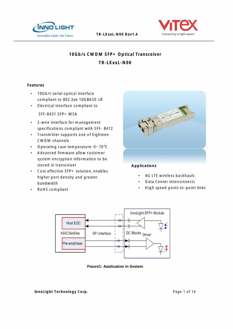
InnoLight Technology Corp. Page 1 of 14 TR-LXxxL-N00 Rev1.4 Features • 10Gb/s serial optical interface compliant to 802.3ae 10GBASE-LR • Electrical interface compliant to SFF-8431 SFP+ MSA • 2-wire interface for management specifications compliant with SFF- 8472 • Transmitter supports one of Eighteen CWDM channels • Operating case temperature: 0~70°C • Advanced firmware allow customer system encryption information to be stored in transceiver • Cost effective SFP+ solution, enables higher port density and greater bandwidth • RoHS compliant Applications • 4G LTE wireless backhauls • Data Center interconnects • High speed point-to-point links 10Gb/s CWDM SFP+ Optical Transceiver TR-LXxxL-N00 Figure1: Application in System
Transcript of 10Gb/s CWDM SFP+ Optical Transceiver TR-LXxxL-N00 · This SFP+ CWDM transceiver is designed to...
InnoLight Technology Corp. Page 1 of 14
TR-LXxxL-N00 Rev1.4
Features
• 10Gb/s serial optical interfacecompliant to 802.3ae 10GBASE-LR
• Electrical interface compliant to
SFF-8431 SFP+ MSA
• 2-wire interface for managementspecifications compliant with SFF- 8472
• Transmitter supports one of EighteenCWDM channels
• Operating case temperature: 0~70°C• Advanced firmware allow customer
system encryption information to bestored in transceiver
• Cost effective SFP+ solution, enableshigher port density and greaterbandwidth
• RoHS compliant
Applications
• 4G LTE wireless backhauls• Data Center interconnects• High speed point-to-point links
10Gb/s CWDM SFP+ Optical Transceiver
TR-LXxxL-N00
Figure1: Application in System
InnoLight Technology Corp. Page 2 of 14
TR-LXxxL-N00 Rev1.4
1. GENERAL DESCRIPTION
This SFP+ CWDM transceiver is designed to transmit and receive optical data over single mode optical fiber for link length 10km. (for longer wavelength, maybe need EML TOSA solution)
The SFP+ CWDM module electrical interface is compliant to SFI electrical specifications. The transmitter input and receiver output impedance is 100 Ohms differential. Data lines are internally AC coupled. The module provides differential termination and reduce differential to common mode conversion for quality signal termination and low EMI. SFI typically operates over 200 mm of improved FR4 material or up to about 150mm of standard FR4 with one connector.
The transmitter converts up to 10 Gb/s serial PECL or CML electrical data into serial optical data compliant with the 10GBASE-LR standard. An open collector compatible Transmit Disable (Tx_Dis) is provided. Logic “1” or no connection on this pin will disable the laser from transmitting. Logic “0” on this pin provides normal operation. The transmitter has an internal automatic power control loop (APC) to ensure constant optical power output across supply voltage and temperature variations. An open collector compatible Transmit Fault (Tx_Fault) is provided. TX_Fault is module output contact that when high, indicates that the module transmitter has detected a fault condition related to laser operation or safety. The TX_Fault output contact is an open drain/collector and shall be pulled up to the Vcc_Host in the host with a resistor in the range 4.7-10 kΩ. TX_Disable is a module input contact. When TX_Disable is asserted high or left open, the SFP+ module transmitter output shall be turned off. This contact shall be pulled up to VccT with a 4.7 kΩ to 10 kΩ resistor
The receiver converts up to 10G/s serial optical data into serial PECL/CML electrical data. An open collector compatible Loss of Signal is provided. Rx_LOS when high indicates an optical signal level below that specified in the relevant standard. The Rx_LOS contact is an open drain/collector output and shall be pulled up to Vcc_Host in the host with a resistor in the range 4.7-10 kΩ, or with an active termination. Power supply filtering is recommended for both the transmitter and receiver. The Rx_LOS signal is intended as a preliminary indication to the system in which the SFP+ is installed that the received signal strength is below the specified range. Such an indication typically points to non-installed cables, broken cables, or a disabled, failing or a powered off transmitter at the far end of the cable.

InnoLight Technology Corp. Page 3 of 14
TR-LXxxL-N00 Rev1.4
2. PROPOSED APPLICATION SCHEMATICS
InnoLight Technology Corp. Page 4 of 14
TR-LXxxL-N00 Rev1.4
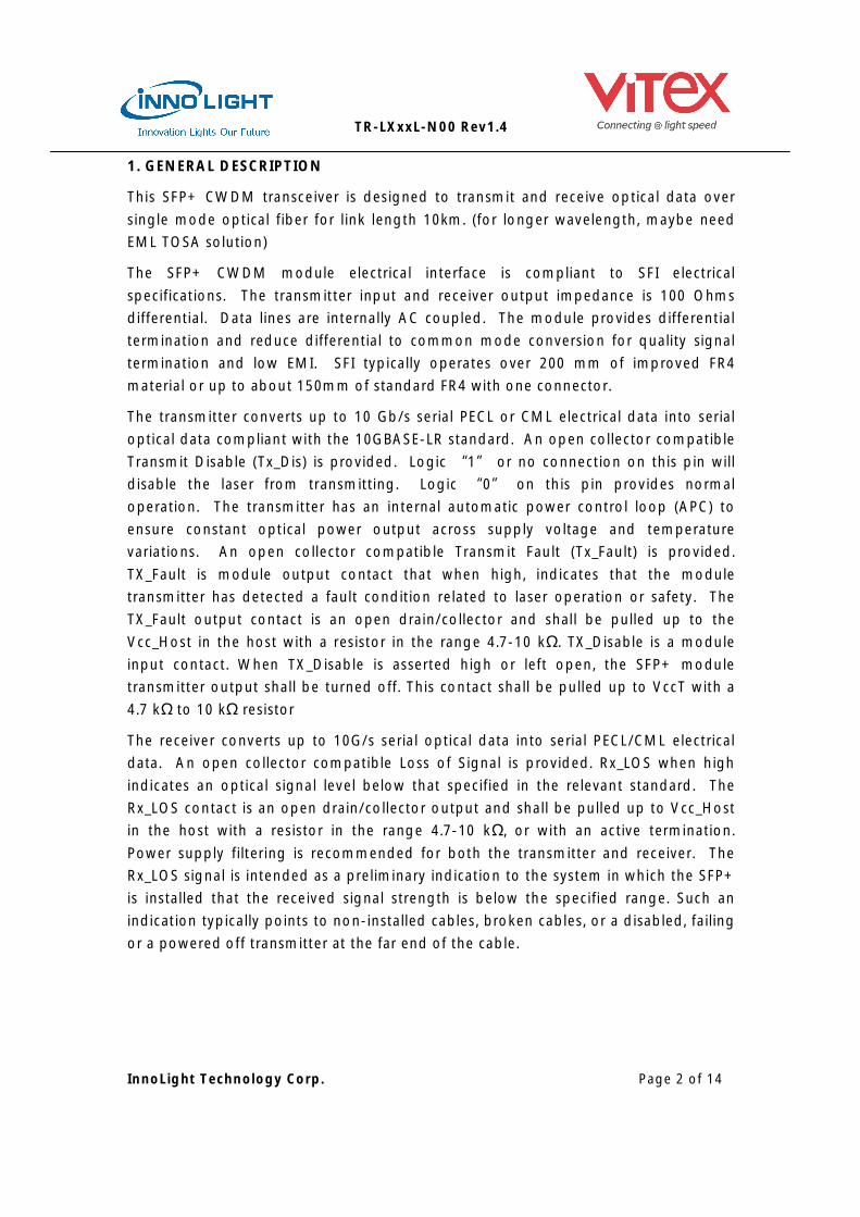
3. PIN DEFINITION
The SFP+ modules are hot-pluggable. Hot pluggable refers to plugging in or unplugging a module while the host board is powered. The SFP+ host connector is a 0.8 mm pitch 20 position right angle improved connector specified by SFF-8083, or stacked connector with equivalent with equivalent electrical performance. Host PCB contact assignment is shown in Figure 2 and contact definitions are given in the Pin Description table. SFP+ module contacts mates with the host in the order of ground, power, followed by signal as illustrated by Figure 3 and the contact sequence order listed in the Pin Description table.
Figure 3: Module Contact Assignment
Figure 2: Module Interface to Host

InnoLight Technology Corp. Page 5 of 14
TR-LXxxL-N00 Rev1.4
Pin Description
PIN Logic Symbol Name / Description Note
1 VeeT Module Transmitter Ground 1
2 LVTTL-O TX_Fault Module Transmitter Fault
3 LVTTL-I TX_Dis
Transmitter Disable; Turns off transmitter laser
output
4 LVTTL-I/O SDA 2-Wire Serial Interface Data Line 2
5 LVTTL-I SCL 2-Wire Serial Interface Clock 2
6 MOD_ABS Module Definition, Grounded in the module
7 LVTTL-I RS0 Receiver Rate Select
8 LVTTL-O RX_LOS Receiver Loss of Signal Indication Active LOW 2
9 LVTTL-I RS1 Transmitter Rate Select
10 VeeR Module Receiver Ground 1
11 VeeR Module Receiver Ground 1
12 CML-O RD- Receiver Inverted Data Output
13 CML-O RD+ Receiver Data Output
14 VeeR Module Receiver Ground 1
15 VccR Module Receiver 3.3 V Supply
16 VccT Module Receiver 3.3 V Supply
17 VeeT Module Transmitter Ground 1
18 CML-I TD+ Transmitter Non-Inverted Data Input
19 CML-I TD- Transmitter Inverted Data Input
20 VeeT Module Transmitter Ground 1
Note:
1. Module ground pins GND are isolated from the module case.
2. Shall be pulled up with 4.7K-10Kohms to a voltage between 3.15V and 3.45V on the
host board.
InnoLight Technology Corp. Page 6 of 14
TR-LXxxL-N00 Rev1.4
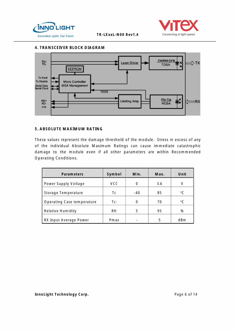
4. TRANSCEIVER BLOCK DIAGRAM
5. ABSOLUTE MAXIMUM RATING
These values represent the damage threshold of the module. Stress in excess of any of the individual Absolute Maximum Ratings can cause immediate catastrophic damage to the module even if all other parameters are within Recommended Operating Conditions.
Parameters Symbol Min. Max. Unit
Power Supply Voltage VCC 0 3.6 V
Storage Temperature Tc -40 85 °C
Operating Case temperature Tc: 0 70 °C
Relative Humidity RH 5 95 %
RX Input Average Power Pmax - 5 dBm
InnoLight Technology Corp. Page 7 of 14
TR-LXxxL-N00 Rev1.4
6. RECOMMENDED OPERATING ENVIRONMENT
Recommended Operating Environment specifies parameters for which the electrical and optical characteristics hold unless otherwise noted.
Parameters Symbol Min. Typical Max Unit
Power Supply Voltage VCC 3.135 3.3 3.465 V
Power Supply Current Icc 420 mA
Operating Case Temperature Tc 0 70 °C
7. OPTICAL CHARACTERISTICS
The following optical characteristics are defined over the Recommended Operating
Environment unless otherwise specified.
Parameter Symbol Min. Typical Max Unit Note
Operating Reach 10 km
Transmitter
Center wavelength λ Ref order
information nm
Side Mode
Suppression Ratio SMSR 30 dB
Optical spectrum
width(-20dB) 1 nm
Launched power Po -1 3 dBm
Center Wavelength
Stability ΔλD -6.5 6.5 nm
Launched power in
OMA -3.2 dBm
Transmitter and
dispersion penalty DP 2 dB 4
Average launch power
of OFF transmitter Poff -30 dBm
Extinction ratio ER 3.5 dB
InnoLight Technology Corp. Page 8 of 14
TR-LXxxL-N00 Rev1.4
RIN RIN -128 dB/Hz
Optical Return Loss
Tolerance RL 12 dB
Receiver
Center wavelength λ 1260 - 1620 nm
Receiver Overload 0.5 dB
Receiver Sensitivity RSEN -15 dBm 1
Receiver sensitivity
in OMA -14.6 dBm 2
Receiver
Reflectance Rf -12 dB
Stressed receiver
sensitivity in OMA -12 dBm
Vertical eye closure
penalty 2.2 dB 3
LOS Assert LOSA -28 dBm
LOS De-assert LOSD -16 dBm
LOS Hysteresis 0.5 dB
Stressed eye jitter 0.3 UI 2
Receive electrical
3dB upper cutoff
frequency
12.5 GHz
Receiver power
(damage) 5 dBm
Notes:
1. Average optical power shall be measured using the methods specified in TIA/EIA-
455-95.
2. Receiver sensitivity is informative. Stressed receiver sensitivity shall be measured
with conformance test signal for BER =1x 10-12.
InnoLight Technology Corp. Page 9 of 14
TR-LXxxL-N00 Rev1.4
3. Vertical eye closure penalty and stressed eye jitter are the test conditions for
measuring stressed receiver sensitivity. They are not the required characteristic of
the receiver.
4. Path penalty is intended as the power penalty of the interface between back-to-
back and the maximum applied dispersion.
8. DIGITAL DIAGNOSTIC FUNCTIONS
The following digital diagnostic characteristics are defined over the Recommended Operating Environment unless otherwise specified. It is compliant to SFF-8472 Rev10.2 with internal calibration mode. For external calibration mode please contact our sales staff.
Parameter Symbol Min. Max Unit Note
Temperature monitor
absolute error DMI_Temp -3 3 degC
Over
operating
temp
Laser power monitor
absolute error DMI_TX -3 3 dB
RX power monitor
absolute error DMI_RX -3 3 dB
-1dBm to
-15dBm
range
Supply voltage
monitor absolute
error
DMI_VCC -0.08 0.08 V
Full
operating
range
Bias current monitor DMI_Ibias -10% 10% mA

InnoLight Technology Corp. Page 10 of 14
TR-LXxxL-N00 Rev1.4
9. ELECTRICAL CHARACTERISTICS
The following electrical characteristics are defined over the Recommended Operating Environment unless otherwise specified.
Parameter Symbol Min. Typical Max Unit Note
Data Rate 10.3125 Gb/s
Power consumption - 900 1450 mW
Transmitter
Single Ended Output
Voltage Tolerance -0.3 - 4 V
AC common mode voltage
tolerance 15 - - mV
Tx Input Diff Voltage VI 180 700 mV
Tx Fault Low Vol -0.3 0.4 V
Tx Fault High Voh 2 VCC V
Data Dependent Input Jitter DDJ 0.1 UI
Data Input Total Jitter TJ 0.28 UI
Receiver
Single Ended Output
Voltage Tolerance -0.3 - 4 V
Rx Output Diff Voltage Vo 300 850 mV
Rx Output Rise and Fall
Time Tr/Tf 30 ps
20% to
80%
Total Jitter TJ 0.7 UI
Deterministic Jitter DJ 0.42 UI
InnoLight Technology Corp. Page 11 of 14
TR-LXxxL-N00 Rev1.4
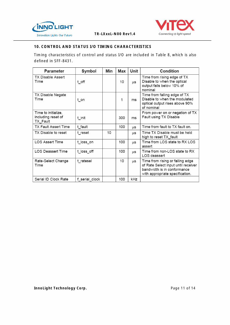
10. CONTROL AND STATUS I/O TIMING CHARACTERISTICS
Timing characteristics of control and status I/O are included in Table 8, which is also defined in SFF-8431.
InnoLight Technology Corp. Page 12 of 14
TR-LXxxL-N00 Rev1.4
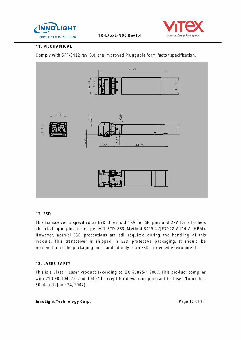
11. MECHANICAL
Comply with SFF-8432 rev. 5.0, the improved Pluggable form factor specification.
12. ESD
This transceiver is specified as ESD threshold 1KV for SFI pins and 2kV for all others electrical input pins, tested per MIL-STD-883, Method 3015.4 /JESD22-A114-A (HBM). However, normal ESD precautions are still required during the handling of this module. This transceiver is shipped in ESD protective packaging. It should be removed from the packaging and handled only in an ESD protected environment.
13. LASER SAFTY
This is a Class 1 Laser Product according to IEC 60825-1:2007. This product complies with 21 CFR 1040.10 and 1040.11 except for deviations pursuant to Laser Notice No. 50, dated (June 24, 2007)
InnoLight Technology Corp. Page 13 of 14
TR-LXxxL-N00 Rev1.4
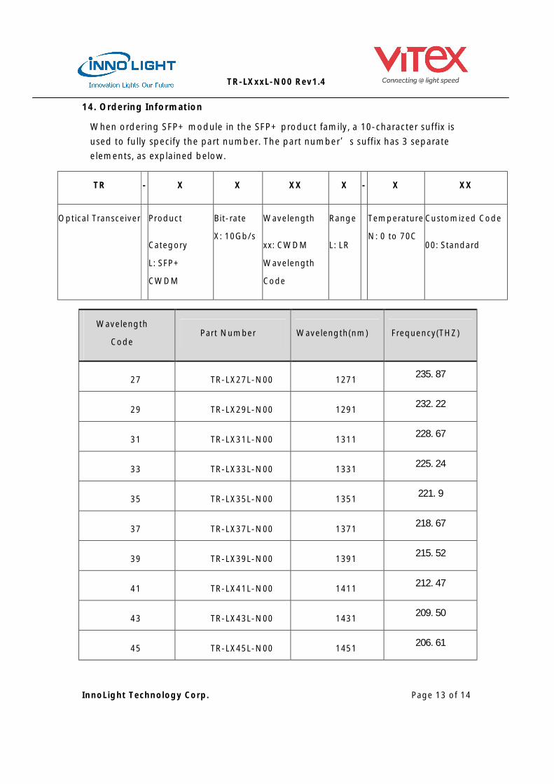
14. Ordering Information
When ordering SFP+ module in the SFP+ product family, a 10-character suffix is used to fully specify the part number. The part number’s suffix has 3 separate elements, as explained below.
TR - X X XX X - X XX
Optical Transceiver Product
Category
L: SFP+
CWDM
Bit-rate
X: 10Gb/s
Wavelength
xx: CWDM
Wavelength
Code
Range
L: LR
Temperature
N: 0 to 70C
Customized Code
00: Standard
Wavelength
Code Part Number Wavelength(nm) Frequency(THZ)
27 TR-LX27L-N00 1271 235.87
29 TR-LX29L-N00 1291 232.22
31 TR-LX31L-N00 1311 228.67
33 TR-LX33L-N00 1331 225.24
35 TR-LX35L-N00 1351 221.9
37 TR-LX37L-N00 1371 218.67
39 TR-LX39L-N00 1391 215.52
41 TR-LX41L-N00 1411 212.47
43 TR-LX43L-N00 1431 209.50
45 TR-LX45L-N00 1451 206.61
InnoLight Technology Corp. Page 14 of 14
TR-LXxxL-N00 Rev1.4
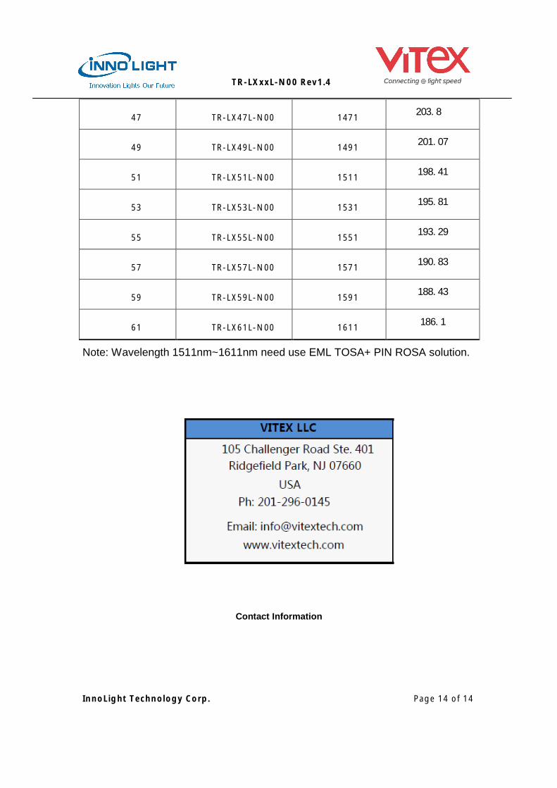
Note: Wavelength 1511nm~1611nm need use EML TOSA+ PIN ROSA solution.
47 TR-LX47L-N00 1471 203.8
49 TR-LX49L-N00 1491 201.07
51 TR-LX51L-N00 1511 198.41
53 TR-LX53L-N00 1531 195.81
55 TR-LX55L-N00 1551 193.29
57 TR-LX57L-N00 1571 190.83
59 TR-LX59L-N00 1591 188.43
61 TR-LX61L-N00 1611 186.1
Contact Information