
1063_101D_issG_PUBLISHED_WEB
16
DSP Noise Cancellation module For Icom F series commercial radios and repeaters Installation Information bhi 1063-101D Issue F IC-F2010/F2020 IC-F30/F31GT/GS IC-F40/F41GT/GS IC-F510/F520 IC-F610/F620 IC-FR310/F4100 repeaters IC-F15 IC-F25 IC-F34GT/GS IC-F44GT/GS Models covered: IC-F300/F400/S IC-F3/F4/S IC-F3GT/GS IC-F4GT/GS IC-F1010/F1020 IC-F14 IC-F24 IC-F33GT/GS IC-43GT/GS NNTDSP.001 Sound Engineering Solutions bhi If you have any queries regarding the range of bhi products then please visit our website or contact us on the number above. DSP Noise Cancellation bhi Ltd PO Box 318 Burgess Hill West Sussex RH15 9NR Tel: + 44 (0)845 217 9926 Fax: +44 (0) 845 217 9936 email:[email protected] www.bhi-ltd.co.uk
-
Upload
pw-publishing-limited -
Category
Documents
-
view
216 -
download
3
description
NNTDSP.001 Installation Information NNTDSP.001 Fitting instructions NNTDSP.001 Fitting instructions Page 1 Models covered: IC-F300/F400/S IC-F3/F4/S IC-F3GT/GS IC-F4GT/GS IC-F1010/F1020 IC-F14 IC-F24 IC-F33GT/GS IC-43GT/GS Tel: + 44 (0)845 217 9926 Fax: +44 (0) 845 217 9936 IC-F2010/F2020 IC-F30/F31GT/GS IC-F40/F41GT/GS IC-F510/F520 IC-F610/F620 IC-FR310/F4100 repeaters IC-F15 IC-F25 IC-F34GT/GS IC-F44GT/GS email:[email protected] www.bhi-ltd.co.uk 1063-101D Issue F Page 32
Transcript of 1063_101D_issG_PUBLISHED_WEB

NNTDSP.001 Fitting instructionsNNTDSP.001 Fitting instructions Page 1
DSP Noise Cancellation moduleFor Icom F series commercial radios
and repeaters
Installation Information
bhi
1063-101DIssue F
IC-F2010/F2020IC-F30/F31GT/GSIC-F40/F41GT/GS
IC-F510/F520IC-F610/F620
IC-FR310/F4100 repeatersIC-F15 IC-F25
IC-F34GT/GS IC-F44GT/GS
Models covered:IC-F300/F400/SIC-F3/F4/SIC-F3GT/GSIC-F4GT/GSIC-F1010/F1020IC-F14 IC-F24IC-F33GT/GS IC-43GT/GS
NNTDSP.001
Page 32
So
und E
ngine
ering
Solu
tions
bhi
If you have any queries regarding the range of bhi products then please visit our website or contact us on the number above.
DSP Noise Cancellation
bhi LtdPO Box 318Burgess Hill
West SussexRH15 9NR
Tel: + 44 (0)845 217 9926Fax: +44 (0) 845 217 9936
email:[email protected]

NNTDSP.001 Fitting instructionsNNTDSP.001 Fitting instructionsPage 2
Copyright
This publication, including all photographs and illustrations is protected under international copyright laws, with all rights reserved. Neither this manual, nor any of the material within, may be copied or reproduced without the written consent of bhi Ltd.
Disclaimer
The information in this document is subject to change without notice. bhi Ltd. makes no representations or warranties with respect to the contents hereof and specifically disclaims any implied warranties of merchantability or fitness for any particular purpose. Furthermore, bhi Ltd. reserves the right to revise this publication and to make changes from time to time in the content hereof without obligation of bhi Ltd. to notify any person of such revision or changes.The fitting of the bhi NNTDSP.001 module may involve the removal of small surface mount components and cutting pads. This should only be carried out by a qualified engineer. bhi accepts no responsibility for the fitting or installation of the NNTDSP.001 module and are not liable for any damage to equipment caused by its fitment. Fitting this module may invalidate your warranty.
All attempts have been made to ensure that this information is up to date. It is possible that these instructions contain errors, or the equipment is slightly different to the one used to compile this information. In all cases it is up to the installer to ensure that the module is fitted correctly.
Please read these instructions thoroughly before attempting to fit the NNTDSP.001 module.
By installing this module you are doing so at your own risk.
Important Information
Page 31
PCB versionNEDSP1062-PCB.Basic amplified DSP module. Noise cancellation levels selectable from jumpers on the module. DSP functions are avaialble on the PCB pins to allow remote operation of the module.Supplied with full fitting instructions.
Keyboard versionNEDSP1062-KBD.KBD version incorporates a dual button keyboard to control all functions of the module. Audio bypasses the module when power is removed, or switched off. The module is supplied complete with all mounting hardware, prewired power connector, labels and full fitting intructions. 4 or 8 noise cancellation levels can be selected.
4.7 NEDSP1062AmplifiedDSPmodule.Amplifed DSP modulefor installation beforethe loudspeaker oraudio output device.These modules are ideally suited for integration into the receiving side of communication equipment.
Specification:Noise cancellation levels 8Noise cancellation 9 - 35dBTone reduction 4 - 65dBAudio bandwidth 50 -4.3KHzMax power 3 W(4R)Power supply 12 - 18VCurrent consumption 500mASize 37 x 50mm
Specification:Noise cancellation levels 4/8Noise cancellation 9 - 35dBTone reduction 4 - 65dBAudio bandwidth 50 -4.3KHzMax power 3 W(4R)Power supply 12 - 18VCurrent consumption 500mASize 37 x 50mm
Power ampPre amp NEDSP1062
Audio source Speaker

NNTDSP.001 Fitting instructionsNNTDSP.001 Fitting instructions Page 3
Contents
1. Introduction.........................................................4
2. Module overview.................................................6 2.1 Icom modification 6 2.2 Change the board default settings 7 2.3 Functions of the different pads 7 2.4 How to modify the pads 7 2.5 Control pad locations 8 2.6 Important fitting instructions 8 2.7 Specifications 8 2.8 Connector pin-out 9 2.9 Physical dimensions 9
3. Icomfittinginstructions....................................10 3.1 IC-F300/F400/S 10 3.2 IC-F3/F4/S 12 3.3 IC-F3GT/GS, IC-F4GT/GS 18 3.4 IC-F1010/F1020/F2010/F2020 20 3.5 IC-F30/F31GT/GS, IC-F40/F41/GT/GS 21 3.6 IC-F510/F520, IC-F610/F620 23 3.7 IC-FR3100/FR4100 24 3.8 IC-14/IC-F15 IC-F24/IC-F25 26 3.9 IC-F33/F34 F43/F44GT/GS 27
4. Other bhi products..................................................28
4.1 NES10-2 MKII Noise eliminating speaker 28 4.2 NES5 Noise eliminating speaker 28 4.3 NEIM1031 Noise eliminating inline module 29 4.4 NEIM1031 accessories 29 4.5 1042 Switch box 29 4.6 NEDSP1061 Low level signal DSP module 30 4.7 NEDSP1062 Amplified DSP module 31
Page 30
Oth
er b
hi p
rod
uct
s
4.6 NEDSP1061 Low level DSP module.Low level signal DSP processor. Inserts in to the audio path of problemsignals to provide effective noise and interefence removal. This can be in the microphone path or receive path. The modulesare suited for retrofitting or designing into new equipment. Input and output level controls allow the units to be easily incorporated into most equipment.
PCB versionNEDSP1061-PCB.Basic DSP module. Noise cancellation levels selectable from jumpers on the module. DSP functions are available on the PCB pins to allow remote operation of the module.Supplied with full fitting instructions.
Keyboard versionNEDSP1061-KBD.KBD version incorporates a single button keyboard to control all the functions of the module. 4 DSP levels available. Supplied with mounting hardware, labels and full fitting instructions.
Specification:Noise cancellation levels 8Noise cancellation 9 - 35dBTone reduction 4 - 65dBAudio bandwidth 50 - 4.3KHz Power supply 5 - 15VCurrent consumption 45mASize 27 x 36mm
Specification:Noise cancellation levels 4Noise cancellation 11 - 35dBTone reduction 5 - 65dB Audio bandwidth 50 - 4.3KHzPower supply 5 - 15VCurrent consumption 45mASize 27 x 36mm
NEDSP1061Pre amp Power amp
Audio source Audio out
NNTDSP.001 Fitting instructionsNNTDSP.001 Fitting instructionsPage 4
1. Introduction.The unique NNTDSP.001 noise eliminating DSP board will allow clear verbal radio communication from a user where there is high ambient noise, without the use of a full fleet of headsets, complicated programming or soldering.
The NNTDSP.001 DSP board is ideal for a variety of environments including construction sites, motorsport, airports, noisy factories and dockyards, in fact any-where there is high background noise. For example, on construction sites, loud noises are generated from various pieces of machinery such as site generators and pneumatic drills. The worker in this environment, using an Icom radio, transmits audio which has all the construction noises superimposed on it. On each of the receiving radios that have the DSP module fitted, the unwanted noise is removed and the user can hear clearly what is being said. Motor sport is another fantastic application for this product. At any track there are high levels of noise generated and no matter how you put a microphone into the headset of a driver, the noise gets transmitted and there’s no way of stopping Wind noise, gearbox noise, engine noise, and tyre noise that get transmitted with the same signal. With the Icom radio, just press the assigned noise-cancelling button and the noise is removed.
The NNTDSP.001 DSP board operates on most Icom ‘F’ series commercial radios and repeaters that have an internal accessory socket. This new device uses an innovative process of noise reduction that operates in the frequency domain. The pass-band of the digital signal processing (DSP) technology is subdivided into sub-bands. The system then works out whether the signal has speech or noise characteristics in the sub-band. If the signal has noise characteristics, the noise portion is removed from this sub-band, depending on the filter level used. If no noise is present the speech remains unchanged. The system is fully adaptive and adjusts itself continuously to changing environmental conditions. When the signal is first received the DSP automatically adjusts to the characteristics of the voice signal and noise within 1 second and then continuously removes the unwanted noise for the rest of the transmission.
The module is installed in the “Option” socket and a small modification is required in the radio to enable the module to work. This modification cuts the audio path of the loudspeaker and allows the insertion of the DSP board. The programming software is set up to
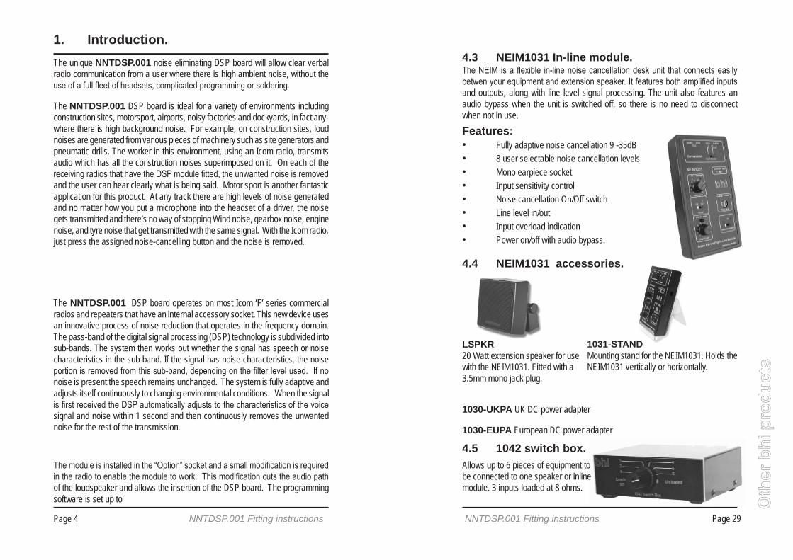
Page 29
4.3 NEIM1031 In-line module.The NEIM is a flexible in-line noise cancellation desk unit that connects easily betwen your equipment and extension speaker. It features both amplified inputs and outputs, along with line level signal processing. The unit also features an audio bypass when the unit is switched off, so there is no need to disconnect when not in use.Features:• Fully adaptive noise cancellation 9 -35dB• 8 user selectable noise cancellation levels• Mono earpiece socket• Input sensitivity control• Noise cancellation On/Off switch• Line level in/out• Input overload indication• Power on/off with audio bypass.
4.4 NEIM1031 accessories.
LSPKR20 Watt extension speaker for use with the NEIM1031. Fitted with a 3.5mm mono jack plug.
1031-STANDMounting stand for the NEIM1031. Holds the NEIM1031 vertically or horizontally.
Oth
er b
hi p
rod
uct
s
4.5 1042 switch box.Allows up to 6 pieces of equipment to be connected to one speaker or inline module. 3 inputs loaded at 8 ohms.
1030-UKPA UK DC power adapter
1030-EUPA European DC power adapter

NNTDSP.001 Fitting instructionsNNTDSP.001 Fitting instructions Page 5
“enable OPT 1” on one of the assignable buttons such as P0 to P3 on the mobiles or if used with a handportable there are also the buttons above and below the PTT. Noise level is set at 6; this is adjustable by links on the module.
Figure 1. Noise cancellation.
Original signal.Speech with a lot of background noise
Processed speech.Speech with reduced noise
Speech Noise
Reduced noise
The following diagrams are taken from actual audio signals and illustrate how the signal is being processed.
Page 28
4. Other bhi productsOther noise cancellation products from bhi. Visit www.bhi-ltd.co.uk for more information.
DSP noise cancellation built into a compact speaker unit. the unit provides an easy to install solution to noise reduction
Features:• Fully adaptive noise cancellation 9 -35dB• 8 user selectable noise cancellation levels• Mono earpiece socket• Input sensitivity control• Noise cancellation On/Off switch• Power on/off/audio bypass• LED indication of power and noise cancellation• 12-24VDC operation• Compact robust speaker unit.• Greatly improved signal to noise ratio• Easy to install with adjustable mounting bracket• Optional extras available.
4.1 NES10-2MKII Noise Eliminating speaker.
Basic plug and go noise cancelling speaker preset to 20dB of noise reduction.
Features:• Fully adaptive noise cancellation 20dB• 12-24VDC operation• Compact robust speaker unit.• Greatly improved signal to noise ratio• Easy to install with adjustable mounting bracket• 2m audio lead
4.2 NES5 Noise Eliminating speaker.
Oth
er b
hi p
rod
uct
s
NNTDSP.001 Fitting instructionsNNTDSP.001 Fitting instructionsPage 6
2.1 Icommodification.Before installing the board into your ICOM radio, a small modification must be made. This modification cuts the path of the loudspeaker audio signal and allows the insertion of the DSP board in the signal path.
2. DSP Module Overview.
*normal signal path NNTDSP.001
Figure 2. Block diagram of DSP module signal path.
Speaker
Links are broken by desoldering, removing a jumper chip or cutting a printed circuit track.More information is given in the installation notes later in this manual.
Important Note: Be sure to re-solder the discon-nected point, if the DSP module is removed from the equipment, otherwise no AF output will be available.
Figure 3. Icom pad modification detail.
or or
Pad or jumper chip
Desolderpad
Removejumper chip
Cut PCBpattern
Page 27
IC-F
33/F
34 F
43/F
44G
T/G
S
Important note: Be sure to re-solder the discon-nected point, if the DSP module is removed from the equipment, otherwise no AF output will be available.
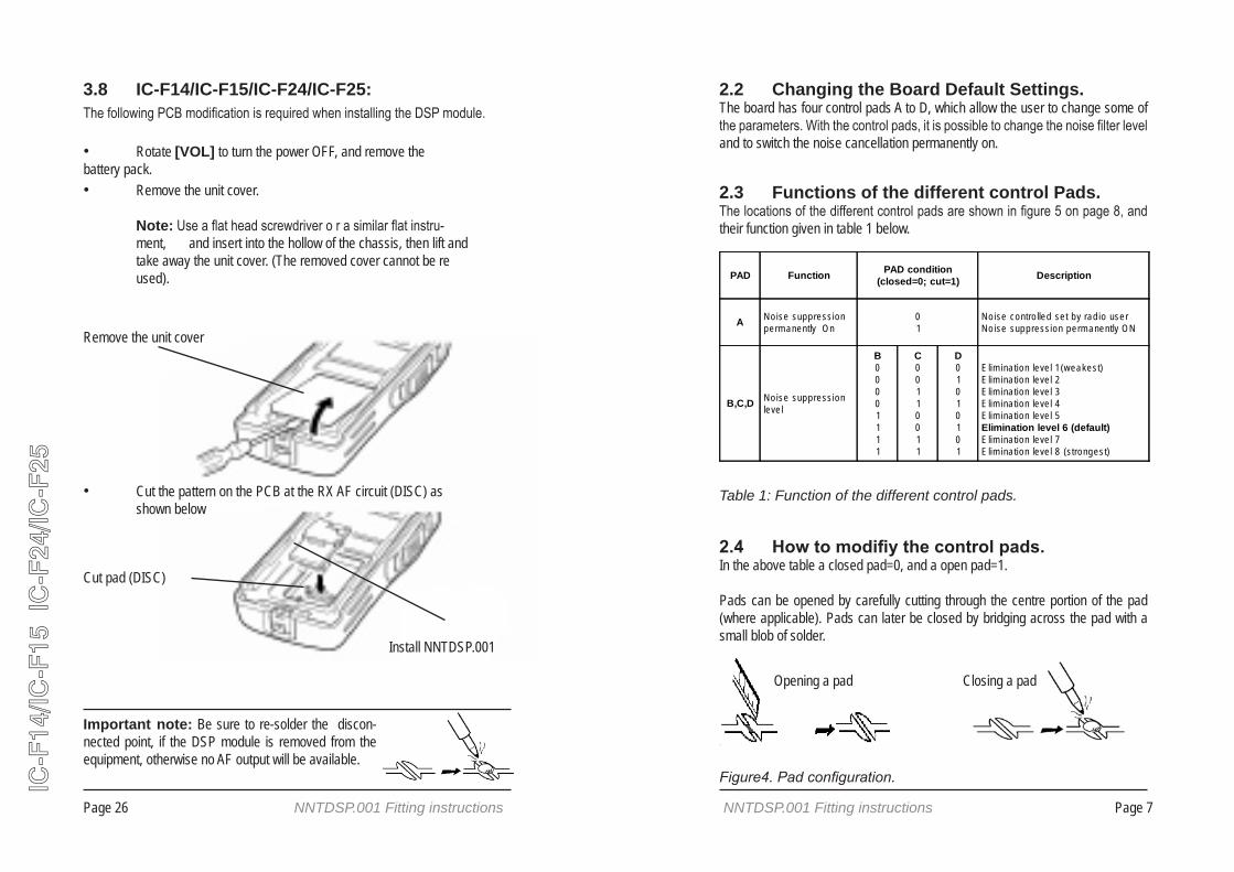
3.9 IC-F33/F34 F43/F44GT/GS:
• Cut the pattern on the PCB at the RX AF circuit (DISC) as shown below
Remove the unit cover
Cut pad (DISC)
Install NNTDSP.001
The following PCB modification is required when installing the DSP module.
• Rotate [VOL] to turn the power OFF, and remove the battery pack.• Remove the unit cover.
Note: Use a flat head screwdriver o r a similar flat instrument, and insert into the hollow of the chassis, then lift and take away the unit cover. Use the supplied spare unit cover. Do not use the cover that has been removed. Water of dust may get into the transceiver because the cover may be bent or has lost it’s adhesion. This may result in the transceiver becom ing damaged.
NNTDSP.001 Fitting instructionsNNTDSP.001 Fitting instructions Page 7
2.2 Changing the Board Default Settings.The board has four control pads A to D, which allow the user to change some of the parameters. With the control pads, it is possible to change the noise filter level and to switch the noise cancellation permanently on.
Table 1: Function of the different control pads.
2.3 Functions of the different control Pads. The locations of the different control pads are shown in figure 5 on page 8, and their function given in table 1 below.
2.4 Howtomodifiythecontrolpads.In the above table a closed pad=0, and a open pad=1.
Pads can be opened by carefully cutting through the centre portion of the pad (where applicable). Pads can later be closed by bridging across the pad with a small blob of solder.
Opening a pad Closing a pad
Figure4. Pad configuration.
PAD Function PAD condition(closed=0; cut=1) Description
A No ise supp ress ionpe rm anently On
01
No ise contro lled se t by rad io use rNo ise supp ress ion pe rm anently ON
B,C,D No ise supp ress ionleve l
B00001111
C00110011
D01010101
E lim ina tion leve l 1 (weakest)E lim ina tion leve l 2E lim ina tion leve l 3E lim ina tion leve l 4E lim ina tion leve l 5Elimination level 6 (default)E lim ina tion leve l 7E lim ina tion leve l 8 (s trongest)
Page 26
IC-F
14/IC
-F15
IC
-F24
/IC-F
25
3.8 IC-F14/IC-F15/IC-F24/IC-F25:The following PCB modification is required when installing the DSP module.
• Rotate [VOL] to turn the power OFF, and remove the battery pack.• Remove the unit cover.
Note: Use a flat head screwdriver o r a similar flat instru- ment, and insert into the hollow of the chassis, then lift and take away the unit cover. (The removed cover cannot be re used).
• Cut the pattern on the PCB at the RX AF circuit (DISC) as shown below
Remove the unit cover
Cut pad (DISC)
Important note: Be sure to re-solder the discon-nected point, if the DSP module is removed from the equipment, otherwise no AF output will be available.
Install NNTDSP.001
NNTDSP.001 Fitting instructionsNNTDSP.001 Fitting instructionsPage 8
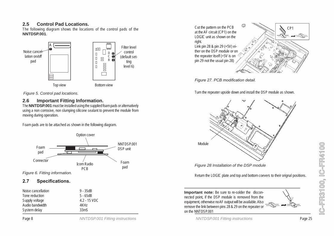
2.5 Control Pad Locations.The following diagram shows the locations of the control pads of the NNTDSP.001.
Figure 5. Control pad locations.
Top view Bottom view
Figure 6. Fitting information.
2.6 Important Fitting Information.The NNTDSP.001 must be installed using the supplied foam pads or alternatively using a non corrosive, non slumping silicone sealant to prevent the module from moving during operation.
Foam pads are to be attached as shown in the following diagram.
2.7 Specifications.
Noise cancellation 9 - 35dBTone reduction 5 - 65dBSupply voltage 4.2 - 15 VDCAudio bandwidth 4KHzSystem delay 33mS
Filter level control
(default set-ting
level 6)
DCB
ANoise cancel-lation on/off
pad
Icom Radio PCB
NNTDSP.001DSP unit
Foam pad
Foam pad
Option cover
Connector
Page 25
Important note: Be sure to re-solder the discon-nected point, if the DSP module is removed from the equipment, otherwise no AF output will be available. Also remove the link between pins 28 & 29 on the repeater or on the NNTDSP.001 IC
-FR
3100
, IC
-FR
4100
Figure 27. PCB modification detail.
Turn the repeater upside down and install the DSP module as shown.
Figure 28 Installation of the DSP module
Return the LOGIC plate and top and bottom coevers to their orignal positions.
Cut the pattern on the PCB at the AF circuit (CP1) on the LOGIC unit as shown on the right. Link pin 28 & pin 29 (+5V) ei-ther on the DSP module or on the repeater itself (+5V is on pin 29 not the usual pin 28)
CP1
Module

NNTDSP.001 Fitting instructionsNNTDSP.001 Fitting instructions Page 9
Figure 7. Physical dimensions of the NNTDSP.001 module.
34.5 mm
21 mm5.5 mm
2.9 Physical dimensions.
2.8 Connector Pin-out.The following table identifies the pin-out of the NNTDSP.001 module connec-tor.
Table 2. NNTDSP.001 connector pin-out.
A
Top view of connector
16 15
30 1
Overal height
Pin Signal Remark
6 B usy/P ower On low = on, high = o ff
9 No ise F ilte r On/O ff low = o ff, high = on
22 S igna l out F rom Icom boa rd
23 S igna l in To Icom boa rd
28 +V S upp ly
30 Ground
Page 24
3.7 IC-FR3100, IC-FR4100 Repeaters
IC-F
R31
00, I
C-F
R41
00
Figure 25. Repeater case disassembly detail.
Figure 26. Remove the logic plate.
Case opening procedure.
CAUTION: DISCONNECT the AC power cable and/or DC power cable from the repeater. Other-wise, there is danger of electric shock and/or equipmentdamage.
• Remove 6 screws from the top of the repeater and 4 screws from the sides, then lift up the top cover.• Turn the repeater upside down.• Remove 6 screws from the bottom of the repeater, and 4 screws from the sides, then lift up the bottom
DSP module installation.Remove the 8 screws from the LOGIC shielding plate, then remove the cover.
NNTDSP.001 Fitting instructionsNNTDSP.001 Fitting instructionsPage 10
B
Rear
AntIC-F300/S series.
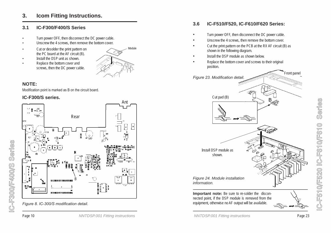
3. Icom Fitting Instructions.
Figure 8. IC-300/S modification detail.
• Cut or desolder the print pattern on the PC board at the AF circuit (B).• Install the DSP unit as shown.• Replace the bottom cover and screws, then the DC power cable.
NOTE:Modification point is marked as B on the circuit board.
3.1 IC-F300/F400/S Series
• Turn power OFF, then disconnect the DC power cable.• Unscrew the 4 screws, then remove the bottom cover.
IC-F
300/
F40
0/S
Ser
ies
Module
Page 23
3.6 IC-F510/F520, IC-F610/F620 Series:
Cut pad (B)
• Turn power OFF, then disconnect the DC power cable.• Unscrew the 4 screws, then remove the bottom cover.• Cut the print pattern on the PCB at the RX AF circuit (B) as shown in the following diagram.• Install the DSP module as shown below.• Replace the bottom cover and screws to their original position.
Install DSP module as shown.
Front panelFigure 23. Modification detail.
Figure 24. Module installation information.
IC-F
510/
F52
0 IC
-F61
0/F
610
Ser
ies
Important note: Be sure to re-solder the discon-nected point, if the DSP module is removed from the equipment, otherwise no AF output will be available.

NNTDSP.001 Fitting instructionsNNTDSP.001 Fitting instructions Page 11
IC-F400/S series.
Figure 9. IC-400/S modification detail.
B
Important note: Be sure to re-solder the discon-nected point, if the DSP module is removed from the equipment, otherwise no AF output will be available.
NOTE:Modification point is marked as B on the circuit board.
IC-F
400/
S S
erie
s
• Cut or desolder the print pattern on the PC board at the AF circuit (B).• Install the DSP unit as shown on the previous page.• Replace the bottom cover and screws, then the DC power cable.
• Turn power OFF, then disconnect the DC power cable.• Unscrew the 4 screws, then remove the bottom cover.
RearAnt
Page 22
IC-F30/F31GT/GS, F40/F41GT/GS Series:
Cut the junction pattern A (AF line) on the MAIN unit.
OPT2OPT1
MAIN unitFigure 22. Module installation information.
IC-F
30/3
1GT
/GS
IC-F
40/F
41/G
T/G
S S
erie
s
Important note: Be sure to re-solder the discon-nected point, if the DSP module is removed from the equipment, otherwise no AF output will be available.
AF line

NNTDSP.001 Fitting instructionsNNTDSP.001 Fitting instructionsPage 12
Fitting procedure:Refere to figure 10.
• Remove the knob and unscrew the antenna connector screw.• Unscrew the 2 screws, then remove the front panel.• Remove the shield cover if necessary.• Remove the jumper chip (DET)*2 or (AF)*2 on the• LCD side of the PC board.• Replace the shield cover to the original position.• Remove the jumper chip resistor(s) on the CPU side• of the PC board.• Install the unit as shown in the instruction manual.• Replace the front panel and screws.
NOTE:*1 B4929F and B4923H’s modification points may be accessed through the service window without taking the unit apart.*2 Modification points are marked DET or AF on the main board.
3.2 IC-F3/F4/S series.
IC-F3/F4/S seriesThere are 2 types of printed circuit board fitted to this series. Be sure to confirm the board type number in advance. The board number is printed on the PCB.
IC-F3/IC-F3S• B4929E requires LCD side and CPU side modifications.• B4929F*1 requires CPU side only.
IC-F4/IC-F4S• B4923G LCD side and CPU side modifications.• B4923H*1 requires CPU side only.
IC-F
3/F
4/S
Ser
ies
Page 21
3.5 IC-F30/F31GT/GS IC-F40/F41GT/GS Series
Disassemble the unit as described below before fitting the DSP module.
• Unscrew nut (a), and remove the knobs.• Unscrew screw (b) and 2 screws (c), then remove the multi- connector cover and rear panel.• Unscrew 2 screws (d), then remove the multi-connector.• Unscrew 2 screws (e), then take off the chassis front the front panel in the direction of the arrow.• Warning: Flat cable is connected between the MAIN unit on the chassis and the front panel.• Install the DSP module in OPT1.
Figure 21. Module installation information.
IC-F
30/3
1GT
/GS
IC-F
40/F
41/G
T/G
S S
erie
s

NNTDSP.001 Fitting instructionsNNTDSP.001 Fitting instructions Page 13
Figure 10. IC-F3/F4/S series dismantling procedure.
IC-F
3/F
4/S
Ser
ies
Important note: Be sure to re-solder the discon-nected point, if the DSP module is removed from the equipment, otherwise no AF output will be available.
Figure 11. NNTDSP.001 installation.
• Remove the service cover.• Take out the protective sponge.• This sponge is not used when options are installed.• Connect the optional unit as shown.• Replace the service cover.
Page 20
3.4 IC-F1010/F1020/F2010/F2020 Series
• Cut the junction AFO on the main board.• Install the unit as shown in the diagram on the right.• Replace the bottom cover and screws, then the DC power cable.
NNTDSP.001
MAIN unitFRONT
AFO
• Turn power OFF, then disconnect the DC power cable.• Unscrew the 4 screws, then remove the bottom cover.
Figure 19. Module installation
Figure 20. Main unit modification point.
IC-F
1010
/F10
20/F
2010
/F20
20 S
erie
s
Important note: Be sure to re-solder the discon-nected point, if the DSP module is removed from the equipment, otherwise no AF output will be available.
Module

NNTDSP.001 Fitting instructionsNNTDSP.001 Fitting instructionsPage 14
SpeakerSP1
DETRemove this resistor
Antenna
Micro
phon
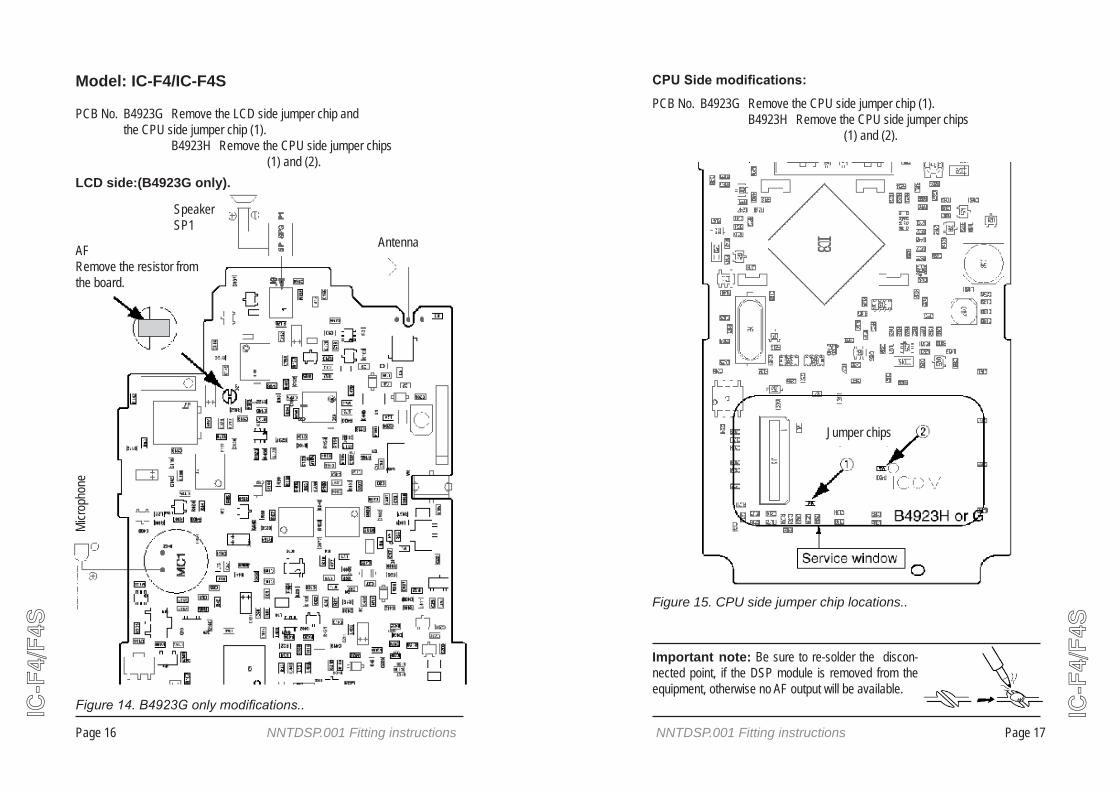
eModel: IC-F3/IC-F3S
PCB No. B4929E Remove the LCD side jumper chip and the CPU side jumper chip (1). B4929F Remove the CPU side jumper chips (1) and (2).LCD side:( B4929E only).
Figure 12. B4929E modification detail.IC-F
3/F
3S
Page 19
IC-F4GT/IC-F4GS
CF
Service window
Cut the junction pattern F on the PC board.
Figure 18. IC-F4GT/GS modification detail..
IC-F
4GT
/GS
Important note: Be sure to re-solder the discon-nected point, if the DSP module is removed from the equipment, otherwise no AF output will be available.
NNTDSP.001 Fitting instructionsNNTDSP.001 Fitting instructions Page 15
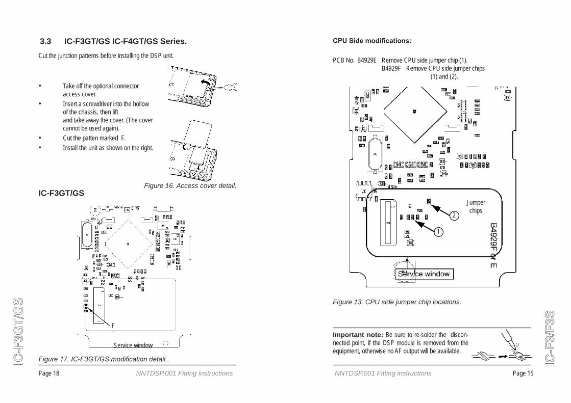
CPUSidemodifications:
Figure 13. CPU side jumper chip locations.
PCB No. B4929E Remove CPU side jumper chip (1). B4929F Remove CPU side jumper chips (1) and (2).
Jumperchips2
1
IC-F
3/F
3S
Important note: Be sure to re-solder the discon-nected point, if the DSP module is removed from the equipment, otherwise no AF output will be available.
Page 18
FService window
3.3 IC-F3GT/GS IC-F4GT/GS Series.
• Take off the optional connector access cover.• Insert a screwdriver into the hollow of the chassis, then lift and take away the cover. (The cover cannot be used again).• Cut the patten marked F.• Install the unit as shown on the right.
Cut the junction patterns before installing the DSP unit.
IC-F3GT/GSFigure 16. Access cover detail.
Figure 17. IC-F3GT/GS modification detail..IC-F
3GT
/GS
F
NNTDSP.001 Fitting instructionsNNTDSP.001 Fitting instructionsPage 16
Model: IC-F4/IC-F4S
PCB No. B4923G Remove the LCD side jumper chip and the CPU side jumper chip (1). B4923H Remove the CPU side jumper chips (1) and (2).LCD side:(B4923G only).
AFRemove the resistor from the board.
SpeakerSP1
Antenna
Micro
phon
e
Figure 14. B4923G only modifications..IC-F
4/F
4S
Page 17
CPUSidemodifications:
2
1
Figure 15. CPU side jumper chip locations..
PCB No. B4923G Remove the CPU side jumper chip (1). B4923H Remove the CPU side jumper chips (1) and (2).
Jumper chips
IC-F
4/F
4S
Important note: Be sure to re-solder the discon-nected point, if the DSP module is removed from the equipment, otherwise no AF output will be available.


