1024-Bit EEPROM iButton DS1972 - Maxim Integrated · Note 25: EEPROM writes can become...
23
DS1972 1024-Bit EEPROM i Button ________________________________________________________________ Maxim Integrated Products 1 19-4888; Rev 4; 1/12 For pricing, delivery, and ordering information, please contact Maxim Direct at 1-888-629-4642, or visit Maxim’s website at www.maxim-ic.com. General Description The DS1972 is a 1024-bit, 1-Wire ® EEPROM chip orga- nized as four memory pages of 256 bits each in a rugged i Button ® package. Data is written to an 8-byte scratchpad, verified, and then copied to the EEPROM memory. As a special feature, the four memory pages can individually be write protected or put in EPROM- emulation mode, where bits can only be changed from a 1 to a 0 state. The DS1972 communicates over the single-conductor 1-Wire bus. The communication fol- lows the standard 1-Wire protocol. Each device has its own unalterable and unique 64-bit ROM registration number that is factory lasered into the device. The reg- istration number is used to address the device in a mul- tidrop, 1-Wire net environment. Applications Access Control/Parking Meter Work-in-Progress Tracking Tool Management Inventory Control Maintenance/Inspection Data Storage Features ♦ 1024 Bits of EEPROM Memory Partitioned Into Four Pages of 256 Bits ♦ Individual Memory Pages Can Be Permanently Write Protected or Put in EPROM-Emulation Mode (“Write to 0”) ♦ Switchpoint Hysteresis and Filtering to Optimize Performance in the Presence of Noise ♦ IEC 1000-4-2 Level 4 ESD Protection (±8kV Contact, ±15kV Air, Typical) ♦ Reads and Writes Over a Wide Voltage Range from 2.8V to 5.25V from -40°C to +85°C ♦ Communicates to Host with a Single Digital Signal at 15.4kbps or 125kbps Using 1-Wire Protocol Common i Button Features ♦ Unique Factory-Lasered 64-Bit Registration Number Ensures Error-Free Device Selection and Absolute Traceability Because No Two Parts are Alike ♦ Built-In Multidrop Controller for 1-Wire Net ♦ Chip-Based Data Carrier Stores Digital Identification and Information, Armored in a Durable Stainless-Steel Case ♦ Data Can Be Accessed While Affixed to Object ♦ Button Shape is Self-Aligning with Cup-Shaped Probes ♦ Easily Affixed with Self-Stick Adhesive Backing, Latched by its Flange, or Locked with a Ring Pressed Onto its Rim ♦ Presence Detector Acknowledges When Reader First Applies Voltage Ordering Information 16.25mm 5.89mm 0.51mm 3.10mm 0.51mm 17.35mm BRANDING F5 SIZE GND GND IO IO F3 SIZE 52 2D 0000006234FB 1-Wire ® ® i B u t t o n ® . c o m Y Y W W Z Z Z D S 1 9 7 2 - F 5 Pin Configurations +Denotes a lead(Pb)-free/RoHS-compliant package. PART TEMP RANGE PIN-PACKAGE DS1972-F5+ -40°C to +85°C F5 i Button DS1972-F3+ -40°C to +85°C F3 i Button Examples of Accessories PART ACCESSORY DS9096P Self-Stick Adhesive Pad DS9101 Multipurpose Clip DS9093RA Mounting Lock Ring DS9093A Snap-In Fob DS9092 i Button Probe 1-Wire and i Button are registered trademarks of Maxim Integrated Products, Inc.
Transcript of 1024-Bit EEPROM iButton DS1972 - Maxim Integrated · Note 25: EEPROM writes can become...

DS
19
72
1024-Bit EEPROM iButton
________________________________________________________________ Maxim Integrated Products 1
19-4888; Rev 4; 1/12
For pricing, delivery, and ordering information, please contact Maxim Direct at 1-888-629-4642,or visit Maxim’s website at www.maxim-ic.com.
General DescriptionThe DS1972 is a 1024-bit, 1-Wire® EEPROM chip orga-nized as four memory pages of 256 bits each in arugged iButton® package. Data is written to an 8-bytescratchpad, verified, and then copied to the EEPROMmemory. As a special feature, the four memory pagescan individually be write protected or put in EPROM-emulation mode, where bits can only be changed froma 1 to a 0 state. The DS1972 communicates over thesingle-conductor 1-Wire bus. The communication fol-lows the standard 1-Wire protocol. Each device has itsown unalterable and unique 64-bit ROM registrationnumber that is factory lasered into the device. The reg-istration number is used to address the device in a mul-tidrop, 1-Wire net environment.
ApplicationsAccess Control/Parking Meter
Work-in-Progress Tracking
Tool Management
Inventory Control
Maintenance/Inspection Data Storage
Features♦ 1024 Bits of EEPROM Memory Partitioned Into
Four Pages of 256 Bits
♦ Individual Memory Pages Can Be PermanentlyWrite Protected or Put in EPROM-Emulation Mode(“Write to 0”)
♦ Switchpoint Hysteresis and Filtering to OptimizePerformance in the Presence of Noise
♦ IEC 1000-4-2 Level 4 ESD Protection (±8kVContact, ±15kV Air, Typical)
♦ Reads and Writes Over a Wide Voltage Rangefrom 2.8V to 5.25V from -40°C to +85°C
♦ Communicates to Host with a Single DigitalSignal at 15.4kbps or 125kbps Using 1-WireProtocol
Common iButton Features♦ Unique Factory-Lasered 64-Bit Registration
Number Ensures Error-Free Device Selection andAbsolute Traceability Because No Two Parts areAlike
♦ Built-In Multidrop Controller for 1-Wire Net
♦ Chip-Based Data Carrier Stores DigitalIdentification and Information, Armored in aDurable Stainless-Steel Case
♦ Data Can Be Accessed While Affixed to Object
♦ Button Shape is Self-Aligning with Cup-ShapedProbes
♦ Easily Affixed with Self-Stick Adhesive Backing,Latched by its Flange, or Locked with a RingPressed Onto its Rim
♦ Presence Detector Acknowledges When ReaderFirst Applies Voltage
Ordering Information
16.25mm
5.89mm0.51mm
3.10mm
0.51mm
17.35mm
BRANDING
F5 SIZE
GNDGNDIOIO
F3 SIZE
52 2D0000006234FB
1-Wire®
®
i B
u t t o n®. c o m
YYWW ZZZ DS1972-F5
Pin Configurations
+Denotes a lead(Pb)-free/RoHS-compliant package.
PART TEMP RANGE PIN-PACKAGE
DS1972-F5+ -40°C to +85°C F5 iButton
DS1972-F3+ -40°C to +85°C F3 iButton
Examples of AccessoriesPART ACCESSORY
DS9096P Self-Stick Adhesive Pad
DS9101 Multipurpose Clip
DS9093RA Mounting Lock Ring
DS9093A Snap-In Fob
DS9092 iButton Probe
1-Wire and iButton are registered trademarks of MaximIntegrated Products, Inc.

DS
19
72
1024-Bit EEPROM iButton
2 _______________________________________________________________________________________
ABSOLUTE MAXIMUM RATINGS
ELECTRICAL CHARACTERISTICS(TA = -40°C to +85°C, unless otherwise noted.) (Note 1)
Stresses beyond those listed under “Absolute Maximum Ratings” may cause permanent damage to the device. These are stress ratings only, and functionaloperation of the device at these or any other conditions beyond those indicated in the operational sections of the specifications is not implied. Exposure toabsolute maximum rating conditions for extended periods may affect device reliability.
IO Voltage Range to GND .......................................-0.5V to +6VIO Sink Current ...................................................................20mAOperating Temperature Range ...........................-40°C to +85°C
Junction Temperature ......................................................+150°CStorage Temperature Range .............................-55°C to +125°C
PARAMETER SYMBOL CONDITIONS MIN TYP MAX UNITS
IO PIN: GENERAL DATA
1-Wire Pullup Voltage VPUP (Note 2) 2.8 5.25 V
1-Wire Pullup Resistance RPUP (Notes 2, 3) 0.3 2.2 k
Input Capacitance CIO (Notes 4, 5) 1000 pF
Input Load Current IL IO pin at VPUP 0.05 6.7 μA
High-to-Low Switching Threshold VTL (Notes 5, 6, 7) 0.5 VPUP -
1.8 V
Input Low Voltage VIL (Notes 2, 8) 0.5 V
Low-to-High Switching Threshold VTH (Notes 5, 6, 9) 1.0 VPUP -
1.0 V
Switching Hysteresis VHY (Notes 5, 6, 10) 0.21 1.70 V
Output Low Voltage VOL At 4mA (Note 11) 0.4 V
Standard speed, RPUP = 2.2k 5
Overdrive speed, RPUP = 2.2k 2 Recovery Time (Notes 2, 12)
tREC Overdrive speed, directly prior to reset pulse; RPUP = 2.2k
5
μs
Standard speed 0.5 5.0 Rising-Edge Hold-Off Time (Notes 5, 13)
tREH Overdrive speed Not applicable (0)
μs
Standard speed 65 Time Slot Duration (Notes 2, 14)
tSLOT Overdrive speed 8
μs
IO PIN: 1-Wire RESET, PRESENCE-DETECT CYCLE
Standard speed 480 640 Reset Low Time (Note 2) tRSTL
Overdrive speed 48 80 μs
Standard speed 15 60 Presence-Detect High Time tPDH
Overdrive speed 2 6 μs
Standard speed 60 240 Presence-Detect Low Time tPDL
Overdrive speed 8 24 μs
Standard speed 60 75 Presence-Detect Sample Time (Notes 2, 15)
tMSPOverdrive speed 6 10
μs

DS
19
72
1024-Bit EEPROM iButton
_______________________________________________________________________________________ 3
ELECTRICAL CHARACTERISTICS (continued)(TA = -40°C to +85°C, unless otherwise noted.) (Note 1)
PARAMETER SYMBOL CONDITIONS MIN TYP MAX UNITS
IO PIN: 1-Wire WRITE
Standard speed 60 120
Overdrive speed, VPUP > 4.5V 5 15.5 Write-Zero Low Time (Notes 2, 16, 17)
tW0L
Overdrive speed 6 15.5
μs
Standard speed 1 15 Write-One Low Time (Notes 2, 17)
tW1L Overdrive speed 1 2
μs
IO PIN: 1-Wire READ
Standard speed 5 15 - Read Low Time (Notes 2, 18)
tRL Overdrive speed 1 2 -
μs
Standard speed tRL + 15 Read Sample Time (Notes 2, 18)
tMSROverdrive speed tRL + 2
μs
EEPROM
Programming Current IPROG (Notes 5, 19) 0.8 mA
Programming Time tPROG (Note 20) 10 ms
At +25°C 200k Write/Erase Cycles (Endurance) (Notes 21, 22)
NCY At +85°C (worst case) 50k
Data Retention (Notes 23, 24, 25)
tDR At +85°C (worst case) 40 Years
Note 1: Limits are 100% production tested at TA = +25°C and/or TA = +85°C. Limits over the operating temperature range and rel-evant supply voltage range are guaranteed by design and characterization. Typical values are not guaranteed.
Note 2: System requirement.Note 3: Maximum allowable pullup resistance is a function of the number of 1-Wire devices in the system and 1-Wire recovery times.
The specified value here applies to systems with only one device and with the minimum 1-Wire recovery times. For moreheavily loaded systems, an active pullup such as that found in the DS2482-x00, DS2480B, or DS2490 may be required.
Note 4: Maximum value represents the internal parasite capacitance when VPUP is first applied. If a 2.2kΩ resistor is used to pullup the data line, 2.5µs after VPUP has been applied, the parasite capacitance does not affect normal communications.
Note 5: Guaranteed by design, characterization, and/or simulation only. Not production tested.Note 6: VTL, VTH, and VHY are a function of the internal supply voltage, which is a function of VPUP, RPUP, 1-Wire timing, and
capacitive loading on IO. Lower VPUP, higher RPUP, shorter tREC, and heavier capacitive loading all lead to lower values ofVTL, VTH, and VHY.
Note 7: Voltage below which, during a falling edge on IO, a logic 0 is detected.Note 8: The voltage on IO must be less than or equal to VILMAX at all times the master is driving IO to a logic 0 level.Note 9: Voltage above which, during a rising edge on IO, a logic 1 is detected.Note 10: After VTH is crossed during a rising edge on IO, the voltage on IO must drop by at least VHY to be detected as logic 0.Note 11: The I-V characteristic is linear for voltages less than 1V.Note 12: Applies to a single device attached to a 1-Wire line.Note 13: The earliest recognition of a negative edge is possible at tREH after VTH has been reached on the preceding rising edge.Note 14: Defines maximum possible bit rate. Equal to tW0LMIN + tRECMIN.Note 15: Interval after tRSTL during which a bus master is guaranteed to sample a logic 0 on IO if there is a DS1972 present.
Minimum limit is tPDHMAX; maximum limit is tPDHMIN + tPDLMIN.Note 16: Numbers in bold are not in compliance with legacy 1-Wire product standards. See the Comparison Table.Note 17: ε in Figure 11 represents the time required for the pullup circuitry to pull the voltage on IO up from VIL to VTH. The actual
maximum duration for the master to pull the line low is tW1LMAX + tF - ε and tW0LMAX + tF - ε, respectively.Note 18: δ in Figure 11 represents the time required for the pullup circuitry to pull the voltage on IO up from VIL to the input-high
threshold of the bus master. The actual maximum duration for the master to pull the line low is tRLMAX + tF.

DS
19
72
1024-Bit EEPROM iButton
4 _______________________________________________________________________________________
Note 19: Current drawn from IO during the EEPROM programming interval. The pullup circuit on IO during the programming intervalshould be such that the voltage at IO is greater than or equal to VPUPMIN. If VPUP in the system is close to VPUPMIN, a low-impedance bypass of RPUP, which can be activated during programming, may need to be added.
Note 20: Interval begins tREHMAX after the trailing rising edge on IO for the last time slot of the E/S byte for a valid Copy Scratchpadsequence. Interval ends once the device’s self-timed EEPROM programming cycle is complete and the current drawn bythe device has returned from IPROG to IL.
Note 21: Write-cycle endurance is degraded as TA increases.Note 22: Not 100% production tested; guaranteed by reliability monitor sampling.Note 23: Data retention is degraded as TA increases.Note 24: Guaranteed by 100% production test at elevated temperature for a shorter time; equivalence of this production test to the
data sheet limit at operating temperature range is established by reliability testing.Note 25: EEPROM writes can become nonfunctional after the data-retention time is exceeded. Long-term storage at elevated tem-
peratures is not recommended; the device can lose its write capability after 10 years at +125°C or 40 years at +85°C.
COMPARISON TABLELEGACY VALUES DS1972 VALUES
STANDARD SPEED (μs)
OVERDRIVE SPEED (μs)
STANDARD SPEED (μs)
OVERDRIVE SPEED (μs)
PARAMETER
MIN MAX MIN MAX MIN MAX MIN MAX
tSLOT (including tREC) 61 (undefined) 7 (undefined) 65* (undefined) 8* (undefined)
tRSTL 480 (undefined) 48 80 480 640 48 80
tPDH 15 60 2 6 15 60 2 6
tPDL 60 240 8 24 60 240 8 24
tW0L 60 120 6 16 60 120 6 15.5
*Intentional change; longer recovery time requirement due to modified 1-Wire front-end.
Note: Numbers in bold are not in compliance with legacy 1-Wire product standards.

DS
19
72
1024-Bit EEPROM iButton
_______________________________________________________________________________________ 5
Detailed DescriptionThe DS1972 combines 1024 bits of EEPROM, an 8-byte register/control page with up to 7 user read/writebytes, and a fully featured 1-Wire interface in a ruggediButton package. Each DS1972 has its own 64-bit ROMregistration number that is factory lasered into the chipto provide a guaranteed unique identity for absolutetraceability. Data is transferred serially through the 1-Wire protocol, which requires only a single data contactand a ground return. The DS1972 has an additionalmemory area called the scratchpad that acts as abuffer when writing to the main memory or the registerpage. Data is first written to the scratchpad from whichit can be read back. After the data has been verified, aCopy Scratchpad command transfers the data to itsfinal memory location. Applications of the DS1972include access control/parking meter, work-in-progresstracking, tool management, inventory control, andmaintenance/inspection data storage. Free software forcommunication with the DS1972 is available atwww.maxim-ic.com/ibutton.
OverviewThe block diagram in Figure 1 shows the relationshipsbetween the major control and memory sections of theDS1972. The DS1972 has four main data components:64-bit lasered ROM, 64-bit scratchpad, four 32-bytepages of EEPROM, and a 64-bit register page.
The hierarchical structure of the 1-Wire protocol isshown in Figure 2. The bus master must first provideone of the seven ROM function commands: ReadROM, Match ROM, Search ROM, Skip ROM, Resume,Overdrive-Skip ROM, or Overdrive-Match ROM. Upon
completion of an Overdrive-Skip ROM or Overdrive-Match ROM command byte executed at standardspeed, the device enters overdrive mode where allsubsequent communication occurs at a higherspeed. The protocol required for these ROM function
MEMORYFUNCTION
CONTROL UNIT
DATA MEMORY4 PAGES OF
256 BITS EACH
CRC-16GENERATOR
64-BITSCRATCHPAD
1-WireFUNCTION CONTROL
64-BITLASERED ROM
PARASITE POWER
IO
REGISTER PAGE64 BITS
DS1972
Figure 1. Block Diagram
DS1972 COMMAND LEVEL:
AVAILABLE COMMANDS: DATA FIELD AFFECTED:
READ ROMMATCH ROMSEARCH ROMSKIP ROMRESUMEOVERDRIVE-SKIP ROMOVERDRIVE-MATCH ROM
64-BIT REG. #, RC-FLAG64-BIT REG. #, RC-FLAG64-BIT REG. #, RC-FLAGRC-FLAGRC-FLAGRC-FLAG, OD-FLAG64-BIT REG. #, RC-FLAG, OD-FLAG
1-Wire ROM FUNCTION COMMANDS(SEE FIGURE 9)
WRITE SCRATCHPADREAD SCRATCHPADCOPY SCRATCHPADREAD MEMORY
64-BIT SCRATCHPAD, FLAGS64-BIT SCRATCHPADDATA MEMORY, REGISTER PAGEDATA MEMORY, REGISTER PAGE
DS1972-SPECIFICMEMORY FUNCTION COMMANDS
(SEE FIGURE 7)
Figure 2. Hierarchical Structure for 1-Wire Protocol

DS
19
72
1024-Bit EEPROM iButton
6 _______________________________________________________________________________________
1STSTAGE
2NDSTAGE
3RDSTAGE
4THSTAGE
7THSTAGE
8THSTAGE
6THSTAGE
5THSTAGE
X0 X1 X2 X3 X4
POLYNOMIAL = X8 + X5 + X4 + 1
INPUT DATA
X5 X6 X7 X8
Figure 4. 1-Wire CRC Generator
commands is described in Figure 9. After a ROMfunction command is successfully executed, thememory functions become accessible and the mastercan provide any one of the four memory functioncommands. The protocol for these memory functioncommands is described in Figure 7. All data is readand written least significant bit first.
64-Bit Lasered ROMEach DS1972 contains a unique ROM code that is 64bits long. The first 8 bits are a 1-Wire family code. Thenext 48 bits are a unique serial number. The last 8 bitsare a cyclic redundancy check (CRC) of the first 56 bits.See Figure 3 for details. The 1-Wire CRC is generated
using a polynomial generator consisting of a shift regis-ter and XOR gates as shown in Figure 4. The polynomialis X8 + X5 + X4 + 1. Additional information about the 1-Wire CRC is available in Application Note 27:Understanding and Using Cyclic Redundancy Checkswith Maxim iButton Products.
The shift register bits are initialized to 0. Then, startingwith the least significant bit of the family code, one bitat a time is shifted in. After the 8th bit of the family codehas been entered, the serial number is entered. Afterthe last bit of the serial number has been entered, theshift register contains the CRC value. Shifting in the 8bits of the CRC returns the shift register to all 0s.
MSB
8-BITCRC CODE 48-BIT SERIAL NUMBER
MSB MSBLSB
LSB
LSB
8-BIT FAMILY CODE(2Dh)
MSBLSB
Figure 3. 64-Bit Lasered ROM

DS
19
72
1024-Bit EEPROM iButton
_______________________________________________________________________________________ 7
Memory AccessData memory and registers are located in a linearaddress space, as shown in Figure 5. The data memoryand the registers have unrestricted read access. TheDS1972 EEPROM array consists of 18 rows of 8 byteseach. The first 16 rows are divided equally into fourmemory pages (32 bytes each). These four pages arethe primary data memory. Each page can be individu-ally set to open (unprotected), write protected, orEPROM mode by setting the associated protection bytein the register row. As a factory default, the entire datamemory is unprotected and its contents are undefined.The last two rows contain protection registers andreserved bytes. The register row consists of 4 protec-tion-control bytes, a copy-protection byte, the factorybyte, and 2 user byte/manufacture ID bytes. The manu-facturer ID can be a customer-supplied identification
code that assists the application software in identifyingthe product with which the DS1972 is associated.Contact the factory to set up and register a custommanufacturer ID. The last row is reserved for future use.It is undefined in terms of R/W functionality and shouldnot be used.
In addition to the main EEPROM array, an 8-bytevolatile scratchpad is included. Writes to the EEPROMarray are a two-step process. First, data is written to thescratchpad and then copied into the main array. Thisallows the user to first verify the data written to thescratchpad prior to copying into the main array. Thedevice only supports full row (8-byte) copy operations.For data in the scratchpad to be valid for a copy opera-tion, the address supplied with a Write Scratchpadcommand must start on a row boundary, and 8 fullbytes must be written into the scratchpad.
ADDRESS RANGE TYPE DESCRIPTION PROTECTION CODES
0000h to 001Fh R/(W) Data Memory Page 0 —
0020h to 003Fh R/(W) Data Memory Page 1 —
0040h to 005Fh R/(W) Data Memory Page 2 —
0060h to 007Fh R/(W) Data Memory Page 3 —
0080h* R/(W) Protection-Control Byte Page 0 55h: Write Protect P0; AAh: EPROM Mode P0; 55h or AAh: Write Protect 80h
0081h* R/(W) Protection-Control Byte Page 1 55h: Write Protect P1; AAh: EPROM Mode P1; 55h or AAh: Write Protect 81h
0082h* R/(W) Protection-Control Byte Page 2 55h: Write Protect P2; AAh: EPROM Mode P2; 55h or AAh: Write Protect 82h
0083h* R/(W) Protection-Control Byte Page 3 55h: Write Protect P3; AAh: EPROM Mode P3; 55h or AAh: Write Protect 83h
0084h* R/(W) Copy Protection Byte 55h or AAh: Copy Protect 0080h:008Fh, and Any Write-Protected Pages
0085h R Factory Byte. Set at Factory. AAh: Write Protect 85h, 86h, 87h; 55h: Write Protect 85h; Unprotect 86h, 87h
0086h R/(W) User Byte/Manufacturer ID —
0087h R/(W) User Byte/Manufacturer ID —
0088h to 008Fh — Reserved —
Figure 5. Memory Map
*Once programmed to AAh or 55h this address becomes read only. All other codes can be stored, but neither write protect theaddress nor activate any function.

DS
19
72
1024-Bit EEPROM iButton
8 _______________________________________________________________________________________
The protection-control registers determine how incom-ing data on a Write Scratchpad command is loadedinto the scratchpad. A protection setting of 55h (writeprotect) causes the incoming data to be ignored andthe target address main memory data to be loaded intothe scratchpad. A protection setting of AAh (EPROMmode) causes the logical AND of incoming data andtarget address main memory data to be loaded into thescratchpad. Any other protection-control register set-ting leaves the associated memory page open for unre-stricted write access. Note: For the EPROM mode tofunction, the entire affected memory page must first beprogrammed to FFh. Protection-control byte settings of55h or AAh also write protect the protection-controlbyte. The protection-control byte setting of 55h doesnot block the copy. This allows write-protected data tobe refreshed (i.e., reprogrammed with the current data)in the device.
The copy-protection byte is used for a higher level ofsecurity and should only be used after all other protec-tion-control bytes, user bytes, and write-protectedpages are set to their final value. If the copy-protectionbyte is set to 55h or AAh, all copy attempts to the regis-ter row and user-byte row are blocked. In addition, allcopy attempts to write-protected main memory pages(i.e., refresh) are blocked.
Address Registers and Transfer StatusThe DS1972 employs three address registers: TA1, TA2,and E/S (Figure 6). These registers are common to manyother 1-Wire devices but operate slightly differently with
the DS1972. Registers TA1 and TA2 must be loaded withthe target address to which the data is written or fromwhich data is read. Register E/S is a read-only transfer-status register used to verify data integrity with writecommands. E/S bits E[2:0] are loaded with the incomingT[2:0] on a Write Scratchpad command and incrementon each subsequent data byte. This is, in effect, a byte-ending offset counter within the 8-byte scratchpad. Bit 5of the E/S register, called PF, is a logic 1 if the data in thescratchpad is not valid due to a loss of power or if themaster sends fewer bytes than needed to reach the endof the scratchpad. For a valid write to the scratchpad,T[2:0] must be 0 and the master must have sent 8 databytes. Bits 3, 4, and 6 have no function; they always read0. The highest valued bit of the E/S register, calledauthorization accepted (AA), acts as a flag to indicatethat the data stored in the scratchpad has already beencopied to the target memory address. Writing data to thescratchpad clears this flag.
Writing with VerificationTo write data to the DS1972, the scratchpad must beused as intermediate storage. First, the master issuesthe Write Scratchpad command to specify the desiredtarget address, followed by the data to be written to thescratchpad. Note that Copy Scratchpad commandsmust be performed on 8-byte boundaries, i.e., the threeLSBs of the target address (T2, T1, T0) must be equalto 000b. If T[2:0] are sent with nonzero values, the copyfunction is blocked. Under certain conditions (see theWrite Scratchpad [0Fh] section) the master receives an
BIT # 7 6 5 4 3 2 1 0
TARGET ADDRESS (TA1) T7 T6 T5 T4 T3 T2 T1 T0
TARGET ADDRESS (TA2) T15 T14 T13 T12 T11 T10 T9 T8
ENDING ADDRESS WITH DATA STATUS (E/S)
(READ ONLY) AA 0 PF 0 0 E2 E1 E0
Figure 6. Address Registers

DS
19
72
1024-Bit EEPROM iButton
_______________________________________________________________________________________ 9
inverted CRC-16 of the command, address (actualaddress sent), and data at the end of the WriteScratchpad command sequence. Knowing this CRCvalue, the master can compare it to the value it has cal-culated to decide if the communication was successfuland proceed to the Copy Scratchpad command. If themaster could not receive the CRC-16, it should sendthe Read Scratchpad command to verify data integrity.As a preamble to the scratchpad data, the DS1972repeats the target address TA1 and TA2 and sends thecontents of the E/S register. If the PF flag is set, datadid not arrive correctly in the scratchpad, or there wasa loss of power since data was last written to thescratchpad. The master does not need to continuereading; it can start a new trial to write data to thescratchpad. Similarly, a set AA flag together with acleared PF flag indicate that the device did not recog-nize the Write Scratchpad command.
If everything went correctly, both flags are cleared.Now the master can continue reading and verifyingevery data byte. After the master has verified the data,it can send the Copy Scratchpad command, for exam-ple. This command must be followed exactly by thedata of the three address registers: TA1, TA2, and E/S.The master should obtain the contents of these regis-ters by reading the scratchpad.
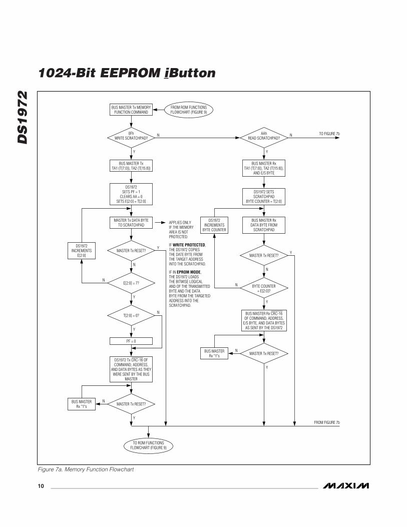
Memory Function CommandsThe Memory Function Flowchart (Figure 7) describesthe protocols necessary for accessing the memory ofthe DS1972. An example on how to use these functionsto write to and read from the device is in the MemoryFunction Example section. The communicationbetween the master and the DS1972 takes place eitherat standard speed (default, OD = 0) or at overdrivespeed (OD = 1). If not explicitly set into overdrivemode, the DS1972 assumes standard speed.
Write Scratchpad [0Fh]The Write Scratchpad command applies to the datamemory and the writable addresses in the registerpage. For the scratchpad data to be valid for copyingto the array, the user must perform a Write Scratchpadcommand of 8 bytes starting at a valid row boundary.The Write Scratchpad command accepts invalidaddresses and partial rows, but subsequent CopyScratchpad commands are blocked.
After issuing the Write Scratchpad command, the mas-ter must first provide the 2-byte target address, fol-lowed by the data to be written to the scratchpad. Thedata is written to the scratchpad starting at the byte off-set of T[2:0]. The E/S bits E[2:0] are loaded with thestarting byte offset and increment with each subse-quent byte. Effectively, E[2:0] is the byte offset of thelast full byte written to the scratchpad. Only full databytes are accepted.
When executing the Write Scratchpad command, theCRC generator inside the DS1972 (Figure 13) calcu-lates a CRC of the entire data stream, starting at thecommand code and ending at the last data byte assent by the master. This CRC is generated using theCRC-16 polynomial by first clearing the CRC generatorand then shifting in the command code (0Fh) of theWrite Scratchpad command, the target addresses (TA1and TA2), and all the data bytes. Note that the CRC-16calculation is performed with the actual TA1 and TA2and data sent by the master. The master can end theWrite Scratchpad command at any time. However, ifthe end of the scratchpad is reached (E[2:0] = 111b),the master can send 16 read time slots and receive theCRC generated by the DS1972.
If a Write Scratchpad command is attempted to a write-protected location, the scratchpad is loaded with thedata already existing in memory rather than the datatransmitted. Similarly, if the target address page is inEPROM mode, the scratchpad is loaded with the bit-wise logical AND of the transmitted data and dataalready existing in memory.
Read Scratchpad [AAh]The Read Scratchpad command allows verifying thetarget address and the integrity of the scratchpad data.After issuing the command code, the master beginsreading. The first 2 bytes are the target address. Thenext byte is the ending offset/data status byte (E/S) fol-lowed by the scratchpad data, which may be differentfrom what the master originally sent. This is of particularimportance if the target address is within the registerpage or a page in either write-protection mode orEPROM mode. See the Write Scratchpad [0Fh] sectionfor details. The master should read through the scratch-pad (E[2:0] - T[2:0] + 1 bytes), after which it receivesthe inverted CRC based on data as it was sent by theDS1972. If the master continues reading after the CRC,all data is logic 1.
DS
19
72
1024-Bit EEPROM iButton
10 ______________________________________________________________________________________
BUS MASTER Tx MEMORYFUNCTION COMMAND
BUS MASTER TxTA1 (T[7:0]), TA2 (T[15:8])
BUS MASTER RxTA1 (T[7:0]), TA2 (T[15:8]),
AND E/S BYTE
BUS MASTER RxDATA BYTE FROM
SCRATCHPAD
MASTER Tx DATA BYTETO SCRATCHPAD APPLIES ONLY
IF THE MEMORYAREA IS NOTPROTECTED.
IF WRITE PROTECTED,THE DS1972 COPIESTHE DATE BYTE FROMTHE TARGET ADDRESSINTO THE SCRATCHPAD.
IF IN EPROM MODE,THE DS1972 LOADSTHE BITWISE LOGICALAND OF THE TRANSMITTEDBYTE AND THE DATABYTE FROM THE TARGETEDADDRESS INTO THESCRATCHPAD.
BUS MASTERRx "1"s
DS1972INCREMENTS
E[2:0]
PF = 0
DS1972SETS PF = 1
CLEARS AA = 0SETS E[2:0] = T[2:0]
0FhWRITE SCRATCHPAD?
N
Y
N
Y
N
Y
Y
Y
N
N
MASTER Tx RESET?
E[2:0] = 7?
T[2:0] = 0?
MASTER Tx RESET?
DS1972 SETSSCRATCHPAD
BYTE COUNTER = T[2:0]
AAhREAD SCRATCHPAD?
N
Y
DS1972 Tx CRC-16 OFCOMMAND, ADDRESS,
AND DATA BYTES AS THEYWERE SENT BY THE BUS
MASTER
BUS MASTERRx "1"s
Y
NMASTER Tx RESET?
BUS MASTER Rx CRC-16OF COMMAND, ADDRESS,
E/S BYTE, AND DATA BYTESAS SENT BY THE DS1972
Y
N
MASTER Tx RESET?
Y
BYTE COUNTER= E[2:0]?
FROM ROM FUNCTIONSFLOWCHART (FIGURE 9)
TO ROM FUNCTIONSFLOWCHART (FIGURE 9)
DS1972INCREMENTS
BYTE COUNTER
N
TO FIGURE 7b
FROM FIGURE 7b
Figure 7a. Memory Function Flowchart

DS
19
72
1024-Bit EEPROM iButton
______________________________________________________________________________________ 11
BUS MASTER TxTA1 (T[7:0]), TA2 (T[15:8])
APPLICABLE TO ALL R/WMEMORY LOCATIONS.
DURATION: tPROG *
* 1-Wire IDLE HIGH FOR POWER.
DS1972 COPIESSCRATCHPAD
DATA TO ADDRESS
BUS MASTERRx "1"s
AA = 1
BUS MASTERRx "1"s
MASTER Tx RESET?N Y
N
N
MASTER Tx RESET?
Y
MASTER Tx RESET?
BUS MASTER TxTA1 (T[7:0]), TA2 (T[15:8])
AND E/S BYTE
55hCOPY SCRATCHPAD?
N
Y
Y
Y
N
DS1972 Tx "0"
DS1972 Tx "1"
F0hREAD MEMORY?
N
Y
Y
N
AUTH. CODEMATCH?
Y
N
Y
N
N
T[15:0] < 0090h?
PF = 0?
ADDRESS < 90h?
YCOPY PROTECTED?
BUS MASTERRx "1"s
MASTER Tx RESET?N
Y
DS1972 SETS MEMORYADDRESS = (T[15:0])
BUS MASTER RxDATA BYTE FROM
MEMORY ADDRESS
Y
N
N
MASTER Tx RESET?
ADDRESS < 8Fh?
N
Y
MASTER Tx RESET?
DS1972INCREMENTS
ADDRESSCOUNTER
Y
TO FIGURE 7a
FROM FIGURE 7a
Figure 7b. Memory Function Flowchart (continued)
DS
19
72
1024-Bit EEPROM iButton
12 ______________________________________________________________________________________
Copy Scratchpad [55h]The Copy Scratchpad command is used to copy datafrom the scratchpad to writable memory sections. Afterissuing the Copy Scratchpad command, the mastermust provide a 3-byte authorization pattern, whichshould have been obtained by an immediately preced-ing Read Scratchpad command. This 3-byte patternmust exactly match the data contained in the threeaddress registers (TA1, TA2, E/S, in that order). If thepattern matches, the target address is valid, the PF flagis not set, and the target memory is not copy protected,then the AA flag is set and the copy begins. All 8 bytesof scratchpad contents are copied to the target memo-ry location. The duration of the device’s internal datatransfer is tPROG during which the voltage on the 1-Wirebus must not fall below 2.8V. A pattern of alternating 0sand 1s are transmitted after the data has been copieduntil the master issues a reset pulse. If the PF flag is setor the target memory is copy protected, the copy doesnot begin and the AA flag is not set.
If the copy command was disturbed due to lack ofpower or for other reasons, the master will read a con-stant stream of FFh bytes until it sends a 1-Wire ResetPulse. In this case, the destination memory may beincompletely programmed requiring a Write Scratchpadcommand and Copy Scratchpad command be repeat-ed to ensure proper programming of the EEPROM. Thisrequires careful consideration when designing applica-tion software that writes to the DS1972 in an intermittentcontact environment.
Read Memory [F0h]The Read Memory command is the general function toread data from the DS1972. After issuing the com-mand, the master must provide the 2-byte targetaddress. After these 2 bytes, the master reads databeginning from the target address and can continueuntil address 008Fh. If the master continues reading,the result is logic 1s. The device’s internal TA1, TA2,E/S, and scratchpad contents are not affected by aRead Memory command.
1-Wire Bus SystemThe 1-Wire bus is a system that has a single bus mas-ter and one or more slaves. In all instances the DS1972is a slave device. The bus master is typically a micro-controller. The discussion of this bus system is broken
down into three topics: hardware configuration, trans-action sequence, and 1-Wire signaling (signal typesand timing). The 1-Wire protocol defines bus transac-tions in terms of the bus state during specific time slots,which are initiated on the falling edge of sync pulsesfrom the bus master.
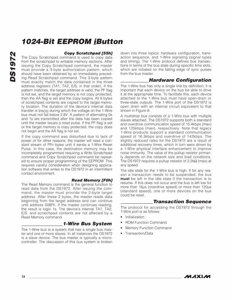
Hardware ConfigurationThe 1-Wire bus has only a single line by definition; it isimportant that each device on the bus be able to driveit at the appropriate time. To facilitate this, each deviceattached to the 1-Wire bus must have open-drain orthree-state outputs. The 1-Wire port of the DS1972 isopen drain with an internal circuit equivalent to thatshown in Figure 8.
A multidrop bus consists of a 1-Wire bus with multipleslaves attached. The DS1972 supports both a standardand overdrive communication speed of 15.4kbps (max)and 125kbps (max), respectively. Note that legacy1-Wire products support a standard communicationspeed of 16.3kbps and overdrive of 142kbps. Theslightly reduced rates for the DS1972 are a result ofadditional recovery times, which in turn were driven bya 1-Wire physical interface enhancement to improvenoise immunity. The value of the pullup resistor primari-ly depends on the network size and load conditions.The DS1972 requires a pullup resistor of 2.2kΩ (max) atany speed.
The idle state for the 1-Wire bus is high. If for any rea-son a transaction needs to be suspended, the busmust be left in the idle state if the transaction is toresume. If this does not occur and the bus is left low formore than 16µs (overdrive speed) or more than 120µs(standard speed), one or more devices on the buscould be reset.
Transaction SequenceThe protocol for accessing the DS1972 through the 1-Wire port is as follows:
• Initialization
• ROM Function Command
• Memory Function Command
• Transaction/Data

DS
19
72
1024-Bit EEPROM iButton
______________________________________________________________________________________ 13
InitializationAll transactions on the 1-Wire bus begin with an initial-ization sequence. The initialization sequence consistsof a reset pulse transmitted by the bus master followedby presence pulse(s) transmitted by the slave(s). Thepresence pulse lets the bus master know that theDS1972 is on the bus and is ready to operate. For moredetails, see the 1-Wire Signaling section.
1-Wire ROM FunctionCommands
Once the bus master has detected a presence, it canissue one of the seven ROM function commands theDS1972 supports. All ROM function commands are 8bits long. A list of these commands follows (see theflowchart in Figure 9).
Read ROM [33h]The Read ROM command allows the bus master to readthe DS1972’s 8-bit family code, unique 48-bit serial num-ber, and 8-bit CRC. This command can only be used ifthere is a single slave on the bus. If more than one slaveis present on the bus, a data collision occurs when allslaves try to transmit at the same time (open drain pro-duces a wired-AND result). The resultant family code and48-bit serial number result in a mismatch of the CRC.
Match ROM [55h]The Match ROM command, followed by a 64-bit ROMsequence, allows the bus master to address a specificDS1972 on a multidrop bus. Only the DS1972 that exact-ly matches the 64-bit ROM sequence responds to thesubsequent memory function command. All other slaveswait for a reset pulse. This command can be used with asingle device or multiple devices on the bus.
Search ROM [F0h]When a system is initially brought up, the bus mastermight not know the number of devices on the 1-Wirebus or their registration numbers. By taking advantageof the wired-AND property of the bus, the master canuse a process of elimination to identify the registrationnumbers of all slave devices. For each bit of the regis-tration number, starting with the least significant bit, thebus master issues a triplet of time slots. On the first slot,each slave device participating in the search outputsthe true value of its registration number bit. On the sec-ond slot, each slave device participating in the searchoutputs the complemented value of its registration num-ber bit. On the third slot, the master writes the truevalue of the bit to be selected. All slave devices that donot match the bit written by the master stop participat-ing in the search. If both of the read bits are zero, themaster knows that slave devices exist with both statesof the bit. By choosing which state to write, the busmaster branches in the ROM code tree. After one com-plete pass, the bus master knows the registration num-ber of a single device. Additional passes identify theregistration numbers of the remaining devices. Refer toApplication Note 187: 1-Wire Search Algorithm for adetailed discussion, including an example.
Skip ROM [CCh]This command can save time in a single-drop bus sys-tem by allowing the bus master to access the memoryfunctions without providing the 64-bit ROM code. Ifmore than one slave is present on the bus and, forexample, a read command is issued following the SkipROM command, data collision occurs on the bus asmultiple slaves transmit simultaneously (open-drainpulldowns produce a wired-AND result).
Rx
RPUP
IL
VPUP
BUS MASTER
OPEN-DRAINPORT PIN 100Ω MOSFET
Tx
Rx
Tx
DATA
DS1972 1-Wire PORT
Rx = RECEIVETx = TRANSMIT
Figure 8. Hardware Configuration

DS
19
72
1024-Bit EEPROM iButton
14 ______________________________________________________________________________________
DS1972 TxPRESENCE PULSE
BUS MASTER TxRESET PULSE
BUS MASTER Tx ROMFUNCTION COMMAND
DS1972 TxCRC BYTE
DS1972 TxFAMILY CODE
(1 BYTE)
DS1972 TxSERIAL NUMBER
(6 BYTES)
RC = 0
MASTER Tx BIT 0
RC = 0 RC = 0 RC = 0
OD = 0
YY
Y
Y
Y
Y
Y
Y
33hREAD ROM
COMMAND?N
55hMATCH ROMCOMMAND?
BIT 0 MATCH? BIT 0 MATCH?
N
N N
N N
N N
F0hSEARCH ROMCOMMAND?
ODRESET PULSE?
N
N
CChSKIP ROM
COMMAND?N
RC = 1
MASTER Tx BIT 1
MASTER Tx BIT 63
BIT 1 MATCH?
BIT 63 MATCH?
Y
Y
RC = 1
FROM MEMORY FUNCTIONSFLOWCHART (FIGURE 7)
TO MEMORY FUNCTIONSFLOWCHART (FIGURE 7)
DS1972 Tx BIT 0
DS1972 Tx BIT 0
MASTER Tx BIT 0
BIT 1 MATCH?
BIT 63 MATCH?
DS1972 Tx BIT 1
DS1972 Tx BIT 1
MASTER Tx BIT 1
DS1972 Tx BIT 63
DS1972 Tx BIT 63
MASTER Tx BIT 63
Y
TO FIGURE 9b
TO FIGURE 9b
FROM FIGURE 9b
FROM FIGURE 9b
Figure 9a. ROM Functions Flowchart

DS
19
72
1024-Bit EEPROM iButton
______________________________________________________________________________________ 15
RC = 0; OD = 1 RC = 0; OD = 1
N
BIT 0 MATCH?
YN
RC = 1?
Y
A5hRESUME
COMMAND?N
Y
3ChOVERDRIVE-SKIP ROM?
N
Y
69hOVERDRIVE-
MATCH ROM?
FROM FIGURE 9a
FROM FIGURE 9a
TO FIGURE 9a
NOTE: THE OD FLAG REMAINS AT 1 IF THE DEVICE WAS ALREADY AT OVERDRIVE SPEED BEFORE THE OVERDRIVE-MATCH ROM COMMAND WAS ISSUED.
TO FIGURE 9a
N
Y
Y
N
MASTER TxRESET?
YMASTER TxRESET?
N BIT 1 MATCH?
MASTER Tx BIT 0
MASTER Tx BIT 1
OD = 0
(SEE NOTE)
(SEE NOTE)
(SEE NOTE)
NOD = 0
NOD = 0
Y
RC = 1
BIT 63 MATCH?
MASTER Tx BIT 63
Y
Figure 9b. ROM Functions Flowchart (continued)

DS
19
72
1024-Bit EEPROM iButton
16 ______________________________________________________________________________________
Resume [A5h]To maximize the data throughput in a multidrop envi-ronment, the Resume command is available. This com-mand checks the status of the RC bit and, if it is set,directly transfers control to the memory function com-mands, similar to a Skip ROM command. The only wayto set the RC bit is through successfully executing theMatch ROM, Search ROM, or Overdrive-Match ROMcommand. Once the RC bit is set, the device canrepeatedly be accessed through the Resume com-mand. Accessing another device on the bus clears theRC bit, preventing two or more devices from simultane-ously responding to the Resume command.
Overdrive-Skip ROM [3Ch]On a single-drop bus this command can save time byallowing the bus master to access the memory func-tions without providing the 64-bit ROM code. Unlike thenormal Skip ROM command, the Overdrive-Skip ROMcommand sets the DS1972 into the overdrive mode(OD = 1). All communication following this commandmust occur at overdrive speed until a reset pulse ofminimum 480µs duration resets all devices on the busto standard speed (OD = 0).
When issued on a multidrop bus, this command sets alloverdrive-supporting devices into overdrive mode. Tosubsequently address a specific overdrive-supportingdevice, a reset pulse at overdrive speed must beissued followed by a Match ROM or Search ROM com-mand sequence. This speeds up the time for thesearch process. If more than one slave supportingoverdrive is present on the bus and the Overdrive-SkipROM command is followed by a read command, datacollision occurs on the bus as multiple slaves transmitsimultaneously (open-drain pulldowns produce a wired-AND result).
Overdrive-Match ROM [69h]The Overdrive-Match ROM command followed by a 64-bit ROM sequence transmitted at overdrive speedallows the bus master to address a specific DS1972 ona multidrop bus and to simultaneously set it in overdrivemode. Only the DS1972 that exactly matches the 64-bitROM sequence responds to the subsequent memoryfunction command. Slaves already in overdrive modefrom a previous Overdrive-Skip ROM or successfulOverdrive-Match ROM command remain in overdrivemode. All overdrive-capable slaves return to standardspeed at the next reset pulse of minimum 480µs dura-tion. The Overdrive-Match ROM command can be usedwith a single device or multiple devices on the bus.
1-Wire SignalingThe DS1972 requires strict protocols to ensure dataintegrity. The protocol consists of four types of signal-ing on one line: reset sequence with reset pulse andpresence pulse, write-zero, write-one, and read-data.Except for the presence pulse, the bus master initiatesall falling edges. The DS1972 can communicate at twodifferent speeds: standard speed and overdrive speed.If not explicitly set into the overdrive mode, the DS1972communicates at standard speed. While in overdrivemode, the fast timing applies to all waveforms.
To get from idle to active, the voltage on the 1-Wire lineneeds to fall from VPUP below the threshold VTL. To getfrom active to idle, the voltage needs to rise from VILMAX past the threshold VTH. The time it takes for thevoltage to make this rise is seen in Figure 10 as ε, andits duration depends on the pullup resistor (RPUP) usedand the capacitance of the 1-Wire network attached.The voltage VILMAX is relevant for the DS1972 whendetermining a logical level, not triggering any events.
Figure 10 shows the initialization sequence required tobegin any communication with the DS1972. A resetpulse followed by a presence pulse indicates that theDS1972 is ready to receive data, given the correctROM and memory function command. If the bus masteruses slew-rate control on the falling edge, it must pulldown the line for tRSTL + tF to compensate for theedge. A tRSTL duration of 480µs or longer exits theoverdrive mode, returning the device to standardspeed. If the DS1972 is in overdrive mode and tRSTL isno longer than 80µs, the device remains in overdrivemode. If the device is in overdrive mode and tRSTL isbetween 80µs and 480µs, the device resets, but thecommunication speed is undetermined.
After the bus master has released the line it goes intoreceive mode. Now the 1-Wire bus is pulled to VPUPthrough the pullup resistor or, in the case of a DS2482-x00 or DS2480B driver, through the active circuitry.When the threshold VTH is crossed, the DS1972 waitsfor tPDH and then transmits a presence pulse by pullingthe line low for tPDL. To detect a presence pulse, themaster must test the logical state of the 1-Wire line attMSP.
The tRSTH window must be at least the sum oftPDHMAX, tPDLMAX, and tRECMIN. Immediately aftertRSTH is expired, the DS1972 is ready for data commu-nication. In a mixed population network, tRSTH shouldbe extended to minimum 480µs at standard speed and48µs at overdrive speed to accommodate other 1-Wiredevices.

DS
19
72
1024-Bit EEPROM iButton
______________________________________________________________________________________ 17
Read/Write Time SlotsData communication with the DS1972 takes place intime slots that carry a single bit each. Write time slotstransport data from bus master to slave. Read timeslots transfer data from slave to master. Figure 11 illus-trates the definitions of the write and read time slots.
All communication begins with the master pulling thedata line low. As the voltage on the 1-Wire line fallsbelow the threshold VTL, the DS1972 starts its internaltiming generator that determines when the data line issampled during a write time slot and how long data isvalid during a read time slot.
Master-to-SlaveFor a write-one time slot, the voltage on the data linemust have crossed the VTH threshold before the write-one low time tW1LMAX is expired. For a write-zero timeslot, the voltage on the data line must stay below theVTH threshold until the write-zero low time tW0LMIN isexpired. For the most reliable communication, the volt-age on the data line should not exceed VILMAX duringthe entire tW0L or tW1L window. After the VTH thresholdhas been crossed, the DS1972 needs a recovery timetREC before it is ready for the next time slot.
Slave-to-MasterA read-data time slot begins like a write-one time slot.The voltage on the data line must remain below VTLuntil the read low time tRL is expired. During the tRLwindow, when responding with a 0, the DS1972 startspulling the data line low; its internal timing generatordetermines when this pulldown ends and the voltagestarts rising again. When responding with a 1, theDS1972 does not hold the data line low at all, and thevoltage starts rising as soon as tRL is over.
The sum of tRL + δ (rise time) on one side and the inter-nal timing generator of the DS1972 on the other sidedefine the master sampling window (tMSRMIN totMSRMAX), in which the master must perform a readfrom the data line. For the most reliable communication,tRL should be as short as permissible, and the mastershould read close to but no later than tMSRMAX. Afterreading from the data line, the master must wait untiltSLOT is expired. This guarantees sufficient recoverytime tREC for the DS1972 to get ready for the next timeslot. Note that tREC specified herein applies only to asingle DS1972 attached to a 1-Wire line. For multide-vice configurations, tREC must be extended to accom-modate the additional 1-Wire device input capacitance.Alternatively, an interface that performs active pullupduring the 1-Wire recovery time such as the DS2482-x00 or DS2480B 1-Wire line drivers can be used.
RESISTOR MASTER DS1972
tRSTL tPDL
tRSTH
tPDH
MASTER Tx "RESET PULSE" MASTER Rx "PRESENCE PULSE"
VPUPVIHMASTER
VTH
VTLVILMAX
0V
ε
tF
tREC
tMSP
Figure 10. Initialization Procedure: Reset and Presence Pulse

DS
19
72
1024-Bit EEPROM iButton
18 ______________________________________________________________________________________
RESISTOR MASTER
RESISTOR MASTER
RESISTOR MASTER DS1972
ε
ε
δ
VPUPVIHMASTER
VTH
VTLVILMAX
0VtF
VPUPVIHMASTER
VTH
VTLVILMAX
0V
tF
VPUPVIHMASTER
VTH
VTLVILMAX
0VtF
tSLOT
tW1L
tRECtSLOT
tSLOT
tW0L
tREC
MASTERSAMPLINGWINDOW
tRL
tMSR
WRITE-ONE TIME SLOT
WRITE-ZERO TIME SLOT
READ-DATA TIME SLOT
Figure 11. Read/Write Timing Diagrams

DS
19
72
1024-Bit EEPROM iButton
______________________________________________________________________________________ 19
Improved Network Behavior(Switchpoint Hysteresis)
In a 1-Wire environment, line termination is possibleonly during transients controlled by the bus master (1-Wire driver). 1-Wire networks, therefore, are suscep-tible to noise of various origins. Depending on thephysical size and topology of the network, reflectionsfrom end points and branch points can add up or can-cel each other to some extent. Such reflections are visi-ble as glitches or ringing on the 1-Wire communicationline. Noise coupled onto the 1-Wire line from externalsources can also result in signal glitching. A glitch dur-ing the rising edge of a time slot can cause a slavedevice to lose synchronization with the master and,consequently, result in a Search ROM command com-ing to a dead end or cause a device-specific functioncommand to abort. For better performance in networkapplications, the DS1972 uses a new 1-Wire front-end,which makes it less sensitive to noise.
The DS1972’s 1-Wire front-end differs from traditionalslave devices in three characteristics.
1) There is additional lowpass filtering in the circuit thatdetects the falling edge at the beginning of a timeslot. This reduces the sensitivity to high-frequencynoise. This additional filtering does not apply atoverdrive speed.
2) There is a hysteresis at the low-to-high switchingthreshold VTH. If a negative glitch crosses VTH butdoes not go below VTH - VHY, it is not recognized(Figure 12, Case A). The hysteresis is effective atany 1-Wire speed.
3) There is a time window specified by the rising edgehold-off time tREH during which glitches are ignored,even if they extend below the VTH - VHY threshold
(Figure 12, Case B, tGL < tREH). Deep voltage dropsor glitches that appear late after crossing the VTHthreshold and extend beyond the tREH window can-not be filtered out and are taken as the beginning of anew time slot (Figure 12, Case C, tGL ≥ tREH).
Devices that have the parameters VHY and tREH speci-fied in their electrical characteristics use the improved1-Wire front-end.
CRC GenerationThe DS1972 uses two different types of CRCs. OneCRC is an 8-bit type and is stored in the most signifi-cant byte of the 64-bit ROM. The bus master can com-pute a CRC value from the first 56 bits of the 64-bitROM and compare it to the value stored within theDS1972 to determine if the ROM data has beenreceived error-free. The equivalent polynomial functionof this CRC is X8 + X5 + X4 + 1. This 8-bit CRC isreceived in the true (noninverted) form. It is computedat the factory and lasered into the ROM.
The other CRC is a 16-bit type, generated according tothe standardized CRC-16 polynomial function X16 + X15
+ X2 + 1. This CRC is used for fast verification of a datatransfer when writing to or reading from the scratchpad.In contrast to the 8-bit CRC, the 16-bit CRC is alwayscommunicated in the inverted form. A CRC generatorinside the DS1972 iButton (Figure 13) calculates a new16-bit CRC, as shown in the command flowchart(Figure 7). The bus master compares the CRC valueread from the device to the one it calculates from thedata and decides whether to continue with an operationor to reread the portion of the data with the CRC error.
With the Write Scratchpad command, the CRC is gen-erated by first clearing the CRC generator and thenshifting in the command code, the target addressesTA1 and TA2, and all the data bytes as they were sent
VPUP
VTHVHY
0V
tREH
tGL
tREH
tGL
CASE A CASE CCASE B
Figure 12. Noise Suppression Scheme

DS
19
72
1024-Bit EEPROM iButton
20 ______________________________________________________________________________________
by the bus master. The DS1972 transmits this CRC onlyif E[2:0] = 111b.
With the Read Scratchpad command, the CRC is gen-erated by first clearing the CRC generator and thenshifting in the command code, the target addresses
TA1 and TA2, the E/S byte, and the scratchpad data asthey were sent by the DS1972. The DS1972 transmitsthis CRC only if the reading continues through the endof the scratchpad. For more information on generatingCRC values, refer to Application Note 27.
1STSTAGE
2NDSTAGE
3RDSTAGE
4THSTAGE
7THSTAGE
8THSTAGE
6THSTAGE
5THSTAGE
X0 X1 X2 X3 X4
POLYNOMIAL = X16 + X15 + X2 + 1
INPUT DATA
CRC OUTPUT
X5 X6
11THSTAGE
12THSTAGE
15THSTAGE
14THSTAGE
13THSTAGE
X11 X12
9THSTAGE
10THSTAGE
X9 X10 X13 X14
X7
16THSTAGE
X16X15X8
Figure 13. CRC-16 Hardware Description and Polynomial
Command-Specific 1-Wire Communication Protocol—Legend
SYMBOL DESCRIPTION
RST 1-Wire reset pulse generated by master.
PD 1-Wire presence pulse generated by slave.
Select Command and data to satisfy the ROM function protocol.
WS Command “Write Scratchpad.”
RS Command “Read Scratchpad.”
CPS Command “Copy Scratchpad.”
RM Command “Read Memory.”
TA Target address TA1, TA2.
TA-E/S Target address TA1, TA2 with E/S byte.
<8–T[2:0] bytes> Transfer of as many bytes as needed to reach the end of the scratchpad for a given target address.
<Data to EOM> Transfer of as many data bytes as are needed to reach the end of the memory.
CRC-16 Transfer of an inverted CRC-16.
FF Loop Indefinite loop where the master reads FF bytes.
AA Loop Indefinite loop where the master reads AA bytes.
Programming Data transfer to EEPROM; no activity on the 1-Wire bus permitted during this time.

DS
19
72
1024-Bit EEPROM iButton
______________________________________________________________________________________ 21
Command-Specific 1-Wire Communication Protocol—Color Codes
1-Wire Communication Examples
Master to Slave Slave to Master Programming
Write Scratchpad (Cannot Fail) RST PD Select WS TA <8–T[2:0] bytes> CRC-16 FF Loop
Read Scratchpad (Cannot Fail) RST PD Select RS TA-E/S <8–T[2:0] bytes> CRC-16 FF Loop
Copy Scratchpad (Success) RST PD Select CPS TA-E/S Programming AA Loop
Copy Scratchpad (Invalid Address or PF = 1 or Copy Protected) RST PD Select CPS TA-E/S FF Loop
Read Memory (Success) RST PD Select RM TA <Data to EOM> FF Loop
Read Memory (Invalid Address) RST PD Select RM TA FF Loop

DS
19
72
1024-Bit EEPROM iButton
22 ______________________________________________________________________________________
Memory Function ExampleWrite to the first 8 bytes of memory page 1. Read theentire memory.
With only a single DS1972 connected to the bus mas-ter, the communication looks like this:
MASTER MODE DATA (LSB FIRST) COMMENTS Tx (Reset) Reset pulse Rx (Presence) Presence pulse Tx CCh Issue “Skip ROM” command Tx 0Fh Issue “Write Scratchpad” command Tx 20h TA1, beginning offset = 20h Tx 00h TA2, address = 0020h Tx <8 Data Bytes> Write 8 bytes of data to scratchpad Rx <2 Bytes CRC-16> Read CRC to check for data integrity Tx (Reset) Reset pulse Rx (Presence) Presence pulse Tx CCh Issue “Skip ROM” command Tx AAh Issue “Read Scratchpad” command Rx 20h Read TA1, beginning offset = 20h Rx 00h Read TA2, address = 0020h Rx 07h Read E/S, ending offset = 111b, AA, PF = 0 Rx <8 Data Bytes> Read scratchpad data and verify Rx <2 Bytes CRC-16> Read CRC to check for data integrity Tx (Reset) Reset pulse Rx (Presence) Presence pulse Tx CCh Issue “Skip ROM” command Tx 55h Issue “Copy Scratchpad” command Tx 20h TA1 Tx 00h TA2 Tx 07h E/S
(AUTHORIZATION CODE)
— <1-Wire Idle High> Wait tPROGMAX for the copy function to complete Rx AAh Read copy status, AAh = success Tx (Reset) Reset pulse Rx (Presence) Presence pulse Tx CCh Issue “Skip ROM” command Tx F0h Issue “Read Memory” command Tx 00h TA1, beginning offset = 00h Tx 00h TA2, address = 0000h Rx <144 Data Bytes> Read the entire memory Tx (Reset) Reset pulse Rx (Presence) Presence pulse
PACKAGE TYPE PACKAGE CODE DOCUMENT NO.
F3 iButton IB+3NT 21-0252
F5 iButton IB+5NT 21-0266
Package InformationFor the latest package outline information and land patterns, go to www.maxim-ic.com/packages. Note that a “+”, “#”, or “-” in thepackage code indicates RoHS status only. Package drawings may show a different suffix character, but the drawing pertains to thepackage regardless of RoHS status.

DS
19
72
1024-Bit EEPROM iButton
Maxim cannot assume responsibility for use of any circuitry other than circuitry entirely embodied in a Maxim product. No circuit patent licenses areimplied. Maxim reserves the right to change the circuitry and specifications without notice at any time.
Maxim Integrated Products, 120 San Gabriel Drive, Sunnyvale, CA 94086 408-737-7600 ____________________ 23
© 2012 Maxim Integrated Products Maxim is a registered trademark of Maxim Integrated Products, Inc.
Revision HistoryREVISION NUMBER
REVISION DATE
DESCRIPTION PAGES
CHANGED
0 4/06 Initial release —
1 8/06 UL#913 bullet changed from “Meets UL#93 (4th Edit.). . .(Application Pending)” to “Designed to meet UL#93 (4th Edit.). . .”
1, 2
Deleted UL#913 bullet from the Common iButton Features section. 1
2 8/09 Changed the RoHS packages to lead(Pb)-free packages in the Ordering Informationtable.
1
Changed VTLMIN from 0.46V to 0.5V in the Electrical Characteristics table. 2
In the Absolute Maximum Ratings, changed storage temp to -55°C to +125°C; in the Electrical Characteristics table, changed VTH, VTL based on VPUP and data retention to 40 years min at 85°C; added note to retention spec: “EEPROM writes can become nonfunctional after the data-retention time is exceeded. Long-term storage at elevated temperatures is not recommended; the device can lose its write capability after 10 years at +125°C or 40 years at +85°C.”
2, 3
In the Electrical Characteristics table, changed the VILMAX spec from 0.3V to 0.5V; removed from the tW1LMAX spec; added Note 17 to tW0L spec; updated EC table Notes 17 and 18; corrected Note 20.
2, 3
Added to Figure 11 Write-Zero Time Slot. 18
Added Package Information table. 22
3 4/10
Created newer template-style data sheet. All
4 1/12 Updated Note 1 in the Electrical Characteristics section; specified the data memory default status and added a note that the memory must be programmed to FFh for the EPROM mode to function to the Memory Access section.
3, 7, 8