10 MHz to 3 GHz VGA with 60 dB Gain Control Range Data ... · 60 dB Gain Control Range Data Sheet...
24
10 MHz to 3 GHz VGA with 60 dB Gain Control Range Data Sheet ADL5330 Rev. B Document Feedback Information furnished by Analog Devices is believed to be accurate and reliable. However, no responsibility is assumed by Analog Devices for its use, nor for any infringements of patents or other rights of third parties that may result from its use. Specifications subject to change without notice. No license is granted by implication or otherwise under any patent or patent rights of Analog Devices. Trademarks and registered trademarks are the property of their respective owners. One Technology Way, P.O. Box 9106, Norwood, MA 02062-9106, U.S.A. Tel: 781.329.4700 ©2005–2017 Analog Devices, Inc. All rights reserved. Technical Support www.analog.com FEATURES Voltage controlled amplifier/attenuator Operating frequency 10 MHz to 3 GHz Optimized for controlling output power High linearity: OIP3 31 dBm at 900 MHz Output noise floor: −150 dBm/Hz at 900 MHz 50 Ω input and output impedances Single-ended or differential operation Wide gain control range: −34 dB to +22 dB at 900 MHz Linear in dB gain control function, 20 mV/dB Single-supply 4.75 V to 5.25 V APPLICATIONS Transmit and receive power control at RF and IF FUNCTIONAL BLOCK DIAGRAM INLO VPS1 COM1 INHI COM2 OPLO OPHI IPBS GAIN CONTROL BIAS AND VREF GAIN BALUN COM2 RFOUT COM2 VPS2 VPS2 VPS2 COM1 VPS1 VPS2 VPS2 COM2 COM1 OPBS VREF ENBL VPS2 RFIN 05134-001 INPUT GM STAGE O/P (TZ) STAGE CONTINUOUSLY VARIABLE ATTENUATOR Figure 1. GENERAL DESCRIPTION The ADL5330 is a high performance, voltage controlled, variable gain amplifier (VGA)/attenuator for use in applications with frequencies up to 3 GHz. The balanced structure of the signal path minimizes distortion while it also reduces the risk of spurious feedforward at low gains and high frequencies caused by parasitic coupling. While operation between a balanced source and load is recommended, a single sided input is internally converted to differential form. The input impedance is 50 Ω from INHI to INLO. The outputs are usually coupled into a 50 Ω grounded load via a 1:1 balun. A single supply of 4.75 V to 5.25 V is required. The 50 Ω input system converts the applied voltage to a pair of differential currents with high linearity and good common rejection even when driven by a single sided source. The signal currents are then applied to a proprietary voltage controlled attenuator providing precise definition of the overall gain under the control of the linear in dB interface. The GAIN pin accepts a voltage from 0 V at minimum gain to 1.4 V at full gain with a 20 mV/dB scaling factor. The output of the high accuracy wideband attenuator is applied to a differential transimpedance output stage. The output stage sets the 50 Ω differential output impedances and drives the OPHI and OPLO pins. The ADL5330 has a power-down function. It can be powered down by a Logic LO input on the ENBL pin. The current consumption in power-down mode is 250 μA. The ADL5330 is fabricated on an Analog Devices, Inc., proprietary high performance, complementary bipolar IC process. The ADL5330 is available in a 24-lead (4 mm × 4 mm), Pb-free LFCSP package and is specified for operation from ambient temperatures of −40°C to +85°C. An evaluation board is also available.
Transcript of 10 MHz to 3 GHz VGA with 60 dB Gain Control Range Data ... · 60 dB Gain Control Range Data Sheet...

10 MHz to 3 GHz VGA with60 dB Gain Control Range
Data Sheet ADL5330
Rev. B Document Feedback Information furnished by Analog Devices is believed to be accurate and reliable. However, no responsibility is assumed by Analog Devices for its use, nor for any infringements of patents or other rights of third parties that may result from its use. Specifications subject to change without notice. No license is granted by implication or otherwise under any patent or patent rights of Analog Devices. Trademarks and registered trademarks are the property of their respective owners.
One Technology Way, P.O. Box 9106, Norwood, MA 02062-9106, U.S.A.Tel: 781.329.4700 ©2005–2017 Analog Devices, Inc. All rights reserved. Technical Support www.analog.com
FEATURES Voltage controlled amplifier/attenuator Operating frequency 10 MHz to 3 GHz Optimized for controlling output power High linearity: OIP3 31 dBm at 900 MHz Output noise floor: −150 dBm/Hz at 900 MHz 50 Ω input and output impedances Single-ended or differential operation Wide gain control range: −34 dB to +22 dB at 900 MHz Linear in dB gain control function, 20 mV/dB Single-supply 4.75 V to 5.25 V
APPLICATIONS Transmit and receive power control at RF and IF
FUNCTIONAL BLOCK DIAGRAM
INLO
VPS1
COM1
INHI
COM2
OPLO
OPHI
IPBS
GAINCONTROL
BIASANDVREF
GAIN
BALUN
COM2
RFOUT
COM2
VPS2
VPS2
VPS2
COM1
VPS1
VPS2VPS2
COM2COM1OPBSVREF
ENBL VPS2
RFIN
05134-0
01
INPUTGM
STAGE
O/P(TZ)
STAGE
CO
NT
INU
OU
SL
YV
AR
IAB
LE
AT
TE
NU
AT
OR
Figure 1.
GENERAL DESCRIPTION The ADL5330 is a high performance, voltage controlled, variable gain amplifier (VGA)/attenuator for use in applications with frequencies up to 3 GHz. The balanced structure of the signal path minimizes distortion while it also reduces the risk of spurious feedforward at low gains and high frequencies caused by parasitic coupling. While operation between a balanced source and load is recommended, a single sided input is internally converted to differential form.
The input impedance is 50 Ω from INHI to INLO. The outputs are usually coupled into a 50 Ω grounded load via a 1:1 balun. A single supply of 4.75 V to 5.25 V is required.
The 50 Ω input system converts the applied voltage to a pair of differential currents with high linearity and good common rejection even when driven by a single sided source. The signal currents are then applied to a proprietary voltage controlled attenuator providing precise definition of the overall gain under the control of the linear in dB interface. The GAIN pin accepts a voltage from 0 V at minimum gain to 1.4 V at full gain with a 20 mV/dB scaling factor.
The output of the high accuracy wideband attenuator is applied to a differential transimpedance output stage. The output stage sets the 50 Ω differential output impedances and drives the OPHI and OPLO pins. The ADL5330 has a power-down function. It can be powered down by a Logic LO input on the ENBL pin. The current consumption in power-down mode is 250 μA.
The ADL5330 is fabricated on an Analog Devices, Inc., proprietary high performance, complementary bipolar IC process. The ADL5330 is available in a 24-lead (4 mm × 4 mm), Pb-free LFCSP package and is specified for operation from ambient temperatures of −40°C to +85°C. An evaluation board is also available.
ADL5330 Data Sheet
Rev. B | Page 2 of 24
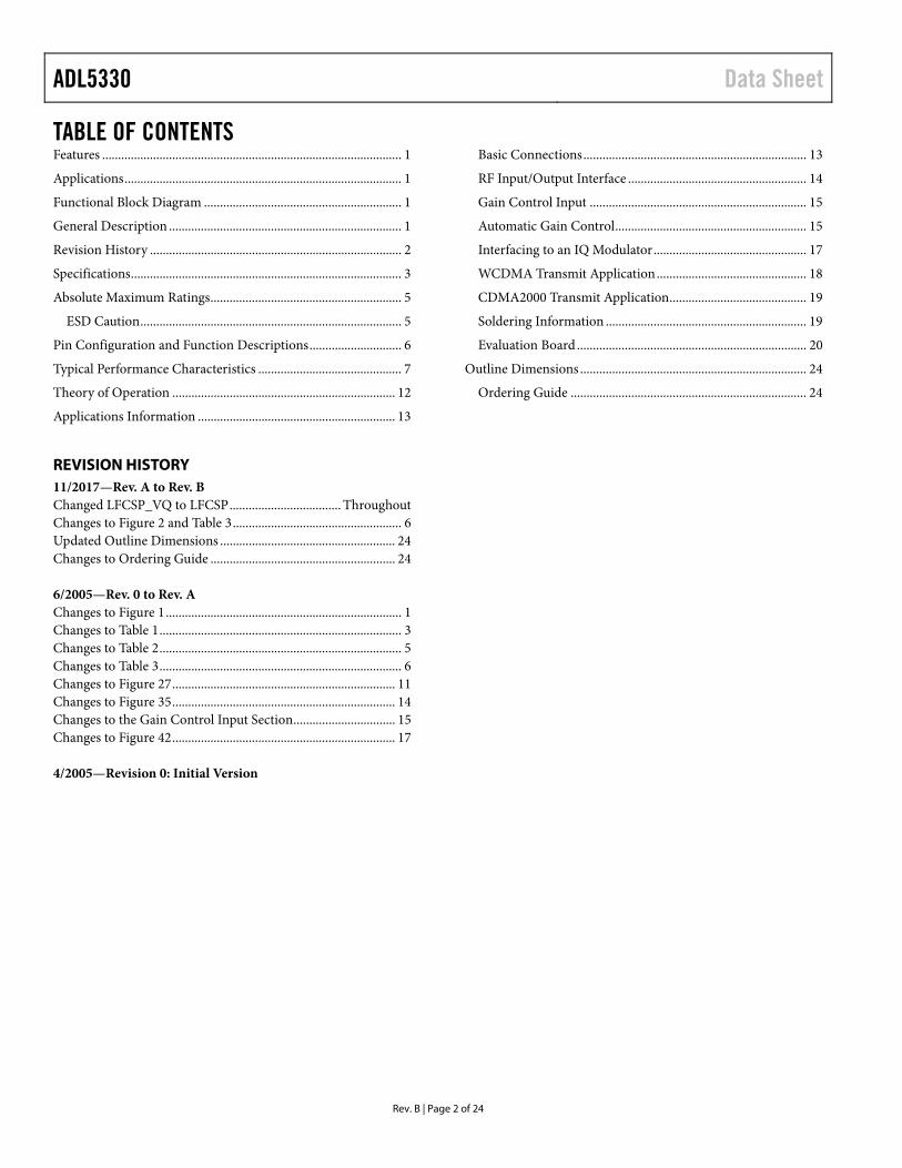
TABLE OF CONTENTS Features .............................................................................................. 1
Applications ....................................................................................... 1
Functional Block Diagram .............................................................. 1
General Description ......................................................................... 1
Revision History ............................................................................... 2
Specifications ..................................................................................... 3
Absolute Maximum Ratings ............................................................ 5
ESD Caution .................................................................................. 5
Pin Configuration and Function Descriptions ............................. 6
Typical Performance Characteristics ............................................. 7
Theory of Operation ...................................................................... 12
Applications Information .............................................................. 13
Basic Connections ...................................................................... 13
RF Input/Output Interface ........................................................ 14
Gain Control Input .................................................................... 15
Automatic Gain Control ............................................................ 15
Interfacing to an IQ Modulator ................................................ 17
WCDMA Transmit Application ............................................... 18
CDMA2000 Transmit Application ........................................... 19
Soldering Information ............................................................... 19
Evaluation Board ........................................................................ 20
Outline Dimensions ....................................................................... 24
Ordering Guide .......................................................................... 24
REVISION HISTORY 11/2017—Rev. A to Rev. B Changed LFCSP_VQ to LFCSP ................................... Throughout Changes to Figure 2 and Table 3 ..................................................... 6 Updated Outline Dimensions ....................................................... 24 Changes to Ordering Guide .......................................................... 24 6/2005—Rev. 0 to Rev. A Changes to Figure 1 .......................................................................... 1 Changes to Table 1 ............................................................................ 3 Changes to Table 2 ............................................................................ 5 Changes to Table 3 ............................................................................ 6 Changes to Figure 27 ...................................................................... 11 Changes to Figure 35 ...................................................................... 14 Changes to the Gain Control Input Section ................................ 15 Changes to Figure 42 ...................................................................... 17 4/2005—Revision 0: Initial Version
Data Sheet ADL5330
Rev. B | Page 3 of 24
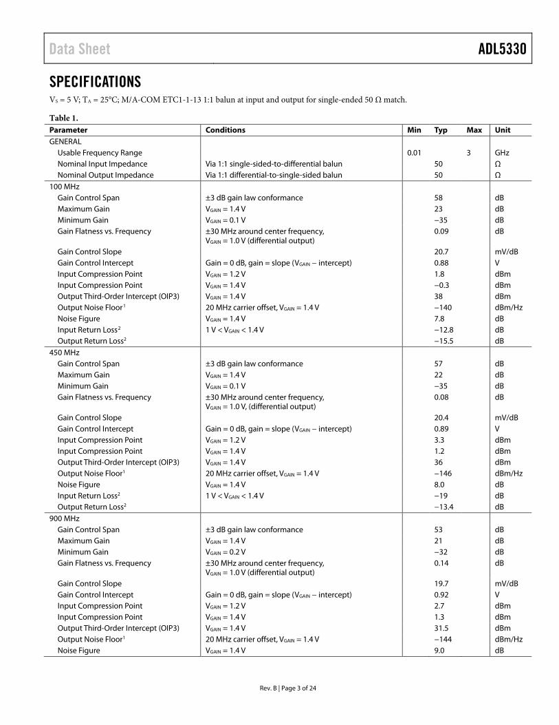
SPECIFICATIONS VS = 5 V; TA = 25°C; M/A-COM ETC1-1-13 1:1 balun at input and output for single-ended 50 Ω match.
Table 1. Parameter Conditions Min Typ Max Unit GENERAL
Usable Frequency Range 0.01 3 GHz Nominal Input Impedance Via 1:1 single-sided-to-differential balun 50 Ω Nominal Output Impedance Via 1:1 differential-to-single-sided balun 50 Ω
100 MHz Gain Control Span ±3 dB gain law conformance 58 dB Maximum Gain VGAIN = 1.4 V 23 dB Minimum Gain VGAIN = 0.1 V −35 dB Gain Flatness vs. Frequency ±30 MHz around center frequency,
VGAIN = 1.0 V (differential output) 0.09 dB
Gain Control Slope 20.7 mV/dB Gain Control Intercept Gain = 0 dB, gain = slope (VGAIN − intercept) 0.88 V Input Compression Point VGAIN = 1.2 V 1.8 dBm Input Compression Point VGAIN = 1.4 V −0.3 dBm Output Third-Order Intercept (OIP3) VGAIN = 1.4 V 38 dBm Output Noise Floor1 20 MHz carrier offset, VGAIN = 1.4 V −140 dBm/Hz Noise Figure VGAIN = 1.4 V 7.8 dB Input Return Loss2 1 V < VGAIN < 1.4 V −12.8 dB Output Return Loss2 −15.5 dB
450 MHz Gain Control Span ±3 dB gain law conformance 57 dB Maximum Gain VGAIN = 1.4 V 22 dB Minimum Gain VGAIN = 0.1 V −35 dB Gain Flatness vs. Frequency ±30 MHz around center frequency,
VGAIN = 1.0 V, (differential output) 0.08 dB
Gain Control Slope 20.4 mV/dB Gain Control Intercept Gain = 0 dB, gain = slope (VGAIN − intercept) 0.89 V Input Compression Point VGAIN = 1.2 V 3.3 dBm Input Compression Point VGAIN = 1.4 V 1.2 dBm Output Third-Order Intercept (OIP3) VGAIN = 1.4 V 36 dBm Output Noise Floor1 20 MHz carrier offset, VGAIN = 1.4 V −146 dBm/Hz Noise Figure VGAIN = 1.4 V 8.0 dB Input Return Loss2 1 V < VGAIN < 1.4 V −19 dB Output Return Loss2 −13.4 dB
900 MHz Gain Control Span ±3 dB gain law conformance 53 dB Maximum Gain VGAIN = 1.4 V 21 dB Minimum Gain VGAIN = 0.2 V −32 dB Gain Flatness vs. Frequency ±30 MHz around center frequency,
VGAIN = 1.0 V (differential output) 0.14 dB
Gain Control Slope 19.7 mV/dB Gain Control Intercept Gain = 0 dB, gain = slope (VGAIN − intercept) 0.92 V Input Compression Point VGAIN = 1.2 V 2.7 dBm Input Compression Point VGAIN = 1.4 V 1.3 dBm Output Third-Order Intercept (OIP3) VGAIN = 1.4 V 31.5 dBm Output Noise Floor1 20 MHz carrier offset, VGAIN = 1.4 V −144 dBm/Hz Noise Figure VGAIN = 1.4 V 9.0 dB
ADL5330 Data Sheet
Rev. B | Page 4 of 24
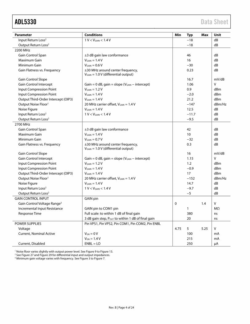
Parameter Conditions Min Typ Max Unit Input Return Loss2 1 V < VGAIN < 1.4 V −18 dB Output Return Loss2 −18 dB
2200 MHz Gain Control Span ±3 dB gain law conformance 46 dB Maximum Gain VGAIN = 1.4 V 16 dB Minimum Gain VGAIN = 0.6 V −30 dB Gain Flatness vs. Frequency ±30 MHz around center frequency,
VGAIN = 1.0 V (differential output) 0.23 dB
Gain Control Slope 16.7 mV/dB Gain Control Intercept Gain = 0 dB, gain = slope (VGAIN − intercept) 1.06 V Input Compression Point VGAIN = 1.2 V 0.9 dBm Input Compression Point VGAIN = 1.4 V −2.0 dBm Output Third-Order Intercept (OIP3) VGAIN = 1.4 V 21.2 dBm Output Noise Floor1 20 MHz carrier offset, VGAIN = 1.4 V −147 dBm/Hz Noise Figure VGAIN = 1.4 V 12.5 dB Input Return Loss2 1 V < VGAIN < 1.4 V −11.7 dB Output Return Loss2 −9.5 dB
2700 MHz Gain Control Span ±3 dB gain law conformance 42 dB Maximum Gain VGAIN = 1.4 V 10 dB Minimum Gain VGAIN = 0.7 V −32 dB Gain Flatness vs. Frequency ±30 MHz around center frequency,
VGAIN = 1.0 V (differential output) 0.3 dB
Gain Control Slope 16 mV/dB Gain Control Intercept Gain = 0 dB, gain = slope (VGAIN − intercept) 1.15 V Input Compression Point VGAIN = 1.2 V 1.2 dBm Input Compression Point VGAIN = 1.4 V −0.9 dBm Output Third-Order Intercept (OIP3) VGAIN = 1.4 V 17 dBm Output Noise Floor1 20 MHz carrier offset, VGAIN = 1.4 V −152 dBm/Hz Noise Figure VGAIN = 1.4 V 14.7 dB Input Return Loss2 1 V < VGAIN < 1.4 V −9.7 dB Output Return Loss2 −5 dB
GAIN CONTROL INPUT GAIN pin Gain Control Voltage Range3 0 1.4 V Incremental Input Resistance GAIN pin to COM1 pin 1 MΩ Response Time Full scale: to within 1 dB of final gain 380 ns 3 dB gain step, POUT to within 1 dB of final gain 20 ns
POWER SUPPLIES Pin VPS1, Pin VPS2, Pin COM1, Pin COM2, Pin ENBL Voltage 4.75 5 5.25 V Current, Nominal Active VGN = 0 V 100 mA VGN = 1.4 V 215 mA Current, Disabled ENBL = LO 250 μA
1 Noise floor varies slightly with output power level. See Figure 9 to Figure 13. 2 See Figure 27 and Figure 29 for differential input and output impedances. 3 Minimum gain voltage varies with frequency. See Figure 3 to Figure 7.
Data Sheet ADL5330
Rev. B | Page 5 of 24
ABSOLUTE MAXIMUM RATINGS Table 2. Parameter Rating Supply Voltage VPS1, VPS2 5.5 V RF Input Power at Maximum Gain 5 dBm at 50 Ω OPHI, OPLO 5.5 V ENBL VPS1, VPS2 GAIN 2.5 V Internal Power Dissipation 1.1 W θJA (with Pad Soldered to Board) 60°C/W Maximum Junction Temperature 150°C Operating Temperature Range −40°C to +85°C Storage Temperature Range −65°C to +150°C Lead Temperature Range (Soldering 60 sec) 300°C
Stresses at or above those listed under Absolute Maximum Ratings may cause permanent damage to the product. This is a stress rating only; functional operation of the product at these or any other conditions above those indicated in the operational section of this specification is not implied. Operation beyond the maximum operating conditions for extended periods may affect product reliability.
ESD CAUTION
ADL5330 Data Sheet
Rev. B | Page 6 of 24
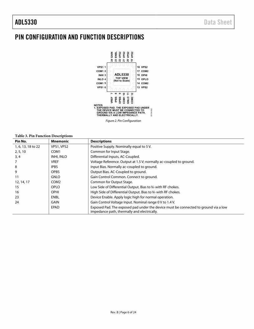
PIN CONFIGURATION AND FUNCTION DESCRIPTIONS
GA
INEN
BL
VPS2
VPS2
VPS2
VPS2
VPS2COM2OPLOOPHICOM2VPS2
CO
M2
GN
LOC
OM
1O
PBS
IPB
SVR
EF
VPS1COM1INLOINHI
COM1VPS1
0513
4-00
2
21
3456
181716151413
8 9 10 117 12
20 1921222324
ADL5330TOP VIEW
(Not to Scale)
NOTES1. EXPOSED PAD. THE EXPOSED PAD UNDER
THE DEVICE MUST BE CONNECTED TOGROUND VIA A LOW IMPEDANCE PATH,THERMALLY AND ELECTRICALLY.
Figure 2. Pin Configuration
Table 3. Pin Function Descriptions Pin No. Mnemonic Descriptions 1, 6, 13, 18 to 22 VPS1, VPS2 Positive Supply. Nominally equal to 5 V. 2, 5, 10 COM1 Common for Input Stage. 3, 4 INHI, INLO Differential Inputs, AC-Coupled. 7 VREF Voltage Reference. Output at 1.5 V; normally ac-coupled to ground. 8 IPBS Input Bias. Normally ac-coupled to ground. 9 OPBS Output Bias. AC-Coupled to ground. 11 GNLO Gain Control Common. Connect to ground. 12, 14, 17 COM2 Common for Output Stage. 15 OPLO Low Side of Differential Output. Bias to VP with RF chokes. 16 OPHI High Side of Differential Output. Bias to VP with RF chokes. 23 ENBL Device Enable. Apply logic high for normal operation. 24 GAIN Gain Control Voltage Input. Nominal range 0 V to 1.4 V. EPAD Exposed Pad. The exposed pad under the device must be connected to ground via a low
impedance path, thermally and electrically.
Data Sheet ADL5330
Rev. B | Page 7 of 24
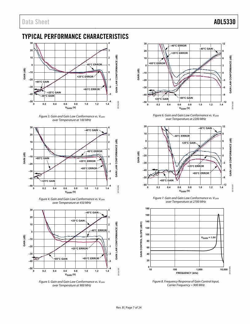
TYPICAL PERFORMANCE CHARACTERISTICS
0513
4-00
3G
AIN
LA
W C
ON
FOR
MA
NC
E (d
B)
–4
4
1
2
3
–1
0
–2
–3
VGAIN (V)1.40 0.2 0.4 0.6 0.8 1.0 1.2
GA
IN (d
B)
30
20
10
0
–10
–20
–30
–40
–50
+25°C GAIN
+85°C GAIN
–40°C ERROR
+25°C ERROR
+85°C ERROR
–40°C GAIN
Figure 3. Gain and Gain Law Conformance vs. VGAIN over Temperature at 100 MHz
0513
4-00
4G
AIN
LA
W C
ON
FOR
MA
NC
E (d
B)
–4
4
1
2
3
–1
0
–2
–3
VGAIN (V)1.40 0.2 0.4 0.6 0.8 1.0 1.2
GA
IN (d
B)
30
10
20
0
–20
–10
–40
–30
–50
–40°C GAIN
+25°C GAIN
+85°C GAIN
–40°C ERROR
+25°C ERROR
+85°C ERROR
Figure 4. Gain and Gain Law Conformance vs. VGAIN
over Temperature at 450 MHz
0513
4-00
5G
AIN
LA
W C
ON
FOR
MA
NC
E (d
B)
–4
4
2
1
3
0
–2
–1
–3
VGAIN (V)1.40 0.2 0.4 0.6 0.8 1.0 1.2
GA
IN (d
B)
30
20
10
0
–10
–20
–30
–40
–50
+25°C GAIN
–40°C GAIN
+85°C GAIN
–40°C ERROR
+25°C ERROR
+85°C ERROR
Figure 5. Gain and Gain Law Conformance vs. VGAIN
over Temperature at 900 MHz
0513
4-00
6G
AIN
LA
W C
ON
FOR
MA
NC
E (d
B)
–12
–9
12
3
6
9
–6
–3
0
VGAIN (V)1.40 0.2 0.4 0.6 0.8 1.0 1.2
GA
IN (d
B)
30
20
10
0
–10
–20
–30
–40
–50
–40°C GAIN
+25°C GAIN +85°C GAIN
–40°C ERROR
+25°C ERROR
+85°C ERROR
Figure 6. Gain and Gain Law Conformance vs. VGAIN
over Temperature at 2200 MHz
0513
4-00
7G
AIN
LA
W C
ON
FOR
MA
NC
E (d
B)
–12
12
0
3
6
9
–6
–3
–9
VGAIN (V)1.40 0.2 0.4 0.6 0.8 1.0 1.2
GA
IN (d
B)
20
10
0
–10
–20
–30
–40
–50
–60
–40°C GAIN
+25°C GAIN
+85°C GAIN
–40°C ERROR
+25°C ERROR
+85°C ERROR
Figure 7. Gain and Gain Law Conformance vs. VGAIN
over Temperature at 2700 MHz
0513
4-00
8
FREQUENCY (kHz)10,00010 100 1,000
GA
IN C
ON
TRO
L SL
OPE
(dB
/V)
180
140
160
100
120
60
80
40
20
0
VGAIN = 1.0V
Figure 8. Frequency Response of Gain Control Input, Carrier Frequency = 900 MHz
ADL5330 Data Sheet
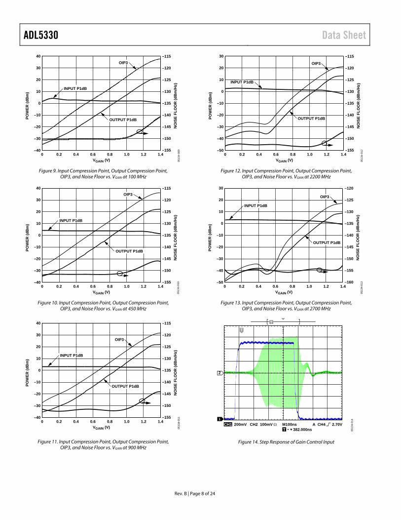
Rev. B | Page 8 of 24
0513
4-00
9N
OIS
E F
LO
OR
(d
Bm
/Hz)
–155
–115
–130
–125
–120
–145
–140
–135
–150
VGAIN (V)
1.40 0.2 0.4 0.6 0.8 1.0 1.2
PO
WE
R (
dB
m)
40
30
20
10
–10
0
–20
–30
–40
OIP3
INPUT P1dB
OUTPUT P1dB
Figure 9. Input Compression Point, Output Compression Point, OIP3, and Noise Floor vs. VGAIN at 100 MHz
0513
4-01
0N
OIS
E F
LO
OR
(d
Bm
/Hz)
–155
–115
–130
–125
–120
–145
–140
–135
–150
VGAIN (V)
1.40 0.40.2 0.80.6 1.0 1.2
PO
WE
R (
dB
m)
40
30
20
10
–10
0
–20
–30
–40
OIP3
OUTPUT P1dB
INPUT P1dB
Figure 10. Input Compression Point, Output Compression Point, OIP3, and Noise Floor vs. VGAIN at 450 MHz
0513
4-01
1N
OIS
E F
LO
OR
(d
Bm
/Hz)
–155
–115
–120
–125
–130
–135
–140
–145
–150
VGAIN (V)
1.40 0.40.2 0.6 0.8 1.0 1.2
PO
WE
R (
dB
m)
40
20
30
10
0
–10
–20
–30
–40
OIP3
INPUT P1dB
OUTPUT P1dB
Figure 11. Input Compression Point, Output Compression Point, OIP3, and Noise Floor vs. VGAIN at 900 MHz
0513
4-01
2N
OIS
E F
LO
OR
(d
Bm
/Hz)
–155
–115
–130
–125
–120
–150
–145
–140
–135
VGAIN (V)
1.40 0.2 0.4 0.6 0.8 1.0 1.2
PO
WE
R (
dB
m)
30
20
10
0
–10
–20
–30
–40
–50
INPUT P1dB
OIP3
OUTPUT P1dB
Figure 12. Input Compression Point, Output Compression Point, OIP3, and Noise Floor vs. VGAIN at 2200 MHz
0513
4-01
3N
OIS
E F
LO
OR
(d
Bm
/Hz)
–160
–155
–120
–140
–135
–130
–125
–150
–145
VGAIN (V)
1.40 0.2 0.4 0.6 0.8 1.0 1.2
PO
WE
R (
dB
m)
30
20
10
0
–10
–20
–30
–40
–50
INPUT P1dB
OIP3
OUTPUT P1dB
Figure 13. Input Compression Point, Output Compression Point, OIP3, and Noise Floor vs. VGAIN at 2700 MHz
0513
4-01
4
CH1 200mV CH2 100mV M100ns A CH4 2.70V
1
2
T 382.000ns
T
T
Figure 14. Step Response of Gain Control Input

Data Sheet ADL5330
Rev. B | Page 9 of 24
0513
4-01
5
VGAIN (V)1.40 0.2 0.4 0.6 0.8 1.0 1.2
OIP
3, O
P1dB
(dB
m)
40
30
20
10
0
–10
–20
–30
–40
–50
OP1dB (+25°C)
OP1dB (–40°C)
OP1dB (+85°C)
OIP3 (+25°C)
OIP3 (–40°C)
OIP3 (+85°C)
Figure 15. OP1dB and OIP3 vs. Gain over Temperature at 100 MHz
05
134-
016
VGAIN (V)1.40 0.2 0.4 0.6 0.8 1.0 1.2
OIP
3, O
P1dB
(dB
m)
40
20
30
10
–10
0
–30
–20
–40
OP1dB (+25°C)
OP1dB (–40°C)
OP1dB (+85°C)
OIP3 (+25°C)
OIP3 (–40°C)
OIP3 (+85°C)
Figure 16. OP1dB and OIP3 vs. Gain over Temperature at 450 MHz
0513
4-01
7
VGAIN (V)1.40 0.2 0.4 0.6 0.8 1.0 1.2
OIP
3, O
P1dB
(dB
m)
40
30
10
20
–10
0
–30
–20
–40
OP1dB (+25°C)
OP1dB (–40°C)
OP1dB (+85°C)
OIP3 (+25°C)
OIP3 (–40°C)
OIP3 (+85°C)
Figure 17. OP1dB and OIP3 vs. Gain over Temperature at 900 MHz
0513
4-01
8
VGAIN (V)1.40 0.2 0.4 0.6 0.8 1.0 1.2
OIP
3, O
P1dB
(dB
m)
30
10
20
–10
0
–30
–20
–40
–50
OP1dB (+25°C)OP1dB (–40°C)
OP1dB (+85°C)OIP3 (+25°C)
OIP3 (–40°C)
OIP3 (+85°C)
Figure 18. OP1dB and OIP3 vs. Gain over Temperature at 2200 MH z
0513
4-01
9
VGAIN (V)1.40 0.2 0.4 0.6 0.8 1.0 1.2
OIP
3, O
P1dB
(dB
m)
20
10
–10
0
–20
–40
–30
–50
OP1dB (+25°C)
OP1dB (–40°C)
OP1dB (+85°C)
OIP3 (+25°C)
OIP3 (–40°C)
OIP3 (+85°C)
Figure 19. OP1dB and OIP3 vs. Gain over Temperature at 2700 MHz
0513
4-02
0
VGAIN (V)1.40 0.2 0.4 0.6 0.8 1.0 1.2
I SU
PPLY
(mA
)
250
200
150
100
50
0
TEMP = +85°C
TEMP = +25°C
TEMP = –40°C
Figure 20. Supply Current vs. VGAIN and Temperature

ADL5330 Data Sheet
Rev. B | Page 10 of 24
0513
4-02
1
OP1dB (dBm)18.5 19 19.5 20.520 21 21.5 22 22.5 24.52423.523
PER
CEN
TAG
E (%
)
70
60
50
40
30
20
10
0
Figure 21. OP1dB Distribution at 900 MHz at Maximum Gain, VGAIN = 1.4 V
0513
4-02
2
OP1dB (dBm)9.5 10 10.5 11.511 12 12.5 13 13.5 1615 15.514.514
PER
CEN
TAG
E (%
)
30
25
20
15
10
5
0
Figure 22. OP1dB Distribution at 2200 MHz at Maximum Gain, VGAIN = 1.4 V
0513
4-02
3
OIP3 (dBm)
2828.5
29 3029.5 30.5
3131.5
3233.533.5 34.5
34 353332.5
PER
CEN
TAG
E (%
)
30
25
20
15
10
5
0
Figure 23. OIP3 Distribution at 900 MHz at Maximum Gain, VGAIN = 1.4 V
0513
4-02
4
OIP3 (dBm)
18.518 19 19.5 20 20.5 2422 2322.5 23.521.521
PER
CEN
TAG
E (%
)
30
25
20
15
10
5
0
Figure 24. OIP3 Distribution at 2200 MHz at Maximum Gain; VGAIN = 1.4 V
0513
4-02
5
FREQUENCY (MHz)10,00010 100 1,000
GA
IN (d
B)
30
20
10
0
–10
–20
–30
–40
–50
VGAIN = 0.2V
VGAIN = 0.4V
VGAIN = 0.6V
VGAIN = 0.8V
VGAIN = 1.0V
VGAIN = 1.2V
VGAIN = 1.4V
Figure 25. Gain vs. Frequency (Differential)
0513
4-02
6
FREQUENCY (MHz)10,00010 1,000100
GA
IN (d
B)
30
20
10
0
–10
–20
–30
–40
–50
VGAIN = 0.2V
VGAIN = 0.4V
VGAIN = 0.6V
VGAIN = 0.8V
VGAIN = 1.0V
VGAIN = 1.2V
VGAIN = 1.4V
Figure 26. Gain vs. Frequency (Using ETC1-1-13 Baluns)

Data Sheet ADL5330
Rev. B | Page 11 of 24
0180
30
330
60
90
270
300
120
240
150
210
0513
4-02
7
3GHz450MHz
1.9GHz
VGAIN = 1.2V
VGAIN = 0.2V
Figure 27. Input Impedance (Differential)
0513
4-02
9
FREQUENCY (MHz)100 600 1100 1600 2100 2600
S11
(dB
)
0
–5
–10
–15
–20
–25
–30
–35
Figure 28. Input Return Loss with ETC1-1-13 Baluns
0180
30
330
60
90
270
300
120
240
150
210
0513
4-02
8
1.9GHz
3GHz
450MHz
VGAIN = 1.2V VGAIN = 0.2V
Figure 29. Output Impedance (Differential)
0513
4-03
0
FREQUENCY (MHz)100 600 1100 1600 2100 2600
S11
(dB
)
0
–5
–10
–15
–20
–25
–30
–35
Figure 30. Output Return Loss with ETC1-1-13 Baluns
ADL5330 Data Sheet
Rev. B | Page 12 of 24
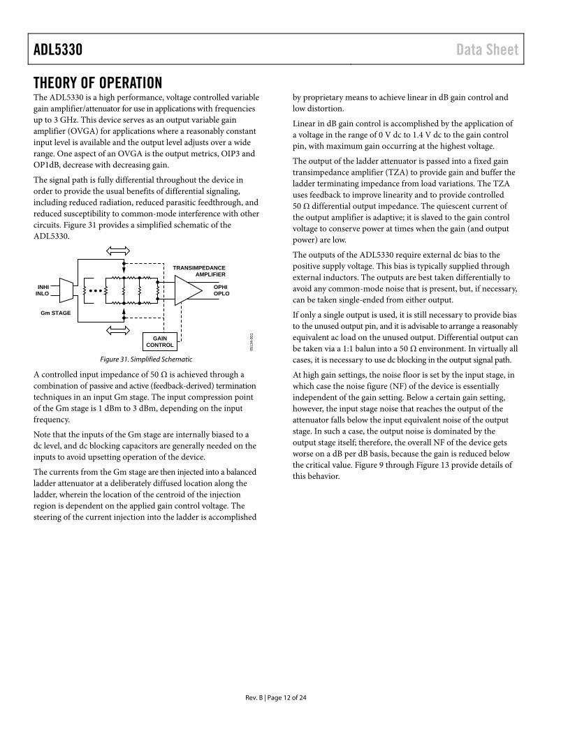
THEORY OF OPERATION The ADL5330 is a high performance, voltage controlled variable gain amplifier/attenuator for use in applications with frequencies up to 3 GHz. This device serves as an output variable gain amplifier (OVGA) for applications where a reasonably constant input level is available and the output level adjusts over a wide range. One aspect of an OVGA is the output metrics, OIP3 and OP1dB, decrease with decreasing gain.
The signal path is fully differential throughout the device in order to provide the usual benefits of differential signaling, including reduced radiation, reduced parasitic feedthrough, and reduced susceptibility to common-mode interference with other circuits. Figure 31 provides a simplified schematic of the ADL5330.
GAINCONTROL
0513
4-03
1
OPHIOPLO
INHIINLO
TRANSIMPEDANCEAMPLIFIER
Gm STAGE
Figure 31. Simplified Schematic
A controlled input impedance of 50 Ω is achieved through a combination of passive and active (feedback-derived) termination techniques in an input Gm stage. The input compression point of the Gm stage is 1 dBm to 3 dBm, depending on the input frequency.
Note that the inputs of the Gm stage are internally biased to a dc level, and dc blocking capacitors are generally needed on the inputs to avoid upsetting operation of the device.
The currents from the Gm stage are then injected into a balanced ladder attenuator at a deliberately diffused location along the ladder, wherein the location of the centroid of the injection region is dependent on the applied gain control voltage. The steering of the current injection into the ladder is accomplished
by proprietary means to achieve linear in dB gain control and low distortion.
Linear in dB gain control is accomplished by the application of a voltage in the range of 0 V dc to 1.4 V dc to the gain control pin, with maximum gain occurring at the highest voltage.
The output of the ladder attenuator is passed into a fixed gain transimpedance amplifier (TZA) to provide gain and buffer the ladder terminating impedance from load variations. The TZA uses feedback to improve linearity and to provide controlled 50 Ω differential output impedance. The quiescent current of the output amplifier is adaptive; it is slaved to the gain control voltage to conserve power at times when the gain (and output power) are low.
The outputs of the ADL5330 require external dc bias to the positive supply voltage. This bias is typically supplied through external inductors. The outputs are best taken differentially to avoid any common-mode noise that is present, but, if necessary, can be taken single-ended from either output.
If only a single output is used, it is still necessary to provide bias to the unused output pin, and it is advisable to arrange a reasonably equivalent ac load on the unused output. Differential output can be taken via a 1:1 balun into a 50 Ω environment. In virtually all cases, it is necessary to use dc blocking in the output signal path.
At high gain settings, the noise floor is set by the input stage, in which case the noise figure (NF) of the device is essentially independent of the gain setting. Below a certain gain setting, however, the input stage noise that reaches the output of the attenuator falls below the input equivalent noise of the output stage. In such a case, the output noise is dominated by the output stage itself; therefore, the overall NF of the device gets worse on a dB per dB basis, because the gain is reduced below the critical value. Figure 9 through Figure 13 provide details of this behavior.
Data Sheet ADL5330
Rev. B | Page 13 of 24
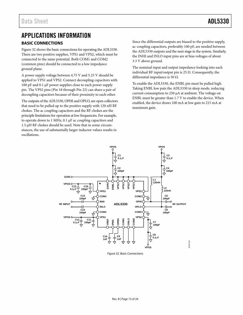
APPLICATIONS INFORMATION BASIC CONNECTIONS Figure 32 shows the basic connections for operating the ADL5330. There are two positive supplies, VPS1 and VPS2, which must be connected to the same potential. Both COM1 and COM2 (common pins) should be connected to a low impedance ground plane.
A power supply voltage between 4.75 V and 5.25 V should be applied to VPS1 and VPS2. Connect decoupling capacitors with 100 pF and 0.1 μF power supplies close to each power supply pin. The VPS2 pins (Pin 18 through Pin 22) can share a pair of decoupling capacitors because of their proximity to each other.
The outputs of the ADL5330, OPHI and OPLO, are open collectors that need to be pulled up to the positive supply with 120 nH RF chokes. The ac coupling capacitors and the RF chokes are the principle limitations for operation at low frequencies. For example, to operate down to 1 MHz, 0.1 μF ac coupling capacitors and 1.5 μH RF chokes should be used. Note that in some circum-stances, the use of substantially larger inductor values results in oscillations.
Since the differential outputs are biased to the positive supply, ac-coupling capacitors, preferably 100 pF, are needed between the ADL5330 outputs and the next stage in the system. Similarly, the INHI and INLO input pins are at bias voltages of about 3.3 V above ground.
The nominal input and output impedance looking into each individual RF input/output pin is 25 Ω. Consequently, the differential impedance is 50 Ω.
To enable the ADL5330, the ENBL pin must be pulled high. Taking ENBL low puts the ADL5330 in sleep mode, reducing current consumption to 250 μA at ambient. The voltage on ENBL must be greater than 1.7 V to enable the device. When enabled, the device draws 100 mA at low gain to 215 mA at maximum gain.
INHI
C13100pF
C11100pF
C120.1F
C101nF
C91nF
INLO
COM1
VPS1
VPS1
VR
EF
CO
M2
GN
LO
CO
M1
OP
BS
IPB
S
GA
IN
VP
S2
VP
S2
VP
S2
VP
S2
EN
BL
COM1
C14100pF
OPHI
C5100pF
OPLO
COM2
VPS2
VPS2
COM2
C6100pF
C7100pF
C80.1F
C10.1F
C2100pF
C16100pF
C120.1F
VPOS
GAIN
RF INPUT RF OUTPUT
VPOS
VPOS
VPOS
C30.1F
C4100pF
VPOS
L2120nH
L1120nH
ADL5330
0533
4-03
2
Figure 32. Basic Connections
ADL5330 Data Sheet
Rev. B | Page 14 of 24
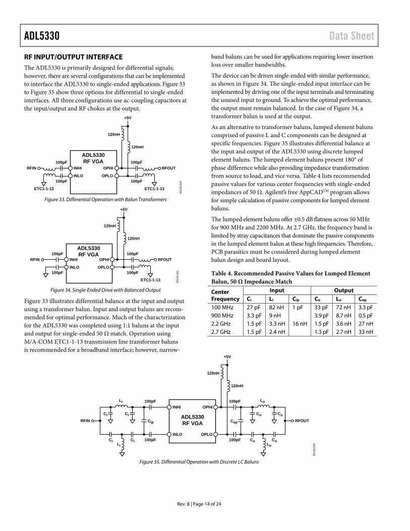
RF INPUT/OUTPUT INTERFACE The ADL5330 is primarily designed for differential signals; however, there are several configurations that can be implemented to interface the ADL5330 to single-ended applications. Figure 33 to Figure 35 show three options for differential to single-ended interfaces. All three configurations use ac-coupling capacitors at the input/output and RF chokes at the output.
RFIN
100pF
100pF
INHI
INLO
RFOUT
100pF
100pF
OPHI
OPLO
ADL5330RF VGA
120nH
120nH
+5V
0513
4-03
3
ETC1-1-13ETC1-1-13
Figure 33. Differential Operation with Balun Transformers
100pF
100pF
INHI
INLO
RFOUTRFIN
100pF
100pF
OPHI
OPLO
ADL5330RF VGA
120nH
120nH
+5V
ETC1-1-13
0513
4-04
1
Figure 34. Single-Ended Drive with Balanced Output
Figure 33 illustrates differential balance at the input and output using a transformer balun. Input and output baluns are recom-mended for optimal performance. Much of the characterization for the ADL5330 was completed using 1:1 baluns at the input and output for single-ended 50 Ω match. Operation using M/A-COM ETC1-1-13 transmission line transformer baluns is recommended for a broadband interface; however, narrow-
band baluns can be used for applications requiring lower insertion loss over smaller bandwidths.
The device can be driven single-ended with similar performance, as shown in Figure 34. The single-ended input interface can be implemented by driving one of the input terminals and terminating the unused input to ground. To achieve the optimal performance, the output must remain balanced. In the case of Figure 34, a transformer balun is used at the output.
As an alternative to transformer baluns, lumped element baluns comprised of passive L and C components can be designed at specific frequencies. Figure 35 illustrates differential balance at the input and output of the ADL5330 using discrete lumped element baluns. The lumped element baluns present 180° of phase difference while also providing impedance transformation from source to load, and vice versa. Table 4 lists recommended passive values for various center frequencies with single-ended impedances of 50 Ω. Agilent’s free AppCADTM program allows for simple calculation of passive components for lumped element baluns.
The lumped element baluns offer ±0.5 dB flatness across 50 MHz for 900 MHz and 2200 MHz. At 2.7 GHz, the frequency band is limited by stray capacitances that dominate the passive components in the lumped element balun at these high frequencies. Therefore, PCB parasitics must be considered during lumped element balun design and board layout.
Table 4. Recommended Passive Values for Lumped Element Balun, 50 Ω Impedance Match
Center Frequency
Input Output Ci Li Cip Co Lo Cop
100 MHz 27 pF 82 nH 1 pF 33 pF 72 nH 3.3 pF 900 MHz 3.3 pF 9 nH 3.9 pF 8.7 nH 0.5 pF 2.2 GHz 1.5 pF 3.3 nH 16 nH 1.5 pF 3.6 nH 27 nH 2.7 GHz 1.5 pF 2.4 nH 1.3 pF 2.7 nH 33 nH
INHI
INLO
RFOUT
100pF
Cop
Co Co
100pF Co CoLo
Lo
OPHI
OPLO
ADL5330RF VGA
120nH
120nH
+5V
RFIN
100pF
Cip
CiCi
100pFCiCiLi
Li
0513
4-03
5
Figure 35. Differential Operation with Discrete LC Baluns

Data Sheet ADL5330
Rev. B | Page 15 of 24
GAIN CONTROL INPUT When the VGA is enabled, the voltage applied to the GAIN pin sets the gain. The input impedance of the GAIN pin is 1 MΩ.
The gain control voltage range is between 0 V and +1.4 V, which corresponds to a typical gain range between −38 dB and +22 dB. The useful lower limit of the gain control voltage increases at high frequencies to about 0.5 V and 0.6 V for 2.2 GHz and 2.7 GHz, respectively. The supply current to the ADL5330 can vary from approximately 100 mA at low gain control voltages to 215 mA at 1.4 V.
The 1 dB input compression point remains constant at 3 dBm through the majority of the gain control range, as shown in Figure 9 through Figure 13. The output compression point increases dB for dB with increasing gain setting. The noise floor is constant up to 1 V where it begins to rise.
The bandwidth on the gain control pin is approximately 3 MHz. Figure 14 shows the response time of a pulse on the GAIN pin.
AUTOMATIC GAIN CONTROL Although the ADL5330 provides accurate gain control, precise regulation of output power can be achieved with an automatic gain control (AGC) loop. Figure 36 shows the ADL5330 in an AGC loop. The addition of the log amp (AD8318/AD8315) or a TruPwr™ detector (AD8362) allows the AGC to have improved temperature stability over a wide output power control range.
To operate the ADL5330 in an AGC loop, a sample of the output RF must be fed back to the detector (typically using a directional coupler and additional attenuation). A setpoint voltage is applied to the VSET input of the detector while VOUT is connected to the GAIN pin of the ADL5330. Based on the defined linear in dB relationship of the detector between VOUT and the RF input signal, the detector adjusts the voltage on the GAIN pin (the VOUT pin of the detector is an error amplifier output) until the level at the RF input corresponds to the applied setpoint voltage. The GAIN setting settles to a value that results in the correct balance between the input signal level at the detector and the setpoint voltage.
The error amplifier of the detector uses CFLT, a ground referenced capacitor pin, to integrate the error signal (in the form of a current). A capacitor must be connected to CFLT to set the loop bandwidth and to ensure loop stability.
INLO
INHI
GAIN
OPLO
OPHI
DIRECTIONALCOUPLER
ATTENUATOR
VPOS COMM
ADL5330
+5V +5V
CLPF
VOUT
VSET RFIN
LOG AMP ORTRUPWR
DETECTORDAC
0513
4-03
6
RFIN
Figure 36. ADL5330 in AGC Loop
The basic connections for operating the ADL5330 in an AGC loop with the AD8318 are shown in Figure 37. The AD8318 is a 1 MHz to 8 GHz precision demodulating logarithmic amplifier. It offers a large detection range of 60 dB with ±0.5 dB tempera-ture stability. This configuration is similar to Figure 36.
The gain of the ADL5330 is controlled by the output pin of the AD8318. This voltage, VOUT, has a range of 0 V to near VPOS. To avoid overdrive recovery issues, the AD8318 output voltage can be scaled down using a resistive divider to interface with the 0 V to 1.4 V gain control range of ADL5330.
A coupler/attenuation of 23 dB is used to match the desired maximum output power from the VGA to the top end of the linear operating range of the AD8318 (at approximately −5 dBm at 900 MHz).
ADL5330 Data Sheet
Rev. B | Page 16 of 24
INLO
INHI
GAIN
OPLO
OPHI
DIRECTIONALCOUPLER
ATTENUATOR
VPOS COMM
ADL5330
+5V
+5V
+5V
COMM
VOUT VPOS
VSET INHI
INLOCLPF
AD8318LOG AMP
DAC
RF INPUTSIGNAL
RF OUTPUTSIGNAL
412
1k
SETPOINTVOLTAGE
220pF
1nF
1nF
120nH120nH
100pF
100pF
0513
4-03
7
100pF
100pF
Figure 37. ADL5330 Operating in an Automatic Gain Control Loop in Combination with the AD8318
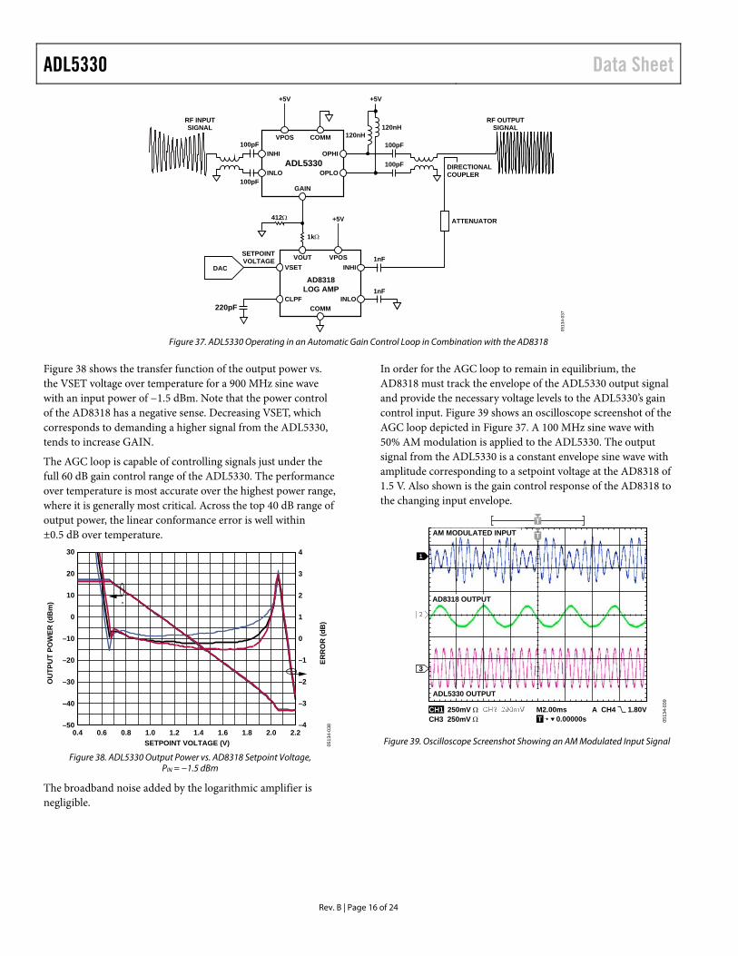
Figure 38 shows the transfer function of the output power vs. the VSET voltage over temperature for a 900 MHz sine wave with an input power of −1.5 dBm. Note that the power control of the AD8318 has a negative sense. Decreasing VSET, which corresponds to demanding a higher signal from the ADL5330, tends to increase GAIN.
The AGC loop is capable of controlling signals just under the full 60 dB gain control range of the ADL5330. The performance over temperature is most accurate over the highest power range, where it is generally most critical. Across the top 40 dB range of output power, the linear conformance error is well within ±0.5 dB over temperature.
0513
4-03
8E
RR
OR
(d
B)
–4
4
3
2
1
0
–1
–2
–3
SETPOINT VOLTAGE (V)
2.20.4 0.6 0.8 1.0 1.2 1.4 1.6 1.8 2.0
OU
TP
UT
PO
WE
R (
dB
m)
30
20
10
0
–10
–20
–30
–40
–50
Figure 38. ADL5330 Output Power vs. AD8318 Setpoint Voltage,
PIN = −1.5 dBm
The broadband noise added by the logarithmic amplifier is negligible.
In order for the AGC loop to remain in equilibrium, the AD8318 must track the envelope of the ADL5330 output signal and provide the necessary voltage levels to the ADL5330’s gain control input. Figure 39 shows an oscilloscope screenshot of the AGC loop depicted in Figure 37. A 100 MHz sine wave with 50% AM modulation is applied to the ADL5330. The output signal from the ADL5330 is a constant envelope sine wave with amplitude corresponding to a setpoint voltage at the AD8318 of 1.5 V. Also shown is the gain control response of the AD8318 to the changing input envelope.
0513
4-03
9
AD8318 OUTPUT
CH1 250mV CH3 250mV
M2.00ms A CH4 1.80V
1
3
T 0.00000s
T
T
ADL5330 OUTPUT
AM MODULATED INPUT
Figure 39. Oscilloscope Screenshot Showing an AM Modulated Input Signal
Data Sheet ADL5330
Rev. B | Page 17 of 24
Figure 40 shows the response of the AGC RF output to a pulse on VSET. As VSET decreases to 1 V, the AGC loop responds with an RF burst. Response time and the amount of signal integration are controlled by the capacitance at the AD8318 CFLT pin—a function analogous to the feedback capacitor around an integrating amplifier. An increase in the capacitance results in slower response time.
0513
4-04
0
CH1 2.00V CH2 50.0mV M10.0s A CH1 2.60V
2
1
T 20.2000s
T
AD8318 WITH PULSED VSET
ADL5330 OUTPUT
T
Figure 40. Oscilloscope Screenshot Showing the
Response Time of the AGC Loop
More information on the use of AD8318 in an AGC application can be found in the AD8318 data sheet.
INTERFACING TO AN IQ MODULATOR The basic connections for interfacing the AD8349 with the ADL5330 are shown in Figure 42. The AD8349 is an RF quadrature modulator with an output frequency range of 700 MHz to 2.7 GHz. It offers excellent phase accuracy and amplitude balance, enabling high performance direct RF modulation for communication systems.
The output of the AD8349 is designed to drive 50 Ω loads and easily interfaces with the ADL5330. The input to the ADL5330
can be driven single-ended, as shown in Figure 42. Similar con-figurations are possible with the AD8345 (250 MHz to 1 GHz) and AD8346 (800 MHz to 2.5 GHz) quadrature modulators.
Figure 41 shows how output power, EVM, ACPR, and noise vary with the gain control voltage. VGAIN is varied from 0 V to 1.4 V. Figure 41 shows that the modulation generated by the AD8349 is a 1 GHz 64 QAM waveform with a 1 MHz symbol rate. The ACPR values are measured in 1 MHz bandwidths at 1.1 MHz and 2.2 MHz carrier offsets. Noise floor is measured at a 20 MHz carrier offset.
0513
4-04
2
VGAIN (V)
1.40 0.2 0.4 0.80.6 1.0 1.2
OU
TP
UT
PO
WE
R (
dB
m)
AC
PR
(d
Bm
) (1
MH
z B
AN
DW
IDT
H)
NO
ISE
(d
Bm
/Hz)
(2
0M
Hz
CA
RR
IER
OF
FS
ET
)
EV
M (
%)
20 4.5
0 4.0
–20 3.5
–40 3.0
–60 2.5
–80 2.0
–100 1.5
–120 1.0
–140 0.5
–160 0
EVM
OUTPUT POWER
ACPR 2.2MHz OFFSET
ACPR 1.1MHz OFFSET
NOISE FLOOR
Figure 41. AD8349 and ADL5330 Output Power, ACPR, EVM, and Noise vs.
VGAIN for a 1 GHz 64 QAM Waveform with 1 MHz Symbol Rate
The output of the AD8349 driving the ADL5330 should be limited to the range that provides the optimal EVM and ACPR performance. The power range is found by sweeping the output power of the AD8349 to find the best compromise between EVM and ACPR of the system. In Figure 41, the AD8349 output power is set to −15 dBm.
100pF
100pF
INHI
INLO
RF OUTPUT
100pF
100pF
OPHI
COMMVPOS
OPLO
ADL5330RF VGA
120nH
120nH
+5V
+5V
ETC1-1-13
LO
100pF
100pF 200
200
ETC1-1-13
IBBP
IBBN
QBBP
QBBN
VOUT
COMMVPOS
AD8349IQ MOD
+5V
GAIN CONTROL
DAC
DAC
DIFFERENTIAL I/QBASEBAND INPUTS
0513
4-03
4
Figure 42. AD8349 Quadrature Modulator and ADL5330 Interface
ADL5330 Data Sheet
Rev. B | Page 18 of 24
WCDMA TRANSMIT APPLICATION Figure 43 shows a plot of the output spectrum of the ADL5330 transmitting a single-carrier WCDMA signal (Test Model 1-64 at 2140 MHz). The carrier power output is approximately −9.6 dBm. The gain control voltage is equal to 1.4 V giving a gain of approximately 14.4 dB. At this power level, an adjacent channel power ratio of −65.61 dBc is achieved. The alternate channel power ratio of −71.37 dBc is dominated by the noise floor of the ADL5330.
0513
4-04
3
SPAN 24.6848MHzCENTER 2.14GHz 2.46848MHz/
A
1RM
EXT
–20
–40
–50
–30
–60
–70
–80
–90
–100
–110
–120
1 AVG
1 [T1] –29.78 dBm2.13996994 GHz
CH PWR –9.56 dBmACP Up –66.30 dBACP Low –65.61 dBALT1 Up –71.37 dBALT1 Low –72.79 dB
0.4 dB OFFSET
CL2CL2
CL1CL1
C0 C0
CU1 CU1
CU2
CU2
REF LVL–20dBm
–29.78dBm2.13996994GHz
MARKER 1 [T1] RBWVBWSWT
30kHz300kHz100ms
RF ATT
UNIT
0dB
dBm
Figure 43. Single-Carrier WCDMA Spectrum at 2140 MHz;
VGAIN = 1.4 V, PIN = −23 dBm
Figure 44 shows how ACPR and noise vary with different input power levels (gain control voltage is held at 1.4 V). At high power levels, both adjacent and alternate channel power ratios sharply increase. As output power drops, adjacent and alternate channel power ratios both reach minima before the measurement becomes dominated by the noise floor of the ADL5330. At this point, adjacent and alternate channel power ratios become approximately equal.
As the output power drops, the noise floor, measured in dBm/Hz at 50 MHz carrier offset, initially falls and then levels off.
05
134-
044
NO
ISE
– dB
m @
50M
Hz
CA
RR
IER
OFF
SET
(1M
Hz
BW
)
–90
–50
–55
–60
–65
–70
–75
–80
–85
OUTPUT POWER (dBm)10–40 –35 –30 –25 –20 –15 –10 –5 0 5
AD
JAC
ENT/
ALT
ERN
ATE
CH
AN
NEL
POW
ER R
ATI
O (d
Bc)
–20
–30
–40
–50
–60
–70
–80
–90
–100
ACPR +5MHZ OFFSET
ACPR +10MHZOFFSET
NOISE –50MHz OFFSET
Figure 44. ACPR and Noise vs. Output Power; Single-Carrier
WCDMA Input (Test Model 1-64 at 2140 MHz), VGAIN = 1.4 V (Fixed)
Figure 45 shows how output power, ACPR, and noise vary with the gain control voltage. VGAIN is varied from 0 V to 1.4 V and input power is held constant at −19 dBm.
0513
4-04
5
AC
PR (d
Bc)
NO
ISE
@ 5
0MH
z O
FFSE
T (1
MH
z B
W)
–100
–20
–30
–40
–50
–60
–70
–80
–90
VGAIN (V)1.40.4 0.5 0.6 0.7 0.8 0.9 1.0 1.1 1.2 1.3
OU
TPU
T PO
WER
(dB
m)
10
0
–10
–20
–30
–40
–50
–60
–70
NOISE –50MHz OFFSET
OUTPUT POWER
ACPR 5MHz
ACPR 10MHz
Figure 45. Output Power, ACPR, and Noise vs. VGAIN;
Single-Carrier WCDMA (Test Model 1-64 at 2140 MHz) Input at −19 dBm

Data Sheet ADL5330
Rev. B | Page 19 of 24
CDMA2000 TRANSMIT APPLICATION To test the compliance to the CDMA2000 base station standard, an 880 MHz, three-carrier CDMA2000 test model signal (forward pilot, sync, paging, and six traffic, as per 3GPP2 C.S0010-B, Table 6.5.2.1) was applied to the ADL5330. A cavity-tuned filter with a 4.6 MHz pass band was used to reduce noise from the signal source being applied to the device.
Figure 46 shows the spectrum of the output signal under nominal conditions. Total POUT of the three-carrier signal is equal to 0.46 dBm and VGAIN = 1.4 V. Adjacent and alternate channel power ratio is measured in a 30 kHz bandwidth at 750 kHz and 1.98 MHz carrier offset, respectively.
0513
4-04
6
SPAN 15MHzCENTER 880MHz 1.5MHz/
A
1RM
EXT
–10
–30
–40
–20
–50
–60
–70
–80
–90
–100
–110
1 AVG
1 [T1] –18.55dBm880MHz
CH PWR 0.46dBmACP Up –65.13dBACP Low –64.40dBALT1 Up –89.05dBALT1 Low –83.68dBALT2 Up –80.72dBALT2 Low –81.24dB
1
CU3CU3
CU2CU2CU1
CU1CL1CL1CL2
CL2CL3CL3
C0C0
0.4 dB OFFSET
REF LVL–10dBm
MARKER 1 [T1]
–18.55dBm880.00000000MHz
RBW 30kHzVBW 300kHzSWT 200ms
RF ATT 10dBMIXER –10dBmUNIT dBm
Figure 46. 880 MHz Output Spectrum, Three-Carrier CDMA2000 Test Model at −23 dBm Total Input Power, VGAIN = 1.4 V, ACPR Measured at 750 kHz and
1.98 MHz Carrier Offset, Input Signal Filtered Using a Cavity Tuned Filter (Pass Band = 4.6 MHz)
In testing, by holding the gain control voltage steady at 1.4 V, input power was swept. Figure 47 shows ACPR and noise floor vs. total output power. Noise floor is measured at 1 MHz bandwidth at 4 MHz carrier offset.
0513
4-04
7
NO
ISE
– dB
m @
4M
Hz
CA
RR
IER
OFF
SET
(1M
Hz
RB
W)
–90
–0
–10
–20
–30
–40
–50
–60
–70
–80
TOTAL OUTPUT POWER (dBm)15–30 –25 –20 –15 –10 –5 0 5 10
AC
PR–
dBc
(30k
Hz
RB
W)
–30
–50
–40
–60
–70
–80
–90
–100
–110
–120
NOISE 4MHz OFFSET
ACPR 750kHz OFFSET
ACPR 1.98MHz OFFSET
Figure 47. ACPR vs. Total Output Power, 880 MHz Three-Carrier CDMA2000 Test Model; VGAIN = 1.4 V (Fixed), ACPR Measured in 30 kHz Bandwidth at
750 kHz and 1.98 MHz Carrier Offset
The results show that up to a total output power of +8 dBm, ACPR remains in compliance with the standard (<−45 dBc at 750 kHz and <−60 dBc at 1.98 MHz). At low output power levels, ACPR at 1.98 MHz carrier offset degrades as the noise floor of the ADL5330 becomes the dominant contributor to measured ACPR. Measured noise at 4 MHz carrier offset begins to increase sharply above 0 dBm output power. This increase is not due to noise but results from increased carrier-induced distortion. As output power drops below 0 dBm total, the noise floor drops towards −85 dBm.
With a fixed input power of −23 dBm, the output power was again swept by exercising the gain control input. VGAIN was swept from 0 V to 1.4 V. The resulting total output power, ACPR, and noise floor are shown in Figure 48.
0513
4-04
8
AC
PR (d
Bc)
NO
ISE
– 4M
Hz
CA
RR
IER
OFF
SET
– (1
MH
z R
BW
)
–100
–30
–40
–50
–60
–70
–80
–90
VGAIN (V)1.40 0.2 0.4 0.6 0.8 1.0 1.2
TOTA
L O
UTP
UT
POW
ER (d
Bm
)
10
0
–10
–20
–30
–40
–50
–60NOISE 4MHz OFFSET
ACPR 750kHz OFFSET
ACPR 1.98MHz OFFSET
OUTPUT POWER
Figure 48. Total Output Power and ACPR vs. VGAIN, 880 MHz Three-Carrier CDMA2000 Test Model at −23 dBm Total Input Power; ACPR Measured in
30 kHz Bandwidth at 750 kHz and 1.98 MHz Carrier Offset
Above VGAIN = 0.4 V, the ACPR is still in compliance with the standard. As the gain control input drops below 1.0 V, the noise floor drops below −90 dBm.
SOLDERING INFORMATION On the underside of the chip scale package, there is an exposed compressed paddle. This paddle is internally connected to the chip’s ground. Solder the paddle to the low impedance ground plane on the printed circuit board to ensure specified electrical performance and to provide thermal relief. It is also recommended that the ground planes on all layers under the paddle be stitched together with vias to reduce thermal impedance.
ADL5330 Data Sheet
Rev. B | Page 20 of 24
EVALUATION BOARD Figure 49 shows the schematic of the ADL5330 evaluation board. The silkscreen and layout of the component and circuit sides are shown in Figure 50 through Figure 53. The board is powered by a single-supply in the 4.75 V to 5.25 V range. The power supply is decoupled by 100 pF and 0.1 μF capacitors at each power supply pin. Additional decoupling, in the form of a series resistor or inductor at the supply pins, can also be added. Table 5 details the various configuration options of the evaluation board.
The output pins of the ADL5330 require supply biasing with 120 nH RF chokes. Both the input and output pins have 50 Ω differential impedances and must be ac-coupled. These pins are converted to single-ended with a pair of baluns (M/A-COM part number ETC1-1-13).
Instead of using balun transformers, lumped-element baluns comprising passive L and C components can be designed. Alternate input and output RF paths with component pads are available on the circuit side of the board. Components M1
through M9 are used for the input interface, and M10 through M18 are used for the output interface. DC blocking capacitors of 100 pF must be installed in C15 and C16 for the input and C17 and C18 for the output. The C5, C6, C11, and C12 capacitors must be removed. An alternate set of SMA connectors, INPUT2 and OUT2, are used for this configuration.
The ADL5330 can be driven single-ended; use the RF input path on the circuit side of the board. A set of 100 pF dc blocking capacitors must be installed in C15 and C16. C5 and C6 must be removed. Use the INPUT2 SMA to drive one of the differential input pins. The unused pin should be terminated to ground, as shown in Figure 34.
The ADL5330 is enabled by applying a logic high voltage to the ENBL pin by placing a jumper across the SW1 header in the O position. Remove the jumper for disable. This pulls the ENBL pin to ground through the 10 kΩ resistor.
Data Sheet ADL5330
Rev. B | Page 21 of 24
INH
I
C4
100p
FC
30.
1µF
R10 1nF
R11
1nF
INLO
CO
M1
VPS1
VPS1
VREF
COM2
GNLO
COM1
OPBS
IPBS
GAIN
VPS2
VPS2
VPS2
VPS2
ENBL
CO
M1
OPH
I
OPL
O
CO
M2
VPS2
VPS2
CO
M2
C10
100p
F
C9
0.1µ
F
C7
100p
FC
510
0pF
C6
100p
F
C16
OPE
N
C15
OPE
NM
4O
PEN
M9
OPE
N
M6
OPE
N
M5
OPE
N
C8
0.1 µ
F
VPO
S
GA
IN VPO
S
VPO
S
VREF
C2
0.1µ
F
C1
100p
F
VPO
S
C14
0.1µ
F
C13
100p
F
VPO
S
L212
0nH
L1 120n
H
AD
L533
0R2
0ΩR
12 0Ω
R13
10kΩ
VPO
S
R1
0Ω
R5
0Ω
R3
0Ω
R4
0Ω
R8
0Ω
R15
OPE
NR
70Ω
R14
OPE
N
SMA
IPB
S
R9
0ΩIP
BS
T1
M7
OPE
N
M3
OPE
N
M8
OPE
N
M1
OPE
N
M2
OPE
N
INPU
T2
INPU
T
C11
100p
F
C12
100p
F
C18
OPE
N
C17
OPE
NM
12O
PEN
M15
OPE
N
M10
OPE
N
M11
OPE
N
T2
M17
OPE
NM13
OPE
N
M16
OPE
N
M14
OPE
N M18
OPE
N
OU
T2
OU
T
0513
4-04
9
R6
0Ω
SW1
Figure 49. Evaluation Board Schematic

ADL5330 Data Sheet
Rev. B | Page 22 of 24
Table 5. Evaluation Board Configuration Options Components Function Default Conditions C1 to C4, C7 to C10, C13, C14, R2, R4, R5, R6, R12
Power Supply Decoupling. The nominal supply decoupling consists of 100 pF and 0.1 μF capacitors at each power supply pin (the VPS2 pins, Pin 18 to Pin 22, share a pair of decoupling capacitors because of their proximity). A series inductor or small resistor can be placed between the capacitors for additional decoupling.
C1, C4, C7, C10, C13 = 100 pF (size 0603)
C2, C3, C8, C9, C14 = 0.1 μF (size 0603)
R2, R4, R5, R6, R12 = 0 Ω (size 0402)
T1, C5, C6 Input Interface. The 1:1 balun transformer T1 converts a 50 Ω single-ended input to the 50 Ω differential input. C5 and C6 are dc blocks.
T1 = ETC1-1-13 (M/A-COM) C5, C6 = 100 pF (size 0603)
T2, C11, C12, L1, L2 Output Interface. The 1:1 balun transformer T2 converts the 50 Ω differential output to 50 Ω single-ended output. C11 and C2 are dc blocks. L3 and L4 provide dc biases for the output.
T2 = ETC1-1-13 (M/A-COM) C11, C12 = 100 pF (size 0603) L1, L2 = 120 nH (size 0805)
SW1, R1, R13 Enable Interface. The ADL5330 is enabled by applying a logic high voltage to the ENBL pin by placing a jumper across SW1 to the O position. Remove the jumper for disable. To exercise the enable function by applying an external high or low voltage, use the pin labeled O on the SW1 header.
SW1 = installed R1 = 0 Ω (size 0402) R13 = 10 kΩ (size 0402)
C15 to C18, M1 to M18 Alternate Input/Output Interface. The circuit side of the evaluation board offers an alternate RF input and output interface. A lumped-element balun can be built using L and C components instead of using the balun transformer (see the Applications Information section). The components, M1 through M9, are used for the input, and M10 through M18 are used for the output. To use the alternate RF paths, disconnect the dc blocking capacitors (Capacitor C5 and Capacitor C6 for the input and Capacitor C11 and Capacitor C12 for the output). Place 100 pF dc blocking capacitors on C15, C16, C17, and C18. Use the alternate set of SMA connectors, INPUT2 and OUT2.
M1 to M18 = not installed (size 0603)
C15 to C18 = not installed (size 0603)

Data Sheet ADL5330
Rev. B | Page 23 of 24
051
34-
051
Figure 50. Component Side Silkscreen
051
34-0
50
Figure 51. Circuit Side Silkscreen
0513
4-05
3
Figure 52. Component Side Layout
0513
4-05
2
Figure 53. Circuit Side Layout
ADL5330 Data Sheet
Rev. B | Page 24 of 24
OUTLINE DIMENSIONS
0.800.750.70
PK
G-0
03
99
4/5
111
0.50BSC
0.500.400.30
COMPLIANT TO JEDEC STANDARDS MO-220-WGGD-8
BOTTOM VIEWTOP VIEW
4.104.00 SQ3.90
0.05 MAX0.02 NOM
0.203 REF
COPLANARITY0.08
PIN 1INDICATOR
1
24
712
13
18
19
6
03-0
9-2
017
-B
0.300.250.20
0.20 MIN
2.442.30 SQ2.16
EXPOSEDPAD
SEATINGPLANE
PIN 1INDIC ATOR AREA OPTIONS(SEE DETAIL A)
DETAIL A(JEDEC 95)
FOR PROPER CONNECTION OFTHE EXPOSED PAD, REFER TOTHE PIN CONFIGURATION ANDFUNCTION DESCRIPTIONSSECTION OF THIS DATA SHEET.
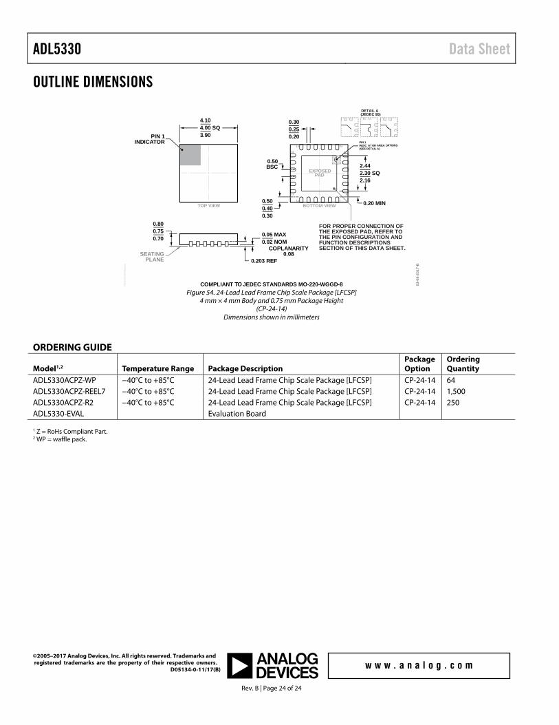
Figure 54. 24-Lead Lead Frame Chip Scale Package [LFCSP]
4 mm × 4 mm Body and 0.75 mm Package Height (CP-24-14)
Dimensions shown in millimeters
ORDERING GUIDE
Model1,2 Temperature Range Package Description Package Option
Ordering Quantity
ADL5330ACPZ-WP −40°C to +85°C 24-Lead Lead Frame Chip Scale Package [LFCSP] CP-24-14 64 ADL5330ACPZ-REEL7 −40°C to +85°C 24-Lead Lead Frame Chip Scale Package [LFCSP] CP-24-14 1,500 ADL5330ACPZ-R2 −40°C to +85°C 24-Lead Lead Frame Chip Scale Package [LFCSP] CP-24-14 250 ADL5330-EVAL Evaluation Board 1 Z = RoHs Compliant Part. 2 WP = waffle pack.
©2005–2017 Analog Devices, Inc. All rights reserved. Trademarks and registered trademarks are the property of their respective owners. D05134-0-11/17(B)