.(10 + 10W Min. @ D = 1%) HIGH OUTPUT POWER HIGH CURRENT ... · TDA2009A 10 +10W STEREO AMPLIFIER...
12
TDA2009A 10 +10W STEREO AMPLIFIER September 2003 PIN CONNECTION MULTIWATT11 ORDERING NUMBER : TDA2009A ® . HIGH OUTPUT POWER (10 + 10W Min. @ D = 1%) . HIGH CURRENT CAPABILITY (UP TO 3.5A) . AC SHORT CIRCUIT PROTECTION . THERMAL OVERLOAD PROTECTION . SPACE AND COST SAVING : VERY LOW NUMBER OF EXTERNAL COMPONENTS AND SIMPLE MOUNTING THANKS TO THE MULTIWATT PACKAGE. DESCRIPTION The TDA2009A is class AB dual Hi-Fi Audio power amplifier assembled in Multiwatt package, spe- cially designed for high quality stereo application as Hi-Fi and music centers. 1/12
Transcript of .(10 + 10W Min. @ D = 1%) HIGH OUTPUT POWER HIGH CURRENT ... · TDA2009A 10 +10W STEREO AMPLIFIER...
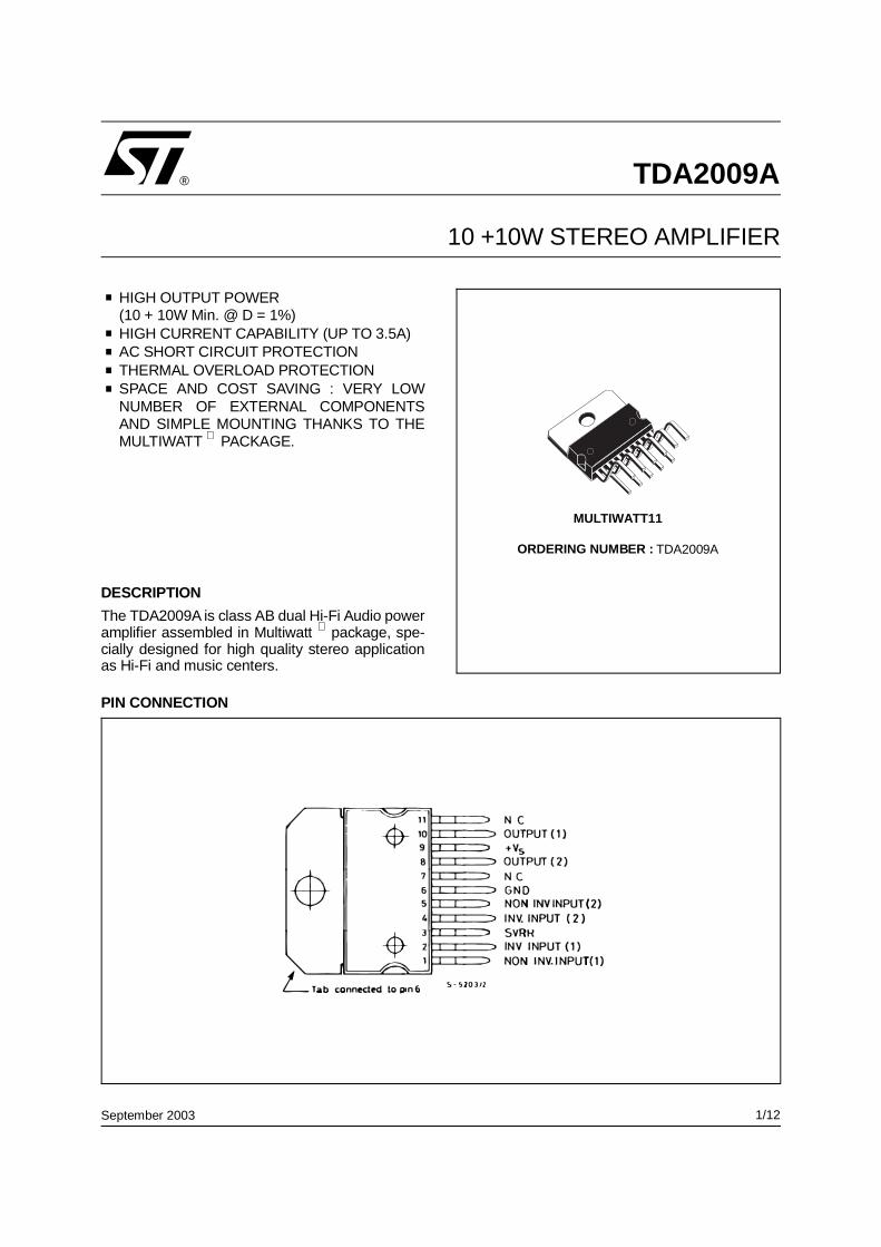
TDA2009A
10 +10W STEREO AMPLIFIER
September 2003
PIN CONNECTION
MULTIWATT11
ORDERING NUMBER : TDA2009A
®
.HIGH OUTPUT POWER(10 + 10W Min. @ D = 1%).HIGH CURRENT CAPABILITY (UP TO 3.5A).AC SHORT CIRCUIT PROTECTION.THERMAL OVERLOAD PROTECTION.SPACE AND COST SAVING : VERY LOWNUMBER OF EXTERNAL COMPONENTSAND SIMPLE MOUNTING THANKS TO THEMULTIWATT PACKAGE.
DESCRIPTION
The TDA2009A is class AB dual Hi-Fi Audio poweramplifier assembled in Multiwatt package, spe-cially designed for high quality stereo applicationas Hi-Fi and music centers.
1/12
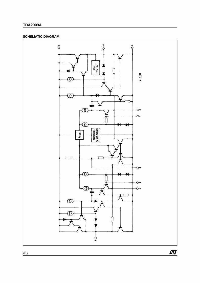
SCHEMATIC DIAGRAM
TDA2009A
2/12
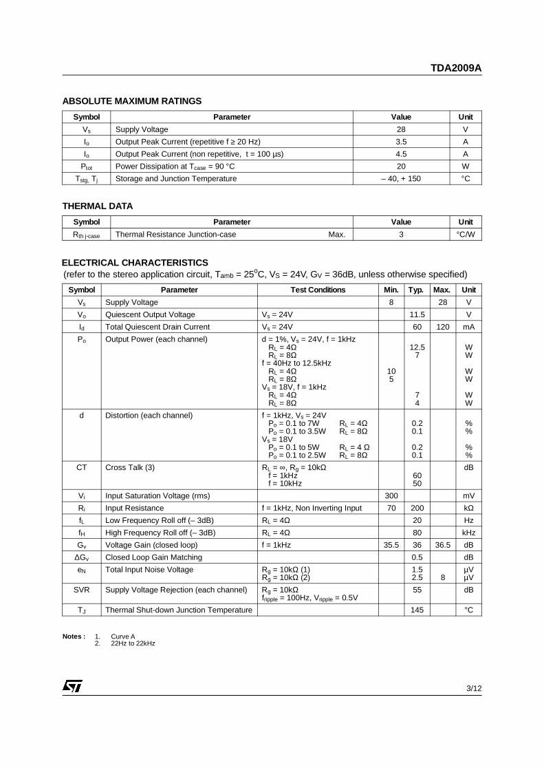
ABSOLUTE MAXIMUM RATINGS
Symbol Parameter Value Unit
Vs Supply Voltage 28 V
Io Output Peak Current (repetitive f ≥ 20 Hz) 3.5 A
Io Output Peak Current (non repetitive, t = 100 µs) 4.5 A
Ptot Power Dissipation at Tcase = 90 °C 20 W
Tstg, Tj Storage and Junction Temperature – 40, + 150 °C
THERMAL DATA
Symbol Parameter Value Unit
Rth j-case Thermal Resistance Junction-case Max. 3 °C/W
ELECTRICAL CHARACTERISTICS(refer to the stereo application circuit, Tamb = 25oC, VS = 24V, GV = 36dB, unless otherwise specified)
Symbol Parameter Test Conditions Min. Typ. Max. Unit
Vs Supply Voltage 8 28 V
Vo Quiescent Output Voltage Vs = 24V 11.5 V
Id Total Quiescent Drain Current Vs = 24V 60 120 mA
Po Output Power (each channel) d = 1%, Vs = 24V, f = 1kHzRL = 4ΩRL = 8Ω
f = 40Hz to 12.5kHzRL = 4ΩRL = 8Ω
Vs = 18V, f = 1kHzRL = 4ΩRL = 8Ω
105
12.57
74
WW
WW
WW
d Distortion (each channel) f = 1kHz, Vs = 24VPo = 0.1 to 7W RL = 4ΩPo = 0.1 to 3.5W RL = 8Ω
Vs = 18VPo = 0.1 to 5W RL = 4 ΩPo = 0.1 to 2.5W RL = 8Ω
0.20.1
0.20.1
%%
%%
CT Cross Talk (3) RL = ∞, Rg = 10kΩf = 1kHzf = 10kHz
6050
dB
Vi Input Saturation Voltage (rms) 300 mV
Ri Input Resistance f = 1kHz, Non Inverting Input 70 200 kΩfL Low Frequency Roll off (– 3dB) RL = 4Ω 20 Hz
fH High Frequency Roll off (– 3dB) RL = 4Ω 80 kHz
Gv Voltage Gain (closed loop) f = 1kHz 35.5 36 36.5 dB
∆Gv Closed Loop Gain Matching 0.5 dB
eN Total Input Noise Voltage Rg = 10kΩ (1)Rg = 10kΩ (2)
1.52.5 8
µVµV
SVR Supply Voltage Rejection (each channel) Rg = 10kΩfripple = 100Hz, Vripple = 0.5V
55 dB
TJ Thermal Shut-down Junction Temperature 145 °C
Notes : 1. Curve A2. 22Hz to 22kHz
TDA2009A
3/12
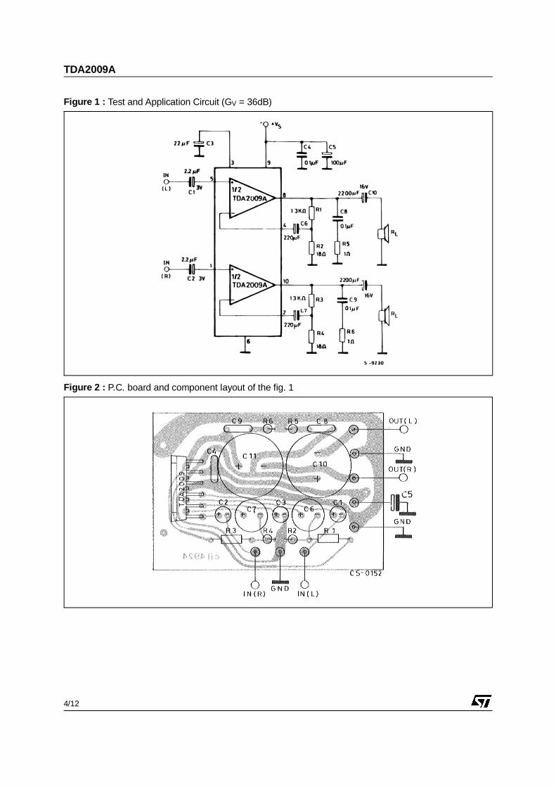
Figure 1 : Test and Application Circuit (GV = 36dB)
Figure 2 : P.C. board and component layout of the fig. 1
TDA2009A
4/12
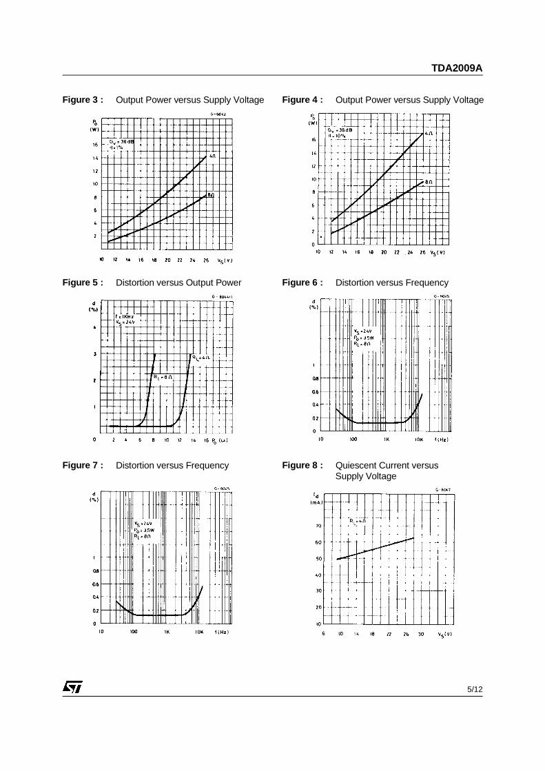
Figure 3 : Output Power versus Supply Voltage Figure 4 : Output Power versus Supply Voltage
Figure 5 : Distortion versus Output Power Figure 6 : Distortion versus Frequency
Figure 7 : Distortion versus Frequency Figure 8 : Quiescent Current versusSupply Voltage
TDA2009A
5/12
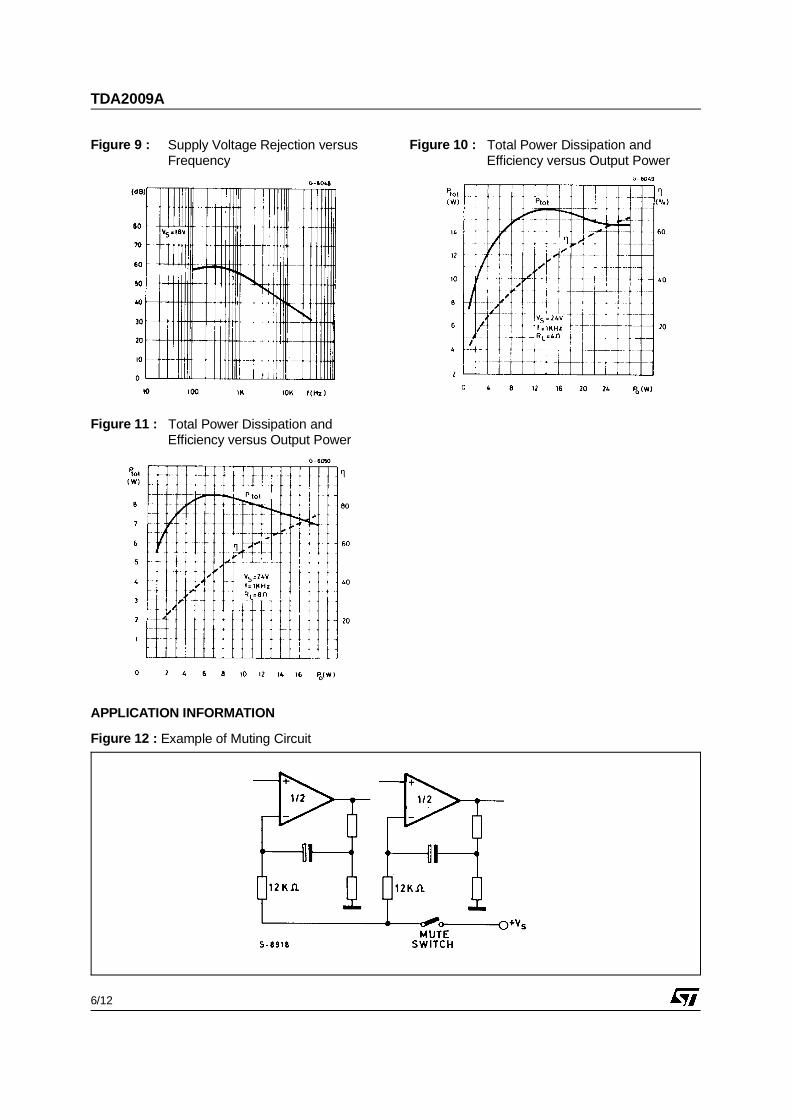
Figure 9 : Supply Voltage Rejection versusFrequency
Figure 10 : Total Power Dissipation andEfficiency versus Output Power
Figure 11 : Total Power Dissipation andEfficiency versus Output Power
APPLICATION INFORMATION
Figure 12 : Example of Muting Circuit
TDA2009A
6/12

Figure 13 : 10W +10W Stereo Amplifier with Tone Balance and Loudness Control
Figure 14 : Tone Control Response(circuit of Figure 13)
TDA2009A
7/12
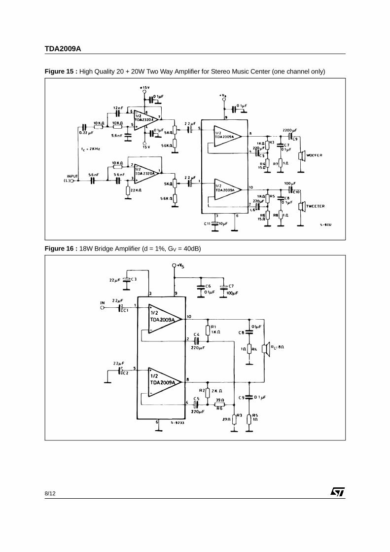
Figure 15 : High Quality 20 + 20W Two Way Amplifier for Stereo Music Center (one channel only)
Figure 16 : 18W Bridge Amplifier (d = 1%, GV = 40dB)
TDA2009A
8/12
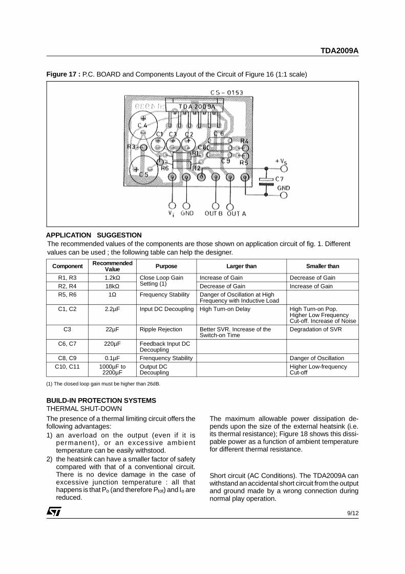
Figure 17 : P.C. BOARD and Components Layout of the Circuit of Figure 16 (1:1 scale)
APPLICATION SUGGESTIONThe recommended values of the components are those shown on application circuit of fig. 1. Differentvalues can be used ; the following table can help the designer.
Component RecommendedValue Purpose Larger than Smaller than
R1, R3 1.2kΩ Close Loop GainSetting (1)
Increase of Gain Decrease of GainR2, R4 18kΩ Decrease of Gain Increase of GainR5, R6 1Ω Frequency Stability Danger of Oscillation at High
Frequency with Inductive LoadC1, C2 2.2µF Input DC Decoupling High Turn-on Delay High Turn-on Pop.
Higher Low FrequencyCut-off. Increase of Noise
C3 22µF Ripple Rejection Better SVR. Increase of theSwitch-on Time
Degradation of SVR
C6, C7 220µF Feedback Input DCDecoupling
C8, C9 0.1µF Frenquency Stability Danger of OscillationC10, C11 1000µF to
2200µFOutput DCDecoupling
Higher Low-frequencyCut-off
(1) The closed loop gain must be higher than 26dB.
The presence of a thermal limiting circuit offers thefollowing advantages:1) an averload on the output (even if it is
permanent), or an excessive ambienttemperature can be easily withstood.
2) the heatsink can have a smaller factor of safetycompared with that of a conventional circuit.There is no device damage in the case ofexcessive junction temperature : all thathappens is that Po (and therefore Ptot) and Io arereduced.
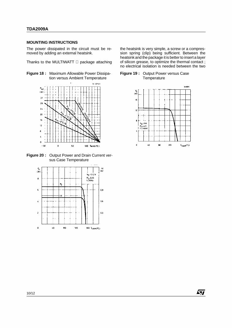
The maximum allowable power dissipation de-pends upon the size of the external heatsink (i.e.its thermal resistance); Figure 18 shows this dissi-pable power as a function of ambient temperaturefor different thermal resistance.
Short circuit (AC Conditions). The TDA2009A canwithstand an accidental short circuit from the outputand ground made by a wrong connection duringnormal play operation.
BUILD-IN PROTECTION SYSTEMSTHERMAL SHUT-DOWN
TDA2009A
9/12
The power dissipated in the circuit must be re-moved by adding an external heatsink.
Thanks to the MULTIWATT package attaching
the heatsink is very simple, a screw or a compres-sion spring (clip) being sufficient. Between theheatsink and the package it is better to insert a layerof silicon grease, to optimize the thermal contact ;no electrical isolation is needed between the two
MOUNTING INSTRUCTIONS
Figure 18 : Maximum Allowable Power Dissipa-tion versus Ambient Temperature
Figure 19 : Output Power versus CaseTemperature
Figure 20 : Output Power and Drain Current ver-sus Case Temperature
TDA2009A
10/12
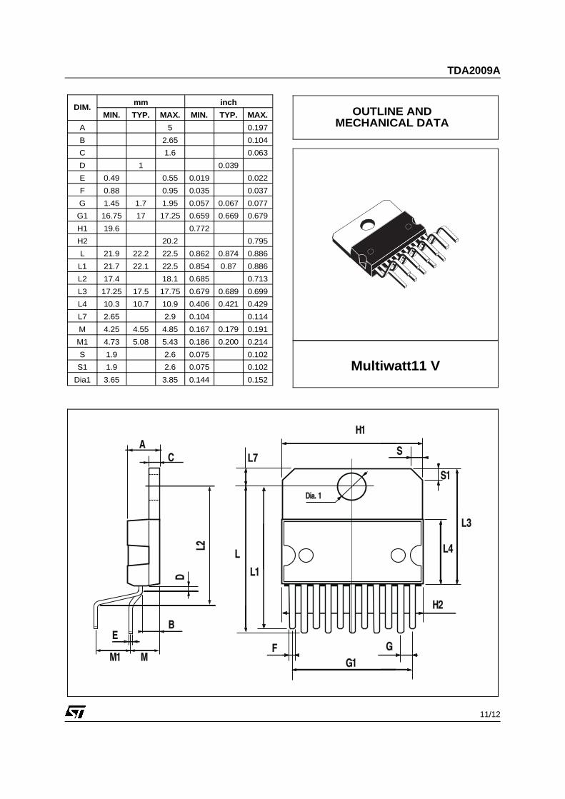
Multiwatt11 V
DIM.mm inch
MIN. TYP. MAX. MIN. TYP. MAX.
A 5 0.197
B 2.65 0.104
C 1.6 0.063
D 1 0.039
E 0.49 0.55 0.019 0.022
F 0.88 0.95 0.035 0.037
G 1.45 1.7 1.95 0.057 0.067 0.077
G1 16.75 17 17.25 0.659 0.669 0.679
H1 19.6 0.772
H2 20.2 0.795
L 21.9 22.2 22.5 0.862 0.874 0.886
L1 21.7 22.1 22.5 0.854 0.87 0.886
L2 17.4 18.1 0.685 0.713
L3 17.25 17.5 17.75 0.679 0.689 0.699
L4 10.3 10.7 10.9 0.406 0.421 0.429
L7 2.65 2.9 0.104 0.114
M 4.25 4.55 4.85 0.167 0.179 0.191
M1 4.73 5.08 5.43 0.186 0.200 0.214
S 1.9 2.6 0.075 0.102
S1 1.9 2.6 0.075 0.102
Dia1 3.65 3.85 0.144 0.152
OUTLINE ANDMECHANICAL DATA
TDA2009A
11/12
Information furnished is believed to be accurate and reliable. However, STMicroelectronics assumes no responsibility for theconsequences of use of such information nor for any infringement of patents or other rights of third parties which may result f romits use. No license is granted by implication or otherwise under any patent or patent rights of STMicroelectronics. Specificati onsmentioned in this publication are subject to change without notice. This publication supersedes and replaces all informationpreviously supplied. STMicroelectronics products are not authorized for use as critical components in life support devices or s ystemswithout express written approval of STMicroelectronics.
The ST logo is a registered trademark of STMicroelectronics.All other names are the property of their respective owners
© 2003 STMicroelectronics - All rights reserved
STMicroelectronics GROUP OF COMPANIESAustralia – Belgium - Brazil - Canada - China – Czech Republic - Finland - France - Germany - Hong Kong - India - Israel - Ital y - Ja-
pan - Malaysia - Malta - Morocco - Singapore - Spain - Sweden - Switzerland - United Kingdom - United Stateswww.st.com
TDA2009A
12/12