1. Visualization of the Silicon Crystal 2. Conductivity 3 ...
127
1. Visualization of the Silicon Crystal 2. Conductivity 3. Temperature Dependence of Semiconductor Conductivity 4. Electron and Hole Concentrations 5. The Concept of Mobility , FIELD DEPENDENCE 6. complete ionization 7. Effective masses and Fermi distribution Function 8. Energy: Density of States 9. Compounds 10. Transparent Semiconductors 11. THE DRIFT CURRENT , THE DIFFUSION CURRENT 12. continuity equation 13. p-n junction theory 14. ideal and Nonideal p-n Junction 15. The transition capacitance , The diffusion capacitance 16. photoelectric effect 17. Schottky Diode 18. solar cell
Transcript of 1. Visualization of the Silicon Crystal 2. Conductivity 3 ...

1. Visualization of the Silicon Crystal 2. Conductivity 3. Temperature Dependence of Semiconductor Conductivity 4. Electron and Hole Concentrations 5. The Concept of Mobility , FIELD DEPENDENCE 6. complete ionization 7. Effective masses and Fermi distribution Function 8. Energy: Density of States 9. Compounds 10. Transparent Semiconductors 11. THE DRIFT CURRENT , THE DIFFUSION CURRENT 12. continuity equation 13. p-n junction theory 14. ideal and Nonideal p-n Junction 15. The transition capacitance , The diffusion capacitance 16. photoelectric effect 17. Schottky Diode 18. solar cell

Part (1) Solved PROBLEMS Visualization of the Silicon Crystal
Example (1):
Write the electronic configuration of silicon has 14 electrons in its atom,
determine in which sub shell and in which orbit and how many electrons in
the highest sub shell energy.
Solution:
The electronic configuration of silicon as follows,
1S2 2S2 2p6 3S2 3p2
The highest sub shell energy lies in (M) orbit, in the sub shell (p) which
is not fully occupied , it has only 2 electrons
Example (2):
Write the electronic configuration of iodine (I) has 53 electrons in its
atom, determine in which sub shell and in which orbit and how many
electrons in the highest sub shell energy.
Solution:
The electronic configuration of iodine (I) as follows,
1S2 2S2 2p6 3S2 3p6 3D10 4S2 4p6 4D10 4F7
The highest sub shell energy lies in (N) orbit, in the sub shell (F) is not
fully occupied, it has only seven electrons
Example (3):
Write the electronic configuration of Tantalum 73 has 73 electrons in its
atom, determine in which sub shell and in which orbit and how many
electrons in the highest sub shell energy.

Solution:
The electronic configuration of iodine (I) as follows,
1S2 2S2 2p6 3S2 3p6 3D10 4S2 4p6 4D10 4F14 5S2 5p6 5D5
The highest sub shell energy lies in (O) orbit, in the sub shell (D) which
is not fully occupied, it has only 5 electrons
Example (4) :
Write the electron configuration of silicon in its following energy states
14Si+. 14Si+2, 14Si+3 .
Solution:
From tables, the atomic number for silicon is 14, which means, it has 14
electrons in its steady state distributed among orbits and sub shells.
Therefore, the electron configuration in the following energy states
14Si+. 14Si+2, 14Si+3 can be represented as,
14Si+ has 14-1=13 electrons
1s22s22p63s23p1
14Si+2 has 14-2=12 electrons
1s22s22p63s2
14Si+3 has 14-3=11 electrons
1s22s22p63s1
Problem 1 The expression for the Bohr radius can also be applied to the hydrogen-like atom consisting of an ionized donor and the electron provided by the donor. Modify the expression for the Bohr radius so that it applies to this hydrogen-like atom. Calculate the resulting radius of an electron orbiting around
the ionized donor in silicon. (𝝐𝒓 = 11.9 and µe* = 0.26 µ0) Solution The Bohr radius is obtained from:

𝒂𝒐 = 𝝐𝒐𝒉
𝟐𝒏𝟐
𝒑 𝝁𝟎𝒒𝟐
However, since the electron travel through silicon one has to replace the permittivity of vacuum with the dielectric constant of silicon and the free electron mass with the effective mass for conductivity calculations so that:
𝒂𝒐, 𝒅𝒐𝒏𝒐𝒓 𝒊𝒏 𝒔𝒊𝒍𝒊𝒄𝒐𝒏 = 𝒂𝒐𝝐𝒓𝝁𝒆∗𝝁𝟎
= 𝟓𝟐𝟗 𝒙 𝟏𝟏. 𝟗
𝟎. 𝟐𝟔 𝒑𝒎 = 𝟐. 𝟒𝟐 𝒏𝒎
Problem 2 Electron mobility in Si is 1400 cm2 V−1s−1. Calculate the mean free time in scattering, (Relaxationszeit) of electrons. Effective mass is m*e/m0 = 0.33. Solution: (1.3)
From μ = eτ/m* we get that τ = 2.6 × 10⁻¹³ s. Problem 3 Calculate thermal velocity of electrons and holes in GaAs at room temperature. Effective masses are m*e/m0 = 0.063 and m*h/m0 = 0.53. Solution:
𝒗𝒕 = ∫ 𝒗 𝒆𝒙𝒑 (– 𝒎∗ 𝒗
𝟐
𝟐 𝑲𝑻⁄ ) 𝒅𝟑𝒗∞
𝟎
∫ 𝒆𝒙𝒑 (– 𝒎∗ 𝒗𝟐
𝟐 𝑲𝑻⁄ ) 𝒅𝟑𝒗∞
𝟎
= √𝟖 𝑲𝑻
𝝅 𝒎∗
Thermal velocities of electrons and holes are 4.3 × 10⁷ and 1.5 × 107 cm/s, respectively.
Problem 4 Calculate dielectric relaxation time in p-type Ge at room temperature. Assume that all acceptors are ionized. Na = 1015 cm−3, ε = 16, μp = 1900 cm2 V−1s−1.

Solution: (1.6)
τr = ε/4 πe Na μp = 4.7 × 10⁻¹² s. Problem 5 Calculate dielectric relaxation time in intrinsic Si at 300 K. ε = 12, μn = 1400 cm2 V−1s−1, μn = 3.1 μp. Solution: In this case,
𝝉𝒕 = 𝝐
𝟒 𝝅 𝒆 𝒏𝒊 (𝝁𝒏 + 𝝁𝒑)= 𝟑. 𝟒 𝒙 𝟏𝟎−𝟕 𝒔
Problem 6 Calculate the ambipolar diffusion coefficient of intrinsic (undoped) Ge at 300 K. μn/μp = 2.1, μn = 3900 cm2 V−1s−1. Solution: D = 65 cm2/s.
Problem 7 Holes are injected into n-type Ge so that at the sample surface Δp0 = 1014 cm−3. Calculate Δp at the distance of 4 mm
from the surface if τp = 10−3 s and Dp = 49 cm2/s. Solution:
∆ 𝒑 = ∆𝒑𝒐 𝒙 𝒆𝒙𝒑(− 𝑳
√𝑫𝒑𝝉𝒑) = 𝟏. 𝟔 𝒙 𝟏𝟎𝟏𝟑 𝒄𝒎−𝟑
Problem 8 What is the width of an infinite quantum well if the second lowest energy of a free electron confined to the well equals 100 meV? Solution

The second lowest energy is calculated from
𝑬𝟐 = 𝒉𝟐
𝟐 𝒎∗(𝟐
𝟐 𝑰𝒙)𝟐
= 𝟏. 𝟔 𝒙𝟏𝟎−𝟐𝟎 𝑱
One can therefore solve for the width, Lx, of the well, yielding:
𝑰𝒙 = 𝒉
√𝟐 𝒎∗𝑬𝟐=
𝟔. 𝟔𝟐𝟔 𝒙 𝟏𝟎−𝟑𝟒
√𝟐 𝒙𝟗. 𝟏𝟏 𝒙 𝟏𝒐−𝟑𝟏𝒙𝟏. 𝟔 𝒙𝟏𝟎−𝟐𝟎= 𝟑. 𝟖𝟖 𝒏𝒎
Problem 9 Calculate the lowest three possible energies of an electron in a hydrogen atom in units of electron volt. Identify all possible electron energies between the lowest energy and -2 eV. Solution The three lowest electron energies in a hydrogen atom can be calculated from
𝑬𝒏 = − 𝟏𝟑. 𝟔 𝒆𝑽
𝒏𝟐 𝒘𝒊𝒕𝒉 𝒏 = 𝟏 . 𝟐 , 𝒂𝒏𝒅 𝟑
resulting in: E1 = –13.6 eV, E2 = -3.4 eV and E3 = -1.51 eV The second lowest energy, E2, is the only one between the lowest energy, E1, and –2 eV.
Problem 9 Calculate the maximum fraction of the volume in a simple cubic crystal occupied by the atoms. Assume that the atoms are closely packed and that they can be treated as hard spheres. This fraction is also called the packing density. Solution: The atoms in a simple cubic crystal are located at the corners of the units cell, a cube with side a. Adjacent atoms touch each other so that the radius of each atom equals a/2.

There are eight atoms occupying the corners of the cube, but only one eighth of each is within the unit cell so that the number of atoms equals one per unit cell. The packing density is then obtained from:
𝐯𝐨𝐥𝐮𝐦𝐞 𝐨𝐟 𝐚𝐭𝐨𝐦𝐬
𝐯𝐨𝐥𝐮𝐦𝐞 𝐨𝐟 𝐮𝐧𝐢𝐭 𝐜𝐞𝐥𝐥=
𝟒
𝟑 𝐩 𝐫𝟑
𝐚𝟑=
𝟒
𝟑 𝐩 (
𝐚
𝟐)𝟑
𝐚𝟑= 𝛒
𝟔= 𝟓𝟐%
or about half the volume of the unit cell is occupied by the atoms. The packing density of four cubic crystals is listed in the table below. Radius Atoms/
unit cell
Packing density
Simple cubic 𝒂𝟐⁄ 1 𝝆
𝟔⁄ = 𝟓𝟐%
Body centered cubic √𝟑 𝒂𝟒⁄
2 𝝆√𝟑𝟖⁄ = 𝟔𝟖%
Face centered cubic √𝟐 𝒂𝟒⁄
4 𝝆√𝟐𝟔⁄ = 𝟕𝟒%
Diamond √𝟑 𝒂𝟖⁄
8 𝝆√𝟑𝟏𝟔⁄ = 𝟑𝟒%
Problem 10 Calculate the packing density of the body centered cubic, the face centered cubic and the diamond lattice, listed in example 2.1 p 28. Solution The packing density is calculated as obtained from:
𝐯𝐨𝐥𝐮𝐦𝐞 𝐨𝐟 𝐚𝐭𝐨𝐦𝐬
𝐯𝐨𝐥𝐮𝐦𝐞 𝐨𝐟 𝐮𝐧𝐢𝐭 𝐜𝐞𝐥𝐥=
𝟒
𝟑 𝐩 𝐫𝟑
𝐚𝟑
The correct radius and number of atoms per unit cell should be used. A body centered cubic lattice contains an additional atom in the middle and therefore contains two atoms per unit cell.
The atoms touch along the body diagonal, which equals √𝟑

a. The radius is one quarter of the body diagonal. A face centered cubic lattice contains six additional atoms in the center of all six faces of the cube. Since only half of the atoms is within the cube the total number of atoms per unit cell equals four. The atoms touch along the diagonal of the
faces of the cube, which equals √𝟐a . The radius is one quarter of the diagonal. The diamond lattice contains two face centered cubic lattice so that the total number of atoms per unit cell equals twice that of the face centered lattice, namely eight. The atoms touch along the body diagonal, where two atoms are one
quarter of the body diagonal apart or √𝟑 a/4 . The radius equals half the distance between the two atoms. The radius, number of atoms per unit cell and the packing density are summarized in the table below. Radius Atoms/
unit cell
Packing density
Simple cubic 𝒂𝟐⁄ 1 𝝆
𝟔⁄ = 𝟓𝟐%
Body centered cubic √𝟑 𝒂𝟒⁄
2 𝝆√𝟑𝟖⁄ = 𝟔𝟖%
Face centered cubic √𝟐 𝒂𝟒⁄
4 𝝆√𝟐𝟔⁄ = 𝟕𝟒%
Diamond √𝟑 𝒂𝟖⁄
8 𝝆√𝟑𝟏𝟔⁄ = 𝟑𝟒%
Problem 11 Electrons in undoped gallium arsenide have a mobility of 8,800 cm2/V-s. Calculate the average time between collisions. Calculate the distance traveled between two collisions (also called the mean free path). Use an average velocity of 107
cm/s. Solution The collision time, tc, is obtained from:

𝒕𝒄 = 𝒎𝒏𝒎𝒆
∗
𝒒= 𝟎. 𝟖𝟖 𝒙 𝟎. 𝟎𝟔𝟕 𝒙 𝟗. 𝟏 𝒙 𝟏𝟎−𝟑𝟐
𝟏. 𝟔 𝒙 𝟏𝟎−𝟏𝟗= 𝟎. 𝟑𝟒 𝒑𝒔
𝒍 = 𝝂𝒂𝒗𝒂𝒓𝒂𝒈𝒆𝒕𝒄 = 𝟏𝟎𝟕 𝒙 𝒐. 𝟑𝟒 𝒙 𝟏𝟎−𝟏𝟐 = 𝟑𝟒 𝒏𝒎
Problem 12 Calculate dielectric relaxation time in p-type Ge at room temperature. Assume that all acceptors are ionized. Na = 1015 cm−3, ϵ = 16, µp = 1900 cm2 V−1s−1. Solution:
𝝉𝒓 = 𝝐
𝟒 𝝅 𝒆 𝑵𝒂𝝁𝒑= 𝟒. 𝟕 𝒙 𝟏𝟎−𝟏𝟐 𝒔
Problem 13 Calculate dielectric relaxation time in intrinsic Si at 300 K. ϵ = 12, µn = 1400 cm2 V−1s−1, µn = 3.1µp. Solution: In this case
𝝉𝒓 = 𝝐
𝟒 𝝅 𝒆 𝒏𝒊 (𝝁𝒏 + 𝝁𝒑)= 𝟑. 𝟒 𝒙 𝟏𝟎−𝟕 𝒔
Part (2) Solved PROBLEMS conductivity Example (1) Calculate the conductivity and the resistivity of n-type silicon wafer which contains 1016 electrons per cubic centimeter with an electron mobility of 1400 cm2/Vs. Solution: The conductivity is obtained by adding the product of the electronic charge, q, the carrier mobility, and the density of carriers of each carrier type, or:
𝝈 = 𝒒 (𝒏 𝝁𝒏 + 𝒑 𝝁𝒑)
As n-type material contains almost no holes, the conductivity equals:

𝝈 = 𝒒 𝒏 𝝁𝒏 = 𝟏. 𝟔 𝒙 𝟏𝟎−𝟏𝟗 𝒙 𝟏𝟒𝟎𝟎 𝒙 𝟏𝟎𝟔 = 𝟐. 𝟐𝟒 𝟏𝛀𝒄𝒎
The resistivity equals the inverse of the conductivity or:
𝝆 = 𝟏
𝝈 =
𝟏
𝒒 (𝒏 𝝁𝒏 + 𝒑 𝝁𝒑)
and equals ρ = 1/ σ = 1/2.24 = 0.446 Ω cm. Example (2) An n-type piece of silicon of length L = 10 micron has a cross sectional area A= 0.001 cm2. A voltage V = 10 Volts applied across the sample yielding a current I = 100 mA. What is the resistance, R of the silicon sample, its conductivity, σ , and electron density, n? μn= 1400 cm2/Vs Solution The resistance of the sample equals R = V/I = 10/0.1 = 100 Ω. Since R = L /(σA)the conductivity is obtained from: σ = L/(R A) = 0.001/(100 x 0.001) = 0.01 1/ Ω cm. The required electron density is related to the conductivity by: σ = q n μn so that the density equals: n = σ/(qμn) = 0.01/(1.6 x 10-19x 1400) = 4.46 x 1013cm-3. Example (3) A silicon wafer contains 1018cm-3phosphor atoms. Using the data in the table;
Arsenic Phosphorus Boron
μmin(𝒎𝟐𝑽−𝟏𝒔−𝟏) 52.2 68.5 44.9
μmax(𝒎𝟐𝑽−𝟏𝒔−𝟏) 1417 1414 470.5
Ni (cm-3) 9.68 x 10¹⁶ 9.20 x 10¹⁶ 2.23 x 10¹⁷
α 0.68 0.711 0.719 Calculate the resistivity and conductivity of the material. Repeat for arsenic and boron atoms. Solution Plugging the values from table into the following equation,
𝝁 = 𝝁𝒎𝒊𝒏 + 𝝁𝒎𝒂𝒙 − 𝝁𝒎𝒊𝒏
𝟏 + (𝑵
𝑵𝒊) 𝜶
one obtains a mobility of 277 cm2/V-sec for phosphorus-doped material, 284 cm2/V-sec for arsenic-doped material and 153 cm2/V-sec for boron-doped material, corresponding to a resistivity of 22.6, 22.0

and 40.9 mΩ .cm and a conductivity of 44.3, 45.4 and 24.5 1/Ω cm.
Example 4 Estimate the electrical conductivity of intrinsic silicon at 300 K, given that the electron and hole motilities are0.15 m2 /V-s and 0.05 m2 /V-s. Solution The conductivity arises due to both electrons and holes
𝝈 = 𝒒 𝒏𝒊(𝝁𝒆 + 𝝁𝒉) The intrinsic carrier concentration was calculated to be at 300 K. Thus
𝝈 = 𝟏. 𝟔 𝒙 𝟏𝟎−𝟏𝟗 𝒙 𝟏. 𝟐 𝒙 𝟏𝟎𝟏𝟔 𝒙 𝟎. 𝟐 = 𝟑. 𝟖𝟒 𝒙 𝟏𝟎−𝟒𝛀/𝒎
Exercise 5 A sample of an intrinsic semiconductor has a band gap of 0.7 eV, assumed independent of temperature. Taking µh = 0.5 µe and µh = 2 µe, find the relationship between the conductivity at 200 K and300 K. (Ans. ratio of conductivity = 2014.6 eV) EF (300 K) - EF (200 K) = 4.33 x 10⁻³ eV
Example 2.9 A piece of silicon doped with arsenic (Nd = 1017 cm-3) is 100 µm long, 10 µm wide and 1 µm thick. Calculate the resistance of this sample when contacted one each end. Solution The resistivity of the silicon equals:
𝝆 =𝟏
𝒒 𝒏 𝒎𝒙=
𝟏
𝟏. 𝟔 𝒙 𝟏𝟎−𝟏𝟗 𝒙 𝟏𝟎𝟏𝟕 𝒙 𝟕𝟐𝟕= 𝟎. 𝟎𝟖𝟔 𝛀 𝒄𝒎
where the mobility was obtained from Table . The resistance then equals

𝑹 = 𝝆 𝑳
𝒘𝒕= 𝟎. 𝟎𝟖𝟔 𝒙
𝟏𝟎𝟎 𝒙 𝟏𝟎−𝟒
𝟏𝟎𝟎 𝒙 𝟏𝟎−𝟒 𝒙𝟏𝟎−𝟒= 𝟖. 𝟔 𝑲𝛀
𝑹𝒔 = 𝝆
𝒕= 𝟎. 𝟎𝟖𝟔
𝟏𝟎−𝟒= 𝟖𝟔𝟎 𝛀/𝒔𝒒
From which one then obtains the resistance:
𝑹 = 𝑹𝒔𝑳
𝒘= 𝟖𝟔𝟎 𝒙
𝟏𝟎𝟎 𝒙 𝟏𝟎−𝟒
𝟏𝟎 𝒙 𝟏𝟎−𝟒= 𝟖. 𝟔 𝑲𝛀
Problem 2.13 The resistivity of a silicon wafer at room temperature is 5 Ωcm. What is the doping density? Find all possible solutions. Solution Starting with a initial guess that the conductivity is due to electrons with a mobility of 1400 cm2/V-s, the corresponding doping density equals:
𝑵𝑫 = 𝒏 = 𝟏
𝒒 𝝁𝒏𝝆=
𝟏
𝟏. 𝟔 𝒙 𝟏𝟎−𝟏𝟗 𝒙 𝟏𝟒𝟎𝟎 𝒙 𝟓= 𝟖. 𝟗 𝒙 𝟏𝟎𝟏𝟒𝒄𝒎−𝟑
The mobility corresponding to this doping density equals
𝝁𝒏 = 𝝁𝒎𝒂𝒙 + 𝝁𝒎𝒂𝒙 − 𝝁𝒎𝒊𝒏
𝟏 + (𝑵𝑫
𝑵𝝆)𝒂 = 𝟏𝟑𝟔𝟔 𝒄𝒎𝟐/𝒗𝒔
Since the calculated mobility is not the same as the initial guess, this process must be repeated until the assumed mobility is the same as the mobility corresponding to the calculated doping density, yielding: Nd = 9.12 x 1014 cm-3 and µn = 1365 cm2/V-s For p-type material one finds: Na = 2.56 x 1015 cm-3 and µp = 453 cm2/V-s Example 2.11
Calculate the electron and hole densities in an n-type silicon wafer (Nd = 1017 cm-3) illuminated uniformly with 10 mW/cm2 of red light (Eph = 1.8 eV). The absorption coefficient of red light in silicon is 10-
3 cm-1. The minority carrier lifetime is 10 ms.

Solution The generation rate of electrons and holes equals:
𝑮𝒏 = 𝑮𝒑 = ∝ 𝑷𝑶𝑷𝑻𝑬𝒑𝒉 𝒒
= 𝟏𝟎−𝟑 𝟏𝟎−𝟐
𝟏. 𝟖 𝒙 𝟏. 𝟔 𝒙 𝟏𝟎−𝟏𝟗= 𝟑. 𝟓 𝒙 𝟏𝟎𝟐𝟑 𝒄𝒎−𝟑𝒔−𝟏
Where, α is absorption coefficient, Popt illumination power , Ept is the red light , where the photon energy was converted into Joules. The excess carrier densities are then obtained from:
𝜹𝒏 = 𝜹𝒑 = 𝝉𝒑 𝑮𝒑 = 𝟏𝟎 𝒙 𝟏𝟎−𝟑 𝒙 𝟑. 𝟓 𝒙 𝟏𝟎𝟐𝟑 = 𝟑. 𝟓 𝒙 𝟏𝟎𝟐𝟏 𝒄𝒎−𝟑
The excess carrier densities are then obtained from: So that the electron and hole densities equal:
𝒏 = 𝒏𝒐 + 𝜹𝒏 = 𝟏𝟎𝟏𝟕 + 𝟑. 𝟓 𝒙 𝟏𝟎𝟐𝟏 = 𝟑. 𝟓 𝒙 𝟏𝟎𝟐𝟏𝒄𝒎−𝟑
Problem 2.14 How many phosphorus atoms must be added to decrease the resistivity of n-type silicon at room temperature from 1 Ω−cm to 0.1 Ω−cm. Make sure you include the doping dependence of the mobility. State your assumptions. Solution Starting with a initial guess that the conductivity is due to electrons with a mobility of 1400 cm2/V-s, the corresponding doping density corresponding to the initial resistivity of 1 Ω−cm equals:
𝑵𝑫 ≅ 𝒏 = 𝟏
𝒒 𝝁𝒏𝝆=
𝟏
𝟏. 𝟔 𝒙 𝟏𝟎−𝟏𝟗 𝒙 𝟏𝟒𝟎𝟎 𝒙 𝟏= 𝟒. 𝟒𝟔 𝒙 𝟏𝟎𝟏𝟓𝒄𝒎−𝟑
The mobility corresponding to this doping density equals
𝝁𝒏 = 𝝁𝒎𝒂𝒙 + 𝝁𝒎𝒂𝒙 − 𝝁𝒎𝒊𝒏
𝟏 + (𝑵𝑫
𝑵𝝆)𝒂 = 𝟏𝟐𝟕𝟒 𝒄𝒎𝟐/𝒗𝒔
Since the calculated mobility is not the same as the initial guess, this process must be repeated until the assumed

mobility is the same as the mobility corresponding to the calculated doping density, yielding:
Nd,initial = 4.94 x 1015 cm-3 and µn = 1265 cm2/V-s Repeating this procedure for a resistivity of 0.1 Ω−cm one find the final doping density to be
Nd,final = 8.08 x 1016 cm-3 and µn = 772 cm2/V-s The added density of phosphorous atoms therefore equals
Nd, added = 4.94 x 10¹⁵ - = 7.59 x 1016 cm-3
Problem 2.26 A piece of silicon has a resistivity which is specified by the manufacturer to be between 2 and 5 Ohm cm. Assuming that the mobility of electrons is 1400 cm2/V-sec and that of holes is 450 cm2/V-sec, what is the minimum possible carrier density and what is the corresponding carrier type? Repeat for the maximum possible carrier density. Solution The minimum carrier density is obtained for the highest resistivity and the material with the highest carrier mobility, i.e. the n-type silicon. The minimum carrier density therefore equals:
𝒏 = 𝟏
𝒒 𝝁𝒏𝝆𝒎𝒂𝒙=
𝟏
𝟏. 𝟔 𝒙 𝟏𝟎−𝟏𝟗 𝒙 𝟏𝟒𝟎𝟎𝒙 𝟓= 𝟖. 𝟗𝟐 𝒙 𝟏𝟎𝟏𝟒𝒄𝒎−𝟑
The maximum carrier density is obtained for the lowest resistivity and the material with the lowest carrier mobility, i.e. the p-type silicon. The maximum carrier density therefore equals:
𝒑 = 𝟏
𝒒 𝝁𝒑 𝝆𝒎𝒂𝒙=
𝟏
𝟏. 𝟔 𝒙 𝟏𝟎−𝟏𝟗 𝒙 𝟒𝟓𝟎𝒙 𝟐= 𝟔. 𝟗𝟒 𝒙 𝟏𝟎𝟏𝟓𝒄𝒎−𝟑
Problem 2.27 A silicon wafer has a 2-inch diameter and contains 1014 cm-3 electrons with a mobility of 1400 cm2/V-sec. How thick

should the wafer be so that the resistance between the front and back surface equals 0.1 Ohm? Solution The resistance is given by
𝑹 = 𝝆 𝑳
𝑨
Where A is the area of the wafer and L the thickness, so that the wafer thickness equals:
𝑳 = 𝑹 𝑨
𝝆= 𝟎. 𝟏 𝒙 𝒑 𝒙 (𝟐. 𝟓𝟒)𝟐
𝟒𝟒. 𝟔= 𝟎. 𝟒𝟓𝟓 𝒎𝒎
The resistivity, 𝝆, was obtained from:
𝝆 = 𝟏
𝒒 𝒏 𝝁𝒏=
𝟏
𝟏. 𝟔 𝒙 𝟏𝟎−𝟏𝟗 𝒙 𝟏𝟒𝟎𝟎𝒙 𝟏𝟎𝟏𝟒= 𝟒𝟒. 𝟔 𝛀 𝒄𝒎
Part (3) Solved PROBLEMS Temperature Dependence of Semiconductor Conductivity
Band gap of Si depends on the temperature as Eg = 1.17 eV − 4.73 × 10⁻⁴ T2 / T + 636 . Find a concentration of electrons in the conduction band of intrinsic (undoped) Si at T = 77 K if at 300 K ni = 1.05 × 1010 cm−3. Solution: (1.2)
𝒏𝒊𝟐 = 𝑵𝒄𝑵𝒗 𝒆𝒙𝒑 (−
𝑬𝒈
𝑲𝑻) ≈ 𝑻𝟑 𝐞𝐱𝐩 (−
𝑬𝒈
𝑲𝑻)
Therefore,
𝒏𝟏(𝑻𝟐) = 𝒏𝟏(𝑻𝟏) (𝑻𝟐𝑻𝟏)
𝟑𝟐⁄
𝐞𝐱𝐩 (− 𝑬𝒈𝑻𝟐
𝟐 𝑲 𝑻𝟐+𝑬𝒈𝑻𝟏
𝟐 𝑲 𝑻𝟏 )
Putting the proper values in the formula we obtain that
ni(77K) ≈ 10−20cm−3. 5. Hole mobility in Ge at room temperature is 1900 cm2 V−1s−1.

Find the diffusion coefficient. Solution: (1.5) From eD = μkT, it follows that D = 49 cm2/s.
Example 2.4b Calculate the intrinsic carrier density in germanium, silicon and gallium arsenide at 300, 400, 500 and 600 K. Solution The intrinsic carrier density in silicon at 300 K equals:
𝒏𝒊(𝟑𝟎𝟎𝑲) = √𝑵𝒄𝑵𝒗 𝒆𝒙𝒑 (− 𝑬𝒈
𝟐 𝑲𝑻)
= √𝟐. 𝟖𝟏 𝒙 𝟏𝟎𝟏𝟗 𝒙 𝟏. 𝟖𝟑 𝒙 𝟏𝟎𝟏𝟗 𝒆𝒙𝒑 (− 𝟏. 𝟏𝟐
𝟐 𝒙 𝟎. 𝟎𝟐𝟓𝟖)
= 𝟖. 𝟕𝟐 𝒙 𝟏𝟎𝟗𝒎−𝟑 Similarly, one finds the intrinsic carrier density for germanium and gallium arsenide at different temperatures, yielding:
Germanium Silicon Gallium Arsenide
300 K 2.02 x 10¹³ 8.72 x 10⁹ 2.03 x 10⁶
400 K 1.38 x 10¹⁵ 4.52 x 10¹² 5.98 x 10⁹
500 K 1.91 x 10¹⁶ 2.16 x 10¹⁴ 7.98 x 10¹¹
600 K 1.18 x 10¹⁷ 3.07 x 10¹⁵ 2.22 x 10¹³
Example 2.2 Calculate the energy band gap of germanium, silicon and gallium arsenide at 300, 400, 500 and 600 K. Solution The band gap of silicon at 300 K equals:
𝑬𝒈(𝟑𝟎𝟎 𝒌) = 𝑬𝒈(𝟎 𝒌) − 𝒂 𝑻𝟐
𝑻 + 𝒃= 𝟏. 𝟏𝟔𝟔 −
𝟎. 𝟒𝟕𝟑 𝒙 𝟏𝟎−𝟑 𝒙 (𝟑𝟎𝟎)𝟐
𝟑𝟎𝟎 + 𝟔𝟑𝟔= 𝟏. 𝟏𝟐 𝒆𝑽
Similarly, one finds the energy band gap for germanium and

gallium arsenide, as well as at different temperatures, yielding:
Germanium Silicon Gallium Arsenide
T = 300 K 0.66 eV 1.12 eV 1.42 eV
T = 400 K 0.62 eV 1.09 eV 1.38 eV
T = 500 K 0.58 eV 1.06 eV 1.33 eV
T = 600 K 0.54 eV 1.03 eV 1.28 eV
Problem 2.2 At what temperature does the energy band gap of silicon equal exactly 1 eV? Solution The energy band gap is obtained from:
𝑬𝒈(𝑻) = 𝑬𝒈(𝟎 𝒌) − 𝒂 𝑻𝟐
𝑻 + 𝒃= 𝟏. 𝟏𝟔𝟔 −
𝟎. 𝟒𝟕𝟑 𝒙 𝟏𝟎−𝟑 𝒙 𝑻𝟐
𝑻 + 𝟔𝟑𝟔= 𝟏 𝒆𝑽
The type equation here is quadratic equation can be solved yielding
𝑻 = 𝑬𝒈(𝟎 𝒌) − 𝑬𝒈(𝑻 𝒌)
𝟐 𝒂
+ √(𝑬𝒈(𝟎 𝒌) − 𝑬𝒈(𝑻 𝒌)
𝟐 𝒂 )
𝟐
+ 𝒃 (𝑬𝒈(𝟎 𝒌) − 𝑬𝒈(𝑻 𝒌))
𝒂
= 𝟔𝟕𝟗 𝑲 Problem (6) If no electron-hole pairs were produced in germanium (Ge) until the temperature reached the value corresponding to the energy gap, at what temperature would Ge become conductive? (Eth = 3/2 kT) Solution
𝑬𝒕𝒉 = 𝟑 𝑲𝑻
𝟐 , 𝑬𝒈 = 𝟎. 𝟕𝟐𝒙 𝟏. 𝟔 𝒙 𝟏𝟎
−𝟏𝟗 𝑱
𝑻 = 𝟎. 𝟕𝟐 𝒙 𝟏. 𝟔 𝒙 𝟏𝟎−𝟏𝟗 𝒙 𝟐
𝟑 𝒙 𝟏. 𝟑𝟖 𝒙 𝟏𝟎−𝟐𝟑= 𝟓𝟓𝟔𝟓 𝑲 = 𝟓. 𝟑 𝒙 𝟏𝟎𝟑 𝑪𝒐

The temperature would have to be 5.3 x 10³oC, about 4400oC above the melting point of Ge.
Example (3) Hole mobility in Ge at room temperature is 1900 cm2 V−1s−1. Find the diffusion coefficient. Solution: From eD = µkT, it follows that D = 49 cm2/s.
8. How does the reverse current of a Si p-n junction change if the temperature raises from 20 to 50 C? The same for a Ge p-n junction. Band gaps of Si and Ge are 1.12 and 0.66 eV, respectively. Solution: (3.8) Since
𝑱𝒔~ 𝒏𝒊𝟐 ~ 𝑻𝟑 𝒆𝒙𝒑 (−
𝑬𝒈
𝑲𝑻) ,
we get
𝑱𝒔(𝑻𝟐)
𝑱𝒔(𝑻𝟏) = (
𝑻𝟐𝑻𝟏)𝟑
𝒆𝒙𝒑 (− 𝑬𝒈
𝑲 𝑻𝟐+
𝑬𝒈
𝑲 𝑻𝟏)
From here the ratios of the reverse currents in the p-n junctions made of Ge and Si are 15 and 82, respectively. 9. Estimate temperatures at which p-n junctions made of Ge, Si, and GaN lose their rectifying characteristics. In all cases Na = Nd = 1015 cm−3. Assume that Eg are independent of the temperature and are 0.66, 1.12, and 3.44 eV for Ge, Si, and GaN, respectively. Intrinsic carrier concentrations at room temperature are nGe
i = 2 × 10¹³, nSii = 1010, and nGaN
i = 10−9 cm−3. Solution: (3.9) p-n junction stops working when concentrations of electrons

and holes equalize. It happens when Nd(Na) ≈ ni = √NcNv exp(−Eg/2kT) ≈ T3/2 exp(−Eg/2kT). From here and the parameters given we get that the maximum temperatures are TGe ≈ 400 K, TSi ≈ 650 K, and TGaN ≈ 1700 K. That is, only wide band gap semiconductors are suitable for extremely applications.
Part (4) Solved PROBLEMS Electron and Hole Concentrations Example 2.6a A germanium wafer is doped with a shallow donor density of 3 ni/2. Calculate the electron and hole density. Solution The electron density is obtained from equation
𝒏𝒐 = 𝑵𝑫+ −𝑵𝑨
−
𝟐+ √(
𝑵𝑫+ −𝑵𝑨
−
𝟐)
𝟐
+ 𝒏𝒊𝟐 = 𝒏𝒊 (
𝟑
𝟒+ √
𝟗
𝟏𝟔+ 𝟏)
= 𝟐 𝒏𝒊 and the hole density is obtained using the mass action law:
𝒑𝒐 = 𝒏𝒊𝟐
𝒏𝒐= 𝒏𝒊𝟐
Example 2.6b A silicon wafer is doped with a shallow acceptor doping of 1016
cm-3. Calculate the electron and hole density. Solution Since the acceptor doping is much larger than the intrinsic
density and much smaller than the effective density of states, the hole density equals: -
𝒑𝒐 ≅ 𝑵𝒂+ = 𝟏𝟎𝟏𝟔𝒄𝒎−𝟐
The electron density is then obtained using the mass action law

𝒏𝒐 = 𝒏𝒊𝟐
𝑵𝑫+ =
𝟏𝟎𝟐𝟎
𝟏𝟎𝟏𝟔= 𝟏𝟎𝟒𝒄𝒎−𝟑
Problem 2.6 Calculate the effective density of states for electrons and holes in germanium, silicon and gallium arsenide at room temperature and at 100 °C. Use the effective masses for density of states calculations. Solution The effective density of states in the conduction band for germanium equals:
𝑵𝒄 = 𝟐 (𝟐 𝒑 𝒎𝒆
∗ 𝑲𝑻
𝒉𝟐)
𝟑𝟐⁄
= 𝟐 (𝟐 𝒑 𝒙 𝟎. 𝟓𝟓 𝒙 𝟗. 𝟏𝟏 𝒙 𝟏𝟎−𝟑𝟏 𝒙 𝟏. 𝟑𝟖 𝒙 𝟏𝟎−𝟐𝟐 𝒙 𝟑𝟎𝟎
(𝟔. 𝟔𝟐𝟔 𝒙 𝟏𝟎−𝟑𝟒)𝟐)
𝟑𝟐⁄
= 𝟏. 𝟎𝟐 𝒙 𝟏𝟎𝟐𝟓𝒎−𝟑 = 𝟏. 𝟎𝟐 𝒙 𝟏𝟎𝟏𝟗𝒄𝒎−𝟑 Where, the effective mass for density of states is used. Similarly, one finds the effective densities for silicon and gallium arsenide and those of the valence band, using the effective masses listed below:
Germanium Silicon Gallium Arsenide
me/m0 0.55 1.08 0.067
Nc (cm-3) 1.02 x 10¹⁹ 2.81 x 10¹⁹ 4.35 x 10¹⁷
Nv (cm-3) 5.64 x 10¹⁸ 1.83 x 10¹⁹ 7.57 x 10¹⁸
The effective density of states at 100 °C (372.15 K) are obtain from:
𝑵𝒄(𝑻) = 𝑵𝒄(𝟑𝟎𝟎𝒌) (𝑻
𝟑𝟎𝟎)
𝟑𝟐⁄
yielding: T = 100°C Germanium Silicon Gallium Arsenide
Nc (cm-3) 1.42 x 10¹⁹ 3.91 x 10¹⁹ 6.04 x 10¹⁷
Nv (cm-3) 7.83 x 10¹⁸ 2.54 x 10¹⁹ 1.05 x 10¹⁸

Problem 2.7 Calculate the intrinsic carrier density in germanium, silicon and gallium arsenide at room temperature (300 K). Repeat at 100 °C. Assume that the energy band gap is independent of temperature and use the room temperature values. Solution The intrinsic carrier density is obtained from:
𝒏𝒊(𝑻) = √𝑵𝒄𝑽𝒗 𝒆𝒙𝒑 (− 𝑬𝒈
𝟐𝑲𝑻)
where both effective densities of states are also temperature dependent. Using the solution of Problem 2.6 one obtains
T = 300 K Germanium Silicon Gallium Arsenide
ni (cm-3) 2.16 x 10¹³ 8.81 x 10⁹ 1.97 x 10⁶
T = 100°C Germanium Silicon Gallium Arsenide
ni(cm-3) 3.67 x 10¹⁴ 8.55 x 10¹¹ 6.04 x 10⁸
Example 2.11 Calculate the electron and hole densities in an n-type silicon wafer (Nd = 1017 cm-3) illuminated uniformly with 10 mW/cm2 of red light (Eph = 1.8 eV). The absorption coefficient of red light in silicon is 10-3 cm-1. The minority carrier lifetime is 10 µs. Solution The generation rate of electrons and holes equals:
𝑮𝒏 = 𝑮𝒑 = 𝒂 𝒑𝒐𝒑𝒕
𝑬𝒑𝒉 𝑨= 𝟏𝟎−𝟑
𝟏𝟎−𝟐
𝟏. 𝟖 𝒙 𝟏. 𝟔 𝒙 𝟏𝟎−𝟏𝟗
= 𝟑. 𝟓 𝒙 𝟏𝟎𝟏𝟑𝒄𝒎−𝟑𝒔−𝟏 where the photon energy was converted into Joules. The excess carrier densities are then obtained from
𝒅𝒏 = 𝒅𝒑 = 𝒕𝒑𝑮𝒑 = 𝟏𝟎 𝒙 𝟏𝟎−𝟔 𝒙 𝟑. 𝟓 𝒙 𝟏𝟎𝟏𝟑 = 𝟑. 𝟓 𝒙 𝟏𝟎𝟖𝒄𝒎−𝟑

So that the electron and hole densities equal:
𝒏 = 𝒏𝒐 + 𝒅𝒏 = 𝟏𝟎𝟏𝟕 + 𝟑. 𝟓 𝒙 𝟏𝟎𝟖 = 𝟏𝟎𝟏𝟕𝒄𝒎−𝟑
𝒑 = 𝒏𝒊𝟐
𝒏𝒐+ 𝒅𝒑 =
(𝟏𝟎𝟏𝟎)𝟐
𝟏𝟎𝟏𝟕+ 𝟑. 𝟓 𝒙 𝟏𝟎𝟖 = 𝟑. 𝟓 𝒙 𝟏𝟎𝟖𝒄𝒎−𝟑
Problem 2.11 A silicon wafer contains 1016 cm-3 electrons. Calculate the hole density and the position of the intrinsic energy and the Fermi energy at 300 K. Draw the corresponding band diagram to scale, indicating the conduction and valence band edge, the intrinsic energy level and the Fermi energy level. Use ni = 1010 cm-3. Solution The hole density is obtained using the mass action law:
𝒑 = 𝒏𝒊𝟐
𝒏= 𝟏𝟎𝟐𝟎
𝟏𝟎𝟏𝟔= 𝟏𝟎𝟒 𝒄𝒎−𝟑
The position of the intrinsic energy relative to the midgap energy equals:
𝑬𝒊 − 𝑬𝒄 + 𝑬𝒗
𝟐= −
𝟑
𝟒 𝑲𝑻 𝒍𝒏
𝒎𝒉∗
𝒎𝒆∗= 𝟑
𝟒 𝒙 𝟎. 𝟎𝟐𝟓𝟖 𝒍𝒏
𝟎. 𝟖𝟏
𝟏. 𝟎𝟖= 𝟓. 𝟓𝟖 𝒎𝒆𝑽
The position of the Fermi energy relative to the intrinsic energy equals:
𝑬𝑭 − 𝑬𝒊 = 𝑲𝑻 𝒍𝒏 (𝑵𝒅𝒏𝒊) = 𝟎. 𝟎𝟐𝟓𝟖 𝒍𝒏
𝟏𝟎𝟏𝟔
𝟏𝟎𝟏𝟎= 𝟑𝟓𝟕 𝒎𝒆𝑽
Problem 2.12 A silicon wafer is doped with 1013 cm-3 shallow donors and 9 x 1012 cm-3 shallow acceptors. Calculate the electron and hole density at 300 K. Use ni = 1010 cm-3.

Solution Since there are more donors than acceptors, the resulting material is n-type and the electron density equals the difference between the donor and acceptor density or:
𝒏 = 𝑵𝒅 − 𝑵𝒂 = 𝟏𝟎𝟏𝟑 − 𝟗 𝒙 𝟏𝟎𝟏𝟐 = 𝟏𝟎𝟏𝟐𝒄𝒎−𝟑
The hole density is obtained by applying the mass action law:
𝒑 = 𝒏𝒊𝟐
𝒏= 𝟏𝟎𝟐𝟎
𝟏𝟎𝟏𝟐= 𝟏𝟎𝟖 𝒄𝒎−𝟑
Example (1) A Si sample at room temperature is doped with 1011As atoms/cm3. What are the equilibrium electron and hole concentrations at 300 K? Solution Since the NAis zero we can write,
𝒏𝒐𝒑𝒐 = 𝒏𝒊𝟐
𝒂𝒏𝒅 𝒏𝒐 + 𝑵𝑨 = 𝒑𝒐 + 𝑵𝑫
𝒏𝒐𝟐 − 𝑵𝑫 − 𝒏𝒊
𝟐 = 𝒐 Solving this quadratic equation results in n0= 1.02x10¹¹[cm-3] and thus, p0= ni
2/ n0= 2.25x10²⁰/ 1.02x10¹¹ p0= 2.2x10⁹[cm-3] Notice that, since ND>ni, the results would be very similar if we assumed no=ND=1011cm-3, although there would be a slight error since NDis not much greater than ni.
Question 2:
What are the carrier concentrations and Conductivity in
intrinsic Si?[For Si: g = 1.1 eV, me* = 0.25me, mh
* = 0.5me, e
= 0.15 m2V-1s-1, h = 0.05 m2V-1s-1]
Solution:
For intrinsic material ,
nc = pv = ni, Obtain ni from:

ni =
kT
kTmm g
he
2exp2
2
3
2
4
3**
For Si: g = 1.1 eV, me* = 0.25me, mh
* = 0.5me
So at room temperature (T = 300K):
𝒏𝒊 = 𝟐 (𝟎. 𝟐𝟓 𝒎𝒆 𝒙 𝟎. 𝟓 𝒎𝒆)𝟑𝟒 ⁄ 𝒙
𝒌 𝒙 𝟑𝟎𝟎
𝟑. 𝟏𝟒 𝒙𝒉𝟐
𝟑𝟐⁄
𝒙
𝐞𝐱𝐩 − 𝟏. 𝟏 𝒆𝑽
𝟐 𝒙 𝟑𝟎𝟎 𝒌 = 𝟗. 𝟖 𝒙 𝟏𝟎𝟏𝟓𝒎−𝟑
Conductivity = ncee + pveh
= niee + nieh
𝝈 = (𝟗. 𝟖 𝒙 𝟏𝟎𝟏𝟓𝒎−𝟑 𝒙 𝟏. 𝟔 𝒙𝟏𝟎−𝟏𝟗 𝒙 𝟎. 𝟏𝟓 𝒎𝟐/𝐕𝐬)
+ (𝟗. 𝟖 𝒙 𝟏𝟎𝟏𝟓𝒎−𝟑 𝒙 𝟏. 𝟔 𝒙𝟏𝟎−𝟏𝟗 𝒙 𝟎. 𝟎𝟓 𝒎𝟐/𝐕𝐬)
= (2.3 10-4) + (7.8 10-5) -1m-1
= (2.3 + 0.78) x 10-4
= 3.1 10-4-1m-1
Comparing answers for Q1 and Q2:
doping Si with 1 part in 106 (of P) has led to an increase in
of a factor > than 106.
Example 10 (3) Pure germanium has a band gap of 0.67 eV. It is doped with 3 x
1021/ m3 of donor atoms. Find the densities of electrons and holes at 300 K. (effective masses me = 0.55 mo and mh = 0.37 mo).

Solution: For Ge , the intrinsic concentration is
𝒏𝒊 = √𝑵𝒄𝑵𝒗𝒆− 𝑬𝒈
𝟐𝒌𝑻⁄
From tables, we find for pure germanium NC = 1 x 1025 and NV = 6 x 1024 , Eg = 067 eV Substituting
𝒏𝒊 = √𝟏𝒙 𝟏𝟎𝟐𝟓 𝒙 𝟔𝒙 𝟏𝟎𝟐𝟒𝒆
−𝟎.𝟔𝟕𝟐 𝒙 𝟎.𝟎𝟐𝟔⁄
Given numerical values, ni = 2.4 x 10¹⁹ / m3 The density of donor atoms is ND = 3 x 10²¹/m3. Thus the electron density is given by:
𝒏 = 𝑵𝒅𝟐+ √
𝑵𝒅𝟐 + 𝟒 𝒏𝒊
𝟐
𝟒 ≅ 𝑵𝒅 𝒂𝒔 𝑵𝒅 >> 𝒏𝒊
Substituting,
𝒏 = 𝟑𝒙𝟏𝟎𝟐𝟏
𝟐+ √
(𝟑𝒙𝟏𝟎𝟐𝟏)𝟐+𝟒 (𝟐.𝟒𝒙𝟏𝟎𝟏𝟗)
𝟐
𝟒
Thus, n = 3 x 10²¹/m3 , using 𝒏𝒊𝟐 = n p , we get for the density of
holes (2.4 x 10¹⁹)2 = 3 x 10²¹p , then p =(2.4 x 10¹⁹)2/3 x 1021= p = 1.92 x 10¹⁷/m3.
Problem (4) The resistivity of a silicon wafer at room temperature is 5 Ω cm. What is the doping density? Find all possible solutions. Solution: Starting with an initial guess that the conductivity is due to electrons with a mobility of 1400 cm2/V-s, the corresponding doping density equals:

𝑵𝑫 ≅ 𝒏 = 𝟏
𝒒 𝝁𝒏 𝝆=
𝟏
𝟏. 𝟔 𝒙 𝟏𝟎−𝟏𝟗 𝒙 𝟏𝟒𝟎𝟎 𝒙 𝟓 = 𝟖. 𝟗 𝒙 𝟏𝟎𝟏𝟒𝒄𝒎−𝟑
The mobility corresponding to this doping density equals
𝝁𝒏 = 𝝁𝒎𝒊𝒏 + 𝝁𝒎𝒂𝒙 − 𝝁𝒎𝒊𝒏
𝟏 + (𝑵𝒅
𝑵𝒓)∝
Since the calculated mobility is not the same as the initial guess, this process must be repeated until the assumed mobility is the same as the mobility corresponding to the calculated doping density, yielding: Nd = 9.12 x 1014 cm-3 and µn = 1365 cm2/V-s. For p-type material one finds: Na = 2.56 x 1015 cm-3 and µp = 453 cm2/V-s Nd = 9.12 x 1014 cm-3 and µn = 1365 cm2/V-s For p-type material one finds: Na = 2.56 x 1015 cm-3 and µp = 453 cm2/V-s Problem (5) Consider the problem of finding the doping density, which results in the maximum possible resistivity of silicon at room temperature. (ni = 1010 cm-3, µn = 1400 cm2/V-sec and µp = 450 cm2/V-sec.) Should the silicon be doped at all or do you expect the maximum resistivity when dopants are added? If the silicon should be doped, should it be doped with acceptors or donors (assume that all dopant is shallow). Calculate the maximum resistivity, the corresponding electron and hole density and the doping density. Solution Since the mobility of electrons is larger than that of holes, one expects the resistivity to initially decrease as acceptors are added to intrinsic silicon. The maximum resistivity (or minimum conductivity) is obtained from:
𝒅𝝈
𝒅𝒏= 𝒒
𝒅 (𝒏 𝝁𝒏 + 𝒑𝝁𝒑)
𝒅𝒏= 𝒒
𝒅 (𝒏 𝝁𝒏 + 𝒏𝒊𝟐𝝁𝒑
𝒏⁄ )
𝒅𝒏= 𝟎

Which yields,
𝒏 = 𝒏𝒊√𝝁𝒑
𝝁𝒏= 𝟎. 𝟓𝟕 𝒏𝒊 = 𝟓. 𝟕 𝒙 𝟏𝟎𝟗𝒄𝒎−𝟑
The corresponding hole density equals p = 1.76 ni = 1.76 x 109 cm-3 And the amount of acceptors one needs to add equals Na = 1.20 ni = 1.20 x 109 cm-3. The maximum resistivity equals:
𝝆𝒎𝒂𝒙 = 𝟏
𝒒 (𝒏 𝝁𝒏 + 𝒑𝝁𝒑)=
𝟏
𝒒 𝒏𝒊(𝝁𝒏 + 𝝁𝒑)
= 𝟏
𝟏. 𝟔 𝒙 𝟏𝟎−𝟏𝟗 𝒙 𝟏𝟎𝟏𝟎(𝟏𝟒𝟎𝟎 + 𝟒𝟓𝟎)= 𝟑𝟗𝟒 𝒌𝛀. 𝒄𝒎
Problem (6) The electron density in silicon at room temperature is twice the intrinsic density. Calculate the hole density, the donor density and the Fermi energy relative to the intrinsic energy. Repeat for n = 5 ni and n = 10 ni. Also repeat for p = 2 ni, p = 5 ni and p = 10 ni, calculating the electron and acceptor density as well as the Fermi energy relative to the intrinsic energy level. Solution: The hole density is obtained using the mass action law:
p = ni2/n
The doping density is obtained by requiring charge neutrality Nd - Na = n - p
The Fermi energy is obtained from: EF - Ei = kT ln(n/ni)
yielding: n = 2 ni n = 5 ni n = 10 ni p ni/2 ni /5 ni/10
Nd - Na 1.5 ni 4.8 ni 9.9 ni

EF - Ei kT ln(2) kT ln(5)) kT ln(10) p = 2 ni p = 5 ni p = 10 ni n ni /2 ni /5 ni /10
Nd - Na -1.5 ni -4.8 ni -9.9 ni EF - Ei -kT ln(2) -kT ln(5) -kT ln(10)
Exercise 7 A sample of Ge at 300 K is doped with 3 x 10²¹/m3 of donor atoms and 4 x 10²¹/m3 acceptor atoms. Find the densities of electrons and holes at 300 K. (answer, n = 5.76 x 10¹⁷/m3 , p = 1021/m3 ) Problem (8)
(a) The lattice constant of GaAs is 5.65 A, Determine the number of Ga atoms and As atoms per cm3. (b) Determine the volume density of germanium atoms in a germanium semiconductor. The lattice constant of germanium is 5.65 A. Solution:
(a) 4 Ga atoms per unit cell Density=𝟒
(𝟓.𝟔𝟓 𝒙 𝟏𝟎−𝟖)𝟑
Density of Ga=2.22×1022cm−3 4 As atoms per unit cell, so that Density of As=2.22×1022cm−3
(b) 8 Ge atoms per unit cell Density= 𝟖
(𝟓.𝟔𝟓 𝒙 𝟏𝟎−𝟖)𝟑
→ Density of Ge=4.44×1022cm−3 Problem (9)
Calculate the density of valence electrons in silicon. Solution: Density or silicon atoms= 5×1022cm−3 and 4 valence electrons per atom, So Density of Valence electrons = 4 x 5×1022cm−3= 2 x 1023cm−3

Problem 10 (a) Determine the amount (in grams) of boron (B) that, substitution ally incorporated into 1 kg of germanium (Ge), will establish a charge carrier density of 3.091 x 10¹⁷/cm3. (b) Draw a schematic energy band diagram for this material, and label all critical features. Solution (a) The periodic table gives the molar volume of Ge as 13.57 cm3 and 1 mole of Ge weighs 72.61 g, so set up the ratio
𝟕𝟐. 𝟔𝟏
𝟏𝟑. 𝟓𝟕= 𝟏𝟎𝟎𝟎 𝒈
𝒙
and solve for x to get 187.30 cm3 for the total volume. The addition of boron gives 1 charge carrier/B atom. B concentration in Si must be 3.091 x 10¹⁷ B/cm3 NA of B atoms weighs 10.81 g

∴ 𝟑. 𝟎𝟗𝟏 𝒙 𝟏𝟎𝟏𝟕 𝑩 𝒂𝒕𝒐𝒎𝒔 𝒘𝒆𝒊𝒈𝒉 = 𝟑.𝟎𝟗𝟏 𝒙 𝟏𝟎𝟏𝟕
𝟔.𝟎𝟐 𝒙 𝟏𝟎𝟐𝟑 𝒙 𝟏𝟎. 𝟖𝟏 =
𝟓. 𝟓𝟓 𝒙 𝟏𝟎𝟔 𝒈 ∴ for every 1 cm3 of Ge, add 5.55 x 10⁻⁶ g for 187.30 cm3 of Ge, add 187.30 x 5.55 x 10–6 = 1.04 x 10⁻³ g B
Problem (11) The number of electron-hole pairs in intrinsic germanium (Ge) is
Conduction band Eg
B+ ….…….B+ ………….. B+ 3.091X10¹⁷B ions in the band Acceptor level for B
Valance band3.091X1017holes in the V.B

given by: 𝒏𝒊 = 𝟗. 𝟕 𝒙 𝟏𝟎𝟏𝟓𝑻
𝟑𝟐⁄ 𝒆
− 𝑬𝒈𝟐 𝑲𝑻⁄ 𝒄𝒎𝟑
(𝑬𝒈 = 𝟎. 𝟕𝟐 𝒆𝑽)
(a) What is the density of pairs at T = 20°C? (b) Will undoped Ge be a good conductor at 200°C? If so, why? Solution
(a) Recall: T in thermally activated processes is the absolute temperature: T oK = (273.16 + t oC); Boltzmann’s constant = k = 1.38 x 10⁻²³ J/oK
T = 293.16K:
𝒏𝒊 = 𝟗. 𝟕 𝒙 𝟏𝟎𝟏𝟓 𝒙 (𝟐𝟗𝟑. 𝟏𝟔)
𝟑𝟐⁄ 𝒆
− 𝟎.𝟕𝟐 𝒙 𝟏.𝟔 𝒙 𝟏𝟎−𝟏𝟗
𝟐 𝒙 𝟏.𝟑𝟖 𝒙 𝟏𝟎−𝟐𝟑 𝒙 𝟐𝟗𝟑.𝟏𝟔⁄ 𝒄𝒎𝟑
= 𝟗. 𝟕 𝒙 𝟏𝟎𝟏𝟓 𝒙 𝟓𝟎𝟏𝟗 𝒙 𝟔. 𝟔 𝒙 𝟏𝟎−𝟕 = 𝟑. 𝟐𝟏 𝒙 𝟏𝟎𝟏𝟑/ 𝒄𝒎𝟑
(b) 200 oC = 473.16 K
𝒏𝒊 = 𝟗. 𝟕 𝒙 𝟏𝟎𝟏𝟓 𝒙 (𝟒𝟕𝟑. 𝟏𝟔)
𝟑𝟐⁄ 𝒆
− 𝟎.𝟕𝟐 𝒙 𝟏.𝟔 𝒙 𝟏𝟎−𝟏𝟗
𝟐 𝒙 𝟏.𝟑𝟖 𝒙 𝟏𝟎−𝟐𝟑 𝒙 𝟒𝟕𝟑.𝟏𝟔⁄ 𝒄𝒎𝟑
= 𝟗. 𝟕 𝒙 𝟏𝟎𝟏𝟓 𝒙 𝟏, 𝟎𝟑 𝒙 𝟏𝟎𝟒𝒙 𝟏. 𝟒𝟕 𝒙 𝟏𝟎−𝟒 = 𝟏. 𝟒𝟕 𝒙 𝟏𝟎𝟏𝟔/ 𝒄𝒎𝟑 The number of conducting electrons (in the conduction band) at 200oC is by about five orders of magnitude less than that of a good conductor. The material will not be a good conductor. (There are additional factors which contribute to the relatively poor conductivity of Ge at this temperature.) Problem (12) Band gap of Si depends on the temperature as
𝑬𝒈 = 𝟏. 𝟏𝟕 𝒆𝑽 − 𝟒. 𝟕𝟑 𝒙 𝟏𝟎−𝟒
𝑻𝟐
𝑻 + 𝟔𝟑𝟔
Find a concentration of electrons in the conduction band of intrinsic (un doped) Si at T = 77 K if at 300 K ni = 1.05×1010 cm−3. Solution:
𝒏𝒊𝟐 = 𝑵𝒄𝑵𝒗 𝒆𝒙𝒑 (−
𝑬𝒈
𝑲𝑻) ≈ 𝑻𝟑 𝒆𝒙𝒑 (−
𝑬𝒈
𝑲𝑻) , 𝒕𝒉𝒆𝒓𝒆𝒇𝒐𝒓𝒆

𝒏𝒊(𝑻𝟐) = 𝒏𝒊 (𝑻𝟏)𝟑𝟐⁄ 𝒆𝒙𝒑(−
𝑬𝒈 (𝑻𝟐)
𝟐𝑲𝑻𝟐+ 𝑬𝒈 (𝑻𝟏)
𝟐𝑲𝑻𝟏)
Putting the proper values in the formula we obtain that ni(77K) ≈ 10−20cm−3.
Problem (13)
(a) Assume the mobility ratio µn / µp = b in Si is a constant independent of impurity concentration. Find the maximum resistivity p, in terms of the intrinsic resistivity pi at 300 K. If b = 3 and the hole mobility of intrinsic Si is 450 cm2/V-s, calculate ρi and pn. (b) Find the electron and hole concentration, mobility, and resistivity of a GaAs sample at 300 K with 5X10¹⁵ zinc atoms/cm3, 1017 sulfur atoms/cm3, and 1017 carbon atoms/cm3. Problem (14)
Consider a compensated n-type silicon at T= 300 K, with a conductivity of σ= 16 S/cm and an acceptor doping concentration of 10I7cm-3. Determine the donor concentration and the electron mobility. (A compensated semiconductor is one that contains both donor and acceptor impurity atoms in the same region.)
Exercise (2) For a two band model of silicon, the band gap is 1.11 eV. Taking the effective masses of electrons and holes as me = 1.08 mo and mh = o.81 mo , calculate the intrinsic carrier concentration in silicon at 300 K. (KT=0.026 eV) Solution: Applying the equation
𝒏𝒊 = 𝟏
𝟒(𝟐 𝑲𝑻
𝝅 𝒉𝟐)
𝟑𝟐⁄
(𝒎𝒆𝒎𝒉)𝟑𝟒 ⁄ 𝒆
−𝚫𝟐 𝑲𝑻⁄ (𝑫)

Then,
𝒏𝒊 = 𝟏
𝟒(𝟐 𝒙 𝟎. 𝟎𝟐𝟔
𝟑. 𝟏𝟒 𝒉𝟐)
𝟑𝟐⁄
(𝟏. 𝟎𝟖 𝒎𝒐 𝐱 𝟎. 𝟖𝟏 𝒎𝒐)𝟑𝟒 ⁄ 𝒆
−𝟏.𝟏𝟏𝟎.𝟎𝟐𝟔⁄
= 𝟏. 𝟐 𝒙 𝟏𝟎𝟏𝟔𝒎−𝟑
Example (4) Carrier Concentrations What is the hole concentration in an N-type semiconductor with 1015cm–
3 of donors? (ni is a strong function of Eg and T according to Eq. 𝒏𝒊 =
√𝑵𝒄𝑵𝒗𝒆− 𝑬𝒈
𝟐𝑲𝑻⁄
, but is independent of the dopant concentration. ni at room
temperature is roughly 1010cm–3 for Si and 107cm–3 for GaAs, which has a larger band gap than Si. For silicon, the np product is therefore 1020cm–6 regardless of the conductivity type (P type or N type) and the dopant concentrations).
Solution: For each ionized donor, an electron is created.
Therefore, n = 1015cm–3.
𝒑 = 𝒏𝒊𝟐
𝒏= 𝟏𝟎𝟐𝟎𝒄𝒎−𝟑
𝟏𝟎𝟏𝟓𝒄𝒎−𝟑= 𝟏𝟎𝟓𝒄𝒎−𝟑
With a modest temperature increase of 60°C, n remains the same at 1015cm–3, while p increases by about a factor of 2300 because ni
2 increases according to Eq.
𝒏𝒊 = √𝑵𝒄𝑵𝒗𝒆− 𝑬𝒈
𝟐𝑲𝑻⁄
Example (5) What is n if p = 1017cm–3 in a P-type silicon wafer? Solution:
𝒏 = 𝒏𝒊𝟐
𝒑= 𝟏𝟎𝟐𝟎𝒄𝒎−𝟑
𝟏𝟎𝟏𝟕𝒄𝒎−𝟑= 𝟏𝟎𝟑𝒄𝒎−𝟑
Part (5) Solved PROBLEMS

The Concept of Mobility , FIELD DEPENDENCE Problem 2.28 –(1) Electrons in silicon carbide have a mobility of 1000 cm2/V-sec. At what value of the electric field do the electrons reach a velocity of 3 x 107 cm/s? Assume that the mobility is constant and independent of the electric field. What voltage is required to obtain this field in a 5 micron thick region? How much time do the electrons need to cross the 5 micron thick region? Solution: The electric field is obtained from the mobility and the velocity:
𝜺 = 𝝁
𝝂=
𝟏𝟒𝟎𝟎
𝟑 𝒙 𝟏𝟎𝟕= 𝟑𝟎 𝒌𝑽/𝒄𝒎
Combined with the length one finds the applied voltage.
V = εL = 30,000 x 5 x 10-4 = 15 V
The transit time equals the length divided by the velocity:
tr = L/v = 5 x 10⁻⁴ /3 x 107 = 16.7 ps
1 Thermal Velocity EXAMPLE 2 What are the approximate thermal velocities of electrons and holes in silicon at room temperature? SOLUTION: Assume T = 300 K and recall mn = 0.26 m0.
𝐾𝑖𝑛𝑒𝑡𝑖𝑐 𝑒𝑛𝑒𝑟𝑔𝑦 = 1
2 𝑚𝑛 𝑉𝑡ℎ
2 = 3
2 𝐾𝑇
𝑉𝑡ℎ = √3 𝐾𝑇
𝑚= [(3 𝑥 1.38 𝑥 10−23
𝐽𝐾⁄ ) 𝑥 (
300 𝐾
0.26 𝑥 9.1 𝑥 10−31 𝑘𝑔)]
12⁄
= 2.3 𝑥 𝑚5 𝑚 𝑠⁄ = 2.3 𝑥 107 𝑐𝑚 𝑠⁄

Note that 1 J = 1 kg·m2/s2. Using mp = 0.39 m0 instead of mn, one would find the hole thermal velocity to be 2.2 × 107cm/s. So, the typical thermal velocity of electrons and holes is 2.5 × 107cm/s, which is about 1000 times slower than the speed of light and 100 times faster than the sonic speed.
Part (6) Solved PROBLEMS complete ionization 8. Find Debye length in p-type Ge at 300 K if Na = 1014 cm−3. Assume that all acceptors are ionized, ε = 16. Solution: (1.8) LD = 0.48 μm. Example 2.5 Calculate the ionization energy for shallow donors and acceptors in germanium and silicon using the hydrogen-like model. Solution Using the effective mass for conductivity calculations (Appendix 3) one finds the ionization energy for shallow donors in germanium to be:
𝑬𝒄 − 𝑬𝑫 = 𝟏𝟑. 𝟔 𝒎𝒄𝒐𝒏𝒅∗
𝒎𝟎𝒆𝒓𝟐 𝒆𝑽 = 𝟏𝟑. 𝟔
𝟎. 𝟏𝟐
(𝟏𝟔)𝟐 𝒆𝑽 = 𝟔. 𝟒 𝒎𝒆𝑽
The calculated ionization energies for donors and acceptors in germanium and silicon are provided below.
Germanium Silicon
donors 6.4 meV 13.8 meV
acceptors 11.2 meV 20.5 meV
Note that the actual ionization energies differ from this value and depend on the actual donor atom

Example (1) A Si sample is doped with 10-4 atomic% of P donors. Assuming complete ionization of donors at room temperature, calculate the charge carrier concentration and conductivity at room temperature. [For Si: ρ= 2330 kg m-3, atomic weight = 28, μe= 0.15 m2V-1s-1 , μh= 0.05 m2V-1s-1, ni= 1.5x10¹⁰carriers per cm3] Solution: 1) Calculate the fraction of donor atoms (phosphorus atoms per silicon atom) where NSi–number of Si atoms per unit volume
𝑵𝑫𝑵𝑺𝒊
= 𝟏𝟎−𝟔
Calculate the number of silicon atoms per unit volume
𝑵𝑺𝒊 = 𝝆
𝑨𝑺𝒊𝒙 𝑵𝑨𝒗𝒐𝒈𝒂𝒅𝒓𝒐 =
𝟐𝟑𝟑𝟎 𝒌𝒈 𝒎−𝟑
𝟐𝟖 𝒙 𝟏𝟎−𝟑 𝒌𝒈 𝒎𝒐𝒍−𝟏 𝒙 𝟔 𝒙 𝟏𝟎𝟐𝟑 𝒂𝒕𝒐𝒎𝒔.𝒎𝒐𝒍−𝟏
= 𝟓 𝒙 𝟏𝟎𝟐𝟖 𝑺𝒊 − 𝒂𝒕𝒐𝒎 𝒎𝟑 3) Calculate the number of donors atoms (phosphorus)
𝑵𝑫 = 𝟓 𝒙 𝟏𝟎𝟐𝟐 𝒑 − 𝒂𝒕𝒐𝒎 𝒎𝟑
4) As NA=0 and ND>>ni, then we can safely assume that no=ND and po is very small ~ zero
𝝈 = 𝒏𝒐 𝒙 𝒒 𝒙 𝝁𝒆
𝝈 = (𝟓𝒙𝟏𝟎𝟐𝟐𝒑 − 𝒂𝒕𝒐𝒎 𝒎𝟑) 𝒙 (𝟏. 𝟔 𝒙𝟏𝟎−𝟏𝟗𝑪) 𝒙 (𝟎. 𝟏𝟓 𝒎𝟐𝑽−𝟏𝒔−𝟏 )= 𝟏𝟐𝟎𝟎 𝛀−𝟏𝒎−𝟏
Example (2)
A Si sample is doped with 10-4 atomic% of P donors.
Assuming complete ionisation of donors at room
temperature, calculate the charge carrier concentration and
conductivity at room temperature. [For Si: = 2330 kg m-3,
atomic weight = 28, e = 0.15 m2V-1s-1, Avogadro’s No= 6 x
1023]
Answer 1

610Si
d
N
N
Where NSi – number of Si atoms per unit volume
Obtain NSi from
NSi = Resistivity x Avogadro’s No. / Atomic weight
23
3106
1028
Si
N
𝑵𝑺𝒊 = 𝟐𝟑𝟑𝟎
𝟐𝟖 𝒙 𝟏𝟎−𝟑 𝒙 𝟔 𝒙 𝟏𝟎𝟐𝟑
This gives NSi = 5 × 1028 m-3
So Nd =NSi x 10-4 % = 5 × 1028 m-3 x 10⁻⁶
Nd = 5 × 10²² m-3.
Complete ionisation, n-type semiconductor:
So charge carrier concentration is
nc = Nd = 5 × 10²² m-3
(Neglect pv) , then Conductivity
= nc e e[hole contribution negligible]
So
= 5 × 10²² 1.6 10-19
0.15 -1m-1= 1200 -1m-1
Example (6) Find Debye length in p-type Ge at 300 K if Na = 1014 cm−3. Assume that all acceptors are ionized, ϵ = 16. Solution: LD = 0.48 µm. 9. Calculate the ambipolar diffusion coefficient of intrinsic (un doped) Ge at 300 K. µn/µp = 2.1, µn = 3900 cm2 V−1s−1.

Solution: D = 65 cm2/s. 10. Holes are injected into n-type Ge so that at the sample surface ∆p0 = 1014 cm−3. Calculate ∆p at the distance of 4 mm from the surface if τp = 10−3 s and Dp = 49 cm2/s. Solution:
𝚫𝒑 = 𝚫𝒑𝒐 𝒆𝒙𝒑 (− 𝑳
√𝑫𝒑𝝉𝒑) = 𝟏. 𝟔 𝒙 𝟏𝟎𝟏𝟑𝒄𝒎−𝟑
Problem 2.20 The expression for the Bohr radius can also be applied to the hydrogen-like atom consisting of an ionized donor and the electron provided by the donor. Modify the expression for the Bohr radius so that it applies to this hydrogen-like atom. Calculate the resulting radius of an electron orbiting around
the ionized donor in silicon. (𝝐𝒓 = 11.9 and µe* = 0.26 µ0) Solution The Bohr radius is obtained from:
𝒂𝒐 = 𝝐𝒐𝒉
𝟐𝒏𝟐
𝒑 𝝁𝟎𝒒𝟐
However, since the electron travel through silicon one has to replace the permittivity of vacuum with the dielectric constant of silicon and the free electron mass with the effective mass for conductivity calculations so that:
𝒂𝒐, 𝒅𝒐𝒏𝒐𝒓 𝒊𝒏 𝒔𝒊𝒍𝒊𝒄𝒐𝒏 = 𝒂𝒐𝝐𝒓𝝁𝒆∗𝝁𝟎
= 𝟓𝟐𝟗 𝒙 𝟏𝟏. 𝟗
𝟎. 𝟐𝟔 𝒑𝒎 = 𝟐. 𝟒𝟐 𝒏𝒎
Example (1) Complete Ionization of the Dopant Atoms In a silicon sample
doped with 1017cm–3 of phosphorus atoms, what fraction of the donors are not ionized (i.e., what fraction are occupied by the

“extra” electrons)? Solution: First, assume that all the donors are ionized and each donor
donates an electron to the conduction band. N = ND = 1017 cm-3
From, previous example, EF is located at 146 meV below Ec. The donor level Ed is located at 45 meV below Ec for phosphorus (see Table).
The probability that a donor is not ionized, i.e., the probability
that it is occupied by the “extra” electron, according to Eq. 𝒇(𝑬) =
𝟏
𝟏+ 𝒆(𝑬− 𝑬𝑭)
𝑲𝑻⁄
, is :
𝑷𝒓𝒐𝒃𝒂𝒃𝒊𝒍𝒊𝒕𝒚 𝒐𝒇 𝒏𝒐𝒏 − 𝒊𝒐𝒏𝒊𝒛𝒂𝒕𝒊𝒐𝒏 ≈ 𝟏
𝟏 + 𝟏 𝟐⁄ 𝒆(𝑬𝒅−𝑬𝒇)
𝑲𝑻⁄
= 𝟏
𝟏 + 𝟏 𝟐⁄ 𝒆(𝟏𝟒𝟔−𝟒𝟓)𝒎𝒆𝑽
𝟐𝟔𝒎𝒆𝑽⁄= 𝟑. 𝟗 %
(The factor 1/2 in the denominators stems from the complication that a donor atom can hold an electron with upspin or downspin. This increases the probability that donor state occupied by an electron.) Therefore, it is reasonable to assume complete ionization, i.e., n = Nd.
Ec 45m eV 146 m eV ED
Ef Ev
Location of EF and Ed. Not to scale.

Part (7) Solved PROBLEMS Effective masses and Fermi distribution Function Problem (1) Consider the general exponential expression for the concentration of electrons in the CB, n= Ncexp −(Ec −EF) /kT, and the mass action law, np = ni
2. What happens when the doping level is such that n approaches Nc and exceeds it? Can you still use the above expressions for n and p? Consider an n-type Si that has been heavily doped and the electron concentration in the CB is 1020 cm-3. Where is the Fermi level? Can you use np = ni
2 to find the hole concentration? What is its resistivity? How does this compare with a typical metal? What use is such a semiconductor? Solution Consider n = Ncexp[−(Ec − EF)/kT] ( 1 ) and np = ni
2 ( 2 ) These expressions have been derived using the Boltzmann tail (E > EF + a few kT) to the Fermi − Dirac (FD) function f(E) as in (in the textbook). Therefore, the expressions are NOT valid when the Fermi level is within a few kT of Ec. In these cases, we need to consider the behavior of the FD function f(E) rather than its tail and the expressions for n and p are complicated. It is helpful to put the 1020 cm-3 doping level into perspective by considering the number of atoms per unit volume (atomic concentration, nSi) ,in the Si crystal: nat = (Density)NA / Mat = (2.33×10³ kg m-3)(6.022×10²³ mol−1) (28.09 ×10⁻³ kg mol ) i.e. nat = 4.995 × 1028 m-3 or 4.995 × 1022 cm-3 Given that the electron concentration n = 1020 cm-3 (not necessarily the donor concentration!), we see that n/nat = (1020 cm-3) / (4.995 × 1022 cm-3) = 0.00200

which means that if all donors could be ionized we would need 1 in 500 doping or 0.2% donor doping in the semiconductor (n is not exactly Nd for degenerate semiconductors). We cannot use Equation (1) to find the position of EF. The Fermi level will be in the conduction band. The semiconductor is degenerate (see Figure 5Q7-1). (a) Degenerate n-type semiconductor. Large number of donors form a band that overlaps the CB. (b) Degenerate p-type semiconductor.
The variation of the drift mobility with dopant concentration in Si for
electrons and holes at 300 K. Take T = 300 K, and µe ≈ 900 cm2 V-1 s-1 from Figure. The resistivity is ρ = 1/(en µe) = 1/[(1.602 × 10-19 C)(1020 cm-3)(900 cm2 V-1 s-1)] ∴ ρ = 6.94 × 10⁻⁵ Ω cm or 694 × 10-7 Ω m
EFn CB
EC EC
EV VB EV
EFp
2000
1000
100
50
1015 1016 1017 1018 1019 1020
Drift
m
O
B
I
L
I
T
y
(cm2
V-1
S-1)
Dopant concentration (cm-3)

Compare this with a metal alloy such as nichrome which has ρ = 1000 nΩ m = 10 × 10-7 Ω m. The difference is only about a factor of 70. This degenerate semiconductor behaves almost like a “metal”. Heavily doped degenerate semiconductors are used in various MOS (metal- oxide- semiconductor) devices where they serve as the gate electrode (substituting for a metal) or interconnect lines. Problem (2)
Gold in Si has two energy levels in the band gap: EC - EA = 0.54 eV, ED – EF = 0.29 eV. Assume the third level ED– EF = 0.35 eV is inactive. (a) What will be the state of charge of the gold levels in Si doped with high concentration of boron atoms? Why? (b) What is the effect of gold on electron and hole concentrations? Problem (3)
For an n-type silicon sample doped with 2.86x 10l6cm-3
phosphorous atoms, find the ratio of the neutral to ionized donors at 300 K. (EC - ED) = 0.045 eV.
Example (9) Show that
𝑵𝑫+ = 𝑵𝑫 [𝟏 + 𝟐 𝒆𝒙𝒑 (
𝑬𝑭 − 𝑬𝑫𝑲𝑻
)]−𝟏
[Hint: The probability of occupancy is
𝑭 (𝑬) = [𝟏 +𝒉
𝒈 𝒆𝒙𝒑 (
𝑬 − 𝑬𝑭𝑲𝑻
)]−𝟏
where h is the number of electrons that can physically occupy the level E, and g is the number of electrons that can be accepted by the level, also called the ground-state degeneracy of the donor impurity level (g = 2).]

Pr0blem (7)
1. (a) Derive an expression for the total number of states in a semiconductor material (per unit volume) between Ec and Ec + kT, where Ec is the conduction band edge (bottom of the conduction band), k is Boltzmann’s constant and T is the temperature. by integrating the density of states over the energy range given in this problem.
Solution: The density of states represents the number of states per unit volume. For this problem, we simply need to integrate the density of states, g(E)
𝒈(𝑬) = 𝟏
𝟐 𝝅𝟐(𝟐 𝒎𝒆
∗
𝒉𝟐)
𝟑𝟐⁄
√𝑬 − 𝑬𝒄
From EC to EC + KT
∫ 𝒈𝒆(𝑬)𝑬𝒄+𝑲𝑻
𝑬𝒄
𝒅𝑬 = 𝟏
𝟐 𝝅𝟐(𝟐 𝒎𝒆
∗
𝒉𝟐)
𝟑𝟐⁄
∫ (𝑬 − 𝑬𝒄)𝟏𝟐⁄ 𝒅𝑬
𝑬𝒄+𝑲𝑻
𝑬𝒄
= 𝟏
𝟐 𝝅𝟐(𝟐 𝒎𝒆
∗
𝒉𝟐)
𝟑𝟐⁄
∫ 𝒙𝟏𝟐⁄
𝑲𝑻
𝟎
𝒅𝒙
= 𝟏
𝟐 𝝅𝟐(𝟐 𝒎𝒆
∗
𝒉𝟐)
𝟑𝟐⁄ 𝟐
𝟑(𝑲𝑻)
𝟑𝟐⁄
= 𝟏
𝟑 𝝅𝟐(𝟐 𝒎𝒆 𝑲𝑻
∗
𝒉𝟐)
𝟑𝟐⁄
= (𝒎𝒆∗
𝒎𝒐)
𝟑𝟐⁄
𝒙 𝟏
𝟑 𝝅𝟐(𝟐 𝒎𝒆 𝑲𝑻
∗
𝒉𝟐)
𝟑𝟐⁄

For values of, mo = 9.11 x 10⁻³¹ kg , KT = 0.026 x 1.6 x 1o-19 J, h = 1.05 x 10⁻³⁴ J.s we find:
∫ 𝒈𝒆
𝑬𝒄+𝑲𝑻
𝑬𝒄
(𝑬) 𝒅𝑬 = 𝟏. 𝟗𝟕 𝒙 𝟏𝟎𝟐𝟓𝒎−𝟑 = 𝟏. 𝟗𝟕 𝒙 𝟏𝟎𝟏𝟗𝒄𝒎−𝟑
(b) Evaluate the expression you derived in (a) for GaAs and Si.
Solution: For GaAs, using me=0.067 m0, we find 3.41×1017 cm−3. For Si, using me=1.08 m0, we find 2.21×1019 cm−3.
Example (3) Silicon crystal is doped with 5 x 10²⁰/m3 atoms per m3 . The donor level is 0.05 eV from the edge of the conduction band. Taking the band gap to be 1.12 eV, calculate the position of the Fermi level at 200 K. Solution The intrinsic carrier concentration can be obtained from the known carrier concentration in Si at 300 K. As the carrier concentration at 300K is 1.5x10¹⁶/m3, the carrier concentration at 200 K is
(𝟐𝟎𝟎
𝟑𝟎𝟎)
𝟑𝟐⁄
𝒙 𝟏. 𝟓 𝒙 𝟏𝟎𝟏𝟔 = 𝟎. 𝟖𝟐 𝒙 𝟏𝟎𝟏𝟔/𝐦𝟑
As the doping concentration is much larger than ni. we can take,
𝒏 ≈ 𝑵𝑫 = 𝟓 𝒙 𝟏𝟎𝟐𝟎/𝒎𝟑 , 𝒕𝒉𝒖𝒔
𝑬𝑭𝒏 − 𝑬𝑭
𝒊 = 𝑲𝑻 𝒍𝒏 𝒏 𝒏𝒊⁄ = 𝟎. 𝟏𝟖𝟑 𝒆𝑽
Exercise (4)

Germanium has ionized acceptor density of𝟒 𝒙 𝟏𝟎𝟐𝟏/𝒎𝟑 and
donor density of 𝟔 𝒙 𝟏𝟎𝟐𝟏/𝒎𝟑.Taking the band gap to be 0.67 eV, calculate the equilibrium density of majority and minority carriers at 450 K and also the Fermi energy. [Hint: Using the intrinsic concentration at 300 K, find ni at 450 K and use the expression for n]
Ans, n = 2.02 x 10²¹/m3, p = 9.62 x 10¹⁷/m3, 𝑬𝑭𝒏 − 𝑬𝑭
𝒊 = 𝟎. 𝟏𝟒𝟑 𝒆𝑽
Problem (5)
2. Consider a silicon crystal whose band gap energy is Eg
=1.12 eV and whose temperature is kept at T=300K. (a) If the Fermi level, Ef, is located in the middle of the band gap, what is the probability of finding an electron (or equivalently, the probability of a state being occupied) at E = Ec + kT. Solution: The probability is given by the Fermi-Dirac function. Since Ef = Ec−Eg/2,
𝒇(𝑬) = 𝟏
𝒆𝒙𝒑 [(𝑬 − 𝑬𝒄 +
𝑬𝒈𝟐⁄ )
𝑲𝑻⁄ ] + 𝟏
As E = EC + KT , we find :
𝒇 (𝑬𝒄 +𝑲𝑻) = 𝟏
𝒆𝒙𝒑 [(𝑲𝑻 +
𝑬𝒈𝟐⁄ )
𝑲𝑻⁄ ] + 𝟏
= 𝟏
𝒆𝒙𝒑 ((𝟎. 𝟎𝟐𝟔 + 𝟎. 𝟓𝟔)
𝟎. 𝟎𝟐𝟔⁄ ) + 𝟏 = 𝒆𝒙𝒑 (−𝟐𝟐. 𝟔)
≅ 𝟏. 𝟓𝟑 𝒙 𝟏𝟎−𝟏𝟎

(b) If the Fermi level, Ef is located at the conduction band edge, EF = Ec, what the probability of finding an electron at E = Ec + kT. Solution: The probability is given by evaluating the Fermi-Dirac probability density, with Ef = Ec
𝑭(𝑬) = 𝟏
𝒆𝒙𝒑 [(𝑬 − 𝑬𝒄)
𝑲𝑻⁄ ] + 𝟏
With E = Ec + kT we find,
𝑭 (𝑬𝒄 + 𝑲𝑻) = 𝟏
𝒆𝒙𝒑 (𝟏) + 𝟏 ≅ 𝟎. 𝟐𝟕
Problem (6) The equilibrium electron concentration is given by the product of the density of states and the probability function, n(E) = gc (E) F(E). If E −EF>> kT, the Fermi-Dirac probability function can be approximated with the Maxwell-Boltzmann function
𝒇(𝑬) = 𝟏
𝒆𝒙𝒑 [(𝑬 − 𝑬𝑭)
𝑲𝑻⁄ ] + 𝟏
≅ 𝒆𝒙𝒑 [−(𝑬 − 𝑬𝑭)
𝑲𝑻⁄ ]
(a) Using this approximation, find the energy relative to the conduction band edge, E−Ec, at which the electron concentration becomes maximum.
Solution: The electron density, n(E) = g(E)f(E), can be written in the form
𝒏 (𝒙) = 𝒄𝒐𝒏𝒔𝒕𝒂𝒏𝒕 𝒙 √𝒙 𝒆𝒙𝒑 (−𝒙) Where x = (E−Ec)/kT, for purposes of finding the maxima. Taking the derivative and setting equal to zero

𝒅𝒏 (𝒙)
𝒅𝒙= 𝒄𝒐𝒏𝒔𝒕𝒂𝒏𝒕 𝒙 (
𝟏
𝟐√𝒙− √𝒙) 𝒆𝒙𝒑 (−𝒙) = 𝟎
We find that the distribution peaks at E −Ec = kT/2. (b) Using this approximation, calculate the electron concentration per unit energy interval (in units of cm−3 eV−1) in silicon at energy E = Ec −kT. Assume the Fermi level is located at the center of the band gap, EF = Ec −Eg/2. Solution: We want to evaluate
𝒏 (𝑬) = 𝒈(𝑬)𝒇(𝑬)
= 𝟏
𝟐 𝝅𝟐(𝟐 𝒎𝒆
∗
𝒉𝟐)
𝟑𝟐⁄
√(𝑬 − 𝑬𝒄)𝒆𝒙𝒑 [−(𝑬 − 𝑬𝑭)
𝑲𝑻⁄ ]
at E = Ec + kT for Ef = εg/2. The result is n(Ec + kT) = g(E)f(E)
𝒏 (𝑬) = 𝒈(𝑬)𝒇(𝑬)
= 𝟏
𝟐 𝝅𝟐(𝟐 𝒎𝒆
∗
𝒉𝟐)
𝟑𝟐⁄
√𝑲𝑻 𝒆𝒙𝒑 [−( 𝑲𝑻 +
𝑬𝒈𝟐⁄ )
𝑲𝑻⁄ ]
𝒏 (𝑬) = 𝒈(𝑬)𝒇(𝑬)
= 𝟏
𝟐 𝝅𝟐(𝟐 𝒎𝒆
∗
𝒉𝟐)
𝟑𝟐⁄
√𝟎. 𝟎𝟐𝟔 𝒆𝒙𝒑 [−(𝟎. 𝟎𝟐𝟔 + 𝟎. 𝟓𝟔)
𝟎. 𝟎𝟐𝟔⁄ ]
= 𝟏. 𝟖𝟒 𝒙 𝟏𝟎𝟏𝟏 𝒄𝒎−𝟑𝒆𝑽−𝟏 Repeat the calculation in (b) without using the approximation. Solution: The answer is really close, to within a part in roughly 10−10.
Problem (7) If a silicon sample is doped with 1016 phosphorous

impurities/cm3, find the ionized donor density at 77 K. Assume that the ionization energy for phosphorous donor impurities and the electron effective mass are independent of temperature. (Hint: First select a N+
D value to calculate the Fermi level, then find the corresponding N+
D . If they don’t agree, select another N+
D value and repeat the process until a consistent N+
D is obtained.) Problem (8) Using graphic method to determine the Fermi level for a boron-doped silicon sample with an impurity concentration of 1015 cm-3 at 300 K (note ni = 9.65x10⁴ crn-3). Problem (9) The Fermi-Dirac distribution function is given by
𝒇 (𝑬) = 𝟏
𝟏 + 𝒆𝒙𝒑 (𝑬 − 𝑬𝑭)
𝑲𝑻⁄
The differentiation of F(E) with respect to energy is F’(E).
Find the width of F’(E), i.e., 𝟐 [𝑬 (𝒂𝒕 𝑭𝒎𝒂𝒙) − 𝑬 (𝒂𝒕𝟏
𝟐𝑭𝒎𝒂𝒙)],
where 𝑭𝒎𝒂𝒙 is the maximum value of F‘(E). Problem (10) Find the position of the Fermi level with respect to the bottom of the conduction band (Ec– EF) for a silicon sample at 300 K, which is doped with 2x 1010cm-3 fully ionized donors. Problem (11)
The Gamma Function is defined as
𝚪(𝒏) = ∫ 𝒙𝒏−𝟏𝒏
𝟎
𝒆𝒙𝒑 (−𝒙) 𝒅𝒙
(a) Find 𝚪(1/2), and (b) show that 𝚪(n) = (n - I)𝚪(n - I).

Example 1.5 Calculate the energy relative to the Fermi energy for which the Fermi function equals 5%. Write the answer in units of kT. Solution: The problems states that
𝒇 (𝑬) = 𝟏
𝟏 + 𝒆𝒙𝒑 (𝑬− 𝑬𝑭
𝑲𝑻)= 𝟎. 𝟎𝟓
Which can be solved yielding?
𝑬 − 𝑬𝑭 = 𝒍𝒏 (𝟏𝟗) 𝑲𝑻 = 𝟑 𝑲𝑻
Problem 1.9 Prove that the probability of occupying an energy level below the Fermi energy equals the probability that an energy level above the Fermi energy and equally far away from the Fermi energy is not occupied. Solution The probability that an energy level with energy ∆E below the Fermi energy EF is occupied can be rewritten as:
𝒇(𝑬𝑭 − 𝚫 𝑬) = 𝟏
𝟏 + 𝒆𝒙𝒑 𝑬𝑭− 𝚫𝑬− 𝑬𝑭
𝑲𝑻
= 𝒆𝒙𝒑
𝚫𝑬
𝑲𝑻
𝒆𝒙𝒑 𝚫𝑬
𝑲𝑻+ 𝟏
= 𝟏 − 𝟏
𝒆𝒙𝒑 𝚫𝑬
𝑲𝑻+ 𝟏
= 𝟏 − 𝟏
𝟏 + 𝒆𝒙𝒑 𝑬𝑭+𝚫𝑬− 𝑬𝑭
𝑲𝑻
= 𝟏 − 𝒇(𝑬𝑭 + 𝚫 𝑬) so that it also equals the probability that an energy level with energy ∆E above the Fermi energy, EF, is not occupied. Problem 2.3

Prove that the probability of occupying an energy level below the Fermi energy equals the probability that an energy level above the Fermi energy and equally far away from the Fermi energy is not occupied. Solution The probability that an energy level with energy ∆E below the Fermi energy EF is occupied can be rewritten as
𝒇 (𝑬𝑭 ∆𝑬) = 𝟏
𝟏 + 𝒆𝒙𝒑 𝑬𝑭− ∆𝑬− 𝑬𝑭
𝑲𝑻
= 𝒆𝒙𝒑
∆𝑬
𝑲𝑻
𝒆𝒙𝒑 ∆𝑬
𝑲𝑻+ 𝟏
= 𝟏 − 𝟏
𝒆𝒙𝒑 ∆𝑬
𝑲𝑻+ 𝟏
= 𝟏 − 𝟏
𝟏 + 𝒆𝒙𝒑 𝑬𝑭− ∆𝑬− 𝑬𝑭
𝑲𝑻
= 𝟏 − 𝒇 (𝑬𝑭 + ∆ 𝑬)
so that it also equals the probability that an energy level with energy ∆E above the Fermi energy, EF, is not occupied. Problem 2.4 At what energy (in units of kT) is the Fermi function within 1 % of the Maxwell-Boltzmann distribution function? What is the corresponding probability of occupancy? Solution The Fermi function can be approximated by the MaxwellBoltzmann distribution function with an approximate error of 1 % if
𝒇𝒎𝑩 − 𝒇𝑭𝑩𝒇𝑭𝑫
= 𝟎. 𝟎𝟏 𝒐𝒓 𝟏
𝒇𝑭𝑫= 𝟏. 𝟎𝟏
𝒇𝒎𝑩
using x = (E - EF)/kT, this condition can be rewritten as: 1 + exp (x) = 1.01 exp(x) from which one finds x = ln(100) = 4.605 so that E = EF + 4.605 kT

and fFD(EF + 4.605 kT) = 0.0099 Problem 2.5 Calculate the Fermi function at 6.5 eV if EF = 6.25 eV and T = 300 K. Repeat at T = 950 K assuming that the Fermi energy does not change. At what temperature does the probability that an energy level at E = 5.95 eV is empty equal 1 %. Solution The Fermi function at 300 K equals:
𝒇(𝟔. 𝟐𝟓 𝒆𝑽) = 𝟏
𝟏 + 𝒆𝒙𝒑 (𝟔.𝟓−𝟔.𝟐𝟓
𝟎.𝟎𝟐𝟓𝟖)= 𝟔. 𝟐𝟗 𝒙 𝟏𝟎−𝟓
The Fermi function at 950 K equals:
𝒇(𝟔. 𝟐𝟓 𝒆𝑽) = 𝟏
𝟏 + 𝒆𝒙𝒑 (𝟔.𝟓−𝟔.𝟐𝟓
𝟎.𝟎𝟖𝟏𝟖)= 𝟎. 𝟎𝟒𝟓
The probability that the Fermi function equals 1 % implies:
𝒇(𝟓. 𝟗𝟓 𝒆𝑽) = 𝟎. 𝟗𝟗 = 𝟏
𝟏 + 𝒆𝒙𝒑 (𝟓.𝟗𝟓−𝟔.𝟐𝟓𝑲𝑻
𝒒⁄)
resulting in
𝑻 = 𝟎. 𝟑
𝒒
𝑲
𝒍𝒏 (𝟏
𝟎.𝟗𝟗− 𝟏)
= 𝟒𝟖𝟒. 𝟕 𝒐𝑪
Example 2.7 A piece of germanium doped with 1016 cm-3 shallow donors is illuminated with light generating 1015 cm-3 excess electrons

and holes. Calculate the quasi-Fermi energies relative to the intrinsic energy and compare it to the Fermi energy in the absence of illumination. Solution The carrier densities when illuminating the semiconductor are: -
𝒏 = 𝒏𝒐 + 𝒅𝒏 = 𝟏𝟎𝟏𝟔 + 𝟏𝟎𝟏𝟓 = 𝟏. 𝟏 𝒙 𝟏𝟎𝟏𝟔 𝒄𝒎−𝟑
𝒑 = 𝒑𝒐 + 𝒅𝒑 = 𝟏𝟎𝟏𝟔 𝒄𝒎−𝟑
and the quasi-Fermi energies are:
𝑭𝒏 − 𝑬𝒊 = 𝑲𝑻 𝒍𝒏 𝒏
𝒏𝒊= 𝟎. 𝟎𝟐𝟓𝟗 𝒙 𝒍𝒏
𝟏𝟏. 𝟏 𝒙 𝟏𝟎𝟏𝟔
𝟐 𝒙 𝟏𝟎𝟏𝟑= 𝟏𝟔𝟑 𝒎𝒆𝑽
𝑭𝒑 − 𝑬𝒊 = 𝑲𝑻 𝒍𝒏 𝒏
𝒏𝒊= 𝟎. 𝟎𝟐𝟓𝟗 𝒙 𝒍𝒏
𝟏 𝒙 𝟏𝟎𝟏𝟓
𝟐 𝒙 𝟏𝟎𝟏𝟑= 𝟏𝟎𝟏 𝒎𝒆𝑽
In comparison, the Fermi energy in the absence of light equals
𝑭𝑭 − 𝑬𝒊 = 𝑲𝑻 𝒍𝒏 𝒏𝒐𝒏𝒊= 𝟎. 𝟎𝟐𝟓𝟗 𝒙 𝒍𝒏
𝟏𝟎𝟏𝟔
𝟐 𝒙 𝟏𝟎𝟏𝟑= 𝟏𝟔𝟏 𝒎𝒆𝑽
which is very close to the quasi-Fermi energy of the majority carriers. Problem 2.8 Calculate the position of the intrinsic energy level relative to the midgap energy Emid gap = (Ec + Ev)/2 in germanium, silicon and gallium arsenide at 300 K. Repeat at T = 100 °C. Solution: The intrinsic energy level relative to the midgap energy is obtained from:
𝑬𝒊 = 𝑬𝒎𝒊𝒅 𝒈𝒂𝒑 = 𝟑
𝟒 𝑲𝑻 𝒍𝒏
𝒎𝒉∗
𝒎𝒆∗
where the effective masses are the effective masses for density of states calculations as listed in the table below. The

corresponding values of the intrinsic level relative to the midgap energy are listed as well.
45.92 meV Germanium Silicon Gallium arsenide
me*/m0 0.55 1.08 0.067
mh*/m0 0.37 0.81 0.45
T = 300 K 7.68 meV 5.58 meV 36.91 meV
T = 100 C 9.56 meV 6.94 meV 45.92 meV
Problem 2.9 Calculate the electron and hole density in germanium, silicon and gallium arsenide if the Fermi energy is 0.3 eV above the intrinsic energy level. Repeat if the Fermi energy is 0.3 eV below the conduction band edge. Assume that T = 300 K. Solution The electron density, n, can be calculated from the Fermi energy using:
𝒏 = 𝒏𝒊 𝒆𝒙𝒑 𝑬𝑭 − 𝑬𝒊𝑲𝑻
= 𝒏𝒊 𝒆𝒙𝒑 (𝟎. 𝟑
𝟎. 𝟎𝟐𝟓𝟖)
and the corresponding hole density equals
𝒑 = 𝒏𝒊𝟐
𝒏
the resulting values are listed in the table below. If the Fermi energy is 0.3 eV below the conduction band edge, one obtains the carrier densities using:
𝒏 = 𝑵𝒄 𝒆𝒙𝒑 𝑬𝑭 − 𝑬𝒄𝑲𝑻
= 𝑵𝒄 𝒆𝒙𝒑 (𝟎. 𝟑
𝟎. 𝟎𝟐𝟓𝟖)
and the corresponding hole density equals:
𝒑 = 𝒏𝒊𝟐
𝒏
the resulting values are listed in the table below. Germanium Silicon Gallium
Arsenide

ni (cm-3) 2.03 x 10¹³ 1.45 x 10¹⁰ 2.03 x 10⁶
Nc (cm-3) 1.02 x 10¹⁹ 6.62 x 10¹⁹ 4.37 x 10¹⁷
EF - Ei = 0.3 eV
n (cm- 2.24 x 10¹⁸ 1.60 x 10¹⁵ 2.23 x 10¹¹
p (cm-3) 1.48 x 10⁸ 1.32 x 10⁵ 18.4
EF - Ei = - 0.3 eV
n (cm-3) 9.27 x 10¹³ 6.02 x 10¹⁴ 3.97 x 10¹²
p (cm-3) 4.45 x 10¹² 3.50 x 10⁵ 1.04
Problem 2.10 The equations
𝒏𝒐 = 𝑵𝒅+ − 𝑵𝒂
−
𝟐+ √(
𝑵𝒅+ − 𝑵𝒂
−
𝟐)
𝟐
+ 𝒏𝒊𝟐
𝒑𝒐 = 𝑵𝒂− − 𝑵𝒅
+
𝟐+ √(
𝑵𝒂− − 𝑵𝒅
+
𝟐)
𝟐
+ 𝒏𝒊𝟐
are only valid for non-degenerate semiconductors (i.e. Ev + 3kT < EF<Ec - 3kT). Where exactly in the derivation was the assumption made that the semiconductor is non-degenerate? Solution The above two Equations were derived using charge neutrality and the mass action law. Of those two assumptions, the use of the mass action law implies that the semiconductor is nondegenerate. The mass action law was
𝒏𝒐 ≅ ∫𝟖 𝝅 √𝟐
𝒉𝟑
∞
𝑬𝒄
𝝁𝒆∗𝟑 𝟐⁄ √𝑬− 𝑬𝒄𝒆
(𝑬𝑭−𝑬)
𝑲𝑻 𝒅𝑬 = 𝑵𝒄𝒆(𝑬𝑭−𝑬𝒄)
𝑲𝑻
𝑵𝒄 = 𝟐(𝟐 𝝅𝝁𝒆
∗ 𝑲𝑻
𝒉𝟐)
𝟑𝟐⁄
These equations, representing a closed form solution for the thermal equilibrium carrier densities as a function of the

Fermi energy, were in turn obtained by solving the Fermi integral and assuming that:
Ev + 3kT < EF<Ec - 3kT i.e. that the Fermi energy must be at least 3kT away from either bandedge and within the bandgap. Problem 2.31 Find the equilibrium electron and hole concentrations and the location of the Fermi energy relative to the intrinsic energy in silicon at 27 oC, if the silicon contains the following concentrations of shallow dopants. a) 1 x 1016 cm-3 boron atoms b) 3 x 1016 cm-3 arsenic atoms and 2.9 x 1016 cm-3 boron atoms. Solution a) Boron atoms are acceptors, therefore Na = 1016 cm-3 Since these are shallow acceptors and the material is not compensated, degenerate or close to intrinsic, the hole density equals the acceptor density: p ≈ 1016 cm-3 Using the mass action law we then find the electron density n = n2i/p = 1 x 104 cm-3 The Fermi energy is then obtained from:
𝑬𝑭 − 𝑬𝒊 = 𝑲𝑻 𝒍𝒏 𝒏
𝒏𝒊= 𝟎. 𝟎𝟐𝟓𝟗 𝒍𝒏
𝟏𝟎𝟒
𝟏𝟎𝟏𝟎= −𝟑𝟕𝟓 𝒎𝒆𝑽
b) Arsenic atoms are donors, therefore Na = 2.9 x 1016 cm-3 and Nd = 3 x 1016 cm-3 Since these are shallow acceptors and the material is not degenerate or close to intrinsic, the electron density approximately equals the difference between the donor and acceptor density n ≈ Nd – Na = 1015 cm-3 Using the mass action law we then find the hole density p = n2
i/n = 1 x 105 cm-3 The Fermi energy is then obtained from:
𝑬𝑭 − 𝑬𝒊 = 𝑲𝑻 𝒍𝒏 𝒏
𝒏𝒊= 𝟎. 𝟎𝟐𝟓𝟗 𝒍𝒏
𝟏𝟎𝟏𝟓
𝟏𝟎𝟏𝟎= 𝟐𝟗𝟖 𝒎𝒆𝑽
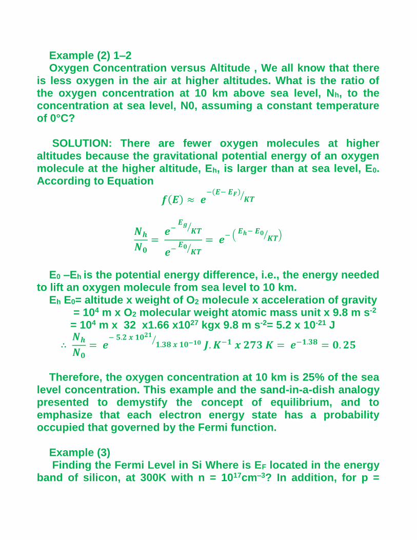
Example (2) 1–2 Oxygen Concentration versus Altitude , We all know that there
is less oxygen in the air at higher altitudes. What is the ratio of the oxygen concentration at 10 km above sea level, Nh, to the concentration at sea level, N0, assuming a constant temperature of 0°C?
SOLUTION: There are fewer oxygen molecules at higher
altitudes because the gravitational potential energy of an oxygen molecule at the higher altitude, Eh, is larger than at sea level, E0. According to Equation
𝒇(𝑬) ≈ 𝒆−(𝑬− 𝑬𝑭)
𝑲𝑻⁄
𝑵𝒉𝑵𝟎
= 𝒆−
𝑬𝒈𝑲𝑻⁄
𝒆− 𝑬𝟎
𝑲𝑻⁄= 𝒆
− ( 𝑬𝒉− 𝑬𝟎
𝑲𝑻⁄ )
E0 –Eh is the potential energy difference, i.e., the energy needed
to lift an oxygen molecule from sea level to 10 km. Eh E0= altitude x weight of O2 molecule x acceleration of gravity = 104 m x O2 molecular weight atomic mass unit x 9.8 m s-2 = 104 m x 32 x1.66 x1027 kgx 9.8 m s-2= 5.2 x 10⁻²¹ J
∴ 𝑵𝒉𝑵𝟎
= 𝒆− 𝟓.𝟐 𝒙 𝟏𝟎𝟐𝟏
𝟏.𝟑𝟖 𝒙 𝟏𝟎−𝟏𝟎⁄
𝑱. 𝑲−𝟏 𝒙 𝟐𝟕𝟑 𝑲 = 𝒆−𝟏.𝟑𝟖 = 𝟎. 𝟐𝟓
Therefore, the oxygen concentration at 10 km is 25% of the sea
level concentration. This example and the sand-in-a-dish analogy presented to demystify the concept of equilibrium, and to emphasize that each electron energy state has a probability occupied that governed by the Fermi function.
Example (3) Finding the Fermi Level in Si Where is EF located in the energy
band of silicon, at 300K with n = 1017cm–3? In addition, for p =

1014cm–3? Solution: From Eq.
𝒏 = 𝑵𝒄𝒆−(𝑬𝒄−𝑬𝑭)
𝑲𝑻⁄
𝑬𝒄 − 𝑬𝒇 = 𝑲𝑻 𝒍𝒏 (𝑵𝒄
𝒏⁄ )
= 𝟎. 𝟎𝟐𝟔 𝒍𝒏 (𝟐. 𝟖 𝒙 𝟏𝟎𝟏𝟗
𝟏𝟎𝟏𝟕⁄ ) = 𝟎. 𝟏𝟒𝟔 𝒆𝑽
Therefore, EF is located at 146 meV below Ec, as shown in Figure. For p = 1014cm–3, from Equation,
𝑬𝑭 − 𝑬𝒗 = 𝑲𝑻 𝒍𝒏 (𝑵𝒗
𝒑⁄ )
= 𝟎. 𝟎𝟐𝟔 𝒍𝒏 (𝟏. 𝟒 𝒙 𝟏𝟎𝟏𝟗
𝟏𝟎𝟏𝟒⁄ ) = 𝟎. 𝟑𝟏 𝒆𝑽
Therefore, EF is located at 0.31 eV above Ev. 0.146 Ec
EF EF 0.31 Ev
Example (1) Complete Ionization of the Dopant Atoms In a silicon sample
doped with 1017cm–3 of phosphorus atoms, what fraction of the donors are not ionized (i.e., what fraction are occupied by the “extra” electrons)?
Solution: First, assume that all the donors are ionized and each donor
donates an electron to the conduction band. N = ND = 1017 cm-3
From, previous example, EF is located at 146 meV below Ec. The donor level Ed is located at 45 meV below Ec for phosphorus (see Table).

The probability that a donor is not ionized, i.e., the probability
that it is occupied by the “extra” electron, according to Eq. 𝒇(𝑬) =
𝟏
𝟏+ 𝒆(𝑬− 𝑬𝑭)
𝑲𝑻⁄
, is :
𝑷𝒓𝒐𝒃𝒂𝒃𝒊𝒍𝒊𝒕𝒚 𝒐𝒇 𝒏𝒐𝒏 − 𝒊𝒐𝒏𝒊𝒛𝒂𝒕𝒊𝒐𝒏 ≈ 𝟏
𝟏 + 𝟏 𝟐⁄ 𝒆(𝑬𝒅−𝑬𝒇)
𝑲𝑻⁄
= 𝟏
𝟏 + 𝟏 𝟐⁄ 𝒆(𝟏𝟒𝟔−𝟒𝟓)𝒎𝒆𝑽
𝟐𝟔𝒎𝒆𝑽⁄
= 𝟑. 𝟗 %
(The factor 1/2 in the denominators stems from the complication that a donor atom can hold an electron with upspin or downspin. This increases the probability that donor state occupied by an electron.) Therefore, it is reasonable to assume complete ionization, i.e., n = Nd.
Ec 45m eV 146 m eV ED
Ef Ev
Location of EF and Ed. Not to scale.
Part (8) Solved PROBLEMS Energy: Density of States Example 2.3 Calculate the number of states per unit energy in a 100 by 100 by 10 nm piece of silicon (m* = 1.08 m0) 100 meV above the conduction band edge. Write the result in units of eV-1.

Solution The density of states equals:
𝒈(𝑬) = 𝟖 𝒑 √𝟐
𝒉𝟑𝒎∗𝟑 𝟐⁄ √𝑬 − 𝑬𝒄
= 𝟖 𝒑 √𝟐(𝟏. 𝟎𝟖 𝒙 𝟗. 𝟏𝒙 𝟏𝟎−𝟑𝟏)
𝟑𝟐⁄
(𝟔. 𝟔𝟐𝟔 𝒙 𝟏𝟎− 𝟑𝟒)𝟐√𝟎. 𝟏 𝒙 𝟏. 𝟔 𝒙 𝟏𝟎−𝟏𝟗
= 𝟏. 𝟓𝟏 𝒙 𝟏𝟎𝟓𝟔𝒎−𝟑𝑱−𝟏 So that the total number of states per unit energy equals
𝒈 (𝑬) 𝑽 = 𝟏. 𝟓𝟏 𝒙 𝟏𝟎𝟓𝟔 𝒙 𝟏𝟎−𝟐𝟐𝑱−𝟏 = 𝟐. 𝟒𝟏 𝒙 𝟏𝟎𝟓𝒆𝑽−𝟏
Example (7) Derive the density of states in the conduction band as given by Eq.
𝑵 (𝑬)𝑴𝒄
√𝟐
𝝅𝟐𝒎𝒅𝒆
𝟑𝟐⁄ (𝑬 − 𝑬𝒄)
𝟏𝟐⁄
𝒉𝟑
(Hint: The wavelength ʎ of a standing wave is related to the length of the semiconductor L by vʎ = nx where nx is an integer. The wavelength can be expressed by de Broglie hypothesis ʎ = h/px. Consider a three-dimensional cube of side L)
Example (8) 10. Calculate the average kinetic energy of electrons in the conduction band of an n-type non- degenerate semiconductor. The density of states is given by Eq.
𝑵 (𝑬)𝑴𝒄
√𝟐
𝝅𝟐𝒎𝒅𝒆
𝟑𝟐⁄ (𝑬 − 𝑬𝒄)
𝟏𝟐⁄
𝒉𝟑
Exercise (1 ) Derive the expression.

𝒑 = 𝟏
𝟒(𝟐 𝒎𝒉 𝑲𝑻
𝝅 𝒉𝟐)
𝟑𝟐⁄
𝒆(𝑬𝒗− 𝑬𝑭)
𝑲𝑻⁄ = 𝑵𝒗 𝒆(𝑬𝒗− 𝑬𝒄𝑭)
𝑲𝑻⁄
For an intrinsic semiconductor the number of electrons in the conduction band is equal to the number of holes in the valence band since a hole is left in the valence band only when an electron makes a transition to the conduction band,
n = p Using this and assuming that the effective masses of the electrons and holes are the same one gets,
𝒆(𝑬𝑭− 𝑬𝒄)
𝒌𝑻⁄ = 𝒆
(𝑬𝒗− 𝑬𝑭)𝒌𝑻⁄
Giving :
𝑬𝑭 = 𝑬𝑪 + 𝑬𝑽
𝟐 (𝑪)
i.e. the Fermi level lies in the middle of the forbidden gap. Note that there is no contradiction with the fact that no state exists in the gap as is only an energy level and not a state. By substituting the above expression for Fermi energy in(A) or (B),
𝒏 = 𝟏
𝟒(𝟐 𝒎𝒆 𝑲𝑻
𝝅 𝒉𝟐)
𝟑𝟐⁄
𝒆(𝑬𝑭− 𝑬𝑪)
𝑲𝑻⁄ = 𝑵𝑪 𝒆(𝑬𝑭− 𝑬𝒄)
𝑲𝑻⁄ (𝑨)
Conduction Band
EC Fermi Level EV
Valance Band E
ne
rgy

𝒑 = 𝟏
𝟒(𝟐 𝒎𝒉 𝑲𝑻
𝝅 𝒉𝟐)
𝟑𝟐⁄
𝒆(𝑬𝒗− 𝑬𝑭)
𝑲𝑻⁄ = 𝑵𝒗 𝒆(𝑬𝒗− 𝑬𝒄𝑭)
𝑲𝑻⁄ (𝑩)
We obtain an expression for the number density of electrons or holes (n = p = ni)
𝒏𝒊 = 𝟏
𝟒(𝟐 𝑲𝑻
𝝅 𝒉𝟐)
𝟑𝟐⁄
(𝒎𝒆𝒎𝒉)𝟑𝟒 ⁄ 𝒆
−𝚫𝟐 𝑲𝑻⁄ (𝑫)
Where Δ is the width of the gap Example 2.4 Calculate the effective densities of states in the conduction and valence bands of germanium, silicon and gallium arsenide at 300 K. Solution The effective density of states in the conduction band of germanium equals:
𝑵𝒄 = 𝟐 (𝟐 𝒑 𝒎𝒆
∗ 𝑲𝑻
𝒉𝟐)
𝟑𝟐⁄
= 𝟐 (𝟐 𝒑 𝒙 𝟎. 𝟓𝟓 𝒙 𝟗. 𝟏𝟏 𝒙 𝟏𝟎−𝟑𝟏 𝒙 𝟏. 𝟑𝟖 𝒙 𝟏𝟎−𝟐𝟐 𝒙 𝟑𝟎𝟎
(𝟔. 𝟔𝟐𝟔 𝒙 𝟏𝟎−𝟑𝟒)𝟐)
𝟑𝟐⁄
= 𝟏. 𝟎𝟐 𝒙 𝟏𝟎𝟐𝟓𝒎−𝟑 = 𝟏. 𝟎𝟐 𝒙 𝟏𝟎𝟏𝟗𝒄𝒎−𝟑 where the effective mass for density of states was. Similarly, one finds the effective density of states in the conduction band for other semiconductors and the effective density of states in the valence band:
Germanium Silicon Gallium Arsenide
Nc (cm-3) 1.02 x 10¹⁹ 2.81 x 10¹⁹ 4.35 x 10¹⁷
Nv (cm-3) 5.64 x 10¹⁸ 1.83 x 10¹⁹ 7.57 x 10¹⁸
Note that the effective density of states is temperature dependent and can be obtain from:

𝑵𝒄(𝑻) = 𝑵𝒄(𝟑𝟎𝟎𝑲) (𝑻
𝟑𝟎𝟎)
𝟑𝟐⁄
where Nc(300 K) is the effective density of states at 300 K.
Part (9) Solved PROBLEMS Compounds
Problem (1) Consider the GaAs crystal at 300 K. a. Calculate the intrinsic conductivity and resistivity. b. In a sample containing only 1015 cm-3 ionized donors, where is the Fermi level? What is the conductivity of the sample? c. In a sample containing 1015 cm-3 ionized donors and 9 × 1014 cm-3 ionized acceptors, what is the free hole concentration? Solution: a - Given temperature, T = 300 K, and intrinsic GaAs. From Tables,
ni = 1.8 × 106 cm-3, µe ≈ 8500 cm2 V-1 s-1 and µh ≈ 400 cm2 V-1 s-1. Thus, σ = eni( µe + µh) ∴σ = (1.602 × 10⁻¹⁹ C)(1.8 × 106 cm-3)(8500 cm2 V-1 s-1 + 400 cm2 V-1 s-1) ∴σ = 2.57 × 10⁻⁹Ω-1 cm-1 ∴ρ = 1/ σ = 3.89 × 10⁸Ω cm B - Donors are now introduced. At room temperature, n = Nd = 1015 cm-3>>ni>> p. σ n = eNdµe≈(1.602 ×10⁻¹⁹ C)(1015 cm-3)(8500 cm2 V-1 s-1) = 1.36 Ω-1 cm-
1∴ρn = 1/ σn = 0.735 Ω cm In the intrinsic sample, EF = EFi, ni = Ncexp[−(Ec − EFi)/kT] ( 1 ) In the doped sample,

n = Nd, EF = E=, n = Nd = Ncexp[−(Ec − EFn)/kT] (2) Eqn. (2) divided by Eqn. (1) gives, Nd/ni = exp (EFn − EFi)/ kT ( 3 ) ∴∆EF = EFn − EFi = kT ln(Nd/ni) (4) Substituting we find, ∆EF = (8.617 × 10⁻⁵ eV/K)(300 K)ln[(1015 cm-3)/(1.8 × 106 cm-3)] ∴∆EF = 0.521 eV above EFi (intrinsic Fermi level) c The sample is further doped with Na = 9 × 1014 cm-3 = 0.9 × 1015 cm-3 acceptors. Due to compensation, the net effect is still an n-type semiconductor but with an electron concentration given by, n = Nd − Na = 1015 cm-3 − 0.9 × 1015 cm-3 = 1 × 1014 cm-3 (>>ni) The sample is still n-type though there are less electrons than before due to the compensation effect. From the mass action law, the hole concentration is: p = ni
2 / n = (1.8 × 106 cm-3)2 / (1 × 1014 cm-3) = 0.0324 cm-3 On average there are virtually no holes in 1 cm3 of sample. We can also calculate the new conductivity. We note that electron scattering now occurs from Na + Nd number of ionized centers though we will assume that µe ≈ 8500 cm2 V-1 s-1. σ = en µe≈ (1.602 × 10⁻¹⁹ C)(1014 cm-3)(8500 cm2 V-1 s-1) = 0.136 Ω-1 cm-1
Problem (2) AlN and GaSb are compounds, solid at room temperature. On the basis of bonding considerations and data provided in the periodic table, attempt to predict differences in the properties of these solids. Solution Both compounds are of the III–V family, which hybridize and form “adamantine” (diamond–like) structures which places them into the category of semiconductor. AlN ΔEN = 1.43. The covalent radii of the constituents are small and, combined with the large EN, the bonds (polar covalence’s) are very strong – the semiconductor is expected to exhibit a large band gap (likely transparent). GaSb ΔEN = 0.24. The covalent radii of both constituents are significantly larger (than those of AlN), the ionic contribution to bonding is small – the semiconductor is expected to exhibit a much smaller band gap than AlN. AlN: Eg = 3.8 eV ,GaSb: Eg = 0.8 eV

Problem (4) Calculate thermal velocity of electrons and holes in GaAs at room temperature. Effective masses are m∗
e/m0 = 0.063 and m∗h/m0 = 0.53.
Solution:
𝒗𝒕 = ∫ 𝒗 𝒆𝒙𝒑 (− 𝒎
∗𝒗𝟐𝟐𝑲𝑻⁄ )𝒅𝟑 𝒗
∞
𝟎
∫ 𝒆𝒙𝒑 (− 𝒎∗𝒗𝟐
𝟐𝑲𝑻⁄ )𝒅𝟑 𝒗∞
𝟎
= √𝟖𝑲𝑻
𝝅 𝒎∗
Thermal velocities of electrons and holes are 4.3×10⁷ and 1.5×107 cm/s, respectively.
Part (10) Solved PROBLEMS
Transparent Semiconductors 1. Which of the following semiconductors are transparent, partially transparent, nontransparent for visible light (λ = 0.4 – 0.7 μm): Si, GaAs, GaP, and GaN? Solution: (1.1) 1. It follows from Table 2 that Si and GaAs are not transparent, GaP is partially transparent, and GaN is transparent for the visible light. Problem (3) 1. Which of the following semiconductors are transparent, partially transparent, non transparent for visible light (λ = 0.4–0.7 µm): Si, GaAs, GaP, and GaN? Solution: 1. It follows from Table 2 that Si and GaAs are not transparent, GaP is partially transparent, and GaN is transparent for the visible light.

Example (1) Measuring the Band-Gap Energy if a semiconductor is transparent to light with a wavelength longer than 0.87 µm, what is its band-gap energy?
SOLUTION: Photon energy of light with 0.87 µm wavelength is,
with c being the speed of light
𝒉 𝒗 = 𝒉 𝒄
𝝀= 𝟔. 𝟔𝟑 𝒙 𝟏𝟎−𝟑𝟒(𝒋. 𝒔) 𝒙 𝟑 𝒙 𝟏𝟎𝟖 𝒎/𝒔
𝟎. 𝟖𝟕 𝝁𝒎
= 𝟏. 𝟗𝟗 𝒙 𝟏𝟎−𝟏𝟗 𝒋 𝝁𝒎
𝒐. 𝟖𝟕 𝝁𝒎
= 𝟏. 𝟗𝟗 𝒙 𝟏𝟎−𝟏𝟗 𝒆𝑽 𝝁𝒎
𝟏. 𝟔 𝒙 𝟏𝟎−𝟏𝟗 𝒙 𝒐. 𝟖𝟕 𝝁𝒎
= 𝟏. 𝟐𝟒 𝒆𝑽 𝝁𝒎
𝒐. 𝟖𝟕 𝝁𝒎= 𝟏. 𝟒𝟐 𝒆𝑽
Therefore, the band gap of the semiconductor is 1.42 eV. The
semiconductor is perhaps GaAs (Table). Band-gap energies of selected semiconductors.
Semiconductor InSb Ge Si GaAs GaP ZnSe Diamond
Eg (eV) 0.18 0.67 1.12 1.42 2.25 2.7 6.0
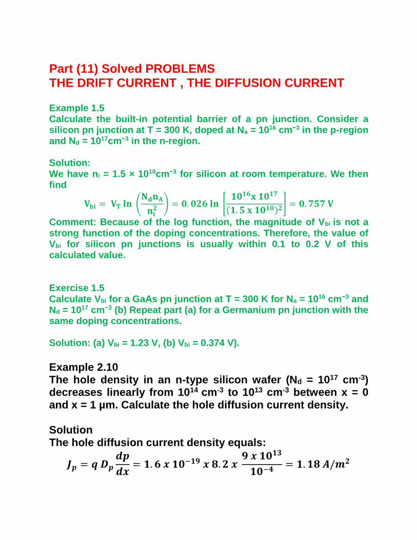
Part (11) Solved PROBLEMS THE DRIFT CURRENT , THE DIFFUSION CURRENT Example 1.5 Calculate the built-in potential barrier of a pn junction. Consider a silicon pn junction at T = 300 K, doped at Na = 1016 cm−3 in the p-region and Nd = 1017cm−3 in the n-region. Solution: We have ni = 1.5 × 1010cm−3 for silicon at room temperature. We then find
𝐕𝐛𝐢 = 𝐕𝐓 𝐥𝐧 (𝐍𝐝𝐧𝐀
𝐧𝐢𝟐 ) = 𝟎. 𝟎𝟐𝟔 𝐥𝐧 [
𝟏𝟎𝟏𝟔𝐱 𝟏𝟎𝟏𝟕
(𝟏. 𝟓 𝐱 𝟏𝟎𝟏𝟎)𝟐] = 𝟎. 𝟕𝟓𝟕 𝐕
Comment: Because of the log function, the magnitude of Vbi is not a strong function of the doping concentrations. Therefore, the value of Vbi for silicon pn junctions is usually within 0.1 to 0.2 V of this calculated value. Exercise 1.5 Calculate Vbi for a GaAs pn junction at T = 300 K for Na = 1016 cm−3 and Nd = 1017 cm−3 (b) Repeat part (a) for a Germanium pn junction with the same doping concentrations.
Solution: (a) Vbi = 1.23 V, (b) Vbi = 0.374 V).
Example 2.10 The hole density in an n-type silicon wafer (Nd = 1017 cm-3) decreases linearly from 1014 cm-3 to 1013 cm-3 between x = 0 and x = 1 µm. Calculate the hole diffusion current density. Solution The hole diffusion current density equals:
𝑱𝒑 = 𝒒 𝑫𝒑𝒅𝒑
𝒅𝒙= 𝟏. 𝟔 𝒙 𝟏𝟎−𝟏𝟗 𝒙 𝟖. 𝟐 𝒙
𝟗 𝒙 𝟏𝟎𝟏𝟑
𝟏𝟎−𝟒= 𝟏. 𝟏𝟖 𝑨/𝒎𝟐

𝑫𝒑 = 𝑽𝒕𝒎𝒑 = 𝟎. 𝟎𝟐𝟓𝟗 𝒙 𝟑𝟏𝟕 = 𝟖. 𝟐 𝒎𝟐
𝒔⁄
and the hole mobility in the n-type wafer was obtained from Table as the hole mobility in a p-type material with the same doping density. Problem 2.18 Consider the problem of finding the doping density, which results in the maximum possible resistivity of silicon at room temperature. (ni = 1010 cm-3, µn = 1400 cm2/V-sec and µp = 450 cm2/V-sec.) Should the silicon be doped at all or do you expect the maximum resistivity when dopants are added? If the silicon should be doped, should it be doped with acceptors or donors (assume that all dopant is shallow). Calculate the maximum resistivity, the corresponding electron and hole density and the doping density. Solution Since the mobility of electrons is larger than that of holes, one expects the resistivity to initially decrease as acceptors are added to intrinsic silicon. The maximum resistivity (or minimum conductivity) is obtained from:
𝒅𝒔
𝒅𝒏= 𝒒
𝒅 (𝒏 𝝁𝒏 + 𝒑 𝝁𝒑)
𝒅𝒏= 𝒒
𝒅 (𝒏 𝝁𝒏 +𝒏𝒊𝟐
𝒏𝝁𝒑)
𝒅𝒏= 𝟎
which yields:
𝒏 = √𝝁𝒑
𝝁𝒏𝒏𝒊 = 𝟎. 𝟓𝟕 𝒏𝒊 = 𝟓. 𝟕 𝒙 𝟏𝟎𝟗𝒄𝒎−𝟑
The corresponding hole density equals p = 1.76 ni = 1.76 x 109 cm-3 and the amount of acceptors one needs to add equals Na = 1.20 ni = 1.20 x 109 cm-3. The maximum resistivity equals:
𝝆𝒎𝒂𝒙 = 𝟏
𝒒 (𝒏 𝝁𝒏 + 𝒑 𝝁𝒑)=
𝟏
𝒒 𝒏𝒊 𝒙 𝟏𝟓𝟖𝟕= 𝟑𝟗𝟒 𝑲𝛀 𝒄𝒎

Problem 2.30 Phosphorous donor atoms with a concentration of 1016 cm-3 are added to a piece of silicon. Assume that the phosphorous atoms are distributed homogeneously throughout the silicon. The atomic weight of phosphorous is 31. a) What is the sample resistivity at 300 K? b) What proportion by weight does the donor impurity comprise? The density of silicon is 2.33 gram/cm3. c) If 1017 atoms cm-3 of boron are included in addition to phosphorous, and distributed uniformly, what is the resulting resistivity and type (i.e., p- or n-type material)? d) Sketch the energy-band diagram under the condition of
part c) and show the position of the Fermi energy relative to the valence band edge.
Solution a) The electron mobility in the silicon equals
𝝁𝒏 = 𝝁𝒎𝒂𝒙 + 𝝁𝒎𝒂𝒙 − 𝝁𝒎𝒊𝒏
𝟏 + (𝑵𝑫
𝑵𝝆)𝒂 = 𝟔𝟖. 𝟓 +
𝟏𝟒𝟏𝟒 − 𝟔𝟖. 𝟓
𝟏 + (𝟏𝟎𝟏𝟔
𝟗.𝟐 𝒙 𝟏𝟎𝟏𝟔)𝟎.𝟕𝟏𝟏
= 𝟏𝟏𝟖𝟒 𝒄𝒎𝟐/𝒗𝒔
𝝆 = 𝟏
𝒔=
𝟏
𝒒 (𝒏 𝝁𝒏 + 𝒑 𝝁𝒑)=
𝟏
𝟏. 𝟔 𝒙 𝟏𝟎−𝟏𝟗 𝒙 𝟏𝟏𝟖𝟒𝒙 𝟏𝟎𝟏𝟔
= 𝟎. 𝟓𝟑 𝛀 𝒄𝒎 b)

𝒘𝒆𝒊𝒈𝒉𝒕
𝒗𝒐𝒍𝒖𝒎𝒆|𝒑
𝒘𝒆𝒊𝒈𝒉𝒕
𝒗𝒐𝒍𝒖𝒎𝒆|𝒑+𝒔𝒊
|=
𝑴𝒎 𝑨 𝑵𝒅𝒅𝒆𝒏𝒔𝒊𝒕𝒚 𝒐𝒇 𝒔𝒊
= 𝟑𝟏 𝒙 𝟏. 𝟔 𝒙 𝟏𝟎𝟐𝟕 𝒙 𝟏𝟎𝟑 𝒙 𝟏𝟎𝟏𝟔
𝟐𝟗𝟐𝟖
= 𝟐. 𝟏 𝒙 𝟏𝟎−𝟕 c) The semiconductor is p-type since Na>Nd The hole density is obtained from:
𝒑 = 𝑵𝒂+ − 𝑵𝒅
−
𝟐+ √(
𝑵𝒂+ − 𝑵𝒅
−
𝟐)
𝟐
+ 𝒏𝒊𝟐
= 𝟗 𝒙 𝟏𝟎𝟏𝟔
𝟐+ √(
𝟗 𝒙 𝟏𝟎𝟏𝟔
𝟐)
𝟐
+ (𝟏𝟎𝟏𝟎)𝟐 = 𝟗 𝒙 𝟏𝟎𝟏𝟔𝒄𝒎−𝟑
and the mobility is calculated from the sum of the donor and acceptor densities
𝝁𝒑 = 𝝁𝒎𝒊𝒏 + 𝝁𝒎𝒂𝒙 − 𝝁𝒎𝒊𝒏
𝟏 + (𝑵
𝑵𝝆)𝒂 = 𝟒𝟒. 𝟗 +
𝟒𝟕𝟎. 𝟓 − 𝟒𝟒. 𝟗
𝟏 + (𝟏𝟏𝒙 𝟏𝟎𝟏𝟔
𝟐.𝟐𝟑 𝒙 𝟏𝟎𝟏𝟕)𝟎.𝟕𝟏𝟏
= 𝟑𝟏𝟎. 𝟔 𝒄𝒎𝟐/𝒗𝒔 leading to the conductivity of the material:
𝝆 = 𝟏
𝒔=
𝟏
𝒒 (𝒏 𝝁𝒏 + 𝒑 𝝁𝒑)=
𝟏
𝟏. 𝟔 𝒙 𝟏𝟎−𝟏𝟗 𝒙 𝟑𝟏𝟎. 𝟔𝒙 𝟗𝒙 𝟏𝟎𝟏𝟔
= 𝟎. 𝟐𝟐 𝛀 𝒄𝒎 d)
𝑬𝑭 − 𝑬𝒗 = 𝑲𝑻 𝒍𝒏 𝑵𝒗𝒑= 𝟎. 𝟎𝟐𝟓𝟗 𝒍𝒏
𝟏𝟎𝟏𝟒
𝟗 𝒙 𝟏𝟎𝟏𝟔= 𝟏𝟐𝟑 𝒎𝒆𝑽
Problem 2.32 The electron concentration in a piece of lightly doped, n-type silicon at room temperature varies linearly from 1017 cm-3 at x = 0 to 6 x 1016 cm-3 at x = 2 µm. Electrons are supplied to keep this concentration constant with time. Calculate the electron current density in the silicon if no electric field is present.

Assume µn = 1000 cm2/V-s and T = 300 K. Solution The diffusion current is obtained from:
𝑱𝒏 = 𝒒 𝑫𝒏𝒅𝒏
𝒅𝒙= 𝟏. 𝟔 𝒙 𝟏𝟎−𝟏𝟗 𝒙 𝟐𝟓. 𝟖 𝒙
𝟏𝟎−𝟏𝟕 − 𝟔 𝒙 𝟏𝟎𝟏𝟔
𝟐 𝒙 𝟏𝟎−𝟒
= 𝟖𝟐𝟖 𝑨/𝒎𝟐 where the diffusion constant Dn is obtained from:
Dn = µn x Vt = 1000 x 0.0258 = 25.8 cm2 Example 4.1 An abrupt silicon p-n junction consists of a p-type region containing 2 x 1016 cm-3 acceptors and an n-type region containing also 1016 cm-3 acceptors in addition to 1017 cm-3 donors. a. Calculate the thermal equilibrium density of electrons and holes in the p-type region as well as both densities in the n-type region. b. Calculate the built-in potential of the p-n junction. c. Calculate the built-in potential of the p-n junction at 400 K. Solution a. The thermal equilibrium densities are: In the p-type region:
𝒑 = 𝑵𝒂 = 𝟐 𝒙 𝟏𝟎𝟏𝟔𝒄𝒎−𝟑 , 𝒏 =
𝒏𝒊𝟐
𝒑=
𝟏𝟎𝟐𝟎
𝟐 𝒙 𝟏𝟎𝟏𝟔= 𝟓 𝒙 𝟏𝟎𝟑𝒄𝒎−𝟑
In the n-type region
𝒏 = 𝑵𝒅 − 𝑵𝒂 = 𝟗 𝒙 𝟏𝟎𝟏𝟔𝒄𝒎−𝟑 , 𝒑 = 𝒏𝒊𝟐
𝒏=
𝟏𝟎𝟐𝟎
𝟏 𝒙 𝟏𝟎𝟏𝟔
= 𝟏. 𝟏𝟏 𝒙 𝟏𝟎𝟑𝒄𝒎−𝟑 b. The built-in potential is obtained from
𝒇𝒊 = 𝑽𝒕 𝒍𝒏 𝒑𝒑𝒏𝒏
𝒏𝒊𝟐 = 𝟎. 𝟎𝟐𝟓𝟗 𝒍𝒏
𝟐 𝒙 𝟏𝟎𝟏𝟔 𝒙 𝟗 𝒙 𝟏𝟎𝟏𝟔
𝟏𝟎𝟐𝟎= 𝟎. 𝟕𝟗𝑽
c. Similarly, the built-in potential at 400 K equals

𝒇𝒊 = 𝑽𝒕 𝒍𝒏 𝒑𝒑𝒏𝒏
𝒏𝒊𝟐 = 𝟎. 𝟎𝟑𝟒𝟓 𝒍𝒏
𝟐 𝒙 𝟏𝟎𝟏𝟔 𝒙 𝟗 𝒙 𝟏𝟎𝟏𝟔
(𝟒. 𝟓𝟐 𝒙𝟏𝟎𝟏𝟐)𝟐= 𝟎. 𝟔𝟑𝑽
where the intrinsic carrier density at 400 K was obtained from Example 2.4 b. Example 1.4 Calculate the diffusion current density for a given semiconductor. Consider silicon at T = 300 K. Assume the electron concentration varies linearly from n = 1012 cm−3 to n = 1016 cm−3 over the distance from x = 0 to x = 3 μm. Assume Dn = 35 cm2/s. We have
𝐉 = 𝐞 𝐃𝐧 𝐝𝐧
𝐝𝐱= 𝐞 𝐃𝐧
𝚫 𝐧
𝚫 𝐱= 𝟏 . 𝟔 𝐱 𝟏𝟎−𝟏𝟗 𝐱 𝟑𝟓 𝐱 (
𝟏𝟎𝟏𝟐 − 𝟏𝟎𝟏𝟔
𝟎 − 𝟑 𝐱 𝟏𝟎−𝟒) = 𝟏𝟖𝟕 𝐀
𝐦𝟐⁄
Comment: Diffusion current densities on the order of a few hundred amperes per square centimeter can also be generated in a semiconductor. Exercise 1.4 Consider silicon at T = 300 K. Assume the hole concentration is given by p = 1016e−x/Lp (cm−3), where Lp = 10−3 cm. Calculate the hole diffusion current density at (a) x = 0 and (b) x = 10−3cm. Assume Dp = 10 cm2/s. Solution: (a) 16 A/cm2, (b) 5.89 A/cm2) Example 1.7 Determine the current in a pn junction diode. Consider a pn junction at T = 300 K in which IS = 10−14 A and n = 1. Find the diode current for VD = +0.70 V and VD = −0.70 V. Solution: For VD = +0.70 V, the pn junction is forward-biased and we find
𝐢𝐃 = 𝐈𝐬 [𝐞𝐕𝐃
𝐕𝐓⁄
− 𝟏] = 𝟏𝟎−𝟏𝟒 [𝐞𝟎.𝟕
𝟎,𝟎𝟐𝟔⁄ − 𝟏] ⟶ 𝟒. 𝟗𝟑 𝐦𝐀
For 𝛖𝐃 = −𝟎. 𝟕 𝐕 , the pn junction is reverse bias

𝐢𝐃 = 𝐈𝐬 [𝐞𝐕𝐃
𝐕𝐓⁄
− 𝟏] = 𝟏𝟎−𝟏𝟒 [𝐞−𝟎.𝟕
𝟎,𝟎𝟐𝟔⁄ − 𝟏] ≅ − 𝟏𝟎−𝟏𝟒 𝐀
Comment: Although IS is quite small, even a relatively small value of forward-bias voltage can induce a moderate junction current. With a reverse-bias voltage applied, the junction current is virtually zero. Exercise 1.7 (a) A silicon pn junction at T = 300 K has a reverse-saturation current of IS = 2 × 10⁻¹⁴ A. Determine the required forward-bias voltage to produce a current of (i) ID = 50 μA and (ii) ID = 1 mA. (b) Repeat part (a) for IS = 2 × 10⁻¹² Solution a. (i) 0.563 V, (ii) 0.641 V; (b) (i) 0.443 V, (ii) 0.521 V).
Part (12) Solved PROBLEMS continuity equation
Problem (1) Consider n-type silicon with Nd = 1015cm−3 at T = 300K. A light source is turned on at t = 0. The source illuminates the semiconductor uniformly, generating carriers at the rate of Gn = Gp = 1019cm−3s−1. There is no applied field. (a) Write down the continuity equation and solve it to find the expression for the excess minority carrier concentration,
𝜹𝒑(𝒕), as a function of time for t ≥ 0. Solution: When there is no applied electric field the carrier distribution is diffusion driven. The continuity equation for the minority carrier
𝝏𝒑(𝒙 , 𝒕)
𝝏𝒕= 𝟏
𝒒
𝝏 𝑱𝒑 (𝒙 , 𝒕)
𝝏𝒙+ 𝑮𝒑(𝒙 , 𝒕) − 𝑹𝒑(𝒙 , 𝒕)
Then reduces to ,

𝝏𝜹𝒑
𝝏𝒕= 𝑮𝒑 −
𝝏𝜹𝒑
𝝉𝒑
With the general solution
𝜹𝒑(𝒕) = 𝑨 𝒆𝒙𝒑 (− 𝒕
𝝅𝒑) + 𝑮𝒑𝝉𝒑
Using the initial condition (before the light was turned on)
that 𝜹𝒑(𝒕) = 0, then we find that𝑨 = − 𝑮𝒑𝝉. The full solution
then is,
𝜹𝒑(𝒕) = 𝑮𝒑𝝉𝒑 𝟏 − 𝒆𝒙𝒑 (− 𝒕
𝝉𝒑)
(b) As t →∞, the system will approach steady state. When the steady state excess carrier concentration is 5×1013cm−3, find
the minority carrier lifetime, 𝝉𝒑.
Solution: The system will approach steady state as t → ∞. Evidently, the steady state carrier density is given
𝜹𝒑(𝒕)|𝐭 → ∞ = 𝑮𝒑𝝉𝒑. The 𝝉𝒑 must then take on the value
𝝉𝒑 =𝟓 𝒙 𝟏𝟎𝟏𝟑
𝑮𝒑⁄ . With Gp = 1019 cm−3s−1, then the minority
(hole) carried lifetime must be 𝝉𝒑 = 5×10⁻⁶s.
(c) Determine the time at which the excess carrier concentration becomes half of the steady state
value,𝜹𝒑(𝒕)|𝐭 → ∞ that you calculated in (b). Solution: The value at which
𝒆𝒙𝒑 (− 𝒕
𝝉) =
𝟏
𝟐 𝒔𝒐, 𝒕 = 𝒍𝒏 (𝟐)𝝉𝒑 = 𝟎. 𝟔𝟗 𝒙 𝟓 𝒙 𝟏𝟎−𝟔 𝒔
Problem (2) 2. Consider an n-type semiconductor as shown. Illumination

produces a constant excess carrier generation rate of Gp is the region −L ≤ x ≤ L. Assume the minority current density is zero at x = −3L and x = 3L. Find the steady state minority
carrier concentration as a function of x, 𝜹𝒑(𝒙). There is no applied electric field. Solution: When there is no applied electric field the carrier distribution is diffusion driven. The continuity equation for the minority carrier
𝝏𝒑(𝒙 , 𝒕)
𝝏𝒕= 𝟏
𝒒
𝝏 𝑱𝒑 (𝒙 , 𝒕)
𝝏𝒙+ 𝑮𝒑(𝒙 , 𝒕) − 𝑹𝒑(𝒙 , 𝒕)
Then reduces to,
𝟎 = 𝑫𝒑𝝏𝟐𝜹𝒑(𝒙, 𝒕)
𝝏𝟐+ 𝑮𝒑 −
𝜹𝒑
𝝉𝒑
In − 𝑳 ≤ 𝒙 ≤≤ 𝑳 And
𝟎 = 𝑫𝒑𝝏𝟐𝜹𝒑(𝒙, 𝒕)
𝝏𝟐 −
𝜹𝒑
𝝉𝒑
In − 𝟑𝑳 ≤ 𝒙 ≤≤ −𝑳 𝒂𝒏𝒅 𝑳 ≤ 𝒙 ≤≤ 𝟑𝑳 , with boundary conditions that
𝝏 𝜹𝒑
𝝏𝒙(− 𝟑𝑳) =
𝝏 𝜹𝒑
𝝏𝒙(𝟑 𝑳) = 𝟎
-3L -L 0 L 3L X
An illuminated semiconductor

and 𝜹𝒑(−𝑳) and 𝜹𝒑(𝑳) are continuous. From symmetry, we need only solve for x > 0 with new boundary condition that
𝝏 𝜹𝒑
𝝏𝒙(𝟎) = 𝟎
The solution is
𝜹𝒑(𝒙) =
𝑮𝒑𝝉𝒑 + 𝑨 𝒆𝒙𝒑 (−
𝒙
𝑳𝒑) + 𝑩 𝒆𝒙𝒑 (
𝒙
𝑳𝒑) 𝟎 ≤ 𝒙 ≤ 𝑳
𝑪 𝒆𝒙𝒑 (− 𝒙
𝑳𝒑) + 𝑫 𝒆𝒙𝒑 (
𝒙
𝑳𝒑) 𝑳 ≤ 𝒙 ≤ 𝟑𝑳
Where,
𝑳𝒑𝟐 = 𝑫𝒑𝝉𝒑
The end conditions at 0 and L then lead to A = B
And 𝑪 = 𝑫 𝒆𝒙𝒑 (𝟔 𝑳
𝑳𝒑)
These results in
𝜹𝒑(𝒙) =
𝑮𝒑𝝉𝒑 + 𝑬 𝒄𝒐𝒔𝒉 (
𝒙
𝑳𝒑) 𝟎 ≤ 𝒙 ≤ 𝑳
𝑭𝒄𝒐𝒔𝒉 (𝒙 − 𝟑𝑳
𝑳𝒑) 𝑳 ≤ 𝒙 ≤ 𝟑𝑳
Where
𝐄 = 𝟐𝐀 𝐚𝐧𝐝 𝐅 = 𝟐 𝐃 𝐞𝐱𝐩 (𝟑 𝑳
𝑳𝒑)
Are the new constants to find and where
𝟐 𝒄𝒐𝒔𝒉 (𝒙) = 𝒆𝒙𝒑(𝒙) + 𝒆𝒙𝒑 (−𝒙) is the hyperbolic cosine function? We will later also use the derivative of this function.
𝟐 𝒔𝒊𝒏𝒉 (𝒙) = 𝒆𝒙𝒑(𝒙) + 𝒆𝒙𝒑 (−𝒙) The hyperbolic sine function. At x = L, we find
𝑮𝒑𝝉𝒑 + 𝑬 𝒄𝒐𝒔𝒉 (𝑳
𝑳𝒑) = 𝑭 𝒄𝒐𝒔𝒉 (
𝟐𝑳
𝑳𝒑)
𝑬 𝒔𝒊𝒏𝒉 (𝒙
𝑳𝒑) = − 𝑭 𝒔𝒊𝒏𝒉 (
𝟐𝑳
𝑳𝒑)

where we have used the evenness of cosh and oddness of sinh. Solving, we find
𝑭 = − 𝒔𝒊𝒏𝒉 (
𝑳
𝑳𝒑)
𝒔𝒊𝒏𝒉 (𝟐𝑳
𝑳𝒑) 𝑬
𝑬 = − 𝑮𝒑𝝉𝒑 (
𝟐𝑳
𝑳𝒑)
𝒄𝒐𝒔𝒉 (𝑳
𝑳𝒑) 𝒔𝒊𝒏𝒉 (
𝟐𝑳
𝑳𝒑) + 𝒄𝒐𝒔𝒉 (
𝟐𝑳
𝑳𝒑) 𝒔𝒊𝒏𝒉 (
𝑳
𝑳𝒑)
= 𝑮𝒑𝝉𝒑𝒔𝒊𝒏𝒉 (
𝟐𝑳
𝑳𝒑)
𝒔𝒊𝒏𝒉 (𝟑𝑳
𝑳𝒑)
Where the identity,
𝒔𝒊𝒏𝒉 (𝟑𝑳
𝑳𝒑) = 𝒄𝒐𝒔𝒉 (
𝑳
𝑳𝒑) 𝒔𝒊𝒏𝒉 (
𝟐𝑳
𝑳𝒑) + 𝒄𝒐𝒔𝒉 (
𝟐𝑳
𝑳𝒑) 𝒔𝒊𝒏𝒉 (
𝑳
𝑳𝒑)
has been used. Substituting back, we find
𝑭 = 𝑮𝒑𝝉𝒑𝒔𝒊𝒏𝒉 (
𝑳
𝑳𝒑)
𝒔𝒊𝒏𝒉 (𝟑𝑳
𝑳𝒑)
𝜹𝒑(𝒙) = (𝟏 − 𝒔𝒊𝒏𝒉 (
𝟐𝑳
𝑳𝒑) 𝒄𝒐𝒔𝒉 (
𝒙
𝑳𝒑)
𝒔𝒊𝒏𝒉 (𝟑𝑳
𝑳𝒑)
) 𝟎 ≤ 𝒙 ≤ 𝑳
𝑮𝒑𝝉𝒑𝒔𝒊𝒏𝒉 (𝑳
𝑳𝒑) 𝒄𝒐𝒔𝒉 (
𝒙−𝟑𝑳
𝑳𝒑)
𝒔𝒊𝒏𝒉 (𝟑𝑳
𝑳𝒑)
𝑳 ≤ 𝒙 ≤ 𝟑𝑳
(b) Suppose the excess carriers are generated such that the

excess carrier concentrations are 10% of the equilibrium majority carrier concentrations. Calculate the quasi-Fermi levels relative the intrinsic Fermi levels, that is, Fn −Ei and Ei−Fp. Solution: Here we can use that
𝒏𝒐 + 𝜹𝒏 = 𝒏𝒊 𝒆𝒙𝒑 (𝑬𝒏− 𝑬𝒊
𝑲𝑻) , to find,
𝑭𝒏 − 𝑬𝒊 = 𝑲𝑻 𝒍𝒏 (𝟏. 𝟏 𝒙 𝑵𝒅
𝒏𝒊) = 𝟎. 𝟓𝟐𝟏 𝒆𝑽
The minority carriers than are given by
𝒑𝒐 = 𝒏𝒊𝟐
𝒏𝒐= 𝟒 𝒙 𝟏𝟎−𝟑𝒄𝒎−𝟑 , And ,
𝒑 = 𝒑 + 𝜹𝒑 ≈ 𝜹𝒑 = 𝒏𝒊 𝒆𝒙𝒑 (𝑬𝒊 − 𝑬𝑭𝑲𝑻
)
That yields,
𝑬𝒊 − 𝑬𝒑 = 𝑲𝑻 𝒍𝒏 (𝟎. 𝟏 𝒙 𝑵𝒅
𝒏𝒊) = 𝟎. 𝟒𝟓𝟗 𝒆𝑽
Part (13) Solved PROBLEMS PN junction theory
Example A silicon diode at temperature T = 300K has doping concentration NA = ND = 1.2x1016 cm -3 , ni = 1.5 x1010 cm -3, Dn = 25 cm2 s -1, Dp = 10 cm2 s -1, KS = 11.7, Lp = 2.2x10⁻³cm and Ln = 3.5x10⁻³cm, and cross section area = 1x10⁻² cm2 . Solution: The minority hole in n - region
𝐩𝐧𝐨 = 𝐧𝐢𝟐
𝐍𝐀= 𝟐. 𝟐𝟓𝐱𝟏𝟎𝟐𝟎
𝟏. 𝟐𝐱𝟏𝟎𝟏𝟔= 𝟏. 𝟖𝟕𝟓𝐱𝟏𝟎𝟒 𝐜𝐦−𝟑
The minority electron in npo p-region

𝐧𝐩𝐨 = 𝐧𝐢𝟐
𝐍𝐃= 𝟐. 𝟐𝟓𝐱𝟏𝟎𝟐𝟎
𝟏. 𝟐𝐱𝟏𝟎𝟏𝟔= 𝟏. 𝟖𝟕𝟓𝐱𝟏𝟎𝟒 𝐜𝐦−𝟑
The reverse saturation current
Is =𝑨 [𝒒 𝑫𝒑𝒑𝒏𝒐
𝑳𝒑+
𝒒 𝑫𝒏𝒏𝒑𝒐
𝑳𝒏] = 𝟏. 𝟔𝟎𝟐 𝒙 𝟏𝟎−𝟏𝟗 [
𝟏𝟎 𝒙 𝟏.𝟎𝟖𝟕𝟓 𝒙 𝟏𝟎𝟒
𝟐.𝟐 𝒙 𝟏𝟎−𝟑+
𝟐𝟓 𝒙 𝟏.𝟖𝟕𝟓 𝒙 𝟏𝟎𝟒
𝟑.𝟓 𝒙 𝟏𝟎−𝟑] = 𝟑. 𝟓𝟏 𝒙 𝟏𝟎−𝟏𝟑 𝑨
Example An abrupt silicon (nI = 1010 cm-3) p-n junction consists of a p-type region containing 1016 cm-3acceptors and an n-type region containing 5 x 1016 cm-3 donors.
a. Calculate the built-in potential of this p-n junction. b. Calculate the total width of the depletion region if the applied
voltage Va equals 0, 0.5 and -2.5 V. c. Calculate maximum electric field in the depletion region at 0, 0.5
and -2.5 V. d. Calculate the potential across the depletion region in the n-type
semiconductor at 0, 0.5 and -2.5 V. Solution: The built-in potential is calculated from:
The depletion layer width is obtained from:
the electric field from
and the potential across the n-type region equals

Where
One can also show that:
This yields the following numeric values:
Example: Consider an abrupt p-n diode with Na = 1018 cm-3 and Nd = 1016 cm-3. Calculate the junction capacitance at zero bias. The diode area equals 10-4 cm2. Repeat the problem while treating the diode as a one-sided diode and calculate the relative error.
Solution: The built in potential of the diode equals:
The depletion layer width at zero bias equals:
And the junction capacitance at zero bias equals:

Repeating the analysis while treating the diode as a one-sided diode, one only has to consider the region with the lower doping density so that
And the junction capacitance at zero bias equals
The relative error equals 0.5 %, which justifies the use of the one-sided approximation. Example
An abrupt silicon p-n junction (Na = 1016 cm-3 and Nd = 4 x 1016 cm-3) is biased with Va = 0.6 V. Calculate the ideal diode current assuming that the n-type region is much smaller than the diffusion length with wn
' = 1 mm and assuming a "long" p-type region. Use mn = 1000 cm2/V-s and mp = 300 cm2/V-s. The minority carrier lifetime is 10 ms and the diode area is 100 mm by 100 mm. Solution: The current is calculated from:
With Dn = mn Vt = 1000 x 0.0258 = 25.8 cm2/V-s Dp = mp Vt = 300 x 0.0258 = 7.75 cm2/V-s np0 = ni
2/Na = 1020/1016 = 104 cm-3 pn0 = ni
2/Nd = 1020/4 x 1016 = 2.5 x 103 cm-3
Yielding I = 40.7 mA

Note that the hole diffusion current occurs in the "short" n-type region and therefore depends on the quasi-neutral width in that region. The electron diffusion current occurs in the "long" p-type region and therefore depends on the electron diffusion length in that region. Example
b. Calculate the diffusion capacitance of the diode described in Example
4.4 at zero bias. Use µn= 1000 cm2/V-s, µp = 300 cm2/V-s, wp' = 1 µm
and wn' = 1 mm. The minority carrier lifetime equals 0.1 ms.
c. For the same diode, find the voltage for which the junction capacitance equals the diffusion capacitance.
Solution
a. The diffusion capacitance at zero volts equals
Using
And
Where the "short" diode expression was used for the capacitance associated with the excess charge due to electrons in the p-type region. The "long" diode expression was used for the capacitance associated with the excess charge due to holes in the n-type region.The diffusion constants and diffusion lengths equal
Dn = µn x Vt = 25.8 cm2/s
Dp = µp x Vt = 7.75 cm2/s
And the electron transit time in the p-type region equals

b. The voltage at which the junction capacitance equals the diffusion
capacitance is obtained by solving
Yielding Va = 0.442 V
Part (14) Solved PROBLEMS ideal and Nonideal p-n Junction 1. Find the built-in potential for a p-n Si junction at room temperature if the bulk resistivity of Si is 1 Ωcm. Electron mobility in Si at RT is 1400 cm2 V−1 s−1; µn/µp = 3.1; ni = 1.05×1010 cm−3. Solution: By definition, e𝝋𝒅 = Fn −Fp. Concentrations of the free carriers are given by
𝒏 = 𝑵𝒄 (− 𝑬𝒈 − 𝑭𝒏
𝑲𝑻) , 𝒑 = 𝑵𝒗 𝒆𝒙𝒑 (−
𝑭𝒑
𝑲𝑻)
From here we get that
𝒆 𝝋𝒅 = 𝑬𝒈 +𝑲𝑻 𝒍𝒏 (𝒏
𝑵𝒄) + 𝑲𝑻 𝒍𝒏 (
𝒑
𝑵𝒗) = 𝑬𝒈 +𝑲𝑻 𝒍𝒏 (
𝒏 𝒑
𝑵𝒄𝑵𝒗)
𝒏𝒊𝟐 = 𝑵𝒄𝑵𝒗 𝒆𝒙𝒑 (−
𝑬𝒈
𝑲𝑻)
We obtain ,
𝝋𝒅 = 𝑲𝑻
𝒆 𝒍𝒏 (
𝒏 𝒑
𝒏𝒊𝟐 )
From n = 1/eρµn and p = 1/eρµp, we finally get 𝝋𝒅 = 0.68 V.

2. For the p-n Si junction from the previous problem calculate the width of the space charge region for the applied voltages V = −10, 0, and +0.3 V. ϵSi = 11.9 Solution: Taking into account that at room temperature all donors and acceptors are ionized, i.e. n = Nd and p = Na, from the values found in the previous problem and
𝝎 = 𝝐 (𝝋𝒅 − 𝑽)
𝟐 𝝅 𝒆
𝑵𝒅 +𝑵𝑨𝑵𝒅𝑵𝑨
𝟏𝟐⁄
we get ω(−10V) = 2 µm, ω(0V) = 0.5 µm, and ω(+0.3V) = 0.4 µm. 1. For the parameters given in the previous problem find the maximum electric field within the space charge region. Compare these values with the electric field within a shallow donor: E ≈ e/ ϵSi a2
B, where aB is the Bohr radius of a shallow donor,
𝒂𝒃 = 𝝐𝒔𝒊𝒉
𝟐
𝒎𝒆∗𝒆𝟐
𝒂𝒏𝒅 𝒎𝒆∗
𝒎𝒐= 𝟎. 𝟑𝟑
Solution: From the previous problem and
𝑬 = 𝟐 𝟐 𝝅 𝒆 (𝝋𝒅 − 𝑽)
𝝐
𝑵𝒅 +𝑵𝑨𝑵𝒅𝑵𝑨
𝟏𝟐⁄
we obtain that E(−10V) = 105 V/cm, E(0V) = 2.6×10⁴ V/cm, and E(+0.3V) = 2×10⁴ V/cm. The electric field within a shallow donor is, in turn, E ≈ 3.4×10⁵ V/cm, that is, comparable to that of the p-n junction. 4. Calculate the capacity of the p-n junction from the problem 2 if the area of the junction is 0.1 cm2. Solution: Since
𝑪 = 𝝐 𝑺
𝟒 𝝅 𝝎
we get C(−10V) = 0.5 nF, C(0V) = 2 nF, and C(+0.3V) = 2.6 nF.

5. n-Si of a p-n Si junction has a resistivity of 1 Ωcm. What should be the resistivity of p-Si so that 99 % of the total width of the space charge region would be located in n-Si (p+-n junction)? For the parameters needed see problem 1. Solution: From the conditions of the problem ωa = 0.01ω and ωd = 0.99ω. Since ωa/ωd = Nd/Na , we get that Na = 99Nd. Because Nd = 1/eρµn = 4.5×1015 cm−3, we get Na = 4.4×1017 cm−3. 6. At room temperature under the forward bias of 0.15 V the current through a p-n junction is 1.66 mA. What will be the current through the junction under reverse bias? Solution: js = 1.66mAexp(−eV/kT) = 4 µA. 7. For a p+-n Si junction the reverse current at room temperature is 0.9 nA/cm2. Calculate the minority-carrier lifetime if Nd = 1015 cm−3, ni = 1.05×1010 cm−3, and µp = 450 cm2 V−1 s−1. Solution: For a p+-n junction
𝑱𝒔 = 𝒆 𝒑 𝑫𝒑
𝑳𝒑= 𝒆 𝑫𝒑𝒏𝒊
𝟐
𝑵𝒅𝑳𝒑= 𝒆 𝒏𝒊
𝟐
𝑵𝒅(𝑫𝒑
𝝉𝒑)
𝟏𝟐⁄
Taking into account that µ = eD/kT, we finally get τp = 4.5×10⁻⁹ s. 8. How does the reverse current of a Si p-n junction change if the temperature raises from 20 to 50 C? The same for a Ge p-n junction. Band gaps of Si and Ge are 1.12 and 0.66 eV, respectively. Solution:
Since𝒋𝒔 ~ 𝒏𝒊𝟐 ~ 𝑻𝟑 𝒆𝒙𝒑 (−
𝑬𝒈
𝑲𝑻)
we get
𝒋𝒔(𝑻𝟐)
𝒋𝒔(𝑻𝟏) = (
𝑻𝟐𝑻𝟏)𝟑
𝒆𝒙𝒑 (− 𝑬𝒈
𝑲𝑻𝟐+
𝑬𝒈
𝑲𝑻𝟏)
From here the ratios of the reverse currents in the p-n junctions made

of Ge and Si are 15 and 82, respectively. 9. Estimate temperatures at which p-n junctions made of Ge, Si, and GaN lose their rectifying characteristics. In all cases Na = Nd = 1015 cm−3. Assume that Eg are independent of the temperature and are 0.66, 1.12, and 3.44 eV for Ge, Si, and GaN, respectively. Intrinsic carrier concentrations at room temperature are ni
Ge= 2×10¹³,niSi = 1010,
and niGaN = 10−9 cm−3.
Solution: p-n junction stops working when concentrations of electrons and holes equalize. It happens when
𝑵𝒅(𝑵𝑨) ≅ 𝒏𝒊 ≈ √𝑵𝒄𝑵𝒗 𝒆𝒙𝒑 (− 𝑬𝒈
𝟐 𝑲𝑻) ~ 𝑻
𝟑𝟐⁄ 𝒆𝒙𝒑 (
− 𝑬𝒈
𝟐 𝑲𝑻)
From here and the parameters given we get that the maximum temperatures are TGe ≈ 400 K, TSi ≈ 650 K, and TGaN ≈ 1700 K. That is, only wide band gap semiconductors are suitable for extremal applications.
Problem 2.25 Electrons in silicon carbide have a mobility of 1000 cm2/V-sec. At what value of the electric field do the electrons reach a velocity of 3 x 107 cm/s? Assume that the mobility is constant and independent of the electric field. What voltage is required to obtain this field in a 5 micron thick region? How much time do the electrons need to cross the 5 micron thick region? Solution The electric field is obtained from the mobility and the velocity:
𝜺 = 𝝁
𝝂=
𝟏𝟒𝟎𝟎
𝟑 𝒙 𝟏𝟎𝟕= 𝟑𝟎 𝑲𝑽/𝒄𝒎
Combined with the length one finds the applied voltage.
V = 𝜺 L = 30,000 x 5 x 10-4 = 15 V The transit time equals the length divided by the velocity:
tr = L/ 𝝂 = 5 x 10⁻⁴/3 x 107 = 16.7 ps

Example 4.2 An abrupt silicon (ni = 1010 cm-3) p-n junction consists of a ptype region containing 1016 cm-3 acceptors and an n-type region containing 5 x 1016 cm-3 donors. a. Calculate the built-in potential of this p-n junction. b. Calculate the total width of the depletion region if the applied voltage Va equals 0, 0.5 and -2.5 V. c. Calculate maximum electric field in the depletion region at 0, 0.5 and -2.5 V. d. Calculate the potential across the depletion region in the n-type semiconductor at 0, 0.5 and -2.5 V. Solution The built-in potential is calculated from:
𝒇𝒊 = 𝑽𝒕 𝒍𝒏 𝒑𝒏𝒏𝒑
𝒏𝒊𝟐 = 𝟎. 𝟎𝟐𝟓𝟗 𝒍𝒏
𝟏𝟎𝟏𝟔 𝒙 𝟓 𝒙 𝟏𝟎𝟏𝟔
𝟏𝟎𝟐𝟎= 𝟎. 𝟕𝟔𝑽
The depletion layer width is obtained from:
𝒘 = √𝟐 𝒆𝒔𝒒(𝟏
𝑵𝒂+
𝟏
𝑵𝒅) (𝒇𝒊 − 𝑽𝒂)
the electric field from
𝜺 (𝒙 = 𝟎) = 𝟐 (𝒇𝒊 − 𝑽𝒂)
𝒘
and the potential across the n-type region equals
𝒇𝒏 = 𝒒 𝑵𝒅𝒙𝒏
𝟐
𝟐 𝒆𝒔
Where,
𝒙𝒏 = 𝒘 𝑵𝒂
𝑵𝒂 + 𝑵𝒅
one can also show that
𝒇𝒏 = (𝒇𝒊 − 𝑽𝒂)𝑵𝒂𝑵𝒂 + 𝑵𝒅
This yields the following numeric values:

Va = 0 V Va = 0.5 V Va = -2.5 V
w 0.315 µm 0.143 µm 0.703 µm
𝜺 40 kV/cm 18 kV/cm 89 kV/cm
𝒇𝒏 0.105 V 0.0216 V 0.522 V
Example 4.3 An abrupt silicon p-n junction (Na = 1016 cm-3 and Nd = 4 x 1016 cm-3) is biased with Va = 0.6 V. Calculate the ideal diode current assuming that the n-type region is much smaller than the diffusion length with wn = 1 µm and assuming a "long" p-type region. Use µn = 1000 cm2/V-s and µp = 300 cm2/V-s. The minority carrier lifetime is 10 µs and the diode area is 100 µm by 100 µm. Solution: The current is calculated from:
𝑰 = 𝒒 𝑨 [𝑫𝒏𝒏𝒑𝒐
𝑳𝒏+ 𝑫𝒑𝒑𝒏𝒐
𝑾𝒏] (𝒆
𝑽𝒐𝑽𝒕⁄− 𝟏)
with Dn = µnVt = 1000 x 0.0258 = 25.8 cm2/V-s DP = µPVt = 300 x 0.0258 = 7.75 cm2/V-s np0 = n2
i/Na = 1020/1016 = 104 cm-3 pn0 = n2
i/Nd = 1020/4 x 1016 = 2.5 x 103 cm-3
𝑳𝒏 = √𝑫𝒏𝝉𝒏 = √𝟐𝟓. 𝟖 𝒙 𝟏𝟎−𝟓 = 𝟏𝟔𝟏 𝝁𝒎
yielding I = 40.7 µΑ Note that the hole diffusion current occurs in the "short" n-type region and therefore depends on the quasi-neutral width in that region. The electron diffusion current occurs in the "long" p-type region and therefore depends on the electron diffusion length in that region.
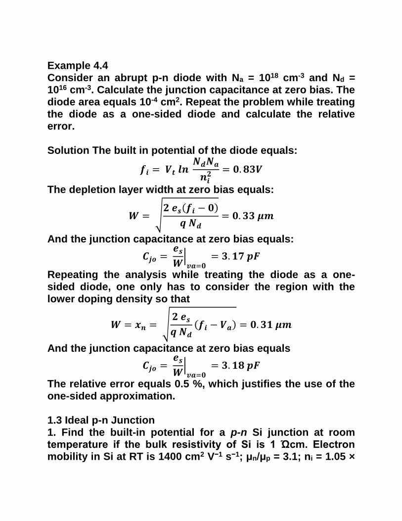
Example 4.4 Consider an abrupt p-n diode with Na = 1018 cm-3 and Nd = 1016 cm-3. Calculate the junction capacitance at zero bias. The diode area equals 10-4 cm2. Repeat the problem while treating the diode as a one-sided diode and calculate the relative error. Solution The built in potential of the diode equals:
𝒇𝒊 = 𝑽𝒕 𝒍𝒏 𝑵𝒅𝑵𝒂
𝒏𝒊𝟐 = 𝟎. 𝟖𝟑𝑽
The depletion layer width at zero bias equals:
𝑾 = √𝟐 𝒆𝒔(𝒇𝒊 − 𝟎)
𝒒 𝑵𝒅= 𝟎. 𝟑𝟑 𝝁𝒎
And the junction capacitance at zero bias equals:
𝑪𝒋𝒐 = 𝒆𝒔𝑾|𝒗𝒂=𝟎
= 𝟑. 𝟏𝟕 𝒑𝑭
Repeating the analysis while treating the diode as a one-sided diode, one only has to consider the region with the lower doping density so that
𝑾 = 𝒙𝒏 = √𝟐 𝒆𝒔𝒒 𝑵𝒅
(𝒇𝒊 − 𝑽𝒂) = 𝟎. 𝟑𝟏 𝝁𝒎
And the junction capacitance at zero bias equals
𝑪𝒋𝒐 = 𝒆𝒔𝑾|𝒗𝒂=𝟎
= 𝟑. 𝟏𝟖 𝒑𝑭
The relative error equals 0.5 %, which justifies the use of the one-sided approximation. 1.3 Ideal p-n Junction 1. Find the built-in potential for a p-n Si junction at room temperature if the bulk resistivity of Si is 1 Ώcm. Electron mobility in Si at RT is 1400 cm2 V−1 s−1; μn/μp = 3.1; ni = 1.05 ×

1010 cm−3. Solution: (3.1)
By definition, e𝝋𝒅 = Fn − Fp. Concentrations of the free carriers are given by
𝒏 = 𝑵𝒄 𝒆𝒙𝒑 (− 𝑬𝒈 − 𝑭𝒏
𝑲𝑻) , 𝑵𝒗 𝒆𝒙𝒑 (−
𝑬𝒈 − 𝑭𝒑
𝑲𝑻)
From here we get that
𝐞𝝋𝒅 = 𝑬𝒈 + 𝑲𝑻 𝒍𝒏 (𝒏
𝑵𝒄) + 𝑲𝑻 𝒍𝒏 (
𝒑
𝑵𝒗) = 𝑬𝒈 + 𝑲𝑻 𝒍𝒏 (
𝒏 𝒑
𝑵𝒄𝑵𝒗)
Since,
𝒏𝒊𝟐 = 𝑵𝒄 𝑵𝒗 𝒆𝒙𝒑 (−
𝑬𝒈
𝑲𝑻)
we obtain that
𝝋𝒅 = 𝑲𝑻
𝒆 𝒍𝒏 (
𝒏𝒑
𝒏𝒊𝟐)
From n = 1/e ρ μn and p = 1/e ρ μp, we finally get 𝝋𝒅 = 0.68 V. 6. At room temperature under the forward bias of 0.15 V the current through a p-n junction is 1.66 mA. What will be the current through the junction under reverse bias? Solution: (3.6) js = 1.66 mA exp(−eV/kT) = 4 μA. 7. For a p+-n Si junction the reverse current at room temperature is 0.9 nA/cm2. Calculate the minority-carrier lifetime if Nd = 1015 cm−3, ni = 1.05 × 1010 cm−3, and μp = 450 cm2 V−1 s−1. Solution: (3.7) For a p+-n junction

𝑱𝑺 = 𝒆 𝒑 𝑫𝒑
𝑳𝒑= 𝒆 𝒏𝒊
𝟐 𝑫𝒑
𝑵𝒅𝑳𝒑=𝒆 𝒏𝒊
𝟐
𝑵𝒅 (𝑫𝒑
𝝉𝒑)
𝟏𝟐⁄
Taking into account that μ = eD/kT, we finally get τp = 4.5 × 10⁻⁹ s. 1. Problem: A silicon p-n junction is formed between n-type Si doped with ND = 1017 cm-3and p-type Si doped with NA = 1016 cm-3. (a) Sketch the energy band diagram. Label all axes and all important energy levels. (b) Find nn0, np0, pp0, and pn0. Sketch the carrier concentration (of both electrons and holes) as a function of position. (c) Calculate the built-in potential Vbi in eV. Solution:
(a) The energy band diagram with labeled important energy levels and axes is
(b) Given n+= 1.5 x 1010 cm-3, in the quasi-neutral p-region,
Ppo = NA = 1016 cm−3
In the quasi-neutral n-region,
𝐧𝐧𝐨 = 𝐍𝐃 = 𝟏𝟎𝟏𝟕 𝐜𝐦−𝟑
In the depletion region,
𝐧𝐩𝐨 = 𝐧𝐢𝟐
𝐍𝐀 = 𝟐. 𝟐𝟓 𝐱𝟏𝟎𝟒 𝐜𝐦−𝟑
for p-side and
𝒑𝒏𝒐 = 𝒏𝒊𝟐
𝑵𝑫 = 𝟐. 𝟐𝟓 𝒙𝟏𝟎𝟑 𝒄𝒎−𝟑
for n-side.. The diagram for carrier concentration is:
ECp
Ei ECn
EF EVp Eg EVn
n(Xp) p(Xn) pn
Np 0 0

(b) The build-in potential is
𝐕𝐛𝐢 = 𝐊𝐓
𝐪𝐥𝐧𝐍𝐀𝐍𝐃
𝐧𝐢𝟐 =𝐊𝐓
𝐪𝐥𝐧𝐩𝐩
𝐩𝐧 = 𝟎. 𝟕𝟓𝟒 𝐞𝐕
Problem: 4 Consider a p+-n Si junction at T = 300 K with NA = 1018 cm-3 and ND = 1016 cm-3. The minority carrier hole diffusion constant is Dp = 12 cm2/s and the minority carrier hole lifetime is τp = 100 ns. The cross-sectional area of the junction is A = 10-4 cm2. Calculate the reverse saturation current Is = AJs. Calculate also the current at a forward bias Va = 0.5 V. Solution: Since NA >> ND, it is an asymmetric junction and the total current is dominated by the most heavily-doped side of the junction. the saturation current density is given by:
𝐉𝐬 = 𝐪 𝐃𝐩 𝐩𝐧𝐨
𝐋𝐩
Where,
𝐋𝐩 = (𝐃𝐩𝛕𝐩)𝟏𝟐⁄ = 𝟏. 𝟎𝟗𝟓 𝐱 𝟏𝟎−𝟑𝐜𝐦−𝟑 𝐚𝐧𝐝 𝐩𝐧𝐨 =
𝐧𝐢𝟐
𝐍𝐃= 𝟐. 𝟐𝟓 𝐱 𝟏𝟎−𝟑𝐜𝐦−𝟑
So, Js = 3:9492 x 10-11 A/cm2 Is = - A Js = - 3:9492 x 10-15 A
For a forward bias Va = 0.5 V, the current is:
𝐈 = 𝐈𝐬 (𝐞𝐪𝐕𝐨
𝐊𝐓⁄ − 𝟏 ) = 𝟖. 𝟗𝟑 𝛍𝐀
Problem (1) 1. n-Si with Nd = 7 × 1015 cm−3 additionally contains Nt = 1015 cm−3 generation- recombination centers located at the intrinsic Fermi level

with σn = σp = 10−15 cm2 and vt = 107 cm/s. Calculate generation rate, if 1. n and p are low as compared to the equilibrium value 2. only p is below the equilibrium value. For Si, ni = 1.05×1010 cm−3. Solution : By definition
𝑮𝒏 = − 𝑹𝒏 = 𝒏𝒊𝟐 − 𝒑 𝒏
𝝉𝒑(𝒏 + 𝒏𝒊) + 𝝉𝒏(𝒑 + 𝒑𝒊)
Where 𝝉𝒏−𝟏 = 𝝉𝒑
−𝟏 = 𝑵𝒕𝝈𝒏𝝂𝒕 = 𝟏𝟎𝟕𝒔−𝟏. In the first case n and p are less
than ni. Thus, np <𝒏𝒊𝟐 and hence
𝑮𝒏 = 𝒏𝒊𝟐
𝝉𝒏(𝒏𝒊 + 𝒑𝒊)=
𝒏𝒊𝟐 𝝉𝒏
= 𝟓. 𝟑 𝒙 𝟏𝟎𝟏𝟔𝒄𝒎−𝟑 /𝒔
In the second case n = Nd≫ni, whereas p <ni, hence
𝑮𝒏 = 𝒏𝒊𝟐
𝝉𝒏(𝒏 + 𝒏𝒊 + 𝒑𝒊)=
𝒏𝒊𝟐
𝝉𝒏 𝒏=
𝒏𝒊𝟐
𝝉𝒏𝑵𝒅= 𝟏. 𝟔 𝒙 𝟏𝟎𝟏𝟏𝒄𝒎−𝟑 /𝒔
Problem (2) Illumination of n-type Si (Nd = 1016 cm−3) generates 1021 cm−3/s electron-hole pairs. Si has Nt = 1015 cm−3 generation-recombination centers with σn = σp = 10−16 cm2. Calculate equilibrium concentration of electrons and holes if Et = Ei, where Ei is the Fermi level of intrinsic Si, and vt = 107 cm/s. Solution: In equilibrium, the generation G = 1021 cm−3/s and recombination R rates are equal
𝑮𝒏 = 𝑹 = 𝒏 𝒑 − 𝒏𝒊
𝟐
𝝉𝒑(𝒏 + 𝒏𝒊) + 𝝉𝒏(𝒑 + 𝒑𝒊)≈
𝒏 𝒑
𝝉𝒑 𝒏 + 𝝉𝒏 𝒑=
𝒏 𝒑
𝝉 (𝒏 + 𝒑)
Here we used 𝝉𝒏 = 𝝉𝒑 = 𝝉 = (Ntvtσn)−1 = 10−6 sec. In n-type Si under
illumination, n = Nd + ∆n, p ≈ ∆p = ∆n. Thus,
𝑮𝑻 = (𝑵𝒅 + ∆𝒏) ∆𝒏
𝑵𝒅 + 𝟐 ∆𝒏
Solving this equation with respect to ∆n we obtain p = ∆n = 1.1×1015 cm−3 and n = 1.1×1016 cm−3. SOLVED PROBLEMS
The reverse saturation current at 3ooK of a p-n Ge diode is 5 uA . Find

the voltage to be applied across the junction to obtain a forward current of 50 mA. Solution
𝑰 = 𝑰𝒔 [𝒆𝒙𝒑 (𝒆 𝑽
𝑲𝑻) − 𝟏]
So,
𝒆𝒙𝒑 (𝒆 𝑽
𝑲𝑻) =
𝑰
𝑰𝒔+ 𝟏 =
𝟓𝟎 𝒙 𝟏𝟎−𝟑
𝟓 𝒙 𝟏𝟎−𝟔+ 𝟏 = 𝟏𝟎𝟒
Or ,
𝑽 = 𝑲𝑻
𝒆 𝒍𝒏 𝟏𝟎𝟒 =
𝟏. 𝟑𝟖 𝒙 𝟏𝟎−𝟐𝟑 𝒙 𝟑𝟎𝟎
𝟏. 𝟔 𝒙 𝟏𝟎−𝟏𝟗 𝒙 𝟐. 𝟑𝟎𝟑 𝒙 𝟒 = 𝟎. 𝟐𝟑𝟖 𝑽𝒐𝒍𝒕
Problem (3) 3. A p+-n Si junction (ni = 1.05×1010 cm−3, ϵSi = 11.9) is formed in an n-type substrate with Nd = 1015 cm−3. If the junction contains 1015 cm−3 generation-recombination centers located at the intrinsic Fermi level with σn = σp = 10−15 cm2 (vt = 107 cm/s), calculate generation current density at a reverse bias of 10 V. Solution: Generation current in the space charge region w is given by
𝒋𝒈 = 𝒆 𝒏𝒊 𝝎
𝟐 𝝉
Here, 𝝉−1 = Ntσnvt = 107 s−1. The width w of the space charge region for a p+-n junction under reverse bias is
𝝎 = 𝝐 (𝝋𝒅 − 𝑽)
𝟐 𝝅 𝒆𝑵𝒅
𝟏𝟐⁄
≈ 𝝐 (𝑽)
𝟐 𝝅 𝒆 𝑵𝒅
𝟏𝟐⁄
= 𝟑. 𝟔 𝝁𝒎
Here we used relation |V|≫𝝋𝒅. From here we obtain that jg = 3 µA/cm2. Problem (4) For a p-n Si junction with the p-side doped to 1017 cm−3, the n-side doped to 1019 cm−3 (n+-p junction), and a reverse bias of −2 V, calculate the generation current density at room temperature,

assuming that the effective lifetime is 10−5 s.
Solution: Using the formulae of the previous problem and relation
𝝋𝒅 = 𝑲𝑻
𝒆 𝒍𝒏 (
𝑵𝟐
𝒏𝒊𝟐)
we get js = 1.6 nA/cm2.
Problem (5) For a p-n GaAs junction at room temperature find the donor/acceptor concentration at which de Broglie wavelength
(𝝀 = 𝟐 𝝅 𝒉
√𝟐 𝒎∗ 𝑬)
(𝑬 = 𝟑𝑲𝑻
𝟐) ,𝒎𝒆∗
𝒎𝒐= 𝟎. 𝟔𝟑 ,
𝒎𝒉∗
𝒎𝒐= 𝟎. 𝟓𝟑 𝒂𝒏𝒅 𝝐𝑮𝒂𝑨𝒔 = 𝟏𝟐. 𝟗 , 𝒏𝒊
𝑮𝒂𝑨𝒔
= 𝟐. 𝟏 𝒙 𝟏𝟎𝟔𝒄𝒎−𝟑 𝒂𝒏𝒅 𝑵𝑨 = 𝑵𝑫 Solution: From the parameters given, we find λn = 2.5×10⁻⁶ cm and λp = 8.5×10⁻⁷ cm. If Nd = Na = N the width of the space charge region is
𝝎 = 𝝐𝝋𝒅 𝝅 𝒆 𝑵
𝟏𝟐⁄
By definition, w = λ. Substituting
𝝋𝒅 = 𝑲𝑻
𝒆 𝒍𝒏 (
𝑵𝟐
𝒏𝒊𝟐)
into the expression above and after some simplifications, we get
𝑵 = 𝝐
𝝅 𝒆 𝝀𝟐𝟐 𝑲𝑻
𝒆 𝒍𝒏 (
𝑵
𝒏𝒊)
Solving the above equation numerically, we obtain N = 6.8 × 1018 cm−3 and 6.2×1019 cm−3 for electron and holes, respectively. Problem (6) When a silicon p+-n junction is reverse-biased to 30 V, the depletion-layer capacitance is 1.75 nF/cm2. If the maximum electric field at avalanche breakdown is 3×10⁵ V/cm, find the breakdown voltage. ϵSi = 11.9.
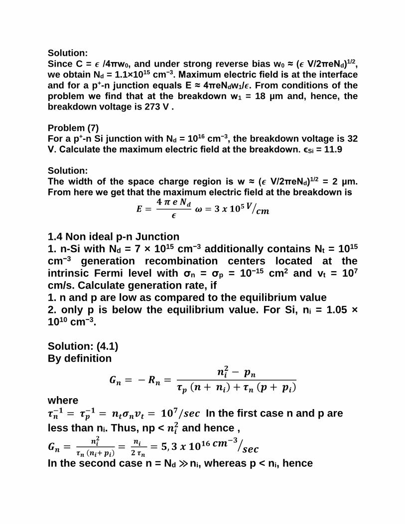
Solution: Since C = 𝝐 /4πw0, and under strong reverse bias w0 ≈ (𝝐 V/2πeNd)1/2, we obtain Nd = 1.1×1015 cm−3. Maximum electric field is at the interface and for a p+-n junction equals E ≈ 4πeNdw1/𝝐. From conditions of the problem we find that at the breakdown w1 = 18 µm and, hence, the breakdown voltage is 273 V . Problem (7) For a p+-n Si junction with Nd = 1016 cm−3, the breakdown voltage is 32 V. Calculate the maximum electric field at the breakdown. ϵSi = 11.9 Solution: The width of the space charge region is w ≈ (𝝐 V/2πeNd)1/2 = 2 µm. From here we get that the maximum electric field at the breakdown is
𝑬 = 𝟒 𝝅 𝒆 𝑵𝒅
𝝐 𝝎 = 𝟑 𝒙 𝟏𝟎𝟓 𝑽 𝒄𝒎⁄
1.4 Non ideal p-n Junction 1. n-Si with Nd = 7 × 1015 cm−3 additionally contains Nt = 1015 cm−3 generation recombination centers located at the intrinsic Fermi level with σn = σp = 10−15 cm2 and vt = 107 cm/s. Calculate generation rate, if 1. n and p are low as compared to the equilibrium value 2. only p is below the equilibrium value. For Si, ni = 1.05 × 1010 cm−3. Solution: (4.1) By definition
𝑮𝒏 = − 𝑹𝒏 = 𝒏𝒊𝟐 − 𝒑𝒏
𝝉𝒑 (𝒏 + 𝒏𝒊) + 𝝉𝒏 (𝒑 + 𝒑𝒊)
where
𝝉𝒏−𝟏 = 𝝉𝒑
−𝟏 = 𝒏𝒕𝝈𝒏𝒗𝒕 = 𝟏𝟎𝟕/𝒔𝒆𝒄 In the first case n and p are
less than ni. Thus, np < 𝒏𝒊𝟐 and hence ,
𝑮𝒏 = 𝒏𝒊𝟐
𝝉𝒏 (𝒏𝒊+ 𝒑𝒊)=
𝒏𝒊𝟐 𝝉𝒏
= 𝟓, 𝟑 𝒙 𝟏𝟎𝟏𝟔 𝒄𝒎−𝟑
𝒔𝒆𝒄⁄
In the second case n = Nd ≫ ni, whereas p < ni, hence

𝑮𝒏 = 𝒏𝒊𝟐
𝝉𝒏 (𝒏 + 𝒏𝒊 + 𝒑𝒕)=
𝒏𝒊𝟐
𝒏 𝝉𝒏 =
𝒏𝒊𝟐
𝝉𝒏𝑵𝒅 = 𝟏, 𝟔 𝒙 𝟏𝟎𝟏𝟏 𝒄𝒎
−𝟑
𝒔𝒆𝒄⁄
2. Illumination of n-type Si (Nd = 1016 cm−3) generates 1021 cm−3/s electron-hole pairs. Si has Nt = 1015 cm−3 generation-recombination centers with σn = σp = 10−16 cm2. Calculate equilibrium concentration of electrons and holes if Et = Ei, where Ei is the Fermi level of intrinsic Si, and vt = 107 cm/s. Solution: (4.2) In equilibrium, the generation G = 1021 cm−3/s and recombination R rates are equal,
𝑮 = 𝑹 = 𝒏 𝒑 − 𝒏𝒊
𝟐
𝝉𝒑 (𝒏 + 𝒏𝒊) + 𝝉𝒏 (𝒑 + 𝒏𝒊) ≈
𝒏 𝒑
𝝉𝒑𝒏 + 𝝉𝒏𝒑
= (𝒏 𝒑)/𝝉( 𝒏 + 𝒑) Here we used 𝝉𝒏 = 𝝉𝒑 = 𝝉 = (Nt vt σn)−1 = 10−6 sec.
In n-type Si under illumination, n = Nd + Δn , p ≈ Δp = Δn. Thus,
𝑮𝑻 = (𝑵𝒅 + ∆ 𝒏)∆𝒏
𝑵𝒅 + 𝟐 ∆ 𝒏
Solving this equation with respect to Δn we obtain p = Δn = 1.1×1015 cm−3 and n = 1.1 × 1016 cm−3. 3. A p+-n Si junction (ni = 1.05×1010 cm−3, ε = 11.9) is formed in an n-type substrate with Nd = 1015 cm−3. If the junction contains 1015 cm−3 generation-recombination centers located at the intrinsic Fermi level with σn = σp = 10−15 cm2 (vt = 107 cm/s), calculate generation current density at a reverse bias of 10 V. Solution: (4.3) Generation current in the space charge region w is given by
𝒋𝒈 = 𝒆 𝒏𝒊 𝒘
𝟐 𝝉

Here, τ−1 = Nt σn vt = 107 s−1. The width w of the space charge region for a p+-n junction under reverse bias is
𝒘 = (𝝐 (𝝋𝒅 − 𝑽)
𝟐 𝝅 𝑵𝒅)
𝟏𝟐⁄
≈ (𝝐 |𝐕 |
𝟐 𝝅 𝒆 𝑵𝒅)
𝟏𝟐⁄
= 𝟑. 𝟔 𝝁𝒎
Here we used relation |V | ≫ 𝝋𝒅. From here we obtain that jg = 3 μA/cm2. 4. For a p-n Si junction with the p-side doped to 1017 cm−3, the n-side doped to 1019 cm−3 (n+-p junction), and a reverse bias of −2 V, calculate the generation current density at room temperature, assuming that the effective lifetime is 10−5 s. Solution: (4.4) Using the formulae of the previous problem and relation
𝝋𝒅 = 𝑲𝑻
𝒆 𝒍𝒏 (
𝒏 𝒑
𝒏𝒊𝟐 )
we get js = 1.6 nA/cm2. 5. For a p-n GaAs junction at room temperature find the donor/acceptor concentration at which de Broglie wavelength (λ = 2πh /√2m* E) of electrons/holes is equal to the width of the space charge region. Assume <Ei > 3 kT/2, m*
e/m0 = 0.063, m*h/m0 = 0.53, and εGaAs = 12.9, nGaAs
i = 2.1 × 106 cm−3, and Na = Nd.
Part (14) Solved PROBLEMS The transition capacitance , The diffusion capacitance Example 4.5 a. Calculate the diffusion capacitance of the diode described

in Example 4.4 at zero bias. Use µn = 1000 cm2/V-s, µp = 300 cm2/V-s, wp' = 1 µm and wn' = 1 mm. The minority carrier lifetime equals 0.1 ms. b. For the same diode, find the voltage for which the junction capacitance equals the diffusion capacitance. Solution a. The diffusion capacitance at zero volts’ equals
𝑪𝒅,𝟎 = 𝑰𝒔,𝒑𝝉𝒑
𝑽𝒕+ 𝑰𝒔,𝒏𝝉𝒏𝑽𝒕
= 𝟏. 𝟕𝟑 𝒙 𝟏𝟎−𝟏𝟗𝑭
Using
𝑰𝒔,𝒑 = 𝒒 𝑨𝒑𝒏𝒐𝑫𝒑
𝑳𝒑
And ,
𝑰𝒔𝒏 = 𝒒 𝑨𝒏𝒑𝒐𝑫𝒏
𝑾𝒑
Where the "short" diode expression was used for the capacitance associated with the excess charge due to electrons in the p-type region. The "long" diode expression was used for the capacitance associated with the excess charge due to holes in the n-type region. The diffusion constants and diffusion lengths equal Dn = µn x Vt = 25.8 cm2/s Dp = µp x Vt = 7.75 cm2/s
𝑳𝒑 = √𝑫𝒑𝝉𝒑
And the electron transit time in the p-type region equals
𝝉𝒓,𝒏 = 𝒘𝒑𝟐
𝟐 𝑫𝒏= 𝟏𝟗𝟑 𝒑𝒔
b. The voltage at which the junction capacitance equals the diffusion capacitance is obtained by solving

𝑪𝒋𝒐
√𝟏 − 𝑽𝒂
𝒇𝒊
= 𝑪𝒅,𝟎𝒆𝑽𝒎
𝑽𝒕⁄
yielding Va = 0.442 V 2. For the p-n Si junction from the previous problem calculate the width of the space charge region for the applied voltages V = −10, 0, and +0.3 V. εSi = 11.9 Solution: (3.2) Taking into account that at room temperature all donors and acceptors are ionized, i.e. n = Nd and p = Na, from the values found in the previous problem and
𝝎 = (𝝐(𝝋𝒅 − 𝑽)
𝟐 𝝅 𝒆 𝑵𝒅+ 𝑵𝒂𝑵𝒅𝑵𝒂
)
𝟏𝟐⁄
we get ω(−10V) = 2 μm , ω(0V) = 0.5 μm , and ω(+0.3V) = 0.4 μm. 3. For the parameters given in the previous problem find the maximum electric field within the space charge region. Compare these values with the electric field within a shallow donor: E ≈ e/εSia2
B, where aB is the Bohr radius of a shallow donor, aB =εSih2
/m* e e2 and me /mo = 0.33. Solution: (3.3)
𝑬 = 𝟐 (𝟐 𝝅 𝒆 (𝝋𝒅 − 𝑽)
𝝐 𝑵𝒅 𝑵𝒂𝑵𝒅 +𝑵𝒂
)
𝟏𝟐⁄
we obtain that E(−10V) = 105 V/cm, E(0V) = 2.6×10⁴ V/cm, and E(+0.3V) = 2 × 10⁴ V/cm. The electric field within a shallow donor is, in turn, E ≈ 3.4 × 10⁵ V/cm, that is, comparable to that of the p-n junction.

4. Calculate the capacity of the p-n junction from the problem 2 if the area of the junction is 0.1 cm2. Solution: (3.4)
𝐂 = 𝛜 𝐒
𝟒 𝛑 𝛚 .
we get C(−10V) = 0.5 nF, C(0V) = 2 nF, and C(+0.3V) = 2.6 nF. 5. n-Si of a p-n Si junction has a resistivity of 1 Ώcm. What should be the resistivity? of p-Si so that 99 % of the total width of the space charge region would be located in n-Si (p+-n junction)? For the parameters needed see problem 1. Solution: (3.5) From the conditions of the problem ωa = 0.01ω and ωd = 0.99ω. Since ωa/ωd = Nd/Na , we get that Na = 99 Nd. Because Nd = 1/eρμn = 4.5 × 1015 cm−3, we get Na = 4.4 × 1017 cm−3.
Solution: (4.5) From the parameters given, we find λn = 2.5 × 10⁻⁶ cm and λp = 8.5 × 10⁻⁷ cm. If Nd = Na = N the width of the space charge region is
𝒘 = (𝝐 𝝋𝒅
𝝅 𝒆 𝑵)
𝟏𝟐⁄
By definition, w = λ. Substituting
𝝋𝒅 = 𝑲𝑻
𝒆 𝒍𝒏 (
𝑵𝟐
𝒏𝒊𝟐)
into the expression above and after some simplifications, we get
𝑵 = 𝝐
𝝅 𝒆𝝀𝟐 𝟐 𝑲𝑻
𝒆𝒍𝒏 (
𝑵
𝒏𝒊)
Solving the above equation numerically, we obtain N = 6.8 ×

1018 cm−3 and 6.2 × 1019 cm−3 for electron and holes, respectively. 6. When a silicon p+-n junction is reverse-biased to 30 V, the depletion-layer capacitance is 1.75 nF/cm2. If the maximum electric field at avalanche breakdown is 3 × 10⁵ V/cm, find the breakdown voltage. εSi = 11.9. Solution: (4.6) Since C = ϵ / 4 π w0, and under strong reverse bias w0 ≈ (ϵ V / 2 π e Nd)1/2, we obtain Nd = 1.1 × 1015 cm−3. Maximum electric field is at the interface and for a p+-n junction equals E ≈ 4 π e Nd w1 / ϵ. From conditions of the problem we find that at the breakdown w1 = 18 μm and, hence, the breakdown voltage is 273 V . 7. For a p+-n Si junction with Nd = 1016 cm−3, the breakdown voltage is 32 V. Calculate the maximum electric field at the breakdown. εSi = 11.9. Solution: (4.7) The width of the space charge region is w ≈ (ϵV / 2πeNd)1/2= 2 μm. From here we get that the maximum electric field at the breakdown is
𝑬 = 𝟒𝛑𝐞𝐍𝐝
𝛜 𝒘 ≈ 𝟑 𝐱 𝟏𝟎𝟓 𝑽 𝒄𝒎⁄
Problem:2 A Si p-n junction has dopant concentrations ND = 2 x 1015 cm-3 and NA
= 2 x 1016 cm-3. Calculate the built-in potential Vbi in eV and the total width of the depletion region W = xn0 + xp0 at zero bias (that is, Va = 0) and under a reverse bias Va = - 8V.
Solution: (a) Given ni = 1:5 x 1010 cm-3, the build-in potential is:

𝑽𝒃𝒊 = 𝑲𝑻
𝒒𝐥𝐧𝑵𝑨𝑵𝑫
𝒏𝒊𝟐 =𝑲𝑻
𝒒𝐥𝐧𝒑𝒑
𝒑𝒏 = 𝟎. 𝟔𝟕𝟏 𝒆𝑽
(b) The depletion width with a bias Va is give by:
𝑾 = √𝟐 𝝐𝒐 (𝑽𝒃𝒊 − 𝑽𝒂)
𝒒 (𝟏
𝑵𝑨+
𝟏
𝑵𝑫)
For Va = 0V , we have W = 0:691µm and for Va = - 8V , we have W = 2:475 µm. Problem: 3 A Si p-n junction is reverse-biased with Va = -10V . Determine the percent change in junction (depletion) capacitance and built-in potential if the doping in the p region is increased by a factor of 2. Solution: Let us assume the NA and ND values are ND = 2 x 1015 cm-3 and NA = 2 x 1016 cm-3 , then the build-in potential is calculated by the equation, we have:
𝑽𝒃𝒊 = 𝑲𝑻
𝒒𝐥𝐧𝑵𝑨𝑵𝑫
𝒏𝒊𝟐 =𝑲𝑻
𝒒𝐥𝐧𝒑𝒑
𝒑𝒏 = 𝟎. 𝟔𝟕𝟏 𝒆𝑽
and
𝑽𝒃𝒊 = 𝑲𝑻
𝒒𝐥𝐧(
𝟐 𝑵𝑨𝑵𝑫
𝒏𝒊𝟐 ) = 𝟎: 𝟔𝟖𝟖𝟖 𝒆𝑽
Therefore, Vbi is increased by 2:67%. The depletion capacitance can be calculated by
𝑪𝒋 = 𝝐 𝑨
𝑾
Where A is the cross-sectional area of the junction and W is the depletion width calculated by:
𝑾 = √𝟐 𝝐𝒐 (𝑽𝒃𝒊− 𝑽𝒂)
𝒒 (
𝟏
𝑵𝑨+
𝟏
𝑵𝑫) = 2:7549 µm
𝑾 = √𝟐 𝝐𝒐 (𝑽𝒃𝒊− 𝑽𝒂)
𝒒 (
𝟏
𝟐 𝑵𝑨+
𝟏
𝑵𝑫) = 2:6938 µm
Therefore, the percent change in junction depletion capacitance is given by:
𝑪𝒋, − 𝑪𝒋
𝑪𝒋= 𝒘 − 𝒘.
𝒘.= 𝟐. 𝟐𝟕 %

Switching time
Example 1.8 Determine the current ID and the diode voltage VD for the circuit shown with VDD=5V and R=1 K . Assume that the diode has a current of 1 mA at a voltage of 0.7V and that its voltage drop changes by 0.1V for every decade change in current. To begin the iteration, we assume that VD = 0.7 V and use the next equation to determine the current. ID R + VDD vd - Assuming that VDD is greater than 0.5 V or so, the diode current will be much greater than Is, and we can represent the diode i-v characteristic by the exponential relationship, resulting in
𝑰𝑫 = 𝑰𝒔 𝒆𝑽𝑫
𝜼 𝑽𝑻⁄
The other equation that governs circuit operation is obtained by writing a Kirchhoff loop equation, resulting in
𝑰𝑫 𝑽𝑫𝑫 − 𝒗𝑫
𝑹
Assuming that the diode parameters Is and n are known , the two equations above has two unknown quantities ID and VD. Two alternative ways for obtaining the solution are graphical analysis and iterative analysis.
Graphical Analysis Using the Exponential Model
i VDD/R Load line Diode characteristics Q ID operating point Slope = 1/R

Graphical analysis is performed by plotting the relationships of the used equations above on the i-v plane. The solution can then be obtained as the coordinates of the point of intersection of the two graphs. A sketch of the graphical construction is shown. The curve represents the exponential diode equation, and the straight line is known as the l o a d line. The load line intersects the diode curve at point Q, which represents the operating point of the circuit. Its coordinates give the values of ID and VD. Example 1.8 Determine the current ID and the diode voltage VD for the circuit shown ID R + VDD vd - With VDD=5V and R = 1 K . Assume that the diode has a current of 1 mA at a voltage of 0.7V and that its voltage drop changes by 0.1V for every decade change in current. To begin the iteration, we assume that VD = 0.7 V and determine the current
𝑰𝑫 𝑽𝑫𝑫 − 𝒗𝑫
𝑹= 𝟓 − 𝟎. 𝟕
𝟏= 𝟒. 𝟑 𝒎𝑨
We then use the diode equation to obtain a better estimate for VD. This can be done by employing Eq. as
𝑽𝟐 − 𝑽𝟏 = 𝟐𝟑 𝜼 𝑽𝑻 𝒍𝒐𝒈 𝒊𝟏𝒊𝟐⁄

𝟐𝟑 𝜼 𝑽𝑻 = 𝟎. 𝟏 𝑽 , 𝒕𝒉𝒖𝒔 𝑽𝟐 = 𝑽𝟏 + 𝟎. 𝟏 𝒍𝒐𝒈𝒊𝟏𝒊𝟐⁄
Substituting V1 = 0.7 V, I1 = 1 mA, and I2 = 4.3 mA results in V2 = 0.763 V. Thus the results of the first iteration are ID = 4.3 mA and VD = 0.763 V. The second iteration proceeds in a similar manner:
𝑰𝑫 𝑽𝑫𝑫 − 𝒗𝑫
𝑹= 𝟓 − 𝟎. 𝟕𝟔𝟑
𝟏= 𝟒. 𝟐𝟑𝟕 𝒎𝑨
𝑽𝟐 = 𝟎. 𝟕𝟔𝟑 + 𝟎. 𝟏 𝒍𝒐𝒈 𝟒. 𝟐𝟑𝟕
𝟒. 𝟑= 𝟎. 𝟕𝟔𝟐 𝑽
Thus the second iteration yields ID = 4.237 mA and VD = 0.762 V. Since these values are not much different from the values obtained after the first iteration, no further iterations are necessary, and the solution is ID = 4.237 mA and VD = 0.762 V. Example 11 The dc power supply circuit of figure shown is to be designed for the following specifications: dc output voltage = +15 V, dc load current = 100 mA, and percent ripple = 5%. The rectifier diode can be modeled with the parameters VD0 = 0.7 V and RD = 0. Calculate the required transformer secondary ac rms voltage and the value of the filter capacitor. Assume a frequency f = 60 Hz.
Solution. The peak secondary transformer voltage is given by V1 = 15+0.7 = 15.7 V. The ac rms voltage is 15.7/ √ 2 = 11.1 V rms. The effective value of the load resistor is RL = 15 / 0.1 = 150 Ω. The value of C can be
calculated form equation 𝑷𝒆𝒓𝒄𝒆𝒏𝒕 𝑹𝒊𝒑𝒑𝒍𝒆 ≤ [𝟏 − 𝒆𝒙𝒑 (− 𝑻
𝑹𝑳 𝑪)] 𝒙 𝟏𝟎𝟎 %
Where equality used. We obtain
iL (t) + + To AC vS (t) Power C RL vL(t) Line - -

𝑪 = 𝑻
𝑹𝑳
− 𝟏
𝒍𝒏 (𝟏 − % 𝒓𝒊𝒑𝒑𝒍𝒆
𝟏𝟎𝟎)= 𝟏𝟓𝟎⁄
𝟏𝟓𝟎
−𝟏
𝒍𝒏 (𝟏 − 𝟓 𝟏𝟎𝟎⁄ )= 𝟐𝟏𝟕𝟎 𝝁𝑭
If follows from the inequality equation 𝑷𝒆𝒓𝒄𝒆𝒏𝒕 𝑹𝒊𝒑𝒑𝒍𝒆 ≤ [𝟏 −
𝒆𝒙𝒑 (− 𝑻
𝑹𝑳 𝑪)] 𝒙 𝟏𝟎𝟎 % that this value for C gives a percent ripple that is
less than 5%.
Part (15) Solved PROBLEMS photoelectric effect Problem (1) (a) An electron beam strikes a crystal of cadmium sulfide (CdS). Electrons scattered by the crystal move at a velocity of 4.4 x 10⁵ m/s. Calculate the energy of the incident beam. Express your result in eV. CdS is a semiconductor with a band gap, Eg, of 2.45 eV. (b) Cadmium telluride (CdTe) is also a semiconductor. Do you expect the band gap of this material to be greater or less than the band gap of CdS? Explain. Solution (a)

𝑬𝒊𝒏𝒄𝒊𝒅𝒆𝒏𝒕 𝒆− = 𝑬𝒆𝒎𝒊𝒕𝒕𝒆𝒅 𝒗 + 𝑬𝒔𝒄𝒂𝒕𝒕𝒆𝒓𝒆𝒅 𝒆− = 𝑬𝒈 + 𝒎 𝒗𝟐
𝟐
𝑬𝒊𝒏𝒄𝒊𝒅𝒆𝒏𝒕 𝒆− = 𝟐. 𝟒𝟓 𝒆𝑽 +𝟏
𝟐 𝒙 𝟗. 𝟏𝟏 𝒙 𝟏𝟎−𝟑𝟏 𝒌𝒈 𝒙 (𝟒. 𝟒 𝒙 𝟏𝟎𝟓
𝒎
𝒔)𝟐
𝟏. 𝟔 𝒙 𝟏𝟎−𝟏𝟗𝒆𝑽
𝑱
= 𝟐. 𝟒𝟓 𝒆𝑽 + 𝟎. 𝟓𝟓 𝒆𝑽 = 𝟑 𝒆𝑽 (b) Eg(CdTe) <Eg(CdS) The Cd–S bond is stronger than Cd–Te bond because although both S and Te are group 16, Te is much larger than S. Problem #8 The energy gap (Eg) of ZnSe is 2.3 eV. (a) Is this material transparent to visible radiation? Substantiate your answer. (b) How could you increase the electrical conductivity of this material? Give the reasons for the effectiveness of your suggested approach. Solution
Escattered e-
Eincident e- scattered
Eg
Eemitted photons
e-
incident CdS crystal

(a) The optical properties of ZnSe can be explained when comparing the energy band of the visible spectrum with the energy band diagram of ZnSe. Absorption takes place via photo excitation for all radiation with E ≥ 2.3 eV. From the energy distribution of the visible spectrum we recognize that the blue– green portion has photon energies in excess of the band gap (Eg = 2.3eV) and thus will be absorbed. The yellow–red potion, on the other hand, has photon energies less than the band gap – it will be transmitted. ZnSe, therefore, is expected to exhibit a yellowish–red color. (b) In principle there are two ways to increase the electrical conductivity of ZnSe: a. A temperature rise. Any rise in temperature will increase the number of “thermally activated” charge carriers in the conduction band (electrons) and in the valence band (holes) and, thus, the electronic conductivity. Aside: The electrical conductivity of solids, demonstrated by the flow of electronic charge carriers under an applied electric field (E), can be
ʎ (Ao) CB 4000 5397 7000 E(hv) Eg= 2.3 eV E 3.1 2.3 2.26 1.77 E (eV) Absorb Blue green yellow red Absorbed 1 transmitted 0 5397 ʎ (Ao) wave length

formulated through Ohm’s law, J = σE, which states that the current density (J = number of charges transported through a unit area in a unit time) is proportional (σ = conductivity) to the applied electric field. Accordingly:
𝑱 = 𝑵 𝒆 𝒗𝒅 where N = number of charge carriers/unit volume, e = electronic charge and vd = average drift velocity of charge carriers in an applied electric field. We thus obtain:
𝝈 =𝑵 𝒆 𝒗𝒅𝑬
and if we define d(v /E) = μ, the charge carrier mobility, we have: σ = N e μ
In intrinsic semiconductors we have both electrons and holes contributing to conduction: e e n h e h σ = Ne e μe + Nneμh = Ne(μe + μh ) since Ne = Nh. Taking the number of thermally generated charge carriers, given by the relationship
𝑵 = 𝑨𝑻𝟑𝟐 ⁄ 𝒆
−𝑬𝒈𝟐 𝑲𝑻⁄
we obtain the temperature dependence of the conductivity as:
𝝈 = 𝑨𝑻𝟑𝟐 ⁄ 𝒆
−𝑬𝒈𝟐 𝑲𝑻⁄ 𝒙 𝐞 (𝝁𝒆 + 𝝁𝒉 )
To assess the temperature dependence of electrical conductivity we must take into consideration that, because of increased vibration of the atoms about their lattice positions, the charge carrier mobility will decrease (increased scattering of charge carriers) with increasing temperature. This effect explains why the electronic conductivity in metals, where N is constant, will decrease with increasing temperature. In semiconductors, where N increases with temperature, the accompanying mobility effect is not apparent at low temperatures (conductivity increases), but becomes pronounced at high temperatures (conductivity decreases). b. Introduction of shallow impurity (or defect) states close to the conduction or valence band. This is accomplished by the incorporation of appropriate dopant elements into the crystal matrix. If these impurities are shallow (~0.01 eV from the conduction or valence band), they will be totally ionized at room temperature and each will contribute an electron (donor dopant: K, Na) or holes

(acceptor dopant: G, Br), thus increasing the electrical conductivity without the necessity of a temperature rise. (Be aware that certain defects in the crystal lattice may also increase the electronic conductivity.) 9. Electron mobility in Si is 1400 cm2 V−1s−1. Calculate the mean free time in scattering (Relaxations time) of electrons. Effective mass is m∗
e/m0 = 0.33. Solution: From µ = eτ/m∗ we get that τ = 2.6×10⁻¹³ s.
Example 1.1 A metal has a work function of 4.3 V. What is the minimum photon energy in Joule to emit an electron from this metal through the photo-electric effect? What are the photon frequency in Terahertz and the photon wavelength in micrometer? What is the corresponding photon momentum? What is the velocity of a free electron with the same momentum? Solution The minimum photon energy, Eph, equals the work function, ΦM, in units of electron volt or 4.3 eV. This also equals:
𝑬𝒑𝒉 = 𝒒 𝝓𝒎 = 𝟏. 𝟔 𝒙 𝟏𝟎−𝟏𝟗 𝒙 𝟒. 𝟑 = 𝟔. 𝟖𝟗 𝒙 𝟏𝟎−𝟏𝟗
The corresponding photon frequency is:
𝒇𝒑𝒉 = 𝟔. 𝟖𝟗 𝒙 𝟏𝟎−𝟏𝟗
𝟔. 𝟔𝟐𝟔 𝒙 𝟏𝟎−𝟑𝟒= 𝟏𝟎𝟒𝟎 𝑻𝑯𝒛
The corresponding wavelength equals:
𝝀 =𝒉 𝒄
𝑬𝒑𝒉= 𝟔. 𝟔𝟐𝟔 𝒙 𝟏𝟎−𝟑𝟒 𝒙 𝟑 𝒙 𝟏𝟎𝟖
𝟔. 𝟖𝟗 𝒙 𝟏𝟎−𝟏𝟗=
𝟏. 𝟐𝟒 𝝁
𝑬𝒑𝒉 (𝒆𝑽)= 𝟎. 𝟐𝟖𝟖 𝝁𝒎
The photon momentum, p, is:
𝒑 =𝒉
𝝀= 𝟔. 𝟔𝟐𝟔 𝒙 𝟏𝟎−𝟑𝟒
𝟎. 𝟐𝟖𝟖 𝒙 𝟏𝟎−𝟔= 𝟐. 𝟐𝟗𝟕 𝒙 𝟏𝟎−𝟐𝟕 𝒌𝒈 𝒎/𝒔

And the velocity, v, of a free electron with the same momentum equals:
𝝂 = 𝒑
𝒎𝒐= 𝟐. 𝟐𝟗𝟕 𝒙 𝟏𝟎−𝟐𝟕
𝟗. 𝟏𝟏 𝒙 𝟏𝟎−𝟑𝟏= 𝟐𝟓𝟐𝟐 𝒎/𝒔
Where mo is the free electron mass
𝑬𝒑𝒉 = 𝒒 𝝓𝒎 = 𝟏. 𝟔 𝒙 𝟏𝟎−𝟏𝟗 𝒙 𝟒. 𝟑 = 𝟔. 𝟖𝟗 𝒙 𝟏𝟎−𝟏𝟗
Example 1.2 (the blackbody radiation) The spectral density of the sun peaks at a wavelength of 900 nm. If the sun behaves as a black body, what is the temperature of the sun? Solution: A wavelength of 900 nm corresponds to a photon energy of:
𝑬𝒑𝒉 =𝒉 𝒄
𝝀=𝟔. 𝟔𝟐𝟔 𝒙 𝟏𝟎−𝟑𝟒 𝒙 𝟑 𝒙 𝟏𝟎𝟖
𝟗𝟎𝟎 𝒙 𝟏𝟎−𝟗= 𝟐. 𝟐𝟏 𝒙 𝟏𝟎−𝟏𝟗𝑱𝒐𝒖𝒍𝒆
Since the peak of the spectral density occurs at 2.82 kT, the corresponding temperature equals:
𝑻 = 𝑬𝒑𝒉
𝟐. 𝟖𝟐 𝒌=
𝟐. 𝟐𝟏 𝒙 𝟏𝟎−𝟏𝟗
𝟐. 𝟖𝟐 𝒙 𝟏. 𝟑𝟖 𝒙𝟏𝟎−𝟐𝟑= 𝟓𝟔𝟕𝟐 𝑲𝒆𝒍𝒗𝒊𝒏
Example 1.3 An electron is confined to a 1 micron thin layer of silicon. Assuming that the semiconductor can be adequately described by a one-dimensional quantum well with infinite walls, calculate the lowest possible energy within the material in units of electron volt. If the energy is interpreted as the kinetic energy of the electron, what is the corresponding electron velocity? (The effective mass of electrons in silicon is 0.26 m0, where m0 = 9.11 x 10⁻³¹ kg is the free electron rest mass).

Solution: The lowest energy in the quantum equals:
𝑬𝟏 = 𝒉𝟐
𝟐 𝒎∗(𝟏
𝟐 𝑳𝒑)
𝟐
= (𝟔. 𝟔𝟐𝟔 𝒙 𝟏𝟎−𝟑𝟒)𝟐
𝟐 𝒙 𝟎. 𝟐𝟔 𝒙 𝟗. 𝟏𝟏 𝒙 𝟏𝟎−𝟑𝟏(
𝟏
𝟐 𝒙 𝟏𝟎−𝟔)𝟐
= 𝟐. 𝟑𝟐𝒙 𝟏𝟎−𝟐𝟓𝒋𝒐𝒖𝒍𝒆 = 𝟏. 𝟒𝟓 𝒎𝒆𝑽 Then velocity of an electron with this energy equal:
𝝂 = √𝟐𝑬𝟏𝒎∗
= √𝟐 𝒙 𝟐. 𝟑𝟐 𝒙 𝟏𝟎−𝟐𝟓
𝟎. 𝟐𝟔 𝒙 𝟗. 𝟏𝟏 𝒙 𝟏𝟎−𝟑𝟏= 𝟏. 𝟑𝟗𝟗 𝒌𝒎/𝒔
Example 1.4 Consider an infinitely long cylinder with charge density r, dielectric constant ε0 and radius r0. What is the electric field in and around the cylinder? Solution: Because of the cylinder symmetry one expects the electric field to be only dependent on the radius, r. Applying Gauss's law one finds:
= 𝜺 𝟐 𝝅 𝒓 𝑳 = 𝑸
𝜺𝟎= 𝝆 𝝅 𝒓𝟐 𝑳
𝜺𝒐
And
= 𝜺 𝟐 𝝅 𝒓 𝑳 = 𝑸
𝜺𝟎= 𝝆 𝝅 𝒓𝒐
𝟐 𝑳
𝜺𝒐
Where a cylinder with length L was chosen to define the surface A and edges effects were ignored. the electric field then equal:
𝜺(𝒓) = 𝝆 𝒓
𝟐 𝜺𝒐
The electric field increases with the cylinder with increasing radius. The electric field decreases outside with the cylinder with increasing radius.

Problem 1.1 Calculate the wavelength of a photon with a photon energy of 2 eV. Also, calculate the wavelength of an electron with a kinetic energy of 2 eV. Solution The wavelength of a 2 eV photon equals:
𝐝𝐞𝐁𝐫𝐨𝐠𝐥𝐢𝐞𝒍𝒘 =𝒉 𝑪
𝑬𝒑𝒉= 𝟔. 𝟔𝟐𝟔 𝒙 𝟏𝒐−𝟑𝟒 𝑱 𝒙 𝟑 𝒙 𝟏𝟎𝟖 𝒎/𝒔𝒆𝒄
𝟏. 𝟔𝟎𝟐 𝒙 𝟏𝟎−𝟏𝟗 𝒄 𝟐 𝒆𝑽⁄
= 𝟎. 𝟔𝟐 𝝁𝒎 where the photon energy (2 eV) was first converted to Joules by multiplying with the electronic charge. The wavelength of an electron with a kinetic energy of 2 eV is obtained by calculating the deBroglie wavelength:
𝐝𝐞𝐁𝐫𝐨𝐠𝐥𝐢𝐞𝒍𝒘 =𝒉
𝒑=
𝟔. 𝟔𝟐𝟔 𝒙 𝟏𝒐−𝟑𝟒 𝑱
𝟕. 𝟔𝟐 𝒙 𝟏𝟎−𝟐𝟓𝒌𝒈 𝒎
𝒔⁄= 𝟎. 𝟖𝟕𝒏𝒎
Where the momentum of the particle was calculated from the kinetic energy:
𝒑 = √𝟐 𝒎 𝑬 = √𝟐 𝒙 𝟗. 𝟏𝟏 𝒙 𝟏𝒐−𝟑𝟏 𝒌𝒈 𝒙 𝟏. 𝟔 𝒙 𝟏𝟎−𝟏𝟗 𝒄 𝒙 𝟐 𝒆𝑽= 𝟕. 𝟔𝟒 𝒙 𝟏𝟎−𝟐𝟓 𝒌𝒈 𝒎/𝒔
Problem 1.2 Consider a beam of light with a power of 1 Watt and a wavelength of 800 nm. Calculate a) the photon energy of the photons in the beam, b) the frequency of the light wave and c) the number of photons provided by the beam in one second. Solution The photon energy is calculated from the wavelength as:
𝑬𝒑𝒉 = 𝒉 𝑪
𝐝𝐞𝐁𝐫𝐨𝐠𝐥𝐢𝐞𝒍𝒘= 𝟔. 𝟔𝟐𝟔 𝒙 𝟏𝒐−𝟑𝟒 𝑱𝒔 𝒙 𝟑 𝒙 𝟏𝟎𝟖 𝒎/𝒔
𝟖𝟎𝟎 𝒙 𝟏𝟎−𝟗 𝒎= 𝟐. 𝟒𝟖 𝒙 𝟏𝟎−𝟏𝟗𝑱
or in electron Volt:

𝑬𝒑𝒉 = 𝟐. 𝟒𝟖𝒙 𝟏𝒐−𝟏𝟗 𝑱
𝟏. 𝟔 𝒙 𝟏𝒐−𝟏𝟗𝒄= 𝟏. 𝟓𝟓𝒆𝑽
The frequency then equals: -
𝒏 = 𝑬𝒑𝒉
𝒉=
𝟐. 𝟒𝟖 𝒙 𝟏𝟎−𝟏𝟗𝑱
𝟔. 𝟔𝟐𝟔 𝒙 𝟏𝒐−𝟑𝟒 𝑱𝒔 = 𝟑𝟕𝟓 𝑻𝑯𝒛
And the number of photons equals the ratio of the optical power and the energy per photon:
⋕ 𝒑𝒉𝒐𝒕𝒐𝒏𝒔 = 𝟏 𝒘𝒂𝒕𝒕
𝑬𝒑𝒉=
𝟏 𝒘𝒂𝒕𝒕
𝟐. 𝟒𝟖 𝒙 𝟏𝟎−𝟏𝟗𝑱= 𝟒 𝒙 𝟏𝟎𝟏𝟖
Problem 1.3 Show that the spectral density, uw(equation 1.2.4) peaks at Eph = 2.82 kT. Note that a numeric iteration is required. Solution The spectral density, uw, can be rewritten as a function of
𝝌 = ℏ 𝒘
𝑲𝑻
𝒖𝒘 = 𝑲𝟑𝑻𝟑
ℏ𝟐𝒑𝟐𝒄𝟐𝝌𝟑
𝒆𝒙𝒑 (𝝌) − 𝟏
The maximum of this function is obtained if its derivative is zero or:
𝒅𝒖𝒘𝒅𝝌
= 𝟑 𝝌𝟐
𝒆𝒙𝒑 (𝝌) − 𝟏−
𝝌𝟐𝒆𝒙𝒑 (𝝌)
(𝒆𝒙𝒑 (𝝌) − 𝟏)𝟐= 𝟎
Therefore 𝝌 must satisfy:
𝟑 − 𝟑 𝒆𝒙𝒑 (− 𝝌) = 𝝌 This transcendental equation can be solved starting with an
arbitrary positive value of 𝝌. A repeated calculation of the left
hand side using this value and the resulting new value for 𝝌
quickly converges to 𝝌max = 2.82144. The maximum spectral density therefore occurs at:
𝑬𝒑𝒉 𝒎𝒂𝒙 = 𝝌𝒎𝒂𝒙 𝑲𝑻 = 𝟐. 𝟖𝟐𝟏𝟒𝟒 KT

Problem 1.4 Calculate the peak wavelength of blackbody radiation emitted from a human body at a temperature of 37°C. Solution The peak wavelength is obtained through the peak energy
𝐝𝐞𝐁𝐫𝐨𝐠𝐥𝐢𝐞𝒍𝒘 =𝒉 𝑪
𝑬𝒑𝒉 𝒎𝒂𝒙=
𝒉 𝑪
𝟐. 𝟖𝟐 𝑲𝑻
= 𝟔. 𝟔𝟐𝟔 𝒙 𝟏𝟎−𝟑𝟒 𝒙 𝟑 𝒙 𝟏𝟎𝟖
𝟐. 𝟖𝟐 𝒙 𝟏. 𝟑𝟖 𝒙 𝟏𝟎−𝟐𝟑 𝒙 𝟑𝟏𝟎. 𝟏𝟓= 𝟏. 𝟔𝟓 𝒙 𝟏𝟎−𝟓 𝝁𝒎
Where the temperature was first converted to units Kelvin.
Small signal Example In the circuit shown, a sinusoidal signal voltage is used to charge a 12-V car battery. The source voltage has amplitude of 20 V that is shown in Fig. 2.1.5(a). Find the values of iD and vD and sketch their waveforms. Also, find the average value of the current charging the battery.
R = 100 Ω iD VS(t) + vD - 12 V
In volts VS(t) 20 10
0 θ
-10 θ1 θ2 π 2 π θ3 θ4 3 π 4 π
-20 (a)

Solution If the diode is forward-biased, vD = 0, and the diode current is
𝐢𝐃 = (𝐯𝐬 − 𝟏𝟐)
𝟏𝟎𝟎 𝐀
It is convenient to describe the time-varying source voltage as
vS (θ) = 20 sin (θ),
Where θ = (2 π f t) and f is the frequency. To have iD > 0 (forward-
biased), vS must be greater than 12 V; i.e. only if vS > 12 V, there is a current in the loop. Otherwise the diode will be reverse-biased and will not conduct. Thus, the sketch of the diode current is shown in
Fig. (b). Clearly, the diode conducts between θ1 and θ2 during the
first
cycle of input sinusoid, and again between θ3 and θ4 during the
second cycle. If iD > 0, vD = 0. If vS < 12 V, the diode is reverse-biased, and iD must be equal to zero. Therefore, if vS < 12 V, KVL gives
𝐯𝐃 = (𝐯𝐬 − 𝟏𝟐)𝐕 The sketch of the waveform for vD is shown in (c). The average current

can be found by finding the average value of the current during one period. First, during the first period, we observe that
𝐢𝐃 = (𝐯𝐬 − 𝟏𝟐)
𝟏𝟎𝟎 𝐀 , 𝛉𝟏 ≤ 𝛉 ≤ 𝛉𝟐 = 𝟎
Otherwise,
Since vS (θ) = 20sin(θ), the values of the angles can be found using
𝛉𝟏 = 𝐬𝐢𝐧−𝟏 (
𝟑
𝟓) 𝐚𝐧𝐝 𝛉𝟐 = 𝛑 − 𝐬𝐨𝐧
−𝟏 (𝟑
𝟓) = 𝛑 − 𝛉𝟏
The average value of the current is
𝐈𝐃 = 𝟏
𝟐 𝛑 ∫
𝟐𝟎 𝐬𝐢𝐧 𝛉 − 𝟏𝟐
𝟏𝟎𝟎
𝛑−𝛉𝟏
𝛉𝟏
𝐝𝛉 = 𝟎. 𝟒 𝐜𝐨𝐬 𝛉𝟏 − 𝟎. 𝟏𝟐
𝟐 𝛑 𝐀
Substituting the value of θ1 in the above equation, we find that
ID = 15.51 mA.
Breakdown Example An abrupt pn junction has doping densities of NA = 5x10¹⁵ atoms/cm3 and ND = 1016 atoms/cm3. Calculate the breakdown voltage if Εcrit = 3x10⁵ V/cm. Solution
𝑽𝑹 = 𝜺𝒔𝒊 (𝑵𝑨 + 𝑵𝑫)
𝟐 𝒒 𝑵𝑨𝑵𝑫 𝑬𝒎𝒂𝒙𝟐 =
𝟏. 𝟎𝟒 𝒙 𝟏𝟎−𝟏𝟐 (𝟓 𝒙 𝟏𝟎𝟏𝟓 + 𝟏𝟎𝟏𝟔)
𝟐 𝒙 𝟏. 𝟔 𝒙 𝟏𝟎−𝟏𝟗 𝒙 𝟓 𝒙 𝟏𝟎𝟏𝟓 𝒙 𝟏𝟎𝟏𝟔= 𝟖𝟖 𝑽
Example Determine breakdown voltage for a pn junction shown , assume Vbi = 0.9 V
Solution: First perform a check whether the depletion width still lies in the
X=0 x= 1.3 µm
ND ND P+ 1016 cm-3 5x 1016 cm-3

highly doped region or nit. If it does, then
𝑾 = 𝟒 𝒙 𝟏𝟎𝟓 𝒙 𝜺𝒔𝒒 𝑵𝑫
= 𝟐. 𝟔 𝝁𝒎
This shows that the depletion width extend into the highest doped N- region as well resulting in the following diagram. The electric field at x0 is obtained using the expression
𝑾 = 𝟒 𝒙 𝟏𝟎𝟓 𝒙 𝜺𝒔
𝒒 𝑵𝑫𝟏𝒙 𝟏. 𝟑 𝝁𝒎
Using the Poisson’s equation
𝒙𝑵 − 𝒙𝑫 =𝟐 𝒙 𝟏𝟎𝟓
(𝒒
𝜺𝒔 𝑵𝑫𝟐) = 𝟎. 𝟐𝟔 𝝁𝒎
The area under the electric field curve will be equal to Vbi + BV , so that , BV = 40.7 V
Example 6 A Zener diode at room temperature (VT = 0.0259 V) has the specifications VZ = 10 V, IZ = 10 mA , and rz = 20 Ω. Calculate (a) the Zener breakdown ideality factor η, (b) the voltage VZ0 in the linear circuit shown, and (c) the voltage at which the breakdown current is IZ / 10.
E X0 xN 2x105 N x 105
I i + Vz V Iz Tangent line - Slope = 1/R Vz0 0 Vz0 Vz VDD

Solution.
(a) Equation 𝒓𝒛 = 𝜼𝒛 𝑽𝑻
𝑰𝒛⁄ be used to solve for ηz to obtain
𝜼𝒛 = 𝑰𝒛𝒓𝒛𝑽𝑻
= 𝟏𝟎 𝒎 𝒙 𝟐𝟎
𝟐𝟓. 𝟗 𝒎= 𝟕. 𝟕𝟐
(b) The voltage VZ0 is calculated from Eq. 𝑽𝒛𝟎 = 𝑽𝒛 − 𝑰𝒛𝒓𝒛 to obtain
𝑽𝒛𝟎 = 𝑽𝒛 − 𝑰𝒛𝒓𝒛 = 𝟏𝟎 − 𝟏𝟎 𝒎 𝒙 𝟐𝟎 = 𝟗. 𝟖 𝑽 (c) If IS << IZ, Eq.
𝒊 = 𝑰𝒔 [𝒆𝒙𝒑 (𝑽
𝜼 𝑽𝑻) − 𝟏] − 𝑰𝒛 𝒆𝒙𝒑 (–
𝒗 + 𝑽𝒛𝜼𝒛𝑽𝑻
)
Can be solved for the voltage at which i = −1 mA as follows:
𝒗 = − 𝑽𝒛 − 𝜼𝒛 𝑽𝑻 𝒍𝒏 (𝒊
− 𝑰𝒛) = −𝟏𝟎 − 𝟕. 𝟕𝟐 𝒙 𝟐𝟓. 𝟗 𝒎 𝒙 𝒍𝒏 (𝟎. 𝟏)
= −𝟗. 𝟓𝟒 𝑽 The reverse-bias voltage is the negative of this, i.e. +9.54 V.
Part (16) Solved PROBLEMS
Schottky Diode Problem (1) Find a height of the potential barrier for a Au-n-Ge Schottky contact at room temperature (T = 293 K) if ρ = 1 Ωcm, ψAu = 5.1 eV, and χGe = 4.0 eV. Electron mobility in Ge is 3900 cm2 V−1 s−1, density of the states in the conduction band is Nc = 1.98×10¹⁵ ×T3/2 cm−3. Solution: eVd = 0.88 eV

Problem (2) Calculate the depletion width for a Pt-n-Si Schottky diode (T = 300 K) at V = 0, +0.4, and −2 V. Concentration of doping impurity in Si equals 4×1016 cm−3. Work function of Pt is 5.65 eV, electron affinity of Si is 4.05 eV, ϵSi = 11.9, density of the states in the conduction band is Nc = 6.2×10¹⁵ ×T3/2 cm−3.
Solution: w = 0.22, 0.19, and 0.34 µm for V = 0, +0.4, and −2 V, respectively Problem (3) For a Schottky contact Au-GaAs calculate the maximum electric field within the space charge region at V = 0, +0.3, and −100 V. Nd = 1016 cm−3, χGaAs = 4.07 eV, ϵGaAs = 12.9. Work function of Au is 5.1 eV, T = 300 K, density of the states in the conduction band is Nc = 8.63×10¹³ ×T3/2 cm−3. Solution: E = 5.1 × 10⁴, 4.2 × 10⁴, and 5.1 × 10⁵ V/cm for V = 0, +0.3, and −100 V, respectively. Problem (4) What is the electric field E for a Schottky diode Au-n-Si at V = −5 V at the distance of 1.2 µm from the interface at room temperature if ρ = 10Ωcm, µn = 1400 cm2 V−1 s−1, Nc = 6.2×10¹⁵ ×T3/2 cm−3. Solution: E = 2×10⁴ V/cm. Problem (5) Find current densities j at room temperature for a Schottky diode Pt-n-GaAs at V = +0.5 and −5 V if ρ = 50Ωcm. µn = 8800 cm2 V−1 s−1, mn/m0 = 0.063, work function of Pt is 5.65 eV, χGaAs = 4.07 eV, Nc = 8.63 × 10¹³
× T3/2 cm−3. Apply thermionic-emission theory. Solution: From n = 1/eρµn we obtain that n = 1.4×1013 cm−3. Thus,
𝒆 𝝋𝒅 = 𝝍 𝒑𝒕 − 𝝌𝑮𝒂𝑨𝒔 − 𝑲𝑻 𝒍𝒏 𝑵𝒄𝒏= 𝟏. 𝟑𝟐 𝒆𝑽

The average thermal velocity is
𝝂𝒕 = (𝟖 𝑲𝑻
𝝅 𝒎𝒏)
𝟏𝟐⁄
= 𝟒. 𝟔 𝒙 𝟏𝟎𝟕 𝒄𝒎/𝒔
From here we get
𝑱𝒔 = 𝟏
𝟒 𝒆 𝒏 𝝂𝑻 𝒆𝒙𝒑 (
− 𝒆 𝝋𝒅𝑲𝑻
) = 𝟑 𝒙 𝟏𝟎−𝟐𝟐 𝑨/𝒄𝒎𝟐
From here we get
𝒋 = 𝒋𝒔 𝒆𝒙𝒑 (𝒆𝑽
𝑲𝑻) − 𝟏
we obtain j(0.5V) = 1.5×10⁻¹³ A/cm2 and j(−5V) = js. Problem (6) The capacitance of a Au-n-GaAs Schottky diode is given by the relation 1/C2 = 1.57×10¹⁵ −2.12×10¹⁵ V, where C is expressed in F and V is in Volts. Taking the diode area to be 0.1 cm2, calculate the barrier height and the dopant concentration. Solution: 𝝋𝒅= 0.74 V, n = 2.8×1017 cm−3. 7. From comparison of the de Broglie wavelength of electron with the depletion width of a contact metal-n-Si, estimate the electron concentration at which Schottky diode loses its rectifying characteristics. For the estimate, assume that the height of the potential barrier a the contact is half the value of the band gap at room temperature (Eg = 1.12 eV), m∗
e = m0, T = 300 K, and ϵSi = 11.9. Solution: A Schottky diode loses its rectifying characteristics when de Broglie wavelength, λ, of electron becomes comparable with the depletion width, ω, of the diode. Since
𝝀 =𝟐 𝝅 𝒉
√𝟐 𝒎𝒐 𝑬 𝒂𝒏𝒅 𝝎 =
√𝝐𝒔𝒊𝑬𝒈
𝟒 𝝅 𝒆𝟐 𝒏
From the condition 𝝀<<𝝎 We obtain that ,
𝒏 ≪ 𝟑 𝝐𝒔𝒊𝒎𝒐 𝑲𝑻 𝑬𝒈
𝟏𝟔 𝝅𝟑𝒆𝟐𝒉𝟐
Here, we assumed that the mean energy of electron is E = 3kT/2 and

the potential barrier at the contact is 𝝋𝒅 = Eg/2e. Substituting numerical values in the above expression we get that for proper functioning of the Schottky diode, electron concentration must be significantly less than 2×1019 cm−3.
Problem 3.1 Consider a gold-GaAs Schottky diode with a capacitance of 1 pF at -1 V. What is the doping density of the GaAs? Also calculate the depletion layer width at zero bias and the field at the surface of the semiconductor at -10 V. The area of the diode is 10-5 cm2. Solution The depletion layer width can be calculated from the capacitance yielding:
𝒙𝒅 = 𝒆𝒔 𝑨
𝑪= 𝟏𝟑. 𝟏 𝒙 𝟖. 𝟖𝟓𝟒 𝒙 𝟏𝟎𝟏𝟒 𝒙 𝟏𝟎−𝟓
𝟏𝟎−𝟏𝟐= 𝟎. 𝟏𝟏𝟔 𝝁𝒎
From this one can find the doping density:
𝑵𝒅 = 𝟐 𝒆𝒙(𝒇𝒊 − 𝑽𝒂)
𝒒 𝒙𝒅𝟐 =
𝟐 𝒙𝟏𝟑. 𝟏 𝒙 𝟖. 𝟖𝟓𝟒 𝒙 𝟏𝟎𝟏𝟒 𝒙 (𝒇𝒊 + 𝟏)
𝟏. 𝟔 𝒙 𝟏𝟎−𝟏𝟗 𝒙 (𝟏. 𝟏𝟔 𝒙 𝟏𝟎−𝟓)𝟐
Provided one knows the built-in potential
𝒇𝒊 = 𝒇𝑩 − 𝑽𝒕 𝒍𝒏 𝑵𝒄𝑵𝒅
= 𝟒. 𝟖 − 𝟒. 𝟎𝟕 − 𝟎. 𝟎𝟐𝟓𝟗 𝒍𝒏 𝟒. 𝟑𝟓 𝒙 𝟏𝟎𝟏𝟕
𝑵𝒅
Which in turn depends on the doping density. Starting with fi = 0.7 one finds Nd = 1.83 x 1017 cm-3 and the corresponding built-in potential fi = 0.708. Further iteration yields the result: Nd = 1.84 x 1017 cm-3. The depletion layer width at zero bias equals:
𝒙𝒅 = √𝟐 𝒆𝒙(𝒇𝒊 − 𝑽𝒂)
𝒒 𝑵𝒅= 𝟐 𝒙𝟏𝟑. 𝟏 𝒙 𝟖. 𝟖𝟓𝟒 𝒙 𝟏𝟎𝟏𝟒 𝒙 (𝟎. 𝟕𝟎𝟖 − 𝟎)
𝟏. 𝟔 𝒙 𝟏𝟎−𝟏𝟗 𝒙 𝟏. 𝟖𝟒 𝒙 𝟏𝟎𝟏𝟕
= 𝟎. 𝟎𝟕𝟓 𝝁𝒎 And the electric field at the surface for Va = -10 V equals:

𝜺 (𝒙 = 𝟎) = 𝒒 𝑵𝒅𝒙𝒅𝒆𝒔
= √𝟐 (𝒇𝒊 − 𝑽𝒂) 𝒒 𝑵𝒅
𝒆𝒔√𝟐 𝒙 𝟐𝟎. 𝟕 𝒙 𝟏. 𝟔 𝒙 𝟏𝟎−𝟏𝟗 𝒙 𝟏. 𝟖𝟒 𝒙 𝟏𝟎𝟏𝟕
𝟏𝟑. 𝟏 𝒙 𝟖. 𝟖𝟓𝟒 𝒙 𝟏𝟎−𝟏𝟒= 𝟕𝟑𝟕 𝑲𝑽/𝒄𝒎
Example 3.1 Consider a chrome-silicon metal-semiconductor junction with Nd = 1017 cm-3. Calculate the barrier height and the built-in potential. Repeat for a p-type semiconductor with the same doping density. Solution The barrier height equals:
𝝓𝑩 = 𝚽𝒎 − 𝝌 = 𝟒. 𝟓 − 𝟒. 𝟎𝟓 = 𝟎. 𝟒𝟓 𝑽 Note that this value differs from the one listed in Table , since the work function in vacuum was used. The built-in potential equals:
𝝓𝟏 = 𝝓𝑩 − 𝑽𝒕 𝒍𝒏 𝑵𝒄𝑵𝒅
= 𝟎. 𝟒𝟓 − 𝟎. 𝟎𝟐𝟓𝟗 𝒍𝒏 𝟐. 𝟖𝟐 𝒙 𝟏𝟎𝟏𝟗
𝟏𝟎𝟏𝟕= 𝟎. 𝟑 𝑽
The barrier height for the chrome/p-silicon junction equals:
𝝓𝑩 = 𝝌 + 𝑬𝒈
𝒒− 𝚽𝒎 = 𝟒. 𝟎𝟓 + 𝟏. 𝟏𝟐 − 𝟒. 𝟓 = 𝟎. 𝟔𝟕 𝑽
And the built-in potential equals:
𝝓𝟏 = 𝝓𝑩 − 𝑽𝒕 𝒍𝒏 𝑵𝒗𝑵𝒂
= 𝟎. 𝟔𝟕 − 𝟎. 𝟎𝟐𝟓𝟗 𝒍𝒏 𝟏. 𝟖𝟑 𝒙 𝟏𝟎𝟏𝟗
𝟏𝟎𝟏𝟕= 𝟎. 𝟓𝟑 𝑽
1.2 Schottky Diode 1. Find a hight of the potential barrier for a Au-n-Ge Schottky
contact at room temperature (T = 293 K) if ρ = 1Ώ cm, ψAu = 5.1 eV, and ҳGe = 4.0 eV. Electron mobility in Ge is 3900 cm2 V−1 s−1, density of the states in the conduction band is Nc = 1.98 × 10¹⁵ × T3/2 cm−3. Solution: (2.1) eVd = 0.88 eV.

2. Calculate the depletion width for a Pt-n-Si Schottky diode (T = 300 K) at V = 0, +0.4, and −2 V. Concentration of doping impurity in Si equals 4 × 1016 cm−3. Work function of Pt is 5.65 eV, electron affinity of Si is 4.05 eV, εSi = 11.9, density of the states in the conduction band is Nc = 6.2 × 10¹⁵ × T3/2 cm−3. Solution: (2.2) w = 0.22, 0.19, and 0.34 μm for V = 0, +0.4, and −2 V, respectively. 3. For a Schottky contact Au-GaAs calculate the maximum electric field within the space charge region at V = 0, +0.3, and −100 V. Nd = 1016 cm−3, χGaAs = 4.07 eV, εGaAs = 12.9. Work function of Au is 5.1 eV, T = 300 K, density of the states in the Conduction band is Nc = 8.63 × 10¹³ × T3/2 cm−3. Solution: (2.3)
E = 5.1 × 10⁴, 4.2 × 10⁴, and 5.1 × 10⁵ V/cm for V = 0, +0.3, and − 100 V, respectively. 4. What is the electric field E for a Schottky diode Au-n-Si at V = −5 V at the distance of 1.2 μm from the interface at room temperature if ρ = 10 Ώcm, μn = 1400 cm2 V−1 s−1, Nc = 6.2 × 10¹⁵ × T3/2 cm−3. Solution: (2.4) E = 2 × 10⁴ V/cm. 5. Find current densities j at room temperature for a Schottky diode Pt-n-GaAs at V = +0.5 and −5 V if ρ = 50 Ώcm. μn = 8800 cm2 V−1 s−1, mn/m0 = 0.063, work function of Pt is 5.65 eV, χGaAs = 4.07 eV, Nc = 8.63 × 10¹³ × T3/2 cm−3. Apply thermionic-emission theory.

Solution: (2.5) From n = 1/eρμn we obtain that n = 1.4 × 1013 cm−3. Thus,
𝟐𝝋𝒅 = 𝝍𝒑𝒕 − 𝝍𝑮𝑨𝑨𝒔 − 𝑲𝑻 𝒍𝒏𝑵𝒄
𝒏⁄ = 𝟏. 𝟑𝟐 𝒆𝑽
The average thermal velocity is
𝒗𝑻 = (𝟖𝑲𝑻 𝝅𝒎𝒏⁄ )
𝟏𝟐⁄ = 𝟒. 𝟔 𝒙 𝟏𝟎𝟕 𝒄𝒎 𝒔⁄
From here we get
𝑱𝒔 = 𝟏
𝟒 𝒆 𝒏 𝒗𝑻 𝒆𝒙𝒑 (–
𝒆 𝝋𝒅𝑲𝑻⁄ ) = 𝟑 𝒙 𝟏𝟎𝟐𝟐 𝑨
𝒄𝒎𝟐⁄
Finally, from
𝑱 = 𝑱𝒔 (𝒆𝒙𝒑 (𝒆 𝑽
𝑲𝑻⁄ ) − 𝟏)
we obtain j(0.5V) = 1.5 × 10⁻¹³ A/cm2 and j(−5V) = js. 6. The capacitance of a Au-n-GaAs Schottky diode is given by the relation 1/C2 = 1.57 × 10¹⁵ − 2.12 × 10¹⁵ V, where C is expressed in F and V is in Volts. Taking the diode area to be 0.1 cm2, calculate the barrier height and the dopant concentration. Solution: (2.6) 7. From comparison of the de Broglie wavelength of electron with the depletion width of a contact metal-n-Si, estimate the electron concentration at which Schottky diode loses its rectifying characteristics. For the estimate, assume that the height of the potential barrier a the contact is half the value of the band gap at room temperature (Eg = 1.12 eV), m*e = m0, T = 300 K, and εSi = 11.9. Solution: (2.7)
𝝋𝒅 = 0.74 V, n = 2.8 × 1017 cm−3.
Part (17) Solved PROBLEMS

solar cell Example 4.6 A 1 cm2 silicon solar cell has a saturation current of 10-12 A and is illuminated with sunlight yielding a short-circuit photocurrent of 25 mA. Calculate the solar cell efficiency and fill factor. Solution The maximum power is generated for:
𝒅 𝒑
𝒅 𝑽𝒂= 𝟎 = 𝑰𝒔 (𝒆
𝑽𝒎𝑽𝒕⁄− 𝟏) − 𝑰𝒑𝒉 +
𝑽𝒎𝑽𝑻
𝑰𝒔𝒆𝑽𝒎
𝑽𝒕⁄
where the voltage, Vm, is the voltage corresponding to the maximum power point. This voltage is obtained by solving the following transcendental equation:
𝑽𝒎 = 𝑽𝒕 𝒍𝒏 𝟏 +
𝑰𝒑𝒉𝑰𝒔⁄
𝟏 + 𝑽𝒎
𝑽𝒕⁄
Using iteration and a starting value of 0.5 V one obtains the following successive values for Vm: Vm = 0.5, 0.542, 0.540 V and the efficiency equals:
𝒉 = [𝑽𝒎𝑰𝒎𝑷𝒊𝒏
] = 𝟎. 𝟓𝟒 𝒙 𝟎. 𝟎𝟐𝟒
𝟎. 𝟏= 𝟏𝟑%
The current, Im, corresponding to the voltage, Vm, was calculated using equation (4.6.1) and the power of the sun was assumed 100 mW/cm2. The fill factor equals:
𝒇𝒖𝒍𝒍 𝒇𝒂𝒄𝒕𝒐𝒓 =𝑽𝒎𝑰𝒎𝑽𝒐𝒄𝑰𝒔𝒄
= 𝟎. 𝟓𝟒 𝒙 𝟎. 𝟎𝟐𝟒
𝟎. 𝟔𝟐 𝒙 𝟎. 𝟎𝟐𝟓= 𝟖𝟑%
where the open circuit voltage is calculated using equation (4.6.1) and I = 0. The short circuit current equals the photocurrent