1 Ω Typical On Resistance, ±5 V, +12 V, +5 V, and +3.3 V ... · 1 Ω Typical On Resistance, ±5...
16
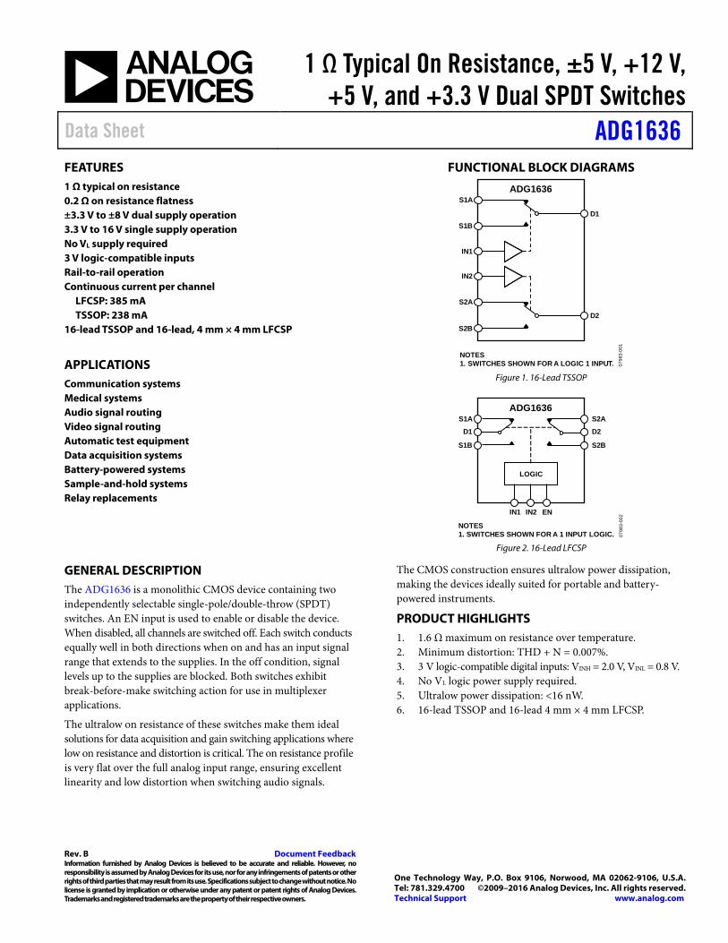
1 Ω Typical On Resistance, ±5 V, +12 V, +5 V, and +3.3 V Dual SPDT Switches Data Sheet ADG1636 Rev. B Document Feedback Information furnished by Analog Devices is believed to be accurate and reliable. However, no responsibility is assumed by Analog Devices for its use, nor for any infringements of patents or other rights of third parties that may result from its use. Specifications subject to change without notice. No license is granted by implication or otherwise under any patent or patent rights of Analog Devices. Trademarks and registered trademarks are the property of their respective owners. One Technology Way, P.O. Box 9106, Norwood, MA 02062-9106, U.S.A. Tel: 781.329.4700 ©2009–2016 Analog Devices, Inc. All rights reserved. Technical Support www.analog.com FEATURES 1 Ω typical on resistance 0.2 Ω on resistance flatness ±3.3 V to ±8 V dual supply operation 3.3 V to 16 V single supply operation No VL supply required 3 V logic-compatible inputs Rail-to-rail operation Continuous current per channel LFCSP: 385 mA TSSOP: 238 mA 16-lead TSSOP and 16-lead, 4 mm × 4 mm LFCSP APPLICATIONS Communication systems Medical systems Audio signal routing Video signal routing Automatic test equipment Data acquisition systems Battery-powered systems Sample-and-hold systems Relay replacements FUNCTIONAL BLOCK DIAGRAMS 07983-001 ADG1636 D1 D2 S2B S2A IN2 IN1 S1B S1A NOTES 1. SWITCHES SHOWN FOR A LOGIC 1 INPUT. Figure 1. 16-Lead TSSOP 07983-002 ADG1636 IN1 IN2 EN S1B D1 S1A S2B LOGIC D2 S2A NOTES 1. SWITCHES SHOWN FOR A 1 INPUT LOGIC. Figure 2. 16-Lead LFCSP GENERAL DESCRIPTION The ADG1636 is a monolithic CMOS device containing two independently selectable single-pole/double-throw (SPDT) switches. An EN input is used to enable or disable the device. When disabled, all channels are switched off. Each switch conducts equally well in both directions when on and has an input signal range that extends to the supplies. In the off condition, signal levels up to the supplies are blocked. Both switches exhibit break-before-make switching action for use in multiplexer applications. The ultralow on resistance of these switches make them ideal solutions for data acquisition and gain switching applications where low on resistance and distortion is critical. The on resistance profile is very flat over the full analog input range, ensuring excellent linearity and low distortion when switching audio signals. The CMOS construction ensures ultralow power dissipation, making the devices ideally suited for portable and battery- powered instruments. PRODUCT HIGHLIGHTS 1. 1.6 Ω maximum on resistance over temperature. 2. Minimum distortion: THD + N = 0.007%. 3. 3 V logic-compatible digital inputs: VINH = 2.0 V, VINL = 0.8 V. 4. No VL logic power supply required. 5. Ultralow power dissipation: <16 nW. 6. 16-lead TSSOP and 16-lead 4 mm × 4 mm LFCSP.
-
Upload
dangkhuong -
Category
Documents
-
view
230 -
download
0
Transcript of 1 Ω Typical On Resistance, ±5 V, +12 V, +5 V, and +3.3 V ... · 1 Ω Typical On Resistance, ±5...
1 Ω Typical On Resistance, ±5 V, +12 V, +5 V, and +3.3 V Dual SPDT Switches
Data Sheet ADG1636
Rev. B Document Feedback Information furnished by Analog Devices is believed to be accurate and reliable. However, no responsibility is assumed by Analog Devices for its use, nor for any infringements of patents or other rights of third parties that may result from its use. Specifications subject to change without notice. No license is granted by implication or otherwise under any patent or patent rights of Analog Devices. Trademarks and registered trademarks are the property of their respective owners.
One Technology Way, P.O. Box 9106, Norwood, MA 02062-9106, U.S.A.Tel: 781.329.4700 ©2009–2016 Analog Devices, Inc. All rights reserved. Technical Support www.analog.com
FEATURES 1 Ω typical on resistance 0.2 Ω on resistance flatness ±3.3 V to ±8 V dual supply operation 3.3 V to 16 V single supply operation No VL supply required 3 V logic-compatible inputs Rail-to-rail operation Continuous current per channel
LFCSP: 385 mA TSSOP: 238 mA
16-lead TSSOP and 16-lead, 4 mm × 4 mm LFCSP
APPLICATIONS Communication systems Medical systems Audio signal routing Video signal routing Automatic test equipment Data acquisition systems Battery-powered systems Sample-and-hold systems Relay replacements
FUNCTIONAL BLOCK DIAGRAMS
0798
3-00
1
ADG1636
D1
D2
S2B
S2A
IN2
IN1
S1B
S1A
NOTES1. SWITCHES SHOWN FOR A LOGIC 1 INPUT.
Figure 1. 16-Lead TSSOP
0798
3-00
2
ADG1636
IN1 IN2 EN
S1B
D1
S1A
S2B
LOGIC
D2
S2A
NOTES1. SWITCHES SHOWN FOR A 1 INPUT LOGIC.
Figure 2. 16-Lead LFCSP
GENERAL DESCRIPTION The ADG1636 is a monolithic CMOS device containing two independently selectable single-pole/double-throw (SPDT) switches. An EN input is used to enable or disable the device. When disabled, all channels are switched off. Each switch conducts equally well in both directions when on and has an input signal range that extends to the supplies. In the off condition, signal levels up to the supplies are blocked. Both switches exhibit break-before-make switching action for use in multiplexer applications.
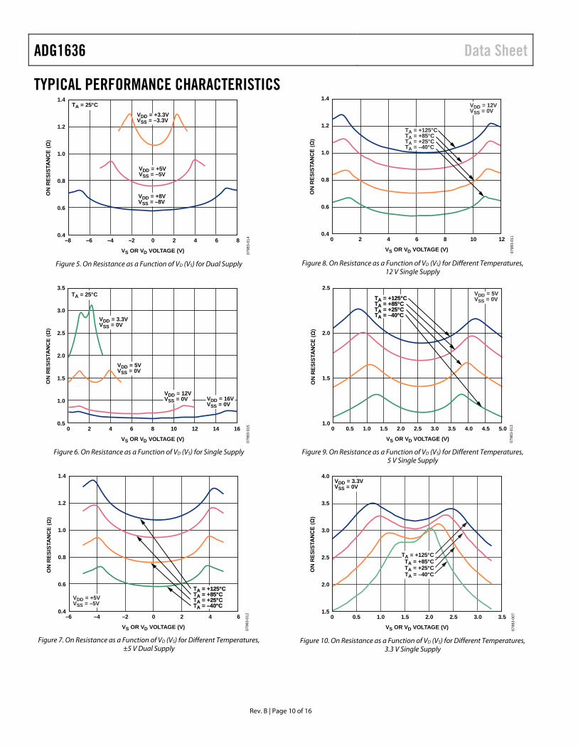
The ultralow on resistance of these switches make them ideal solutions for data acquisition and gain switching applications where low on resistance and distortion is critical. The on resistance profile is very flat over the full analog input range, ensuring excellent linearity and low distortion when switching audio signals.
The CMOS construction ensures ultralow power dissipation, making the devices ideally suited for portable and battery-powered instruments.
PRODUCT HIGHLIGHTS 1. 1.6 Ω maximum on resistance over temperature. 2. Minimum distortion: THD + N = 0.007%. 3. 3 V logic-compatible digital inputs: VINH = 2.0 V, VINL = 0.8 V. 4. No VL logic power supply required. 5. Ultralow power dissipation: <16 nW. 6. 16-lead TSSOP and 16-lead 4 mm × 4 mm LFCSP.

ADG1636 Data Sheet
Rev. B | Page 2 of 16
TABLE OF CONTENTS Features .............................................................................................. 1 Applications ....................................................................................... 1 General Description ......................................................................... 1 Functional Block Diagrams ............................................................. 1 Product Highlights ........................................................................... 1 Revision History ............................................................................... 2 Specifications ..................................................................................... 3
±5 V Dual Supply ......................................................................... 3 12 V Single Supply ........................................................................ 4 5 V Single Supply .......................................................................... 5
3.3 V Single Supply ........................................................................6 Continuous Current per Channel, S or D ..................................7
Absolute Maximum Ratings ............................................................8 ESD Caution...................................................................................8
Pin Configurations and Function Descriptions ............................9 Typical Performance Characteristics ........................................... 10 Test Circuits ..................................................................................... 13 Terminology .................................................................................... 15 Outline Dimensions ....................................................................... 16
Ordering Guide .......................................................................... 16
REVISION HISTORY 3/16—Rev. A to Rev. B Changed CP-16-13 to CP-16-26 .................................. Throughout Changes to Figure 3, Figure 4, and Table 7 ................................... 9 Updated Outline Dimensions ....................................................... 16 Changes to Ordering Guide .......................................................... 16 9/09—Rev. 0 to Rev. A Changes to Table 4 ............................................................................ 6 1/09—Revision 0: Initial Version

Data Sheet ADG1636
Rev. B | Page 3 of 16
SPECIFICATIONS ±5 V DUAL SUPPLY VDD = +5 V ± 10%, VSS = −5 V ± 10%, GND = 0 V, unless otherwise noted.
Table 1.
Parameter 25°C −40°C to +85°C
−40°C to +125°C Unit Test Conditions/Comments
ANALOG SWITCH Analog Signal Range VDD to VSS V On Resistance (RON) 1 Ω typ VS = ±4.5 V, IS = −10 mA; see Figure 23 1.2 1.4 1.6 Ω max VDD = ±4.5 V, VSS = ±4.5 V On Resistance Match Between Channels (∆RON) 0.04 Ω typ VS = ±4.5 V, IS = −10 mA
0.08 0.09 0.1 Ω max On Resistance Flatness (RFLAT(ON)) 0.2 Ω typ VS = ±4.5 V, IS = −10 mA
0.25 0.29 0.34 Ω max LEAKAGE CURRENTS VDD = +5.5 V, VSS = −5.5 V
Source Off Leakage, IS (Off ) ±0.1 nA typ VS = ±4.5 V, VD = ∓4.5 V; see Figure 24 ±0.25 ±1 ±4 nA max Drain Off Leakage, ID (Off ) ±0.1 nA typ VS = ±4.5V, VD = ∓4.5 V; see Figure 24 ±0.25 ±2 ±10 nA max Channel On Leakage, ID, IS (On) ±0.3 nA typ VS = VD = ±4.5 V; see Figure 25
±0.6 ±2 ±12 nA max DIGITAL INPUTS
Input High Voltage, VINH 2.0 V min Input Low Voltage, VINL 0.8 V max Input Current, IINL or IINH 0.005 µA typ VIN = VGND or VDD ±0.1 µA max Digital Input Capacitance, CIN 5 pF typ
DYNAMIC CHARACTERISTICS1 Transition Time, tTRANSITION 130 ns typ RL = 300 Ω, CL = 35 pF
209 245 273 ns max VS = 2.5 V; see Figure 30 tON (EN) 119 ns typ RL = 300 Ω, CL = 35 pF 148 166 176 ns max VS = 2.5 V; see Figure 30 tOFF (EN) 182 ns typ RL = 300 Ω, CL = 35 pF 228 259 281 ns max VS = 2.5 V; see Figure 30 Break-Before-Make Time Delay, tD 30 ns typ RL = 300 Ω, CL = 35 pF
17 ns min VS1 = VS2 = 2.5 V; see Figure 31 Charge Injection 130 pC typ VS = 0 V, RS = 0 Ω, CL = 1 nF; see Figure 32 Off Isolation 70 dB typ RL = 50 Ω, CL = 5 pF, f = 1 MHz; see Figure 26 Channel-to-Channel Crosstalk 90 dB typ RL = 50 Ω, CL = 5 pF, f = 1 MHz; see Figure 28 Total Harmonic Distortion + Noise (THD + N) 0.007 % typ RL = 110 Ω, 5 V p-p, f = 20 Hz to 20 kHz;
see Figure 29 −3 dB Bandwidth 25 MHz typ RL = 50 Ω, CL = 5 pF; see Figure 27 CS (Off ) 68 pF typ VS = 0 V, f = 1 MHz CD (Off ) 127 pF typ VS = 0 V, f = 1 MHz CD, CS (On) 220 pF typ VS = 0 V, f = 1 MHz
POWER REQUIREMENTS VDD = +5.5 V, VSS = −5.5 V IDD 0.001 µA typ Digital inputs = 0 V or VDD
1.0 µA max VDD/VSS ±3.3/±8 V min/max
1 Guaranteed by design, not subject to production test.

ADG1636 Data Sheet
Rev. B | Page 4 of 16
12 V SINGLE SUPPLY VDD = 12 V ± 10%, VSS = 0 V, GND = 0 V, unless otherwise noted.
Table 2.
Parameter 25°C −40°C to +85°C
−40°C to +125°C Unit Test Conditions/Comments
ANALOG SWITCH Analog Signal Range 0 V to VDD V On Resistance (RON) 0.95 Ω typ VS = 0 V to 10 V, IS = −10 mA; see Figure 23 1.1 1.25 1.45 Ω max VDD = 10.8 V, VSS = 0 V On Resistance Match Between Channels (∆RON) 0.03 Ω typ VS = 10 V, IS = −10 mA
0.06 0.07 0.08 Ω max On Resistance Flatness (RFLAT(ON)) 0.2 Ω typ VS = 0 V to 10 V, IS = −10 mA 0.23 0.27 0.32 Ω max
LEAKAGE CURRENTS VDD = 13.2 V, VSS = 0 V Source Off Leakage, IS (Off ) ±0.1 nA typ VS = 1 V/10 V, VS = 10 V/1 V; see Figure 24 ±0.25 ±1 ±4 nA max Drain Off Leakage, ID (Off ) ±0.1 nA typ VS = 1 V/10 V, VS = 10 V/1 V; see Figure 24 ±0.25 ±2 ±10 nA max Channel On Leakage, ID, IS (On) ±0.3 nA typ VS = VD = 1 V or 10 V; see Figure 25
±0.6 ±2 ±12 nA max DIGITAL INPUTS
Input High Voltage, VINH 2.0 V min Input Low Voltage, VINL 0.8 V max Input Current, IINL or IINH 0.001 µA typ VIN = VGND or VDD
±0.1 µA max Digital Input Capacitance, CIN 5 pF typ
DYNAMIC CHARACTERISTICS1 Transition Time, tTRANSITION 100 ns typ RL = 300 Ω, CL = 35 pF
153 183 206 ns max VS = 8 V; see Figure 30 tON (EN) 80 ns typ RL = 300 Ω, CL = 35 pF 95 103 110 ns max VS = 8 V; see Figure 30 tOFF (EN) 133 ns typ RL = 300 Ω, CL = 35 pF 161 187 210 ns max VS = 8 V; see Figure 30 Break-Before-Make Time Delay, tD 25 ns typ RL = 300 Ω, CL = 35 pF
17 ns min VS1 = VS2 = 8 V; see Figure 31 Charge Injection 150 pC typ VS = 6 V, RS = 0 Ω, CL = 1 nF; see Figure 32 Off Isolation 70 dB typ RL = 50 Ω, CL = 5 pF, f = 1 MHz; see Figure 26 Channel-to-Channel Crosstalk 90 dB typ RL = 50 Ω, CL = 5 pF, f = 1 MHz; see Figure 28 Total Harmonic Distortion + Noise (THD + N) 0.013 % typ RL = 110 Ω, 5 V p-p, f = 20 Hz to 20 kHz;
see Figure 29 −3 dB Bandwidth 27 MHz typ RL = 50 Ω, CL = 5 pF; see Figure 27 CS (Off ) 65 pF typ VS = 6 V, f = 1 MHz CD (Off ) 120 pF typ VS = 6 V, f = 1 MHz CD, CS (On) 216 pF typ VS = 6 V, f = 1 MHz
POWER REQUIREMENTS VDD = 12 V IDD 0.001 µA typ Digital inputs = 0 V or VDD 1 µA max IDD 230 µA typ Digital inputs = 5 V 360 µA max VDD 3.3/16 V min/max
1 Guaranteed by design, not subject to production test.
Data Sheet ADG1636
Rev. B | Page 5 of 16
5 V SINGLE SUPPLY VDD = 5 V ± 10%, VSS = 0 V, GND = 0 V, unless otherwise noted.
Table 3.
Parameter 25°C −40°C to +85°C
−40°C to 125°C Unit Test Conditions/Comments
ANALOG SWITCH Analog Signal Range 0 V to VDD V On Resistance (RON) 1.7 Ω typ VS = 0 V to 4.5 V, IS = −10 mA; see Figure 23 2.15 2.4 2.7 Ω max VDD = 4.5 V, VSS = 0 V On Resistance Match Between Channels (∆RON) 0.05 Ω typ VS = 0 V to 4.5 V, IS = −10 mA
0.09 0.12 0.15 Ω max On Resistance Flatness (RFLAT(ON)) 0.4 Ω typ VS = 0 V to 4.5 V, IS = −10 mA 0.53 0.55 0.6 Ω max
LEAKAGE CURRENTS VDD = 5.5 V, VSS = 0 V Source Off Leakage, IS (Off ) ±0.05 nA typ VS = 1 V/4.5 V, VD = 4.5 V/1 V; see Figure 24 ±0.25 ±1 ±4 nA max Drain Off Leakage, ID (Off ) ±0.05 nA typ VS = 1 V/4.5 V, VD = 4.5 V/1 V; see Figure 24 ±0.25 ±2 ±10 nA max Channel On Leakage, ID, IS (On) ±0.1 nA typ VS = VD = 1 V or 4.5 V; see Figure 25
±0.6 ±2 ±12 nA max DIGITAL INPUTS
Input High Voltage, VINH 2.0 V min Input Low Voltage, VINL 0.8 V max Input Current, IINL or IINH 0.001 µA typ VIN = VGND or VDD
±0.1 µA max Digital Input Capacitance, CIN 5 pF typ
DYNAMIC CHARACTERISTICS1 Transition Time, tTRANSITION 160 ns typ RL = 300 Ω, CL = 35 pF
271 319 355 ns max VS = 2.5 V; see Figure 30 tON (EN) 132 ns typ RL = 300 Ω, CL = 35 pF 172 185 201 ns max VS = 2.5 V; see Figure 30 tOFF (EN) 210 ns typ RL = 300 Ω, CL = 35 pF 268 313 345 ns max VS = 2.5 V; see Figure 30 Break-Before-Make Time Delay, tD 30 ns typ RL = 300 Ω, CL = 35 pF
17 ns min VS1 = VS2 = 2.5 V; see Figure 31 Charge Injection 70 pC typ VS = 2.5 V, RS = 0 Ω, CL = 1 nF; see Figure 32 Off Isolation 70 dB typ RL = 50 Ω, CL = 5 pF, f = 100 kHz;
see Figure 26 Channel-to-Channel Crosstalk 90 dB typ RL = 50 Ω, CL = 5 pF, f = 100 kHz;
see Figure 28 Total Harmonic Distortion + Noise (THD + N) 0.09 % typ RL = 110 Ω, f = 20 Hz to 20 kHz, VS = 3.5 V p-p;
see Figure 29 −3 dB Bandwidth 26 MHz typ RL = 50 Ω, CL = 5 pF; see Figure 27 CS (Off ) 76 pF typ VS = 2.5 V, f = 1 MHz CD (Off ) 145 pF typ VS = 2.5 V, f = 1 MHz CD, CS (On) 237 pF typ VS = 2.5 V, f = 1 MHz
POWER REQUIREMENTS VDD = 5.5 V IDD 0.001 µA typ Digital inputs = 0 V or VDD 1.0 1.0 µA max VDD 3.3/16 V min/max
1 Guaranteed by design, not subject to production test.

ADG1636 Data Sheet
Rev. B | Page 6 of 16
3.3 V SINGLE SUPPLY VDD = 3.3 V, VSS = 0 V, GND = 0 V, unless otherwise noted.
Table 4.
Parameter 25°C −40°C to +85°C
−40°C to +125°C Unit Test Conditions/Comments
ANALOG SWITCH Analog Signal Range 0 V to VDD V On Resistance (RON) 3.2 3.4 3.6 Ω typ VS = 0 V to VDD, IS = −10 mA; see Figure 23 VDD = 3.3 V, VSS = 0 V On Resistance Match Between Channels (∆RON) 0.06 0.07 0.08 Ω typ VS = 0 V to VDD, IS = −10 mA On Resistance Flatness (RFLAT(ON)) 1.2 1.3 1.4 Ω typ VS = 0 V to VDD, IS = −10 mA
LEAKAGE CURRENTS VDD = 3.6 V, VSS = 0 V Source Off Leakage, IS (Off ) ±0.02 nA typ VS = 0.6 V/3 V, VD = 3 V/0.6 V; see Figure 24 ±0.25 ±1 ±4 nA max Drain Off Leakage, ID (Off ) ±0.02 nA typ VS = 0.6 V/3 V, VD = 3 V/0.6 V; see Figure 24 ±0.25 ±2 ±10 nA max Channel On Leakage, ID, IS (On) ±0.05 nA typ VS = VD = 0.6 V or 3 V; see Figure 25
±0.6 ±2 ±12 nA max DIGITAL INPUTS
Input High Voltage, VINH 2.0 V min Input Low Voltage, VINL 0.8 V max Input Current, IINL or IINH 0.001 µA typ VIN = VGND or VDD
±0.1 µA max Digital Input Capacitance, CIN 5 pF typ
DYNAMIC CHARACTERISTICS1 Transition Time, tTRANSITION 275 ns typ RL = 300 Ω, CL = 35 pF
449 506 550 ns max VS = 1.5 V; see Figure 30 tON (EN) 225 ns typ RL = 300 Ω, CL = 35 pF 306 327 338 ns max VS = 1.5 V; see Figure 30 tOFF (EN) 340 ns typ RL = 300 Ω, CL = 35 pF 454 512 553 ns max VS = 1.5 V; see Figure 30 Break-Before-Make Time Delay, tD 50 ns typ RL = 300 Ω, CL = 35 pF
28 ns min VS1 = VS2 = 1.5 V; see Figure 31 Charge Injection 50 pC typ VS = 1.5 V, RS = 0 Ω, CL = 1 nF; see Figure 32 Off Isolation 70 dB typ RL = 50 Ω, CL = 5 pF, f = 100 kHz; see Figure 26 Channel-to-Channel Crosstalk 90 dB typ RL = 50 Ω, CL = 5 pF, f = 100 kHz;
see Figure 28 Total Harmonic Distortion + Noise (THD + N) 0.19 % typ RL = 33 Ω, f = 20 Hz to 20 kHz, VS = 2 V p-p;
see Figure 29 −3 dB Bandwidth 26 MHz typ RL = 50 Ω, CL = 5 pF; see Figure 27 CS (Off ) 80 pF typ VS = 1.5 V, f = 1 MHz CD (Off ) 153 pF typ VS = 1.5 V, f = 1 MHz CD, CS (On) 243 pF typ VS = 1.5 V, f = 1 MHz
POWER REQUIREMENTS VDD = 3.6 V IDD 0.001 µA typ Digital inputs = 0 V or VDD 1.0 1.0 µA max VDD 3.3/16 V min/max
1 Guaranteed by design, not subject to production test.

Data Sheet ADG1636
Rev. B | Page 7 of 16
CONTINUOUS CURRENT PER CHANNEL, S OR D
Table 5. Parameter 25°C 85°C 125°C Unit
CONTINUOUS CURRENT, S OR D VDD = +5 V, VSS = −5 V
TSSOP (θJA = 150.4°C/W) 238 151 88 mA maximum LFCSP (θJA = 48.7°C/W) 385 220 105 mA maximum
VDD = 12 V, VSS = 0 V TSSOP (θJA = 150.4°C/W) 280 175 98 mA maximum LFCSP (θJA = 48.7°C/W) 469 259 119 mA maximum
VDD = 5 V, VSS = 0 V TSSOP (θJA = 150.4°C/W) 189 126 77 mA maximum LFCSP (θJA = 48.7°C/W) 301 182 98 mA maximum
VDD = 3.3 V, VSS = 0 V TSSOP (θJA = 150.4°C/W) 189 130 84 mA maximum LFCSP (θJA = 48.7°C/W) 305 189 105 mA maximum

ADG1636 Data Sheet
Rev. B | Page 8 of 16
ABSOLUTE MAXIMUM RATINGS TA = 25°C, unless otherwise noted.
Table 6. Parameter Rating VDD to VSS 18 V VDD to GND −0.3 V to +18 V VSS to GND +0.3 V to −18 V Analog Inputs1 VSS − 0.3 V to VDD + 0.3 V or
30 mA, whichever occurs first Digital Inputs1 GND − 0.3 V to VDD + 0.3 V or
30 mA, whichever occurs first Peak Current, S or D 850 mA (pulsed at 1 ms,
10% duty cycle maximum) Continuous Current, S or D2 Data + 15% Operating Temperature Range
Industrial (Y Version) −40°C to +125°C Storage Temperature Range −65°C to +150°C Junction Temperature 150°C θJA Thermal Impedance
16-Lead TSSOP (2-Layer Board) 150.4°C/W 16-Lead LFCSP (4-Layer Board) 48.7°C/W
Reflow Soldering Peak Temperature, Pb free
260°C
1 Overvoltages at IN, S, or D are clamped by internal diodes. Current should be
limited to the maximum ratings given. 2 See Table 5.
Stresses at or above those listed under Absolute Maximum Ratings may cause permanent damage to the product. This is a stress rating only; functional operation of the product at these or any other conditions above those indicated in the operational section of this specification is not implied. Operation beyond the maximum operating conditions for extended periods may affect product reliability.
ESD CAUTION

Data Sheet ADG1636
Rev. B | Page 9 of 16
PIN CONFIGURATIONS AND FUNCTION DESCRIPTIONS
NOTES1. NIC = NO INTERNAL CONNECTION.
1
2
3
4
5
6
7
8
S1A
D1
S1B
NIC
GND
VSS
IN1
NIC
16
15
14
13
12
11
10
9
NIC
EN
VDD
S2A
IN2
D2
S2B
NIC
ADG1636TOP VIEW
(Not to Scale)
0798
3-00
3
Figure 3. 16-Lead TSSOP Pin Configuration
0798
3-00
4NOTES1. NIC = NO INTERNAL CONNECTION.2. TIE THE EXPOSED PAD TO THE SUBSTRATE, VSS.
12
11
10
1
3
4 9
2
65 7 8
16 15 14 13
D1
S1B
VSS
GND
EN
NIC
NIC
IN1
S1A
VDD
S2B
D2
NIC IN2
NIC
S2A
TOP VIEW(Not to Scale)
ADG1636
Figure 4. 16-Lead LFCSP Pin Configuration
Table 7. Pin Function Descriptions Pin No.
Mnemonic Description TSSOP LFCSP 1 15 IN1 Logic Control Input. 2 16 S1A Source Terminal. This pin can be an input or output. 3 1 D1 Drain Terminal. This pin can be an input or output. 4 2 S1B Source Terminal. This pin can be an input or output. 5 3 VSS Most Negative Power Supply Potential. 6 4 GND Ground (0 V) Reference. 7, 8, 15, 16 5, 7, 13, 14 NIC No Internal Connection. 9 6 IN2 Logic Control Input. 10 8 S2A Source Terminal. This pin can be an input or output. 11 9 D2 Drain Terminal. This pin can be an input or output. 12 10 S2B Source Terminal. This pin can be an input or output. 13 11 VDD Most Positive Power Supply Potential. 14 12 EN Active High Digital Input. When this pin is low, the device is disabled and all switches are
off. When this pin is high, the Ax logic inputs determine the on switches. N/A1 0 EPAD Exposed Pad. Tie the exposed pad to the substrate, VSS. 1 N/A means not applicable.
Table 8. ADG1636 TSSOP Truth Table EN INx SxA SxB 0 X Off Off 1 0 Off On 1 1 On Off
Table 9. ADG1636 LFCSP Truth Table EN INx SxA SxB 0 X Off Off 1 0 Off On 1 1 On Off
ADG1636 Data Sheet
Rev. B | Page 10 of 16
TYPICAL PERFORMANCE CHARACTERISTICS
0.4
0.6
0.8
1.0
1.2
1.4
–8 –6 –4 –2 0 2 4 6 8
ON
RES
ISTA
NC
E (Ω
)
VS OR VD VOLTAGE (V)
TA = 25°CVDD = +3.3VVSS = –3.3V
VDD = +5VVSS = –5V
VDD = +8VVSS = –8V
0798
3-01
4
Figure 5. On Resistance as a Function of VD (VS) for Dual Supply
0.5
1.0
1.5
2.0
2.5
3.0
3.5
0 2 4 6 8 10 12 14 16
ON
RES
ISTA
NC
E (Ω
)
VS OR VD VOLTAGE (V)
VDD = 3.3VVSS = 0V
VDD = 12VVSS = 0V
VDD = 5VVSS = 0V
VDD = 16VVSS = 0V
TA = 25°C
0798
3-01
5
Figure 6. On Resistance as a Function of VD (VS) for Single Supply
0.4
0.6
0.8
1.0
1.2
1.4
–6 –4 –2 0 2 4 6
ON
RES
ISTA
NC
E (Ω
)
VS OR VD VOLTAGE (V)
TA = +125°CTA = +85°CTA = +25°CTA = –40°C
TA = +125°CTA = +85°CTA = +25°CTA = –40°C
VDD = +5VVSS = –5V
0798
3-01
2
Figure 7. On Resistance as a Function of VD (VS) for Different Temperatures,
±5 V Dual Supply
0.4
0.6
0.8
1.0
1.2
1.4
0 2 4 6 8 10 12
ON
RES
ISTA
NC
E (Ω
)
VS OR VD VOLTAGE (V)
VDD = 12VVSS = 0V
0798
3-01
1
TA = +125°CTA = +85°CTA = +25°CTA = –40°C
Figure 8. On Resistance as a Function of VD (VS) for Different Temperatures,
12 V Single Supply
1.0
1.5
2.0
2.5
0 0.5 1.0 1.5 2.0 2.5 3.0 3.5 4.0 4.5 5.0
ON
RES
ISTA
NC
E (Ω
)
VS OR VD VOLTAGE (V)
TA = +125°CTA = +85°CTA = +25°CTA = –40°C
TA = +125°CTA = +85°CTA = +25°CTA = –40°C
VDD = 5VVSS = 0V
0798
3-01
3
Figure 9. On Resistance as a Function of VD (VS) for Different Temperatures,
5 V Single Supply
1.5
2.0
2.5
3.0
3.5
4.0
0 0.5 1.0 1.5 2.0 2.5 3.0 3.5
ON
RES
ISTA
NC
E (Ω
)
VS OR VD VOLTAGE (V)
VDD = 3.3VVSS = 0V
TA = –40°CTA = +25°CTA = +85°C
TA = +125°C
0798
3-00
7
Figure 10. On Resistance as a Function of VD (VS) for Different Temperatures,
3.3 V Single Supply

Data Sheet ADG1636
Rev. B | Page 11 of 16
TEMPERATURE (°C)
–15
–10
–5
0
5
10
15
LEA
KA
GE
CU
RR
ENT
(nA
)
0 20 40 60 80 100 120
ID (OFF) +, –
ID, IS (ON) +, +
ID (OFF) –, +
IS (OFF) +, –
IS (OFF) –, +
ID, IS (ON) –, –
0798
3-03
3
Figure 11. Leakage Currents as a Function of Temperature, ±5 V Dual Supply
07
983-
032
TEMPERATURE (°C)
LEA
KA
GE
CU
RR
ENT
(nA
)
0 20 40 60 80 100 120
ID (OFF) +, –
ID, IS (ON) +, +
ID (OFF) –, +
IS (OFF) +, –
IS (OFF) –, +ID, IS (ON) –, –
–15
–10
–5
0
5
10
15
20
Figure 12. Leakage Currents as a Function of Temperature, 12 V Single Supply
–5
0
5
10
15
20
0 20 40 60 80 100 120
LEA
KA
GE
CU
RR
ENT
(nA
)
TEMPERATURE (°C)
ID, IS (OFF) +, +
ID, IS (OFF) –, –
ID (OFF) –, +
IS (OFF) +, –
ID (OFF) +, –IS (OFF) –, +
0798
3-03
0
Figure 13. Leakage Currents as a Function of Temperature,
5 V Single Supply
0 20 40 60 80 100 120
TEMPERATURE (°C)
ID, IS (OFF) +, +
ID, IS (OFF) –, –
ID (OFF) –, +
IS (OFF) +, –
ID (OFF) +, –
IS (OFF) –, +
–4
–2
0
2
4
6
8
10
12
14
16
18
LEA
KA
GE
CU
RR
ENT
(nA
)
0798
3-03
1
Figure 14. Leakage Currents as a Function of Temperature,
3.3 V Single Supply
–100
0
100
200
300
400
500
600
I DD
(µA
)
0 2 4 6 8 10 12 14
LOGIC (V)
IDD PER CHANNELTA = 25°C
IDD = +12VISS = 0V
IDD = +5VISS = –5V
IDD = +5VISS = 0V
IDD = +3.3VISS = 0V
0798
3-00
6
Figure 15. IDD vs. Logic Level
0
50
100
150
200
250
300
–6 –4 –2 0 2 4 6 8 10 12 14
CH
AR
GE
INJE
CTI
ON
(pC
)
VS (V)
VDD = +12VVSS = 0V
VDD = +5VVSS = 0V
VDD = +3.3VVSS = 0V
VDD = +5VVSS = –5V
0798
3-01
0
Figure 16. Charge Injection vs. Source Voltage
ADG1636 Data Sheet
Rev. B | Page 12 of 16
50
100
150
200
250
300
350
400
450
–40 –20 0 20 40 60 80 100 120
TIM
E (n
s)
TEMPERATURE (°C) 0798
3-01
9
VDD = +3.3V, VSS = 0V
VDD = +5V, VSS = 0V
VDD = +5V, VSS = –5V
VDD = +12V, VSS = 0V
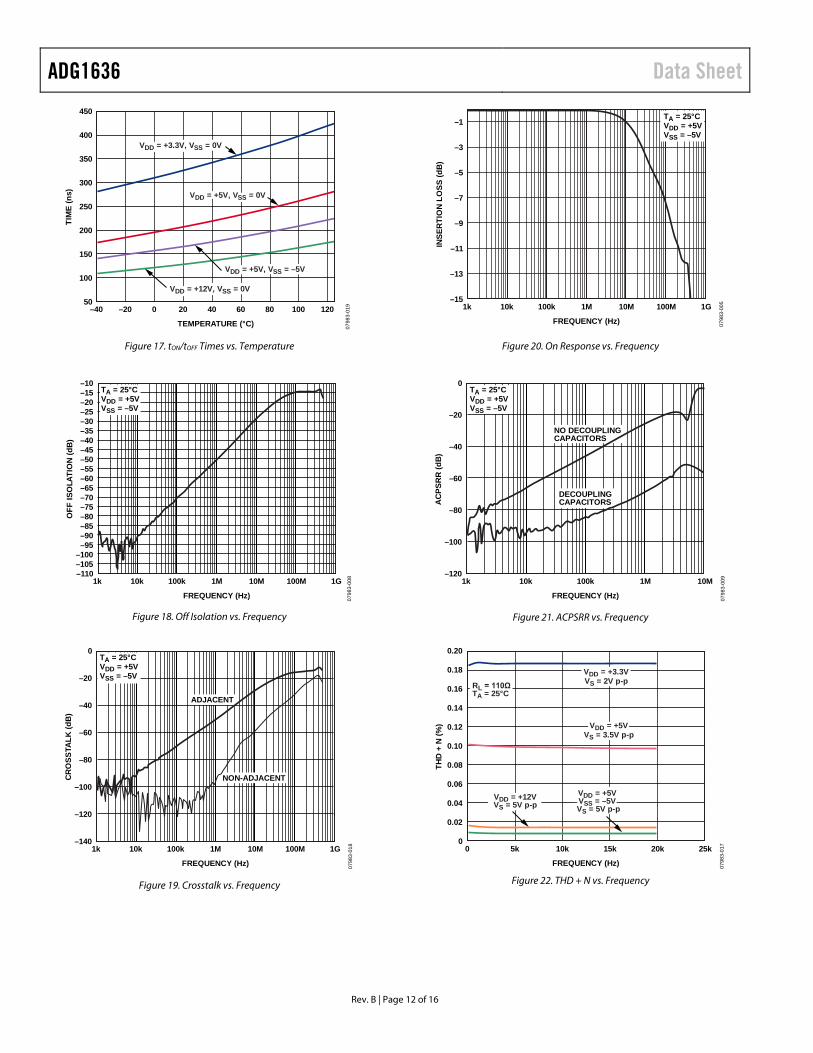
Figure 17. tON/tOFF Times vs. Temperature 07
983-
008–110
–105–100
–95–90–85–80–75–70–65–60–55–50–45–40–35–30–25–20–15–10
OFF
ISO
LATI
ON
(dB
)
FREQUENCY (Hz)
100k 1M 10M 100M 1G10k1k
TA = 25°CVDD = +5VVSS = –5V
Figure 18. Off Isolation vs. Frequency
–140
–120
–100
–80
–60
–40
–20
0
CR
OSS
TALK
(dB
)
FREQUENCY (Hz)
100k 1M 10M 100M 1G10k1k
0798
3-01
8
TA = 25°CVDD = +5VVSS = –5V
ADJACENT
NON-ADJACENT
Figure 19. Crosstalk vs. Frequency
INSE
RTI
ON
LO
SS (d
B)
FREQUENCY (Hz)
100k 1M 10M 100M 1G10k1k–15
–13
–11
–9
–7
–5
–3
–1TA = 25°CVDD = +5VVSS = –5V
0798
3-00
5
Figure 20. On Response vs. Frequency
–120
–100
–80
–60
–40
–20
0
FREQUENCY (Hz)
100k 1M 10M10k1k
TA = 25°CVDD = +5VVSS = –5V
AC
PSR
R (d
B)
0798
3-00
9
NO DECOUPLINGCAPACITORS
DECOUPLINGCAPACITORS
Figure 21. ACPSRR vs. Frequency
00
0.02
0.04
0.06
0.08
0.10
0.12
0.14
0.16
0.18
0.20
THD
+ N
(%)
FREQUENCY (Hz)
15k 20k10k5k 25k
VDD = +3.3VVS = 2V p-p
VDD = +5VVS = 3.5V p-p
VDD = +5VVSS = –5VVS = 5V p-p
VDD = +12VVS = 5V p-p
0798
3-01
7
RL = 110ΩTA = 25°C
Figure 22. THD + N vs. Frequency
Data Sheet ADG1636
Rev. B | Page 13 of 16
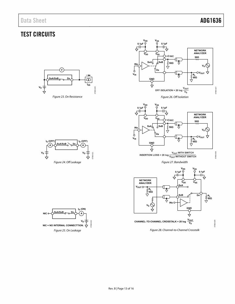
TEST CIRCUITS
IDS
SxA/SxB Dx
VS
V
0798
3-02
0Figure 23. On Resistance
SxA/SxB Dx
VS
A A
VD
IS (OFF) ID (OFF)
0798
3-02
1
Figure 24. Off Leakage
SxA/SxB DxA
VD
ID (ON)
NIC
NIC = NO INTERNAL CONNECTTION.
0798
3-02
2
Figure 25. On Leakage
VOUT
50Ω
NETWORKANALYZER
RL50Ω
INx
VIN
SxA
Dx
VS
VDD VSS
0.1µF
VDD
0.1µF
VSS
GND
50Ω
NIC
SxB
OFF ISOLATION = 20 logVOUT
VS 0798
3-02
7
Figure 26. Off Isolation
VOUT
50Ω
NETWORKANALYZER
RL50Ω
INx
VIN
SxA
Dx
VS
VDD VSS
0.1µF
VDD
0.1µF
VSS
GND
50Ω
NIC
SxB
INSERTION LOSS = 20 logVOUT WITH SWITCH
VOUT WITHOUT SWITCH
0798
3-02
8
Figure 27. Bandwidth
CHANNEL-TO-CHANNEL CROSSTALK = 20 logVOUT
GND
SxA
DxSxB
VOUT
NETWORKANALYZER
RL50Ω
RL50Ω
VS
VS
VDD VSS
0.1µF
VDD
0.1µF
VSS
INx
0798
3-02
9
Figure 28. Channel-to-Channel Crosstalk
ADG1636 Data Sheet
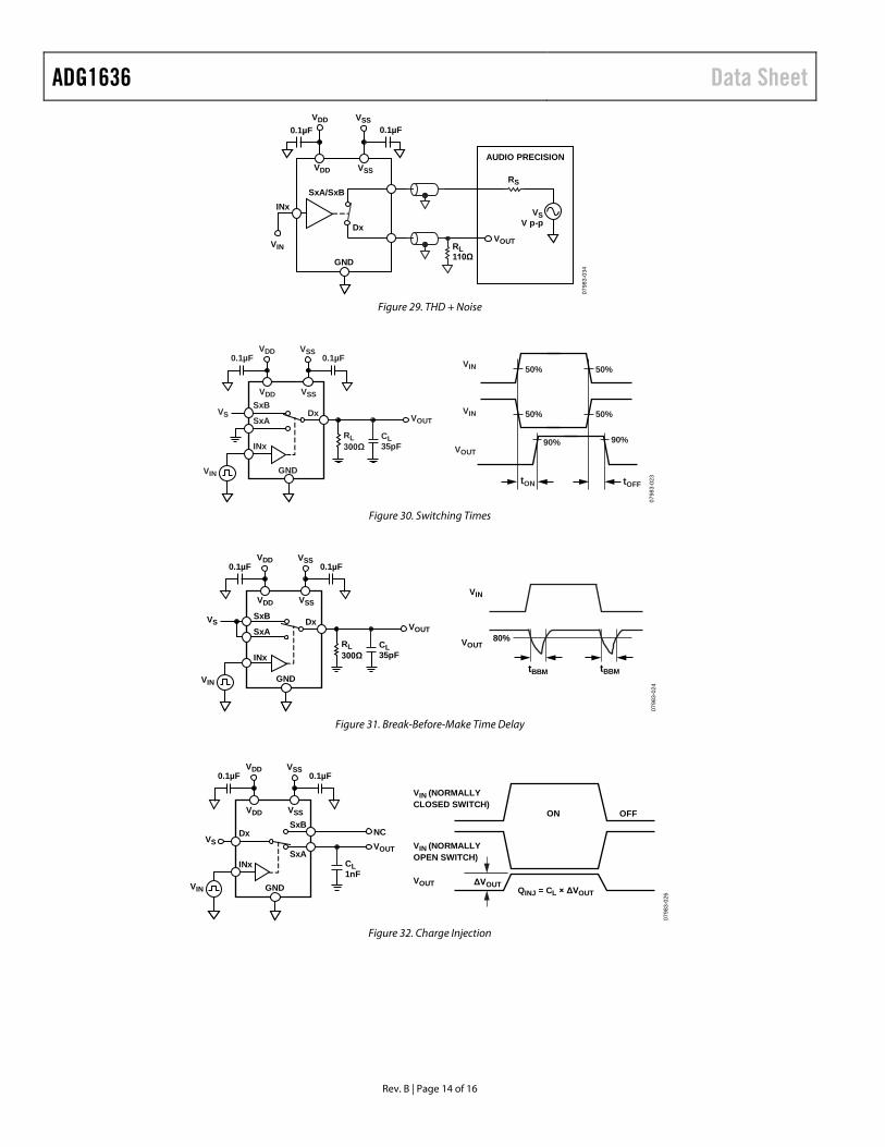
Rev. B | Page 14 of 16
VOUT
RS
AUDIO PRECISION
RL110Ω
INx
VIN
SxA/SxB
DxVS
V p-p
VDD VSS
0.1µFVDD
0.1µFVSS
GND
0798
3-03
4
Figure 29. THD + Noise
INx
VOUTDx
SxA
VDD VSS
VDD VSS
GND
CL35pF
SxB
VIN
VS
0.1µF0.1µF
RL300Ω
50%
50%
90%
50%
50%
90%
tON tOFF
VIN
VOUT
VIN
0798
3-02
3
Figure 30. Switching Times
INx
VOUTDx
SxA
VDD VSS
VDD VSS
GND
CL35pF
SxB
VIN
VS
0.1µF0.1µF
RL300Ω
80%
tBBM tBBM
VOUT
VIN
0798
3-02
4
Figure 31. Break-Before-Make Time Delay
VIN (NORMALLYCLOSED SWITCH)
VOUT
VIN (NORMALLYOPEN SWITCH)
OFF
ΔVOUT
ON
QINJ = CL × ΔVOUT
INx
VOUT
Dx
SxA
VDD VSS
VDD VSS
GND
CL1nF
NCSxB
VIN
VS
0.1µF0.1µF
0798
3-02
6
Figure 32. Charge Injection
Data Sheet ADG1636
Rev. B | Page 15 of 16
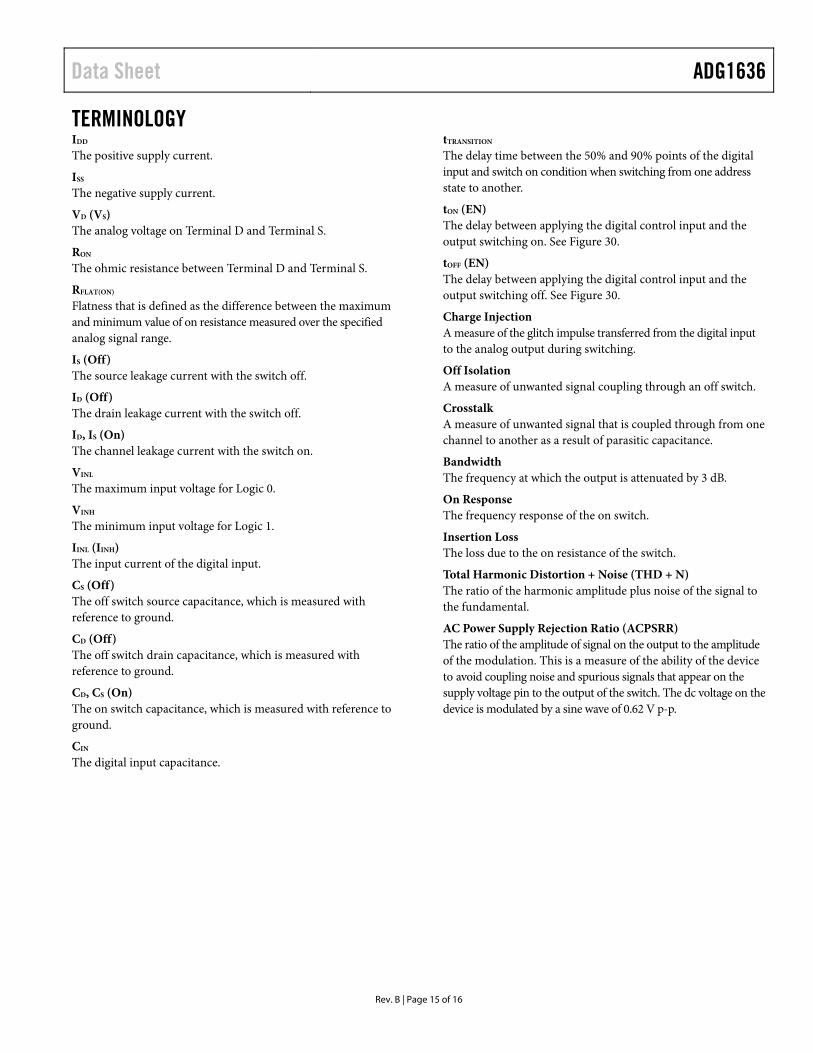
TERMINOLOGY IDD The positive supply current.
ISS The negative supply current.
VD (VS) The analog voltage on Terminal D and Terminal S.
RON The ohmic resistance between Terminal D and Terminal S.
RFLAT(ON)
Flatness that is defined as the difference between the maximum and minimum value of on resistance measured over the specified analog signal range.
IS (Off) The source leakage current with the switch off.
ID (Off) The drain leakage current with the switch off.
ID, IS (On) The channel leakage current with the switch on.
VINL The maximum input voltage for Logic 0.
VINH The minimum input voltage for Logic 1.
IINL (IINH) The input current of the digital input.
CS (Off) The off switch source capacitance, which is measured with reference to ground.
CD (Off) The off switch drain capacitance, which is measured with reference to ground.
CD, CS (On) The on switch capacitance, which is measured with reference to ground.
CIN The digital input capacitance.
tTRANSITION The delay time between the 50% and 90% points of the digital input and switch on condition when switching from one address state to another.
tON (EN) The delay between applying the digital control input and the output switching on. See Figure 30.
tOFF (EN) The delay between applying the digital control input and the output switching off. See Figure 30.
Charge Injection A measure of the glitch impulse transferred from the digital input to the analog output during switching.
Off Isolation A measure of unwanted signal coupling through an off switch.
Crosstalk A measure of unwanted signal that is coupled through from one channel to another as a result of parasitic capacitance.
Bandwidth The frequency at which the output is attenuated by 3 dB.
On Response The frequency response of the on switch.
Insertion Loss The loss due to the on resistance of the switch.
Total Harmonic Distortion + Noise (THD + N) The ratio of the harmonic amplitude plus noise of the signal to the fundamental.
AC Power Supply Rejection Ratio (ACPSRR) The ratio of the amplitude of signal on the output to the amplitude of the modulation. This is a measure of the ability of the device to avoid coupling noise and spurious signals that appear on the supply voltage pin to the output of the switch. The dc voltage on the device is modulated by a sine wave of 0.62 V p-p.

ADG1636 Data Sheet
Rev. B | Page 16 of 16
OUTLINE DIMENSIONS
16 9
81
PIN 1
SEATINGPLANE
8°0°
4.504.404.30
6.40BSC
5.105.004.90
0.65BSC
0.150.05
1.20MAX
0.200.09 0.75
0.600.45
0.300.19
COPLANARITY0.10
COMPLIANT TO JEDEC STANDARDS MO-153-AB Figure 33. 16-Lead Thin Shrink Small Outline Package [TSSOP]
(RU-16) Dimensions shown in millimeters
COMPLIANT TO JEDEC STANDARDS MO-220-WGGC. 0427
09-A
10.65BSC
BOTTOM VIEWTOP VIEW
16
589
1213
4
EXPOSEDPAD
PIN 1INDICATOR
4.104.00 SQ3.90
0.500.400.30
SEATINGPLANE
0.800.750.70 0.05 MAX
0.02 NOM
0.20 REF
COPLANARITY0.08
PIN 1INDICATOR
0.350.300.25
2.602.50 SQ2.40
FOR PROPER CONNECTION OFTHE EXPOSED PAD, REFER TOTHE PIN CONFIGURATION ANDFUNCTION DESCRIPTIONSSECTION OF THIS DATA SHEET.
Figure 34. 16-Lead Lead Frame Chip Scale Package [LFCSP]
4 mm × 4 mm Body and 0.75 mm Package Height (CP-16-26)
Dimensions shown in millimeters
ORDERING GUIDE Model1 Temperature Range Package Description Package Option ADG1636BRUZ −40°C to +125°C 16-Lead Thin Shrink Small Outline Package [TSSOP] RU-16 ADG1636BRUZ-REEL −40°C to +125°C 16-Lead Thin Shrink Small Outline Package [TSSOP] RU-16 ADG1636BRUZ-REEL7 −40°C to +125°C 16-Lead Thin Shrink Small Outline Package [TSSOP] RU-16 ADG1636BCPZ-REEL −40°C to +125°C 16-Lead Lead Frame Chip Scale Package [LFCSP] CP-16-26 ADG1636BCPZ-REEL7 −40°C to +125°C 16-Lead Lead Frame Chip Scale Package [LFCSP] CP-16-26 1 Z = RoHS Compliant Part.
©2009–2016 Analog Devices, Inc. All rights reserved. Trademarks and registered trademarks are the property of their respective owners. D07983-0-3/16(B)