1. SDRAM Controller Core - Purdue Engineering. SDRAM Controller Core ... The SDRAM controller core...
22
Altera Corporation 1–1 October 2007 Altera Corporation 1–1 October 2007 1. SDRAM Controller Core Core Overview The SDRAM controller core with Avalon ® interface provides an Avalon Memory-Mapped (Avalon-MM) interface to off-chip SDRAM. The SDRAM controller allows designers to create custom systems in an Altera ® FPGA that connect easily to SDRAM chips. The SDRAM controller supports standard SDRAM as described in the PC100 specification. SDRAM is commonly used in cost-sensitive applications requiring large amounts of volatile memory. While SDRAM is relatively inexpensive, control logic is required to perform refresh operations, open-row management, and other delays and command sequences. The SDRAM controller connects to one or more SDRAM chips, and handles all SDRAM protocol requirements. Internal to the FPGA, the core presents an Avalon-MM slave port that appears as linear memory (that is, flat address space) to Avalon-MM master peripherals. The core can access SDRAM subsystems with various data widths (8, 16, 32, or 64 bits), various memory sizes, and multiple chip selects. The Avalon-MM interface is latency-aware, allowing read transfers to be pipelined. The core can optionally share its address and data buses with other off-chip Avalon-MM tri-state devices. This feature is valuable in systems that have limited I/O pins, yet must connect to multiple memory chips in addition to SDRAM. The SDRAM controller core with Avalon interface is SOPC Builder-ready and integrates easily into any SOPC Builder-generated system. This chapter contains the following sections: ■ “Functional Description” on page 1–2 ■ “Device and Tools Support” on page 1–6 ■ “Instantiating the Core in SOPC Builder” on page 1–6 ■ “Hardware Simulation Considerations” on page 1–9 ■ “Software Programming Model” on page 1–13 ■ “Clock, PLL and Timing Considerations” on page 1–13 NII51005-7.2.0
Transcript of 1. SDRAM Controller Core - Purdue Engineering. SDRAM Controller Core ... The SDRAM controller core...

Altera Corporation 1–1October 2007 Altera Corporation 1–1October 2007
1. SDRAM Controller Core
Core Overview The SDRAM controller core with Avalon® interface provides an Avalon Memory-Mapped (Avalon-MM) interface to off-chip SDRAM. The SDRAM controller allows designers to create custom systems in an Altera® FPGA that connect easily to SDRAM chips. The SDRAM controller supports standard SDRAM as described in the PC100 specification.
SDRAM is commonly used in cost-sensitive applications requiring large amounts of volatile memory. While SDRAM is relatively inexpensive, control logic is required to perform refresh operations, open-row management, and other delays and command sequences. The SDRAM controller connects to one or more SDRAM chips, and handles all SDRAM protocol requirements. Internal to the FPGA, the core presents an Avalon-MM slave port that appears as linear memory (that is, flat address space) to Avalon-MM master peripherals.
The core can access SDRAM subsystems with various data widths (8, 16, 32, or 64 bits), various memory sizes, and multiple chip selects. The Avalon-MM interface is latency-aware, allowing read transfers to be pipelined. The core can optionally share its address and data buses with other off-chip Avalon-MM tri-state devices. This feature is valuable in systems that have limited I/O pins, yet must connect to multiple memory chips in addition to SDRAM.
The SDRAM controller core with Avalon interface is SOPC Builder-ready and integrates easily into any SOPC Builder-generated system. This chapter contains the following sections:
■ “Functional Description” on page 1–2■ “Device and Tools Support” on page 1–6■ “Instantiating the Core in SOPC Builder” on page 1–6■ “Hardware Simulation Considerations” on page 1–9■ “Software Programming Model” on page 1–13■ “Clock, PLL and Timing Considerations” on page 1–13
NII51005-7.2.0
1–2 Altera Corporation October 2007
Quartus II Handbook, Volume 5
1–2 Altera CorporationOctober 2007
Quartus II Handbook, Volume 5
Functional Description
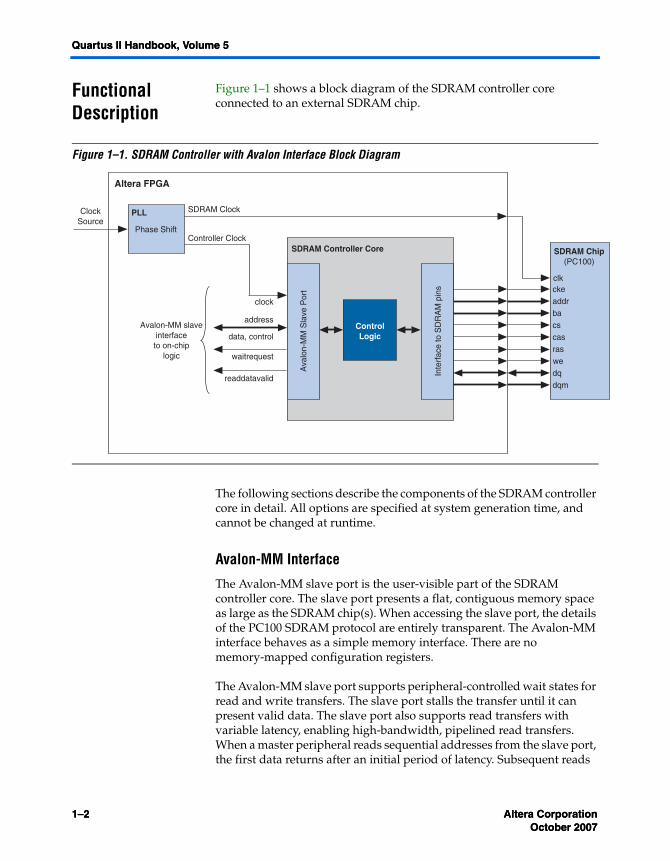
Figure 1–1 shows a block diagram of the SDRAM controller core connected to an external SDRAM chip.
Figure 1–1. SDRAM Controller with Avalon Interface Block Diagram
The following sections describe the components of the SDRAM controller core in detail. All options are specified at system generation time, and cannot be changed at runtime.
Avalon-MM Interface
The Avalon-MM slave port is the user-visible part of the SDRAM controller core. The slave port presents a flat, contiguous memory space as large as the SDRAM chip(s). When accessing the slave port, the details of the PC100 SDRAM protocol are entirely transparent. The Avalon-MM interface behaves as a simple memory interface. There are no memory-mapped configuration registers.
The Avalon-MM slave port supports peripheral-controlled wait states for read and write transfers. The slave port stalls the transfer until it can present valid data. The slave port also supports read transfers with variable latency, enabling high-bandwidth, pipelined read transfers. When a master peripheral reads sequential addresses from the slave port, the first data returns after an initial period of latency. Subsequent reads
Avalon-MM slaveinterfaceto on-chip
logic
SDRAM Controller Core
data, control
Ava
lon-
MM
Sla
ve P
ort
clock
waitrequest
readdatavaliddqdqm
PLL
Phase Shift
Inte
rfac
e to
SD
RA
M p
ins
Altera FPGA
clk
addr
rascascs
cke
ba
we
ControlLogic
address
SDRAM Clock
Controller Clock
ClockSource
SDRAM Chip(PC100)

Altera Corporation 1–3October 2007
Functional Description
Altera Corporation 1–3October 2007
Functional Description
can produce new data every clock cycle. However, data is not guaranteed to return every clock cycle, because the SDRAM controller must pause periodically to refresh the SDRAM.
f For details about Avalon-MM transfer types, refer to the Avalon Memory-Mapped Interface Specification.
Off-Chip SDRAM Interface
The interface to the external SDRAM chip presents the signals defined by the PC100 standard. These signals must be connected externally to the SDRAM chip(s) through I/O pins on the Altera FPGA.
Signal Timing and Electrical Characteristics
The timing and sequencing of signals depends on the configuration of the core. The hardware designer configures the core to match the SDRAM chip chosen for the system. See “Instantiating the Core in SOPC Builder” on page 1–6 for details. The electrical characteristics of the FPGA pins depend on both the target device family and the assignments made in the Quartus® II software. Some FPGA families support a wider range of electrical standards, and therefore are capable of interfacing with a greater variety of SDRAM chips. For details, see the handbook for the target FPGA family.
Synchronizing Clock and Data Signals
The clock for the SDRAM chip (hereafter "SDRAM clock") must be driven at the same frequency as the clock for the Avalon-MM interface on the SDRAM controller (hereafter "controller clock"). As in all synchronous design, you must ensure that address, data, and control signals at the SDRAM pins are stable when a clock edge arrives. As shown in Figure 1–1, you can use an on-chip phase-locked loop (PLL) to alleviate clock skew between the SDRAM controller core and the SDRAM chip. At lower clock speeds, the PLL might not be necessary. At higher clock rates, a PLL is necessary to ensure that the SDRAM clock toggles only when signals are stable on the pins. The PLL block is not part of the SDRAM controller core. If a PLL is necessary, you must instantiate it manually. You can instantiate the PLL core interface, which is an SOPC Builder component, or instantiate an altpll megafunction outside the SOPC Builder system module.
If you use a PLL, you must tune the PLL to introduce a clock phase shift so that SDRAM clock edges arrive after synchronous signals have stabilized. See “Clock, PLL and Timing Considerations” on page 1–13 for details.

1–4 Altera Corporation October 2007
Quartus II Handbook, Volume 5
1–4 Altera CorporationOctober 2007
Quartus II Handbook, Volume 5
f For more information about instantiating a PLL in your SOPC Builder system, refer to the PLL Core chapter in volume 5 of the Quartus II Handbook. The Nios® II development tools provide example hardware designs that use the SDRAM controller core in conjunction with a PLL, which you can use as a reference for your custom designs. The Nios II development tools are available free for download from www.altera.com.
Clock Enable (CKE) Not Supported
The SDRAM controller does not support clock-disable modes. The SDRAM controller permanently asserts the CKE signal on the SDRAM.
Sharing Pins with Other Avalon-MM Tri-State Devices
If an Avalon-MM tri-state bridge is present in the SOPC Builder system, the SDRAM controller core can share pins with the existing tri-state bridge. In this case, the core’s addr, dq (data) and dqm (byte-enable) pins are shared with other devices connected to the Avalon-MM tri-state bridge. This feature conserves I/O pins, which is valuable in systems that have multiple external memory chips (for example, flash, SRAM, and SDRAM), but too few pins to dedicate to the SDRAM chip. See “Performance Considerations” for details about how pin sharing affects performance.
1 The SDRAM addresses must connect all address bits regardless of the size of the word so that the low-order address bits on the tri-state bridge align with the low-order address bits on the memory device. It is not possible to drop A0 for memories when the smallest access size is 16 bits or A0-A1 when the smallest access size is 32 bits.
Board Layout and Pinout Considerations
When making decisions about the board layout and FPGA pinout, try to minimize the skew between the SDRAM signals. For example, when assigning the FPGA pinout, group the SDRAM signals, including the SDRAM clock output, physically close together. Also, you can use the Fast Input Register and Fast Output Register logic options in the Quartus II software. These logic options place registers for the SDRAM signals in the I/O cells. Signals driven from registers in I/O cells have similar timing characteristics, such as tCO, tSU, and tH.

Altera Corporation 1–5October 2007
Functional Description
Altera Corporation 1–5October 2007
Functional Description
Performance Considerations
Under optimal conditions, the SDRAM controller core’s bandwidth approaches one word per clock cycle. However, because of the overhead associated with refreshing the SDRAM, it is impossible to reach one word per clock cycle. Other factors affect the core’s performance, as described below.
Open Row Management
SDRAM chips are arranged as multiple banks of memory, in which each bank is capable of independent open-row address management. The SDRAM controller core takes advantage of open-row management for a single bank. Continuous reads or writes within the same row and bank operate at rates approaching one word per clock. Applications that frequently access different destination banks require extra management cycles for row closings and openings.
Sharing Data and Address Pins
When the controller shares pins with other tri-state devices, average access time usually increases and bandwidth decreases. When access to the tri-state bridge is granted to other devices, the SDRAM requires row open and close overhead cycles. Furthermore, the SDRAM controller has to wait several clock cycles before it is granted access again.
To maximize bandwidth, the SDRAM controller automatically maintains control of the tri-state bridge as long as back-to-back read or write transactions continue within the same row and bank.
1 This behavior may degrade the average access time for other devices sharing the Avalon-MM tri-state bridge.
The SDRAM controller closes an open row whenever there is a break in back-to-back transactions, or whenever a refresh transaction is required. As a result:
■ The controller cannot permanently block access to other devices sharing the tri-state bridge.
■ The controller is guaranteed not to violate the SDRAM’s row open time limit.
Hardware Design and Target FPGA
The target FPGA affects the maximum achievable clock frequency of a hardware design. Certain device families achieve higher fM A X performance than other families. Furthermore, within a device family

1–6 Altera Corporation October 2007
Quartus II Handbook, Volume 5
1–6 Altera CorporationOctober 2007
Quartus II Handbook, Volume 5
faster speed grades achieve higher performance. The SDRAM controller core can achieve 100 MHz in Altera’s high-performance device families, such as Stratix® series FPGAs. However, the core might not achieve 100 MHz performance in all Altera FPGA families.
The fMAX performance also depends on the SOPC Builder system design. The SDRAM controller clock can also drive other logic in the system module, which might affect the maximum achievable frequency. For the SDRAM controller core to achieve fMAX performance of 100 MHz, all components driven by the same clock must be designed for a 100 MHz clock rate, and timing analysis in the Quartus II software must verify that the overall hardware design is capable of 100 MHz operation.
Device and Tools Support
The SDRAM Controller with Avalon interface core supports all Altera FPGA families. Different FPGA families support different I/O standards, which may affect the ability of the core to interface to certain SDRAM chips. For details about supported I/O types, see the handbook for the target FPGA family.
Instantiating the Core in SOPC Builder
Designers use the MegaWizard® Plug-In Manager interface for the SDRAM controller in SOPC Builder to specify hardware features and simulation features. The SDRAM controller MegaWizard interface has two pages: Memory Profile and Timing. This section describes the options available on each page.
The Presets list offers several pre-defined SDRAM configurations as a convenience. If the SDRAM subsystem on the target board matches one of the preset configurations, you can configure the SDRAM controller core easily by selecting the appropriate preset value. The following preset configurations are defined:
■ Micron MT8LSDT1664HG module■ Four SDR100 8 MByte × 16 chips■ Single Micron MT48LC2M32B2-7 chip■ Single Micron MT48LC4M32B2-7 chip■ Single NEC D4564163-A80 chip (64 MByte × 16)■ Single Alliance AS4LC1M16S1-10 chip■ Single Alliance AS4LC2M8S0-10 chip
Selecting a preset configuration automatically changes values on the Memory Profile and Timing tabs to match the specific configuration. Altering a configuration setting on any page changes the Preset value to custom.

Altera Corporation 1–7October 2007
Instantiating the Core in SOPC Builder
Altera Corporation 1–7October 2007
Instantiating the Core in SOPC Builder
Memory Profile Page
The Memory Profile page allows designers to specify the structure of the SDRAM subsystem, such as address and data bus widths, the number of chip select signals, and the number of banks. Table 1–1 lists the settings available on the Memory Profile page.
Table 1–1. Memory Profile Page Settings
Settings Allowed Values
Default Values Description
Data Width 8, 16, 32, 64 32 SDRAM data bus width. This value determines the width of the dq bus (data) and the dqm bus (byte-enable).
Architecture Settings
Chip Selects 1, 2, 4, 8 1 Number of independent chip selects in the SDRAM subsystem. By using multiple chip selects, the SDRAM controller can combine multiple SDRAM chips into one memory subsystem.
Banks 2, 4 4 Number of SDRAM banks. This value determines the width of the ba bus (bank address) that connects to the SDRAM. The correct value is provided in the data sheet for the target SDRAM.
Address Width Settings
Row 11, 12, 13, 14 12 Number of row address bits. This value determines the width of the addr bus. The Row and Column values depend on the geometry of the chosen SDRAM. For example, an SDRAM organized as 4096 (212) rows by 512 columns has a Row value of 12.
Column >= 8, and less than Row value
8 Number of column address bits. For example, the SDRAM organized as 4096 rows by 512 (29) columns has a Column value of 9.
Share pins via tri-state bridgedq/dqm/addr I/O pins
checked (yes), unchecked (no)
No When set to No, all pins are dedicated to the SDRAM chip. When set to Yes, the addr, dq, and dqm pins can be shared with a tristate bridge in the system. In this case, select the appropriate tristate bridge from the pulldown menu.
Include a functional memory model in the system testbench
Yes, No Yes When on, SOPC Builder creates a functional simulation model for the SDRAM chip. This default memory model accelerates the process of creating and verifying systems that use the SDRAM controller. See “Hardware Simulation Considerations” on page 1–9.

1–8 Altera Corporation October 2007
Quartus II Handbook, Volume 5
1–8 Altera CorporationOctober 2007
Quartus II Handbook, Volume 5
Based on the settings entered on the Memory Profile page, the wizard displays the expected memory capacity of the SDRAM subsystem in units of megabytes, megabits, and number of addressable words. Compare these expected values to the actual size of the chosen SDRAM to verify that the settings are correct.
Timing Page
The Timing page allows designers to enter the timing specifications of the SDRAM chip(s) used. The correct values are available in the manufacturer’s data sheet for the target SDRAM. Table 1–2 lists the settings available on the Timing page.
Regardless of the exact timing values you specify, the actual timing achieved for each parameter is an integer multiple of the Avalon clock period. For the Issue one refresh command every parameter, the actual timing is the greatest number of clock cycles that does not exceed the
Table 1–2. Timing Page Settings
Settings Allowed Values
Default Value Description
CAS latency 1, 2, 3 3 Latency (in clock cycles) from a read command to data out.
Initialization refresh cycles
1 – 8 2 This value specifies how many refresh cycles the SDRAM controller performs as part of the initialization sequence after reset.
Issue one refresh command every
— 15.625 μs
This value specifies how often the SDRAM controller refreshes the SDRAM. A typical SDRAM requires 4,096 refresh commands every 64 ms, which can be achieved by issuing one refresh command every 64 ms / 4,096 = 15.625 μs.
Delay after power up, before initialization
— 100 μs The delay from stable clock and power to SDRAM initialization.
Duration of refresh command (t_rfc)
— 70 ns Auto Refresh period.
Duration of precharge command (t_rp)
— 20 ns Precharge command period.
ACTIVE to READ or WRITE delay (t_rcd)
— 20 ns ACTIVE to READ or WRITE delay.
Access time (t_ac) — 17 ns Access time from clock edge. This value may depend on CAS latency.
Write recovery time (t_wr, No auto precharge)
— 14 ns Write recovery if explicit precharge commands are issued. This SDRAM controller always issues explicit precharge commands.

Altera Corporation 1–9October 2007
Hardware Simulation Considerations
Altera Corporation 1–9October 2007
Hardware Simulation Considerations
target value. For all other parameters, the actual timing is the smallest number of clock ticks that provides a value greater than or equal to the target value.
Hardware Simulation Considerations
This section discusses considerations for simulating systems with SDRAM. Three major components are required for simulation:
■ A simulation model for the SDRAM controller■ A simulation model for the SDRAM chip(s), also called the memory
model■ A simulation testbench that wires the memory model to the SDRAM
controller pins.
Some or all of these components are generated by SOPC Builder at system generation time.
SDRAM Controller Simulation Model
The SDRAM controller design files generated by SOPC Builder are suitable for both synthesis and simulation. Some simulation features are implemented in the HDL using “translate on/off” synthesis directives that make certain sections of HDL code invisible to the synthesis tool.
The simulation features are implemented primarily for easy simulation of Nios and Nios II processor systems using the ModelSim simulator. The SDRAM controller simulation model is not ModelSim specific. However, minor changes may be required to make the model work with other simulators.
c If you change the simulation directives to create a custom simulation flow, be aware that SOPC Builder overwrites existing files during system generation. Take precautions to ensure your changes are not overwritten.
f For a demonstration of simulation of the SDRAM controller in the context of Nios II embedded processor systems, refer to AN 351: Simulating Nios II Processor Designs.

1–10 Altera Corporation October 2007
Quartus II Handbook, Volume 5
1–10 Altera CorporationOctober 2007
Quartus II Handbook, Volume 5
SDRAM Memory Model
This section describes the two options for simulating a memory model of the SDRAM chip(s).
Using the Generic Memory Model
If the Include a functional memory model the system testbench option is enabled at system generation, then SOPC Builder generates an HDL simulation model for the SDRAM memory. In the auto-generated system testbench, SOPC Builder automatically wires this memory model to the SDRAM controller pins.
Using the automatic memory model and testbench accelerates the process of creating and verifying systems that use the SDRAM controller. However, the memory model is a generic functional model that does not reflect the true timing or functionality of real SDRAM chips. The generic model is always structured as a single, monolithic block of memory. For example, even for a system that combines two SDRAM chips, the generic memory model is implemented as a single entity.
Using the SDRAM Manufacturer’s Memory Model
If the Include a functional memory model the system testbench option is not enabled, the designer is responsible for obtaining a memory model from the SDRAM manufacturer, and manually wiring the model to the SDRAM controller pins in the system testbench.

Altera Corporation 1–11October 2007
Example Configurations
Altera Corporation 1–11October 2007
Example Configurations
Example Configurations
The following examples show how to connect the SDRAM controller outputs to an SDRAM chip or chips. The bus labeled ctl is an aggregate of the remaining signals, such as cas_n, ras_n, cke and we_n.
Figure 1–2 shows a single 128-Mbit SDRAM chip with 32-bit data. Address, data, and control signals are wired directly from the controller to the chip. The result is a 128-Mbit (16-Mbyte) memory space.
Figure 1–2. Single 128-Mbit SDRAM Chip with 32-Bit Data
data 32 128 Mbits16 Mbytes
32 data width device
SDRAMController
Altera FPGA
Avalon-MMinterface
toon-chip
logic
addr
cs_n
ctl

1–12 Altera Corporation October 2007
Quartus II Handbook, Volume 5
1–12 Altera CorporationOctober 2007
Quartus II Handbook, Volume 5
Figure 1–3 shows two 64-Mbit SDRAM chips, each with 16-bit data. Address and control signals connect in parallel to both chips. Note that chipselect (cs_n) is shared by the chips. Each chip provides half of the 32-bit data bus. The result is a logical 128-Mbit (16-Mbyte) 32-bit data memory.
Figure 1–3. Two 64-MBit SDRAM Chips Each with 16-Bit Data
addr
ctl
cs_n
SDRAMController
Altera FPGA
Avalon-MMinterface
toon-chip
logic
64 Mbits8 Mbytes
16 data width device
64 Mbits8 Mbytes
16 data width device
data
16
16
32

Altera Corporation 1–13October 2007
Software Programming Model
Altera Corporation 1–13October 2007
Software Programming Model
Figure 1–4 shows two 128-Mbit SDRAM chips, each with 32-bit data. Address, data, and control signals connect in parallel to the two chips. The chipselect bus (cs_n[1:0]) determines which chip is selected. The result is a logical 256-Mbit 32-bit wide memory.
Figure 1–4. Two 128-Mbit SDRAM Chips Each with 32-Bit Data
Software Programming Model
The SDRAM controller behaves like simple memory when accessed via the Avalon-MM interface. There are no software-configurable settings, and there are no memory-mapped registers. No software driver routines are required for a processor to access the SDRAM controller.
Clock, PLL and Timing Considerations
This section describes issues related to synchronizing signals from the SDRAM controller core with the clock that drives the SDRAM chip. During SDRAM transactions, the address, data, and control signals are valid at the SDRAM pins for a window of time, during which the SDRAM clock must toggle to capture the correct values. At slower clock frequencies, the clock naturally falls within the valid window. At higher frequencies, you must compensate the SDRAM clock to align with the valid window.
addr
ctl
cs_n [0]
cs_n [1]
SDRAMController
Altera FPGA
Avalon-MMinterface
toon-chip
logic
data 32
128 Mbits16 Mbytes
32 data width device
128 Mbits16 Mbytes
32 data width device
32
32
1–14 Altera Corporation October 2007
Quartus II Handbook, Volume 5
1–14 Altera CorporationOctober 2007
Quartus II Handbook, Volume 5
Determine when the valid window occurs either by calculation or by analyzing the SDRAM pins with an oscilloscope. Then use a PLL to adjust the phase of the SDRAM clock so that edges occur in the middle of the valid window. Tuning the PLL might require trial-and-error effort to align the phase shift to the properties of your target board.
f For details about the PLL circuitry in your target device, refer to the appropriate device family handbook. For details about configuring the PLLs in Altera FPGAs, refer to the altpll Megafunction User Guide.
Factors Affecting SDRAM Timing
The location and duration of the window depends on several factors:
■ Timing parameters of the FPGA and SDRAM I/O pins — I/O timing parameters vary based on device family and speed grade.
■ Pin location on the FPGA — FPGA I/O pins connected to row routing have different timing than pins connected to column routing.
■ Logic options used during the Quartus II compilation — Logic options such as the Fast Input Register and Fast Output Register logic affect the design fit. The location of logic and registers inside the FPGA affects the propagation delays of signals to the I/O pins.
■ SDRAM CAS latency
As a result, the valid window timing is different for different combinations of FPGA and SDRAM devices. Furthermore, the window depends on the Quartus II software fitting results and pin assignments.
Symptoms of an Untuned PLL
Detecting when the PLL is not tuned correctly might be difficult. Data transfers to or from the SDRAM might not fail universally. For example, individual transfers to the SDRAM controller might succeed, whereas burst transfers fail. For processor-based systems, if software can perform read or write data to SDRAM, but cannot run when the code is located in SDRAM, then the PLL is probably tuned incorrectly.
Estimating the Valid Signal Window
This section describes how to estimate the location and duration of the valid signal window using timing parameters provided in the SDRAM datasheet and the Quartus II software compilation report. After finding the window, tune the PLL so that SDRAM clock edges occur exactly in the middle of the window.

Altera Corporation 1–15October 2007
Clock, PLL and Timing Considerations
Altera Corporation 1–15October 2007
Clock, PLL and Timing Considerations
Calculating the window is a two-step process. First, determine by how much time the SDRAM clock can lag the controller clock, and then by how much time it can lead. After finding the maximum lag and lead values, calculate the midpoint between them.
1 These calculations provide an estimation only. The following delays can also affect proper PLL tuning, but are not accounted for by these calculations.
• Signal skew due to delays on the printed circuit board — These calculations assume zero skew.
• Delay from the PLL clock output nodes to destinations — These calculations assume that the delay from the PLL SDRAM-clock output-node to the pin is the same as the delay from the PLL controller-clock output-node to the clock inputs in the SDRAM controller. If these clock delays are significantly different, you must account for this phase shift in your window calculations.
Figure 1–5 shows how to calculate the maximum length of time that the SDRAM clock can lag the controller clock, and Figure 1–6 shows how to calculate the maximum lead. Lag is a negative time shift, relative to the controller clock, and lead is a positive time shift. The SDRAM clock can lag the controller clock by the lesser of the maximum lag for a read cycle or that for a write cycle. In other words, Maximum Lag = minimum(Read Lag, Write Lag). Similarly, the SDRAM clock can lead by the lesser of the maximum lead for a read cycle or for a write cycle. In other words, Maximum Lead = minimum(Read Lead, Write Lead).

1–16 Altera Corporation October 2007
Quartus II Handbook, Volume 5
1–16 Altera CorporationOctober 2007
Quartus II Handbook, Volume 5
Figure 1–5. Calculating the Maximum SDRAM Clock Lag

Altera Corporation 1–17October 2007
Clock, PLL and Timing Considerations
Altera Corporation 1–17October 2007
Clock, PLL and Timing Considerations
Figure 1–6. Calculating the Maximum SDRAM Clock Lead
Example Calculation
This section demonstrates a calculation of the signal window for a Micron MT48LC4M32B2-7 SDRAM chip and an FPGA design targeting an Altera Stratix II EP2S60F672C5 FPGA. This example uses a CAS latency (CL) of 3 cycles, and a clock frequency of 50 MHz. All SDRAM signals on the FPGA are registered in I/O cells, enabled with the Fast Input Register and Fast Output Register logic options in the Quartus II software.

1–18 Altera Corporation October 2007
Quartus II Handbook, Volume 5
1–18 Altera CorporationOctober 2007
Quartus II Handbook, Volume 5
Table 1–3 shows the relevant timing parameters excerpted from the MT48LC4M32B2 device datasheet.
Table 1–3. Timing Parameters for Micron MT48LC4M32B2 SDRAM Device
Parameter SymbolValue (ns) in -7 Speed Grade
Min. Max.
Access time from CLK (pos. edge)
CL = 3 tAC(3) 5.5
CL = 2 tAC(2) 8
CL = 1 tAC(1) 17
Address hold time tAH 1
Address setup time tAS 2
CLK high-level width tCH 2.75
CLK low-level width tCL 2.75
Clock cycle time CL = 3 tCK(3) 7
CL = 2 tCK(2) 10
CL = 1 tCK(1) 20
CKE hold time tCKH 1
CKE setup time tCKS 2
CS#, RAS#, CAS#, WE#, DQM hold time tCMH 1
CS#, RAS#, CAS#, WE#, DQM setup time tCMS 2
Data-in hold time tDH 1
Data-in setup time tDS 2
Data-out high-impedance time
CL = 3 tHZ(3) 5.5
CL = 2 tHZ(2) 8
CL = 1 tHZ(1) 17
Data-out low-impedance time tLZ 1
Data-out hold time tOH 2.5

Altera Corporation 1–19October 2007
Clock, PLL and Timing Considerations
Altera Corporation 1–19October 2007
Clock, PLL and Timing Considerations
Table 1–4 shows the relevant FPGA timing information, obtained from the Timing Analyzer section of the Quartus II Compilation Report. The values in Table 1–4 are the maximum or minimum values among all FPGA pins related to the SDRAM. The variance in timing between the SDRAM pins on the FPGA is small (less than 100 ps) because the registers for these signals are placed in the I/O cell.
1 You must compile the design in the Quartus II software to obtain the I/O timing information for the FPGA design. Although Altera device family datasheets contain generic I/O timing information for each device, the Quartus II Compilation Report provides the most precise timing information for your specific design.
c The timing values found in the compilation report can change, depending on fitting, pin location, and other Quartus II logic settings. When you recompile the design in the Quartus II software, verify that the I/O timing has not changed significantly.
With the values from Tables 1–3 and Table 1–4 you can perform the calculations from Figures 1–5 and 1–6, as shown below.
The SDRAM clock can lag the controller clock by the lesser of Read Lag or Write Lag:
(1)
or
(2)
Table 1–4. FPGA I/O Timing Parameters
Parameter Symbol Value (ns)
Clock period tCLK 20
Minimum clock-to-output time tCO_MIN 2.399
Maximum clock-to-output time tCO_MAX 2.477
Maximum hold time after clock tH_MAX –5.607
Maximum setup time before clock tSU_MAX 5.936
Read Lag tOH SDRAM( ) tH_MAX FPGA( )–=
Read Lag 2.5ns 5.607ns–( )–=
Read Lag 8.107ns=
Write Lag tCLK tCO_MAX FPGA( )– tDS SDRAM( )–=
Write Lag 20ns 2.477ns–=

1–20 Altera Corporation October 2007
Quartus II Handbook, Volume 5
1–20 Altera CorporationOctober 2007
Quartus II Handbook, Volume 5
The SDRAM clock can lead the controller clock by the lesser of Read Lead or Write Lead:
(3)
or
(4)
Therefore, for this example you can shift the phase of the SDRAM clock from –8.107 ns to 1.399 ns relative to the controller clock. Choosing a phase shift in the middle of this window results in the value
.
Referenced Documents
This chapter references the following documents:
■ Avalon Memory-Mapped Interface Specification■ PLL Core chapter in volume 5 the Quartus II Handbook■ AN 351: Simulating Nios II Processor Designs■ altpll Megafunction User Guide
Write Lag 15.523ns=
Read Lead tCO_MIN FPGA( ) tDH SDRAM( )–=
Read Lead 2.399ns 1.0ns–=
Read Lead 1.399ns=
Write Lead tCLK tHZ 3( ) SDRAM( )– tSU_MAX FPGA( )–=
Write Lead 20ns 5.5ns– 5.936ns–=
Write Lead 8.564ns=
8.107– 1.399+( ) 2÷ 3.35ns–=

Altera Corporation 1–21October 2007
Document Revision History
Altera Corporation 1–21October 2007
Document Revision History
Document Revision History
Table 1–5 shows the revision history for this chapter.
Table 1–5. Document Revision History
Date and Document
VersionChanges Made Summary of Changes
October 2007 v7.2.0
No change from previous release.—
May 2007v7.1.0
● Updated description of Parameter Settings Memory Profile page to reflect new mechanism for for sharing pins via a tristate bridge.
● Added table of contents to Overview section.● Added Referenced Documents section.
—
March 2007v7.0.0
No change from previous release.—
November 2006v6.1.0
● Updated Avalon terminology because of changes to Avalon technologies.
● Changed old “Avalon switch fabric” term to “system interconnect fabric.”
● Changed old “Avalon interface” terms to “Avalon Memory-Mapped interface.”
For the 6.1 release, Altera released the Avalon Streaming interface, which necessitated some re-phrasing of existing Avalon terminology.
May 2006v6.0.0
Chapter title changed, but no change in content from previous release.
—
December 2005v5.1.1
● Updated Figure 1-1.● Updated sections “Off-Chip SDRAM Interface” and “Board
Layout and Pinout Considerations.”● Added section “Clock, PLL and Timing Considerations.”
—
October 2005v5.1.0
No change from previous release. —
May 2005v5.0.0
No change from previous release. Previously in the Nios II Processor Reference Handbook.
—
September 2004v1.1
Updates for Nios II 1.01 release.—
May 2004v1.0
Initial release.—

1–22 Altera Corporation October 2007
Quartus II Handbook, Volume 5
1–22 Altera CorporationOctober 2007
Quartus II Handbook, Volume 5