1 SCIENTIFIC HIGHLIGHT OF THE MONTH Spin Orbit … · 1 SCIENTIFIC HIGHLIGHT OF THE MONTH Spin...
39
1 SCIENTIFIC HIGHLIGHT OF THE MONTH Spin Orbit Driven Physics at Surfaces M. Heide, G. Bihlmayer, Ph. Mavropoulos, A. Bringer and S. Bl¨ ugel Institut f¨ ur Festk¨ orperforschung Forschungszentrum J¨ ulich GmbH, D-52425 J¨ ulich Abstract The pioneering spintronic proposal of a spin field-effect transistor by Datta and Das motivated largely the research of the spin related behavior of electrons propagating in the potentials with structure inversion asymmetry (SIA). Owing to the spin-orbit interaction, inversion asymmetric potentials give rise to a Bychkov-Rashba spin-orbit coupling causing a spin-splitting of a spin-degenerate electron gas. In this article we show that the rich spin- orbit driven physics in potentials with SIA is effective also for electrons at metallic surfaces. Carrying out first-principles calculations based on density functional theory (DFT) employed in a film full-potential linearized augmented plane-wave (FLAPW) method in which spin- orbit coupling (SOC) is included, we investigate the Rashba spin-splitting of surface electrons at noble-metal surfaces, e.g. Ag(111) and Au(111), at the semimetal surfaces Bi(111) and Bi(110), and the magnetic surfaces Gd(0001) and O/Gd(0001). E.g. on the Bi(110) surface the Rashba spin-splitting is so large that the Fermi surface is considerably altered, so that the scattering of surface electrons becomes fundamentally different. On a magnetic surface, the Rashba splitting depends on the orientation of the surface magnetic moments with respect to the electron wavevector, thus offering a possibility to spectroscopically separate surface from bulk magnetism. Due to the interplay of SIA and SOC effects, magnetic impurities in an electron gas experience spin-spin interactions which arise not only from the common Ruderman-Kittel-Kasuya-Yoshida-type (RKKY) symmetric Heisenberg exchange but in ad- dition also from an Dzyaloshinskii-Moriya-type (DM) antisymmetric exchange. The origin of the latter can be a combination of Moriya-type spin-orbit scattering at the impurities plus kinetic exchange between the impurities and the Fert-Levy type exchange due to relativistic conduction electrons. Assuming that the DM is smaller than the symmetric exchange inter- action, we develop a continuum model to explore the rich phase space of possible magnetic structures. Depending on the strength of the DM interaction, we expect in low-dimensional magnets deposited on substrates, such as ultrathin magnetic films, chirality broken two- or three-dimensional magnetic ground-state structures between nanometer and sub-micrometer lateral scale. We present two approaches on how the strength of the DM interaction, the so-called DM vector D, can be calculated from ab initio methods, either using the concept of infinitesimal rotations applicable to Green function type electronic structure methods or using the concept of homogeneous spin-spirals more applicable to a supercell type electronic structure method. We determine D for a doublelayer of Fe on W(110) and show that the quantity is sufficiently large to compete with other interactions. We demonstrate that SOC effects are essential for the understanding of magnetic structures in these ultrathin magnetic films. 1
Transcript of 1 SCIENTIFIC HIGHLIGHT OF THE MONTH Spin Orbit … · 1 SCIENTIFIC HIGHLIGHT OF THE MONTH Spin...
1 SCIENTIFIC HIGHLIGHT OF THE MONTH
Spin Orbit Driven Physics at Surfaces
M. Heide, G. Bihlmayer, Ph. Mavropoulos, A. Bringer and S. Blugel
Institut fur Festkorperforschung
Forschungszentrum Julich GmbH, D-52425 Julich
Abstract
The pioneering spintronic proposal of a spin field-effect transistor by Datta and Das
motivated largely the research of the spin related behavior of electrons propagating in the
potentials with structure inversion asymmetry (SIA). Owing to the spin-orbit interaction,
inversion asymmetric potentials give rise to a Bychkov-Rashba spin-orbit coupling causing
a spin-splitting of a spin-degenerate electron gas. In this article we show that the rich spin-
orbit driven physics in potentials with SIA is effective also for electrons at metallic surfaces.
Carrying out first-principles calculations based on density functional theory (DFT) employed
in a film full-potential linearized augmented plane-wave (FLAPW) method in which spin-
orbit coupling (SOC) is included, we investigate the Rashba spin-splitting of surface electrons
at noble-metal surfaces, e.g. Ag(111) and Au(111), at the semimetal surfaces Bi(111) and
Bi(110), and the magnetic surfaces Gd(0001) and O/Gd(0001). E.g. on the Bi(110) surface
the Rashba spin-splitting is so large that the Fermi surface is considerably altered, so that the
scattering of surface electrons becomes fundamentally different. On a magnetic surface, the
Rashba splitting depends on the orientation of the surface magnetic moments with respect
to the electron wavevector, thus offering a possibility to spectroscopically separate surface
from bulk magnetism. Due to the interplay of SIA and SOC effects, magnetic impurities
in an electron gas experience spin-spin interactions which arise not only from the common
Ruderman-Kittel-Kasuya-Yoshida-type (RKKY) symmetric Heisenberg exchange but in ad-
dition also from an Dzyaloshinskii-Moriya-type (DM) antisymmetric exchange. The origin
of the latter can be a combination of Moriya-type spin-orbit scattering at the impurities plus
kinetic exchange between the impurities and the Fert-Levy type exchange due to relativistic
conduction electrons. Assuming that the DM is smaller than the symmetric exchange inter-
action, we develop a continuum model to explore the rich phase space of possible magnetic
structures. Depending on the strength of the DM interaction, we expect in low-dimensional
magnets deposited on substrates, such as ultrathin magnetic films, chirality broken two- or
three-dimensional magnetic ground-state structures between nanometer and sub-micrometer
lateral scale. We present two approaches on how the strength of the DM interaction, the
so-called DM vector D, can be calculated from ab initio methods, either using the concept
of infinitesimal rotations applicable to Green function type electronic structure methods or
using the concept of homogeneous spin-spirals more applicable to a supercell type electronic
structure method. We determine D for a doublelayer of Fe on W(110) and show that the
quantity is sufficiently large to compete with other interactions. We demonstrate that SOC
effects are essential for the understanding of magnetic structures in these ultrathin magnetic
films.
1
1 Introduction
Two independent experiments carried out in 1988 by Albert Fert [1] in Paris and Peter Grunberg
in Julich [2] mark the beginning of magnetoelectronics or spintronics. In these experiments it was
found that an electrical current passing through ferromagnetic films separated by non-magnetic
metallic spacer layers is subject to a resistivity which changes by an unexpectedly large amount
(gigantic amount at those days) with the change of the relative alignment of the magnetization
in these films from ferromagnetic to antiferromagnetic. This observation was coined the giant-
magneto-resistance effect or GMR. Obviously GMR made it possible to turn the information of
a two-state magnetic configuration (parallel or anti-parallel associated with bit 0 or 1) into an
electrical one, or in a more abstract sense, turn spin information into charge current information.
Already 8 years after the discovery, this effect is used for example in sensors embodied in read
heads in hard disk drives common to all contemporary PCs. Today spintronics is a very active
and driving multidisciplinary field whose central theme is the active manipulation of spin-degrees
of freedom in solid state systems combining issues of central importance for fundamental physics
with great perspectives in applications [3, 4].
Very recently, in the field of semiconductor spintronics a number of spin-electronic devices have
been proposed, which explicitly make use of the Rashba effect. Here, the basic idea is the control
of the spin orientation by utilizing the Rashba spin-orbit coupling [5] utilizing a spin splitting due
to spin-orbit coupling in the presence of a structure inversion asymmetric (SIA) potential. This
mechanism opens up the possibility to design electronic devices, where the switching process is
realized by changing the spin orientation in the semiconductor without application of an external
magnetic field. In fact, this scheme is the basis for the well-known spin transistor proposed by
Datta and Das [6].
The Datta-Das proposal motivated largely the research of the spin-orbit driven spin splitting
in SIA potentials, which turns out to be a rather general phenomenon, and arises not only
in two-dimensional electron gases of semiconductor heterostructures but in particular also at
(metallic) surfaces and interfaces. Today, the investigation of the spin-orbit coupling of sys-
tems with a SIA, provides a subject involving different fields of science including mesoscopic
physics, low-temperature physics, surface science, electron spectroscopy, scanning tunneling mi-
croscopy (STM) and spectroscopy (STS), nanomagnetism and electronic structure theory. In
this article we review at first in section 2 our theoretical first-principles investigations of the
Rashba spin-splitting of surface electrons at noble-metal surfaces, e.g. Ag(111) and Au(111),
at the semimetal surfaces Bi(111) and Bi(110), and then at magnetic surfaces Gd(0001) and
O/Gd(0001). Electrons subjected to the spin-orbit interaction in magnets with a SIA, generate
besides the common symmetric Heisenberg-type [7] of exchange, an antisymmetric exchange be-
tween spins, known as the Dzyaloshinskii-Moriya (DM) interaction [8, 9] (although the original
work was in the context of weak ferromagnetism of insulating antiferromagnetic oxides crys-
tallized in non-centrosymmetric lattices, which relates rather to a Dresselhaus spin-splitting of
electrons than to the Rashba spin-splitting, and to a superexchange mechanism rather than that
of conduction electrons, for details see below). As we discuss in section 3, the DM interaction
destabilizes collinear magnetic structures and favors non-collinear ones. Although about the
existence of the DM interaction at surfaces or in nanomagnets cannot be argued in principle,
2

as the reasoning is based on symmetry considerations, after 20 years of intense experimental
research in the field of ultrathin magnetic films there are no experimental reports discussing or
concluding on the DM interaction in this context. This may suggest that the DM interaction
is small and unimportant. In this article we show this is not so. In fact, nobody knows how
strong it actually is. We think it is correct to assume that the antisymmetric exchange is smaller
than the symmetric one. Then, depending on the strength of the DM interaction, we expect
in low-dimensional magnets deposited on substrates, such as ultrathin magnetic films, magnetic
ground-state structures with a lateral length scale between nanometer and sub-micrometer. This
encouraged us to develop a micromagnetic continuum model, presented in section 4, in which
we explore the rich phase space of possible magnetic structures. Which of the possible two- or
three-dimensional magnetic phases are realized in nature depends strongly on the strength of the
DM interaction. This makes first-principles calculations very valuable. At the same time, the
fact that one deals here with magnetic structures of large lateral extent, at surfaces, requiring
spin-orbit interaction and structural relaxation makes first-principles calculations a true chal-
lenge. This might be the reason why in fact no hard numbers are known for D. In this article we
report on two conceptually different approaches to calculate the Dzyaloshinskii-Moriya vector
D from first-principles. In section 5.1, D is derived in the spirit of the Lichtenstein formula [10]
using the concept of infinitesimal rotations. The method is optimally suited for Green-function
type electronic structure methods. To calculate D by wave function based methods we outline
in section 5.2 a perturbative treatment of the spin-orbit interaction on top of self-consistently
calculated homogeneous periodic spin-spirals. All results are obtained with the full-potential
linearized augmented planewave method [11] as implemented in the FLEUR code [12]. Our cal-
culations include spin-orbit coupling (SOC) [13] and spin-spirals are implemented in the general
context of non-collinear magnetism according to reference [14]. In section 6 we present an
example where we actually calculated D for a Fe double layer on W(110), and discuss the conse-
quences for the magnetic structures of domain walls for that system. At first, we continue with
some simple considerations about Rashba spin-spitting due the spin-orbit interaction in SIA,
and what it means for the Datta-Das spin-field-effect transistor. A motivation to study these
effects is to translate these concepts to the physics of nanostructures at surfaces.
1.1 Rashba Effect
In order to look in more detail into the principles of the Rashba effect in semiconductors we
consider a two-dimensional electron gas (2DEG) as it develops typically in epitaxially grown
III-V quantum-well heterojunctions shown for example in figure 1. Considering the 2DEG in a
constant potential e.g. V0 = 0, neglecting electron correlation and working in a single-particle
picture, in the absence of internal and external magnetic fields, B = 0, then the motion of the
electrons is described by the simple kinetic energy Hamiltonian HK = p2
2m∗ . p is the momentum
operator and m∗ are the masses of the valence or conduction band electrons, respectively. The
single particle energy ε(k) = ~2
2m∗k2 depends on the Bloch vector k, indicating the orbital
motion of the eigenstate, which is a plane wave ψk(r) = 1√Ωeikr. Each eigenstate ε↑↓(k) is
two-fold degenerate for spin-up and spin-down electrons which is a combined consequence of
inversion symmetry of space and time. Space inversion symmetry changes the wave vector
3

Figure 1: Schematic illustration of a In0.53Ga0.47As/In0.77Ga0.23As/InP heterostructure. The
two-dimensional electron gas is located in the strained In0.77Ga0.23As layer. Such a heterostruc-
ture is typically grown by metal-organic vapor phase epitaxy on a semi-insulating InP substrate.
The two-dimensional electron gas (2DEG) is located in a strained 10 nm thick In0.77Ga0.23As
layer. The lower barrier of the quantum well is formed by an InP layer, while for the upper
layer a 70 nm thick In0.53Ga0.47As layer is used. The electrons are provided by a 10 nm thick
InP dopant layer separated by 20 nm of InP from the quantum well [15].
k into −k and for each spin-direction σ, σ ∈ ↑, ↓, the single-particle energy transforms as
εσ(k) = εσ(−k). Time inversion symmetry flips in addition the spin, i.e. ε↑(k) = ε↓(−k), known
as the Kramers degeneracy of the single-particle states. Thus, when both symmetry operations
are combined we obtain the two-fold degeneracy of the single-particle energies, ε↑(k) = ε↓(k).
When the potential through which the carriers move is inversion-asymmetric as in the example
of the strained heterojunction in figure 1, then the spin-degeneracy is removed even in the
absence of an external magnetic field B. Performing a Taylor expansion of the potential V (r),
V (r) = V0 + eE · r + · · · , in lowest order the inversion asymmetry of the potential V (r) is
characterized by an electric field E. When electrons propagate with a velocity v = dε/dp = ~
m∗k
in an external electric field E defined in a global frame of reference, then the relativistic Lorentz
transformation gives rise to magnetic field B = 1cv × E = ~
m∗ck × E in local frame of the
moving electron. The interaction of the spin with this B field leads then to the Rashba or
Bychkov-Rashba Hamiltonian [16, 17]
HR =αR
~σ(p×E) or HR = αR σ(k×E) or HR = αR(|E|) σ(k× e) (1)
describing the Rashba spin-orbit coupling as additional contribution to the kinetic energy. σ =
(σx, σy, σz) are the well-known Pauli matrices. The latter two terms are strictly correct only
for plane wave eigenstates as for the 2DEG. αR denotes a materials-specific prefactor, known
as Rashba parameter. Different definitions exist, also that for which the strength of the E-
field, |E|, is included in αR(|E|) and only the direction of E, e, enters the Hamiltonian. This
Hamiltonian leads then to the structure inversion-asymmetric (SIA) spin splitting, the Rashba
4

effect [5, 16, 17]. Today, it is common practice to use the term Rashba-effect both for the
Hamiltonian given in equation (1) as well as for the SIA spin splitting in general.
Although we have motivated the Rashba Hamiltonian heuristically by a Lorentz transformed
confining external electric field, in general the Rashba parameter αR is not directly proportional
to it. Instead a microscopic view is required and the effect is caused by the spin-orbit inter-
action as described in a Pauli-like (or scalar-relativistic equation plus spin-orbit interaction as
for ab initio calculations, c.f. subsection 2.1) equation (15), which takes care on the Lorentz
transformation locally of the moving electron of quantum number k in the structure inversion-
asymmetric potential. Then, the strength of SIA spin splitting depends on the asymmetry of the
electronic structure on the spin-orbit matrix elements, most prominently on the asymmetry of
the penetration of the electron wave functions into the barrier, but also on the orbital character,
the size of the band gap and the atomic spin-orbit strength which scales typically quadratically
with the nuclear number Z. Electronic structure k · p calculations of αR can be found in the
book of Winkler [18] and references therein.
The general features of the Rashba-model are studied for the 2DEG in a SIA potential and the
solution is displayed schematically in figure 2. For electrons propagating in the 2DEG extended
in the (x, y) plane subject to an electric field normal to the 2DEG, ez = (0, 0, 1), the Hamiltonian
takes the form
H = HK +HR =p2
‖
2m∗ +αR
~(σ × p‖)|z =
p2‖
2m∗ +αR
~(σxpy − σypx) , (2)
which is solved analytically. For a Bloch vector in the plane of the 2DEG, k‖ = (kx, ky, 0) =
k‖(cosϕ, sinϕ, 0), the eigenstates written as a product of plane wave in space and two-component
spinor are
ψ±k‖(r‖) =
eik‖·r‖
2π
1√2
(ie−iϕ/2
±eiϕ/2
)(3)
with eigenenergies
ε±(k‖) =~
2
2m∗k2‖ + αR (σ × k‖) =
~2
2m∗k2‖ ± αR|k‖| =
~2
2m∗ (k‖ ± kSO)2 −∆SO , (4)
Figure 2: Parabolic energy dispersions of a two-
dimensional electron gas in a structure inversion
asymmetric (SIA) environment. Indicated are
the vector fields of the spin-quantization axes
(or the patterns of the spin) at the Fermi sur-
face. As the opposite spins have different ener-
gies, the Fermi surface becomes two concentric
circles with opposite spins. The effective B-field,
Beff is perpendicular to the propagation direc-
tion defined by k‖.
5
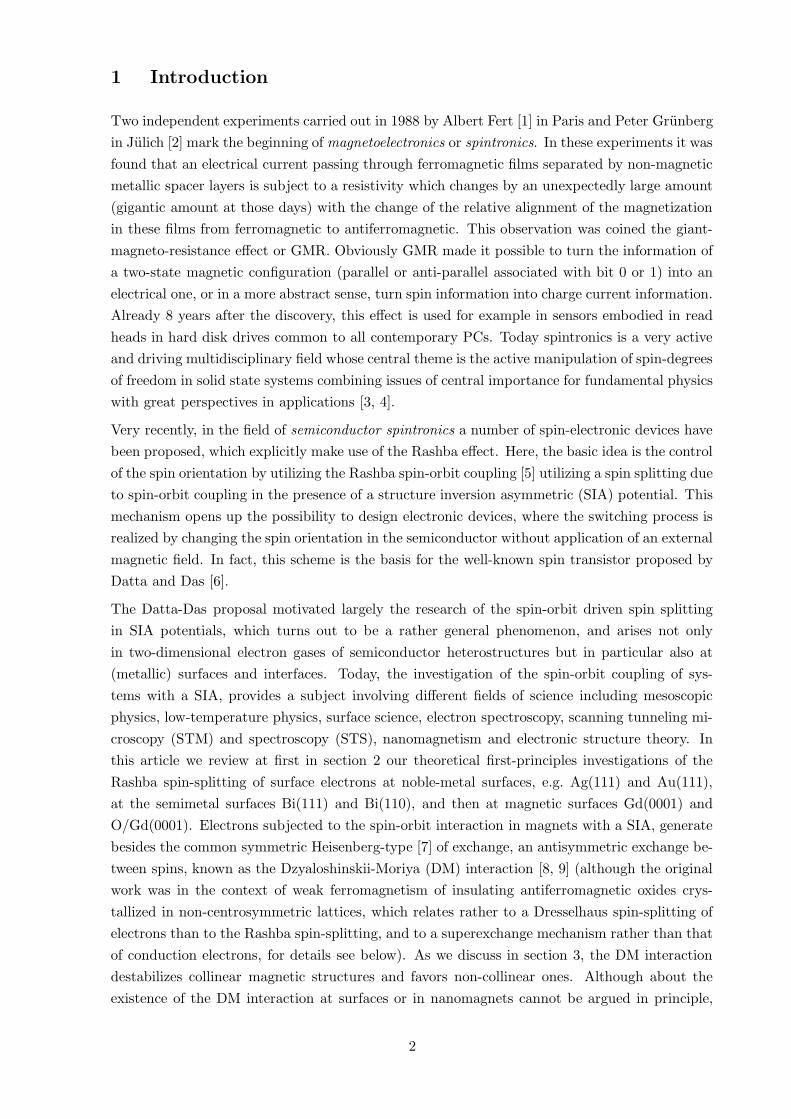
where ± denotes the spin-up and -down states with respect to a spin orientation axis n(k‖),
local in k‖ space. With the exception of the high-symmetry state k‖ = 0, we find that the
original two-fold degenerate energy paraboloid of the 2DEG in a constant potential indeed spin-
splits. The spin splitting ε+(k‖) − ε−(k‖) = 2αrk‖ is linear in k‖. Due to the presence of the
SIA potential and the spin-orbit interaction, the origin of the degenerate parabola is shifted by
kSO = m∗αR/~2, but in opposite directions for up- and down-spins with in overall spin-orbit
lowering of ∆SO = m∗αR/(2~2). The orientation axis is given by the expectation value
n±(k‖) = 〈ψ±k‖|σ|ψ±k‖
|〉 = ±
sinϕ
− cosϕ
0
⊥ k‖ = k‖
cosϕ
sinϕ
0
. (5)
We find that the orientation axis is independent of the magnitude k‖ and depends only on the
direction of the k‖ vector. In fact, it is in the plane of the 2DEG and the orientation axis is
perpendicular to the propagation direction of the electron. Considering k‖ → −k‖, ϕ changes
to ϕ + π, we find that the spin orientation axis reverses. n±(k‖) → n∓(−k‖) → −n±(−k‖).
Thus for k‖ and −k‖ the spin-up and -down states refer to opposite orientations. Defining a
global quantization axis along the line (−k‖,k‖), e.g. according to n±(+k‖), then a spin-up state
appears as spin-down state if k‖ changes sign. Together with the eigenvalue spectrum given in
equation (4) the Kramer degeneracy ε↑(k‖) = ε↓(−k‖) holds. In all, the magnetic moment is zero
when averaged over all states k‖. This is consistent with the absence of an B field. The Rashba
spin-orbit splitting may be observed either by electron photoemission or transport experiments.
In both cases experiments have to be carried out at temperatures, kBT which are lower than
the energy difference of the spin-splitting, ε+(k‖) − ε−(k‖). In angle resolved photoemission
the eigenvalue spectrum is measured for a selected k‖ value. Two peaks at different energies
are expected. Using spin-polarization analysis, for example using a Mott-detector oriented
perpendicular to the propagation direction of the electron, different polarizations should be
observed for the two peaks. Transport experiments work typically on a shell of constant energy
ε. Here we expect at a given energy two different wave vectors for up- and down-electrons, which
will be exploited in the Datta-Das proposal of a spin-transistor.
That the Pauli-like spin-orbit coupling may have important consequences for the one-electron
energy levels in bulk semiconductors was first emphasized by Dresselhaus et al. [19] already in
1955. Unlike the diamond structure of Si and Ge, the zinc blende structure, in which for example
the III-V semiconductor crystallize, exhibit a bulk inversion asymmetry (BIA), i.e. this crystal
structure lacks a center of inversion, so that we can have a spin splitting of the electron and hole
states at nonzero wave vectors k as for the Rashba effect even if B = 0. Today, this is called
the Dresselhaus effect. The corresponding Dresselhaus Hamiltonian
HD =αD
~[σxpx (p2
y − p2z) + σypy (p2
z − p2x) + σzpz (p2
x − p2y)] (6)
describes the BIA spin splitting due to the Dresselhaus spin-orbit coupling, which produces spin
vector fields quite different from those produced by the SIA splitting. One difference is obviously
that the Dresselhaus term produced a spin splitting which is proportional to k3, εD ∝ k3, while
the spin splitting of the Rashba-term is linear in k, εR ∝ k. Since we focus in this article on
spin-orbit driven physics of SIA potentials this term is not further considered.
6

1.2 Datta-Das Spin Field Effect Transistor
Figure 3 explains the Datta-Das [6] proposal of a spin field-effect transistor (SFET) exploiting
the Rashba effect. What is remarkable about this theoretical transistor model is the fact that
the tuning of the precessing spin-orientation is accomplished by applying an electric rather than
a magnetic field. Considering the fact that in semiconductor devices it is much easier to generate
electric fields as to integrate externally controllable magnetic fields, this paves a way to even
more complex devices.
Figure 3: Scheme of the Datta-Das spin field-effect transistor (SFET). The source (spin injector)
and the drain (spin detector) are ferromagnetic metals or semiconductors, with parallel alignment
of magnetic moments. The injected spinpolarized electrons with wave vector k move ballistically
through the 2DEG (which is actually quantized along a quasi-one-dimensional channel) formed
by, for example, a strained InGaAs/InP heterojunction. While propagating from source to
drain, electron spins precess about a precession axis, which arises from spin-orbit interaction,
which is defined by the structure and the materials properties of the channel. The change of the
precession angle with propagation distance is tunable by the gate voltage. The current is large if
the electron spin at the drain points in the initial direction, and small if the direction is reversed.
Shown is an intermediate situation. For simplicity we call the left ferromagnet the source, which
acts as spin injector and the right ferromagnet the drain, which acts as spin analyzer.
To understand the principle of the Datta-Das transistor we consider again a 2DEG in the
semiconductor part of the transistor located in the x-y-plane, while the quantum-well potential,
as well as the variable gate voltage, are orientated along the z-axis. We develop a simple
one-dimensional model. The x-axis is the direction of propagation for the electrons and at
the same time the polarization axis of the ferromagnetic source and drain. As we have seen
in subsection 1.1, the direction of propagation defined by k‖ determines the spin orientation
n of the eigenstates in the 2DEG, which is in the plane of the 2DEG pointing perpendicular
to the propagation direction, which is the y and −y direction in our frame of reference, i.e.
k‖ = (kx, 0, 0), ϕ = 0 and n = ±(0, 1, 0), taken the definitions entering equation (5). Neglecting
the spatial plane wave prefactor, according to equation (3) the eigenstates with respect to this
quantization axis take the form | ↑〉 = 1√2(i, 1) and | ↓〉 = 1√
2(i,−1). An electron at the point of
injection into the 2DEG next to the ferromagnetic injector is not in an eigenstate, because both
spin and propagation vector point in the same direction. But its spinor quantized along the x
7
direction, | →〉 = 1√2(1, 1) can be expressed in terms of above eigenstate as
| →〉 =1√2
(1
1
)=
1
2
[(1− i) 1√
2
(i
1
)+ (−1− i) 1√
2
(i
−1
)]. (7)
Taking into consideration that the eigenstates propagate as plane waves along the x-axis, the
x-dependent amplitude ψ(x) of the injected electron of fixed energy ε
ψ(x) =1
2
[(1− i)eik↑x| ↑〉+ (−1− i)eik↓x| ↓〉
](8)
is a coherent superposition of up- and down-states. The values k↑, k↓ belong to the opposing
spin states at fixed energy ε and can be obtained from equation (4)
k↑,↓ = κ∓ kSO with κ =
√2m∗
~ε+ k2
SO . (9)
Substituted back into equation (8), this gives the wave function the final form
ψ(x) = (cos(kSOx)| →〉 − sin(kSOx)| ←〉) . (10)
The expression includes the spinor eigenstates in x and −x direction. Here we can see for which
particular channel length L between the injector and analyzer, the spin is parallel (kSO = nπ/L)
or antiparallel (kSO = (n+1/2)π/L) to the magnetization direction of the ferromagnetic analyzer.
By calculating the spin orientation axis
n = 〈ψ(x)|σ|ψ(x)〉 =
cos(2kSOx)
0
− sin(2kSOx)
(11)
we see that the spins precess in the x-z plane. The wavelength of precession λ = π/kSO =
π~2/(m∗αR(Ez)) depends on the electric field Ez and it should in principle be possible to tune
Ez such that either full- or half-integer spin revolutions fit into the gate length L. The spin-
precession has also a classical analogon: a electron with a magnetic spin moment mx pointing
into the x-direction is injected into the 2DEG and is subject to an Rashba By-field in the y
direction. Thus, a torque τ = m×B is exerted on the magnetic moment which gives rise to a
precession of the moment in the x-z plane.
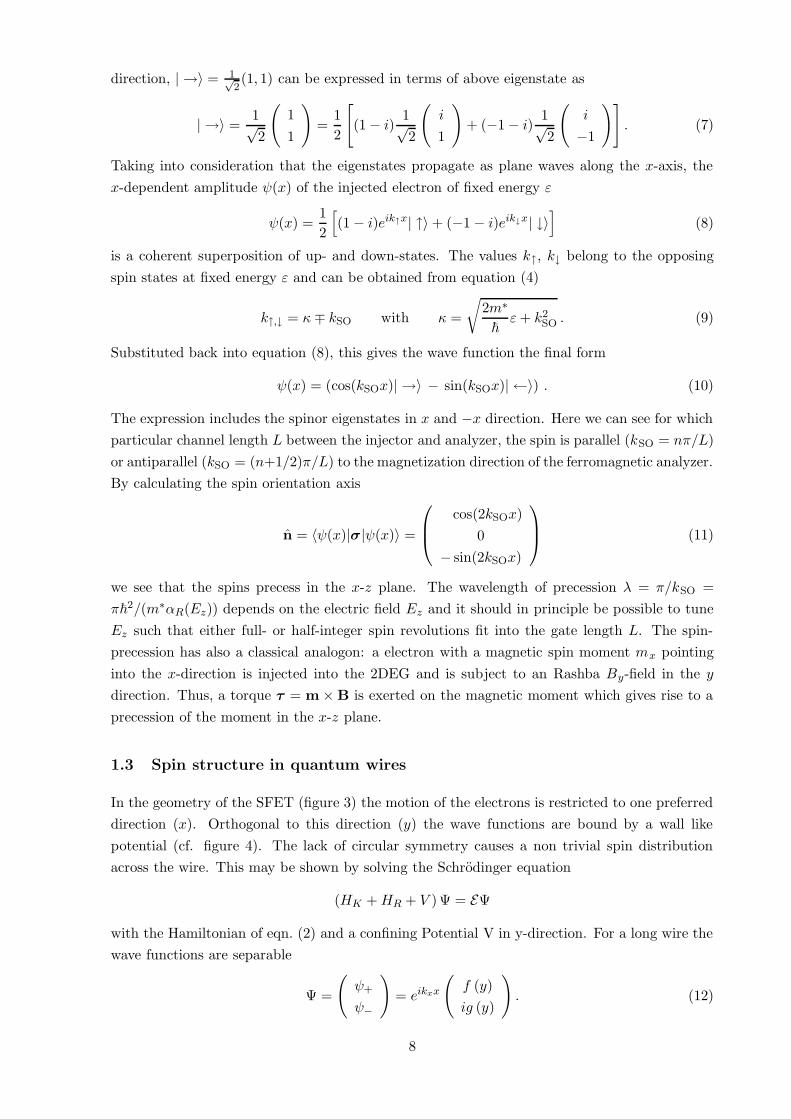
1.3 Spin structure in quantum wires
In the geometry of the SFET (figure 3) the motion of the electrons is restricted to one preferred
direction (x). Orthogonal to this direction (y) the wave functions are bound by a wall like
potential (cf. figure 4). The lack of circular symmetry causes a non trivial spin distribution
across the wire. This may be shown by solving the Schrodinger equation
(HK +HR + V ) Ψ = EΨ
with the Hamiltonian of eqn. (2) and a confining Potential V in y-direction. For a long wire the
wave functions are separable
Ψ =
(ψ+
ψ−
)= eikxx
(f (y)
ig (y)
). (12)
8

W = 600 [ nm ]L = 30 [ µ m ]
y / W
V
−.5 0 .5
εF
Figure 4: Schematic picture of a quantum wire made out of the heterostructure material of
figure 1. The typical width W and length L and position of the Fermi energy εF are indicated.
With the scaled quantities y = Ws, κ = Wkx, η = αRm∗W/~2, ε = m∗(W/~)2E , v =
m∗(W/~)2V , this results in two coupled differential equations for the spinor functions f and g:
[−1
2
(d
ds
)2
+1
2κ2 + v − ε
](f
g
)=
[0 η
(κ− d
ds
)
η(κ + d
ds
)0
](f
g
). (13)
They may be solved by standard discretization methods [20]. A typical wave function is shown
in the right of figure 5. In a wire a fraction of the kinetic energy rests in the confinement. One
− 0.5 0 0.5 y / W
V [meV ]
50
100
εF
|Ψ|2
ey
|Ψ|2
ez
Figure 5: Left: Spinor wave functions (f red, g purple) and density (blue) at εF across the wire
of figure 4. Right: Polar plot of the spin direction across the wire of the wave function shown
in the left part.
observes wave functions with increasing number of nodes across the wire at higher energies. The
local spin direction is defined by
(ex, ey, ez) =
(0 ,
2fg
f2 + g2,f2 − g2
f2 + g2
)(14)
9
and may be plotted weighted by the density in a polar diagram (right of figure 5). From left
to right, the spin direction is turned from the lower to the upper side of the wire plane. This
left right asymmetry is present in most of the stationary states and there have been attempts
to observe it experimentally [21].
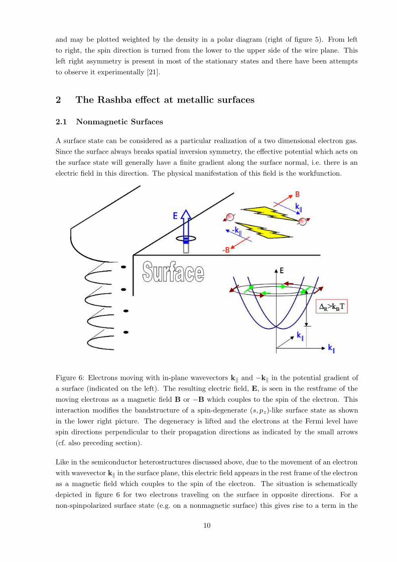
2 The Rashba effect at metallic surfaces
2.1 Nonmagnetic Surfaces
A surface state can be considered as a particular realization of a two dimensional electron gas.
Since the surface always breaks spatial inversion symmetry, the effective potential which acts on
the surface state will generally have a finite gradient along the surface normal, i.e. there is an
electric field in this direction. The physical manifestation of this field is the workfunction.
Figure 6: Electrons moving with in-plane wavevectors k‖ and −k‖ in the potential gradient of
a surface (indicated on the left). The resulting electric field, E, is seen in the restframe of the
moving electrons as a magnetic field B or −B which couples to the spin of the electron. This
interaction modifies the bandstructure of a spin-degenerate (s, pz)-like surface state as shown
in the lower right picture. The degeneracy is lifted and the electrons at the Fermi level have
spin directions perpendicular to their propagation directions as indicated by the small arrows
(cf. also preceding section).
Like in the semiconductor heterostructures discussed above, due to the movement of an electron
with wavevector k‖ in the surface plane, this electric field appears in the rest frame of the electron
as a magnetic field which couples to the spin of the electron. The situation is schematically
depicted in figure 6 for two electrons traveling on the surface in opposite directions. For a
non-spinpolarized surface state (e.g. on a nonmagnetic surface) this gives rise to a term in the
10
Hamiltonian
Hsoc =~
4m2ec
2σ · (∇V (r)× p) (15)
which leads to a k-dependent splitting of the dispersion curves. When we simply use the nearly
free electron gas (NFEG) model and substitute p by the k-vector, for usual workfunctions we
would expect this splitting to be very small, in the order of 10−6 eV. This would be far too
small to observe directly with angle resolved photoemission spectroscopy (ARPES). So it came
rather as a surprise, when in 1996 LaShell and coworkers [22] discovered a splitting of the surface
state of the Au(111) surface, which was not only k-dependent, but also in the order of 0.1 eV at
the Fermi level. They correctly interpreted this splitting as a spin-orbit coupling effect, which
obviously was influenced by the strong atomic spin-orbit effects in the heavy Au atom. Spin
resolved ARPES experiments finally also analysed the spin distribution of this surface state [23]
and found it to be in quite good agreement with the NFEG model (cf. figure 6), as it was also
predicted theoretically [24].
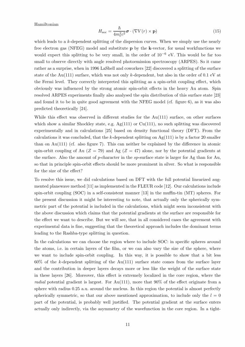
While this effect was observed in different studies for the Au(111) surface, on other surfaces
which show a similar Shockley state, e.g. Ag(111) or Cu(111), no such splitting was discovered
experimentally and in calculations [25] based on density functional theory (DFT). From the
calculations it was concluded, that the k-dependent splitting on Ag(111) is by a factor 20 smaller
than on Au(111) (cf. also figure 7). This can neither be explained by the difference in atomic
spin-orbit coupling of Au (Z = 79) and Ag (Z = 47) alone, nor by the potential gradients at
the surface. Also the amount of p-character in the sp-surface state is larger for Ag than for Au,
so that in principle spin-orbit effects should be more prominent in silver. So what is responsible
for the size of the effect?
To resolve this issue, we did calculations based on DFT with the full potential linearized aug-
mented planewave method [11] as implemented in the FLEUR code [12]. Our calculations include
spin-orbit coupling (SOC) in a self-consistent manner [13] in the muffin-tin (MT) spheres. For
the present discussion it might be interesting to note, that actually only the spherically sym-
metric part of the potential is included in the calculations, which might seem inconsistent with
the above discussion which claims that the potential gradients at the surface are responsible for
the effect we want to describe. But we will see, that in all considered cases the agreement with
experimental data is fine, suggesting that the theoretical approach includes the dominant terms
leading to the Rashba-type splitting in question.
In the calculations we can choose the region where to include SOC: in specific spheres around
the atoms, i.e. in certain layers of the film, or we can also vary the size of the sphere, where
we want to include spin-orbit coupling. In this way, it is possible to show that a bit less
60% of the k-dependent splitting of the Au(111) surface state comes from the surface layer
and the contribution in deeper layers decays more or less like the weight of the surface state
in these layers [26]. Moreover, this effect is extremely localized in the core region, where the
radial potential gradient is largest. For Au(111), more that 90% of the effect originate from a
sphere with radius 0.25 a.u. around the nucleus. In this region the potential is almost perfectly
spherically symmetric, so that our above mentioned approximation, to include only the l = 0
part of the potential, is probably well justified. The potential gradient at the surface enters
actually only indirectly, via the asymmetry of the wavefunction in the core region. In a tight-
11
binding model, Petersen and Hedegard showed that the size of the Rashba-type splitting is
determined by the product of the atomic spin-orbit coupling parameter and a measure for the
asymmetry of the wavefunction under consideration [27].
A measure for the asymmetry of the wavefunction of a surface state can be found by analysing
the l-like character of the state, i.e. to determine how much s, p or d character a surface state
shows at a certain k‖-point, in our case the Γ-point. E.g. a surface state of pure pz character is
inversion symmetric and will – in absence of an electric field – show no Rashba-type splitting.
The potential gradient or electric field at the surface will distort the wavefunction, so that some
s or dz2 contributions to the surface state will arise. The ratio of l- to l ± 1-type character of a
surface state (for a given m, e.g. m = 0) will therefore give a measure for the asymmetry of this
state. In the case of Ag(111), we find that the surface state is predominantly of pz-type, with
a small dz2 admixture (p : d ratio of 9.5) while in Au the surface state has much stronger dz2
character (p : d = 3.3). The fact that the Au d band lies much higher in energy than the Ag d
band leads to a stronger d character of the Au surface state and thus to larger asymmetry of the
wavefunction [26]. This determines the stronger k-dependent splitting in the Au(111) surface
bandstructure.
-0.2 -0.1 0 0.1 0.2
k|| along ΓM (Å
-1)
-0.6
-0.4
-0.2
0.0
0.2
0.4
E -
EF (
eV)
Au(111) pz:d
z2 = 13:4
1 ML Ag on Au(111)
-0.2 -0.1 0 0.1 0.2
Ag (111) pz:d
z2 = 39:4
1 ML Au on Ag(111)
Figure 7: Bandstructure of Au(111) (left, full circles) and one monolayer Ag on Au(111) (left,
open circles) as compared to a Ag(111) film (right, full symbols) and a single Au monolayer on
Ag(111) (right, open symbols).
This effect can be further demonstrated, when we compare a single monolayer of Ag on Au(111)
12
with a Au monolayer on Ag(111). Just from the point of view of the atomic SOC, we would
expect that the Rashba-type splitting of the Au monolayer of Ag(111) is larger than that of
the Ag/Au(111) system, since more than 50% of the effect comes from the surface layer. But
since the gold d states of the subsurface layers can induce a larger d character of the Ag surface
state in Ag/Au(111) while the Au surface state of Au/Ag(111) has less d character than the
one of pure Au(111), finally the Rashba-type spin-orbit splitting is larger in Ag/Au(111) (cf.
figure 7). Other examples, how the asymmetry of a surface state influences the strength of the
Rashba-type splitting can be found on lanthanide surfaces (e.g. Lu(0001) [26]), and a particular
case will be presented in subsection 2.3.
2.2 Semimetal Surfaces
Up to now we have discussed examples, where the Rashba-type spin-orbit splitting was in the
order of 10 to 100 meV (up to 120 meV for Au(111)), so that experimentally it is not so easy to
detect in ARPES experiments. Now, we turn to another extreme, where the splitting is so big,
that it was not a-priori clear, whether the two experimentally observed features were spin-split
partners of the same state or two different surface states: the low-index surfaces of Bi. Bismuth
is a non-magnetic, rather heavy metal (Z = 83) with semimetallic properties, i.e. the Fermi
surface consists only of two tiny pockets, so that the density of states (DOS) at the Fermi level
(EF) is almost zero. In the surface projected bulk-bandstructure extended gaps are observed
around EF, in which surface states can be localized.
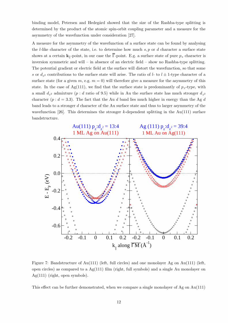
ARPES measurements on the Bi(110) surface [28] showed the existence of two spectroscopic
features in the gap, which could be interpreted as to two surface states. Bismuth has a rhom-
bohedral crystal structure and the (110) surface consists of unreconstructed pseudocubic bilay-
ers [29], where dangling bonds can give rise to surface states. Similarly, on Bi(111) two states
were identified spectroscopically [30]. The (111) surface has closed-packed layers and again
shows a bilayer structure, but without dangling bonds and with a much larger separation of
the bilayers [31]. In both cases of course only the occupied part of the surface bandstructure
could be observed spectroscopically. Using DFT calculations, we have the possibility to access
also the unoccupied part of the spectrum. It can be seen that the observed spectroscopic fea-
tures are actually a Rashba-type spin-split pair of a surface state which forms – at least for the
(110) and (100) surface – a band through the whole surface Brillouin zone [32, 33]. That these
surface state is actually split by spin-orbit coupling can be demonstrated by comparison of a
scalar-relativistic calculation without inclusion of SOC and with the inclusion of SOC [34] (cf.
also left of figure 8). In this cases, the splittings are very large (in the order of 300 meV) and,
since the surface states extend throughout the Brillouin zone, they are also no longer linear in
k, except in the vicinity of high symmetry points.
It is not only of academic interest, whether two surface states are a spin-split pair or two spin-
degenerate surface states. For example, on the Bi(111) surface the Fermi surface forms a small
hexagon around the Γ point, which led to speculations about the formation of a charge density
wave on this surface [35]. If the Fermi surface were indeed formed by spin-degenerate surface
states, this would be possible. If, on the other hand, Rashba-type spin-split bands form this part
of the Fermi surface, the electrons at +k‖ and −k‖ were of opposite spin and instead of a peak
13

in the (spin) diagonal part of the susceptibility χ, we would expect a large contribution to the
spin off-diagonal part, χ±, leading to a modulation of the spin-structure. Since the surface is of
course still nonmagnetic, these modulations have to cancel and a direct observation is difficult.
When magnetic atoms were present at the surface, their interaction would be modified and this
effect could be detected. We will show in a later chapter, that this is actually possible.
Using scanning tunneling microscopy (STM) techniques, consequences of the spin polarization of
the surface states have indeed been observed for another Bi surface [32]. If a scanning tunneling
spectrum (STS) is recorded for a dense mesh of positions on a surface, this STS map can be
Fourier transformed for a given energy within this spectrum. The Fourier transformed (FT) STS
map gives then a picture of the energy dispersion in reciprocal space, i.e. a two dimensional cut
through the function ε(k‖), but with doubled length of the k-vectors, since the STS maps the
scattering between two states of different k but at the same E. In particular, for E = EF, this
yields an image the Fermi surface. It is easily seen, that a surface state with a Fermi surface of
a wavevector ±kF will give rise to standing waves with 2kF which can be seen in the STS map.
This correspondence between FT-STS and Fermi surface has been used extensively to study the
electronic properties of high-temperature superconductors. A Rashba splitting will not change
this picture, since for one spin channel the Fermi vectors are changed to ±kF + ∆k, while for
the other spin we get ±kF−∆k, so that both spin channels will lead to a contribution of ±2kF
in the STS map, i.e. the picture is indistinguishable from the one without Rashba splitting [27].
But if the Fermi surface is more complex, like in the case of Bi(110), the fact, that the surface
states are spin polarized can be seen the FT-STS clearly.
K Γ M
-0.4
-0.2
0.0
0.2
0.4
E -
EF (
eV) proj. bulk bands
surf. state w.o. SOCsurf. state with SOC
K Γ M
projected bulk bands10 BL film statessurface states
Figure 8: Bulk-projected bandstructure of Bi and surface bandstructure of a 22 layer Bi(111)
film with H termination on one side (left) with (full line) and without (broken line) spin-orbit
coupling included in the calculation. A similar calculation with SOC included for a symmetric
20 layer film without H termination is shown on the right.
Consider a simple one-dimensional example: along the line ΓM in Bi(111) we can see in figure 8
(left, broken line) a surface state obtained without inclusion of SOC. This state originates at
14

−0.3 eV at Γ, crosses the Fermi level at a wavevector we denote ka, disperses down again and
crosses EF once more at kb and reaches M at −0.22 eV. Surface states at EF can scatter between
ka and kb and give rise to standing waves with wavelength 2ka, 2kb, (ka + kb) and (ka − kb), if
the state is spin-degenerate. Now, consider that spin-orbit coupling splits this degeneracy and
gives rise to spin-up states at ka + ∆k and kb−∆k, while spin-down states cross the Fermi level
at ka −∆k and kb + ∆k. In this case, spin conserving scattering events will again give rise to
oscillations with wavelength 2ka, 2kb, but also (ka + kb) ± 2∆k and (ka − kb)± 2∆k. Here, the
effect of spin is clearly visible. On the Bi(110) surface, this effect was also verified experimentally
in a two dimensional case [32].
The occurrence of spin-polarized surface states of course suggests, that this could be utilized in
some way for spintronic applications. In the case of Ag(111), where the surface state contributes
very little to the density of states at the Fermi level, this might not seem very promising, but in
the case of a semimetal surface, where the DOS at EF originates almost exclusively from surface
states, this might be more realistic. Alternatively, the surface of a thin film on insulating or
semiconducting substrates could be interesting, since in this case the relative contribution of the
surface state to the conduction electrons is also increased. This works of course only, if the thin
film still supports the same surface state as the semiinfinite crystal, i.e. localized Tamm states
of d-character as they occur on lanthanide (0001) surfaces will be more suitable for very thin
films than the extended s, p-derived Shockley states of the closed packed coinage metal surfaces.
Another effect, that can disturb the surface states in thin films, is the interaction between the
two surfaces of the film. If, like in Bi, the screening is very weak, surface states at the upper
and lower surface of a symmetric film interact to form even and odd linear combinations. This
of course interferes with the concept of broken inversion symmetry at the surface. On the other
hand, in our theoretical calculations for Au and Ag surfaces, we always used symmetrical films
where a tiny interaction between upper and lower surface cannot be avoided, even in thicker
films. For the bandstructures of figure 7 we used 23 layer films and especially in the case of
Ag(111), a finite splitting of the surface state parabolas at the Γ point can be seen. At the
first glance it might seem surprising, that the two different splittings, the even-odd and the
Rashba-type splitting result in only two dispersion curves. Without the interactions that lead
to the splittings, we can think of having two states (spin up, ↑ and down, ↓) on each surface.
The spin-orbit coupling leads for the spin up states of the upper surface (↑u) to the same shift
in energy as for the spin down states of the lower surface (↓l) (since the potential gradient is
reversed there) and they will have an energy ε+. In the same way of course ε(↓u) = ε(↑d) = ε−.
A hybridization of ↑u and ↓u leads to energies ε+ + εs and ε−− εs, respectively, but in the same
way the two downspin states, ↓u and ↓l will be shifted to energy values ε− − εs and ε+ + εs.
The stronger the interaction across the film, the more each state will be localized at both sides
of the film so that finally the spin-polarization for a given energy and k‖ gets reduced.
A case, where this scenario has been actually observed in experiment are thin Bi films grown
on a Si substrate [36]. The interaction with the substrate is very weak, since the Bi film is
deposited on a seeding layer of Bi atoms and can adopt (for more than a few bilayers) the
structure of Bi(111). Angle resolved photoemission has shown that near the zone center the
electronic structure of these Bi films is not so different from what has been observed on single
crystal surfaces. But when the k‖ vector approaches the zone boundary at M, the crossing of the
15
two spin-split states is no longer observed. Instead, quantum well states (QWS) are formed when
the surface state gets near to the bulk continuum at M [36]. The energy levels of these states
agree nicely with those obtained by the calculation of symmetric films of the same thickness
(cf. right of figure 8). As the surface state character is lost, also the spin-polarization of these
states vanishes. The very bad screening of Bi makes this QWS disappear only for very thick
films (more than 40 bilayers). Therefore, when we simulate Bi single crystal surfaces, we have
to terminate one side of the film with H atoms to saturate the dangling bonds and explicitly
remove the inversion symmetry of the film, even if it is 22 layers thick.
2.3 Magnetic Surfaces
Let us finally consider the case of a surface of a magnetic metal, like Gd(0001). On this closed
packed surface a bulk projected bandgap around Γ contains a surface state of dz2 character, like
it can be found also on other lanthanide surfaces. Exchange interaction splits this surface state
into an occupied majority spin state and an unoccupied minority state. This splitting is mainly
controlled by the 4f electrons of Gd and amounts to about 0.8 eV, which is large as compared to
spin-orbit effects in this system. No matter how SOC affects the electrons of the surface state,
their spin will remain more or less parallel to the exchange field, which is oriented in plane in
the directions of nearest neighbor atoms by the magnetic anisotropy.
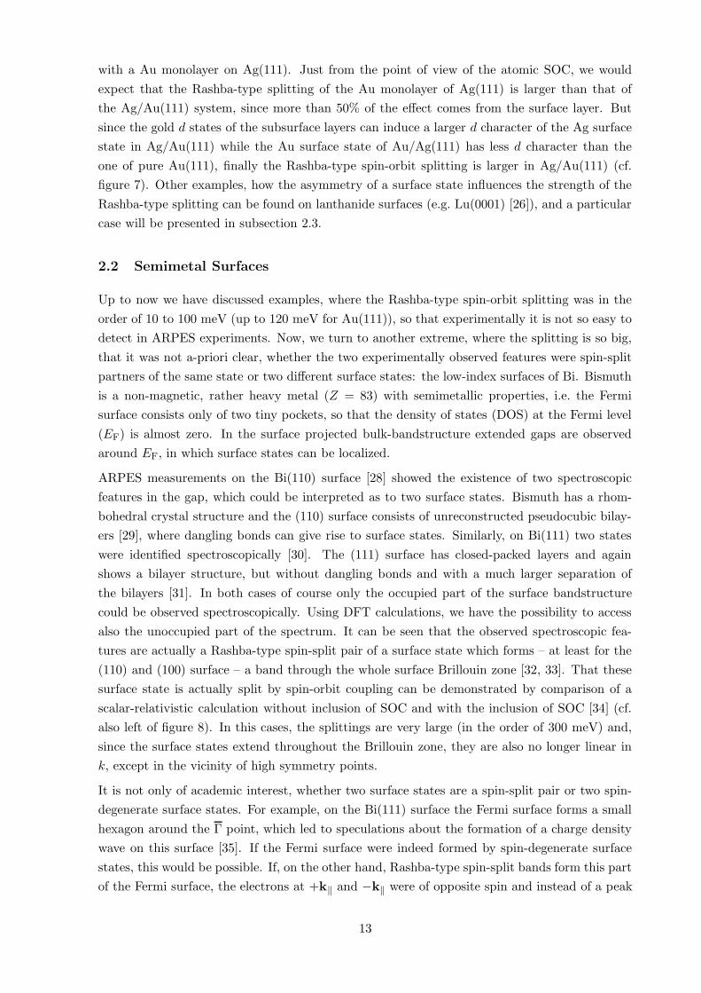
An electron traveling on the surface in a direction perpendicular to its spin quantization axis,
will experience the potential gradient at the surface as a magnetic field parallel to its spin.
Therefore, a magnetic coupling can arise and the dispersion curves will split more or less similar
to what is observed on a nonmagnetic surface. If, on the other hand, the propagation direction
of the electron is parallel to its spin quantization axis, the field arising from SOC cannot couple
to the electron’s spin and no Rashba-like splitting can be observed. Schematically, this situation
is shown in figure 9. In contrast to the surface state on the nonmagnetic surface, where the spin
of the electron is always oriented perpendicular to the propagation direction and the surface
normal, ez, (with some deviation, depending on the shape of the potential [24]), on the spin-
polarized surface, the spins are more or less collinear. This changes the shape of the Fermi
surface significantly, especially if exchange splitting is considered (figure 9 (c)). If the exchange
splitting is large, this leads to a Fermi surface consisting of a single circle shifted away from the
zone center. The consequences for the bandstructure are simple: along a certain direction in
reciprocal space SOC will have no particular effect. In a direction orthogonal to this one, the
dispersion curves for majority and minority spin will be shifted in opposite directions. For the
eigenvalues this results in an expression
ε↓(↑)(k) = ε(k)± IM ± αR(k× ez) · M (16)
where M = MM is the magnetization and IM represents the exchange splitting of the bands.
Of course in a calculation of a symmetric film, again on the lower surface (−ez) the directions
of the spin-orbit induced shifts will be exactly opposite to the shifts on the upper surface,
so that in total a picture as shown in figure 9 (d) is obtained. From this picture the two
splittings for the spin-up and the spin-down surface state can be determined directly as ∆ε(k) =
ε(k,M) − ε(k,−M).
16
ky
kx
kyky
E
E
E
EEky
E E
kx
(b) (c) (d)(a)
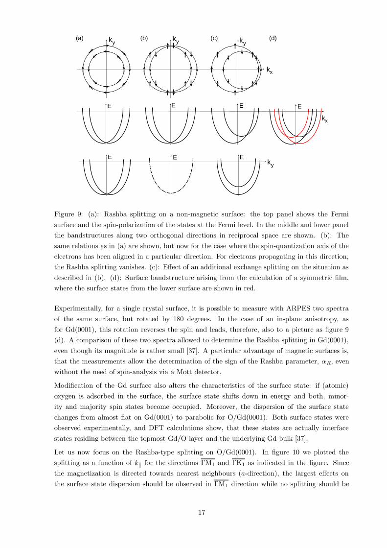
Figure 9: (a): Rashba splitting on a non-magnetic surface: the top panel shows the Fermi
surface and the spin-polarization of the states at the Fermi level. In the middle and lower panel
the bandstructures along two orthogonal directions in reciprocal space are shown. (b): The
same relations as in (a) are shown, but now for the case where the spin-quantization axis of the
electrons has been aligned in a particular direction. For electrons propagating in this direction,
the Rashba splitting vanishes. (c): Effect of an additional exchange splitting on the situation as
described in (b). (d): Surface bandstructure arising from the calculation of a symmetric film,
where the surface states from the lower surface are shown in red.
Experimentally, for a single crystal surface, it is possible to measure with ARPES two spectra
of the same surface, but rotated by 180 degrees. In the case of an in-plane anisotropy, as
for Gd(0001), this rotation reverses the spin and leads, therefore, also to a picture as figure 9
(d). A comparison of these two spectra allowed to determine the Rashba splitting in Gd(0001),
even though its magnitude is rather small [37]. A particular advantage of magnetic surfaces is,
that the measurements allow the determination of the sign of the Rashba parameter, αR, even
without the need of spin-analysis via a Mott detector.
Modification of the Gd surface also alters the characteristics of the surface state: if (atomic)
oxygen is adsorbed in the surface, the surface state shifts down in energy and both, minor-
ity and majority spin states become occupied. Moreover, the dispersion of the surface state
changes from almost flat on Gd(0001) to parabolic for O/Gd(0001). Both surface states were
observed experimentally, and DFT calculations show, that these states are actually interface
states residing between the topmost Gd/O layer and the underlying Gd bulk [37].
Let us now focus on the Rashba-type splitting on O/Gd(0001). In figure 10 we plotted the
splitting as a function of k‖ for the directions ΓM1 and ΓK1 as indicated in the figure. Since
the magnetization is directed towards nearest neighbours (a-direction), the largest effects on
the surface state dispersion should be observed in ΓM1 direction while no splitting should be
17

0.3 0.2 0.1 0 0.1 0.2 0.3k|| (Å
-1)
-100
-50
0
50
100
∆ ε
(m
eV
)
M1
← Γ → K1
O/Gd S↑
O/Gd S↓
Gd S↑
M1
M2
K2
K1
Γ
Figure 10: Left: Magnetization direction on the Gd(0001) surface indicated by the red arrow and
surface Brillouin zone and labeling of the high symmetry points. Right: Rashba-type splitting
of the surface state of Gd(0001) and O/Gd(0001) in the directions ΓK1 and ΓM1.
visible in the direction ΓK2. A closer look at figure 10 reveals, that the splitting, ∆ε is indeed
smaller in ΓK1 than in ΓM1. Furthermore, we observe that ∆ε for the majority spin state
(S↑) is not only of opposite sign as compared to ∆ε for the minority state (S↓), but also their
absolute values differ. This is also observed experimentally, and can be explained again by the
different positions of the states in the bulk-projected bandgap and the different asymmetry of
the wavefunctions. One should note here, that also the effective masses of the S↑ and S↓ states
differ and this shows, that spin is not the only difference of these states.
Even more drastic is the difference of the S↑ surface state of O/Gd(0001) to the S↑ state of
Gd(0001). We can see from the right of figure 10 that not only the magnitude of the splitting is
a factor 3 to 4 smaller, even the sign is different. Since this reversal of sign cannot be attributed
to the spin, it must result from a different admixture of pz-character to the dz2 surface state. A
reversal of the gradient of the wavefunction at the position of the Gd nucleus can be interpreted
as the result of hybridization with pz-type wavefunctions of different signs. In some sense we
can say, that we see the sign of the wavefunction here in the sign of the Rashba-parameter.
3 Anisotropic exchange of adatoms on surfaces
In the last subsection, we assumed that the magnetic order at the surface is not influenced by
spin-orbit coupling effects. If the exchange field is strong, all spins will align accordingly. On
the other hand, if the exchange coupling is weak, spin-orbit coupling effects can substantially
influence the magnetic interaction. The particular case of two distant impurities, which interact
in a RKKY-type manner via a non-magnetic host which shows strong spin-orbit effects has
been discussed by Smith [38]. He showed that the interaction between two magnetic atoms A
and B (spins SA and SB) via a non-magnetic third atom with a SOC term l · s gives rise to
an interaction (SA · s)(l · s)(s · SB). Taking the trace over the spin variable s this term can
be written as (−i/4)l · (SA × SB) and thus shows the form of the Dzyaloshinskii-Moriya (DM)
18

interaction D · (SA×SB). Fert and Levy [39] derived an expression for this anisotropic exchange
interaction of two magnetic atoms in spin-glasses doped with heavy impurity atoms which is of
the form
HDM = −V (ξ)sin [kF(RA +RB +RAB) + η] RA · RB
RARBRAB(RA × RB)(SA × SB) (17)
where RA = RARA and RB = RBRB are the positions of the magnetic atoms measured from
the nonmagnetic impurity and RAB is the distance between the atoms A and B. V (ξ) is a
term that depends of the spin-orbit coupling constant of the nonmagnetic atom, ξ, kF is the
Fermi vector and η the phase shift induced by the impurity. The sinus term reflects the RKKY-
type character of the interaction, while the two cross products determine the symmetry of the
interaction.
RA RB
RA RBx
SA SBSA SBx
RA RB
RA RBx
SASB
SA SBx
Figure 11: Two magnetic adatoms (A,B) on a surface interacting with a surface atom at the
center. The distance between the surface atoms and the adatoms is RA and RB . The spins of
the adatoms are almost perpendicular to the surface (left) or in the surface plane (right), but
sightly canted to give a finite value for SA × SB
This model can be translated to the case of two magnetic atoms on a surface, where the magnetic
interaction is mediated by surface states which show strong SOC effects. Such a situation might
be imagined, if e.g. two Mn atoms are placed on a Bi surface (figure 11). If the easy magnetic axis
is out-of-plane, a slight tilting of the magnetic moments results in a finite value for SA×SB which
is then parallel to RA × RB and leads to a non-vanishing contribution of HDM (equation (17)).
If the easy magnetic axis is in-plane (right of figure 11) and the surface normal is the hard axis,
a small tilting of the magnetic moments results in a vector SA×SB that is normal to RA× RB
and equation (17) will give no contribution to the total energy. Of course, on a surface the
scattering will involve all surface atoms and in general it will depend not only on the direction
of the spins of the adatoms, but also on the symmetry of the surface whether a DM interaction
will occur for a specific arrangement of the spins. This will be discussed later in more detail.
If we extend the two impurities in figure 11 to a chain of magnetic atoms, where the spins of
two neighbouring atoms, i and j, are canted slightly, an interaction of this kind
HDM = Dij · (Si × Sj) (18)
will favour spin-spiral structure. Since the DM interaction has to compete with the Heisenberg-
type (symmetric) exchange interaction, these structures will probably be of long wavelength.
Such long-ranged magnetic structures can be found on surfaces in domain walls of thin magnetic
films. In the following we will discuss the consequences of the DM interaction on this kind of
19

long ranged, non collinear structures, and show results of ab initio calculations for a system that
has also been investigated experimentally in some detail.
4 Mesoscale magnetic structures
In this section, we discuss magnetic structures on the mesoscopic length scale that are driven
by the DM interaction. Since the DM interaction is a purely relativistic effect, we expect it to
be much weaker than the usual exchange interactions. In most cases, it cannot cause more than
a small canting angle between the spins on adjacent lattice sites, and the local magnetic struc-
ture (typically ferro- or antiferromagnetic) is governed by non-relativistic effects. For spatially
slowly varying magnetic structures, however, the DM interaction can become relevant since it is
antisymmetric whereas the non-relativistic exchange interactions are all symmetric with respect
to the canting angle. The symmetric interactions lack any linear terms in the usual Taylor
expansions in the canting angle, whereas an antisymmetric interaction shows such a term. In
the following, we employ a simple model in order to describe the mesoscale magnetic structures
that can arise from an interplay of spin stiffness, usual anisotropy and the Dzyaloshinskii-Moriya
interaction. It is not the aim of this section to give a complete overview of the possible magnetic
structures arising from the DM interaction at surfaces, but our simple model already illustrates
the variety of possible magnetic structures.
4.1 Micromagnetic model
We restrict our further investigations to a quasi one-dimensional model where the magnetization
depends on only one spatial coordinate x, and we denote the corresponding real-space direction as
propagation direction (cf. figure 12). The quasi one-dimensional model is justified for anisotropic
row−1 S−1,−1&%
'$S−1,−1&%
'$S−1, 0&%
'$S−1, 0&%
'$S−1,+1&%
'$S−1,+1&%
'$S−1,+2&%
'$S−1,+2&%
'$row 0 S 0,−1&%
'$S 0,−1&%'$
S 0, 0&%'$S 0, 0&%'$
S 0,+1&%'$S 0,+1&%'$
row+1 S+1,−1&%'$S+1,−1&%'$
S+1, 0&%'$S+1, 0&%'$
S+1,+1&%'$S+1,+1&%'$
S+1,+2&%'$S+1,+2&%'$
row+2 S+2,−1&%'$S+2,−1&%'$
S+2, 0&%'$S+2, 0&%'$
S+2,+1&%'$S+2,+1&%'$
x
JJ
Figure 12: Atomic rows. In
the quasi one-dimensional model,
we assume that the magnetiza-
tion direction changes along the
x-direction but remains constant
within a row normal to the x-
direction (i.e. Sj,i = Sj,i′ ). The
x-direction is called propagation
direction.
crystal structures where the magnetization is expected to propagate along a high-symmetry line
and for simple domain walls where the magnetization is expected to propagate normal to the
real-space orientation of the domain boundary. But our ansatz cannot describe vortices and
other mesoscale magnetic structures that are well discussed in literature (cf. e.g. [40]).
As we want to investigate magnetic structures, that change on length scales that are large
compared to the lattice spacing, we can employ a micromagnetic model. In such a model, the
magnetization direction is not described by a discrete set of unit vectors Sj but by a contin-
20
uous function m(x) with |m| = 1 . This ansatz works for ferromagnetic and antiferromagnetic
materials alike: In the case of an antiferromagnetic structure, m(x) is oriented parallel and
antiparallel respectively to every second atomic moment Sj .
If all relevant interactions are reasonably short-ranged, we can estimate the energy of a magnetic
configuration (in a homogeneous crystal) by
E[m] =
∫dx f(m, m) (19)
with m(x) = dd x m(x) . The structure of the function f can be deduced from a discrete lattice
model, for instance the classical Heisenberg model∑
i,j Ji,j Si · Sj corresponds to a term of the
form∫
dxA m(x)2 (cf. e.g. [41]). But the integrand A m(x)2 can also be regarded as the lowest
order Taylor expansion to an arbitrary symmetric m-dependent function. Thus, the parameter
A includes all non-relativistic exchange effects in the limit of spatially slowly varying magnetic
structures, even if the system is badly described by the Heisenberg model.
In the following, we consider a term symmetric in m (that prevents spin rotations on short
length scales), a term antisymmetric in m (that favors certain spin rotations), and the lowest
order anisotropy term and we work with the energy functional
E[m] =
∫dx(A m(x)2 + D·( m(x) × m(x) ) + m(x)† ·K·m(x)
) ). (20)
The model parameters are the spin stiffness A, the Dzyaloshinskii vector D and the anisotropy
tensor K. As we assume, that the magnetization propagates along a high symmetry line of a
rectangular surface, we know the direction of the Dzyaloshinskii vector D and the structure of
the anisotropy tensor K: D is oriented perpendicular to the x-direction and perpendicular to
the surface normal (cf. figure 13), and K is diagonal if we choose our coordinate axis along the
high symmetry directions of the crystal. With such a coordinate system, we get:
D =
0
0
D
, K =
K1 0 0
0 K2 0
0 0 KD
. (21)
4.2 Planar spin structures
From equation (20) it is obvious, that the DM term is minimized if the magnetization rotates
in the plane normal to the Dzyaloshinskii vector D. If the hard axis is oriented parallel to D
(i.e. KD>K1 , KD>K2 ), then the anisotropy term also favors a magnetization that is confined
to the plane normal to D. At first, we restrict our considerations to this case. In such a system
with m ⊥ D, we can describe the magnetization with only one angle ϕ ( m = e1 cosϕ+e2 sinϕ )
and obtain the energy functional
E[ϕ] =
∫dx(A ϕ(x)2 +D ϕ(x) +K sin2 ϕ(x) + const
)(22)
with K = K2 −K1 . Without loss of generality, we assume K > 0 . The functional (22) is well
discussed by Dzyaloshinskii. In the following we briefly state some of his results, for further
details and analytical derivations cf. [42, 43].
21

D
−→
(a) (b) (c)
Figure 13: Spin spirals with different rotation axes on a symmetric surface. For each rotation
axis, a right- and a left-handed spiral is shown. If we neglect the substrate, the right- and left-
handed spirals are mirror images of each other. If we take spin-orbit coupling into account, we
need to consider the system consisting of spiral and substrate. For (a) and (b), the mirror plane
is oriented normal to the surface, therefore the surface does not break the mirror symmetry
(provided that the spirals propagate along a high-symmetry line of the crystal structure). In
the case (c), however, the surface breaks the mirror symmetry and there is no other symmetry
operation mapping the right- onto the left-handed system. Therefore, the two systems in (c) are
not equivalent to each other and may differ in energy. With equation (18), we conclude that D
is orthogonal to the rotation axes of (a) and (b). Of course, the sign of D cannot be deduced
from the symmetry.
If we neglect the anisotropy term K sin2 ϕ, we obtain spin rotations for all non-vanishing D.
But, for sufficiently large K the DM term cannot compete with the other terms and the energy
is minimized by a collinear magnetization that is oriented along the easy axis (i.e. ϕ(x) = 0 =
const ). The model (22) shows a rotating spin structure as the ground state, if and only if
|D| > 4
π
√AK ⇔ |D| = |D|√
AK>
4
π. (23)
At the transition to the collinear ground state, the spiral’s spatial period length λ diverges (cf.
figure 14). This transition can be interpreted as a second-order phase transition with order
parameter 1/λ and a kink in dE/dD .
If the DM term is not strong enough to cause a rotating spin structure, a ferromagnetic sample
of sufficient size usually consists of several domains that posses different spin quantization axes.
In this case, we can use equation (22) with the boundary conditions
ϕ(x)x−∞−−−−→ π , ϕ(x)
x+∞−−−−→ 0 (24)
in order to describe a wall between two oppositely magnetized domains. Thereby, the size of
the DM term cannot influence the domain-wall shape ϕ(x) but alters the wall energy E:
E =
+∞∫
−∞
dx(A ϕ2 +K sin2 ϕ
)+
+∞∫
−∞
dxD ϕ with
+∞∫
−∞
dxD ϕ =
π±π∫
π
dϕ D = D (±π) . (25)
Minimizing the (A,K)-dependent term in equation (25) yields two degenerate solutions of oppo-
site rotational directions, i.e. with opposite sign of ϕ(x). The D-dependent term is independent
22
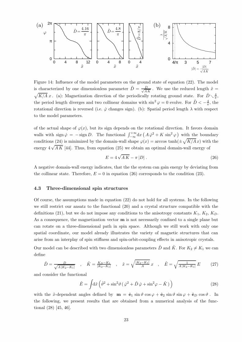
(a)
0 4 8 12 0 4 8 0 40
π
2π
ϕ
x x x
D=4.16
πD=
4.8
π
D=
8/π (b)
4/π 3 5 70
4
8
λ√
A/K
|D| =|D|√AK
Figure 14: Influence of the model parameters on the ground state of equation (22). The model
is characterized by one dimensionless parameter D = D√AK
. We use the reduced length x =√K/A x . (a): Magnetization direction of the periodically rotating ground state. For D 4
π ,
the period length diverges and two collinear domains with sin2 ϕ = 0 evolve. For D < − 4π , the
rotational direction is reversed (i.e. ϕ changes sign). (b): Spatial period length λ with respect
to the model parameters.
of the actual shape of ϕ(x), but its sign depends on the rotational direction. It favors domain
walls with sign ϕ = − signD. The functional∫ +∞−∞ dx
(A ϕ2 +K sin2 ϕ
)with the boundary
conditions (24) is minimized by the domain-wall shape ϕ(x) = arccos tanh(±√K/Ax) with the
energy 4√AK [44]. Thus, from equation (25) we obtain an optimal domain-wall energy of
E = 4√AK − π |D| . (26)
A negative domain-wall energy indicates, that the the system can gain energy by deviating from
the collinear state. Therefore, E = 0 in equation (26) corresponds to the condition (23).
4.3 Three-dimensional spin structures
Of course, the assumptions made in equation (22) do not hold for all systems. In the following
we still restrict our ansatz to the functional (20) and a crystal structure compatible with the
definitions (21), but we do not impose any conditions to the anisotropy constants K1, K2, KD.
As a consequence, the magnetization vector m is not necessarily confined to a single plane but
can rotate on a three-dimensional path in spin space. Although we still work with only one
spatial coordinate, our model already illustrates the variety of magnetic structures that can
arise from an interplay of spin stiffness and spin-orbit-coupling effects in anisotropic crystals.
Our model can be described with two dimensionless parameters D and K. For K2 6= K1 we can
define
D = D√A |K2−K1|
, K = KD−K1
|K2−K1| , x =
√|K2−K1|
A x , E =√
1A |K2−K1| E (27)
and consider the functional
E =
∫dx(ϑ2 + sin2ϑ ( ϕ2 + D ϕ + sin2ϕ− K )
)(28)
with the x-dependent angles defined by m = e1 sinϑ cosϕ + e2 sinϑ sinϕ + eD cosϑ . In
the following, we present results that are obtained from a numerical analysis of the func-
tional (28) [45, 46].
23

Figure 15: Noncollinear ground state of the functional (28). The left picture shows a planar
rotating state (ϑ = π/2) that occurs for large |D|, the right picture shows the state that occurs
for intermediate values of |D|. The latter performs a truly three-dimensional path in spin space
with ϑ 6= const . Note, that m tries to avoid the hard axis that is oriented vertically in this
figure.
1.0 4/π
0.0
0.1
b
a
K=
KD−
K1
|K2−
K1|
D =
D√
A |K2 − K1|
Col ⊥ D
Col ‖D
NC⊥
D
3-dim
Figure 16: Phase diagram of the ground state of the functional (28). The diagram shows
the collinear phase with m aligned perpendicular (Col ⊥ D) or parallel (Col ‖D) to D, the
noncollinear (rotating) phase where m is confined to a plane (NC ⊥ D) and the noncollinear
phase where m describes a truly three-dimensional path in spin spin space (3-dim). For D < 0
equivalent noncollinear phases occur with reversed rotational direction. The solid line denotes
a first-order and the dashed lines denote continuous transitions. The two dashed lines approach
each other for increasing (−K). For K1 = K2 the intermediate region (3-dim) vanishes and there
is a sharp transition from the collinear state (Col ‖D) to the planar rotating state (NC⊥D).
Due to our choice of the reduced parameters (equation (27) ), this transition point cannot be
displayed in this figure.
For small |D|, the anisotropy term dominates the DM term and the ground state is collinear
(ϑ = 0 = const), for large |D| the system is dominated by the competition between the DM
interaction and the spin stiffness and the rotating magnetization is confined to the plane normal
24
to the Dzyaloshinskii vector (ϑ = 12 π = const , left picture in figure 15). If D points parallel
to the easy axis (i.e. K < 0 ), there is a continuous transition from the collinear to the planar
rotating ground state: When |D| exceeds a certain critical value, then the magnetization starts
to rotate around the D-vector (i.e. sign ϕ = − sign D = const ), and the average cone angle ϑ
increases with increasing |D| (right picture in figure 15). If D does not point parallel to the easy
axis, there is no continuous transition from the collinear to a rotating ground state possible: In
this case a rotation around the D-vector cannot be realized by an infinitesimal deviation from
the collinear state. In figure 15 we illustrate the rotation path m(x) of the ground state, in
figure 16 we show the resulting phase diagram.
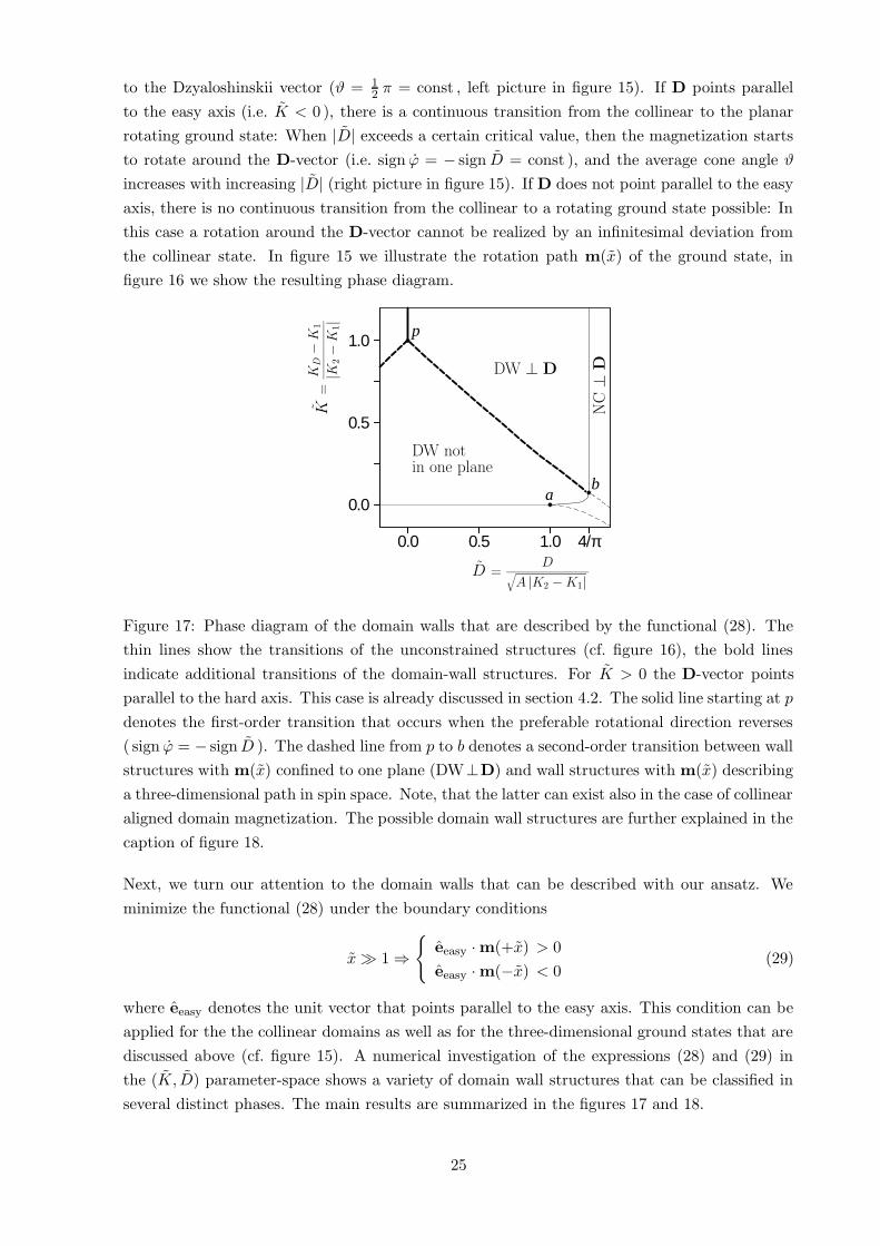
0.0 0.5 1.0 4/π
0.0
0.5
1.0 p
ab
K=
KD−
K1
|K2−
K1|
D =
D√
A |K2 − K1|
DW ⊥ D
NC⊥
D
DW notin one plane
Figure 17: Phase diagram of the domain walls that are described by the functional (28). The
thin lines show the transitions of the unconstrained structures (cf. figure 16), the bold lines
indicate additional transitions of the domain-wall structures. For K > 0 the D-vector points
parallel to the hard axis. This case is already discussed in section 4.2. The solid line starting at p
denotes the first-order transition that occurs when the preferable rotational direction reverses
( sign ϕ = − sign D ). The dashed line from p to b denotes a second-order transition between wall
structures with m(x) confined to one plane (DW⊥D) and wall structures with m(x) describing
a three-dimensional path in spin space. Note, that the latter can exist also in the case of collinear
aligned domain magnetization. The possible domain wall structures are further explained in the
caption of figure 18.
Next, we turn our attention to the domain walls that can be described with our ansatz. We
minimize the functional (28) under the boundary conditions
x 1⇒
eeasy ·m(+x) > 0
eeasy ·m(−x) < 0(29)
where eeasy denotes the unit vector that points parallel to the easy axis. This condition can be
applied for the the collinear domains as well as for the three-dimensional ground states that are
discussed above (cf. figure 15). A numerical investigation of the expressions (28) and (29) in
the (K, D) parameter-space shows a variety of domain wall structures that can be classified in
several distinct phases. The main results are summarized in the figures 17 and 18.
25
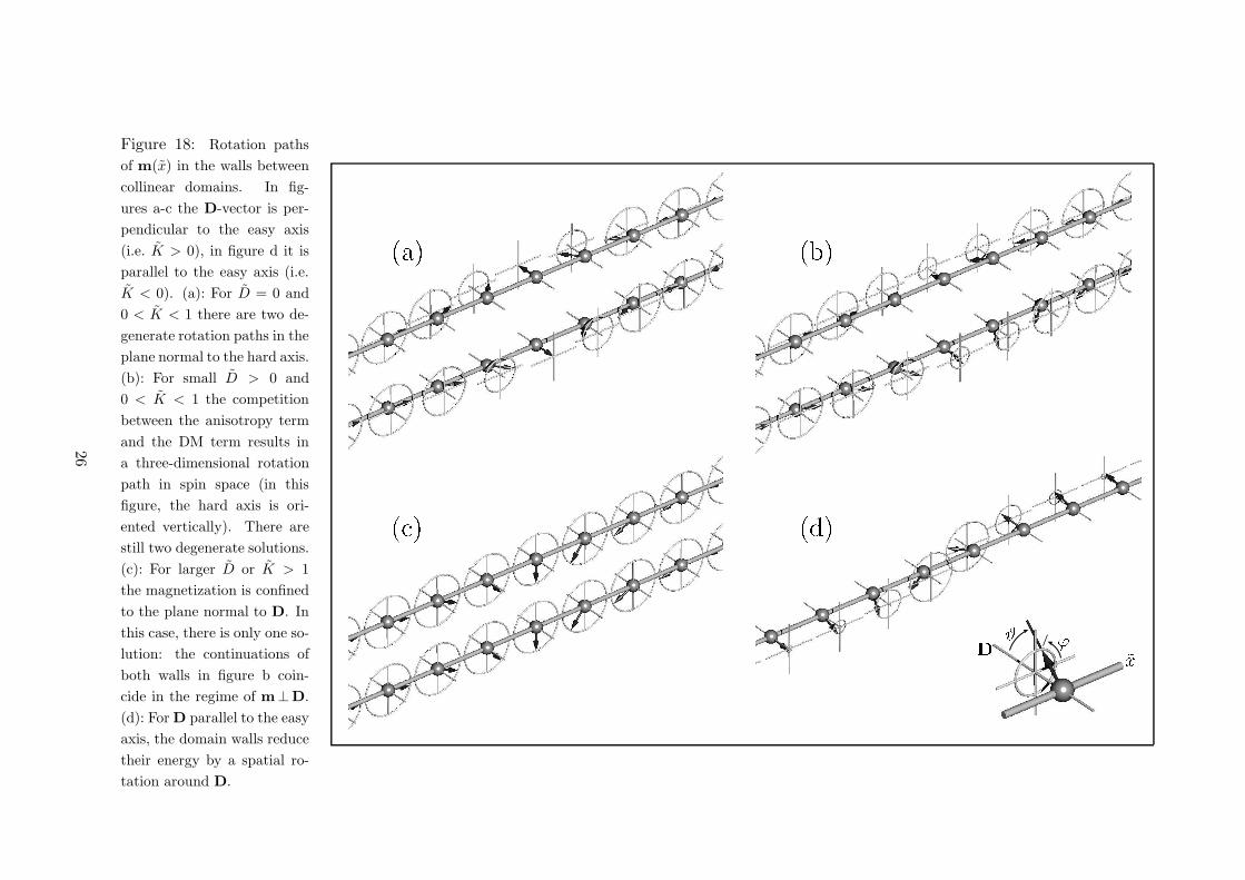
Figure 18: Rotation paths
of m(x) in the walls between
collinear domains. In fig-
ures a-c the D-vector is per-
pendicular to the easy axis
(i.e. K > 0), in figure d it is
parallel to the easy axis (i.e.
K < 0). (a): For D = 0 and
0 < K < 1 there are two de-
generate rotation paths in the
plane normal to the hard axis.
(b): For small D > 0 and
0 < K < 1 the competition
between the anisotropy term
and the DM term results in
a three-dimensional rotation
path in spin space (in this
figure, the hard axis is ori-
ented vertically). There are
still two degenerate solutions.
(c): For larger D or K > 1
the magnetization is confined
to the plane normal to D. In
this case, there is only one so-
lution: the continuations of
both walls in figure b coin-
cide in the regime of m⊥D.
(d): For D parallel to the easy
axis, the domain walls reduce
their energy by a spatial ro-
tation around D.
26

5 Dzyaloshinskii-Moriya interaction from first principles
5.1 DM-interaction within Multiple-Scattering Theory
Within multiple-scattering theory (MST) the DM constants Dij can be found in an elegant way,
as outlined in [47] and more recently in [48]. One employs the so-called “method of infinitesimal
rotations”, which provides the energy cost of an infinitesimal rotation of two spins, at sites i and
j, within second-order perturbation theory. An underlying assumption is that the associated
energy is related to the change of the single-particle energy levels only, i.e., one assumes again the
validity of the magnetic force theorem. The change in the single-particle levels is then calculated
in a straightforward way by utilizing Lloyd’s formula, in a way analogous to the derivation of the
Lichtenstein formula [10] for the Heisenberg exchange constants. Here, we follow the derivation
by Udvardi et al. [48]. It is implied that the spin-orbit coupling is already included in the
calculations of the electronic structure, scattering t-matrices, etc., before applying perturbation
theory for the infinitesimal rotations.
We distinguish between two models for the description of the solid, which we will then bring in
connection: (i) the density-functional model, including the charge and spin density ρ(r); m(r) at
each point as a degree of freedom, and giving rise to a free energy F [m; ρ]; and (ii) an extended,
classical Heisenberg-like model with a Hamiltonian H(Si), including spin-spin interactions up
to second order, and containing the directions of the magnetic moments at each atom, Si, as
degrees of freedom. It is assumed that, for the system properties in question, a mapping of the
free energy F of model (i) to the Hamiltonian H of model (ii) is meaningful. Such a mapping
leads obviously to a significant reduction of the degrees of freedom to the essential ones for the
problem at hand.
The spin-spin interaction can be described, up to second order, by the Hamiltonian
H =∑
i
K(Si) +∑
ij(i6=j)
SiJijSj (30)
Here, the first term describes the on-site anisotropy energy and the second term (where i 6= j)
includes the intersite exchange interactions and the Dzyaloshinskii-Moriya interaction. The
quantities Jij are 3 × 3 matrices (second rank tensors in real space). They can be decomposed
in symmetric and antisymmetric parts as:
Jij = Jij1 + JSij + JA
ij (31)
with Jij being the usual exchange interaction
Jij =1
3TrJij, (32)
JSij the (traceless) symmetric part
JSij =
1
2
(Jij + Jt
ij
)− Jij1, (33)
and JAij the antisymmetric part:
JAij =
1
2
(Jij − Jt
ij
). (34)
27

The latter can be brought in connection with the Dzyaloshinskii-Moriya interaction constants
Dij = (Dxij , D
yij , D
zij) by writing
JAij =
0 12(Jxy
ij − Jyxij ) 1
2(Jxzij − Jzx
ij )
−12(Jxy
ij − Jyxij ) 0 1
2 (Jyzij − J
zyij )
−12(Jxz
ij − Jzxij ) −1
2(Jyzij − J
zyij ) 0
=
0 Dzij −Dy
ij
−Dzij 0 Dx
ij
Dyij −Dx
ij 0
(35)
The spin-spin interaction is then written in terms of the Dzyaloshinskii-Moriya vectors as
SiJijSj = JijSiSj + SiJSijSj + Dij(Si × Sj) (36)
It is now necessary to express the interaction constants J xyij etc. in terms of H; then the sub-
stitution F ↔ H will make the connection to the density-functional model. We restrict the
discussion to the off-diagonal elements, as these enter expression (35) for the Dzyaloshinskii-
Moriya interaction. Evidently,
Jxyij =
∂2H
∂xi∂yj, (37)
and similar expressions hold for the other components. These can be rewritten in terms of
spherical coordinates (θi, φi) (defining the direction of magnetization Si). To obtain, for example,
the expression of J zyij in terms of H, it is convenient to choose a reference system in which the
magnetization of the ferromagnetic state is along the x-axis, as sketched in fig. 19. In this
reference system we get from eq. (30):
Jzyij = −
(∂2H
∂θi∂φj
)
θi,j=π2
φi,j=0
, Jyzij = −
(∂2H
∂φi∂θj
)
θi,j=π2
φi,j=0
, (38)
By choosing the magnetization along the y-axis, J xzij and Jzx
ij can be obtained as:
Jzxij = −
(∂2H
∂θi∂φj
)
θi,j=π2
φi,j=π2
, Jxzij =
(− ∂2H
∂φi∂θj
)
θi,j=π2
φi,j=π2
, (39)
while the Jxyij and Jyx
ij are found by placing the magnetization along the z-axis and taking
infinitesimal rotations in the x and y directions (thus we set θ = 0 and φ = 0, π2 ):
Jxyij =
(∂2H
∂θi∂θj
)θi,j=0φi=0φj=
π2
, Jyxij =
(∂2H
∂θi∂θj
)θi,j=0φi=
π2
φj=0
. (40)
We now turn to the expressions of the change of free energy with respect to infinitesimal rotations
of the magnetic moments within DFT, as derived by multiple-scattering theory. Again we follow
the derivation by Udvardi et al. [48]. The contribution of the single-particle levels to the free
energy at zero temperature is given in terms of the density of states n(E), or the integrated
density of states N(E) =∫ E
n(E′)dE′, as an integral up to the Fermi level EF :
F =
∫ EF
(E −EF )n(E)dE = −∫ EF
N(E)dE. (41)
By virtue of the magnetic force theorem, changes in the magnetization direction affect, to lowest
order, only this single-particle part of the free energy. Therefore, the change in total energy can
be directly associated with the changes in the integrated density of states.
28
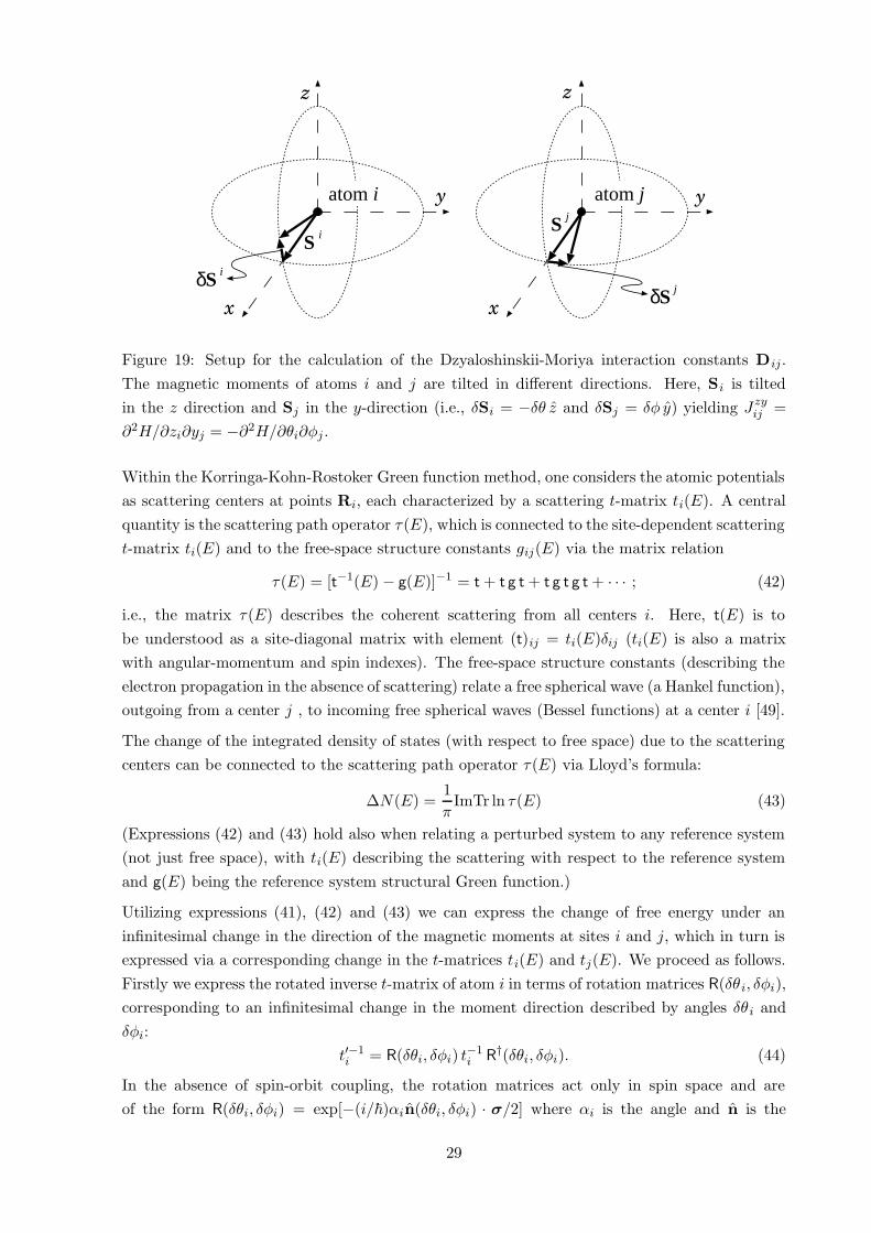
x
y
z
x
y
z
atom i atom j
S j
S i
δS i
δS j
Figure 19: Setup for the calculation of the Dzyaloshinskii-Moriya interaction constants Dij.
The magnetic moments of atoms i and j are tilted in different directions. Here, Si is tilted
in the z direction and Sj in the y-direction (i.e., δSi = −δθ z and δSj = δφ y) yielding J zyij =
∂2H/∂zi∂yj = −∂2H/∂θi∂φj .
Within the Korringa-Kohn-Rostoker Green function method, one considers the atomic potentials
as scattering centers at points Ri, each characterized by a scattering t-matrix ti(E). A central
quantity is the scattering path operator τ(E), which is connected to the site-dependent scattering
t-matrix ti(E) and to the free-space structure constants gij(E) via the matrix relation
τ(E) = [t−1(E) − g(E)]−1 = t + t g t + t g t g t + · · · ; (42)
i.e., the matrix τ(E) describes the coherent scattering from all centers i. Here, t(E) is to
be understood as a site-diagonal matrix with element (t)ij = ti(E)δij (ti(E) is also a matrix
with angular-momentum and spin indexes). The free-space structure constants (describing the
electron propagation in the absence of scattering) relate a free spherical wave (a Hankel function),
outgoing from a center j , to incoming free spherical waves (Bessel functions) at a center i [49].
The change of the integrated density of states (with respect to free space) due to the scattering
centers can be connected to the scattering path operator τ(E) via Lloyd’s formula:
∆N(E) =1
πImTr ln τ(E) (43)
(Expressions (42) and (43) hold also when relating a perturbed system to any reference system
(not just free space), with ti(E) describing the scattering with respect to the reference system
and g(E) being the reference system structural Green function.)
Utilizing expressions (41), (42) and (43) we can express the change of free energy under an
infinitesimal change in the direction of the magnetic moments at sites i and j, which in turn is
expressed via a corresponding change in the t-matrices ti(E) and tj(E). We proceed as follows.
Firstly we express the rotated inverse t-matrix of atom i in terms of rotation matrices R(δθi, δφi),
corresponding to an infinitesimal change in the moment direction described by angles δθi and
δφi:
t′−1i = R(δθi, δφi) t
−1i R†(δθi, δφi). (44)
In the absence of spin-orbit coupling, the rotation matrices act only in spin space and are
of the form R(δθi, δφi) = exp[−(i/~)αin(δθi, δφi) · σ/2] where αi is the angle and n is the
29
unit vector expressing the real-space rotation (δθi, δφi), and σ is the Pauli matrix vector; then
the equations are simplified, yielding the result of Lichtenstein for the exchange constants J ij
[10]. Here, however, spin-orbit coupling is present, so that the rotation affects also the angular
momentum part of the t-matrix; thus, R(δθi, δφi) = exp[−(i/~)αin(δθi, δφi) · (L + σ/2)], where
L is the angular momentum operator.
For the calculation of the exchange and DM-interactions we are interested in the change of
the free energy up to second order in δθi and δφi. Thus, the partial derivatives of the inverse
t-matrix are needed. These can be expressed via the derivatives of the rotation matrices (see
eq.(44)), as [48]:
t−1i θ ≡ ∂t−1
∂θi=∂R
∂θit−1i R† + R t−1
i
∂R†
∂θi(45)
t−1i φ ≡ ∂t−1
∂φi=∂R
∂φit−1i R† + R t−1
i
∂R†
∂φi(46)
Let us denote the change of t−1 due to the rotation of t−1i by δt−1
i (this matrix has non-zero
elements only at the (i, i) block). An infinitesimal rotation at sites i and j brings a change in
the scattering path operator,
τ ′ = [t−1 + δt−1i + δt−1
j − g]−1 = τ [1 + (δt−1i + δt−1
j ) τ ]−1. (47)
We are interested in the change of the integrated density of states caused by these rotations.
Having in mind Lloyd’s formula (43), we expand the logarithm of τ ′ up to second order:
δ ln τ = ln τ ′ − ln τ = 1 + (δt−1i + δt−1
j )− 1
2(δt−1
i + δt−1j ) τ (δt−1
i + δt−1j ) τ + · · · (48)
From equations (37-40) it is evident that we seek the quantity ∂2 ln τ/∂θi∂φj etc. Then only
the cross terms of the last part of eq. (48) survive, i.e., 12(δt−1
i τ δt−1j τ + δt−1
j τ δt−1i τ). Using
the cyclic property of the trace, we obtain
∂2
∂θi∂φjTr ln τ =
∂2
∂θi∂φjTr (t−1
i τ t−1j τ) = TrL t
−1i θ τij t
−1j φ τji, (49)
where in the last part the trace is only over angular momentum indexes (we have used the fact
that δt−1i has nonzero elements only in the (i, i)-block). Similar are the expressions for the other
partial second derivatives with respect to angles at both i and j. Combining this with Lloyd’s
formula (43) and with the free energy expression (42), we arrive at the following equations:
∂2F
∂φi∂φj= − 1
πIm
∫ EF
dE TrL[t−1i φ (E) τij(E) t−1
j φ(E) τji(E)] (50)
∂2F
∂θi∂φj= − 1
πIm
∫ EF
dE TrL[t−1i θ (E) τij(E) t−1
j φ(E) τji(E)] (51)
∂2F
∂θi∂θj= − 1
πIm
∫ EF
dE TrL[t−1i θ (E) τij(E) t−1
j θ (E) τji(E)] (52)
The final step is the connection of the two models (the Hamiltonian (30) and density-functional
theory) by making the substitution F → H in eqs. (50-52). Thus we arrive at expressions
30
describing the Dzyaloshinskii-Moriya interaction constants, using also equations (35) and (38-
40). We obtain:
Dxij = − 1
2πIm
∫ EF
dE TrL
[t−1i φ (E) τij(E) t−1
j θ (E) τji(E)− t−1i θ (E) τij(E) t−1
j φ(E) τji(E)]θi,j=
π2
φi,j=0
(53)
Dyij = − 1
2πIm
∫ EF
dE TrL
[−t−1
i φ (E) τij(E) t−1j θ (E) τji(E) + t−1
i θ (E) τij(E) t−1j φ(E) τji(E)
]θi,j=
π2
φi,j=π2
(54)
Dzij = − 1
2πIm
∫ EF
dE TrL
[t−1i θ (E) τij(E) t−1
j θ (E) τji(E)]θi,j=0φi=0φj=
π2
−[t−1i θ (E) τij(E) t−1
j θ (E) τji(E)]θi,j=0φi=
π2
φj=0
(55)
5.2 Calculating the DM interaction with periodic spin spirals
An alternative way to obtain model parameters like the elements of the above discussed matrix J ij
from first principles is to fit the energy expression obtained from the model ansatz to the
total energies obtained from electronic structure calculations for different magnetic states. We
follow this strategy in order to obtain the micromagnetic parameters that are discussed in
section 4. If we know the orientation of the Dzyaloshinskii vector from symmetry considerations,
we can constrain the magnetization to the plane normal to D and work with equation (22).
For homogeneous spin spirals (i.e. spirals with ϕ(x) = q = const or a constant canting angle
arccos(Si·Si+1) between the magnetizations of two adjacent lattice sites) the magnetic structure
has a period of λhs = 2π/q and the energy density E/λhs of the micromagnetic model gets
q
2πE(q) =
q
2π
2 πq∫
0
dx(Aq2 +D q +K sin2(q x)
)= Aq2 +D q + 1
2 K . (56)
Thus, we can obtain our model parameters A and D from a quadratic and a linear fit to
the dispersion curve q E(q) , with latter obtained from first-principles calculations. In order
to determine the anisotropy constant K, we can perform independent calculations of collinear
configurations with ϕ = 0 and ϕ = π .
Since the micromagnetic model is valid in the limit of slow spatial rotations, relation (56) holds
only for homogeneous spin spirals with large period lengths. This presents a formidable problem,
since the size of the unit cell that one can treat is limited by the computing facilities. We employ
a perturbative scheme in order to deal with these large magnetic superstructures: In contrast
to the method described in the previous section, we calculate the rotations selfconsistently
but treat the spin-orbit coupling as a perturbation. Thereby, we make use of the local force
31
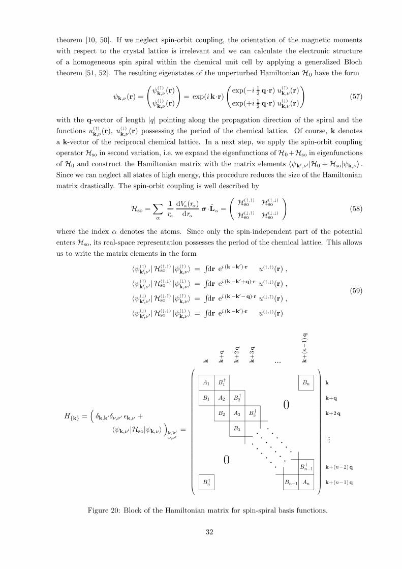
theorem [10, 50]. If we neglect spin-orbit coupling, the orientation of the magnetic moments
with respect to the crystal lattice is irrelevant and we can calculate the electronic structure
of a homogeneous spin spiral within the chemical unit cell by applying a generalized Bloch
theorem [51, 52]. The resulting eigenstates of the unperturbed Hamiltonian H0 have the form
ψk,ν(r) =
(ψ(↑)
k,ν(r)
ψ(↓)
k,ν(r)
)= exp(ik·r)
(exp(−i 1
2 q·r) u(↑)
k,ν(r)
exp(+i 12 q·r) u(↓)
k,ν(r)
)(57)
with the q-vector of length |q| pointing along the propagation direction of the spiral and the
functions u(↑)
k,ν(r), u(↓)
k,ν(r) possessing the period of the chemical lattice. Of course, k denotes
a k-vector of the reciprocal chemical lattice. In a next step, we apply the spin-orbit coupling
operator Hso in second variation, i.e. we expand the eigenfunctions of H0 +Hso in eigenfunctions
of H0 and construct the Hamiltonian matrix with the matrix elements 〈ψk′,ν′ |H0 +Hso|ψk,ν〉 .Since we can neglect all states of high energy, this procedure reduces the size of the Hamiltonian
matrix drastically. The spin-orbit coupling is well described by
Hso =∑
α
1
rα
dVα(rα)
drασ ·Lα =
(H(↑,↑)
so H(↑,↓)so
H(↓,↑)so H(↓,↓)
so
)(58)
where the index α denotes the atoms. Since only the spin-independent part of the potential
enters Hso, its real-space representation possesses the period of the chemical lattice. This allows
us to write the matrix elements in the form
〈ψ(↑)
k′,ν′ |H(↑,↑)so |ψ(↑)
k,ν〉 =∫dr ei (k−k′)·r u(↑,↑)(r) ,
〈ψ(↑)
k′,ν′ |H(↑,↓)so |ψ(↓)
k,ν〉 =∫dr ei (k−k′+q)·r u(↑,↓)(r) ,
〈ψ(↓)
k′,ν′ |H(↓,↑)so |ψ(↑)
k,ν〉 =∫dr ei (k−k′−q)·r u(↓,↑)(r) ,
〈ψ(↓)
k′,ν′ |H(↓,↓)so |ψ(↓)
k,ν〉 =∫dr ei (k−k′)·r u(↓,↓)(r)
(59)
Hk =(δk,k′δν,ν′ εk,ν +
〈ψk,ν′ |Hso|ψk,ν〉)
k,k′
ν,ν′
=
q
q
q
q
q
q
q
q
q
q
q
q
q
q
q
q
q
q
q
A1 B†1
B1 A2 B†2
B2 A3 B†3
B3
B†n−1
Bn−1 An
Bn
B †n
k k+
q
k+
2q
k+
3q
... k+
(n−
1)q
k
k+q
k+2q
...
k+(n−2)q
k+(n−1)q
0
0
Figure 20: Block of the Hamiltonian matrix for spin-spiral basis functions.
32
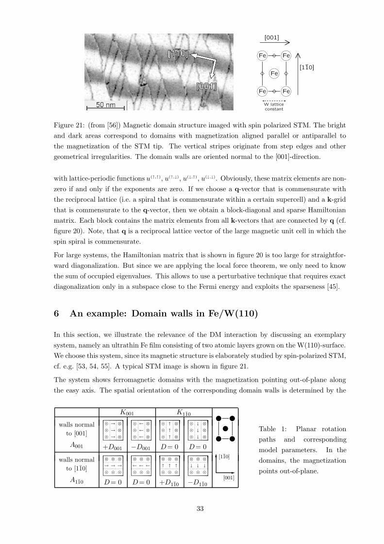
[110]
AA
[001]HH
Fe
Fe
Fe
Fe
Fe
-
W latticeconstant
Figure 21: (from [56]) Magnetic domain structure imaged with spin polarized STM. The bright
and dark areas correspond to domains with magnetization aligned parallel or antiparallel to
the magnetization of the STM tip. The vertical stripes originate from step edges and other
geometrical irregularities. The domain walls are oriented normal to the [001]-direction.
with lattice-periodic functions u(↑,↑), u(↑,↓), u(↓,↑), u(↓,↓). Obviously, these matrix elements are non-
zero if and only if the exponents are zero. If we choose a q-vector that is commensurate with
the reciprocal lattice (i.e. a spiral that is commensurate within a certain supercell) and a k-grid
that is commensurate to the q-vector, then we obtain a block-diagonal and sparse Hamiltonian
matrix. Each block contains the matrix elements from all k-vectors that are connected by q (cf.
figure 20). Note, that q is a reciprocal lattice vector of the large magnetic unit cell in which the
spin spiral is commensurate.
For large systems, the Hamiltonian matrix that is shown in figure 20 is too large for straightfor-
ward diagonalization. But since we are applying the local force theorem, we only need to know
the sum of occupied eigenvalues. This allows to use a perturbative technique that requires exact
diagonalization only in a subspace close to the Fermi energy and exploits the sparseness [45].
6 An example: Domain walls in Fe/W(110)
In this section, we illustrate the relevance of the DM interaction by discussing an exemplary
system, namely an ultrathin Fe film consisting of two atomic layers grown on the W(110)-surface.
We choose this system, since its magnetic structure is elaborately studied by spin-polarized STM,
cf. e.g. [53, 54, 55]. A typical STM image is shown in figure 21.
The system shows ferromagnetic domains with the magnetization pointing out-of-plane along
the easy axis. The spatial orientation of the corresponding domain walls is determined by the
K001 K110
z
z
z
z
z
-
6
[001]
[110]
walls normal
to [001]
A001
→
→
→
⊗
⊗
⊗
+D001
←
←
←
⊗
⊗
⊗
−D001
↑
↑
↑
⊗
⊗
⊗
D= 0
↓
↓
↓
⊗
⊗
⊗
D= 0
walls normal
to [110]
A110
→ → →
⊗ ⊗ ⊗
D= 0
← ← ←
⊗ ⊗ ⊗
D= 0
↑ ↑ ↑
⊗ ⊗ ⊗
+D110
↓ ↓ ↓
⊗ ⊗ ⊗
−D110
Table 1: Planar rotation
paths and corresponding
model parameters. In the
domains, the magnetization
points out-of-plane.
33
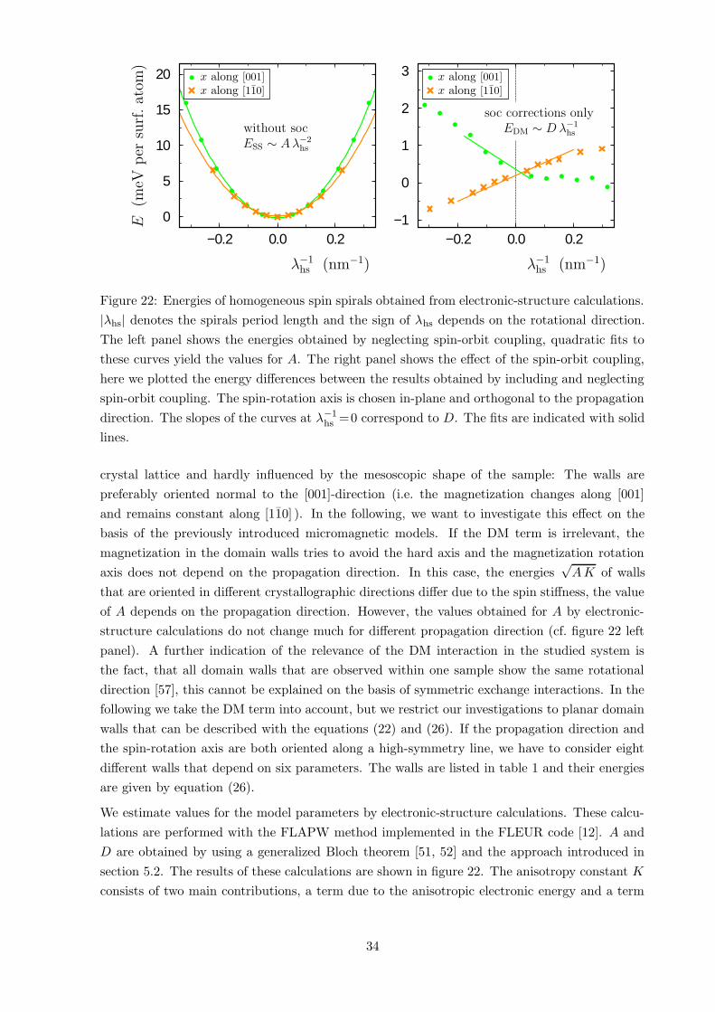
E(m
eVper
surf
.at
om)
−0.2 0.0 0.20
5
10
15
20
without socESS ∼ A λ
−2
hs
λ−1hs (nm−1)
x along [001]
x along [110]
−0.2 0.0 0.2−1
0
1
2
3
soc corrections onlyEDM ∼ D λ
−1
hs
λ−1hs (nm−1)
x along [001]
x along [110]
Figure 22: Energies of homogeneous spin spirals obtained from electronic-structure calculations.
|λhs| denotes the spirals period length and the sign of λhs depends on the rotational direction.
The left panel shows the energies obtained by neglecting spin-orbit coupling, quadratic fits to
these curves yield the values for A. The right panel shows the effect of the spin-orbit coupling,
here we plotted the energy differences between the results obtained by including and neglecting
spin-orbit coupling. The spin-rotation axis is chosen in-plane and orthogonal to the propagation
direction. The slopes of the curves at λ−1hs =0 correspond to D. The fits are indicated with solid
lines.
crystal lattice and hardly influenced by the mesoscopic shape of the sample: The walls are
preferably oriented normal to the [001]-direction (i.e. the magnetization changes along [001]
and remains constant along [110] ). In the following, we want to investigate this effect on the
basis of the previously introduced micromagnetic models. If the DM term is irrelevant, the
magnetization in the domain walls tries to avoid the hard axis and the magnetization rotation
axis does not depend on the propagation direction. In this case, the energies√AK of walls
that are oriented in different crystallographic directions differ due to the spin stiffness, the value
of A depends on the propagation direction. However, the values obtained for A by electronic-
structure calculations do not change much for different propagation direction (cf. figure 22 left
panel). A further indication of the relevance of the DM interaction in the studied system is
the fact, that all domain walls that are observed within one sample show the same rotational
direction [57], this cannot be explained on the basis of symmetric exchange interactions. In the
following we take the DM term into account, but we restrict our investigations to planar domain
walls that can be described with the equations (22) and (26). If the propagation direction and
the spin-rotation axis are both oriented along a high-symmetry line, we have to consider eight
different walls that depend on six parameters. The walls are listed in table 1 and their energies
are given by equation (26).
We estimate values for the model parameters by electronic-structure calculations. These calcu-
lations are performed with the FLAPW method implemented in the FLEUR code [12]. A and
D are obtained by using a generalized Bloch theorem [51, 52] and the approach introduced in
section 5.2. The results of these calculations are shown in figure 22. The anisotropy constant K
consists of two main contributions, a term due to the anisotropic electronic energy and a term
34
due to the magnetostatic interactions. The first term can be estimated directly from the elec-
tronic energies of collinear configurations with different spin quantization axes, the second term
can be estimated from the magnetic (dipole) moments Mj by applying the well-known formula
E(dip) =µ2
B
2
∑
j 6=0
(Mj ·M0)(Rj −R0)2 − 3((Rj −R0) ·Mj
)((Rj −R0) ·M0
)
|Rj −R0|5. (60)
This sum converges fast, since we are considering a two-dimensional ultrathin magnetic film
and not a magnetic bulk system. The results our calculations are summarized in table 2 (for
computational details cf. [45]). The values given for the spin-stiffness constants A are fairly
accurate, since they are obtained from an unambiguous fitting procedure on a curve on a large
energy scale (cf. figure 22). The values given for D are less accurate, but they tell us the order
of magnitude of the Dzyaloshinskii vector. The accuracy of the anisotropy constants K is not
satisfactory, these calculations reach the limit of our computational method and we cannot rule
out an error of a few meV nm−1 (note that 1 meV nm−2 = 0.035 meV per Fe atom ).
001 110
spin stiffness A / ( meV ) 56.4 44.8
DM interaction D / ( meV nm−1 ) −10.4 7.3
anisotropy energy K / ( meV nm−2 ) 1.1 2.3
Table 2: Theoretically predicted model parameters converted into areal densities. The crystal-
lographic directions refer to the indices used in table 1.
Inserting the values given in table 2 in equation (26) yields the wall energies
4√A001K001 − π |D001| = −1.2 meV nm−1 ,
4√A001 K110 = 45.6 meV nm−1 ,
4√A110K001 = 28.1 meV nm−1 ,
4√A110K110 − π |D110| = 17.7 meV nm−1 .
(61)
A negative wall energy indicates that a rotating spin structure is energetically more favorable
than a collinear state. From the results (61) we would predict a spiral propagating along the
[001]-direction, thus we would not only explain the experimentally observed domain-wall ori-
entation but also the formation of the regular domain pattern. However, due to the large
uncertainties in the values and the restriction to planar spin structures, the good agreement
with the experiment may be supported by an accidental cancellation of errors. Nevertheless,
the calculations clearly show two points: The observed wall orientation cannot be explained
by the spin stiffness alone, and the DM interaction is strong enough to compete with the other
quantities. Keeping in mind that all domain walls show the same rotational direction, the DM in-
teraction presents the most plausible explanation for the observed mesoscale magnetic structure.
The studied system nicely illustrates the relevance of the Dzyaloshinskii-Moriya interactions for
magnetic surfaces.
35

Acknowledgements
We want to thank E. Chulkov and Th. Schapers for stimulating discussions and acknowledge
financial support from Deutsche Forschunsgemeinschaft (DFG) grant No. BI 823/1.
References
[1] M. N. Baibich, J. M. Broto, A. Fert, F. N. V. Dau, F. Petroff, P. Eitenne, G. Creuzet,
A. Friederich, and J. Chazelas, Giant magnetoresistance of (001)Fe/(001)Cr magnetic
superlattices, Phys. Rev. Lett. 61, 2472 (1988).
[2] G. Binash, P. Grunberg, F. Saurenbach, and W. Zinn, Enhanced magnetoresistance in
layered magnetic structures with antiferromagnetic interlayer exchange, Phys. Rev. B 39,
4828 (1989).
[3] S. A. Wolf, D. D. Awschalom, R. A. Buhrman, J. M. Daughton, S. von Molnar, M. L.
Roukes, A. Y. Chtchelkanova, and D. M. Treger, Spintronics: A spin-based electronic
vision for the future, Science 294, 1488 (2001).
[4] I. Zutc, J. Fabian, and S. D. Sarma, Spintronics: Fundamentals and applications, Rev.
Mod. Phys. 76, 323 (2004).
[5] E. I. Rashba, Properties of semiconductors with an extremum loop, Sov. Phys. Solid State
2, 1109 (1960).
[6] S. Datta and B. Das, Electronic analog of the electro-optic modulator, Appl. Phys. Lett.
56, 665 (1990).
[7] W. Heisenberg, Zur Theorie des Ferromagnetismus, Z. f. Physik 49, 619 (1928).
[8] I. E. Dzialoshinskii, Thermodynamic Theory of ”Weak” Ferromagnetism In Antiferromag-
netic Substances, Sov. Phys. JETP 5, 1259 (1957).
[9] T. Moriya, Anisotropic Superexchange Interaction and Weak Ferromagnetism, Physical
Review 120, 91–98 (1960).
[10] A. I. Liechtenstein, M. I. Katsnelson, V. P. Antropov, and V. A. Gubanov, Local spin
density functional approach to the theory of exchange interactions in ferromagnetic metals
and alloys, J. Magn. Magn. Mater. 67, 65 (1987).
[11] E. Wimmer, H. Krakauer, M. Weinert, and A. Freeman, Full-potential self-consistent
linearized-augmented-plane-wave method for calculating the electronic structure of
molecules and surfaces: O2 molecule, Phys. Rev. B 24, 864 (1981).
[12] For program description see http://www.flapw.de.
[13] C. Li, A. J. Freeman, H. J. F. Jansen, and C. L. Fu, Magnetic anisotropy in low-dimensional
ferromagnetic systems: Fe monolayers on Ag(001), Au(001), and Pd(001) substrates, Phys.
Rev. B 42, 5433 (1990).
36

[14] P. Kurz, F. Forster, L. Nordstrom, G. Bihlmayer, and S. Blugel, Ab initio treatment of non-
collinear magnets with the full-potential linearized augmented planewave method, Phys.
Rev. B 69, 024415 (2004).
[15] T. Schapers, J. Knobbe, and V. A. Guzenko, Effect of Rashba spin-orbit coupling on mag-
netotransport in InGaAs/InP quantum wire structures, Phys. Rev. B 69, 235323 (2004).
[16] Y. A. Bychkov and E. I. Rashba, Oscillatory effects and the magnetic-susceptibility of
carriers in inversion-layers, J. Phys. C 17, 6039 (1984).
[17] Y. A. Bychkov and E. I. Rashba, Properties of a 2D electron-gas with lifted spectral
degeneracy, Sov. Phys. JETP Lett 39, 78 (1984).
[18] R. Winkler, Rashba splitting in two-dimensional electron and hole systems, Phys. Rev. B
62, 4245 (2000).
[19] G. Dresselhaus, Spin-orbit coupling effects in zinc blende structures, Phys. Rev. 100, 580
(1955).
[20] V. A. Guzenko, J. Knobbe, H. Hardtdegen, T. Schapers, and A. Bringer, Rashba effect in
InGaAs/InP parallel quantum wires, Appl. Phys. Lett. 88, 032102 (2006).
[21] J. Wrobel, T. Dietl, A. Lusakowski, G. Grabecki, K. Fronc, R. Hey, K. H. Ploog, and
H. Shtrikman, Spin Filtering in a Hybrid Ferromagnetic-Semiconductor Microstructure,
Phys. Rev. Lett. 93, 246601 (2004).
[22] S. LaShell, B. A. McDougall, and E. Jensen, Spin Splitting of an Au(111) Surface State
Band Observed with Angle Resolved Photoelectron Spectroscopy, Phys. Rev. Lett. 77,
3419 (1996).
[23] M. Hoesch, M. Muntwiler, V. N. Petrov, M. Hengsberger, L. Patthey, M. Shi, M. Falub,
T. Greber, and J. Osterwalder, Spin structure of the Shockley surface state on Au(111),
Phys. Rev. B 69, 241401(R) (2004).
[24] J. Henk, A. Ernst, and P. Bruno, Spin polarization of the L-gap surface states on Au(111),
Phys. Rev. B 68, 165416 (2003).
[25] G. Nicolay, F. Reinert, S. Hufner, and P. Blaha, Spin-orbit splitting of the L-gap surface
state on Au(111) and Ag(111), Phys. Rev. B 65, 033407 (2001).
[26] G. Bihlmayer, Y. M. Koroteev, P. M. Echenique, E. V. Chulkov, and S. Blugel, The
Rashba-effect at metallic surfaces, Surf. Sci. 600, 3888 (2006).
[27] L. Petersen and P. Hedegard, A simple tight-binding model of spin-orbit splitting of sp-
derived surface states, Surf. Sci. 459, 49 (2000).
[28] S. Agergaard, C. Søndergaard, H. Li, M. B. Nielsen, S. V. Hoffmann, Z. Li, and P. Hofmann,
The effect of reduced dimensionality on a semimetal: the electronic structure of the Bi(110)
surface, New J. Phys. 3, 15 (2001).
37

[29] J. Sun, A. Mikkelsen, M. F. Jensen, Y. M. Koroteev, G. Bihlmayer, E. V. Chulkov, D. L.
Adams, P. Hofmann, and K. Pohl, Structural determination of the Bi(110) semimetal
surface by LEED analysis and ab initio calculations, Phys. Rev. B 74, accepted (2006).
[30] C. R. Ast and H. Hochst, Fermi surface of Bi(111) measured by photoemission spectroscopy,
Phys. Rev. Lett. 87, 177602 (2001).
[31] H. Monig, J. Sun, Y. M. Koroteev, G. Bihlmayer, E. V. Chulkov, K. Pohl, and P. Hofmann,
The structure of the (111) surface of bismuth, Phys. Rev. B 72, 085410 (2005).
[32] J. I. Pascual, G. Bihlmayer, Y. M. Koroteev, H.-P. Rust, G. Ceballos, M. Hansmann,
K. Horn, E. V. Chulkov, S. Blugel, P. M. Echenique, and P. Hofmann, The role of the spin
in quasiparticle interference, Phys. Rev. Lett. 93, 196802 (2004).
[33] P. Hofmann, J. E. Gayone, G. Bihlmayer, Y. M. Koroteev, and E. V. Chulkov, Electronic
structure and Fermi surface of Bi(100), Phys. Rev. B 71, 195413 (2005).
[34] Y. M. Koroteev, G. Bihlmayer, J. E. Gayone, E. V. Chulkov, S. Blugel, P. M. Echenique,
and P. Hofmann, Strong spin-orbit splitting on Bi surfaces, Phys. Rev. Lett. 93, 046403
(2004).
[35] C. R. Ast and H. Hochst, Indication of charge-density-wave formation in Bi(111),
Phys. Rev. Lett. 90, 016403 (2003).
[36] T. Hirahara, T. Nagao, I. Matsuda, G. Bihlmayer, E. V. Chulkov, Y. M. Koroteev, P. M.
Echenique, M. Saito, and S. Hasegawa, Role of spin-orbit coupling and hybridization effects
in the electronic structure of ultrathin Bi films, Phys. Rev. Lett. 97, 146803 (2006).
[37] O. Krupin, G. Bihlmayer, K. Starke, S. Gorovikov, J. E. Prieto, K. Dobrich, S. Blugel, and
G. Kaindl, Rashba effect at magnetic metal surfaces, Phys. Rev. B 71, 201403 (R) (2005).
[38] D. A. Smith, New mechanisms for magnetic anisotropy in localised s-state moment mate-
rials, J. Magn. Magn. Mater. 1, 214 (1976).
[39] A. Fert and P. M. Levy, Role of Anisotropic Exchange Interactions in Determining the
Properties of Spin-Glasses, Phys. Rev. Lett. 44, 1538 (1980).
[40] U. K. Roßler, A. N. Bogdanov, and C. Pfleiderer, Spontaneous skyrmion ground states in
magnetic metals, Nature 442, 797 (2006).
[41] C. Kittel, Physical Theory of Ferromagnetic Domains, Rev. Mod. Phys. 49, 541 (1949).
[42] I. E. Dzyaloshinskiı, Theory of helicoidal structures in antiferromagnets. III., Sov. Phys.
JETP 20, 665 (1965).
[43] Yu. A. Izyumov, Modulated, or long-periodic, magnetic structures of crystals, Sov. Phys.
Usp. 27, 845 (1984).
[44] L. Landau and E. Lifshitz, On the Theory of the Dispersion of Magnetic Permeability in
Ferromagnetic Bodies, Phys. Z. Sowjetunion 8, 153 (1935).
38
[45] M. Heide, Magnetic domain walls in ultrathin films: Contribution of the Dzyaloshinsky-
Moriya interaction, PhD Thesis, RWTH Aachen, Germany, 2006.
[46] M. Heide, G. Bihlmayer, and S. Blugel, to be published.
[47] J. B. Staunton, B. L. Gyorffy, J. Poulter, and P. Strange, A relativistic RKKY interaction
between two magnetic impurities-the origin of a magnetic anisotropic effect, J. Phys. C:
Solid State Phys. 21, 1595 (1988).
[48] L. Udvardi, L. Szunyogh, K. Palotas, and P. Weinberger, First-principles relativistic study
of spin waves in thin magnetic films, Phys. Rev. B 68, 104436 (2002).
[49] A. Gonis, Theoretical Materials Science, Materials Research Society, 2000.
[50] A. R. Mackintosh and O. K. Andersen, Electrons at the Fermi Surface, page 149, ed.
M. Springford, Cambridge Univ. Press, London, 1980.
[51] C. Herring, Exchange interactions among intinerant electrons, Magnetism Vol. IV, ed.
G. T. Rado, H. Suhl, Academic Press, New York, London, 1966.
[52] L. M. Sandratskii, Symmetry analysis of electronic states for crystals with spiral magnetic
order. I. General properties, J. Phys.: Condens. Matter 3, 8565 (1991).
[53] M. Pratzer, H. J. Elmers, M. Bode, O. Pietzsch, A. Kubetzka, and R. Wiesendanger,
Atomic-scale magnetic domain walls in quasi-one-dimensional Fe nanostripes, Phys. Rev.
Lett. 87, 127201 (2001).
[54] M. Bode, Spin-polarized scanning tunneling microscopy, Rep. Prog. Phys. 66, 523 (2003).
[55] E. Y. Vedmedenko, A. Kubetzka, K. von Bergmann, O. Pietzsch, M. Bode, J. Kirschner,
H. P. Oepen, and R. Wiesendanger, Domain Wall Orientation in Magnetic Nanowires,
Phys. Rev. Lett. 92, 77207 (2004).
[56] K. von Bergmann, Iron nanostructures studied by spin-polarized scanning tunneling mi-
croscopy, PhD Thesis, Universitat Hamburg, Germany, 2004.
[57] O. Pietzsch, Magnetic Imaging by Spin-Polarized Scanning Tunneling Spectroscopy Applied
to Ultrathin Fe/W(110) Films, PhD Thesis, Universitat Hamburg, Germany, 2001.
39