1 MTD Readout Electronics J. Schambach University of Texas Hefei, March 2011.
23
1 MTD Readout Electronics J. Schambach University of Texas Hefei, March 2011
-
Upload
paul-holland -
Category
Documents
-
view
213 -
download
0
Transcript of 1 MTD Readout Electronics J. Schambach University of Texas Hefei, March 2011.

1
MTD Readout Electronics
J. Schambach
University of Texas
Hefei, March 2011

2
TOF Electronics Overview

The same as TOF, mostly…
• THUB, TCPU, TDIG are identical– Each TCPU reads out 3 or 5 TDIG (1 backleg)
• MINO is a 4-NINO version of TINO– Each MTD tray gets 1 MINO & 1 TDIG
• MTRG – this is a new card; it combines the NINO trigger outputs logically and sends a signal to trigger: the earliest east-end and west-end signal for each backleg
• MFTB – a new un-powered board that “closes” the gas box (tray) and passes the MRPC signals to MINO
• There are 2 THUB, 28 TCPU, 118 TDIG, 118 MINO, and 28 MTRG boards in the MTD electronics
3

MTD Electronics Overview
4
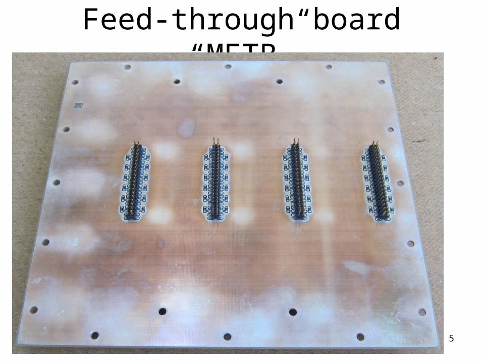
Feed-through board “MFTB”
5

6
Front-End Electronics “TINO”TINO
NINO C
NINO B
NINO A(8 ch Amp / Disc)
MRPC 4(6 ch)
MRPC 1(6 ch)
MRPC 3(6 ch)
MRPC 2(6 ch)
Multiplicity to TDIG PLD(1 bit LVDS)
Hits to HPDTC(8 LVDS)
Threshold(All Common from TDIG)
MR
PC
Inte
rfac
eM
RP
C In
terf
ace
MR
PC
Inte
rfac
eM
RP
C In
terf
ace
6
6
6
6
6
6
2
4
4
2
8
8
TD
IG Interface
TD
IG Interface
TD
IG Interface

MINO (“MTD TINO”)
7

8
CERN/LAA NINO Chipdeveloped for ALICE
Parameter Value
Peaking time 1ns
Signal Range 100fC – 2pC
Noise (with detector) < 5000 e- rms
Front edge time jitter <25ps rms
Power consumption 30 mW/ch
Discriminator threshold 10fC to 100fC
Differential Input impedance 40Ω< Zin < 75Ω
Output interface LVDS

MINO
9

10
Digitizer Board “TDIG”

TDIG
11

12
HPTDC: Data driven TDC• Only stores data when hit detected• Variable latency over full (1/4) dynamic range
Compromise between hit rate and latency• Triggered / non triggered mode• Multiple overlapping triggers• Channel merging possible via derandomizers
Limits hit rates• Good double pulse resolution
But complicated dead time analysis• Buffer occupancies must be seriously analyzed• Buffer overflows must be handled carefully
– Hit may be lost if marked– Complete events must never be lost
• Wide latency buffer (covers full dynamic range)• More complicated architecture/implementation
Previous data driven TDC worked well in different applications– Logic complication handled by logic synthesis– Extended verifications at behavioral/register/gate
level• High flexibility
Large dynamic range
FIFO orDual port RAM
Hit
Triggertime tag
Compare time
OutputFIFO
Trigger
-
Latency
Derandomizer FIFO’s
Common FIFO

13
HPTDC Time Measurement
Coarse time(bin width 25 ns, 11 bits)
PLL bits(bin width 3.125 ns)
DLL bits(bin width 98 ps)
MSB LSB
R-C bits(bin width 24.4 ps)
HPTDC is fed by a 40 MHz clock giving us a basic 25 ns period (coarse count).
A PLL (Phase Locked Loop) device inside the chip does clock multiplication by a factor 8 (3 bits) to 320 MHz (3.125 ns period) .
A DLL (Delay Locked Loop) done by 32 cells fed by the PLL clock acts as a 5 bit hit register for each PLL clock (98 ps width LSB = 3.125 ns/32).
4 R-C delay lines divide each DLL bin in 4 parts (R-C interpolation)

14
HPTDC Buffering & Readout
Level-0 Trigger
BunchCrossing Hit Buffer
Level-0Buffering
8 channel @ 25ps
or
32 channels @ 100ps

15
Tray Controller “TCPU”

TCPU
16

MTRG
17

18
DAQ/Trigger Interface THUB
National’s SerDes Chip

ALICE DDL Link
J. Schambach 19
Front-end electronicsFront-end electronics
DetectorData Link
DDL SIUDDL SIU
DDL DIUDDL DIU
RORCRORC
SourceInterfaceUnit
DestinationInterfaceUnit
ReadOutReceiver Card
PCPCData
Acquisition PC
Optical Fibre~200 meters
PCI

THUB
DOE Review Aug 10/11 2009
J. Schambach 20

Electronics Monitoring & Configuration Tool
J. Schambach 21

Global System Clock Distribution
22

HPTDC Readout Paths
23