
1 Mbit / 2 Mbit / 4 Mbit (x8) Multi-Purpose Flash...
28
©2012 Silicon Storage Technology, Inc. DS25023B 06/13 Data Sheet www.microchip.com 1 Mbit / 2 Mbit / 4 Mbit (x8) Multi-Purpose Flash SST39LF010 / SST39LF020 / SST39LF040 SST39VF010 / SST39VF020 / SST39VF040 Features • Organized as 128K x8 / 256K x8 / 512K x8 • Single Voltage Read and Write Operations – 3.0-3.6V for SST39LF010/020/040 – 2.7-3.6V for SST39VF010/020/040 • Superior Reliability – Endurance: 100,000 Cycles (typical) – Greater than 100 years Data Retention • Low Power Consumption (typical values at 14 MHz) – Active Current: 5 mA (typical) – Standby Current: 1 μA (typical) • Sector-Erase Capability – Uniform 4 KByte sectors • Fast Read Access Time: – 55 ns for SST39LF010/020/040 – 70 ns for SST39VF010/020/040 • Latched Address and Data • Fast Erase and Byte-Program: – Sector-Erase Time: 18 ms (typical) – Chip-Erase Time: 70 ms (typical) – Byte-Program Time: 14 μs (typical) – Chip Rewrite Time: 2 seconds (typical) for SST39LF/VF010 4 seconds (typical) for SST39LF/VF020 8 seconds (typical) for SST39LF/VF040 • Automatic Write Timing – Internal V PP Generation • End-of-Write Detection – Toggle Bit – Data# Polling • CMOS I/O Compatibility • JEDEC Standard – Flash EEPROM Pinouts and command sets • Packages Available – 32-lead PLCC – 32-lead TSOP (8mm x 14mm) • All devices are RoHS compliant The SST39LF010, SST39LF020, SST39LF040 and SST39VF010, SST39VF020, SST39VF040 are 128K x8, 256K x8 and 5124K x8 CMOS Multi-Purpose Flash (MPF) manufactured with SST’s proprietary, high performance CMOS SuperFlash technology. The split-gate cell design and thick-oxide tunneling injector attain bet- ter reliability and manufacturability compared with alternate approaches. The SST39LF010/020/040 devices write (Program or Erase) with a 3.0-3.6V power supply. The SST39VF010/020/040 devices write with a 2.7-3.6V power supply. The devices conform to JEDEC standard pinouts for x8 memories.
Transcript of 1 Mbit / 2 Mbit / 4 Mbit (x8) Multi-Purpose Flash...
©2012 Silicon Storage Technology, Inc. DS25023B 06/13
Data Sheet
www.microchip.com
1 Mbit / 2 Mbit / 4 Mbit (x8) Multi-Purpose FlashSST39LF010 / SST39LF020 / SST39LF040
SST39VF010 / SST39VF020 / SST39VF040
Features• Organized as 128K x8 / 256K x8 / 512K x8
• Single Voltage Read and Write Operations– 3.0-3.6V for SST39LF010/020/040– 2.7-3.6V for SST39VF010/020/040
• Superior Reliability– Endurance: 100,000 Cycles (typical)– Greater than 100 years Data Retention
• Low Power Consumption(typical values at 14 MHz)
– Active Current: 5 mA (typical)– Standby Current: 1 µA (typical)
• Sector-Erase Capability– Uniform 4 KByte sectors
• Fast Read Access Time:– 55 ns for SST39LF010/020/040– 70 ns for SST39VF010/020/040
• Latched Address and Data
• Fast Erase and Byte-Program:– Sector-Erase Time: 18 ms (typical)– Chip-Erase Time: 70 ms (typical)– Byte-Program Time: 14 µs (typical)– Chip Rewrite Time:
2 seconds (typical) for SST39LF/VF0104 seconds (typical) for SST39LF/VF0208 seconds (typical) for SST39LF/VF040
• Automatic Write Timing– Internal VPP Generation
• End-of-Write Detection– Toggle Bit– Data# Polling
• CMOS I/O Compatibility
• JEDEC Standard– Flash EEPROM Pinouts and command sets
• Packages Available– 32-lead PLCC– 32-lead TSOP (8mm x 14mm)
• All devices are RoHS compliant
The SST39LF010, SST39LF020, SST39LF040 and SST39VF010, SST39VF020,SST39VF040 are 128K x8, 256K x8 and 5124K x8 CMOS Multi-Purpose Flash(MPF) manufactured with SST’s proprietary, high performance CMOS SuperFlashtechnology. The split-gate cell design and thick-oxide tunneling injector attain bet-ter reliability and manufacturability compared with alternate approaches. TheSST39LF010/020/040 devices write (Program or Erase) with a 3.0-3.6V powersupply. The SST39VF010/020/040 devices write with a 2.7-3.6V power supply.The devices conform to JEDEC standard pinouts for x8 memories.
©2012 Silicon Storage Technology, Inc. DS25023B 06/13
2
1 Mbit / 2 Mbit / 4 Mbit Multi-Purpose FlashSST39LF010 / SST39LF020 / SST39LF040
SST39VF010 / SST39VF020 / SST39VF040
Data Sheet
Product DescriptionThe SST39LF010, SST39LF020, SST39LF040 and SST39VF010, SST39VF020, SST39VF040 are128K x8, 256K x8 and 5124K x8 CMOS Multi-Purpose Flash (MPF) manufactured with SST’s proprie-tary, high performance CMOS SuperFlash technology. The split-gate cell design and thick-oxide tun-neling injector attain better reliability and manufacturability compared with alternate approaches. TheSST39LF010/020/040 devices write (Program or Erase) with a 3.0-3.6V power supply. TheSST39VF010/020/040 devices write with a 2.7-3.6V power supply. The devices conform to JEDECstandard pinouts for x8 memories.
Featuring high performance Byte-Program, the SST39LF010/020/040 and SST39VF010/020/040devices provide a maximum Byte-Program time of 20 µsec. These devices use Toggle Bit or Data#Polling to indicate the completion of Program operation. To protect against inadvertent write, they haveon-chip hardware and Software Data Protection schemes. Designed, manufactured, and tested for awide spectrum of applications, they are offered with a guaranteed typical endurance of 100,000 cycles.Data retention is rated at greater than 100 years.
The SST39LF010/020/040 and SST39VF010/020/040 devices are suited for applications that requireconvenient and economical updating of program, configuration, or data memory. For all system appli-cations, they significantly improves performance and reliability, while lowering power consumption.They inherently use less energy during Erase and Program than alternative flash technologies. Thetotal energy consumed is a function of the applied voltage, current, and time of application. Since forany given voltage range, the SuperFlash technology uses less current to program and has a shortererase time, the total energy consumed during any Erase or Program operation is less than alternativeflash technologies. These devices also improve flexibility while lowering the cost for program, data, andconfiguration storage applications.
The SuperFlash technology provides fixed Erase and Program times, independent of the number ofErase/Program cycles that have occurred. Therefore the system software or hardware does not haveto be modified or de-rated as is necessary with alternative flash technologies, whose Erase and Pro-gram times increase with accumulated Erase/Program cycles.
To meet surface mount requirements, the SST39LF010/020/040 and SST39VF010/020/040 devicesare offered in 32-lead PLCC and 32-lead TSOP packages. See Figures 2 and 3 for pin assignments.
©2012 Silicon Storage Technology, Inc. DS25023B 06/13
3
1 Mbit / 2 Mbit / 4 Mbit Multi-Purpose FlashSST39LF010 / SST39LF020 / SST39LF040
SST39VF010 / SST39VF020 / SST39VF040
Data Sheet
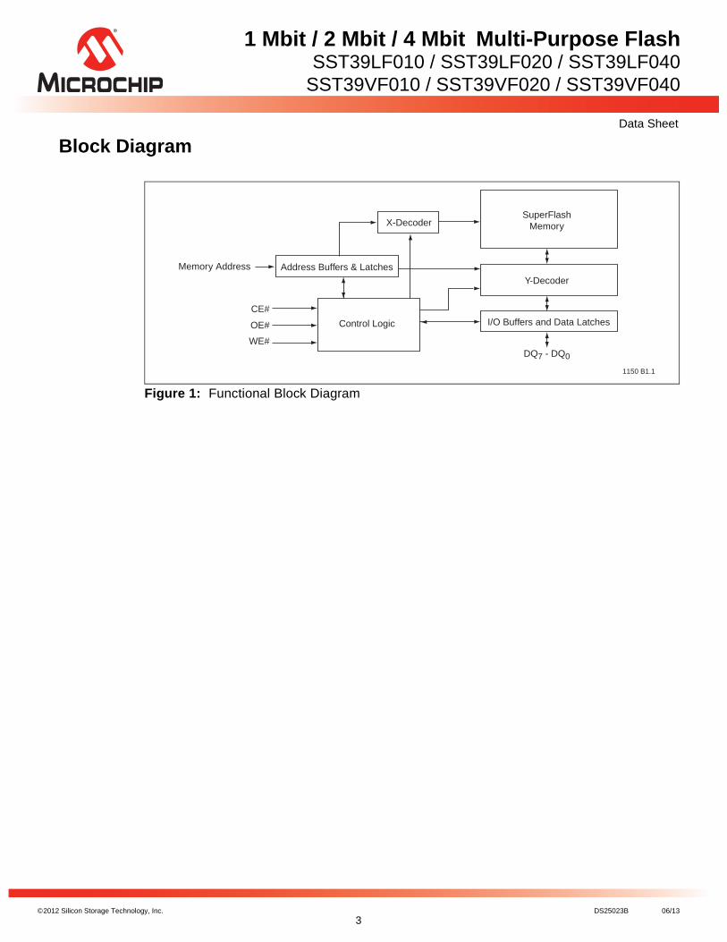
Block Diagram
Figure 1: Functional Block Diagram
Y-Decoder
I/O Buffers and Data Latches
1150 B1.1
Address Buffers & Latches
X-Decoder
DQ7 - DQ0
Memory Address
OE#
CE#
WE#
SuperFlashMemory
Control Logic

©2012 Silicon Storage Technology, Inc. DS25023B 06/13
4
1 Mbit / 2 Mbit / 4 Mbit Multi-Purpose FlashSST39LF010 / SST39LF020 / SST39LF040
SST39VF010 / SST39VF020 / SST39VF040
Data Sheet
Pin Assignments
Figure 2: Pin Assignments for 32-lead PLCC
5
6
7
8
9
10
11
12
13
29
28
27
26
25
24
23
22
21
A7
A6
A5
A4
A3
A2
A1
A0
DQ0
A7
A6
A5
A4
A3
A2
A1
A0
DQ0
A7
A6
A5
A4
A3
A2
A1
A0
DQ0
A14
A13
A8
A9
A11
OE#
A10
CE#
DQ7
A14
A13
A8
A9
A11
OE#
A10
CE#
DQ7
A14
A13
A8
A9
A11
OE#
A10
CE#
DQ7
4 3 2 1 32 31 30A
12
A15
A16
NC
VD
D
WE
#
NC
A12
A15
A16
NC
VD
D
WE
#
A17
A12
A15
A16
A18
VD
D
WE
#
A17
32-lead PLCCTop View
1150 32-plcc NH P4.4
14 15 16 17 18 19 20
DQ
1
DQ
2
VS
S
DQ
3
DQ
4
DQ
5
DQ
6
DQ
1
DQ
2
VS
S
DQ
3
DQ
4
DQ
5
DQ
6
DQ
1
DQ
2
VS
S
DQ
3
DQ
4
DQ
5
DQ
6
SST39LF/VF010SST39LF/VF020SST39LF/VF040 SST39LF/VF010 SST39LF/VF020 SST39LF/VF040SS
T39L
F/VF
010
SST3
9LF/
VF02
0SS
T39L
F/VF
040
SST3
9LF/
VF01
0SS
T39L
F/VF
020
SST3
9LF/
VF04
0

©2012 Silicon Storage Technology, Inc. DS25023B 06/13
5
1 Mbit / 2 Mbit / 4 Mbit Multi-Purpose FlashSST39LF010 / SST39LF020 / SST39LF040
SST39VF010 / SST39VF020 / SST39VF040
Data Sheet
Figure 3: Pin Assignments for 32-lead TSOP (8mm x 14mm)
Table 1: Pin DescriptionSymbol Pin Name FunctionsAMS
1-A0
1. AMS = Most significant addressAMS = A16 for SST39LF/VF010, A17 for SST39LF/VF020, and A18 for SST39LF/VF040
Address Inputs To provide memory addresses. During Sector-Erase AMS-A12 address lines will select the sector. During Block-Erase AMS-A16 address lines will select the block.
DQ7-DQ0 Data Input/output To output data during Read cycles and receive input data during Write cycles.Data is internally latched during a Write cycle.The outputs are in tri-state when OE# or CE# is high.
CE# Chip Enable To activate the device when CE# is low.OE# Output Enable To gate the data output buffers.
WE# Write Enable To control the Write operations.
VDD Power Supply To provide power supply voltage: 3.0-3.6V for SST39LF010/020/0402.7-3.6V for SST39VF010/020/040
VSS GroundNC No Connection Unconnected pins.
T1.1 25023
A11A9A8
A13A14NC
WE#VDD
NCA16A15A12
A7A6A5A4
A11A9A8
A13A14A17
WE#VDD
NCA16A15A12
A7A6A5A4
A11A9A8
A13A14A17
WE#VDDA18A16A15A12
A7A6A5A4
SST39LF/VF010SST39LF/VF020SST39LF/VF040 SST39LF/VF010 SST39LF/VF020 SST39LF/VF040
12345678910111213141516
OE#A10CE#DQ7DQ6DQ5DQ4DQ3VSSDQ2DQ1DQ0A0A1A2A3
OE#A10CE#DQ7DQ6DQ5DQ4DQ3VSSDQ2DQ1DQ0A0A1A2A3
OE#A10CE#DQ7DQ6DQ5DQ4DQ3VSSDQ2DQ1DQ0A0A1A2A3
32313029282726252423222120191817
1150 32-tsop WH P1.1
Standard Pinout
Top View
Die Up

©2012 Silicon Storage Technology, Inc. DS25023B 06/13
6
1 Mbit / 2 Mbit / 4 Mbit Multi-Purpose FlashSST39LF010 / SST39LF020 / SST39LF040
SST39VF010 / SST39VF020 / SST39VF040
Data Sheet
Device OperationCommands are used to initiate the memory operation functions of the device. Commands are writtento the device using standard microprocessor write sequences. A command is written by asserting WE#low while keeping CE# low. The address bus is latched on the falling edge of WE# or CE#, whicheveroccurs last. The data bus is latched on the rising edge of WE# or CE#, whichever occurs first.
ReadThe Read operation of the SST39LF010/020/040 and SST39VF010/020/040 devices are controlled byCE# and OE#, both have to be low for the system to obtain data from the outputs. CE# is used fordevice selection. When CE# is high, the chip is deselected and only standby power is consumed. OE#is the output control and is used to gate data from the output pins. The data bus is in high impedancestate when either CE# or OE# is high. Refer to the Read cycle timing diagram for further details (Figure4).
Byte-Program OperationThe SST39LF010/020/040 and SST39VF010/020/040 are programmed on a byte-by-byte basis.Before programming, the sector where the byte exists must be fully erased. The Program operation isaccomplished in three steps. The first step is the three-byte load sequence for Software Data Protec-tion. The second step is to load byte address and byte data. During the Byte-Program operation, theaddresses are latched on the falling edge of either CE# or WE#, whichever occurs last. The data islatched on the rising edge of either CE# or WE#, whichever occurs first. The third step is the internalProgram operation which is initiated after the rising edge of the fourth WE# or CE#, whichever occursfirst. The Program operation, once initiated, will be completed, within 20 µs. See Figures 5 and 6 forWE# and CE# controlled Program operation timing diagrams and Figure 15 for flowcharts. During theProgram operation, the only valid reads are Data# Polling and Toggle Bit. During the internal Programoperation, the host is free to perform additional tasks. Any commands written during the internal Pro-gram operation will be ignored.
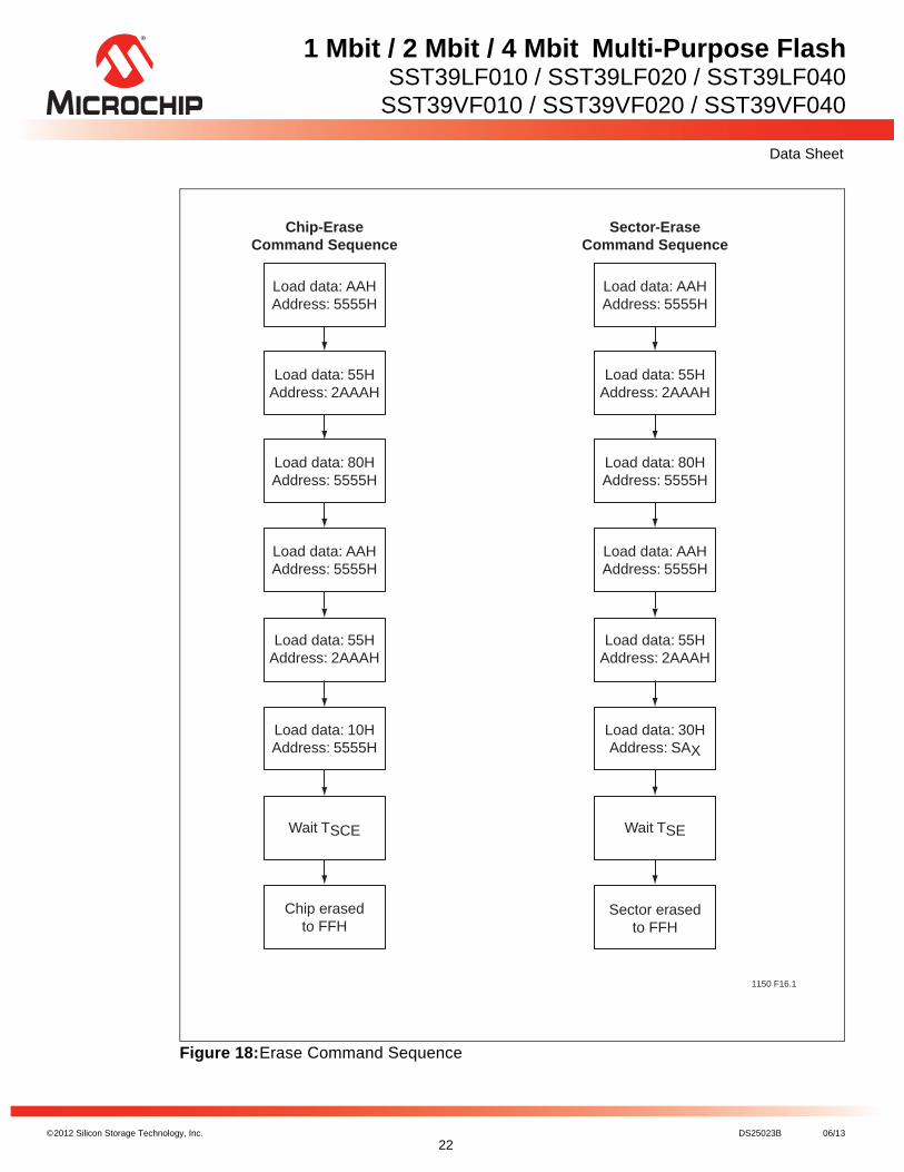
Sector-Erase OperationThe Sector-Erase operation allows the system to erase the device on a sector-by-sector basis. Thesector architecture is based on uniform sector size of 4 KByte. The Sector-Erase operation is initiatedby executing a six-byte command sequence with Sector-Erase command (30H) and sector address(SA) in the last bus cycle. The sector address is latched on the falling edge of the sixth WE# pulse,while the command (30H) is latched on the rising edge of the sixth WE# pulse. The internal Eraseoperation begins after the sixth WE# pulse. The End-of-Erase can be determined using either Data#Polling or Toggle Bit methods. See Figure 9 for timing waveforms. Any commands written during theSector-Erase operation will be ignored.
Chip-Erase OperationThe SST39LF010/020/040 and SST39VF010/020/040 devices provide a Chip-Erase operation, whichallows the user to erase the entire memory array to the ‘1’s state. This is useful when the entire devicemust be quickly erased.
The Chip-Erase operation is initiated by executing a six- byte Software Data Protection commandsequence with Chip-Erase command (10H) with address 5555H in the last byte sequence. The internalErase operation begins with the rising edge of the sixth WE# or CE#, whichever occurs first. During the
©2012 Silicon Storage Technology, Inc. DS25023B 06/13
7
1 Mbit / 2 Mbit / 4 Mbit Multi-Purpose FlashSST39LF010 / SST39LF020 / SST39LF040
SST39VF010 / SST39VF020 / SST39VF040
Data Sheet
internal Erase operation, the only valid read is Toggle Bit or Data# Polling. See Table 4 for the com-mand sequence, Figure 10 for timing diagram, and Figure 18 for the flowchart. Any commands writtenduring the Chip-Erase operation will be ignored.
Write Operation Status DetectionThe SST39LF010/020/040 and SST39VF010/020/040 devices provide two software means to detectthe completion of a Write (Program or Erase) cycle, in order to optimize the system write cycle time.The software detection includes two status bits: Data# Polling (DQ7) and Toggle Bit (DQ6). The End-of-Write detection mode is enabled after the rising edge of WE# which initiates the internal Program orErase operation.
The actual completion of the nonvolatile write is asynchronous with the system; therefore, either aData# Polling or Toggle Bit read may be simultaneous with the completion of the Write cycle. If thisoccurs, the system may possibly get an erroneous result, i.e., valid data may appear to conflict witheither DQ7 or DQ6. In order to prevent spurious rejection, if an erroneous result occurs, the softwareroutine should include a loop to read the accessed location an additional two (2) times. If both readsare valid, then the device has completed the Write cycle, otherwise the rejection is valid.
©2012 Silicon Storage Technology, Inc. DS25023B 06/13
8
1 Mbit / 2 Mbit / 4 Mbit Multi-Purpose FlashSST39LF010 / SST39LF020 / SST39LF040
SST39VF010 / SST39VF020 / SST39VF040
Data Sheet
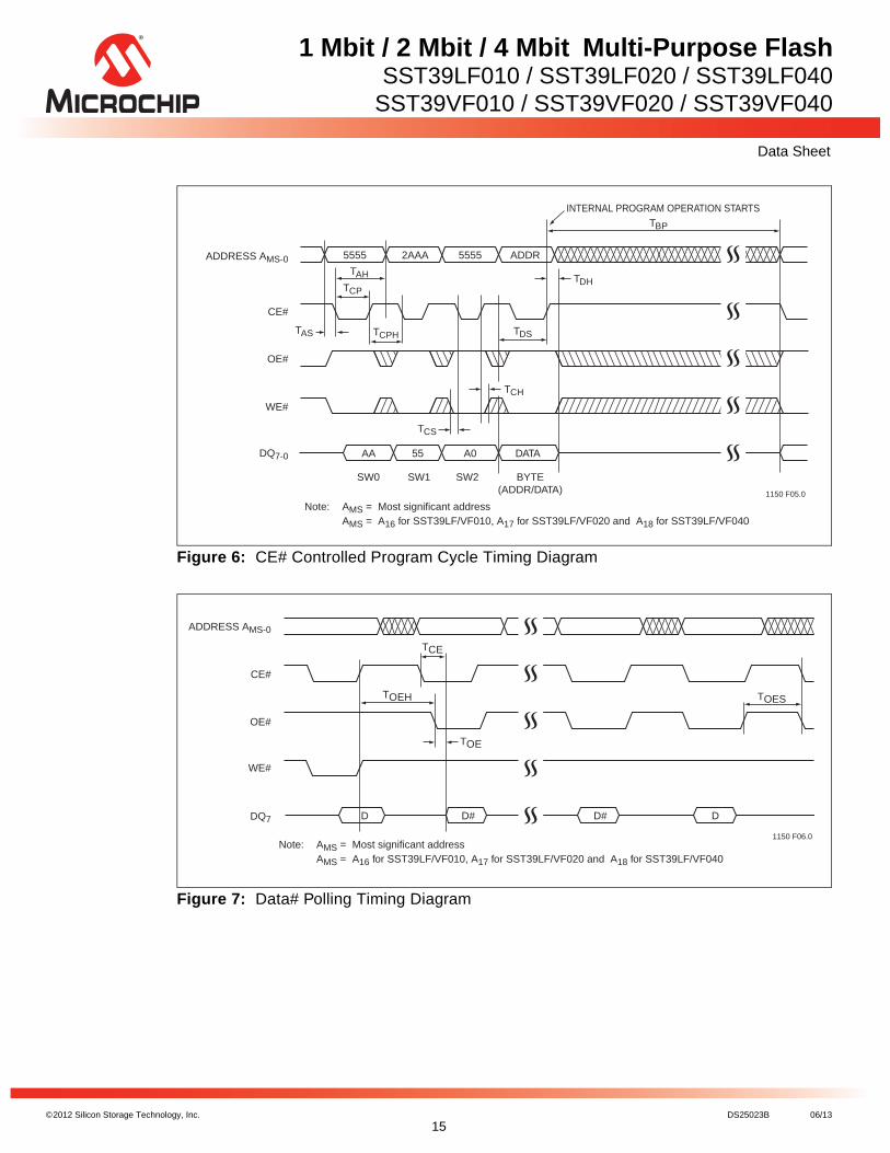
Data# Polling (DQ7)When the SST39LF010/020/040 and SST39VF010/020/040 are in the internal Program operation, anyattempt to read DQ7 will produce the complement of the true data. Once the Program operation iscompleted, DQ7 will produce true data. Note that even though DQ7 may have valid data immediatelyfollowing completion of an internal Write operation, the remaining data outputs may still be invalid: validdata on the entire data bus will appear in subsequent successive Read cycles after an interval of 1 µs.During internal Erase operation, any attempt to read DQ7 will produce a “0”. Once the internal Eraseoperation is completed, DQ7 will produce a “1”. The Data# Polling is valid after the rising edge of fourthWE# (or CE#) pulse for Program operation. For Sector- or Chip-Erase, the Data# Polling is valid afterthe rising edge of sixth WE# (or CE#) pulse. See Figure 7 for Data# Polling timing diagram and Figure16 for a flowchart.
Toggle Bit (DQ6)During the internal Program or Erase operation, any consecutive attempts to read DQ6 will producealternating ‘0’s and ‘1’s, i.e., toggling between 0 and 1. When the internal Program or Erase operationis completed, the toggling will stop. The device is then ready for the next operation. The Toggle Bit isvalid after the rising edge of fourth WE# (or CE#) pulse for Program operation. For Sector- or Chip-Erase, the Toggle Bit is valid after the rising edge of sixth WE# (or CE#) pulse. See Figure 8 for ToggleBit timing diagram and Figure 16 for a flowchart.
Data ProtectionThe SST39LF010/020/040 and SST39VF010/020/040 provide both hardware and software features toprotect nonvolatile data from inadvertent writes.
Hardware Data ProtectionNoise/Glitch Protection: A WE# or CE# pulse of less than 5 ns will not initiate a Write cycle.
VDD Power Up/Down Detection: The Write operation is inhibited when VDD is less than 1.5V.
Write Inhibit Mode: Forcing OE# low, CE# high, or WE# high will inhibit the Write operation. This pre-vents inadvertent writes during power-up or power-down.

©2012 Silicon Storage Technology, Inc. DS25023B 06/13
9
1 Mbit / 2 Mbit / 4 Mbit Multi-Purpose FlashSST39LF010 / SST39LF020 / SST39LF040
SST39VF010 / SST39VF020 / SST39VF040
Data Sheet
Software Data Protection (SDP)The SST39LF010/020/040 and SST39VF010/020/040 provide the JEDEC approved Software DataProtection scheme for all data alteration operation, i.e., Program and Erase. Any Program operationrequires the inclusion of a series of three-byte sequence. The three-byte load sequence is used to ini-tiate the Program operation, providing optimal protection from inadvertent Write operations, e.g., dur-ing the system power-up or power-down. Any Erase operation requires the inclusion of six-byte loadsequence. These devices are shipped with the Software Data Protection permanently enabled. SeeTable 4 for the specific software command codes. During SDP command sequence, invalid commandswill abort the device to read mode, within TRC.
Product IdentificationThe Product Identification mode identifies the devices as the SST39LF/VF010, SST39LF/VF020, andSST39LF/VF040 and manufacturer as SST. This mode may be accessed by software operations.Users may use the Software Product Identification operation to identify the part (i.e., using the deviceID) when using multiple manufacturers in the same socket. For details, see Table 4 for software opera-tion, Figure 11 for the Software ID Entry and Read timing diagram, and Figure 17 for the Software IDentry command sequence flowchart.
Product Identification Mode Exit/ResetIn order to return to the standard Read mode, the Software Product Identification mode must be exited.Exit is accomplished by issuing the Software ID Exit command sequence, which returns the device tothe Read operation. Please note that the Software ID Exit command is ignored during an internal Pro-gram or Erase operation. See Table 4 for software command codes, Figure 12 for timing waveform,and Figure 17 for a flowchart.
Table 2: Product Identification
Address Data
Manufacturer’s ID 0000H BFH
Device ID
SST39LF/VF010 0001H D5H
SST39LF/VF020 0001H D6H
SST39LF/VF040 0001H D7HT2.1 25023
©2012 Silicon Storage Technology, Inc. DS25023B 06/13
10
1 Mbit / 2 Mbit / 4 Mbit Multi-Purpose FlashSST39LF010 / SST39LF020 / SST39LF040
SST39VF010 / SST39VF020 / SST39VF040
Data Sheet
Operations
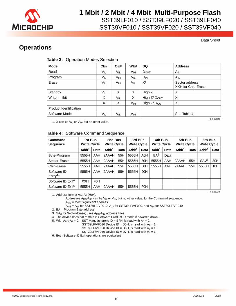
Table 3: Operation Modes Selection
Mode CE# OE# WE# DQ Address
Read VIL VIL VIH DOUT AIN
Program VIL VIH VIL DIN AIN
Erase VIL VIH VIL X1
1. X can be VIL or VIH, but no other value.
Sector address,XXH for Chip-Erase
Standby VIH X X High Z X
Write Inhibit X VIL X High Z/ DOUT X
X X VIH High Z/ DOUT X
Product Identification
Software Mode VIL VIL VIH See Table 4T3.4 25023
Table 4: Software Command Sequence
CommandSequence
1st BusWrite Cycle
2nd BusWrite Cycle
3rd BusWrite Cycle
4th BusWrite Cycle
5th BusWrite Cycle
6th BusWrite Cycle
Addr1
1. Address format A14-A0 (Hex),Addresses AMS-A15 can be VIL or VIH, but no other value, for the Command sequence.AMS = Most significant addressAMS = A16 for SST39LF/VF010, A17 for SST39LF/VF020, and A18 for SST39LF/VF040
Data Addr1 Data Addr1 Data Addr1 Data Addr1 Data Addr1 Data
Byte-Program 5555H AAH 2AAAH 55H 5555H A0H BA2
2. BA = Program Byte address
Data
Sector-Erase 5555H AAH 2AAAH 55H 5555H 80H 5555H AAH 2AAAH 55H SAX3
3. SAX for Sector-Erase; uses AMS-A12 address lines
30H
Chip-Erase 5555H AAH 2AAAH 55H 5555H 80H 5555H AAH 2AAAH 55H 5555H 10H
Software ID Entry4,5
4. The device does not remain in Software Product ID mode if powered down.5. With AMS-A1 = 0; SST Manufacturer’s ID = BFH, is read with A0 = 0,
SST39LF/VF010 Device ID = D5H, is read with A0 = 1,SST39LF/VF020 Device ID = D6H, is read with A0 = 1,SST39LF/VF040 Device ID = D7H, is read with A0 = 1.
5555H AAH 2AAAH 55H 5555H 90H
Software ID Exit6
6. Both Software ID Exit operations are equivalent
XXH F0H
Software ID Exit6 5555H AAH 2AAAH 55H 5555H F0HT4.2 25023
©2012 Silicon Storage Technology, Inc. DS25023B 06/13
11
1 Mbit / 2 Mbit / 4 Mbit Multi-Purpose FlashSST39LF010 / SST39LF020 / SST39LF040
SST39VF010 / SST39VF020 / SST39VF040
Data Sheet
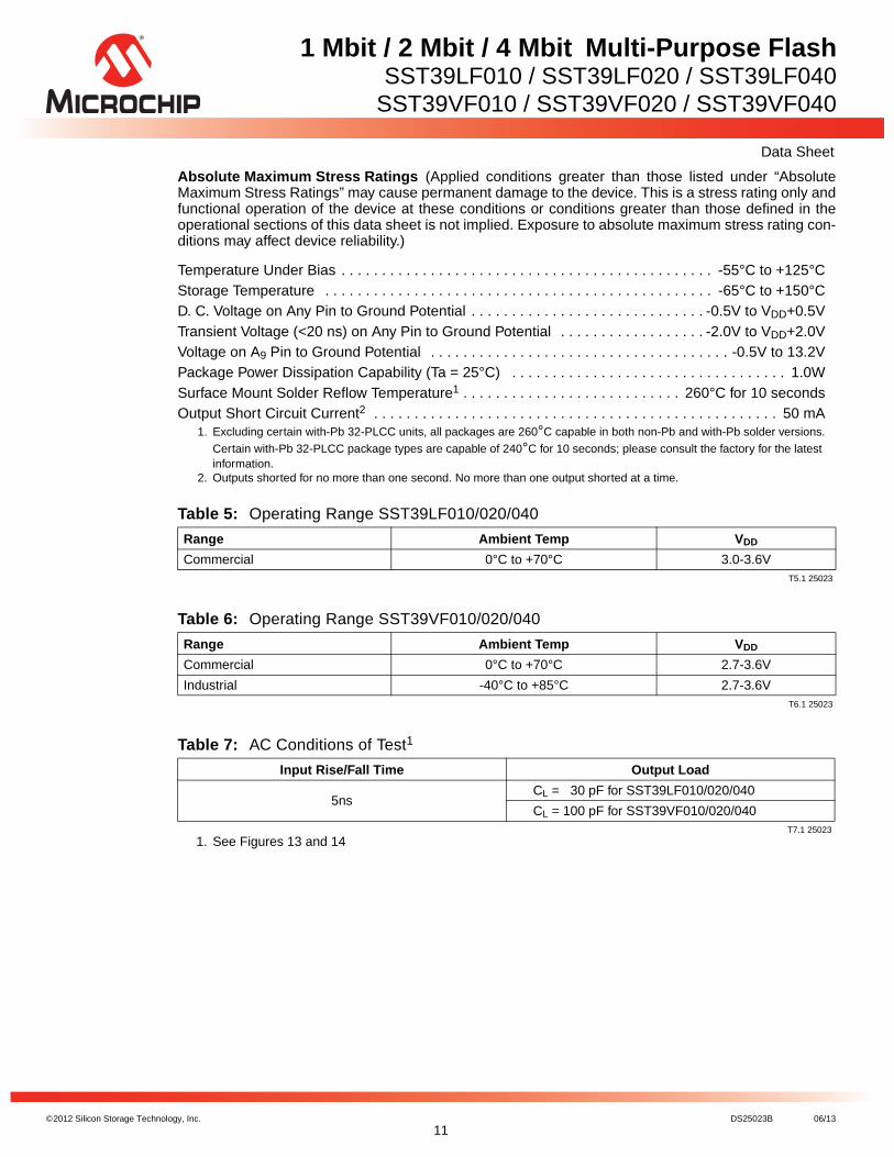
Absolute Maximum Stress Ratings (Applied conditions greater than those listed under “AbsoluteMaximum Stress Ratings” may cause permanent damage to the device. This is a stress rating only andfunctional operation of the device at these conditions or conditions greater than those defined in theoperational sections of this data sheet is not implied. Exposure to absolute maximum stress rating con-ditions may affect device reliability.)
Temperature Under Bias . . . . . . . . . . . . . . . . . . . . . . . . . . . . . . . . . . . . . . . . . . . . . . -55°C to +125°CStorage Temperature . . . . . . . . . . . . . . . . . . . . . . . . . . . . . . . . . . . . . . . . . . . . . . . . -65°C to +150°CD. C. Voltage on Any Pin to Ground Potential . . . . . . . . . . . . . . . . . . . . . . . . . . . . . -0.5V to VDD+0.5VTransient Voltage (<20 ns) on Any Pin to Ground Potential . . . . . . . . . . . . . . . . . . -2.0V to VDD+2.0VVoltage on A9 Pin to Ground Potential . . . . . . . . . . . . . . . . . . . . . . . . . . . . . . . . . . . . . -0.5V to 13.2VPackage Power Dissipation Capability (Ta = 25°C) . . . . . . . . . . . . . . . . . . . . . . . . . . . . . . . . . . 1.0WSurface Mount Solder Reflow Temperature1 . . . . . . . . . . . . . . . . . . . . . . . . . . . 260°C for 10 secondsOutput Short Circuit Current2 . . . . . . . . . . . . . . . . . . . . . . . . . . . . . . . . . . . . . . . . . . . . . . . . . . 50 mA
1. Excluding certain with-Pb 32-PLCC units, all packages are 260°C capable in both non-Pb and with-Pb solder versions.
Certain with-Pb 32-PLCC package types are capable of 240°C for 10 seconds; please consult the factory for the latest information.
2. Outputs shorted for no more than one second. No more than one output shorted at a time.
Table 5: Operating Range SST39LF010/020/040
Range Ambient Temp VDD
Commercial 0°C to +70°C 3.0-3.6VT5.1 25023
Table 6: Operating Range SST39VF010/020/040
Range Ambient Temp VDD
Commercial 0°C to +70°C 2.7-3.6V
Industrial -40°C to +85°C 2.7-3.6VT6.1 25023
Table 7: AC Conditions of Test1
1. See Figures 13 and 14
Input Rise/Fall Time Output Load
5nsCL = 30 pF for SST39LF010/020/040
CL = 100 pF for SST39VF010/020/040T7.1 25023

©2012 Silicon Storage Technology, Inc. DS25023B 06/13
12
1 Mbit / 2 Mbit / 4 Mbit Multi-Purpose FlashSST39LF010 / SST39LF020 / SST39LF040
SST39VF010 / SST39VF020 / SST39VF040
Data Sheet
Table 8: DC Operating Characteristics -VDD = 3.0-3.6V for SST39LF010/020/040 and 2.7-3.6V for SST39VF010/020/0401
Symbol Parameter
Limits
Test ConditionsMin Max Units
IDD Power Supply Current Address input=VILT/VIHT, at f=1/TRC MinVDD=VDD Max
Read2 20 mA CE#=VIL, OE#=WE#=VIH, all I/Os open
Program and Erase3 30 mA CE#=WE#=VIL, OE#=VIH
ISB Standby VDD Current 15 µA CE#=VIHC, VDD=VDD Max
ILI Input Leakage Current 1 µA VIN=GND to VDD, VDD=VDD Max
ILO Output Leakage Current 10 µA VOUT=GND to VDD, VDD=VDD Max
VIL Input Low Voltage 0.8 V VDD=VDD Min
VIH Input High Voltage 0.7VDD V VDD=VDD Max
VIHC Input High Voltage (CMOS) VDD-0.3 V VDD=VDD Max
VOL Output Low Voltage 0.2 V IOL=100 µA, VDD=VDD Min
VOH Output High Voltage VDD-0.2 V IOH=-100 µA, VDD=VDD MinT8.7 25023
1. Typical conditions for the Active Current shown on the front data sheet page are average values at 25°C(room temperature), and VDD = 3V for VF devices. Not 100% tested.
2. Values are for 70 ns conditions. See the Multi-Purpose Flash Power Rating application note for further information.3. 30 mA max for Erase operations in the industrial temperature range.
Table 9: Recommended System Power-up Timings
Symbol Parameter Minimum Units
TPU-READ1
1. This parameter is measured only for initial qualification and after a design or process change that could affect this parameter.
Power-up to Read Operation 100 µs
TPU-WRITE1 Power-up to Program/Erase Operation 100 µs
T9.1 25023
Table 10:Capacitance (Ta = 25°C, f=1 Mhz, other pins open)
Parameter Description Test Condition Maximum
CI/O1
1. This parameter is measured only for initial qualification and after a design or process change that could affect this parameter.
I/O Pin Capacitance VI/O = 0V 12 pF
CIN1 Input Capacitance VIN = 0V 6 pF
T10.0 25023
Table 11:Reliability Characteristics
Symbol Parameter Minimum Specification Units Test Method
NEND1,2
1. This parameter is measured only for initial qualification and after a design or process change that could affect this parameter.
2. NEND endurance rating is qualified as a 10,000 cycle minimum for the whole device. A sector- or block-level rating would result in a higher minimum specification.
Endurance 10,000 Cycles JEDEC Standard A117
TDR1 Data Retention 100 Years JEDEC Standard A103
ILTH1 Latch Up 100 + IDD mA JEDEC Standard 78
T11.3 25023

©2012 Silicon Storage Technology, Inc. DS25023B 06/13
13
1 Mbit / 2 Mbit / 4 Mbit Multi-Purpose FlashSST39LF010 / SST39LF020 / SST39LF040
SST39VF010 / SST39VF020 / SST39VF040
Data Sheet
AC Characteristics
Table 12:Read Cycle Timing Parameters - VDD = 3.0-3.6V for SST39LF010/020/040 and 2.7-3.6V for SST39VF010/020/040
Symbol Parameter
SST39LF010-55SST39LF020-55SST39LF040-55
SST39VF010-70SST39VF020-70SST39VF040-70
UnitsMin Max Min Max
TRC Read Cycle Time 55 70 ns
TCE Chip Enable Access Time 55 70 ns
TAA Address Access Time 55 70 ns
TOE Output Enable Access Time 30 35 ns
TCLZ1
1. This parameter is measured only for initial qualification and after a design or process change that could affect this parameter.
CE# Low to Active Output 0 0 ns
TOLZ1 OE# Low to Active Output 0 0 ns
TCHZ1 CE# High to High-Z Output 15 25 ns
TOHZ1 OE# High to High-Z Output 15 25 ns
TOH1 Output Hold from Address Change 0 0 ns
T12.2 25023
Table 13:Program/Erase Cycle Timing Parameters
Symbol Parameter Min Max Units
TBP Byte-Program Time 20 µs
TAS Address Setup Time 0 ns
TAH Address Hold Time 30 ns
TCS WE# and CE# Setup Time 0 ns
TCH WE# and CE# Hold Time 0 ns
TOES OE# High Setup Time 0 ns
TOEH OE# High Hold Time 10 ns
TCP CE# Pulse Width 40 ns
TWP WE# Pulse Width 40 ns
TWPH1
1. This parameter is measured only for initial qualification and after a design or process change that could affect this parameter.
WE# Pulse Width High 30 ns
TCPH1 CE# Pulse Width High 30 ns
TDS Data Setup Time 40 ns
TDH1 Data Hold Time 0 ns
TIDA1 Software ID Access and Exit Time 150 ns
TSE Sector-Erase 25 ms
TSCE Chip-Erase 100 msT13.1 25023

©2012 Silicon Storage Technology, Inc. DS25023B 06/13
14
1 Mbit / 2 Mbit / 4 Mbit Multi-Purpose FlashSST39LF010 / SST39LF020 / SST39LF040
SST39VF010 / SST39VF020 / SST39VF040
Data Sheet
Figure 4: Read Cycle Timing Diagram
Figure 5: WE# Controlled Program Cycle Timing Diagram
1150 F03.0
ADDRESS AMS-0
DQ7-0
WE#
OE#
CE#
TCE
TRC TAA
TOE
TOLZVIH
HIGH-Z
TCLZ TOH TCHZ
HIGH-ZDATA VALIDDATA VALID
TOHZ
Note: AMS = Most significant address AMS = A16 for SST39LF/VF010, A17 for SST39LF/VF020 and A18 for SST39LF/VF040
1150 F04.0
ADDRESS AMS-0
DQ7-0
TDH
TWPHTDS
TWP
TAH
TAS
TCH
TCS
CE#
SW0 SW1 SW2
5555 2AAA 5555 ADDR
AA 55 A0 DATA
INTERNAL PROGRAM OPERATION STARTS
BYTE(ADDR/DATA)
OE#
WE#
TBP
Note: AMS = Most significant address AMS = A16 for SST39LF/VF010, A17 for SST39LF/VF020 and A18 for SST39LF/VF040
©2012 Silicon Storage Technology, Inc. DS25023B 06/13
15
1 Mbit / 2 Mbit / 4 Mbit Multi-Purpose FlashSST39LF010 / SST39LF020 / SST39LF040
SST39VF010 / SST39VF020 / SST39VF040
Data Sheet
Figure 6: CE# Controlled Program Cycle Timing Diagram
Figure 7: Data# Polling Timing Diagram
1150 F05.0
ADDRESS AMS-0
DQ7-0
TDH
TCPH TDS
TCP
TAH
TAS
TCH
TCS
WE#
SW0 SW1 SW2
5555 2AAA 5555 ADDR
AA 55 A0 DATA
INTERNAL PROGRAM OPERATION STARTS
BYTE(ADDR/DATA)
OE#
CE#
TBP
Note: AMS = Most significant address AMS = A16 for SST39LF/VF010, A17 for SST39LF/VF020 and A18 for SST39LF/VF040
1150 F06.0
ADDRESS AMS-0
DQ7 D D# D# D
WE#
OE#
CE#
TOEH
TOE
TCE
TOES
Note: AMS = Most significant address AMS = A16 for SST39LF/VF010, A17 for SST39LF/VF020 and A18 for SST39LF/VF040

©2012 Silicon Storage Technology, Inc. DS25023B 06/13
16
1 Mbit / 2 Mbit / 4 Mbit Multi-Purpose FlashSST39LF010 / SST39LF020 / SST39LF040
SST39VF010 / SST39VF020 / SST39VF040
Data Sheet
Figure 8: Toggle Bit Timing Diagram
Figure 9: WE# Controlled Sector-Erase Timing Diagram
1150 F07.0
ADDRESS AMS-0
DQ6
WE#
OE#
CE#
TOETOEH
TCE
TOES
TWO READ CYCLESWITH SAME OUTPUTSNote: AMS = Most significant address
AMS = A16 for SST39LF/VF010, A17 for SST39LF/VF020 and A18 for SST39LF/VF040
1150 F08.0
ADDRESS AMS-0
DQ7-0
WE#
SW0 SW1 SW2 SW3 SW4 SW5
5555 2AAA 2AAA5555 5555
55 3055AA 80 AA
SAX
OE#
CE#
SIX-BYTE CODE FOR SECTOR-ERASE TSE
TWP
Note: This device also supports CE# controlled Sector-Erase operation. The WE# and CE# signals are interchageable as long as minmum timings are met. (See Table 10) SAX = Sector Address
AMS = Most significant address AMS = A16 for SST39LF/VF010, A17 for SST39LF/VF020, and A18 for SST39LF/VF040

©2012 Silicon Storage Technology, Inc. DS25023B 06/13
17
1 Mbit / 2 Mbit / 4 Mbit Multi-Purpose FlashSST39LF010 / SST39LF020 / SST39LF040
SST39VF010 / SST39VF020 / SST39VF040
Data Sheet
Figure 10:WE# Controlled Chip-Erase Timing Diagram
Figure 11:Software ID Entry and Read
1150 F17.0
ADDRESS AMS-0
DQ7-0
WE#
SW0 SW1 SW2 SW3 SW4 SW5
5555 2AAA 2AAA5555 5555
55 1055AA 80 AA
5555
OE#
CE#
SIX-BYTE CODE FOR CHIP-ERASE TSCE
TWP
Note: This device also supports CE# controlled Chip-Erase operation. The WE# and CE# signals are interchageable as long as minmum timings are met. (See Table 10)
AMS = Most significant address AMS = A16 for SST39LF/VF010, A17 for SST39LF/VF020, and A18 for SST39LF/VF040
1150 F09.2
Note: Device ID = D5H for SST39LF/VF010, D6H for SST39LF/VF020, and D7H for SST39LF/VF040.
ADDRESS A14-0
TIDA
DQ7-0
WE#
SW0 SW1 SW2
5555 2AAA 5555 0000 0001
OE#
CE#
Three-byte Sequence for Software ID Entry
TWP
TWPH TAA
BF Device ID55AA 90

©2012 Silicon Storage Technology, Inc. DS25023B 06/13
18
1 Mbit / 2 Mbit / 4 Mbit Multi-Purpose FlashSST39LF010 / SST39LF020 / SST39LF040
SST39VF010 / SST39VF020 / SST39VF040
Data Sheet
Figure 12:Software ID Exit and Reset
Figure 13:AC Input/Output Reference Waveforms
Figure 14:A Test Load Example
1150 F10.0
ADDRESS A14-0
DQ7-0
TIDA
TWP
TWHP
WE#
SW0 SW1 SW2
5555 2AAA 5555
THREE-BYTE SEQUENCE FORSOFTWARE ID EXIT AND RESET
OE#
CE#
AA 55 F0
1150 F12.1
REFERENCE POINTS OUTPUTINPUT VIT
VIHT
VILT
VOT
AC test inputs are driven at VIHT (0.9 VDD) for a logic “1” and VILT (0.1 VDD) for a logic“0”. Measurement reference points for inputs and outputs are VIT (0.5 VDD) and VOT (0.5 VDD). Inputrise and fall times (10% ↔ 90%) are <5 ns.
Note: VIT - VINPUT TestVOT - VOUTPUT TestVIHT - VINPUT HIGH TestVILT - VINPUT LOW Test
1150 F11.1
TO TESTER
TO DUT
CL
©2012 Silicon Storage Technology, Inc. DS25023B 06/13
19
1 Mbit / 2 Mbit / 4 Mbit Multi-Purpose FlashSST39LF010 / SST39LF020 / SST39LF040
SST39VF010 / SST39VF020 / SST39VF040
Data Sheet
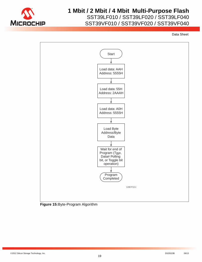
Figure 15:Byte-Program Algorithm
1150 F13.1
Start
Load data: AAHAddress: 5555H
Load data: 55HAddress: 2AAAH
Load data: A0HAddress: 5555H
Load ByteAddress/Byte
Data
Wait for end ofProgram (TBP, Data# Polling
bit, or Toggle bitoperation)
ProgramCompleted

©2012 Silicon Storage Technology, Inc. DS25023B 06/13
20
1 Mbit / 2 Mbit / 4 Mbit Multi-Purpose FlashSST39LF010 / SST39LF020 / SST39LF040
SST39VF010 / SST39VF020 / SST39VF040
Data Sheet
Figure 16:Wait Options
1150 F14.0
Wait TBP,TSCE, or TSE
Byte-Program/Erase
Initiated
Internal Timer Toggle Bit
Yes
Yes
No
No
Program/EraseCompleted
Does DQ6match?
Read samebyte
Data# Polling
Program/EraseCompleted
Program/EraseCompleted
Read byte
Is DQ7 =true data?
Read DQ7
Byte-Program/Erase
Initiated
Byte-Program/Erase
Initiated

©2012 Silicon Storage Technology, Inc. DS25023B 06/13
21
1 Mbit / 2 Mbit / 4 Mbit Multi-Purpose FlashSST39LF010 / SST39LF020 / SST39LF040
SST39VF010 / SST39VF020 / SST39VF040
Data Sheet
Figure 17:Software ID Command Flowcharts
1150 F15.2
Load data: AAHAddress: 5555H
Software ID EntryCommand Sequence
Load data: 55HAddress: 2AAAH
Load data: 90HAddress: 5555H
Wait TIDA
Read Software ID
Load data: AAHAddress: 5555H
Software ID Exit &Reset Command Sequence
Load data: 55HAddress: 2AAAH
Load data: F0HAddress: 5555H
Load data: F0HAddress: XXH
Return to normaloperation
Wait TIDA
Wait TIDA
Return to normaloperation
©2012 Silicon Storage Technology, Inc. DS25023B 06/13
22
1 Mbit / 2 Mbit / 4 Mbit Multi-Purpose FlashSST39LF010 / SST39LF020 / SST39LF040
SST39VF010 / SST39VF020 / SST39VF040
Data Sheet
Figure 18:Erase Command Sequence
1150 F16.1
Load data: AAHAddress: 5555H
Chip-EraseCommand Sequence
Load data: 55HAddress: 2AAAH
Load data: 80HAddress: 5555H
Load data: 55HAddress: 2AAAH
Load data: 10HAddress: 5555H
Load data: AAHAddress: 5555H
Wait TSCE
Chip erasedto FFH
Load data: AAHAddress: 5555H
Sector-EraseCommand Sequence
Load data: 55HAddress: 2AAAH
Load data: 80HAddress: 5555H
Load data: 55HAddress: 2AAAH
Load data: 30HAddress: SAX
Load data: AAHAddress: 5555H
Wait TSE
Sector erasedto FFH

©2012 Silicon Storage Technology, Inc. DS25023B 06/13
23
1 Mbit / 2 Mbit / 4 Mbit Multi-Purpose FlashSST39LF010 / SST39LF020 / SST39LF040
SST39VF010 / SST39VF020 / SST39VF040
Data Sheet
Product Ordering Information
SST 39 VF 010 - 55 - 4C - NHE
XX XX XXX - XX - XX - XXX
Environmental AttributeE1 = non-Pb
Package ModifierH = 32 leads
Package TypeN = PLCCW = TSOP (type 1, die up, 8mm x 14mm)
Temperature RangeC = Commercial = 0°C to +70°CI = Industrial = -40°C to +85°C
Minimum Endurance4 = 10,000 cycles
Read Access Speed55 = 55 ns70 = 70 ns
Device Density040 = 4 Mbit020 = 2 Mbit010 = 1 Mbit
VoltageL = 3.0-3.6VV = 2.7-3.6V
Product Series39 = Multi-Purpose Flash
1. Environmental suffix “E” denotes non-Pb solder. SST non-Pb solder devices are RoHS compliant.

©2012 Silicon Storage Technology, Inc. DS25023B 06/13
24
1 Mbit / 2 Mbit / 4 Mbit Multi-Purpose FlashSST39LF010 / SST39LF020 / SST39LF040
SST39VF010 / SST39VF020 / SST39VF040
Data Sheet
Valid combinations for SST39LF010SST39LF010-55-4C-NHE SST39LF010-55-4C-WHE
Valid combinations for SST39VF010SST39VF010-70-4C-NHE SST39VF010-70-4C-WHE
SST39VF010-70-4I-NHE SST39VF010-70-4I-WHE
Valid combinations for SST39LF020SST39LF020-55-4C-NHE SST39LF020-55-4C-WHE
Valid combinations for SST39VF020SST39VF020-70-4C-NHE SST39VF020-70-4C-WHE
SST39VF020-70-4I-NHE SST39VF020-70-4I-WHE
Valid combinations for SST39LF040SST39LF040-55-4C-NHE SST39LF040-55-4C-WHE
Valid combinations for SST39VF040SST39VF040-70-4C-NHE SST39VF040-70-4C-WHE
SST39VF040-70-4I-NHE SST39VF040-70-4I-WHE
Note:Valid combinations are those products in mass production or will be in mass production. Consult your SST sales representative to confirm availability of valid combinations and to determine availability of new combi-nations.

©2012 Silicon Storage Technology, Inc. DS25023B 06/13
25
1 Mbit / 2 Mbit / 4 Mbit Multi-Purpose FlashSST39LF010 / SST39LF020 / SST39LF040
SST39VF010 / SST39VF020 / SST39VF040
Data Sheet
Packaging Diagrams
Figure 19:32-lead Plastic Lead Chip Carrier (PLCC)SST Package Code: NH
.040
.030
.021
.013.530.490
.095
.075
.140
.125
.032
.026
.032
.026
.029
.023
.453
.447
.553
.547.595.585
.495
.485 .112.106
.042
.048
.048
.042
.015 Min.
TOP VIEW SIDE VIEW BOTTOM VIEW
12 32
.400BSC
32-plcc-NH-3
Note: 1. Complies with JEDEC publication 95 MS-016 AE dimensions, although some dimensions may be more stringent. 2. All linear dimensions are in inches (max/min). 3. Dimensions do not include mold flash. Maximum allowable mold flash is .008 inches. 4. Coplanarity: 4 mils.
.050BSC
.050BSC
OptionalPin #1
Identifier .020 R.MAX.
R.x 30°

©2012 Silicon Storage Technology, Inc. DS25023B 06/13
26
1 Mbit / 2 Mbit / 4 Mbit Multi-Purpose FlashSST39LF010 / SST39LF020 / SST39LF040
SST39VF010 / SST39VF020 / SST39VF040
Data Sheet
Figure 20:32-lead Thin Small Outline Package (TSOP) 8mm x 14mmSST Package Code: WH
32-tsop-WH-7
Note: 1. Complies with JEDEC publication 95 MO-142 BA dimensions, although some dimensions may be more stringent. 2. All linear dimensions are in millimeters (max/min). 3. Coplanarity: 0.1 mm 4. Maximum allowable mold flash is 0.15 mm at the package ends, and 0.25 mm between leads.
1.20max.
1mm
Pin # 1 Identifier
12.5012.30
14.2013.80
0.700.50
8.107.90
0.270.17
0.50BSC
1.050.95
0.150.05
0.700.50
0°- 5°
DETAIL
©2012 Silicon Storage Technology, Inc. DS25023B 06/13
27
1 Mbit / 2 Mbit / 4 Mbit Multi-Purpose FlashSST39LF010 / SST39LF020 / SST39LF040
SST39VF010 / SST39VF020 / SST39VF040
Data Sheet
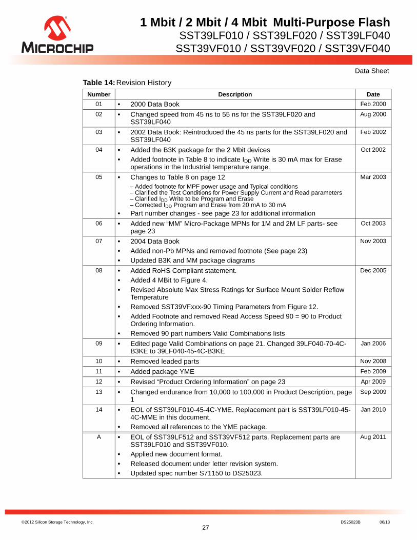
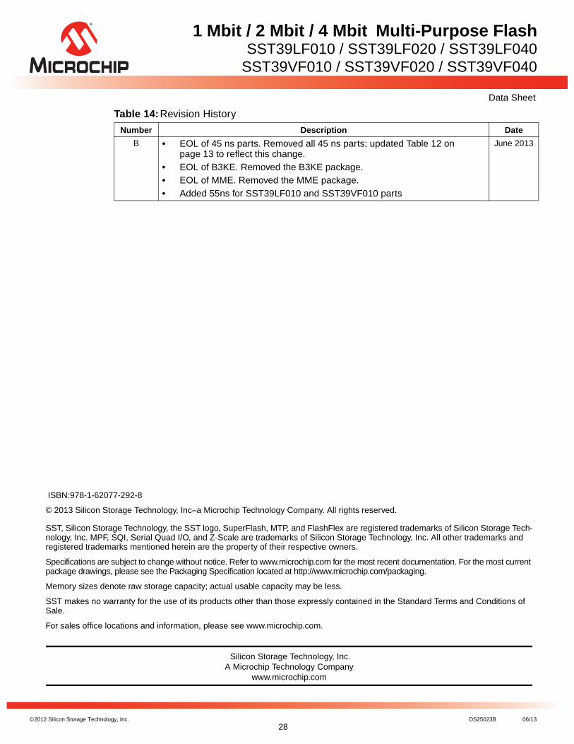
Table 14:Revision History
Number Description Date
01 • 2000 Data Book Feb 2000
02 • Changed speed from 45 ns to 55 ns for the SST39LF020 and SST39LF040
Aug 2000
03 • 2002 Data Book: Reintroduced the 45 ns parts for the SST39LF020 and SST39LF040
Feb 2002
04 • Added the B3K package for the 2 Mbit devices• Added footnote in Table 8 to indicate IDD Write is 30 mA max for Erase
operations in the Industrial temperature range.
Oct 2002
05 • Changes to Table 8 on page 12– Added footnote for MPF power usage and Typical conditions– Clarified the Test Conditions for Power Supply Current and Read parameters– Clarified IDD Write to be Program and Erase– Corrected IDD Program and Erase from 20 mA to 30 mA
• Part number changes - see page 23 for additional information
Mar 2003
06 • Added new “MM” Micro-Package MPNs for 1M and 2M LF parts- see page 23
Oct 2003
07 • 2004 Data Book• Added non-Pb MPNs and removed footnote (See page 23)• Updated B3K and MM package diagrams
Nov 2003
08 • Added RoHS Compliant statement.• Added 4 MBit to Figure 4.• Revised Absolute Max Stress Ratings for Surface Mount Solder Reflow
Temperature • Removed SST39VFxxx-90 Timing Parameters from Figure 12.• Added Footnote and removed Read Access Speed 90 = 90 to Product
Ordering Information.• Removed 90 part numbers Valid Combinations lists
Dec 2005
09 • Edited page Valid Combinations on page 21. Changed 39LF040-70-4C-B3KE to 39LF040-45-4C-B3KE
Jan 2006
10 • Removed leaded parts Nov 2008
11 • Added package YME Feb 2009
12 • Revised “Product Ordering Information” on page 23 Apr 2009
13 • Changed endurance from 10,000 to 100,000 in Product Description, page 1
Sep 2009
14 • EOL of SST39LF010-45-4C-YME. Replacement part is SST39LF010-45-4C-MME in this document.
• Removed all references to the YME package.
Jan 2010
A • EOL of SST39LF512 and SST39VF512 parts. Replacement parts are SST39LF010 and SST39VF010.
• Applied new document format.• Released document under letter revision system.• Updated spec number S71150 to DS25023.
Aug 2011
©2012 Silicon Storage Technology, Inc. DS25023B 06/13
28
1 Mbit / 2 Mbit / 4 Mbit Multi-Purpose FlashSST39LF010 / SST39LF020 / SST39LF040
SST39VF010 / SST39VF020 / SST39VF040
Data Sheet
B • EOL of 45 ns parts. Removed all 45 ns parts; updated Table 12 on page 13 to reflect this change.
• EOL of B3KE. Removed the B3KE package. • EOL of MME. Removed the MME package.• Added 55ns for SST39LF010 and SST39VF010 parts
June 2013
Table 14:Revision History
Number Description Date
© 2013 Silicon Storage Technology, Inc–a Microchip Technology Company. All rights reserved.
SST, Silicon Storage Technology, the SST logo, SuperFlash, MTP, and FlashFlex are registered trademarks of Silicon Storage Tech-nology, Inc. MPF, SQI, Serial Quad I/O, and Z-Scale are trademarks of Silicon Storage Technology, Inc. All other trademarks and registered trademarks mentioned herein are the property of their respective owners.
Specifications are subject to change without notice. Refer to www.microchip.com for the most recent documentation. For the most current package drawings, please see the Packaging Specification located at http://www.microchip.com/packaging.
Memory sizes denote raw storage capacity; actual usable capacity may be less.
SST makes no warranty for the use of its products other than those expressly contained in the Standard Terms and Conditions of Sale.
For sales office locations and information, please see www.microchip.com.
Silicon Storage Technology, Inc.A Microchip Technology Company
www.microchip.com
ISBN:978-1-62077-292-8


