1 LWG2 Power Sequence Introduce Prepared By: Withy He.
20
1 LWG2 Power Sequence Introduce Prepared By: Withy He
-
Upload
melody-tabb -
Category
Documents
-
view
238 -
download
14
Transcript of 1 LWG2 Power Sequence Introduce Prepared By: Withy He.
1
LWG2 Power Sequence Introduce
Prepared By: Withy He

2

3
DC-DC Source
KBC
ICH7-M
DCBATOUT
5V_AUX_S5U4U5
5V_S53D3V_S5
U45
POK
U52U51
1D8V_S3U44
U74 DDR_VREF_S3
DDR_VREF_S0
U27
5V_S03D3V_S01D8V_S0
U6 2D5V_S0
U22
U25 VCC_CORE_S0CPUCORE_ON
1D5V_S0
3D3V_AUX_S5EN1_5
EN2_3D3
S5_EN
S5
S3
S0
PM_SLP_S5#
PM_SLP_S3#
AD+
MOSBT+
MOS
U74
U44 1D05V_S0
POK
POK
EC_PWRBTN#
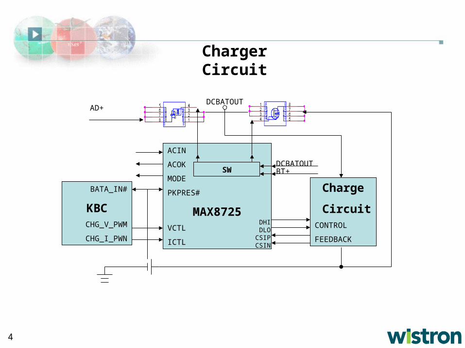
4
Charge
CircuitCONTROL
FEEDBACK
ACIN
ACOK
MODE
PKPRES#
MAX8725VCTL
ICTL
SW
BATA_IN#
KBCCHG_V_PWM
CHG_I_PWN
DCBATOUTBT+
DCBATOUT
DHIDLOCSIPCSIN
AD+
Charger Circuit

5
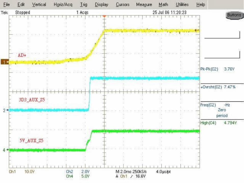
1.Adapter In:
2.Power On:
KBCRE144B
EC_PWRBTN#
S5_EN 5V_S5TPS51120
3D3V_S5
RSMRST#_TO_KBC
PWRBTN#_ICH
SB_RSMRST#
ICH
Adapter In AD+ DCBATOUT 3D3V_AUX_S55V_AUX_S5LP2951 G913MOS MOS
KBC
RE144BRTC_AUX_S5BT+ MOS ICH
H8_RESET#
Power On/Reset Step

6
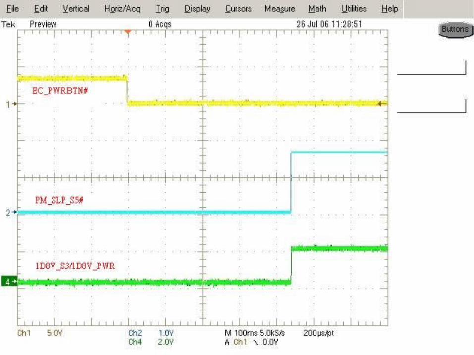
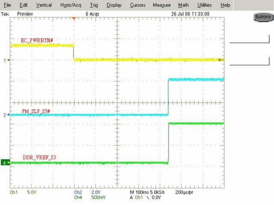
4.S0:
ICH
PM_SLP_S5#TPS51124
TPS51100
1D8V_S3
DDR_VREF_S3
3.S3:
ICH
TPS51100PM_SLP_S3#
MOS
MOS 3D3V_S0
5V_S0
MOS
APL5912_KAC
1D8V_S0
1D5V_S0
APL5332KAC 2D5V_S0
DDR_VREF_S0
TPS51124 1D05V_S0

7
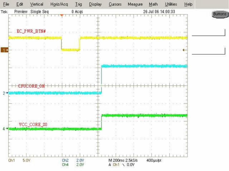
5.VCC_CORE_S0:
TPS51120
POK
APL5912_KAC
POK
TPS51124 POK
CPUCORE_ON ISL6262 VCC_CORE_S0
6.System Reset:
CLK_EN#
ISL6262PGOOD VGATE_PWRGD
CPUPWRGD
VRMPWRGD
ICHPWROK PLTRST1#
PCIRST#
RESET#
G792
HCPURST#
MCH CalistogaPWROK RSTIN#
PLT_RST1#
PCIRST1#
GPUDEBUG G.F.
LAN
HDD/CDROMKBC
TI PCI 7412Power SW
H_PWRGD
RESET#
CPUYonah
PWRGOOD
H_CPURST#CLK GENVTT_PWRGD#
PWROK

8
RTC_AUX_S5
AD_IN/AD+
DCBATOUT
5V_AUX_S5/3.3V_AUX_S5
H8_RESET#
EC_PWRBTN#
S5_EN
3D3V_S5/5V_S5
RSMRST#_TO_KBC
PM_RSMRST#
PM_SLP_S4#
1D8V_S3
DDR_VREF_S3
PM_SLP_S3#
5V_S0,D3V_S0,2D5V_S0,
DDR_VREF_S0
1D8V_S0,1D5V_S0,1D05V_S0
CPUCORE_ON
VCC_CORE_S0
VGATE_PWRGD
CLK_EN#
H_PWRGD
PLT_RST#
PCI_RST#
H_CPURST#
Power On/Reset Sequence
9

10

11

12
13
14

15

16

17

18

19
20