Encoder (VHDL and Verilog) Xilinx Implementation and Simulation
Upload
pamela-berryCategory
view
241download
1
1
Introduction to Xilinx ISL8.1i
Schematic Capture and VHDL
1

2
What Every Student Must Do In Room B2421. Start/All Programs2. Locate Modelsim / license Wizard(Click)3. Follower directions4. Repeat steps again5. Your work will be on this computer. You will 6. Use this computer only for Xilinx assignments.7. If the window does not come up use: C:\Modeltech_xe_starter\win32xoem\license.datNote:
Use your regular sign in Laboratories with Xilinx ISL8.1i
2

3
Schematic Capture

4
New Project1. Start Xilinx ISE 8.1i project navigator by double clicking the
ISE icon on your desktop.2. Click on File and select New project
4

5
Project window3. Name your project and project location, then click next
5

6
New Project Wizard4. The Spartan Starter Kit PCB board uses a Xilinx Spartan3 XCS200
FPGA chip which is packaged in a flat thin 256-pin (FT256) ball Grid Array. Set these values the new project Wizard window,
6

7
Create New Source 5. We will add our sources to this project later, so here we skip the
following two steps (create source and add source). Click on Next.
7

8
Project Summary
6. Check the project summary and click Finish
8
9
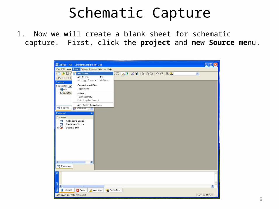
Schematic Capture1. Now we will create a blank sheet for schematic capture.
First, click the project and new Source menu.
9

10
Schematic Capture
10
2. Click Schematic and type in the name for your schematic. Select add to project before clicking Next.

11
Schematic Capture3. Check over the summary and click on Finish
11

12
Schematic Capture
12
4. Check over the Design Summary
13
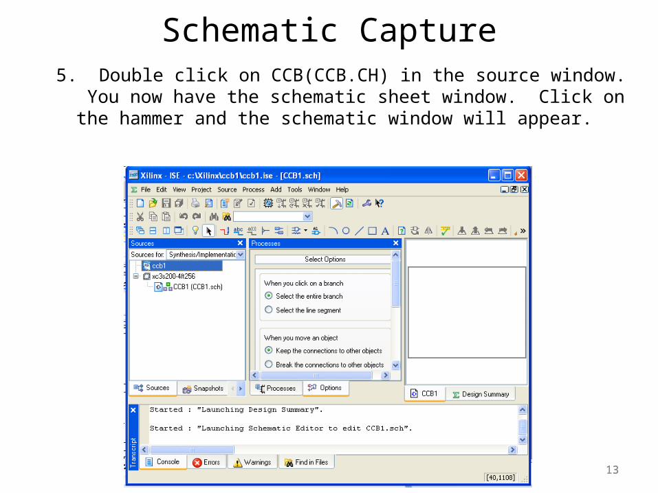
Schematic Capture5. Double click on CCB(CCB.CH) in the source window. You now
have the schematic sheet window. Click on the hammer and the schematic window will appear.
13

14
Schematic Capture
6. Click on the Hammer again

15
Schematic Capture7. Select View and click on Processes
15

16
Schematic Capture8. Click on Add Symbol and locate
a two input and gate (and2)

17
Schematic Capture9. Drag the and2 gate onto the schematic sheet.
Press ESC after each item.

18
Schematic Capture10. Repeat until you have two and2, one or2 and one inv
components on the schematic sheet

19
Schematic Capture12. Click on the wiring tool and wire the schematic as shown.

20
Schematic Capture13. Select the Add I/O Marker and connect the I/O markers
as shown

21
Schematic Capture
14. Double click on each input and output and name them.

22
Schematic Capture15. Schematic with names as shown. F8 zooms the circuit
in and F7 zooms the circuit out.

23
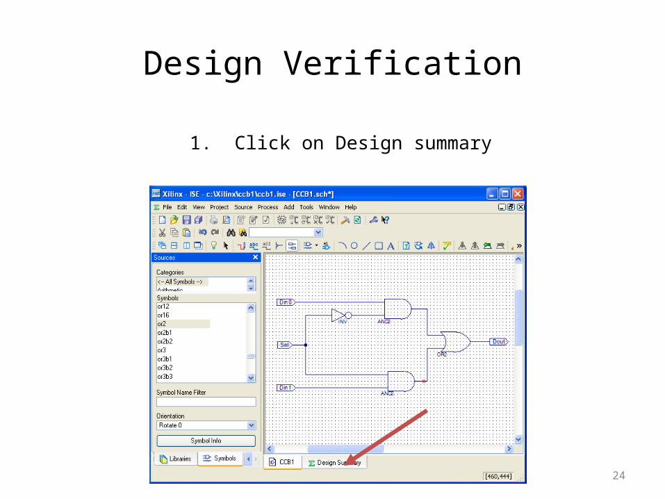
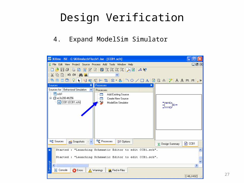
Design Verification
24
Design Verification
1. Click on Design summary

25
Design Verification
2. Select Behavioral Simulation and double click on CCB1.sch

26
Design Verification
3. Click on Processes
27
Design Verification
4. Expand ModelSim Simulator

28
Design Verification
5. Double click on Simulate Behavioral Model

29
Design Verification6. This is the window that appears

30
Design Verification7. At VSIM2> type in force signal-name state-value time as
shown. Enter after run will run the simulation.

31
Synthesize the Design

32
Synthesize the Design1. Click on Xilinx-ISE to get Design Summary and select as shown by
the arrows

33
Synthesize the Design2. Click as shown by the arrow and right click and click on run. A
design is produced.

34
Synthesize the Design
3. Select Project/New Source

35
Synthesize the Design4. Click as shown, type in the File name and click on
Next.

36
Synthesize the Design
5. This window appears, click on Next.

37
Synthesize the Design6. This window appears, click on Finish

38
Synthesize the Design7. The design summary appears, click as shown by the arrow

39
Synthesize the Design
8.

40
Synthesize the Design
9.After saving the pin arrangement, click on OK

41
Synthesize the Design10. After the constraints file has been completed, right click on
Implement Design and select Run.

42
Synthesize the Design
11. Right click on Generate Programming file and select Run

43
Synthesize the Design12. Finally, an FPGA configuration data (*.bit) file is generated.

44
Download and Verify The Design
This is the last step in the design verification process. This section provides instructions for downloading the MUX design onto the Spartan 3 PCB.
1) Connect the 5V DC power cable to the power input on the demo board (J4). (note: you may see a sequence of numbers begin to flash on the 7-segment LEDs, this is just a test configuration stored in the flash memory on the PCB and you can manipulate the various switches and button, except for the PROG button, on the PCB to see the operation of the LEDs and 7-segment displays).
2) Connect the download cable between the PC parallel port and the demo board (J7). 3) Select Synthesis/Implementation from the drop-down list in the Sources window and select Mux_Schematic or Mux_vhdl (or whatever you named you design) in the Sources Window. In the Processes window, expand the Generate Programming File process and double-click the Configure Device (iMPACT) process.

45
Download and Verify The Design1. Processes window, expand the Generate Programming File
process and double-click the Configure Device (iMPACT) process.

46
Download and Verify The Design2. iMPACT opens and the Configure Devices dialog box is displayed. In the
Welcome dialog box, select Configure devices using Boundary-Scan (JTAG). Verify that Automatically connect to a cable and identify Boundary-Scan chain is selected. Click Finish.

47
Download and Verify The Design3. When programming is complete, the Program
Succeeded message is displayed.

48
Download and Verify The Design
4. Close iMPACT without saving. Your design is downloaded into the FPGA and you can begin to verify the design by manipulating swithes/buttons and observing LEDs as specified in your design.