1 General Properties of ZnO
76
1 General Properties of ZnO In this chapter, crystal structure of ZnO encompassing lattice parameters, electronic band structure, mechanical properties, including elastic constants and piezoelectric constants, lattice dynamics, and vibrational processes, thermal properties, electrical properties, and low-field and high-field carrier transport is treated. 1.1 Crystal Structure Most of the group II–VI binary compound semiconductors crystallize in either cubic zinc blende or hexagonal wurtzite (Wz) structure where each anion is surrounded by four cations at the corners of a tetrahedron, and vice versa. This tetrahedral coordination is typical of sp 3 covalent bonding nature, but these materials also have a substantial ionic character that tends to increase the bandgap beyond the one expected from the covalent bonding. ZnO is a II–VI compound semiconductor whose ionicity resides at the borderline between the covalent and ionic semicon- ductors. The crystal structures shared by ZnO are wurtzite (B4), zinc blende 1) (B3), and rocksalt (or Rochelle salt) 2) (B1) as schematically shown in Figure 1.1. B1, B3, and B4 denote the Strukturbericht 3) designations for the three phases. Under ambient conditions, the thermodynamically stable phase is that of wurtzite symmetry. The zinc blende ZnO structure can be stabilized only by growth on cubic substrates, and 1) The term zinc blende originated from com- pounds such as ZnS, which could be in cubic or hexagonal phase. But the term has been used ubiquitously for compound semiconductors with cubic symmetry. The correct term that should be used for the cubic phase of ZnO GaN is actually sphalerite. To be consistent with the diction throughout the literature even at the expense of bordering inaccuracy, the term zinc blende is used throughout this book. 2) Also called Seignette salt – named after Pier Seignette from La Rochelle, France, who first prepared potassium sodium tartrate tetrahy- drate (KNaC 4 H 4 O 6 4= 2 ?) in 1675 and deter- mined its structure. 3) Strukturbericht, the original crystallographic reports. From 1919 to 1939 (Vols 1–8), they were published in Germany. Since then, they have been published in the United States under the name Structure Reports, Acta Crystallographica Section E, by the International Union of Crystallography. j1 Zinc Oxide: Fundamentals, Materials and Device Technology. Hadis Morkoç and Ümit Özg€ ur Copyright Ó 2009 WILEY-VCH Verlag GmbH & Co. KGaA, Weinheim ISBN: 978-3-527-40813-9
-
Upload
doankhuong -
Category
Documents
-
view
236 -
download
5
Transcript of 1 General Properties of ZnO

1General Properties of ZnO
In this chapter, crystal structure of ZnO encompassing lattice parameters, electronicband structure, mechanical properties, including elastic constants and piezoelectricconstants, lattice dynamics, and vibrational processes, thermal properties, electricalproperties, and low-field and high-field carrier transport is treated.
1.1Crystal Structure
Most of the group II–VI binary compound semiconductors crystallize in either cubiczinc blende or hexagonal wurtzite (Wz) structure where each anion is surrounded byfour cations at the corners of a tetrahedron, and vice versa. This tetrahedralcoordination is typical of sp3 covalent bonding nature, but these materials also havea substantial ionic character that tends to increase the bandgap beyond the oneexpected from the covalent bonding. ZnO is a II–VI compound semiconductorwhose ionicity resides at the borderline between the covalent and ionic semicon-ductors. The crystal structures shared byZnO arewurtzite (B4), zinc blende1) (B3), androcksalt (or Rochelle salt)2) (B1) as schematically shown in Figure 1.1. B1, B3, and B4denote the Strukturbericht3) designations for the three phases. Under ambientconditions, the thermodynamically stable phase is that of wurtzite symmetry. Thezinc blende ZnO structure can be stabilized only by growth on cubic substrates, and
1) The term zinc blende originated from com-pounds such as ZnS, which could be in cubic orhexagonal phase. But the term has been usedubiquitously for compound semiconductorswith cubic symmetry. The correct term thatshould be used for the cubic phase of ZnO GaNis actually sphalerite. To be consistent with thediction throughout the literature even at theexpense of bordering inaccuracy, the term zincblende is used throughout this book.
2) Also called Seignette salt – named after PierSeignette from La Rochelle, France, who first
prepared potassium sodium tartrate tetrahy-drate (KNaC4H4O6�4=2?) in 1675 and deter-mined its structure.
3) Strukturbericht, the original crystallographicreports. From 1919 to 1939 (Vols 1–8), they werepublished in Germany. Since then, they havebeen published in the United States under thename Structure Reports, Acta CrystallographicaSection E, by the International Union ofCrystallography.
j1
Zinc Oxide: Fundamentals, Materials and Device Technology. Hadis Morkoç and Ümit Özg€urCopyright � 2009 WILEY-VCH Verlag GmbH & Co. KGaA, WeinheimISBN: 978-3-527-40813-9

the rocksalt or Rochelle salt (NaCl) structure may be obtained at relatively highpressures, as in the case of GaN.The wurtzite structure has a hexagonal unit cell with two lattice parameters a and c
in the ratio of c=a ¼ ffiffiffiffiffiffiffiffi8=3
p ¼ 1:633 (in an ideal wurtzite structure) and belongs to thespace group C4
6v in the Schoenflies notation and P63mc in the Hermann–Mauguinnotation. A schematic representation of the wurtzitic ZnO structure is shown inFigure 1.2. The structure is composed of two interpenetrating hexagonal close-packed (hcp) sublattices, each of which consists of one type of atom displaced withrespect to each other along the threefold c-axis by the amount ofu¼ 3/8¼ 0.375 (in anidealwurtzite structure) in fractional coordinates. The internal parameteru is definedas the length of the bond parallel to the c-axis (anion–cation bond length or the
Figure 1.1 Stick-and-ball representationof ZnOcrystal structures:(a) cubic rocksalt (B1), (b) cubic zinc blende (B3), and(c) hexagonal wurtzite (B4). Shaded gray and black spheresdenote Zn and O atoms, respectively.
Figure 1.2 Schematic representation of a wurtzitic ZnO structurewith lattice constants a in the basal plane and c in the basaldirection, u parameter, which is expressed as the bond length orthe nearest-neighbor distance b divided by c (0.375 in idealcrystal), a and b (109.47� in ideal crystal) bond angles, and threetypes of second-nearest-neighbor distances b01, b02, and b03.
2j 1 General Properties of ZnO
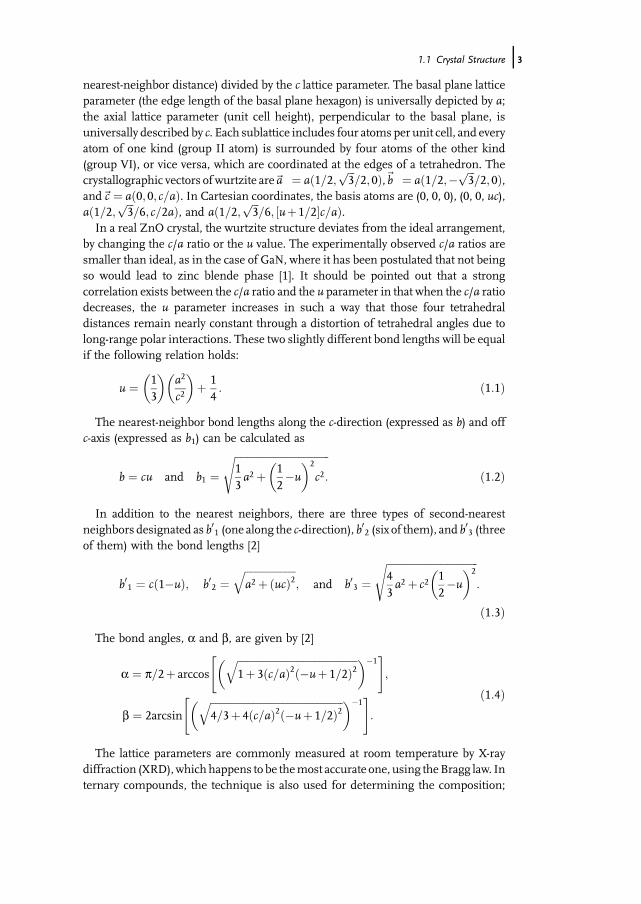
nearest-neighbor distance) divided by the c lattice parameter. The basal plane latticeparameter (the edge length of the basal plane hexagon) is universally depicted by a;the axial lattice parameter (unit cell height), perpendicular to the basal plane, isuniversally described by c. Each sublattice includes four atoms per unit cell, and everyatom of one kind (group II atom) is surrounded by four atoms of the other kind(group VI), or vice versa, which are coordinated at the edges of a tetrahedron. Thecrystallographic vectors ofwurtzite are~a ¼ að1=2; ffiffiffi
3p
=2;0Þ,~b ¼ að1=2;� ffiffiffi3
p=2;0Þ,
and~c ¼ að0;0; c=aÞ. In Cartesian coordinates, the basis atoms are (0, 0, 0), (0, 0, uc),að1=2; ffiffiffi
3p
=6; c=2aÞ, and að1=2; ffiffiffi3
p=6; ½uþ1=2�c=aÞ.
In a real ZnO crystal, the wurtzite structure deviates from the ideal arrangement,by changing the c/a ratio or the u value. The experimentally observed c/a ratios aresmaller than ideal, as in the case of GaN, where it has been postulated that not beingso would lead to zinc blende phase [1]. It should be pointed out that a strongcorrelation exists between the c/a ratio and the u parameter in that when the c/a ratiodecreases, the u parameter increases in such a way that those four tetrahedraldistances remain nearly constant through a distortion of tetrahedral angles due tolong-range polar interactions. These two slightly different bond lengths will be equalif the following relation holds:
u ¼ 13
� �a2
c2
� �þ 1
4: ð1:1Þ
The nearest-neighbor bond lengths along the c-direction (expressed as b) and offc-axis (expressed as b1) can be calculated as
b ¼ cu and b1 ¼ffiffiffiffiffiffiffiffiffiffiffiffiffiffiffiffiffiffiffiffiffiffiffiffiffiffiffiffiffiffiffiffiffiffiffiffiffi13a2 þ 1
2�u
� �2
c2:
sð1:2Þ
In addition to the nearest neighbors, there are three types of second-nearestneighbors designated as b01 (one along the c-direction), b
02 (six of them), and b03 (three
of them) with the bond lengths [2]
b01 ¼ cð1�uÞ; b02 ¼ffiffiffiffiffiffiffiffiffiffiffiffiffiffiffiffiffiffiffiffia2 þðucÞ2
q; and b03 ¼
ffiffiffiffiffiffiffiffiffiffiffiffiffiffiffiffiffiffiffiffiffiffiffiffiffiffiffiffiffiffiffiffiffiffiffiffi43a2 þ c2
12�u
� �2s
:
ð1:3ÞThe bond angles, a and b, are given by [2]
a ¼ p=2þ arccosffiffiffiffiffiffiffiffiffiffiffiffiffiffiffiffiffiffiffiffiffiffiffiffiffiffiffiffiffiffiffiffiffiffiffiffiffiffiffiffiffiffiffiffiffiffiffi1þ 3ðc=aÞ2ð�uþ 1=2Þ2
q� ��1" #
;
b ¼ 2arcsinffiffiffiffiffiffiffiffiffiffiffiffiffiffiffiffiffiffiffiffiffiffiffiffiffiffiffiffiffiffiffiffiffiffiffiffiffiffiffiffiffiffiffiffiffiffiffiffiffiffiffiffi4=3þ 4ðc=aÞ2ð�uþ 1=2Þ2
q� ��1" #
:
ð1:4Þ
The lattice parameters are commonly measured at room temperature by X-raydiffraction (XRD),which happens to be themost accurate one, using theBragg law. Internary compounds, the technique is also used for determining the composition;
1.1 Crystal Structure j3

however, strain and relevant issues must be taken into consideration as the samplesare in the form of epitaxial layers on foreign substrates. The accuracy of the X-raydiffraction and less than accurate knowledge of elastic parameters together allowdetermination of the composition to onlywithin about 1%molar fraction. In additionto composition, the lattice parameter can be affected by free charge, impurities,stress, and temperature [3]. Because the c/a ratio also correlates with the difference ofthe electronegativities of the two constituents, components with the greatest differ-ences show largest departure from the ideal c/a ratio [4].The nomenclature for various commonly used planes of hexagonal semiconduc-
tors in two- and three-dimensional versions is presented in Figures 1.3 and 1.4. TheWz ZnO lacks an inversion plane perpendicular to the c-axis; thus, surfaces haveeither a group II element (Zn, Cd, or Mg) polarity (referred to as Zn polarity) with a
cn
rn n
r
nnr
n
(m)
01111123
s
n rn
s
n
r
n
s
n
r
c
d
d d
1012 21131101
n1213
1102
0001
0114 1104
1213
0112
1123
1014
1011
a
m
0 1 1 0
1 1 2 0
1 0 1 0
2 1 1 0
1 1 0 0
1 2 1 0
0 1 1 0
1 1 2 0
1 0 1 0
2 1 1 0
1 1 0 0
1 2 1 0
2113
c
nr n n r
aa a
nn r
n
(c )
(m)
Common crystallographicplanes in sapphire
Planename
Millerindex
dspacing
2.379 Å(1120) a1.375 Å(1010)m2.165 Å(0001)c1.740 Å(1102)r1.147 Å(1123)n1.961 Å(1011)s
Angles betweencommon planes
(0001) ^ (1102) c r 57o 35′(0001) ^ (1123) c n 61o 11′(0001) ^ (1011) c s 72o 23′(0001) ^ (1121) c 79o 37′(0001) ^ (1120) c a 90o 00′(0001) ^ (1010) c m 90o 00′(1120) ^ (1010) c m 30o 00′
<1 1 2 0><1 1 0 0>
(a)
(m)
30o30
o
(n) (r )61
o 57.6 o
32.4 o
Figure 1.3 Labeling of planes in hexagonal symmetry (for sapphire).
4j 1 General Properties of ZnO

designation of (0 0 0 1) or (0 0 0 1)A plane or an O polarity with a designation ofð0 0 0 1�Þ or ð0 0 0 1�ÞB plane. The distinction between these two directions isessential due to polarization charge. Three surfaces and directions are of specialimportance, which are (0 0 0 1), ð1 1 2� 0Þ, and ð1 1� 0 0Þ planes and the directionsassociated with them, h0 0 0 1i, h1 1 2� 0i, and h1 1� 0 0i, as shown in Figure 1.5. The(0 0 0 1), or the basal plane, is themost commonly used surface for growth. The othertwo are important in that they represent the primary directions employed inreflection high-energy electron diffraction (RHEED) observations in MBE growth,apart from being perpendicular to one another.The zinc blende ZnO structure is metastable and can be stabilized only by
heteroepitaxial growth on cubic substrates, such as ZnS [5], GaAs/ZnS [6], andPt/Ti/SiO2/Si [7], reflecting topological compatibility to overcome the intrinsictendency of forming wurtzite phase. In the case of highly mismatched substrates,there is usually a certain amount of zinc blende phase of ZnO separated bycrystallographic defects from the wurtzite phase. The symmetry of the zinc blendestructure is given by space group F 4�3m in the Hermann–Mauguin notation and T2
d
in the Schoenflies notation and is composed of two interpenetrating face-centeredcubic (fcc) sublattices shifted along the body diagonal by one-quarter of the length of
0 1 1 11 1 2 3
sn
r
s
nn
r
d
1 0 1 2
2 1 1 3 n 1 1 0 1
n1 2 1 3
1 1 0 2
0 0 0 1 c
0 1 1 4 1 1 0 4 d
1 2 1 3 n
0 1 1 2 r
1 1 2 31 0 1 4 d
1 0 1 1 s
a
m
0 1 1 0
1 1 20
1 0 1 0
2 1 1 0
1 1 0 0
0 1 1 0
1 1 2 0
1 0 1 0
2 1 1 0
1 1 0 0
1 2 1 0
2113
1 2 1 0
t
u
V
(tuvw) coordinate system
m-planesa-planes
Figure 1.4 Amagnified view of labeling of planesin hexagonal symmetry in the (tuvw) coordinatesystem with w representing the unit vector in thec-direction. The lines simply show the symmetryonly. If the lines connecting m-points amongeach other and a-points among each other wereto be interpreted as the projection of those
planes on the c-plane, the roles would beswitched in that the lines connecting the m-points would actually represent the a-planes andlines connecting the a-points would actuallyrepresent them-planes, which are normal to theplane of the page.
1.1 Crystal Structure j5

the body diagonal. There are four atoms per unit cell and every atom of one type(group II) is tetrahedrally coordinated with four atoms of other type (group VI), andvice versa.Because of the tetrahedral coordination of wurtzite and zinc blende structures, the
4 nearest neighbors and 12 next-nearest neighbors have the same bond distance inboth structures. Stick-and-ball stacking models for 2H wurtzitic and 3C zinc blendepolytypes of ZnO crystals are shown in Figure 1.6. The wurtzite and zinc blendestructures differ only in the bond angle of the second-nearest neighbors and,therefore, in the stacking sequence of close-packed diatomic planes. The wurtzitestructure consists of triangularly arranged alternating biatomic close-packed (0 0 0 1)planes, for example, Zn andO pairs; thus, the stacking sequence of the (0 0 0 1) planeis AaBbAaBb. . . in the h0 0 0 1i direction, meaning a mirror image but no in-planerotation with the bond angles. In contrast, the zinc blende structure along the [1 1 1]direction exhibits a 60� rotation and, therefore, consists of triangularly arrangedatoms in the close-packed (1 1 1) planes along the h1 1 1i direction that causes astacking order of AaBbCcAaBbCc. . .. The point with regard to rotation is very wellillustrated in Figure 1.6b. Upper and lower case letters in the stacking sequencesstand for the two different kinds of constituents.Like other II–VI semiconductors, wurtzite ZnO can be transformed to the rocksalt
(NaCl) structure at relatively modest external hydrostatic pressures. The reason forthis is that the reduction of the lattice dimensions causes the interionic Coulombinteraction to favor the ionicity more over the covalent nature. The space groupsymmetry of the rocksalt type of structure is Fm3m in the Hermann–Mauguinnotation andO5
h in the Schoenflies notation, and the structure is sixfold coordinated.However, the rocksalt structure cannot be stabilized by the epitaxial growth. In ZnO,the pressure-induced phase transition from the wurtzite (B4) to the rocksalt (B1)
Ga
N
v
u
t
[1 1 2 0]
[2 1 1 0]
[1 2 1 0]
[1 0 1 0]
[0 1 1 0]
[1 1 0 0]
[1 0 1 0]
[0 1 1 0]
[1 1 0 0]
[1 1 2 0]
[2 1 1 0]
[ 1 2 1 0]
(1 1 2 0) a-plane
(1 1 0 0) m-plane
Figure 1.5 Orientations that are commonly used in wurtzitephase, namely, the ð1 1 2� 0Þ and ð1 1� 0 0Þ planes and associateddirections are shown as projections on the (0 0 0 1) basal plane.
6j 1 General Properties of ZnO

phase occurs in the range of 10GPa associated with a large decrease in volume ofabout 17% [8]. High-pressure cubic phase has been found to be metastable for longperiods of time even at ambient pressure and above 100 �C [8]. Energy-dispersiveX-ray diffraction (EDXD) measurements using synchrotron radiation have shownthat the hexagonal wurtzite structure of ZnO undergoes a structural phase transfor-mation with a transition pressure pT¼ 10GPa and completed at about 15GPa [9, 10].The measured lattice-plane spacings as a function of pressure for the B1 phase areshown in Figure 1.7. Accordingly, a large fraction of theB1 phase is retainedwhen thepressure is released indicating themetastable state of the rocksalt phase of ZnO evenat zero pressure.In contrast, using in situ X-ray diffraction [11], and later EDXD [12], this transition
was reported to be reversible at room temperature. EDXD spectra recorded atpressures ranging from 0.1MPa to 56� 1GPa at room temperature with increasingand decreasing pressures show a clear wurtzite-to-rocksalt transition starting at9.1� 0.2GPa with increasing pressure. The two phases coexist over a pressure rangeof 9.1–9.6GPa, as shown in Figure 1.8. The structural transition is complete at9.6GPa resulting in a 16.7% change in the unit cell volume. Upon decompression, itwas observed that ZnO reverts to the wurtzite structure beginning at 1.9� 0.2GPa,
Figure 1.6 Stick-and-ball stacking model ofcrystals with (a, both top and bottom) 2Hwurtzitic and (b, both top and bottom) 3C zincblende polytypes. The bonds in an A-planeð1 1 2� 0Þ are indicated with heavier lines toaccentuate the stacking sequence. The figures on
top depict the three-dimensional view. Thefigures at the bottom indicate the projectionson the (0 0 0 1) and (1 1 1) planes for wurtziticand cubic phases, respectively. Note therotation in the case of zinc blende along theh1 1 1i direction.
1.1 Crystal Structure j7

below which only a single wurtzite phase is present. Consequently, the phasehysteresis is substantial. Similar hysteresis was also reported for this transitionusing X-ray diffraction and ZnM€ossbauer spectroscopy [13]. The transition pressurewas measured to be 8.7GPa for increasing pressure whereas it was 2.0GPa fordecreasing pressure.On the theoretical side, there have been several first-principles studies of com-
pressive parameters of dense ZnO, such as the linear combination of Gaussian-typeorbitals (LCGTO), the Hartree–Fock (HF) method [20], the full-potential linearmuffin-tin orbital (FP-LMTO) approach to density functional theory (DFT) withinthe local density approximation (LDA) and generalized gradient approximation(GGA) [14], linear augmented plane wave (LAPW) LDA [13], HF [15], correlated HFperturbed ion (HF-PI) models [10], LCGTO-LDA and GGA methods [10], and theextended ionic model [16]. A critical comparison between experimental and theoreti-cal results can be made for ZnO as the structural and compressive parameters aremeasured because the dense solid adopts simple structures. These calculations havemostly been limited to the same pressure range as the experiments, and reasonableagreements are realized. Both experimental and theoretical results are summarizedin Table 1.1 for comparison.In addition to the commonly observed and calculated phase transition ofZnO from
B4 to B1 at moderate pressures (maximum pressure attained in any experiment on
1.0
1.2
1.4
1.6
1.8
2.0
2.2
2.4
2.6
302520151050
Pressure (GPa)
(111)
(200)
(220)
(311)
(222)(400)
Lat
tice-
plan
e sp
acin
gs (
Å)
Figure 1.7 Lattice-plane spacing as functions of pressure for theZnO B1 phase. Crosses denote increasing pressure and circlesdecreasingpressure.Miller indices hkl are indicated for each set ofdata. (Courtesy of J.M. Recio [10].)
8j 1 General Properties of ZnO

ZnO to date is 56GPawhere theB1phase remained stable), it has been suggested [17]that at sufficiently high pressures ZnO would undergo a phase transformation fromthe sixfold-coordinated B1 (cubic NaCl) to the eightfold-coordinated B2 (cubic CsCl)structure, in analogy to the alkali halides and alkaline earth oxides. The transitionpressure from B1 phase to B2 phase was predicted at pT2¼ 260 and 256GPa byemploying local density approximation and generalized gradient – corrected localdensity – approximation, respectively [18], whereas atomistic calculations based onan interatomic pair potential within the shell model approach resulted in a highervalue of pT2¼ 352GPa [19]. However, these theoretical predictions are still awaitingexperimental confirmation.The ground-state total energy of ZnO in wurtzite, zinc blende, and rocksalt
structures has been calculated as a function of the unit cell volume using first-principles periodic Hartree–Fock linear combination of atomic orbitals (LCAO)
3228242016120
2000
4000
6000
8000
10 000
12 000
w(1
12)
w(1
12)
g
rs(2
20)
Cu(
200)C
u(11
1)rs
(200
)
rs(1
11)
Cu(
111)
Cu(
200)
Cu(
220)
Cu(
220)
Cu(
220)rs
(220
)
w(1
03)
w(1
10)
Cu(
200)
Cu(
200)
w(1
02)
rs(2
00)
Cu(
111)
Cu(
111)
rs(1
11)+
w(1
01)
w(0
02)
w(1
00)
w(2
01)
w(2
00)w
(110
)w(1
10)
w(1
02)w
(101
)
w(0
02)
w(1
00)
w(2
01)
w(1
12)
w(2
00)w
(103
)
w(1
10)
w(1
02)
w(1
01)
w(0
02)w
(100
)1.0 GPa(decomp.)
13.3 GPa
9.1 GPa
6.8 GPa
Dif
frac
ted
inte
nsity
(a.
u)
Photon energy (keV)
Figure 1.8 Examples of EDXD spectra indicatingthe coexistence of the wurtzite and rocksaltphases around 9.1� 0.2GPa (increasingpressure) and the emergence of the wurtzitephase P < 1.9� 0.2GPa upon decompression.Spectra are presented in cascade for clarity.
Labels w and rs refer to wurtzite and rocksalt,respectively. X-ray diffraction lines from the Cupressure gauge and the gasket material arelabeled as Cu and g, respectively. (Courtesy of S.Desgreniers [12].)
1.1 Crystal Structure j9

Table1.1Th
eoreticalan
dexpe
rimen
talcom
pressive
parametersof
ZnO
.
Experim
entalresults
Theoreticalcalculations
Ref.[8]
Ref.[9]
Ref.[11
]Ref.[12
]Ref.[13
]Ref.[13
]Ref.[14
]Ref.[17
]Ref.[19
]Ref.[20
]
Volume,
wurtzite
(Å3)
23.829
23.785
23.81
23.796
23.62
23.346
23.839
24.570
Volume,
rocksalt(Å
3)
19.60
19.60
19.40
19.60
19.484
19.08
19.515
19.041
19.799
Volumechan
ge,D
V/V(%
)16
.718
.017
.68
18.13
17.9
18.8
16.41
20.3
19.42
Tran
sition
pressure,
p T(G
Pa)
9.5
10.0
9.0
9.1
8.7
14.5
8.0
9.32
10.45
8.57
10j 1 General Properties of ZnO

theory [20]. The total energy data versus volume for the three phases are shown inFigure 1.9 along with the fits to the empirical functional form of the third-orderMurnaghan equation, which is used to calculate the derived structural properties:
EðVÞ ¼ E0�B0V0
B0�1þ B0V
B0ðV0=VÞB
0
B0�1þ 1
" #; ð1:5Þ
where E0, V0, and B0 are the total energy, volume per ZnO formula unit, and bulkmodulus at zero pressure (P), respectively, andB0 ¼ dB/dP is assumed to be constant.In this calculation, although E0 represents the sum of the total energies of isolated
neutral Zn and O atoms, the absolute value of the energy at the minimum of eachcurve was considered as a rough estimate of the equilibrium cohesive energy of thecorresponding ZnO phases. The total energy (or roughly the cohesive energy perbond) in wurtzite variety was calculated to be �5.658 eV for wurtzite, �5.606 eV forzinc blende, and �5.416 eV for rocksalt phases. The density functional theory usingtwo different approximations, namely, the local density and the generalized gradientapproximations, in the exchange correlation function was also employed to calculatethe total energy and electronic structure of ZnO [18]. In these calculations, cohesiveenergies were obtained by subtracting the total energy per ZnO formula unit of thesolid at its equilibrium lattice constant from the energy of the corresponding isolatedatoms. The cohesive energies of ZnO obtained by using the LDA are�9.769,�9.754,and �9.611 eV for wurtzite, zinc blende, and rocksalt structures, respectively. Thebest agreement with the experimental value of �7.52 eV, which is deduced fromexperimental Zn heat vaporization, ZnO enthalpy of formation, and O2 bindingenergy for the wurtzite phase [21], was achieved using the GGA technique. The GGA
3025201510-6
-5
-4
-3Rocksalt
Zinc blende
Wurtzite
Tot
al e
nerg
y (e
V)
Volume per formula unit ( Å3)
pT
= 8.57 GPa
Figure 1.9 Total energy versus volume (both per ZnO formulaunit) for the three phases: zinc blende (squares), wurtzite(diamonds), and rocksalt (circles). The zero of energy is the sumof the total energies of an isolated Zn and an isolated O atom.The hexagonal/cubic phase transition occurs at pT¼ 8.57GPa.(After Ref. [20].)
1.1 Crystal Structure j11
gives�7.692,�7.679, and�7.455 eVcohesive energies forwurtzite, zinc blende, androcksalt phases, respectively. In these two techniques, although the calculated energydifference DEW�ZB between wurtzite and zinc blende lattice is small (about�15 and�13meVatom�1 for LDA and GGA, respectively), whereas it is relatively large,�50meVatom�1, for Hartree–Fock approximation, the wurtzite form is energeti-cally favorable compared to zinc blende and rocksalt forms.Because none of the three structures described above possesses inversion sym-
metry, the crystal exhibits crystallographic polarity, which indicates the direction ofthe bonds; that is, close-packed (1 1 1) planes in zinc blende and rocksalt (Rochellesalt) structures and corresponding (0 0 0 1) basal planes in the wurtzite structurediffer from ð1� 1� 1�Þ and ð0 0 0 1�Þ planes, respectively. The convention is that the[0 0 0 1] axis points from the face of the O plane to the Zn plane and is the positive z-direction. In other words, when the bonds along the c-direction are from cation (Zn)to anion (O), the polarity is referred to asZnpolarity. By the same argument, when thebonds along the c-direction are from anion (O) to cation (Zn), the polarity is referredto as O polarity. Many properties of the material depend also on its polarity, forexample, growth, etching, defect generation and plasticity, spontaneous polarization,and piezoelectricity. In wurtzite ZnO, besides the primary polar plane (0 0 0 1) andassociated direction h0 0 0 1i, which is themost commonly used surface anddirectionfor growth, many other secondary planes and directions exist in the crystal structure.
1.2Lattice Parameters
Lattice parameters of ZnO have been investigated over many decades [22–30]. Thelattice parameters of a semiconductor usually depend on the following factors: (i) freeelectron concentration acting via deformation potential of a conduction band mini-mumoccupied by these electrons, (ii) concentration of foreign atoms and defects andtheir difference of ionic radii with respect to the substituted matrix ion, (iii) externalstrains (e.g., those induced by substrate), and (iv) temperature. The lattice parametersof any crystalline material are commonly and most accurately measured by high-resolution X-ray diffraction (HRXRD) using the Bond method [31] for a set ofsymmetrical and asymmetrical reflections. Table 1.2 tabulates measured and calcu-lated lattice parameters, c/a ratio, and u parameter reported by several groups forZnO crystallized in wurtzite, zinc blende, and rocksalt structures for comparison.The room-temperature lattice constants determined by various experimental
measurements and theoretical calculations for the wurtzite ZnO are in goodagreement with each other. The lattice constants mostly range from 3.2475 to3.2501Å for the a-parameter and from 5.2042 to 5.2075Å for the c-parameter. Thedata produced in earlier investigations, reviewed by Reeber [30], are also consistentwith the values given in Table 1.2. The c/a ratio and u parameter vary in a slightlywider range, from 1.593 to 1.6035 and 0.383 to 0.3856, respectively. The deviationfrom that of the ideal wurtzite crystal is probably due to lattice stability and ionicity. Ithas been reported that free charge is the dominant factor responsible for expanding
12j 1 General Properties of ZnO

the lattice proportional to the deformation potential of the conduction band mini-mum and inversely proportional to the carrier density and bulk modulus. The pointdefects such as zinc antisites, oxygen vacancies, and extended defects, such asthreading dislocations, also increase the lattice constant, albeit to a lesser extent in theheteroepitaxial layers.For the zinc blende polytype of ZnO, the calculated lattice constants based on
modern ab initio technique are predicted to be 4.60 and 4.619Å. Zinc blende ZnOfilms have been grown by using ZnS buffer layers [6]. The lattice constant wasestimated to be 4.463, 4.37, and 4.47Å by using the spacing of RHEED pattern, albeitspotty, comparing the XRD peak position, and examining the transmission electronmicroscopy (TEM) images, respectively. These values are far from wurtzite phaseindicating the formation of zinc blende ZnO. The lattice constant measured with theRHEED technique is in very good agreement with the theoretical predictions.
Table 1.2 Measured and calculated lattice constants and the u parameter of ZnO.
Wurtzite
a (Å) c (Å) c/a u Reference
1.633 0.375 Ideal3.2496 5.2042 1.6018 0.3819 a
3.2501 5.2071 1.6021 0.3817 b
3.286 5.241 1.595 0.383 c
3.2498 5.2066 1.6021 d
3.2475 5.2075 1.6035 e
3.2497 5.206 1.602 f
1.593 0.3856 g
1.600 0.383 h
Zinc blende (sphalerite actually)4.619c, 4.60g, 4.463i, 4.37i, 4.47i
Rocksalt (Rochelle salt)4.271a, 4.283d, 4.294e, 4.30g, 4.280j, 4.275k, 4.058k, 4.316k, 4.207k, 4.225l
aMeasured by using XRD [13].bMeasured by using XRD [4].cCalculated by using ab initio periodic LCAO method, based mainly on the Hartree–FockHamiltonian, with an all-electron Gaussian-type basis set [32].dMeasured by using EDXD [12].eMeasured by using XRD [9].fMeasured by using XRD [30].gCalculated by using first-principles periodic Hartree–Fock LCOAO program [20].hCalculated by using ab initio quantummechanical level through the Berry phase scheme applied todelocalized crystalline orbitals and through the definition of well-localized Wannier functions [33].
iMeasured by using RHEED, XRD, and TEM [6].jMeasured by using XRD [8].kMeasured by using EDXDand calculated by usingCoulombHartree–Fock perturbed ion, GGA, andLDA methods [10].lCalculated by using first-principles periodic Hartree–Fock [15].
1.2 Lattice Parameters j13

High-pressure phase transition from the wurtzite to the rocksalt structuredecreases the lattice constant down to the range of 4.271–4.294Å. The experimentalvalues obtained by X-ray diffraction are in close agreement. The predicted latticeparameters of 4.058–4.316Å, using various calculation techniques such as the HF-PI, GGA, and HF, are about 5% smaller or larger than the experimental values. Thedispersion in the calculated values is larger than the measured ones.The ideal relationship between the c/a axial ratio and the u oxygen positional
parameter is preserved as the wurtzite ZnO lattice becomes denser while approach-ing the structural transition pressure [12]. The change in the c/a axial ratio wasmeasured up to �10GPa, and a pressure coefficient of d(c/a)/dP¼�0.00050.0001GPa�1 was obtained from a linear fit (giving c/a¼ 1.6021 at atmosphericpressure) to the experimental data. Even though the variation with pressure seemswithin the experimental error, this pressure coefficient is in agreement with thepreviously published experimental (�0.0007GPa�1) [13] and predicted (�0.0005GPa�1) [20] values. The effect of pressure-induced change in the axial ratio on the uparameter against a possible breakdown of the ideal relationship between the axialratio and u was isolated by recording pressure dependence variation of X-raydiffraction intensity.
1.3Electronic Band Structure
The band structure of a given semiconductor is pivotal in determining its potentialutility. Consequently, an accurate knowledge of the band structure is critical if thesemiconductor in question is to be incorporated in the family of materialsconsidered for device applications. Several theoretical approaches with varyingdegrees of complexity have been employed to calculate the band structure of ZnOfor its wurtzite, zinc blende, and rocksalt polytypes. Besides, a number of experi-mental data have been published regarding the band structure of the electronicstates of wurtzite ZnO. X-ray or UV reflection/absorption or emission techniqueshave conventionally been used tomeasure the electronic core levels in solids. Thesemethods basically measure the energy difference by inducing transitions betweenelectronic levels (e.g., transitions from the upper valence band states to the upperconduction band states and from the lower valence band states) or by excitingcollective modes (e.g., the upper core states to the lower edge of the conductionband and to excitations of plasmons). Another important method for the investi-gation of the energy region is based on the photoelectric effect extended to theX-ray region, namely, photoelectron spectroscopy (PES). The peaks in emissionspectrum correspond to electron emission from a core level without inelasticscattering, which is usually accompanied by a far less intense tail region inthe spectrum. Additionally, angle-resolved photoelectron spectroscopy (ARPES)technique together with synchrotron radiation excitation have been recognized as apowerful tool that enables the determination of experimental bulk and surfaceelectronic band structures under the assumptions of k-conservation and single
14j 1 General Properties of ZnO

nearly free-electron-like final band [34]. After the first theoretical work onband structure calculation of ZnO proposed by R€ossler using Green�s function(Korringa–Kohn–Rostoker (KKR) method) [35] in 1969, several experimentalworks [36–39] have been performed on the wurtzite ZnO, which proved R€ossler�spredicted bulk electronic structure to be far from satisfactory. The first experimen-tal data related to the energy levels of core electrons in ZnO were obtained by usingX-ray induced photoemission spectroscopy [36]. Consequently, the location of theZn 3d level in ZnO was unambiguously determined and the discrepancy betweenthe measured values and the theoretically determined energy values was found tobe dependent on angular momentum. UV photoemission measurements onhexagonal ZnO cleaved in vacuum showed the Zn 3d core level at about 7.5 eVbelow the valence band maximum [37, 38], which is 3 eV lower than the valuepredicted by R€ossler�s band calculation. This assignment is in good agreement withX-ray photoemission measurements that produced 8.5 eV [40] and 8.81 eV [39]. Inthe ensuing years, local density approximation and tight-binding methods werecarried out [41–44] by considering the Zn 3d states as core levels to simplifycalculations. Satisfactory agreement with qualitative valence band dispersions wasachieved with this assumption. However, quantitative disagreements remainedand the location of the Zn 3d states could not be predicted. With the advent of newcomputer capabilities, theoretical works began to include the effect of Zn 3d level inthe calculations and thus considering them as valence band states [45–48]. Thesemethods enable an estimation of the position of the Zn 3d states and also take intoaccount their non-negligible influence on the s- and p-derived valence bands.Angle-resolved photoelectron spectroscopy has been employed to study the
electronic structure of the ZnO (0 0 0 1) [49]. Recording both normal and off-normalemission spectra gives valuable information about bulk and surface states as well asthe Zn 3d states. Figure 1.10 shows some of the normal emission spectra recorded atphoton energies ranging from 20 to 50 eV and the information extracted from thesedata for bulk band structure. In these measurements, the binding energies werereferred to the Fermi level and the intensities were normalized to the photon flux.Among all the spectra displayed, seven features were observed, labeled from A to G.The dispersions of the four valence bands observed in the (0 0 0 1) direction werecomparedwith theory based on LDAcalculations, which consider theZn3d electronsas part of the valence band [45] and good agreement was realized. It should also benoted that the Zn 3d states were observed to separate into two groups of four and sixbands, which show dispersion with k, which is in agreement with theoretical results,but the locations of these states (about 10.5 eV below Fermi level) were not accuratelypredicted.The polar (0 0 0 1)-Zn and ð0 0 0 1�Þ-O surfaces and the nonpolar ð1 0 1� 0Þ surface
(m-plane) have also been the object of experimental and theoretical investigations.Of these surfaces, the nonpolar ð1 0 1� 0Þ surface is of particular interest from theviewpoint of surface chemistry, because the surface is terminated with the samenumber of O and Zn atoms. The low-energy electron diffraction (LEED) studies haverevealed that the surface undergoes relaxation, which is characterized by downwardshift (spatially) of both surface Zn and O atoms, with a greater shift for the Zn atom
1.3 Electronic Band Structure j15
than the O atom, resulting in the Zn�O bond rotation by 6.2� [50] or 11.5� [51] withrespect to the ideal surface plane. Such a surface relaxation should influence theenergetic position as well as the dispersion width of the surface dangling bond bandsof the occupiedO2p and unoccupiedZn4s states. Besides, several theoretical studieshave indicated that, upon relaxation, the O 2p dangling bond state is stabilized whilethe Zn 4s dangling bond state shifts up in energy [43, 47, 52]. The theoreticallydetermined position of these dangling bond bands, especially the occupied O 2pdangling bond band, relative to the bulk bands projected onto the ð1 0 1� 0Þ surfacevaries depending on the method employed in the calculations.Surface states have been revealed in ARPES studies of both polar and nonpolar
ZnO surfaces. In one particular study [53], two surface-induced features at the G,M,and X points of the surface Brillouin zone (BZ) have been identified and assignedto the O 2p-derived dangling bond state and the Zn–O backbond state. Similarly, the
12 8 4 0 12 8 4 0 = EF
C A
G
GE
E
D
D
F
F′′
AC
20 eV
22 eV
24 eV
26 eV
28 eV
30 eVIn
tens
ity (
a.u.
)
Binding energy (eV)
hν
32 eV
F′
F''
F'
= EF
F′′ BF'
F′′C
D
D
G
F′′
F′′D
F′′
E
C
D
F′′ F′G
B
34 eV
36 eV
38 eV
40 eV
42 eV
44 eV
46 eV
48 eV
50 eV
hνE
(a)
Figure 1.10 (a) Normal emission spectra for photonenergies ranging between 20 and 50 eV. The spectra werenormalized with respect to the photon flux. (b) Bulk bandstructure of ZnO, GA corresponding to 0.6 Å�1. (After Ref. [49].)The dashed lines are the LDA calculation results reproduced fromSchr€oer et al. [45].
16j 1 General Properties of ZnO

off-normal ARPES spectra recorded in the �G �M, �G �K , and �K �M directions, for 20, 34,and 44 eV photon energies and emission angles ranging between 0 and 30� revealedtwo surface states on the (0 0 0 1) surface [49]. One of these states, with a 7.5 eVbinding energy as predicted by theory, was interpreted as arising from the�backbondings� of the Zn 4s–O 2p mixed bulk states. The other state at 4.5 eVbelow theFermi level, whichwas not predicted by theoretical calculations, was relatedto Zn 4p–O 2p-derived states. However, in another ARPES study on ZnO ð1 0 1� 0Þsurface [54], where the valence band structure along the GM axis of the bulk BZwasrevealed, no surface-related states were identified and all the observed peaks wereattributed to the bulk band transitions.Detailed ARPES study has been performed to investigate the two-dimensional
band structure of theO 2p dangling bond state on theZnO ð1 0 1� 0Þ surface along theselected high-symmetry axes of the surface BZ, that is, the �G �X and �G �X 0 axes [55].The energetic position relative to the projected bulk bands and the dispersion of thedangling bond band were determined and compared well with the calculated bandstructures [47, 52]. Figure 1.11 shows off-normal emission spectra taken at variousdetection angles along the ½1 2� 1 0�ð�G �X Þ and [0 0 0 1] ð�G �X 0Þ azimuths andmeasureddispersion of the O 2p dangling bond state and the bulk band related states along the�G �X and �G �X 0 axes together with theoretical calculations for comparison.
12
10
8
6
4
2
0
k⊥
A1,3
A5,6
Γ3
Γ6
F′′
F′
G
E
D
Bin
ding
ene
rgy
(eV
)
Γ A
EF=
A
B
C
(b)
Figure 1.10 (Continued)
1.3 Electronic Band Structure j17

Fromphoton energy dependentmeasurements andK andO2 adsorption studies, ithas been found that the surface-localized O 2p dangling bond state exists at 3.7 eVbelow the Fermi level at the �G point in the surface Brillouin zone and shifts to thehigher binding energy side by 0.8 and 0.5 eValong the �G �X and �G �X 0 axes, respectively.Measurements on K andO2 exposed ZnO ð1 0 1� 0Þ surfaces helped to identify whichpeaks in the angle-resolved photoelectron spectra were associated with the stateslocalized at the surface. The O 2p dangling bond band was found located below theupper edge of the projected bulk bands along these two high-symmetry axes. Theempirical tight-binding calculations,which emphasize the ionic [43] and covalent [52]characters of the Zn–O bonds, predict that the gap state by the O 2p dangling bond isnot formed at least along the �G �X and �G �X 0 axes. On the contrary, calculations usingLDA [47] indicate that the dangling bond band is formed within the gap above the
010 010
0º
10º
20º
30º
40º
d
Inte
nsity
(a.
u.)
Γ X
Binding energy (eV)
Γ X ′
0º
10º
20º
d
234Binding energy (eV)
A
B
C
D
AB
C
D
hν = 17 eV
i = 45
hν = 22.5 eV, i = 45º
hν= 27 eV, i = 60θ
θ
θ
θ
θ
Normal emission
5
(a)
Figure 1.11 (a) Off-normal emission spectra ofthe clean surface recorded at hn¼ 22.5 eV andqi¼ 45� along the ½1 2� 1 0�ð�G �X Þ direction and athn¼ 27 eV and qi¼ 60� along the [0 0 0 1]ð�G �X 0Þdirection. The incidence plane of the lightwas parallel to the ½1 2� 1 0� direction for bothdetection directions. The spectra are shown witha 2� interval. Peak positions, indicated by verticalbars, were determined from the secondderivative of the spectra. The position of thevalence band maximum was determined fromthe normal emission spectrum taken athn¼ 17 eV by extrapolating the onset of the
valence band emission as shown in the inset ofthe right panel. (Courtesy of K. Ozawa [55].) (b)Measured dispersion of the O 2p dangling bondstate (open circles) and the bulk band relatedstates (filled circles) along the �G �X and �G �X 0 axes.(Courtesy of K. Ozawa [55].) Hatched areacorresponds to the projected bulk band regionand a bold dashed line indicates the O 2pdangling bond bands, both of which have beencalculated by using the sp3 model by Wang andDuke [52]. Thin dashed lines located above theprojected bulk bands are the dangling bondbands obtained from the LDA calculations [47].
18j 1 General Properties of ZnO

upper edge of the projected bulk bands along the major high-symmetry axes of thesurface BZ. Therefore, it has been concluded that the experimental study is consis-tent qualitatively with the band structure given by two empirical tight-bindingapproaches.The theoretical calculation of the band structure of ZnO mostly involves the local
density approximation [45, 56–58], which is very demanding because of the cationic delectrons. If the d electrons are treated as core electrons, the calculated lattice constantunderestimates the experimental values by as much as 18% for wurtzite ZnO, whileinclusion of the d electrons in the valence band yields very accurate lattice constants.However, even if the d electrons are properly taken into account, the results ofstandard LDA calculations show distinct shortcomings, such as strongly under-estimated bandgap and overestimated occupied cationic d bands, which are roughly3 eV high in energy compared to those of the experiment. In addition, theirinteractions with the anion p valence bands are artificially enlarged, resulting inoverestimated dispersion and bandwidth of the latter and shifting themunphysicallyclose to the conduction bands. For example, the LDA underestimates the ZnObandgap to be as low as ELDA
g ¼ 0:23 eV as opposed to EExpg ¼ 3:37 eV. However, by
carrying out the plane-wave GW calculations deliberately with the experimentallattice constants and simply treating the d electrons as core electrons very close resultshave been obtained for the anion p valence bands and for the bandgap energies eventhough no assertion concerning the d band positions could be made [59]. As an
k || (nm1
)
Bin
ding
ene
rgy
(eV
)
50510
2
4
6
8
X ′X Γ(b)
Figure 1.11 (Continued)
1.3 Electronic Band Structure j19

alternative approach for treating the II–VI semiconductors, approximate incorpo-ration of the dominant self-interaction corrections has been suggested [48]. It hasbeen shown that self-interaction corrections to LDA can be very important for aquantitative description of a system with strongly localized states such as 3delectrons. The results along with the LDA calculations without the corrections andthe O 2p valence bands in more detail with ARPES data are shown in Figure 1.12 forcomparison. The left panel in Figure 1.12a shows the standard LDA result, whichreveals the above-mentioned shortcomings. The right panel shows the band structureas calculated with self-interaction corrected pseudopotential (SIC-PP) approachincluded in the LDA. It has been observed that the d bands are shifted down inenergy considerably and concomitantly the bandgap is opened drastically. Thedispersion and bandwidth of the O 2p are also changed. Compared to experimentaldata, the standard LDA result is obscured by the artificially high-lying bands leadingto strong p–d interactions with the O 2p bands. The SIC-PP results are in betteragreement with experiments. The calculated andmeasured energy gaps, the positionof the cation d band, and anion valence bandwidths of ZnO are given in Table 1.3.Based on this table, the LDA-SIC-PP approximation gives close agreement with the
Ene
rgy
(eV
)
-10
-5
0
5
ZnO
L M Γ ΓA H L M A H
ZnO
Ene
rgy
(eV
)
-10
-5
0
5
(a)
Figure 1.12 (a) LDA bulk band structure of ZnO as calculated byusing a standard pseudopotential (PP) (left panel) and by usingSIC-PP (right panel). The horizontal dashed lines indicate themeasured gap energy and d-band width. (b) Comparison ofcalculated and measured valence bands of ZnO. The left panelshows the standard LDA, while the right panel shows SIC-PPresults. (Courtesy of J. Pollmann [48].)
20j 1 General Properties of ZnO

experimental results for bandgap and bandwidth compared to the standard LDAmethod. However, the d bands result in energy roughly 1 eV too low compared to theexperimental value. This deviation was attributed to the measured exciton energiesinfluenced by electronic relaxations, which is expected to be mostly pronounced forthe highly localized cationic semicore d states.The band structure of ZnO reveals three very closely spaced valence bands (usually
referred to as the A, B, and C bands, or the heavy-hole, light-hole, and crystal fieldsplit-off bands, respectively, resulting from the spin–orbit coupling and crystal fieldsplitting) near the zone center (G point), the details of which will be discussed inChapter 3. Figure 1.13 shows the valence band structure of ZnO near the G pointcalculated using the atomic sphere approximation (ASA) and linearized muffin-tinorbital (LMTO)methodswithin the LDA [60]. The splitting energies between theA,B,and C bands have been calculated to be small, with EAB¼ 10meV and EBC¼ 34
Ene
rgy
(eV
)
M
ZnO0
-2
-4
-6
ZnO
M
Ene
rgy
(eV
)
0
-2
-4
-6
(b)Γ Γ
Figure 1.12 (Continued)
Table 1.3 Calculated andmeasured energy gaps Eg, cation d-bandpositions Ed, and anion p valence bandwidths Wp (all in eV) ofZnO.
LDA-PP LDA-SIC-PP Experiment
Eg 0.23 3.77 3.4Ed �5.1 �8.9 �7.8Wp �3.99 �5.2 �5.3
After Ref. [48]. LDA-PP: local density approximation – pseudopotential. LDA-SIC-PP: local densityapproximation – self-interaction corrected pseudopotential.
1.3 Electronic Band Structure j21

meV [60], where the experimental bandgap is 3.437 eV [61]. The calculated splittingenergies are in good agreement with the experimental values of EAB¼ 9.5meV andEBC¼ 39.7meV [61]. The valence band splitting energies measured for several bulkcrystals are given in Table 3.1.The lattice constants changewith temperature, aswill bediscussed inSection1.6.1,
and with pressure as already mentioned in Section 1.2. Consequently, the electronicband structure changes with temperature and pressure. The bandgap (at G point)shrinks with increasing temperature and the dependence is given by the empiricalrelationship [62]
EgðTÞ ¼ EgðT ¼ 0Þ� aT2
T þb; ð1:6Þ
where the temperature coefficients are a¼�5.5� 10�4 eVK�1 and b¼�900K fortemperatures up to 300K [63]. The excitonic transition energies associatedwith theA,B, and C valence bands have also been shown to follow the same dependence witha¼�7.2� 10�4 eVK�1 and b¼�1077K [64]. Temperature dependence of theexcitonic transitions in ZnO is further discussed in Section 3.2.5. With increasinghydrostatic pressure, the bandgap of wurtzite ZnO shows a sublinear increase [65].The pressure dependence is well explained by a second-order polynomial, and thepressure coefficients measured at 6 K for the three bandgaps involving A, B, and Cvalence bands are given in Table 1.4.Tounderstand the transportphenomenaand, for example, calculate theoptical gain
in semiconductors, the effective mass, which is one of the fundamental quantities insemiconductorphysics, shouldbeknownforeachof theelectronicbandsparticipatingin the processes under investigation. The effective mass can be obtained from theelectronic band structure calculations using the first-principles methods already
-0.06 -0.04 -0.02 0.00 0.02 0.04 0.06
-140
-120
-100
-80
-60
-40
-20
0
20
k⊥
∆EBC
= 34 meVE
nerg
y (e
V)
Wave vector (2π/a)
∆EAB= 10 meV
Γ AK
k||
Eg = 3.437 eV
A
B
C
Figure 1.13 Valence band structure of ZnO near the G point. Theopen circles represent the calculation results using theASA–LMTOmethod including spin–orbit coupling. The solid linesare fits to the Rashba–Sheka–Pikus effective Hamiltonian. (AfterRef. [60].)
22j 1 General Properties of ZnO

mentionedabove.Thedensity functional theorywithinLDA,which iscommonlyusedfor thispurpose, underestimates theeffectivemasses in semiconductors aswell as thebandgaps. The self-energy correctionsusing theGWapproximation (GWA), however,have been shown to remove the LDA defects and result in quasiparticle effectivemasses in agreement with the experimental data [66]. Electron and hole effectivemasses derived from the calculated andmeasured energy band structures are listed inTable 1.5 [58, 60, 66–80].The electronic band structure of the other phases of ZnOhas also been calculated
using various methods [18, 20, 82, 83]. For example, by utilizing both the LDA andthe PBE96 forms of the GGAmethods together with optimized Gaussian basis setsand by expanding the crystal orbitals and periodic electron density, the electronicstructure for the B4 (wurtzite), B3 (zinc blende), B1 (rocksalt), and B2 (CsCl) phaseshas been calculated over a range of unit cell volumes [18]. Figures 1.14 and 1.15show the calculated band structure and the total DOS (density of states) of ZnO fordifferent phases. When wurtzite ZnO is compressed, it has been observed that thepeak at the top of the upper valence band is slightly reduced in height and shifteddown in energy, the O 2s- and Zn 3d-derived peaks are slightly broadened andshifted up in energy, and a splitting appears in the Zn 3d states.While transformingto the B1 structure at the transition pressure pT1, significant changes have beenobserved; in particular, the peak near the valence bandmaximum is greatly reducedin height. The Zn 3d peak also becomes narrower, and the O 2s-derived states dropslightly in energy. Upon compression of the B1 phase ZnO through the widepressure range from pT1 to pT2, it has been observed that the upper valence bandbroadens greatly, the splitting of the Zn 3d peak in the DOS shows a large increase,and the O 2s-derived band moves down in energy and broadens. The fundamentalbandgap also increases with increasing pressure in this range. With the B1 ! B2transition, the upper valence bandwidth remains almost unchanged but the peaknear the valence band maximum reappears. The structure of the Zn 3d stateschanges radically with the O 2p-derived states because of heavy hybridization, andthe O 2s-derived states broaden further and shift up in energy. From theseobservations of ZnO band structure with compression and changed atomiccoordination, it has been argued that the key features are (a) changes in near-est-neighbor bond lengths as they affect overlaps and bandwidths and (b) changesin symmetry as they affect p–d hybridization and band repulsion. As theneighboring atoms approach each other with compression of the solid, basis
Table 1.4 Pressure coefficients for energy gaps associatedwith theA, B, and C valence bands in single-crystal ZnO measured at 6 K.
Eg (P¼ 0) dE/dP (meVGPa�1) d2E/dP2 (meVGPa�2)
A 3.4410� 0.0001 24.7� 0.1 �0.28� 0.01B 4.4434� 0.0001 25.3� 0.1 �0.28� 0.01C 3.4817� 0.0002 25.6� 0.2 �0.28� 0.01
After Ref. [65].
1.3 Electronic Band Structure j23

Table 1.5 Calculated and measured conduction band (electron)and valence band (hole) effective masses for wurtzite ZnO androcksalt MgO.
ZnO (wurtzite)MgO (rocksalt)
Calculated Experimental Calculated
m*ek 0.28b, 0.21d, 0.30f, 0.181g,
0.14h, 0.14i, 0.19j0.265k, 0.24n, 0.24o,0.3p, 0.210s
0.35t
m*e? 0.24c, 0.25d, 0.177g,
0.13h, 0.14i, 0.21j0.24(0.29)l, 0.28n,0.23(0.29)r, 0.242s
m*hhk 0.67a, 1.98b, 2.74e,
2.45h, 2.27i, 0.21j0.45m, 0.59o 1.60 [0 0 1]t,
2.77 [1 1 1]t
m*hh? 0.63a, 0.54e, 0.35i 0.59o
m*lhk 0.67a, 3.03e, 2.98h, 3.23i, 4.33j 0.45m, 0.59o 0.35 [0 0 1]t,
0.31 [1 1 1]t
m*lh? 0.63a, 0.55e, 0.23h, 0.30i 0.59o
m*chk 0.25a, 0.27e, 0.17h, 0.17i, 0.33j 0.31o
m*ch? 2a, 1.12e, 0.29h, 0.54i, 0.27j 0.55o
? and || refer to the directions perpendicular and parallel, respectively, to the c-axis.aCalculated by using the k�p theory [67].bCalculated by using the first-principles orthogonalized linear combination of atomic orbitalsmethod in the local density approximation. The effectivemasses were found to be highly anisotropicand the values in the table are for G–A. Other values are 0.37 (G–K) and 0.32 (G–M) for the electronmass and 4.31 (G–K) and 4.94 (G–M) for the hole mass [58].cCalculated from first principles: LMTO basis with the ASA and the self-energy correction within theGreen function and the screened Coulomb potential approximation (GWA) [68].dCalculated quasiparticle effective masses by using the density functional theory within the localdensity approximation including the correlation effects in the form of self-energy correction [66].eCalculated by using the ASA and the LMTO density functional theory in the local densityapproximation [60].fCalculated using the frozen-core projector augmented wave method based upon the DFTwith thePerdew–Wang generalized gradient approximation forG–A. The electron effectivemasses were 0.31and 0.32 for G–K and G–M, respectively [69].gCalculated by using the k�p and empirical pseudopotential methods [70].hCalculated by using the density functional theory within the LDA.iGeneralized gradient approximation.jLDA with the multiorbital mean-field Hubbard potential (LDA þ U) [71].kFrom infrared reflectivity measurements on indium-doped ZnO crystals grown from the vaporphase [72].lFrom free carrier Faraday rotation for the high-frequency conduction band mass in hydrothermallygrown undoped and indium-doped ZnO single crystals. The value in parentheses (0.29) is for thelow-frequency polaron mass [73].mFrom two-photon magnetoabsorption in ZnO single crystals [74].nFromcyclotron resonance on bulk ZnOgrownby vapor-phase reactionmethod. The same study alsoreports electron effective masses of 0.3m0 and 0.34m0 obtained from Zeemann splittingmeasurements for m*
e? and m*ek, respectively [75].
oFrom Ref. [76].pFrom far-infrared cyclotron resonance on hydrothermally grown n-ZnO (donors originate from Ovacancies, excessive Zn and Li) [77].rFrom infrared cyclotron resonance inn-typeZnOgrownby seeded chemical vapor transportmethod(Eagle–Picher). The value in parentheses (0.29) is the effective polaron mass [78].sDerived by comparing the experimental (ellipsometry on samples grown by chemical vaportransport and hydrothermal (Airtron Industries)methods) [81] and calculated imaginary parts of thedielectric function [79].tFrom Ref. [80].
24j 1 General Properties of ZnO

Figure 1.14 Band structure for ZnO: (a) B4 structure at p¼ 0, (b) B1structure at p¼ pT1, (c) B2 structure at p¼ pT2. (Courtesy of J.E. Jaffe [18].)
Figure 1.15 Total density of states for ZnO in the (a) B4 structureat p¼ 0 and p¼ pT1 and B1 structure at p¼ pT1, and (b) B1 and B2structures at p¼ pT2. (Courtesy of J.E. Jaffe [18].)
1.3 Electronic Band Structure j25

functions (and orbitals in a H€uckel-like picture [84]) overlap more strongly,producing increased dispersion of the electron bands in k-space and consequentlyincreased bandwidths along the energy axis.However, it has also been considered that when there is a phase transition to a
structure of increased coordination, the nearest-neighbor bonds lengthen eventhough the density is increased. The behavior of the bandwidths up to pT2 reflectsthese considerations. The band structures reveal further qualitative changes thatoccurwith the change of symmetry at the structural transitions.Where the symmetrypermits hybridization of O 2p- and Zn 3d-derived bands, there is an effectiverepulsion between them, which pushes the anion 2p states upward. In the tetrahe-drally coordinated B4 phase, this repulsion is present throughout the Brillouin zone,but in the cubic B1 andB2 structures it is suppressed near theGpoint as a result of theinversion symmetry through the atomic center. Consequently, the high-energyvalence bands are repelled upward near the zone boundaries but not at the zonecenter, so that the valence band maximum now occurs at the zone boundary. Thisaccounts for the change in shape of the band edge seen in the totalDOSplots. There isalso a change in the form of the Zn 3d-derived bands, which are now narrowest nearthe gamma point as a result of the suppressed hybridization there. In the B2structure, the Zn 3d and O 2p states are completely hybridized and cannot bedisentangled.
1.4Mechanical Properties
The mechanical properties of materials involve various concepts such as hardness,stiffness, and piezoelectric constants, Young�s and bulk modulus, and yieldstrength. The solids are deformed under the effect of external forces and thedeformation is described by the physical quantity strain. The internal mechanicalforce system that resists the deformation and tends to return the solid to itsundeformed initial state is described by the physical quantity stress. Within theelastic limit, where a complete recoverability from strain is achieved with removalof stress, stress s is proportional to strain e. The generalized Hooke�s law giveseach of the stress tensor components as linear functions of the strain tensorcomponents as
sij ¼ Cijklekl; ð1:7Þ
where Cijkl are the elastic stiffness coefficients. The inverse relationship may also bewritten in terms of the elastic compliance coefficients Sijkl as
ekl ¼ Sijklsij: ð1:8Þ
Since both stress and strain are symmetric with respect to an interchange of thesuffixes and the elastic coefficients form symmetric fourth-rank tensors, there are
26j 1 General Properties of ZnO

21 independent elastic coefficients that can be formed into a symmetric 6� 6matrix. In hexagonal crystals, due to additional symmetry, there remains only fiveindependent stiffness constants: C11, C33, C12, C13, and C44. The stress–strainrelations for thewurtzite crystal are therefore expressed as (c-axis is chosen to be thez-axis)
sxx
syy
szz
syz
szx
sxy
0BBBBBBB@
1CCCCCCCA
¼
C11 C12 C13 0 0 0
C12 C11 C13 0 0 0
C13 C13 C33 0 0 0
0 0 0 C44 0 0
0 0 0 0 C44 0
0 0 0 0 0 ðC11�C12Þ=2
0BBBBBBB@
1CCCCCCCA
exxeyyezzeyzezxexy
0BBBBBBB@
1CCCCCCCA
ðwurtziteÞ:
ð1:9Þ
Similarly, the relations using the compliance matrix can be written as
exxeyyezzeyzezxexy
0BBBBBBB@
1CCCCCCCA
¼
S11 S12 S13 0 0 0
S12 S11 S13 0 0 0
S13 S13 S33 0 0 0
0 0 0 S44 0 0
0 0 0 0 S44 0
0 0 0 0 0 2ðS11�S12Þ
0BBBBBBB@
1CCCCCCCA
sxx
syy
szz
syz
szx
sxy
0BBBBBBB@
1CCCCCCCA
ðwurtziteÞ:
ð1:10Þ
In zinc blende (cubic) crystals, there are only three independent stiffness con-stants: C11, C12, and C44. The above relations then take the form
sxx
syy
szz
syz
szx
sxy
0BBBBBBBBB@
1CCCCCCCCCA
¼
C11 C12 C12 0 0 0
C12 C11 C12 0 0 0
C12 C12 C11 0 0 0
0 0 0 C44 0 0
0 0 0 0 C44 0
0 0 0 0 0 C44
0BBBBBBBBB@
1CCCCCCCCCA
exxeyyezzeyzezxexy
0BBBBBBBBB@
1CCCCCCCCCA
ðzinc blendeÞ;
ð1:11Þ
exxeyyezzeyzezxexy
0BBBBBB@
1CCCCCCA
¼
S11 S12 S12 0 0 0S12 S11 S12 0 0 0S12 S12 S11 0 0 00 0 0 S44 0 00 0 0 0 S44 00 0 0 0 0 S44
0BBBBBB@
1CCCCCCA
sxx
syy
szz
syz
szx
sxy
0BBBBBB@
1CCCCCCA
ðzinc blendeÞ:
ð1:12Þ
1.4 Mechanical Properties j27

In the wurtzite phase, elastic constants C11 and C33 correspond to longitudinalmodes along the [1 0 0 0] and [0 0 0 1] directions, respectively. Elastic constants C44
and C66¼ (C11�C12)/2 (owing to symmetry) can be determined from the soundvelocity of transverse modes propagating along the [0 0 0 1] and [1 0 0 0] directions,respectively. The remaining constant C13 is present in combination with four othermoduli in the velocity of modes propagating in less symmetrical directions, such as[0 0 1 1]. The bulk modulus is related to elastic constants by [85]
B ¼ ðC11 þC12ÞC33�2C213
C11 þC12 þ 2C33�4C13: ð1:13Þ
Although the wurtzite ZnO crystal is acoustically anisotropic, there is only a verysmall difference between the shear sound velocities vTA1 and vTA2 propagating alongthe [0 0 1] and [1 0 0] directions, respectively (vTA2/vTA1ffi 0.98). In the isotropicapproximation, the Young�s modulus E (in some texts Y is also used to denote theYoung�s modulus) and shear modulus G can also be evaluated using the relationsE¼ 3B(1� 2v) andG¼E/2(1 þ v), respectively. The term v is the Poisson�s ratio andis given by v¼C13/(C11 þ C12).It has been argued that the most precise technique used to determine the elastic
moduli of compound materials is ultrasonic measurement, which requires thicksingle crystalline samples, about 1 cm thick, to enable precise measurement of thetime required for the plane-wave acoustic pulses to propagate through the crystal [86].The measured quasilongitudinal and quasishear wave velocities can be used in thefollowing equation to determine C13 [86]:
C13 ¼ 1cos a sin a
½ðl22�rv2qÞðl33�rv2qÞ�1=2�C44; ð1:14Þ
where for the hexagonal symmetry
l22 ¼ C11 cos2 aþC44 sin
2 a;l33 ¼ C44 cos
2 aþC33 sin2 a:
ð1:15Þ
Here, a is the angle between the propagation direction and the c-axis, r is the massper unit volume, and vq is either the quasilongitudinal or the quasishear velocity.As an optical technique, Brillouin scattering allows the determination of the
elastic constants and hence of the bulk moduli through the interaction of lightwith thermal excitation in a material, in particular acoustic phonons in a crystal.In this technique, the elastic constants C11 and C66 can be directly obtained frommeasurement of the phase velocity of the longitudinal mode and of the shearhorizontal mode traveling parallel to the crystal surface. The remaining constants,
28j 1 General Properties of ZnO

C13, C33, and C44, can be evaluated from measurement of the phase velocity ofthe Rayleigh surface wave and of the longitudinal bulk acoustic wave propagatingat different angles from the surface normal. Various forms of X-ray diffraction,such as energy dispersive X-ray diffraction, angular dispersive X-ray diffraction(ADX), and X-ray absorption spectroscopy (XAS) can also be employed to deter-mine the pressure dependence of the lattice parameters. From that, experimentalequation of state (EOS), a widely used approach being the Murnaghan�s equationof state and hence directly the bulk modulus, which is based on the assumptionthat the bulk modulus has a linear dependence on pressure P, can be deducedas [87]
V ¼ V0 1þ B0PB
� ��1=B0
; ð1:16Þ
where B and V0 represent the bulk modulus and unit volume at ambient pressure,respectively, and B0 is the derivative of B with respect to pressure. X-ray diffractionleads to the determination of the isothermal bulk modulus, whereas Brillouinscattering leads to the adiabatic one. Nevertheless, in solids other than molecularsolids there is no measurable difference between the two thermodynamic quanti-ties. Besides the experimental investigations, many theoretical calculations havealso been employed to determine the structural andmechanical properties of ZnO.Most of the calculations are based on density functional theory within the localdensity approximation using various types of exchange correlation functions andeither plane-wave expansion for the pseudopotentials or the LMTO method.Among the tetrahedrally bonded semiconductors, ZnO has the highest piezoelec-
tric constants with electromechanical coupling larger than that in GaN and AlN [88].This property makes it a technologically important material for many applicationssuch as piezotransducers that require a large electromechanical coupling, which willbe discussed in the context of piezoelectric devices in Section 8.6. In piezoelectriccrystals, electrical polarization is produced in the presence of stress, which isdescribed by using the piezoelectric strain coefficients eijk and piezoelectric stresscoefficients dijk as
Pi ¼ eijkejk ¼ dijksjk: ð1:17Þ
dijk are also referred to as electromechanical constants as it is also possible to producestrain when the crystal is subjected to an electric field with components Ek:
eij ¼ dijkEk: ð1:18Þ
Since the stress is a symmetric second-rank tensor, piezoelectric tensor has 18independent elements forming a 3� 6matrix. Due to crystal symmetry, there remain
1.4 Mechanical Properties j29

only three independent components (e31, e33, and e15) in hexagonal wurtzite phaseand one (e14) in the cubic zinc blende phase, which characterize the full piezoelectrictensors of such crystals [89]. The polarization is then written as
Pxx
Pyy
Pzz
0B@
1CA¼
0 0 0 0 e15 0
0 0 0 e15 0 0
e31 e31 e33 0 0 0
0B@
1CA
exxeyyezzexyeyzezx
0BBBBBBBBBB@
1CCCCCCCCCCA¼
0 0 0 0 d15 0
0 0 0 d15 0 0
d31 d31 d33 0 0 0
0B@
1CA
sxx
syy
szz
sxy
syz
szx
0BBBBBBBBBB@
1CCCCCCCCCCA
ðwurtziteÞ;
ð1:19Þ
Pxx
Pyy
Pzz
0B@
1CA¼
0 0 0 e14 0 0
0 0 0 0 e14 0
0 0 0 0 0 e14
0B@
1CA
exxeyyezzexyeyzezx
0BBBBBBBBBB@
1CCCCCCCCCCA
¼0 0 0 d14 0 0
0 0 0 0 d14 0
0 0 0 0 0 d14
0B@
1CA
sxx
syy
szz
sxy
syz
szx
0BBBBBBBBBB@
1CCCCCCCCCCA
ðzincblendeÞ:
ð1:20Þ
As seen from Equation 1.19, two of the piezoelectric components in wurtzitephase measure the polarization induced along the c-axis, at zero electric field, bya uniform strain either along the c-axis or in the basal plane. The relevantrelationship is [90]
Ppiezoz ¼ e33ez þ e31e?; ð1:21Þ
where ez and e? are the strains along the c-axis and in the basal plane, respectively.The third independent component of piezoelectric tensor, e15, describes thepolarization induced by a shear strain, which is usually neglected for simplicity.The sign of the piezoelectric tensor is generally fixed assuming that the positivedirection along c-axis goes from the cation to the anion.The natural structure of ZnO is wurtzite, which has low symmetry resulting in the
existence of spontaneous polarization along the c-direction. However, the absolutevalue of the spontaneous polarization in a nonferroelectric material has never beendirectly measured, while one invariably measures the polarization derivatives. Insemiconductors, the spontaneous polarization may be deduced by investigating thetwo-dimensional electron gas and the redshift of the transitions in quantum wellsalbeit indirectly. From the theoretical point of view, there have been some efforts in
30j 1 General Properties of ZnO

determining the value of the spontaneous polarization in ZnO. One conventionalapproach is to define the spontaneous polarization of a low-symmetry crystal(wurtzite) as the polarization difference with respect to a high-symmetry structure(zinc blende) of the same material.Themicro- and nanoindentationmethods have been widely used to determine the
hardness of ZnO over a wide range of size scales and temperatures. Hardnessmeasurements are usually carried out on the (0 0 0 1) surface of the crystal using theconventional pyramidal or spherical diamond tip, or alternatively, with a sharptriangular indenter. The depth-sensing indentation measurements provide thecomplete information on the hardness and pressure-induced phase transformationof semiconductor materials. Table 1.6 shows the measured and calculated mechani-cal parameters for ZnO crystallized in the form of wurtzite, zinc blende, and rocksaltphases.For ZnO, theoretical predictions appear to be in good agreement with experi-
mental findings for certain bulk material properties. The quality of the crystals andtheoretical approximations are of primary importance for the precise determina-tion of the physical properties. In regard to the elastic constants, theory andexperiments seem capable of producing data that are quite consistent for wurtzite-phase ZnO. Bulk modulus and its rate of change with pressure for all phases arein good agreement within the various experimental findings as well as thetheoretical predictions with a few exceptions. Any deviation can be attributed tothe sample quality, the accuracy of each experimental method, and phonondispersion. Each calculation method also has its own limitations related to thebasic material parameters, basis sets, and the precisions used in addition to theapproximations of the method itself, leading to variations in the calculatedparameters. Compared to group III nitrides (e.g., for GaN C11¼ 296GPa, C12
130GPa, C13¼ 120GPa, C33¼ 395GPa, C44¼ 241GPa, B¼ 190–245GPa, seeChapter 2 in Ref. [91]), the elastic and bulk moduli of ZnO are small. Ultrasonicexperiments on single-crystal specimens of the wurtzite (B4) phase of ZnO haveshown that, under pressure, this material becomes softer against shear-typeacoustic distortions.Decremps et al. [92] have studied the pressure behavior of both longitudinal (C11
and C33) and transverse (C44 and C66) elastic moduli for the wurtzite phase of single-crystal ZnO using ultrasonic wave velocity measurements up to 10GPa at threedifferent temperatures. As shown in Figure 1.16, it has been observed that all themoduli exhibit a linear dependence on pressure up to the phase transition pressures,with positive values for the room-temperature longitudinal moduli (dC11/dP¼ 5.32and dC33/dP¼ 3.78) but negative values for the shear moduli (dC44/dP¼�0.35 anddC66/dP¼�0.30). At high temperatures, the pressure derivatives of the elastic shearmodes become more negative. Thus, the elastic shear softening observed at roomtemperature is enhanced at elevated temperatures. The effect of phonons and the roleof bond-bending forces as a function of pressure in causing the elastic softening havealso been investigated [92]. It has been observed that the pressure at which the phasetransition (B4 ! B1) commences decreases to about 6GPa at 600 �C compared to7.5GPa at room temperature.
1.4 Mechanical Properties j31

Table1.6So
memechanicalp
rope
rtiesof
ZnO
obtained
byseverale
xperim
entaltechn
iquesan
dtheoretical
calculations.
Parameters
Wurtzite
Zincblende
Rocksalt
C11(G
Pa)
209.7a,2
06b ,15
7c,1
90d ,20
7e,2
09f ,23
0g,2
31h,2
46i
193i
C12(G
Pa)
121.1a,1
17b ,89
c ,11
0d,1
17.7e ,85
f ,82
g ,11
1h,1
27i
139i
C13(G
Pa)
105.1a,1
18b ,83
c ,90
d ,10
6.1e,9
5f,6
4g,1
04h,1
05i
C33(G
Pa)
210.9a,2
11b ,20
8c,1
96d ,20
9.5e,2
70f ,24
7g,1
83h,2
46i
C44(G
Pa)
42.47a,4
4.3b,3
8c,3
9d,4
4.8e,4
6f,7
5g,7
2h,5
6i96
i
C66(G
Pa)
44.29a,4
4.6b,3
4c,4
0d,4
4.6e,6
2f,6
0h,1
15i
Bulk
mod
ulus,B(G
Pa)
142.4j,1
83k ,17
0l,1
60m,1
62.3n,1
33.7o ,15
6.8k
161.7n,1
35.3o ,15
4.4k
202.5j,2
28p ,20
5m,2
05.7n,1
72.7o ,20
3.3k
dB/dP
3.6j,4
.0p ,4.4m
,4.05n,3
.83o,3
.6k
3.95
n,3
.72o,3
.6k
3.54
j ,4.0p,4
.88m
,3.90n,3
.77o,3
.6k
Young�smod
ulus,E(G
Pa)
111.2�4.7q
Hardn
ess(G
Pa)
5.0�0.1q
e 31(C
m�2)
�0.62r,�
0.51
c ,�0
.39s,�
0.53
t ,�0
.51u,�
0.55
i ,�0
.66v
e 33(C
m�2)
0.96
r ,1.22
c ,0.92
s ,1.19
t ,1.21
u,1
.19i,1
.30v
e 15(C
m�2)
�0.37r,�
0.45
c ,�0
.46i
e 14(C
m�2)
0.69
i ,0.64
w
Spon
taneouspo
larization
(Cm
�2)
�0.057
t ,�0
.047
x,�
0.05
7u
Borneffectivecharge,Z
2.06
t ,2.11
u,2
.10w,2
.1x
aUltrason
icmeasuremen
ton
single-crystalZnO
grow
nby
chem
ical
reaction
invapo
rstate[86].
b SurfaceBrillo
uin
scatteringon
polycrystallineZnO
film
depo
sitedby
RFsputteringon
(100)
Sisubstrate[96].
c Acoustic
investigationtechniqueon
ZnO
film
depo
sitedby
RFmagnetronsputteringon
sapp
hiresubstrate[97].
d Polarized
Brillo
uin
scatteringon
bulk
ZnO
singlecrystal[98].
e Ultrason
icresonan
cemethod
onZnO
singlecrystal[99].
f Calculatedby
usingLD
A[14].
g Calculatedby
usingGGA[14].
hAtomisticcalculation
sbasedon
aninteratomic
pairpo
tential
within
theshellmod
elapproach
[19].
i Calculatedby
usingab
initio
period
icLC
AO
method
,basedmainly
ontheHartree–Fo
ckHam
ilton
ian,withan
all-electronGau
ssian-typebasisset[32].
j X-ray
diffractionby
usingsynchrotron
radiationon
polycrystallineZnO
(99.99%
purity)[12].
32j 1 General Properties of ZnO

k Calculation
basedon
abinitio
all-electronperiod
icHartree–Fo
cklin
earcombinationof
atom
icorbitals[20].
l Calculation
usingmoleculardynam
icssimulation
basedon
Tersoff�spo
tential
[100].
mCalculation
basedon
mod
erntheoreticalHFcluster
andfullpo
tential
scalar
relativistic
linearizedau
gmen
tedplan
ewave[13].
nCalculatedby
usingLD
A[18].
o Calculatedby
usingGGA[18].
p X-ray
diffractionan
d67ZnM€ ossbau
erspectroscopy
onbu
lkZnO
[13].
q Sph
erical
nan
oindentation
onbu
lkZnO
[101].
r Reson
ance–an
tiresonan
cemethod
onZnO
singlecrystal[99].
s Calculatedusingmod
ernab
initio
[88].
t Calculatedusingab
initioqu
antum
mechan
icallevelb
yusingthrough
theBerry-phaseschem
eappliedto
delocaliz
edcrystallineorbitalsan
dthrough
thedefinitionof
well-
localiz
edWan
nierfunctions[33].
uCalculation
basedon
abinitio
usingtheBerry-phaseapproach
topo
larization
insolid
s[90].
v Calculatedby
usingaplan
e-wavepseu
dopo
tential
implem
entation
ofdensity
functional
theory
anddensity
functional
linearrespon
sewithin
thelocaldensity
approxim
ation[82].
wRef.[102].
xCalculatedby
usingtheLD
A,H
F,andamod
elGW
schem
e[46].
1.4 Mechanical Properties j33

Similar pressure dependence was also reported by Soga and Anderson [93], whomeasured the pressure derivatives of the room-temperature longitudinal (L) andtransverse (T) sound velocities of polycrystalline ZnO. They obtained (qvL/qP)T¼ 3.64331 023 kms�1 kbar�1 and (qvT/qP)T¼ 23.193 310 23 kms�1 kbar�1, correspondingto (qB/qP)T¼ 4.8 and (qG/qP)T¼�0.71 (B is the bulk modulus and G is the shearmodulus). On the theoretical side, a linear evolutionunder pressurewas calculated forthe two longitudinal modes C11 and C33 with pressure derivatives of 3.18 and 1.72,respectively, using atomistic calculations based on an interatomic pair potential withinthe shell model approach [19]. The shear moduli C44 and C66 exhibited negativepressure dependence with pressure derivatives of�0.30 and�0.84, respectively. Theexperimental and calculated values deviated some. The unusual negative values forboth shear modes were attributed to two simultaneous effects [92]: (i) a majorcontribution of the second-nearest-neighbor interactions to the transverse acousticphononmodes and (ii) an enhancement of the Coulomb forces screening between anatom and its second-nearest neighbor. Another explanation for the observed shearsoftening of ZnO was attributed to the decrease of bond-bending forces.The deformation behavior of bulk ZnO single crystals was studied by a combina-
tion of spherical nanoindentation and atomic force microscopy [101]. ZnO exhibitedplastic deformation for relatively low loads (>4–13mN with a� 4.2mm radiusspherical indenter). The average contact pressure hardnessH and Young�s modulusE as a function of indenter penetration were determined by analyzing partialload–unload data. The hardness value of ZnO is measured to be 5.0� 0.1GPa ata plastic penetration depth of 300 nm. The Young�s modulus remained essentiallyconstant over the indenter penetration depth, with E¼ 111.2� 4.7GPa. Previousindentation studies performed mostly on polycrystalline ZnO have reported a widerange ofH (�1.5–12GPa) and E (�40–120GPa) values. However, it should be noted
987654321038
40
42
44
200
220
240
260
C44
C66
Ela
stic
con
stan
tsC
ij( G
Pa)
C11
C33
(GPa)Pressure
Figure 1.16 Elastic moduli of ZnO versus pressure at ambienttemperature. The slope of theC11 andC33 pressure dependence ispositive (dC11 /dP¼ 5.32 and dC33 /dP¼ 3.78), whereas that forC44 and C66 is negative (dC44 /dP¼�20.35 and dC66 /dP¼�20.30). (Courtesy of F. Decremps [92].)
34j 1 General Properties of ZnO

from these results that ZnO is significantly softer than GaN, where H(GaN)¼ 15.5� 0.9GPa and E(GaN)¼ 210� 23GPa [94]. The lower value ofH for ZnO is, in fact,expected due to a lower melting point (1975 �C) and larger ionicity (0.616) comparedto that of GaN (2500 �C and 0.500, respectively) [95].The spontaneous andpiezoelectric polarization inZnOhave been studied theoreti-
cally by a number of groups and compared with a few available indirect experimentalresults. Dal Corso et al. [88] demonstrated applicability of ab initio studies ofpiezoelectricity within an all-electron scheme. A comparative analysis was performedto understand the microscopic origin of the peculiar behavior of ZnO. They haveconcluded that the piezoelectric effect results from two different contributions ofopposite sign, which were referred to as the �clamped ion� and �internal strain.� Ithas been shown that large piezoelectric tensor of ZnO is due to the low value of itsclamped ion contribution (reducing the cancellation effect); besides, the piezoelectrictensor is dominated by the internal relaxation of anion and cation sublattices inducedby the macroscopic strain. The piezoelectric tensor in ZnO has been calculated byusing various techniques such as plane-wave analysis and ultrasoft pseudopotentials,and a GGAHamiltonian, an all-electron basis set, and aHFHamiltonian. The valuesof e31 and e33 were reported in the range of 0.39–0.66 (mostly, �0.52Cm�2) and0.92–1.30Cm�2 (mostly �1.20Cm�2), respectively, which were in satisfactoryagreement with the experimental data as tabulated in Table 1.6.Furthermore, the spontaneous polarization of ZnO has also been computed and
compared with a very indirect experimental estimate of the same quantity. Massiddaet al. [46] calculated ab initio the electronic states, spontaneous polarization, and Borndynamical charge of ZnO by using the LDA, HF, and a model GW scheme. Amongthese schemes, the GW scheme gives a spontaneous polarization value of �0.047Cm�2, which is about 0.010 smaller than the other two reports (�0.057Cm�2 [88, 90]).Although there are no direct experimental data available, these theoretical predictionsare in good agreement with an indirect experimental value of �0.07� 0.02Cm�2
obtained from a model based on nonlinear optics. For Born dynamical charge,theoretical calculations and experimental data match quite well. From the value ofthe calculated Born dynamical charge, �2.1, it has been suggested that rigid-ion-likebehavior of ZnO is dominant and its band-by-band decomposition has anomalouscontributions from O 2s, Zn 3d, and O 2p bands, indicating a substantial interactionbetween the corresponding occupied atomic orbitals.Hill and Waghmare [82] have also performed a first-principles study of the
piezoelectric ZnO, named after the application, as a function of stress and tempera-ture using a plane-wave pseudopotential implementation of density functional theoryand density functional linear response within the local density approximation. Theresults are shown in Figure 1.17. The piezoelectric constant is strongly sensitive toboth temperature and stress changing by about 20 and 15–30%, respectively, over therange of parameters considered. By analyzing various physical contributions, thesedependences were primarily attributed to the changes in structural parameters asmanifested through the phonon and strain coupling. The strong bond lengthdependent hybridization between the O 2p and Zn 3d electrons was believed to bethe cause of the large magnitude and sensitivity of this coupling.
1.4 Mechanical Properties j35

As alluded to earlier, ZnO is widely used in electroacoustic devices due to its largepiezoelectricity (see Section 8.6 for a discussion of the piezoelectric devices).Therefore, a brief discussion of the acoustic wave propagation in wurtzite ZnO iswarranted. The velocity of the acoustic wave propagation in semiconductors dependson the stiffness parameters. The three-dimensional equation of motion governingthe macroscopic lattice displacement u as a function of time is [103]
rq2uqt2
¼ r �s; ð1:22Þ
where r is the mass density and s is the stress tensor. If we choose the c-direction asthe z-direction, using the stress–strain relation in Equation 1.9 and the definition ofthe strain tensor «¼!u, the acoustic phononwave equations inwurtzite crystals areobtained as [103]
rq2uxqt2
¼C11q2uxqx2
þðC11�C12Þ2
q2uxqy2
þC44q2uxqz2
þðC11þC12Þ2
q2uyqxqy
þðC13þC44Þ q2uz
qxqz;rq2uyqt2
¼C11q2uyqy2
þðC11�C12Þ2
q2uyqx2
þC44q2uyqz2
þðC11þC12Þ2
q2uxqxqy
þðC13þC44Þq2uz
qyqz; r
q2uzqt2
¼C33q2uzqz2
þC44q2uzqx2
þ q2uzqy2
� �
þðC13þC44Þ q2uxqxqz
þ q2uyqzqy
!:
ð1:23Þ
400300200100
1.1
1.2
γ 33 (
Cm
-2)
(C
m-2
) (
Cm
-2)
(C
m-2
)
T (K)
(a)
400300200100
-0.80
-0.75
-0.70
γ 13
T (K)
(b)
1.00.50.0-0.51.20
1.25
1.30
1.35
1.40
γ 33
σ (GPa)
(c)
1.00.50.0-0.5-0.80
-0.75
-0.70
-0.65
-0.60
γ 13
σ (GPa)
(d)
Figure 1.17 Dependence of piezoelectric constants g33 and g13 ofZnOon temperature (a and b) and stress (c and d), respectively. g ijused by Hill and Waghmare correspond to eij used here.(After Ref. [82].)
36j 1 General Properties of ZnO

Assuming a solution in the form uðtÞ ¼ ðuxx þ uyyþ uzzÞeiðq � r�wtÞ; with w beingthe angular frequency and r the position vector, and choosing the y-axis such that thewave vector q lies in the yz plane, we may write the wave equations as
rw2ux ¼ 12ðC11�C12Þðq sin qÞ2ux þC44ðq cos qÞ2ux;
rw2uy ¼ C11ðq sin qÞ2uy þC44ðq cos qÞ2uy þðC13 þC44Þq2 sin q cos quz;
rw2uz ¼ C33ðq cos q Þ2uz þC44ðq sin qÞ2uz þðC13 þC44Þq2 sin q cos quy;ð1:24Þ
where q is the angle between q and the z-axis (c-axis). For u¼ 0, these equationsreduce to
rw2ux ¼ C44q2ux;
rw2uy ¼ C44q2uy;
rw2uz ¼ C33q2uz:
ð1:25Þ
It is clear that there are two acoustic waves: transverse (x–y) and longitudinal (z),with velocities vz ¼
ffiffiffiffiffiffiffiffiffiffiffiffiffiC33=r
pand vxy ¼
ffiffiffiffiffiffiffiffiffiffiffiffiffiC44=r
p, respectively. As will be discussed in
Section 8.6, the electromechanical coupling results in an increase in the stiffness andtherefore the sound velocity. For longitudinal acoustic wave propagation (i.e., alongthe c-axis), the effective stiffness constant including the electromechanical couplingbecomesC33,s¼C33(1 þ K2), whereK2 is called the electromechanical constant. Theresulting acoustic velocity is then
vz;s ¼ffiffiffiffiffiffiffiffiffiffiffiffiffiffiffiffiffiffiffiffiffiffiffiffiC33ð1þK2Þ
r
s: ð1:26Þ
An electromechanical coupling constant of 6% has been measured for ZnO [104],which would increase the sound velocity significantly, by �3%.
1.5Vibrational Properties
A fundamental understanding of the thermal and electrical properties in terms oflow- and high-field carrier transport requires precise knowledge of the vibrationalmodes of the single crystal, which are related to mechanical properties and can beconstrued as such. Vibrational properties of ZnO probed by techniques such asRaman scattering were determined early on [105–111]. Here, phonons have beenarbitrarily chosen to be discussed under the mechanical properties of the crystalrather than under its optical properties. A succinct discussion of vibrational modes,
1.5 Vibrational Properties j37

some of which are active Raman modes, some are active in IR measurements, andsome are optically inactive (silent) modes, is provided [112]. Vibrational modes,which go to the heart of the mechanical properties, are very sensitive to crystallinedefects, strain, and dopant in that the phononmode frequencies and their frequencybroadening can be used to glean very crucial information about the semiconductor.The method can also be applied to heterostructures and strained systems. ElectronicRamanmeasurements can be performed to study processes such as electron–phononinteraction in the CW or time-resolved schemes. Time-resolved Raman measure-ments as applied to hot electron and phonon processes under high electric fields haveimportant implications for carrier velocities.In the case of wurtzite ZnO (similar to the case of wurtzitic nitrides) [113], the
number of atomsper unit cell s¼ 4, and there is a total of 12 phononmodes, namely, 1longitudinal acoustic (LA), 2 transverse acoustic (TA), 3 longitudinal optical (LO), and6 transverse optical (TO) branches, the details of which are listed in Table 1.7. In thezinc blende polytypes with s¼ 2, only six modes are present, three of which areacoustical (one LA and two TA) and the other three are optical (one LO and two TO)branches. Infrared (IR) reflection and Raman spectroscopies have been commonlyemployed to derive zone center and some zone boundary phononmodes in ZnO. Inthe hexagonal structures with C4
6v symmetry, group theory predicts eight sets ofphonon normal modes at the G point, namely, 2A1 þ 2E1 þ 2B1 þ 2E2. Amongthem, one set of A1 and E1 modes are acoustic, while the remaining six modes,namely, A1 þ E1 þ 2B1 þ 2E2, are optical modes. In amore simplifiedmanner, onecan consider that the stacking order of theWz polytype is AaBbwhile that for the zincblende variety is AaBbCc. In addition, the unit cell length of the cubic structure along[1 1 1] is equal to the width of one unit bilayer, while that of the hexagonal structurealong [0 0 0 1] is twice that amount. Consequently, the phonon dispersion of thehexagonal structure along [0 0 0 1] (G ! A in the Brillouin zone) is approximated byfolding the phonon dispersion for the zinc blende structure along the [1 1 1] (G ! L)direction [114], as shown inFigure 1.18.Doing so reduces theTOphononmode at theL point of the Brillouin zone in the zinc blende structure to the E2mode at theG point
Table 1.7 Acoustic and optical phonon modes in a crystal withwurtzite symmetry where s represents the number of atoms in thebasis.
Mode type Number of modes
Longitudinal acoustic 1Transverse acoustic 2Total acoustic modes 3Longitudinal optical s� 1Transverse optical 2s� 2All optical modes 3s� 3All modes 3s
The s parameter for wurtzite symmetry is 4. This table is also applicable to the zinc blende case butwith s¼ 2.
38j 1 General Properties of ZnO
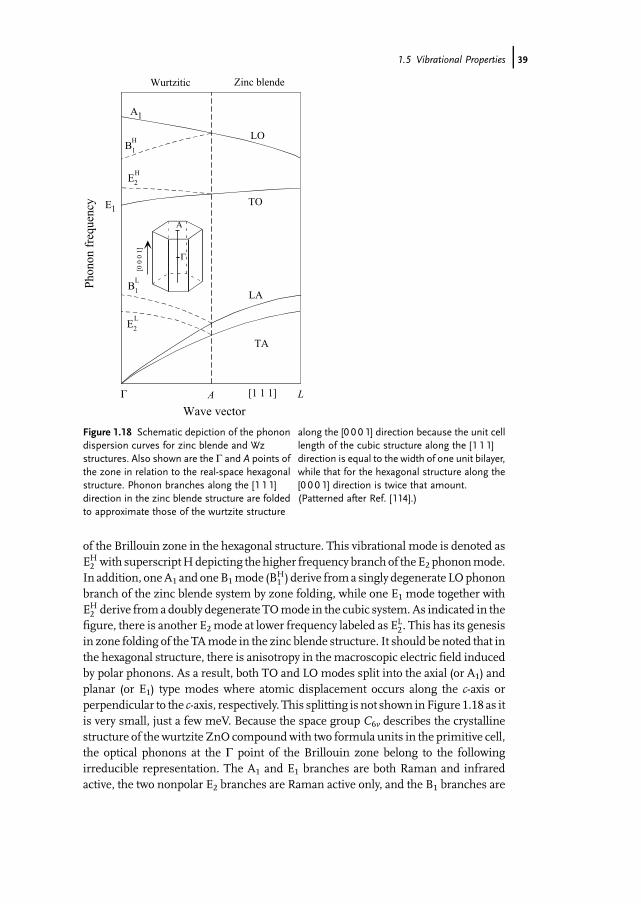
of the Brillouin zone in the hexagonal structure. This vibrational mode is denoted asEH2 with superscriptHdepicting thehigher frequency branch of theE2 phononmode.
In addition, oneA1 and oneB1mode (BH1 ) derive froma singly degenerate LOphonon
branch of the zinc blende system by zone folding, while one E1 mode together withEH2 derive from a doubly degenerate TOmode in the cubic system. As indicated in the
figure, there is another E2mode at lower frequency labeled as EL2. This has its genesis
in zone folding of the TAmode in the zinc blende structure. It should be noted that inthe hexagonal structure, there is anisotropy in the macroscopic electric field inducedby polar phonons. As a result, both TO and LO modes split into the axial (or A1) andplanar (or E1) type modes where atomic displacement occurs along the c-axis orperpendicular to the c-axis, respectively. This splitting is not shown inFigure 1.18 as itis very small, just a few meV. Because the space group C6v describes the crystallinestructure of thewurtzite ZnO compoundwith two formula units in the primitive cell,the optical phonons at the G point of the Brillouin zone belong to the followingirreducible representation. The A1 and E1 branches are both Raman and infraredactive, the two nonpolar E2 branches are Raman active only, and the B1 branches are
A
Γ
TA
LA
TO
LO
A1
A LΓ
Wurtzitic Zinc blende
E1
Phon
on f
requ
ency
Wave vector
[1 1 1]
B1
H
E2H
B1
L
E2
L
[0 0
0 1
]
Figure 1.18 Schematic depiction of the phonondispersion curves for zinc blende and Wzstructures. Also shown are the G and A points ofthe zone in relation to the real-space hexagonalstructure. Phonon branches along the [1 1 1]direction in the zinc blende structure are foldedto approximate those of the wurtzite structure
along the [0 0 0 1] direction because the unit celllength of the cubic structure along the [1 1 1]direction is equal to the width of one unit bilayer,while that for the hexagonal structure along the[0 0 0 1] direction is twice that amount.(Patterned after Ref. [114].)
1.5 Vibrational Properties j39

inactive (silent modes). The A1 and E1 modes are each split into LO and TOcomponents with different frequencies due to the macroscopic electric fieldsassociated with the LO phonons. Because the electrostatic forces dominate theanisotropy in the short-range forces, the TO–LO splitting is larger than the A1–E1splitting. For the lattice vibrations with A1 and E1 symmetry, the atomsmove paralleland perpendicular to the c-axis, respectively. The low-frequency E2mode is associatedwith the vibration of the heavy Zn sublattice, while the high-frequency E2 modeinvolves only the oxygen atoms. In the case of highly oriented ZnO films, if theincident light is exactly normal to the surface, only A1(LO) and E2modes are observedand the other modes are forbidden according to the Raman selection rules.The first-order phonon Raman scattering is due to phonons near the G point zone
center, that is, with wave vector k 0, because of themomentum conservation rule inthe light scattering process. Raman measurements are typically employed to probethe vibrational properties of semiconductors. When done along the directionperpendicular to the (0 0 0 1) plane, the nomenclature used to describe this confi-guration is depicted asZðXY ;XYÞ �Z.Here, followingPorto�s notation [105], A(B,C)Dis used to describe the Raman geometry and polarization where A and D representthe wave vector direction of the incoming and scattered light, respectively, whereas Band C represent the polarization of the incoming and scattered light. In Ramanscattering, all the above-mentioned modes, with the exception of B1 modes, areoptically active. Because of their polar nature, the A1 and E1 modes split intolongitudinal optical (A1-LO and E1-LO), meaning beating along the c-axis, andtransverse optical (A1-TO and E1-TO), meaning beating in the basal plane. Toreiterate, the A1 and B1 modes give atomic displacements along the c-axis, whilethe others, E1 andE2, give atomic displacements perpendicular to the c-axis,Here, theA1 and E1 modes are both Raman and IR active, while the two E2 modes are onlyRaman active, and the two B1modes are neither Raman nor IR active,meaning silentmodes. In the ZðXY ;XYÞ �Z configuration, only the E1
2 (or EL2 or E2-low), E
22 (or E
H2 or
E2-high), andA1(LO)modes should be observable. In particular, in theZðX ;XÞ �Z andZðY ;YÞ �Z geometries all three modes are observable, while in the ZðX ;YÞ �Z orZðY ;XÞ �Z geometries only the E2 modes are detected [106]. The details of themode–Raman configuration relationship are provided in Table 1.8. Shown inFigure 1.19 are the modes and the Raman backscattered geometries in relation tohexagonal crystalline orientation that can be used to sense the various phononmodesindicated.The acousticmodes are simple translationalmodes, and opticalmodes forwurtzite
symmetry are shown in Figure 1.20. Table 1.9 gives a list of observed zone centeroptical phonon wave numbers along with those calculated for wurtzite ZnO.The optical phonon energies are linked to the low- and high-frequency dielectric
constants and therefore can be calculated from one another. Electromagnetic theoryindicates that for any longitudinal electromagnetic wave to propagate, the dielectricfunction e(w) must vanish. Doing so leads to [113]
eðwÞeð¥Þ ¼
w2LO�w2
w2TO�w2
; ð1:27Þ
40j 1 General Properties of ZnO

wherewLO andwTO represent the LO and TO phonon frequencies, and e(w) and e(¥)represent the low and high (optical) frequency dielectric constants, respectively.When w¼wLO, the dielectric function vanishes, e(wLO)¼ 0. Equation 1.27 can beexpanded to the directional dependence of the dielectric function inwurtzite ZnO. Inthe direction parallel to the c-axis or the z-direction, from theG point to the Apoint, inthe k-space (with x, y representing the in-plane coordinates), the low- and high-frequency dielectric functions are related to each other with the help of A1(LO) andE1(TO) phonon frequencies through [119]
e==ðwÞ ¼ e¥==w2�w2
==ðLOÞw2�w2
==ðTOÞ: ð1:28Þ
Table 1.8 Raman measurement configuration needed to observethe phonon modes in hexagonal ZnO.
Mode Configuration
A1(TO), E2 XðY ;YÞ �XA1(TO) XðZ;ZÞ �XE1(TO) XðZ;YÞ �XE1(TO), E1(LO) XðY ;ZÞYE2 XðY ;YÞZE2 ZðY ;XÞ �ZA1(LO), E2 ZðY ;YÞ �Z
Y
X
ZSubstrate
ZnO
c-axis
Subs
trat
e
ZnO
c-axis
Y
Z
X
E2L
E2H
A1(LO)
X(Z,Z)X
X(Z,Y)X
A1(TO)
E1(TO)
Z(X,Y )Z+Z(X,X)Z
Figure 1.19 Schematic representation of two Ramanconfigurations with incident and scattered light directionsin the backscattering geometry for ZðX ;XÞ �Z þZðX ;YÞ �Zconfiguration to sense EL
2 , EH2 , and A1(LO) modes, XðZ;ZÞ �X
configuration to sense A1(TO) mode, and XðZ;YÞ �Xconfiguration to sense E1(TO) mode.
1.5 Vibrational Properties j41
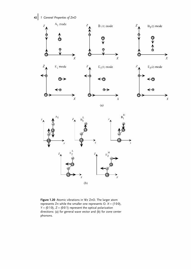
Figure 1.20 Atomic vibrations in Wz ZnO. The larger atomrepresents Zn while the smaller one represents O. X¼ (1 0 0),Y¼ (0 1 0), Z¼ (0 0 1) represent the optical polarizationdirections: (a) for general wave vector and (b) for zone centerphonons.
42j 1 General Properties of ZnO

Likewise, Equation 1.27 can be expanded in the direction perpendicular to thec-axis or the z-direction, or in the basal plane or the (x, y) plane (in k-space between theG point and M (1/2, 0, 0) or K (1/3, 1/3, 0) points). In this case, the low- and high-frequency dielectric functions are related to each other with the help of A1(TO) andE1(LO) phonons through [119]
e?ðwÞ ¼ e¥?w2�w2
?ðLOÞw2�w2
?ðTOÞ; ð1:29Þ
where ? and // indicate in the basal plane and along the c-direction, respectively.For wurtzite materials, the various directional components of phonon modes
correspond to w?(LO) ! E1(LO), wz(LO)¼w//(LO) ! A1(LO), w?(TO) ! E1(TO),and wz(TO)¼w//(TO) ! A1(TO). In the z-direction (along the c-direction) andthe directions perpendicular to the z-direction (in basal plane), LO and TO phononsare not mixed. For any direction other than these in-plane and out-of-plane
Table 1.9 Phononmode frequencies (in units of cm�1) of wurtziteZnO at the center of the Brillouin zone obtained from infraredspectroscopic ellipsometry (IRSE) and Raman scatteringmeasurements in comparison with theoretical predictions.
SymmetryRamanspectroscopy Infrared spectroscopy
Theoreticalcalculations
A1-TO 380 (2)a, 379 (2)b, 380c,380d, 378e, 380f
380g, 376.5j 382h, 386i
E1-TO 409 (2)a, 410 (2)b, 407c, 413d, 409.5e 409.1 (0.9)a, 408.2 (0.3)b,412g, 410.7j
316h, 407i
A1-LO 574c, 576e, 579d, 579f 574.5 (0.3)a, 577.1 (0.4)b,570g, 574.1j
548h
E1-LO 587 (2)a, 591 (2)b, 583c, 588e, 591d 588.3 (0.7)a, 592.1 (0.2)b,591g, 590.4j
628h
E2-low 102 (1)a, 102 (1)b, 101c, 101d, 98e, 99f 126h, 98i
E2-high 438 (1)a, 437 (1)b, 437c, 444d, 437.5e, 438f 335h, 433i
B1-low 261k
B1-high 552k
aZnO epilayer grown on sapphire. Error bars in parentheses of the infrared spectroscopy datarepresent the 90% confidence limits. Error bars of the Raman data are determined by theexperimental setup [123].bBulk ZnO. Error bars in parentheses represent the 90% confidence limits [123].cRaman scattering on ZnO single crystal [105].dRaman spectra on ZnO [106].eRaman spectra [121].fRaman spectra on ZnO film [115].gIR reflection [116].hAtomistic calculations based on an interatomic pair potential within the shell model approach [19].iCalculation [109].jGeneralized IRSE on a-plane ZnO on r-plane sapphire [117].kAb initio calculations [118].
1.5 Vibrational Properties j43

configurations, the LO and TO phonons mix and hybridize. For a given propagationdirection with an angle q relative to the c-axis (z-axis), one finds three phononbranches. One is an ordinary TO phonon mode with atomic displacement in the xyplane. The other two branches have amixed TO and LO character and their dielectricfunctions are given by the solutions of [120]
e== cos2 qþ e? sin2 q ¼ 0: ð1:30Þ
Using the above relationship, the phonon energy as a function of the angle caneasily be calculated. Doing so leads to the conclusion that the upper branch (LO-like) remains between the A1(LO) and E1(LO) energies while the lower branch (TO-like) remains between the A1(TO) and E1(TO) energies. Therefore, the dispersionremains small compared to the LO–TO separation, owing to the relatively small cellasymmetry and the large ionicity of atomic bonds. A more important consequenceof LO–TO mixing is that the TO-like mode couples to carriers whereas in the c-direction A1(LO) mode and in the basal plane E1(LO) phonons couple to thecarriers.For the special case w¼ 0 (or very small frequencies compared to the LO and TO
phonon frequencies), the relationship between the optical and static dielectricconstants reduces to the well-known Lyddane–Sach–Teller relationship
eðwÞeð¥Þ ¼
w2LO
w2TO
; ð1:31Þ
which is often used to determine the optical frequency dielectric constant fromknowledge of the A1(LO) and A1(TO) phonon frequencies along the c-direction andE1(LO) and E1(TO) in the basal plane. The static and high-frequency dielectricconstants of ZnO are listed in Table 3.8.A reasonably complete set of phonon mode frequencies has been measured by
using either IR or Raman spectroscopy (RS) for both bulk and thin-filmZnO. In earlymeasurements, phononmodes of bulk ZnOwere explored and discussed extensivelyby several groups using RS measurements [105–108, 121]. Observation of thephonon modes in PLD-grown ZnO thin films was reported by Lu et al. [122] andAshkenov et al. [117, 123]. No significant differences for the E1(TO), A1(TO), and E2mode frequencies were observed between the thin film and the bulk sample. Thethin-filmZnO phononmode frequencies are highly consistent with those of the bulkmaterial. A small redshift of the longitudinal optical phononmode frequencies of theZnO films with respect to the bulk material was tentatively assigned to the existenceof vacancy point defects within the films. The data obtained from IR and RSmeasurements are consistent with each other within the experimental accuracy.The predicted phonon frequencies reported by Tsuboi andWada [109] are also in verygood agreement with the experimental observations. The modes E1(TO) and A1(TO)reflect the strength of the polar lattice bonds. Accordingly, as discussed above nosignificant differences between the lattice constants of the film and bulk sampleswere observed.
44j 1 General Properties of ZnO

Figure 1.21 shows typical Raman spectra of the bulk and thin-film ZnO sam-ples [123]. In this particular study, solid lines in both figures indicate E1, A1, and E2phonon modes of ZnO. Dashed–dotted lines mark features observed at 332, 541,and 665 cm�1, which were assigned to possible multiple-phonon scattering proces-ses [105, 108]. Dotted lines are related to the sapphire phonon mode frequencies(A1g mode: 417 and 645 cm�1; Eg mode: 379, 430, 450, 578, and 751 cm�1) [110]. Forboth samples A1(LO) has not been observed and it was claimed that the scatteringcross section for this mode is markedly smaller than that of the A1(TO) mode due tothe destructive interference between the Fr€ohlich interaction and the deformationpotential contributions to the LO phonon scattering in ZnO [107]. Additionally, theoccurence of the E1(LO)mode in both samples was attributed to the breakdown of theselection rule due to the use of the Raman microscope.Rajalakshmi et al. [124] have reported additional Raman peaks at 205, 331, and
539 cm�1 in their ZnO nanoparticle samples synthesized at ambient temperatureusing an electrochemical cell. Similar peaks (208, 332, and 541 cm�1) that occurunder resonance conditions were also reported for bulk ZnO [108]. In both studies,these peaks have been assigned to the second-order Raman spectrum arising from
800700600500400300
z(xx)z′
z(xy)z′
ω (cm -1)
Ram
an in
tens
ity (
a.u.
)
x(yz)x′
x(yy)x′
x(zz)x′
E2(2)
(a) ZnOA1(TO)
E1(TO)
E1(LO)
(a)
800700600500400300
z(xy)z′
ω (cm-1)
z(xx)z′
x(yz)x′
Ram
an in
tens
ity (
a.u.
)
x(yy)x′
x(zz)x′
E2
(2)
(b) ZnO/
(b)
α-Al2O3
E1(LO)
E1(TO)
A1(TO)
Figure 1.21 (a) Raman spectra of the bulk ZnOsample. First-orderphononmodes of ZnOare indicated by the vertical solid lines. Thevertical dashed–dotted lines mark the features due to multiple-phonon scattering processes. (b) Raman spectra for the thin-filmZnO sample. The vertical dotted lines indicate the Raman-activesapphire substrate phonon mode frequencies. (Courtesy of M.Schubert [123].)
1.5 Vibrational Properties j45

zone boundary (M point) phonons 2-TA(M), 2-E2(M), and 2-LA(M), respectively.However, the coupling to plasmons in highly doped material and stress-inducedeffects due to lattice mismatch with the substrate might play a role in the interpreta-tion of the observed phonon frequencies.The hydrostatic pressure dependence of the zone center phonon modes has also
been studied. In conjunction with the previously reported results [111, 125],Decremps et al. [92] investigated in detail the pressure-induced Raman shifts in asingle-crystal ZnO sample at room temperature using Raman spectroscopy and abinitio calculations based on a plane-wave pseudopotential method within the densityfunctional theory. The pressure dependence of the zone center phonons (E2, A1, andE1) was measured for the wurtzite structure up to the hexagonal/cubic phasetransition pressure (�8.7GPa), above which all Raman peaks disappeared. Thepressure dependences of the phonon frequencies for the two high-pressure experi-ments are shown in Figure 1.22. Only the E2-lowmode exhibited a negative pressuredependence. The frequency shifts in the E2-high, A1(TO), E1(TO), and E1(LO)modes were observed to increase with pressure. The pressure dependence of theopticalmode energies was also comparedwith the prediction of amodel. No evidenceof an anomaly in the E2 and A1 mode behaviors before the phase transition
Figure 1.22 Top: (nLO� nTO) E1 phonon mode splitting versuspressure. Solid lines are linear least-square fits to the experimentalpoints. Bottom: Pressure dependence of the observed opticalphonons. Open (full) symbols: propagation of light perpendicular(parallel) to c-axis. (Courtesy of F. Decremps [92].)
46j 1 General Properties of ZnO

was detected. The corresponding perpendicular tensor component of the Born�stransverse dynamic charge e*T (Z* in table 1.6) is experimentally found to increaseunder compression as e*TðPÞ ¼ 2:02�6:4� 10�3 P, whereas calculations givee*TðPÞ ¼ 2:09�2:5� 10�3 P (in units of the elementary charge e, P in GPa). It hasalso been noted that the observation of optical phonons under pressure doesnot show any softening of the optic A1 and E2-high modes as theoreticallyexpected [126, 127]. Moreover, from both the experimental observation and thetheoretical calculations, the LO–TO splitting of the E1 phonon mode, whichdepends on the long-range electrostatic forces, has unusually shown weak pressuredependence. This behavior has been attributed to a small variation of the chemicalbond ionicity of wurtzite ZnO with pressure. Experimentally, the second-orderprocess observation (e.g., via optical phonon instabilities) could not be performedbecause the wurtzite-to-rocksalt first-order transition limits the pressure rangewithin which the wurtzite structure exists.The strong bond in ZnO and light O atoms result in high phonon frequencies and
limit the range of possibly observable impurity-related local vibrational modes(LVMs) to even lighter elements at higher frequencies. So far, a number of reportshave appeared for the infrared and Raman modes, which have been associated withlocal vibrational modes of impurities, dopants, and defect complexes. Kaschneret al. [128] have studied the influence of nitrogen, which is considered as a potentialacceptor in ZnO, on the lattice dynamics of ZnO. They investigated a series ofsamples grown by chemical vapor deposition (CVD) containing different nitrogenconcentrations. The Raman spectra revealed vibrational modes at 275, 510, 582, 643,and 856 cm�1 in addition to the host phonons of ZnO as discussed above. It has beenobserved that the intensity of these additional modes correlates linearly with thenitrogen concentration. Therefore, these modes were interpreted as local vibrationalmodes due to the vibrating nitrogen-related complexes. Bundesmann et al. [129] latermeasured the phonon modes of Fe-, Sb-, Al-, Ga-, and Li-doped ZnO thin films,grown by pulsed laser deposition (PLD) on c-plane sapphire substrates usingpolarized micro-Raman spectroscopy. Additional modes at about 277, 511, 583,and 644 cm�1, which had been assigned to N incorporation, were observed forintentionally doped Fe, Sb, and Al films [129]. The mode at 277 cm�1 was alsoobserved for Ga-doped films. Based on these observations, it has been stated thatthese modes cannot be related directly to N incorporation. Instead, the host latticedefects were suggested to be the origin of the additionalmodes [129]. This suggestionwas supported by theoretical considerations, which stated that defects related to theincorporation of dopants might result in breakdown of the selection rules, and silentmodes becomeRaman active [130]. Therefore, the above-addressed additionalmodescan be related to silent modes of ZnO.First-principles calculations based on density functional theory within the local
density approximation and the pseudopotential plane-wave method by Van deWalle [131] suggest that hydrogen atoms might act as shallow donors in ZnO. Ithas been argued that the incorporation of hydrogen accompanied by remarkablylarge relaxations of the surrounding atoms leads to anO–Hbond,which in fact can beregarded as a new type of dopant atom in ZnO. To determine the microscopic
1.5 Vibrational Properties j47

structure of hydrogen donors, the LVMs arising from these complexes have beeninvestigated using IR and Raman spectroscopy [132–134]. The hydrogen-relateddefects in ZnO samples, hydrogenated using an H or a D plasma, have beeninvestigated by a combination of local vibrational mode spectroscopy and comparedwith thefirst-principles calculations. Three new IR absorption lines at 3611.3, 3349.6,and 3312.2 cm�1 have been observed at 10 K. Based on polarization studies andfirst-principles calculations, the line at 3611.3 cm�1 was assigned to a singleinterstitial hydrogen atom at the bond center site oriented along the c-axis of thecrystal although the possibility that thisHatom is associated with an impurity cannotbe ruled out. The lines at 3349.6 and 3312.2 cm�1 were attributed to a zinc vacancythat contains two inequivalent hydrogen atoms, one in anO–Hbond roughly alignedwith the c-axis and the other in an O�H bond that forms an angle of 100� with thec-axis [133].McCluskey et al. [132] have also used IR spectroscopy to measure local vibrational
modes in ZnO annealed in hydrogen gas. An IR absorption peak at 3326.3 cm�1 wasobserved at a temperature of 8 K and attributed to the O–H stretch mode based oncomparison with the first-principles calculations of Van de Walle [131], in which thecalculated mode frequencies were 3726 and 3384 cm�1 for the bond-centered andantibonding configurations, respectively, after subtracting 166 cm�1 due to theanharmonic terms in the potential causing the stretch-mode frequency to shiftdownward. However, because of the uncertainty in actual anharmonicity the bond-centered configuration was not ruled out. The IR spectrum of ZnO annealed indeuterium has revealed an additional stretch mode at 2470.3 cm�1 for the sametemperature, which was tentatively assigned to the oxygen–deuterium (O–D) com-plexes. Using polarization measurements at room temperature, they also showedthat the dipole of the O–H complex does not lie parallel to the c-axis of wurtziteZnO [132, 135].Using Raman backscattering spectroscopy, Nickel and Fleischer [136] have de-
tected six local vibrational modes at 2854, 2890, 2918, 2948, 2988, and 3096 cm�1. ARaman backscattering spectrum measured on an as-grown ZnO single crystal isshown in Figure 1.23. The peak positions were obtained by deconvolving thespectrum into six Gaussian lines. To elucidate the origin of the local vibrationalmodes, Nickel and Fleischer performed hydrogen effusion experiments on ZnOsingle crystals. Upon annealing some samples up to 950 �C to remove hydrogen, thesubsequent measurement revealed that the local vibrational modes disappeared,from which the observed vibrational modes were attributed to the presence ofhydrogen in the ZnO crystals. It was found that the stretching vibration of thecorresponding hydrogen complex is not parallel to the c-axis. The vibrational modeslocated at 2854, 2890, 2918, 2948, and 2988 cm�1 were assumed to be due to thestretching modes of C–H, symmetric stretching modes of C–H3, symmetric stretch-ing modes of C–H2, antisymmetric stretching modes of C–H3, and antisymmetricstretching modes of C–H2, respectively, based on the effusion data, where asignificant concentration of hydrocarbons was detected. The local vibrational modelocated at 3096 cm�1 was attributed to the N–H, assuming a considerable amount ofhydrogen is bonded to nitrogen atoms based on the effusion experimental data. This
48j 1 General Properties of ZnO

observedmode frequencywas also found to be consistent with that reported for ZnSecompound semiconductors [137].
1.6Thermal Properties
As in all solids, the atoms in a semiconductor at nonzero temperature are in ceaselessmotion, oscillating about their equilibriumstates. These oscillationmodes are definedby phonons as discussed in Section 1.5. The amplitude of the vibrations increaseswithtemperature, and the thermal properties of the semiconductordetermine the responseof the material to temperature changes. Thermal expansion, specific heat, andpyroelectricity are among the standard material properties that define the linearrelationships between mechanical, electrical, and thermal variables. These thermalproperties and thermal conductivity depend on the ambient temperature, and theultimate temperature limit to study these effects is themelting temperature, which is�1975K forZnO. It should also be noted that because ZnO iswidely used in thin-filmform deposited on foreign substrates, meaning templates other than ZnO, theproperties of the ZnO films also intricately depend on the inherent properties of thesubstrates, such as lattice constants and thermal expansion coefficients.
Ram
an in
tens
ity (
a.u.
)
Angular frequency, ω (cm-1)
2854
28902918
2948
2988
3095
2800 2900 320031003000
Figure 1.23 Raman backscattering spectrum of as-grown single-crystal ZnO after background subtraction. The sample wasirradiated with the 488 nm line of an Ar laser and a power of190mW.The solid line represents a least-square fit of sixGaussianlines to the data. The dashed lines indicate the individual localvibrational modes. The peak positions are indicated in the plot.(Courtesy of N.H. Nickel [136].)
1.6 Thermal Properties j49

1.6.1Thermal Expansion Coefficients
The lattice parameters of semiconductors depend on temperature and are quantifiedby thermal expansion coefficients, which are denoted as Da/a oraa and Dc/c orac, forin-plane and out-of-plane cases, respectively. They depend on the stoichiometry,presence of extended defects, and free carrier concentration. The typical room-temperature values for ZnO are Da/a¼ 4.75� 10�6 K�1 and Dc/c¼ 2.9� 10�6 K�1
[138]. Figure 1.24 depicts the percent thermal expansion of ZnO in the c-plane andalong the c-axis as a function of temperature [139]. Also shown is the thermalexpansion of polycrystalline ZnO.The temperature dependence of the lattice constants a and c and the thermal
expansion coefficients of hexagonal ZnO have been determined by the capacitivemethod [138]. The thermal expansion coefficientsmeasured between 4 and 800K areshown in Figure 1.25. Reeber [30] has employed X-ray powder diffraction methodsinstead to measure the temperature dependence of the lattice parameters of ZnO inthe range of 4.2–296K. The results are shown in Figure 1.26. When analyzing thedependence of the lattice parameters on temperature, fourth-order polynomials
aðTÞ ¼ 3:248 53�1:0811� 10�5T þ 6:820� 10�8T2�6:109� 10�11T3
þ 2:143� 10�14T4 ð1:32Þwere fitted by using the least-square method, which gives a minimum for the a0parameter at 93K. The c0 parameter did not give anyminimum,most probably due toits low precision and uncertainty in the measurement. Using the same X-raydiffraction technique from 300 to 1373K for powdered ZnO crystals, Iwanagaet al. [140] obtained second-order polynomials for the temperature dependence of
1.0
0.8
0.6
0.4
0.2
0.0
-0.1200 400 600 1000800 1800160014001200 20000
Polycrystalline
1.2
c-axis
a-axis
(K)Temperature
The
rmal
expa
nsio
nco
effi
cien
t(%
)
Figure 1.24 Thermal expansion of ZnO in the c-plane (alongthe a-axis) and along the c-axis as a function of temperature.Also shown is the thermal expansion coefficient of polycrystallineZnO. (After Ref. [139].)
50j 1 General Properties of ZnO

the lattice parameters measured within an error of 5� 10�4 Å:
aðTÞ ¼ 3:2468þ 0:623� 10�5T þ 12:94� 10�9T2;
cðTÞ ¼ 5:2042þ 0:522� 10�5T þ 12:13� 10�9T2;ð1:33Þ
with corresponding thermal expansion coefficients of aa¼ 4.31� 10�6 K�1 andac¼ 2.49� 10�6 K�1 at 300K.Hang and Jou [141] studied thermal properties of ZnO films prepared by RF
magnetron sputtering on Si andGaAs substrates. Thermal stresses were determinedby using bending beam technique where the specimens were thermally cycled from25 to 400 �C. They investigated the thermal expansion coefficient as a function ofgrowth parameters, such as substrate temperature and sputtering power. With a
10008006004002000-20
0
20
40
60
80
100
150100500-10
0
10
α (1
0-7 K
-1)
Temperature (K)
αa
αc
α (1
0-7 K
-1)
Temperature (K)
αa
αc
Figure 1.25 Thermal expansion coefficientsaa (?c) andac (||c) ofZnO as a function of temperature. (After Ref. [138].)
3002001000
3.2478
3.2486
3.2494
3.2502
3.2510
3.2518
5.189
5.193
5.197
5.201
5.205
5.209
Lat
tice
para
met
ers
(Å)
Temperature (K)
a0
c0
Figure 1.26 Wurtzite ZnO lattice parameters as a function of temperature. (After Ref. [30].)
1.6 Thermal Properties j51
few exceptions, they found no significant changes with the variation of total gaspressure from 0.53 to 2.1 Pa, substrate temperature from 250 to 450 �C, Ar-to-O pre-ssure ratio from 0.3 to 3, and power from 100 to 300W. It has been observed that thethermal expansion coefficient increases about 37% from 5� 10�6 to 8� 10�6 �C�1
within the temperature range of 25–400 �C. Aoumeur et al. [100] calculatedthe thermal expansion coefficient for both zinc blende and rocksalt phases of ZnOusing a molecular dynamics simulation based on Tersoff�s potential. They foundthat a¼ 1.24� 10�5 K�1 for the zinc blende and a¼ 0.16� 10�5 K�1 for rocksaltstructures.As alluded to earlier, ZnO is widely used in thin-film form deposited on nonnative
substrates. Therefore, the material quality, actually properties in general, of the ZnOfilms depends on the properties of the substrates used. Especially, the latticeparameters and thermal expansion coefficients of these substrates are extremelyimportant since reduction of strain and dislocation density in ZnO thin films is themain objective, and substrates with parameters similar to those of ZnO are favorablein this context. Thermal expansion coefficients of various substrates used for thin-film ZnO growth are given in Table 2.3.
1.6.2Thermal Conductivity
Thermal conductivity (k), a kinetic property determined by the contributions fromthe vibrational, rotational, and electronic degrees of freedom, is an extremelyimportant material property when high-power/high-temperature electronic andoptoelectronic devices are considered. For pure crystals, phonon–phonon scattering,which is ideally proportional to T�1 above the Debye temperature, is the limitingprocess for thermal conductivity. Specifically, the heat transport is predominantlydetermined by the phonon–phonon Umklapp scattering and phonon scattering bypoint and extended defects, such as vacancies (inclusive of lattice distortions causedby them), impurities, and isotope fluctuations (mass fluctuation). As for othersemiconductors point defects play a significant role in thermal conductivity of ZnO.The lattice contribution (phonon scattering) to the thermal conductivity k is obtainedfrom the kinetic theory as [142]
klatticeðTÞ ¼ 13vsClatticeðTÞLðTÞ; ð1:34Þ
where T is the temperature, vs is the velocity of sound (almost independent oftemperature), Clattice(T ) is the lattice specific heat, and L(T ) is the phononmean freepath. In almost all materials, k(T ) first increases with temperature, reaches amaximum (kmax) at some characteristic temperature Tch, and then decreases. Atlow temperatures, L is relatively long and is dominated by extrinsic effects such as�defects� and/or finite crystal size and Clattice(T )� (T/qD)3, where qD is the Debyetemperature. As the temperature increases,Clattice(T ) begins to saturate and intrinsictemperature-dependent Umklapp processes become dominant, thus causing adecrease in L.
52j 1 General Properties of ZnO

The electronic contribution to the thermal conductivity, which is negligible forcarrier concentrations �1019 cm�3, is [143]
kelectrðTÞ ¼ p2nk2BTtelectr3m*
c; ð1:35Þ
where n is the carrier density, kB is the Boltzmann constant, telectr is the scatteringtime of the electrons, and m*
c is the conduction band effective mass. The overallthermal conductivity generally decreases with increasing carrier concentration,because the decrease in the lattice component of k due to increased phononscattering from both impurities and free electrons outweighs the increase in theelectronic contribution to k [144].Scanning thermal microscopy (SThM) [145] is a powerful technique used to
measure thermal conductivity and is purported to provide nondestructive, absolutemeasurements with a high spatial/depth resolution of about 2–3 mm. Thermalimaging is achieved by using a resistive thermal element incorporated at the end ofa cantilever/AFM tip, which forms one element of a Wheatstone bridge (for moreinformation and a schematic see Ref. [91]). Upon contact with the sample, the tiptends to cool down due to heat conduction into the sample, which is related to itsthermal conductivity, k. The bridge circuit applies a compensating voltage (Vout) tomaintain its target operating temperature. The feedback signal for constantresistance is a measure of the thermal conductivity of the material with whichthe tip is in contact, specificallyV2
out is proportional to k, because power dissipationis the mechanism here. Measurements of the absolute values of k are based on acalibration procedure. This simply comprises calibrating the feedback signal, V2
out,for a constant thermal element resistance against that for samples with knownconductivities such as GaSb, GaAs, InP, Si, and Al metal. The influence of thesurface roughness on the effective thermal conductivity is of concern. For aperfectly flat surface, the contact between the probe tip (radius of curvature�1 mm)and the sample surface is very small. However, for rough surfaces the tip couldimpinge on a valley- or hillock-like feature with the result that a valley/hillock willlead to increased/decreased thermal signal with a corresponding change in themeasured effective thermal conductivity.SThM was applied to measure the room-temperature thermal conductivity on Zn
and O faces of high-quality ZnO (0 0 0 1) single crystals, grown by a vapor-phasetransportmethod [146]. The thermal investigation was performed in twoways: point-by-point (�2mm resolution) and area scans. The point-by-point measurements onZn-face samples producedk¼ 1.16� 0.08 and 1.02� 0.07Wcm�1 K�1, whileO-facesamples showed k¼ 1.10� 0.09 and 0.98� 0.08Wcm�1 K�1. The variations repre-sent the standard deviation in the data, which was obtained by investigatingapproximately 15–20 points randomly distributed over a 6� 6mm2 surface area.In this study, a correlation between the surface topography and thermal conductivityvariations was also studied by acquiring the AFM and SThM scans simultaneouslyduring the area scan. The effects of surface roughness on effective k valueswere treated in terms of tip–surface geometry. It has been argued that when the
1.6 Thermal Properties j53

experimental voltage variations (proportional to k) correspond to only 6–7% changesin the thermal conductivity, variations probably originate from the topography. Largervariations (>12%) in the SThM voltage reading for AFM topographical features withheights <100 nm would be an indication of intrinsic thermal conductivity variationsacross the area under investigation.Pollak and coworkers [147] measured the thermal conductivity k of several bulk
ZnO (0 0 0 1) samples grown by CERMET, Inc. and prepared by the authors� groupunder different surface treatments. The measurements were made using SThMwith a spatial/depth resolution of about 2–3mm. The surface treatments of varioussamples are summarized in Table 1.10. The measurements were made at differentpoints on each sample and the results are also shown in Table 1.10. For sample (a)in both positions, k is considerably less than the previously reported values ofabout 1.0Wcm�1 K�1 [146]. To be consistent with the earlier models, one wouldargue that forming gas annealing has resulted in surface roughness, which hasconsiderably reduced k. The same is mostly true for sample (e), which exhibitsconsiderable inhomogeneity in the measured k. At present, there is no explanationfor this result, although Florescu et al. [144] did find that in GaN k was a functionof carrier concentration; that is, it decreased with increasing carrier concentrationdue to scattering of phonons from the ionized impurities. No information isavailable neither about the carrier concentrations/doping levels nor about theirdistribution for this or any other of the samples. For sample (b) the measuredresults for k are similar to those reported in Ref. [146], while for samples (c) and(d) they are actually somewhat higher and are the highest k values reported forZnO. Thus, both air annealing and nitrogen plasma treatment result in a goodsurface.
Table 1.10 Thermal conductivity, k (W cm�1 K�1), at multiplepositions of bulk ZnO samples with various surface treatments[147].
Sample Surface treatment Thermal conductivity (W cm�1 K�1)
(a) Forming gas annealed (1) k¼ 0.67� 0.08(2) k¼ 0.46� 0.05
(b) As received (O face) (1) k¼ 1.00� 0.08(2) k¼ 0.95� 0.06
(c) Air annealed (1) k¼ 1.35� 0.08(2) k¼ 1.25� 0.05
(d) Nitrogen plasma treated at 750 �C (1) k¼ 1.44� 0.08(2) k¼ 1.47� 0.08
(e) Oxygen plasma treated at 700 �C (1) k¼ 0.87� 0.06(2) k¼ 0.75� 0.06(3) k¼ 0.80� 0.06(4) k¼ 1.24� 0.05(5) k¼ 0.54� 0.07
54j 1 General Properties of ZnO

Olorunyolemi et al. [148] measured the thermal conductivity of ZnO powders withdifferent particle sizes (micrometer, submicrometer, and nanometer) from theas-received powder state to fully sintered state by using a laser flash technique.Curves of thermal conductivity versus temperature for the three sets of ZnO samples(micrometer, submicrometer, and nanometer) measured as they were heated to600 �C and cooled back to 25 �C are shown in Figure 1.27. The first surprisingobservation is that the thermal conductivity at room temperature and up to 200 �C isthe reverse of what is expected for the different particle sizes, with the nanopowderhaving the highest thermal conductivity. The room-temperature thermal conductivi-ties were measured to be 0.745, 0.914, and 1.160Wm�1 K�1 for micro-, submicron-,and nanosized samples with an average particle diameter of 1.0mm, 0.2mm, and20 nm, respectively. The initial higher thermal conductivity of the nanopowder ZnOsamples was attributed to the adsorbed water including chemisorbed water (morethan that adsorbed by the submicrometer, which in turn is more than that adsorbedby themicrometer powder). Above 400 �C, the thermal conductivity of the nanosizedparticle increases faster with increasing temperature than that of the submicrometer-and the micrometer-sized samples. In this work, a model for interparticle neckgrowth was also developed based on themass transfer of a powder to the neck regionas a result of known temperature. The observed data were compared with thetheoretical results obtained by the three-dimensional numerical code combinedwith this model.Figure 1.28 shows the measured thermal conductivity of a fully sintered sample
heated from room temperature to 1000 �C. The thermal conductivity decreases from37 to 4Wm�1 K�1 as the temperature is increased from room temperature to1000 �C. This is the thermal conductivity curve for a fully dense ZnO crystal, where
0.0
1.0
2.0
3.0
4.0
5.0
6.0
7.0
8.0
9.0
10
6005004003002001000
NanoSubmicronMicron
Cooling
Heating
(Temperature ºC)
Mea
sure
d th
erm
al c
ondu
ctiv
ity(W
m-1
K-1
)
Figure 1.27 Thermal conductivity of nanometer-, submicrometer-,and micrometer-sized ZnO heated from room temperature to600 �C at 3 �Cmin�1. (After Ref. [148].)
1.6 Thermal Properties j55

the resistive phonon–phonon interactions (Umklapp processes) are the dominantscattering mechanisms.The thermal properties of ZnO doped with Al and Mg were also studied by a
number of groups [149–153] for the evaluation of the thermoelectric performance.Tsubota et al. [152] investigated the thermal conductivity of sintered(Zn1�yMgy)1�xAlxO (x¼ 0–0.1, y¼ 0–0.1) samples determined from thermaldiffusivity and specific heat capacity measured by the laser flash technique anddifferential scanning calorimetry (DSC), respectively. The temperature depen-dences of the thermal conductivities of (Zn1�yMgy)0.98Al0.02O (y¼ 0, 0.02, 0.1) areshown in Figure 1.29 in comparison with that of ZnO. The reduction of k from
100080060040020000
10
20
30
40
The
rmal
con
duct
ivity
(W
m-1
K-1
)
Temperature (ºC)
Figure 1.28 Thermal conductivity of fully sintered ZnO heatedfrom room temperature to 1000 �C. (After Ref. [148].)
43210
10
20
30
40
50
The
rmal
con
duct
ivity
(W
m-1
K-1
)
1/T (10-3 K-1)
Figure 1.29 Thermal conductivities of ZnO (diamonds),Zn0.98Al0.02O (triangles), and (Zn1�yMgy)0.98Al0.02O for y¼ 0.02(squares) and 0.1 (circles) as a function of inverse temperature.(After Ref. [152].)
56j 1 General Properties of ZnO

ZnO to Zn0.98Al0.02O was almost negligible. Although addition of Al (using Al2O3)is considered to be ineffective in suppressing k of ZnO-based materials, thedifference in k values between the MgO added samples and the Zn0.98Al0.02Osample is significantly larger at low temperatures, indicating that the addition ofMgO is very effective in reducing the thermal conductivity at low temperatures.From the temperature dependence behavior (1/T dependence above the Debyetemperature), the authors have concluded that the decrease in phonon–phononscattering contribution is mainly responsible for the reduction of thermal con-ductivity upon the addition of MgO as well as Al2O3. The formation of a solidsolution of MgO and ZnO is thereby considered to be effective in introducingphonon scattering centers to reduce vibrational component and thus the overallvalue of k.Similarly, thermal properties of (Zn1�yMgy)1�xAlxO (0 < x < 0.05 and 0 < y
0.16) ceramics synthesized from a powder precursor prepared by a polymerizedcomplex method have also been investigated by Katsuyama et al. [151]. Theyobserved similar dependence of thermal conductivity on temperature and dopingconstituents as Tsubota et al. [152]. The thermal conductivity decreased withincreasing x, but it was further suppressed by the additional substitution of theZn sites by Mg atoms with the resultant lattice contribution, that is, the pointdefects introduced by the addition of Mg enhanced the phonon scattering.However, in both studies, although the temperature dependence reveals 1/Tbehavior indicative of Umklapp scattering, room-temperature thermal conductiv-ity of sintered ZnO, which is about 40Wm�1 K�1 and reduces to �7Wm�1 K�1
with increasing MgO concentration, is much smaller than the values reportedfor the high-quality single crystal discussed above. This indicates the largecontribution due to enhanced phonon-point defect or -extended defect and-grain boundary scattering.Because ZnO thin films deposited on foreign substrates are used in different
applications, thermal conductivities of the substrates would be of concern whendesigning device structures. A comparison of thermal conductivities for varioustemplates used for ZnO growth is provided in Table 2.3.
1.6.3Specific Heat
The specific heat of a semiconductor has contributions from lattice vibrations, freecarriers (very effective at low temperatures), and point and extended defects. Forgood quality semi-insulating crystal, the specific heat is determined mostly by thelattice vibrations. The available specific heat data for ZnO is very limited. Lawlessand Gupta [154] investigated the specific heat for both pure and varistor type ofZnO samples between the temperature ranges of 1.7–25 K, where the latter hasan average grain size of 10 mm. Specific heat measurements were performedusing the pulse method. As seen in Figure 1.30, the specific heat of varistor ZnOdiverges from that of pure ZnO below 20 K. This difference was attributed to the
1.6 Thermal Properties j57

contribution by the large amount of impurities, present in the region of the grainboundaries of varistor-type ZnO, giving rise to a very large excess specific heatbelow 20 K.The specific heat data for pure ZnOwere further analyzed by considering two non-
Debye features at different temperature regions according to
C ¼ CDebye þCSchottky þCEinstein; ð1:36Þ
where CDebye, CSchottky, and CEinstein represent the Debye, Schottky, and Einsteinterms of the total specific heat of ZnO, respectively. In general, the Debye expressionfor the temperature dependence of specific heat in a solid at a constant pressure canbe expressed as
CDebye ¼ 18RTqD
� �3
:
ðxD0
x4ex
ðex�1Þ2 dx; ð1:37Þ
where xD� qD/T and R¼ 8.3144 Jmol�1 K�1 is the molar gas constant. The coeffi-cient in front of the term R has been multiplied by 2 to take into account the twoconstituents making up the binary compound. By fitting the measured tempera-ture-dependent heat capacity to the Debye expression, one can obtain the Debyetemperature qD specific to the heat capacity. It is often easier to extract a Debyetemperature by using data either near very low temperatures or well below
Temperature (K)
Spec
ific
hea
t, C
(er
gg
-1K
-1)
Varistor
Pure
θD K= 399.5
105
104
102
103
21 20105 30
Figure 1.30 Specific heat data measured for pure ZnO comparedto data for varistor ZnO. (After Ref. [154].)
58j 1 General Properties of ZnO

the Debye temperature where the specific heat has a simple cubic dependence ontemperature:
CDebye ¼ 234RTqD
� �3
: ð1:38Þ
Unfortunately for ZnO, the samples contain large densities of free carriers anddefects, which make the Debye specific heat expression unreliable. The Debyecontribution to the specific heat of pure ZnO is also shown in Figure 1.30 as thecurve labeled with a calorimetric Debye temperature of qD¼ 399.5 K, and thedeviation of the data below �5 K is due to the Schottky term and that above �10 Kis due to the Einstein term. The latter has an exponential dependence and isgiven by
CEinstein ¼ 3RrEqET
� �2
exp � qET
� �for T qE; ð1:39Þ
where rE is the number of Einstein oscillators per formula weight and qE is theEinstein temperature. Schottky term has a T�2 dependence and is expressed by
CSchottky ¼ bT�2; ð1:40Þ
where b¼ nR(d/2)2 (n¼ rE is assumed) is the Schottky coefficient.The least-square fits of these two expressions to the experimental data for the
corresponding temperature ranges are shown in Figure 1.31. Very good agreementwith 2–3% uncertainty was achieved for the values of qE¼ 120.5 K and rE¼ 8.72� 10�2 for the case of Einstein model and b¼ 350.7 erg g�1 K�1 for the Schottkyterm. The Zn interstitials (3.6� 1021 cm�3) might be responsible for the disper-sionless Einstein-type contribution to the specific heat above 10 K, whereas theSchottky contribution appearing below 4 K is due to ordering of, possibly, Zninterstitials with a characteristic energy of d¼ 1.1� 105 eV for such an orderingmechanism.
1.6.4Pyroelectricity
Pyroelectricity is a first-rank tensor property that relates the change in temperatureto a change in electrical displacement D (or polarization P since no field isapplied):
dDi ¼ dPi ¼ pidT or pi ¼ ðdPi=dTÞE : ð1:41Þ
The constraint for obtaining the pyroelectric coefficient pi (units Cm�2 K�1) isconstant electric field E. Under constant strain, that is, when the sample is rigidly
1.6 Thermal Properties j59
clamped to prevent thermal expansion or contraction, measurements reveal the�primary� pyroelectric coefficient, which originates from the change in the electricdisplacement due to internal rearrangements in the structure. However, most of themeasurements are carried out under constant stress, meaning that the crystaldeformation through thermal expansion is allowed. In this so-called �secondary�effect, the strain induced by thermal expansion alters the electric displacementthrough the piezoelectric process because all pyroelectric materials are also piezo-electric, such as ZnO. To exhibit pyroelectricity, the material should have no central
5432100
1
2
3
4
CT
2 (10
4 erg
g-1 K
)
T (10 K )5 3 5
(a)
9876543
0.1
1
10
(b)
T2 C
ex/3
R
100/T (K-1
)
Figure 1.31 Fit to the pure ZnO data (a) using the Schottkymodel(with just Schottky and Debye contributions yielding a Debyetemperature of 395.5 K) and (b) using the Einstein model. Cex isthe excess specific heat (ideally the Einstein contribution)obtained by removing the Debye and Schottky contributions fromthe total specific heat. The Einstein oscillators are identified as theZn interstitials. (After Ref. [154].)
60j 1 General Properties of ZnO

symmetry, should have either no axis of rotational symmetry or a single axis ofrotational symmetry that is not in an inversion axis, and its molecular structureshould have a nonzero dipole moment.The primary and the secondary pyroelectric effects are indicated in thewell-known
triangular diagram of Figure 1.32, which describes the pathways between themechanical, electrical, and thermal energies. Measurement of the primary effectis extremely difficult as it is difficult to prevent the thermal expansion completely. Thesecondary effect, however, can easily be calculated by using the elastic stiffness andpiezoelectric constants and the thermal expansion coefficient. The total (unclamped)pyroelectric coefficient (defined for constant stress as well as constant electric field) isgiven by the sum of the primary and secondary components and is what is usuallymeasured in experiments. Pyroelectric coefficients measured for various materialsare listed in Table 1.11 [155–157]. The pyroelectric effect is stronger in ferroelectricmaterials, which below a critical temperature, called the Curie temperature, exhibitstrong hysteretic electrical polarization, the direction of which can be reversed by anapplied electric field. Especially in ferroelectrics, the primary contribution to thepyroelectricity is generally larger than the secondary effect. In nonferroelectric orweakly ferroelectric materials such as ZnO, the pyroelectric coefficients are usuallysmall and correlate well with the specific heat, which is also caused by thermalmotions, as illustrated in Figure 1.33. In single-crystal hexagonal ZnO, the electric
Electrical
ThermalMechanical
Elec
trom
echa
nica
l
Electrothermal
Thermoelastic
Piezoe
lectri
city
Con
vers
epi
ezoe
lect
rici
ty
Perm
ittiv
ity
Electrocaloric
Primary
pyroelectricity
Heat capacity
deformationofHeat
σ T
E
Elasticity Thermal expansion
Piezocaloric
ε S
D
Secondary pyroelectricity
Figure 1.32 The well-known triangle used todescribe the pathways between mechanical,electrical, and thermal energies in a class ofnoncentrosymmetric materials exhibitingpiezoelectric effect, pyroelectric effect (converseof electrocaloric effect), piezocaloric effect(converse of thermal expansion), and so on. For
simplicity, the magnetic property node is notshown. The variables denoted as the nodes arestress (s), strain (e), electric field (E),displacement (D), temperature (T), and entropy(S). The primary (T to D) and secondary (T to eto D) pyroelectric effects are indicated.
1.6 Thermal Properties j61

40030020010000.0
0.5
1.0
0
5
10
Pyro
elec
tric
coe
ffic
ient
(nC
cm
-2 K
-1)
Temperature (K)
Spei
fic
heat
(ca
l mol
-1 K
-1)
Figure 1.33 Pyroelectric coefficient and specific heat of ZnOas a function of temperature. (After Ref. [156].)
Table 1.11 Primary, secondary, and total (experimentallymeasured) pyroelectric coefficients (in units of mCm�2 K�1)for various materials.
Primary coefficient Secondary coefficient Total (experimental value)
FerroelectricsPoled ceramics
BaTiO3 �260 þ60 �200PbZr0.95Ti0.05O3 �305.7 þ37.7 �268
CrystalsLiNbO3 �95.8 þ12.8 �83LiTaO3 �175 �1 �176Pb5Ge3O11 �110.5 þ15.5 �95Ba2NaNb5O15 �141.7 þ41.7 �100Sr0.5Ba0.5Nb2O6 �502 �48 �550(CH2CF2)n �14 �13 �27Triglycine sulfate (TGS) þ60 �330 �270Pb(Zr0.54Ti0.46)O3 �700PbTiO3 �1250
Nonferroelectrics and weak ferroelectricsZnO �6.9 �2.5 �9.4ZnO [157] �10.5CdSe �2.94 �0.56 �3.5CdS �3.0 �1.0 �4.0Tourmaline �0.48 �3.52 �4.0Li2SO4�2H2O þ60.2 þ26.1 þ86.3
From Refs [155–157].
62j 1 General Properties of ZnO
dipoles formed by the cations and anions add up as all the tetrahedral units pointalong the c-axis.
1.7Electrical Properties of Undoped ZnO
As a direct and large bandgap material, ZnO is attracting much attention for avariety of electronic and optoelectronic applications. Advantages associated with alarge bandgap include high-temperature and high-power operation, lower noisegeneration, higher breakdown voltages, and ability to sustain large electric fields.The electron transport in semiconductors can be considered for low and highelectric fields. (i) At sufficiently low electric fields, the energy gained by the electronsfrom the applied electric field is small compared to the thermal energy of electronsand therefore the energy distribution of electrons is unaffected by such a low electricfield. Because the scattering rates determining the electron mobility depend on theelectron distribution function, electronmobility remains independent of the appliedelectric field, and Ohm�s law is obeyed. (ii) When the electric field is increased to apoint where the energy gained by electrons from the external field is no longernegligible compared to the thermal energy of the electron, the electron distributionfunction changes significantly from its equilibrium value. These electrons becomehot electrons characterized by an electron temperature larger than the latticetemperature. Furthermore, as the dimensions of the device are decreased tosubmicron range, transient transport occurs when there is minimal or no energyloss to the lattice during a short and critical period of time, such as during transportunder the gate of a field effect transitor or through the base of bipolar transistor. Thetransient transport is characterized by the onset of ballistic or velocity overshootphenomenon. Because the electron drift velocity is higher than its steady-state value,one can design a device operating at frequencies exceeding those expected fromlinear scaling of dimensions.
1.7.1Low-Field Transport
Hall effect is themost widely used technique tomeasure the transport properties andassess the quality of epitaxial layers. For semiconductormaterials, it yields the carrierconcentration, its type, and carrier mobility. More specifically, experimental data onHall measurements over a wide temperature range (4.2–300K) provide quantitativeinformation on impurities, imperfections, uniformity, scattering mechanisms, andso on. TheHall coefficient and resistivity (r) are experimentally determined and thenrelated to the electrical parameters through (for n-type conduction) RH¼ rH/ne andmH¼RH/r, where n is the free electron concentration, e is the unit electronic charge,mH is the Hall mobility, and rH is the Hall scattering factor that depends on theparticular scattering mechanism. The drift mobility is the average velocity per unitelectric field in the limit of zero electric field and is related to the Hall mobility
1.7 Electrical Properties of Undoped ZnO j63

through the Hall scattering factor by mH¼ rHm. As noted above, the Hall scatteringfactor depends on the details of the scattering mechanism, which limits the driftvelocity. In degenerate semiconductors, the Hall factor is unity making the Hallmobility and drift mobility identical such as the case in FETs relying on 2D electrongas. As the carriers travel through a semiconductor, they encounter various scatteringmechanisms that govern the carriermobility in the electronic system. The parameterfor characterizing the various scattering mechanisms is the relaxation time t, whichdetermines the rate of change in electron momentum as it moves in the semicon-ductor crystal. Mobility is related to the scattering time by
m ¼ qhtim*
; ð1:42Þ
where m is the electron effective mass, q is the electronic charge, and hti is therelaxation time averaged over the energy distribution of electrons. The total relaxationtime, tT, when various scattering mechanisms are operative, is given byMatthiessen�s rule:
1tT
¼Xi
1ti; ð1:43Þ
where i represents each scattering process, provided that electron while undergoingone scattering event is not simultaneously affected by another.The major scattering mechanisms that generally govern the electron transport in
III–V semiconductors are also valid for ZnO. They are briefly listed as follows:
(i) Ionized impurity scattering is due to deflection of free carriers by the long-rangeCoulomb potentials of the charged centers caused by defects or intentionallydoped impurities. This can be thought as a local perturbation of the band edge,which affects the electron motion.
(ii) Polar longitudinal optical phonon scattering is caused by the interaction of amoving charge with an electric field induced by electric polarization associatedwith lattice vibration due to ionic nature of the bonds in a polar semiconductor.
(iii) Acoustic phonon scattering through deformation potential arises from theenergy change of the band edges induced by strain associated with acousticphonons, where the scattering rate increases with the wave vectors of thephonons.
(iv) Piezoelectric scattering arises from the electric fields that are produced by thestrain associated with phonons in a crystal without inversion symmetry.
(v) If the density of dislocations and native defects are high in a semiconductor,dislocation scattering and scattering through defects are also considered aspossible scattering mechanisms. Dislocation scattering is due to the fact thatacceptor centers are introduced along the dislocation line, which captureelectrons from the conduction band in an n-type semiconductor. Thedislocation lines become negatively charged and a space charge region is
64j 1 General Properties of ZnO
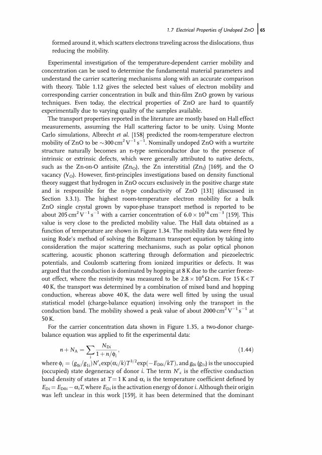
formed around it, which scatters electrons traveling across the dislocations, thusreducing the mobility.
Experimental investigation of the temperature-dependent carrier mobility andconcentration can be used to determine the fundamental material parameters andunderstand the carrier scattering mechanisms along with an accurate comparisonwith theory. Table 1.12 gives the selected best values of electron mobility andcorresponding carrier concentration in bulk and thin-film ZnO grown by varioustechniques. Even today, the electrical properties of ZnO are hard to quantifyexperimentally due to varying quality of the samples available.The transport properties reported in the literature are mostly based on Hall effect
measurements, assuming the Hall scattering factor to be unity. Using MonteCarlo simulations, Albrecht et al. [158] predicted the room-temperature electronmobility of ZnO to be �300 cm2V�1 s�1. Nominally undoped ZnO with a wurtzitestructure naturally becomes an n-type semiconductor due to the presence ofintrinsic or extrinsic defects, which were generally attributed to native defects,such as the Zn-on-O antisite (ZnO), the Zn interstitial (ZnI) [169], and the Ovacancy (VO). However, first-principles investigations based on density functionaltheory suggest that hydrogen in ZnO occurs exclusively in the positive charge stateand is responsible for the n-type conductivity of ZnO [131] (discussed inSection 3.3.1). The highest room-temperature electron mobility for a bulkZnO single crystal grown by vapor-phase transport method is reported to beabout 205 cm2V�1 s�1 with a carrier concentration of 6.0� 1016 cm�3 [159]. Thisvalue is very close to the predicted mobility value. The Hall data obtained as afunction of temperature are shown in Figure 1.34. The mobility data were fitted byusing Rode�s method of solving the Boltzmann transport equation by taking intoconsideration the major scattering mechanisms, such as polar optical phononscattering, acoustic phonon scattering through deformation and piezoelectricpotentials, and Coulomb scattering from ionized impurities or defects. It wasargued that the conduction is dominated by hopping at 8 K due to the carrier freeze-out effect, where the resistivity was measured to be 2.8� 104W cm. For 15K <T40K, the transport was determined by a combination of mixed band and hoppingconduction, whereas above 40K, the data were well fitted by using the usualstatistical model (charge-balance equation) involving only the transport in theconduction band. The mobility showed a peak value of about 2000 cm2V�1 s�1 at50 K.For the carrier concentration data shown in Figure 1.35, a two-donor charge-
balance equation was applied to fit the experimental data:
nþNA ¼Xi
NDi
1þ n=fi; ð1:44Þ
where fi ¼ ðg0i=g1iÞN 0cexpðai=kÞT3=2expð�ED0i=kTÞ, and g0i (g1i) is the unoccupied
(occupied) state degeneracy of donor i. The term N 0c is the effective conduction
band density of states at T¼ 1 K and ai is the temperature coefficient defined byEDi¼ED0i�aiT, where EDi is the activation energy of donor i. Although their originwas left unclear in this work [159], it has been determined that the dominant
1.7 Electrical Properties of Undoped ZnO j65

Table1.12
Acompilatio
nof
XRDresults,electronmob
ilitie
s,an
dcorrespo
ndingcarriercon
centratio
nsob
tained
inno
minallyun
dope
dbu
lkan
dthin-film
ZnO
depo
sitedon
differen
tsubstrates
byvariou
sgrow
thtechniqu
es.
Sample
FWHM
ofXR
Drockingcurves
(arcsec)
Carrie
rconcentration
(cm
�3 )
Electron
mob
ility
(cm
2V�
1s�
1 )References
Mon
teCarlo
calculation
——
300
[158
]Bulk
ZnO
grow
nby
vapo
r-ph
ase
tran
sportmethod
n/a
6.0·10
16
205
[159
]
Bulk
ZnO
grow
nby
pressurizedmeltmethod
49(0002)
5.05
·10
17(296
K),
3.64
·10
16
(77K)
131(296
K),
298(77K)
[160
]
Bulk
ZnO
grow
nby
hydrothermal
method
18(0002)
8·10
13(Licompensated)
200
[161]
ZnO
thin
film
sgrow
non
c-plan
esapp
hire
substrates
byPLD
151(0002)
2.0·10
16
155
[162
]
ZnO
thin
film
sgrow
non
c-plan
esapp
hire
grow
nby
MBE
42(0002)
1.2·10
17
130
[163
]
ZnO
thin
film
sgrow
non
a-plan
esapp
hireby
MBE
n/a
7.0·10
16
120
[164
]
Zn0.9Mn0.1O/Z
nO
heterostructure
grow
non
c-plan
esapp
hireby
PLD
n/a
8.8·10
12(areal
concentrationcm
�2 )
130
[165
]
ZnO
thin
film
sgrow
non
c-plan
esapp
hire
withZnO/M
gOdo
uble-buffer
layers
grow
nby
MBE
18(0002),1
076ð1
01�1Þ
1.2·10
17
145
[166
,167
]
ZnO
thin
film
sgrow
non
MgZ
nO-buffered
ScAlM
gO4substrates
byPLD
<12
(0002),<
12ð1
01�1Þ
1·10
16
440
[168
]
66j 1 General Properties of ZnO
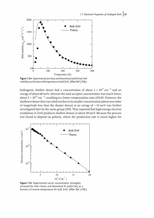
hydrogenic shallow donor had a concentration of about 1� 1017 cm�3 and anenergy of about 60meV, whereas the total acceptor concentration was much lower,about 2� 1015 cm�3, resulting in a lower compensation ratio of 0.02. However, theshallower donor that was ruled out due to its smaller concentration (about one orderof magnitude less than the deeper donor) at an energy of �31meV was furtherinvestigated later by the same group [169]. They reported that high-energy electronirradiation in ZnO produces shallow donors at about 30meV. Because the processwas found to depend on polarity, where the production rate is much higher for
40030020010000
500
1000
1500
2000
Bulk ZnO
Theory
Hal
l mob
ility
, µH
(cm
2 V
-1 s-1
)
Temperature (K)
Figure 1.34 Experimental (circles) and theoretical (solid line)Hallmobilityasa functionof temperature inbulkZnO.(AfterRef. [159].)
2015105
1015
1016
1017
Bulk ZnO
Theory
Ele
ctro
n co
ncen
trat
ion,
n (
cm-3)
103/T (K
-1)
Figure 1.35 Experimental carrier concentration (triangles)corrected for Hall r-factor and theoretical fit (solid line) as afunction of inverse temperature for bulk ZnO. (After Ref. [159].)
1.7 Electrical Properties of Undoped ZnO j67

Zn-face [0 0 0 1] than O-face ½0 0 0 1�� irradiation, it has been concluded that thisnative shallower donor is related to a Zn sublattice defect,most likely the interstitialZnI or a ZnI-related complex.Regarding the ZnO epilayers grown by various growth techniques on different
substrates, room-temperature mobilities are relatively poor [170] (typically below100 cm2V�1 s�1) compared to bulk ZnO, particularly the variety grown by the vapor-phase transport method. However, as listed in Table 1.12, some room-temperaturemobility values are comparable to the best reported value for bulk ZnO. Kaidashevet al. [162] reported the best reproducible electron mobilities from 115 up to155 cm2V�1 s�1 at 300K in a narrow carrier concentration range from 2 to 5� 1016
cm�3 for nominally undoped ZnO thin films of total thickness of 1–2mmgrown on c-plane sapphire substrates by amultistep PLD technique. They attributed this successto the multistep PLD process, which includes the insertion of 30 nm thin ZnOrelaxation layers deposited at a reduced substrate temperature. The topographicalproperties of the films were correlated with the corresponding electrical properties.The high-mobility samples showed atomicallyflat surface structure with grain size ofabout 0.5–1mm, whereas the surfaces of low-mobility films consisted of clearlyresolved hexagonally faceted columnar grains of only 200 nmsize. The observation ofthe excitonic features in low-temperature photoluminescence spectra also reflects thequality of the samples, which is of primary importance to improve the electricalproperties of ZnO.Kato et al. [163] and Iwata et al. [164] have performed similar studies on ZnO
heteroepitaxial layers grown using plasma-assisted MBE and radical-source MBEtechniques. Kato et al. [163] used ð1 1 2� 0Þa-plane sapphire substrates and high-temperature growth with low-temperature buffer layers for high-quality undopedZnOepitaxialfilms. They obtained electronmobilities as high as 120 cm2V�1 s�1 andresidual carrier concentrations as low as 7� 1016 cm�3.With further optimization ofthe growth condition such as O/Zn flux ratio, a maximum mobility of 130 cm2V�1
s�1 with a residual carrier concentration of 1.2� 1017 cm�3 was reported [171]. It hasbeen suggested that stoichiometric ZnO films have the lowest dislocation densityand the highest electron mobility compared to ZnO films grown under nonstoichio-metric flux conditions [163]. Iwata et al. [164] used ZnO/MgO double-buffer layersfor high electron mobility ZnO epilayers grown on c-plane sapphire. It has beenargued that the precisely controlled low growth rate of the double-buffer layers wascrucial for the improvement of electrical properties. The highest electronmobility of145 cm2V�1 s�1 in MBE-grown ZnO film was reported at room temperature [166].This improvement was attributed to a decrease in dislocation density, based on bothX-ray diffraction omega rocking curve measurements and calculated electronmobilities.ZnO-based heterostructures, which contain magnetic impurities in the barrier
layer, were grown on c-cut sapphire substrates by pulsed laser deposition by Edahiroet al. [165]. The temperature dependence of the mobility of the Zn0.9Mn0.1O/ZnOheterostructure exhibits the suppression of ionized impurity scattering below 100Kas shown in Figure 1.36. The carrier concentration and the mobility measured at1.85K are 4.0� 1012 cm�2 and 360 cm2V�1 s�1, respectively. These transport
68j 1 General Properties of ZnO

properties revealed that two-dimensional electron gas is successfully formed at theZn0.9Mn0.1O/ZnO interface.
1.7.2High-Field Transport
Ensemble Monte Carlo (MC) simulations have been the popular tools to investigatethe steady-state and transient electron transport in semiconductors theoretically. Inparticular, the steady-state velocity field characteristics have been determined usingthe Monte Carlo method for electric field strengths up to 350 kVcm�1 in bulkwurtzite structure ZnO at lattice temperatures of 300, 450, and 600K [158]. Theconduction bands of wurtzite-phase ZnO structure were calculated using FP-LMTO-LDA method. For the MC transport simulations, the lowest G valley (G1 symmetry)and the satellite valleys located at G (G3 symmetry) and at U point, Umin (U1
symmetry), which is located two-thirds of the way between the M and L symmetrypoints on the edge of the Brillouin zone, have been considered.The calculated electron drift velocity versus electric field characteristics are plotted
in Figure 1.37 for wurtzite-phase ZnO along with GaN for comparison. The firstchange in the differential mobility curve near 50 kVcm�1 has been attributed to theonset of significant spontaneous polar optical phonon emission as the electrons areaccelerated to energies greater than the longitudinal optical phonon energy of72meV. At higher temperatures, this effect reduces and becomes almost negligibleat 600K because the emission and absorption rates are of comparable magnitude atelevated lattice temperatures. With increasing electric field, the drift velocity in-creases and reaches a peak value of 3� 107 cm s�1 at 250K. Further increase ofelectric field results in negative differential effect. However, from examination of the
3002502001501005000
100
200
300
400
500M
obili
ty (
cm2 V
-1 s-1
)
Temperature (K)
Figure 1.36 Temperature dependence of the mobility of theZnMnO/ZnO heterostructure (circles) and the 1mm thick ZnOsingle layer (squares) control sample. (After Ref. [165].)
1.7 Electrical Properties of Undoped ZnO j69

electron energy distributions that showed only insignificant transfer of electrons tothe higher valleys, the strong decrease of the differential mobility with increasingelectric field was attributed to the pronounced nonparabolicity of the central valley.A comparison of the drift velocity of ZnO to the calculated drift velocity of wurtziteGaN although shows comparable peak velocities (see Ref. [91] for details regardingGaN), the peak fields differ considerably, with the peak field for GaN being about100 kVcm�1 lower than that of ZnO. It has been argued that this difference arisesmainly from the lower satellite valleys in GaN, which have been demonstrated toexhibit a transferred electron effect, and from the stronger Fr€ohlich coupling in ZnO.Experimental investigations or any other theoretical work related to the high-fieldtransport and energy and momentum relaxation in ZnO are not available in theliterature. If the hot phonon effects prevalent in GaN were also to take place in ZnO,which is more than likely, much more refined work is needed on the theoretical sideas well to get a representative velocity figure in ZnO at high fields (see Ref. [91]for a detailed discussion of hot phonon effects on heat dissipation and carriertransport).
3503002502001501005000.0
0.5
1.0
1.5
2.0
2.5
3.0
3.5
Dri
ft v
eloc
ity (
107 c
m s
-1)
Electric field (kV cm-1)
GaN
ZnO
T = 300 K
Figure 1.37 Comparison of calculated electron drift velocityversus electric field for wurtzite structure ZnO (solid) and GaN(dashed) at 300 K. (After Ref. [158].)
References
1 Leszczynski, M. (1999) Common crystalstructure of the group III-nitrides, inProperties, Processing and Applications ofGallium Nitride and RelatedSemiconductors (eds J.H. Edgar, S. Strite, I.Akasaki, H. Amano and C.Wetzel), EMIS
Datareviews Series No. 23, INSPEC, TheInstitution of Electrical Engineers,Stevenage, UK, pp. 3–5.
2 Ambacher, O., Majewski, J., Miskys, C.,Link, A., Hermann, M., Eickhoff, M.,Stutzmann, M., Bernardini, F.,
70j 1 General Properties of ZnO

Fiorentini, V., Tilak, V., Schaff, B. andEastman, L.F. (2002) Pyroelectricproperties of Al(In)GaN/GaN hetero-and quantum well structures.Journal of Physics: Condensed Matter, 14,3399.
3 Leszczynski, M., Suski, T., Perlin, P.,Teisseyre, H., Grzegory, I., Bockowski,M., Jun, J., Porowski, S., Pakula, K.,Baranowski, J.M., Foxon, C.T. and Cheng,T.S. (1996) Applied Physics Letters, 69, 73.
4 Kisi, E. and Elcombe, M.M. (1989) ActaCrystallographica Section C. CrystalStructure Communications, 45, 1867.
5 Kogure, T. and Bando, Y. (1993) Journal ofElectron Microscopy, 47, 7903.
6 Ashrafi, A.B.M.A., Ueta, A., Avramescu,A., Kumano, H., Suemune, I., Ok, Y.-W.and Seong, T.-Y. (2000) Applied PhysicsLetters, 76, 550.
7 Kim, S.-K., Jeong, S.-Y. and Cho, C.-R.(2003) Applied Physics Letters, 82, 562.
8 Bates, C.H., White, W.B. and Roy, R.(1962) Science, 137, 993.
9 Gerward, L. and Olsen, J.S. (1995) Journalof Synchrotron Radiation, 2, 233.
10 Recio, J.M., Blanco, M.A., Luaña, V.,Pandey, R., Gerward, L. and Staun Olsen,J. (1998)Compressibility of high-pressurerock salt phase of ZnO. Physical Review B:Condensed Matter, 58, 8949.
11 Jamieson, J.C. (1970) Physics of the Earthand Planetary Interiors, 3, 201.
12 Desgreniers, S. (1998) High-densityphases of ZnO: structural andcompressive parameters. PhysicalReview B: Condensed Matter, 58, 14102.
13 Karzel, H., Potzel, W., K€offerlein, M.,Schiessl, W., Steiner, M., Hiller, U.,Kalvius, G.M., Mitchell, D.W., Das, T.P.,Blaha, P., Schwarz, K. and Pasternak,M.P. (1996) Physical Review B: CondensedMatter, 53, 11425.
14 Ahuja, R., Fast, L., Eriksson, O., Wills,J.M. and Johansson, B. (1998) Journal ofApplied Physics, 83, 8065.
15 Recio, J.M., Pandey, R. and Luana, V.(1993) Physical Review B: CondensedMatter, 47, 3401.
16 Wilson, M. and Madden, P.A. (1997)Molecular Physics, 90, 75.
17 Liu, L.-G. and Bassett, W.A. (1986)Elements, Oxides and Silicates: High-Pressure Phases with Implications for theEarth�s Interior, Oxford University Press,New York.
18 Jaffe, J.E., Snyder, J.A., Lin, Z. and Hess,A.C. (2000) Physical Review B: CondensedMatter, 62, 1660.
19 Zaoui, A. and Sekkal, W. (2002)Physical Review B: Condensed Matter, 66,174106.
20 Jaffe, J.E. and Hess, A.C. (1993)Physical Review B: Condensed Matter,248, 7903.
21 Weast, R.C. (1997) CRC Handbook ofChemistry and Physics, 58th edn, CRCPress, Boca Raton, FL.
22 Bunn, C.W. (1935) Proceedings of thePhysical Society, 47, 836.
23 Braekken, H. and Jore, C. (1935) DetNorske Videnskabers Skifter (TheNorwegian Science Scripts), NR8, 1(in Norwegian).
24 Heller, R.B., McGannon, J. and Weber,A.H. (1950) Journal of Applied Physics, 21,1283.
25 Rymer, T.B. and Archard, G.D. (1952)Research (London), 5, 292.
26 Cimino, A., Marezio, M. and Santoro, A.(1957) Naturwissenschaften, 12, 348.
27 Gray, T.J. (1954) Journal of the AmericanCeramic Society, 37, 534.
28 Mohatny, G.P. and Azaroff, L.V. (1961)Journal of Chemical Physics, 35, 1268.
29 Khan, A.A., (1968) Acta CrystallographicaSection A, 24, 403.
30 Reeber, R.R. (1970) Journal of AppliedPhysics, 41, 5063.
31 Bond, W.L. (1960) Acta Crystallographica,13, 814.
32 Catti, M., Noel, Y. and Dovesi, R. (2003)Journal of Physics and Chemistry of Solids,64, 2183.
33 Noel, Y., Zicovich-Wilson, C.M., Civalleri,B., D�Arco, Ph. and Dovesi, R. (2001)Physical Review B: Condensed Matter, 65,014111.
References j71

34 Himpsel, F.J. (1983) Advances in Physics,32, 1.
35 R€ossler, U. (1969) Energy band ofhexagonal II–VI semiconductors.PhysicalReview, 184, 733.
36 Langer, D.W. and Vesely, C.J. (1970)Physical Review B: Condensed Matter, 2,4885.
37 Powell, R.A., Spicer, W.E. andMcMenamin, J.C. (1971) Physical ReviewLetters, 27, 97.
38 Powell, R.A., Spicer, W.E. andMcMenamin, J.C. (1972) Physical ReviewB: Condensed Matter, 6, 3056.
39 Ley, L., Pollak, R.A., McFeely, F.R.,Kowalezyk, S.P. and Shirley, D.A. (1974)Physical ReviewB:CondensedMatter, 9, 600.
40 Vesely, C.J., Hengehold, R.L. and Langer,D.W. (1972) Physical Review B: CondensedMatter, 5, 2296.
41 Bloom, S. and Ortenburger, I. (1973)Physica Status Solidi b: Basic Research, 58,561.
42 Chelikowsky, J.R. (1977) Solid StateCommunications, 22, 351.
43 Ivanov, I. and Pollmann, J. (1981) PhysicalReview B: Condensed Matter, 24, 7275.
44 Lee, D.H. and Joannopoulos, J.D. (1981)Physical Review B: Condensed Matter, 24,6899.
45 Schr€oer, P., Kr€uger, P. and Pollmann, J.(1993) Physical Review B: CondensedMatter, 47, 6971.
46 Massidda, S., Resta, R., Posternak,M. andBaldereschi, A. (1995) Physical Review B:Condensed Matter, 52, R16977.
47 Schr€oer, P., Kr€uger, P. and Pollmann, J.(1994) Physical Review B: CondensedMatter, 49, 17092.
48 Vogel, D., Kr€uger, P. and Pollmann, J.(1995) Ab initio electronic-structurecalculations for II–VI semiconductorsusing self-interaction-correctedpseudopotentials. Physical Review B:Condensed Matter, 52, R14316.
49 Girard, R.T., Tjernberg, O., Chiaia, G.,S€oderholm, S., Karlsson, U.O., Wigren,C., Nyl�en,H. and Lindau, I. (1997) SurfaceScience, 373, 409.
50 Duke, C.B., Lubinsky, A.R., Chang, S.C.,Lee, B.W. and Mark, P. (1977) PhysicalReview B: Condensed Matter, 15, 4865.
51 Duke, C.B., Meyer, R.J., Paton, A. andMark, P. (1978) Physical Review B:Condensed Matter, 18, 4225.
52 Wang, Y.R. and Duke, C.B. (1987) SurfaceScience, 192, 309.
53 G€opel, W., Pollmann, J., Ivanov, I. andReihl, B. (1982) Physical Review B:Condensed Matter, 26, 3144.
54 Zwicker, G. and Jacobi, K. (1985) SolidState Communications, 54, 701.
55 Ozawa, K., Sawada, K., Shirotori, Y.,Edamoto, K. and Nakatake, M. (2003)Angle-resolved photoelectronspectroscopy study of the anion-deriveddangling-bond band on ZnOð1 0 1� 0Þ. Physical Review B: CondensedMatter, 68, 125417.
56 Wei, S.H. and Zounger, A. (1988)Physical Review B: Condensed Matter, 37,8958.
57 Martins, J.L., Troullier, N. and Wei, S.H.(1991) Physical Review B: CondensedMatter, 43, 2213.
58 Xu, Y.-N. and Ching, W.Y. (1993) PhysicalReview B: Condensed Matter, 48, 4335.
59 Zakharov, O., Rubio, A., Blas�e, X., Cohen,M.L. and Louie, S.G. (1994) PhysicalReview B: Condensed Matter, 50, 10780.
60 Lambrecht, W.R.L., Rodina, A.V.,Limpijumnong, S., Segall, B. and Meyer,B.K. (2002) Physical Review B: CondensedMatter, 65, 075207.
61 Reynolds, D.C., Look, D.C., Jogai, B.,Litton, C.W., Cantwell, G. and Harsch,W.C. (1999) Valence band ordering inZnO. Physical Review B: CondensedMatter,60, 2340.
62 Varshni, Y.P. (1967) Physica, 34, 149.63 Landolt-B€ornstein, Numerical Data and
Functional Relationships in Science andTechnology, Vols III/17b and III/41,Springer-Verlag, Berlin.
64 Ko, H.J., Chen, Y.F., Zhu, Z., Yao, T.,Kobayashi, I. and Uchiki, H. (2000)Photoluminescence properties of ZnOepilayers grown on CaF2(1 1 1)
72j 1 General Properties of ZnO

by plasma assisted molecular beamepitaxy. Applied Physics Letters,76, 1905.
65 Mang, A., Reimann, K. and R€ubenacke,St. (1995) Solid State Communications,94, 251.
66 Oshikiri, M., Aryasetiawan, F., Imanaka,Y. and Kido, G. (2002) Physical Review B:Condensed Matter, 66, 125204.
67 Cardona, M. (1963) Journal of Physics andChemistry of Solids, 24, 1543.
68 Oshikiri, M., Imanaka, Y.,Aryasetiawan, F. and Kido, G. (2001)Physica B, 298, 472.
69 Ren, C.-Y., Chiou, S.-H. and Hsue, C.-S.(2004) Physica B, 349, 136.
70 Fan,W.J., Abiyasa, A.P., Tan, S.T., Yu, S.F.,Sun, X.W., Xia, J.B., Yeo, Y.C., Li,M.F. andChong, T.C. (2006) Journal of CrystalGrowth, 287, 28.
71 Karazhanov, S.Zh., Ravindran, P.,Grossner, U., Kjekshus, A., Fjellvåg, H.and Svensson, B.G. (2006) Solid StateCommunications, 139, 391.
72 Weiher, R.L. (1966) Physical Review,152, 736.
73 Baer, W.S. (1967) Physical Review, 154,785.
74 Dinges, R., Fr€ohlich, D., Staginnus, B.and Staude, W. (1970) Physical ReviewLetters, 25, 922.
75 Button, K.J., Cohn, D.R., von Ortenbert,M., Lax, B., Mollwo, E. and Helbig, R.(1972) Physical Review Letters,28, 1637.
76 Landolt-B€ornstein (1982)Numerical Dataand Functional Relationships in Science andTechnology, Vol. 22a, Group III (ed. K.-H.Hellwege), Springer-Verlag, Berlin.H€ummer, K. (1973)Physica Status Solidi b:Basic Research, 56, 249.
77 Oshikiri, M., Tanehaka, K., Asano, T. andKido, G. (1996) Physica B, 216, 351.
78 Imanaka, Y., Oshikiri, M., Takehana, K.,Takamasu, T. and Kido, G. (2001) PhysicaB, 298, 211.
79 Shokhovets, S., Gobsch, G. andAmbacher, O. (2006) Superlattices andMicrostructures, 39, 299.
80 Adachi, S. (2005) Properties of Group-IV,III–V and II–VI Semiconductors�, JohnWiley & Sons, Ltd, West Sussex, UK.
81 Jellison, G.E. and Boatner, L.A. (1998)Physical Review B: Condensed Matter, 58,3586.
82 Hill, N.A. and Waghmare, U. (2000)Physical Review B: Condensed Matter,62, 8802.
83 Jaffe, J.E., Pandey, R. and Kunz, A.B.(1991) Physical Review B: CondensedMatter, 43, 14030.
84 H€uckel, E. (1931) Zeitschrift fur Physik,70, 204.
85 Polian, A., Grimsditch, M. and Grzegory,I. (1996) Journal of Applied Physics, 79,3343.
86 Bateman, T.B. (1962) Journal of AppliedPhysics, 33, 3309.
87 Murnaghan, F.D. (1944) Proceedings of theNational Academy of Sciences of the UnitedStates of America, 30, 244.
88 Dal Corso, A., Posternak, M., Resta, R.and Baldereschi, A. (1994) PhysicalReview B: Condensed Matter,50, 10715.
89 Nye, J.F. (1975) Physical Properties ofCrystals, Clarendon, Oxford.
90 Bernardini, F., Fiorentini, V. andVanderbilt, D. (1997) Physical Review B:Condensed Matter, 56, R10024.
91 Morkoç, H. (2008) Handbook ofNitride Semiconductors and Devices,Vol. 1, Wiley-VCH Verlag GmbH,Weinheim.
92 Decremps, F., Zhang, J., Li, B. andLiebermann,R.C. (2001)PhysicalReviewB:Condensed Matter, 63, 224105.Decremps,F., Pellicer-Porres, J., Marco Saitta, A.,Chervin, J.-C. and Polian, A. (2002) Highpressure Raman spectroscopy study ofwurtziteZnO.PhysicalReviewB:CondensedMatter, 65, 092101.
93 Soga, N. and Anderson, O.L. (1967)Journal of Applied Physics, 38, 2985.
94 Kucheyev, S.O., Bradby, J.E., Williams,J.S., Jagadish, C., Toth, M., Phillips, M.R.and Swain, M.V. (2000) Applied PhysicsLetters, 77, 3373.
References j73

95 Phillips, J.C. (1973) Bonds and Bands inSemiconductors, Academic Press, NewYork.
96 Carlotti, G., Fioretto, D., Socino, G. andVerona, E. (1995) Journal of Physics:Condensed Matter, 7, 9147.
97 Carlotti, G., Socino, G., Petri, A. andVerona, E. (1987) Applied Physics Letters,51, 1889.
98 Azuhata, T., Takesada, M., Yagi, T.,Shikanai, A., Torii, K., Nakamura, A.,Sota, T., Cantwell, G., Eason, D.B. andLitton, C.W. (2003) Journal of AppliedPhysics, 94, 968.
99 Kobiakov, I.B. (1980) Solid StateCommunications, 35, 305.
100 Aoumeur, F.Z., Benkabou, Kh. andBelgoum�ene, B. (2003)PhysicaB, 337, 292.
101 Kucheyev, S.O., Bradby, J.E., Williams,J.S., Jagadish, C. and Swain, M.V.(2002) Applied Physics Letters, 80, 956.
102 Martin, R.M. (1972) Physical Review B:Condensed Matter, 5, 1607.
103 Yu, P. and Cardona, M. (1996)Fundamentals of Semiconductors, Springer-Verlag, Berlin.
104 Gorla, C.R., Emanetoglu, N.W., Liang, S.,Mayo, W.E., Lu, Y., Wraback, M. andShen, H. (1999) Structural, optical, andsurface acoustic wave properties ofepitaxial ZnO films grown on (0 1 1�2)sapphire bymetalorganic chemical vapordeposition. Journal of Applied Physics, 85,2595.
105 Damen, T.C., Porto, S.P.S. and Tell, B.(1966) Physical Review, 142, 570.
106 Arguello, C.A., Rousseau, D.L. andPorto, S.P.S. (1969) Physical Review, 181,1351.
107 Callender, R.H., Sussman, S.S., Selders,M. andChang, R.K. (1973)Physical ReviewB: Condensed Matter, 7, 3788.
108 Calleja, J.M. and Cardona, M. (1977)Physical Review B: Condensed Matter, 16,3753.
109 Tsuboi, M. and Wada, A. (1968) Journal ofChemical Physics, 48, 2615.
110 Porto, S.P.S. and Krishnan, R.S. (1967)Journal of Chemical Physics, 47, 1009.
111 Mitra, S.S., Brafman, O., Daniels, W.B.andCrawford, R.K. (1969)Physical Review,186, 942.
112 Cardona, M. (1982) Light Scattering inSolids II, in Springer Topics in AppliedPhysics, Vol. 50 (eds M. Cardona and G.Gu��ntherodt), Springer, Berlin, pp.19–178.
113 Stroscio, M.A. and Dutta, M. (2001)Phonons in Nanostructures, CambridgeUniversity Press.
114 Harima, H. (2002) Properties of GaN andrelated compounds studied by means ofRaman scattering. Journal of Physics:Condensed Matter, 14, R967.
115 Koyano, M., QuocBao, P., ThanhBinh,L.T., HongHa, L., NgocLong, N. andKatayama, S. (2002) Physica Status Solidia: Applied Research, 193, 125.
116 Venger, E.F., Melnichuk, A.V.,Melnichuk, Lu. and Pasechnik, Yu.A.(1995) Physica Status Solidi b: BasicResearch, 188, 823.
117 Bundesmann, C., Ashkenov, N.,Schubert,M., Rahm,A., VonWenckstern,H., Kaidashev, E.M., Lorenz, M. andGrundmann, M. (2004) Thin Solid Films,455–456, 161.
118 Manjon, F.J., Mari, B., Serrano, J. andRomero, A.H. (2005) Journal of AppliedPhysics, 97, 053516.
119 Duboz, J.Y. (2002) Hotphotoluminescence in GaN: carrierenergy relaxation and hot phonon effects.Journal of Applied Physics, 92, 4312.
120 Lee, B.C., Kim, K.W., Dutta, M. andStroscio, M.A. (1997) Physical Review B:Condensed Matter, 56, 997.
121 Bairamov, B.H., Heinrich, A., Irmer, G.,Toporov, V.V. and Ziegler, E. (1983)Physica Status Solidi b: Basic Research, 119,227.
122 Lu, Y.F., Ni, H.Q. and Ren, Z.M. (2000)Journal of Applied Physics, 88, 498.
123 Ashkenov, N., Mbenkum, B.N.,Bundesmann, C., Riede, V., Lorenz, M.,Spemann, D., Kaidashev, E.M., Kasic, A.,Schubert, M., Grundmann, M., Wagner,G.,Neumann,H.,Darakchieva,V., Arwin,
74j 1 General Properties of ZnO

H. and Monemar, B. (2003) Infrareddielectric functions of phonon modesof high-quality ZnO films. Journal ofApplied Physics, 93, 126.
124 Rajalakshmi, M., Arora, A.K., Bendre,B.S. and Mahamuni, S. (2000) Journalof Applied Physics, 87, 2445.
125 Minomura, S. (1984) Proceedings of theNinth AIRAPT International HighPressureConference onHigh Pressure inScience and Technology (eds C. Homan,R.K. MacCrane, and E. Whalley), North-Holland, New York, p. 277.
126 Limpijumnong, S. and Lambrecht,W.R.L.(2001) Physical Review Letters, 86, 91.
127 Serrano, J., Rubio, A., Hern�andez, E.,Muñoz, A. and Mujica, A. (2000)Physical Review B: Condensed Matter,62, 16612.
128 Kaschner, A., Haboeck, U., Strassburg,M., Strassburg, M., Kaczmarczyk, G.,Hoffmann, A., Thomsen, C., Zeuner, A.,Alves, H.R., Hofmann, D.M. and Meyer,B.K. (2002) Applied Physics Letters, 80,1909.
129 Bundesmann, C., Ashkenov, N.,Schubert, M., Spemann, D., Butz, T.,Kaidashev, E.M., Lorenz, M. andGrundmann, M. (2003) Applied PhysicsLetters, 83, 1974.
130 Manjón, F.J., Mari, B., Serrano, J. andRomero, A.H. (2005) Journal of AppliedPhysiology, 97, 053516.
131 Van de Walle, C.G. (2000) Physical ReviewLetters, 85, 1012.
132 McCluskey, M.D., Jokela, S.J., Zhuravlev,K.K., Simpson, P.J. and Lynn, K.G. (2002)Applied Physics Letters, 81, 3807.
133 Lavrov, E.V.,Weber, J., B€orrnert, F., VandeWalle, C.G. and Helbig, R. (2002) PhysicalReview B: Condensed Matter, 66, 165205.
134 Lavrov, E.V. (2003) Physica B, 340–342,195.
135 Jokela, S.J., McCluskey, M.D. and Lynn,K.G. (2003) Physica B, 340–342, 221.
136 Nickel, N.H. and Fleischer, K. (2003)Hydrogen local vibrational modesin zinc oxide. Physical Review Letters,90, 197402.
137 Wolk, J.A., Ager, J.W., III, Duxstad, K.J.,Haller, E.E., Taskar, N.R., Dorman, D.R.and Olego, D.J. (1993) Applied PhysicsLetters, 63, 2756.
138 Ibach, H. (1969) Physica Status Solidi,33, 257.
139 Touloukina, Y.S., Kirby, R.K., Taylor, R.E.and Lee, T.Y. (1977) Thermal Expansion.Thermal Properties of Matter, Vol. 13,Plenum, New York.
140 Iwanaga, H., Kunishige, A. and Takeuchi,S. (2000) Anisotropic thermal expansionin wurtzite-type crystals. Journal ofMaterials Science, 35, 2451.
141 Han,M.-Y. and Jou, J.-H. (1995)Thin SolidFilms, 260, 58.
142 Bhandari, C.M. and Rowe, D.M. (1988)Thermal Conduction in Semiconductors,John Wiley & Sons, Inc., New York.
143 Kittel, C. (1986) Introduction to Solid StatePhysics, 6th edn., JohnWiley & Sons, Inc.,New York, p. 150.
144 Florescu, D.I., Asnin, V.M., Pollak, F.H.,Molnar, R.J. and Wood, C.E.C. (2000)Journal of Applied Physics, 88, 3295.
145 Florescu, D.I., Asnin, V.M., Pollak, F.H.,Jones, A.M., Ramer, J.C., Schurman, M.J.and Ferguson, I. (2000) Applied PhysicsLetters, 77, 1464.
146 Florescu, D.I., Mourokh, L.G., Pollak,F.H., Look, D.C., Cantwell, G.and Li, X. (2002) Journal of AppliedPhysics, 91, 890.
147 Özg€ur, Ü., Gu, X., Spradlin, J., Cho, S.-J.,Morkoç, H., Pollak, F.H., Nemeth, B. andNause, J. (2006) Journal of theElectrochemical Materials, 85, 550.
148 Olorunyolemi, T., Birnboim, A., Carmel,Y., Wilson, O.C., Jr, and Lloyd, I.K. (2002)Journal of the AmericanCeramic Society, 85,1249.
149 Tsubota, T., Ohtaki, M., Eguchi, K. andArai, H. (1997) Journal of MaterialsChemistry, 7, 85.
150 Ohtaki, M., Tsubota, T., Eguchi, K. andArai, H. (1996) Journal of Applied Physics,79, 1816.
151 Katsuyama, S., Takagi, Y., Ito,M.,Majima,K., Nagai, H., Sakai, H., Yoshimura, K.
References j75
and Kosuge, K. (2002) Journal of AppliedPhysics, 92, 1391.
152 Tsubota, T., Ohtaki, M. and Eguchi, K.,Arai, H. (1998) Journal of MaterialsChemistry, 8, 409.
153 Cai, K.F., M€uller, E., Drašar, C. andMrotzek, A. (2003) Materials Science andEngineering B, 104, 45.
154 Lawless, W.N. and Gupta, T.K. (1986)Journal of Applied Physics, 60, 607.
155 Zook, J.D. and Liu, S.T. (1973)Pyroelectric effects in thin film. Journal ofApplied Physics, 49, 4604.
156 Newnham, R.E. (2005) Properties ofMaterials: Anisotropy, Symmetry, Structure,Oxford University Press, New York.
157 Ye, C.-P., Tamagawa, T. and Polla, D.L.(1991) Experimental studies on primaryand secondary pyroelectric effects in Pb(Zrx,Ti1�x)O3, PbTiO3, and ZnO thinfilms. Journal of Applied Physics, 70, 5538.
158 Albrecht, J.D., Ruden, P.P.,Limpijumnong, S., Lambrecht, W.R.L.and Brennan, K.F. (1999) Journal ofApplied Physics, 86, 6864.
159 Look, D.C., Reynolds, D.C., Sizelove, J.R.,Jones, R.L., Litton, C.W., Cantwell, G. andHarsch, W.C. (1998) Solid StateCommunications, 105, 399.
160 Nause, J. and Nemeth, B. (2005)Semiconductor Science and Technology,20, S45.
161 Maeda, K., Sato, M., Niikura, I. andFukuda, T. (2005) Semiconductor Scienceand Technology, 20, S49.
162 Kaidashev, E.M., Lorenz, M., VonWenckstern, H., Rahm, A.,Semmelhack, H.-C., Han, K.-H.,Benndorf, G., Bundesmann, C.,Hochmuth, H. and Grundmann, M.(2003) Applied Physics Letters, 82, 3901.
163 Kato, H., Sano,M.,Miyamoto, K. and Yao,T. (2003) Japanese Journal of AppliedPhysics, Part 1: Regular Papers, Short Notes& Review Papers, 42, 2241.
164 Iwata, K., Fons, P., Niki, S., Yamada, A.,Matsubara, K., Nakahara, K. and Takasu,H. (2000) Physica Status Solidi a: AppliedResearch, 180, 287.
165 Edahiro, T., Fujimura, N. and Ito, T.(2003) Journal of Applied Physics,93, 7673.
166 Miyamoto, K., Sano, M., Kato, H. andYao, T. (2004) Journal of Crystal Growth,265, 34.
167 Cho, M.V., Setiawan, A., Ko, K.J., Hong,S.K. and Yao, T. (2005) SemiconductorScience and Technology, 20, S13.
168 Ohmoto, A. and Tsukazaki, A. (2005)Semiconductor Science and Technology,20, S1.
169 Look, D.C., Hemsky, J.W. and Sizelove,J.R. (1999) Physical Review Letters, 82,2552.
170 Ginley, D.S. and Bright, C. (2000)Materials Research Bulletin, 25, 15.
171 Miyamoto, K., Sano,M., Kato, H. and Yao,T. (2002) Japanese Journal of AppliedPhysics, Part 2: Letters, 41, L1203.
76j 1 General Properties of ZnO