Description générale General description Descripci n general
1. General description
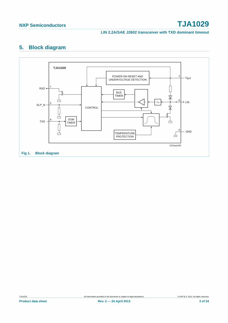
The TJA1029 is the interface between the Local Interconnect Network (LIN) master/slave protocol controller and the physical bus in a LIN network. It is primarily intended for in-vehicle subnetworks using baud rates up to 20 kBd and is compliant with LIN 2.0, LIN 2.1, LIN 2.2, LIN 2.2A and SAE J2602. The TJA1029 is pin-compatible with the TJA1020, TJA1021, TJA1022 and TJA1027.
The protocol controller generates the transmit data stream. The TJA1029 converts the data stream into an optimized bus signal shaped to minimize ElectroMagnetic Emissions (EME). The LIN bus output pin is pulled HIGH via an internal termination resistor. For a master application, connect an external resistor in series with a diode between pin VBAT and pin LIN. The receiver detects a receive data stream on the LIN bus input pin and transfers it via pin RXD to the microcontroller.
Power consumption is very low in Sleep mode. However, the TJA1029 can still be woken up via pins LIN and SLP_N. An integrated TXD dominant time-out function prevents the bus being driven to a permanent dominant state.
2. Features and benefits
2.1 General
Compliant with LIN 2.0, LIN 2.1, LIN 2.2, LIN 2.2A and SAE J2602
Baud rate up to 20 kBd
Very low ElectroMagnetic Emissions (EME)
Very low current consumption in Sleep mode with remote LIN wake-up
Input levels compatible with 3.3 V and 5 V devices
Integrated termination resistor for LIN slave applications
Passive behavior in unpowered state
Operational during cranking pulse: full operation from 5 V upwards
Undervoltage detection
K-line compatible
Available in SO8 and HVSON8 packages
Leadless HVSON8 package (3.0 mm 3.0 mm) with improved Automated Optical Inspection (AOI) capability
Dark green product (halogen free and Restriction of Hazardous Substances (RoHS) compliant)
Pin-compatible subset of the TJA1020, TJA1021 and TJA1022
Pin-compatible with the TJA1027
TJA1029LIN 2.2A/SAE J2602 transceiver with TXD dominant timeoutRev. 2 — 24 April 2013 Product data sheet
NXP Semiconductors TJA1029LIN 2.2A/SAE J2602 transceiver with TXD dominant timeout
2.2 Protection
Very high ElectroMagnetic Immunity (EMI)
Very high ESD robustness: 8 kV according to IEC 61000-4-2 for pins LIN and VBAT
Bus terminal and battery pin protected against transients in the automotive environment (ISO 7637)
Bus terminal short-circuit proof to battery and ground
Thermally protected
Initial TXD dominant check when switching to Normal mode
TXD dominant time-out function
3. Quick reference data
4. Ordering information
Table 1. Quick reference data
Symbol Parameter Conditions Min Typ Max Unit
VBAT battery supply voltage limiting values 0.3 - +42 V
operating range 5 - 18 V
IBAT battery supply current Sleep mode; VLIN = VBAT; VSLP_N = 0 V 2.5 7 10 A
Standby mode; VLIN = VBAT; VSLP_N = 0 V 2.5 7 10 A
Normal mode; VLIN = VBAT; VSLP_N = 5 V; VTXD = 5 V
200 800 1600 A
VLIN voltage on pin LIN limiting value; with respect to GND and VBAT
42 - +42 V
VESD electrostatic discharge voltage on pin LIN; according to IEC 61000-4-2 8 - +8 kV
Tvj virtual junction temperature 40 - +150 C
Table 2. Ordering information
Type number Package
Name Description Version
TJA1029T SO8 plastic small outline package; 8 leads; body width 3.9 mm SOT96-1
TJA1029TK HVSON8 plastic thermal enhanced very thin small outline package; no leads; 8 terminals; body 3 3 0.85 mm
SOT782-1
TJA1029 All information provided in this document is subject to legal disclaimers. © NXP B.V. 2013. All rights reserved.
Product data sheet Rev. 2 — 24 April 2013 2 of 24
NXP Semiconductors TJA1029LIN 2.2A/SAE J2602 transceiver with TXD dominant timeout
5. Block diagram
Fig 1. Block diagram
BUSTIMER
POWER-ON RESET ANDUNDERVOLTAGE DETECTION
VBAT
LIN
GND
015aaa345
6
5TEMPERATUREPROTECTION
CONTROL
TJA1029
SLP_N
TXD
2
4
RXD 1
7
DOMTIMER
TJA1029 All information provided in this document is subject to legal disclaimers. © NXP B.V. 2013. All rights reserved.
Product data sheet Rev. 2 — 24 April 2013 3 of 24
NXP Semiconductors TJA1029LIN 2.2A/SAE J2602 transceiver with TXD dominant timeout
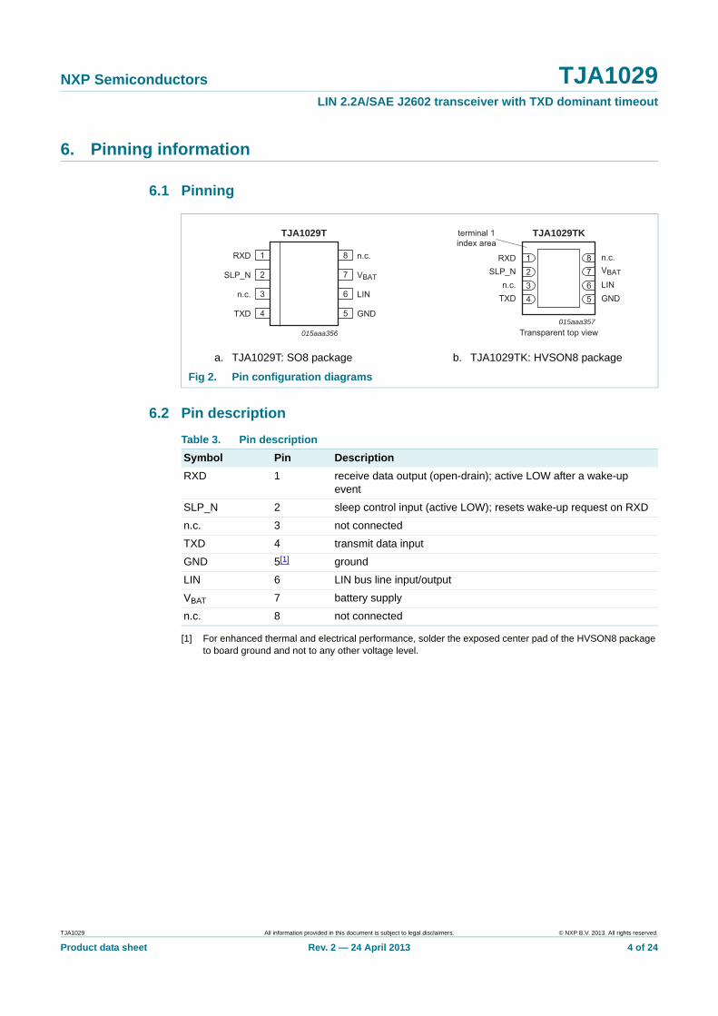
6. Pinning information
6.1 Pinning
6.2 Pin description
[1] For enhanced thermal and electrical performance, solder the exposed center pad of the HVSON8 package to board ground and not to any other voltage level.
a. TJA1029T: SO8 package b. TJA1029TK: HVSON8 package
Fig 2. Pin configuration diagrams
TJA1029T
RXD n.c.
SLP_N VBAT
n.c. LIN
TXD GND
015aaa356
1
2
3
4
6
5
8
7
TXD 4
n.c. 3
SLP_N 2RXD 1
GND5
LIN6
VBAT7
n.c.8
015aaa357
TJA1029TKterminal 1index area
Transparent top view
Table 3. Pin description
Symbol Pin Description
RXD 1 receive data output (open-drain); active LOW after a wake-up event
SLP_N 2 sleep control input (active LOW); resets wake-up request on RXD
n.c. 3 not connected
TXD 4 transmit data input
GND 5[1] ground
LIN 6 LIN bus line input/output
VBAT 7 battery supply
n.c. 8 not connected
TJA1029 All information provided in this document is subject to legal disclaimers. © NXP B.V. 2013. All rights reserved.
Product data sheet Rev. 2 — 24 April 2013 4 of 24
NXP Semiconductors TJA1029LIN 2.2A/SAE J2602 transceiver with TXD dominant timeout
7. Functional description
The TJA1029 is the interface between the LIN master/slave protocol controller and the physical bus in a LIN network. According to the Open System Interconnect (OSI) model, this interface makes up the LIN physical layer.
The LIN transceiver is optimized for, but not limited to, automotive applications with excellent ElectroMagnetic Compatibility (EMC) performance.
7.1 LIN 2.x/SAE J2602 compliant
The TJA1029 is fully LIN 2.0, LIN 2.1, LIN 2.2, LIN 2.2A and SAE J2602 compliant. The LIN physical layer is independent of higher OSI model layers (e.g. the LIN protocol). Consequently, nodes containing a LIN 2.2A-compliant physical layer can be combined, without restriction, with LIN physical layer nodes that comply with earlier revisions (LIN 1.0, LIN 1.1, LIN 1.2, LIN 1.3, LIN 2.0, LIN 2.1 and LIN 2.2).
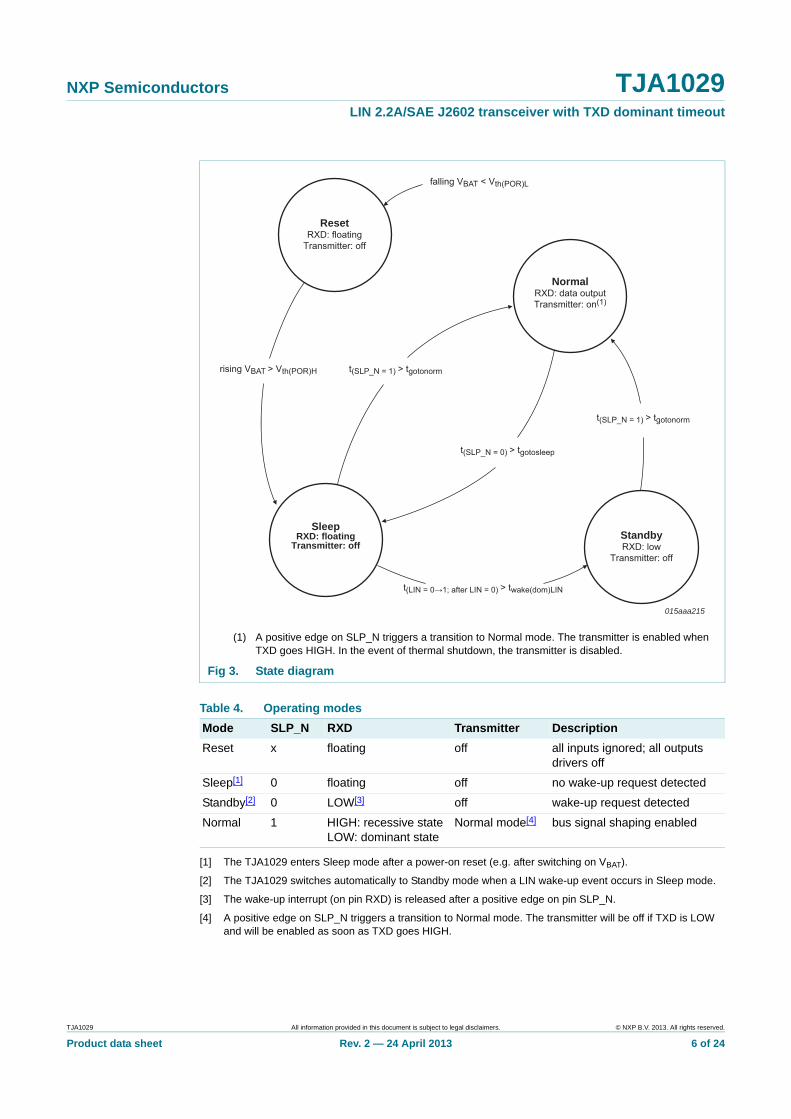
7.2 Operating modes
The TJA1029 supports modes for normal operation (Normal mode) and very-low-power operation (Sleep mode). An intermediate wake-up mode between Sleep and Normal modes is also supported (Standby mode). The state diagram is shown in Figure 3.
TJA1029 All information provided in this document is subject to legal disclaimers. © NXP B.V. 2013. All rights reserved.
Product data sheet Rev. 2 — 24 April 2013 5 of 24
NXP Semiconductors TJA1029LIN 2.2A/SAE J2602 transceiver with TXD dominant timeout
[1] The TJA1029 enters Sleep mode after a power-on reset (e.g. after switching on VBAT).
[2] The TJA1029 switches automatically to Standby mode when a LIN wake-up event occurs in Sleep mode.
[3] The wake-up interrupt (on pin RXD) is released after a positive edge on pin SLP_N.
[4] A positive edge on SLP_N triggers a transition to Normal mode. The transmitter will be off if TXD is LOW and will be enabled as soon as TXD goes HIGH.
(1) A positive edge on SLP_N triggers a transition to Normal mode. The transmitter is enabled when TXD goes HIGH. In the event of thermal shutdown, the transmitter is disabled.
Fig 3. State diagram
Table 4. Operating modes
Mode SLP_N RXD Transmitter Description
Reset x floating off all inputs ignored; all outputs drivers off
Sleep[1] 0 floating off no wake-up request detected
Standby[2] 0 LOW[3] off wake-up request detected
Normal 1 HIGH: recessive state LOW: dominant state
Normal mode[4] bus signal shaping enabled
015aaa215
t(SLP_N = 1) > tgotonorm
t(SLP_N = 1) > tgotonorm
t(SLP_N = 0) > tgotosleep
t(LIN = 0→1; after LIN = 0) > twake(dom)LIN
falling VBAT < Vth(POR)L
NormalRXD: data outputTransmitter: on(1)
StandbyRXD: low
Transmitter: off
SleepRXD: floating
Transmitter: off
ResetRXD: floating
Transmitter: off
rising VBAT > Vth(POR)H
TJA1029 All information provided in this document is subject to legal disclaimers. © NXP B.V. 2013. All rights reserved.
Product data sheet Rev. 2 — 24 April 2013 6 of 24
NXP Semiconductors TJA1029LIN 2.2A/SAE J2602 transceiver with TXD dominant timeout
7.2.1 Reset mode
When the TJA1029 is in Reset mode, it ignores all input signals and all output drivers are off. The TJA1029 switches to Reset mode when the voltage on VBAT drops below the LOW-level power-on reset threshold, Vth(POR)L. When the voltage on VBAT rises above the HIGH-level power-on reset threshold, Vth(POR)H, the TJA1029 switches to Sleep mode.
7.2.2 Sleep mode
The TJA1029 consumes significantly less power in Sleep mode than in Normal mode. Even though current consumption is extremely low in Sleep mode, the TJA1029 can still be woken up remotely via pin LIN or activated directly via pin SLP_N. Filters on the receiver input (LIN) and on pin SLP_N prevent unwanted wake-up events occurring due to automotive transients or radio frequency interference. All wake-up events must be maintained for a specific period (twake(dom)LIN or tgotonorm).
A falling edge on pin SLP_N in Normal mode initiates a transition to Sleep mode. The LIN transmit path is immediately disabled when pin SLP_N goes LOW. In order to ensure the TJA1029 switches successfully to Sleep mode, the sleep command (pin SLP_N = LOW) must be maintained for at least tgotosleep.
Sleep mode activation is independent of the levels on pins LIN or TXD. So the lowest possible power consumption can be guaranteed, even when there is a continuous dominant level on pins LIN and TXD.
7.2.3 Standby mode
Standby mode is activated automatically when a local or remote wake-up event occurs while the TJA1029 is in Sleep mode. In Standby mode, pin RXD is held LOW to provide an interrupt flag for the microcontroller.
7.2.4 Normal mode
In Normal mode, the TJA1029 can transmit and receive data via the LIN bus.
The receiver detects the data stream on the LIN bus input pin and transfers it via pin RXD to the microcontroller (see Figure 6): HIGH for a recessive level and LOW for a dominant level on the bus. The receiver has a supply-voltage related threshold with hysteresis and an integrated filter to suppress bus line noise.
The transmitter converts the transmit data stream from the protocol controller, detected on pin TXD, into an optimized bus signal. The optimized bus signal is shaped to minimize EME. The LIN bus output pin is pulled HIGH via an internal slave termination resistor. For a master application, connect an external resistor in series with a diode between pin VBAT and pin LIN (see Figure 6).
If pin SLP_N is pulled HIGH while the TJA1029 is in Sleep or Standby mode, the LIN transceiver switches to Normal mode after tgotonorm.
TJA1029 All information provided in this document is subject to legal disclaimers. © NXP B.V. 2013. All rights reserved.
Product data sheet Rev. 2 — 24 April 2013 7 of 24
NXP Semiconductors TJA1029LIN 2.2A/SAE J2602 transceiver with TXD dominant timeout
7.3 Transceiver wake-up
7.3.1 Remote wake-up via the LIN bus
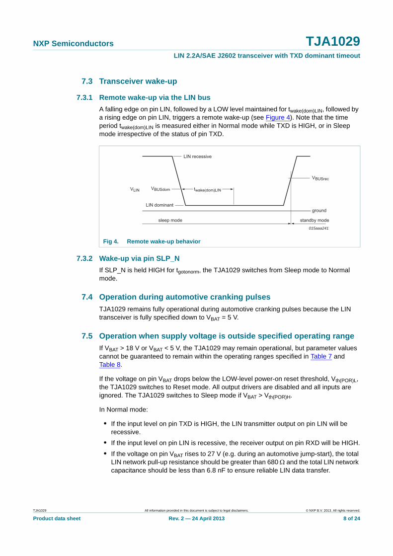
A falling edge on pin LIN, followed by a LOW level maintained for twake(dom)LIN, followed by a rising edge on pin LIN, triggers a remote wake-up (see Figure 4). Note that the time period twake(dom)LIN is measured either in Normal mode while TXD is HIGH, or in Sleep mode irrespective of the status of pin TXD.
7.3.2 Wake-up via pin SLP_N
If SLP_N is held HIGH for tgotonorm, the TJA1029 switches from Sleep mode to Normal mode.
7.4 Operation during automotive cranking pulses
TJA1029 remains fully operational during automotive cranking pulses because the LIN transceiver is fully specified down to VBAT = 5 V.
7.5 Operation when supply voltage is outside specified operating range
If VBAT > 18 V or VBAT < 5 V, the TJA1029 may remain operational, but parameter values cannot be guaranteed to remain within the operating ranges specified in Table 7 and Table 8.
If the voltage on pin VBAT drops below the LOW-level power-on reset threshold, Vth(POR)L, the TJA1029 switches to Reset mode. All output drivers are disabled and all inputs are ignored. The TJA1029 switches to Sleep mode if VBAT > Vth(POR)H.
In Normal mode:
• If the input level on pin TXD is HIGH, the LIN transmitter output on pin LIN will be recessive.
• If the input level on pin LIN is recessive, the receiver output on pin RXD will be HIGH.
• If the voltage on pin VBAT rises to 27 V (e.g. during an automotive jump-start), the total LIN network pull-up resistance should be greater than 680 and the total LIN network capacitance should be less than 6.8 nF to ensure reliable LIN data transfer.
Fig 4. Remote wake-up behavior
015aaa241
LIN recessive
LIN dominant
sleep mode standby mode
VBUSdom
VBUSrec
ground
VLIN twake(dom)LIN
TJA1029 All information provided in this document is subject to legal disclaimers. © NXP B.V. 2013. All rights reserved.
Product data sheet Rev. 2 — 24 April 2013 8 of 24
NXP Semiconductors TJA1029LIN 2.2A/SAE J2602 transceiver with TXD dominant timeout
• If the voltage on pin VBAT drops below the LOW-level VBAT LOW threshold, Vth(VBATL)L, the LIN transmit path is interrupted and the LIN output remains recessive. The LIN transmit path is switched on again when VBAT rises above Vth(VBATL)H and the input to pin TXD is recessive.
7.6 TXD dominant time-out function
An initial TXD dominant check prevents the bus line being driven to a permanent dominant state (blocking all network communications) if pin TXD is forced permanently LOW by a hardware and/or software application failure. The TXD input level is checked after a transition to Normal mode. If TXD is LOW, the transmit path remains disabled and is only enabled when TXD goes HIGH.
Once the transmitter has been enabled, a TXD dominant time-out timer is started every time pin TXD goes LOW. If the LOW state on pin TXD persists for longer than the TXD dominant time-out time (tto(dom)TXD), the transmitter is disabled, releasing the bus line to recessive state. The TXD dominant time-out timer is reset when pin TXD goes HIGH.
7.7 Fail-safe features
A pull-down to GND on pin TXD forces a predefined level on the transmit data input if the pin is disconnected.
A pull-down to GND on pin SLP_N forces the transceiver into Sleep mode if pin SLP_N is disconnected.
Pin RXD is set floating if VBAT is disconnected.
The current in the transmitter output stage is limited in order to protect the transmitter against short circuits to pins VBAT or GND.
A loss of power (pins VBAT and GND) has no impact on the bus line or on the microcontroller. No reverse currents flow from the bus into pin LIN. The current path from VBAT to LIN via the integrated LIN slave termination resistor remains. The LIN transceiver can be disconnected from the power supply without influencing the LIN bus.
The output driver on pin LIN is protected against overtemperature conditions. If the junction temperature exceeds the shutdown junction temperature, Tj(sd), the thermal protection circuit disables the output driver. The driver is enabled again when the junction temperature falls below Tj(sd) and pin TXD is recessive.
TJA1029 All information provided in this document is subject to legal disclaimers. © NXP B.V. 2013. All rights reserved.
Product data sheet Rev. 2 — 24 April 2013 9 of 24
NXP Semiconductors TJA1029LIN 2.2A/SAE J2602 transceiver with TXD dominant timeout
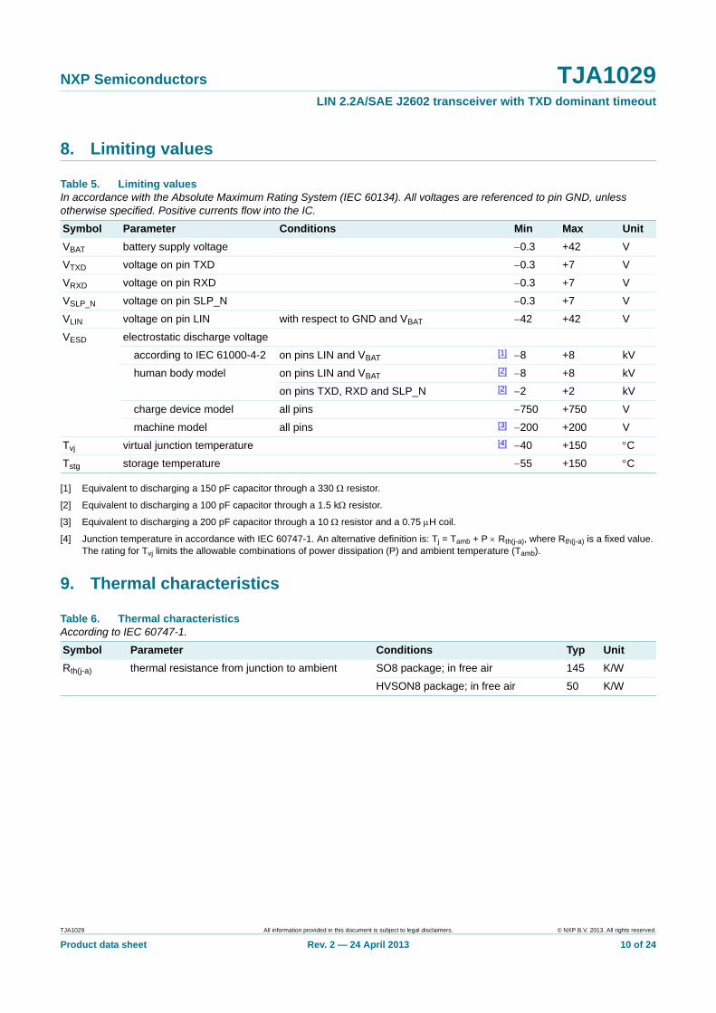
8. Limiting values
[1] Equivalent to discharging a 150 pF capacitor through a 330 resistor.
[2] Equivalent to discharging a 100 pF capacitor through a 1.5 k resistor.
[3] Equivalent to discharging a 200 pF capacitor through a 10 resistor and a 0.75 H coil.
[4] Junction temperature in accordance with IEC 60747-1. An alternative definition is: Tj = Tamb + P Rth(j-a), where Rth(j-a) is a fixed value. The rating for Tvj limits the allowable combinations of power dissipation (P) and ambient temperature (Tamb).
9. Thermal characteristics
Table 5. Limiting valuesIn accordance with the Absolute Maximum Rating System (IEC 60134). All voltages are referenced to pin GND, unless otherwise specified. Positive currents flow into the IC.
Symbol Parameter Conditions Min Max Unit
VBAT battery supply voltage 0.3 +42 V
VTXD voltage on pin TXD 0.3 +7 V
VRXD voltage on pin RXD 0.3 +7 V
VSLP_N voltage on pin SLP_N 0.3 +7 V
VLIN voltage on pin LIN with respect to GND and VBAT 42 +42 V
VESD electrostatic discharge voltage
according to IEC 61000-4-2 on pins LIN and VBAT [1] 8 +8 kV
human body model on pins LIN and VBAT [2] 8 +8 kV
on pins TXD, RXD and SLP_N [2] 2 +2 kV
charge device model all pins 750 +750 V
machine model all pins [3] 200 +200 V
Tvj virtual junction temperature [4] 40 +150 C
Tstg storage temperature 55 +150 C
Table 6. Thermal characteristicsAccording to IEC 60747-1.
Symbol Parameter Conditions Typ Unit
Rth(j-a) thermal resistance from junction to ambient SO8 package; in free air 145 K/W
HVSON8 package; in free air 50 K/W
TJA1029 All information provided in this document is subject to legal disclaimers. © NXP B.V. 2013. All rights reserved.
Product data sheet Rev. 2 — 24 April 2013 10 of 24
NXP Semiconductors TJA1029LIN 2.2A/SAE J2602 transceiver with TXD dominant timeout
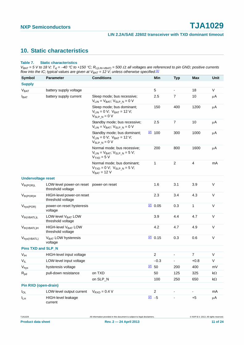
10. Static characteristics
Table 7. Static characteristicsVBAT = 5 V to 18 V; Tvj = 40 C to +150 C; RL(LIN-VBAT) = 500 ; all voltages are referenced to pin GND; positive currents flow into the IC; typical values are given at VBAT = 12 V; unless otherwise specified.[1]
Symbol Parameter Conditions Min Typ Max Unit
Supply
VBAT battery supply voltage 5 - 18 V
IBAT battery supply current Sleep mode; bus recessive;VLIN = VBAT; VSLP_N = 0 V
2.5 7 10 A
Sleep mode; bus dominant;VLIN = 0 V; VBAT = 12 V; VSLP_N = 0 V
150 400 1200 A
Standby mode; bus recessive;VLIN = VBAT; VSLP_N = 0 V
2.5 7 10 A
Standby mode; bus dominant;VLIN = 0 V; VBAT = 12 V; VSLP_N = 0 V
[2] 100 300 1000 A
Normal mode; bus recessive;VLIN = VBAT; VSLP_N = 5 V; VTXD = 5 V
200 800 1600 A
Normal mode; bus dominant;VTXD = 0 V; VSLP_N = 5 V;VBAT = 12 V
1 2 4 mA
Undervoltage reset
Vth(POR)L LOW-level power-on reset threshold voltage
power-on reset 1.6 3.1 3.9 V
Vth(POR)H HIGH-level power-on reset threshold voltage
2.3 3.4 4.3 V
Vhys(POR) power-on reset hysteresis voltage
[2] 0.05 0.3 1 V
Vth(VBATL)L LOW-level VBAT LOW threshold voltage
3.9 4.4 4.7 V
Vth(VBATL)H HIGH-level VBAT LOW threshold voltage
4.2 4.7 4.9 V
Vhys(VBATL) VBAT LOW hysteresis voltage
[2] 0.15 0.3 0.6 V
Pins TXD and SLP_N
VIH HIGH-level input voltage 2 - 7 V
VIL LOW-level input voltage 0.3 - +0.8 V
Vhys hysteresis voltage [2] 50 200 400 mV
Rpd pull-down resistance on TXD 50 125 325 k
on SLP_N 100 250 650 k
Pin RXD (open-drain)
IOL LOW-level output current VRXD = 0.4 V 2 - - mA
ILH HIGH-level leakage current
[2] 5 - +5 A
TJA1029 All information provided in this document is subject to legal disclaimers. © NXP B.V. 2013. All rights reserved.
Product data sheet Rev. 2 — 24 April 2013 11 of 24
NXP Semiconductors TJA1029LIN 2.2A/SAE J2602 transceiver with TXD dominant timeout
[1] All parameters are guaranteed over the virtual junction temperature range by design. Factory testing uses correlated test conditions to cover the specified temperature and power supply voltage range.
[2] Not tested in production; guaranteed by design.
Pin LIN
IBUS_LIM current limitation for driver dominant state
VBAT = 18 V; VLIN = 18 V; VTXD = 0 V
40 - 100 mA
IBUS_PAS_dom receiver dominant input leakage current including pull-up resistor
VBAT = 12 V; VLIN = 0 V;VTXD = 5 V
[2] 600 - - A
IBUS_PAS_rec receiver recessive input leakage current
VBAT = 5 V; VLIN = 18 V;VTXD = 5 V
[2] - 0 1 A
IBUS_NO_GND loss-of-ground bus current VBAT = 18 V; VLIN = 0 V [2] 750 - +10 A
IBUS_NO_BAT loss-of-battery bus current VBAT = 0 V; VLIN = 18 V [2] - - 1 A
VBUSdom receiver dominant state - - 0.4VBAT V
VBUSrec receiver recessive state 0.6VBAT - - V
VBUS_CNT receiver center voltage VBUS_CNT =(VBUSdom + VBUSrec) / 2
0.475VBAT 0.5VBAT 0.525VBAT V
VHYS receiver hysteresis voltage VHYS = VBUSrec VBUSdom - - 0.175VBAT V
VSerDiode voltage drop at the serial diode
in pull-up path with Rslave; ISerDiode = 0.9 mA
[2] 0.4 - 1.0 V
VO(dom) dominant output voltage Normal mode; VTXD = 0 V;VBAT = 7.0 V
[2] - - 1.4 V
Normal mode; VTXD = 0 V;VBAT = 18 V
[2] - - 2.0 V
Rslave slave resistance 20 30 60 k
CLIN capacitance on pin LIN with respect to GND [2] - - 20 pF
Thermal shutdown
Tj(sd) shutdown junction temperature
[2] 150 - 200 C
Table 7. Static characteristics …continuedVBAT = 5 V to 18 V; Tvj = 40 C to +150 C; RL(LIN-VBAT) = 500 ; all voltages are referenced to pin GND; positive currents flow into the IC; typical values are given at VBAT = 12 V; unless otherwise specified.[1]
Symbol Parameter Conditions Min Typ Max Unit
TJA1029 All information provided in this document is subject to legal disclaimers. © NXP B.V. 2013. All rights reserved.
Product data sheet Rev. 2 — 24 April 2013 12 of 24
NXP Semiconductors TJA1029LIN 2.2A/SAE J2602 transceiver with TXD dominant timeout
11. Dynamic characteristics
[1] All parameters are guaranteed over the virtual junction temperature range by design. Factory testing uses correlated test conditions to cover the specified temperature and power supply voltage ranges.
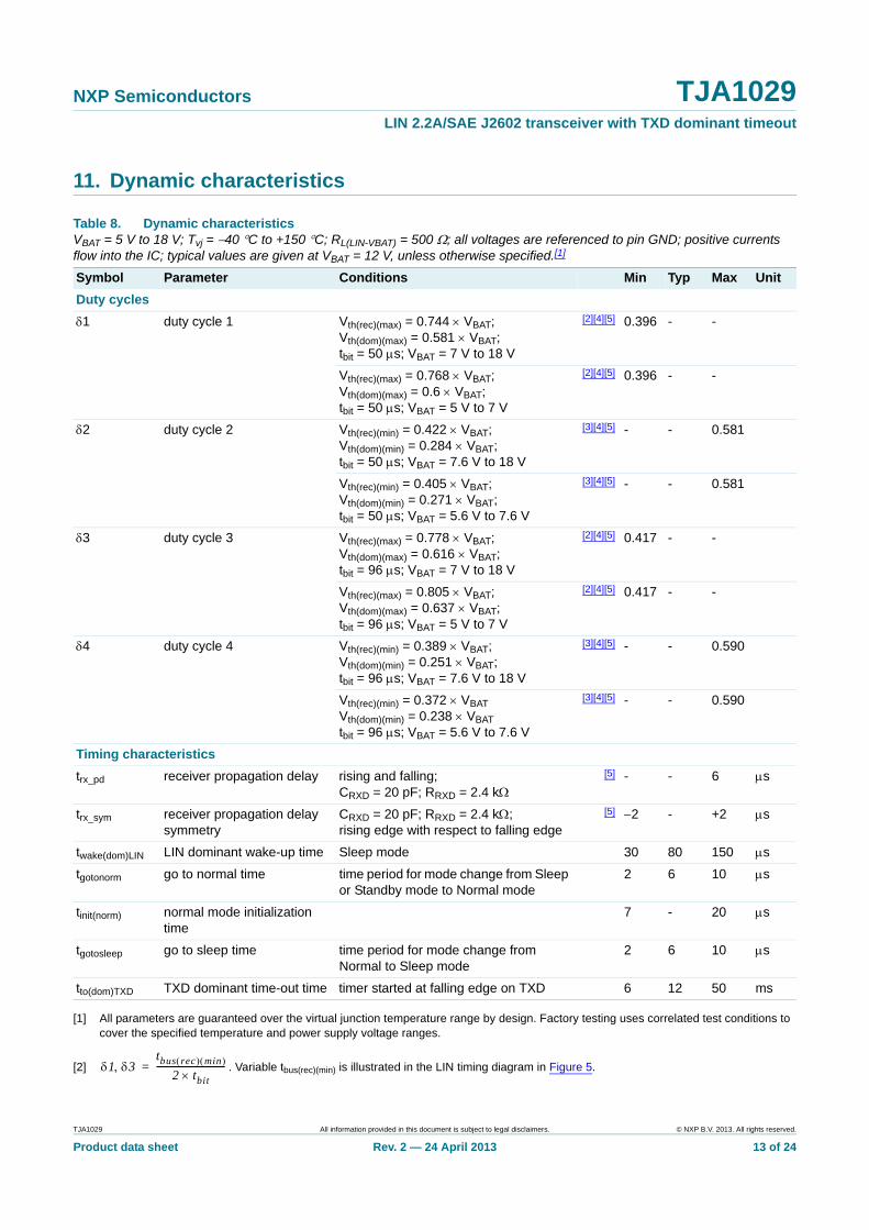
[2] . Variable tbus(rec)(min) is illustrated in the LIN timing diagram in Figure 5.
Table 8. Dynamic characteristicsVBAT = 5 V to 18 V; Tvj = 40 C to +150 C; RL(LIN-VBAT) = 500 ; all voltages are referenced to pin GND; positive currents flow into the IC; typical values are given at VBAT = 12 V, unless otherwise specified.[1]
Symbol Parameter Conditions Min Typ Max Unit
Duty cycles
1 duty cycle 1 Vth(rec)(max) = 0.744 VBAT; Vth(dom)(max) = 0.581 VBAT;tbit = 50 s; VBAT = 7 V to 18 V
[2][4][5] 0.396 - -
Vth(rec)(max) = 0.768 VBAT; Vth(dom)(max) = 0.6 VBAT;tbit = 50 s; VBAT = 5 V to 7 V
[2][4][5] 0.396 - -
2 duty cycle 2 Vth(rec)(min) = 0.422 VBAT;Vth(dom)(min) = 0.284 VBAT;tbit = 50 s; VBAT = 7.6 V to 18 V
[3][4][5] - - 0.581
Vth(rec)(min) = 0.405 VBAT;Vth(dom)(min) = 0.271 VBAT;tbit = 50 s; VBAT = 5.6 V to 7.6 V
[3][4][5] - - 0.581
3 duty cycle 3 Vth(rec)(max) = 0.778 VBAT;Vth(dom)(max) = 0.616 VBAT;tbit = 96 s; VBAT = 7 V to 18 V
[2][4][5] 0.417 - -
Vth(rec)(max) = 0.805 VBAT;Vth(dom)(max) = 0.637 VBAT;tbit = 96 s; VBAT = 5 V to 7 V
[2][4][5] 0.417 - -
4 duty cycle 4 Vth(rec)(min) = 0.389 VBAT;Vth(dom)(min) = 0.251 VBAT;tbit = 96 s; VBAT = 7.6 V to 18 V
[3][4][5] - - 0.590
Vth(rec)(min) = 0.372 VBATVth(dom)(min) = 0.238 VBATtbit = 96 s; VBAT = 5.6 V to 7.6 V
[3][4][5] - - 0.590
Timing characteristics
trx_pd receiver propagation delay rising and falling;CRXD = 20 pF; RRXD = 2.4 k
[5] - - 6 s
trx_sym receiver propagation delay symmetry
CRXD = 20 pF; RRXD = 2.4 k;rising edge with respect to falling edge
[5] 2 - +2 s
twake(dom)LIN LIN dominant wake-up time Sleep mode 30 80 150 s
tgotonorm go to normal time time period for mode change from Sleep or Standby mode to Normal mode
2 6 10 s
tinit(norm) normal mode initialization time
7 - 20 s
tgotosleep go to sleep time time period for mode change from Normal to Sleep mode
2 6 10 s
tto(dom)TXD TXD dominant time-out time timer started at falling edge on TXD 6 12 50 ms
1 3tbus rec min
2 tbit-------------------------------=
TJA1029 All information provided in this document is subject to legal disclaimers. © NXP B.V. 2013. All rights reserved.
Product data sheet Rev. 2 — 24 April 2013 13 of 24
NXP Semiconductors TJA1029LIN 2.2A/SAE J2602 transceiver with TXD dominant timeout
[3] . Variable tbus(rec)(max) is illustrated in the LIN timing diagram in Figure 5.
[4] Bus load conditions: CBUS = 1 nF and RBUS = 1 k; CBUS = 6.8 nF and RBUS = 660 ; CBUS = 10 nF and RBUS = 500 .
[5] See timing diagram in Figure 5.
2 4tbus rec max
2 tbit--------------------------------=
Fig 5. Timing diagram of LIN transceiver duty cycle
VTXD
tbit tbit
Vth(rec)(max)
Vth(dom)(max)
Vth(rec)(min)
Vth(dom)(min)
thresholds ofreceiving node 1
thresholds ofreceiving node 2
LIN BUSsignalVBAT
receivingnode 1
receivingnode 2
VRXD
VRXD
trx_pdf
015aaa237
trx_pdf
trx_pdr trx_pdf
trx_pdftrx_pdr
tbus(rec)(min)tbus(dom)(max)
tbus(rec)(max)tbus(dom)(min)
TJA1029 All information provided in this document is subject to legal disclaimers. © NXP B.V. 2013. All rights reserved.
Product data sheet Rev. 2 — 24 April 2013 14 of 24
NXP Semiconductors TJA1029LIN 2.2A/SAE J2602 transceiver with TXD dominant timeout
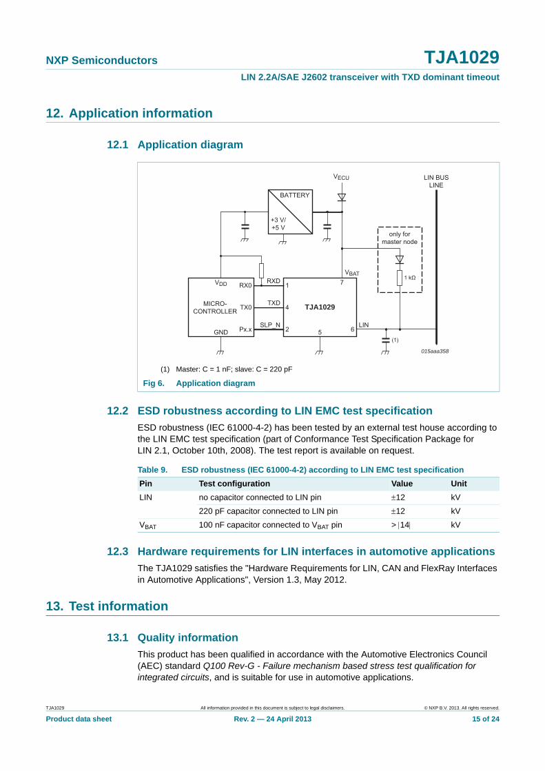
12. Application information
12.1 Application diagram
12.2 ESD robustness according to LIN EMC test specification
ESD robustness (IEC 61000-4-2) has been tested by an external test house according to the LIN EMC test specification (part of Conformance Test Specification Package for LIN 2.1, October 10th, 2008). The test report is available on request.
12.3 Hardware requirements for LIN interfaces in automotive applications
The TJA1029 satisfies the "Hardware Requirements for LIN, CAN and FlexRay Interfaces in Automotive Applications", Version 1.3, May 2012.
13. Test information
13.1 Quality information
This product has been qualified in accordance with the Automotive Electronics Council (AEC) standard Q100 Rev-G - Failure mechanism based stress test qualification for integrated circuits, and is suitable for use in automotive applications.
(1) Master: C = 1 nF; slave: C = 220 pF
Fig 6. Application diagram
015aaa358
1 kΩVBAT
LIN BUSLINE
only formaster node
LIN
(1)
7
5
1
4
2 6
TJA1029
VDD
GND
TX0
Px.x
RX0
TXD
SLP_N
RXD
MICRO-CONTROLLER
BATTERY
+3 V/+5 V
VECU
Table 9. ESD robustness (IEC 61000-4-2) according to LIN EMC test specification
Pin Test configuration Value Unit
LIN no capacitor connected to LIN pin 12 kV
220 pF capacitor connected to LIN pin 12 kV
VBAT 100 nF capacitor connected to VBAT pin > 14 kV
TJA1029 All information provided in this document is subject to legal disclaimers. © NXP B.V. 2013. All rights reserved.
Product data sheet Rev. 2 — 24 April 2013 15 of 24
NXP Semiconductors TJA1029LIN 2.2A/SAE J2602 transceiver with TXD dominant timeout
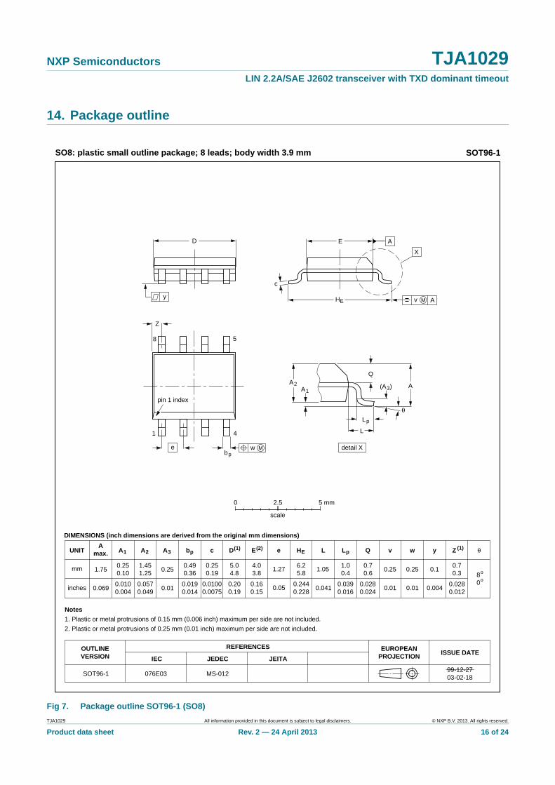
14. Package outline
Fig 7. Package outline SOT96-1 (SO8)
UNITA
max. A1 A2 A3 bp c D(1) E(2) (1)e HE L Lp Q Zywv θ
REFERENCESOUTLINEVERSION
EUROPEANPROJECTION ISSUE DATE
IEC JEDEC JEITA
mm
inches
1.750.250.10
1.451.25
0.250.490.36
0.250.19
5.04.8
4.03.8
1.276.25.8
1.050.70.6
0.70.3 8
0
o
o
0.25 0.10.25
DIMENSIONS (inch dimensions are derived from the original mm dimensions)
Notes
1. Plastic or metal protrusions of 0.15 mm (0.006 inch) maximum per side are not included.
2. Plastic or metal protrusions of 0.25 mm (0.01 inch) maximum per side are not included.
1.00.4
SOT96-1
X
w M
θ
AA1
A2
bp
D
HE
Lp
Q
detail X
E
Z
e
c
L
v M A
(A )3
A
4
5
pin 1 index
1
8
y
076E03 MS-012
0.0690.0100.004
0.0570.049
0.010.0190.014
0.01000.0075
0.200.19
0.160.15
0.050.2440.228
0.0280.024
0.0280.012
0.010.010.041 0.0040.0390.016
0 2.5 5 mm
scale
SO8: plastic small outline package; 8 leads; body width 3.9 mm SOT96-1
99-12-2703-02-18
TJA1029 All information provided in this document is subject to legal disclaimers. © NXP B.V. 2013. All rights reserved.
Product data sheet Rev. 2 — 24 April 2013 16 of 24
NXP Semiconductors TJA1029LIN 2.2A/SAE J2602 transceiver with TXD dominant timeout
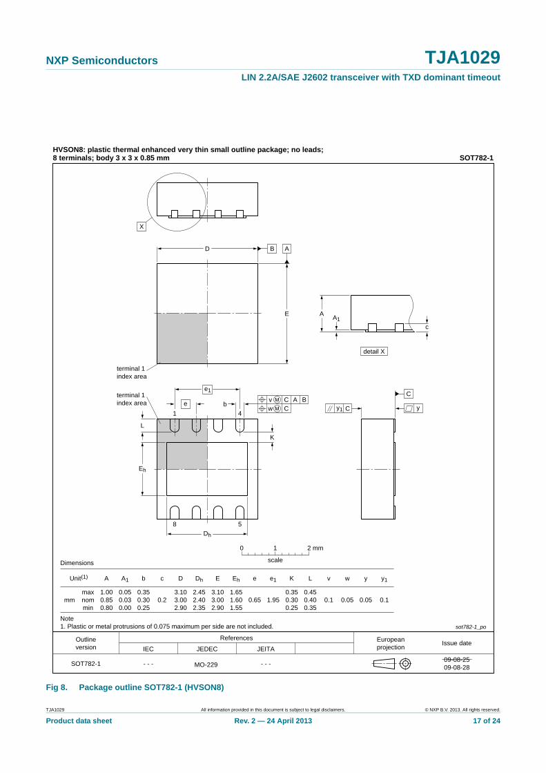
Fig 8. Package outline SOT782-1 (HVSON8)
ReferencesOutlineversion
Europeanprojection
Issue dateIEC JEDEC JEITA
SOT782-1 - - -- - -
sot782-1_po
09-08-2509-08-28
Unit(1)
mmmaxnommin
1.000.850.80
0.050.030.00
0.23.103.002.90
2.452.402.35
3.103.002.90
0.65 1.950.450.400.35
0.1
A
Dimensions
Note1. Plastic or metal protrusions of 0.075 maximum per side are not included.
HVSON8: plastic thermal enhanced very thin small outline package; no leads;8 terminals; body 3 x 3 x 0.85 mm SOT782-1
A1 b
0.350.300.25
c D Dh E Eh
1.651.601.55
e e1 K
0.350.300.25
L v
0.1
w
0.05
y
0.05
y1
0 1 2 mm
scale
MO-229
X
C
yCy1
detail X
A
cA1
B AD
E
terminal 1index area
b
Dh
L
Eh
K
e1
eAC Bv
Cw1 4
8 5
terminal 1index area
TJA1029 All information provided in this document is subject to legal disclaimers. © NXP B.V. 2013. All rights reserved.
Product data sheet Rev. 2 — 24 April 2013 17 of 24
NXP Semiconductors TJA1029LIN 2.2A/SAE J2602 transceiver with TXD dominant timeout
15. Handling information
All input and output pins are protected against ElectroStatic Discharge (ESD) under normal handling. When handling ensure that the appropriate precautions are taken as described in JESD625-A or equivalent standards.
16. Soldering of SMD packages
This text provides a very brief insight into a complex technology. A more in-depth account of soldering ICs can be found in Application Note AN10365 “Surface mount reflow soldering description”.
16.1 Introduction to soldering
Soldering is one of the most common methods through which packages are attached to Printed Circuit Boards (PCBs), to form electrical circuits. The soldered joint provides both the mechanical and the electrical connection. There is no single soldering method that is ideal for all IC packages. Wave soldering is often preferred when through-hole and Surface Mount Devices (SMDs) are mixed on one printed wiring board; however, it is not suitable for fine pitch SMDs. Reflow soldering is ideal for the small pitches and high densities that come with increased miniaturization.
16.2 Wave and reflow soldering
Wave soldering is a joining technology in which the joints are made by solder coming from a standing wave of liquid solder. The wave soldering process is suitable for the following:
• Through-hole components
• Leaded or leadless SMDs, which are glued to the surface of the printed circuit board
Not all SMDs can be wave soldered. Packages with solder balls, and some leadless packages which have solder lands underneath the body, cannot be wave soldered. Also, leaded SMDs with leads having a pitch smaller than ~0.6 mm cannot be wave soldered, due to an increased probability of bridging.
The reflow soldering process involves applying solder paste to a board, followed by component placement and exposure to a temperature profile. Leaded packages, packages with solder balls, and leadless packages are all reflow solderable.
Key characteristics in both wave and reflow soldering are:
• Board specifications, including the board finish, solder masks and vias
• Package footprints, including solder thieves and orientation
• The moisture sensitivity level of the packages
• Package placement
• Inspection and repair
• Lead-free soldering versus SnPb soldering
16.3 Wave soldering
Key characteristics in wave soldering are:
TJA1029 All information provided in this document is subject to legal disclaimers. © NXP B.V. 2013. All rights reserved.
Product data sheet Rev. 2 — 24 April 2013 18 of 24
NXP Semiconductors TJA1029LIN 2.2A/SAE J2602 transceiver with TXD dominant timeout
• Process issues, such as application of adhesive and flux, clinching of leads, board transport, the solder wave parameters, and the time during which components are exposed to the wave
• Solder bath specifications, including temperature and impurities
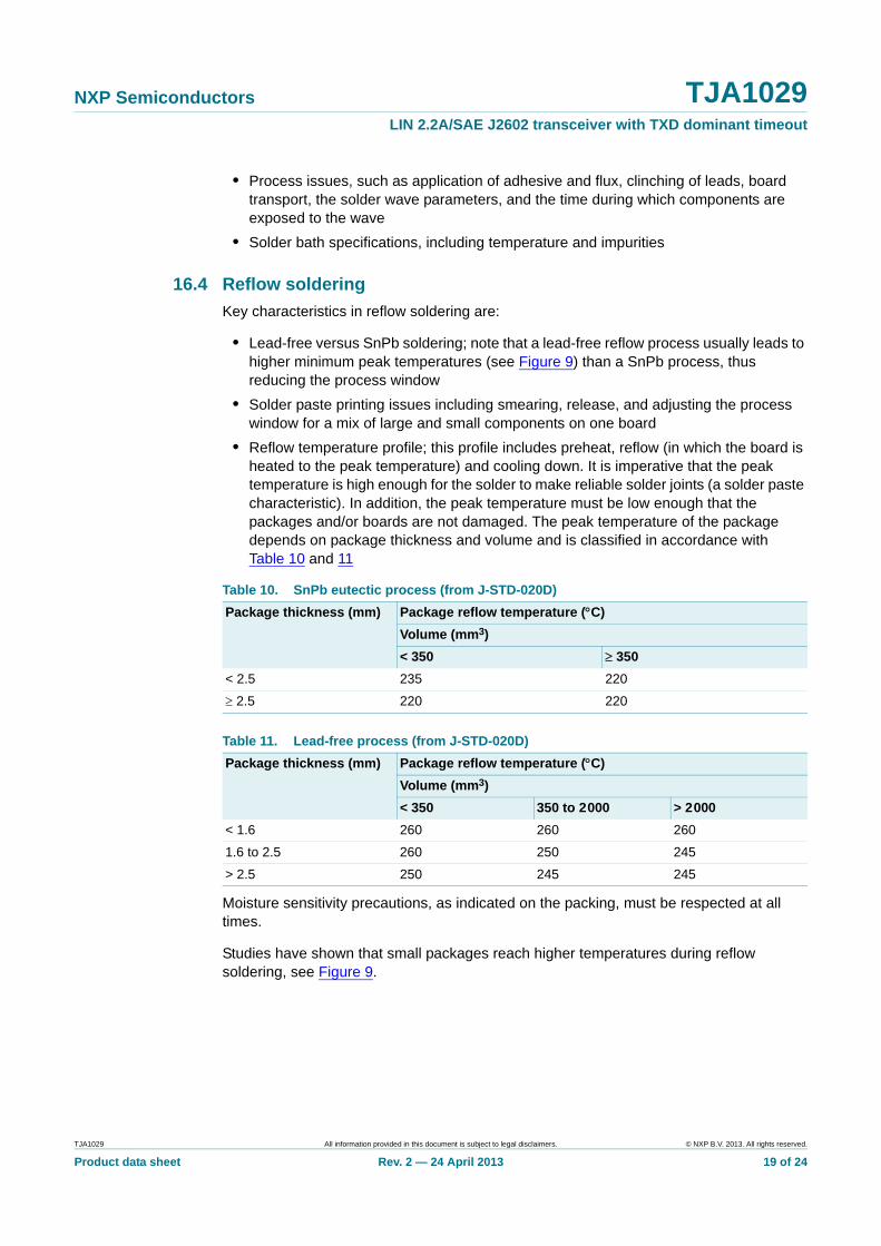
16.4 Reflow soldering
Key characteristics in reflow soldering are:
• Lead-free versus SnPb soldering; note that a lead-free reflow process usually leads to higher minimum peak temperatures (see Figure 9) than a SnPb process, thus reducing the process window
• Solder paste printing issues including smearing, release, and adjusting the process window for a mix of large and small components on one board
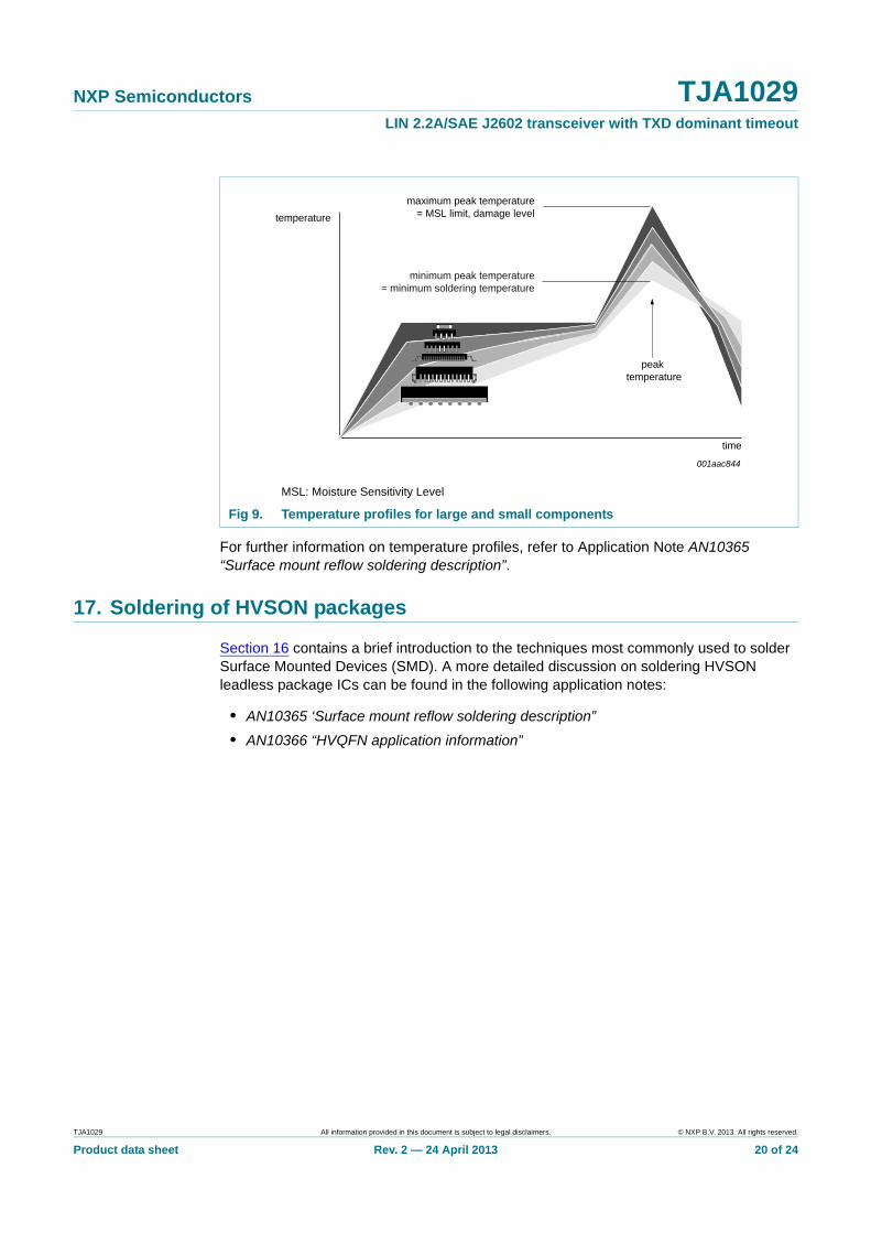
• Reflow temperature profile; this profile includes preheat, reflow (in which the board is heated to the peak temperature) and cooling down. It is imperative that the peak temperature is high enough for the solder to make reliable solder joints (a solder paste characteristic). In addition, the peak temperature must be low enough that the packages and/or boards are not damaged. The peak temperature of the package depends on package thickness and volume and is classified in accordance with Table 10 and 11
Moisture sensitivity precautions, as indicated on the packing, must be respected at all times.
Studies have shown that small packages reach higher temperatures during reflow soldering, see Figure 9.
Table 10. SnPb eutectic process (from J-STD-020D)
Package thickness (mm) Package reflow temperature (C)
Volume (mm3)
< 350 350
< 2.5 235 220
2.5 220 220
Table 11. Lead-free process (from J-STD-020D)
Package thickness (mm) Package reflow temperature (C)
Volume (mm3)
< 350 350 to 2000 > 2000
< 1.6 260 260 260
1.6 to 2.5 260 250 245
> 2.5 250 245 245
TJA1029 All information provided in this document is subject to legal disclaimers. © NXP B.V. 2013. All rights reserved.
Product data sheet Rev. 2 — 24 April 2013 19 of 24
NXP Semiconductors TJA1029LIN 2.2A/SAE J2602 transceiver with TXD dominant timeout
For further information on temperature profiles, refer to Application Note AN10365 “Surface mount reflow soldering description”.
17. Soldering of HVSON packages
Section 16 contains a brief introduction to the techniques most commonly used to solder Surface Mounted Devices (SMD). A more detailed discussion on soldering HVSON leadless package ICs can be found in the following application notes:
• AN10365 ‘Surface mount reflow soldering description”
• AN10366 “HVQFN application information”
MSL: Moisture Sensitivity Level
Fig 9. Temperature profiles for large and small components
001aac844
temperature
time
minimum peak temperature= minimum soldering temperature
maximum peak temperature= MSL limit, damage level
peak temperature
TJA1029 All information provided in this document is subject to legal disclaimers. © NXP B.V. 2013. All rights reserved.
Product data sheet Rev. 2 — 24 April 2013 20 of 24
NXP Semiconductors TJA1029LIN 2.2A/SAE J2602 transceiver with TXD dominant timeout
18. Revision history
Table 12. Revision history
Document ID Release date Data sheet status Change notice Supersedes
TJA1029 v.2 20130424 Product data sheet - TJA1029 v.1
Modifications: • Table 7: revised measurement conditions for parameter IBUS_NO_BAT
• Section 13.1 text revised
TJA1029 v.1 20130108 Product data sheet - -
TJA1029 All information provided in this document is subject to legal disclaimers. © NXP B.V. 2013. All rights reserved.
Product data sheet Rev. 2 — 24 April 2013 21 of 24
NXP Semiconductors TJA1029LIN 2.2A/SAE J2602 transceiver with TXD dominant timeout
19. Legal information
19.1 Data sheet status
[1] Please consult the most recently issued document before initiating or completing a design.
[2] The term ‘short data sheet’ is explained in section “Definitions”.
[3] The product status of device(s) described in this document may have changed since this document was published and may differ in case of multiple devices. The latest product status information is available on the Internet at URL http://www.nxp.com.
19.2 Definitions
Draft — The document is a draft version only. The content is still under internal review and subject to formal approval, which may result in modifications or additions. NXP Semiconductors does not give any representations or warranties as to the accuracy or completeness of information included herein and shall have no liability for the consequences of use of such information.
Short data sheet — A short data sheet is an extract from a full data sheet with the same product type number(s) and title. A short data sheet is intended for quick reference only and should not be relied upon to contain detailed and full information. For detailed and full information see the relevant full data sheet, which is available on request via the local NXP Semiconductors sales office. In case of any inconsistency or conflict with the short data sheet, the full data sheet shall prevail.
Product specification — The information and data provided in a Product data sheet shall define the specification of the product as agreed between NXP Semiconductors and its customer, unless NXP Semiconductors and customer have explicitly agreed otherwise in writing. In no event however, shall an agreement be valid in which the NXP Semiconductors product is deemed to offer functions and qualities beyond those described in the Product data sheet.
19.3 Disclaimers
Limited warranty and liability — Information in this document is believed to be accurate and reliable. However, NXP Semiconductors does not give any representations or warranties, expressed or implied, as to the accuracy or completeness of such information and shall have no liability for the consequences of use of such information. NXP Semiconductors takes no responsibility for the content in this document if provided by an information source outside of NXP Semiconductors.
In no event shall NXP Semiconductors be liable for any indirect, incidental, punitive, special or consequential damages (including - without limitation - lost profits, lost savings, business interruption, costs related to the removal or replacement of any products or rework charges) whether or not such damages are based on tort (including negligence), warranty, breach of contract or any other legal theory.
Notwithstanding any damages that customer might incur for any reason whatsoever, NXP Semiconductors’ aggregate and cumulative liability towards customer for the products described herein shall be limited in accordance with the Terms and conditions of commercial sale of NXP Semiconductors.
Right to make changes — NXP Semiconductors reserves the right to make changes to information published in this document, including without limitation specifications and product descriptions, at any time and without notice. This document supersedes and replaces all information supplied prior to the publication hereof.
Suitability for use in automotive applications — This NXP Semiconductors product has been qualified for use in automotive applications. Unless otherwise agreed in writing, the product is not designed, authorized or warranted to be suitable for use in life support, life-critical or safety-critical systems or equipment, nor in applications where failure or malfunction of an NXP Semiconductors product can reasonably be expected to result in personal injury, death or severe property or environmental damage. NXP Semiconductors and its suppliers accept no liability for inclusion and/or use of NXP Semiconductors products in such equipment or applications and therefore such inclusion and/or use is at the customer's own risk.
Applications — Applications that are described herein for any of these products are for illustrative purposes only. NXP Semiconductors makes no representation or warranty that such applications will be suitable for the specified use without further testing or modification.
Customers are responsible for the design and operation of their applications and products using NXP Semiconductors products, and NXP Semiconductors accepts no liability for any assistance with applications or customer product design. It is customer’s sole responsibility to determine whether the NXP Semiconductors product is suitable and fit for the customer’s applications and products planned, as well as for the planned application and use of customer’s third party customer(s). Customers should provide appropriate design and operating safeguards to minimize the risks associated with their applications and products.
NXP Semiconductors does not accept any liability related to any default, damage, costs or problem which is based on any weakness or default in the customer’s applications or products, or the application or use by customer’s third party customer(s). Customer is responsible for doing all necessary testing for the customer’s applications and products using NXP Semiconductors products in order to avoid a default of the applications and the products or of the application or use by customer’s third party customer(s). NXP does not accept any liability in this respect.
Limiting values — Stress above one or more limiting values (as defined in the Absolute Maximum Ratings System of IEC 60134) will cause permanent damage to the device. Limiting values are stress ratings only and (proper) operation of the device at these or any other conditions above those given in the Recommended operating conditions section (if present) or the Characteristics sections of this document is not warranted. Constant or repeated exposure to limiting values will permanently and irreversibly affect the quality and reliability of the device.
Terms and conditions of commercial sale — NXP Semiconductors products are sold subject to the general terms and conditions of commercial sale, as published at http://www.nxp.com/profile/terms, unless otherwise agreed in a valid written individual agreement. In case an individual agreement is concluded only the terms and conditions of the respective agreement shall apply. NXP Semiconductors hereby expressly objects to applying the customer’s general terms and conditions with regard to the purchase of NXP Semiconductors products by customer.
Document status[1][2] Product status[3] Definition
Objective [short] data sheet Development This document contains data from the objective specification for product development.
Preliminary [short] data sheet Qualification This document contains data from the preliminary specification.
Product [short] data sheet Production This document contains the product specification.
TJA1029 All information provided in this document is subject to legal disclaimers. © NXP B.V. 2013. All rights reserved.
Product data sheet Rev. 2 — 24 April 2013 22 of 24
NXP Semiconductors TJA1029LIN 2.2A/SAE J2602 transceiver with TXD dominant timeout
No offer to sell or license — Nothing in this document may be interpreted or construed as an offer to sell products that is open for acceptance or the grant, conveyance or implication of any license under any copyrights, patents or other industrial or intellectual property rights.
Export control — This document as well as the item(s) described herein may be subject to export control regulations. Export might require a prior authorization from competent authorities.
Translations — A non-English (translated) version of a document is for reference only. The English version shall prevail in case of any discrepancy between the translated and English versions.
Quick reference data — The Quick reference data is an extract of the product data given in the Limiting values and Characteristics sections of this document, and as such is not complete, exhaustive or legally binding.
19.4 TrademarksNotice: All referenced brands, product names, service names and trademarks are the property of their respective owners.
20. Contact information
For more information, please visit: http://www.nxp.com
For sales office addresses, please send an email to: [email protected]
TJA1029 All information provided in this document is subject to legal disclaimers. © NXP B.V. 2013. All rights reserved.
Product data sheet Rev. 2 — 24 April 2013 23 of 24
NXP Semiconductors TJA1029LIN 2.2A/SAE J2602 transceiver with TXD dominant timeout
21. Contents
1 General description . . . . . . . . . . . . . . . . . . . . . . 1
2 Features and benefits . . . . . . . . . . . . . . . . . . . . 12.1 General . . . . . . . . . . . . . . . . . . . . . . . . . . . . . . . 12.2 Protection . . . . . . . . . . . . . . . . . . . . . . . . . . . . . 2
3 Quick reference data . . . . . . . . . . . . . . . . . . . . . 2
4 Ordering information. . . . . . . . . . . . . . . . . . . . . 2
5 Block diagram . . . . . . . . . . . . . . . . . . . . . . . . . . 3
6 Pinning information. . . . . . . . . . . . . . . . . . . . . . 46.1 Pinning . . . . . . . . . . . . . . . . . . . . . . . . . . . . . . . 46.2 Pin description . . . . . . . . . . . . . . . . . . . . . . . . . 4
7 Functional description . . . . . . . . . . . . . . . . . . . 57.1 LIN 2.x/SAE J2602 compliant . . . . . . . . . . . . . . 57.2 Operating modes . . . . . . . . . . . . . . . . . . . . . . . 57.2.1 Reset mode . . . . . . . . . . . . . . . . . . . . . . . . . . . 77.2.2 Sleep mode . . . . . . . . . . . . . . . . . . . . . . . . . . . 77.2.3 Standby mode. . . . . . . . . . . . . . . . . . . . . . . . . . 77.2.4 Normal mode . . . . . . . . . . . . . . . . . . . . . . . . . . 77.3 Transceiver wake-up . . . . . . . . . . . . . . . . . . . . 87.3.1 Remote wake-up via the LIN bus . . . . . . . . . . . 87.3.2 Wake-up via pin SLP_N . . . . . . . . . . . . . . . . . . 87.4 Operation during automotive cranking pulses . 87.5 Operation when supply voltage is outside
specified operating range . . . . . . . . . . . . . . . . . 87.6 TXD dominant time-out function . . . . . . . . . . . . 97.7 Fail-safe features . . . . . . . . . . . . . . . . . . . . . . . 9
8 Limiting values. . . . . . . . . . . . . . . . . . . . . . . . . 10
9 Thermal characteristics . . . . . . . . . . . . . . . . . 10
10 Static characteristics. . . . . . . . . . . . . . . . . . . . 11
11 Dynamic characteristics . . . . . . . . . . . . . . . . . 13
12 Application information. . . . . . . . . . . . . . . . . . 1512.1 Application diagram . . . . . . . . . . . . . . . . . . . . 1512.2 ESD robustness according to LIN EMC test
specification . . . . . . . . . . . . . . . . . . . . . . . . . . 1512.3 Hardware requirements for LIN interfaces in
automotive applications . . . . . . . . . . . . . . . . . 15
13 Test information. . . . . . . . . . . . . . . . . . . . . . . . 1513.1 Quality information . . . . . . . . . . . . . . . . . . . . . 15
14 Package outline . . . . . . . . . . . . . . . . . . . . . . . . 16
15 Handling information. . . . . . . . . . . . . . . . . . . . 18
16 Soldering of SMD packages . . . . . . . . . . . . . . 1816.1 Introduction to soldering . . . . . . . . . . . . . . . . . 1816.2 Wave and reflow soldering . . . . . . . . . . . . . . . 1816.3 Wave soldering . . . . . . . . . . . . . . . . . . . . . . . . 1816.4 Reflow soldering . . . . . . . . . . . . . . . . . . . . . . . 19
17 Soldering of HVSON packages. . . . . . . . . . . . 20
18 Revision history . . . . . . . . . . . . . . . . . . . . . . . 21
19 Legal information . . . . . . . . . . . . . . . . . . . . . . 2219.1 Data sheet status . . . . . . . . . . . . . . . . . . . . . . 2219.2 Definitions . . . . . . . . . . . . . . . . . . . . . . . . . . . 2219.3 Disclaimers . . . . . . . . . . . . . . . . . . . . . . . . . . 2219.4 Trademarks . . . . . . . . . . . . . . . . . . . . . . . . . . 23
20 Contact information . . . . . . . . . . . . . . . . . . . . 23
21 Contents. . . . . . . . . . . . . . . . . . . . . . . . . . . . . . 24
© NXP B.V. 2013. All rights reserved.
For more information, please visit: http://www.nxp.comFor sales office addresses, please send an email to: [email protected]
Date of release: 24 April 2013
Document identifier: TJA1029
Please be aware that important notices concerning this document and the product(s)described herein, have been included in section ‘Legal information’.