1. General description - NXP Semiconductors1. General description The PCA9641 is a 2-to-1 I2C master...
55
1. General description The PCA9641 is a 2-to-1 I 2 C master demultiplexer with an arbiter function. It is designed for high reliability dual master I 2 C-bus applications where correct system operation is required, even when two I 2 C-bus masters issue their commands at the same time. The arbiter will select a winner and let it work uninterrupted, and the losing master will take control of the I 2 C-bus after the winner has finished. The arbiter also allows for queued requests where a master requests the downstream bus while the other master has control. A race condition occurs when two masters try to access the downstream I 2 C-bus at almost the same time. The PCA9641 intelligently selects one winning master and the losing master gains control of the bus after the winning master gives up the bus or the reserve time has expired. Multiple transactions can be done without interruption. The time needed for multiple transactions on the downstream bus can be reserved by programming the Reserve Time register. During the reserve time, the downstream bus cannot be lost. Software reset allows a master to send a reset through the I 2 C-bus to put the PCA9641’s registers into the power-on reset condition. The Device ID of the PCA9641 can be read by the master and includes manufacturer, device type and revision. When there is no activity on the downstream I 2 C-bus over 100 ms, optionally the PCA9641 will disconnect the downstream bus to both masters to avoid a lock-up on the I 2 C-bus. The interrupt outputs are used to provide an indication of which master has control of the bus, and which master has lost the downstream bus. One interrupt input (INT_IN ) collects downstream information and propagates it to the two upstream I 2 C-buses (INT0 and INT1 ) if enabled. INT0 and INT1 are also used to let the master know if the shared mail box has any new mail or if the outgoing mail has not been read by the other master. Those interrupts can be disabled and will not generate an interrupt if the masking option is set. The pass gates of the switches are constructed such that the V DD pin can be used to limit the maximum high voltage, which will be passed by the PCA9641. This allows the use of different bus voltages on each pair, so that 1.8 V, 2.5 V, or 3.3 V devices can communicate with 3.3 V devices without any additional protection. The PCA9641 does not isolate the capacitive loading on either side of the device, so the designer must take into account all trace and device capacitances on both sides of the device, and pull-up resistors must be used on all channels. PCA9641 2-channel I 2 C-bus master arbiter Rev. 2.1 — 27 October 2015 Product data sheet
Transcript of 1. General description - NXP Semiconductors1. General description The PCA9641 is a 2-to-1 I2C master...

1. General description
The PCA9641 is a 2-to-1 I2C master demultiplexer with an arbiter function. It is designed for high reliability dual master I2C-bus applications where correct system operation is required, even when two I2C-bus masters issue their commands at the same time. The arbiter will select a winner and let it work uninterrupted, and the losing master will take control of the I2C-bus after the winner has finished. The arbiter also allows for queued requests where a master requests the downstream bus while the other master has control.
A race condition occurs when two masters try to access the downstream I2C-bus at almost the same time. The PCA9641 intelligently selects one winning master and the losing master gains control of the bus after the winning master gives up the bus or the reserve time has expired.
Multiple transactions can be done without interruption. The time needed for multiple transactions on the downstream bus can be reserved by programming the Reserve Time register. During the reserve time, the downstream bus cannot be lost.
Software reset allows a master to send a reset through the I2C-bus to put the PCA9641’s registers into the power-on reset condition.
The Device ID of the PCA9641 can be read by the master and includes manufacturer, device type and revision.
When there is no activity on the downstream I2C-bus over 100 ms, optionally the PCA9641 will disconnect the downstream bus to both masters to avoid a lock-up on the I2C-bus.
The interrupt outputs are used to provide an indication of which master has control of the bus, and which master has lost the downstream bus. One interrupt input (INT_IN) collects downstream information and propagates it to the two upstream I2C-buses (INT0 and INT1) if enabled. INT0 and INT1 are also used to let the master know if the shared mail box has any new mail or if the outgoing mail has not been read by the other master. Those interrupts can be disabled and will not generate an interrupt if the masking option is set.
The pass gates of the switches are constructed such that the VDD pin can be used to limit the maximum high voltage, which will be passed by the PCA9641. This allows the use of different bus voltages on each pair, so that 1.8 V, 2.5 V, or 3.3 V devices can communicate with 3.3 V devices without any additional protection.
The PCA9641 does not isolate the capacitive loading on either side of the device, so the designer must take into account all trace and device capacitances on both sides of the device, and pull-up resistors must be used on all channels.
PCA96412-channel I2C-bus master arbiterRev. 2.1 — 27 October 2015 Product data sheet

NXP Semiconductors PCA96412-channel I2C-bus master arbiter
External pull-up resistors pull the bus to the desired voltage level for each channel. All I/O pins are 3.6 V tolerant.
An active LOW reset input allows the PCA9641A to be initialized. Pulling the RESET pin LOW resets the I2C-bus state machine and configures the device to its default state as does the internal Power-On Reset (POR) function.
2. Features and benefits
2-to-1 bidirectional master selector
Channel selection via I2C-bus
I2C-bus interface logic; compatible with SMBus standards
2 active LOW interrupt outputs to master controllers
Active LOW reset input
Software reset
Four address pins allowing up to 112 different addresses
Arbitration active when two masters try to take the downstream I2C-bus at the same time
The winning master controls the downstream bus until it is done, as long as it is within the reserve time
Bus time-out after 100 ms on an inactive downstream I2C-bus (optional)
Readable device ID (manufacturer, device type, and revision)
Bus initialization/recovery function
Low Ron switches
Allows voltage level translation between 1.8 V, 2.3 V, 2.5 V, 3.3 V and 3.6 V buses
No glitch on power-up
Supports hot insertion
Software identical for both masters
Operating power supply voltage range of 2.3 V to 3.6 V
All I/O pins are 3.6 V tolerant
Up to 1 MHz clock frequency
ESD protection exceeds 6000 V HBM per JESD22-A114 and 1000 V CDM per JESD22-C101
Latch-up testing is done to JEDEC Standard JESD78 which exceeds 100 mA
Packages offered: TSSOP16, HVQFN16
3. Applications
High reliability systems with dual masters
Gatekeeper multiplexer on long single bus
Bus initialization/recovery for slave devices without hardware reset
Allows masters without arbitration logic to share resources
PCA9641 All information provided in this document is subject to legal disclaimers. © NXP Semiconductors N.V. 2015. All rights reserved.
Product data sheet Rev. 2.1 — 27 October 2015 2 of 55

NXP Semiconductors PCA96412-channel I2C-bus master arbiter
4. Ordering information
4.1 Ordering options
Table 1. Ordering information
Type number Topside marking
Package
Name Description Version
PCA9641BS 641 HVQFN16 plastic thermal enhanced very thin quad flat package; no leads; 16 terminals; body 3 3 0.85 mm
SOT758-1
PCA9641PW PCA9641 TSSOP16 plastic thin shrink small outline package; 16 leads; body width 4.4 mm
SOT403-1
Table 2. Ordering options
Type number Orderable part number
Package Packing method Minimum order quantity
Temperature
PCA9641BS PCA9641BSHP HVQFN16 Reel 13” Q2/T3 *Standard mark SMD
6000 Tamb = 40 C to +85 C
PCA9641PW PCA9641PWJ TSSOP16 Reel 13” Q1/T1 *Standard mark SMD
2500 Tamb = 40 C to +85 C
PCA9641 All information provided in this document is subject to legal disclaimers. © NXP Semiconductors N.V. 2015. All rights reserved.
Product data sheet Rev. 2.1 — 27 October 2015 3 of 55

NXP Semiconductors PCA96412-channel I2C-bus master arbiter
5. Block diagram
Fig 1. Block diagram of PCA9641
PCA9641
002aag814
INPUTFILTER
SCL_MST0
SDA_MST0
AD3AD2AD1AD0
POWER-ONRESET
I2C-BUSCONTROL
ANDREGISTER
BANK
RESETVDD
INPUTFILTER
SCL_MST1
SDA_MST1
BUSTIME-OUT
SLAVECHANNELSWITCH
CONTROL
SCL_SLAVE
SDA_SLAVE
BUSRECOVERY/
INITIALIZATION
OSCILLATOR
INTERRUPTLOGIC
VSS
INT0
INT1 INT_IN
STOPDETECTION
STOPDETECTION
PCA9641 All information provided in this document is subject to legal disclaimers. © NXP Semiconductors N.V. 2015. All rights reserved.
Product data sheet Rev. 2.1 — 27 October 2015 4 of 55

NXP Semiconductors PCA96412-channel I2C-bus master arbiter
6. Pinning information
6.1 Pinning
6.2 Pin description
[1] HVQFN16 package die supply ground is connected to both the VSS pin and the exposed center pad. The VSS pin must be connected to supply ground for proper device operation. For enhanced thermal, electrical, and board-level performance, the exposed pad needs to be soldered to the board using a corresponding thermal pad on the board, and for proper heat conduction through the board thermal vias need to be incorporated in the printed-circuit board in the thermal pad region.
Fig 2. Pin configuration for TSSOP16 Fig 3. Pin configuration for HVQFN16
INT0
SDA_MST0
SCL_MST0
RESET
SCL_MST1
SDA_MST1
INT1
VSS
PCA9641PW
002aag815
1
2
3
4
5
6
7
8
10
9
12
11
14
13
16
15
VDD
INT_IN
SDA_SLAVE
SCL_SLAVE
AD3
AD2
AD1
AD0 002aag816
Transparent top view
SDA_MST1 AD2
SCL_MST1 AD3
RESET SCL_SLAVE
SCL_MST0 SDA_SLAVE
INT1 VS
S
AD
0
AD
1
SD
A_M
ST0
INT0
VD
D
INT_
IN
4 9
3 10
2 11
1 12
5 6 7 8
16 15 14 13
terminal 1index area
PCA9641BS
Table 3. Pin description
Symbol Pin Description
TSSOP16 HVQFN16
INT0 1 15 active LOW interrupt output 0 (external pull-up required)
SDA_MST0 2 16 serial data master 0 (external pull-up required)
SCL_MST0 3 1 serial clock master 0 (external pull-up required)
RESET 4 2 active LOW reset input (external pull-up required)
SCL_MST1 5 3 serial clock master 1 (external pull-up required)
SDA_MST1 6 4 serial data master 1 (external pull-up required)
INT1 7 5 active LOW interrupt output 1 (external pull-up required)
VSS 8 6[1] supply ground
AD0 9 7 address input 0 (externally held to VSS, VDD, pull-up to VDD or pull-down to VSS)
AD1 10 8 address input 1 (externally held to VSS, VDD, pull-up to VDD or pull-down to VSS)
AD2 11 9 address input 2 (externally held to VSS, VDD, pull-up to VDD or pull-down to VSS)
AD3 12 10 address input 3 (externally held to VSS, VDD, pull-up to VDD or pull-down to VSS)
SCL_SLAVE 13 11 serial clock slave (external pull-up required)
SDA_SLAVE 14 12 serial data slave (external pull-up required)
INT_IN 15 13 active LOW interrupt input (external pull-up required)
VDD 16 14 supply voltage
PCA9641 All information provided in this document is subject to legal disclaimers. © NXP Semiconductors N.V. 2015. All rights reserved.
Product data sheet Rev. 2.1 — 27 October 2015 5 of 55

NXP Semiconductors PCA96412-channel I2C-bus master arbiter
7. Functional description
Refer to Figure 1 “Block diagram of PCA9641”.
7.1 Device address
Following a START condition, the upstream master that wants to control the I2C-bus or make a status check must send the address of the slave it is accessing. To conserve power, no internal pull-up resistors are incorporated on the hardware selectable pins and they must be connected to VDD, VSS, pull-up to VDD or pull-down to VSS directly. PCA9641 can decode 112 addresses, depending on AD3, AD2, AD1 and AD0, and which are found in Table 5 “Address maps”.
At power-up or hardware/software reset, the quinary input pads are sampled and set the slave address of the device internally. To conserve power, once the slave address is determined, the quinary input pads are turned off and will not be sampled until the next time the device is power cycled. Table 4 lists the five possible connections for the quinary input pads along with the external resistor values that must be used.
Table 4. Quinary input pad connection
Pad connection (pins AD3, AD2, AD1, AD0)
Mnemonic External resistor
Min Max
tie to ground GND 0 k 17.9 k
resistor pull-down to ground PD 34.8 k 270 k
resistor pull-up to VDD PU 31.7 k 340 k
tie to VDD VDD 0 k 22.1 k
Fig 4. PCA9641 address
R/W
002aab636
A6 A5 A4 A3 A2 A1 A0
programmable
slave address
PCA9641 All information provided in this document is subject to legal disclaimers. © NXP Semiconductors N.V. 2015. All rights reserved.
Product data sheet Rev. 2.1 — 27 October 2015 6 of 55

NXP Semiconductors PCA96412-channel I2C-bus master arbiter
7.2 Address maps
Table 5. Address mapsDo not use any other combination addresses to decode hardware addresses.
Pin connectivity Address of PCA9641 Address byte value 7-bit hexadecimal address without R/WAD3 AD2 AD1 AD0 A6 A5 A4 A3 A2 A1 A0 R/W Write Read
VSS VSS VSS VSS 1 1 1 0 0 0 0 - E0h E1h 70h
VSS VSS VSS VDD 1 1 1 0 0 0 1 - E2h E3h 71h
VSS VSS VDD VSS 1 1 1 0 0 1 0 - E4h E5h 72h
VSS VSS VDD VDD 1 1 1 0 0 1 1 - E6h E7h 73h
VSS VDD VSS VSS 1 1 1 0 1 0 0 - E8h E9h 74h
VSS VDD VSS VDD 1 1 1 0 1 0 1 - EAh EBh 75h
VSS VDD VDD VSS 1 1 1 0 1 1 0 - ECh EDh 76h
VSS VDD VDD VDD 1 1 1 0 1 1 1 - EEh EFh 77h
VDD VSS VSS PD 0 0 0 1 0 0 0 - 10h 11h 08h
VDD VSS VSS PU 0 0 0 1 0 0 1 - 12h 13h 09h
VDD VSS VDD PD 0 0 0 1 0 1 0 - 14h 15h 0Ah
VDD VSS VDD PU 0 0 0 1 0 1 1 - 16h 17h 0Bh
VDD VDD VSS PD 0 0 0 1 1 0 0 - 18h 19h 0Ch
VDD VDD VSS PU 0 0 0 1 1 0 1 - 1Ah 1Bh 0Dh
VDD VDD VDD PD 0 0 0 1 1 1 0 - 1Ch 1Dh 0Eh
VDD VDD VDD PU 0 0 0 1 1 1 1 - 1Eh 1Fh 0Fh
VSS VSS PD VSS 0 0 1 0 0 0 0 - 20h 21h 10h
VSS VSS PD VDD 0 0 1 0 0 0 1 - 22h 23h 11h
VSS VSS PU VSS 0 0 1 0 0 1 0 - 24h 25h 12h
VSS VSS PU VDD 0 0 1 0 0 1 1 - 26h 27h 13h
VSS VDD PD VSS 0 0 1 0 1 0 0 - 28h 29h 14h
VSS VDD PD VDD 0 0 1 0 1 0 1 - 2Ah 2Bh 15h
VSS VDD PU VSS 0 0 1 0 1 1 0 - 2Ch 2Dh 16h
VSS VDD PU VDD 0 0 1 0 1 1 1 - 2Eh 2Fh 17h
VDD VSS PD VSS 0 0 1 1 0 0 0 - 30h 31h 18h
VDD VSS PD VDD 0 0 1 1 0 0 1 - 32h 33h 19h
VDD VSS PU VSS 0 0 1 1 0 1 0 - 34h 35h 1Ah
VDD VSS PU VDD 0 0 1 1 0 1 1 - 36h 37h 1Bh
VDD VDD PD VSS 0 0 1 1 1 0 0 - 38h 39h 1Ch
VDD VDD PD VDD 0 0 1 1 1 0 1 - 3Ah 3Bh 1Dh
VDD VDD PU VSS 0 0 1 1 1 1 0 - 3Ch 3Dh 1Eh
VDD VDD PU VDD 0 0 1 1 1 1 1 - 3Eh 3Fh 1Fh
VSS VSS PD PD 0 1 0 0 0 0 0 - 40h 41h 20h
VSS VSS PD PU 0 1 0 0 0 0 1 - 42h 43h 21h
VSS VSS PU PD 0 1 0 0 0 1 0 - 44h 45h 22h
VSS VSS PU PU 0 1 0 0 0 1 1 - 46h 47h 23h
VSS VDD PD PD 0 1 0 0 1 0 0 - 48h 49h 24h
VSS VDD PD PU 0 1 0 0 1 0 1 - 4Ah 4Bh 25h
PCA9641 All information provided in this document is subject to legal disclaimers. © NXP Semiconductors N.V. 2015. All rights reserved.
Product data sheet Rev. 2.1 — 27 October 2015 7 of 55

NXP Semiconductors PCA96412-channel I2C-bus master arbiter
VSS VDD PU PD 0 1 0 0 1 1 0 - 4Ch 4Dh 26h
VSS VDD PU PU 0 1 0 0 1 1 1 - 4Eh 4Fh 27h
VDD VSS PD PD 0 1 0 1 0 0 0 - 50h 51h 28h
VDD VSS PD PU 0 1 0 1 0 0 1 - 52h 53h 29h
VDD VSS PU PD 0 1 0 1 0 1 0 - 54h 55h 2Ah
VDD VSS PU PU 0 1 0 1 0 1 1 - 56h 57h 2Bh
VDD VDD PD PD 0 1 0 1 1 0 0 - 58h 59h 2Ch
VDD VDD PD PU 0 1 0 1 1 0 1 - 5Ah 5Bh 2Dh
VDD VDD PU PD 0 1 0 1 1 1 0 - 5Ch 5Dh 2Eh
VDD VDD PU PU 0 1 0 1 1 1 1 - 5Eh 5Fh 2Fh
VSS PD VSS VSS 0 1 1 0 0 0 0 - 60h 61h 30h
VSS PD VSS VDD 0 1 1 0 0 0 1 - 62h 63h 31h
VSS PD VDD VSS 0 1 1 0 0 1 0 - 64h 65h 32h
VSS PD VDD VDD 0 1 1 0 0 1 1 - 66h 67h 33h
VSS PU VSS VSS 0 1 1 0 1 0 0 - 68h 69h 34h
VSS PU VSS VDD 0 1 1 0 1 0 1 - 6Ah 6Bh 35h
VSS PU VDD VSS 0 1 1 0 1 1 0 - 6Ch 6Dh 36h
VSS PU VDD VDD 0 1 1 0 1 1 1 - 6Eh 6Fh 37h
VDD PD VSS VSS 0 1 1 1 0 0 0 - 70h 71h 38h
VDD PD VSS VDD 0 1 1 1 0 0 1 - 72h 73h 39h
VDD PD VDD VSS 0 1 1 1 0 1 0 - 74h 75h 3Ah
VDD PD VDD VDD 0 1 1 1 0 1 1 - 76h 77h 3Bh
VDD PU VSS VSS 0 1 1 1 1 0 0 - 78h 79h 3Ch
VDD PU VSS VDD 0 1 1 1 1 0 1 - 7Ah 7Bh 3Dh
VDD PU VDD VSS 0 1 1 1 1 1 0 - 7Ch 7Dh 3Eh
VDD PU VDD VDD 0 1 1 1 1 1 1 - 7Eh 7Fh 3Fh
VSS PD VSS PD 1 0 0 0 0 0 0 - 80h 81h 40h
VSS PD VSS PU 1 0 0 0 0 0 1 - 82h 83h 41h
VSS PD VDD PD 1 0 0 0 0 1 0 - 84h 85h 42h
VSS PD VDD PU 1 0 0 0 0 1 1 - 86h 87h 43h
VSS PU VSS PD 1 0 0 0 1 0 0 - 88h 89h 44h
VSS PU VSS PU 1 0 0 0 1 0 1 - 8Ah 8Bh 45h
VSS PU VDD PD 1 0 0 0 1 1 0 - 8Ch 8Dh 46h
VSS PU VDD PU 1 0 0 0 1 1 1 - 8Eh 8Fh 47h
VDD PD VSS PD 1 0 0 1 0 0 0 - 90h 91h 48h
VDD PD VSS PU 1 0 0 1 0 0 1 - 92h 93h 49h
VDD PD VDD PD 1 0 0 1 0 1 0 - 94h 95h 4Ah
VDD PD VDD PU 1 0 0 1 0 1 1 - 96h 97h 4Bh
VDD PU VSS PD 1 0 0 1 1 0 0 - 98h 99h 4Ch
Table 5. Address maps …continuedDo not use any other combination addresses to decode hardware addresses.
Pin connectivity Address of PCA9641 Address byte value 7-bit hexadecimal address without R/WAD3 AD2 AD1 AD0 A6 A5 A4 A3 A2 A1 A0 R/W Write Read
PCA9641 All information provided in this document is subject to legal disclaimers. © NXP Semiconductors N.V. 2015. All rights reserved.
Product data sheet Rev. 2.1 — 27 October 2015 8 of 55

NXP Semiconductors PCA96412-channel I2C-bus master arbiter
VDD PU VSS PU 1 0 0 1 1 0 1 - 9Ah 9Bh 4Dh
VDD PU VDD PD 1 0 0 1 1 1 0 - 9Ch 9Dh 4Eh
VDD PU VDD PU 1 0 0 1 1 1 1 - 9Eh 9Fh 4Fh
VSS PD PD VSS 1 0 1 0 0 0 0 - A0h A1h 50h
VSS PD PD VDD 1 0 1 0 0 0 1 - A2h A3h 51h
VSS PD PU VSS 1 0 1 0 0 1 0 - A4h A5h 52h
VSS PD PU VDD 1 0 1 0 0 1 1 - A6h A7h 53h
VSS PU PD VSS 1 0 1 0 1 0 0 - A8h A9h 54h
VSS PU PD VDD 1 0 1 0 1 0 1 - AAh ABh 55h
VSS PU PU VSS 1 0 1 0 1 1 0 - ACh ADh 56h
VSS PU PU VDD 1 0 1 0 1 1 1 - AEh AFh 57h
VDD PD PD VSS 1 0 1 1 0 0 0 - B0h B1h 58h
VDD PD PD VDD 1 0 1 1 0 0 1 - B2h B3h 59h
VDD PD PU VSS 1 0 1 1 0 1 0 - B4h B5h 5Ah
VDD PD PU VDD 1 0 1 1 0 1 1 - B6h B7h 5Bh
VDD PU PD VSS 1 0 1 1 1 0 0 - B8h B9h 5Ch
VDD PU PD VDD 1 0 1 1 1 0 1 - BAh BBh 5Dh
VDD PU PU VSS 1 0 1 1 1 1 0 - BCh BDh 5Eh
VDD PU PU VDD 1 0 1 1 1 1 1 - BEh BFh 5Fh
VSS PD PD PD 1 1 0 0 0 0 0 - C0h C1h 60h
VSS PD PD PU 1 1 0 0 0 0 1 - C2h C3h 61h
VSS PD PU PD 1 1 0 0 0 1 0 - C4h C5h 62h
VSS PD PU PU 1 1 0 0 0 1 1 - C6h C7h 63h
VSS PU PD PD 1 1 0 0 1 0 0 - C8h C9h 64h
VSS PU PD PU 1 1 0 0 1 0 1 - CAh CBh 65h
VSS PU PU PD 1 1 0 0 1 1 0 - CCh CDh 66h
VSS PU PU PU 1 1 0 0 1 1 1 - CEh CFh 67h
VDD PD PD PD 1 1 0 1 0 0 0 - D0h D1h 68h
VDD PD PD PU 1 1 0 1 0 0 1 - D2h D3h 69h
VDD PD PU PD 1 1 0 1 0 1 0 - D4h D5h 6Ah
VDD PD PU PU 1 1 0 1 0 1 1 - D6h D7h 6Bh
VDD PU PD PD 1 1 0 1 1 0 0 - D8h D9h 6Ch
VDD PU PD PU 1 1 0 1 1 0 1 - DAh DBh 6Dh
VDD PU PU PD 1 1 0 1 1 1 0 - DCh DDh 6Eh
VDD PU PU PU 1 1 0 1 1 1 1 - DEh DFh 6Fh
Table 5. Address maps …continuedDo not use any other combination addresses to decode hardware addresses.
Pin connectivity Address of PCA9641 Address byte value 7-bit hexadecimal address without R/WAD3 AD2 AD1 AD0 A6 A5 A4 A3 A2 A1 A0 R/W Write Read
PCA9641 All information provided in this document is subject to legal disclaimers. © NXP Semiconductors N.V. 2015. All rights reserved.
Product data sheet Rev. 2.1 — 27 October 2015 9 of 55

NXP Semiconductors PCA96412-channel I2C-bus master arbiter
7.3 Command Code
Following the successful acknowledgement of the slave address, the bus master will send a byte to the PCA9641, which will be stored in the Command Code register.
The 3 LSBs are used as a pointer to determine which register will be accessed. If the auto-increment flag is set (AI = 1), the three least significant bits of the Command Code are automatically incremented after a byte has been read or written. This allows the user to program the registers sequentially or to read them sequentially.
• During a read operation, the contents of these bits will roll over to 000b after the last allowed register is accessed (111b).
• During a write operation, the PCA9641 will acknowledge bytes sent to the CONTR, STATUS, RT, INT_STATUS, INT_MSK, MB_LO and MB_HI registers, but will not acknowledge bytes sent to the ID register since it is a read-only register. The 3 LSBs of the Command Code do not roll over to 000b but stay at 111b.
Only the 3 least significant bits are affected by the AI flag.
Unused bits must be programmed with zeros. Any command code (write operation) different from ‘AI000 0000’, ‘AI000 0001’, ‘AI000 0010’, ‘AI000 0011’, ‘AI000 0100’, ‘AI000 0101’, ‘AI000 0110’ and ‘AI000 111’ will not be acknowledged. At power-up, this register defaults to all zeros.
Each system master controls its own set of registers, however they can also read specific bits from the other system master.
Fig 5. Command Code
Table 6. Command Code register
B2 B1 B0 Register name Type Register function
0 0 0 ID R only 8-bit device ID
0 0 1 CONTR R/W control register
0 1 0 STATUS R/W status register
0 1 1 RT R/W reserve time
1 0 0 INT_STATUS R/W interrupt status register
1 0 1 INT_MSK R/W interrupt mask register
1 1 0 MB_LO R/W low 8 bits of the mail box
1 1 1 MB_HI R/W high 8 bits of the mail box
aaa-008521
AI 0 0 0 0 B2 B1 B0
register numberauto-increment
PCA9641 All information provided in this document is subject to legal disclaimers. © NXP Semiconductors N.V. 2015. All rights reserved.
Product data sheet Rev. 2.1 — 27 October 2015 10 of 55

NXP Semiconductors PCA96412-channel I2C-bus master arbiter
7.4 Power-on reset
When power (from 0 V) is applied to VDD, an internal power-on reset holds the PCA9641 in a reset condition until VDD has reached VPOR. At that time, the reset condition is released and the PCA9641 registers and I2C-bus/SMBus state machine initialize to their default states. After that, VDD must be lowered to below VPOR and back up to the operating voltage for a power-reset cycle.
7.5 Reset input (RESET)
The RESET input can be asserted to initialize the system while keeping the VDD at its operating level. A reset is accomplished by holding the RESET pin LOW for a minimum of tw(rst). The PCA9641 registers and I2C-bus/SMBus state machine are set to their default state once RESET is LOW (0). When RESET is HIGH (1), normal operation resumes and the I2C downstream bus has no connection to any I2C-bus master.
7.6 Software reset
When granted or non-granted master sends a software reset (see Section 13 “General call software reset”), PCA9641 will reset all internal registers and:
• If SMBUS_SWRST was enabled before software reset happens, PCA9641 sends SCL LOW for greater than 35 ms to downstream bus following a soft reset.
• If SMBUS_SWRST was disabled before software reset happens, PCA9641 does not send SCL LOW to downstream bus following a soft reset.
Fig 6. Internal register map
002aag817
CONTR 0
STATUS 0
RT 0
CONTR 1
STATUS 1
RT 1
PCA9641
REG#001
REG#010
REG#011
CONTR
STATUS
RT
MASTER 0SCL_MST0SDA_MST0
REG#001
REG#010
REG#011
MASTER 1SCL_MST1SDA_MST1
INT_STATUS 0
INT_MSK 0
INT_STATUS 1
INT_MSK 1
REG#100
REG#101
INT_STATUS
INT_MSK
REG#100
REG#101
MB_LO 0 MB_LO 1REG#110MB_LO REG#110
ID 0 ID 1REG#000ID REG#000
MB_HI 0 MB_HI 1REG#111MB_HI REG#111
CONTR
STATUS
RT
INT_STATUS
INT_MSK
MB_LO
MB_HI
ID
PCA9641 All information provided in this document is subject to legal disclaimers. © NXP Semiconductors N.V. 2015. All rights reserved.
Product data sheet Rev. 2.1 — 27 October 2015 11 of 55

NXP Semiconductors PCA96412-channel I2C-bus master arbiter
7.7 Voltage translation
The pass gate transistors of the PCA9641 are constructed such that the VDD voltage can be used to limit the maximum voltage that will be passed from one I2C-bus to another.
Figure 7 shows the voltage characteristics of the pass gate transistors (note that the graph was generated using the data specified in Section 18 “Static characteristics” of this data sheet). In order for the PCA9641 to act as a voltage translator, the Vo(sw) voltage should be equal to, or lower than the lowest bus voltage. For example, if the main buses were running at 3.3 V, and the downstream bus was 2.5 V, then Vo(sw) should be equal to or below 2.5 V to effectively clamp the downstream bus voltages. Looking at Figure 7, we see that Vo(sw)(max) will be at 2.5 V when the PCA9641 supply voltage is 3.375 V or lower so the PCA9641 supply voltage could be set to 3.3 V. Pull-up resistors can then be used to bring the bus voltages to their appropriate levels (see Figure 20).
More Information on voltage translation can be found in Application Note AN262: PCA954X family of I2C/SMBus multiplexers and switches.
(1) maximum
(2) typical
(3) minimum
Fig 7. Pass gate voltage as a function of supply voltage
PCA9641 All information provided in this document is subject to legal disclaimers. © NXP Semiconductors N.V. 2015. All rights reserved.
Product data sheet Rev. 2.1 — 27 October 2015 12 of 55

NXP Semiconductors PCA96412-channel I2C-bus master arbiter
8. Register descriptions
8.1 Register 0: ID register ([B2:B0] = 000b)
This register is holding the last 8 bits of the Device ID. It is used to distinguish between PCA9541 and PCA9641. When a master reads this register, if the value returned from this register is 38h, it is PCA9641, other than this value it is PCA9541.
8.2 Register 1: Control register ([B2:B0] = 001b)
The Control register described below is identical for both the masters. Nevertheless, there are physically two internal Control registers, one for each upstream channel. When master 0 reads/writes in this register, the internal CONTR Register 0 will be accessed. When master 1 reads/writes in this register, the internal CONTR Register 1 will be accessed.
Table 7. ID - Device ID register (pointer address 00h) bit descriptionPOR = 38h.
Address Register Bit Access Description
00h ID 7:0 R only Hard-coded 38h for PCA9641.
Table 8. CONTR - Control register (pointer address 01h) bit descriptionPOR = 00h.Legend: * default value
Bit Symbol Access Value Description
7 PRIORITY R/W Master can set this register bit for setting priority of the winner when two masters request the downstream bus at the same time. Table 9 shows how PCA9641 selects the winner when 2 masters set their own PRIORITY bit.
0* Master can configure the priority bit for the case where two masters request the downstream bus at the same time. See Table 9 for information on how PCA9641 selects the winner.
6 SMBUS_DIS R/W When PCA9641 detects an SMBus time-out, if this bit is set, PCA9641 will disconnect I2C-bus from master to downstream bus.
0* Normal operation
1 Connectivity between master and downstream bus will be disconnected upon detecting an SMBus time-out condition.
PCA9641 All information provided in this document is subject to legal disclaimers. © NXP Semiconductors N.V. 2015. All rights reserved.
Product data sheet Rev. 2.1 — 27 October 2015 13 of 55

NXP Semiconductors PCA96412-channel I2C-bus master arbiter
5 IDLE_TIMER_DIS R/W After RES_TIME is expired, I2C-bus idle for more than 100 ms, PCA9641 will disconnect master from downstream bus and takes away its grant if this register bit is enabled. This IDLE_TIMER_DIS function also applies when there is a grant of a request with zero value on RES_TIME.
0* Normal operation.
1 Enable 100 ms idle timer. After reserve timer expires or if reserve timer is disabled, if the downstream bus is idle for more than 100 ms, the connection between master and downstream bus will be disconnected.
4 SMBUS_SWRST R/W Non-granted or granted master sends a soft reset, if this bit is set, PCA9641 sets clock LOW for 35 ms following reset of all register values to defaults.
0* Normal operation.
1 Enable sending SMBus time-out to downstream bus, after receiving a general call soft reset from master.
3 BUS_INIT R/W Bus initialization for PCA9641 sends one clock out and checks SDA signal. If SDA is HIGH, PCA9641 sends a ‘not acknowledge’ and a STOP condition. The BUS_INIT function is completed. If SDA is LOW, PCA9641 sends other clock out and checks SDA again. The PCA9641 will send out 9 clocks (maximum), and if SDA is still LOW, PCA9641 determines the bus initialization has failed.
0* Normal operation.
1 Start initialization on next bus connect function to downstream bus.
2 BUS_CONNECT R/W Connectivity between master and downstream bus; the internal switch connects I2C-bus from master to downstream bus only if LOCK_GRANT = 1.
0* Do not connect I2C-bus from master to downstream bus.
1 Connect downstream bus; the internal switch is closed only if LOCK_GRANT = 1.
1 LOCK_GRANT R only This is a status read only register bit. Lock grant status register bit indicates the ownership between reading master and the downstream bus. If this register bit is 1, the reading master has owned the downstream bus. If this register bit is zero, the reading master has not owned the downstream bus.
0* This master does not have a lock on the downstream bus.
1 This master has a lock on the downstream bus.
Table 8. CONTR - Control register (pointer address 01h) bit description …continuedPOR = 00h.Legend: * default value
Bit Symbol Access Value Description
PCA9641 All information provided in this document is subject to legal disclaimers. © NXP Semiconductors N.V. 2015. All rights reserved.
Product data sheet Rev. 2.1 — 27 October 2015 14 of 55

NXP Semiconductors PCA96412-channel I2C-bus master arbiter
0 LOCK_REQ R/W Lock request register bit is for a master requesting the downstream bus when it does not have a lock on downstream bus. When a master has a lock on downstream bus, it can give up the ownership by writing zero to LOCK_REQ register bit. When LOCK_REQ becomes zero, LOCK_GRANT bit becomes zero and the internal switch will be open.
0* Master is not requesting a lock on the downstream bus or giving up the lock if master had a lock on the downstream bus.
1 Master is requesting a lock on the downstream bus.
Table 9. How PCA9641 selects winner
Master 0 priority
Master 1 priority
Last master granted
Result
0 0 none Grant is given to Master 0
0 0 Master 0 Grant is given to Master 1
0 0 Master 1 Grant is given to Master 0
0 1 n/a Grant is given to Master 1
1 0 n/a Grant is given to Master 0
1 1 none Grant is given to Master 1
1 1 Master 0 Grant is given to Master 1
1 1 Master 1 Grant is given to Master 0
Table 8. CONTR - Control register (pointer address 01h) bit description …continuedPOR = 00h.Legend: * default value
Bit Symbol Access Value Description
Fig 8. Two masters request the downstream bus at the same time
none
Priority set to Master 0
none
1 2 3 4 5 6 7 ACK
1 2 3 4 5 6 7 ACK
M0 control register byte
M1 control register byte
control[PRIORITY]
winner
grant
M0 SCL
M1 SCL
M0
M0
aaa-009750
LOCK_REQ
8
tPRIO = ±500 nsUndersigned window.Two masters request the downstream bus
at the same time.
PCA9641 All information provided in this document is subject to legal disclaimers. © NXP Semiconductors N.V. 2015. All rights reserved.
Product data sheet Rev. 2.1 — 27 October 2015 15 of 55

NXP Semiconductors PCA96412-channel I2C-bus master arbiter
8.3 Register 2: Status register ([B2:B0] = 010b)
Table 10. STATUS - Status register (pointer address 02h) bit descriptionPOR = 00h.Legend: * default value
Bit Symbol Access Value Description
7 SDA_IO R/W SDA becomes I/O pin; master can read or write to this register bit. If master reads this bit, the value is the state of the downstream SDA pin. Zero value means SDA is LOW, and one means SDA pin is HIGH.
When master writes ‘0’ to this register bit, the downstream SDA pin will assert LOW.
If master writes ‘1’ to this register bit, the downstream SDA pin will be pulled HIGH.
Remark: SDA becomes I/O pin only when BUS_CONNECT = 0 and LOCK_GRANT = 1.
0* When read, indicates the SDA pin of the downstream bus is LOW.
When written, PCA9641 drives SDA pin of downstream bus LOW.
1 When read, indicates the SDA pin of the downstream bus is HIGH.
When written, PCA9641 drives SDA pin of the downstream bus HIGH.
6 SCL_IO R/W SCL becomes I/O pin; master can read or write to this register bit. If master reads this bit, the value is the state of the downstream SCL pin. Zero value means SCL is LOW, and one means SCL pin is HIGH.
When master writes ‘0’ to this register bit, the downstream SCL pin will assert LOW.
If master writes ‘1’ to this register bit, the downstream SCL pin will be pulled HIGH.
Remark: SCL becomes I/O pin only when BUS_CONNECT = 0 and LOCK_GRANT = 1.
0* When read, shows the SCL pin of the downstream bus is LOW.
When written, PCA9641 drives SCL pin of downstream bus LOW.
1 When read, shows the SCL pin of the downstream bus is HIGH.
When written, PCA9641 drives SCL pin of the downstream bus HIGH.
PCA9641 All information provided in this document is subject to legal disclaimers. © NXP Semiconductors N.V. 2015. All rights reserved.
Product data sheet Rev. 2.1 — 27 October 2015 16 of 55

NXP Semiconductors PCA96412-channel I2C-bus master arbiter
5 TEST_INT W only Test interrupt output pin; a master can send an interrupt to itself by writing ‘1’ to this register bit. Writing ‘0’ to this register bit has no effect. To clear this interrupt, master must write ‘1’ to TEST_INT_INT in Interrupt Status register.
0* Normal operation
1 Causes PCA9641 INT pin to go LOW if not masked by TEST_INT_INT in Interrupt Mask register. Allows this master to invoke its Interrupt Service Routine to handle housekeeping tasks.
4 MBOX_FULL R only This is a read-only status register bit. If this bit is ‘0’, it indicates no data is available in the mail box. If it is ‘1’, it indicates new data is available in the mail box.
0* No data is available for this master.
1 Mailbox contains data for this master from the other master.
3 MBOX_EMPTY R only This is a read-only status register bit. If this bit is ‘0’, it indicates other master mailbox is full, and this master cannot send more data to other master mailbox. If it is ‘1’, it indicates other master is empty and this master can send data to other master mailbox.
0* Other master mailbox is full; wait until other master reads data.
1 Other master mailbox is empty. Other master has read previous data and it is permitted to write new data.
2 BUS_HUNG R only This is a read-only status register bit. If this register bit is ‘0’, it indicates the bus is in normal condition. If this bit is ‘1’, it indicates the bus is hung. The hung bus means SDA signal is LOW and SCL signal does not toggle for more than 500 ms or SCL is LOW for 500 ms.
0* Normal operation
1 Downstream bus hung; when SDA signal is LOW and SCL signal does not toggle for more than 500 ms or SCL is LOW for 500 ms.
1 BUS_INIT_FAIL R only This is a read-only status register bit. If this register bit is ‘0’, it indicates the bus initialization function has passed. The downstream bus is in idle mode (SCL and SDA are HIGH). If this register bit is ‘1’, it indicates the bus initialization function has failed. The SDA signal could be stuck LOW.
0* Normal operation
1 Bus initialization has failed. SDA still LOW, the downstream bus cannot recover.
Table 10. STATUS - Status register (pointer address 02h) bit description …continuedPOR = 00h.Legend: * default value
Bit Symbol Access Value Description
PCA9641 All information provided in this document is subject to legal disclaimers. © NXP Semiconductors N.V. 2015. All rights reserved.
Product data sheet Rev. 2.1 — 27 October 2015 17 of 55
NXP Semiconductors PCA96412-channel I2C-bus master arbiter
8.4 Register 3: Reserve Time register ([B2:B0] = 011b)
Reserve time is for when a master wants ownership of the downstream bus without interruption. It can reserve from 1 ms to 255 ms ownership of the downstream bus without interruption.
Reserve time cannot be changed after LOCK_GRANT is one.
If a master requests the downstream bus with 00h in Reserve Time register, this master wants the downstream bus forever or until it gives up the bus by setting LOCK_REQ bit to zero.
0 OTHER_LOCK R only This is a status read-only register bit. Other master lock status indicates the ownership between other master and the downstream bus. If this register bit is ‘1’, the other master has owned the downstream bus. If this register bit is ‘0’, the other master does not own the downstream bus.
0* The other master does not have a lock on the downstream bus.
1 The other master has a lock on the downstream bus.
Table 10. STATUS - Status register (pointer address 02h) bit description …continuedPOR = 00h.Legend: * default value
Bit Symbol Access Value Description
Table 11. RT - Reserve Time register (pointer address 03h) bit descriptionPOR = 00h.
Bit Symbol Access Value Description
7 to 0 RES_TIME[7:0] R/W Reserve timer. Changes during LOCK_GRANT = 1 will have no effect.
0 Disable timer or reserve without time limited.
01h 1 ms
: :
FFh 255 ms
PCA9641 All information provided in this document is subject to legal disclaimers. © NXP Semiconductors N.V. 2015. All rights reserved.
Product data sheet Rev. 2.1 — 27 October 2015 18 of 55

NXP Semiconductors PCA96412-channel I2C-bus master arbiter
Fig 9. Request downstream with reserve time
WPS
S
Sr
P S P SPP S
LOC_GNT master 1
Master 1
Master 0
Grant
CURR_RES_TIME 0 0x1F 0x1E
M0< 30 ms
none
9641Addr Pointer
0x81AI = 1B[2:0] = 1
CONTR0x25
Pointer0x81W
9674Addr CONTR
0x05
RT
RT
0x1F
0x00
AI = 1B[2:0] = 1
ReserveTime = 31 ms
ReserveTime = 0 ms
W
9641Addr Pointer
0xXX
9674Addr
RCONTR
0x66RT
0x1FCRT0x1F
100 ms time-outdoes not
apply while Reserve Timeis not expired
0x00100 ms
M1
Reserve Timeis running out.At last STOP,
the Grantwill switch.
IDLE_TIMER_DIS = 1BUS_CONNECT = 1LOC_REQ = 1
INIT = 0BUS_CONNECT = 1LOC_REQ = 1
aaa-014387
PCA9641 All information provided in this document is subject to legal disclaimers. © NXP Semiconductors N.V. 2015. All rights reserved.
Product data sheet Rev. 2.1 — 27 October 2015 19 of 55

NXP Semiconductors PCA96412-channel I2C-bus master arbiter
8.5 Register 4: Interrupt Status register ([B2:B0] = 100b)
These interrupt status bits are sticky and will remain set until cleared by writing ‘1’.
The PCA9641 provides seven different types of interrupt.
Table 12. INT_STATUS - Interrupt status register (pointer address 04h) bit descriptionPOR = 00h.
Bit Symbol Access Value Description
7 - Reserved.
6 BUS_HUNG_INT R only Indicates to both masters that SDA signal is LOW and SCL signal does not toggle for more than 500 ms or SCL is LOW for 500 ms.
0 No interrupt generated; normal operation.
1 Interrupt generated; downstream bus cannot recover; when SDA signal is LOW and SCL signal does not toggle for more than 500 ms or SCL is LOW for 500 ms,
5 MBOX_FULL_INT R/W Indicates the mailbox has new mail.
0 No interrupt generated; mailbox is not full.
1 Interrupt generated; mailbox full.
4 MBOX_EMPTY_INT R/W Indicates the sent mail is empty, other master has read the mail.
0 No interrupt generated; sent mail is not empty.
1 Interrupt generated; mailbox is empty.
3 TEST_INT_INT R/W Indicates this master has sent an interrupt to itself.
0 No interrupt generated; master has not set the TEST_INT bit in STATUS register.
1 Interrupt generated; master activates its interrupt pin via the TEST_INT bit in STATUS register.
2 LOCK_GRANT_INT R/W Indicates the master has a lock (ownership) on the downstream bus.
0 No interrupt generated; this master does not have a lock on the downstream bus.
1 Interrupt generated; this master has a lock on the downstream bus.
1 BUS_LOST_INT R/W Indicates the master has involuntarily lost the ownership of the downstream bus.
0 No interrupt generated; this master is controlling the downstream bus.
1 Interrupt generated; this master has involuntarily lost the control of the downstream bus.
0 INT_IN_INT R/W Indicates that there is an interrupt from the downstream bus to both the granted and non-granted masters.
0 No interrupt on interrupt input pin INT_IN.
1 Interrupt on interrupt input pin INT_IN.
PCA9641 All information provided in this document is subject to legal disclaimers. © NXP Semiconductors N.V. 2015. All rights reserved.
Product data sheet Rev. 2.1 — 27 October 2015 20 of 55

NXP Semiconductors PCA96412-channel I2C-bus master arbiter
8.6 Register 5: Interrupt Mask register ([B2:B0] = 101b)
8.7 Registers 6 and 7: MB registers ([B2:B0] = 110b and 111b)
Table 13. INT_MSK - Interrupt Mask register (pointer address 05h) bit descriptionPOR = 7Fh.
Bit Symbol Access Value Description
7 - Reserved.
6 BUS_HUNG_MSK R/W 0 Enable output interrupt when BUS_HUNG function is set.
1 Disable output interrupt when BUS_HUNG function is set.
5 MBOX_FULL_MSK R/W 0 Enable output interrupt when MBOX_FULL function is set.
1 Disable output interrupt when MBOX_FULL function is set.
4 MBOX_EMPTY_MSK R/W 0 Enable output interrupt when MBOX_EMPTY function is set.
1 Disable output interrupt when MBOX_EMPTY function is set.
3 TEST_INT_MSK R/W 0 Enable output interrupt when TEST_INT function is set.
1 Disable output interrupt when TEST_INT function is set.
2 LOCK_GRANT_MSK R/W 0 Enable output interrupt when LOCK_GRANT function is set.
1 Disable output interrupt when LOCK_GRANT function is set.
1 BUS_LOST_MSK R/W 0 Enable output interrupt when BUS_LOST function is set.
1 Disable output interrupt when BUS_LOST function is set.
0 INT_IN_MSK R/W 0 Enable output interrupt when INT_IN function is set.
1 Disable output interrupt when INT_IN function is set.
Table 14. SMB - Shared Mail Box registers (pointer addresses 06h, 07h) bit descriptionPOR = 00h.
Address Bit Symbol Access Description
06h 7 to 0 MB_LO[7:0] R/W Low 8 bits of the mail box.
07h 7 to 0 MB_HI[7:0] R/W High 8 bits of the mail box.
PCA9641 All information provided in this document is subject to legal disclaimers. © NXP Semiconductors N.V. 2015. All rights reserved.
Product data sheet Rev. 2.1 — 27 October 2015 21 of 55

NXP Semiconductors PCA96412-channel I2C-bus master arbiter
8.8 Operating cycle of the downstream bus
8.8.1 Request the downstream bus
When a master seeks control of the bus by requesting its I2C-bus channel to the PCA9641 registers, it must write to the Control register (CONTR, 01h) and Reserve Time register (RT, 03h) optional. LOCK_REQ bit and RT[7:0] allow the master to take control of the bus in a period of RES_TIME without interrupting.
While master 0 is working on the downstream bus, master 1 can request the downstream bus by writing to LOCK_REQ bit in CONTR register and RT register. When the downstream bus is free and RES_TIME is expired, master 1 will have control of the downstream bus.
If Reserve Time is set to 0, it will disable the timer counter. That means the master requests the downstream bus forever or until it gives up the bus.
8.8.2 Acquire the downstream bus
After the master wrote to LOCK_REQ bit and RT register, it must poll LOCK_GRANT bit in CONTR register or wait for interrupt signal (INTx pin) if LOCK_GRANT_MSK bit is set in INT_MSK register for the ownership of the downstream bus.
When LOCK_GRANT bit is one, this master has full control of the downstream bus.
To start communication with downstream slave devices, master must connect to downstream bus by setting BUS_CONNECT = 1.
8.8.3 Give up the downstream bus
The RES_TIME starts countdown after LOCK_GRANT becomes one. When the RES_TIME becomes zero and the I2C-bus is free (SCL_SLAVE and SDA_SLAVE are HIGH) after STOP condition, PCA9641 will clear the LOCK_GRANT bit.
If a master requests the downstream bus with RES_TIME = 0, it must write zero to LOCK_REQ bit to give up its control.
PCA9641 All information provided in this document is subject to legal disclaimers. © NXP Semiconductors N.V. 2015. All rights reserved.
Product data sheet Rev. 2.1 — 27 October 2015 22 of 55

NXP Semiconductors PCA96412-channel I2C-bus master arbiter
9. Arbitration
9.1 Rules
1. If a master keeps its request asserted after its grant, the master will indefinitely hold the bus.
– If the bus goes IDLE for 100 ms, it will be disconnected only if the idle time-out function is enabled and the reserve timer has expired.
2. If a master removes its request, then that master will lose its grant.
– If the other master is requesting the bus, it will be granted.
– If no master is requesting the bus, PCA9641 will disconnect from both.
3. If a master sets the reserve timer before its grant, the timer will clear its request when it expires.
– This timer gives a 1 ms to 255 ms window for locking the bus. When the timer expires, it clears the master’s request and follows Step 2.
– If the bus is idle for 100 ms and the reserve timer has not expired, the grant will not be lost.
– If the master clears its request and the reserve timer has not expired, the grant will be lost.
4. If both masters request the grant at the same time (close), the winner will be determined as follows:
– The first master to set the request bit in the register wins. START does not matter, and nothing else really matters as the masters might have different clock frequencies, etc. The master might be doing a burst write with an address rollover, making the control register the last byte it writes. However, if the bit is set in the control register first, it wins.
– The action of the grant is applied when the winning master’s transaction is terminated with a STOP. (It is not OK to do a Re-START when requesting the bus; before accessing the downstream slaves, master must issue a STOP.)
– If both masters request at the exact same time, and logic cannot determine a winner, the control register priority bit determines which master to give the grant to. See Section 8.2.
5. A write to the control register for a REQUEST will always be answered with an ACK.
– The master must poll the control register or use the interrupts to determine when the grant is awarded.
9.2 Disconnect events
The following events cause a master to disconnect condition to occur, assuming the conditions from the previous section are satisfied to allow the grant to be removed and the downstream bus to be disconnected.
1. STOP (ideal, this is the cleanest way).
2. Bus IDLE for 100 ms (not ideal).
3. Writing 0 to LOCK_REQ.
PCA9641 All information provided in this document is subject to legal disclaimers. © NXP Semiconductors N.V. 2015. All rights reserved.
Product data sheet Rev. 2.1 — 27 October 2015 23 of 55

NXP Semiconductors PCA96412-channel I2C-bus master arbiter
10. State machines
Fig 10. State machine of downstream bus ownership
Master 0
aaa-008553
M0_GRANT
!M0-lock_req &M1-lock_req
!M0-lock_req &M1-lock-req
M0-lock_grant
SWITCH
!M1-lock_req &M0-lock_req
M1-lock_grant
!M0-lock_req
CIDLE
(M0-lock_req & !M1-lock_req) ||(M0-lock_req &
M1-lock_req & priority)
!M1-lock_req
(!M0-lock_req &M1-lock_req) ||(M0-lock_req &
M1-lock_req & priority)
M1_GRANT
!M1-lock_req &M0-lock_req
bus_connect &bus_init
bus_connect &!bus_init
smbus_done = 1
bus_init_fail
lock_req &!bus_connect
M1_INIT init_done &!init_fail
M1_CONNECT
!M1-lock_req &!M0-lock_req
SMBUS_RESET
POR
smbus_swrst
!smbus_swrst
reset
!M0-bus_req &!M1-bus_req
bus_req &!bus_connect
!bus_init_fail
Bus_connect &!bus_init
bus_connect &bus_init
Bus_init_fail
Master 0
M0_CONNECT
M0_INIT
PCA9641 All information provided in this document is subject to legal disclaimers. © NXP Semiconductors N.V. 2015. All rights reserved.
Product data sheet Rev. 2.1 — 27 October 2015 24 of 55
NXP Semiconductors PCA96412-channel I2C-bus master arbiter
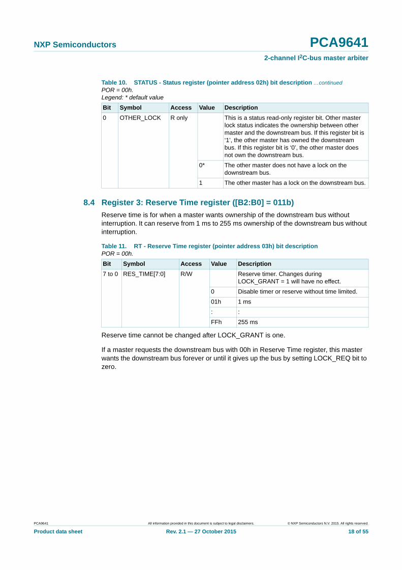
11. Request grant examples
In the waveform shown in Figure 11, Master 0 initiated a START first. Master 1 was at a higher clock speed and wrote the request bit first, so Master 1 won the arbitration.
The effects of the arbitration do not take effect until the winning master issues a STOP condition. If the winning master were to continue to write to the next register using auto-incrementing addresses, it would delay the grant until the STOP. The master has ‘won’ the arbitration, though.
Two masters request the bus at the same time (close enough that the logic cannot tell the difference). See Figure 8 for the waveform. In this case the PRIORITY bits are used to determine the winner. The truth table, Table 9, is for winner selection.
12. Characteristics of the I2C-bus
The information in this section pertains to both M0 and M1 I2C-bus interfaces.
The I2C-bus interface is used to access the device programmable registers. This interface runs as Fast-mode Plus (Fm+) speeds with a general call software reset. The I2C core is composed of the I2C State Machine, shift register, and the start/stop detection logic.
The I2C-bus is for 2-way, 2-line communication between different ICs or modules. The two lines are a serial data line (SDA) and a serial clock line (SCL). Both lines must be connected to a positive supply via a pull-up resistor when connected to the output stages of a device. Data transfer may be initiated only when the bus is not busy.
Fig 11. Request grant example
aaa-008554
ACK
ACKM1 SDA
M1 SCL
M0 SDA
M0 SCL
grant
winner
Master 1
Master 0
none
none
M1
M1
PCA9641 All information provided in this document is subject to legal disclaimers. © NXP Semiconductors N.V. 2015. All rights reserved.
Product data sheet Rev. 2.1 — 27 October 2015 25 of 55

NXP Semiconductors PCA96412-channel I2C-bus master arbiter
12.1 Bit transfer
One data bit is transferred during each clock pulse. The data on the SDA line must remain stable during the HIGH period of the clock pulse as changes in the data line at this time will be interpreted as control signals (see Figure 12).
12.2 START and STOP conditions
Both data and clock lines remain HIGH when the bus is not busy. A HIGH-to-LOW transition of the data line, while the clock is HIGH is defined as the START condition (S). A LOW-to-HIGH transition of the data line while the clock is HIGH is defined as the STOP condition (P) (see Figure 13).
12.3 System configuration
A device generating a message is a ‘transmitter’, a device receiving is the ‘receiver’. The device that controls the message is the ‘master’ and the devices which are controlled by the master are the ‘slaves’ (see Figure 14).
Fig 12. Bit transfer
mba607
data linestable;
data valid
changeof dataallowed
SDA
SCL
Fig 13. Definition of START and STOP conditions
mba608
SDA
SCLP
STOP condition
S
START condition
PCA9641 All information provided in this document is subject to legal disclaimers. © NXP Semiconductors N.V. 2015. All rights reserved.
Product data sheet Rev. 2.1 — 27 October 2015 26 of 55

NXP Semiconductors PCA96412-channel I2C-bus master arbiter
12.4 Acknowledge
The number of data bytes transferred between the START and the STOP conditions from transmitter to receiver is not limited. Each byte of eight bits is followed by one acknowledge bit. The acknowledge bit is a HIGH level put on the bus by the transmitter, whereas the master generates an extra acknowledge related clock pulse.
A slave receiver which is addressed must generate an acknowledge after the reception of each byte. Also a master must generate an acknowledge after the reception of each byte that has been clocked out of the slave transmitter. The device that acknowledges has to pull down the SDA line during the acknowledge clock pulse, so that the SDA line is stable LOW during the HIGH period of the acknowledge related clock pulse; set-up and hold times must be taken into account.
A master receiver must signal an end of data to the transmitter by not generating an acknowledge on the last byte that has been clocked out of the slave. In this event, the transmitter must leave the data line HIGH to enable the master to generate a STOP condition.
Fig 14. System configuration
aaa-012277
MASTERTRANSMITTER/
RECEIVER
SLAVERECEIVER
SLAVETRANSMITTER/
RECEIVER
SDA
SCL
2-CHANNELI2C-BUS
MASTER ARBITERPCA9641
SLAVERECEIVER
SLAVERECEIVER
MASTER 0TRANSMITTER/
RECEIVER
MASTER 1TRANSMITTER/
RECEIVER
SDA 0
SCL 0
SDA 1
SCL 1
Fig 15. Acknowledgement on the I2C-bus
002aaa987
S
STARTcondition
9821
clock pulse foracknowledgement
not acknowledge
acknowledge
data outputby transmitter
data outputby receiver
SCL from master
PCA9641 All information provided in this document is subject to legal disclaimers. © NXP Semiconductors N.V. 2015. All rights reserved.
Product data sheet Rev. 2.1 — 27 October 2015 27 of 55

NXP Semiconductors PCA96412-channel I2C-bus master arbiter
12.5 Bus transactions
Fig 16. Write to the Interrupt Enable and Control registers using the Auto-Increment (AI) bit
aaa-008571
A6 A5 A4 A3 A2 A1 A0 0
slave address
R/W
S
START condition
A
acknowledgefrom slave
1 0 0 0 0 0 0 1
command code register
auto increment
A
acknowledgefrom slave
A P
STOPcondition
A
acknowledgefrom slave
acknowledgefrom slave
dataControl register
(CONTR)
dataReserve Time register
(RT)
A
acknowledgefrom slave
dataStatus register
(STATUS)
PCA9641 All information provided in this document is subject to legal disclaimers. © NXP Semiconductors N.V. 2015. All rights reserved.
Product data sheet Rev. 2.1 — 27 October 2015 28 of 55

NXP Semiconductors PCA96412-channel I2C-bus master arbiter
12.6 Auto-increment
Writing to each register carries an overhead of a total of 3 bytes: slave address, command, and data. Auto-increment allows the user to send or receive data continuously where the slave will auto-increment and wrap around on the registers.
The auto-increment is bit 8 of the command byte (see Figure 5).
By setting the AI bit to 1, the master can send or read N data bytes to or from incrementing addresses that wrap around to 0x0. For example, a write to register address 0x4 will write data byte 1 to address 0x4, data byte 2 to address 0x5 data byte 3 to address 0x6, data byte 4 to address 0x7, data byte 5 to address 0x0, data byte 6 to address 0x1, data byte 7 to address 0x2 and data byte 8 to address 0x3. The read occurs in much the same way. When write to read register only, the write will not affect the value.
The master stops an auto-increment write by sending a STOP bit after the final slave ACK. The master stops a read by NACKing the final byte and sending a STOP bit.
Remark: If an eighth data byte is read, the first register will be accessed.
Refer to Table 15.
Fig 17. Read the five registers using the Auto-Increment (AI) bit
aaa-008572
A6 A5 A4 A3 A2 A1 A0 0
slave address
R/W
S
START condition
A
acknowledgefrom slave
1 0 0 0 0 x x x
command code registeraccess to register
xxx = 000, 001, 010, 011, 100, 101, 110 or 111
autoincrement
A
acknowledgefrom slave
A P
STOPcondition
A
no acknowledgefrom master
acknowledgefrom master
Sr
re-STARTcondition
A6 A5 A4 A3 A2 A1 A0 1
slave address
R/W
A
acknowledgefrom slave
eighth data bytesecond data byte
A
acknowledgefrom master
first data byte
A
acknowledgefrom master
third data byte
Table 15. Read/write the registers using Auto-Increment
Command code
First data byte
Second data byte
Third data byte
Fourth data byte
Fifth data byte
Sixth data byte
Seventh data byte
Eighth data byte
1000 0000 ID CONTR STATUS RT INT_STATUS
INT_MASK MB_LO MB_HI
1000 0001 CONTR STATUS RT INT_STATUS
INT_MASK MB_LO MB_HI ID
1000 0010 STATUS RT INT_STATUS
INT_MASK MB_LO MB_HI ID CONTR
1000 0011 RT INT_STATUS
INT_MASK MB_LO MB_HI ID CONTR STATUS
1000 0100 INT_STATUS
INT_MASK MB_LO MB_HI ID CONTR STATUS RT
PCA9641 All information provided in this document is subject to legal disclaimers. © NXP Semiconductors N.V. 2015. All rights reserved.
Product data sheet Rev. 2.1 — 27 October 2015 29 of 55

NXP Semiconductors PCA96412-channel I2C-bus master arbiter
13. General call software reset
The Software Reset Call allows all the devices in the I2C-bus to be reset to the power-up state value through a specific formatted I2C-bus command. To be performed correctly, it implies that the I2C-bus is functional and that there is no device hanging the bus.
The Software Reset sequence is defined as following:
1. A START command is sent by the I2C-bus master.
2. The reserved General Call I2C-bus address ‘0000 000’ with the R/W bit set to 0 (write) is sent by the I2C-bus master.
3. The device(s) acknowledge(s) after seeing the General Call address ‘0000 0000’ (00h) only. If the R/W bit is set to 1 (read), no acknowledge is returned to the I2C-bus master.
4. Once the General Call address has been sent and acknowledged, the master sends 1 byte. The value of the byte must be equal to 06h. The device acknowledges this value only. If the byte is not equal to 06h, the device does not acknowledge it. If more than 1 byte of data is sent, the device does not acknowledge any more.
5. Once the right byte has been sent and correctly acknowledged, the master sends a STOP command to end the Software Reset sequence: the slave device then resets to the default value (power-up value) and is ready to be addressed again within the specified bus free time. If the master sends a Repeated START instead, no reset is performed.
6. PCA9641 will issue the bus recovery procedure.
The I2C-bus master must interpret a non-acknowledge from the slave device (at any time) as a ‘Software Reset Abort’. Slave device does not initiate a reset of its registers.
1000 0101 INT_MASK MB_LO MB_HI ID CONTR STATUS RT INT_STATUS
1000 0110 MB_LO MB_HI ID CONTR STATUS RT INT_STATUS
INT_MASK
1000 0111 MB_HI ID CONTR STATUS RT INT_STATUS
INT_MASK MB_LO
Table 15. Read/write the registers using Auto-Increment …continued
Command code
First data byte
Second data byte
Third data byte
Fourth data byte
Fifth data byte
Sixth data byte
Seventh data byte
Eighth data byte
Fig 18. Software Reset sequence
aaa-008555
0 0 0 0 0 0 0 AS 0
SWRST Call I2C-bus address
START condition R/W
acknowledgefrom slave(s)
0 0 0 0 1 1 00
SWRST data = 06h
A
acknowledgefrom slave(s)
P
PCA9641 is reset.Registers are set to default power-up values.
PCA9641 All information provided in this document is subject to legal disclaimers. © NXP Semiconductors N.V. 2015. All rights reserved.
Product data sheet Rev. 2.1 — 27 October 2015 30 of 55
NXP Semiconductors PCA96412-channel I2C-bus master arbiter
14. Device ID (PCA9641 ID field)
The Device ID field is a 3-byte read-only (24 bits) word giving the following information:
• The first 12 bits are for the manufacturer name, unique per manufacturer (for example, NXP).
• The next 9 bits are for the part identification, assigned by manufacturer.
• The last 3 bits are for the die revision, assigned by manufacturer (for example, Rev X).
The Device ID is read-only, hardwired in the device and can be accessed as follows:
1. START command.
2. The master sends the Reserved Device ID I2C-bus address ‘1111 100’ with the R/W bit set to 0 (write).
3. The master sends the I2C-bus slave address of the slave device it needs to identify. The LSB is a ‘Don’t care’ value. Only one device must acknowledge this byte (the one that has the I2C-bus slave address).
4. The master sends a Re-START command.
Remark: A STOP command followed by a START command will reset the slave state machine and the Device ID read cannot be performed.
Remark: A STOP command or a Re-START command followed by an access to another slave device will reset the slave state machine and the Device ID read cannot be performed.
5. The master sends the Reserved Device ID I2C-bus address ‘1111 100’ with the R/W bit set to 1 (read).
6. The device ID read can be done, starting with the 12 manufacturer bits (first byte + 4 MSB of the second byte), followed by the 9 part identification bits and then the 3 die revision bits (3 LSB of the third byte).
7. The master ends the reading sequence by NACKing the last byte, thus resetting the slave device state machine and allowing the master to send the STOP command.
Remark: The reading of the Device ID can be stopped anytime by sending a NACK command.
Remark: If the master continues to ACK the bytes after the third byte, the PCA9641 rolls back to the first byte and keeps sending the Device ID sequence until a NACK has been detected.
Table 16. PCA9641 ID field
Byte 3 Byte 2 Byte 1
0 0 0 0 0 0 0 0 0 0 0 0 1 0 0 0 0 0 1 1 1 0 0 0
Bits [23:11] Bits [10:3] Bits [2:0]
Manufacturer ID Part ID Revision
PCA9641 All information provided in this document is subject to legal disclaimers. © NXP Semiconductors N.V. 2015. All rights reserved.
Product data sheet Rev. 2.1 — 27 October 2015 31 of 55

NXP Semiconductors PCA96412-channel I2C-bus master arbiter
15. Shared mailbox
Shared mailbox contains two 8-bit bidirectional mailboxes used for communication between the two masters. Each master has MB_HI and MB_LO registers on their address map. The mailbox uses a MBOX_FULL and MBOX_EMPTY status to assist in the flow of data and prevent data loss or corruption.
When a master is sending data via the mailbox, it must check the MBOX_EMPTY status bit. If the MBOX_EMPTY status bit is zero (not EMPTY), then it contains data for the other master that has not been read, and writing at this time would result in data loss/corruption. When the MBOX_EMPTY status bit is one (EMPTY), the master may write to the mailbox. In order to send data through the mailbox, the master must write the entire 16 bits, starting with MB_LO and finishing with MB_HI. If the mailbox is written in reverse order, it will not activate the FULL flag on the receiving master. Once the mailbox has been written, the transmitting master’s MBOX_EMPTY status bit is cleared (0), and the receiving master’s MBOX_FULL status bit is set (1).
When a master’s MBOX_FULL status bit is set, it means that there is data in the mailbox from the other master that has not been read. The master may read the mailbox in any order, but the FULL flag will not be cleared until both MB_LO and MB_HI have been read. When they have been read, the sending master’s MBOX_EMPTY status bit is set, indicating the data has been read and the mailbox is ready for more data. When they have been read, the receiving master’s MBOX_FULL status bit is cleared, indicating there is no new data in the mailbox to be read.
When a master writes the mailbox registers, it is sending data to the other master’s mailbox. When a master reads the mailbox, it is reading from its own mailbox. It is not possible to write data into the mailbox and read it back.
Fig 19. Shared mailbox byte arrangement
A
aaa-008573
D6 D5 D4 D3 D2 D1 D0
MB_LOW
D7 AD14 D13 D12 D11 D10 D9 D8
MB_HI
D15
PCA9641 All information provided in this document is subject to legal disclaimers. © NXP Semiconductors N.V. 2015. All rights reserved.
Product data sheet Rev. 2.1 — 27 October 2015 32 of 55

NXP Semiconductors PCA96412-channel I2C-bus master arbiter
16. Application design-in information
Fig 20. Typical application
PCA9641
SCL_MST0
SDA_MST0
INT0
2.5 V
MASTER 0
002aag819
SCL0
SDA0
INT0 INT_IN
A3
A2
A1
VDD
A0VSS
VDD
RESET0
VSS
SLAVE 1SDA SCL
SLAVE 2
SDA SCLINT
SLAVE 3SDA SCL
SDA_SLAVE
SCL_SLAVE
SCL_MST1
SDA_MST1
INT1
1.8 V
MASTER 1SCL1
SDA1
INT1
VDD
RESET1
VSS
RESET
SLAVE CARD3.3 V
3.3 V
PCA9641 All information provided in this document is subject to legal disclaimers. © NXP Semiconductors N.V. 2015. All rights reserved.
Product data sheet Rev. 2.1 — 27 October 2015 33 of 55

NXP Semiconductors PCA96412-channel I2C-bus master arbiter
16.1 Specific applications
The PCA9641 is a 2-to-1 I2C-bus master arbiter designed for dual masters sharing the same downstream slave devices. Any master can request the downstream bus at any time and PCA9641 will let the master know when it is its turn to control the downstream bus. The master will not overwrite the other master’s transactions, and no advance software is needed. In high reliability I2C-bus applications, the PCA9641 will switch between masters when the downstream bus is free and clear. If the downstream bus hangs, PCA9641 will remotely recover the bus by multiple ways, such as smart initialization, SMBus time-out, remote toggling of SCL and SDA.
16.2 High reliability systems
In a typical multipoint application, shown in Figure 22, the two masters (for example, primary and back-up) are located on separate I2C-buses that connect to multiple downstream I2C-bus slave cards/devices via a PCA9641 for non-hot swap applications to provide high reliability of the I2C-bus.
I2C-bus commands are sent via the primary or back-up master and either master can take command of the I2C-bus. Either master at any time can gain control of the slave devices if the other master is disabled or removed from the system. The failed master is isolated from the system and will not affect communication between the on-line master and the slave devices located on the cards.
For even higher reliability in multipoint backplane applications, two dedicated masters can be used for every card as shown in Figure 23.
Fig 21. Arbitration application
aaa-009751
Master 0 M0-Trans3 M0-Trans2 M0-Trans1 I2C M0
PCA9641ARBITER
I2C M1M0-Trans1M1-Trans2Master 1
t1 M0-Trans3 M1-Trans2
Slave 1
Slave 0
t1M0-Trans2 M0-Trans1
Slave 2
Slave 3 Slave 4
M0-Trans1
Fig 22. High reliability backplane application
002aag820
MA
STE
R 1
SCL1SDA1M
AS
TER
0
PCA
9641
PCA
9641
PCA
9641
PCA
9641
PCA
9641
PCA
9641
PCA
9641
PCA
9641
SCL0SDA0
PCA9641 All information provided in this document is subject to legal disclaimers. © NXP Semiconductors N.V. 2015. All rights reserved.
Product data sheet Rev. 2.1 — 27 October 2015 34 of 55

NXP Semiconductors PCA96412-channel I2C-bus master arbiter
16.3 Masters with shared resources
Some masters may not be multi-master capable or some masters may not work well together and continually lock up the bus. The PCA9641 can be used to separate the masters, as shown in Figure 24, but still allow shared access to slave devices, such as Field Replaceable Unit (FRU) EEPROMs or temperature sensors.
Fig 23. Very high reliability backplane application
002aag821
SCL1SDA1
MA
STE
R 0
PCA
9641
SCL0SDA0
MA
STE
R 0
MA
STE
R 0
MA
STE
R 0
SCL0SDA0
SCL0SDA0
SCL0SDA0
MA
STE
R 1
MA
STE
R 1
MA
STE
R 1
MA
STE
R 1
SCL1SDA1
SCL1SDA1
SCL1SDA1
PCA
9641
PCA
9641
PCA
9641
Fig 24. Masters with shared resources application
002aag822
PCA9641
SLAVE A0
SLAVE A1 SLAVE A2
MASTER A
PCA9641
SLAVE B0
SLAVE B1 SLAVE B2
MASTER B
ASSEMBLY A
ASSEMBLY B
SDA/SCL
SDA/SCL
MAINMASTER
PCA9641 All information provided in this document is subject to legal disclaimers. © NXP Semiconductors N.V. 2015. All rights reserved.
Product data sheet Rev. 2.1 — 27 October 2015 35 of 55

NXP Semiconductors PCA96412-channel I2C-bus master arbiter
16.4 Gatekeeper multiplexer
The PCA9641 can act as a gatekeeper multiplexer in applications where there are multiple I2C-bus devices with the same fixed address (for example, EEPROMs with address of ‘Z’ as shown in Figure 25) connected in a multipoint arrangement to the same I2C-bus. Up to 112 hot-swappable cards/devices can be multiplexed to the same bus master by using one PCA9641 per card/device. Since each PCA9641 has its own unique address (for example, ‘A’, ‘B’, ‘C’, and so on), the EEPROMs can be connected to the master, one at a time, by connecting one PCA9641 (Master 0 position) while keeping the rest of the cards/devices isolated (off position).
The alternative, shown with dashed lines, is to use a PCA9548A 1-to-8 channel switch on the master card and run eight I2C-bus devices, one to each EEPROM card, to multiplex the master to each card. The number of card pins used is the same in either case, but there are seven fewer pairs of SDA/SCL traces on the printed-circuit board if the PCA9641 is used.
Fig 25. Gatekeeper multiplexer application
002aag823
MA
STE
R 0
PCA
9641
PC
A95
48A
EE
PR
OM
Z
A
PCA
9641
EE
PR
OM
Z
B
PCA
9641
EE
PR
OM
Z
C
PCA
9641
EE
PR
OM
Z
D
PCA
9641
EE
PR
OM
Z
E
PCA
9641
EE
PR
OM
Z
F
PCA
9641
EE
PR
OM
Z
G
PCA
9641
EE
PR
OM
Z
H
PCA9641 All information provided in this document is subject to legal disclaimers. © NXP Semiconductors N.V. 2015. All rights reserved.
Product data sheet Rev. 2.1 — 27 October 2015 36 of 55

NXP Semiconductors PCA96412-channel I2C-bus master arbiter
16.5 Bus initialization/recovery to initialize slaves without hardware reset
If the I2C-bus is hung, I2C-bus devices without a hardware reset pin (for example, Slave 1 and Slave 2 in Figure 26) can be isolated from the master by the PCA9641. The PCA9641 disconnects the hung bus if IDLE_TIMER_DIS was set or over 500 ms, restoring the master's control of the rest of the bus (for example, Slave 0). The bus master can then command the PCA9641 to send nine clock pulses/STOP condition to reset the downstream I2C-bus devices before they are reconnected to the master or leave the downstream devices isolated.
16.6 Power-on reset requirements
In the event of a glitch or data corruption, PCA9641 can be reset to its default conditions by using the power-on reset feature. Power-on reset requires that the device go through a power cycle to be completely reset. This reset also happens when the device is powered on for the first time in an application.
The two types of power-on reset are shown in Figure 27 and Figure 28.
Fig 26. Bus initialization/recovery application
002aag824
PCA9641
SLAVE 1
SDASCL
SLAVE 2
slave I2C-bus
MASTER
SLAVE 0
RESET
SDA/SCL
Fig 27. VDD is lowered below 0.7 V or 0 V and then ramped up to VDD
Fig 28. VDD is lowered below the POR threshold, then ramped back up to VDD
aaa-013905
VDD
time
ramp-up ramp-down
(dV/dt)r (dV/dt)f
re-ramp-up
(dV/dt)rtime to re-rampwhen VDD drops
below 0.7 V or to VSS
td(rst)
002aah330
VDD
time
ramp-down
(dV/dt)f
ramp-up
(dV/dt)rtime to re-ramp
when VDD dropsto VPOR(min) − 50 mV
td(rst)VI drops below POR levels
PCA9641 All information provided in this document is subject to legal disclaimers. © NXP Semiconductors N.V. 2015. All rights reserved.
Product data sheet Rev. 2.1 — 27 October 2015 37 of 55

NXP Semiconductors PCA96412-channel I2C-bus master arbiter
Table 17 specifies the performance of the power-on reset feature for PCA9641 for both types of power-on reset.
[1] Glitch width and VDD voltage that will not cause a functional disruption.
Glitches in the power supply can also affect the power-on reset performance of this device. The glitch width (tw(gl)VDD) and glitch height (VDD(gl)) are dependent on each other. The bypass capacitance, source impedance, and device impedance are factors that affect power-on reset performance. Figure 29 and Table 17 provide more information on how to measure these specifications.
VPOR is critical to the power-on reset. VPOR is the voltage level at which the reset condition is released and all the registers and the I2C-bus/SMBus state machine are initialized to their default states. The value of VPOR differs based on the VDD being lowered to or from 0 V. Figure 30 and Table 17 provide more details on this specification.
Table 17. Recommended supply sequencing and ramp ratesTamb = 25 C (unless otherwise noted). Not tested; specified by design.
Symbol Parameter Condition Min Typ Max Unit
(dV/dt)f fall rate of change of voltage Figure 27 0.1 - 2000 ms
(dV/dt)r rise rate of change of voltage Figure 27 0.1 - 2000 ms
td(rst) reset delay time Figure 27; re-ramp time when VDD drops to VSS
1 - - s
Figure 28; re-ramp time when VDD drops to VPOR(min) 50 mV
1 - - s
VDD(gl) glitch supply voltage difference Figure 29 [1] - - 1 V
tw(gl)VDD supply voltage glitch pulse width Figure 29 [1] - - 10 s
VPOR(trip) power-on reset trip voltage falling VDD 0.7 - - V
rising VDD - - 1.8 V
tREC;STA recovery time to START condition refer to Figure 33 155 - - s
Fig 29. Glitch width and glitch height
002aah331
VDD
timetw(gl)VDD
∆VDD(gl)
PCA9641 All information provided in this document is subject to legal disclaimers. © NXP Semiconductors N.V. 2015. All rights reserved.
Product data sheet Rev. 2.1 — 27 October 2015 38 of 55

NXP Semiconductors PCA96412-channel I2C-bus master arbiter
17. Limiting values
[1] The performance capability of a high-performance integrated circuit in conjunction with its thermal environment can create junction temperatures which are detrimental to reliability. The maximum junction temperature of this integrated circuit should not exceed 125 C.
Fig 30. Power-on reset voltage (VPOR)
002aah332
POR
time
VDD
time
VPOR (rising VDD)
VPOR (falling VDD)
Table 18. Limiting valuesIn accordance with the Absolute Maximum Rating System (IEC 60134).Voltages are referenced to VSS (ground = 0 V).[1]
Symbol Parameter Conditions Min Max Unit
VDD supply voltage 0.5 +4.0 V
VI input voltage 0.5 +4.0 V
II input current 20 +20 mA
IO output current 25 +25 mA
IDD supply current 100 +100 mA
ISS ground supply current 100 +100 mA
Ptot total power dissipation - 400 mW
Tstg storage temperature 60 +150 C
Tamb ambient temperature operating in free air 40 +85 C
PCA9641 All information provided in this document is subject to legal disclaimers. © NXP Semiconductors N.V. 2015. All rights reserved.
Product data sheet Rev. 2.1 — 27 October 2015 39 of 55

NXP Semiconductors PCA96412-channel I2C-bus master arbiter
18. Static characteristics
Table 19. Static characteristicsVDD = 2.3 V to 3.6 V; VSS = 0 V; Tamb = 40 C to +85 C; unless otherwise specified.
Symbol Parameter Conditions Min Typ Max Unit
Supply
VDD supply voltage 2.3 - 3.6 V
IDD supply current Operating mode; no load; VI = VDD or VSS; fSCL = 1 MHz; RESET VDD
[6]
VDD = 2.3 V - 127[4] 210[5] A
VDD = 3.6 V - 184[2] 325 A
Istb standby current Standby mode; no load; VI = VDD or VSS; fSCL = 0 kHz; RESET VDD
[6]
VDD = 2.3 V - 110[4] 160[5] A
VDD = 3.6 V - 148[2] 275 A
VPOR power-on reset voltage no load; VI = VDD or VSS[1] - 1.5 2.1 V
Input SCL_MSTn; input/output SDA_MSTn (upstream and downstream channels)
VIL LOW-level input voltage 0.5 - +0.3VDD V
VIH HIGH-level input voltage 0.7VDD - 3.6 V
IOL LOW-level output current VOL = 0.4 V 20 38[2] - mA
IL leakage current VI = VDD or VSS 1 - +1 A
Ci input capacitance VI = VSS
VDD = 2.3 V to 3.6 V[5] - 6 10 pF
Select inputs A0 to A3[3]
ILI input leakage current VI = VDD or VSS 1 - +1 A
Ci input capacitance VI = VSS
VDD = 2.3 V to 3.6 V[5] - 4 10 pF
Select inputs INT_IN, RESET
VIL LOW-level input voltage 0.5 - +0.3VDD V
VIH HIGH-level input voltage 0.7VDD - 3.6 V
ILI input leakage current VI = VDD or VSS 1 - +1 A
Ci input capacitance VI = VSS
VDD = 2.3 V to 3.6 V[5] - 4 10 pF
PCA9641 All information provided in this document is subject to legal disclaimers. © NXP Semiconductors N.V. 2015. All rights reserved.
Product data sheet Rev. 2.1 — 27 October 2015 40 of 55

NXP Semiconductors PCA96412-channel I2C-bus master arbiter
[1] VDD must be lowered to 0.7 V in order to reset part
[2] Typical VDD = 3.0 V at room temperature
[3] See Table 4
[4] Typical VDD = 2.3 V at room temperature, nominal device
[5] Guaranteed by characterization
[6] When RESET = VSS, IDD and Istb increase approximately 4.5 mA
19. Dynamic characteristics
Pass gate
Ron ON-state resistance VO = 0.4 V; IO = 20 mA
VDD = 3.0 V to 3.6 V - 7.9[2] 11.5
VDD = 2.3 V to 2.7 V - 9.9[4] 14.5
Vo(sw) switch output voltage Io(sw) = 100 A
Vi(sw) = VDD = 3.6 V 1.6 2.0[2] 2.8 V
Vi(sw) = VDD = 2.3 V 1.1 1.4[4] 2.2 V
IL leakage current VI = VDD or VSS 1 - +1 A
INT0 and INT1 outputs
IOL LOW-level output current VOL = 0.4 V 3 - - mA
Table 19. Static characteristics …continuedVDD = 2.3 V to 3.6 V; VSS = 0 V; Tamb = 40 C to +85 C; unless otherwise specified.
Symbol Parameter Conditions Min Typ Max Unit
Table 20. Dynamic characteristics
Symbol Parameter Conditions Standard-modeI2C-bus
Fast-modeI2C-bus
Fast-mode PlusI2C-bus
Unit
Min Max Min Max Min Max
tPD propagation delay (SDA_MSTn to SDA_SLAVE) or (SCL_MSTn to SCL_SLAVE)
[1] - 0.3 - 0.3 - 0.3 ns
fSCL SCL clock frequency
20 100 20 400 20 1000 kHz
fSCL(init/rec) SCL clock frequency (bus initialization/bus recovery)
[8] 18 50 18 50 18 50 kHz
tBUF bus free time between a STOP and START condition
4.7 - 1.3 - 0.5 - s
tHD;STA hold time (repeated) START condition
[2] 4.0 - 0.6 - 0.26 - s
tLOW LOW period of the SCL clock
4.7 - 1.3 - 0.5 - s
tHIGH HIGH period of the SCL clock
4.0 - 0.6 - 0.26 - s
PCA9641 All information provided in this document is subject to legal disclaimers. © NXP Semiconductors N.V. 2015. All rights reserved.
Product data sheet Rev. 2.1 — 27 October 2015 41 of 55

NXP Semiconductors PCA96412-channel I2C-bus master arbiter
[1] Pass gate propagation delay is calculated from the 20 typical Ron and the 15 pF load capacitance.
[2] After this period, the first clock pulse is generated.
[3] A device must internally provide a hold time of at least 300 ns for the SDA signal (referred to the VIH(min) of the SCL signal) in order to bridge the undefined region of the falling edge of SCL.
[4] Cb = total capacitance of one bus line in pF.
[5] Measurements taken with 1 k pull-up resistor and 50 pF load.
[6] Resetting the device while actively communicating on the bus may cause glitches or errant STOP conditions.
[7] Upon reset, the full delay will be the sum of trst and the RC time constant of the SDA bus.
[8] Guaranteed by characterization.
tSU;STA set-up time for a repeated START condition
4.7 - 0.6 - 0.26 - s
tSU;STO set-up time for STOP condition
4.0 - 0.6 - 0.26 - s
tHD;DAT data hold time 0[3] 3.45 0[3] 0.9 0[3] - s
tSU;DAT data set-up time 250 - 100 - 50 - ns
tr rise time of both SDA and SCL signals
- 1000 20 300 - 120 ns
tf fall time of both SDA and SCL signals
- 300 20 (VDD / 3.3 V)
300 20 (VDD / 3.3 V)
120 ns
Cb capacitive load for each bus line
[4] - 400 - 400 - 500 pF
tSP pulse width of spikes that must be suppressed by the input filter
- 50 - 50 - 50 ns
tVD;DAT data valid time [5] - 1 - 1 0.05 0.45 s
tVD;ACK data valid acknowledge time
- 1 - 1 0.05 0.45 s
INT
tv(INT_IN-INTn) valid time from pin INT_IN to pin INTn signal
- 4 - 4 - 4 s
tw(rej)L LOW-level rejection time
INT_IN input 0.05 - 0.05 - 0.05 - s
RESET
tw(rst)L LOW-level reset time
10 - 10 - 10 - ns
trst reset time SDA clear 500 - 500 - 500 - ns
tREC;STA recovery time to START condition
[6][7] 90 - 90 - 90 - s
Table 20. Dynamic characteristics …continued
Symbol Parameter Conditions Standard-modeI2C-bus
Fast-modeI2C-bus
Fast-mode PlusI2C-bus
Unit
Min Max Min Max Min Max
PCA9641 All information provided in this document is subject to legal disclaimers. © NXP Semiconductors N.V. 2015. All rights reserved.
Product data sheet Rev. 2.1 — 27 October 2015 42 of 55

NXP Semiconductors PCA96412-channel I2C-bus master arbiter
Fig 31. Definition of timing on the I2C-bus
tSPtBUF
tHD;STAPP S
tLOW
tr
tHD;DAT
tf
tHIGH tSU;DATtSU;STA
Sr
tHD;STA
tSU;STO
SDA
SCL
002aaa986
0.7 × VDD
0.3 × VDD
0.7 × VDD
0.3 × VDD
Rise and fall times, refer to VIL and VIH.
Fig 32. I2C-bus timing diagram
002aab175
protocolSTART
condition(S)
bit 7MSB(A7)
bit 6(A6)
bit 0(R/W)
acknowledge(A)
STOPcondition
(P)
SCL
SDA
tHD;STA tSU;DAT tHD;DAT
tftBUF
tSU;STA tLOW tHIGH
tVD;ACK tSU;STO
1 / fSCL
tr
tVD;DAT
0.3 × VDD
0.7 × VDD
0.3 × VDD
0.7 × VDD
Fig 33. Definition of RESET timing
SDA
SCL
002aae735
trst
50 %
30 %
50 % 50 %
50 %
tREC;STA tw(rst)L
RESET
INTn
START
trst
ACK or read cycle
PCA9641 All information provided in this document is subject to legal disclaimers. © NXP Semiconductors N.V. 2015. All rights reserved.
Product data sheet Rev. 2.1 — 27 October 2015 43 of 55

NXP Semiconductors PCA96412-channel I2C-bus master arbiter
20. Test information
Definitions test circuit:
RL = Load resistance.
CL = Load capacitance including jig and probe capacitance.
RT = Termination resistance should be equal to the output impedance Zo of the pulse generator.
Fig 34. Test circuitry for switching times
PULSEGENERATOR
VO
CL50 pF
RL500 Ω
002aab393
RT
VI
VDD
DUT
6.0 VopenVSS
PCA9641 All information provided in this document is subject to legal disclaimers. © NXP Semiconductors N.V. 2015. All rights reserved.
Product data sheet Rev. 2.1 — 27 October 2015 44 of 55

NXP Semiconductors PCA96412-channel I2C-bus master arbiter
21. Package outline
Fig 35. Package outline SOT403-1 (TSSOP16)
PCA9641 All information provided in this document is subject to legal disclaimers. © NXP Semiconductors N.V. 2015. All rights reserved.
Product data sheet Rev. 2.1 — 27 October 2015 45 of 55

NXP Semiconductors PCA96412-channel I2C-bus master arbiter
Fig 36. Package outline SOT758-1 (HVQFN16)
PCA9641 All information provided in this document is subject to legal disclaimers. © NXP Semiconductors N.V. 2015. All rights reserved.
Product data sheet Rev. 2.1 — 27 October 2015 46 of 55

NXP Semiconductors PCA96412-channel I2C-bus master arbiter
22. Soldering of SMD packages
This text provides a very brief insight into a complex technology. A more in-depth account of soldering ICs can be found in Application Note AN10365 “Surface mount reflow soldering description”.
22.1 Introduction to soldering
Soldering is one of the most common methods through which packages are attached to Printed Circuit Boards (PCBs), to form electrical circuits. The soldered joint provides both the mechanical and the electrical connection. There is no single soldering method that is ideal for all IC packages. Wave soldering is often preferred when through-hole and Surface Mount Devices (SMDs) are mixed on one printed wiring board; however, it is not suitable for fine pitch SMDs. Reflow soldering is ideal for the small pitches and high densities that come with increased miniaturization.
22.2 Wave and reflow soldering
Wave soldering is a joining technology in which the joints are made by solder coming from a standing wave of liquid solder. The wave soldering process is suitable for the following:
• Through-hole components
• Leaded or leadless SMDs, which are glued to the surface of the printed circuit board
Not all SMDs can be wave soldered. Packages with solder balls, and some leadless packages which have solder lands underneath the body, cannot be wave soldered. Also, leaded SMDs with leads having a pitch smaller than ~0.6 mm cannot be wave soldered, due to an increased probability of bridging.
The reflow soldering process involves applying solder paste to a board, followed by component placement and exposure to a temperature profile. Leaded packages, packages with solder balls, and leadless packages are all reflow solderable.
Key characteristics in both wave and reflow soldering are:
• Board specifications, including the board finish, solder masks and vias
• Package footprints, including solder thieves and orientation
• The moisture sensitivity level of the packages
• Package placement
• Inspection and repair
• Lead-free soldering versus SnPb soldering
22.3 Wave soldering
Key characteristics in wave soldering are:
• Process issues, such as application of adhesive and flux, clinching of leads, board transport, the solder wave parameters, and the time during which components are exposed to the wave
• Solder bath specifications, including temperature and impurities
PCA9641 All information provided in this document is subject to legal disclaimers. © NXP Semiconductors N.V. 2015. All rights reserved.
Product data sheet Rev. 2.1 — 27 October 2015 47 of 55

NXP Semiconductors PCA96412-channel I2C-bus master arbiter
22.4 Reflow soldering
Key characteristics in reflow soldering are:
• Lead-free versus SnPb soldering; note that a lead-free reflow process usually leads to higher minimum peak temperatures (see Figure 37) than a SnPb process, thus reducing the process window
• Solder paste printing issues including smearing, release, and adjusting the process window for a mix of large and small components on one board
• Reflow temperature profile; this profile includes preheat, reflow (in which the board is heated to the peak temperature) and cooling down. It is imperative that the peak temperature is high enough for the solder to make reliable solder joints (a solder paste characteristic). In addition, the peak temperature must be low enough that the packages and/or boards are not damaged. The peak temperature of the package depends on package thickness and volume and is classified in accordance with Table 21 and 22
Moisture sensitivity precautions, as indicated on the packing, must be respected at all times.
Studies have shown that small packages reach higher temperatures during reflow soldering, see Figure 37.
Table 21. SnPb eutectic process (from J-STD-020D)
Package thickness (mm) Package reflow temperature (C)
Volume (mm3)
< 350 350
< 2.5 235 220
2.5 220 220
Table 22. Lead-free process (from J-STD-020D)
Package thickness (mm) Package reflow temperature (C)
Volume (mm3)
< 350 350 to 2000 > 2000
< 1.6 260 260 260
1.6 to 2.5 260 250 245
> 2.5 250 245 245
PCA9641 All information provided in this document is subject to legal disclaimers. © NXP Semiconductors N.V. 2015. All rights reserved.
Product data sheet Rev. 2.1 — 27 October 2015 48 of 55

NXP Semiconductors PCA96412-channel I2C-bus master arbiter
For further information on temperature profiles, refer to Application Note AN10365 “Surface mount reflow soldering description”.
MSL: Moisture Sensitivity Level
Fig 37. Temperature profiles for large and small components
001aac844
temperature
time
minimum peak temperature= minimum soldering temperature
maximum peak temperature= MSL limit, damage level
peak temperature
PCA9641 All information provided in this document is subject to legal disclaimers. © NXP Semiconductors N.V. 2015. All rights reserved.
Product data sheet Rev. 2.1 — 27 October 2015 49 of 55

NXP Semiconductors PCA96412-channel I2C-bus master arbiter
23. Soldering: PCB footprints
Fig 38. PCB footprint for SOT403-1 (TSSOP16); reflow soldering
PCA9641 All information provided in this document is subject to legal disclaimers. © NXP Semiconductors N.V. 2015. All rights reserved.
Product data sheet Rev. 2.1 — 27 October 2015 50 of 55

NXP Semiconductors PCA96412-channel I2C-bus master arbiter
Fig 39. PCB footprint for SOT758-1 (HVQFN16); reflow soldering
PCA9641 All information provided in this document is subject to legal disclaimers. © NXP Semiconductors N.V. 2015. All rights reserved.
Product data sheet Rev. 2.1 — 27 October 2015 51 of 55
NXP Semiconductors PCA96412-channel I2C-bus master arbiter
24. Abbreviations
25. Revision history
Table 23. Abbreviations
Acronym Description
AI Auto Increment
CDM Charged Device Model
DUT Device Under Test
EEPROM Electrically Erasable Programmable Read-Only Memory
ESD ElectroStatic Discharge
FRU Field Replaceable Unit
HBM Human Body Model
I2C-bus Inter Integrated Circuit bus
IC Integrated Circuit
POR Power-On Reset
RC Resistor-Capacitor network
SMBus System Management Bus
Table 24. Revision history
Document ID Release date Data sheet status Change notice Supersedes
PCA9641 v.2.1 20151027 Product data sheet - PCA90641 v.2
Modifications: • Table 20: Corrected tREC;STA from 155 ms to 90 us
PCA9641 v.2 20141010 Product data sheet - PCA90641 v.1
• Modifications: • Corrected Figure 1, Figure 2, Figure 3, Figure 21 and Figure 26
PCA9641 v.1 20141008 Product data sheet - -
PCA9641 All information provided in this document is subject to legal disclaimers. © NXP Semiconductors N.V. 2015. All rights reserved.
Product data sheet Rev. 2.1 — 27 October 2015 52 of 55

NXP Semiconductors PCA96412-channel I2C-bus master arbiter
26. Legal information
26.1 Data sheet status
[1] Please consult the most recently issued document before initiating or completing a design.
[2] The term ‘short data sheet’ is explained in section “Definitions”.
[3] The product status of device(s) described in this document may have changed since this document was published and may differ in case of multiple devices. The latest product status information is available on the Internet at URL http://www.nxp.com.
26.2 Definitions
Draft — The document is a draft version only. The content is still under internal review and subject to formal approval, which may result in modifications or additions. NXP Semiconductors does not give any representations or warranties as to the accuracy or completeness of information included herein and shall have no liability for the consequences of use of such information.
Short data sheet — A short data sheet is an extract from a full data sheet with the same product type number(s) and title. A short data sheet is intended for quick reference only and should not be relied upon to contain detailed and full information. For detailed and full information see the relevant full data sheet, which is available on request via the local NXP Semiconductors sales office. In case of any inconsistency or conflict with the short data sheet, the full data sheet shall prevail.
Product specification — The information and data provided in a Product data sheet shall define the specification of the product as agreed between NXP Semiconductors and its customer, unless NXP Semiconductors and customer have explicitly agreed otherwise in writing. In no event however, shall an agreement be valid in which the NXP Semiconductors product is deemed to offer functions and qualities beyond those described in the Product data sheet.
26.3 Disclaimers
Limited warranty and liability — Information in this document is believed to be accurate and reliable. However, NXP Semiconductors does not give any representations or warranties, expressed or implied, as to the accuracy or completeness of such information and shall have no liability for the consequences of use of such information. NXP Semiconductors takes no responsibility for the content in this document if provided by an information source outside of NXP Semiconductors.
In no event shall NXP Semiconductors be liable for any indirect, incidental, punitive, special or consequential damages (including - without limitation - lost profits, lost savings, business interruption, costs related to the removal or replacement of any products or rework charges) whether or not such damages are based on tort (including negligence), warranty, breach of contract or any other legal theory.
Notwithstanding any damages that customer might incur for any reason whatsoever, NXP Semiconductors’ aggregate and cumulative liability towards customer for the products described herein shall be limited in accordance with the Terms and conditions of commercial sale of NXP Semiconductors.
Right to make changes — NXP Semiconductors reserves the right to make changes to information published in this document, including without limitation specifications and product descriptions, at any time and without notice. This document supersedes and replaces all information supplied prior to the publication hereof.
Suitability for use — NXP Semiconductors products are not designed, authorized or warranted to be suitable for use in life support, life-critical or safety-critical systems or equipment, nor in applications where failure or malfunction of an NXP Semiconductors product can reasonably be expected to result in personal injury, death or severe property or environmental damage. NXP Semiconductors and its suppliers accept no liability for inclusion and/or use of NXP Semiconductors products in such equipment or applications and therefore such inclusion and/or use is at the customer’s own risk.
Applications — Applications that are described herein for any of these products are for illustrative purposes only. NXP Semiconductors makes no representation or warranty that such applications will be suitable for the specified use without further testing or modification.
Customers are responsible for the design and operation of their applications and products using NXP Semiconductors products, and NXP Semiconductors accepts no liability for any assistance with applications or customer product design. It is customer’s sole responsibility to determine whether the NXP Semiconductors product is suitable and fit for the customer’s applications and products planned, as well as for the planned application and use of customer’s third party customer(s). Customers should provide appropriate design and operating safeguards to minimize the risks associated with their applications and products.
NXP Semiconductors does not accept any liability related to any default, damage, costs or problem which is based on any weakness or default in the customer’s applications or products, or the application or use by customer’s third party customer(s). Customer is responsible for doing all necessary testing for the customer’s applications and products using NXP Semiconductors products in order to avoid a default of the applications and the products or of the application or use by customer’s third party customer(s). NXP does not accept any liability in this respect.
Limiting values — Stress above one or more limiting values (as defined in the Absolute Maximum Ratings System of IEC 60134) will cause permanent damage to the device. Limiting values are stress ratings only and (proper) operation of the device at these or any other conditions above those given in the Recommended operating conditions section (if present) or the Characteristics sections of this document is not warranted. Constant or repeated exposure to limiting values will permanently and irreversibly affect the quality and reliability of the device.
Terms and conditions of commercial sale — NXP Semiconductors products are sold subject to the general terms and conditions of commercial sale, as published at http://www.nxp.com/profile/terms, unless otherwise agreed in a valid written individual agreement. In case an individual agreement is concluded only the terms and conditions of the respective agreement shall apply. NXP Semiconductors hereby expressly objects to applying the customer’s general terms and conditions with regard to the purchase of NXP Semiconductors products by customer.
No offer to sell or license — Nothing in this document may be interpreted or construed as an offer to sell products that is open for acceptance or the grant, conveyance or implication of any license under any copyrights, patents or other industrial or intellectual property rights.
Document status[1][2] Product status[3] Definition
Objective [short] data sheet Development This document contains data from the objective specification for product development.
Preliminary [short] data sheet Qualification This document contains data from the preliminary specification.
Product [short] data sheet Production This document contains the product specification.
PCA9641 All information provided in this document is subject to legal disclaimers. © NXP Semiconductors N.V. 2015. All rights reserved.
Product data sheet Rev. 2.1 — 27 October 2015 53 of 55

NXP Semiconductors PCA96412-channel I2C-bus master arbiter
Export control — This document as well as the item(s) described herein may be subject to export control regulations. Export might require a prior authorization from competent authorities.
Non-automotive qualified products — Unless this data sheet expressly states that this specific NXP Semiconductors product is automotive qualified, the product is not suitable for automotive use. It is neither qualified nor tested in accordance with automotive testing or application requirements. NXP Semiconductors accepts no liability for inclusion and/or use of non-automotive qualified products in automotive equipment or applications.
In the event that customer uses the product for design-in and use in automotive applications to automotive specifications and standards, customer (a) shall use the product without NXP Semiconductors’ warranty of the product for such automotive applications, use and specifications, and (b) whenever customer uses the product for automotive applications beyond NXP Semiconductors’ specifications such use shall be solely at customer’s
own risk, and (c) customer fully indemnifies NXP Semiconductors for any liability, damages or failed product claims resulting from customer design and use of the product for automotive applications beyond NXP Semiconductors’ standard warranty and NXP Semiconductors’ product specifications.
Translations — A non-English (translated) version of a document is for reference only. The English version shall prevail in case of any discrepancy between the translated and English versions.
26.4 TrademarksNotice: All referenced brands, product names, service names and trademarks are the property of their respective owners.
I2C-bus — logo is a trademark of NXP Semiconductors N.V.
27. Contact information
For more information, please visit: http://www.nxp.com
For sales office addresses, please send an email to: [email protected]
PCA9641 All information provided in this document is subject to legal disclaimers. © NXP Semiconductors N.V. 2015. All rights reserved.
Product data sheet Rev. 2.1 — 27 October 2015 54 of 55

NXP Semiconductors PCA96412-channel I2C-bus master arbiter
28. Contents
1 General description . . . . . . . . . . . . . . . . . . . . . . 1
2 Features and benefits . . . . . . . . . . . . . . . . . . . . 2
3 Applications . . . . . . . . . . . . . . . . . . . . . . . . . . . . 2
4 Ordering information. . . . . . . . . . . . . . . . . . . . . 34.1 Ordering options . . . . . . . . . . . . . . . . . . . . . . . . 3
5 Block diagram . . . . . . . . . . . . . . . . . . . . . . . . . . 4
6 Pinning information. . . . . . . . . . . . . . . . . . . . . . 56.1 Pinning . . . . . . . . . . . . . . . . . . . . . . . . . . . . . . . 56.2 Pin description . . . . . . . . . . . . . . . . . . . . . . . . . 5
7 Functional description . . . . . . . . . . . . . . . . . . . 67.1 Device address. . . . . . . . . . . . . . . . . . . . . . . . . 67.2 Address maps. . . . . . . . . . . . . . . . . . . . . . . . . . 77.3 Command Code . . . . . . . . . . . . . . . . . . . . . . . 107.4 Power-on reset . . . . . . . . . . . . . . . . . . . . . . . . 117.5 Reset input (RESET) . . . . . . . . . . . . . . . . . . . 117.6 Software reset. . . . . . . . . . . . . . . . . . . . . . . . . 117.7 Voltage translation . . . . . . . . . . . . . . . . . . . . . 12
8 Register descriptions . . . . . . . . . . . . . . . . . . . 138.1 Register 0: ID register ([B2:B0] = 000b) . . . . . 138.2 Register 1: Control register ([B2:B0] = 001b) . 138.3 Register 2: Status register ([B2:B0] = 010b) . . 168.4 Register 3: Reserve Time register
([B2:B0] = 011b) . . . . . . . . . . . . . . . . . . . . . . . 188.5 Register 4: Interrupt Status register
([B2:B0] = 100b) . . . . . . . . . . . . . . . . . . . . . . . 208.6 Register 5: Interrupt Mask register
([B2:B0] = 101b) . . . . . . . . . . . . . . . . . . . . . . . 218.7 Registers 6 and 7: MB registers
([B2:B0] = 110b and 111b) . . . . . . . . . . . . . . . 218.8 Operating cycle of the downstream bus . . . . . 228.8.1 Request the downstream bus. . . . . . . . . . . . . 228.8.2 Acquire the downstream bus . . . . . . . . . . . . . 228.8.3 Give up the downstream bus . . . . . . . . . . . . . 22
9 Arbitration . . . . . . . . . . . . . . . . . . . . . . . . . . . . 239.1 Rules . . . . . . . . . . . . . . . . . . . . . . . . . . . . . . . 239.2 Disconnect events . . . . . . . . . . . . . . . . . . . . . 23
10 State machines. . . . . . . . . . . . . . . . . . . . . . . . . 24
11 Request grant examples . . . . . . . . . . . . . . . . . 25
12 Characteristics of the I2C-bus . . . . . . . . . . . . 2512.1 Bit transfer . . . . . . . . . . . . . . . . . . . . . . . . . . . 2612.2 START and STOP conditions . . . . . . . . . . . . . 2612.3 System configuration . . . . . . . . . . . . . . . . . . . 2612.4 Acknowledge . . . . . . . . . . . . . . . . . . . . . . . . . 2712.5 Bus transactions . . . . . . . . . . . . . . . . . . . . . . . 2812.6 Auto-increment . . . . . . . . . . . . . . . . . . . . . . . . 29
13 General call software reset. . . . . . . . . . . . . . . 30
14 Device ID (PCA9641 ID field) . . . . . . . . . . . . . 31
15 Shared mailbox . . . . . . . . . . . . . . . . . . . . . . . . 32
16 Application design-in information. . . . . . . . . 3316.1 Specific applications. . . . . . . . . . . . . . . . . . . . 3416.2 High reliability systems . . . . . . . . . . . . . . . . . 3416.3 Masters with shared resources . . . . . . . . . . . 3516.4 Gatekeeper multiplexer . . . . . . . . . . . . . . . . . 3616.5 Bus initialization/recovery to initialize slaves
without hardware reset. . . . . . . . . . . . . . . . . . 3716.6 Power-on reset requirements. . . . . . . . . . . . . 37
17 Limiting values . . . . . . . . . . . . . . . . . . . . . . . . 39
18 Static characteristics . . . . . . . . . . . . . . . . . . . 40
19 Dynamic characteristics. . . . . . . . . . . . . . . . . 41
20 Test information . . . . . . . . . . . . . . . . . . . . . . . 44
21 Package outline. . . . . . . . . . . . . . . . . . . . . . . . 45
22 Soldering of SMD packages. . . . . . . . . . . . . . 4722.1 Introduction to soldering. . . . . . . . . . . . . . . . . 4722.2 Wave and reflow soldering. . . . . . . . . . . . . . . 4722.3 Wave soldering . . . . . . . . . . . . . . . . . . . . . . . 4722.4 Reflow soldering . . . . . . . . . . . . . . . . . . . . . . 48
23 Soldering: PCB footprints . . . . . . . . . . . . . . . 50
24 Abbreviations . . . . . . . . . . . . . . . . . . . . . . . . . 52
25 Revision history . . . . . . . . . . . . . . . . . . . . . . . 52
26 Legal information . . . . . . . . . . . . . . . . . . . . . . 5326.1 Data sheet status . . . . . . . . . . . . . . . . . . . . . . 5326.2 Definitions . . . . . . . . . . . . . . . . . . . . . . . . . . . 5326.3 Disclaimers . . . . . . . . . . . . . . . . . . . . . . . . . . 5326.4 Trademarks . . . . . . . . . . . . . . . . . . . . . . . . . . 54
27 Contact information . . . . . . . . . . . . . . . . . . . . 54
28 Contents. . . . . . . . . . . . . . . . . . . . . . . . . . . . . . 55
© NXP Semiconductors N.V. 2015. All rights reserved.
For more information, please visit: http://www.nxp.comFor sales office addresses, please send an email to: [email protected]
Date of release: 27 October 2015
Document identifier: PCA9641
Please be aware that important notices concerning this document and the product(s)described herein, have been included in section ‘Legal information’.