1. General description - cache.nxp.com file1. General description The PCF8576D is a peripheral...
59
1. General description The PCF8576D is a peripheral device which interfaces to almost any Liquid Crystal Display (LCD) 1 with low multiplex rates. It generates the drive signals for any static or multiplexed LCD containing up to four backplanes and up to 40 segments. It can be easily cascaded for larger LCD applications. The PCF8576D is compatible with most microcontrollers and communicates via the two-line bidirectional I 2 C-bus. Communication overheads are minimized by a display RAM with auto-incremented addressing, by hardware subaddressing and by display memory switching (static and duplex drive modes). • PCF8576DT/2 should not be used for new design-ins. Replacement part is PCF85176T/1 for industrial applications • PCF8576DT/S400/2 should not be used for new design-ins. Replacement part is PCA85176T/Q900/1 for automotive applications For a selection of NXP LCD segment drivers, see Table 30 on page 50 . 2. Features and benefits AEC-Q100 compliant (PCF8576DT/S400/2) for automotive applications Single chip LCD controller and driver Selectable backplane drive configuration: static or 2, 3, 4 backplane multiplexing Selectable display bias configuration: static, 1 / 2 , or 1 / 3 Internal LCD bias generation with voltage-follower buffers 40 segment drives: Up to 20 7-segment numeric characters Up to 10 14-segment alphanumeric characters Any graphics of up to 160 segments/elements 40 4-bit RAM for display data storage Auto-incremented display data loading across device subaddress boundaries Display memory bank switching in static and duplex drive modes Versatile blinking modes Independent supplies possible for LCD and logic voltages Wide power supply range: from 1.8 V to 5.5 V Wide logic LCD supply range: From 2.5 V for low-threshold LCDs Up to 6.5 V for high-threshold twisted nematic LCDs PCF8576D 40 × 4 universal LCD driver for low multiplex rates Rev. 15 — 12 February 2015 Product data sheet 1. The definition of the abbreviations and acronyms used in this data sheet can be found in Section 22 .
Transcript of 1. General description - cache.nxp.com file1. General description The PCF8576D is a peripheral...
1. General description
The PCF8576D is a peripheral device which interfaces to almost any Liquid Crystal Display (LCD)1 with low multiplex rates. It generates the drive signals for any static or multiplexed LCD containing up to four backplanes and up to 40 segments. It can be easily cascaded for larger LCD applications. The PCF8576D is compatible with most microcontrollers and communicates via the two-line bidirectional I2C-bus. Communication overheads are minimized by a display RAM with auto-incremented addressing, by hardware subaddressing and by display memory switching (static and duplex drive modes).
• PCF8576DT/2 should not be used for new design-ins. Replacement part is PCF85176T/1 for industrial applications
• PCF8576DT/S400/2 should not be used for new design-ins. Replacement part is PCA85176T/Q900/1 for automotive applications
For a selection of NXP LCD segment drivers, see Table 30 on page 50.
2. Features and benefits
AEC-Q100 compliant (PCF8576DT/S400/2) for automotive applications
Single chip LCD controller and driver
Selectable backplane drive configuration: static or 2, 3, 4 backplane multiplexing
Selectable display bias configuration: static, 1⁄2, or 1⁄3 Internal LCD bias generation with voltage-follower buffers
40 segment drives:
Up to 20 7-segment numeric characters
Up to 10 14-segment alphanumeric characters
Any graphics of up to 160 segments/elements
40 4-bit RAM for display data storage
Auto-incremented display data loading across device subaddress boundaries
Display memory bank switching in static and duplex drive modes
Versatile blinking modes
Independent supplies possible for LCD and logic voltages
Wide power supply range: from 1.8 V to 5.5 V
Wide logic LCD supply range:
From 2.5 V for low-threshold LCDs
Up to 6.5 V for high-threshold twisted nematic LCDs
PCF8576D40 × 4 universal LCD driver for low multiplex ratesRev. 15 — 12 February 2015 Product data sheet
1. The definition of the abbreviations and acronyms used in this data sheet can be found in Section 22.
NXP Semiconductors PCF8576D40 × 4 universal LCD driver for low multiplex rates
Low power consumption
400 kHz I2C-bus interface
May be cascaded for large LCD applications (up to 2560 segments/elements possible)
No external components required
Compatible with chip-on-glass and chip-on-board technology
Manufactured in silicon gate CMOS process
3. Ordering information
[1] Not to be used for new designs. Replacement part is PCF85176T/1 for industrial applications.
[2] Not to be used for new designs. Replacement part is PCA85176T/Q900/1 for automotive applications.
3.1 Ordering options
4. Marking
Table 1. Ordering information
Product type number Package
Name Description Version
PCF8576DT/2[1] TSSOP56 plastic thin shrink small outline package, 56 leads; body width 6.1 mm
SOT364-1
PCF8576DT/S400/2[2] TSSOP56 plastic thin shrink small outline package, 56 leads; body width 6.1 mm
SOT364-1
PCF8576DU/DA/2 wire bond die 59 bonding pads PCF8576DU/DA
PCF8576DU/2DA/2 bare die 59 bumps PCF8576DU/2DA
Table 2. Ordering options
Product type number Orderable part number Sales item (12NC)
Delivery form IC revision
PCF8576DT/2 PCF8576DT/2,118 935276166118 tape and reel, 13 inch 2
PCF8576DT/S400/2 PCF8576DT/S400/2,1 935287131118 tape and reel, 13 inch 2
PCF8576DU/DA/2 PCF8576DU/DA/2,026 935276239026 chips in tray 2
PCF8576DU/2DA/2 PCF8576DU/2DA/2,02 935276249026 chips in tray 2
Table 3. Marking codes
Product type number Marking code
PCF8576DT/2 PCF8576DT
PCF8576DT/S400/2 PCF8576DT/S400
PCF8576DU/DA/2 PC8576D-2
PCF8576DU/2DA/2 PC8576D-2
PCF8576D All information provided in this document is subject to legal disclaimers. © NXP Semiconductors N.V. 2015. All rights reserved.
Product data sheet Rev. 15 — 12 February 2015 2 of 59
NXP Semiconductors PCF8576D40 × 4 universal LCD driver for low multiplex rates
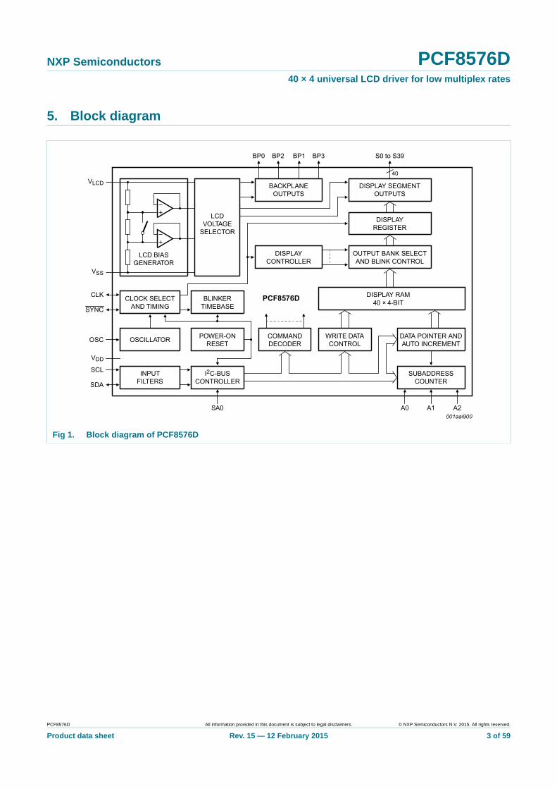
5. Block diagram
Fig 1. Block diagram of PCF8576D
PCF8576D All information provided in this document is subject to legal disclaimers. © NXP Semiconductors N.V. 2015. All rights reserved.
Product data sheet Rev. 15 — 12 February 2015 3 of 59
NXP Semiconductors PCF8576D40 × 4 universal LCD driver for low multiplex rates
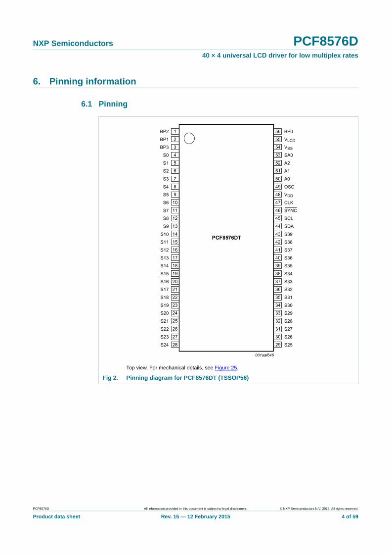
6. Pinning information
6.1 Pinning
Top view. For mechanical details, see Figure 25.
Fig 2. Pinning diagram for PCF8576DT (TSSOP56)
PCF8576D All information provided in this document is subject to legal disclaimers. © NXP Semiconductors N.V. 2015. All rights reserved.
Product data sheet Rev. 15 — 12 February 2015 4 of 59
NXP Semiconductors PCF8576D40 × 4 universal LCD driver for low multiplex rates
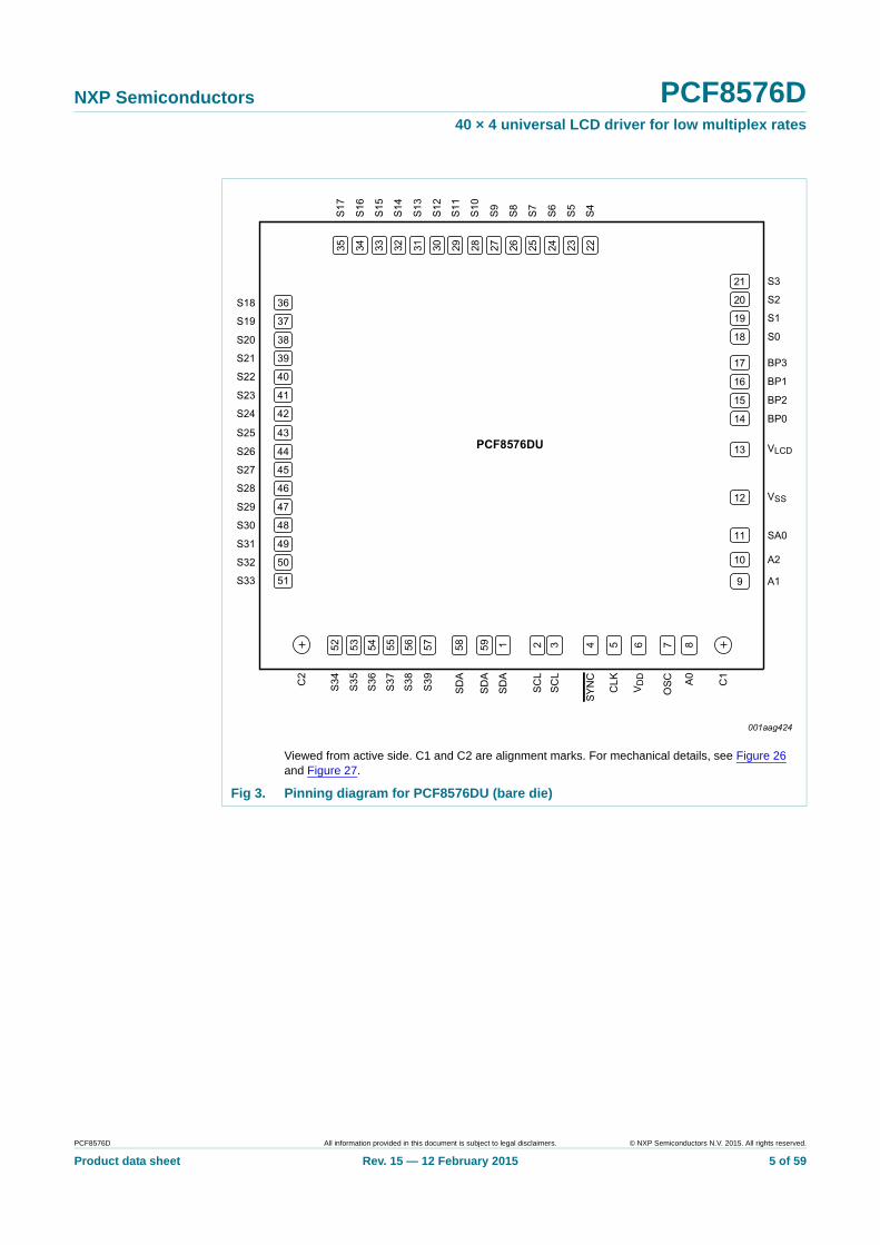
Viewed from active side. C1 and C2 are alignment marks. For mechanical details, see Figure 26 and Figure 27.
Fig 3. Pinning diagram for PCF8576DU (bare die)
PCF8576D All information provided in this document is subject to legal disclaimers. © NXP Semiconductors N.V. 2015. All rights reserved.
Product data sheet Rev. 15 — 12 February 2015 5 of 59
NXP Semiconductors PCF8576D40 × 4 universal LCD driver for low multiplex rates
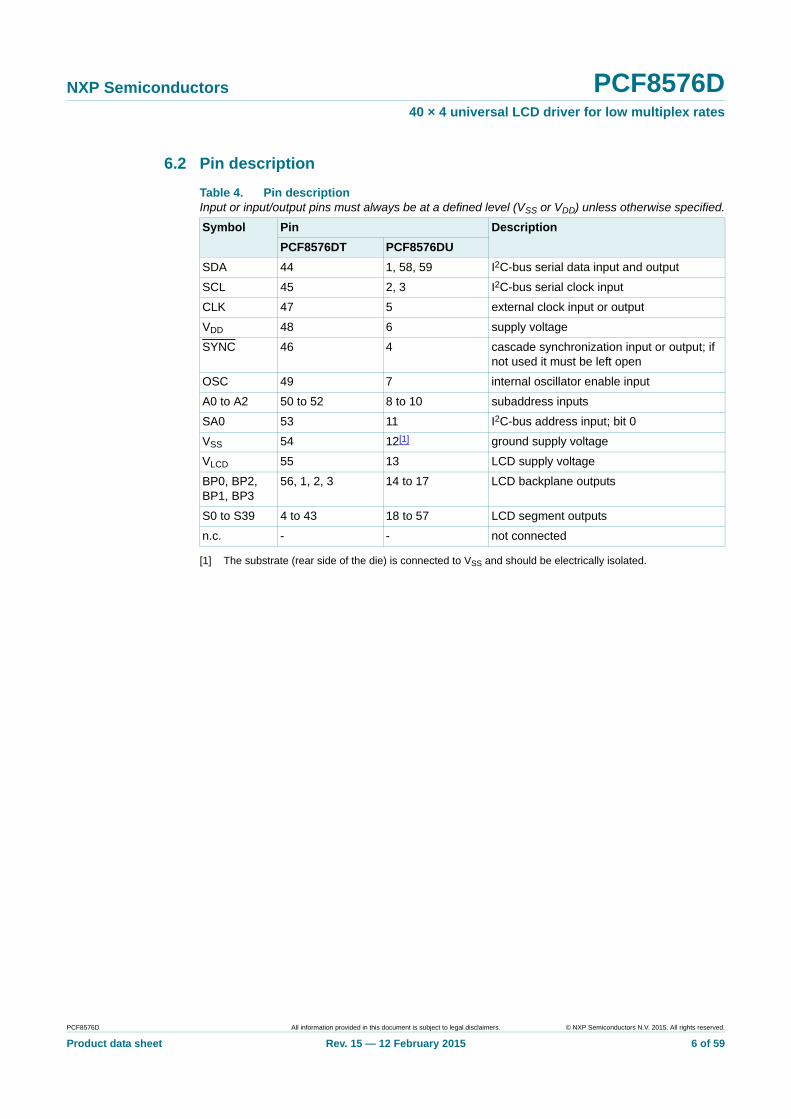
6.2 Pin description
[1] The substrate (rear side of the die) is connected to VSS and should be electrically isolated.
Table 4. Pin descriptionInput or input/output pins must always be at a defined level (VSS or VDD) unless otherwise specified.
Symbol Pin Description
PCF8576DT PCF8576DU
SDA 44 1, 58, 59 I2C-bus serial data input and output
SCL 45 2, 3 I2C-bus serial clock input
CLK 47 5 external clock input or output
VDD 48 6 supply voltage
SYNC 46 4 cascade synchronization input or output; if not used it must be left open
OSC 49 7 internal oscillator enable input
A0 to A2 50 to 52 8 to 10 subaddress inputs
SA0 53 11 I2C-bus address input; bit 0
VSS 54 12[1] ground supply voltage
VLCD 55 13 LCD supply voltage
BP0, BP2, BP1, BP3
56, 1, 2, 3 14 to 17 LCD backplane outputs
S0 to S39 4 to 43 18 to 57 LCD segment outputs
n.c. - - not connected
PCF8576D All information provided in this document is subject to legal disclaimers. © NXP Semiconductors N.V. 2015. All rights reserved.
Product data sheet Rev. 15 — 12 February 2015 6 of 59
NXP Semiconductors PCF8576D40 × 4 universal LCD driver for low multiplex rates
7. Functional description
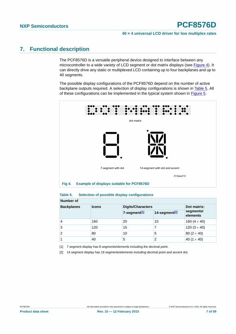
The PCF8576D is a versatile peripheral device designed to interface between any microcontroller to a wide variety of LCD segment or dot matrix displays (see Figure 4). It can directly drive any static or multiplexed LCD containing up to four backplanes and up to 40 segments.
The possible display configurations of the PCF8576D depend on the number of active backplane outputs required. A selection of display configurations is shown in Table 5. All of these configurations can be implemented in the typical system shown in Figure 5.
[1] 7 segment display has 8 segments/elements including the decimal point.
[2] 14 segment display has 16 segments/elements including decimal point and accent dot.
Fig 4. Example of displays suitable for PCF8576D
Table 5. Selection of possible display configurations
Number of
Backplanes Icons Digits/Characters Dot matrix:segments/ elements
7-segment[1] 14-segment[2]
4 160 20 10 160 (4 40)
3 120 15 7 120 (3 40)
2 80 10 5 80 (2 40)
1 40 5 2 40 (1 40)
PCF8576D All information provided in this document is subject to legal disclaimers. © NXP Semiconductors N.V. 2015. All rights reserved.
Product data sheet Rev. 15 — 12 February 2015 7 of 59
NXP Semiconductors PCF8576D40 × 4 universal LCD driver for low multiplex rates
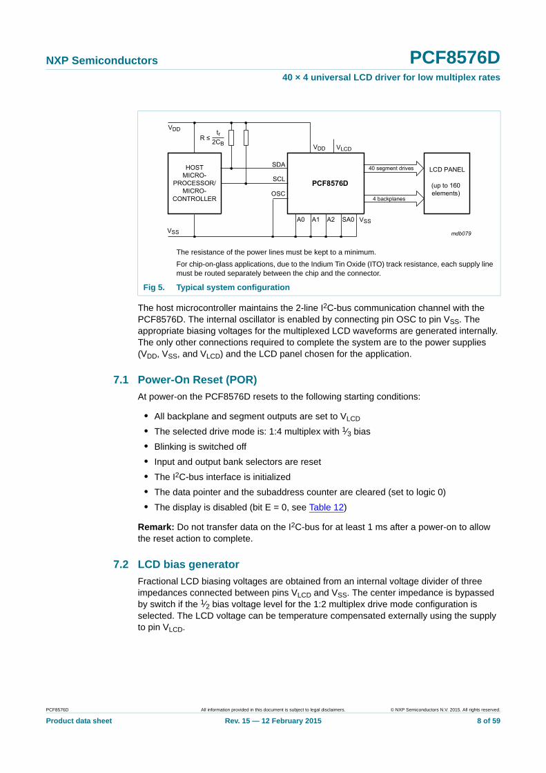
The host microcontroller maintains the 2-line I2C-bus communication channel with the PCF8576D. The internal oscillator is enabled by connecting pin OSC to pin VSS. The appropriate biasing voltages for the multiplexed LCD waveforms are generated internally. The only other connections required to complete the system are to the power supplies (VDD, VSS, and VLCD) and the LCD panel chosen for the application.
7.1 Power-On Reset (POR)
At power-on the PCF8576D resets to the following starting conditions:
• All backplane and segment outputs are set to VLCD
• The selected drive mode is: 1:4 multiplex with 1⁄3 bias
• Blinking is switched off
• Input and output bank selectors are reset
• The I2C-bus interface is initialized
• The data pointer and the subaddress counter are cleared (set to logic 0)
• The display is disabled (bit E = 0, see Table 12)
Remark: Do not transfer data on the I2C-bus for at least 1 ms after a power-on to allow the reset action to complete.
7.2 LCD bias generator
Fractional LCD biasing voltages are obtained from an internal voltage divider of three impedances connected between pins VLCD and VSS. The center impedance is bypassed by switch if the 1⁄2 bias voltage level for the 1:2 multiplex drive mode configuration is selected. The LCD voltage can be temperature compensated externally using the supply to pin VLCD.
The resistance of the power lines must be kept to a minimum.
For chip-on-glass applications, due to the Indium Tin Oxide (ITO) track resistance, each supply line must be routed separately between the chip and the connector.
Fig 5. Typical system configuration
PCF8576D All information provided in this document is subject to legal disclaimers. © NXP Semiconductors N.V. 2015. All rights reserved.
Product data sheet Rev. 15 — 12 February 2015 8 of 59
NXP Semiconductors PCF8576D40 × 4 universal LCD driver for low multiplex rates
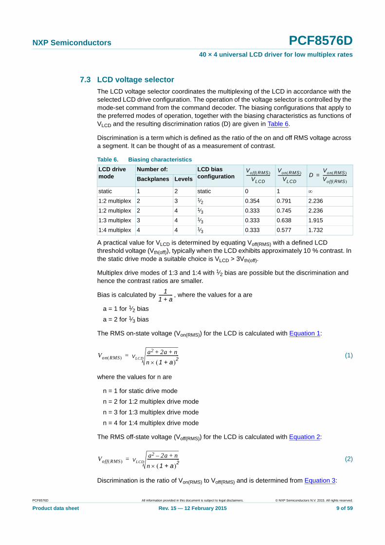
7.3 LCD voltage selector
The LCD voltage selector coordinates the multiplexing of the LCD in accordance with the selected LCD drive configuration. The operation of the voltage selector is controlled by the mode-set command from the command decoder. The biasing configurations that apply to the preferred modes of operation, together with the biasing characteristics as functions of VLCD and the resulting discrimination ratios (D) are given in Table 6.
Discrimination is a term which is defined as the ratio of the on and off RMS voltage across a segment. It can be thought of as a measurement of contrast.
A practical value for VLCD is determined by equating Voff(RMS) with a defined LCD threshold voltage (Vth(off)), typically when the LCD exhibits approximately 10 % contrast. In the static drive mode a suitable choice is VLCD > 3Vth(off).
Multiplex drive modes of 1:3 and 1:4 with 1⁄2 bias are possible but the discrimination and hence the contrast ratios are smaller.
Bias is calculated by , where the values for a are
a = 1 for 1⁄2 bias
a = 2 for 1⁄3 bias
The RMS on-state voltage (Von(RMS)) for the LCD is calculated with Equation 1:
(1)
where the values for n are
n = 1 for static drive mode
n = 2 for 1:2 multiplex drive mode
n = 3 for 1:3 multiplex drive mode
n = 4 for 1:4 multiplex drive mode
The RMS off-state voltage (Voff(RMS)) for the LCD is calculated with Equation 2:
(2)
Discrimination is the ratio of Von(RMS) to Voff(RMS) and is determined from Equation 3:
Table 6. Biasing characteristics
LCD drive mode
Number of: LCD bias configurationBackplanes Levels
static 1 2 static 0 1
1:2 multiplex 2 3 1⁄2 0.354 0.791 2.236
1:2 multiplex 2 4 1⁄3 0.333 0.745 2.236
1:3 multiplex 3 4 1⁄3 0.333 0.638 1.915
1:4 multiplex 4 4 1⁄3 0.333 0.577 1.732
Voff RMS VLCD
-------------------------Von RMS
VLCD------------------------ D
Von RMS Voff RMS -------------------------=
11 a+-------------
Von RMS a2 2a n+ +
n 1 a+ 2------------------------------VLCD
=
Voff RMS a2 2a– n+
n 1 a+ 2------------------------------VLCD
=
PCF8576D All information provided in this document is subject to legal disclaimers. © NXP Semiconductors N.V. 2015. All rights reserved.
Product data sheet Rev. 15 — 12 February 2015 9 of 59
NXP Semiconductors PCF8576D40 × 4 universal LCD driver for low multiplex rates
(3)
Using Equation 3, the discrimination for an LCD drive mode of 1:3 multiplex with 1⁄2 bias is and the discrimination for an LCD drive mode of 1:4 multiplex with
1⁄2 bias is .
The advantage of these LCD drive modes is a reduction of the LCD full scale voltage VLCD as follows:
• 1:3 multiplex (1⁄2 bias):
• 1:4 multiplex (1⁄2 bias):
These compare with when 1⁄3 bias is used.
It should be noted that VLCD is sometimes referred as the LCD operating voltage.
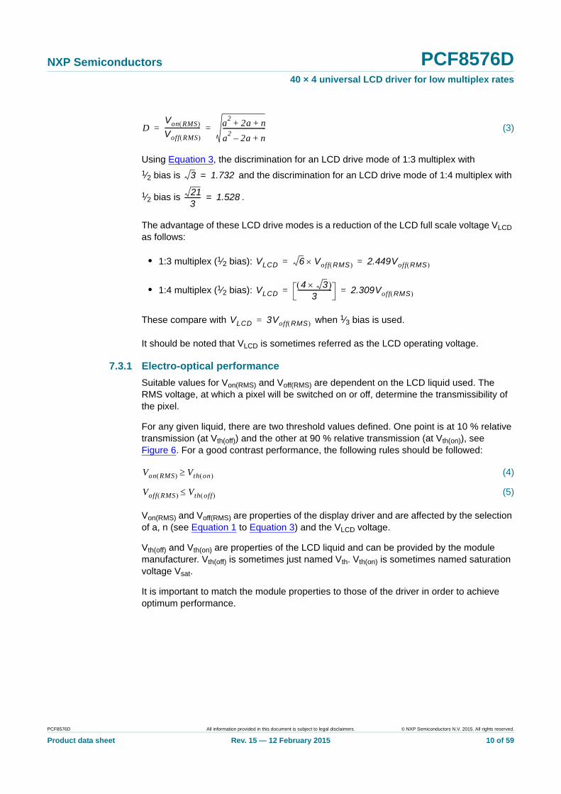
7.3.1 Electro-optical performance
Suitable values for Von(RMS) and Voff(RMS) are dependent on the LCD liquid used. The RMS voltage, at which a pixel will be switched on or off, determine the transmissibility of the pixel.
For any given liquid, there are two threshold values defined. One point is at 10 % relative transmission (at Vth(off)) and the other at 90 % relative transmission (at Vth(on)), see Figure 6. For a good contrast performance, the following rules should be followed:
(4)
(5)
Von(RMS) and Voff(RMS) are properties of the display driver and are affected by the selection of a, n (see Equation 1 to Equation 3) and the VLCD voltage.
Vth(off) and Vth(on) are properties of the LCD liquid and can be provided by the module manufacturer. Vth(off) is sometimes just named Vth. Vth(on) is sometimes named saturation voltage Vsat.
It is important to match the module properties to those of the driver in order to achieve optimum performance.
DVon RMS
Voff RMS ----------------------- a
22a n+ +
a2
2a– n+---------------------------= =
3 1.732=
213
---------- 1.528=
VLCD 6 Voff RMS 2.449Voff RMS = =
VLCD4 3
3---------------------- 2.309Voff RMS = =
VLCD 3Voff RMS =
Von RMS Vth on
Voff RMS Vth off
PCF8576D All information provided in this document is subject to legal disclaimers. © NXP Semiconductors N.V. 2015. All rights reserved.
Product data sheet Rev. 15 — 12 February 2015 10 of 59
NXP Semiconductors PCF8576D40 × 4 universal LCD driver for low multiplex rates
Fig 6. Electro-optical characteristic: relative transmission curve of the liquid
PCF8576D All information provided in this document is subject to legal disclaimers. © NXP Semiconductors N.V. 2015. All rights reserved.
Product data sheet Rev. 15 — 12 February 2015 11 of 59
NXP Semiconductors PCF8576D40 × 4 universal LCD driver for low multiplex rates
7.4 LCD drive mode waveforms
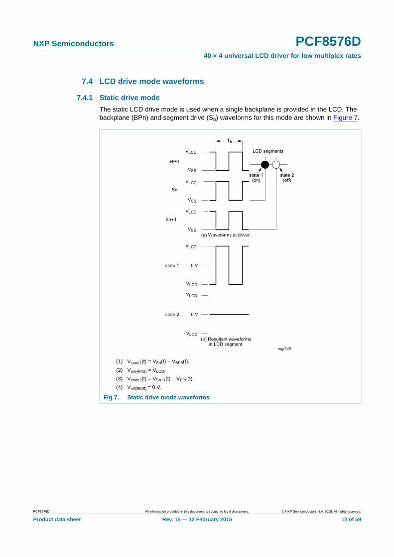
7.4.1 Static drive mode
The static LCD drive mode is used when a single backplane is provided in the LCD. The backplane (BPn) and segment drive (Sn) waveforms for this mode are shown in Figure 7.
(1) Vstate1(t) = VSn(t) VBP0(t).
(2) Von(RMS) = VLCD.
(3) Vstate2(t) = VSn+1(t) VBP0(t).
(4) Voff(RMS) = 0 V.
Fig 7. Static drive mode waveforms
PCF8576D All information provided in this document is subject to legal disclaimers. © NXP Semiconductors N.V. 2015. All rights reserved.
Product data sheet Rev. 15 — 12 February 2015 12 of 59
NXP Semiconductors PCF8576D40 × 4 universal LCD driver for low multiplex rates
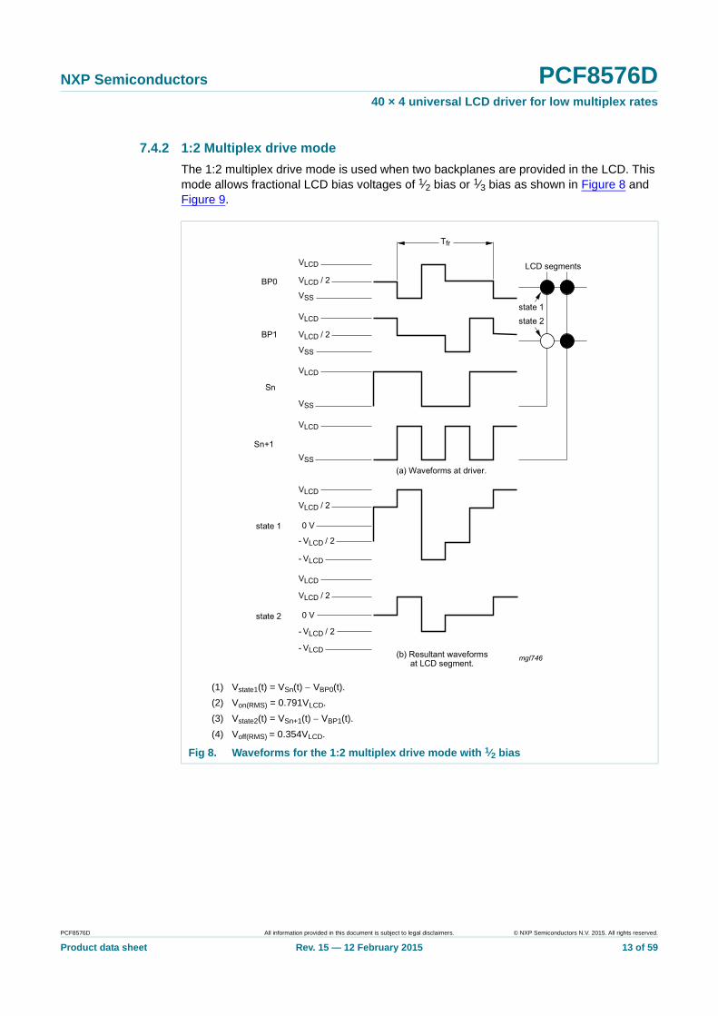
7.4.2 1:2 Multiplex drive mode
The 1:2 multiplex drive mode is used when two backplanes are provided in the LCD. This mode allows fractional LCD bias voltages of 1⁄2 bias or 1⁄3 bias as shown in Figure 8 and Figure 9.
(1) Vstate1(t) = VSn(t) VBP0(t).
(2) Von(RMS) = 0.791VLCD.
(3) Vstate2(t) = VSn+1(t) VBP1(t).
(4) Voff(RMS) = 0.354VLCD.
Fig 8. Waveforms for the 1:2 multiplex drive mode with 1⁄2 bias
PCF8576D All information provided in this document is subject to legal disclaimers. © NXP Semiconductors N.V. 2015. All rights reserved.
Product data sheet Rev. 15 — 12 February 2015 13 of 59
NXP Semiconductors PCF8576D40 × 4 universal LCD driver for low multiplex rates
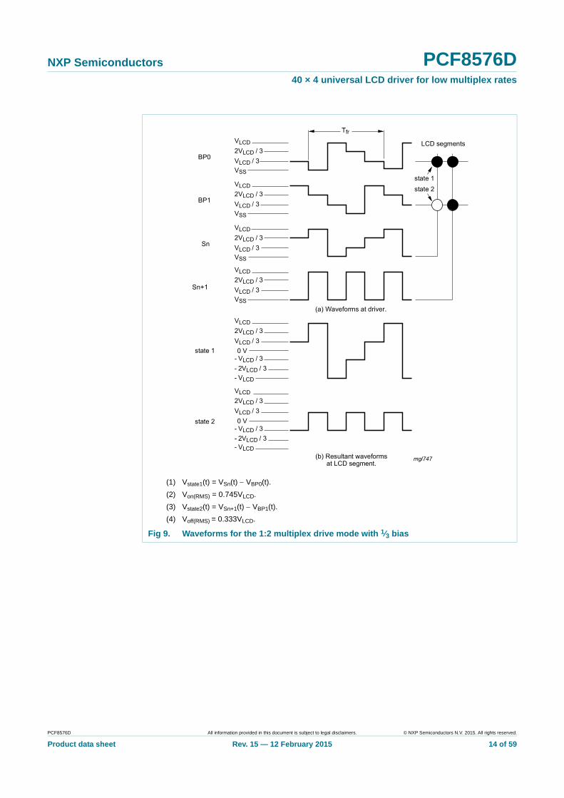
(1) Vstate1(t) = VSn(t) VBP0(t).
(2) Von(RMS) = 0.745VLCD.
(3) Vstate2(t) = VSn+1(t) VBP1(t).
(4) Voff(RMS) = 0.333VLCD.
Fig 9. Waveforms for the 1:2 multiplex drive mode with 1⁄3 bias
PCF8576D All information provided in this document is subject to legal disclaimers. © NXP Semiconductors N.V. 2015. All rights reserved.
Product data sheet Rev. 15 — 12 February 2015 14 of 59
NXP Semiconductors PCF8576D40 × 4 universal LCD driver for low multiplex rates
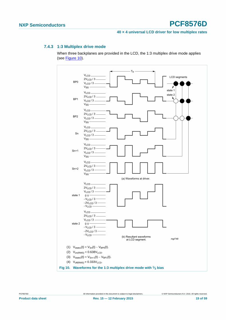
7.4.3 1:3 Multiplex drive mode
When three backplanes are provided in the LCD, the 1:3 multiplex drive mode applies (see Figure 10).
(1) Vstate1(t) = VSn(t) VBP0(t).
(2) Von(RMS) = 0.638VLCD.
(3) Vstate2(t) = VSn+1(t) VBP1(t).
(4) Voff(RMS) = 0.333VLCD.
Fig 10. Waveforms for the 1:3 multiplex drive mode with 1⁄3 bias
PCF8576D All information provided in this document is subject to legal disclaimers. © NXP Semiconductors N.V. 2015. All rights reserved.
Product data sheet Rev. 15 — 12 February 2015 15 of 59

NXP Semiconductors PCF8576D40 × 4 universal LCD driver for low multiplex rates
7.4.4 1:4 Multiplex drive mode
When four backplanes are provided in the LCD, the 1:4 multiplex drive mode applies (see Figure 11).
(1) Vstate1(t) = VSn(t) VBP0(t).
(2) Von(RMS) = 0.577VLCD.
(3) Vstate2(t) = VSn+1(t) VBP1(t).
(4) Voff(RMS) = 0.333VLCD.
Fig 11. Waveforms for the 1:4 multiplex drive mode with 1⁄3 bias
PCF8576D All information provided in this document is subject to legal disclaimers. © NXP Semiconductors N.V. 2015. All rights reserved.
Product data sheet Rev. 15 — 12 February 2015 16 of 59
NXP Semiconductors PCF8576D40 × 4 universal LCD driver for low multiplex rates
7.5 Oscillator
7.5.1 Internal clock
The internal logic of the PCF8576D and its LCD drive signals are timed either by its internal oscillator or by an external clock. The internal oscillator is enabled by connecting pin OSC to pin VSS. If the internal oscillator is used, the output from pin CLK can be used as the clock signal for several PCF8576Ds in the system that are connected in cascade.
7.5.2 External clock
Pin CLK is enabled as an external clock input by connecting pin OSC to VDD. The LCD frame signal frequency is determined by the clock frequency (fclk).
Remark: A clock signal must always be supplied to the device; removing the clock may freeze the LCD in a DC state, which is not suitable for the liquid crystal.
7.6 Timing
The PCF8576D timing controls the internal data flow of the device. This includes the transfer of display data from the display RAM to the display segment outputs. In cascaded applications, the correct timing relationship between each PCF8576D in the system is maintained by the synchronization signal at pin SYNC. The timing also generates the LCD frame signal whose frequency is derived from the clock frequency. The frame signal frequency is a fixed division of the clock frequency from either the internal or an external
clock: .
7.7 Display register
The display latch holds the display data while the corresponding multiplex signals are generated.
7.8 Segment outputs
The LCD drive section includes 40 segment outputs S0 to S39 which should be connected directly to the LCD. The segment output signals are generated in accordance with the multiplexed backplane signals and with data residing in the display latch. When less than 40 segment outputs are required, the unused segment outputs should be left open-circuit.
7.9 Backplane outputs
The LCD drive section includes four backplane outputs BP0 to BP3 which must be connected directly to the LCD. The backplane output signals are generated in accordance with the selected LCD drive mode. If less than four backplane outputs are required, the unused outputs can be left open-circuit.
ffrfclk
24-------=
PCF8576D All information provided in this document is subject to legal disclaimers. © NXP Semiconductors N.V. 2015. All rights reserved.
Product data sheet Rev. 15 — 12 February 2015 17 of 59
NXP Semiconductors PCF8576D40 × 4 universal LCD driver for low multiplex rates
• In 1:3 multiplex drive mode, BP3 carries the same signal as BP1, therefore these two adjacent outputs can be tied together to give enhanced drive capabilities.
• In 1:2 multiplex drive mode, BP0 and BP2, respectively, BP1 and BP3 all carry the same signals and may also be paired to increase the drive capabilities.
• In static drive mode the same signal is carried by all four backplane outputs and they can be connected in parallel for very high drive requirements.
7.10 Display RAM
The display RAM is a static 40 4-bit RAM which stores LCD data.
There is a one-to-one correspondence between
• the bits in the RAM bitmap and the LCD segments/elements
• the RAM columns and the segment outputs
• the RAM rows and the backplane outputs.
A logic 1 in the RAM bitmap indicates the on-state of the corresponding LCD element; similarly, a logic 0 indicates the off-state.
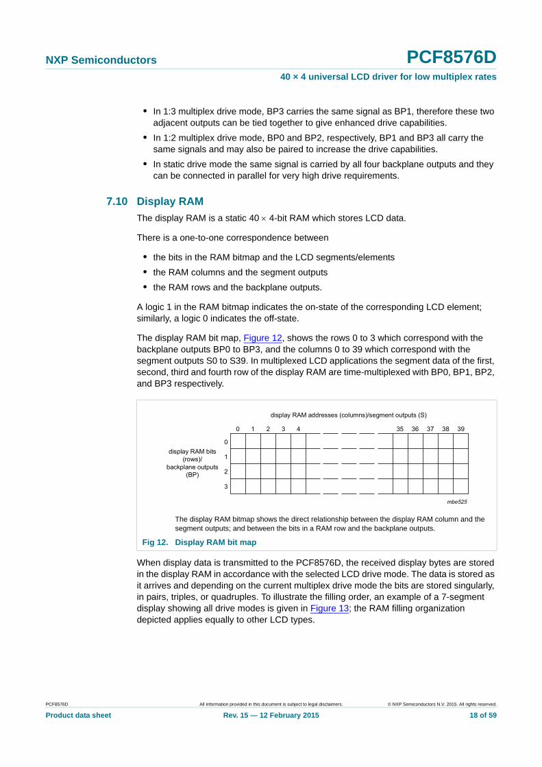
The display RAM bit map, Figure 12, shows the rows 0 to 3 which correspond with the backplane outputs BP0 to BP3, and the columns 0 to 39 which correspond with the segment outputs S0 to S39. In multiplexed LCD applications the segment data of the first, second, third and fourth row of the display RAM are time-multiplexed with BP0, BP1, BP2, and BP3 respectively.
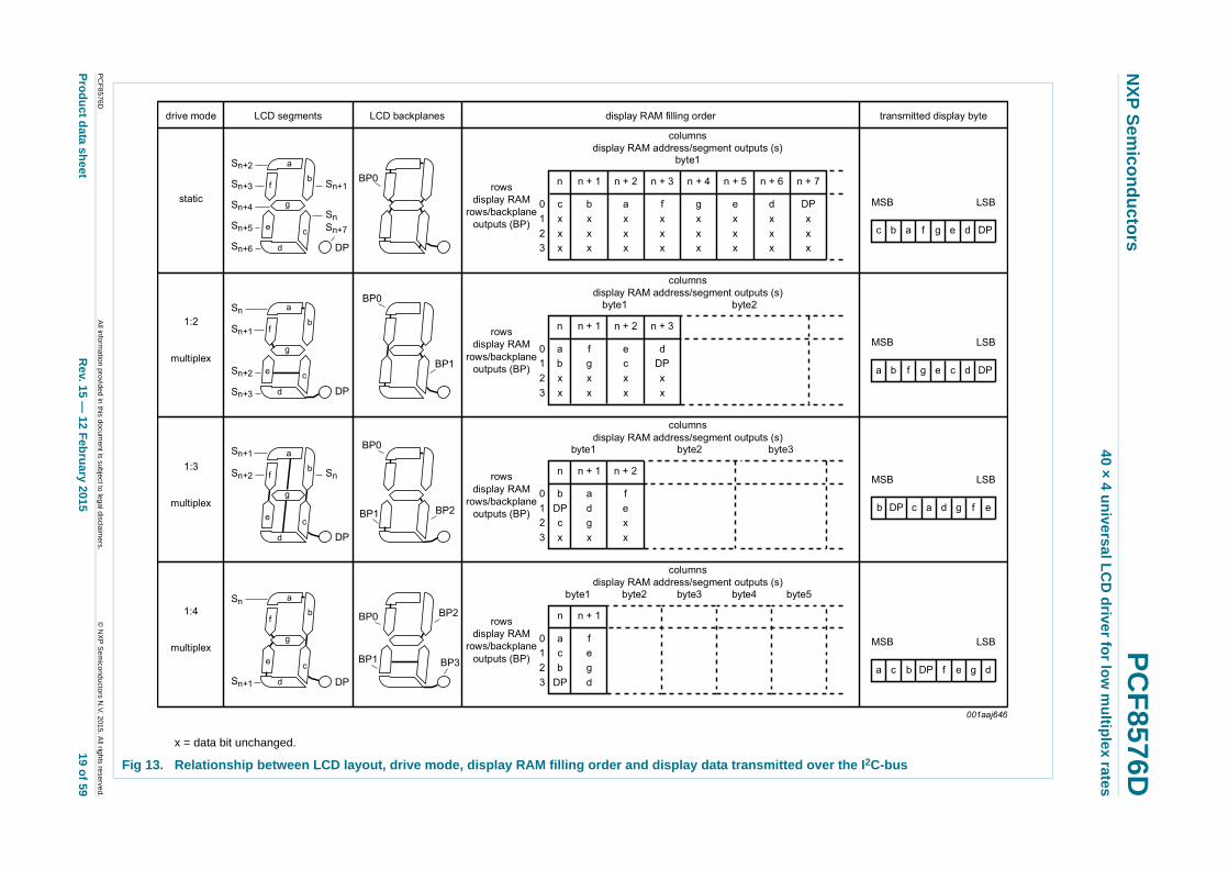
When display data is transmitted to the PCF8576D, the received display bytes are stored in the display RAM in accordance with the selected LCD drive mode. The data is stored as it arrives and depending on the current multiplex drive mode the bits are stored singularly, in pairs, triples, or quadruples. To illustrate the filling order, an example of a 7-segment display showing all drive modes is given in Figure 13; the RAM filling organization depicted applies equally to other LCD types.
The display RAM bitmap shows the direct relationship between the display RAM column and the segment outputs; and between the bits in a RAM row and the backplane outputs.
Fig 12. Display RAM bit map
PCF8576D All information provided in this document is subject to legal disclaimers. © NXP Semiconductors N.V. 2015. All rights reserved.
Product data sheet Rev. 15 — 12 February 2015 18 of 59
xxxxxxxxxxxxxxxxxxxxx xxxxxxxxxxxxxxxxxxxxxxxxxx xxxxxxx x x x xxxxxxxxxxxxxxxxxxxxxxxxxxxxxx xxxxxxxxxxxxxxxxxxx xx xx xxxxx xxxxxxxxxxxxxxxxxxxxxxxxxxx xxxxxxxxxxxxxxxxxxx xxxxxx xxxxxxxxxxxxxxxxxxxxxxxxxxxxxxxxxxx xxxxxxxxxxxx x x xxxxxxxxxxxxxxxxxxxxx xxxxxxxxxxxxxxxxxxxxxxxxxxxxxx xxxxx xxxxxxxxxxxxxxxxxxxxxxxxxxxxxxxxxxxxxxxxxxxxxxxxxx xxxxxxxx xxxxxxxxxxxxxxxxxxxxxxxxx xxxxxxxxxxxxxxxxxxxx xxx
PC
F85
76D
Pro
du
ct data sh
NX
P S
emico
nd
ucto
rsP
CF
8576D4
0 ×
4 u
niv
ers
al L
CD
drive
r for lo
w m
ultip
lex
rates
ver the I2C-bus
All inform
ation provided
in this docum
ent is subject to leg
al disclaim
ers.©
NX
P S
em
iconductors N
.V. 2015. A
ll rights re
served.
eetR
ev. 15 — 12 F
ebru
ary 2015
19 of 59
x = data bit unchanged.
Fig 13. Relationship between LCD layout, drive mode, display RAM filling order and display data transmitted o
NXP Semiconductors PCF8576D40 × 4 universal LCD driver for low multiplex rates
The following applies to Figure 13:
• In static drive mode the eight transmitted data bits are placed into row 0 as one byte.
• In 1:2 multiplex drive mode the eight transmitted data bits are placed in pairs into row 0 and 1 as four successive 2-bit RAM words.
• In 1:3 multiplex drive mode the eight bits are placed in triples into row 0, 1, and 2 as three successive 3-bit RAM words, with bit 3 of the third address left unchanged. It is not recommended to use this bit in a display because of the difficult addressing. This last bit may, if necessary, be controlled by an additional transfer to this address, but care should be taken to avoid overwriting adjacent data because always full bytes are transmitted (see Section 7.10.3).
• In 1:4 multiplex drive mode, the eight transmitted data bits are placed in quadruples into row 0, 1, 2, and 3 as two successive 4-bit RAM words.
7.10.1 Data pointer
The addressing mechanism for the display RAM is realized using the data pointer. This allows the loading of an individual display data byte, or a series of display data bytes, into any location of the display RAM. The sequence commences with the initialization of the data pointer by the load-data-pointer command (see Table 13). Following this command, an arriving data byte is stored at the display RAM address indicated by the data pointer. The filling order is shown in Figure 13. After each byte is stored, the content of the data pointer is automatically incremented by a value dependent on the selected LCD drive mode:
• In static drive mode by eight.
• In 1:2 multiplex drive mode by four.
• In 1:3 multiplex drive mode by three.
• In 1:4 multiplex drive mode by two.
If an I2C-bus data access terminates early then the state of the data pointer is unknown. Consequently, the data pointer must be rewritten prior to further RAM accesses.
7.10.2 Subaddress counter
The storage of display data is determined by the contents of the subaddress counter. Storage is allowed only when the content of the subaddress counter match with the hardware subaddress applied to A0, A1, and A2. The subaddress counter value is defined by the device-select command (see Table 14). If the content of the subaddress counter and the hardware subaddress do not match then data storage is inhibited but the data pointer is incremented as if data storage had taken place. The subaddress counter is also incremented when the data pointer overflows.
The storage arrangements described lead to extremely efficient data loading in cascaded applications. When a series of display bytes are sent to the display RAM, automatic wrap-over to the next PCF8576D occurs when the last RAM address is exceeded. Subaddressing across device boundaries is successful even if the change to the next device in the cascade occurs within a transmitted character.
The hardware subaddress must not be changed while the device is being accessed on the I2C-bus interface.
PCF8576D All information provided in this document is subject to legal disclaimers. © NXP Semiconductors N.V. 2015. All rights reserved.
Product data sheet Rev. 15 — 12 February 2015 20 of 59
NXP Semiconductors PCF8576D40 × 4 universal LCD driver for low multiplex rates
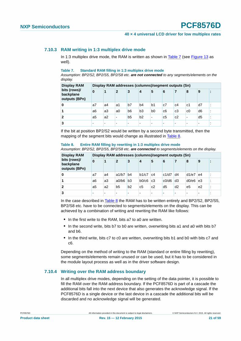
7.10.3 RAM writing in 1:3 multiplex drive mode
In 1:3 multiplex drive mode, the RAM is written as shown in Table 7 (see Figure 13 as well).
If the bit at position BP2/S2 would be written by a second byte transmitted, then the mapping of the segment bits would change as illustrated in Table 8.
In the case described in Table 8 the RAM has to be written entirely and BP2/S2, BP2/S5, BP2/S8 etc. have to be connected to segments/elements on the display. This can be achieved by a combination of writing and rewriting the RAM like follows:
• In the first write to the RAM, bits a7 to a0 are written.
• In the second write, bits b7 to b0 are written, overwriting bits a1 and a0 with bits b7 and b6.
• In the third write, bits c7 to c0 are written, overwriting bits b1 and b0 with bits c7 and c6.
Depending on the method of writing to the RAM (standard or entire filling by rewriting), some segments/elements remain unused or can be used, but it has to be considered in the module layout process as well as in the driver software design.
7.10.4 Writing over the RAM address boundary
In all multiplex drive modes, depending on the setting of the data pointer, it is possible to fill the RAM over the RAM address boundary. If the PCF8576D is part of a cascade the additional bits fall into the next device that also generates the acknowledge signal. If the PCF8576D is a single device or the last device in a cascade the additional bits will be discarded and no acknowledge signal will be generated.
Table 7. Standard RAM filling in 1:3 multiplex drive modeAssumption: BP2/S2, BP2/S5, BP2/S8 etc. are not connected to any segments/elements on the display.
Display RAM bits (rows)/ backplane outputs (BPn)
Display RAM addresses (columns)/segment outputs (Sn)
0 1 2 3 4 5 6 7 8 9 :
0 a7 a4 a1 b7 b4 b1 c7 c4 c1 d7 :
1 a6 a3 a0 b6 b3 b0 c6 c3 c0 d6 :
2 a5 a2 - b5 b2 - c5 c2 - d5 :
3 - - - - - - - - - - :
Table 8. Entire RAM filling by rewriting in 1:3 multiplex drive modeAssumption: BP2/S2, BP2/S5, BP2/S8 etc. are connected to segments/elements on the display.
Display RAM bits (rows)/ backplane outputs (BPn)
Display RAM addresses (columns)/segment outputs (Sn)
0 1 2 3 4 5 6 7 8 9 :
0 a7 a4 a1/b7 b4 b1/c7 c4 c1/d7 d4 d1/e7 e4 :
1 a6 a3 a0/b6 b3 b0/c6 c3 c0/d6 d3 d0/e6 e3 :
2 a5 a2 b5 b2 c5 c2 d5 d2 e5 e2 :
3 - - - - - - - - - - :
PCF8576D All information provided in this document is subject to legal disclaimers. © NXP Semiconductors N.V. 2015. All rights reserved.
Product data sheet Rev. 15 — 12 February 2015 21 of 59
NXP Semiconductors PCF8576D40 × 4 universal LCD driver for low multiplex rates
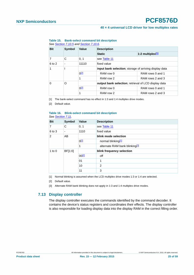
7.10.5 Output bank selector
The output bank selector (see Table 15) selects one of the four rows per display RAM address for transfer to the display register. The actual row selected depends on the selected LCD drive mode in operation and on the instant in the multiplex sequence.
• In 1:4 multiplex mode, all RAM addresses of row 0 are selected, these are followed by the contents of row 1, 2, and then 3
• In 1:3 multiplex mode, rows 0, 1, and 2 are selected sequentially
• In 1:2 multiplex mode, rows 0 and 1 are selected
• In static mode, row 0 is selected
The PCF8576D includes a RAM bank switching feature in the static and 1:2 multiplex drive modes. In the static drive mode, the bank-select command may request the contents of row 2 to be selected for display instead of the contents of row 0. In the 1:2 multiplex mode, the contents of rows 2 and 3 may be selected instead of rows 0 and 1. This gives the provision for preparing display information in an alternative bank and to be able to switch to it once it is assembled.
7.10.6 Input bank selector
The input bank selector loads display data into the display RAM in accordance with the selected LCD drive configuration. Display data can be loaded in row 2 in static drive mode or in rows 2 and 3 in 1:2 multiplex drive mode by using the bank-select command (see Table 15). The input bank selector functions independently to the output bank selector.
7.11 Blinking
The display blinking capabilities of the PCF8576D are very versatile. The whole display can blink at frequencies selected by the blink-select command (see Table 16). The blink frequencies are derived from the clock frequency. The ratio between the clock and blink frequencies depends on the blink mode selected (see Table 16).
An additional feature is for an arbitrary selection of LCD segments/elements to blink. This applies to the static and 1:2 multiplex drive modes and can be implemented without any communication overheads. By means of the output bank selector, the displayed RAM banks are exchanged with alternate RAM banks at the blink frequency. This mode can also be specified by the blink-select command.
In the 1:3 and 1:4 multiplex modes, where no alternative RAM bank is available, groups of LCD segments/elements can blink by selectively changing the display RAM data at fixed time intervals.
The entire display can blink at a frequency other than the nominal blink frequency. This can be effectively performed by resetting and setting the display enable bit E at the required rate using the mode-set command (see Table 12).
PCF8576D All information provided in this document is subject to legal disclaimers. © NXP Semiconductors N.V. 2015. All rights reserved.
Product data sheet Rev. 15 — 12 February 2015 22 of 59
NXP Semiconductors PCF8576D40 × 4 universal LCD driver for low multiplex rates
[1] Blink modes 1, 2 and 3 and the nominal blink frequencies 0.5 Hz, 1 Hz and 2 Hz correspond to an oscillator frequency (fclk) of 1536 Hz (see Section 13).
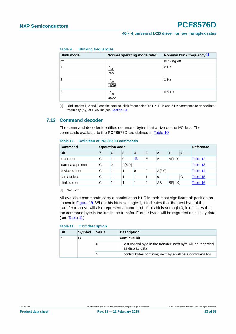
7.12 Command decoder
The command decoder identifies command bytes that arrive on the I2C-bus. The commands available to the PCF8576D are defined in Table 10.
[1] Not used.
All available commands carry a continuation bit C in their most significant bit position as shown in Figure 19. When this bit is set logic 1, it indicates that the next byte of the transfer to arrive will also represent a command. If this bit is set logic 0, it indicates that the command byte is the last in the transfer. Further bytes will be regarded as display data (see Table 11).
Table 9. Blinking frequencies
Blink mode Normal operating mode ratio Nominal blink frequency[1]
off - blinking off
1 2 Hz
2 1 Hz
3 0.5 Hz
fclk
768----------
fclk
1536-------------
fclk
3072-------------
Table 10. Definition of PCF8576D commands
Command Operation code Reference
Bit 7 6 5 4 3 2 1 0
mode-set C 1 0 -[1] E B M[1:0] Table 12
load-data-pointer C 0 P[5:0] Table 13
device-select C 1 1 0 0 A[2:0] Table 14
bank-select C 1 1 1 1 0 I O Table 15
blink-select C 1 1 1 0 AB BF[1:0] Table 16
Table 11. C bit description
Bit Symbol Value Description
7 C continue bit
0 last control byte in the transfer; next byte will be regarded as display data
1 control bytes continue; next byte will be a command too
PCF8576D All information provided in this document is subject to legal disclaimers. © NXP Semiconductors N.V. 2015. All rights reserved.
Product data sheet Rev. 15 — 12 February 2015 23 of 59
NXP Semiconductors PCF8576D40 × 4 universal LCD driver for low multiplex rates
[1] The possibility to disable the display allows implementation of blinking under external control.
[2] Default value.
[3] The display is disabled by setting all backplane and segment outputs to VLCD.
[4] Not applicable for static drive mode.
[1] Default value.
[1] Default value.
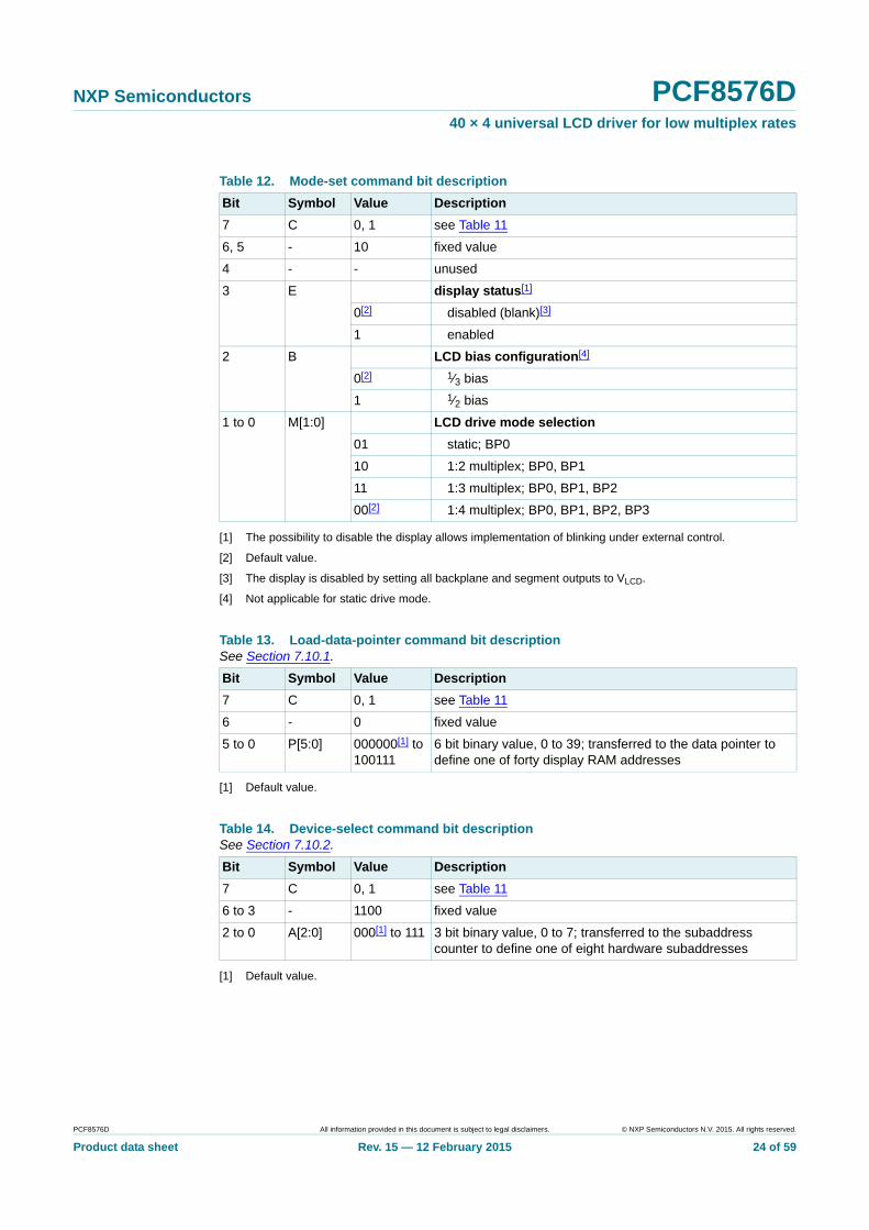
Table 12. Mode-set command bit description
Bit Symbol Value Description
7 C 0, 1 see Table 11
6, 5 - 10 fixed value
4 - - unused
3 E display status[1]
0[2] disabled (blank)[3]
1 enabled
2 B LCD bias configuration[4]
0[2] 1⁄3 bias
1 1⁄2 bias
1 to 0 M[1:0] LCD drive mode selection
01 static; BP0
10 1:2 multiplex; BP0, BP1
11 1:3 multiplex; BP0, BP1, BP2
00[2] 1:4 multiplex; BP0, BP1, BP2, BP3
Table 13. Load-data-pointer command bit descriptionSee Section 7.10.1.
Bit Symbol Value Description
7 C 0, 1 see Table 11
6 - 0 fixed value
5 to 0 P[5:0] 000000[1] to100111
6 bit binary value, 0 to 39; transferred to the data pointer to define one of forty display RAM addresses
Table 14. Device-select command bit descriptionSee Section 7.10.2.
Bit Symbol Value Description
7 C 0, 1 see Table 11
6 to 3 - 1100 fixed value
2 to 0 A[2:0] 000[1] to 111 3 bit binary value, 0 to 7; transferred to the subaddress counter to define one of eight hardware subaddresses
PCF8576D All information provided in this document is subject to legal disclaimers. © NXP Semiconductors N.V. 2015. All rights reserved.
Product data sheet Rev. 15 — 12 February 2015 24 of 59
NXP Semiconductors PCF8576D40 × 4 universal LCD driver for low multiplex rates
[1] The bank-select command has no effect in 1:3 and 1:4 multiplex drive modes.
[2] Default value.
[1] Normal blinking is assumed when the LCD multiplex drive modes 1:3 or 1:4 are selected.
[2] Default value.
[3] Alternate RAM bank blinking does not apply in 1:3 and 1:4 multiplex drive modes.
7.13 Display controller
The display controller executes the commands identified by the command decoder. It contains the device’s status registers and coordinates their effects. The display controller is also responsible for loading display data into the display RAM in the correct filling order.
Table 15. Bank-select command bit descriptionSee Section 7.10.5 and Section 7.10.6.
Bit Symbol Value Description
Static 1:2 multiplex[1]
7 C 0, 1 see Table 11
6 to 2 - 11110 fixed value
1 I input bank selection; storage of arriving display data
0[2] RAM row 0 RAM rows 0 and 1
1 RAM row 2 RAM rows 2 and 3
0 O output bank selection; retrieval of LCD display data
0[2] RAM row 0 RAM rows 0 and 1
1 RAM row 2 RAM rows 2 and 3
Table 16. Blink-select command bit descriptionSee Section 7.11.
Bit Symbol Value Description
7 C 0, 1 see Table 11
6 to 3 - 1110 fixed value
2 AB blink mode selection
0[2] normal blinking[1]
1 alternate RAM bank blinking[3]
1 to 0 BF[1:0] blink frequency selection
00[2] off
01 1
10 2
11 3
PCF8576D All information provided in this document is subject to legal disclaimers. © NXP Semiconductors N.V. 2015. All rights reserved.
Product data sheet Rev. 15 — 12 February 2015 25 of 59
NXP Semiconductors PCF8576D40 × 4 universal LCD driver for low multiplex rates
8. Characteristics of the I2C-bus
The I2C-bus is for bidirectional, two-line communication between different ICs or modules. The two lines are a Serial DAta line (SDA) and a Serial CLock line (SCL). Both lines must be connected to a positive supply via a pull-up resistor when connected to the output stages of a device. Data transfer may be initiated only when the bus is not busy.
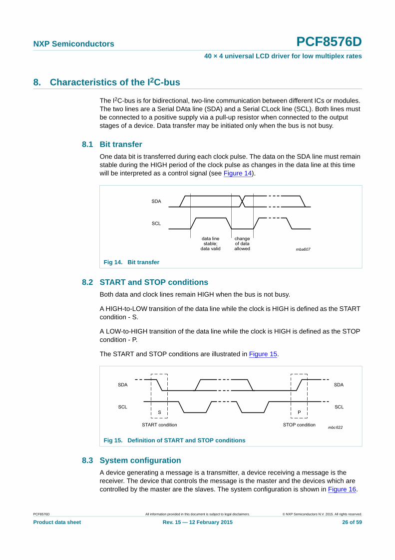
8.1 Bit transfer
One data bit is transferred during each clock pulse. The data on the SDA line must remain stable during the HIGH period of the clock pulse as changes in the data line at this time will be interpreted as a control signal (see Figure 14).
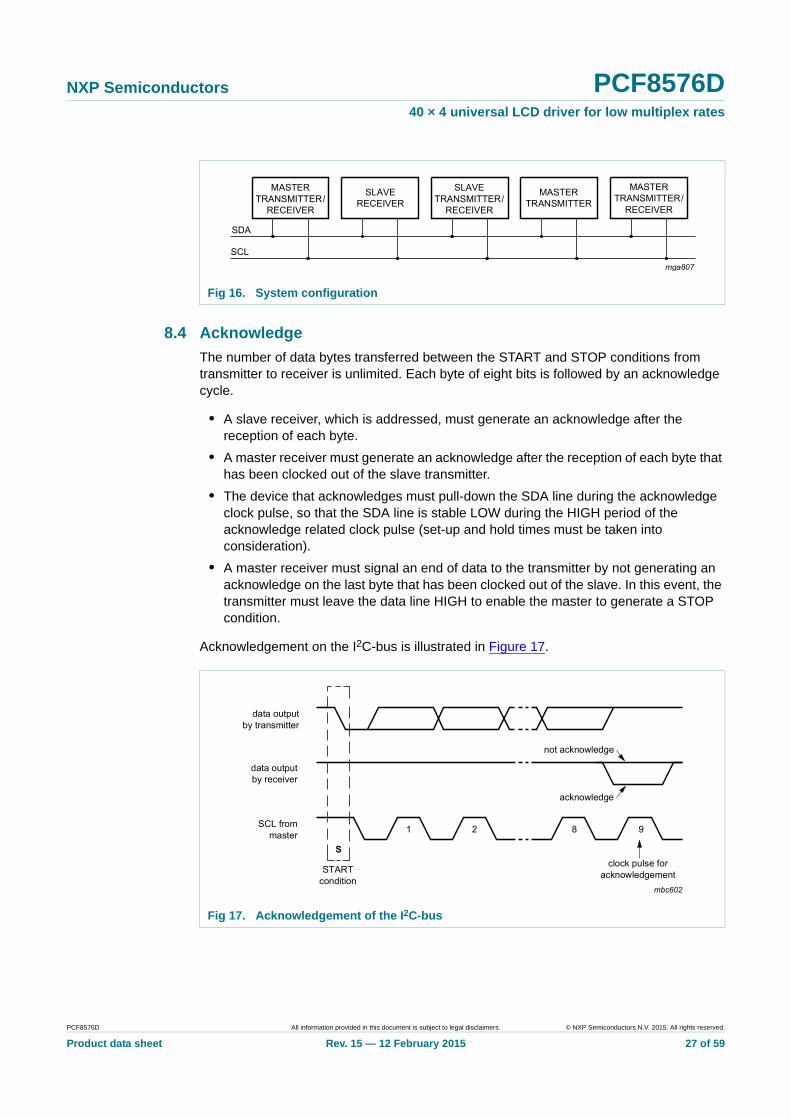
8.2 START and STOP conditions
Both data and clock lines remain HIGH when the bus is not busy.
A HIGH-to-LOW transition of the data line while the clock is HIGH is defined as the START condition - S.
A LOW-to-HIGH transition of the data line while the clock is HIGH is defined as the STOP condition - P.
The START and STOP conditions are illustrated in Figure 15.
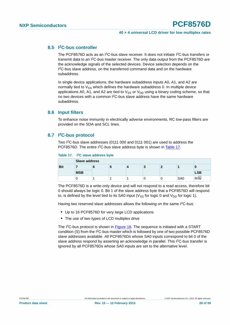
8.3 System configuration
A device generating a message is a transmitter, a device receiving a message is the receiver. The device that controls the message is the master and the devices which are controlled by the master are the slaves. The system configuration is shown in Figure 16.
Fig 14. Bit transfer
Fig 15. Definition of START and STOP conditions
PCF8576D All information provided in this document is subject to legal disclaimers. © NXP Semiconductors N.V. 2015. All rights reserved.
Product data sheet Rev. 15 — 12 February 2015 26 of 59
NXP Semiconductors PCF8576D40 × 4 universal LCD driver for low multiplex rates
8.4 Acknowledge
The number of data bytes transferred between the START and STOP conditions from transmitter to receiver is unlimited. Each byte of eight bits is followed by an acknowledge cycle.
• A slave receiver, which is addressed, must generate an acknowledge after the reception of each byte.
• A master receiver must generate an acknowledge after the reception of each byte that has been clocked out of the slave transmitter.
• The device that acknowledges must pull-down the SDA line during the acknowledge clock pulse, so that the SDA line is stable LOW during the HIGH period of the acknowledge related clock pulse (set-up and hold times must be taken into consideration).
• A master receiver must signal an end of data to the transmitter by not generating an acknowledge on the last byte that has been clocked out of the slave. In this event, the transmitter must leave the data line HIGH to enable the master to generate a STOP condition.
Acknowledgement on the I2C-bus is illustrated in Figure 17.
Fig 16. System configuration
Fig 17. Acknowledgement of the I2C-bus
PCF8576D All information provided in this document is subject to legal disclaimers. © NXP Semiconductors N.V. 2015. All rights reserved.
Product data sheet Rev. 15 — 12 February 2015 27 of 59
NXP Semiconductors PCF8576D40 × 4 universal LCD driver for low multiplex rates
8.5 I2C-bus controller
The PCF8576D acts as an I2C-bus slave receiver. It does not initiate I2C-bus transfers or transmit data to an I2C-bus master receiver. The only data output from the PCF8576D are the acknowledge signals of the selected devices. Device selection depends on the I2C-bus slave address, on the transferred command data and on the hardware subaddress.
In single device applications, the hardware subaddress inputs A0, A1, and A2 are normally tied to VSS which defines the hardware subaddress 0. In multiple device applications A0, A1, and A2 are tied to VSS or VDD using a binary coding scheme, so that no two devices with a common I2C-bus slave address have the same hardware subaddress.
8.6 Input filters
To enhance noise immunity in electrically adverse environments, RC low-pass filters are provided on the SDA and SCL lines.
8.7 I2C-bus protocol
Two I2C-bus slave addresses (0111 000 and 0111 001) are used to address the PCF8576D. The entire I2C-bus slave address byte is shown in Table 17.
The PCF8576D is a write-only device and will not respond to a read access, therefore bit 0 should always be logic 0. Bit 1 of the slave address byte that a PCF8576D will respond to, is defined by the level tied to its SA0 input (VSS for logic 0 and VDD for logic 1).
Having two reserved slave addresses allows the following on the same I2C-bus:
• Up to 16 PCF8576D for very large LCD applications
• The use of two types of LCD multiplex drive
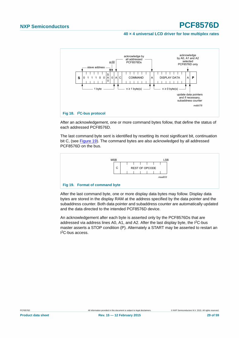
The I2C-bus protocol is shown in Figure 18. The sequence is initiated with a START condition (S) from the I2C-bus master which is followed by one of two possible PCF8576D slave addresses available. All PCF8576Ds whose SA0 inputs correspond to bit 0 of the slave address respond by asserting an acknowledge in parallel. This I2C-bus transfer is ignored by all PCF8576Ds whose SA0 inputs are set to the alternative level.
Table 17. I2C slave address byte
Slave address
Bit 7 6 5 4 3 2 1 0
MSB LSB
0 1 1 1 0 0 SA0 R/W
PCF8576D All information provided in this document is subject to legal disclaimers. © NXP Semiconductors N.V. 2015. All rights reserved.
Product data sheet Rev. 15 — 12 February 2015 28 of 59
NXP Semiconductors PCF8576D40 × 4 universal LCD driver for low multiplex rates
After an acknowledgement, one or more command bytes follow, that define the status of each addressed PCF8576D.
The last command byte sent is identified by resetting its most significant bit, continuation bit C, (see Figure 19). The command bytes are also acknowledged by all addressed PCF8576D on the bus.
After the last command byte, one or more display data bytes may follow. Display data bytes are stored in the display RAM at the address specified by the data pointer and the subaddress counter. Both data pointer and subaddress counter are automatically updated and the data directed to the intended PCF8576D device.
An acknowledgement after each byte is asserted only by the PCF8576Ds that are addressed via address lines A0, A1, and A2. After the last display byte, the I2C-bus master asserts a STOP condition (P). Alternately a START may be asserted to restart an I2C-bus access.
Fig 18. I2C-bus protocol
Fig 19. Format of command byte
PCF8576D All information provided in this document is subject to legal disclaimers. © NXP Semiconductors N.V. 2015. All rights reserved.
Product data sheet Rev. 15 — 12 February 2015 29 of 59
NXP Semiconductors PCF8576D40 × 4 universal LCD driver for low multiplex rates
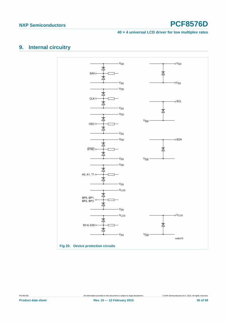
9. Internal circuitry
Fig 20. Device protection circuits
PCF8576D All information provided in this document is subject to legal disclaimers. © NXP Semiconductors N.V. 2015. All rights reserved.
Product data sheet Rev. 15 — 12 February 2015 30 of 59
NXP Semiconductors PCF8576D40 × 4 universal LCD driver for low multiplex rates
10. Safety notes
CAUTION
This device is sensitive to ElectroStatic Discharge (ESD). Observe precautions for handling electrostatic sensitive devices.
Such precautions are described in the ANSI/ESD S20.20, IEC/ST 61340-5, JESD625-A or equivalent standards.
CAUTION
Static voltages across the liquid crystal display can build up when the LCD supply voltage (VLCD) is on while the IC supply voltage (VDD) is off, or vice versa. This may cause unwanted display artifacts. To avoid such artifacts, VLCD and VDD must be applied or removed together.
CAUTION
Semiconductors are light sensitive. Exposure to light sources can cause the IC to malfunction. The IC must be protected against light. The protection must be applied to all sides of the IC.
PCF8576D All information provided in this document is subject to legal disclaimers. © NXP Semiconductors N.V. 2015. All rights reserved.
Product data sheet Rev. 15 — 12 February 2015 31 of 59
NXP Semiconductors PCF8576D40 × 4 universal LCD driver for low multiplex rates
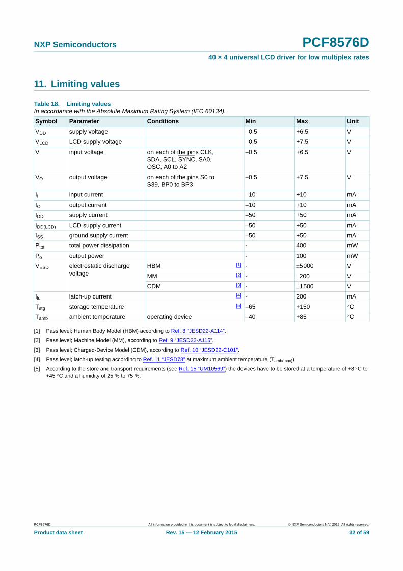
11. Limiting values
[1] Pass level; Human Body Model (HBM) according to Ref. 8 “JESD22-A114”.
[2] Pass level; Machine Model (MM), according to Ref. 9 “JESD22-A115”.
[3] Pass level; Charged-Device Model (CDM), according to Ref. 10 “JESD22-C101”.
[4] Pass level; latch-up testing according to Ref. 11 “JESD78” at maximum ambient temperature (Tamb(max)).
[5] According to the store and transport requirements (see Ref. 15 “UM10569”) the devices have to be stored at a temperature of +8 C to +45 C and a humidity of 25 % to 75 %.
Table 18. Limiting valuesIn accordance with the Absolute Maximum Rating System (IEC 60134).
Symbol Parameter Conditions Min Max Unit
VDD supply voltage 0.5 +6.5 V
VLCD LCD supply voltage 0.5 +7.5 V
VI input voltage on each of the pins CLK, SDA, SCL, SYNC, SA0, OSC, A0 to A2
0.5 +6.5 V
VO output voltage on each of the pins S0 to S39, BP0 to BP3
0.5 +7.5 V
II input current 10 +10 mA
IO output current 10 +10 mA
IDD supply current 50 +50 mA
IDD(LCD) LCD supply current 50 +50 mA
ISS ground supply current 50 +50 mA
Ptot total power dissipation - 400 mW
Po output power - 100 mW
VESD electrostatic discharge voltage
HBM [1] - 5000 V
MM [2] - 200 V
CDM [3] - 1500 V
Ilu latch-up current [4] - 200 mA
Tstg storage temperature [5] 65 +150 C
Tamb ambient temperature operating device 40 +85 C
PCF8576D All information provided in this document is subject to legal disclaimers. © NXP Semiconductors N.V. 2015. All rights reserved.
Product data sheet Rev. 15 — 12 February 2015 32 of 59
NXP Semiconductors PCF8576D40 × 4 universal LCD driver for low multiplex rates
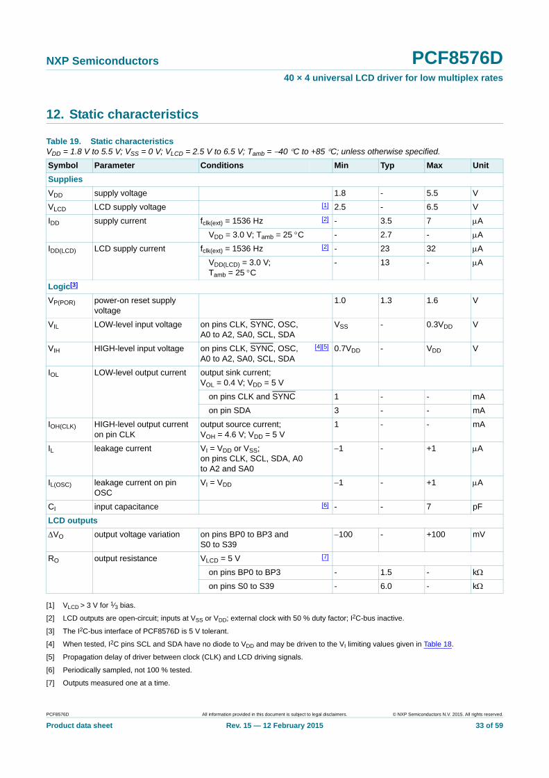
12. Static characteristics
[1] VLCD > 3 V for 1⁄3 bias.
[2] LCD outputs are open-circuit; inputs at VSS or VDD; external clock with 50 % duty factor; I2C-bus inactive.
[3] The I2C-bus interface of PCF8576D is 5 V tolerant.
[4] When tested, I2C pins SCL and SDA have no diode to VDD and may be driven to the VI limiting values given in Table 18.
[5] Propagation delay of driver between clock (CLK) and LCD driving signals.
[6] Periodically sampled, not 100 % tested.
[7] Outputs measured one at a time.
Table 19. Static characteristicsVDD = 1.8 V to 5.5 V; VSS = 0 V; VLCD = 2.5 V to 6.5 V; Tamb = 40 C to +85 C; unless otherwise specified.
Symbol Parameter Conditions Min Typ Max Unit
Supplies
VDD supply voltage 1.8 - 5.5 V
VLCD LCD supply voltage [1] 2.5 - 6.5 V
IDD supply current fclk(ext) = 1536 Hz [2] - 3.5 7 A
VDD = 3.0 V; Tamb = 25 C - 2.7 - A
IDD(LCD) LCD supply current fclk(ext) = 1536 Hz [2] - 23 32 A
VDD(LCD) = 3.0 V; Tamb = 25 C
- 13 - A
Logic[3]
VP(POR) power-on reset supply voltage
1.0 1.3 1.6 V
VIL LOW-level input voltage on pins CLK, SYNC, OSC, A0 to A2, SA0, SCL, SDA
VSS - 0.3VDD V
VIH HIGH-level input voltage on pins CLK, SYNC, OSC, A0 to A2, SA0, SCL, SDA
[4][5] 0.7VDD - VDD V
IOL LOW-level output current output sink current;VOL = 0.4 V; VDD = 5 V
on pins CLK and SYNC 1 - - mA
on pin SDA 3 - - mA
IOH(CLK) HIGH-level output current on pin CLK
output source current;VOH = 4.6 V; VDD = 5 V
1 - - mA
IL leakage current VI = VDD or VSS;on pins CLK, SCL, SDA, A0 to A2 and SA0
1 - +1 A
IL(OSC) leakage current on pin OSC
VI = VDD 1 - +1 A
CI input capacitance [6] - - 7 pF
LCD outputs
VO output voltage variation on pins BP0 to BP3 andS0 to S39
100 - +100 mV
RO output resistance VLCD = 5 V [7]
on pins BP0 to BP3 - 1.5 - k
on pins S0 to S39 - 6.0 - k
PCF8576D All information provided in this document is subject to legal disclaimers. © NXP Semiconductors N.V. 2015. All rights reserved.
Product data sheet Rev. 15 — 12 February 2015 33 of 59
NXP Semiconductors PCF8576D40 × 4 universal LCD driver for low multiplex rates
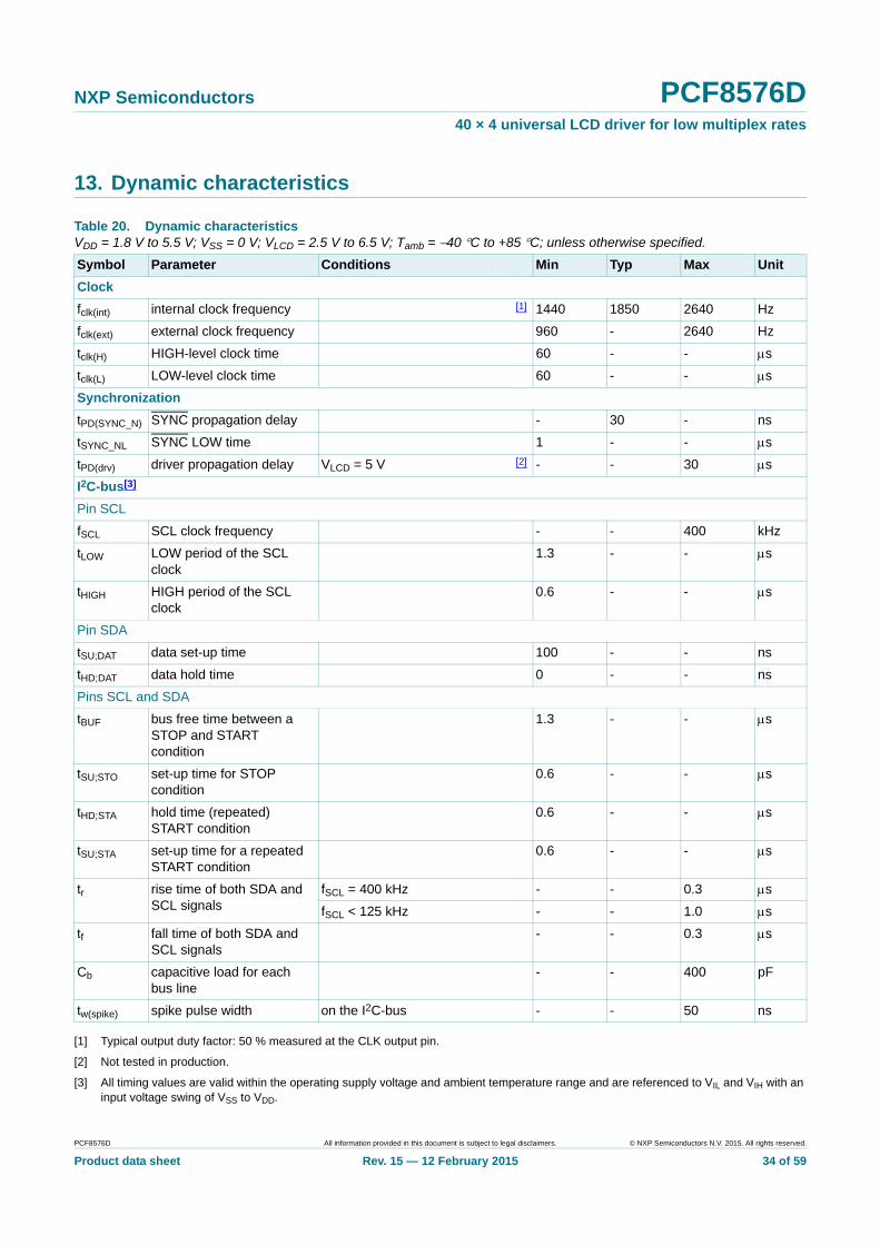
13. Dynamic characteristics
[1] Typical output duty factor: 50 % measured at the CLK output pin.
[2] Not tested in production.
[3] All timing values are valid within the operating supply voltage and ambient temperature range and are referenced to VIL and VIH with an input voltage swing of VSS to VDD.
Table 20. Dynamic characteristicsVDD = 1.8 V to 5.5 V; VSS = 0 V; VLCD = 2.5 V to 6.5 V; Tamb = 40 C to +85 C; unless otherwise specified.
Symbol Parameter Conditions Min Typ Max Unit
Clock
fclk(int) internal clock frequency [1] 1440 1850 2640 Hz
fclk(ext) external clock frequency 960 - 2640 Hz
tclk(H) HIGH-level clock time 60 - - s
tclk(L) LOW-level clock time 60 - - s
Synchronization
tPD(SYNC_N) SYNC propagation delay - 30 - ns
tSYNC_NL SYNC LOW time 1 - - s
tPD(drv) driver propagation delay VLCD = 5 V [2] - - 30 s
I2C-bus[3]
Pin SCL
fSCL SCL clock frequency - - 400 kHz
tLOW LOW period of the SCL clock
1.3 - - s
tHIGH HIGH period of the SCL clock
0.6 - - s
Pin SDA
tSU;DAT data set-up time 100 - - ns
tHD;DAT data hold time 0 - - ns
Pins SCL and SDA
tBUF bus free time between a STOP and START condition
1.3 - - s
tSU;STO set-up time for STOP condition
0.6 - - s
tHD;STA hold time (repeated) START condition
0.6 - - s
tSU;STA set-up time for a repeated START condition
0.6 - - s
tr rise time of both SDA and SCL signals
fSCL = 400 kHz - - 0.3 s
fSCL < 125 kHz - - 1.0 s
tf fall time of both SDA and SCL signals
- - 0.3 s
Cb capacitive load for each bus line
- - 400 pF
tw(spike) spike pulse width on the I2C-bus - - 50 ns
PCF8576D All information provided in this document is subject to legal disclaimers. © NXP Semiconductors N.V. 2015. All rights reserved.
Product data sheet Rev. 15 — 12 February 2015 34 of 59
NXP Semiconductors PCF8576D40 × 4 universal LCD driver for low multiplex rates
14. Application information
14.1 Cascaded operation
In large display configurations, up to 16 PCF8576Ds can be differentiated on the same I2C-bus by using the 3-bit hardware subaddresses (A0, A1 and A2) and the programmable I2C-bus slave address (SA0).
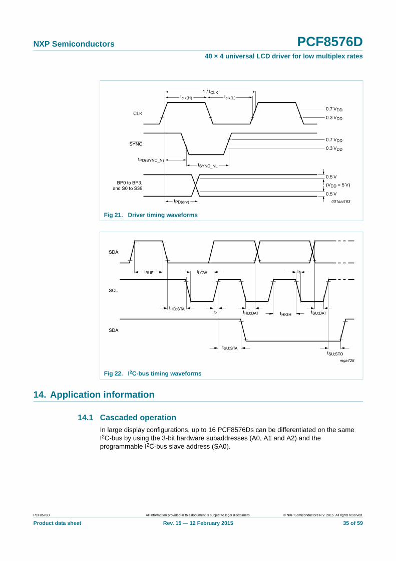
Fig 21. Driver timing waveforms
Fig 22. I2C-bus timing waveforms
PCF8576D All information provided in this document is subject to legal disclaimers. © NXP Semiconductors N.V. 2015. All rights reserved.
Product data sheet Rev. 15 — 12 February 2015 35 of 59
NXP Semiconductors PCF8576D40 × 4 universal LCD driver for low multiplex rates
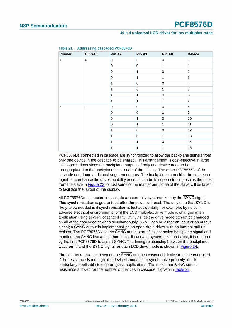
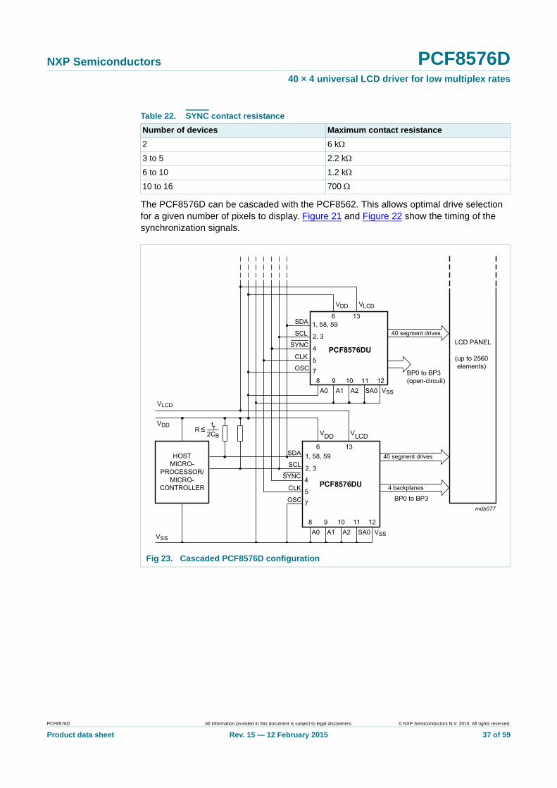
PCF8576Ds connected in cascade are synchronized to allow the backplane signals from only one device in the cascade to be shared. This arrangement is cost-effective in large LCD applications since the backplane outputs of only one device need to be through-plated to the backplane electrodes of the display. The other PCF8576D of the cascade contribute additional segment outputs. The backplanes can either be connected together to enhance the drive capability or some can be left open-circuit (such as the ones from the slave in Figure 23) or just some of the master and some of the slave will be taken to facilitate the layout of the display.
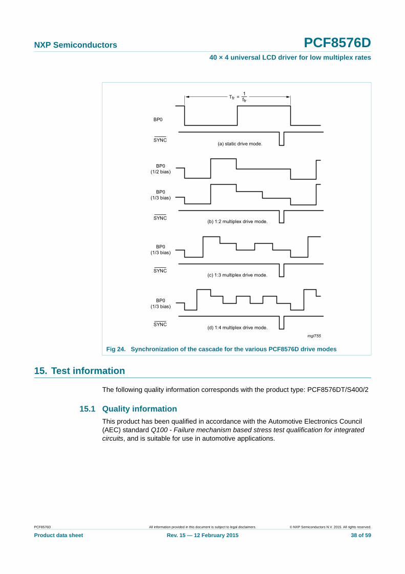
All PCF8576Ds connected in cascade are correctly synchronized by the SYNC signal. This synchronization is guaranteed after the power-on reset. The only time that SYNC is likely to be needed is if synchronization is lost accidentally, for example, by noise in adverse electrical environments, or if the LCD multiplex drive mode is changed in an application using several cascaded PCF8576Ds, as the drive mode cannot be changed on all of the cascaded devices simultaneously. SYNC can be either an input or an output signal; a SYNC output is implemented as an open-drain driver with an internal pull-up resistor. The PCF8576D asserts SYNC at the start of its last active backplane signal and monitors the SYNC line at all other times. If cascade synchronization is lost, it is restored by the first PCF8576D to assert SYNC. The timing relationship between the backplane waveforms and the SYNC signal for each LCD drive mode is shown in Figure 24.
The contact resistance between the SYNC on each cascaded device must be controlled. If the resistance is too high, the device is not able to synchronize properly; this is particularly applicable to chip-on-glass applications. The maximum SYNC contact resistance allowed for the number of devices in cascade is given in Table 22.
Table 21. Addressing cascaded PCF8576D
Cluster Bit SA0 Pin A2 Pin A1 Pin A0 Device
1 0 0 0 0 0
0 0 1 1
0 1 0 2
0 1 1 3
1 0 0 4
1 0 1 5
1 1 0 6
1 1 1 7
2 1 0 0 0 8
0 0 1 9
0 1 0 10
0 1 1 11
1 0 0 12
1 0 1 13
1 1 0 14
1 1 1 15
PCF8576D All information provided in this document is subject to legal disclaimers. © NXP Semiconductors N.V. 2015. All rights reserved.
Product data sheet Rev. 15 — 12 February 2015 36 of 59
NXP Semiconductors PCF8576D40 × 4 universal LCD driver for low multiplex rates
The PCF8576D can be cascaded with the PCF8562. This allows optimal drive selection for a given number of pixels to display. Figure 21 and Figure 22 show the timing of the synchronization signals.
Table 22. SYNC contact resistance
Number of devices Maximum contact resistance
2 6 k
3 to 5 2.2 k
6 to 10 1.2 k
10 to 16 700
Fig 23. Cascaded PCF8576D configuration
PCF8576D All information provided in this document is subject to legal disclaimers. © NXP Semiconductors N.V. 2015. All rights reserved.
Product data sheet Rev. 15 — 12 February 2015 37 of 59
NXP Semiconductors PCF8576D40 × 4 universal LCD driver for low multiplex rates
15. Test information
The following quality information corresponds with the product type: PCF8576DT/S400/2
15.1 Quality information
This product has been qualified in accordance with the Automotive Electronics Council (AEC) standard Q100 - Failure mechanism based stress test qualification for integrated circuits, and is suitable for use in automotive applications.
Fig 24. Synchronization of the cascade for the various PCF8576D drive modes
PCF8576D All information provided in this document is subject to legal disclaimers. © NXP Semiconductors N.V. 2015. All rights reserved.
Product data sheet Rev. 15 — 12 February 2015 38 of 59
NXP Semiconductors PCF8576D40 × 4 universal LCD driver for low multiplex rates
16. Package outline
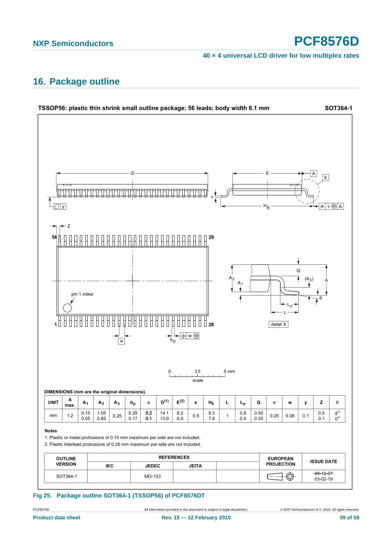
Fig 25. Package outline SOT364-1 (TSSOP56) of PCF8576DT
PCF8576D All information provided in this document is subject to legal disclaimers. © NXP Semiconductors N.V. 2015. All rights reserved.
Product data sheet Rev. 15 — 12 February 2015 39 of 59
NXP Semiconductors PCF8576D40 × 4 universal LCD driver for low multiplex rates
17. Bare die outline
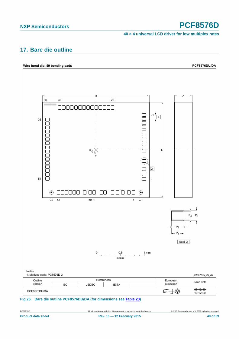
Fig 26. Bare die outline PCF8576DU/DA (for dimensions see Table 23)
PCF8576D All information provided in this document is subject to legal disclaimers. © NXP Semiconductors N.V. 2015. All rights reserved.
Product data sheet Rev. 15 — 12 February 2015 40 of 59
NXP Semiconductors PCF8576D40 × 4 universal LCD driver for low multiplex rates
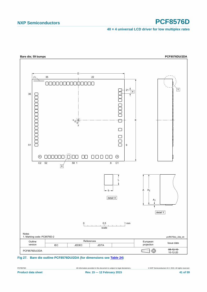
Fig 27. Bare die outline PCF8576DU/2DA (for dimensions see Table 24)
PCF8576D All information provided in this document is subject to legal disclaimers. © NXP Semiconductors N.V. 2015. All rights reserved.
Product data sheet Rev. 15 — 12 February 2015 41 of 59
NXP Semiconductors PCF8576D40 × 4 universal LCD driver for low multiplex rates
[1] Dimension not drawn to scale.
[2] Pad size.
[3] Passivation opening.
[1] Dimension not drawn to scale.
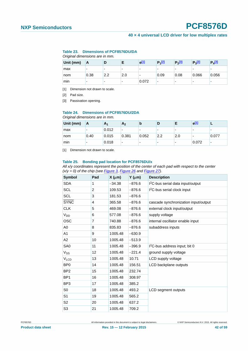
Table 23. Dimensions of PCF8576DU/DAOriginal dimensions are in mm.
Unit (mm) A D E e[1] P1[2] P2
[3] P3[2] P4
[3]
max - - - - - - - -
nom 0.38 2.2 2.0 - 0.09 0.08 0.066 0.056
min - - - 0.072 - - - -
Table 24. Dimensions of PCF8576DU/2DAOriginal dimensions are in mm.
Unit (mm) A A1 A2 b D E e[1] L
max - 0.012 - - - - - -
nom 0.40 0.015 0.381 0.052 2.2 2.0 - 0.077
min - 0.018 - - - - 0.072 -
Table 25. Bonding pad location for PCF8576DU/xAll x/y coordinates represent the position of the center of each pad with respect to the center (x/y = 0) of the chip (see Figure 3, Figure 26 and Figure 27).
Symbol Pad X (m) Y (m) Description
SDA 1 34.38 876.6 I2C-bus serial data input/output
SCL 2 109.53 876.6 I2C-bus serial clock input
SCL 3 181.53 876.6
SYNC 4 365.58 876.6 cascade synchronization input/output
CLK 5 469.08 876.6 external clock input/output
VDD 6 577.08 876.6 supply voltage
OSC 7 740.88 876.6 internal oscillator enable input
A0 8 835.83 876.6 subaddress inputs
A1 9 1005.48 630.9
A2 10 1005.48 513.9
SA0 11 1005.48 396.9 I2C-bus address input; bit 0
VSS 12 1005.48 221.4 ground supply voltage
VLCD 13 1005.48 10.71 LCD supply voltage
BP0 14 1005.48 156.51 LCD backplane outputs
BP2 15 1005.48 232.74
BP1 16 1005.48 308.97
BP3 17 1005.48 385.2
S0 18 1005.48 493.2 LCD segment outputs
S1 19 1005.48 565.2
S2 20 1005.48 637.2
S3 21 1005.48 709.2
PCF8576D All information provided in this document is subject to legal disclaimers. © NXP Semiconductors N.V. 2015. All rights reserved.
Product data sheet Rev. 15 — 12 February 2015 42 of 59
NXP Semiconductors PCF8576D40 × 4 universal LCD driver for low multiplex rates
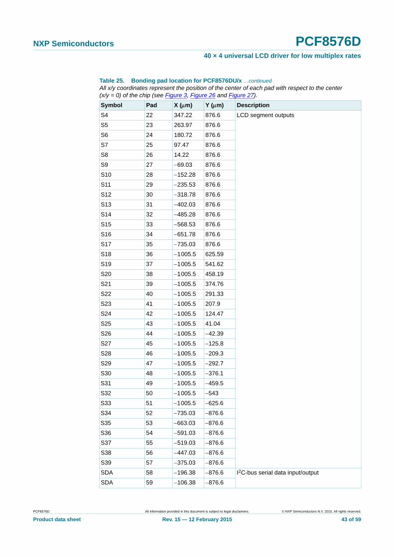
S4 22 347.22 876.6 LCD segment outputs
S5 23 263.97 876.6
S6 24 180.72 876.6
S7 25 97.47 876.6
S8 26 14.22 876.6
S9 27 69.03 876.6
S10 28 152.28 876.6
S11 29 235.53 876.6
S12 30 318.78 876.6
S13 31 402.03 876.6
S14 32 485.28 876.6
S15 33 568.53 876.6
S16 34 651.78 876.6
S17 35 735.03 876.6
S18 36 1005.5 625.59
S19 37 1005.5 541.62
S20 38 1005.5 458.19
S21 39 1005.5 374.76
S22 40 1005.5 291.33
S23 41 1005.5 207.9
S24 42 1005.5 124.47
S25 43 1005.5 41.04
S26 44 1005.5 42.39
S27 45 1005.5 125.8
S28 46 1005.5 209.3
S29 47 1005.5 292.7
S30 48 1005.5 376.1
S31 49 1005.5 459.5
S32 50 1005.5 543
S33 51 1005.5 625.6
S34 52 735.03 876.6
S35 53 663.03 876.6
S36 54 591.03 876.6
S37 55 519.03 876.6
S38 56 447.03 876.6
S39 57 375.03 876.6
SDA 58 196.38 876.6 I2C-bus serial data input/output
SDA 59 106.38 876.6
Table 25. Bonding pad location for PCF8576DU/x …continuedAll x/y coordinates represent the position of the center of each pad with respect to the center (x/y = 0) of the chip (see Figure 3, Figure 26 and Figure 27).
Symbol Pad X (m) Y (m) Description
PCF8576D All information provided in this document is subject to legal disclaimers. © NXP Semiconductors N.V. 2015. All rights reserved.
Product data sheet Rev. 15 — 12 February 2015 43 of 59
NXP Semiconductors PCF8576D40 × 4 universal LCD driver for low multiplex rates
18. Handling information
All input and output pins are protected against ElectroStatic Discharge (ESD) under normal handling. When handling Metal-Oxide Semiconductor (MOS) devices ensure that all normal precautions are taken as described in JESD625-A, IEC 61340-5 or equivalent standards.
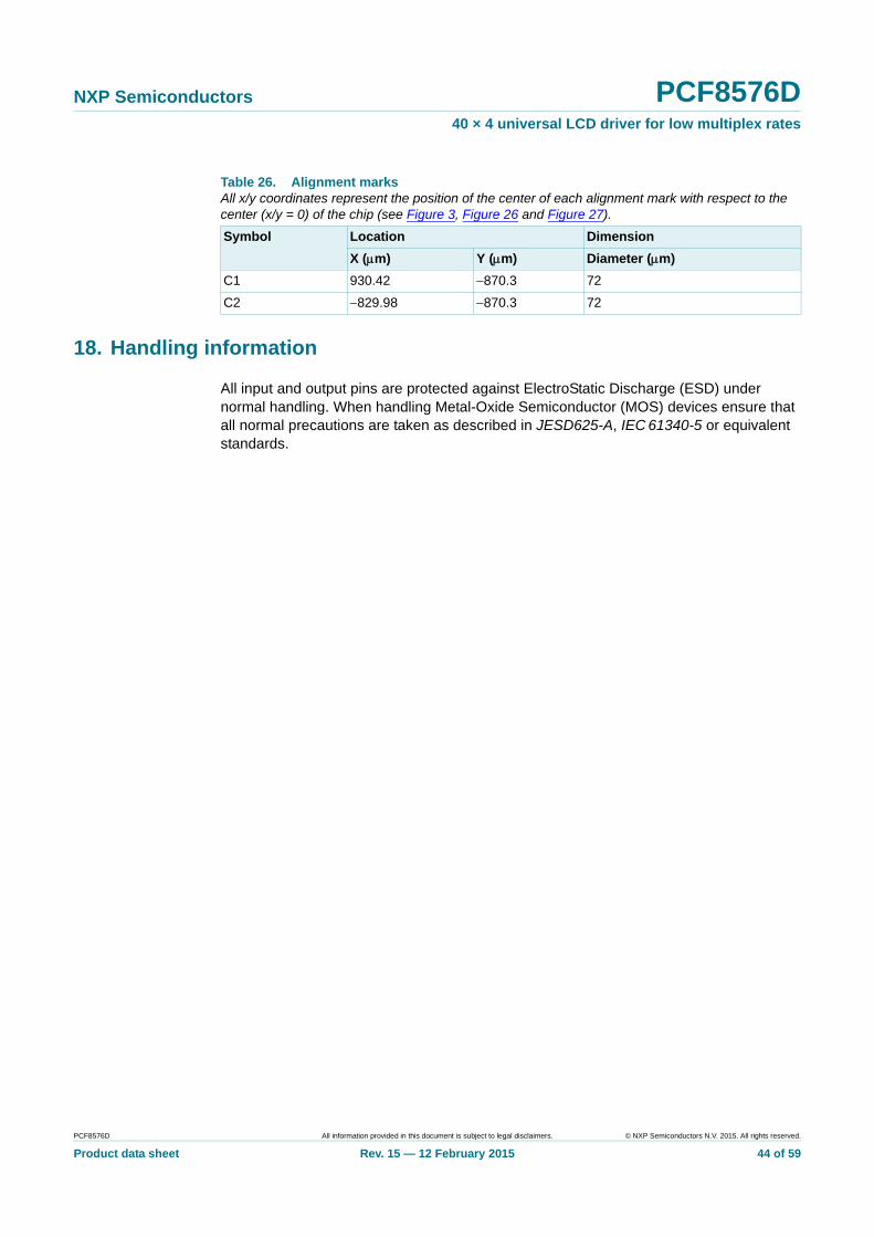
Table 26. Alignment marksAll x/y coordinates represent the position of the center of each alignment mark with respect to the center (x/y = 0) of the chip (see Figure 3, Figure 26 and Figure 27).
Symbol Location Dimension
X (m) Y (m) Diameter (m)
C1 930.42 870.3 72
C2 829.98 870.3 72
PCF8576D All information provided in this document is subject to legal disclaimers. © NXP Semiconductors N.V. 2015. All rights reserved.
Product data sheet Rev. 15 — 12 February 2015 44 of 59
NXP Semiconductors PCF8576D40 × 4 universal LCD driver for low multiplex rates
19. Packing information
19.1 Tray information
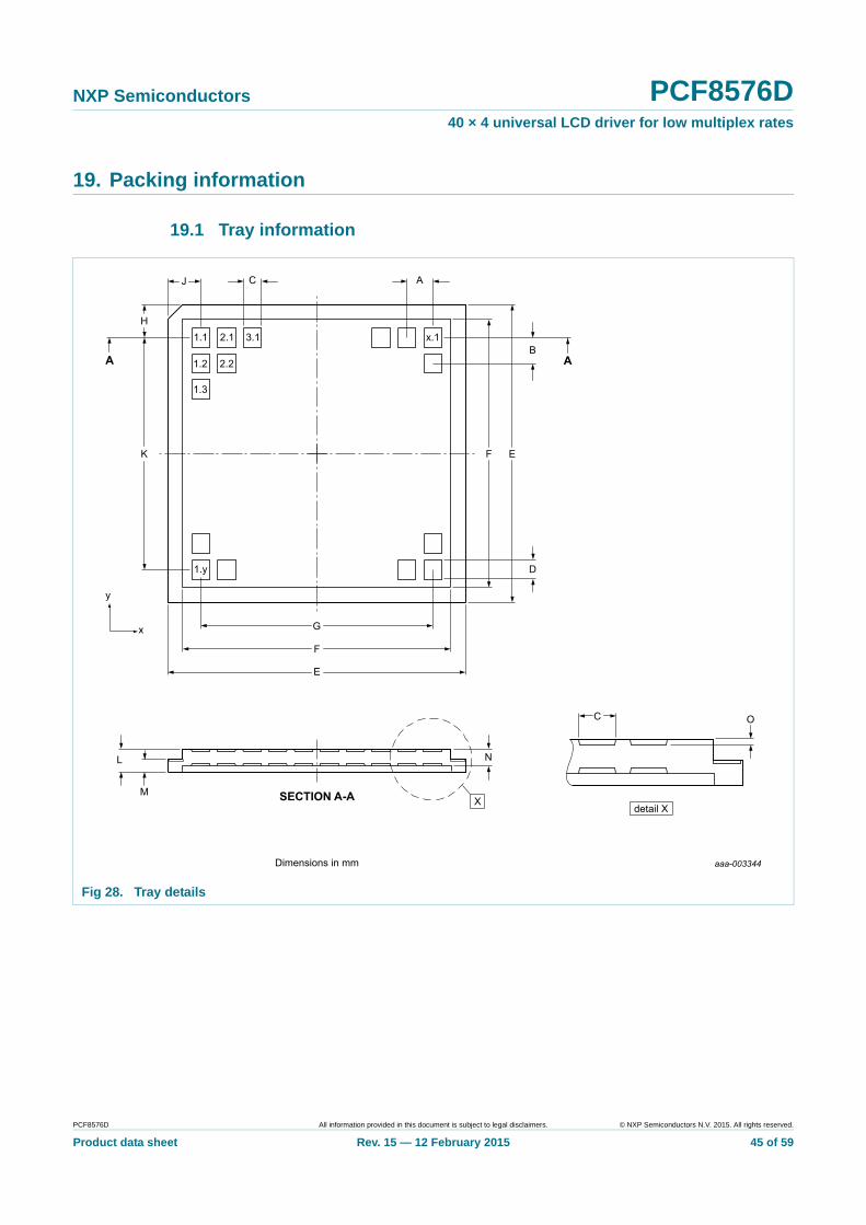
Fig 28. Tray details
PCF8576D All information provided in this document is subject to legal disclaimers. © NXP Semiconductors N.V. 2015. All rights reserved.
Product data sheet Rev. 15 — 12 February 2015 45 of 59
NXP Semiconductors PCF8576D40 × 4 universal LCD driver for low multiplex rates
19.2 Tape and reel information
For tape and reel packing information, please see Ref. 13 “SOT364-1_118” on page 53.
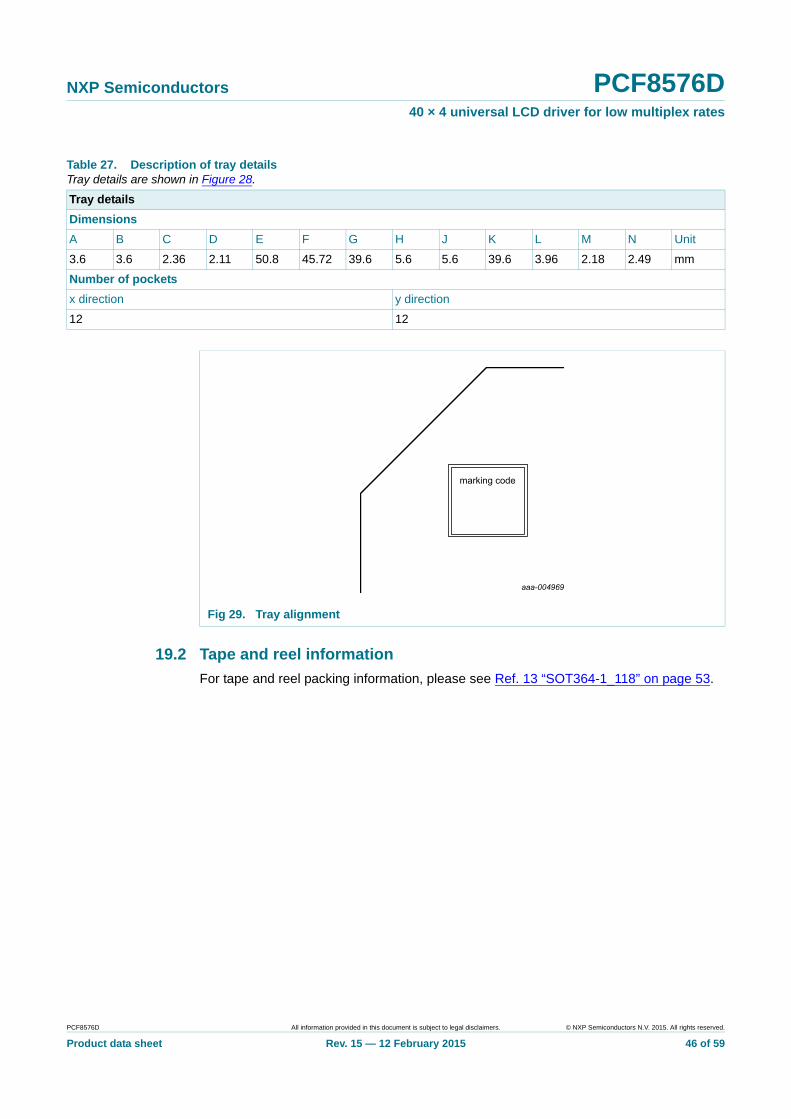
Table 27. Description of tray detailsTray details are shown in Figure 28.
Tray details
Dimensions
A B C D E F G H J K L M N Unit
3.6 3.6 2.36 2.11 50.8 45.72 39.6 5.6 5.6 39.6 3.96 2.18 2.49 mm
Number of pockets
x direction y direction
12 12
Fig 29. Tray alignment
PCF8576D All information provided in this document is subject to legal disclaimers. © NXP Semiconductors N.V. 2015. All rights reserved.
Product data sheet Rev. 15 — 12 February 2015 46 of 59
NXP Semiconductors PCF8576D40 × 4 universal LCD driver for low multiplex rates
20. Soldering of SMD packages
This text provides a very brief insight into a complex technology. A more in-depth account of soldering ICs can be found in Application Note AN10365 “Surface mount reflow soldering description”.
20.1 Introduction to soldering
Soldering is one of the most common methods through which packages are attached to Printed Circuit Boards (PCBs), to form electrical circuits. The soldered joint provides both the mechanical and the electrical connection. There is no single soldering method that is ideal for all IC packages. Wave soldering is often preferred when through-hole and Surface Mount Devices (SMDs) are mixed on one printed wiring board; however, it is not suitable for fine pitch SMDs. Reflow soldering is ideal for the small pitches and high densities that come with increased miniaturization.
20.2 Wave and reflow soldering
Wave soldering is a joining technology in which the joints are made by solder coming from a standing wave of liquid solder. The wave soldering process is suitable for the following:
• Through-hole components
• Leaded or leadless SMDs, which are glued to the surface of the printed circuit board
Not all SMDs can be wave soldered. Packages with solder balls, and some leadless packages which have solder lands underneath the body, cannot be wave soldered. Also, leaded SMDs with leads having a pitch smaller than ~0.6 mm cannot be wave soldered, due to an increased probability of bridging.
The reflow soldering process involves applying solder paste to a board, followed by component placement and exposure to a temperature profile. Leaded packages, packages with solder balls, and leadless packages are all reflow solderable.
Key characteristics in both wave and reflow soldering are:
• Board specifications, including the board finish, solder masks and vias
• Package footprints, including solder thieves and orientation
• The moisture sensitivity level of the packages
• Package placement
• Inspection and repair
• Lead-free soldering versus SnPb soldering
20.3 Wave soldering
Key characteristics in wave soldering are:
• Process issues, such as application of adhesive and flux, clinching of leads, board transport, the solder wave parameters, and the time during which components are exposed to the wave
• Solder bath specifications, including temperature and impurities
PCF8576D All information provided in this document is subject to legal disclaimers. © NXP Semiconductors N.V. 2015. All rights reserved.
Product data sheet Rev. 15 — 12 February 2015 47 of 59
NXP Semiconductors PCF8576D40 × 4 universal LCD driver for low multiplex rates
20.4 Reflow soldering
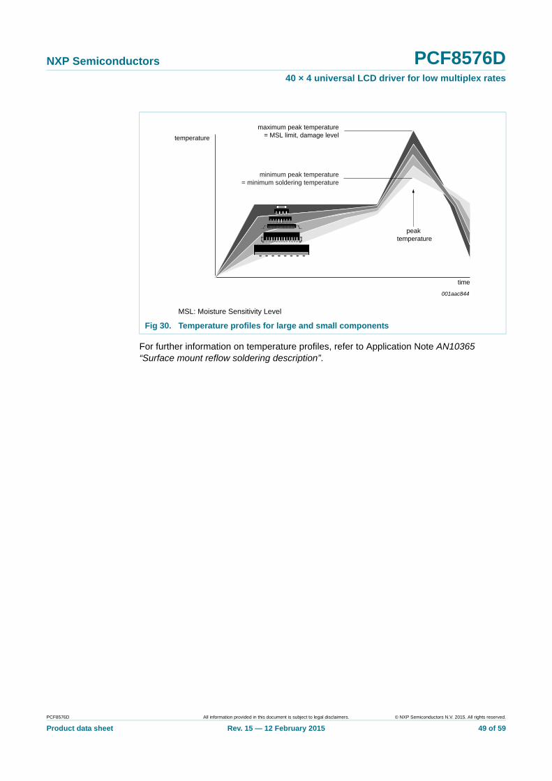
Key characteristics in reflow soldering are:
• Lead-free versus SnPb soldering; note that a lead-free reflow process usually leads to higher minimum peak temperatures (see Figure 30) than a SnPb process, thus reducing the process window
• Solder paste printing issues including smearing, release, and adjusting the process window for a mix of large and small components on one board
• Reflow temperature profile; this profile includes preheat, reflow (in which the board is heated to the peak temperature) and cooling down. It is imperative that the peak temperature is high enough for the solder to make reliable solder joints (a solder paste characteristic). In addition, the peak temperature must be low enough that the packages and/or boards are not damaged. The peak temperature of the package depends on package thickness and volume and is classified in accordance with Table 28 and 29
Moisture sensitivity precautions, as indicated on the packing, must be respected at all times.
Studies have shown that small packages reach higher temperatures during reflow soldering, see Figure 30.
Table 28. SnPb eutectic process (from J-STD-020D)
Package thickness (mm) Package reflow temperature (C)
Volume (mm3)
< 350 350
< 2.5 235 220
2.5 220 220
Table 29. Lead-free process (from J-STD-020D)
Package thickness (mm) Package reflow temperature (C)
Volume (mm3)
< 350 350 to 2000 > 2000
< 1.6 260 260 260
1.6 to 2.5 260 250 245
> 2.5 250 245 245
PCF8576D All information provided in this document is subject to legal disclaimers. © NXP Semiconductors N.V. 2015. All rights reserved.
Product data sheet Rev. 15 — 12 February 2015 48 of 59
NXP Semiconductors PCF8576D40 × 4 universal LCD driver for low multiplex rates
For further information on temperature profiles, refer to Application Note AN10365 “Surface mount reflow soldering description”.
MSL: Moisture Sensitivity Level
Fig 30. Temperature profiles for large and small components
001aac844
temperature
time
minimum peak temperature= minimum soldering temperature
maximum peak temperature= MSL limit, damage level
peak temperature
PCF8576D All information provided in this document is subject to legal disclaimers. © NXP Semiconductors N.V. 2015. All rights reserved.
Product data sheet Rev. 15 — 12 February 2015 49 of 59
xxxxxxxxxxxxxxxxxxxxx xxxxxxxxxxxxxxxxxxxxxxxxxx xxxxxxx x x x xxxxxxxxxxxxxxxxxxxxxxxxxxxxxx xxxxxxxxxxxxxxxxxxx xx xx xxxxx xxxxxxxxxxxxxxxxxxxxxxxxxxx xxxxxxxxxxxxxxxxxxx xxxxxx xxxxxxxxxxxxxxxxxxxxxxxxxxxxxxxxxxx xxxxxxxxxxxx x x xxxxxxxxxxxxxxxxxxxxx xxxxxxxxxxxxxxxxxxxxxxxxxxxxxx xxxxx xxxxxxxxxxxxxxxxxxxxxxxxxxxxxxxxxxxxxxxxxxxxxxxxxx xxxxxxxx xxxxxxxxxxxxxxxxxxxxxxxxx xxxxxxxxxxxxxxxxxxxx xxx
PC
F85
76D
Pro
du
ct data sh
NX
P S
emico
nd
ucto
rsP
CF
8576D4
0 ×
4 u
niv
ers
al L
CD
drive
r for lo
w m
ultip
lex
rates
21. Appendix
21.1 LCD segment driver selection
amb (C) Interface Package AEC-Q100
40 to 105 I2C / SPI TSSOP56 Y
40 to 95 I2C TSSOP56 Y
40 to 95 SPI TSSOP56 Y
40 to 95 I2C TQFP64 Y
40 to 95 SPI TQFP64 Y
40 to 85 I2C LQFP80 N
40 to 95 I2C LQFP80 Y
40 to 105 I2C LQFP80 Y
40 to 85 I2C TSSOP56 N
40 to 85 SPI TSSOP56 N
40 to 85 I2C TSSOP56 N
40 to 85 SPI TSSOP56 N
40 to 95 I2C TSSOP56 Y
40 to 95 SPI TSSOP56 Y
40 to 85 I2C TQFP64 N
40 to 85 SPI TQFP64 N
40 to 95 I2C TQFP64 Y
40 to 95 SPI TQFP64 Y
40 to 105 I2C LQFP80 Y
40 to 105 I2C Bare die Y
40 to 85 I2C Bare die N
40 to 85 I2C Bare die N
40 to 105 I2C Bare die Y
40 to 85 I2C Bare die N
40 to 95 I2C Bare die Y
All inform
ation provided
in this docum
ent is subject to leg
al disclaim
ers.©
NX
P S
em
iconductors N
.V. 2015. A
ll rights re
served.
eetR
ev. 15 — 12 F
ebru
ary 2015
50 of 59
Table 30. Selection of LCD segment drivers
Type name Number of elements at MUX VDD (V) VLCD (V) ffr (Hz) VLCD (V) charge pump
VLCD (V) temperature compensat.
T
1:1 1:2 1:3 1:4 1:6 1:8 1:9
PCA8553DTT 40 80 120 160 - - - 1.8 to 5.5 1.8 to 5.5 32 to 256[1] N N
PCA8546ATT - - - 176 - - - 1.8 to 5.5 2.5 to 9 60 to 300[1] N N
PCA8546BTT - - - 176 - - - 1.8 to 5.5 2.5 to 9 60 to 300[1] N N
PCA8547AHT 44 88 - 176 - - - 1.8 to 5.5 2.5 to 9 60 to 300[1] Y Y
PCA8547BHT 44 88 - 176 - - - 1.8 to 5.5 2.5 to 9 60 to 300[1] Y Y
PCF85134HL 60 120 180 240 - - - 1.8 to 5.5 2.5 to 6.5 82 N N
PCA85134H 60 120 180 240 - - - 1.8 to 5.5 2.5 to 8 82 N N
PCA8543AHL 60 120 - 240 - - - 2.5 to 5.5 2.5 to 9 60 to 300[1] Y Y
PCF8545ATT - - - 176 252 320 - 1.8 to 5.5 2.5 to 5.5 60 to 300[1] N N
PCF8545BTT - - - 176 252 320 - 1.8 to 5.5 2.5 to 5.5 60 to 300[1] N N
PCF8536AT - - - 176 252 320 - 1.8 to 5.5 2.5 to 9 60 to 300[1] N N
PCF8536BT - - - 176 252 320 - 1.8 to 5.5 2.5 to 9 60 to 300[1] N N
PCA8536AT - - - 176 252 320 - 1.8 to 5.5 2.5 to 9 60 to 300[1] N N
PCA8536BT - - - 176 252 320 - 1.8 to 5.5 2.5 to 9 60 to 300[1] N N
PCF8537AH 44 88 - 176 276 352 - 1.8 to 5.5 2.5 to 9 60 to 300[1] Y Y
PCF8537BH 44 88 - 176 276 352 - 1.8 to 5.5 2.5 to 9 60 to 300[1] Y Y
PCA8537AH 44 88 - 176 276 352 - 1.8 to 5.5 2.5 to 9 60 to 300[1] Y Y
PCA8537BH 44 88 - 176 276 352 - 1.8 to 5.5 2.5 to 9 60 to 300[1] Y Y
PCA9620H 60 120 - 240 320 480 - 2.5 to 5.5 2.5 to 9 60 to 300[1] Y Y
PCA9620U 60 120 - 240 320 480 - 2.5 to 5.5 2.5 to 9 60 to 300[1] Y Y
PCF8576DU 40 80 120 160 - - - 1.8 to 5.5 2.5 to 6.5 77 N N
PCF8576EUG 40 80 120 160 - - - 1.8 to 5.5 2.5 to 6.5 77 N N
PCA8576FUG 40 80 120 160 - - - 1.8 to 5.5 2.5 to 8 200 N N
PCF85133U 80 160 240 320 - - - 1.8 to 5.5 2.5 to 6.5 82, 110[2] N N
PCA85133U 80 160 240 320 - - - 1.8 to 5.5 2.5 to 8 82, 110[2] N N
xxxxxxxxxxxxxxxxxxxxx xxxxxxxxxxxxxxxxxxxxxxxxxx xxxxxxx x x x xxxxxxxxxxxxxxxxxxxxxxxxxxxxxx xxxxxxxxxxxxxxxxxxx xx xx xxxxx xxxxxxxxxxxxxxxxxxxxxxxxxxx xxxxxxxxxxxxxxxxxxx xxxxxx xxxxxxxxxxxxxxxxxxxxxxxxxxxxxxxxxxx xxxxxxxxxxxx x x xxxxxxxxxxxxxxxxxxxxx xxxxxxxxxxxxxxxxxxxxxxxxxxxxxx xxxxx xxxxxxxxxxxxxxxxxxxxxxxxxxxxxxxxxxxxxxxxxxxxxxxxxx xxxxxxxx xxxxxxxxxxxxxxxxxxxxxxxxx xxxxxxxxxxxxxxxxxxxx xxx
PC
F85
76D
Pro
du
ct data sh
NX
P S
emico
nd
ucto
rsP
CF
8576D4
0 ×
4 u
niv
ers
al L
CD
drive
r for lo
w m
ultip
lex
rates
PCA85233UG 80 160 240 320 - - - 1.8 to 5.5 2.5 to 8 150, 220[2] N N 40 to 105 I2C Bare die Y
40 to 85 I2C Bare die N
40 to 105 I2C / SPI Bare die Y
40 to 95 I2C Bare die Y
40 to 95 I2C Bare die Y
40 to 85 I2C / SPI Bare die N
40 to 105 I2C / SPI Bare die Y
Table 30. Selection of LCD segment drivers …continued
Type name Number of elements at MUX VDD (V) VLCD (V) ffr (Hz) VLCD (V) charge pump
VLCD (V) temperature compensat.
Tamb (C) Interface Package AEC-Q1001:1 1:2 1:3 1:4 1:6 1:8 1:9
All inform
ation provided
in this docum
ent is subject to leg
al disclaim
ers.©
NX
P S
em
iconductors N
.V. 2015. A
ll rights re
served.
eetR
ev. 15 — 12 F
ebru
ary 2015
51 of 59
[1] Software programmable.
[2] Hardware selectable.
PCF85132U 160 320 480 640 - - - 1.8 to 5.5 1.8 to 8 60 to 90[1] N N
PCA8530DUG 102 204 - 408 - - - 2.5 to 5.5 4 to 12 45 to 300[1] Y Y
PCA85132U 160 320 480 640 - - - 1.8 to 5.5 1.8 to 8 60 to 90[1] N N
PCA85232U 160 320 480 640 - - - 1.8 to 5.5 1.8 to 8 117 to 176[1] N N
PCF8538UG 102 204 - 408 612 816 918 2.5 to 5.5 4 to 12 45 to 300[1] Y Y
PCA8538UG 102 204 - 408 612 816 918 2.5 to 5.5 4 to 12 45 to 300[1] Y Y
NXP Semiconductors PCF8576D40 × 4 universal LCD driver for low multiplex rates
22. Abbreviations
Table 31. Abbreviations
Acronym Description
CDM Charged-Device Model
CMOS Complementary Metal-Oxide Semiconductor
HBM Human Body Model
ITO Indium Tin Oxide
LCD Liquid Crystal Display
LSB Least Significant Bit
MM Machine Model
MSB Most Significant Bit
MSL Moisture Sensitivity Level
PCB Printed Circuit Board
RAM Random Access Memory
RMS Root Mean Square
SCL Serial CLock line
SDA Serial DAta line
SMD Surface Mount Device
PCF8576D All information provided in this document is subject to legal disclaimers. © NXP Semiconductors N.V. 2015. All rights reserved.
Product data sheet Rev. 15 — 12 February 2015 52 of 59
NXP Semiconductors PCF8576D40 × 4 universal LCD driver for low multiplex rates
23. References
[1] AN10170 — Design guidelines for COG modules with NXP monochrome LCD drivers
[2] AN10365 — Surface mount reflow soldering description
[3] AN10706 — Handling bare die
[4] AN10853 — ESD and EMC sensitivity of IC
[5] IEC 60134 — Rating systems for electronic tubes and valves and analogous semiconductor devices
[6] IEC 61340-5 — Protection of electronic devices from electrostatic phenomena
[7] IPC/JEDEC J-STD-020D — Moisture/Reflow Sensitivity Classification for Nonhermetic Solid State Surface Mount Devices
[8] JESD22-A114 — Electrostatic Discharge (ESD) Sensitivity Testing Human Body Model (HBM)
[9] JESD22-A115 — Electrostatic Discharge (ESD) Sensitivity Testing Machine Model (MM)
[10] JESD22-C101 — Field-Induced Charged-Device Model Test Method for Electrostatic-Discharge-Withstand Thresholds of Microelectronic Components
[11] JESD78 — IC Latch-Up Test
[12] JESD625-A — Requirements for Handling Electrostatic-Discharge-Sensitive (ESDS) Devices
[13] SOT364-1_118 — TSSOP56; Reel pack; SMD, 13", packing information
[14] UM10204 — I2C-bus specification and user manual
[15] UM10569 — Store and transport requirements
PCF8576D All information provided in this document is subject to legal disclaimers. © NXP Semiconductors N.V. 2015. All rights reserved.
Product data sheet Rev. 15 — 12 February 2015 53 of 59
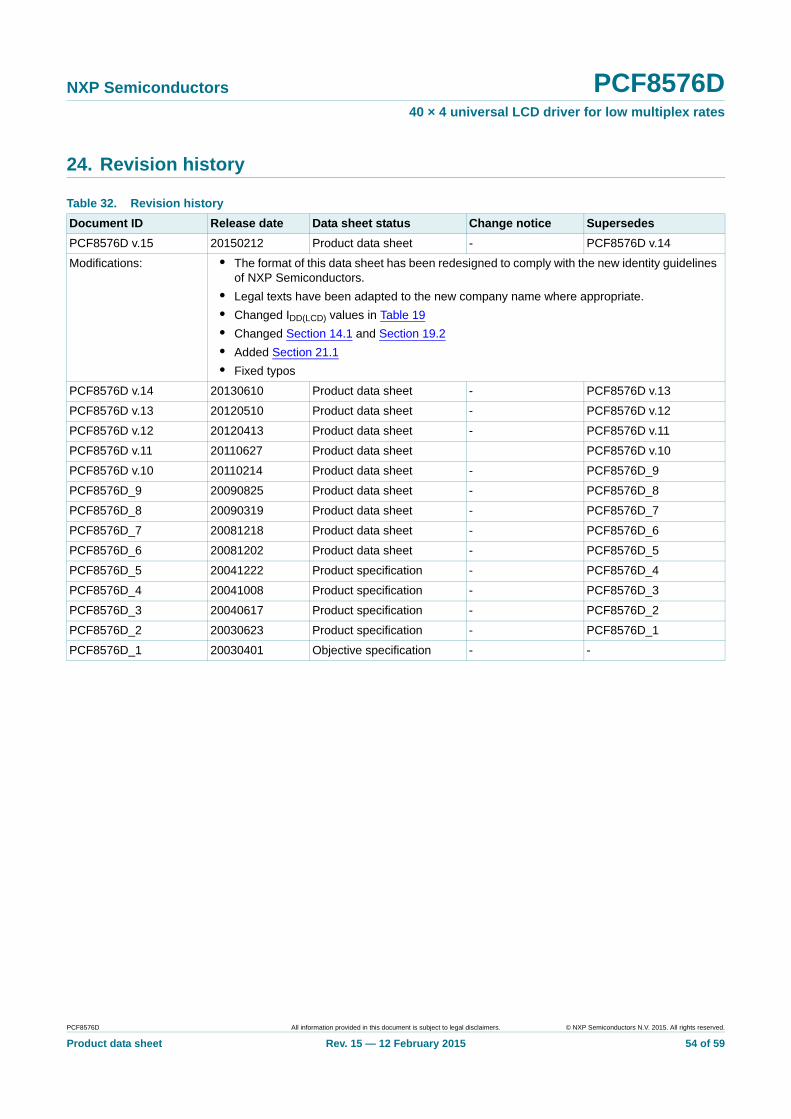
NXP Semiconductors PCF8576D40 × 4 universal LCD driver for low multiplex rates
24. Revision history
Table 32. Revision history
Document ID Release date Data sheet status Change notice Supersedes
PCF8576D v.15 20150212 Product data sheet - PCF8576D v.14
Modifications: • The format of this data sheet has been redesigned to comply with the new identity guidelines of NXP Semiconductors.
• Legal texts have been adapted to the new company name where appropriate.
• Changed IDD(LCD) values in Table 19
• Changed Section 14.1 and Section 19.2
• Added Section 21.1
• Fixed typos
PCF8576D v.14 20130610 Product data sheet - PCF8576D v.13
PCF8576D v.13 20120510 Product data sheet - PCF8576D v.12
PCF8576D v.12 20120413 Product data sheet - PCF8576D v.11
PCF8576D v.11 20110627 Product data sheet PCF8576D v.10
PCF8576D v.10 20110214 Product data sheet - PCF8576D_9
PCF8576D_9 20090825 Product data sheet - PCF8576D_8
PCF8576D_8 20090319 Product data sheet - PCF8576D_7
PCF8576D_7 20081218 Product data sheet - PCF8576D_6
PCF8576D_6 20081202 Product data sheet - PCF8576D_5
PCF8576D_5 20041222 Product specification - PCF8576D_4
PCF8576D_4 20041008 Product specification - PCF8576D_3
PCF8576D_3 20040617 Product specification - PCF8576D_2
PCF8576D_2 20030623 Product specification - PCF8576D_1
PCF8576D_1 20030401 Objective specification - -
PCF8576D All information provided in this document is subject to legal disclaimers. © NXP Semiconductors N.V. 2015. All rights reserved.
Product data sheet Rev. 15 — 12 February 2015 54 of 59
NXP Semiconductors PCF8576D40 × 4 universal LCD driver for low multiplex rates
25. Legal information
25.1 Data sheet status
[1] Please consult the most recently issued document before initiating or completing a design.
[2] The term ‘short data sheet’ is explained in section “Definitions”.
[3] The product status of device(s) described in this document may have changed since this document was published and may differ in case of multiple devices. The latest product status information is available on the Internet at URL http://www.nxp.com.
25.2 Definitions
Draft — The document is a draft version only. The content is still under internal review and subject to formal approval, which may result in modifications or additions. NXP Semiconductors does not give any representations or warranties as to the accuracy or completeness of information included herein and shall have no liability for the consequences of use of such information.
Short data sheet — A short data sheet is an extract from a full data sheet with the same product type number(s) and title. A short data sheet is intended for quick reference only and should not be relied upon to contain detailed and full information. For detailed and full information see the relevant full data sheet, which is available on request via the local NXP Semiconductors sales office. In case of any inconsistency or conflict with the short data sheet, the full data sheet shall prevail.
Product specification — The information and data provided in a Product data sheet shall define the specification of the product as agreed between NXP Semiconductors and its customer, unless NXP Semiconductors and customer have explicitly agreed otherwise in writing. In no event however, shall an agreement be valid in which the NXP Semiconductors product is deemed to offer functions and qualities beyond those described in the Product data sheet.
25.3 Disclaimers
Limited warranty and liability — Information in this document is believed to be accurate and reliable. However, NXP Semiconductors does not give any representations or warranties, expressed or implied, as to the accuracy or completeness of such information and shall have no liability for the consequences of use of such information. NXP Semiconductors takes no responsibility for the content in this document if provided by an information source outside of NXP Semiconductors.
In no event shall NXP Semiconductors be liable for any indirect, incidental, punitive, special or consequential damages (including - without limitation - lost profits, lost savings, business interruption, costs related to the removal or replacement of any products or rework charges) whether or not such damages are based on tort (including negligence), warranty, breach of contract or any other legal theory.
Notwithstanding any damages that customer might incur for any reason whatsoever, NXP Semiconductors’ aggregate and cumulative liability towards customer for the products described herein shall be limited in accordance with the Terms and conditions of commercial sale of NXP Semiconductors.
Right to make changes — NXP Semiconductors reserves the right to make changes to information published in this document, including without limitation specifications and product descriptions, at any time and without notice. This document supersedes and replaces all information supplied prior to the publication hereof.
Suitability for use — NXP Semiconductors products are not designed, authorized or warranted to be suitable for use in life support, life-critical or safety-critical systems or equipment, nor in applications where failure or malfunction of an NXP Semiconductors product can reasonably be expected to result in personal injury, death or severe property or environmental damage. NXP Semiconductors and its suppliers accept no liability for inclusion and/or use of NXP Semiconductors products in such equipment or applications and therefore such inclusion and/or use is at the customer’s own risk.
Applications — Applications that are described herein for any of these products are for illustrative purposes only. NXP Semiconductors makes no representation or warranty that such applications will be suitable for the specified use without further testing or modification.
Customers are responsible for the design and operation of their applications and products using NXP Semiconductors products, and NXP Semiconductors accepts no liability for any assistance with applications or customer product design. It is customer’s sole responsibility to determine whether the NXP Semiconductors product is suitable and fit for the customer’s applications and products planned, as well as for the planned application and use of customer’s third party customer(s). Customers should provide appropriate design and operating safeguards to minimize the risks associated with their applications and products.
NXP Semiconductors does not accept any liability related to any default, damage, costs or problem which is based on any weakness or default in the customer’s applications or products, or the application or use by customer’s third party customer(s). Customer is responsible for doing all necessary testing for the customer’s applications and products using NXP Semiconductors products in order to avoid a default of the applications and the products or of the application or use by customer’s third party customer(s). NXP does not accept any liability in this respect.
Limiting values — Stress above one or more limiting values (as defined in the Absolute Maximum Ratings System of IEC 60134) will cause permanent damage to the device. Limiting values are stress ratings only and (proper) operation of the device at these or any other conditions above those given in the Recommended operating conditions section (if present) or the Characteristics sections of this document is not warranted. Constant or repeated exposure to limiting values will permanently and irreversibly affect the quality and reliability of the device.
Terms and conditions of commercial sale — NXP Semiconductors products are sold subject to the general terms and conditions of commercial sale, as published at http://www.nxp.com/profile/terms, unless otherwise agreed in a valid written individual agreement. In case an individual agreement is concluded only the terms and conditions of the respective agreement shall apply. NXP Semiconductors hereby expressly objects to applying the customer’s general terms and conditions with regard to the purchase of NXP Semiconductors products by customer.
No offer to sell or license — Nothing in this document may be interpreted or construed as an offer to sell products that is open for acceptance or the grant, conveyance or implication of any license under any copyrights, patents or other industrial or intellectual property rights.
Document status[1][2] Product status[3] Definition
Objective [short] data sheet Development This document contains data from the objective specification for product development.
Preliminary [short] data sheet Qualification This document contains data from the preliminary specification.
Product [short] data sheet Production This document contains the product specification.
PCF8576D All information provided in this document is subject to legal disclaimers. © NXP Semiconductors N.V. 2015. All rights reserved.
Product data sheet Rev. 15 — 12 February 2015 55 of 59
NXP Semiconductors PCF8576D40 × 4 universal LCD driver for low multiplex rates
Export control — This document as well as the item(s) described herein may be subject to export control regulations. Export might require a prior authorization from competent authorities.
Non-automotive qualified products — Unless this data sheet expressly states that this specific NXP Semiconductors product is automotive qualified, the product is not suitable for automotive use. It is neither qualified nor tested in accordance with automotive testing or application requirements. NXP Semiconductors accepts no liability for inclusion and/or use of non-automotive qualified products in automotive equipment or applications.
In the event that customer uses the product for design-in and use in automotive applications to automotive specifications and standards, customer (a) shall use the product without NXP Semiconductors’ warranty of the product for such automotive applications, use and specifications, and (b) whenever customer uses the product for automotive applications beyond NXP Semiconductors’ specifications such use shall be solely at customer’s own risk, and (c) customer fully indemnifies NXP Semiconductors for any liability, damages or failed product claims resulting from customer design and use of the product for automotive applications beyond NXP Semiconductors’ standard warranty and NXP Semiconductors’ product specifications.
Translations — A non-English (translated) version of a document is for reference only. The English version shall prevail in case of any discrepancy between the translated and English versions.
Bare die — All die are tested on compliance with their related technical specifications as stated in this data sheet up to the point of wafer sawing and are handled in accordance with the NXP Semiconductors storage and transportation conditions. If there are data sheet limits not guaranteed, these will be separately indicated in the data sheet. There are no post-packing tests performed on individual die or wafers.
NXP Semiconductors has no control of third party procedures in the sawing, handling, packing or assembly of the die. Accordingly, NXP Semiconductors assumes no liability for device functionality or performance of the die or systems after third party sawing, handling, packing or assembly of the die. It is the responsibility of the customer to test and qualify their application in which the die is used.
All die sales are conditioned upon and subject to the customer entering into a written die sale agreement with NXP Semiconductors through its legal department.
25.4 TrademarksNotice: All referenced brands, product names, service names and trademarks are the property of their respective owners.
I2C-bus — logo is a trademark of NXP Semiconductors N.V.
26. Contact information
For more information, please visit: http://www.nxp.com
For sales office addresses, please send an email to: [email protected]
PCF8576D All information provided in this document is subject to legal disclaimers. © NXP Semiconductors N.V. 2015. All rights reserved.
Product data sheet Rev. 15 — 12 February 2015 56 of 59
NXP Semiconductors PCF8576D40 × 4 universal LCD driver for low multiplex rates
27. Tables
Table 1. Ordering information . . . . . . . . . . . . . . . . . . . . .2Table 2. Ordering options . . . . . . . . . . . . . . . . . . . . . . . . .2Table 3. Marking codes . . . . . . . . . . . . . . . . . . . . . . . . . .2Table 4. Pin description . . . . . . . . . . . . . . . . . . . . . . . . . .6Table 5. Selection of possible display configurations . . . .7Table 6. Biasing characteristics . . . . . . . . . . . . . . . . . . . .9Table 7. Standard RAM filling in 1:3 multiplex drive
mode. . . . . . . . . . . . . . . . . . . . . . . . . . . . . . . . .21Table 8. Entire RAM filling by rewriting in 1:3 multiplex
drive mode . . . . . . . . . . . . . . . . . . . . . . . . . . . .21Table 9. Blinking frequencies . . . . . . . . . . . . . . . . . . . . .23Table 10. Definition of PCF8576D commands . . . . . . . .23Table 11. C bit description . . . . . . . . . . . . . . . . . . . . . . . .23Table 12. Mode-set command bit description . . . . . . . . .24Table 13. Load-data-pointer command bit description . . .24Table 14. Device-select command bit description . . . . . .24Table 15. Bank-select command bit description . . . . . . .25Table 16. Blink-select command bit description . . . . . . . .25Table 17. I2C slave address byte . . . . . . . . . . . . . . . . . . .28Table 18. Limiting values . . . . . . . . . . . . . . . . . . . . . . . . .32Table 19. Static characteristics . . . . . . . . . . . . . . . . . . . .33Table 20. Dynamic characteristics . . . . . . . . . . . . . . . . . .34Table 21. Addressing cascaded PCF8576D . . . . . . . . . .36Table 22. SYNC contact resistance . . . . . . . . . . . . . . . . .37Table 23. Dimensions of PCF8576DU/DA . . . . . . . . . . . .42Table 24. Dimensions of PCF8576DU/2DA . . . . . . . . . . .42Table 25. Bonding pad location for PCF8576DU/x . . . . .42Table 26. Alignment marks. . . . . . . . . . . . . . . . . . . . . . . .44Table 27. Description of tray details . . . . . . . . . . . . . . . . .46Table 28. SnPb eutectic process (from J-STD-020D) . . .48Table 29. Lead-free process (from J-STD-020D) . . . . . .48Table 30. Selection of LCD segment drivers . . . . . . . . . .50Table 31. Abbreviations . . . . . . . . . . . . . . . . . . . . . . . . . .52Table 32. Revision history . . . . . . . . . . . . . . . . . . . . . . . .54
PCF8576D All information provided in this document is subject to legal disclaimers. © NXP Semiconductors N.V. 2015. All rights reserved.
Product data sheet Rev. 15 — 12 February 2015 57 of 59
NXP Semiconductors PCF8576D40 × 4 universal LCD driver for low multiplex rates
28. Figures
Fig 1. Block diagram of PCF8576D . . . . . . . . . . . . . . . . .3Fig 2. Pinning diagram for PCF8576DT (TSSOP56) . . . .4Fig 3. Pinning diagram for PCF8576DU (bare die) . . . . .5Fig 4. Example of displays suitable for PCF8576D . . . . .7Fig 5. Typical system configuration . . . . . . . . . . . . . . . . .8Fig 6. Electro-optical characteristic: relative
transmission curve of the liquid . . . . . . . . . . . . . . 11Fig 7. Static drive mode waveforms. . . . . . . . . . . . . . . .12Fig 8. Waveforms for the 1:2 multiplex drive mode
with 1⁄2 bias . . . . . . . . . . . . . . . . . . . . . . . . . . . . .13Fig 9. Waveforms for the 1:2 multiplex drive mode
with 1⁄3 bias . . . . . . . . . . . . . . . . . . . . . . . . . . . . .14Fig 10. Waveforms for the 1:3 multiplex drive mode
with 1⁄3 bias . . . . . . . . . . . . . . . . . . . . . . . . . . . . .15Fig 11. Waveforms for the 1:4 multiplex drive mode
with 1⁄3 bias . . . . . . . . . . . . . . . . . . . . . . . . . . . . .16Fig 12. Display RAM bit map . . . . . . . . . . . . . . . . . . . . . .18Fig 13. Relationship between LCD layout, drive mode,
display RAM filling order and display data transmitted over the I2C-bus . . . . . . . . . . . . . . . .19
Fig 14. Bit transfer . . . . . . . . . . . . . . . . . . . . . . . . . . . . . .26Fig 15. Definition of START and STOP conditions. . . . . .26Fig 16. System configuration . . . . . . . . . . . . . . . . . . . . . .27Fig 17. Acknowledgement of the I2C-bus . . . . . . . . . . . .27Fig 18. I2C-bus protocol . . . . . . . . . . . . . . . . . . . . . . . . . .29Fig 19. Format of command byte. . . . . . . . . . . . . . . . . . .29Fig 20. Device protection circuits . . . . . . . . . . . . . . . . . . .30Fig 21. Driver timing waveforms . . . . . . . . . . . . . . . . . . .35Fig 22. I2C-bus timing waveforms . . . . . . . . . . . . . . . . . .35Fig 23. Cascaded PCF8576D configuration . . . . . . . . . .37Fig 24. Synchronization of the cascade for the various
PCF8576D drive modes . . . . . . . . . . . . . . . . . . .38Fig 25. Package outline SOT364-1 (TSSOP56) of
PCF8576DT. . . . . . . . . . . . . . . . . . . . . . . . . . . . .39Fig 26. Bare die outline PCF8576DU/DA (for dimensions
see Table 23) . . . . . . . . . . . . . . . . . . . . . . . . . . . .40Fig 27. Bare die outline PCF8576DU/2DA (for dimensions
see Table 24) . . . . . . . . . . . . . . . . . . . . . . . . . . . .41Fig 28. Tray details . . . . . . . . . . . . . . . . . . . . . . . . . . . . .45Fig 29. Tray alignment . . . . . . . . . . . . . . . . . . . . . . . . . . .46Fig 30. Temperature profiles for large and small
components . . . . . . . . . . . . . . . . . . . . . . . . . . . . .49
PCF8576D All information provided in this document is subject to legal disclaimers. © NXP Semiconductors N.V. 2015. All rights reserved.
Product data sheet Rev. 15 — 12 February 2015 58 of 59
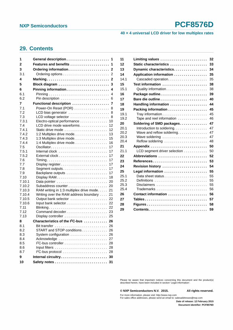
NXP Semiconductors PCF8576D40 × 4 universal LCD driver for low multiplex rates
29. Contents
1 General description . . . . . . . . . . . . . . . . . . . . . . 1
2 Features and benefits . . . . . . . . . . . . . . . . . . . . 1
3 Ordering information. . . . . . . . . . . . . . . . . . . . . 23.1 Ordering options . . . . . . . . . . . . . . . . . . . . . . . . 2
4 Marking . . . . . . . . . . . . . . . . . . . . . . . . . . . . . . . . 2
5 Block diagram . . . . . . . . . . . . . . . . . . . . . . . . . . 3
6 Pinning information. . . . . . . . . . . . . . . . . . . . . . 46.1 Pinning . . . . . . . . . . . . . . . . . . . . . . . . . . . . . . . 46.2 Pin description . . . . . . . . . . . . . . . . . . . . . . . . . 6
7 Functional description . . . . . . . . . . . . . . . . . . . 77.1 Power-On Reset (POR) . . . . . . . . . . . . . . . . . . 87.2 LCD bias generator . . . . . . . . . . . . . . . . . . . . . 87.3 LCD voltage selector . . . . . . . . . . . . . . . . . . . . 87.3.1 Electro-optical performance . . . . . . . . . . . . . . 107.4 LCD drive mode waveforms . . . . . . . . . . . . . . 127.4.1 Static drive mode . . . . . . . . . . . . . . . . . . . . . . 127.4.2 1:2 Multiplex drive mode. . . . . . . . . . . . . . . . . 137.4.3 1:3 Multiplex drive mode. . . . . . . . . . . . . . . . . 157.4.4 1:4 Multiplex drive mode. . . . . . . . . . . . . . . . . 167.5 Oscillator. . . . . . . . . . . . . . . . . . . . . . . . . . . . . 177.5.1 Internal clock . . . . . . . . . . . . . . . . . . . . . . . . . 177.5.2 External clock . . . . . . . . . . . . . . . . . . . . . . . . . 177.6 Timing . . . . . . . . . . . . . . . . . . . . . . . . . . . . . . . 177.7 Display register . . . . . . . . . . . . . . . . . . . . . . . . 177.8 Segment outputs. . . . . . . . . . . . . . . . . . . . . . . 177.9 Backplane outputs . . . . . . . . . . . . . . . . . . . . . 177.10 Display RAM. . . . . . . . . . . . . . . . . . . . . . . . . . 187.10.1 Data pointer . . . . . . . . . . . . . . . . . . . . . . . . . . 207.10.2 Subaddress counter . . . . . . . . . . . . . . . . . . . . 207.10.3 RAM writing in 1:3 multiplex drive mode. . . . . 217.10.4 Writing over the RAM address boundary . . . . 217.10.5 Output bank selector . . . . . . . . . . . . . . . . . . . 227.10.6 Input bank selector . . . . . . . . . . . . . . . . . . . . . 227.11 Blinking . . . . . . . . . . . . . . . . . . . . . . . . . . . . . . 227.12 Command decoder . . . . . . . . . . . . . . . . . . . . . 237.13 Display controller . . . . . . . . . . . . . . . . . . . . . . 25
8 Characteristics of the I2C-bus . . . . . . . . . . . . 268.1 Bit transfer . . . . . . . . . . . . . . . . . . . . . . . . . . . 268.2 START and STOP conditions . . . . . . . . . . . . . 268.3 System configuration . . . . . . . . . . . . . . . . . . . 268.4 Acknowledge . . . . . . . . . . . . . . . . . . . . . . . . . 278.5 I2C-bus controller . . . . . . . . . . . . . . . . . . . . . . 288.6 Input filters . . . . . . . . . . . . . . . . . . . . . . . . . . . 288.7 I2C-bus protocol . . . . . . . . . . . . . . . . . . . . . . . 28
9 Internal circuitry. . . . . . . . . . . . . . . . . . . . . . . . 30
10 Safety notes . . . . . . . . . . . . . . . . . . . . . . . . . . . 31
11 Limiting values . . . . . . . . . . . . . . . . . . . . . . . . 32
12 Static characteristics . . . . . . . . . . . . . . . . . . . 33
13 Dynamic characteristics. . . . . . . . . . . . . . . . . 34
14 Application information . . . . . . . . . . . . . . . . . 3514.1 Cascaded operation. . . . . . . . . . . . . . . . . . . . 35
15 Test information . . . . . . . . . . . . . . . . . . . . . . . 3815.1 Quality information . . . . . . . . . . . . . . . . . . . . . 38
16 Package outline. . . . . . . . . . . . . . . . . . . . . . . . 39
17 Bare die outline . . . . . . . . . . . . . . . . . . . . . . . . 40
18 Handling information . . . . . . . . . . . . . . . . . . . 44
19 Packing information . . . . . . . . . . . . . . . . . . . . 4519.1 Tray information . . . . . . . . . . . . . . . . . . . . . . . 4519.2 Tape and reel information . . . . . . . . . . . . . . . 46
20 Soldering of SMD packages. . . . . . . . . . . . . . 4720.1 Introduction to soldering. . . . . . . . . . . . . . . . . 4720.2 Wave and reflow soldering. . . . . . . . . . . . . . . 4720.3 Wave soldering . . . . . . . . . . . . . . . . . . . . . . . 4720.4 Reflow soldering . . . . . . . . . . . . . . . . . . . . . . 48
21 Appendix . . . . . . . . . . . . . . . . . . . . . . . . . . . . . 5021.1 LCD segment driver selection . . . . . . . . . . . . 50
22 Abbreviations . . . . . . . . . . . . . . . . . . . . . . . . . 52
23 References. . . . . . . . . . . . . . . . . . . . . . . . . . . . 53
24 Revision history . . . . . . . . . . . . . . . . . . . . . . . 54
25 Legal information . . . . . . . . . . . . . . . . . . . . . . 5525.1 Data sheet status . . . . . . . . . . . . . . . . . . . . . . 5525.2 Definitions . . . . . . . . . . . . . . . . . . . . . . . . . . . 5525.3 Disclaimers . . . . . . . . . . . . . . . . . . . . . . . . . . 5525.4 Trademarks . . . . . . . . . . . . . . . . . . . . . . . . . . 56
26 Contact information . . . . . . . . . . . . . . . . . . . . 56
27 Tables . . . . . . . . . . . . . . . . . . . . . . . . . . . . . . . . 57
28 Figures . . . . . . . . . . . . . . . . . . . . . . . . . . . . . . . 58
29 Contents. . . . . . . . . . . . . . . . . . . . . . . . . . . . . . 59
© NXP Semiconductors N.V. 2015. All rights reserved.
For more information, please visit: http://www.nxp.comFor sales office addresses, please send an email to: [email protected]
Date of release: 12 February 2015
Document identifier: PCF8576D
Please be aware that important notices concerning this document and the product(s)described herein, have been included in section ‘Legal information’.