1 FABRICATION PROCESSES FOR NANOMATERIALS
15
Nanostructured Materials - Fabrication Processes 1 FABRICATION PROCESSES FOR NANOMATERIALS 1 Self Assembly SELF-ASSEMBLY • Nanotechnologists want to make macroscopic materials (and structures) by arranging nanoscale building blocks • Could do this using an STM to move each atom (or molecule) into the correct position • A handful of material contains about 10 22 atoms • A very slow process PROCESSING RATE VS. LITHOGRAPHY AND ITS BEST RESOLUTION Photolithography E-beam lithography AFM lithography STM lithography Processing time for 5x5 mm 2 1/10,000 the area single Si wafer - 25 Hours - 3000 Years - 3 billion years - 30 Years - 1/100 sec SELF-ASSEMBLY Need a way to assemble more efficiently • Some useful reference books: • 1. Zhang et al, Self-Assembled Nanostructures • 2. Evans and Wennerstrom, The Colloidal Domain • 3. Ulman, Ultrathin Organic Films 1 2 3 4
Transcript of 1 FABRICATION PROCESSES FOR NANOMATERIALS

Nanostructured Materials - Fabrication Processes 1
FABRICATION PROCESSES FOR NANOMATERIALS
1
Self Assembly
SELF-ASSEMBLY• Nanotechnologists want to make
macroscopic materials (and structures) by arranging nanoscale building blocks
• Could do this using an STM to move each atom (or molecule) into the correct position
• A handful of material contains about 1022 atoms
• A very slow process
PROCESSING RATE VS. LITHOGRAPHY AND ITS BEST
RESOLUTION
PhotolithographyE-beam lithography
AFM lithography
STM lithography
Processing time for 5x5 mm2
1/10,000 the area single Si wafer
-25
Hours
-30
00
Years
-3 billion years
-30
Years
-1/10
0 sec
SELF-ASSEMBLY
Need a way to assemble more efficiently
• Some useful reference books:• 1. Zhang et al, Self-Assembled Nanostructures• 2. Evans and Wennerstrom, The Colloidal Domain• 3. Ulman, Ultrathin Organic Films
1 2
3 4

Nanostructured Materials - Fabrication Processes 2
• Exploit this ability in nanotechnology to make materials from nano-building blocks
• Biomimetics - materials that copy
• natures abilities
SELF-ASSEMBLY -BIOLOGY IS VERY
GOOD AT THIS
Gecko feet
The Cell and Its Hierarchy
ebi.ac.uk
DiatomsWHAT DRIVES SELF ASSEMBLY?
1. Forces between individual particles What forces do we have available?(4)• *covalent, ionic, van der Waals, hydrogen Other forces
• *magnetic, electrostatic, fluidic, ...• Polar/Nonpolar (hydrophobicity)
2. Shape (configurational)3. Templates (guided self assembly)4. Kinetic conditions (e.g., diffusion limited)5. Better to think in terms of energy System self assembles because this is the
lowest energy (most stable) structure
5 6
7 8

Nanostructured Materials - Fabrication Processes 3
NANOSCALE SELF-ASSEMBLY HAS BEEN GOING ON FOR BILLIONS OF YEARS
Challenges are to figure:WHERE it has been going on (can't SEE it directly)
Which forms of self-assembly might be usefulTakes a HUGE number of forms (harder we look, more
we find!!)
Common denominator = Nature → lower energy through organisation
LARGE SCALE SELF-ASSEMBLY (GEOLOGICAL)
Giant's Causeway(Northern Ireland)
Volcanic basalt cooled rapidly to form these (mostly) hexagonally shaped columns
WITH SOLID MATTER, MOST COMMON FORM = CRYSTAL GROWTH
Atoms or molecules
Flying through gas or drifting through solution
9 10
11 12

Nanostructured Materials - Fabrication Processes 4
WITH SOLID MATTER, MOST COMMON FORM = CRYSTAL GROWTH
Atoms or molecules
Flying through gas or drifting through solution
Atoms or molecules
Flying through gas or drifting through solution
Guy with red arrow has REALLY good idea:
If reaches corner will be bound to three atoms→ really low energy
REAL-LIFE DEMONSTRATIONS OF CRYSTAL GROWTH:
Note (centre top) the flaws in the crystal at boundary of two "substrate" grains
Source: Interdisciplinary Education Group, NSF MRSEC project of the University of Wisconsin. http://www.mrsec.wisc.edu/Edetc/cineplex/self/text.html
Crystal growth / self-assembly of glass spheres (a.k.a marbles):
NANO EXAMPLES
"Molecular Beam Epitaxy" (MBE)
16
13 14
15 16

Nanostructured Materials - Fabrication Processes 5
NEAREST NANO EQUIVALENT Throw individual atoms across vacuum
chamber (by evaporating them)
They land on mildly heated substrate (which allows them to still move around)
Process is just like earlier diagram:
Except it takes 1M$ plus worth of vacuum equipment to make it this "simple"
John Bean’s homepage view:Full two growth chamber system:
OK, BUT WHERE'S THE NANO?Sure, involves nano atoms, but how does this produce nano structures?
Flip upside down, install TWO evaporation sources, then alternate atoms:
Viola!
Single atom layers!
OR MORE REALISTICALLY:
From "UVA Virtual Lab" http://www.virlab.virginia.edu/VL/MBE.htm
BUT WHAT IF WANT 3D NANO-STRUCTURES?
Try with atoms of different sizes: Smaller Si atoms and larger Ge atoms Alternative #1: Larger Ge atoms squeeze to fit ("strained layer epitaxy"):
Alternative #2: Arriving atoms exploit their surface mobility to segregate / island:
17 18
19 20

Nanostructured Materials - Fabrication Processes 6
AFM image of slightly organized MBE Germanium islands on
Silicon
(from work of Max Lagally and John C. Bean)
REALLY DOES OCCUR THIS WAY:
"Analysis of the 3D relationship of Ge quantum dots in a Si matrix using focused ion beam tomography" A.J. Kubis, T.E. Vandervelde, J.C. Bean, D. Dunn, R. Hull, Nanoparticles and Nanowire Building Blocks‐Synthesis, Processing, Characterization and Theory. 2p. 411 (2004), Materials Res. Soc.
TEM cross-section of MBE Germanium island embedded in Silicon
TEM Cross-section of MANY layers of self organizing Ge dots embedded in Si:
In first (bottom) plane, Ge dots expand crystal lattice above their sites
Expanded lattice closer to size of Ge → Then preferred for subsequent Geislands
RESULT: Columns of islands arranged one atop another
Explanation first published in: Stress-Induced Self-Organization of Nanoscale Structures in SiGe/Si Multilayer Films, C. Teichert, L.J. Peticolas, J.C. Bean, J. Tersoff and M.G. Lagally, Physical Review B 53 (24), 16334-7, 1996
AND CAN BE EXTENDED TO PRODUCE 3D NANOSTRUCTURES:
"Analysis of the 3D relationship of Ge quantum dots in a Si matrix using focused ion beam tomography" A.J. Kubis, T.E. Vandervelde, J.C. Bean, D. Dunn, R. Hull, Nanoparticlesand Nanowire Building Blocks‐Synthesis, Processing, Characterization and Theory. 2p. 411 (2004), Materials Res. Soc.
NANO EXAMPLES
Self Assembly By Crystal Growth“Vapour Deposition”
23
CVD• Grow nanotubes like trees
• Put iron nanopowder crystals on a silicon surface
• Put in a chamber• Add natural gas with carbon
(vapor deposition)• Carbon reacts with iron and forms
a precipitate of carbon that grows up and out
Growing a forest of nanotubes!
• Because of the large number of structures you can create quickly, self-assembly is the most important fabrication technique
Source: http://www.chemistry.nmsu.edu/~etrnsfer/nanowires/
24
21 22
23 24
Nanostructured Materials - Fabrication Processes 7
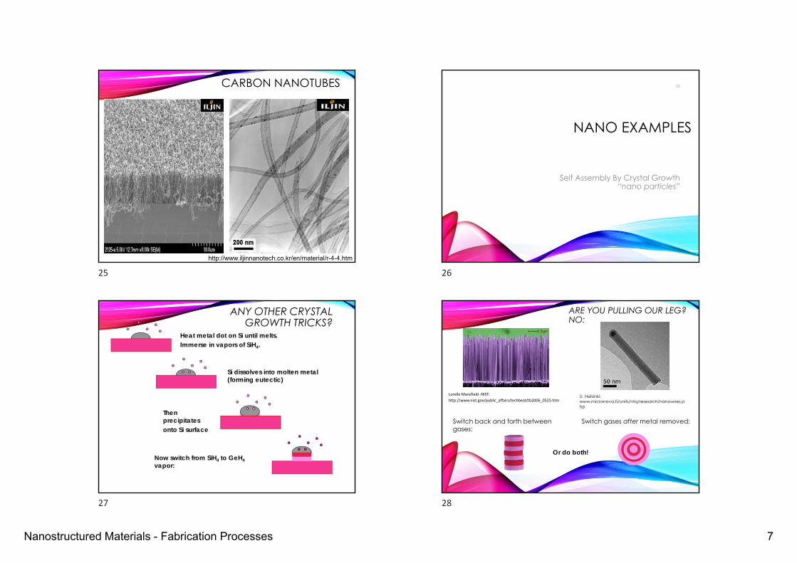
CARBON NANOTUBES
http://www.iljinnanotech.co.kr/en/material/r-4-4.htm
NANO EXAMPLES
Self Assembly By Crystal Growth“nano particles”
26
ANY OTHER CRYSTAL GROWTH TRICKS?
Heat metal dot on Si until melts. Immerse in vapors of SiH4.
Si dissolves into molten metal (forming eutectic)
Then precipitates onto Si surface
Now switch from SiH4 to GeH4vapor:
ARE YOU PULLING OUR LEG? NO:
U. Helsinki: www.micronova.fi/units/ntq/research/nanowires.php
Switch back and forth between gases:
Lorelle Mansfield ‐NIST:http://www.nist.gov/public_affairs/techbeat/tb2006_0525.htm
Switch gases after metal removed:
Or do both!
25 26
27 28

Nanostructured Materials - Fabrication Processes 8
OR HOW ABOUT SELF-ASSEMBLY OF GOLD NANO PARTICLES:
From CytImmuneInc:
Supporting webpage with embedded animation:Lecture 6 - Supporting Materials - CytImmune
IS SELF-ASSEMBLY ALL
ABOUT CRYSTAL GROWTH?
Nano Examples
30
ABSOLUTELY NOT! IN FACT I AM RUNNING OUT OF CRYSTAL GROWTH EXAMPLES
There are more numerous and more powerful examples in the wet worldA small sampler:
Consider the peculiar properties of water:Oxygen wants electrons much more than hydrogen
So charge distribution in water is not uniform - Molecule is "polarized"
O
H H
WHICH MEANS THAT WATER MOLECULES LIKE TO ORGANIZE (SORT OF):
As liquid water jostles about, molecules tend to place (+) hydrogens next to (-) oxygens on neighborEnergy reduced as opposite charges snuggle closer
“HYDROGEN BONDING”(When solidifies, REALLY gets organized - Why it expands)
Screwed up if big non-polarized molecules (e.g. oils) inserted into mix:
Oils hold water molecules apart So oil and water tend to segregate
29 30
31 32

Nanostructured Materials - Fabrication Processes 9
Or even better:
BUT WHAT IF ADD POLARIZED END GROUP TO OIL?
Long molecules organize:
Hydrophillic (water loving) ends aligned in same direction
Becomes the low energy interface with the water
Then water IS attracted to ends:
Excerpt from Letter of Benjamin Franklin to William Brownrigg (Nov. 7, 1773)
...At length being at Clapham, where there is, on the Common, a large Pond ... I fetched out a Cruet of Oil, and dropt a little of it on the Water. I saw it spread itself with surprising Swiftness upon the Surface ... the Oil tho' not more than a Tea Spoonful ... which spread amazingly, and extended itself gradually till it reached the Lee Side, making all that Quarter of the Pond, perhaps half an Acre, as smooth as a Looking Glass....
A nanofilm!
USE IN COMPLEX SELF-ASSEMBLY?
Float layer of oily molecules on top of water bath
Move surface barrier inward to compress oil layer
Monitor surface tension by the pull on a sheet partially immersed in bath to sense when oils "self-assemble" side to side
QuickTime™ and aTIFF (LZW) decompressor
are needed to see this picture.
LANGMUIR FILM
pressuree.g., steric acid
monolayer filmwater
hydrophilic end
hydrophobic end
of an amphiphilicmolecule
33 34
35 36
Nanostructured Materials - Fabrication Processes 10
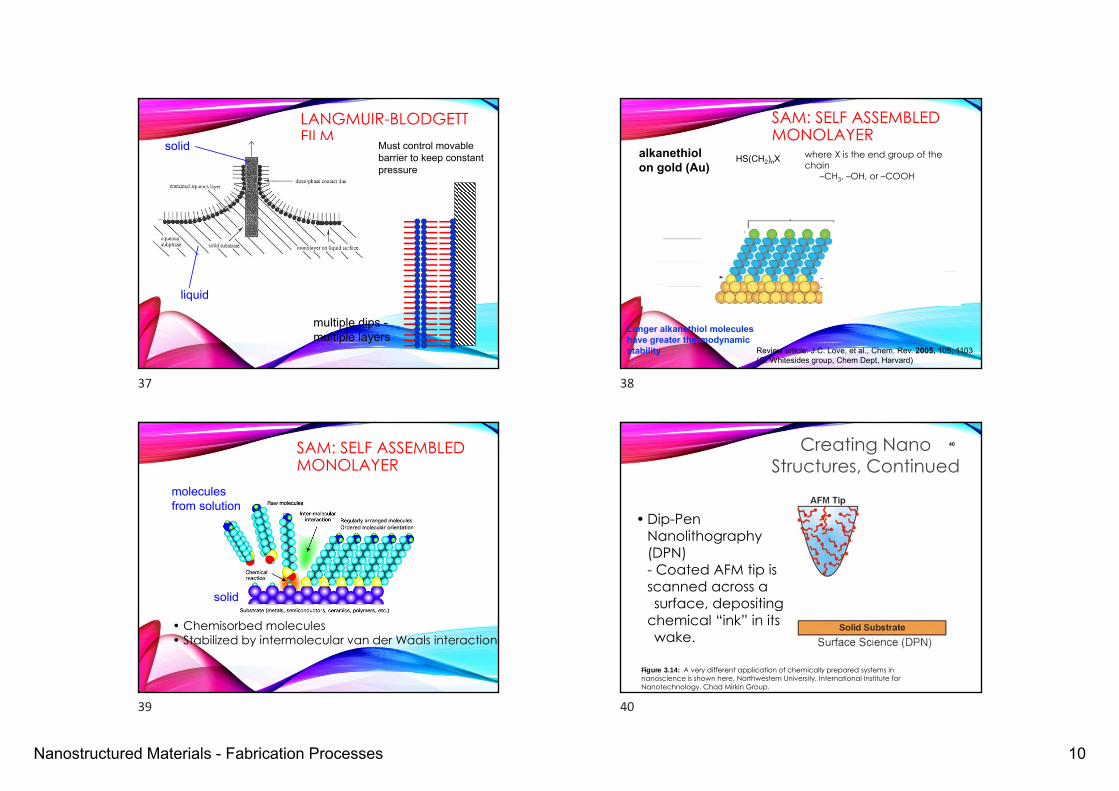
LANGMUIR-BLODGETT FILM
Must control movablebarrier to keep constantpressure
multiple dips -multiple layers
solid
liquid
SAM: SELF ASSEMBLED MONOLAYER
Review article: J.C. Love, et al., Chem. Rev. 2005, 105, 1103(G. Whitesides group, Chem Dept, Harvard)
HS(CH2)nX alkanethiol on gold (Au)
where X is the end group of the chain
–CH3, –OH, or –COOH
Longer alkanethiol molecules have greater thermodynamic stability
SAM: SELF ASSEMBLED MONOLAYER
• Chemisorbed molecules• Stabilized by intermolecular van der Waals interaction
solid
moleculesfrom solution
40
Figure 3.14: A very different application of chemically prepared systems in nanoscience is shown here. Northwestern University, International Institute for Nanotechnology, Chad Mirkin Group.
• Dip-Pen Nanolithography (DPN)- Coated AFM tip is scanned across a surface, depositing
chemical “ink” in its wake.
Creating Nano Structures, Continued
37 38
39 40
Nanostructured Materials - Fabrication Processes 11
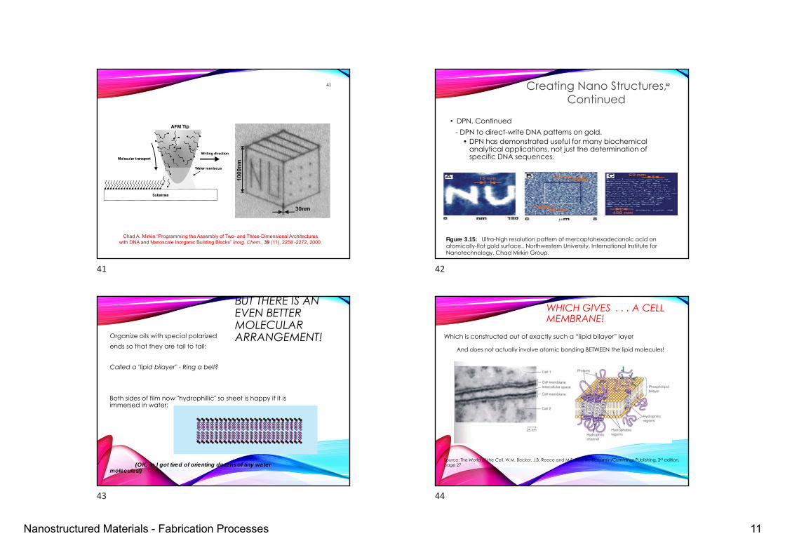
41
Chad A. Mirkin “Programming the Assembly of Two- and Three-Dimensional Architectures with DNA and Nanoscale Inorganic Building Blocks” Inorg. Chem., 39 (11), 2258 -2272, 2000.
• DPN, Continued- DPN to direct-write DNA patterns on gold.
• DPN has demonstrated useful for many biochemical analytical applications, not just the determination of specific DNA sequences.
42
Figure 3.15: Ultra-high resolution pattern of mercaptohexadecanoic acid on atomically-flat gold surface., Northwestern University, International Institute for Nanotechnology, Chad Mirkin Group.
Creating Nano Structures, Continued
BUT THERE IS AN EVEN BETTER MOLECULAR ARRANGEMENT!Organize oils with special polarized
ends so that they are tail to tail:
Called a "lipid bilayer" - Ring a bell?
Both sides of film now "hydrophillic" so sheet is happy if it is immersed in water:
(OK, so I got tired of orienting dozens of tiny water molecules!)
WHICH GIVES . . . A CELL MEMBRANE!
Which is constructed out of exactly such a “lipid bilayer” layer
And does not actually involve atomic bonding BETWEEN the lipid molecules!
Source: The World of the Cell, W.M. Becker, J.B. Reece and M.F. Poenie, Benjamin/Cummings Publishing, 3rd edition, page 27
41 42
43 44
Nanostructured Materials - Fabrication Processes 12
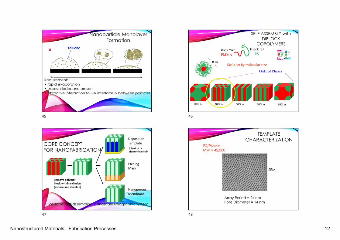
Nanoparticle Monolayer Formation
toluene
Requirements:• rapid evaporation• excess dodecane present• attractive interaction to L-A interface & between particles
SELF ASSEMBLY with DIBLOCK
COPOLYMERSBlock “A” Block “B”
10% A 30% A 50% A 70% A 90% A
~10 nm
Ordered Phases
PMMA PS
Scale set by molecular size
CORE CONCEPT FOR NANOFABRICATION
DepositionTemplate
EtchingMask
NanoporousMembrane
Remove polymerblock within cylinders(expose and develop)
Versatile, self-assembling, nanoscale lithographic system
(physical orelectrochemical)
Array Period = 24 nm Pore Diameter = 14 nm
MW = 42,000PS/PMMA
TEMPLATE CHARACTERIZATION
SEM
45 46
47 48

Nanostructured Materials - Fabrication Processes 13
NANO EXAMPLES
Programmed Assembly
49 PROGRAMMED ASSEMBLY50
Chad A. Mirkin “Programming the Assembly of Two- and Three-Dimensional Architectures with DNA and Nanoscale Inorganic Building Blocks” Inorg. Chem., 39 (11), 2258 -2272, 2000.
PROGRAMMED ASSEMBLY
51
Alexander Kulak, Sean A. Davis, Erik Dujardin, and Stephen Mann “Controlled Assembly of Nanoparticle-
Containing Gold and Silica Microspheres and Silica/Gold Nanocomposite Spheroids with Complex Form” Chem.
Mater., 15 (2), 528 -535, 2003.
BUT THERE IS MUCH MORE THAN MERE ATOMIC/MOLECULAR SELF-ASSEMBLY!
To really get into PROGRAMMED self-assembly we need to learn about:
Organic chemistry → DNA Replication → Et Cetera
49 50
51 52

Nanostructured Materials - Fabrication Processes 14
Using Synthetic DNA for Designer Structures
Ned Seeman, NYU
Designer DNA molecules can be synthesized chemically, and allowed to assemble into a specific configuration of lowest energy.
Programmed DNA Folding to Make "DNA Origami"
P.W.K. Rothemund, Nature 440, 297 (2006)
How do we get to these levels of complexity?
55
“PROGRAMMED” SELF-ASSEMBLY
56
53 54
55 56

Nanostructured Materials - Fabrication Processes 15
The structure of the parts must encode the structure of the whole
Components need to be complexDesign and fabrication may this be difficult
Partitioned by complex internal interfaces
They have no operational feature
Unless strengthened after assembly, they will be weak
Major constraints
Fundamental Advanatage over mechanically directed assembly
Requires no machineryRandom Brownian motion does the job
Can be used to produce atomically precise nanosystems
Billions of themBy the tonneEstablishing a wide-ranging based technology
Biomolecular fabrication based on programmable machines
Produce complex parts necessary for self assembly of complex systems.Can use artificial biomolecular machines, and then non biomolecular, to produce better and more diverse engineering materials.
CREDITS / ACKNOWLEDGEMENTS
Some of the notes are from a lecture series authored by John C. Bean who also created all figures not explicitly credited.
Many of those figures (and much of the material to be used for this class) are drawn from the "UVA Virtual Lab" (www.virlab.virginia.edu) website developed under earlier NSF grants.
Copyright John C. Bean (2012)
(However, permission is granted for use by individual instructors in non-profit academic institutions)
57 58
59