1. Distortion in Nonlinear Systemslong/ece145a/Performance_Limitations.pdf · ECE145A/ECE218A...
32
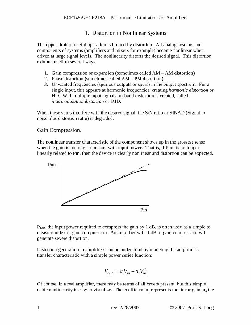
ECE145A/ECE218A Performance Limitations of Amplifiers 1. Distortion in Nonlinear Systems The upper limit of useful operation is limited by distortion. All analog systems and components of systems (amplifiers and mixers for example) become nonlinear when driven at large signal levels. The nonlinearity distorts the desired signal. This distortion exhibits itself in several ways: 1. Gain compression or expansion (sometimes called AM – AM distortion) 2. Phase distortion (sometimes called AM – PM distortion) 3. Unwanted frequencies (spurious outputs or spurs) in the output spectrum. For a single input, this appears at harmonic frequencies, creating harmonic distortion or HD. With multiple input signals, in-band distortion is created, called intermodulation distortion or IMD. When these spurs interfere with the desired signal, the S/N ratio or SINAD (Signal to noise plus distortion ratio) is degraded. Gain Compression. The nonlinear transfer characteristic of the component shows up in the grossest sense when the gain is no longer constant with input power. That is, if Pout is no longer linearly related to Pin, then the device is clearly nonlinear and distortion can be expected. Pout Pin P 1dB , the input power required to compress the gain by 1 dB, is often used as a simple to measure index of gain compression. An amplifier with 1 dB of gain compression will generate severe distortion. Distortion generation in amplifiers can be understood by modeling the amplifier’s transfer characteristic with a simple power series function: 3 1 3 out in in V aV aV = − Of course, in a real amplifier, there may be terms of all orders present, but this simple cubic nonlinearity is easy to visualize. The coefficient a 1 represents the linear gain; a 3 the 1 rev. 2/28/2007 © 2007 Prof. S. Long
Transcript of 1. Distortion in Nonlinear Systemslong/ece145a/Performance_Limitations.pdf · ECE145A/ECE218A...
ECE145A/ECE218A Performance Limitations of Amplifiers
1. Distortion in Nonlinear Systems The upper limit of useful operation is limited by distortion. All analog systems and components of systems (amplifiers and mixers for example) become nonlinear when driven at large signal levels. The nonlinearity distorts the desired signal. This distortion exhibits itself in several ways:
1. Gain compression or expansion (sometimes called AM – AM distortion) 2. Phase distortion (sometimes called AM – PM distortion) 3. Unwanted frequencies (spurious outputs or spurs) in the output spectrum. For a
single input, this appears at harmonic frequencies, creating harmonic distortion or HD. With multiple input signals, in-band distortion is created, called intermodulation distortion or IMD.
When these spurs interfere with the desired signal, the S/N ratio or SINAD (Signal to noise plus distortion ratio) is degraded. Gain Compression. The nonlinear transfer characteristic of the component shows up in the grossest sense when the gain is no longer constant with input power. That is, if Pout is no longer linearly related to Pin, then the device is clearly nonlinear and distortion can be expected. Pout Pin P1dB, the input power required to compress the gain by 1 dB, is often used as a simple to measure index of gain compression. An amplifier with 1 dB of gain compression will generate severe distortion. Distortion generation in amplifiers can be understood by modeling the amplifier’s transfer characteristic with a simple power series function:
31 3out in inV a V a V= −
Of course, in a real amplifier, there may be terms of all orders present, but this simple cubic nonlinearity is easy to visualize. The coefficient a1 represents the linear gain; a3 the
1 rev. 2/28/2007 © 2007 Prof. S. Long

ECE145A/ECE218A Performance Limitations of Amplifiers
distortion. When the input is small, the cubic term can be very small. At high input levels, much nonlinearity is present. This leads to gain compression among other undesirable things. Suppose an input Vin =A sin (ωt) is applied to the input.
233
1 33 1sin( ) sin(3 )
4 4outa AV A a t a A tω ω
⎡ ⎤= − +⎢ ⎥
⎣ ⎦
Gain Compression Third Order Distortion Gain compression is a useful index of distortion generation. It is specified in terms of an input power level (or peak voltage) at which the small signal conversion gain drops off by 1 dB. The example above assumes that a simple cubic function represents the nonlinearity of the signal path. When we substitute Vin(t) = A sin (ωt) and use trig identities, we see a term that will produce gain compression: A(a1 - 3a3A
2/4). If we knew the coefficient a3, we could predict the 1 dB compression input voltage. Typically, we obtain this by measurement of gain vs. input voltage. Harmonic Distortion We also see a cubic term that represents the third-order harmonic distortion (HD) that also is caused by the nonlinearity of the signal path. Harmonic distortion is easily removed by filtering; it is the intermodulation distortion that results from multiple signals that is far more troublesome to deal with. Note that in this simple example, the fundamental is proportional to A whereas the third-order HD is proportional to A3. Thus, if Pout vs. Pin were plotted on a dBm scale, the HD power will increase at 3 times the rate that the fundamental power increases with input power. This is often referred to as being “well behaved”, although given the choice, we could easily live without this kind of behavior!
2 rev. 2/28/2007 © 2007 Prof. S. Long

ECE145A/ECE218A Performance Limitations of Amplifiers
Intermodulation Distortion Let’s consider again the simple cubic nonlinearity a3vin3. When two inputs at ω1 and ω2
are applied simultaneously to the RF input of the mixer, the cubing produces many terms, some at the harmonics and some at the IMD frequency pairs. The trig identities show us the origin of these nonidealities. [4]
We will be mainly concerned with the third-order IMD. (actually, any distortion terms can create in-band signals – we will discuss this later). IMD is especially troublesome since it can occur at frequencies within the signal bandwidth. For example, suppose we have 2 input frequencies at 899.990 and 900.010 MHz. Third order products at 2f1 - f2 and 2f2 - f1 will be generated at 899.980 and 900.020 MHz. These IM products may fall within the filter bandwidth of the system and thus cause interference to a desired signal. The spectrum would look like this, where you can see both third and fifth order IM.
3 rev. 2/28/2007 © 2007 Prof. S. Long

ECE145A/ECE218A Performance Limitations of Amplifiers
P1
IIP3Pin (dBm)
fundamental
third-order IMD
PIMD
Pout (dBm)
PIN
OIP3x
2x
P1
IIP3Pin (dBm)
fundamental
third-order IMD
PIMD
Pout (dBm)
PIN
OIP3x
2x
( )3 112IN IMDIIP P P P= + −
IMD power, just as HD power, will have a slope of 3 on a Pout vs Pin (dBm) plot. A
input
IP3. d
is common practice to extrapolate or calculate the intercept point from data taken at
OIP3 = (P1 − PIMD)/2 + P1
lso, the input and output intercepts (in dBm) are simply related by the gain (in dB):
OIP3 = IIP3 + power gain.
ther higher odd-order IMD products, such as 5th and 7th, are also of interest, and can
widely-used figure of merit for IMD is the third-order intercept (TOI) point. This is afictitious signal level at which the fundamental and third-order product terms would intersect. In reality, the intercept power is 10 to 15 dBm higher than the P1dB gain compression power, so the circuit does not amplify or operate correctly at the IIP3 level. The higher the TOI, the better the large signal capability of the system. If specified in terms of input power, the intercept is called IIP3. Or, at the output, OThis power level can’t be actually reached in any practical amplifier, but it is a calculatefigure of merit for the large-signal handling capability of any RF system.
level. The higher the TOI, the better the large signal capability of the system. If specified in terms of input power, the intercept is called IIP3. Or, at the output, OThis power level can’t be actually reached in any practical amplifier, but it is a calculatefigure of merit for the large-signal handling capability of any RF system. ItItleast 10 dBm below P1dB. One should check the slopes to verify that the data obeys theexpected slope = 1 or slope = 3 behavior. The TOI can be calculated from the followinggeometric relationship:
least 10 dBm below P1dB. One should check the slopes to verify that the data obeys theexpected slope = 1 or slope = 3 behavior. The TOI can be calculated from the followinggeometric relationship: AA OOalso be defined in a similar way, but may be less reliably predicted in simulations unlessthe device model is precise enough to give accurate nonlinearity in the transfer characteristics up to the 2n-1th order. also be defined in a similar way, but may be less reliably predicted in simulations unlessthe device model is precise enough to give accurate nonlinearity in the transfer characteristics up to the 2n-1th order.
4 rev. 2/28/2007 © 2007 Prof. S. Long

ECE145A/ECE218A Performance Limitations of Amplifiers
Cross Modulation In addition, the cross-modulation effect can also be seen in the equation above. The amplitude of one signal (say ω1) influences the amplitude of the desired signal at ω2 through the coefficient 3V12V2a3/2. A slowly varying modulation envelope on V1 will cause the envelope of the desired signal output at ω2 to vary as well since this fundamental term created by the cubic nonlinearity will add to the linear fundamental term. This cross-modulation can have annoying or error generating effects at the output. Second Order Nonlinearity In the simplified model above, we have neglected second order nonlinear terms in the series expansion. In many cases, an amplifier or other RF system will have some even-order distortion as well. The transfer function then would look like this:
2 31 2 3out in in inV a V a V a V= + +
If we once again apply two signals at frequencies ω1 and ω2 to the input, we obtain:
2 22 2 1 1 2 2 1 2 1 2sin ( ) sin ( ) 2 sin( )sin( )outV a V t V t VV t tω ω ω⎡ ⎤= + +⎣ ⎦ω
The sin2 terms expand into:
[ ] [ ]2 22 1 1 2 2 2
1 11 cos(2 ) 1 cos(2 )2 2
a V t a V tω ω− + −
From this, we can see that there is a DC term and a second harmonic term present for each input. The DC term is proportional to the square of the voltage, therefore power. This is one use of second-order nonlinearity – as a power sensor. The HD term is also proportional to the square of the voltage. Thus, on a power out vs. power in plot, it has a slope of 2.
5 rev. 2/28/2007 © 2007 Prof. S. Long

ECE145A/ECE218A Performance Limitations of Amplifiers
When the next term is expanded, the product of two sine waves is seen to produce the sum and difference frequencies.
[ ]2 1 2 2 1 2 1cos( ) cos( )a V V t tω ω ω ω− − + This can be both a useful property and a problem. The useful application is as a frequency translation device, often called a mixer, a downconverter, or an upconverter. The desired output is selected by inserting a filter at the output of the device. Second order distortion, if generated by out-of-band signals, can also lead to interference in-band as shown below. Preselection filtering can generally suppress this in narrowband amplifiers, but it can be a big problem for wideband circuits. A SOI, or second-order intercept can also be defined as shown below:
he second-order IMD slope = 2. IIP2 can be calculated from measurement by:
IIP2 = Pin + P1 – PIMD
OIP2 = IIP2 + Power Gain = 2 P1 - PIMD
wo tone simulation in ADS nic Balance Simulation Tutorial on the course web
P1
IIP2Pin (dBm)
fundamental
second-order IMDPIMD
Pout (dBm)
Pin
OIP2x
xP1
IIP2Pin (dBm)
fundamental
second-order IMDPIMD
Pout (dBm)
Pin
OIP2x
x
T
TRefer to the first part of the Harmopage.
6 rev. 2/28/2007 © 2007 Prof. S. Long

ECE145A/ECE218A Performance Limitations of Amplifiers
How is the Intercept Point affected by cascaded stages?
ains multiply in a cascade: PO = Pi G1 G2 G3 (or add them if in dB)
dividual intercept points must be referred to the same reference plane. It can be either
. The third order intercept
PiIIP = ?
G1OIP1
G2OIP2
G3OIP3
POOIP = ?
PiIIP = ?
G1OIP1
G2OIP2
G3OIP3
POOIP = ?
G
In
at the input or the output. In this example, the output IP, OIP, is specified for each stage.
1. Convert all OIPs from dBm to mW and gains from dB to a power ratio.
2. Let’s refer all of these OIPs to the output plane.
OIP3
G3 OIP2
G2 G3 OIP1
3 cascading relationship is:
321
31
23111
+=132
GGGOIPIIP
OIPOIPGOIPGGOIP
=
+
4. Convert the results back to dBm if desired.
7 rev. 2/28/2007 © 2007 Prof. S. Long

ECE145A/ECE218A Performance Limitations of Amplifiers
Second order intercept cascading is accomplished by the following equations:
321
31
231
13211
GGGOIPIIP
OIPOIPGOIPGGOIP
=
++=
Example: Receiver Front End
PiIIP = ?
G1 = 10 dBOIP1 = 0 dBm
G2 = 0 dBOIP2 = 20 dBm
POOIP = ?
PiIIP = ?
G1 = 10 dBOIP1 = 0 dBm
G2 = 0 dBOIP2 = 20 dBm
POOIP = ?
1. Convert dBm to mW: OIP1 = 1 mW, OIP2 = 100 mW
Convert dB to a power ratio: G1 = 10, G2 = 1
2. Refer to the output plane:
1/OIP = 1 + 1/100 = 1.01 OIP = 1 (0 dBm)
3. IIP = OIP/10 = 0.1 (-10 dBm)
We can see that the LNA completely dominates the IIP in this example. IF we eliminated
the LNA, then OIP = OIP2 = 20 dBm and IIP = 20 dBm, a 30 dB improvement!
What do we lose by eliminating the LNA?
8 rev. 2/28/2007 © 2007 Prof. S. Long

ECE145A/ECE218A Performance Limitations of Amplifiers
2. Next Topic: NOISE
Noise determines the minimum signal power (minimum detectable signal or MDS) at the input of the system required to obtain a signal to noise ratio of 1. A S/N = 1 is usually considered to be the lower acceptable limit except in systems where signal averaging or processing gain is used. Noise figure is a figure of merit used to describe the amount of degradation in S/N ratio that the system introduces as the signal passes through. For some applications, the minimum signal power that is detectable is
important.
o Satellite receiver
o Terrestrial microwave links
o 802.11
Noise limits the minimum signal that can be detected for a given signal input
power from the source or antenna.
We will identify sources of noise, and define related quantities of interest:
o S/N = Signal to noise ratio
o MDS = Minimum Detectable Signal
o F = Noise factor
o NF = 10 * log(F) = Noise figure
9 rev. 2/28/2007 © 2007 Prof. S. Long

ECE145A/ECE218A Performance Limitations of Amplifiers
Noise Basics: What is noise? How is it evident to us? Why is it important?
hat:
Any unwanted random disturbance
urrent. Frequency and phase
ed by a Gaussian probability
he cumulative area under the curve represents the probability of the event
ecause of the random process, the average value is zero:
vn
t P
vnvn
t P
vn
W
1.
2. Random carrier motion produces a c
are not predictable at any instant in time
3. The noise amplitude is often represent
density function.
T
occurring. Total area is normalized to 1.
B
[ ] 0)(1 1 +Tt
1
lim =∫=∞→
dttvT
vt
nT
n
e cannot predict vn(t), but the variance (standard deviation) is finite: W
10 rev. 2/28/2007 © 2007 Prof. S. Long

ECE145A/ECE218A Performance Limitations of Amplifiers
[ ] 22
2 1
1
)(1lim σ=∫=
+
∞→dttv
Tv
Tt
tn
Tn
Often we refer to the rms value of the noise voltage or current:
2
, nrmsn vv =
Sources of Noise in Circuits:
o Shot noise forward-biased junctions
o Thermal Noise any resistor
o Flicker (1/f) noise trapping effects
Shot noise: This is due to the random carrier flow across a pn junction.
Electrons and holes randomly diffuse across the junction producing noise
current pulses that occur randomly in time. The steady state current
measured across a forward biased diode junction is really a large number of
discrete current pulses.
p
ID I
The variance of this current:
( ) 22
0
2 1lim σ=∫ −=
∞→dtII
Ti
TD
T
It can be shown that this mean square noise current can be predicted by
BqIi D22 =
11 rev. 2/28/2007 © 2007 Prof. S. Long

ECE145A/ECE218A Performance Limitations of Amplifiers
where
q = charge of an electron = 1.6 x 10⁻¹⁹
ID = diode current
B = bandwidth in Hertz (sometimes called Δf)
The noise current spectral density: DqIBi 2/2 =
o Independent of frequency (white noise)
o Independent of temperature for a fixed current
o Proportional to the forward bias current
o Gaussian probability distribution
1 mA of current corresponds to a noise current spectral density of
18 pA/√Hz
read: 18 picoamp per root Hertz
Thermal Noise: Thermal noise, sometimes called Johnson noise, is due to
random motion of electrons in conductors. It is unaffected by DC current
and exists in all conductors. Its spectral density is also frequency
independent, but is directly proportional to temperature. The noise
probability density is Gaussian.
kTRBv 42=
RkTBi /42=
4kT = 1.66 x 10 –20 V-C
12 rev. 2/28/2007 © 2007 Prof. S. Long

ECE145A/ECE218A Performance Limitations of Amplifiers
A 50 ohm resistor produces a noise voltage spectral density of
0.9 nV/√Hz
or a Norton equivalent noise current spectral density of
18 pA/√Hz
Flicker or 1/f noise. This noise source is most evident at very low
frequencies. It is hard to localize its physical mechanisms in most devices.
There is usually some 1/f noise contribution due to charge traps with long
time constants. The trap charge then is randomly released after some
relatively long period of time. 1/f noise is modeled by:
fIKBi =/2
K is a fudge factor. It can vary wildly from one type of transistor to
the next or even from one fabrication lot to the next.
I is the current flowing through the device.
B is the bandwidth.
Corner frequency
Log (i2/B)
Log f
1/f noise can be described by a corner frequency.
Carbon resistors exhibit 1/f noise; metal film resistors do not.
13 rev. 2/28/2007 © 2007 Prof. S. Long

ECE145A/ECE218A Performance Limitations of Amplifiers
Noise can be modeled as a Thevenin equivalent voltage source or a Norton
equivalent current source. The noise contributed by the resistor is modeled
by the source, thus the resistor is considered noiseless.
is important to note that noise sources:
ow is just to distinguish current
o ebraically, but as RMS sums
R
vnin R
R
vnin R
It
o Do not have polarity (the arr
from voltage)
Do not add alg
2122
, 44kTBRvv +=+= 212 kTBRv nntotaln
If the sources are correlated (derived from the same physical noise source),
en there is an additional term:
R2vn2
th
2121, nnnntotaln
C can vary between –1 and 1.
222 2 vCvvvv ++=
R1vn1R2vn2R1vn1
14 rev. 2/28/2007 © 2007 Prof. S. Long

ECE145A/ECE218A Performance Limitations of Amplifiers
The available noise power can be calculated from the RMS noise voltage or
current:
kTBRiR
vP nnav ===
22
44
That is, the av
o
o
-21 watt
noise room temperature of 290 K. If
converted to dBm = 10 log(P/10-3
e are generally interested in the noise power in other bandwidths than 1 Hz. It’s easy
to calculate: P = kTB
= -144 dBm
ailable noise power from the source is
independent of resistance
proportional to temperature
o proportional to bandwidth
o has no frequency dependence
Pav = 4 x 10
in a 1 Hz bandwidth at the standard
), this power becomes
- 174 dBm/Hz
W
where kT = -174 dBm
To convert bandwidth in Hertz to dB: 10 log B
EX: Suppose your B = 1000 Hz. P = kTB.
In dBm, P = -174 + 10 log (1000) = -174 + 30
15 rev. 2/28/2007 © 2007 Prof. S. Long

ECE145A/ECE218A Performance Limitations of Amplifiers
Can a resistor produce infinite noise voltage?
Vn2 = 4kTBR
Equivalent circuit for noisy resistor.
Always some shunt capacitance.
l noise power:
R
to find tota Vno2df =
kTC
= Vno2
0
∞
∫
R total noise power is independent of
Low Pass
Vno = Vn1
1+ ω2C2R2
9R
4R
R
f
log10 Vno
VnoCVn
16 rev. 2/28/2007 © 2007 Prof. S. Long

ECE145A/ECE218A Performance Limitations of Amplifiers
Noise Equivalent Bandwidth An amplifier or filter has a nonideal frequency response. Noise power transmitted
through is determined by the bandwidth.
Noise power ∝ (mean square voltage) – white noise V 2
v i2 A f( )2
= v o2 / Hz in a 1Hz interval
Summation over entire frequency band
v o2 f( )df =
o
∞
∫ v i2 A f( )2
dfo
∞
∫
We choose an equivalent BW, B, with rectangular profile whose area is the same.
Am2 B = A f( )2
dfo
∞
∫
B =1
Am2 A f( )2
dfo
∞
∫
This is the definition of bandwidth that we will assume in subsequent
calculations.
A f( )2
AM2
f B
A f( ) v i2
v o2
17 rev. 2/28/2007 © 2007 Prof. S. Long

ECE145A/ECE218A Performance Limitations of Amplifiers
Signal-to-noise ratio Several definitions
SNR =PS
PN
=SN
generally use available power
Pav =VS
2
4Rrms voltage V S
RVS +-
S + N
N and S + N + D
N or SINAD are alternate definitions.
Why is S/N important?
Affects the error rate when receiving information.
Ref: S. Haykin, Communication Systems, 4th ed., Wiley, 2001
18 rev. 2/28/2007 © 2007 Prof. S. Long

ECE145A/ECE218A Performance Limitations of Amplifiers
Noise Factor, F:
is a measure of how much noise is added by a component such as an
amplifier.
F =Si / Ni
So / No
>1
because S/N at input will always be greater than S/N at output, F > 1.
Noise factor represents the extent that S/N is degraded by the system.
F = total noise power available at outputnoise power available at output due to source @ 290k
=Navo
Navi ⋅ Gav
Gav = Savo
Savi
F =S / N( )avi
S / N( )avo
Noise Figure: NF =10 log10 F
S Ni , So, NoGai
source at 290K
The higher the noise factor (or noise figure), the larger the degradation of S/N by the amplifier.
19 rev. 2/28/2007 © 2007 Prof. S. Long

ECE145A/ECE218A Performance Limitations of Amplifiers
Ex.
Gav =10dBNF = 3dB
B =106 Hz amplifier specification
signal available power
dBmWRvS
s
savi 113105
400102
815
122−=×=
×== −
−
signal av. pwr. = Savi =vs
2
4RS
=10−12
200= 5 × 10¹⁵ N ⇒ −113dBm
noise av. pwr. = Navi = kTB = −174 + 60 = −114dBm
VS = 1μV
RS = 50ΩGav
RL
So / No( )=Si / Ni
F
+ -
W
vS = 1.4 μV
Since noise power increases with B
10 log10 B = 60dB (in this example)
10 logSavo
Navo
⎛ ⎝ ⎜
⎞ ⎠ ⎟ =10 log
Savi
Navi
⎛ ⎝ ⎜
⎞ ⎠ ⎟ − NF
= −113 − −114( )− 3=1dB −3dB = −2dB (not very good)
How can So / No be improved?
1. Reduce F. Slight room for improvement
2. Reduce B. Major improvement if application can tolerate
reduced B.
3. Increase antenna gain. Lots of room for improving Si/Ni
20 rev. 2/28/2007 © 2007 Prof. S. Long

ECE145A/ECE218A Performance Limitations of Amplifiers
say B = 105
Navi = −174 + 50 = −124dBmSavi
Navi
= 11dB and Savo
Navo
= 8dB
Ex. Noise Floor of Spectrum Analyzer
typical NF ≅ 25dB for SA . NAVO = NAVI ⋅ F ⋅ GAV
N AVI = −174dBm / Hz( )+ 10 log B
NF = 25dB resolution bandwidth (RBW)
GAV =1 0dB( )
RBW NAVO
1kHz10kHz100kHz
etc.
−119 dBm−109−99
We will see later how this can be improved.
21 rev. 2/28/2007 © 2007 Prof. S. Long

ECE145A/ECE218A Performance Limitations of Amplifiers
The excess noise added by an active circuit such as an amplifier can also be
modeled by an extra resistor at an effective input noise temperature, Te .
PG OUT
Pav = kTo B noisy amp
is equivalent to:
G POUT = k To + Te( )B ⋅ G
kTeBPav (useful when To ≠ 290k )
noiseless Σ
In terms of noise factor:
F =noise out due to DUT + noise out due to source
Noise out due to source
= kTeBG + kToBGkToBG
= 1+ Te
To
or T e = 290 F − 1( )
(where F is a number, not dB)
22 rev. 2/28/2007 © 2007 Prof. S. Long

ECE145A/ECE218A Performance Limitations of Amplifiers
Significance of Te: excess noise.
Navo total( ) = kBG To + Te( )
due to source resistor
due to amplifier
Example: NF =1dB ⇒ F = 1.26 = 1 + Te To =1 + Te 290
so Te = 75K
total output noise ⇒ 290 + 75 = 365K equivalent source temp
So what? Not major increase in noise power. Further reduction
in F may not be justified.
But, for space application: To = 20K is possible.
Then T = To + Te = 20 + 75 = 95K
major degradation in noise temp.
F or NF at room temperature doesn’t reveal this so
clearly.
F = 1 + 75/20 = 4.5 (NF = 7 dB)
23 rev. 2/28/2007 © 2007 Prof. S. Long

ECE145A/ECE218A Performance Limitations of Amplifiers
Noise Figure of Cascaded Stages. Use Available gain.
Why available gain?
Noise power defined as available power. Cascading of noise is more convenient
when GA is used.
Second Stage Noise Contribution
G1 G2
Ni = kToB No1 No2
F1 F2
T1 = eff. noise temp@ input
T2
RS
No1 = k To + T1( )BG1
No2 = k To + T1( )BG1G2 + kT2BG2
To get total input referred noise power: No2
G1G2
= Ni (equivalent) = k To + T1( )B + kT2B / G1
excess noise at input:
kT1B+ kT2 B / G1
Recall that F = 1 +Te
To
Te = T1 + T2 G1
FTOTAL = 1 +T1
To
F1
+
T2
ToG1
F2 −1G1
+
Third Stage:
+F3 − 1G1G2
24 rev. 2/28/2007 © 2007 Prof. S. Long

ECE145A/ECE218A Performance Limitations of Amplifiers
Noise Figure of Cascaded Stages
S N( )IN F1
G1
F2
G2
F3
G3
S N( )OUT
Fi = Noise Factor
G i = Available Gain⎫ ⎬ ⎭
not in dB
FTOTAL = F1 + F2 −1G1
+ F3 −1G1G2
+ ...
= Input Total Noise Factor
S N( )IN
S N( )OUT
= FTOTAL
Or: S N( )OUT dB = S N( )IN dB − NFTOTAL
25 rev. 2/28/2007 © 2007 Prof. S. Long

ECE145A/ECE218A Performance Limitations of Amplifiers
Additional stages in the cascade treated the same way.
Total available gain of cascade = Ga1 Ga2 Ga3...
1. If noise figure is important in a receiver, it is standard procedure to design so
that the first stage sets the noise performance.
FTOTAL = F1 +F2 −1
G1
+F3 −1G1G2
This will require a large enough G to diminish the noise contribution of the
second stage. 1
2. How is the minimum detectable signal or MDS defined?
* at a given B (very important)
PMDS ⇒S + N
N= 3dB or S = N
SN
= O dB
( )10log( )MDSP kTB NF dB= +
OR
174 / 10log ( )MDSP dBm Hz B NF dB= − + +
26 rev. 2/28/2007 © 2007 Prof. S. Long

ECE145A/ECE218A Performance Limitations of Amplifiers
Noise figure of Passive Networks ex. attenuator
filter
matching network
No active components. Only resistors and reactances.
no excess noise is generated by network Savo
Savi
= Gav
so, S N( )i =PS
kTo B
S N( )o =G ⋅ PS
kToB
F =S N( )i
S N( )o
=1G
Noise factor is just the inverse of gain.
or, NF = −G dB( )
ex. 10dB attenuator Gav = −10dB
NF =10dB
passive network Gav
F
ZS
PS
Navi = kToB Navo = kTo B
27 rev. 2/28/2007 © 2007 Prof. S. Long

ECE145A/ECE218A Performance Limitations of Amplifiers
Measure noise figure of amplifier. Method #1: Use the spectrum analyzer as a noise receiver.
B = 106 HzG1 =10dB
F1 = 2dB
1.58( )
B very wideF2 = 30dB
1000( )
Spect. Analyzer
DUTAMP
50 ohms
FTOTAL = 1.58 +99910
= 101.5 20dB( )
completely dominated by second stage.
Now add preamp ahead of SA.
( )
1
1
102
1.58
G dF d
BB
==
( )
2
2
301
1.26
G dF d
BB
== 3 30F d=
Spect. Analyzer
Pre Amp
DUTAMP
50 ohms
B
( )( )( )
( )
1.26 1 9991.58 1.7110 10 1000
2.3
TOTALF
dB
−= + + =
With preamp, SA noise contribution can be kept small enough that
front end noise figure can be determined with accuracy. Otherwise,
rather hopeless.
28 rev. 2/28/2007 © 2007 Prof. S. Long

ECE145A/ECE218A Performance Limitations of Amplifiers
Measuring NF. Method #2
Use a calibrated signal source, matched correctly to amp under test.
can measure
Vrms across
known RL
SIG GEN DUT
Power MeterPS
F1,G1, B1B2
G2BPF
* B2 << B1
Noise equiv. BW
set by BPF
Two measurements
1. Generator inactive, but still properly terminating amp. Must have
correct source impedance.
1S avs avi oP P N kT B= = =
P1 = output noise power from chain ← measurement 1= FkTo AtB2
total F transducer gain =Power delivered to load
Power available from source
2. Generator on. PS =VS
2
8RS
available power from generator in excess of kTB
P2 = FkTo AtB2 + PS At ← measurement 2
Eliminate : At F =1
P2 P1 − 1⋅
PS
kToB2
Y ≡P2
P1
29 rev. 2/28/2007 © 2007 Prof. S. Long

ECE145A/ECE218A Performance Limitations of Amplifiers
Method #3: HOT-COLD NF
You can also use a calibrated noise source for measuring NF.
LNA50Ω noise source
Power Meter
B1 B2
B3 > B2
DUT preamp
1 2nB B B>> <
The advantage here is that we don’t need to know noise equivalent BW
accurately.
Noise source has very wide BW compared with system under test.
PH = noise power with source on = kTH B
TH = effective noise temp. of source
Po = kTo B = noise power with source off.
To = 290k
P P T−Excess Noise Ratio = ENR = H o
Po
H
To
−1=
ENR dB( )= 10 log10TH
To
−1⎛ ⎝ ⎜
⎞ ⎠ ⎟
Y factor for noise source:
YS =PH
Po=
TH
To
30 rev. 2/28/2007 © 2007 Prof. S. Long

ECE145A/ECE218A Performance Limitations of Amplifiers
So, we can use the noise source instead of the signal generator.
1. Source off. Noise power at meter: P1 = F kToB AT
total noise factor transducer gain
2. Source on.
Ts BAkTYPP 012 +=
Divide: P2
P1= Y = 1+
YS
F
again, the transducer gain cancels, and now B cancels too. We can solve for F
from the measured P2 P1 .
F =YS
Y −1 Noise factor – numerical ratios, not dB.
and
NF =10 log F dB( )
31 rev. 2/28/2007 © 2007 Prof. S. Long

ECE145A/ECE218A Performance Limitations of Amplifiers
The tunable noise figure meter is a receiver. The mixer block upconverts the input noise
signal to a 2 GHz power meter. 2in LOf GHz f= −
Thus, by choosing the local oscillator frequency fLO, we measure the noise power within
the bandwidth of the IF filter. The noise figure meter also applies a square wave to turn
the noise source on and off, obtaining the HOT/COLD input noise condition needed to
determine F. As an added bonus, the meter also measures the gain of the device under
test.
32 rev. 2/28/2007 © 2007 Prof. S. Long