1 DATA AND CONTROL SUBSYSTEMS COMPONENTS …web.cs.ucla.edu/Logic_Design/SLPDF/ch14.pdf ·...
66
1 DATA AND CONTROL SUBSYSTEMS • COMPONENTS AND ORGANIZATION OF DATA SUBSYSTEM • DESIGN OF DATA SUBSYSTEM • IMPLEMENTATION OF CONTROL SUBSYSTEM AS A SEQUENTIAL MA- CHINE • SPECIFICATION AND IMPLEMENTATION OF A MICROPROGRAMMED CONTROLLER Introduction to Digital Systems 14 – Data and Control Subsystems
Transcript of 1 DATA AND CONTROL SUBSYSTEMS COMPONENTS …web.cs.ucla.edu/Logic_Design/SLPDF/ch14.pdf ·...

1
DATA AND CONTROL SUBSYSTEMS
• COMPONENTS AND ORGANIZATION OF DATA SUBSYSTEM
• DESIGN OF DATA SUBSYSTEM
• IMPLEMENTATION OF CONTROL SUBSYSTEM AS A SEQUENTIAL MA-CHINE
• SPECIFICATION AND IMPLEMENTATION OF A MICROPROGRAMMEDCONTROLLER
Introduction to Digital Systems 14 – Data and Control Subsystems

2
DATA SUBSYSTEM
i) STORAGE MODULES
ii) FUNCTIONAL MODULES (operators)
iii) DATAPATHS (switches and wires)
iv) CONTROL POINTS
v) CONDITION POINTS
Introduction to Digital Systems 14 – Data and Control Subsystems

3
Z
ld_conds
CK
Conditions:
RegisterR_CONDS
c_31
c_30
(0..0)
ovf zerosigncout
ovf zerosigncout
ALU
SHIFTER
c_0
cmpl_L CMPL_L
MUX_L
CMPL_R cmpl_R
MUX_R
REGISTER ARRAYR
4
44
2
ld_ADDR
CK
LDR_ADDR
ld_DATA
CK
LDR_DATA
sh_left
sh_right
read_addr_R
read_addr_L
write
write-addr
DATA_IN
cmux_L cmux_R
R_ADDR R_DATA
4alu_opcode
S-BUS
32-bit wide connections
Figure 14.1: EXAMPLE OF A DATA SUBSYSTEM.
Introduction to Digital Systems 14 – Data and Control Subsystems

4
STORAGE MODULES
• INDIVIDUAL REGISTERS, with separate connections and controls;
• ARRAYS OF REGISTERS, sharing connections and controls;
• REGISTER FILE
• RANDOM-ACCESS MEMORY (RAM)
• COMBINATION OF INDIVIDUAL REGISTERS AND ARRAYS OF REGIS-TERS.
Introduction to Digital Systems 14 – Data and Control Subsystems

5
REGISTER FILE
RegisterFile
n n
Wr
RAr
WA
Zl Zr
RAl
n
k
k k
X
clk
Figure 14.2: REGISTER FILE
USE WORK.BitDefs_pkg.ALL;
ENTITY reg_file IS
GENERIC(n: NATURAL:=16; -- word width
p: NATURAL:= 8; -- register file size
k: NATURAL:= 3; -- bits in address vector
Td: TIME:= 5 ns); -- read address to output
PORT(X : IN UNSIGNED(n-1 DOWNTO 0); -- input
WA : IN UNSIGNED(k-1 DOWNTO 0); -- write address
RAl : IN UNSIGNED(k-1 DOWNTO 0); -- read address (left)
RAr : IN UNSIGNED(k-1 DOWNTO 0); -- read address (right)
Zl,Zr: OUT UNSIGNED(n-1 DOWNTO 0); -- output (left,right)
Wr : IN BIT; -- write control signal
clk : IN BIT); -- clock
END reg_file;
Introduction to Digital Systems 14 – Data and Control Subsystems

6
REGISTER FILE DESCRIPTION
ARCHITECTURE behavioral OF reg_file IS
SUBTYPE WordT IS UNSIGNED(n-1 DOWNTO 0);
TYPE StorageT IS ARRAY(0 TO p-1) OF WordT;
SIGNAL RF: StorageT; -- reg. file contents
BEGIN
PROCESS (clk) -- state transition
BEGIN
IF (clk’EVENT AND clk = ’1’) AND (Wr = ’1’) THEN
RF(CONV_INTEGER(WA)) <= X; -- write operation
END IF;
END PROCESS;
PROCESS (RAl,RAr,RF)
BEGIN -- output function
Zl <= RF(CONV_INTEGER(RAl)) AFTER Td;
Zr <= RF(CONV_INTEGER(RAr)) AFTER Td;
END PROCESS; END behavioral;
Introduction to Digital Systems 14 – Data and Control Subsystems

7
RAMk
n n
Rd (read)
Wr (write)
A(address)
Z X (data_in)(data_out)
clk
ENTITY ram IS
GENERIC(n: NATURAL:= 16; -- RAM word width
p: NATURAL:=256; -- RAM size
k: NATURAL:= 8; -- bits in address vector
Td: TIME:= 40 ns); -- RAM read delay
PORT(X : IN UNSIGNED(n-1 DOWNTO 0); -- input bit-vector
A : IN UNSIGNED(k-1 DOWNTO 0); -- address bit-vector
Z : OUT UNSIGNED(n-1 DOWNTO 0); -- output bit-vector
Rd,Wr: IN BIT; -- control signals
Clk : IN BIT); -- clock signal
END ram;
Figure 14.3: DESCRIPTION OF A ram MODULE.
Introduction to Digital Systems 14 – Data and Control Subsystems

8
RAM DESCRIPTION
ARCHITECTURE behavioral OF ram IS
SUBTYPE WordT IS UNSIGNED(n-1 DOWNTO 0);
TYPE StorageT IS ARRAY(0 TO p-1) OF WordT;
SIGNAL Memory: StorageT; -- RAM state
BEGIN
PROCESS (Clk) -- state transition
BEGIN
IF (Clk’EVENT AND Clk = ’1’) AND (Wr = ’1’) THEN
Memory(CONV_INTEGER(A)) <= X; -- write operation
END IF;
END PROCESS;
PROCESS (Rd,Memory) -- output function
BEGIN
IF (Rd = ’1’) THEN -- read operation
Z <= Memory(CONV_INTEGER(A)) AFTER Td;
END IF;
END PROCESS; END behavioral;
Introduction to Digital Systems 14 – Data and Control Subsystems

9
FUNCTIONAL MODULES
Operationselection
Inputs
Output
op_sel
x_in y_in
z_out
OPERATOR F
Figure 14.4: OPERATOR
CASE op_sel IS
WHEN F1 => z_out <= x_in op1 y_in AFTER delay;
WHEN F2 => z_out <= x_in op2 y_in AFTER delay;
....
END CASE;
Introduction to Digital Systems 14 – Data and Control Subsystems

10
DATAPATHS
• WIDTH OF DATAPATH
PARALLEL OR SERIAL
Module A
Module B
Source
Destination
Module A
Module B
Source
Destination
161
(a) (b)
Module A Module B
n n
Module C Module D
n n
Switch Switch Switch Switch
n n n n
BUS
control
(c)
Figure 14.5: EXAMPLES OF DATAPATHS: a) unidirectional dedicated datapath (serial); b) bidirectional dedicated datapath (parallel);c) shared datapath (bus).
• UNIDIRECTIONAL OR BIDIRECTIONAL
• DEDICATED OR SHARED (bus)
• DIRECT OR INDIRECT
Introduction to Digital Systems 14 – Data and Control Subsystems

11
SWITCHES: VECTOR GATES AND SELECTORS
X0
X1
X(p-1)
Z
c0
c1
c(p-1)
n
n
n
n
Figure 14.6: VECTOR GATE SWITCHES.
Introduction to Digital Systems 14 – Data and Control Subsystems

12
SELECTOR
X X
Z
Sk
nn
n
p-1 0
Figure 14.7: SELECTOR
PROCESS (Xp1,...,X0,S)
BEGIN
CASE S IS
WHEN "0..0" => Z <= X0;
WHEN "0..1" => Z <= X1;
....
WHEN "1..1" => Z <= Xp;
END CASE; END PROCESS;
Introduction to Digital Systems 14 – Data and Control Subsystems

13
TYPES OF DATAPATHS
• COMPLETE INTERCONNECTION: CROSSBAR
• SINGLE BUS INTERCONNECTION
SELECTOR
Reg R_1
sel_1
load_R1
SELECTOR
Reg R_2
sel_2
load_R2
SELECTOR
Reg R_3
sel_3
load_R3
SELECTOR
Reg R_4
sel_4
load_R4
16 16 16 16
16 16 16 16
clkclk clk clk
Figure 14.8: CROSSBAR INTERCONNECTION
Introduction to Digital Systems 14 – Data and Control Subsystems

14
CROSSBAR DESCRIPTION
SIGNAL R_1,R_2,R_3,R_4: BIT_VECTOR(15 DOWNTO 0);
PROCESS (clk)
VARIABLE Sel1,Sel2,Sel3,Sel4: BIT_VECTOR(15 DOWNTO 0);
BEGIN
CASE sel_1 IS
WHEN "00" => Sel1:= R1;
WHEN "01" => Sel1:= R2;
WHEN "10" => Sel1:= R3;
WHEN "11" => Sel1:= R4;
END CASE;
....
CASE sel_4 IS
WHEN "00" => Sel4:= R1;
WHEN "01" => Sel4:= R2;
WHEN "10" => Sel4:= R3;
WHEN "11" => Sel4:= R4;
END CASE;
IF (clk=’1’) THEN
IF (load_R1 = ’1’) THEN R_1 <= Sel1; ENDIF;
IF (load_R2 = ’1’) THEN R_2 <= Sel1; ENDIF;
IF (load_R3 = ’1’) THEN R_3 <= Sel1; ENDIF;
IF (load_R4 = ’1’) THEN R_4 <= Sel4; ENDIF;
END IF;
END PROCESS;
Introduction to Digital Systems 14 – Data and Control Subsystems

15
SINGLE BUS
Reg R_1
load_R1
Reg R_2
load_R2Reg R_3
load_R3
Reg R_4
load_R4
SELECTORsel
clkclk clk clk
1616 16 16
1616 16 16
16
Figure 14.9: SINGLE BUS INTERCONNECTION NETWORK
Introduction to Digital Systems 14 – Data and Control Subsystems

16
SINGLE BUS DESCRIPTION
SIGNAL R_1,R_2,R_3,R_4: BIT_VECTOR(15 DOWNTO 0);
PROCESS (clk)
VARIABLE Sel_out: BIT_VECTOR(15 DOWNTO 0);
BEGIN
CASE sel IS
WHEN "00" => Sel_out:= R_1;
WHEN "01" => Sel_out:= R_2;
WHEN "10" => Sel_out:= R_3;
WHEN "11" => Sel_out:= R_4;
END CASE;
IF (clk=’1’) THEN
IF (load_R1 = ’1’) THEN R_1 <= Sel_out; ENDIF;
IF (load_R2 = ’1’) THEN R_2 <= Sel_out; ENDIF;
IF (load_R3 = ’1’) THEN R_3 <= Sel_out; ENDIF;
IF (load_R4 = ’1’) THEN R_4 <= Sel_out; ENDIF;
END IF; END PROCESS;
Introduction to Digital Systems 14 – Data and Control Subsystems

17
CONTROL SUBSYSTEM
• INPUTS: control inputs to the system and conditions from the data sub-system
• OUTPUTS: control signals
• ONE STATE PER STATEMENT IN REGISTER-TRANSFER SEQUENCE
• TRANSITION FUNCTION CORRESPONDS TO SEQUENCING
• OUTPUT FOR EACH STATE CORRESPONDS TOCONTROL SIGNALS
Introduction to Digital Systems 14 – Data and Control Subsystems

18
STATE ASSIGNMENT
• UNCONDITIONAL: only one successor to a state
• CONDITIONAL: several possible successorsdepending on the value of a condition
Introduction to Digital Systems 14 – Data and Control Subsystems

19
COUNTER-BASED CONTROL SUBSYSTEM
Count Parallel Parallel Active ControlPS Condition NS Enable Load Inputs Signals
S0 start = 0 S0 0 1 000 set done
S0 start = 1 S1 1 0 – set done
S1 – S2 1 0 – reset done, ld arg,
ld rec, ld eps
S2 – S3 1 0 – ld w, selM
S3 – S4 1 0 – ld y
S4 k = 1 S2 0 1 010 ld rec, selR
S4 k = 0 S0 0 1 000 ld rec, selR
(a)
Introduction to Digital Systems 14 – Data and Control Subsystems

20
COUNTER-BASED CONTROL SUBSYSTEM
mod 8 Counterclk
LD
CE
start
S0
S1
S2
S3
k S4
0 0
State DecoderS4 S3 S2 S1 S0
set_done
reset_done,ld_arg, ld_rec, ld_eps
ld_w, selM
ld_y
selR, ld_rec
PS Q2 Q1 Q0
Figure 14.10: CONTROLLER NETWORK
Introduction to Digital Systems 14 – Data and Control Subsystems

21
ONE FF PER STATE APPROACH
Si
S j
S i
D
Qclk
DEMUXConditions
Predecessor States
Successor States
Predecessor States
Successor States
Determined by conditions
Si
S j
D
Q
D
Q
Si
clk(a)
(a’)
(b) (b’)
Figure 14.11: PRIMITIVES FOR THE “one flip-flop per state” APPROACH.
Introduction to Digital Systems 14 – Data and Control Subsystems

22
CONTROL SIGNALS
IF (sign = ’0’) THEN A <= B;
ELSE C <= D;
END IF;
i
i-1
i+1
C_1 = state_i AND (sign = 0)C_2 = state_i AND (sign = 1)
(b)
i’ i’’
i+1
C_1 C_2
sign = 0 sign = 1
i
(a)
Figure 14.12: IMPLEMENTATION ALTERNATIVES FOR CONTROL SIGNALS: a) Moore-type implementation; b) Mealy-typeimplementation.
Introduction to Digital Systems 14 – Data and Control Subsystems

23
CLOCKED CELL FOR GENERATING CONTROL SIGNALS
clk
S Q
R
S Q
R
S0
S3
S1
S3
C_1
C_3
(b)
(a)
S0
S1
S2
S3
S4
C_4
C_1
C_1, C_3
C_1, C_3
C_2
clk
state S0 S1 S2 S3 S4
C_1
C_2
C_3
C_4
(c)
Figure 14.13: CLOCKED CELL: a) STATE DIAGRAM; b) IMPLEMENTATION OF SIGNALS c 1 and c 3; c) TIMING DIAGRAM.
Introduction to Digital Systems 14 – Data and Control Subsystems

24
DESIGN EXAMPLE: IncDec SYSTEM
32 32
32
start
clk
z_out
x_in y_in
inc_dec
ENTITY incdec IS
GENERIC (n: NATURAL := 16);
PORT(strt : IN BIT;
x_in,y_in: IN SIGNED(n-1 DOWNTO 0);
z_out : OUT SIGNED(n-1 DOWNTO 0);
clk : IN BIT);
END incdec;
Introduction to Digital Systems 14 – Data and Control Subsystems

25ARCHITECTURE behavioral OF incdec IS
TYPE stateT IS (waiting, setup, abs_val, chk_iter,
iterate, multiply);
SIGNAL state : stateT:= waiting;
SIGNAL x,y : SIGNED(n-1 DOWNTO 0);
BEGIN
PROCESS (clk)
BEGIN
IF (clk’EVENT AND clk = ’1’) THEN
CASE state IS
WHEN waiting => IF (strt=’1’) THEN state <= setup;
ELSE state <= waiting;
END IF;
WHEN setup => x <= x_in;
y <= y_in;
state <= abs_val;
WHEN abs_val => IF (y(n-1) = ’1’) THEN y <= -y;
END IF;
state <= chk_iter;
WHEN chk_iter => IF (x < y) THEN state <= iterate;
ELSE state <= multiply;
END IF;
WHEN iterate => x <= x+1;
y <= y-1;
state <= chk_iter;
WHEN multiply => z_out <= x(n-3 DOWNTO 0) & "00";
state <= waiting;
END CASE;
END IF; END PROCESS; END behavioral;
waiting
setup
abs_val
chk_iter
iterate
multiply
start
start’
k’
k=less_than(x,y)
k
Introduction to Digital Systems 14 – Data and Control Subsystems

26
DATA SUBSYSTEM
• REGISTERS x and y to store x and y, respectively.
• OPERATORS abs(),inc(),dec(),left shift2(), and < (less than).
• DATAPATHS to connect the registers and operators.
– from x to operators left shift2, inc, and <.
– from y to operators dec, abs, and <.
– from inc and x in to x.
– from dec, abs, and y in to y.
• CONTROL POINTS:
Operation Control Pointsload register x ldX
load register y ldY
select input to x (1 bit) selX
select input to y (2 bit) selY
• CONDITION
k =
1 if x < y
0 otherwise
Introduction to Digital Systems 14 – Data and Control Subsystems

27
DATA SUBSYSTEM BLOCK DIAGRAM
MX1 MX2
Reg_X Reg_Y
inc abs deccomplft2
x_in y_in
kz_out
selX
ldX
clk
selY
ldY
clk
Figure 14.14: DATA SUBSYSTEM FOR DESIGN EXAMPLE
Introduction to Digital Systems 14 – Data and Control Subsystems

28
STRUCTURAL DESCRIPTION OF DATA SUBSYSTEM
ARCHITECTURE structural OF incdec_data IS
SIGNAL inc_out,dec_out,abs_out,lft_out,mux1_out: BIT_VECTOR(n-1 DOWNTO 0);
SIGNAL mux2_out,xreg_out,yreg_out,zero_32 : BIT_VECTOR(n-1 DOWNTO 0);
BEGIN
x : ENTITY reg PORT MAP (mux1_out, ldX, xreg_out, clk);
y : ENTITY reg PORT MAP (mux2_out, ldY, yreg_out, clk);
inc : ENTITY incrementer PORT MAP (xreg_out, inc_out);
dec : ENTITY decrementer PORT MAP (yreg_out, dec_out);
ab : ENTITY absolute PORT MAP (yreg_out, abs_out);
mx1 : ENTITY mux2 PORT MAP (x_in, inc_out, selX, mux1_out);
mx2 : ENTITY mux4 PORT MAP (y_in, dec_out, abs_out, zero_32,
selY, mul2_out);
lft2: ENTITY lft_shift2 PORT MAP (xreg_out, lft_out);
comp: ENTITY less_than PORT MAP (xreg_out, yreg_out, k);
END structural;
Introduction to Digital Systems 14 – Data and Control Subsystems

29
BEHAVIORAL DESCRIPTION OF DATA SUBSYSTEM
USE WORK.BitDefs_pkg.ALL;
ENTITY data_subsystem IS
GENERIC(n : NATURAL:= 16);
PORT(x_in, y_in : IN BIT_VECTOR(n-1 DOWNTO 0); -- data inputs
ldX,ldY : IN BIT; -- control signals
selX : IN BIT;
selY : IN BIT_VECTOR(1 DOWNTO 0);
k : OUT BIT; -- conditions
z_out : OUT BIT_VECTOR(n-1 DOWNTO 0); -- data outputs
clk : IN BIT);
END data_subsystem;
Introduction to Digital Systems 14 – Data and Control Subsystems

30
ARCHITECTURE behavioral OF data_subsystem IS
SIGNAL x,y,z : BIT_VECTOR(n-1 DOWNTO 0);
BEGIN
PROCESS (clk)
BEGIN
IF (clk = ’1’) THEN
IF (ldX = ’1’) AND (selX = ’0’) THEN x <= x_in; END IF;
IF (ldX = ’1’) AND (selX = ’1’) THEN x <= inc(x); END IF;
IF (ldY = ’1’) AND (selY = "00") THEN y <= y_in; END IF;
IF (ldY = ’1’) AND (selY = "01") THEN y <= dec(y); END IF;
IF (ldY = ’1’) AND (selY = "10") THEN y <= ABS(y); END IF;
IF (x < y) THEN k <= ’1’;
ELSE k <= ’0’;
END IF;
z_out <= shift_left(x,2);
END IF;
END PROCESS;
END behavioral;
Introduction to Digital Systems 14 – Data and Control Subsystems

31
STRUCTURAL DESCRIPTION OF IncDec SYSTEM
data_subsystem
control_subsystem
x_in
y_inz_out
clk
k
start
ldX ldY selX selY
2
Figure 14.17: THE SYSTEM
ARCHITECTURE structural OF incdec IS
SIGNAL selY : BITV_VECTOR(1 DOWNTO 0);
SIGNAL ldX,ldY,selX : BIT;
SIGNAL k : BIT;
BEGIN
datasub: ENTITY incdec_data
PORT MAP (x_in,y_in,ldX,ldY,selX,selY,k,z_out,clk);
ctrlsub: ENTITY incdec_ctrl
PORT MAP (start,k,ldX,ldY,selX,selY,clk);
END structural;
Introduction to Digital Systems 14 – Data and Control Subsystems

32
ABSOLUTE VALUE MODULE
ENTITY absolute IS
PORT (x_in : IN SIGNED;
z_out: OUT SIGNED);
END absolute;
ARCHITECTURE behavioral OF absolute IS
BEGIN
PROCESS (x_in)
BEGIN
IF x_in(x_in’LEFT) = ’1’ THEN z_out <= -x_in;
ELSE z_out <= x_in;
END IF;
END PROCESS;
END behavioral;
Introduction to Digital Systems 14 – Data and Control Subsystems

33
CONTROL SUBSYSTEM
State ldX ldY selX selY Next statewaiting 0 0 - – setup, waitingsetup 1 1 0 00 abs valabs val 0 1 - 01 chk iterchk iter 0 0 - – iterate, multiplyiterate 1 1 1 10 chk itermultiply 0 0 - – waiting
Introduction to Digital Systems 14 – Data and Control Subsystems

34
BEHAVIORAL DESCRIPTION OF IncDec CONTROL SUBSYSTEM
ENTITY incdec_ctrl IS
PORT(strt,k, clk : IN BIT; -- control input, condition, clock
ldX, ldY: OUT BIT; -- control signals
selX : OUT BIT;
selY : OUT BIT_VECTOR(1 DOWNTO 0));
END incdec_ctrl ;
ARCHITECTURE behavioral OF incdec_ctrl IS
TYPE stateT IS (waiting,setup,abs_val,chk_iter,iterate,multiply);
SIGNAL state : stateT:= waiting;
BEGIN
PROCESS (clk) -- transition function
BEGIN
IF (clk’EVENT AND clk = ’1’) THEN
CASE state IS
WHEN waiting => IF (strt = ’1’) THEN state <= setup; END IF;
WHEN setup => state <= abs_val ;
WHEN abs_val => state <= chk_iter;
WHEN chk_iter => IF (k = ’1’) THEN state <= iterate ;
ELSE state <= multiply;
END IF;
WHEN iterate => state <= chk_iter;
WHEN multiply => state <= waiting ;
END CASE;
END IF; END PROCESS;
Introduction to Digital Systems 14 – Data and Control Subsystems
35
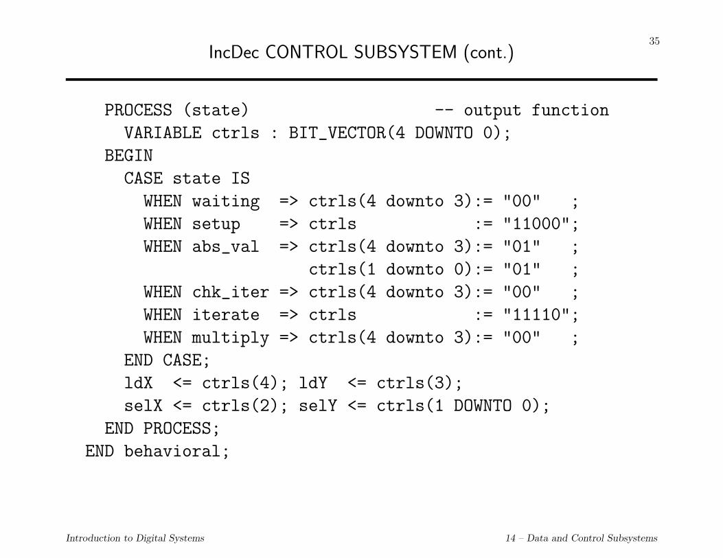
IncDec CONTROL SUBSYSTEM (cont.)
PROCESS (state) -- output function
VARIABLE ctrls : BIT_VECTOR(4 DOWNTO 0);
BEGIN
CASE state IS
WHEN waiting => ctrls(4 downto 3):= "00" ;
WHEN setup => ctrls := "11000";
WHEN abs_val => ctrls(4 downto 3):= "01" ;
ctrls(1 downto 0):= "01" ;
WHEN chk_iter => ctrls(4 downto 3):= "00" ;
WHEN iterate => ctrls := "11110";
WHEN multiply => ctrls(4 downto 3):= "00" ;
END CASE;
ldX <= ctrls(4); ldY <= ctrls(3);
selX <= ctrls(2); selY <= ctrls(1 DOWNTO 0);
END PROCESS;
END behavioral;
Introduction to Digital Systems 14 – Data and Control Subsystems

36
waiting
setup
abs_val
chk_iter
iterate
multiply
start
start’
k’
k
(a)
(b)
DMUX0 1
waiting
setup
abs_val
start
D
Qclk
clear
setD
Qclk
D
Qclk
D
Qclk
multiply
ldY
ldX
selX
selY
iterate
D
Qclk
chk_iter
DMUX0 1
k
D
Qclk
Figure 14.20: IMPLEMENTATION OF CONTROL SUBSYSTEM.
Introduction to Digital Systems 14 – Data and Control Subsystems

37
MICROPROGRAMMED CONTROLLER
• GENERALIZATION OF ROM-BASED CONTROLLER
• STATE-TRANSITION AND OUTPUT FUNCTIONS IMPLEMENTED US-ING TABLE LOOK-UP
• microinstruction – A WORD IN MEMORY SPECIFYING
1. THE VALUES OF THE CONTROL SIGNALS;
2. THE SEQUENCING INFORMATION THAT DETERMINES WHICH MI-CROINSTRUCTION IS EXECUTED NEXT
• microprogram - A SEQUENCE OF MICROINSTRUCTIONS
Introduction to Digital Systems 14 – Data and Control Subsystems

38
AddressGenerator
CSAR
ControlStore (CS)
Decoder
Mic
roco
ntro
ller
Externalcontrols
conditions(from datasubsystem)
Externaladdress
Branchaddress
Address mode
load
Operation mode
Control signals
Figure 14.21: A MICROPROGRAMMED CONTROLLER.
Introduction to Digital Systems 14 – Data and Control Subsystems

39
STRUCTURE (cont.)
• CONTROL STORE CS - CONTAINS THE MICROPROGRAM
– Uses ROM, PROM, or RAM
– ROM-based implementation is permanent; PROM or RAM-basedimplementations allow modifying the microprogram
– A RAM-based implementation: writable control store
– Systems with writable control store called microprogrammable
• CONTROL-STORE ADDRESS REGISTER (CSAR)
• CS ADDRESS GENERATOR (CSAGEN)
• DECODER - GENERATES CONTROL SIGNALS
• MICROCONTROLLER The “control unit” of the microprogrammedcontroller
Introduction to Digital Systems 14 – Data and Control Subsystems

40
ADVANTAGES AND DISADVANTAGES
+ The structure of the controller is modular, regular and independent of theparticular computation implemented by the system
+ The implementation of the controller for a complex computation consists ofwriting the corresponding microprogram
+ Simpler to write a microprogram than implement a fixed controller
+ Easily modified
- Might be slower
Introduction to Digital Systems 14 – Data and Control Subsystems

41
MICROINSTRUCTION FORMAT
• DIVIDED INTO FIELDS
• A CONTROL FIELD:contains the values of control signals
• A SEQUENCING FIELD:specifies the address of the next microinstruction
Introduction to Digital Systems 14 – Data and Control Subsystems

42
CONTROL FIELD
• HORIZONTAL (unpacked, decoded)
• VERTICAL (packed, encoded)
1 1 0 1
Horizontal format:
Control signals
4 2 3 3
16
Vertical format:
4 8 8
1101 01 101 001
Control signals
Decoders(optional)
(a) (b)
Figure 14.22: FORMATS OF THE CONTROL FIELD.
Introduction to Digital Systems 14 – Data and Control Subsystems

43
VERTICAL FORMAT (cont.)
– A DECODER PER SUBFIELD
– ALLOCATION TO SUBFIELDS
– ASSIGNED TO THE SAME SUBFIELD ONLY IF
• the operations they control are not required at the same time in themicroprogram; or
• the data subsystem does not allow the simultaneous use of such controlsignals.
Introduction to Digital Systems 14 – Data and Control Subsystems

44
EXAMPLE OF CONTROL FIELDS
(a)
R1clk
LDc_3
c_1 c_2
R7clk
LDc_21
c_19 c_20ALU OP
3
A_bus
B_bus
C_bus
(b)
Vertical format (12 bits):
A_bus B_busRegister
loads ALU
Horizontal format (24 bits):
Register transfer R_1 <= R_2 XOR R_6
(XOR code = 110)
Microinstructions: Horizontal format: c_3, c_4, c_17, c_22, c_23 = 1 other c_i = 0
Vertical format: 010 110 001 110(c)
c_1 c_24
Figure 14.23: VERTICAL AND HORIZONTAL ENCODING OF CONTROL FIELD for Example 14.1
Introduction to Digital Systems 14 – Data and Control Subsystems

45
MICROINSTRUCTION SEQUENCING
• EXPLICIT SEQUENCING
• IMPLICIT SEQUENCING
Explicit addressing scheme:
Implicit addressing scheme:
Branch address
Control signals1
0
Conditionfor branching
Control microinstruction
Branch microinstruction
Next microinstructionaddress
Control signals
(a)
(b)
Mode bit
Figure 14.24: MICROINSTRUCTION ADDRESSING SCHEMES: a) explicit sequencing; b) implicit sequencing.
Introduction to Digital Systems 14 – Data and Control Subsystems

46
IMPLICIT SEQUENCING
TWO TYPES OF CONTROL STORE ADDRESS CALCULATIONS REQUIRED:
• INCREMENT CSAR if not a branch, or if the condition not satisfied
• LOAD CSAR with the branch address if the current microinstruction is abranch and the condition satisfied.
Introduction to Digital Systems 14 – Data and Control Subsystems

47
MICROINSTRUCTION TIMING
1. LOADING THE ADDRESS of the next microinstruction into CSAR.
2. FETCHING (reading) the corresponding microinstruction
3. DECODING the fields.
4. EXECUTING the microoperations.
5. CALCULATING THE ADDRESS of the next microinstruction; this calculationcan be overlapped with the execution part of the cycle.
Fetch
Decode
Execute
Calculate address
Clock
Figure 14.25: MICROINSTRUCTION CYCLE.
Introduction to Digital Systems 14 – Data and Control Subsystems

48
EXAMPLE OF MICROPROGRAMMABLE SYSTEM
DATA SUBSYSTEM
• REGISTER FILE with 8 registers of 8 bits each. Two read and one writeoperations can be performed simultaneously.
• ALU: add, sub, xor and inc; conditions zero, neg and cy.
• 8-bit INPUT REGISTER.
• 8-bit OUTPUT REGISTER.
Introduction to Digital Systems 14 – Data and Control Subsystems

49
R_inclkLD
ALU
AB
Calu_op
2
cynegzeroRegister
File
fld_A3
3
3fld_B
fld_C
selR_in
R_outclkLD
clkldRF
ldR_in ldR_out
z_outx_in
alu_outMUX
8
8
8
8 8
88
8
01
Figure 14.26: DATA SUBSYSTEM.
Introduction to Digital Systems 14 – Data and Control Subsystems

50
EXAMPLE: CONTROL INPUTS TO DATA SUBSYSTEM
Control signal Descriptionfld A address for read port Afld B address for read port Bfld C address for writeldRF load register file (write)alu op operation performed in alu
00 - add
01 - sub
10 - xor
11 - inc
ldR in load R inldR out load R outselR in select R in
0 - select alu output1 - select R in
Introduction to Digital Systems 14 – Data and Control Subsystems

51
EXAMPLE: CONDITIONS
Condition Signal Descriptionalu out = 0 zero result is zeroalu out < 0 neg result is negativecarry cy result generated carry
Introduction to Digital Systems 14 – Data and Control Subsystems

52
BEHAVIORAL SPECIFICATION OF DATA SUBSYSTEM
ENTITY microdata IS
PORT(x_in : IN SIGNED(7 DOWNTO 0);
fld_A, fld_B, fld_C : IN UNSIGNED(2 DOWNTO 0);
alu_op : IN UNSIGNED(1 DOWNTO 0);
ldR_in, ldR_out, selR_in : IN STD_LOGIC ;
ldRF : IN STD_LOGIC ;
zero, neg, cy : OUT STD_LOGIC ;
z_out : OUT SIGNED(7 DOWNTO 0);
clk : IN STD_LOGIC);
END microdata;
ARCHITECTURE behavioral OF microdata IS
TYPE reg_fileT IS ARRAY(0 TO 7) OF SIGNED(7 DOWNTO 0);
SIGNAL RF: reg_fileT ;
SIGNAL R_in: SIGNED(7 DOWNTO 0);
BEGIN
PROCESS(clk)
VARIABLE A,B,C : SIGNED(7 DOWNTO 0);
VARIABLE alu_out: SIGNED(7 DOWNTO 0);
VARIABLE zzero,nneg,ccy: STD_LOGIC;
Introduction to Digital Systems 14 – Data and Control Subsystems

53
EXAMPLE: BEHAVIORAL DESCRIPTION (cont.)
BEGIN -- combinational modules
A:= RF(CONV_INTEGER(fld_A)); -- ALU
B:= RF(CONV_INTEGER(fld_B));
CASE alu_op IS
WHEN "00" => alu(zzero,nneg,ccy,alu_out,A,B,op_add);
WHEN "01" => alu(zzero,nneg,ccy,alu_out,A,B,op_sub);
WHEN "10" => alu(zzero,nneg,ccy,alu_out,A,B,op_xor);
WHEN "11" => alu(zzero,nneg,ccy,alu_out,A,B,op_inc);
WHEN OTHERS => NULL;
END CASE;
zero <= zzero; neg <= nneg; cy <= ccy;
IF (selR_in = ’0’) THEN C:= alu_out; -- multiplexer
ELSE C:= R_in ;
END IF;
IF (clk’EVENT AND clk = ’1’) THEN
IF (ldR_in = ’1’) THEN R_in <= x_in ; END IF;
IF (ldR_out = ’1’) THEN z_out<= alu_out; END IF;
IF (ldRF = ’1’) THEN RF(CONV_INTEGER(fld_C))<= C; END IF;
END IF;
END PROCESS;
END behavioral;
Introduction to Digital Systems 14 – Data and Control Subsystems

54
CONTROL SUBSYSTEM - MICROPROGRAMMED
Inputs: start
zero, neg, cy
Outputs: fld A, fld B, fld C
alu op
ldR in, ldR out
selR in, ldRF, done
• IMPLICIT SEQUENCING
• TWO MICROINSTRUCTION FORMATS: operations and branch
Control format:
Branch format:
fld_A fld_B fld_Calu_ops_d
0
r_d
1
cond
ition
branch addresscond
_val
ldRF
ldR_out
ldR_in
selR_in
Figure 14.28: MICROINSTRUCTION FORMATS.
Introduction to Digital Systems 14 – Data and Control Subsystems

55
ENCODING OF FIELDS
• Field cond encoding
Condition Codestart 00zero 01neg 10cy 11
• Field cond val specifies the value of the conditionfor the branch to execute
Introduction to Digital Systems 14 – Data and Control Subsystems

56
BEHAVIORAL DESCRIPTION OF CONTROL SUBSYSTEM
ENTITY microctrl IS
GENERIC(cssize: NATURAL:=16);
PORT(start,zero,neg,cy: IN STD_LOGIC ;
fld_A,fld_B,fld_C: OUT UNSIGNED(2 DOWNTO 0);
alu_op : OUT UNSIGNED(1 DOWNTO 0);
ldR_in,ldR_out : OUT STD_LOGIC ;
selR_in,ldRF,done: OUT STD_LOGIC ;
clk : IN STD_LOGIC );
END microctrl;
ARCHITECTURE behav_microprogr OF microctrl IS
SIGNAL csar : NATURAL ; -- state
SIGNAL uinstr : UNSIGNED(17 DOWNTO 0); -- microinstruction
ALIAS mode : STD_LOGIC IS uinstr(17); -- branch mode
ALIAS condition: UNSIGNED(1 DOWNTO 0) IS uinstr(16 DOWNTO 15);
ALIAS cond_val : STD_LOGIC IS uinstr(14); -- condition value
PROCESS(clk)
VARIABLE index: UNSIGNED(13 DOWNTO 0);
Introduction to Digital Systems 14 – Data and Control Subsystems

57
BEHAVIORAL DESCRIPTION OF CONTROL SUBSYSTEM: TransitionFunction
BEGIN
IF (clk’EVENT AND clk = ’1’) THEN
IF (mode = ’0’) THEN csar <= csar + 1;
ELSE
CASE condition IS
WHEN "00" => IF (start = cond_val) THEN
index:= uinstr(13 DOWNTO 0);
csar <= CONV_INTEGER(index);
ELSE csar <= csar + 1;
END IF;
WHEN "01" => IF (zero = cond_val) THEN
index:= uinstr(13 DOWNTO 0);
csar <= CONV_INTEGER(index);
ELSE csar <= csar + 1;
END IF;
Introduction to Digital Systems 14 – Data and Control Subsystems

58
TRANSITION FUNCTION (cont.)
WHEN "10" => IF (neg = cond_val) THEN
index:= uinstr(13 DOWNTO 0);
csar <= CONV_INTEGER(index);
ELSE csar <= csar + 1;
END IF;
WHEN "11" => IF (cy = cond_val) THEN
index:= uinstr(13 DOWNTO 0);
csar <= CONV_INTEGER(index);
ELSE csar <= csar + 1;
END IF;
WHEN OTHERS => NULL;
END CASE;
END IF;
END IF;
END PROCESS;
Introduction to Digital Systems 14 – Data and Control Subsystems

59
BEHAVIORAL DESCRIPTION: OUTPUT FUNCTION
PROCESS (csar) -- output function
TYPE csarray IS ARRAY(0 to cssize-1)
OF UNSIGNED(17 DOWNTO 0);
VARIABLE cs: csarray
-- here the microprogram as initial contents of ARRAY cs
:= (0 => "001000000000100010",
1 => "100000000000000001",
2 => "011000000011110001",
3 => "000000000010100100",
4 => "000000000111100000",
5 => "000010010010100000",
6 => "111000000000001000",
7 => "011111000111100000",
8 => "000011011011100000",
9 => "111000000000000101",
10 => "000111000111101000",
11 => "111000000000000000");
-- Continuation --
Introduction to Digital Systems 14 – Data and Control Subsystems

60
BEHAVIORAL DESCRIPTION: Check Mode
BEGIN
uinstr <= cs(csar);
CASE uinstr(17) IS -- check mode
WHEN ’0’ => alu_op <= uinstr(16 DOWNTO 15);
fld_A <= uinstr(14 DOWNTO 12);
fld_B <= uinstr(11 DOWNTO 9);
fld_C <= uinstr( 8 DOWNTO 6);
ldRF <= uinstr(5);
ldR_in <= uinstr(4);
ldR_out<= uinstr(3);
selR_in<= uinstr(2);
IF (uinstr(1) = ’1’) THEN done <= ’1’; END IF;
IF (uinstr(0) = ’1’) THEN done <= ’0’; END IF;
WHEN ’1’ => ldRF <= ’0’; ldR_out <= ’0’; ldR_in <= ’0’;
WHEN OTHERS => NULL;
END CASE; END PROCESS; END behav_microprogr;
Introduction to Digital Systems 14 – Data and Control Subsystems

61
STRUCTURAL DESCRIPTION
Datasubsystem
x_in
clk
fldA
fldB
fldC
alu_op
ldR_in
ldR_out
selR_inz_out
zero
neg
cy
start
done
Controlsubsystem
ldRF
Figure 14.31: BLOCK DIAGRAM
Introduction to Digital Systems 14 – Data and Control Subsystems

62
STRUCTURAL DESCRIPTION (cont.)
ARCHITECTURE structural OF micro IS
SIGNAL fld_A,fld_B,fld_C: UNSIGNED(2 DOWNTO 0);
SIGNAL alu_op : UNSIGNED(1 DOWNTO 0);
SIGNAL zero, neg, cy : STD_LOGIC ;
SIGNAL ldR_in,ldR_out : STD_LOGIC ;
SIGNAL selR_in,ldRF : STD_LOGIC ;
BEGIN
U1: ENTITY microdata
PORT MAP(x_in,fld_A,fld_B,fld_C,alu_op,
ldR_in,ldR_out,selR_in,ldRF,zero,neg,cy,z_out,clk);
U2: ENTITY microctrl
PORT MAP(start,zero,neg,cy,fld_A,fld_B,fld_C,alu_op,
ldR_in,ldR_out,selR_in,ldRF,done,clk);
END structural;
Introduction to Digital Systems 14 – Data and Control Subsystems

63
Example 14.3: COUNTING THE NUMBER OF ONES
• Count the number of 1’s in an 8-bit input vector
• Use the system of Fig. 14.26
R_inclkLD
ALU
AB
Calu_op
2
cynegzeroRegister
File
fld_A3
3
3fld_B
fld_C
selR_in
R_outclkLD
clkldRF
ldR_in ldR_out
z_outx_in
alu_outMUX
8
8
8
8 8
88
8
01
Figure 14.26: DATA SUBSYSTEM.
Introduction to Digital Systems 14 – Data and Control Subsystems

64
SPECIFICATION OF SYSTEM IN Example 14.3
ENTITY micro IS
PORT(start: IN STD_LOGIC ; -- start signal
x_in : IN SIGNED(7 DOWNTO 0); -- input vector
z_out: OUT SIGNED(7 DOWNTO 0); -- result
done : OUT STD_LOGIC ; -- done signal
clk : IN STD_LOGIC) ;
END micro;
ARCHITECTURE specif OF micro IS
BEGIN
PROCESS (start)
VARIABLE x,n: SIGNED(7 DOWNTO 0);
BEGIN
IF (start’EVENT AND start = ’1’) THEN
done <= ’0’;
x:= x_in; n:= (OTHERS => ’0’);
FOR i IN 1 TO 8 LOOP
IF (x(x’LEFT) = ’1’) THEN n:= n+1; END IF;
x:= x(x’LEFT-1 DOWNTO 0) & ’0’ ;
END LOOP;
z_out <= n;
done <= ’1’;
END IF;
END PROCESS;
END specif;
Introduction to Digital Systems 14 – Data and Control Subsystems

65
mode alu op fld ldRF ldR selR s d r d control
A B C in out in format
mode (cond., branch address branch
cond val) format
0: 0 sub=01 0 0 0 1 0 0 0 1 0 R0 <- 0;
set done
1: 1 (start,0) 1 branch if
=000 start = 0
2: 0 inc=11 0 0 3 1 1 0 0 0 1 input x in;
R3 <- 1;
clear done
3: 0 add=00 0 0 2 1 0 0 1 0 0 R2 <- Rin;
4: 0 add=00 0 0 7 1 0 0 0 0 0 R7 <- 0;
5: 0 add=00 2 2 2 1 0 0 0 0 0 R2 <- R2+R2;
6: 1 (cy,0) 8 branch if
=110 cy = 0
7: 0 inc=11 7 0 7 1 0 0 0 0 0 R7 <- R7+1;
8: 0 add=00 3 3 3 1 0 0 0 0 0 R3 <- R3+R3
9: 1 (cy,0) 5 branch if
=110 cy = 0
10: 0 add=00 7 0 7 1 0 1 0 0 0 Rout <- R7;
11: 1 (cy,0) 0 done;
=110 branch to 0
Figure 14.33: MICROPROGRAM FOR Example 14.3.Introduction to Digital Systems 14 – Data and Control Subsystems
66
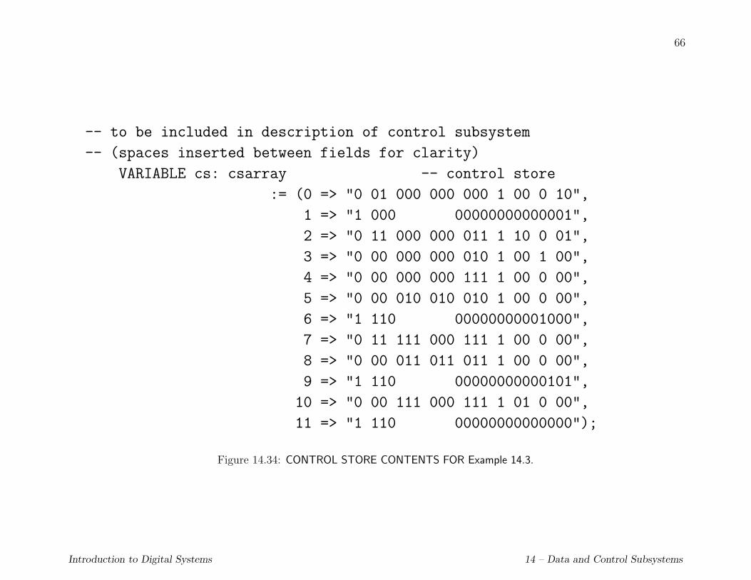
-- to be included in description of control subsystem
-- (spaces inserted between fields for clarity)
VARIABLE cs: csarray -- control store
:= (0 => "0 01 000 000 000 1 00 0 10",
1 => "1 000 00000000000001",
2 => "0 11 000 000 011 1 10 0 01",
3 => "0 00 000 000 010 1 00 1 00",
4 => "0 00 000 000 111 1 00 0 00",
5 => "0 00 010 010 010 1 00 0 00",
6 => "1 110 00000000001000",
7 => "0 11 111 000 111 1 00 0 00",
8 => "0 00 011 011 011 1 00 0 00",
9 => "1 110 00000000000101",
10 => "0 00 111 000 111 1 01 0 00",
11 => "1 110 00000000000000");
Figure 14.34: CONTROL STORE CONTENTS FOR Example 14.3.
Introduction to Digital Systems 14 – Data and Control Subsystems


![An Approximation Algorithm for Scheduling on …web.cs.ucla.edu/~ani/publications/[TECS2009]ApproxAlg_a5... · 5 An Approximation Algorithm for Scheduling on Heterogeneous Reconfigurable](https://static.fdocuments.in/doc/165x107/5aea34cf7f8b9ac3618d789b/an-approximation-algorithm-for-scheduling-on-webcsuclaeduanipublicationstecs2009approxalga55.jpg)